EP0012840B1 - Line-addressable memory with serial-parallel-serial configuration - Google Patents
Line-addressable memory with serial-parallel-serial configuration Download PDFInfo
- Publication number
- EP0012840B1 EP0012840B1 EP79104586A EP79104586A EP0012840B1 EP 0012840 B1 EP0012840 B1 EP 0012840B1 EP 79104586 A EP79104586 A EP 79104586A EP 79104586 A EP79104586 A EP 79104586A EP 0012840 B1 EP0012840 B1 EP 0012840B1
- Authority
- EP
- European Patent Office
- Prior art keywords
- line
- serial
- parallel
- phase
- electrode
- Prior art date
- Legal status (The legal status is an assumption and is not a legal conclusion. Google has not performed a legal analysis and makes no representation as to the accuracy of the status listed.)
- Expired
Links
Images


Classifications
-
- G—PHYSICS
- G11—INFORMATION STORAGE
- G11C—STATIC STORES
- G11C19/00—Digital stores in which the information is moved stepwise, e.g. shift registers
- G11C19/28—Digital stores in which the information is moved stepwise, e.g. shift registers using semiconductor elements
- G11C19/287—Organisation of a multiplicity of shift registers
-
- H—ELECTRICITY
- H01—ELECTRIC ELEMENTS
- H01L—SEMICONDUCTOR DEVICES NOT COVERED BY CLASS H10
- H01L27/00—Devices consisting of a plurality of semiconductor or other solid-state components formed in or on a common substrate
- H01L27/02—Devices consisting of a plurality of semiconductor or other solid-state components formed in or on a common substrate including semiconductor components specially adapted for rectifying, oscillating, amplifying or switching and having at least one potential-jump barrier or surface barrier; including integrated passive circuit elements with at least one potential-jump barrier or surface barrier
- H01L27/04—Devices consisting of a plurality of semiconductor or other solid-state components formed in or on a common substrate including semiconductor components specially adapted for rectifying, oscillating, amplifying or switching and having at least one potential-jump barrier or surface barrier; including integrated passive circuit elements with at least one potential-jump barrier or surface barrier the substrate being a semiconductor body
- H01L27/10—Devices consisting of a plurality of semiconductor or other solid-state components formed in or on a common substrate including semiconductor components specially adapted for rectifying, oscillating, amplifying or switching and having at least one potential-jump barrier or surface barrier; including integrated passive circuit elements with at least one potential-jump barrier or surface barrier the substrate being a semiconductor body including a plurality of individual components in a repetitive configuration
- H01L27/105—Devices consisting of a plurality of semiconductor or other solid-state components formed in or on a common substrate including semiconductor components specially adapted for rectifying, oscillating, amplifying or switching and having at least one potential-jump barrier or surface barrier; including integrated passive circuit elements with at least one potential-jump barrier or surface barrier the substrate being a semiconductor body including a plurality of individual components in a repetitive configuration including field-effect components
- H01L27/1057—Devices consisting of a plurality of semiconductor or other solid-state components formed in or on a common substrate including semiconductor components specially adapted for rectifying, oscillating, amplifying or switching and having at least one potential-jump barrier or surface barrier; including integrated passive circuit elements with at least one potential-jump barrier or surface barrier the substrate being a semiconductor body including a plurality of individual components in a repetitive configuration including field-effect components comprising charge coupled devices [CCD] or charge injection devices [CID]
Definitions
- the present invention relates to a line-addressable memory with serial bit input and output according to the preamble of claim 1.
- charge coupling elements in data memories, primarily in the form of shift registers, into which data are read out again as a serial bit stream at one end of the shift register and the other end, is generally known in the art.
- serial-parallel-serial shift register according to US-A-3 967 254 made of charge coupling elements.
- Such a memory consists of three main parts. The first part is used for bit-by-bit data entry into a serial input register. In the second part, data is transferred in parallel from the serial input register to a parallel part. This is commonly referred to as a row of data in the parallel part.
- the parallel part typically contains many lines because most of the data is stored here. While individual data bits were initially entered bit by bit into the serial input register, the forwarding through the parallel register is now done line by line.
- the individual bits continue to run in their respective channels, commonly called columns. These columns are orthogonal to the rows.
- data is transferred from the last line of the parallel part to the serial output register, from where it is read out bit by bit. The output can then be transmitted to a user device and / or returned to the input of the serial input register for further data storage.
- serial-parallel-serial circuit has a number of advantages, but of course also inherent disadvantages.
- the advantages include the storage density, the low storage costs per bit and the lower power consumption.
- a major disadvantage, however, is the high latency, because the bits can only be read in the exact order in which they were originally written. So if the user device needs data that has just been written into the serial input register, the entire memory must first circulate before this information is available at the serial output register. In order to be able to address the data better at random, conventional memories with row addressing were developed. In such a memory according to US Pat. No. 4,024,512, data is entered into a row of shift registers and read out from there.
- the object of the invention is to provide an improved electronic data storage device which has both the properties of a serial-parallel-serial data storage device and that of a line-addressable data storage device which is composed of charge coupling elements and from which the data are read out serially in more than one operating mode can.
- a circuit according to the invention can be operated fully as a standard PLC circuit configuration.
- data bits are entered serially into the serial input register 10 from left to right.
- the desired number of bits have been entered into the input register 10, they are input in parallel via the series / parallel converter 16 into a first line of the parallel central part 12.
- new data are entered into the serial input register 10 and again entered into the first line of the parallel central part 12 by the series / parallel converter 16, while the data previously there are placed in the second line.
- the parallel central part 12 is filled with data line by line.
- the parallel / series converter 18 When the data entered first reaches the last line of the parallel central part 12, it is passed in parallel through the parallel / series converter 18 into the serial output register 14.
- data is passed bit by bit into the query amplifier 22 and from there to the data output connection and to the specified input of the control and clock switching block 20.
- circulation mode the data at the data output connection are not used, but the bits coming from the query amplifier 22 are re-entered into the serial input register 10 via the control and clock switch block 20. This continuous circulation of the data bit stream prevents loss of information in the charge coupling elements.
- a data record must be able to be entered and output as shown by hatching in FIG. 1.
- the bit positions have been designated in Fig. 1.
- the arrangement contains N-1 lines in the parallel central part, of which the first line stores the Z bits, while the N-1 line stores the B bits. (M + 1) x N bits are stored in total because the A bits are stored in the serial output register.
- Each column stores a desired data set, which consists of data bits A to Z.
- the hatched cells show the serial path on which a data record is entered or output.
- data set 2 i.e. H. A2 B2 ... Z2
- the data record is analogous to the row-addressable column of a conventional row-addressable structure.
- the input register 10 was filled with zero bits.
- the hatched bits can be read out in the following order: A0, A1, A2, B2 to Z2 and the zero bits, as shown in the hatched part of the register. While these bits are being read out at the data output connection, they also circulate through the control and clock switching block 20, so that at the end of the operation exactly the configuration shown in FIG. 1 is restored. Now you can either use a different data set, e.g. B. A3 to Z3, address or resume the renewal with a conventional PLC operation. Of course, while a desired line is being addressed, all other bits in the parallel channels remain inactive, i.e. they will not be forwarded.
- FIG. 2A to 2F the example shown in detail uses the embodiment shown in FIG. 1, in which the empty or zero bits are in the input register 10.
- the series / parallel converter 16 and the parallel / series converter 18 from FIG. 1 have been deliberately omitted for the sake of simplicity.
- the designation of the bits has been changed slightly for the same reason.
- data record No. 2 consisting of bits A, B, C, D to Z
- a counter at the output connection in the user device shows that bits WO and W1 correspond to the first two data records and are therefore not part of the addressed line.
- the bit WO is the first outgoing bit that is also written into the first bit position in the serial input register 10 when each bit is shifted by one position.
- 2C shows the situation when each bit has been shifted by a further position, with W1 being read out and placed in the first bit position in the serial register 10, while all other bits are shifted accordingly by one position.
- 2D shows how the reading of the addressed line begins with the reading out of bit A.
- a new bit A with the designation A ' is applied to the input connection and set in the first bit position of the input register 10. All bits are shifted accordingly as previously described.
- the latency in the worst case is the shift time of M bits if any data set is desired. In the case shown in FIG. 1, the latency is only as long as the shift time for bits AO and A1. However, another move must be made to restore the data to its original configuration and complete the operation.
- FIG. 3 An exemplary structure for performing this function is shown in FIG. 3, where P + regions 31, 32, 33, 34, 35, 36 and 37 were created in a P-type substrate by ion implantation. Details of each cell are shown on cell 1, 2 and 3. Each cell has three electrodes, namely a DC control line, a phase 1 (P1) and a phase 2 (P2). By applying three different potential levels to the three different electrodes, it is known that three different energy levels can be created in each cell. The additional ion implantation under part of the gate electrode, however, allows two energy levels to be created under this gate electrode. By ion implantation 31 under part of the gate electrode for phase 1, two separate energy levels can thus be created under this gate electrode. The same applies to ion implantation 32 under the gate electrode of phase 2.
- FIG. 3E shows the applied potential levels
- FIGS. 3A to 3D illustrate the transfer of charge through the cells.
- the figures 3A to 3E show the state in which charge is passed through the circuit arrangement. This process takes place in every line during the PLC operation.
- the figures 3A to 3E show the state of the addressed line in the line addressing mode.
- the potential levels applied at time t oo are shown in FIG. 3E.
- the DC voltage control line and the line for phase 1 are at a low level, the line for phase 2 is at a high level. This results in the potential well configuration shown in Fig. 3A.
- a binary 1 is stored in cell 1 and in the previous cell, while zeros are stored in cells 2 and 3.
- the DC control line is brought to a high level, while the signal level on the lines for phases 1 and 2 is not changed.
- the potential wells are arranged differently, as shown in FIG. 3B.
- the electrode for phase 1 was brought to a high signal level, while the electrode for phase 2 was brought to a low level and the control line was kept at a high level.
- the DC control line is held at a high level, while the line for phase 1 has been brought low and the line for phase 1 has been brought high. This leads to the distribution of the potential wells shown in FIG. 3D.
- the La Broadcasting is essentially complete, with cell 1 containing a binary 1 that was previously in the previous cell, cell 2 is also a binary 1 that was previously in cell 1, and cell 3 contains the fat zero that was previously in cell 2 stood.
- FIG. 4 shows the same structure as FIG. 3.
- the initial states of the control lines in FIG. 4E are identical to those of FIG. 3E at time t oo .
- identical binary data are stored as shown in FIG. 4A, as in FIG. 3A.
- FIG. 4A is identical to FIG. 3A.
- the potential wells in FIG. 4B are absolutely identical to those in FIG. 4A.
- a circuit is described in connection with FIG. 5 which is suitable for executing the PLC operation and the line addressing operation.
- Commonly known operations such as transfers within a serial register, transfers within a parallel register and serial / parallel conversions or parallel / serial conversions, as well as other details of charge generation and sensing are not described in detail since they are generally known.
- FIG. 5 One aspect of the configuration shown in FIG. 5 is the use of DC controlled charge coupling elements for the line addressable PLC memory array.
- charge coupling elements require a DC control line for each parallel channel, but can be operated with common clock lines for all parallel channels. This is an important point in that it enables a very dense circuit arrangement. This means that all circuit and space savings can be directly attributed to the concept of the row-addressable serial-parallel-serial memory arrangement.
- Fig. 5 shows primarily the running of the clock and control lines.
- the serial input register 10, the parallel middle part 12 and the serial output register 14 are again numbered in the same way as in the previous drawings.
- the serial input register 10 receives an input in a generation part and it receives the connection of the electrodes for phases 1 and phase 2.
- the blocking lines (S1) from the channel selector are present here. These are the DC control lines described above that must be selectively activated during row addressing.
- data bits are selectively transmitted in all serial input registers and in line addressing mode, depending on the addressed line, as was described, for example, in connection with FIG. 1.
- the two cell groups of the serial input register 10 are arranged exactly as described above in connection with FIGS. 3 and 4 has been described.
- the parallel part the one selected and all other cell divisions are arranged exactly as described above in connection with FIGS. 3 and 4 has been described.
- the connection of the parallel channel clock lines for phases 1 and 2 is particularly shown.
- the temporal relationship of phase 1 to phase 2 in the serial and parallel part is selected as desired and depending on the type in which the series / parallel conversion is to take place (see FIGS. 3E and 4E).
- serial channel control lines are controlled by the channel decoder / selector which receives a channel address.
- the channel decoder / selector also controls the serial channel control lines (S3) in the serial output register 14. After the bits have been transferred from the last line of the parallel central part 12 (either in parallel in the PLC mode or bit by bit as in the line address mode), they become serial from the serial output register 14 by the clock pulses of phase 1 and phase 2 via the detector to the output port.
- FIG. 6 is an enlarged illustration of the structure shown in FIG. 5 in the area of the section line 6.
- the substrate 60 is typically doped with P-type impurities.
- the production of charge coupling elements with N-type substrates is of course also known. Ion implantations and the various electrodes made of polysilicon and metal are produced in the arrangement shown using known lithography technology.
- the clock lines for phase 1 are formed with the polysilicon electrodes 62 and 64, the electrode 62 being designated poly 1 and the electrode 64 being designated poly 2. This designation was established in the order in which the various polysilicon electrodes with the various insulating layers between them are formed from silicon dioxide.
- the phase 2 clock lines are formed by the polysilicon electrodes 62 'and 64'.
- the uppermost layer conductor (generally made of metal) is the blocking line 66 for one column and the blocking line 66 'for the other column.
- the first column is separated from the second column by a recessed oxide insulation 67 '.
- the first column is separated from the other adjacent column by the oxide recess 67, while the second column shown is separated from the next adjacent column by the recessed oxide 67 ".
- Oxide isolation as well as other types of insulation between the columns are well known for the present invention However, it is particularly useful when the overall structure corresponds to the known PLC arrangement in all possible respects, but differs from it by the additional line addressing device described here.
- FIG. 6A shows a vertical section through the structure of FIG. 6 along the section line 6A.
- Fig. 6A is a detailed illustration of that associated with Figs. 3 and 4 described schemes.
- the various electrodes 62, 64 and 66 as well as the ion implantations 68, 68 'etc. are formed on the substrate 60. With a P-type substrate, the ion implantations are P + -conductive.
- the barrier electrode is generally a metal, but triple polystructures are also known. Electrode 66 may as well be made of polysilicon.
- the various electrodes and the substrate are suitably insulated from one another by silicon dioxide.
- FIGS. 3 and 4 A typical cell, e.g. cell 1 in FIGS. 3 and 4 is shown in Fig. 6A.
- the electrode for phase 1 (P1) contains poly 1 (62) and poly 2 (64) and clearly shows the one in FIGS. 3 and 4 only schematically shown connection of the two electrodes.
- the ion implantation 68 was formed under the poly 2 electrode 64.
- phase 2 is connected to the electrode 62 '(poly 1) and 64' (poly 2), the latter being formed above the ion implantation 68 '.
- the last connection for this cell is the DC control electrode 66 (blocking electrode).
- the thin oxide layer 69 need not be equal, for example the first thickness t below the polysilicon electrodes 62 and 64 may be of the order of 5 ⁇ 10 -8 m (500 ⁇ ).
- a second thickness t 2 below the metallic control electrodes (feed electrodes) can be in the order of 10-7 m (1000 ⁇ ).
- FIG. 7 is an enlargement of the representation in FIG. 5 in the area of the section lines 7A and 7B.
- the substrate was designated with the reference number 70. The region shown enlarged in FIG.
- FIG. 7 contains part of the parallel channel, part of the parallel / series converter and part of the serial channel.
- section line 7B part of the parallel channel, part of the parallel / series converter and part of the serial channel are shown in FIG. 7.
- only part of the serial channel is shown in FIG. 7 along the section line 7A.
- the clock lines for phase 2 are formed by electrodes 82 and 84, electrode 82 being poly 1 and electrode 84 being poly 2.
- the electrodes 82 'and 84' for the clock phase 1 formed by poly 1 and poly 2.
- the electrodes 72 and 74 for the clock phase 2 are formed by poly 1 and poly 2.
- the parallel channel control lines 76 (blocking lines) run from the parallel channel via the serial channel, but do not influence this, because they are separated from the substrate by a thick oxide layer.
- the serial control electrodes 77 are only in the serial channel area and have the same blocking or transfer function as described above for the parallel channel control lines.
- FIG. 7A shows a vertical section through the structure shown in FIG. 7 along the section line 7A.
- a part of the serial output register is shown (the serial input register has cells of the same structure, of course).
- a plurality of P + -conducting ion implantations 71, 71 ', 71 ", 71'" are formed in the P-type substrate.
- the poly 1 electrode 72 and the poly 2 electrode 74 are suitably insulated from one another by silicon dioxide.
- the parallel channel control lines 76 are not separated from the substrate by a thick oxide, but also by the corresponding polysilicon electrodes, and therefore have no influence on the forwarding of the Charge. However, the serial conductors 77 are separated from the substrate only by a thin oxide.
- the metal control electrode separated from the substrate thick oxide may be about 10 ⁇ 7 to be m (1000 ⁇ ) thick, that the poly electrodes from the substrate separating thin oxide about 5 ⁇ 10 -8 m (500A).
- the typical cell shown in FIG. 7A has the serial control electrodes 77 as the control electrode.
- the line for the clock phase 2 is connected to both the poly 1 electrode 72 and the poly 2 electrode 74, which lies essentially above the ion implantation 71.
- the control line for phase 1 is connected to poly 1 Electrode 72 and the poly 2 electrode 74 connected, which lies essentially over the ion implantation 71 '. In this circuit arrangement, the charge is passed from right to left.
- FIG. 7B shows a section through the structure shown in FIG. 7 along the section line 7B.
- the electrodes for the clock phase 2 are formed by the poly 1 electrode 82 and the poly 2 electrode 84, which lies essentially above the ion implantation 88.
- the electrodes for clock phase 1 are formed by the partially shown poly 1 electrode 82 with another poly 2 electrode (not shown).
- the control electrode 76 forms the blocking contact for the cell shown in the parallel channel part.
- the electrodes for the clock phase 1 are formed by the poly 1 electrode 82 'and the poly 2 electrode 84', which lies essentially above the ion implantation 88 '.
- the serial channel portion is better shown in Figure 7A.
- a typical recessed oxide insulation 90 is shown to the right of the serial channel portion in FIG. 7B.
- the substrate was numbered 80 in Figure 7B.
- a two-phase embodiment of the invention has been described above. Common clock lines are used for each memory column, as is common in PLC circuitry. This maintains the high density of the PLC circuits. For the increased flexibility of row addressing, only one DC control line is required for each channel.
- the use of a third level conductor for the DC control electrodes (blocking electrodes) is not a significant burden for an existing PLC circuit. Since a metal plane is usually an integrated part in the manufacture of a charge coupling element with two self-aligning polysilicon electrodes, the use of metal for the DC control electrodes is very convenient.
- the use of metal electrodes on thin oxide is more reliable if the thin oxide is thicker under the metal than under the polysilicon, because the DC control electrodes need to change the energy level between them only about half as much as the electrodes under the polysilicon. Due to a thicker oxide layer under the metal electrodes, the same DC voltage applied under these metal electrodes causes less energy change. On the other hand, smaller DC voltages can be applied to the metal electrodes, so that the thin oxide can have a uniform thickness everywhere.
- the relative voltage levels for clock phases 1 and 2 and the DC voltage control electrodes are known per se, with which the potential barriers shown are erected under the various control electrodes.
- the low level for the two clock signals phase 1 and phase 2 must have a sufficiently high voltage so that the directional barrier under the ion implantation does not exceed that under the DC control electrodes.
- the sense of direction in two-phase charge coupling elements can also be achieved using techniques other than ion implantation, for example by displacing thin and thick oxide.
- a line-addressable circuit arrangement can also be modified in such a way that it contains a PLC function.
Landscapes
- Engineering & Computer Science (AREA)
- Power Engineering (AREA)
- Physics & Mathematics (AREA)
- Condensed Matter Physics & Semiconductors (AREA)
- General Physics & Mathematics (AREA)
- Computer Hardware Design (AREA)
- Microelectronics & Electronic Packaging (AREA)
- Dram (AREA)
- Solid State Image Pick-Up Elements (AREA)
Description
Die vorliegende Erfindung betrifft einen zeilenadressierbaren Speicher mit serieller Biteingabe und -ausgabe nach dem Oberbegriff des Anspruchs 1.The present invention relates to a line-addressable memory with serial bit input and output according to the preamble of
In der Technik ist die Verwendung von Ladungskopplungselementen in Datenspeichern, primär in der Form von Schieberegistern, in die Daten als serieller Bitstrom an einem Ende des Schieberegisters ein- und anderen Ende wieder ausgelesen werden, allgemein bekannt.The use of charge coupling elements in data memories, primarily in the form of shift registers, into which data are read out again as a serial bit stream at one end of the shift register and the other end, is generally known in the art.
Ein wesentlicher Fortschritt war das seriell-parallel-seriell geschaltete Schieberegister gemäss US-A-3 967 254 aus Ladungskopplungselementen. Ein solcher Speicher besteht aus drei Hauptteilen. Der erste Teil dient der bitweisen Dateneingabe in ein serielles Eingaberegister. Im zweiten Teil werden Daten parallel vom seriellen Eingaberegister in einen parallelen Teil übertragen. Das wird allgemein als eine Datenzeile im parallelen Teil bezeichnet. Der parallele Teil enthält typischerweise viele Zeilen, weil hier der grösste Teil der Daten gespeichert wird. Während einzelne Datenbits am Anfang bitweise in das serielle Eingaberegister eingegeben wurden, erfolgt die Weiterleitung durch das parallele Register jetzt zeilenweise.A major advance was the serial-parallel-serial shift register according to US-A-3 967 254 made of charge coupling elements. Such a memory consists of three main parts. The first part is used for bit-by-bit data entry into a serial input register. In the second part, data is transferred in parallel from the serial input register to a parallel part. This is commonly referred to as a row of data in the parallel part. The parallel part typically contains many lines because most of the data is stored here. While individual data bits were initially entered bit by bit into the serial input register, the forwarding through the parallel register is now done line by line.
Tatsächlich laufen die einzelnen Bits in ihren betreffenden Kanälen, die üblicherweise Spalten genannt werden, weiter. Diese Spalten verlaufen othogonal zu den Zeilen. Im dritten Teil werden Daten aus der letzten Zeile des parallelen Teiles in das serielle Ausgaberegister übertragen, von wo sie seriell bitweise ausgelesen werden. Die Ausgabe kann dann an ein Benutzergerät übertragen und/oder an den Eingang des seriellen Eingaberegisters zur weiteren Datenspeicherung zurückgeleitet werden.In fact, the individual bits continue to run in their respective channels, commonly called columns. These columns are orthogonal to the rows. In the third part, data is transferred from the last line of the parallel part to the serial output register, from where it is read out bit by bit. The output can then be transmitted to a user device and / or returned to the input of the serial input register for further data storage.
Die oben allgemein beschriebene Anordnung, in breitem Rahmen serielle-parallele-serielle Schaltung genannt, hat eine Anzahl von Vorteilen, aber natürlich auch inhärente Nachteile. Zu den Vorteilen gehören die Speicherdichte, die niedrigen Speicherkosten pro Bit und der geringere Stromverbrauch. Ein Hauptnachteil besteht jedoch in der grossen Latenzzeit, weil die Bits immer nur in genau derselben Reihenfolge ausgelesen werden können, in der sie ursprünglich eingeschrieben wurden. Wenn das Benutzergerät also Daten braucht, die gerade in das serielle Eingaberegister eingeschrieben wurden, muss der ganze Speicher erst umlaufen, bevor diese Information am seriellen Ausgaberegister zur Verfügung steht. Um die Daten besser wahlfrei adressieren zu können, wurden herkömmliche Speicher mit Zeilenadressierung entwickelt. Bei einem solchen Speicher gemäss US-PS 40 24 512 werden Daten in eine Zeile von Schieberegistern eingegeben und von dort ausgelesen. Zur Beschreibung sei angenommen, dass diese Zeilen in derselben Richtung laufen wie die vorher in der SPS-Struktur definierten Spalten. Eine mögliche praktische Ausführung besteht darin, dass jede zweite Spalte in der entgegengesetzten Richtung weiterleitet, was zu kontinuierlichen Schleifen führt, die von jedem Spaltenpaar gebildet werden. Der zeilenadressierbare Speicher enthält viele derartige Schleifen, die parallel arbeiten. Wie der Name schon sagt, hat der zeilenadressierbare Speicher eine ausreichende Beweglichkeit zum Auslesen aus irgendeiner Spalte oder Schleife. Das Benutzergerät hat also direkten Zugriff zu den gewünschten Daten (Latenzzeit Null). Diese stark verbesserte Arbeitsgeschwindigkeit gegenüber einer seriellen-parallelen-seriellen Struktur geht jedoch auf Kosten einer geringeren Bitdichte und eines grösseren Stromverbrauches, die beide zu höheren Speicherkosten pro Bit führen.The arrangement generally described above, broadly called serial-parallel-serial circuit, has a number of advantages, but of course also inherent disadvantages. The advantages include the storage density, the low storage costs per bit and the lower power consumption. A major disadvantage, however, is the high latency, because the bits can only be read in the exact order in which they were originally written. So if the user device needs data that has just been written into the serial input register, the entire memory must first circulate before this information is available at the serial output register. In order to be able to address the data better at random, conventional memories with row addressing were developed. In such a memory according to US Pat. No. 4,024,512, data is entered into a row of shift registers and read out from there. For the description it is assumed that these lines run in the same direction as the columns previously defined in the PLC structure. One possible practical implementation is that every second column forwards in the opposite direction, which leads to continuous loops formed by each pair of columns. The row addressable memory contains many such loops that operate in parallel. As the name suggests, the row-addressable memory has sufficient mobility to read from any column or loop. The user device therefore has direct access to the desired data (zero latency). However, this greatly improved operating speed compared to a serial-parallel-serial structure comes at the cost of a lower bit density and a higher power consumption, both of which lead to higher storage costs per bit.
Weder die serielle-parallele-serielle Konstruktion noch die zeilenadressierbare Konstruktion eines Speichers liefern also das angestrebte Optimum an Betriebsbedingungen.Neither the serial-parallel-serial construction nor the line-addressable construction of a memory therefore deliver the desired optimum of operating conditions.
Aus der US-A-4 011 548 ist ausserdem ein CCD-Speicher mit einer Gleichspannungs-Steuerleitung bekannt geworden, der zeilenadressierbar ist und zwei Phasensteuerleitungen aufweist. Bei diesem Speicher handelt es sich jedoch nicht um einen zeilenadressierbaren Speicher in Serien-Parallel-Serien-Konfiguration.From US-A-4 011 548 a CCD memory with a DC voltage control line is also known, which is line addressable and has two phase control lines. However, this memory is not a row-addressable memory in a series-parallel-series configuration.
Die Aufgabe der Erfindung besteht darin, einen verbesserten elektronischen Datenspeicher zu schaffen, der sowohl die Eigenschaften eines seriellen-parallelen-seriellen Datenspeichers als auch diejenigen eine zeilenadressierbaren Datenspeichers hat, der aus Ladungskopplungselementen zusammengesetzt ist und aus dem Daten seriell in mehr als einer Betriebsart ausgelesen werden können.The object of the invention is to provide an improved electronic data storage device which has both the properties of a serial-parallel-serial data storage device and that of a line-addressable data storage device which is composed of charge coupling elements and from which the data are read out serially in more than one operating mode can.
Die erfindungsgemässe Lösung dieser Aufgabe ist im Anspruch 1 angegeben.The inventive solution to this problem is specified in
Vorteilhafte Ausgestaltungen der Erfindung sind in den Kennzeichen der Patentansprüche 2 bis 6 gekennzeichnet.Advantageous embodiments of the invention are characterized in the characterizing parts of
In einem derartigen Speicher werden die Vorteile der SPS-Konfiguration erhalten und gleichzeitig wird die Betriebsgeschwindigkeit eines zeilenadressierbaren Speichers ermöglicht, ohne dass die Bitdichte herabgesetzt wird und ein höherer Stromverbrauch erforderlich ist. Durch die zweiphasige Ausführung eines derartigen Speichers und durch die Zeilenadressierung mittels einer Gleichspannungs-Steuerleitung für jeden Kanal ist eine sehr grosse Flexibilität und Geschwindigkeit erreichbar. Dadurch, dass die Gleichstrom-Steuerelektroden (Sperrelektroden) auf der dritten Ebene realisiert werden, tritt keine wesentliche Belastung für eine vorhandene SPS-Speicherschaltung auf.The advantages of the PLC configuration are obtained in such a memory and at the same time the operating speed of a line-addressable memory is made possible without the bit density being reduced and a higher power consumption being required. The two-phase design of such a memory and the row addressing by means of a DC voltage control line for each channel make it possible to achieve very great flexibility and speed. Because the DC control electrodes (blocking electrodes) are implemented on the third level, there is no significant load on an existing PLC memory circuit.
Ein Ausführungsbeispiel der Erfindung ist in den beigefügten Zeichnungen dargestellt und wird anschliessend näher beschrieben.An embodiment of the invention is illustrated in the accompanying drawings and is described in more detail below.
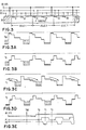
Es zeigen:
- Fig. 1 ein System, das in Ruhezustand durch leere Bits im seriellen Eingaberegister definiert ist,
- Fign. 2A bis 2F den Datenfluss, wenn der serielle-parallele-serielle Speicher in Zeilenadressierung betrieben wird,
- Fig. 3 drei Zellen, die in Ladungskopplungstechnik (CCD) ausgeführt im Weiterleitungsbetrieb betrieben werden.
- Fign. 3A bis 3D Energieniveaus zur Darstellung des Ladungsflusses in der in Fig. 3 gezeigten Struktur,
- Fig. 3E mehrere Wellenlinien zur Darstellung der Steuerspannung an jeder Elektrode in Fig. 3,
- Fig. 4 schematisch drei in Ladungskopplungstechnik ausgeführte Zellen, die im Haltebetrieb betrieben werden,
- Fign. 4A bis 4D Energieniveaus zur Darstellung des Ladungsflusses in der in Fig. 4 gezeigten Struktur,
- Fig. 4E mehrere Wellenlinien zur Darstellung der Steuerspannung an jeder Elektrode der in Fig. 4 gezeigten Struktur,
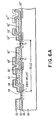
- Fig. 5 die horizontale Lage des seriellen-parallelen-seriellen zeilenadressierbaren Speichers der vorliegenden Erfindung,
- Fig. 6 in einer Vergrösserung der Fig. 5 die Struktur im Bereich der
Schnittlinie 6, - Fig. 6A einen vertikalen Schnitt entlang der
Schnittlinie 6A in Fig. 6, - Fig. 7 eine Vergrösserung der Fig. 5 in einem Bereich entlang der
Schnittlinien 7A und 7B, - Fig. 7A einen vertikalen Schnitt der vergrösserten horizontalen Auslegung der Fig. 7 entlang der
Schnittlinien 7A, - Fig. 7B einen vertikalen Schnitt der horizontalen Auslegung entlang der Schnittlinie 7B in Fig. 7,
- Fig. 1 zeigt schematisch eine serielle-parallele-serielle Konfiguration (SPS) mit einem
seriellen Eingangsregister 10, einemparallelen Mittelteil 12 und einemseriellen Ausgangsregister 14. Derartige Schaltungsanordnungen enthalten häufig auch noch einen Serien/Parallelwandler 16 und einen Parallel/Serienwandler 18. Leitungs-, Takt- und Ladeschaltungen für solche SPS-Konfigurationen sind allgemein bekannt und im Leit- undTaktschaltblock 20 schematisch dargestellt. Ebenfalls an sich bekannt sind Ladungsabfühl- und Verstärkerschaltungen mit Rücklaufverstärkern, wie sie allgemein durch denAbfrageverstärker 22 dargestellt sind. Ein Signal am Steuereingangsanschluss bestimmt, wann neue Daten am Dateneingangsanschluss oder vomAbfrageverstärker 22 zurückgeführte Daten in die erste Bitposition desseriellen Eingaberegisters 10 einzugeben sind. Auch im Umlaufbetrieb können Daten am Datenausgangsanschluss gleichzeitig genutzt werden.
- 1 shows a system which is defined in idle state by empty bits in the serial input register,
- Fig. 2A to 2F the data flow when the serial-parallel-serial memory is operated in row addressing,
- Fig. 3 three cells that are operated in charge coupling technology (CCD) in the forwarding mode.
- Fig. 3A to 3D energy levels for representing the charge flow in the structure shown in FIG. 3,
- 3E shows several wavy lines to illustrate the control voltage at each electrode in FIG. 3,
- 4 shows schematically three cells designed in charge coupling technology, which are operated in the holding mode,
- Fig. 4A to 4D energy levels for representing the charge flow in the structure shown in FIG. 4,
- 4E shows several wavy lines to illustrate the control voltage at each electrode of the structure shown in FIG. 4,
- 5 shows the horizontal position of the serial-parallel-serial line addressable memory of the present invention,
- 6 shows the structure in the region of the
section line 6 in an enlargement of FIG. 5, - 6A is a vertical section along the
section line 6A in Fig. 6, - 7 is an enlargement of FIG. 5 in an area along the
section lines 7A and 7B, - 7A is a vertical section of the enlarged horizontal design of FIG. 7 along the section lines 7A,
- 7B is a vertical section of the horizontal layout along the section line 7B in Fig. 7,
- 1 schematically shows a serial-parallel-serial configuration (PLC) with a
serial input register 10, a parallelmiddle part 12 and aserial output register 14. Such circuit arrangements often also contain a series /parallel converter 16 and a parallel /series converter 18 , Clock and charging circuits for such PLC configurations are generally known and are shown schematically in the control andclock switching block 20. Charge sensing and amplifier circuits with return amplifiers, as generally represented by thesense amplifier 22, are also known per se. A signal at the control input connection determines when new data at the data input connection or data returned by thequery amplifier 22 are to be input into the first bit position of theserial input register 10. Even in circulation mode, data on the data output connection can be used simultaneously.
Eine erfindungsgemässe Schaltung kann voll als standardmässige SPS-Schaltungskonfiguration betrieben werden. Auf bekannte Weise werden Datenbits seriell von links nach rechts in das serielle Eingangsregister 10 eingegeben. Wenn die gewünschte Anzahl von Bits in das Eingangsregister 10 eingegeben ist, werden sie parallel über den Serien/Parallelwandler 16 in eine erste Zeile des parallelen Mittelteiles 12 eingegeben. Dann werden neue Daten in das serielle Eingaberegister 10 eingegeben und wieder durch den Serien/Parallelwandler 16 in die erste Zeile des parallelen Mittelteiles 12 eingegeben, während die vorher dort stehenden Daten in die zweite Zeile gesetzt werden. Auf diese Weise wird der parallele Mittelteil 12 zeilenweise mit Daten gefüllt. Wenn die zuerst eingegebenen Daten die letzte Zeile des parallelen Mittelteiles 12 erreichen, werden sie parallel durch den Parallel/Serienwandler 18 in das serielle Ausgangsregister 14 gegeben. Hier werden Daten bitweise in den Abfrageverstärker 22 und von dort weiter an den Datenausgangsanschluss und an den angegebenen Eingang des Leit- und Taktschaltblockes 20 weitergeleitet. Im Umlaufbetrieb werden die Daten am Datenausgangsanschluss nicht benutzt, sondern die vom Abfrageverstärker 22 kommenden Bits werden über den Leit- und Taktschaltblock 20 wieder in das serielle Eingaberegister 10 eingegeben. Durch diesen dauernden Umlauf des Datenbitstromes wird ein Informationsverlust in den Ladungskopplungselementen verhindert.A circuit according to the invention can be operated fully as a standard PLC circuit configuration. In a known manner, data bits are entered serially into the serial input register 10 from left to right. When the desired number of bits have been entered into the
Es besteht im vorliegenden die Absicht darin, Daten auf bekannte Art einer SPS-Struktur umlaufen zu lassen, wie es oben beschrieben wurde. Ein Datensatz muss jedoch eingegeben und ausgegeben werden können wie schraffiert in Fig. 1 dargestellt. Zur besseren Beschreibung wurden die Bitpositionen in Fig. 1 bezeichnet. Die Anordnung enthält N-1 Zeilen im parallelen Mittelteil, von denen die erste Zeile die Z Bits speichert, während die N-1 Zeile die B Bits speichert. (M + 1) x N Bits werden insgesamt gespeichert, da die A Bits im seriellen Ausgaberegister gespeichert werden. Jede Spalte speichert einen gewünschten Datensatz, der aus den Datenbits A bis Z besteht. Die schraffierten Zellen zeigen die serielle Bahn, auf der ein Datensatz eingegeben oder ausgegeben wird.The intention here is to circulate data in a known manner in a PLC structure, as described above. However, a data record must be able to be entered and output as shown by hatching in FIG. 1. For better description, the bit positions have been designated in Fig. 1. The arrangement contains N-1 lines in the parallel central part, of which the first line stores the Z bits, while the N-1 line stores the B bits. (M + 1) x N bits are stored in total because the A bits are stored in the serial output register. Each column stores a desired data set, which consists of data bits A to Z. The hatched cells show the serial path on which a data record is entered or output.
Insbesondere der Datensatz 2, d. h. A2 B2 ... Z2, ist in Ruheposition gezeigt. Der Datensatz ist analog der zeilenadressierbaren Spalte einer herkömmlichen zeilenadressierbaren Struktur. In diesem Beispiel wurde das Eingaberegister 10 mit Nullbits gefüllt. Nach dem Erfindungsgedanken kann man die schraffierten Bits in folgender Reihenfolge auslesen: A0, A1, A2, B2 bis Z2 und die Nullbits, wie es im schraffierten Teil des Registers dargestellt ist. Während diese Bits am Datenausgangsanschluss ausgelesen werden, laufen sie auch durch den Leit- und Taktschaltblock 20 um, so dass am Ende der Operation genau die Konfiguration wieder hergestellt ist, die in Fig. 1 gezeigt ist. Jetzt kann man entweder einen anderen Datensatz, z. B. A3 bis Z3, adressieren oder die Erneuerung mit einer herkömmlichen SPS-Operation wieder aufnehmen. Während eine gewünschte Zeile adressiert wird, bleiben natürlich alle anderen Bits in den parallelen Kanälen inaktiv, d.h. sie werden nicht weitergeleitet.In particular,
In den schraffierten Teilen des Eingabe- und des Ausgaberegisters befinden sich noch (M+1) zusätzliche Bits, die zusammen mit dem nutzbaren Datensatz bewegt werden müssen, von den logischen Schaltungen des Systems jedoch ignoriert werden.In the hatched parts of the input and the output register there are (M + 1) additional bits that have to be moved together with the usable data record, but are ignored by the logic circuits of the system.
Das in den Fign. 2A bis 2F im einzelnen gezeigte Beispiel verwendet das in Fig. 1 dargestellte Ausführungsbeispiel, in dem die leeren oder Nullbits im Eingaberegister 10 stehen. Der Serien/Parallelwandler 16 und der Parallel/Serienwandler 18 aus Fig. 1 wurden der einfacheren Darstellung halber absichtlich weggelassen. Die Bezeichnung der Bits wurde aus demselben Grund geringfügig geändert.The in Figs. 2A to 2F, the example shown in detail uses the embodiment shown in FIG. 1, in which the empty or zero bits are in the
Unter Bezug auf Fig. 2A wird angenommen, dass der Datensatz Nr. 2, bestehend aus den Bits A, B, C, D bis Z die zu adressierende Zeile ist. Da es der dritte Datensatz ist, zeigt ein Zähler am Ausgangsanschluss im Benutzergerät, dass die Bits WO und W1 den ersten beiden Datensätzen entsprechen und daher nicht Teil der adressierten Zeile sind. Nach Darstellung in Fig. 2B ist also das Bit WO das erste ausgehende Bit, das auch in die erste Bitposition im seriellen Eingaberegister 10 geschrieben wird, wenn jedes Bit um eine Position verschoben wird. Fig. 2C zeigt die Situation, wenn jedes Bit um eine weitere Position verschoben wurde, wobei W1 ausgelesen und in die erste Bitposition in das serielle Register 10 gesetzt wird, während alle anderen Bits entsprechend um eine Position verschoben werden. In Fig. 2D ist gezeigt, wie das Auslesen der adressierten Zeile beginnt mit dem Auslesen von Bit A. Um die Situation besser darzustellen, in der dieselben Daten nicht umlaufen gelassen werden, wird ein neues Bit A mit der Bezeichnung A' an den Eingangsanschluss angelegt und in die erste Bitposition des Eingaberegisters 10 gesetzt. Alle Bits werden entsprechend verschoben wie vorher beschrieben.With reference to FIG. 2A, it is assumed that data record No. 2, consisting of bits A, B, C, D to Z, is the line to be addressed. Since it is the third data record, a counter at the output connection in the user device shows that bits WO and W1 correspond to the first two data records and are therefore not part of the addressed line. As shown in FIG. 2B, the bit WO is the first outgoing bit that is also written into the first bit position in the
Dieser Ausschiebeprozess des gewünschten Datensatzes geht weiter, während die neuen Bits eingeschoben werden, bis der in Fig. 2E gezeigte Zustand erreicht ist. Hier wurde das letzte Bit (Z) an den Datenausgangsanschluss gegeben und das neue Bit in die erste Position des Eingaberegisters 10 gesetzt. An diesem Punkt sind die Daten fertig ausgelesen, obwohl noch einige weitere Zyklen erforderlich sind, um die Datenbits in ihre Ausgangsposition zurückzuschieben. Das ist in Fig. 2F gezeigt, wo alle Datenbits wieder in ihrer ursprünglichen Position stehen und die Bits A', B', C', D' bis Z' ihre ursprünglichen Bits ohne die Strichbezeichnung in Fig. 2A ersetzt haben. Auf diese Weise arbeitet ein serieller-paralleler-serieller Speicher im Zeilenadressbetrieb, wo jeder gewünschte Datensatz beliebig adressiert werden kann. Der Vorteil dieser Struktur besteht in der offensichtlichen Reduzierung der Latenzzeit. Wenn der Datensatz Z der Fig. 1 gewünscht wird, muss man im herkömmlichen SPS-Betrieb warten, bis die ganze Gruppe adressiert ist. Durch das gezeigte LA-SPS-Betriebsverfahren beläuft sich die Latenzzeit im ungünstigsten Falle auf die Schiebezeit von M Bits, wenn irgendein Datensatz gewünscht wird. Für den in Fig. 1 gezeigten Fall ist die Latenzzeit nur genauso gross, wie die Schiebezeit für die Bits AO und A1. Eine weitere Verschiebung muss jedoch vorgenommen werden, um die Daten wieder in ihre ursprüngliche Konfiguration zu setzen und die Operation zu beenden.This process of pushing out the desired data set continues while the new bits are inserted until the state shown in FIG. 2E is reached. Here the last bit (Z) was given to the data output connection and the new bit was set in the first position of the
Eine beispielhafte Struktur zur Ausführung dieser Funktion ist in Fig. 3 gezeigt, wo in einem P-leitenden Substrat 30 P+ Bereiche 31, 32, 33, 34, 35, 36 und 37 durch Ionenimplantation geschaffen wurden. Einzelheiten einer jeden Zelle sind an der Zelle 1, 2 und 3 gezeigt. Zu jeder Zelle gehören drei Elektroden, nämlich eine Gleichspannungs-Steuerleitung, eine Phase 1 (P1) und eine Phase 2 (P2). Durch Anlegen drei verschiedener Potentialpegel an die drei verschiedenen Elektroden können bekanntlich in jeder Zelle drei verschiedene Energieniveaus geschaffen werden. Durch die zusätzliche Ionenimplantation unter einem Teil der Gateelektrode können jedoch unter dieser Gateelektrode zwei Energieniveaus geschaffen werden. Durch die lonenimplantation 31 unter einem Teil der Gateelektrode für die Phase 1 kann man also zwei separate Energieniveaus unter dieser Gateelektrode schaffen. Entsprechendes gilt für lonenimplantation 32 unter der Gateelektrode der Phase 2. Unter der Gateelektrode für die Gleichspannungs-Steuerleitung liegt keine lonenimplantation, so dass hier nur ein Energieniveau erzeugt werden kann. Insgesamt bieten die drei Elektroden die Möglichkeit, fünf Energieniveaus in jeder Zelle zu erzeugen. Fig. 3E zeigt die angelegten Potentialpegel, während die Fign. 3A bis 3D die Weiterleitung der Ladung durch die Zellen darstellen.An exemplary structure for performing this function is shown in FIG. 3, where P +
Die Fign. 3A bis 3E zeigen den Zustand, in dem Ladung durch die Schaltungsanordnung weitergeleitet wird. Dieser Vorgang läuft während der SPS-Operation in jeder Zeile ab. Die Fign. 3A bis 3E zeigen den Zustand der adressierten Zeile im Zeilenadressierbetrieb. Die zur Zeit too angelegten Potentialpegel sind in Fig. 3E dargestellt. Die Gleichspannungs-Steuerleitung sowie die Leitung für die Phase 1 befinden sich auf einem niedrigen Pegel, die Leitung für die Phase 2 auf einem hohen. Das resultiert in der in Fig. 3A gezeigten Potentialtopfkonfiguration. In dem in Fig. 3A gezeigten Beispiel wird eine binäre 1 in Zelle 1 und in der vorhergehenden Zelle gespeichert, während in den Zellen 2 und 3 Nullen gespeichert werden. Zur Zeit to wird die Gleichspannungs-Steuerleitung auf einen hohen Pegel gebracht, während der Signalpegel auf den Leitungen für die Phasen 1 und 2 nicht verändert wird. Dadurch werden die Potentialtöpfe anders angeordnet, und zwar so wie es in Fig. 3B gezeigt ist. Zur Zeit t, wurde die Elektrode für die Phase 1 auf einen hohen Signalpegel gebracht, während die Elektrode für die Phase 2 auf einen niedrigen Pegel gebracht wurde und die Steuerleitung auf einem hohen Pegel gehalten wurde. Das führt zu der in Fig. 3C gezeigten Anordnung der Potentialtöpfe und einer Ladungs- übertragung in der in Fig. 3C durch die Pfeile angezeigten Richtung.The figures 3A to 3E show the state in which charge is passed through the circuit arrangement. This process takes place in every line during the PLC operation. The figures 3A to 3E show the state of the addressed line in the line addressing mode. The potential levels applied at time t oo are shown in FIG. 3E. The DC voltage control line and the line for
Zur Zeit t2 wird die Gleichspannungs-Steuerleitung auf einem hohen Pegel gehalten, während die Leitung für die Phase 1 auf einem niedrigen und die Leitung für die Phase 1 auf einen hohen Pegel gebracht wurde. Das führt zu der in Fig. 3D gezeigten Verteilung der Potentialtöpfe. Die Ladungsübertragung ist im wesentlichen abgeschlossen, wobei die Zelle 1 eine binäre 1 enthält, die vorher in der vorhergehenden Zelle stand, die Zelle 2 ebenfalls eine binäre 1, die vorher in der Zelle 1 stand und die Zelle 3 die fette Null enthält, die vorher in der Zelle 2 stand.At time t 2 , the DC control line is held at a high level, while the line for
Fig. 4 zeigt die gleiche Struktur wie Fig. 3. Im Zusammenhang mit den Fign. 4 und 4A bis 4E wird der Zustand der inaktiven Leitungen während des Zeilenadressierbetriebes gezeigt. Die Anfangszustände der Steuerleitungen in Fig. 4E sind mit denen der Fig. 3E zur Zeit too identisch. Ausserdem werden identische binäre Daten gemäss Darstellung in Fig. 4A gespeichert, wie in Fig. 3A. Somit ist Fig. 4A also mit Fig. 3A identisch. Zur Zeit to hat sich gegenüber dem Zustand zur Zeit too nichts geändert, und daher sind auch die Potentialtöpfe in Fig. 4B mit denen in Fig. 4A absolut identisch.FIG. 4 shows the same structure as FIG. 3. In connection with FIGS. 4 and 4A through 4E, the state of the inactive lines during row addressing operation is shown. The initial states of the control lines in FIG. 4E are identical to those of FIG. 3E at time t oo . In addition, identical binary data are stored as shown in FIG. 4A, as in FIG. 3A. Thus, FIG. 4A is identical to FIG. 3A. At time t o , nothing has changed from the state at time t oo , and therefore the potential wells in FIG. 4B are absolutely identical to those in FIG. 4A.
Zur Zeit t, ist in Fig. 4E im Gegensatz zur Fig. 3E festzustellen, dass die Gleichspannungs-Steuerleitung auf einem niedrigen Signalpegel gehalten wird, während die Leitung der Phase 1 auf einen hohen und die der Phase 2 auf einen niedrigen Signalpegel gebracht wurden. Das führt zu der in Fig. 4C gezeigten Verteilung der Potentialtöpfe. Der Potentialtopf, der eine Ladung enthält, die Information darstellt, wird auf einen höheren Signalpegel angehoben, und der Teil der binären 1-Ladung, der die Tiefe des Topfes X überschreitet, «schwappt zurück» in den vorhergehenden Potentialtopf. Zur nachfolgenden Zeit t2 wird die Leitung für die Phase 1 auf einen niedrigen Signalpegel gebracht, während die Leitung der Phase 2 auf einen hohen Signalpegel gebracht und so die Potentialtopfanordnung erzeugt wird, die in Fig. 4D gezeigt ist, die mit der Fig. 4B identisch ist. Dadurch kann sich die Anordnung der Potentialtöpfe zwischen den Anordnungen der Fign. 4C und 4D vorwärts und rückwärts verändern und auf diese Weise die Information in allen nicht gewählten Leitungen «stationär» gehalten werden. Dieser Zustand herrscht auf allen Zeilen vor, auf denen die Gleichspannungs-Steuerleitung auf einem niedrigen Potential gehalten wird. Die Gleichspannungs-Steuerleitung übernimmt also eine Sperrfunktion und kann bei derartiger Verwendung auch als Sperrleitung bezeichnet werden. Die Adresswahlschaltung gestattet ein Hochschalten des Signalpegels auf der Sperrleitung nur in der gewählten Zeile, während er auf allen anderen Zeilen niedrig gehalten wird.At time t, in contrast to FIG. 3E, it can be seen in FIG. 4E that the DC control line is kept at a low signal level, while the
Im Zusammenhang mit Fig. 5 wird eine Schaltung beschrieben, die für die Ausführung des SPS-Betriebes sowie des Zeilenadressierbetriebes geeignet ist. Allgemein bekannte Operationen wie Übertragungen innerhalb eines seriellen Registers, Übertragungen innerhalb eines parallelen Registers und Serien/Parallelumsetzungen oder Parallel/Serienumsetzungen sowie andere Einzelheiten der Ladungserzeugung und -abfühlungen werden nicht im einzelnen beschrieben, da sie allgemein bekannt sind.A circuit is described in connection with FIG. 5 which is suitable for executing the PLC operation and the line addressing operation. Commonly known operations, such as transfers within a serial register, transfers within a parallel register and serial / parallel conversions or parallel / serial conversions, as well as other details of charge generation and sensing are not described in detail since they are generally known.
Ein Gesichtspunkt der in Fig. 5 gezeigten Konfiguration ist die Verwendung von mittels Gleichstrom gesteuerten Ladungskopplungselementen für die zeilenadressierbare SPS-Speicheranordnung. Solche Ladungskopplungselemente brauchen eine Gleichstrom-Steuerleitung für jeden parallelen Kanal, können aber mit gemeinsamen Taktleitungen für alle parallelen Kanäle betrieben werden. Das ist insofern ein wichtiger Punkt, als hierdurch eine sehr dichte Schaltungsanordnung ermöglicht wird. Das bedeutet, dass sämtliche Schaltungs- und Raumeinsparungen direkt dem Konzept der zeilenadressierbaren seriellen-parallelen-seriellen Speicheranordnung zuzuschreiben sind.One aspect of the configuration shown in FIG. 5 is the use of DC controlled charge coupling elements for the line addressable PLC memory array. Such charge coupling elements require a DC control line for each parallel channel, but can be operated with common clock lines for all parallel channels. This is an important point in that it enables a very dense circuit arrangement. This means that all circuit and space savings can be directly attributed to the concept of the row-addressable serial-parallel-serial memory arrangement.
Fig. 5 zeigt primär den Lauf der Takt- und Steuerleitungen. Das serielle Eingaberegister 10, der parallele Mittelteil 12 und das serielle Ausgaberegister 14 sind wieder genauso numeriert wie in den vorhergehenden Zeichnungen. Das serielle Eingaberegister 10 empfängt eine Eingabe in einem Erzeugungsteil und es empfängt die Verbindung der Elektroden für die Phasen 1 und die Phase 2. Zusätzlich zum herkömmlichen zweiphasigen seriellen Eingaberegister sind hier die Sperrleitungen (S1) vom Kanalwähler vorhanden. Hierbei handelt es sich um die oben beschriebenen Gleichstrom-Steuerleitungen, die während der Zeilenadressierung selektiv aktiviert werden müssen. Datenbits werden im SPS-Betrieb in allen seriellen Eingaberegistern und im Zeilenadressierbetrieb selektiv übertragen, abhängig von der adressierten Zeile, wie es beispielsweise im Zusammenhang mit Fig. 1 beschrieben wurde. Die beiden Zellengruppen des seriellen Eingaberegisters 10 sind genauso angeordnet, wie es oben im Zusammenhang mit den Fign. 3 und 4 beschrieben wurde.Fig. 5 shows primarily the running of the clock and control lines. The
Im parallelen Teil sind die eine gewählte und alle anderen Zellenspaltungen genauso angeordnet, wie es oben im Zusammenhang mit den Fign. 3 und 4 beschrieben wurde. Die Verbindung der parallelen Kanaltaktleitungen für die Phase 1 und 2 ist besonders gezeigt. Die zeitliche Beziehung der Phase 1 zur Phase 2 im seriellen und parallelen Teil wird wunschgemäss und abhängig von der jeweiligen Art gewählt, in der die Serien/Parallelumwandlung erfolgen soll (siehe Fign. 3E und 4E). Insbesondere sind die parallelen Kanalsteuerleitungen (S2) zu beachten, die an jeder Spalte entlanglaufen. Sie entsprechen den Gleichspannungs-Steuerleitungen, die im Zusammenhang mit den Fign. 3 und 4 beschrieben wurden. Durch Anordnung einer derartigen Leitung in jeder Spalte im parallelen Teil kann man im Zeilenadressierbetrieb jede gewählte Spalte aktivieren, während alle anderen gesperrt werden. Diese parallelen Kanalsteuerleitungen werden durch den Kanaldecodierer/wähler gesteuert, der eine Kanaladresse empfängt. Der Kanaldecodierer/wähler steuert auch die seriellen Kanalsteuerleitungen (S3) im seriellen Ausgaberegister 14. Nachdem also die Bits von der letzten Zeile des parallelen Mittelteiles 12 (entweder parallel im SPS-Betrieb oder bitweise wie im Zeilenadressbetrieb) übertragen sind, werden sie seriell aus dem seriellen Ausgaberegister 14 durch die Taktimpulse der Phase 1 und der Phase 2 über den Detektor an den Ausgabeanschluss ausgeschoben.In the parallel part, the one selected and all other cell divisions are arranged exactly as described above in connection with FIGS. 3 and 4 has been described. The connection of the parallel channel clock lines for
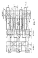
Fig. 6 ist eine vergrösserte Darstellung der in Fig. 5 gezeigten Struktur im Bereich der Schnittlinie 6. In Fig. 6 sind Teile von zwei parallelen Spalten dargestellt. Das Substrat 60 ist typischerweise mit P-leitenden Verunreinigungen dotiert. Die Herstellung von Ladungskopplungselementen mit N-leitenden Substraten ist natürlich auch bekannt. lonenimplantationen sowie die verschiedenen Elektroden aus Polysilizium und Metall werden in der gezeigten Anordnung mit bekannter Lithographietechnik hergestellt. Die Taktleitungen für die Phase 1 werden mit den Polysiliziumelektroden 62 und 64 gebildet, wobei die Elektrode 62 mit Poly 1 und die Elektrode 64 mit Poly 2 bezeichnet wird. Diese Bezeichnung wurde festgelegt in der Reihenfolge, in der die verschiedenen Polysiliziumelektroden mit den verschiedenen dazwischen liegenden Isolierschichten aus Siliziumdioxid ausgebildet werden. Die Taktleitungen der Phase 2 werden durch die Polysiliziumelektroden 62' und 64' gebildet. Der oberste Schichtleiter (im allgemeinen aus Metall gebildet) ist die Sperrleitung 66 für eine Spalte und die Sperrleitung 66' für die andere Spalte. Die erste Spalte ist von der zweiten Spalte durch eine vertiefte Oxidisolation 67' getrennt. Die erste Spalte ist von der anderen benachbarten Spalte durch die Oxidvertiefung 67 getrennt, während die zweite gezeigte Spalte von der nächsten Nachbarspalte durch das vertiefte Oxid 67" getrennt ist. Die Oxidisolation sowie andere Isolationsarten zwischen den Spalten sind zwar allgemein bekannt, für die vorliegende Erfindung jedoch besonders nützlich, als die Gesamtstruktur in allen möglichen Hinsichten zwar der bekannten SPS-Anordnung entspricht, sich jedoch von ihr durch die zusätzliche hier beschriebene Zeilenadressiereinrichtung unterscheidet.FIG. 6 is an enlarged illustration of the structure shown in FIG. 5 in the area of the
Fig. 6A zeigt einen vertikalen Schnitt durch die Struktur der Fig. 6 entlang der Schnittlinie 6A. Fig. 6A ist eine detaillierte Darstellung des im Zusammenhang mit den Fign. 3 und 4 beschriebenen Schemas. Auf dem Substrat 60 werden die verschiedenen Elektroden 62, 64 und 66 sowie die lonenimplantationen 68, 68' usw. ausgebildet. Bei einem P-leitenden Substrat sind die lonenimplantationen P+-leitend. Die Sperrelektrode ist im allgemeinen ein Metall, dreifache Polystrukturen sind jedoch ebenso bekannt. Die Elektrode 66 kann genausogut aus Polysilizium hergestellt sein. Die verschiedenen Elektroden sowie das Substrat sind in geeigneter Weise voneinander durch Siliziumdioxid isoliert.FIG. 6A shows a vertical section through the structure of FIG. 6 along the
Eine typische Zelle, entsprechend z.B. der Zelle 1 in den Fign. 3 und 4, ist in Fig. 6A gezeigt. Die Elektrode für die Phase 1 (P1) enthält Poly 1 (62) und Poly 2 (64) und zeigt deutlich die in den Fign. 3 und 4 nur schematisch dargestellte Verbindung der beiden Elektroden. Unter der Poly 2 Elektrode 64 wurde die lonenimplantation 68 ausgebildet.A typical cell,
Der Anschluss für die Phase 2 (PZ) ist an die Elektrode 62' (Poly 1) und 64' (Poly 2) angeschlossen, wobei letztere über der lonenimplantation 68' ausgebildet ist. Der letzte Anschluss für diese Zelle ist die Gleichstrom-Steuerelektrode 66 (Sperrelektrode). Die dünne Oxidschicht 69 braucht nicht gleiehmässig zu sein, so kann beispielsweise die erste Dicke t, unter den Polysiliziumelektroden 62 und 64 in der Grössenordnung von 5x10⁻⁸m (500Ä) liegen. Eine zweite Dicke t2 unter den metallischen Steuerelektroden (Speielektroden) kann in der Grössenordnung von 10-7 m (1000 Å) liegen. Fig. 7 ist eine Vergrösserung der Darstellung in Fig. 5 im Bereich der Schnittlinien 7A und 7B. Das Substrat wurde mit der Bezugszahl 70 bezeichnet. Der in Fig. 7 vergrössert dargestellte Bereich enthält einen Teil des parallelen Kanales, einen Teil des Parallel/Serienwandlers und einen Teil des seriellen Kanales. Entlang der Schnittlinie 7B ist in Fig. 7 ein Teil des parallelen Kanales, ein Teil des Parallel/Serienwandlers und ein Teil des seriellen Kanales gezeigt. In Fig. 7 ist ausserdem entlang der Schnittlinie 7A nur ein Teil des seriellen Kanales gezeigt.The connection for phase 2 (PZ) is connected to the electrode 62 '(poly 1) and 64' (poly 2), the latter being formed above the ion implantation 68 '. The last connection for this cell is the DC control electrode 66 (blocking electrode). The
In dem Teil des in Fig. 7, 7A und 7B gezeigten parallelen Kanales werden die Taktleitungen für die Phase 2 gebildet durch die Elektroden 82 und 84, wobei die Elektrode 82 Poly 1 ist und die Elektrode 84 Poly 2. Im Übergangs- oder Wandlerbereich werden die Elektroden 82' und 84' für die Taktphase 1 gebildet durch Poly 1 bzw. Poly 2. Im seriellen Kanal werden die Elektroden 72 und 74 für die Taktphase 2 gebildet durch Poly 1 bzw. Poly 2. Die parallelen Kanalsteuerleitungen 76 (Sperrleitungen) laufen vom parallelen Kanal über den seriellen Kanal, beeinflussen diesen jedoch nicht, weil sie vom Substrat durch eine dicke Oxidschicht getrennt sind. Die seriellen Steuerelektroden 77 jedoch liegen nur im seriellen Kanalbereich und haben dieselbe Sperr- oder Übertragungsfunktion, die oben für die parallelen Kanalsteuerleitungen beschrieben wurden.In the part of the parallel channel shown in FIGS. 7, 7A and 7B, the clock lines for
Fig. 7A zeigt einen vertikalen Schnitt durch die in Fig. 7 gezeigte Struktur entlang der Schnittlinie 7A. Es ist ein Teil des seriellen Ausgaberegisters dargestellt (das serielle Eingaberegister hat natürlich genauso aufgebaute Zellen). Im P-leitenden Substrat sind mehrere P+-leitende lonenimplantationen 71, 71', 71", 71'" ausgebildet. Durch Siliziumdioxid in geeigneter Weise voneinander isoliert liegen die Poly 1 Elektrode 72 und die Poly 2 Elektrode 74. Die parallelen Kanalsteuerleitungen 76 sind vom Substrat nicht durch ein dickes Oxid, sondern auch durch die entsprechenden Polysiliziumelektroden getrennt, und haben daher keinen Einfluss auf die Weiterleitung der Ladung. Die seriellen Leiter 77 jedoch sind vom Substrat nur durch ein dünnes Oxid getrennt. Das die Metallsteuerelektroden vom Substrat trennende dicke Oxid kann etwa 10-'7m (1000Ä) dick sein, das die Polyelektroden vom Substrat trennende dünne Oxid etwa 5x 10⁻⁸m (500A). Die in Fig. 7Agezeigte typische Zelle hat als Steuerelektrode die seriellen Steuerelektroden 77. Die Leitung für die Taktphase 2 ist sowohl an die Poly 1 Elektrode 72 als auch an die Poly 2 Elektrode 74 angeschlossen, die im wesentlichen über der lonenimplantation 71 liegt. Die Steuerleitung für die Phase 1 ist an die Poly 1 Elektrode 72 und die Poly 2 Elektrode 74 angeschlossen, die im wesentlichen über die Ionenimplantation 71' liegt. In dieser Schaltungsanordnung wird die Ladung von rechts nach links weitergeleitet.FIG. 7A shows a vertical section through the structure shown in FIG. 7 along the
Fig. 7B zeigt einen Schnitt durch die in Fig. 7 gezeigte Struktur entlang der Schnittlinie 7B. Im parallelen Kanalteil werden die Elektroden für die Taktphase 2 durch die Poly 1 Elektrode 82 und die Poly 2 Elektrode 84 gebildet, die im wesentlichen über der lonenimplantation 88 liegt.FIG. 7B shows a section through the structure shown in FIG. 7 along the section line 7B. In the parallel channel part, the electrodes for the
Die Elektroden für die Taktphase 1 werden durch die teilweise gezeigte Poly 1 Elektrode 82 mit einer anderen Poly 2 Elektrode gebildet (nicht dargestellt). Die Steuerelektrode 76 bildet den Sperrkontakt für die gezeigte Zelle im parallelen Kanalteil. Im Wandlerteil werden die Elektroden für die Taktphase 1 durch die Poly 1 Elektrode 82' und die Poly 2 Elektrode 84' gebildet, die im wesentlichen über der lonenimplantation 88' liegt. Der serielle Kanalteil ist besser in Fig. 7A dargestellt. Rechts vom seriellen Kanalteil ist in Fig. 7B eine typische vertiefte Oxidisolation 90 dargestellt. Das Substrat wurde in Fig. 7B mit der Nummer 80 bezeichnet.The electrodes for
Vorstehend wurde eine zweiphasige Ausführung der Erfindung beschrieben. Gemeinsame Taktleitungen werden für jede Speicherspalte benutzt, wie es bei SPS-Schaltungsanordnungen üblich ist. Damit wird die hohe Dichte der SPS-Schaltungen erhalten. Für die erhöhte Flexibilität der Zeilenadressierung ist lediglich eine Gleichspannungs-Steuerleitung für jeden Kanal erforderlich. Die Verwendung eines Leiters auf einer dritten Ebene für die Gleichstrom-Steuerelektroden (Sperrelektroden) ist keine wesentliche Belastung für eine vorhandene SPS-Schaltung. Da eine Metallebene gewöhnlich als integrierter Teil bei der Herstellung eines Ladungskopplungselementes mit zwei selbst ausrichtenden Polysiliziumelektroden ist, ist die Verwendung von Metall für die Gleichstrom-Steuerelektroden sehr bequem. Die Verwendung von Metalielektroden auf dünnem Oxid ist jedoch zuverlässiger, wenn das dünne Oxid unter dem Metall dicker ist als unter dem Polysilizium, weil die Gleichspannungs-Steuerelektroden das Energieniveau unter sich nur ungefähr halb so viel zu ändern brauchen, wie die Elektroden unter dem Polysilizium. Durch eine dickere Oxidschicht unter den Metallelektroden verursacht die gleiche angelegte Gleichspannung unter diesen Metallelektroden eine geringere Energieänderung. Andererseits könne kleinere Gleichspannung an die Metallelektroden angelegt werden, so dass überall das dünne Oxid eine gleichmässige Dicke haben kann. Die relativen Spannungspegel für die Taktphasen 1 und 2 und die Gleichspannungs-Steuerelektroden sind an sich bekannt, mit denen die gezeigten Potentialbarrieren unter den verschiedenen Steuerelektroden errichtet werden. Der niedrige Pegel für die beiden Taktsignale Phase 1 und Phase 2 muss beispielsweise eine ausreichend hohe Spannung haben, so dass die Richtungsbarriere unter den lonenimplantationen nicht diejenige unter den Gleichspannungs-Steuerelektroden überschreitet. Der Richtungssinn kann in zweiphasigen Ladungskopplungselementen bekanntlich auch mit anderen Techniken als der lonenimplantation erreicht werden, beispielsweise durch eine Versetzung von dünnem und dickem Oxid.A two-phase embodiment of the invention has been described above. Common clock lines are used for each memory column, as is common in PLC circuitry. This maintains the high density of the PLC circuits. For the increased flexibility of row addressing, only one DC control line is required for each channel. The use of a third level conductor for the DC control electrodes (blocking electrodes) is not a significant burden for an existing PLC circuit. Since a metal plane is usually an integrated part in the manufacture of a charge coupling element with two self-aligning polysilicon electrodes, the use of metal for the DC control electrodes is very convenient. However, the use of metal electrodes on thin oxide is more reliable if the thin oxide is thicker under the metal than under the polysilicon, because the DC control electrodes need to change the energy level between them only about half as much as the electrodes under the polysilicon. Due to a thicker oxide layer under the metal electrodes, the same DC voltage applied under these metal electrodes causes less energy change. On the other hand, smaller DC voltages can be applied to the metal electrodes, so that the thin oxide can have a uniform thickness everywhere. The relative voltage levels for clock phases 1 and 2 and the DC voltage control electrodes are known per se, with which the potential barriers shown are erected under the various control electrodes. The low level for the two
Bisher wurde die Modifikation einer SPS-Schaltungsanordnung zu einer zeilenadressierbaren SPS-Schaltungsanordnung beschrieben. Es kann aber auch eine zeilenadressierbare Schaltungsanordnung so modifiziert werden, dass sie eine SPS-Funktion enthält.So far, the modification of a PLC circuit arrangement to a line-addressable PLC circuit arrangement has been described. However, a line-addressable circuit arrangement can also be modified in such a way that it contains a PLC function.
Claims (6)
Applications Claiming Priority (2)
| Application Number | Priority Date | Filing Date | Title |
|---|---|---|---|
| US974634 | 1978-12-29 | ||
| US05/974,634 US4228526A (en) | 1978-12-29 | 1978-12-29 | Line-addressable serial-parallel-serial array |
Publications (3)
| Publication Number | Publication Date |
|---|---|
| EP0012840A2 EP0012840A2 (en) | 1980-07-09 |
| EP0012840A3 EP0012840A3 (en) | 1980-09-17 |
| EP0012840B1 true EP0012840B1 (en) | 1983-02-23 |
Family
ID=25522282
Family Applications (1)
| Application Number | Title | Priority Date | Filing Date |
|---|---|---|---|
| EP79104586A Expired EP0012840B1 (en) | 1978-12-29 | 1979-11-19 | Line-addressable memory with serial-parallel-serial configuration |
Country Status (5)
| Country | Link |
|---|---|
| US (1) | US4228526A (en) |
| EP (1) | EP0012840B1 (en) |
| JP (1) | JPS5826117B2 (en) |
| DE (1) | DE2964922D1 (en) |
| IT (1) | IT1165432B (en) |
Families Citing this family (6)
| Publication number | Priority date | Publication date | Assignee | Title |
|---|---|---|---|---|
| NL8104102A (en) * | 1981-09-04 | 1983-04-05 | Philips Nv | LOAD-COUPLED DEVICE. |
| US4720819A (en) * | 1983-12-30 | 1988-01-19 | Texas Instruments Incorporated | Method and apparatus for clearing the memory of a video computer |
| JPS61227U (en) * | 1984-06-06 | 1986-01-06 | 富士電機株式会社 | Connection device between bushing current transformer and conductor |
| JPH0770704B2 (en) * | 1989-05-25 | 1995-07-31 | 日本電気株式会社 | Charge transfer device and driving method thereof |
| US5519413A (en) * | 1993-11-19 | 1996-05-21 | Honeywell Inc. | Method and apparatus for concurrently scanning and filling a memory |
| JP2020141029A (en) * | 2019-02-27 | 2020-09-03 | 株式会社東芝 | Solid-state imaging device |
Family Cites Families (10)
| Publication number | Priority date | Publication date | Assignee | Title |
|---|---|---|---|---|
| AU461729B2 (en) * | 1971-01-14 | 1975-06-05 | Rca Corporation | Charge coupled circuits |
| US3720922A (en) * | 1971-03-17 | 1973-03-13 | Rca Corp | Charge coupled memory |
| US3967254A (en) * | 1974-11-18 | 1976-06-29 | Rca Corporation | Charge transfer memory |
| US3944990A (en) * | 1974-12-06 | 1976-03-16 | Intel Corporation | Semiconductor memory employing charge-coupled shift registers with multiplexed refresh amplifiers |
| US4024512A (en) * | 1975-06-16 | 1977-05-17 | Fairchild Camera And Instrument Corporation | Line-addressable random-access memory |
| DE2620973A1 (en) * | 1975-06-30 | 1977-01-27 | Ibm | SEMI-CONDUCTOR CIRCUIT FOR FET SUBSTRATE PRE-VOLTAGE GENERATION |
| US4011548A (en) * | 1975-07-02 | 1977-03-08 | Burroughs Corporation | Three phase charge-coupled device memory with inhibit lines |
| DE2543023C3 (en) * | 1975-09-26 | 1981-07-09 | Siemens AG, 1000 Berlin und 8000 München | Storage arrangement with modules from charge displacement storage |
| US4165541A (en) * | 1977-12-12 | 1979-08-21 | Fairchild Camera And Instrument Corporation | Serial-parallel-serial charge-coupled device memory having interlacing and ripple clocking of the parallel shift registers |
| JPS54150945A (en) * | 1978-05-18 | 1979-11-27 | Matsushita Electric Ind Co Ltd | Charge coupling element |
-
1978
- 1978-12-29 US US05/974,634 patent/US4228526A/en not_active Expired - Lifetime
-
1979
- 1979-11-19 DE DE7979104586T patent/DE2964922D1/en not_active Expired
- 1979-11-19 EP EP79104586A patent/EP0012840B1/en not_active Expired
- 1979-11-30 JP JP54154542A patent/JPS5826117B2/en not_active Expired
- 1979-12-18 IT IT28128/79A patent/IT1165432B/en active
Also Published As
| Publication number | Publication date |
|---|---|
| JPS5826117B2 (en) | 1983-05-31 |
| EP0012840A2 (en) | 1980-07-09 |
| US4228526A (en) | 1980-10-14 |
| IT1165432B (en) | 1987-04-22 |
| DE2964922D1 (en) | 1983-03-31 |
| EP0012840A3 (en) | 1980-09-17 |
| JPS5593590A (en) | 1980-07-16 |
| IT7928128A0 (en) | 1979-12-18 |
Similar Documents
| Publication | Publication Date | Title |
|---|---|---|
| DE2619849C3 (en) | Memory in integrated circuit technology | |
| DE2604449C3 (en) | Analog-to-digital converter | |
| DE2403019C2 (en) | ||
| DE2748536C2 (en) | ||
| DE3937068C2 (en) | Dynamic semiconductor memory device | |
| DE3539234C2 (en) | EPROM memory matrix with symmetrical elementary MOS cells and method for writing into the memory | |
| DE2551797B2 (en) | Charge coupled circuit | |
| DE2261786C3 (en) | ||
| DE3243565C2 (en) | ||
| DE2311994A1 (en) | LATENCY IMAGE STORAGE | |
| DE2261786B2 (en) | Fixed-value storage unit | |
| DE69332966T2 (en) | Semiconductor memory device | |
| DE2646301C3 (en) | Charge coupled semiconductor device | |
| DE2738678C3 (en) | Monolithically integrated storage cell | |
| EP0012840B1 (en) | Line-addressable memory with serial-parallel-serial configuration | |
| DE2528316A1 (en) | SIGNAL PROCESSING ARRANGEMENT FORMED BY A CHARGE TRANSFER DEVICE | |
| EP0012841B1 (en) | Row-column-addressable memory with serial-parallel-serial configuration | |
| WO2006029594A1 (en) | Semiconductor memory element | |
| DE2629329A1 (en) | CCD SLIDING REGISTER | |
| DE4406459A1 (en) | Integrated semiconductor circuit device with memory cell arrangement | |
| DE2543023C3 (en) | Storage arrangement with modules from charge displacement storage | |
| DE2537194A1 (en) | STACKED STORAGE WITH CHARGE-COUPLING TECHNOLOGY AND PROCESS FOR ITS REFRESHMENT | |
| EP1625591B1 (en) | Integrated memory circuit arrangement in particular a uniform-channel-programming flash memory | |
| DE2702830C2 (en) | ||
| DE2439986C3 (en) | Solid state memory |
Legal Events
| Date | Code | Title | Description |
|---|---|---|---|
| PUAI | Public reference made under article 153(3) epc to a published international application that has entered the european phase |
Free format text: ORIGINAL CODE: 0009012 |
|
| AK | Designated contracting states |
Designated state(s): DE FR GB NL SE |
|
| PUAL | Search report despatched |
Free format text: ORIGINAL CODE: 0009013 |
|
| AK | Designated contracting states |
Designated state(s): DE FR GB NL SE |
|
| 17P | Request for examination filed |
Effective date: 19801007 |
|
| GRAA | (expected) grant |
Free format text: ORIGINAL CODE: 0009210 |
|
| AK | Designated contracting states |
Designated state(s): DE FR GB NL SE |
|
| PG25 | Lapsed in a contracting state [announced via postgrant information from national office to epo] |
Ref country code: NL Effective date: 19830223 |
|
| REF | Corresponds to: |
Ref document number: 2964922 Country of ref document: DE Date of ref document: 19830331 |
|
| ET | Fr: translation filed | ||
| NLV1 | Nl: lapsed or annulled due to failure to fulfill the requirements of art. 29p and 29m of the patents act | ||
| PG25 | Lapsed in a contracting state [announced via postgrant information from national office to epo] |
Ref country code: SE Effective date: 19831120 |
|
| PGFP | Annual fee paid to national office [announced via postgrant information from national office to epo] |
Ref country code: DE Payment date: 19931118 Year of fee payment: 15 |
|
| EUG | Se: european patent has lapsed |
Ref document number: 79104586.7 Effective date: 19850607 |
|
| PG25 | Lapsed in a contracting state [announced via postgrant information from national office to epo] |
Ref country code: DE Effective date: 19950801 |
|
| PGFP | Annual fee paid to national office [announced via postgrant information from national office to epo] |
Ref country code: FR Payment date: 19951107 Year of fee payment: 17 |
|
| PGFP | Annual fee paid to national office [announced via postgrant information from national office to epo] |
Ref country code: GB Payment date: 19961028 Year of fee payment: 18 |
|
| PG25 | Lapsed in a contracting state [announced via postgrant information from national office to epo] |
Ref country code: FR Effective date: 19970731 |
|
| REG | Reference to a national code |
Ref country code: FR Ref legal event code: ST |
|
| PG25 | Lapsed in a contracting state [announced via postgrant information from national office to epo] |
Ref country code: GB Free format text: LAPSE BECAUSE OF NON-PAYMENT OF DUE FEES Effective date: 19971119 |
|
| GBPC | Gb: european patent ceased through non-payment of renewal fee |
Effective date: 19971119 |
|
| PLBE | No opposition filed within time limit |
Free format text: ORIGINAL CODE: 0009261 |
|
| STAA | Information on the status of an ep patent application or granted ep patent |
Free format text: STATUS: NO OPPOSITION FILED WITHIN TIME LIMIT |