DE69932945T2 - POLISHING CUSHION AND POLISHING DEVICE - Google Patents
POLISHING CUSHION AND POLISHING DEVICE Download PDFInfo
- Publication number
- DE69932945T2 DE69932945T2 DE69932945T DE69932945T DE69932945T2 DE 69932945 T2 DE69932945 T2 DE 69932945T2 DE 69932945 T DE69932945 T DE 69932945T DE 69932945 T DE69932945 T DE 69932945T DE 69932945 T2 DE69932945 T2 DE 69932945T2
- Authority
- DE
- Germany
- Prior art keywords
- polishing
- layer
- mpa
- polishing pad
- semiconductor substrate
- Prior art date
- Legal status (The legal status is an assumption and is not a legal conclusion. Google has not performed a legal analysis and makes no representation as to the accuracy of the status listed.)
- Expired - Lifetime
Links
- 238000005498 polishing Methods 0.000 title claims abstract description 288
- 239000000758 substrate Substances 0.000 claims abstract description 60
- 239000004065 semiconductor Substances 0.000 claims abstract description 59
- 229920001971 elastomer Polymers 0.000 claims abstract description 32
- 239000005060 rubber Substances 0.000 claims abstract description 31
- 238000000034 method Methods 0.000 claims abstract description 28
- -1 vinyl compound Chemical class 0.000 claims description 37
- 229920002554 vinyl polymer Polymers 0.000 claims description 16
- 229920000642 polymer Polymers 0.000 claims description 14
- 229920002635 polyurethane Polymers 0.000 claims description 14
- 239000004814 polyurethane Substances 0.000 claims description 14
- 238000006116 polymerization reaction Methods 0.000 claims description 10
- 230000000994 depressogenic effect Effects 0.000 claims 1
- 229910052751 metal Inorganic materials 0.000 abstract description 4
- 239000002184 metal Substances 0.000 abstract description 4
- 230000008569 process Effects 0.000 abstract description 3
- 239000010410 layer Substances 0.000 description 121
- 238000011156 evaluation Methods 0.000 description 95
- 238000012360 testing method Methods 0.000 description 44
- 239000002390 adhesive tape Substances 0.000 description 24
- VYPSYNLAJGMNEJ-UHFFFAOYSA-N Silicium dioxide Chemical compound O=[Si]=O VYPSYNLAJGMNEJ-UHFFFAOYSA-N 0.000 description 22
- 239000003795 chemical substances by application Substances 0.000 description 17
- 229920006264 polyurethane film Polymers 0.000 description 11
- 239000000377 silicon dioxide Substances 0.000 description 11
- 239000000463 material Substances 0.000 description 10
- VZCYOOQTPOCHFL-UHFFFAOYSA-N trans-butenedioic acid Natural products OC(=O)C=CC(O)=O VZCYOOQTPOCHFL-UHFFFAOYSA-N 0.000 description 10
- NIXOWILDQLNWCW-UHFFFAOYSA-M Acrylate Chemical compound [O-]C(=O)C=C NIXOWILDQLNWCW-UHFFFAOYSA-M 0.000 description 8
- SOGAXMICEFXMKE-UHFFFAOYSA-N Butylmethacrylate Chemical compound CCCCOC(=O)C(C)=C SOGAXMICEFXMKE-UHFFFAOYSA-N 0.000 description 8
- VVQNEPGJFQJSBK-UHFFFAOYSA-N Methyl methacrylate Chemical compound COC(=O)C(C)=C VVQNEPGJFQJSBK-UHFFFAOYSA-N 0.000 description 8
- 229920005862 polyol Polymers 0.000 description 8
- VZCYOOQTPOCHFL-OWOJBTEDSA-N Fumaric acid Chemical compound OC(=O)\C=C\C(O)=O VZCYOOQTPOCHFL-OWOJBTEDSA-N 0.000 description 7
- 230000008859 change Effects 0.000 description 7
- 150000003077 polyols Chemical class 0.000 description 7
- 239000012790 adhesive layer Substances 0.000 description 6
- BPQQTUXANYXVAA-UHFFFAOYSA-N Orthosilicate Chemical compound [O-][Si]([O-])([O-])[O-] BPQQTUXANYXVAA-UHFFFAOYSA-N 0.000 description 5
- 230000015572 biosynthetic process Effects 0.000 description 5
- VZCYOOQTPOCHFL-UPHRSURJSA-N maleic acid Chemical compound OC(=O)\C=C/C(O)=O VZCYOOQTPOCHFL-UPHRSURJSA-N 0.000 description 5
- 229920001084 poly(chloroprene) Polymers 0.000 description 5
- OZAIFHULBGXAKX-UHFFFAOYSA-N 2-(2-cyanopropan-2-yldiazenyl)-2-methylpropanenitrile Chemical compound N#CC(C)(C)N=NC(C)(C)C#N OZAIFHULBGXAKX-UHFFFAOYSA-N 0.000 description 4
- RUMACXVDVNRZJZ-UHFFFAOYSA-N 2-methylpropyl 2-methylprop-2-enoate Chemical compound CC(C)COC(=O)C(C)=C RUMACXVDVNRZJZ-UHFFFAOYSA-N 0.000 description 4
- CERQOIWHTDAKMF-UHFFFAOYSA-M Methacrylate Chemical compound CC(=C)C([O-])=O CERQOIWHTDAKMF-UHFFFAOYSA-M 0.000 description 4
- PPBRXRYQALVLMV-UHFFFAOYSA-N Styrene Chemical compound C=CC1=CC=CC=C1 PPBRXRYQALVLMV-UHFFFAOYSA-N 0.000 description 4
- 230000000052 comparative effect Effects 0.000 description 4
- SUPCQIBBMFXVTL-UHFFFAOYSA-N ethyl 2-methylprop-2-enoate Chemical compound CCOC(=O)C(C)=C SUPCQIBBMFXVTL-UHFFFAOYSA-N 0.000 description 4
- 239000011521 glass Substances 0.000 description 4
- 239000007788 liquid Substances 0.000 description 4
- 238000005259 measurement Methods 0.000 description 4
- 229920003229 poly(methyl methacrylate) Polymers 0.000 description 4
- 239000005056 polyisocyanate Substances 0.000 description 4
- 229920001228 polyisocyanate Polymers 0.000 description 4
- 239000004926 polymethyl methacrylate Substances 0.000 description 4
- 125000000391 vinyl group Chemical group [H]C([*])=C([H])[H] 0.000 description 4
- XLYOFNOQVPJJNP-UHFFFAOYSA-N water Substances O XLYOFNOQVPJJNP-UHFFFAOYSA-N 0.000 description 4
- WDQMWEYDKDCEHT-UHFFFAOYSA-N 2-ethylhexyl 2-methylprop-2-enoate Chemical compound CCCCC(CC)COC(=O)C(C)=C WDQMWEYDKDCEHT-UHFFFAOYSA-N 0.000 description 3
- IEVADDDOVGMCSI-UHFFFAOYSA-N 2-hydroxybutyl 2-methylprop-2-enoate Chemical compound CCC(O)COC(=O)C(C)=C IEVADDDOVGMCSI-UHFFFAOYSA-N 0.000 description 3
- OMIGHNLMNHATMP-UHFFFAOYSA-N 2-hydroxyethyl prop-2-enoate Chemical compound OCCOC(=O)C=C OMIGHNLMNHATMP-UHFFFAOYSA-N 0.000 description 3
- GWZMWHWAWHPNHN-UHFFFAOYSA-N 2-hydroxypropyl prop-2-enoate Chemical compound CC(O)COC(=O)C=C GWZMWHWAWHPNHN-UHFFFAOYSA-N 0.000 description 3
- ZMANZCXQSJIPKH-UHFFFAOYSA-N Triethylamine Chemical compound CCN(CC)CC ZMANZCXQSJIPKH-UHFFFAOYSA-N 0.000 description 3
- BZHJMEDXRYGGRV-UHFFFAOYSA-N Vinyl chloride Chemical compound ClC=C BZHJMEDXRYGGRV-UHFFFAOYSA-N 0.000 description 3
- 239000000853 adhesive Substances 0.000 description 3
- 230000001070 adhesive effect Effects 0.000 description 3
- 229910052782 aluminium Inorganic materials 0.000 description 3
- XAGFODPZIPBFFR-UHFFFAOYSA-N aluminium Chemical compound [Al] XAGFODPZIPBFFR-UHFFFAOYSA-N 0.000 description 3
- 150000001875 compounds Chemical class 0.000 description 3
- GMSCBRSQMRDRCD-UHFFFAOYSA-N dodecyl 2-methylprop-2-enoate Chemical compound CCCCCCCCCCCCOC(=O)C(C)=C GMSCBRSQMRDRCD-UHFFFAOYSA-N 0.000 description 3
- BXKDSDJJOVIHMX-UHFFFAOYSA-N edrophonium chloride Chemical compound [Cl-].CC[N+](C)(C)C1=CC=CC(O)=C1 BXKDSDJJOVIHMX-UHFFFAOYSA-N 0.000 description 3
- STVZJERGLQHEKB-UHFFFAOYSA-N ethylene glycol dimethacrylate Substances CC(=C)C(=O)OCCOC(=O)C(C)=C STVZJERGLQHEKB-UHFFFAOYSA-N 0.000 description 3
- 238000007517 polishing process Methods 0.000 description 3
- 229920006267 polyester film Polymers 0.000 description 3
- 230000000379 polymerizing effect Effects 0.000 description 3
- NHARPDSAXCBDDR-UHFFFAOYSA-N propyl 2-methylprop-2-enoate Chemical compound CCCOC(=O)C(C)=C NHARPDSAXCBDDR-UHFFFAOYSA-N 0.000 description 3
- SJIXRGNQPBQWMK-UHFFFAOYSA-N 2-(diethylamino)ethyl 2-methylprop-2-enoate Chemical compound CCN(CC)CCOC(=O)C(C)=C SJIXRGNQPBQWMK-UHFFFAOYSA-N 0.000 description 2
- JKNCOURZONDCGV-UHFFFAOYSA-N 2-(dimethylamino)ethyl 2-methylprop-2-enoate Chemical compound CN(C)CCOC(=O)C(C)=C JKNCOURZONDCGV-UHFFFAOYSA-N 0.000 description 2
- VHSHLMUCYSAUQU-UHFFFAOYSA-N 2-hydroxypropyl methacrylate Chemical compound CC(O)COC(=O)C(C)=C VHSHLMUCYSAUQU-UHFFFAOYSA-N 0.000 description 2
- GQZXRLWUYONVCP-UHFFFAOYSA-N 3-[1-(dimethylamino)ethyl]phenol Chemical compound CN(C)C(C)C1=CC=CC(O)=C1 GQZXRLWUYONVCP-UHFFFAOYSA-N 0.000 description 2
- UPMLOUAZCHDJJD-UHFFFAOYSA-N 4,4'-Diphenylmethane Diisocyanate Chemical compound C1=CC(N=C=O)=CC=C1CC1=CC=C(N=C=O)C=C1 UPMLOUAZCHDJJD-UHFFFAOYSA-N 0.000 description 2
- DBCAQXHNJOFNGC-UHFFFAOYSA-N 4-bromo-1,1,1-trifluorobutane Chemical compound FC(F)(F)CCCBr DBCAQXHNJOFNGC-UHFFFAOYSA-N 0.000 description 2
- COCLLEMEIJQBAG-UHFFFAOYSA-N 8-methylnonyl 2-methylprop-2-enoate Chemical compound CC(C)CCCCCCCOC(=O)C(C)=C COCLLEMEIJQBAG-UHFFFAOYSA-N 0.000 description 2
- HRPVXLWXLXDGHG-UHFFFAOYSA-N Acrylamide Chemical compound NC(=O)C=C HRPVXLWXLXDGHG-UHFFFAOYSA-N 0.000 description 2
- NLHHRLWOUZZQLW-UHFFFAOYSA-N Acrylonitrile Chemical compound C=CC#N NLHHRLWOUZZQLW-UHFFFAOYSA-N 0.000 description 2
- IEPRKVQEAMIZSS-UHFFFAOYSA-N Di-Et ester-Fumaric acid Natural products CCOC(=O)C=CC(=O)OCC IEPRKVQEAMIZSS-UHFFFAOYSA-N 0.000 description 2
- IEPRKVQEAMIZSS-WAYWQWQTSA-N Diethyl maleate Chemical compound CCOC(=O)\C=C/C(=O)OCC IEPRKVQEAMIZSS-WAYWQWQTSA-N 0.000 description 2
- LYCAIKOWRPUZTN-UHFFFAOYSA-N Ethylene glycol Chemical compound OCCO LYCAIKOWRPUZTN-UHFFFAOYSA-N 0.000 description 2
- 229920000181 Ethylene propylene rubber Polymers 0.000 description 2
- WOBHKFSMXKNTIM-UHFFFAOYSA-N Hydroxyethyl methacrylate Chemical compound CC(=C)C(=O)OCCO WOBHKFSMXKNTIM-UHFFFAOYSA-N 0.000 description 2
- CERQOIWHTDAKMF-UHFFFAOYSA-N Methacrylic acid Chemical compound CC(=C)C(O)=O CERQOIWHTDAKMF-UHFFFAOYSA-N 0.000 description 2
- 229920000459 Nitrile rubber Polymers 0.000 description 2
- 239000004721 Polyphenylene oxide Substances 0.000 description 2
- OFOBLEOULBTSOW-UHFFFAOYSA-N Propanedioic acid Natural products OC(=O)CC(O)=O OFOBLEOULBTSOW-UHFFFAOYSA-N 0.000 description 2
- XUIMIQQOPSSXEZ-UHFFFAOYSA-N Silicon Chemical compound [Si] XUIMIQQOPSSXEZ-UHFFFAOYSA-N 0.000 description 2
- XYLMUPLGERFSHI-UHFFFAOYSA-N alpha-Methylstyrene Chemical compound CC(=C)C1=CC=CC=C1 XYLMUPLGERFSHI-UHFFFAOYSA-N 0.000 description 2
- 238000006243 chemical reaction Methods 0.000 description 2
- 239000002131 composite material Substances 0.000 description 2
- IEPRKVQEAMIZSS-AATRIKPKSA-N diethyl fumarate Chemical compound CCOC(=O)\C=C\C(=O)OCC IEPRKVQEAMIZSS-AATRIKPKSA-N 0.000 description 2
- LDCRTTXIJACKKU-ONEGZZNKSA-N dimethyl fumarate Chemical compound COC(=O)\C=C\C(=O)OC LDCRTTXIJACKKU-ONEGZZNKSA-N 0.000 description 2
- 229960004419 dimethyl fumarate Drugs 0.000 description 2
- LDCRTTXIJACKKU-ARJAWSKDSA-N dimethyl maleate Chemical compound COC(=O)\C=C/C(=O)OC LDCRTTXIJACKKU-ARJAWSKDSA-N 0.000 description 2
- DSTWFRCNXMNXTR-AATRIKPKSA-N dipropyl (e)-but-2-enedioate Chemical compound CCCOC(=O)\C=C\C(=O)OCCC DSTWFRCNXMNXTR-AATRIKPKSA-N 0.000 description 2
- 239000000835 fiber Substances 0.000 description 2
- 239000006260 foam Substances 0.000 description 2
- 239000001530 fumaric acid Substances 0.000 description 2
- VOZRXNHHFUQHIL-UHFFFAOYSA-N glycidyl methacrylate Chemical compound CC(=C)C(=O)OCC1CO1 VOZRXNHHFUQHIL-UHFFFAOYSA-N 0.000 description 2
- 238000010438 heat treatment Methods 0.000 description 2
- 125000004435 hydrogen atom Chemical class [H]* 0.000 description 2
- 230000001771 impaired effect Effects 0.000 description 2
- 238000005470 impregnation Methods 0.000 description 2
- 239000011976 maleic acid Substances 0.000 description 2
- 238000004519 manufacturing process Methods 0.000 description 2
- 238000000465 moulding Methods 0.000 description 2
- 229920001490 poly(butyl methacrylate) polymer Polymers 0.000 description 2
- 229920001483 poly(ethyl methacrylate) polymer Polymers 0.000 description 2
- 229920000205 poly(isobutyl methacrylate) Polymers 0.000 description 2
- 229920002857 polybutadiene Polymers 0.000 description 2
- 229920000570 polyether Polymers 0.000 description 2
- 229920003225 polyurethane elastomer Polymers 0.000 description 2
- 229910052710 silicon Inorganic materials 0.000 description 2
- 239000010703 silicon Substances 0.000 description 2
- 235000012239 silicon dioxide Nutrition 0.000 description 2
- 229920002379 silicone rubber Polymers 0.000 description 2
- 239000004945 silicone rubber Substances 0.000 description 2
- 239000002344 surface layer Substances 0.000 description 2
- 230000008961 swelling Effects 0.000 description 2
- ZXHZWRZAWJVPIC-UHFFFAOYSA-N 1,2-diisocyanatonaphthalene Chemical compound C1=CC=CC2=C(N=C=O)C(N=C=O)=CC=C21 ZXHZWRZAWJVPIC-UHFFFAOYSA-N 0.000 description 1
- IBOFVQJTBBUKMU-UHFFFAOYSA-N 4,4'-methylene-bis-(2-chloroaniline) Chemical compound C1=C(Cl)C(N)=CC=C1CC1=CC=C(N)C(Cl)=C1 IBOFVQJTBBUKMU-UHFFFAOYSA-N 0.000 description 1
- 229910052684 Cerium Inorganic materials 0.000 description 1
- 239000004593 Epoxy Substances 0.000 description 1
- JOYRKODLDBILNP-UHFFFAOYSA-N Ethyl urethane Chemical compound CCOC(N)=O JOYRKODLDBILNP-UHFFFAOYSA-N 0.000 description 1
- 244000043261 Hevea brasiliensis Species 0.000 description 1
- 239000005057 Hexamethylene diisocyanate Substances 0.000 description 1
- 239000005058 Isophorone diisocyanate Substances 0.000 description 1
- 239000005062 Polybutadiene Chemical class 0.000 description 1
- 239000002202 Polyethylene glycol Substances 0.000 description 1
- 239000004793 Polystyrene Substances 0.000 description 1
- 229910004298 SiO 2 Inorganic materials 0.000 description 1
- 229920002323 Silicone foam Polymers 0.000 description 1
- BOTDANWDWHJENH-UHFFFAOYSA-N Tetraethyl orthosilicate Chemical compound CCO[Si](OCC)(OCC)OCC BOTDANWDWHJENH-UHFFFAOYSA-N 0.000 description 1
- 230000001133 acceleration Effects 0.000 description 1
- 239000002253 acid Substances 0.000 description 1
- NIXOWILDQLNWCW-UHFFFAOYSA-N acrylic acid group Chemical group C(C=C)(=O)O NIXOWILDQLNWCW-UHFFFAOYSA-N 0.000 description 1
- 230000009471 action Effects 0.000 description 1
- 230000006978 adaptation Effects 0.000 description 1
- PNEYBMLMFCGWSK-UHFFFAOYSA-N aluminium oxide Inorganic materials [O-2].[O-2].[O-2].[Al+3].[Al+3] PNEYBMLMFCGWSK-UHFFFAOYSA-N 0.000 description 1
- 239000011324 bead Substances 0.000 description 1
- 230000008901 benefit Effects 0.000 description 1
- 239000011203 carbon fibre reinforced carbon Substances 0.000 description 1
- 239000003054 catalyst Substances 0.000 description 1
- GWXLDORMOJMVQZ-UHFFFAOYSA-N cerium Chemical compound [Ce] GWXLDORMOJMVQZ-UHFFFAOYSA-N 0.000 description 1
- 239000011248 coating agent Substances 0.000 description 1
- 238000000576 coating method Methods 0.000 description 1
- 238000005520 cutting process Methods 0.000 description 1
- 238000001514 detection method Methods 0.000 description 1
- 230000006866 deterioration Effects 0.000 description 1
- 125000005442 diisocyanate group Chemical group 0.000 description 1
- 238000006073 displacement reaction Methods 0.000 description 1
- 239000000806 elastomer Substances 0.000 description 1
- 238000010894 electron beam technology Methods 0.000 description 1
- 230000003028 elevating effect Effects 0.000 description 1
- 238000005516 engineering process Methods 0.000 description 1
- 239000004088 foaming agent Substances 0.000 description 1
- RRAMGCGOFNQTLD-UHFFFAOYSA-N hexamethylene diisocyanate Chemical compound O=C=NCCCCCCN=C=O RRAMGCGOFNQTLD-UHFFFAOYSA-N 0.000 description 1
- 229910052739 hydrogen Inorganic materials 0.000 description 1
- 239000001257 hydrogen Substances 0.000 description 1
- WGCNASOHLSPBMP-UHFFFAOYSA-N hydroxyacetaldehyde Natural products OCC=O WGCNASOHLSPBMP-UHFFFAOYSA-N 0.000 description 1
- 238000007654 immersion Methods 0.000 description 1
- 239000003999 initiator Substances 0.000 description 1
- 230000010354 integration Effects 0.000 description 1
- 230000003993 interaction Effects 0.000 description 1
- NIMLQBUJDJZYEJ-UHFFFAOYSA-N isophorone diisocyanate Chemical compound CC1(C)CC(N=C=O)CC(C)(CN=C=O)C1 NIMLQBUJDJZYEJ-UHFFFAOYSA-N 0.000 description 1
- 230000014759 maintenance of location Effects 0.000 description 1
- 230000007246 mechanism Effects 0.000 description 1
- QSHDDOUJBYECFT-UHFFFAOYSA-N mercury Chemical compound [Hg] QSHDDOUJBYECFT-UHFFFAOYSA-N 0.000 description 1
- 229910052753 mercury Inorganic materials 0.000 description 1
- 239000000178 monomer Substances 0.000 description 1
- 229920003052 natural elastomer Polymers 0.000 description 1
- 229920001194 natural rubber Polymers 0.000 description 1
- WWZKQHOCKIZLMA-UHFFFAOYSA-N octanoic acid Chemical compound CCCCCCCC(O)=O WWZKQHOCKIZLMA-UHFFFAOYSA-N 0.000 description 1
- 238000012856 packing Methods 0.000 description 1
- 238000007494 plate polishing Methods 0.000 description 1
- 229920002883 poly(2-hydroxypropyl methacrylate) Polymers 0.000 description 1
- 229920002454 poly(glycidyl methacrylate) polymer Polymers 0.000 description 1
- 229920003251 poly(α-methylstyrene) Polymers 0.000 description 1
- 229920002401 polyacrylamide Polymers 0.000 description 1
- 229920002239 polyacrylonitrile Polymers 0.000 description 1
- 229920001707 polybutylene terephthalate Polymers 0.000 description 1
- 229920000728 polyester Polymers 0.000 description 1
- 229920005906 polyester polyol Chemical class 0.000 description 1
- 229920001223 polyethylene glycol Polymers 0.000 description 1
- 229920002338 polyhydroxyethylmethacrylate Polymers 0.000 description 1
- 229920001444 polymaleic acid Polymers 0.000 description 1
- 229920001451 polypropylene glycol Polymers 0.000 description 1
- 229920001296 polysiloxane Polymers 0.000 description 1
- 229920002223 polystyrene Polymers 0.000 description 1
- 239000004800 polyvinyl chloride Substances 0.000 description 1
- 229920000915 polyvinyl chloride Polymers 0.000 description 1
- 238000003825 pressing Methods 0.000 description 1
- 125000002924 primary amino group Chemical group [H]N([H])* 0.000 description 1
- 230000005855 radiation Effects 0.000 description 1
- 230000001105 regulatory effect Effects 0.000 description 1
- 230000000717 retained effect Effects 0.000 description 1
- 239000013514 silicone foam Substances 0.000 description 1
- 229920002545 silicone oil Polymers 0.000 description 1
- 239000002002 slurry Substances 0.000 description 1
- 239000003381 stabilizer Substances 0.000 description 1
- DVKJHBMWWAPEIU-UHFFFAOYSA-N toluene 2,4-diisocyanate Chemical compound CC1=CC=C(N=C=O)C=C1N=C=O DVKJHBMWWAPEIU-UHFFFAOYSA-N 0.000 description 1
- 238000012546 transfer Methods 0.000 description 1
Classifications
-
- H—ELECTRICITY
- H01—ELECTRIC ELEMENTS
- H01L—SEMICONDUCTOR DEVICES NOT COVERED BY CLASS H10
- H01L21/00—Processes or apparatus adapted for the manufacture or treatment of semiconductor or solid state devices or of parts thereof
- H01L21/02—Manufacture or treatment of semiconductor devices or of parts thereof
- H01L21/04—Manufacture or treatment of semiconductor devices or of parts thereof the devices having potential barriers, e.g. a PN junction, depletion layer or carrier concentration layer
- H01L21/18—Manufacture or treatment of semiconductor devices or of parts thereof the devices having potential barriers, e.g. a PN junction, depletion layer or carrier concentration layer the devices having semiconductor bodies comprising elements of Group IV of the Periodic Table or AIIIBV compounds with or without impurities, e.g. doping materials
- H01L21/30—Treatment of semiconductor bodies using processes or apparatus not provided for in groups H01L21/20 - H01L21/26
- H01L21/302—Treatment of semiconductor bodies using processes or apparatus not provided for in groups H01L21/20 - H01L21/26 to change their surface-physical characteristics or shape, e.g. etching, polishing, cutting
- H01L21/304—Mechanical treatment, e.g. grinding, polishing, cutting
-
- B—PERFORMING OPERATIONS; TRANSPORTING
- B24—GRINDING; POLISHING
- B24B—MACHINES, DEVICES, OR PROCESSES FOR GRINDING OR POLISHING; DRESSING OR CONDITIONING OF ABRADING SURFACES; FEEDING OF GRINDING, POLISHING, OR LAPPING AGENTS
- B24B37/00—Lapping machines or devices; Accessories
- B24B37/11—Lapping tools
- B24B37/20—Lapping pads for working plane surfaces
- B24B37/24—Lapping pads for working plane surfaces characterised by the composition or properties of the pad materials
-
- Y—GENERAL TAGGING OF NEW TECHNOLOGICAL DEVELOPMENTS; GENERAL TAGGING OF CROSS-SECTIONAL TECHNOLOGIES SPANNING OVER SEVERAL SECTIONS OF THE IPC; TECHNICAL SUBJECTS COVERED BY FORMER USPC CROSS-REFERENCE ART COLLECTIONS [XRACs] AND DIGESTS
- Y10—TECHNICAL SUBJECTS COVERED BY FORMER USPC
- Y10S—TECHNICAL SUBJECTS COVERED BY FORMER USPC CROSS-REFERENCE ART COLLECTIONS [XRACs] AND DIGESTS
- Y10S438/00—Semiconductor device manufacturing: process
- Y10S438/959—Mechanical polishing of wafer
Landscapes
- Engineering & Computer Science (AREA)
- Mechanical Engineering (AREA)
- Physics & Mathematics (AREA)
- Condensed Matter Physics & Semiconductors (AREA)
- General Physics & Mathematics (AREA)
- Manufacturing & Machinery (AREA)
- Computer Hardware Design (AREA)
- Microelectronics & Electronic Packaging (AREA)
- Power Engineering (AREA)
- Finish Polishing, Edge Sharpening, And Grinding By Specific Grinding Devices (AREA)
- Mechanical Treatment Of Semiconductor (AREA)
- Polishing Bodies And Polishing Tools (AREA)
Abstract
Description
Die vorliegende Erfindung betrifft eine Halbleitersubstrat-Poliervorrichtung und ein Polierkissen; insbesondere betrifft die vorliegende Erfindung eine Poliervorrichtung und ein Polierkissen zur mechanischen Ebnung der Oberfläche von Isolierschichten und der Oberfläche von Metallzwischenverbindungen, die auf einem Silicium- oder einem anderen Halbleitersubstrat ausgebildet sind.The The present invention relates to a semiconductor substrate polishing apparatus and a polishing pad; In particular, the present invention relates a polishing device and a polishing pad for mechanical flattening the surface insulating layers and the surface of metal interconnects, formed on a silicon or other semiconductor substrate are.
Jahr für Jahr gibt zunehmend höhere Grade der Integration von hochintegrierten Schaltkreisen (LSI), wofür Halbleiterspeicher ein typisches Beispiel darstellen, und damit in Zusammenhang sorgt die Technik der Herstellung hochintegrierter Schaltkreise für immer höhere Packungsdichten. Darüber hinaus steigt zusammen mit derartig hohen Dichten auch die Anzahl der Schichten. Der Anstieg der Anzahl an Schichten ergibt, was bisher jedoch kein Thema gewesen ist, dass die Unebenheit in der durch solche Schichtbildung hergestellten Halbleiterwafer-Hauptfläche zu einem Problem geworden ist. Wie in Nikkei Microdevice, S. 50–57 (Juli 1994), beschrieben, wird das Ebnen des Halbleiterwafers mittels chemisch-mechanischer Polierverfahren (CMP) mit dem Ziel erforscht, sich mit der nicht ausreichenden Tiefenschärfe bei der Belichtung aufgrund der durch Schichtbildung bewirkten Unebenheit auseinander zu setzen, oder mit dem Ziel, Zwischenverbindungsdichten durch Ebnen von Durchgangslochbereichen anzuheben.year for year are increasingly higher Grade of integration of large scale integrated circuits (LSI), for which semiconductor memory represent a typical example, and in connection with it the technology of manufacturing highly integrated circuits forever higher Packing densities. About that In addition, the number increases along with such high densities the layers. The increase in the number of layers yields what has been so far however, no topic has been that unevenness in the through Such layer formation produced semiconductor wafer main surface to a Problem has become. As in Nikkei Microdevice, pp. 50-57 (July 1994), described, the planarization of the semiconductor wafer by means of chemical-mechanical Polishing method (CMP) with the aim of exploring with the not sufficient depth of field during exposure due to unevenness caused by film formation or with the goal of interconnect densities by elevating through-hole areas.
Allgemein gesagt besteht die CMP-Ausrüstung aus einem Polierkopf zum Halten des Halbleitersubstrats, welches das zu behandelnde Material darstellt, einem Polierkissen zum Polieren des zu behandelnden Materials und einer Polierplatte zum Halten dieses Polierkissens. Bei der Halbleitersubstratpolierbehandlung wird eine Aufschlämmung verwendet, die als Poliermittel ein Schleifmittel sowie ein flüssiges Medium umfasst, wobei durch relative Bewegung zwischen dem Halbleitersubstrat und dem Polierkissen die Halbleitersubstratoberflächenschicht geglättet wird. Dabei entspricht die Poliergeschwindigkeit bei diesem Halbleitersubstrat-Polierverfahren eines auf einer Hauptfläche des Halbleitersubstrats ausgebildeten Siliciumdioxid- (SiO2-) Films etwa der relativen Beschleunigung zwischen Halbleitersubstrat und Polierkissen und der Last. Damit jeder Bereich des Halbleitersubstrats gleichmäßig poliert wird, ist es erforderlich, die auf das Halbleitersubstrat wirkende Last zu vereinheitlichen.Generally speaking, the CMP equipment consists of a polishing head for holding the semiconductor substrate constituting the material to be treated, a polishing pad for polishing the material to be treated, and a polishing plate for holding this polishing pad. In the semiconductor substrate polishing treatment, a slurry comprising an abrasive as well as a liquid medium as a polishing agent is used, and by relative movement between the semiconductor substrate and the polishing pad, the semiconductor substrate surface layer is smoothed. At this time, the polishing speed in this semiconductor substrate polishing method of a silicon dioxide (SiO 2 ) film formed on a main surface of the semiconductor substrate approximates the relative acceleration between the semiconductor substrate and the polishing pad and the load. In order to uniformly polish each region of the semiconductor substrate, it is necessary to uniform the load applied to the semiconductor substrate.
Aufgrund von inhärenten Krümmungen kommt es jedoch häufig zu Gradabweichungen über die gesamte Oberfläche des auf dem Polierkopf gehaltenen Halbleitersubstrats. Daher ist es erwünscht, dass ein weiches Polierkissen verwendet wird, um jeden Bereich des Halbleitersubstrats gleichmäßig zu belasten. Wenn ein Polierverfahren jedoch unter Verwendung eines weichen Polierkissens durchgeführt wird, kommt es zu einer Verschlechterung der Ebenheit der lokalen Unebenheit der Halbleitersubstratoberfläche. Es tritt beispielsweise das Problem auf, dass die Unebenheit der zuvor angeführten Halbleitersubstratoberflächenschicht durch Polieren teils abgerundet wird, was bedeutet, dass die polierte Fläche abgerundet und nicht geebnet wird. Im Gegensatz dazu ist ein hartes Polierkissen bezüglich Anpassung an die Gesamtgradabweichungen auf dem Halbleitersubstrat in Fällen nicht zufrieden stellend, bei denen das Polieren des Halbleitersubstrats auf gleiche Weise unter Verwendung eines harten Polierkissens durchgeführt wird, während es im Vergleich zum weichen Polierkissen möglich ist, die Ebenheit der lokalen Unebenheit der Halbleitersubstratoberfläche zu erhöhen. Unebene Bereiche der Halbleitersubstratoberfläche, bei denen Wellenlinien nach außen hin abstehen, werden beträchtlich poliert, wobei unebene Bereiche, in denen solche Wellenlinien unterdrückt werden, großteils unpoliert sind und so bleiben wie sie sind. Derartig uneinheitliche Polierungen führen zu freigelegten Aluminiumzwischenverbindungen und lokalen Abweichungen in der Dicke des Siliciumdioxidisolierfilms nach dem Polieren, und dadurch bewirken beispielsweise Unregelmäßigkeiten in den Durchgangslochdurchmessern und die Tatsache, dass das Ebnen der Unebenheiten aufgrund von Schichtenüberlagerungen nicht möglich ist, unzureichende Tiefenschärfe bei der Belichtung.by virtue of of inherent curvatures However, it often happens to degree deviations over the entire surface of the semiconductor substrate held on the polishing head. thats why it wanted that a soft polishing pad is used around each area of the Evenly load semiconductor substrate. If a polishing process but using a soft polishing pad carried out there will be a worsening of the evenness of the local Unevenness of the semiconductor substrate surface. It occurs, for example the problem that the unevenness of the above-mentioned semiconductor substrate surface layer by Polishing is partly rounded off, which means the polished one area rounded and not leveled. In contrast, is a tough one Polishing pad re Adaptation to the overall degree deviations on the semiconductor substrate in cases unsatisfactory in which the polishing of the semiconductor substrate on same way is done using a hard polishing pad, while it is possible in comparison to the soft polishing pad, the flatness of the increase local roughness of the semiconductor substrate surface. Uneven areas of the semiconductor substrate surface, at which wavy lines to the outside sticking out will be considerable polished, with uneven areas in which such wavy lines are suppressed, mostly are unpolished and stay as they are. Such inconsistent Lead polishing to exposed aluminum interconnections and local deviations in the thickness of the silicon dioxide insulating film after polishing, and This causes, for example, irregularities in the Durchgangslochdurchmessern and the fact that the flattening of the bumps due to layer overlays not possible is, insufficient depth of focus during the exposure.
In Bezug auf den Stand der Technik hinsichtlich Polierkissen, der darauf abzielt, die gegensätzlichen Anforderungen der Erhöhung solcher lokalen Ebenheit und Gesamtanpassung zu erfüllen wurde, wie in der JP-A-6-21028 beschrieben, ein Doppelschichtkissen getestet. Das in der JP-A-6-21028 beschriebene Doppelschichtkissen ist so aufgebaut, dass es an dem Punkt, bei dem die Polierschicht, die das Halblei tersubstrat direkt kontaktiert, auf einer Polsterungsschicht mit einem Elastizitätsmodul von nicht mehr als 250 psi/psi innerhalb des Spannungsbereichs 4 psi bis 20 psi getragen ist und die Polierschicht einen höheren Elastizitätsmodul als diesen aufweist. Das Ziel ist, dass die Polsterungsschicht Gesamtgradabweichungen auf dem Halbleitersubstrat absorbiert, während die Polierschicht über eine bestimmte Fläche hinaus (beispielsweise mehr als den Chip-Abstand) gegenüber Krümmungen beständig ist. Mit diesem herkömmlichen Doppelschichtkissen bleiben die nachstehenden Probleme bezüglich Polierleistung jedoch erhalten. Erstens kann die lokale Ebenheit der Halbleitersubstratoberfläche nach wie vor beeinträchtigt sein, obwohl der Elastizitätsmodul der Polierschicht höher als der Elastizitätsmodul der Polsterungsschicht ist, und es besteht nicht zwingend eine Wechselbeziehung zwischen lokaler Ebenheit und dem Elastizitätsmodul der Polierschicht.With respect to the prior art in terms of polishing pads, which aims to meet the conflicting requirements of increasing such local flatness and overall matching, as described in JP-A-6-21028, a double-layer pad has been tested. The double-layer pad described in JP-A-6-21028 is constructed so that, at the point where the polishing layer directly contacting the semiconductor substrate is placed on a padding layer having a modulus of elasticity of not more than 250 psi / psi within Voltage range is supported 4 psi to 20 psi and the polishing layer has a higher modulus of elasticity than this. The goal is that the cushioning layer absorbs total deviations on the semiconductor substrate while the polishing layer is resistant to curvature beyond a certain area (eg, more than the chip pitch). However, with this conventional double layer pad, the following polishing performance problems are retained. First, although the modulus of elasticity of the polishing layer is higher than the modulus of elasticity of the cushioning layer, the local flatness of the semiconductor substrate surface may still be impaired, and there is not necessarily a Interaction between local flatness and Young's modulus of the polishing layer.
Zweitens ist ein schlechtes Anpassungsvermögen gegenüber Gradabweichungen über das gesamte Halbleitersubstrat gegeben, da der Elastizitätsmodul der Polsterungsschicht nicht mehr als 250 psi/psi im Spannungsbereich von 4 psi bis 20 psi beträgt, wodurch keine ausreichende Einheitlichkeit hinsichtlich Ebenheit über die gesamte Fläche des Halbleitersubstrats erhalten wird. Wie ferner auf den Seiten 177–183 von CMP Science der Science Forum Publishing (Co.) beschrieben, war es nicht möglich, die Frage, wie nahe an der Kante innerhalb der Waferfläche das erforderliche Ebnen ausgeführt werden soll, vollständig zu lösen. Drittens ist die Ebenheit gut, wenn die Rotationsgeschwindigkeit der Polierplatte hoch ist, wobei sich das Problem ergibt, dass dabei die Anpassung an Gradabweichungen über die gesamte Halbleitersubstratfläche verschlechtert wird. Folglich ist eine verbesserte Poliervorrichtung oder ein Polierkissen erforderlich, um obige Probleme zu beseitigen.Secondly is a poor adaptability to degree deviations over the given entire semiconductor substrate, since the modulus of elasticity the padding layer is not more than 250 psi / psi in the voltage range from 4 psi to 20 psi, which does not give sufficient uniformity in terms of evenness over the the whole area of the semiconductor substrate. As further on the pages 177-183 by CMP Science of Science Forum Publishing (Co.), it was not possible the question of how close to the edge within the wafer surface the required flattening performed should be, completely to solve. Third, the flatness is good when the rotational speed the polishing plate is high, with the problem that arises the match to degree deviations over the entire semiconductor substrate area deteriorates becomes. Consequently, an improved polishing apparatus or a polishing pad required to eliminate the above problems.
Das Ziel der vorliegenden Erfindung liegt darin, Mittel zur einheitlichen Ebnung der gesamten Fläche eines Halbleitersubstrats bereitzustellen, wenn eine Poliervorrichtung oder ein Polierkissen in einem mechanischen Ebnungsverfahren angewandt wird, bei dem die auf einem Halbleitersubstrat ausgebildete(n) Oberfläche der Isolierschichten oder Metallzwischenverbindungen glattpoliert wird.The The aim of the present invention is to provide means for uniform Flattening the entire surface of a Semiconductor substrate when a polishing device or a polishing pad applied in a mechanical planarization process in which the surface (s) formed on a semiconductor substrate is Insulating layers or metal interconnects is polished smooth.
Insbesondere stellt die vorliegende Erfindung ein Polierkissen mit einer Polierschicht und einer Polsterungsschicht bereit, die dadurch gekennzeichnet ist, dass die Polierschicht eine Gummimikrohärte vom A-Typ von zumindest 80° aufweist und die Polsterungsschicht einen Elastizitätsmodul von zumindest 40 MPa sowie einen Zugmodul im Bereich von 0,1 MPa bis 20 MPa aufweist.Especially The present invention provides a polishing pad having a polishing layer and a padding layer characterized in that the polishing layer has an A-type rubber microhardness of at least 80 ° and the cushioning layer has a modulus of elasticity of at least 40 MPa as well has a tensile modulus in the range of 0.1 MPa to 20 MPa.
Die vorliegende Erfindung stellt auch ein Verfahren zum Polieren eines Halbleitersubstrats bereit, worin das Halbleitersubstrat an einem Polierkopf festgemacht ist und ein Polierkissen an eine Polierplatte fixiert ist und worin eine Polierschicht des Polierkissens gegen das Halbleitersubstrat gedrückt wird, wobei das Halbleitersubstrat durch Drehen des Polierkopfs oder der Polierplatte oder von beiden poliert wird, dadurch gekennzeichnet, dass das Polierkissen eine Polierschicht mit einer Gummimikrohärte vom A-Typ von zumindest 80° aufweist, die an die Polierplatte über eine Polsterungsschicht mit einem Elastizitätsmodul von zumindest 40 MPa sowie einen Zugmodul im Bereich von 0,1 MPa bis 20 MPa festgemacht ist.The The present invention also provides a method of polishing a Semiconductor substrate ready, wherein the semiconductor substrate at a Polishing head is moored and a polishing pad to a polishing plate is fixed and wherein a polishing layer of the polishing pad against pressed the semiconductor substrate is, wherein the semiconductor substrate by rotating the polishing head or the polishing plate or is polished by both, characterized that the polishing pad a polishing layer with a rubber microhardness of A-type of at least 80 °, the over to the polishing plate a cushioning layer having a modulus of elasticity of at least 40 MPa and a tensile modulus in the range of 0.1 MPa to 20 MPa moored is.
Die vorliegende Erfindung stellt ferner eine Poliervorrichtung mit einem Polierkopf, der ein fix damit verbundenes Halbleitersubstrat aufnehmen kann, einer Polierplatte und einem an die Polierplatte fixierten Polierkissen bereit, wobei das Polierkissen dem Polierkopf so gegenüberliegt, dass ein Druckkontakt zwischen dem Polierkissen und dem am Polierkopf befestigten Halbleitersubstrat und dem Mittel zum Drehen des Polierkopfes, der Polierplatte oder beider ermöglicht wird, und worin das Polierkissen eine Polsterungsschicht mit einem Elastizitätsmodul von zumindest 40 MPa sowie einen Zugmodul im Bereich von 0,1 MPa bis 20 MPa und in direktem Vergleich mit dem Polierkopf eine Polierschicht mit einer Gummimikrohärte vom A-Typ von zumindest 80° aufweist.The The present invention further provides a polishing apparatus having a Polishing head, which receive a semiconductor substrate fixedly connected thereto can, a polishing plate and a fixed to the polishing plate Polishing pad ready, with the polishing pad opposite the polishing head, that a pressure contact between the polishing pad and the polishing head fixed semiconductor substrate and the means for rotating the polishing head, the polishing plate or both allows and wherein the polishing pad comprises a padding layer having a modulus of elasticity of at least 40 MPa and a tensile modulus in the range of 0.1 MPa to 20 MPa and in direct comparison with the polishing head a polishing layer with a rubber microhardness of the A-type of at least 80 °.
Im Folgenden wird die optimale Art der Durchführung der Erfindung erläutert.in the The following will explain the optimum way of carrying out the invention.
Die Polsterungsschicht in einem erfindungsgemäßen Polierkissen muss einen Elastizitätsmodul von zumindest 40 MPa und einen Zugmodul im Bereich von 0,1 MPa bis 20 MPa aufweisen. Vorzugsweise beträgt der Elastizitätsmodul der Polsterungs schicht zumindest 60 MPa und noch bevorzugter zumindest 90 MPa, und der bevorzugte Zugmodul beträgt 0,5 MPa bis 18 MPa, noch bevorzugter 5 MPa bis 15 MPa. Der Elastizitätsmodul wird bestimmt, indem ein isotrop angelegter Druck auf das zu messende Material, dessen Volumen zuerst gemessen wurde, ausgeübt wird, und anschließend die daraus resultierende Volumsänderung gemessen wird. Der Elastizitätsmodul ist definiert durch das Verhältnis: Elastizitätsmodul = angelegter Druck/(Volumsänderung/Ursprungsvolumen). Wenn das Ursprungsvolumen beispielsweise 1 cm3 beträgt und die Volumsänderung bei einem isotrop daran angelegten Druck von 0,07 MPa 0,00005 cm3 ergibt, beträgt der Elastizitätsmodul 1.400 MPa. Als Beispiel für ein Verfahren zur Messung des Elastizitätsmoduls dient ein Verfahren, bei dem das Volumen des zu messenden Materials zuerst bestimmt wird, das zu messende Material anschließend in einem Behälter in Wasser eingetaucht wird, wonach dieser Behälter in ein Druckgefäß eingeführt und Druck angelegt wird und der angelegte Druck sowie die Volumsänderung des zu messenden Materials, in Bezug auf die Veränderung des Wasserstands im Behälter, gemessen werden. Hinsichtlich der Eintauchflüssigkeit werden vorzugsweise Flüssigkeiten vermieden, die das zu messende Material quellen lassen oder beschädigen, wobei die Flüssigkeit andererseits keinen speziellen Einschränkungen unterliegt und als Beispiele dafür Wasser, Quecksilber und Siliconöl dienen. Der Zugmodul wird bestimmt, indem aus der Polsterungsschicht eine Hantelform ausgebildet und eine Zugspannung daran angelegt wird. Die Zugspannung wird im Zugbelastungsbereich (= Längenänderung/Ursprungslänge) 0,01 bis 0,03 gemessen, und der Zugmodul ist durch das Verhältnis: Zugmodul = ((Zugspannung bei einer Zugbelastung von 0,06) – (Zugspannung bei einer Zugbelastung von 0,01))/0,02 definiert. Als Beispiel für das Messgerät kommt die Allzwecktestmaschine Tensilon RTM-100, hergestellt von Orientec Co. in Frage. Was die Messbedingungen anbelangt wird eine Testgeschwindigkeit von 5 cm/min angewandt, und das Teststück weist eine Hantelform mit einer Breite von 5 mm und einer Probenlänge von 50 mm auf.The padding layer in a polishing pad according to the invention must have a modulus of elasticity of at least 40 MPa and a tensile modulus in the range of 0.1 MPa to 20 MPa. Preferably, the modulus of elasticity of the cushioning layer is at least 60 MPa and more preferably at least 90 MPa, and the preferred tensile modulus is 0.5 MPa to 18 MPa, more preferably 5 MPa to 15 MPa. The modulus of elasticity is determined by applying an isotropically applied pressure to the material to be measured, the volume of which was first measured, and then measuring the resulting change in volume. The modulus of elasticity is defined by the ratio: elastic modulus = applied pressure / (volume change / original volume). If the original volume is for example 1 cm 3 and the volume change of 0.00005 cm 3 results in an isotropic pressure applied thereto of 0.07 MPa, the elastic modulus is 1,400 MPa. As an example of a method for measuring the modulus of elasticity, a method of first determining the volume of the material to be measured, then immersing the material to be measured in a container in water, and then introducing this container into a pressure vessel and applying pressure the applied pressure as well as the volume change of the material to be measured, in relation to the change of the water level in the container, are measured. With regard to the immersion liquid, it is preferable to avoid liquids which swell or damage the material to be measured, the liquid, on the other hand, being not particularly limited and exemplified by water, mercury and silicone oil. The tensile modulus is determined by forming a dumbbell shape from the cushioning layer and applying a tensile stress thereto. The tensile stress is in Zugbelastungsbe the tensile modulus is measured by the ratio: tensile modulus = ((tensile stress at a tensile load of 0.06) - (tensile stress at a tensile stress of 0.01)) / (elongation / original length) measured 0.01 to 0.03 0.02 defined. As an example of the meter, the general-purpose testing machine Tensilon RTM-100 manufactured by Orientec Co. comes into question. As for the measurement conditions, a test speed of 5 cm / min is applied, and the test piece has a dumbbell shape with a width of 5 mm and a sample length of 50 mm.
Es ist erforderlich, dass der Elastizitätsmodul der Polsterungsschicht zumindest 40 MPa beträgt. Bei weniger als 40 MPa verschlechtert sich die Einheitlichkeit der Ebenheit der Halbleitersubstratoberfläche insgesamt, was nicht erwünscht ist. Ferner muss der Zugmodul der Polsterungsschicht im Bereich von 0,1 MPa bis 20 MPa liegen. Bei weniger als 0,1 MPa wird die Einheitlichkeit der Ebenheit der Halbleitersubstratoberfläche insgesamt beeinträchtigt, was ebenfalls nicht erwünscht ist. Bei über 20 MPa kommt es wiederum zu einer Verschlechterung der Einheitlichkeit der Ebenheit der Halbleitersubstratoberfläche insgesamt, was nicht erwünscht ist. Beispiele für eine solche Polsterungsschicht umfassen nicht geschäumte Elastomere, wie z.B. Naturkautschuk, Nitrilkautschuk, Neoprenkautschuk, Polybutadienkautschuk, Polyurethankautschuk und Siliconkautschuk, wobei diese keinen speziellen Einschränkungen unterliegen. Die bevorzugte Dicke der Polsterungsschicht liegt im Bereich von 0,1 bis 100 mm. Bei weniger als 0,1 mm verschlechtert sich die Einheitlichkeit der Ebenheit der Halbleitersubstratfläche insgesamt, was nicht erwünscht ist. Bei über 100 mm wird die lokale Ebenheit beeinträchtigt, was ebenfalls nicht erwünscht ist. Der Dickebereich 0,2 bis 5 mm wird mehr bevorzugt, und 0,5 bis 2 mm sind sogar noch bevorzugter.It it is necessary that the elastic modulus of the padding layer at least 40 MPa. At less than 40 MPa, the uniformity of the Flatness of the semiconductor substrate surface in total, which is not desirable. Furthermore, the tensile modulus of the padding layer must be in the range of 0.1 MPa are up to 20 MPa. At less than 0.1 MPa becomes uniformity the flatness of the semiconductor substrate surface is impaired overall, which also not wanted is. At over 20 MPa it comes in turn to a deterioration of the uniformity the flatness of the semiconductor substrate surface as a whole, which is not desirable. examples for such a cushioning layer comprises non-foamed elastomers, such as. Natural rubber, nitrile rubber, neoprene rubber, polybutadiene rubber, Polyurethane rubber and silicone rubber, which are not specific restrictions subject. The preferred thickness of the padding layer is in the Range from 0.1 to 100 mm. When less than 0.1 mm deteriorates the uniformity of the flatness of the semiconductor substrate surface as a whole, which is not desired is. At over 100 mm, the local flatness is affected, which is also not he wishes is. The thickness range 0.2 to 5 mm is more preferable, and 0.5 to 2 mm are even more preferable.
Als nächstes wird auf die hierein verwiesene Gummimikrohärte vom A-Typ eingegangen. Die Gummimikrohärte vom A-Typ bezeichnet den Wert, der mit einem Gummimikrodurometer ermittelt wird. Dieses Gerät wird von Kobunshi Keiki Co. als Gummimikrodurometermodell MD-1 geliefert. Mit dem Gummimikrodurometer MD-1 ist es möglich, die Härte kleiner/dünner Proben zu messen, was sich mit herkömmlichen Durometern als schwierig erwiesen hat. Da dieser in etwa 1/5 des Maßstabs des Federsystem-Gummidurometers Modell A entworfen und hergestellt wurde, ist der erhaltene gemessene Wert einer, welcher der Härte des Federsystem-Gummidurometers vom A-Typ entspricht. Bei einem herkömmlichen Polierkissen wird die Polierschicht- oder Hartschichtdicke auf 5 mm zugeschnitten, sodass es zu dünn für den Federsystem-Gummidurometer vom Modell A ist und keine Bewertung möglich ist, wobei eine Bewertung mit dem Gummimikrodurometer MD-1 möglich ist.When next is referred to the referred here A rubber rubber microhardness. The rubber microhardness A-type refers to the value obtained with a rubber microdurometer is determined. This device will supplied by Kobunshi Keiki Co. as rubber dimrodurometer model MD-1. With the rubber microdurator MD-1 it is possible to reduce the hardness of small / thin samples to measure what's up with conventional Durometer has proved difficult. Since this in about 1/5 of scale designed and manufactured using the Spring System Rubber Model A If the measured value obtained is one which corresponds to the hardness of the A-type spring system rubber durometer. In a conventional Polishing pad is the polishing layer or hard layer thickness on 5 mm, making it too thin for the Spring system rubber durometer model A is and no rating possible is, whereby an evaluation with the rubber microdurator MD-1 is possible.
Die Polierschicht des Polierkissens der vorliegenden Erfindung ist eine Polierschicht mit einer Gummimikrohärte vom A-Typ von zumindest 80°. Die Gummimikrohärte vom A-Typ muss zumindest 80° betragen, wobei sie vorzugsweise zumindest 90° beträgt. Wenn die Gummimikrohärte vom A-Typ weniger als 80° beträgt, ist die Ge samtebenheit der lokalen Unebenheit des Halbleitersubstrats schlecht, was nicht erwünscht ist. Der Zugmodul der Polsterungsschicht eines erfindungsgemäßen Polierkissens wird ermittelt, indem die Polierschicht hantelförmige ausgebildet wird und eine Zugspannung daran angelegt wird. Die Zugspannung wird im Zugbelastungsbereich (= Längenänderung/Ursprungslänge) 0,01 bis 0,03 gemessen, und der Zugmodul ist durch das Verhältnis: Zugmodul = ((Zugspannung bei einer Zugbelastung von 0,03) – (Zugspannung bei einer Zugbelastung von 0,01))/0,02 definiert. Als Beispiel für das Messgerät kommt die Allzwecktestmaschine Tensilon RTM-100, hergestellt von Orientec Co. in Frage. Was die Messbedingungen anbelangt wird eine Testgeschwindigkeit von 5 cm/min angewandt, und das Teststück weist eine Hantelform mit einer Breite von 5 mm und einer Probenlänge von 50 mm auf. An Stellen, an denen die Polierschicht geschlossene Zellen aufweist, kommt es zu hoher Poliermittelretention, wodurch sich die Poliergeschwindigkeit erhöht, was bevorzugt wird. Hinsichtlich des Durchmessers geschlossener Zellen, bei denen der durchschnittliche Zellendurchmesser nicht mehr als 1.000 μm beträgt, kommt es zu ausgezeichneter Ebenheit der lokalen Unebenheit des Halbleitersubstrats, was bevorzugt wird. Darüber hinaus beträgt der mittlere Zellendurchmesser des Durchmessers der geschlossenen Zellen vorzugsweise nicht mehr als 500 μm und noch bevorzugter nicht mehr als 300 μm.The Polishing layer of the polishing pad of the present invention is a Polishing layer having an A-type rubber microhardness of at least 80 °. The Micro rubber The A-type must be at least 80 °, where it is preferably at least 90 °. If the rubber microhardness of the A-type is less than 80 ° is the totality of the local unevenness of the semiconductor substrate bad, which is not desirable is. The tensile modulus of the padding layer of a polishing pad according to the invention is determined by the polishing layer dumbbell-shaped is formed and a tensile stress is applied thereto. The tensile stress is in the tensile load range (= Length change / original length) 0.01 measured to 0.03, and the tensile modulus is by the ratio: tensile modulus = ((Tensile stress at a tensile load of 0.03) - (tensile stress defined at a tensile load of 0.01)) / 0.02. As an example of the meter comes Tensilon RTM-100 general purpose testing machine manufactured by Orientec Co. in question. As for the measurement conditions, a test speed is used of 5 cm / min, and the test piece has a dumbbell shape a width of 5 mm and a sample length of 50 mm. In places where the polishing layer has closed cells, it comes too high polishing agent retention, which increases the polishing speed elevated, which is preferred. With regard to the diameter closed Cells where the average cell diameter is not more than 1,000 μm is, it comes to excellent flatness of the local unevenness of the Semiconductor substrate, which is preferred. In addition, the average is Cell diameter of the diameter of the closed cells preferably not more than 500 μm and more preferably not more than 300 μm.
Es wird bevorzugt, dass die Hauptkomponente der Polierschicht Polyurethan ist und die Dichte im Bereich von 0,7 bis 0,9 liegt. Wenn die Dichte unter 0,7 liegt, verringert sich die Poliergeschwindigkeit unerwünschterweise. Wenn die Dichte über 0,9 beträgt, wird die Poliergeschwindigkeit gemindert, was ebenfalls nicht erwünscht ist. Eine darüber hinaus bevorzugte Polierschicht enthält Polyurethan und ein Polymer, das durch Polymerisation einer Vinylverbindung erhalten wird, worin der Gehalt des durch Polymerisation einer Vinylverbindung erhaltenen Polymers 50 bis 90 Gew.-% beträgt und die über geschlossene Zellen mit einem mittleren Zellendurchmesser von nicht mehr als 1.000 μm und einer Dichte von 0,4 bis 1,1 verfügt. Dieses Polyurethan ist ein Polymer, das mit einer Reaktion synthetisiert wird, die auf einer Polyisocyanatpolyadditions- oder -polymerisationsreaktion basiert. Die zur Umsetzung mit dem Polyisocyanat verwendete Verbindung ist eine Verbindung, die aktiven Wasserstoff enthält, also eine Polyhydroxy- oder -aminogruppen enthaltende Verbindung mit zwei oder mehr aktiven Wasserstoffen ist. Beispiele für das Polyisocyanat umfassen Tolylendiisocyanat, Diphenylmethandiisocyanat, Naphthalindiisocyanat, Tolidindiisocyanat, Hexamethylendiisocyanat und Isophorondiisocyanat, wobei diese keinen speziellen Einschränkungen unterliegen. Als Beispiele für Polyhydroxyverbindungen gelten Polyole, und als Beispiele für Polyole dienen Polyetherpolyole, Polyoxytetramethylenglykol, mit Epoxyharz modifizierte Polyole, Polyesterpolyole, Acrylpolyole, Polybutadienpolyole und Siliconpolyole.It is preferable that the main component of the polishing layer is polyurethane and the density is in the range of 0.7 to 0.9. If the density is less than 0.7, the polishing rate undesirably lowers. If the density is above 0.9, the polishing speed is lowered, which is also undesirable. A further preferred polishing layer contains polyurethane and a polymer obtained by polymerizing a vinyl compound, wherein the content of the polymer obtained by polymerizing a vinyl compound is 50 to 90% by weight, and that over closed cells having an average cell diameter of not more than 1,000 μm and a density of 0.4 to 1.1. This polyurethane is a polymer synthesized by a reaction based on a polyisocyanate polyaddition or polymerization reaction. The compound used for reaction with the polyisocyanate is a compound containing active hydrogen, that is, a polyhydroxy or amino-containing verbin with two or more active hydrogens. Examples of the polyisocyanate include tolylene diisocyanate, diphenylmethane diisocyanate, naphthalene diisocyanate, tolidine diisocyanate, hexamethylene diisocyanate and isophorone diisocyanate, which are not particularly limited. Polyols are considered to be examples of polyhydroxy compounds, and examples of polyols are polyether polyols, polyoxytetramethylene glycol, epoxy resin-modified polyols, polyester polyols, acrylic polyols, polybutadiene polyols and silicone polyols.
Eine hierin als "Vinylverbindung" bezeichnete Verbindung ist eine mit einer polymerisierbaren Kohlenstoff-Kohlenstoff-Doppelbindung. Als spezifische Beispiele dafür dienen Methylmethacrylat, Ethylmethacrylat, Propylmethacrylat, n-Butylmethacrylat, Isobutylmethacrylat, Methyl(α-ethyl)acrylat, Ethyl(α-ethyl)acrylat, Propyl(α-ethyl)acrylat, Butyl(α-ethyl)acrylat, 2-Ethylhexylmethacrylat, Isodecylmethacrylat, n-Laurylmethacrylat, 2-Hydroxyethylmethacrylat, 2-Hydroxypropylmethacrylat, 2-Hydroxyethylacrylat, 2-Hydroxypropylacrylat, 2-Hydroxybutylmethacrylat, Dimethylaminoethylmethacrylat, Diethylaminoethylmethacrylat, Methacrylsäure, Glycidylmethacrylat, Ethylenglykoldimethacrylat, Fumarsäure, Dimethylfumarat, Diethylfumarat, Dipropylfumarat, Maleinsäure, Dimethylmaleat, Diethylmaleat, Dipropylmaleat, Acrylnitril, Acrylamid, Vinylchlorid, Styrol und α-Methylstyrol. Davon sind bevorzugte Vinylverbindungen Methylmethacrylat, Ethylmethacrylat, Propylmethacrylat, n-Butylmethacrylat, Isobutylmethacrylat, Methyl(α-ethyl)acrylat, Ethyl(α-ethyl)acrylat, Propyl(α-ethyl)acrylat und Butyl(α-ethyl)acrylat. Insbesondere dienen als Beispiele Methylmethacrylat, Ethylmethacrylat, n-Butylmethacrylat, Isobutylmethacrylat, 2-Ethylhexylmethacrylat, Isodecylmethacrylat, n-Laurylmethacrylat, 2-Hydroxyethylmethacrylat, 2-Hydroxypropylmethacrylat, 2-Hydroxyethylacrylat, 2-Hydroxypropylacrylat, 2-Hydroxybutylmethacrylat, Dimethylaminoethylmethacrylat, Diethylaminoethylmethacrylat, Methacrylsäure, Glycidylmethacrylat, Ethylenglykoldimethacrylat, Fumarsäure, Dimethylfumarat, Diethylfumarat, Dipropylfumarat, Maleinsäure, Dimethylmaleat, Diethylmaleat, Dipropylmaleat, Acrylnitril, Acrylamid, Vinylchlorid, Styrol und α-Methylstyrol. Da von sind bevorzugte Vinylverbindungen Methylmethacrylat, Ethylmethacrylat, Propylmethacrylat, n-Butylmethacrylat, Isobutylmethacrylat, Methyl(α-ethyl)arylat, Ethyl(α-ethyl)acrylat, Propyl(α-ethyl)acrylat und Butyl(α-ethyl)acrylat. Die zuvor erwähnten bevorzugten Vinylverbindungen imprägnieren Polyurethane ohne weiteres, und wenn die Polymerisation im Polyurethan durchgeführt wird, wird eine Polierschicht mit hoher Härte und hoher Zähigkeit erhalten, womit diese bevorzugt werden. Beispiele für Polymere, die aus der Polymerisation einer Vinylverbindung herrühren, für eine Polierschicht in einem erfindungsgemäßen Polierkissen umfassen Polymethylmethacrylat, Polyethylmethacrylat, Polypropylmethacrylat, Poly(n-butylmethacrylat), Polyisobutylmethacrylat, Polymethyl(α-ethyl)acrylat, Polyethyl(α-ethyl)acrylat, Polypropyl(α-ethyl)acrylat, Polybutyl(α-ethyl)acrylat, Poly(2-ethylhexylmethacrylat), Polyisodecylmethacrylat, Poly(n-laurylmethacrylat), Poly(2-hydroxyethylmethacrylat), Poly(2-hydroxypropylmethacrylat), Poly(2-hydroxyaethylacrylat), Poly(2-hydroxypropylacrylat), Poly(2-hydroxybutylmethacrylat), Polydimethylaminoethylmethacrylat, Polydiethylaminoethylmethacrylat, Polymethacrylsäure, Polyglycidylmethacrylat, Polyethylenglykoldimethacrylat, Polyfumarsäure, Polydimethylfumarat, Polydiethylfumarat, Polydipropylfumarat, Polymaleinsäure, Polydimethylmaleat, Polydiethylmaleat, Polydipropylmaleat, Polyacrylnitril, Polyacrylamid, Polyvinylchlorid, Polystyrol und Poly(α-methylstyrol). Davon können Polymethylmethacrylat, Polyethylmethacrylat, Polypropylmethacrylat, Poly(n-butylmethacrylat), Polyisobutylmethacrylat, Polymethyl(α-ethyl)acrylat, Polyethyl(α-ethyl)acrylat, Polypropyl(α-ethyl)acrylat und Polybutyl(α-ethyl)acrylat als bevorzugte Polymere die Härte des Polierkissens erhöhen und die Ebenheitseigenschaften verbessern. Es wird bevorzugt, dass der Gehalt des durch Polymerisation der Vinylverbindung erhaltenen Polymers in der vorliegenden Erfindung zumindest 50 Gew.-% und bis zu 90 Gew.-% beträgt. Wenn der Gehalt des vom Vinylmonomer herrührenden Polymers weniger als 50 Gew.-% beträgt, wird die Härte der Polierschicht gesenkt, was nicht wünschenswert ist. Wenn die Menge über 90 Gew.-% liegt, verschlechtert sich die Elastizität der Polierschicht, was ebenfalls nicht erwünscht ist.A herein referred to as "vinyl compound" is one with a polymerizable carbon-carbon double bond. As specific examples serve methyl methacrylate, ethyl methacrylate, propyl methacrylate, n-butyl methacrylate, Isobutyl methacrylate, methyl (α-ethyl) acrylate, Ethyl (α-ethyl) acrylate, acrylate propyl (α-ethyl), Butyl (α-ethyl) acrylate, 2-ethylhexyl methacrylate, isodecyl methacrylate, n-lauryl methacrylate, 2-hydroxyethyl methacrylate, 2-hydroxypropyl methacrylate, 2-hydroxyethyl acrylate, 2-hydroxypropyl acrylate, 2-hydroxybutyl methacrylate, Dimethylaminoethyl methacrylate, diethylaminoethyl methacrylate, methacrylic acid, glycidyl methacrylate, Ethylene glycol dimethacrylate, fumaric acid, dimethyl fumarate, diethyl fumarate, Dipropylfumarate, maleic acid, Dimethyl maleate, diethyl maleate, dipropyl maleate, acrylonitrile, acrylamide, Vinyl chloride, styrene and α-methylstyrene. Of these, preferred vinyl compounds are methyl methacrylate, ethyl methacrylate, Propyl methacrylate, n-butyl methacrylate, isobutyl methacrylate, methyl (α-ethyl) acrylate, Ethyl (α-ethyl) acrylate, Propyl (α-ethyl) acrylate and butyl (α-ethyl) acrylate. In particular, serve as examples of methyl methacrylate, ethyl methacrylate, n-butyl methacrylate, isobutyl methacrylate, 2-ethylhexyl methacrylate, Isodecyl methacrylate, n-lauryl methacrylate, 2-hydroxyethyl methacrylate, 2-hydroxypropyl methacrylate, 2-hydroxyethyl acrylate, 2-hydroxypropyl acrylate, 2-hydroxybutyl methacrylate, dimethylaminoethyl methacrylate, diethylaminoethyl methacrylate, methacrylic acid, Glycidyl methacrylate, ethylene glycol dimethacrylate, fumaric acid, dimethyl fumarate, Diethyl fumarate, dipropyl fumarate, maleic acid, dimethyl maleate, diethyl maleate, Dipropyl maleate, acrylonitrile, acrylamide, vinyl chloride, styrene and α-methylstyrene. Of these, preferred vinyl compounds are methyl methacrylate, ethyl methacrylate, Propyl methacrylate, n-butyl methacrylate, isobutyl methacrylate, methyl (α-ethyl) arylate, ethyl (α-ethyl) acrylate, propyl (α-ethyl) acrylate and butyl (α-ethyl) acrylate. The aforementioned preferred vinyl compounds impregnate polyurethanes readily, and when the polymerization is carried out in the polyurethane, becomes a polishing layer with high hardness and high toughness obtained, with which they are preferred. Examples of polymers, resulting from the polymerization of a vinyl compound, for a polishing layer in a polishing pad according to the invention include polymethylmethacrylate, polyethylmethacrylate, polypropylmethacrylate, Poly (n-butyl methacrylate), polyisobutyl methacrylate, polymethyl (α-ethyl) acrylate, Polyethyl (α-ethyl) acrylate, Polypropyl (α-ethyl) acrylate, polybutyl (α-ethyl) acrylate, Poly (2-ethylhexyl methacrylate), polyisodecyl methacrylate, poly (n-lauryl methacrylate), Poly (2-hydroxyethyl methacrylate), poly (2-hydroxypropyl methacrylate), Poly (2-hydroxyethyl acrylate), poly (2-hydroxypropyl acrylate), poly (2-hydroxybutyl methacrylate), Polydimethylaminoethyl methacrylate, polydiethylaminoethyl methacrylate, polymethacrylic Polyglycidyl methacrylate, polyethylene glycol dimethacrylate, polyfumaric acid, polydimethyl fumarate, Polydiethyl fumarate, polydipropyl fumarate, polymaleic acid, polydimethyl maleate, Polydiethyl maleate, polydipropyl maleate, polyacrylonitrile, polyacrylamide, Polyvinyl chloride, polystyrene and poly (α-methylstyrene). Of these, polymethylmethacrylate, polyethylmethacrylate, Polypropyl methacrylate, poly (n-butyl methacrylate), polyisobutyl methacrylate, Polymethyl (α-ethyl) acrylate, polyethyl (α-ethyl) acrylate, Polypropyl (α-ethyl) acrylate and polybutyl (α-ethyl) acrylate as preferred polymers hardness of the polishing pad and improve the flatness properties. It is preferred that the content of that obtained by polymerization of the vinyl compound Polymer in the present invention at least 50 wt .-% and to to 90 wt .-% is. When the content of the vinyl monomer-derived polymer is less than 50% by weight, becomes the hardness the polishing layer lowered, which is not desirable. When the amount is over 90% by weight is, the elasticity of the polishing layer deteriorates, which also not wanted is.
In Bezug auf das Verfahren zur Herstellung der erfindungsgemäßen Polierschicht stellt ein Verfahren, bei dem ein geschäumter Polyurethanfilm mit geschlossenen Zellen mit einem mittleren Zellendurchmesser von nicht mehr als 1.000 μm und einer Dichte im Bereich von 0,1 bis 1,0 zuvor mit der Vinylverbindung gequollen wird, wonach die Polymerisation der Vinylverbindung im geschäumten Polyurethanfilm durchgeführt wird, ein bevorzugtes Verfahren dar. Auf diese Weise ist es möglich, eine Polierschicht herzustellen, die sowohl Polyurethan mit einer geschlossenen Zellenstruktur als auch aus der Vinylverbindung stammendes Polymer enthält. Es ist natürlich erforderlich, die Kombination und die optimalen Mengen des Polyisocyanats, Polyols, Katalysators, Schaumregulators und Schäumungsmittels gemäß der gewünschten Polierschichthärte, -zellendurchmesser und -dichte zu bestimmen.In Referring to the process for producing the polishing layer of the present invention provides a method in which a foamed polyurethane film with closed Cells with a mean cell diameter of not more than 1,000 μm and a density in the range of 0.1 to 1.0 previously with the vinyl compound is swollen, after which the polymerization of the vinyl compound in foamed Polyurethane film performed is a preferred method. In this way it is possible to use a Polishing layer to produce both polyurethane with a closed Cell structure as well as from the vinyl compound derived polymer contains. It is natural required, the combination and the optimum amounts of the polyisocyanate, Polyol, catalyst, foam regulator and foaming agent according to the desired Polishing layer hardness, cell diameter and density.
Als Beispiele für Verfahren zur Polymerisation der Vinylverbindung im geschäumten Polyurethanfilm nach dem Quellenlassen des geschäumten Polyurethanfilms mit der Vinylverbindung kommen Folgende in Frage: ein Verfahren, bei dem das Quellenlassen mit einer Vinylverbindung zusammen mit einem radikalischen Photoinitiator erfolgt und anschließend die Polymerisation durch Belichtung herbeigeführt wird; das Verfahren, bei dem das Quellenlassen mit einer Vinylverbindung zusammen mit einem thermischen radikalischen Initiator erfolgt und anschließend die Polymerisation durch Wärmeeinwirkung herbeigeführt wird; und ein Verfahren, bei dem das Quellenlassen mit einer Vinylverbindung erfolgt und anschließend die Polymerisation durch Aussetzen gegenüber Elektronenstrahlen oder Strahlung herbeigeführt wird.As examples of methods of polymerizing the vinyl compound in the foamed polyurethane film after swelling the foamed polyurethane film with the vinyl compound, there may be mentioned a method in which swelling with a vinyl compound together with a radical Photoinitiator takes place and then the polymerization is brought about by exposure; the method in which the source is made with a vinyl compound together with a thermal radical initiator and then the polymerization is brought about by the action of heat; and a method in which the source is made with a vinyl compound, and then the polymerization is effected by exposure to electron beam or radiation.
In einem erfindungsgemäßen Polierkissen wird die Polierschicht an einer Polierplatte über eine Polsterungsschicht so befestigt, dass die Polsterungsschicht beim Polieren nicht von der Polierplatte rutscht, und ferner so, dass die Polierschicht nicht von der Polsterungsschicht abrutscht. Als Verfahren zur Befestigung der Polsterungsschicht und der Polierplatte kommen Folgende in Frage: ein Verfahren, bei dem mit doppelseitigem Klebeband befestigt wird; ein Verfahren, bei dem mit einem Kleber befestigt wird; oder ein Verfahren, bei dem von der Polierschicht aus eine Saugkraft ausgeübt wird, um die Polsterungsschicht zu befestigen, wobei es keine speziellen Einschränkungen hinsichtlich des angewandten Verfahrens gibt. Als Verfahren zur Befestigung der Polierschicht an die Polsterungsschicht können Verfahren zur Befestigung mit doppelseitigem Klebeband oder Verfahren zur Befestigung mit einem Kleber in Betracht gezogen werden, wobei es keine speziellen Einschränkungen hinsichtlich des angewandten Verfahrens gibt. Doppelseitiges Klebeband oder eine Klebeschicht können als Zwischenschicht zum Verkleben der Polierschicht und der Polsterungsschicht verwendet werden. Es wird bevorzugt, dass der Zugmodul dieses doppelseitigen Klebebands oder der Klebeschicht nicht mehr als 20 MPa beträgt. Der Zugmodul des doppelseitigen Klebebands wird durch Ausbilden einer Hantelform und Anlegen einer Spannung daran bestimmt. Die Zugspannung wird im Zugbelastungsbereich (= Längenänderung/Ursprungslänge) von 0,01 bis 0,03 gemessen, und der Zugmodul ist durch das Verhältnis: Zugmodul = ((Zugspannung bei einer Zugbelastung von 0,03) – (Zugspannung bei einer Zugbelastung von 0,01))/0,02 definiert. Der Zugmodul der Klebeschicht wird bestimmt, indem zuerst ein Laminat durch Aufbringen auf die Klebeschicht zwischen zwei Gummifilmen mit bekanntem Zugmodul hergestellt wird, anschließend eine Hantelform erstellt und eine Bewertung des Zugmoduls durchgeführt wird, wonach folgende Formel angewandet wird: ((Laminatzugmodul) × (Laminatdicke) – 2 × (Gummizugmodul) × (Dicke einer der Gummifilme)/(Klebeschichtdicke). Als Beispiel für das Messgerät kommt die Allzwecktestmaschine Tensilon RTM-100, hergestellt von Orientec Co. in Frage. Was die Messbedingungen anbelangt wird eine Testgeschwindigkeit von 5 cm/min angewandt, und das Teststück weist eine Hantelform mit einer Breite von 5 mm und einer Probenlänge von 50 mm auf. Wenn der Zugmodul der Zwischenschicht über 20 MPa liegt, verschlechtert sich die Einheitlichkeit in der Fläche, was nicht wünschenswert ist.In a polishing pad according to the invention For example, the polishing layer is applied to a polishing plate via a cushioning layer so fastened that the padding layer is not polished when polishing the polishing plate slips, and further so that the polishing layer does not slip off the padding layer. As a method of attachment the padding layer and the polishing plate are the following: a method in which double-sided adhesive tape is used; a method of attaching with an adhesive; or a Method in which a suction force is applied from the polishing layer, to attach the padding layer, with no special ones restrictions regarding the method used. As a method to Attachment of the polishing layer to the padding layer may be methods for fastening with double-sided adhesive tape or method for Fixing with an adhesive should be considered, taking it no special restrictions regarding the method used. Double-sided adhesive tape or an adhesive layer as an intermediate layer for bonding the polishing layer and the cushioning layer be used. It is preferred that the tensile modulus of this double-sided Adhesive tape or the adhesive layer is not more than 20 MPa. Of the Tensile modulus of the double-sided adhesive tape is formed by forming a Dumbbell shape and applying a voltage determined. The tension is in the tensile load range (= length change / original length) of 0.01 to 0.03, and the tensile modulus is by the ratio: tensile modulus = ((Tensile stress at a tensile load of 0.03) - (tensile stress defined at a tensile load of 0.01)) / 0.02. The tensile modulus of Adhesive layer is determined by first applying a laminate by applying on the adhesive layer between two rubber films with known tensile modulus is produced, then a Dumbbell shape created and a rating of the train module is performed then the following formula is used: ((laminate tensile modulus) × (laminate thickness) - 2 × (elastic modulus) × (thickness one of the rubber films) / (adhesive layer thickness). As an example of the meter comes Tensilon RTM-100 general purpose testing machine manufactured by Orientec Co. in question. As for the measurement conditions, a test speed is used of 5 cm / min, and the test piece has a dumbbell shape a width of 5 mm and a sample length of 50 mm. If the Tensile modulus of the intermediate layer over 20 MPa, the uniformity in area worsens, which not desirable is.
Spezifische Beispiele für das doppelseitige Klebeband oder die Klebeschicht zum Verkleben der Polierschicht mit der Polsterungsschicht umfassen Folgende: Sumitomo 3M (Ltd.) doppelseitige Klebebänder 463, 465 und 9204; Nitto Denko (Corp.), doppelseitiges Klebeband Nr. 591 sowie andere solche substratfreie Acryltransferklebebänder; doppelseitiges Klebeband mit einem geschäumten Filmsubstrat, wie z.B. Y-4913, hergestellt von Sumitomo 3M (Ltd.); und doppelseitiges Klebeband mit weichem Vinylchloridsubstrat, wie z.B. 447DL, hergestellt von Sumitomo 3M (Ltd).specific examples for the double-sided adhesive tape or the adhesive layer for bonding the polishing layer with the cushioning layer include the following: Sumitomo 3M (Ltd.) double-sided adhesive tapes 463, 465 and 9204; Nitto Denko (Corp.), double-sided adhesive tape No. 591 and others substrate-free acrylic transfer adhesive tapes; double-sided adhesive tape with a foamed Film substrate, such as e.g. Y-4913, manufactured by Sumitomo 3M (Ltd.); and double-sided adhesive tape with soft vinyl chloride substrate, such as e.g. 447DL made by Sumitomo 3M (Ltd).
Bei Verwendung einer Poliervorrichtung gemäß der vorliegenden Erfindung ist es in Fällen, bei denen die Poliergeschwindigkeit beispielsweise nicht realisiert wird, erforderlich, die Polierschicht nach dem Polieren zu ersetzen, wobei es auch möglich ist, die Polierschicht aus der Polsterungsschicht zu entfernen und diese zu ersetzen, während die Polsterungsschicht an der Polierplatte befestigt bleibt. Die Polsterungsschicht ist im Vergleich mit der Polierschicht beständiger, sodass das alleinige Ersetzen der Polierschicht von Kostenvorteil ist.at Use of a polishing apparatus according to the present invention is it in cases for example, where the polishing speed is not realized becomes necessary to replace the polishing layer after polishing, although it is possible is to remove the polishing layer from the padding layer and to replace this while the padding layer remains attached to the polishing plate. The Padding layer is more resistant in comparison with the polishing layer so the sole replacement of the polishing layer is cost advantage.
Nachstehend wird ein Verfahren zum Polieren eines Halbleitersubstrats unter Verwendung eines erfindungsgemäßen Polierkissens erläutert.below For example, a method of polishing a semiconductor substrate is disclosed Use of a polishing pad according to the invention explained.
Es ist möglich, Unebenheiten auf den Halbleitersubstrat-Isolierschichten oder den Metallverbindungselementen unter Verwendung eines erfindungsgemäßen Polierkissens zu ebnen, indem als Poliermittel beispielsweise ein Poliermittel auf Silicabasis, ein Poliermittel auf Aluminiumoxidbasis oder ein Poliermittel auf Cerbasis verwendet wird. Zuerst wird eine Poliervorrichtung hergestellt, wobei die Poliervorrichtung mit einem Polierkopf, einer Polierplatte zur Fixierung des Polierkissens, und einem Mittel zum Drehen des Polierkopfes, der Polierplatte oder von beiden ausgestattet ist. Anschließend wird das erfindungsgemäße Polierkissen so an die Polierplatte der Poliervorrichtung fixiert, dass die Polierschicht dem Polierkopf gegenüberliegt. Das Halbleitersubstrat wird z.B. einem Vakuumsaugkopf am Polierkopf befestigt. Die Polierplatte wird drehen gelassen und der Polierkopf in gleicher Richtung wie der Polierkopf drehen gelassen und gegen das Polierkissen gedrückt. Zu diesem Zeitpunkt wird ein Poliermittel zwischen dem Polierkissen und dem Halbleitersubstrat aus einer solchen Position bereitgestellt, dass das Poliermittel eingeführt werden kann. Normalerweise wird der angelegte Druck durch die an den Polierkopf ausgeübte Kraft geregelt. Wenn dieser im Bereich von 0,01 bis 0,2 MPa liegt, kommt es zur wünschenswerten lokalen Ebenheit.It is possible to smooth unevenness on the semiconductor substrate insulating layers or the metal interconnection elements using a polishing pad of the present invention by using, for example, a silica-based polish, an alumina-based polish, or a cerium-based polish as a polish. First, a polishing apparatus is manufactured, wherein the polishing apparatus is provided with a polishing head, a polishing pad for fixing the polishing pad, and a means for rotating the polishing head, the polishing pad, or both. Subsequently, the polishing pad of the present invention is fixed to the polishing plate of the polishing apparatus so that the polishing layer faces the polishing head. The semiconductor substrate is attached, for example, to a vacuum suction head on the polishing head. The polishing plate is allowed to rotate and the polishing head is rotated in the same direction as the polishing head and pressed against the polishing pad. At this time, a polishing agent is provided between the polishing pad and the semiconductor substrate from such a position that the polishing agent can be introduced. Usually that will be on regulated pressure by the force exerted on the polishing head force. If it is in the range of 0.01 to 0.2 MPa, desirable local flatness occurs.
Mit einer Poliervorrichtung und einem Polierkissen der vorliegenden Erfindung ist es möglich, Einheitlichkeit im Sinne von Ebenheit der lokalen Unebenheiten über die gesamte Fläche des Halbleitersubstrats zu erzielen, und es ist möglich, eine einheitli che Polierung nahe der Waferkante zu erreichen. Ferner ist es möglich, unter Bedingungen hoher Plattendrehgeschwindigkeit sowohl Einheitlichkeit als auch Ebenheit zu erzielen.With a polishing apparatus and a polishing pad of the present Invention it is possible Uniformity in the sense of flatness of the local unevenness over the the whole area of the semiconductor substrate, and it is possible to achieve a uniform polishing to reach near the wafer edge. Further Is it possible, under conditions of high plate rotation speed both uniformity as well as evenness.
BeispieleExamples
Im Folgenden werden Ausführungsformen der Erfindung detaillierter anhand nachstehender Beispiele erläutert. In diesen Beispielen wurden die verschiedenen Eigenschaften durch folgende Verfahren gemessen.in the Following are embodiments of the invention explained in more detail with reference to the following examples. In In these examples, the various properties were given by the following Measured method.
1. Gummimikrohärte vom A-Typ1. Rubber microhardness of A-type
Die Messung erfolgte mit einem Gummimikrodurometer MD-1 von Kobunshi Keiki (Co.) [Adresse: Shimodachiuri Muromachi Nishiiri, Kamigyo-ku, Kyoto].The Measurement was carried out with a rubber microdurometer MD-1 from Kobunshi Keiki (Co.) [Address: Shimodachiuri Muromachi Nishiiri, Kamigyo-ku, Kyoto].
Die Struktur des Gummimikrometers MD-1 war wie folgt:The Structure of rubber micrometer MD-1 was as follows:
1.1 Sensorbereich1.1 sensor area
- (1) Ladesystem: Kontaktfederplatte vom Feder-Typ(1) Charging system: spring-type contact spring plate
- (2) Federbelastung: 0 Punkt 2,24 p 100 Punkt 33,85 p(2) Spring load: 0 point 2.24 p 100 point 33.85 p
- (3) Federbelastungsfehler: ± 0,32 p(3) Spring loading error: ± 0.32 p
- (4) Eindringkörperabmessungen: Durchmesser: 0,16 mm kreisförmiger Zylinder Höhe: 0,5 mm(4) indenter dimensions: Diameter: 0.16 mm circular cylinder Height: 0.5 mm
- (5) Verschiebungsdetektionssystem: Dehnungsmesser(5) Displacement detection system: strain gauge
- (6) Druckfußabmessungen: Außendurchmesser: 4 mm Innendurchmesser: 1,5 mm(6) Pressure foot dimensions: Outer diameter: 4 mm Inner diameter: 1.5 mm
1.2 Sensorantriebsbereich1.2 Sensor drive area
- (1) Antriebssystem: vertikal getrieben, basierend auf einem Schrittmotor, Sinkratenregelung basiert auf einem Luftdämpfer(1) Drive system: driven vertically, based on a stepper motor, rate control based on an air damper
- (2) Abwärts gehender Kolbenhub: 12 mm(2) Downhill walking piston stroke: 12 mm
- (3) Sinkrate: 10–30 mm/s(3) Rate of descent: 10-30 mm / s
- (4) Höheneinstellungsbereich: 0 bis 67 mm (Entfernung zwischen Probentisch und Sensordruckfläche)(4) height adjustment range: 0 to 67 mm (distance between sample table and sensor pressure surface)
1.3 Probenständer1.3 sample stand
- (1) Probenständerabmessungen: Durchmesser: 80 mm(1) Sample stand dimensions: Diameter: 80 mm
- (2) Feineinstellungsmechanismus: Feineinstellung basierend auf XY-Tisch und Mikrometerkopf; Kolbenhub für sowohl die X- als auch die Y-Achse = 15 mm(2) Fine adjustment mechanism: Fine adjustment based on XY table and micrometer head; Piston stroke for both the X and the Y-axis = 15 mm
- (3) Gradeinstellmittel: Hauptfuß zur Gradeinstellung und Rundwasserwaage(3) Grade adjuster: Main foot for grade adjustment and round spirit level
2. Gesamtstufenhöhe2nd overall level
(1) Testwafer(1) test wafer
Ein 20 mm großer quadratischer Rohchip wurde auf einem 6-Zoll-Siliciumwafer angeordnet. Auf der linken Hälfte dieses 20-mm-Quadrat-Rohchips wurden Aluminiumzwischenverbindungselemente mit einer Breite von 40 μm und einer Höhe von 1,2 μm in einem Abstand von 40 μm in Zeilen-Abstand-Art bereitgestellt, und auf der rechten Hälfte lagen Aluminiumzwischenverbindungselemente mit einer Breite von 400 μm und einer Höhe von 1,2 μm in einem Abstand von 40 μm in Zeilen-Abstand-Art vor. Ferner bildete sich darauf ein Isolierfilm mit 3 μm Dicke mittels CVD unter Verwendung von Tetraethoxysilan aus, um den Testwafer zur Bewertung der Gesamtstufenhöhe herzustellen.One 20 mm in size square die was placed on a 6 inch silicon wafer. On the left half this 20 mm square die became aluminum interconnect elements with a width of 40 microns and a height of 1.2 μm at a distance of 40 microns provided in line-distance fashion, and lay on the right half Aluminum interconnection elements with a width of 400 microns and a Height of 1.2 μm in a distance of 40 microns in line-distance-type in front. Further, an insulating film of 3 μm in thickness was formed thereon CVD using tetraethoxysilane to form the test wafer for the evaluation of the total step height manufacture.
(2) Bewertungsverfahren(2) Evaluation procedure
Bewertungsbedingungen ARating conditions A
Der Testwafer mit der zu bewertenden Gesamtstufenhöhe wurde in den Polierkopf der Poliermaschine eingepasst und bei 37 U/min drehen gelassen. Das Verbundpolierkissen wurde an der Poliermaschinenplatte befestigt und in gleicher Richtung wie die Polierkopfdrehrichtung bei 36 U/min drehen gelassen. Während ein Poliermittel auf Silicabasis bei 200 ml/min bereitgestellt wurde, wurde über einen bestimmten Zeitraum hinweg bei einem Druck von 0,05 MPa poliert. Die Gesamtstufenhöhe zwischen den 40 μm breiten und 400 μm breiten Verbindungsbereichen des Gesamtstufenhöhen-Bewertungstestwafers wurden gemessen.Of the Test wafer with the total step height to be evaluated was placed in the polishing head The polishing machine fitted and allowed to rotate at 37 rpm. The composite polishing pad was attached to the polishing machine plate and in the same direction as the polishing head rotation at 36 rpm turn left. While a silica-based polish was provided at 200 ml / min, was over polished for a certain period of time at a pressure of 0.05 MPa. The total step height between the 40 μm wide and 400 μm wide connection areas of the total grade height evaluation test wafer measured.
Bewertungsbedingungen BRating conditions B
Der Testwafer mit der zu bewertenden Gesamtstufenhöhe wurde in den Polierkopf der Poliermaschine eingepasst und bei 47 U/min drehen gelassen. Das Verbundpolierkissen wurde an der Poliermaschinenplatte befestigt und in gleicher Richtung wie die Polierkopfdrehrichtung bei 46 U/min drehen gelassen. Während ein Poliermittel auf Silicabasis bei 200 ml/min bereitgestellt wurde, wurde über einen bestimmten Zeitraum hinweg bei einem Druck von 0,05 MPa poliert. Die Gesamtstufenhöhe zwischen den 40 μm breiten und 400 μm breiten Verbindungsbereichen des Gesamtstufenhöhen-Bewertungstestwafers wurden gemessen.Of the Test wafer with the total step height to be evaluated was placed in the polishing head The polishing machine fitted and allowed to rotate at 47 rpm. The composite polishing pad was attached to the polishing machine plate and in the same direction as the polishing head rotation at 46 rpm turn left. While a silica-based polish was provided at 200 ml / min, was over polished for a certain period of time at a pressure of 0.05 MPa. The total step height between the 40 μm wide and 400 μm wide connection areas of the total grade height evaluation test wafer measured.
3. Oxidfilmentfernungsrate3. oxide film removal rate
(1) Testwafer(1) test wafer
Ein 1,5 μm dicker thermisch oxidierter Film wurde auf einem 6-Zoll-Testwafer ausgebildet, um den Testwafer zur Bewertung der Oxidfilmentfernungsrate herzustellen.One 1.5 μm thicker thermally oxidized film was formed on a 6 inch test wafer to prepare the test wafer for evaluating the oxide film removal rate.
(2) Bewertungsverfahren(2) Evaluation procedure
Bewertungsbedingungen CRating conditions C
Der Testwafer zur Bewertung der Oxidfilmentfernungsrate wurde in den Polierkopf der Poliermaschine eingepasst und bei 37 U/min drehen gelassen, und das Polierkissen wurde an der Poliermaschinenplatte befestigt und in gleicher Richtung wie die Polierkopfdrehrichtung bei 36 U/min drehen gelassen. Während ein Poliermittel auf Silicabasis bei 225 ml/min bereitgestellt wurde, wurde bei einem Polierdruck von 0,05 MPa 3 Minuten lang poliert. Die Oxidfilmentfernungsrate wurde in 1 mm Abstand im Bereich von 5 mm der Waferkante gemessen, und die mittlere Oxidfilmentfernungs rate sowie die Einheitlichkeit im Bereich von 5 mm der Waferkante, wobei die Einheitlichkeit = (Maximumoxidentfernungsrate – Minimumoxidentfernungsrate)/2/mittlere Oxidentfernungsrate × 100 ist, wurden ermittelt.Of the Test wafer for evaluation of oxide film removal rate has been incorporated in U.S. Pat Adjust the polishing head of the polishing machine and turn at 37 rpm left, and the polishing pad was on the polishing machine plate attached and in the same direction as the Polierkopfdrehrichtung rotate at 36 rpm. While a silica-based polishing agent was provided at 225 ml / min, was polished at a polishing pressure of 0.05 MPa for 3 minutes. The oxide film removal rate was in the range of 1 mm in the range of 5 mm of the wafer edge, and the average oxide film removal rate and the uniformity in the range of 5 mm of the wafer edge, where uniformity = (maximum oxide removal rate - minimum oxide removal rate) / 2 / mean oxide removal rate × 100 were determined.
Ferner wurde die Oxidfilmentfernungsrate in 1 mm Beabstandungen im Bereich von 3 mm der Waferkante gemessen und die mittlere Oxidfilmentfernungsrate sowie die Einheitlichkeit im Bereich von 3 mm der Waferkante, wobei die Einheitlichkeit = (Maximumoxidentfernungsrate – Minimumoxidentfernungsrate)/2/mittlere Oxidentfernungsrate × 100 ist, wurden ermittelt.Further For example, the oxide film removal rate was in 1 mm spacings in the range measured from 3 mm of the wafer edge and the mean oxide film removal rate and the uniformity in the range of 3 mm of the wafer edge, where uniformity = (maximum oxide removal rate - minimum oxide removal rate) / 2 / mean Oxide removal rate × 100 is was determined.
Bewertungsbedingungen DRating conditions D
Der Testwafer zur Bewertung der Oxidfilmentfernungsrate wurde in den Polierkopf der Poliermaschine eingepasst und bei 47 U/min drehen gelassen, und das Polierkissen wurde an der Poliermaschinenplatte befestigt und in gleicher Richtung wie die Polierkopfdrehrichtung bei 46 U/min drehen gelassen. Während ein Poliermittel auf Silicabasis bei 225 ml/min bereitgestellt wurde, wurde bei einem Polierdruck von 0,05 MPa 3 Minuten lang poliert. Die Oxidfilmentfernungsrate wurde in 1 mm Abstand im Bereich von 5 mm der Waferkante gemessen, und die mittlere Oxidfilmentfernungsrate sowie die Einheitlichkeit im Bereich von 5 mm der Waferkante, wobei die Einheitlichkeit = (Maximumoxidentfernungsrate – Minimumoxidentfernungsrate)/2/mittlere Oxidentfernungsrate × 100 ist, wurden ermittelt.Of the Test wafer for evaluation of oxide film removal rate has been incorporated in U.S. Pat Polishing head of the polishing machine fitted and turn at 47 rpm left, and the polishing pad was on the polishing machine plate attached and in the same direction as the Polierkopfdrehrichtung rotate at 46 rpm. While a silica-based polishing agent was provided at 225 ml / min, was polished at a polishing pressure of 0.05 MPa for 3 minutes. The oxide film removal rate was in the range of 1 mm in the range of 5 mm of the wafer edge, and the average oxide film removal rate and the uniformity in the range of 5 mm of the wafer edge, where uniformity = (maximum oxide removal rate - minimum oxide removal rate) / 2 / mean oxide removal rate × 100 were determined.
Ferner wurde die Oxidfilmentfernungsrate in 1 mm Beabstandungen im Bereich von 3 mm der Waferkante gemessen und die mittlere Oxidfilmentfernungsrate sowie die Einheitlichkeit im Bereich von 3 mm der Waferkante, wobei die Einheitlichkeit = (Maximumoxidentfernungsrate – Minimumoxidentfernungsrate)/2/mittlere Oxidentfernungsrate × 100 ist, wurden ermittelt.Further For example, the oxide film removal rate was in 1 mm spacings in the range measured from 3 mm of the wafer edge and the mean oxide film removal rate and the uniformity in the range of 3 mm of the wafer edge, where uniformity = (maximum oxide removal rate - minimum oxide removal rate) / 2 / mean Oxide removal rate × 100 is was determined.
Beispiel 1example 1
Ein geschäumter Polyurethanfilm (Gummimikrohärte vom A-Typ = 50°, Dichte: 0,77 und mittlerer Durchmesser der verschlossenen Zellen: 110 μm) mit einer Dicke von 5 mm wurde 24 Stunden in Methylmethacrylat eingetaucht, wozu 0,1 Gewichtsteile Azobisisobutyronitril zugesetzt worden waren. Der geschäumte Polyurethanfilm, der mit dem Methylmethacrylat gequollen war, wurde anschließend zwischen Glasplatten platziert und 24 Stunden lang auf 70 °C erhitzt. Nach dem Erhitzen wurde der geschäumte Polyurethanfilm zwischen den Glasplatten entfernt und im Vakuum bei 50 °C getrocknet. Anschließend wurde gemahlen und eine Polierschicht mit einer Dicke von 1,2 mm erhalten. Die Gummimikrohärte vom A-Typ dieser Polierschicht betrug 98°, die Dichte 0,79, der mittlere Durchmesser der geschlossenen Zellen 150 μm und der Gewichtsanteil des Polymethylmethacrylats 69 Gew.-%. Es wurde ein Polierkissen hergestellt, indem diese Polierschicht und eine 1 mm dicke Polsterungsschicht aus Nitrilkautschuk (Elastizitätsmodul = 140 MPa, Zugmodul = 4,5 MPa) mit einem doppelseitigen Klebeband Nr. 591 von Nitto Denko (Zugmodul nicht mehr als 0,1 MPa) zusammengeklebt wurden. Unter Verwendung eines Poliermittels vom Silicatyp wurde die Bewertung der Oxidfilmentfernungsrate unter Bewertungsbedingungen C bei einer Plattendrehgeschwindigkeit von 36 U/min vorgenommen. Die mittlere Oxidfilmentfernungsrate im Bereich von 5 mm der Waferkante betrug 1.020 Å/min und die Einheitlichkeit 8, und die mittlere Oxidfilmentfernungsrate im Bereich von 3 mm der Waferkante betrug 1.350 Å/min und die Einheitlichkeit 11. Bei einer Bewertung der Gesamtstufenhöhe unter Bewertungsbedingungen A bei einer Plattendrehgeschwindigkeit von 36 U/min über eine Polierzeit von 2 Minuten betrug die Gesamtstufenhöhe zwischen den 40 μm breiten und den 400 μm breiten Verbindungsbereichen des Gesamtstufenhöhen-Bewertungstestwafers 0,04 μm. Bei einer Bewertung der Gesamtstufenhöhe unter Bewertungsbedingungen B bei einer Plattendrehgeschwindigkeit von 46 U/min über eine Polierzeit von 1 Minute 5 Sekunden betrug die Gesamtstufenhöhe zwischen den 40 μm breiten und den 400 μm breiten Verbindungsbereichen des Gesamtstufenhöhen-Bewertungstestwafers 0,01 μm.One foamed Polyurethane film (rubber microhardness of the A-type = 50 °, Density: 0.77 and average diameter of the sealed cells: 110 μm) with a thickness of 5 mm was immersed for 24 hours in methyl methacrylate, to which 0.1 part by weight of azobisisobutyronitrile had been added. The foamed polyurethane film, which was swollen with the methyl methacrylate, was then between Placed glass plates and heated to 70 ° C for 24 hours. After heating, the foamed polyurethane film was interposed removed from the glass plates and dried in vacuo at 50 ° C. Subsequently was ground and obtained a polishing layer with a thickness of 1.2 mm. The rubber microhardness The A-type of this polishing layer was 98 °, the density 0.79, the average Diameter of closed cells 150 microns and the weight fraction of Polymethyl methacrylate 69 wt .-%. A polishing pad was made, by adding this polishing layer and a 1 mm thick padding layer of nitrile rubber (modulus of elasticity = 140 MPa, tensile modulus = 4.5 MPa) with a double-sided adhesive tape No. 591 by Nitto Denko (tensile modulus not more than 0.1 MPa) glued together were. Using a silicate type polishing agent the evaluation of the oxide film removal rate under evaluation conditions C at a plate rotation speed of 36 rpm. The average oxide film removal rate in the range of 5 mm from the wafer edge was 1020 Å / min and the uniformity 8, and the average oxide film removal rate in the region of 3 mm of the wafer edge was 1,350 Å / min and the uniformity 11. When assessing the total grade under rating conditions A at a plate rotation speed of 36 rpm over a Polishing time of 2 minutes was the total step height between the 40 μm wide and the 400 microns wide bond areas of the total step height evaluation test wafer 0.04 μm. At a Evaluation of the total step height under evaluation conditions B at a plate rotation speed from 46 rpm over a polishing time of 1 minute 5 seconds was the total step height between the 40 μm wide and the 400 microns wide bond areas of the total step height evaluation test wafer 0.01 μm.
Beispiel 2Example 2
30 Gewichtsteile Polypropylenglykol, 40 Gewichtsteile Diphenylmethandiisocyanat, 0,8 Gewichtsteile Wasser, 0,3 Gewichtsteile Triethylamin, 1,7 Gewichtsteile Siliconschaumstabilisator und 0,09 Gewichtsteile dünnes Octylat wurden in einer RIM-Formmaschine miteinander vermischt, in eine Form gegossen und druckgeformt, um einen geschäumten Polyurethanfilm (Gummimikrohärte vom A-Typ = 50°, Dichte 0,51 und mittlerer Durchmesser der geschlossenen Zellen 40 μm) mit einer Dicke von 1,5 mm zu erhalten. Der geschäumte Polyurethanfilm wurde 15 Stunden in Methylmethacrylat eingetaucht, wozu 0,1 Gewichtsteile Azobisisobutyronitril zugesetzt worden waren. Dieser geschäumte Polyurethanfilm, der mit dem Methylmethacrylat gequollen war, wurde zwischen Glasplatten platziert und 24 Stunden lang auf 70 °C erhitzt. Nach dem Erhitzen wurde der geschäumte Polyurethanfilm zwischen den Glasplatten entfernt und im Vakuum bei 50 °C getrocknet. Der erhaltene Hartschaumfilm wurde anschließend an beiden Flächen gemahlen und ein Polierkissen mit einer Dicke von 1,2 mm erhalten. Die Gummimikrohärte vom A-Typ dieses Polierkissens betrug 98°, die Dichte 0,75, der mittlere Durchmesser der geschlossenen Zellen 60 μm und der Polymethylmethacrylatgehalt des Polierkissens 82 Gew.-%.30 Parts by weight of polypropylene glycol, 40 parts by weight of diphenylmethane diisocyanate, 0.8 parts by weight of water, 0.3 parts by weight of triethylamine, 1.7 parts by weight Silicone foam stabilizer and 0.09 parts by weight of thin octylate were in a RIM molding machine mixed together, poured into a mold and pressure formed to one foamed Polyurethane film (rubber microhardness of the A-type = 50 °, Density 0.51 and average diameter of the closed cells 40 microns) with a Thickness of 1.5 mm. The foamed polyurethane film was Immersed in methyl methacrylate for 15 hours, including 0.1 part by weight Azobisisobutyronitrile had been added. This foamed polyurethane film, which had swollen with the methyl methacrylate was between glass plates placed and heated to 70 ° C for 24 hours. After heating was the foamed Polyurethane film is removed between the glass plates and in vacuo at 50 ° C dried. The resulting foam film was then attached both surfaces ground and a polishing pad with a thickness of 1.2 mm obtained. The rubber microhardness The A-type of this polishing pad was 98 °, the density 0.75, the average Closed cell diameter 60 μm and polymethyl methacrylate content of the polishing pad 82% by weight.
Als Polsterungsschicht wurde ein 2 mm dicker Polyurethankautschuk (Elastizitätsmodul = 100 MPa, Zugmodul = 10 MPa) hergestellt, und ein Polierkissen wurde hergestellt, indem die Polierschicht und die Polsterungsschicht mit einem doppelseitigen Klebeband Nr. 950 von Sumitomo 3M (Ltd) (Zugmodul nicht mehr als 0,1 MPa) zusammengeklebt wurden. Unter Verwendung eines Poliermittels vom Silicatyp wurde die Bewertung der Oxidfilmentfernungsrate unter Bewertungsbedingungen C bei einer Plattendrehgeschwindigkeit von 36 U/min vorgenommen. Die mittlere Oxidfilmentfernungsrate im Bereich von 5 mm der Waferkante betrug 1.210 Å/min und die Einheitlichkeit 7, und die mittlere Oxidfilmentfernungsrate im Bereich von 3 mm der Waferkante betrug 1.230 Å/min und die Einheitlichkeit 10. Wenn darüber hinaus die Bewertungsbedingungen D bei einer Plattendrehgeschwindigkeit von 36 U/min über eine Polierzeit von 1 Minute 45 Sekunden verwendet wurden, betrug die Gesamtstufenhöhe zwischen den 40 μm breiten und den 400 μm breiten Verbindungsbereichen des Gesamtstufenhöhen-Bewertungstestwafers 0,04 μm. Bei einer Bewertung der Gesamtstufenhöhe unter Bewertungsbedingungen B bei einer Plattendrehgeschwindigkeit von 46 U/min über eine Polierzeit von 1 Minute 30 Sekunden betrug die Gesamtstufenhöhe zwischen den 40 μm breiten und den 400 μm breiten Verbindungsbereichen des Gesamtstufenhöhen-Bewertungstestwafers 0,02 μm.When Padding layer was a 2 mm thick polyurethane rubber (modulus of elasticity = 100 MPa, tensile modulus = 10 MPa), and a polishing pad was prepared by the polishing layer and the padding layer with a double-sided adhesive no. 950 from Sumitomo 3M (Ltd) (Tensile modulus not more than 0.1 MPa) were glued together. Under Use of a silicate-type polishing agent became the rating the oxide film removal rate under evaluation conditions C at a Plate rotation speed of 36 U / min made. The middle Oxide film removal rate in the range of 5 mm of the wafer edge was 1,210 Å / min and the uniformity 7, and the mean oxide film removal rate in the region of 3 mm of the wafer edge was 1,230 Å / min and the uniformity 10. If about it In addition, the evaluation conditions D at a plate rotation speed from 36 rpm over a polishing time of 1 minute 45 seconds was used the total step height between the 40 μm wide and the 400 microns wide bond areas of the total step height evaluation test wafer 0.04 μm. At a Evaluation of the total height of steps below Evaluation conditions B at a plate rotation speed of 46 rpm above a polishing time of 1 minute 30 seconds was the total step height between the 40 μm wide and the 400 microns wide bond areas of the overall step height evaluation test wafer 0.02 μm.
Beispiel 3Example 3
78 Gewichtsteile eines Urethanpolymers auf Polyetherbasis (Adiprene L-325, hergestellt von Uniroyal), 20 Gewichtsteile 4,4'-Methylen-bis-2-chloranilin und 1,8 Gewichtsteile hohler Polymerkügelchen (Expancel 551 DE, hergestellt von Chema-Nobel Co.) wurden in einer RIM-Formmaschine miteinander vermischt und in eine Form gegossen, um einen Polymerformkörper herzustellen. Dieser Polymerformkörper wurde auf eine Dicke von 1,2 mm mit einer Schneidmaschine zugeschnitten, um die Polierschicht herzustellen. Die Gummimikrohärte vom A-Typ dieser Polierschicht betrug 98°, die Dichte 0,80 und der mittlere Durchmesser der geschlossenen Zellen 33 μm). Als Polsterungsschicht wurde ein 1 mm dicker Neoprenkautschuk (Elastizitätsmodul = 100 MPa, Zugmodul = 12 MPa) hergestellt, und ein Polierkissen wurde hergestellt, indem die Polierschicht und die Polsterungsschicht mit einem doppelseitigen Klebeband Y-949 von Sumitomo 3M (Ltd) (Zugmodul 10 MPa) zusammengeklebt wurden. Unter Verwendung eines Poliermittels vom Silicatyp wurde die Bewertung der Oxidfilmentfernungsrate unter Bewertungsbedingungen C bei einer Plattendrehgeschwindigkeit von 36 U/min vorgenommen. Die mittlere Oxidfilmentfernungsrate im Bereich von 5 mm der Waferkante betrug 1.110 Å/min und die Einheitlichkeit 6, und die mittlere Oxidfilmentfernungsrate im Bereich von 3 mm der Waferkante betrug 1.130 Å/min und die Einheitlichkeit 10. Wenn darüber hinaus die Bewertungsbedingungen D bei einer Plattendrehgeschwindigkeit von 46 U/min verwendet wurden, betrug die mittlere Oxidfilmentfernungsrate im Bereich von 5 mm der Waferkante betrug 1.340 Å/min und die Einheitlichkeit 9, und die mittlere Oxidfilmentfernungsrate im Bereich von 3 mm der Waferkante betrug 1.360 Å/min und die Einheitlichkeit 11. Wenn die Bewertungsbedingungen D bei einer Plattendrehgeschwindigkeit von 36 U/min über eine Polierzeit von 2 Minuten verwendet wurden, betrug die Gesamtstufenhöhe zwischen den 40 μm breiten und den 400 μm breiten Verbindungsbereichen des Gesamtstufenhöhen-Bewertungstestwafers 0,06 μm. Bei einer Bewertung der Gesamtstufenhöhe unter Bewertungsbedingungen B bei einer Plattendrehgeschwindigkeit von 46 U/min über eine Polierzeit von 1 Minute 45 Sekunden betrug die Gesamtstufenhöhe zwischen den 40 μm breiten und den 400 μm breiten Verbindungsbereichen des Gesamtstufenhöhen-Bewertungstestwafers 0,04 μm.78 parts by weight of a polyether-based urethane polymer (Adiprene L-325, manufactured by Uniroyal), 20 parts by weight of 4,4'-methylene-bis-2-chloroaniline and 1.8 parts by weight of hollow polymer beads (Expancel 551 DE, manufactured by Chema-Nobel Co.) were mixed together in a RIM molding machine and cast into a mold to prepare a polymer molded article. This polymer molded article was cut to a thickness of 1.2 mm with a cutting machine to prepare the polishing layer. The A-type rubber microhardness of this polishing layer was 98 °, the density was 0.80, and the average closed cell diameter was 33 μm). As the cushioning layer, a 1 mm thick neoprene rubber (Young's modulus = 100 MPa, tensile modulus = 12 MPa) was prepared, and a polishing pad was prepared by coating the polishing layer and the cushioning layer with a double-sided adhesive tape Y-949 from Sumitomo 3M (Ltd) (tensile modulus 10 MPa ) were glued together. Using a silica type polishing agent, the evaluation of the oxide film removal rate under evaluation conditions C was carried out at a plate rotation speed of 36 rpm. The average oxide film removal rate in the region of 5 mm of the wafer edge was 1,110 Å / min and the uniformity was 6, and the average oxide film removal rate in the range of 3 mm of the wafer edge was 1,130 Å / min and the uniformity was 10. Moreover, if the evaluation conditions were D at a plate rotation speed of 46 rpm, the average oxide film removal rate in the region of 5 mm of the wafer edge was 1,340 Å / min and the uniformity was 9, and the average oxide film removal rate in the region of 3 mm of the wafer edge was 1,360 Å / min and the uniformity was 11. When the evaluation conditions D were used at a plate rotation speed of 36 rpm over a polishing time of 2 minutes, the total step height between the 40 μm wide and 400 μm wide connection portions of the total step height evaluation test wafer was 0.06 μm. When total step height was evaluated under evaluation conditions B at a plate rotation speed of 46 rpm over a polishing time of 1 minute 45 seconds, the total step height between the 40 μm wide and 400 μm wide connection portions of the total step height evaluation test wafer was 0.04 μm.
Beispiel 4Example 4
Es wurde die in Beispiel 1 eingesetzte Polierschicht verwendet. Es wurde ein Polierkissen hergestellt, indem eine 1,5 mm dicke Polsterungsschicht aus Chloroprenkautschuk (Elastizitätsmodul = 80 MPa, Zugmodul = 10 MPa) mit einem doppelseitigen Klebeband Nr. 591 von Nitto Denko (Zugmodul nicht mehr als 0,1 MPa) mit dieser Polierschicht zusammengeklebt wurde. Unter Verwendung eines Poliermittels vom Silicatyp wurde die Bewertung der Oxidfilmentfernungsrate unter Bewertungsbedingungen C bei einer Plattendrehgeschwindigkeit von 36 U/min vorgenommen. Die mittlere Oxidfilmentfernungsrate im Bereich von 5 mm der Waferkante betrug 1.030 Å/min und die Einheitlichkeit 8, und die mittlere Oxidfilmentfernungsrate im Bereich von 3 mm der Waferkante betrug 1.060 Å/min und die Einheitlichkeit 10. Wenn darüber hinaus die Bewertungsbedingungen D bei einer Plattendrehgeschwindigkeit von 46 U/min verwendet wurden, betrug die mittlere Oxidfilmentfernungsrate im Bereich von 5 mm der Waferkante betrug 1.310 Å/min und die Einheitlichkeit 10, und die mittlere Oxidfilmentfernungsrate im Bereich von 3 mm der Waferkante betrug 1.360 Å/min und die Einheitlichkeit 12. Bei einer Bewertung der Gesamtstufenhöhe unter Bewertungsbedingungen A bei einer Plattendrehgeschwindigkeit von 36 U/min über eine Polierzeit von 2 Minuten betrug die Gesamtstufenhöhe zwischen den 40 μm breiten und den 400 μm breiten Verbindungsbereichen des Gesamtstufenhöhen-Bewertungstestwafers 0,04 μm. Bei einer Bewertung der Gesamtstufenhöhe unter Bewertungsbedingungen B bei einer Plattendrehgeschwindigkeit von 46 U/min über eine Polierzeit von 1 Minute 45 Sekunden betrug die Gesamtstufenhöhe zwischen den 40 μm breiten und den 400 μm breiten Verbindungsbereichen des Gesamtstufenhöhen-Bewertungstestwafers 0,01 μm.It The polishing layer used in Example 1 was used. It A polishing pad was made by placing a 1.5 mm thick padding layer made of chloroprene rubber (modulus of elasticity = 80 MPa, tensile modulus = 10 MPa) with a double-sided adhesive tape No. 591 from Nitto Denko (Tensile modulus not more than 0.1 MPa) glued together with this polishing layer has been. Using a silicate-type polishing agent, the Evaluation of oxide film removal rate under evaluation conditions C at a plate rotation speed of 36 rpm. The average oxide film removal rate in the region of 5 mm of the wafer edge was 1,030 Å / min and the uniformity 8, and the average oxide film removal rate in the region of 3 mm of the wafer edge was 1060 Å / min and the uniformity 10. If about it In addition, the evaluation conditions D at a plate rotation speed of 46 rpm was the average oxide film removal rate in the region of 5 mm of the wafer edge was 1310 Å / min and the uniformity 10, and the average oxide film removal rate in the range of 3 mm the wafer edge was 1,360 Å / min and the uniformity 12. When evaluating the total step height below Evaluation conditions A at a plate rotation speed of 36 rpm above a polishing time of 2 minutes was the total step height between the 40 μm wide and the 400 microns wide bond areas of the total step height evaluation test wafer 0.04 μm. At a Evaluation of the total step height under evaluation conditions B at a plate rotation speed from 46 rpm over a polishing time of 1 minute 45 seconds was the total step height between the 40 μm wide and the 400 microns wide bond areas of the total step height evaluation test wafer 0.01 μm.
Beispiel 5Example 5
Es wurde die in Beispiel 1 eingesetzte Polierschicht verwendet. Es wurde ein Polierkissen hergestellt, indem eine 1 mm dicke Polsterungsschicht aus Chloroprenkautschuk (Elastizitätsmodul = 50 MPa, Zugmodul = 11 MPa) mit einem doppelseitigen Klebeband Nr. 591 von Nitto Denko (Zugmodul nicht mehr als 0,1 MPa) mit dieser Polierschicht zusammengeklebt wurde. Unter Verwendung eines Poliermittels vom Silicatyp wurde die Bewertung der Oxidfilmentfernungsrate unter Bewertungsbedingungen C bei einer Plattendrehgeschwindigkeit von 36 U/min vorgenommen. Die mittlere Oxidfilmentfernungsrate im Bereich von 5 mm der Waferkante betrug 1.050 Å/min und die Einheitlichkeit 7, und die mittlere Oxidfilmentfernungsrate im Bereich von 3 mm der Waferkante betrug 1.070 Å/min und die Einheitlichkeit 11. Wenn darüber hinaus die Bewertungsbedingungen D bei einer Plattendrehgeschwindigkeit von 46 U/min verwendet wurden, betrug die mittlere Oxidfilmentfernungsrate im Bereich von 5 mm der Waferkante betrug 1.370 Å/min und die Einheitlichkeit 11, und die mittlere Oxidfilmentfernungsrate im Bereich von 3 mm der Waferkante betrug 1.350 Å/min und die Einheitlichkeit 14. Bei einer Bewertung der Gesamtstufenhöhe unter Bewertungsbedingungen A bei einer Plattendrehgeschwindigkeit von 36 U/min über eine Polierzeit von 2 Minuten betrug die Gesamtstufenhöhe zwischen den 40 μm breiten und den 400 μm breiten Verbindungsbereichen des Gesamtstufenhöhen-Bewertungstestwafers 0,04 μm. Bei einer Bewertung der Gesamtstufenhöhe unter Bewertungsbedingungen B bei einer Plattendrehgeschwindigkeit von 46 U/min über eine Polierzeit von 1 Minute 45 Sekunden betrug die Gesamtstufenhöhe zwischen den 40 μm breiten und den 400 μm breiten Verbindungsbereichen des Gesamtstufenhöhen-Bewertungstestwafers 0,01 μm.The polishing layer used in Example 1 was used. A polishing pad was prepared by adhering a 1 mm-thick padding layer of chloroprene rubber (Young's modulus = 50 MPa, tensile modulus = 11 MPa) to Nitto Denko's double-sided adhesive tape No. 591 (tensile modulus not more than 0.1 MPa) with this polishing layer , Using a silica type polishing agent, the evaluation of the oxide film removal rate under evaluation conditions C was carried out at a plate rotation speed of 36 rpm. The average oxide film removal rate in the region of 5 mm of the wafer edge was 1050 Å / min and the uniformity was 7, and the average oxide film removal rate in the range of 3 mm of the wafer edge was 1070 Å / min and the uniformity was 11. If moreover, the evaluation conditions were D at a plate rotation speed The mean oxide film removal rate in the region of 5 mm of the wafer edge was 1,370 Å / min and the uniformity was 11, and the average oxide film removal rate in the region of 3 mm of the wafer edge was 1,350 Å / min and the uniformity was 14. In evaluation of the overall step height under evaluation conditions A at a plate rotation speed of 36 rpm over a polishing time of 2 minutes, the total step height between the 40 μm wide and 400 μm wide connection portions of the total step height evaluation test wafer was 0.04 μm. In the evaluation of the total step height under evaluation conditions B at a plate rotation rate speed of 46 rpm over a polishing time of 1 minute 45 seconds, the total step height between the 40 μm wide and 400 μm wide connection areas of the total step height evaluation test wafer was 0.01 μm.
Beispiel 6Example 6
Es wurde die in Beispiel 1 eingesetzte Polierschicht verwendet. Es wurde ein Polierkissen hergestellt, indem eine 0,5 mm dicke Polsterungsschicht aus Ethylenpropylenkautschuk (Elastizitätsmodul = 100 MPa, Zugmodul = 19 MPa) mit einem doppelseitigen Klebeband Nr. 591 von Nitto Denko (Zugmodul nicht mehr als 0,1 MPa) mit dieser Polierschicht zusammengeklebt wurde. Unter Verwendung eines Poliermittels vom Silicatyp wurde die Bewertung der Oxidfilmentfernungsrate unter Bewertungsbedingungen C bei einer Plattendrehgeschwindigkeit von 36 U/min vorgenommen. Die mittlere Oxidfilmentfernungsrate im Bereich von 5 mm der Waferkante betrug 1.000 Å/min und die Einheitlichkeit 6, und die mittlere Oxidfilmentfernungsrate im Bereich von 3 mm der Waferkante betrug 960 Å/min und die Einheitlichkeit 10. Wenn darüber hinaus die Bewertungsbedingungen D bei einer Plattendrehgeschwindigkeit von 46 U/min verwendet wurden, betrug die mittlere Oxidfilmentfernungsrate im Bereich von 5 mm der Waferkante betrug 1.270 Å/min und die Einheitlichkeit 10, und die mittlere Oxidfilmentfernungsrate im Bereich von 3 mm der Waferkante betrug 1.290 Å/min und die Einheitlichkeit 12. Bei einer Bewertung der Gesamtstufenhöhe unter Bewertungsbedingungen A bei einer Plattendrehgeschwindigkeit von 36 U/min über eine Polierzeit von 2 Minuten betrug die Gesamtstufenhöhe zwischen den 40 μm breiten und den 400 μm breiten Verbindungsbereichen des Gesamtstufenhöhen-Bewertungstestwafers 0,04 μm. Bei einer Bewertung der Gesamtstufenhöhe unter Bewertungsbedingungen B bei einer Plattendrehgeschwindigkeit von 46 U/min über eine Polierzeit von 1 Minute 45 Sekunden betrug die Gesamtstufenhöhe zwischen den 40 μm breiten und den 400 μm breiten Verbindungsbereichen des Gesamtstufenhöhen-Bewertungstestwafers 0,01 μm.It The polishing layer used in Example 1 was used. It A polishing pad was made by placing a 0.5 mm thick padding layer of ethylene-propylene rubber (elastic modulus = 100 MPa, tensile modulus = 19 MPa) with a double-sided adhesive tape No. 591 from Nitto Denko (Tensile modulus not more than 0.1 MPa) glued together with this polishing layer has been. Using a silicate type polishing agent the evaluation of the oxide film removal rate under evaluation conditions C at a plate rotation speed of 36 rpm. The average oxide film removal rate in the range of 5 mm from the wafer edge was 1,000 Å / min and the uniformity 6, and the average oxide film removal rate in the region of 3 mm of the wafer edge was 960 Å / min and the uniformity 10. If about it In addition, the evaluation conditions D at a disk rotation speed of 46 rpm, was the mean oxide film removal rate in the region of 5 mm of the wafer edge was 1,270 Å / min and the uniformity 10, and the average oxide film removal rate in the range of 3 mm the wafer edge was 1,290 Å / min and the uniformity 12. When evaluating the total step height below Evaluation conditions A at a plate rotation speed of 36 rpm above a polishing time of 2 minutes was the total step height between the 40 μm wide and the 400 microns wide bond areas of the total step height evaluation test wafer 0.04 μm. At a Evaluation of the total step height under evaluation conditions B at a plate rotation speed from 46 rpm over a polishing time of 1 minute 45 seconds was the total step height between the 40 μm wide and the 400 microns wide bond areas of the total step height evaluation test wafer 0.01 μm.
Beispiel 7Example 7
Es wurde die in Beispiel 1 eingesetzte Polierschicht verwendet. Es wurde ein Polierkissen hergestellt, indem eine 1,5 mm dicke Polsterungsschicht aus Ethylenpropylenkautschuk (Elastizitätsmodul = 110 MPa, Zugmodul = 16 MPa) mit einem doppelseitigen Klebeband Nr. 591 von Nitto Denko (Zugmodul nicht mehr als 0,1 MPa) mit dieser Polierschicht zusammengeklebt wurde. Unter Verwendung eines Poliermittels vom Silicatyp wurde die Bewertung der Oxidfilmentfernungsrate unter Bewertungsbedingungen C bei einer Plattendrehgeschwindigkeit von 36 U/min vorgenommen. Die mittlere Oxidfilmentfernungsrate im Bereich von 5 mm der Waferkante betrug 990 Å/min und die Einheitlichkeit 7, und die mittlere Oxidfilmentfernungsrate im Bereich von 3 mm der Waferkante betrug 1.000 Å/min und die Einheitlichkeit 11. Wenn darüber hinaus die Bewertungsbedingungen D bei einer Plattendrehgeschwindigkeit von 46 U/min verwendet wurden, betrug die mittlere Oxidfilmentfernungsrate im Bereich von 5 mm der Waferkante betrug 1.370 Å/min und die Einheitlichkeit 12, und die mittlere Oxidfilmentfernungsrate im Bereich von 3 mm der Waferkante betrug 1.390 Å/min und die Einheitlichkeit 14. Bei einer Bewertung der Gesamtstufenhöhe unter Bewertungsbedingungen A bei einer Plattendrehgeschwindigkeit von 36 U/min über eine Polierzeit von 2 Minuten betrug die Gesamtstufenhöhe zwischen den 40 μm breiten und den 400 μm breiten Verbindungsbereichen des Gesamtstufenhöhen-Bewertungstestwafers 0,04 μm. Bei einer Bewertung der Gesamtstufenhöhe unter Bewertungsbedingungen B bei einer Plattendrehgeschwindigkeit von 46 U/min über eine Polierzeit von 1 Minute 45 Sekunden betrug die Gesamtstufenhöhe zwischen den 40 μm breiten und den 400 μm breiten Verbindungsbereichen des Gesamtstufenhöhen-Bewertungstestwafers 0,01 μm.It The polishing layer used in Example 1 was used. It A polishing pad was made by placing a 1.5 mm thick padding layer of ethylene-propylene rubber (modulus of elasticity = 110 MPa, tensile modulus = 16 MPa) with a double-sided adhesive tape No. 591 from Nitto Denko (Tensile modulus not more than 0.1 MPa) glued together with this polishing layer has been. Using a silicate type polishing agent the evaluation of the oxide film removal rate under evaluation conditions C at a plate rotation speed of 36 rpm. The average oxide film removal rate in the range of 5 mm from the wafer edge was 990 Å / min and the uniformity 7, and the average oxide film removal rate in the region of 3 mm of the wafer edge was 1,000 Å / min and the uniformity 11. If about it In addition, the evaluation conditions D at a plate rotation speed of 46 rpm was the average oxide film removal rate in the region of 5 mm of the wafer edge was 1,370 Å / min and the uniformity 12, and the mean oxide film removal rate in the range of 3 mm the wafer edge was 1,390 Å / min and the uniformity 14. When evaluating the total step height below Evaluation conditions A at a plate rotation speed of 36 rpm above a polishing time of 2 minutes was the total step height between the 40 μm wide and the 400 microns wide bond areas of the total step height evaluation test wafer 0.04 μm. At a Evaluation of the total step height under evaluation conditions B at a plate rotation speed from 46 rpm over a polishing time of 1 minute 45 seconds was the total step height between the 40 μm wide and the 400 microns wide bond areas of the total step height evaluation test wafer 0.01 μm.
Beispiel 8Example 8
Es wurde die in Beispiel 1 eingesetzte Polierschicht verwendet. Es wurde ein Polierkissen hergestellt, indem eine 1,5 mm dicke Polsterungsschicht aus Siliconkautschuk (Elastizitätsmodul = 120 MPa, Zugmodul = 0,7 MPa) mit einem doppelseitigen Klebeband Nr. 591 von Nitto Denko (Zugmodul nicht mehr als 0,1 MPa) mit dieser Polierschicht zusammengeklebt wurde. Unter Verwendung eines Poliermittels vom Silicatyp wurde die Bewertung der Oxidfilmentfernungsrate unter Bewertungsbedingungen C bei einer Plattendrehgeschwindigkeit von 36 U/min vorgenommen. Die mittlere Oxidfilmentfernungsrate im Bereich von 5 mm der Waferkante betrug 1.100 Å/min und die Einheitlichkeit 7, und die mittlere Oxidfilmentfernungsrate im Bereich von 3 mm der Waferkante betrug 1.130 Å/min und die Einheitlichkeit 11. Wenn darüber hinaus die Bewertungsbedingungen D bei einer Plattendrehgeschwindigkeit von 46 U/min verwendet wurden, betrug die mittlere Oxidfilmentfernungsrate im Bereich von 5 mm der Waferkante betrug 1.330 Å/min und die Einheitlichkeit 9, und die mittlere Oxidfilmentfernungsrate im Bereich von 3 mm der Waferkante betrug 1.370 Å/min und die Einheitlichkeit 12. Bei einer Bewertung der Gesamtstufenhöhe unter Bewertungsbedingungen A bei einer Plattendrehgeschwindigkeit von 36 U/min über eine Polierzeit von 2 Minuten betrug die Gesamtstufenhöhe zwischen den 40 μm breiten und den 400 μm breiten Verbindungsbereichen des Gesamtstufenhöhen-Bewertungstestwafers 0,04 μm. Bei einer Bewertung der Gesamtstufenhöhe unter Bewertungsbedingungen B bei einer Plattendrehgeschwindigkeit von 46 U/min über eine Polierzeit von 1 Minute 45 Sekunden betrug die Gesamtstufenhöhe zwischen den 40 μm breiten und den 400 μm breiten Verbindungsbereichen des Gesamtstufenhöhen-Bewertungstestwafers 0,01 μm.The polishing layer used in Example 1 was used. A polishing pad was prepared by applying a 1.5 mm thick cushioning layer of silicone rubber (Young's modulus = 120 MPa, tensile modulus = 0.7 MPa) with a double-sided adhesive tape No. 591 from Nitto Denko (tensile modulus not more than 0.1 MPa) with this polishing layer was glued together. Using a silica type polishing agent, the evaluation of the oxide film removal rate under evaluation conditions C was carried out at a plate rotation speed of 36 rpm. The average oxide film removal rate in the region of 5 mm of the wafer edge was 1,100 Å / min and the uniformity was 7, and the average oxide film removal rate in the region of 3 mm of the wafer edge was 1,130 Å / min and the uniformity was 11. Moreover, if the evaluation conditions were D at a plate rotation speed The mean oxide film removal rate in the region of 5 mm of the wafer edge was 1,330 Å / min and the uniformity was 9, and the average oxide film removal rate in the region of 3 mm of the wafer edge was 1,370 Å / min and the uniformity was 12. In the evaluation of the total step height under evaluation conditions A at a plate rotation speed At 36 rpm over a 2 minute polishing time, the total step height between the 40 μm wide and 400 μm wide bond areas of the total step height evaluation test wafer was 0.04 μm. When the overall step height under evaluation conditions B was evaluated at a plate rotation speed of 46 rpm for a polishing time of 1 minute 45 seconds, the total step height between the 40 μm wide and 400 μm wide connection portions of the total step height evaluation test wafer was 0.01 μm.
Vergleichsbeispiel 1Comparative Example 1
Es wurde die in Beispiel 3 verwendete Polierschicht hergestellt. Die Gummimikrohärte vom A-Typ der Polierschicht betrug 98°, die Dichte 0,80 und der mittlere Durchmesser der geschlossenen Zellen 33 μm. Als Polsterungsschicht wurde ein nassgeschäumtes Polyurethan (Elastizitätsmodul = 3 MPa, Zugmodul = 50 MPa) mit einer Dicke von 1,2 mm verwendet, das durch Nassfilmbildung gefolgt von Imprägnieren eines Vliesmaterials mit einer Polyurethanlösung erhalten wurde. Es wurde ein Polierkissen hergestellt, indem die Polierschicht und die Polsterungsschicht mit doppelseitigem Klebeband 442J von Sumitomo 3M (Ltd) (ein doppelseitiges Klebeband, bei dem das Substrat Polyesterfilm ist; Zugmodul = 200 MPa) zusammengeklebt wurden. Unter Verwendung eines Poliermittels vom Silicatyp wurde die Bewertung der Oxidfilmentfernungsrate unter Bewertungsbedingungen C bei einer Plattendrehgeschwindigkeit von 36 U/min vorgenommen. Die mittlere Oxidfilmentfernungsrate im Bereich von 5 mm der Waferkante betrug 1.150 Å/min und die Einheitlichkeit 10, und die mittlere Oxidfilmentfernungsrate im Bereich von 3 mm der Waferkante betrug 1.130 Å/min und die Einheitlichkeit 17. Wenn darüber hinaus die Bewertungsbedingungen D bei einer Plattendrehgeschwindigkeit von 46 U/min verwendet wurden, betrug die mittlere Oxidfilmentfernungsrate im Bereich von 5 mm der Waferkante betrug 1.370 Å/min und die Einheitlichkeit 17, und die mittlere Oxidfilmentfernungsrate im Bereich von 3 mm der Waferkante betrug 1.360 Å/min und die Einheitlichkeit 20. Folglich war die Einheitlichkeit schlecht. Bei einer Bewertung der Gesamtstufenhöhe unter Bewertungsbedingungen A bei einer Plattendrehgeschwindigkeit von 36 U/min über eine Polierzeit von 2 Minuten betrug die Gesamtstufenhöhe zwischen den 40 μm breiten und den 400 μm breiten Verbindungsbereichen des Gesamtstufenhöhen-Bewertungstestwafers 0,06 μm. Bei einer Bewertung der Gesamtstufenhöhe unter Bewertungsbedingungen B bei einer Plattendrehgeschwindigkeit von 46 U/min über eine Polierzeit von 1 Minute 45 Sekunden betrug die Gesamtstufenhöhe zwischen den 40 μm breiten und den 400 μm breiten Verbindungsbereichen des Gesamtstufenhöhen-Bewertungstestwafers 0,04 μm.It The polishing layer used in Example 3 was prepared. The Micro rubber The A-type of the polishing layer was 98 °, the density was 0.80 and the middle one Diameter of the closed cells 33 μm. As a padding layer was a wet-foamed Polyurethane (modulus of elasticity = 3 MPa, tensile modulus = 50 MPa) with a thickness of 1.2 mm, by wet film formation followed by impregnation of a nonwoven material with a polyurethane solution was obtained. It was made a polishing pad by the Polishing layer and the padding layer with double-sided adhesive tape 442J from Sumitomo 3M (Ltd) (a double-sided adhesive tape in which the substrate is polyester film; Tensile modulus = 200 MPa) glued together were. Using a silicate type polishing agent the evaluation of the oxide film removal rate under evaluation conditions C at a plate rotation speed of 36 rpm. The average oxide film removal rate in the range of 5 mm from the wafer edge was 1,150 Å / min and the uniformity 10, and the average oxide film removal rate in the region of 3 mm of the wafer edge was 1,130 Å / min and the uniformity 17. If about it In addition, the evaluation conditions D at a plate rotation speed of 46 rpm was the average oxide film removal rate in the region of 5 mm of the wafer edge was 1,370 Å / min and the uniformity 17, and the mean oxide film removal rate in the range of 3 mm Wafer edge was 1,360 Å / min and the uniformity 20. Consequently, the uniformity was bad. For an assessment of the total grade under rating conditions A at a plate rotation speed of 36 rpm over a Polishing time of 2 minutes was the total step height between the 40 μm wide and the 400 microns wide bond areas of the total step height evaluation test wafer 0.06 μm. At a rating the total step height under evaluation conditions B at a plate rotation speed from 46 rpm over a polishing time of 1 minute 45 seconds was the total step height between the 40 μm wide and the 400 microns wide bond areas of the total step height evaluation test wafer 0.04 μm.
Vergleichsbeispiel 2Comparative Example 2
Es wurde eine Polierschicht aus geschäumtem Polyurethan hergestellt, das durch Nassfilmbildung gefolgt von Imprägnieren eines Vliesmaterials, das Polyesterfasern (Faserdurchmesser 6 μm) enthielt, mit einer Polyurethanlösung erhalten wurde. Die Gummimikrohärte vom A-Typ dieser Polierschicht betrug 75°. Als Polsterungsschicht wurde ein nassgeschäumtes Polyurethan (Elastizitätsmodul = 3 MPa, Zugmodul = 50 MPa) mit einer Dicke von 1,2 mm verwendet, das durch Nassfilmbildung gefolgt von Imprägnieren eines Vliesmaterials mit einer Polyurethanlösung erhalten wurde. Es wurde ein Polierkissen hergestellt, indem die Polierschicht und die Polsterungsschicht mit doppelseitigem Klebeband 442J von Sumitomo 3M (Ltd) (ein doppelseitiges Klebeband, bei dem das Substrat Polyesterfilm ist; Zugmodul = 200 MPa). Unter Verwendung eines Poliermittels vom Silicatyp wurde die Bewertung der Oxidfilmentfernungsrate unter Bewertungsbedingungen C bei einer Plattendrehgeschwindigkeit von 36 U/min vorgenommen. Die mittlere Oxidfilmentfernungsrate im Bereich von 5 mm der Waferkante betrug 850 Å/min und die Einheitlichkeit 6, und die mittlere Oxidfilmentfernungsrate im Bereich von 3 mm der Waferkante betrug 890 Å/min und die Einheitlichkeit 7. Wenn darüber hinaus die Bewertungsbedingungen D bei einer Plattendrehgeschwindigkeit von 46 U/min verwendet wurden, betrug die mittlere Oxidfilmentfernungsrate im Bereich von 5 mm der Waferkante betrug 1.010 Å/min und die Einheitlichkeit 6, und die mittlere Oxidfilmentfernungsrate im Bereich von 3 mm der Waferkante betrug 1.050 Å/min und die Einheitlichkeit 8. Bei einer Bewertung der Gesamtstufenhöhe unter Bewertungsbedingungen A bei einer Plattendrehgeschwindigkeit von 36 U/min über eine Polierzeit von 2 Minuten betrug die Gesamtstufenhöhe zwischen den 40 μm breiten und den 400 μm breiten Verbindungsbereichen des Gesamtstufenhöhen-Bewertungstestwafers 0,15 μm. Bei einer Bewertung der Gesamtstufenhöhe unter Bewertungsbedingungen B bei einer Plattendrehgeschwindigkeit von 46 U/min über eine Polierzeit von 1 Minute 45 Sekunden betrug die Gesamtstufenhöhe zwischen den 40 μm breiten und den 400 μm breiten Verbindungsbereichen des Gesamtstufenhöhen-Bewertungstestwafers 0,10 μm. Folglich war die Gesamtstufenhöhe schlecht.It a polish layer of foamed polyurethane was produced, by wet film formation followed by impregnation of a nonwoven material, the polyester fibers (fiber diameter 6 microns) contained, obtained with a polyurethane solution has been. The rubber microhardness The A-type of this polishing layer was 75 °. As a padding layer was a wet-foamed Polyurethane (modulus of elasticity = 3 MPa, tensile modulus = 50 MPa) with a thickness of 1.2 mm, by wet film formation followed by impregnating a nonwoven material with a polyurethane solution was obtained. It was made a polishing pad by the Polishing layer and the padding layer with double-sided adhesive tape 442J from Sumitomo 3M (Ltd) (a double-sided adhesive tape in which the substrate is polyester film; Tensile modulus = 200 MPa). Under use a silicate-type polishing agent became the evaluation of the oxide film removal rate under evaluation conditions C at a plate rotation speed made of 36 rpm. The mean oxide film removal rate in Range of 5 mm of the wafer edge was 850 Å / min and the uniformity 6, and the average oxide film removal rate in the range of 3 mm the wafer edge was 890 Å / min and the uniformity 7. If beyond the evaluation conditions D were used at a plate rotation speed of 46 rpm, For example, the average oxide film removal rate was in the range of 5 mm the wafer edge was 1010 Å / min and the uniformity 6, and the average oxide film removal rate in the region of 3 mm of the wafer edge was 1050 Å / min and the uniformity 8. When assessing the total grade under rating conditions A at a plate rotation speed of 36 rpm over a Polishing time of 2 minutes was the total step height between the 40 μm wide and the 400 microns wide bond areas of the total grade height evaluation test wafer 0.15 μm. At a Evaluation of the total step height under evaluation conditions B at a plate rotation speed from 46 rpm over a polishing time of 1 minute 45 seconds was the total step height between the 40 μm wide and the 400 microns wide interconnect areas of the total step height evaluation test wafer 0.10 μm. consequently was the total step height bad.
Vergleichsbeispiel 3Comparative Example 3
Es wurde die in Beispiel 3 verwendete Polierschicht hergestellt. Die Gummimikrohärte vom A-Typ der Polierschicht betrug 98°, die Dichte 0,80 und der mittlere Durchmesser der geschlossenen Zellen 33 μm. Als Polsterungsschicht wurde eine 1 mm dicke Folie aus Polybutylenterephthalat (Elastizitätsmodul = 600 MPa, Zugmodul = 100 MPa) hergestellt. Es wurde ein Polierkissen hergestellt, indem die Polierschicht und die Polsterungsschicht mit doppelseitigem Klebeband Y-949 von Sumitomo 3M (Ltd) (Zugmodul = 10 MPa) zusammengeklebt wurde. Unter Verwendung eines Poliermittels vom Silicatyp wurde die Bewertung der Oxidfilmentfernungsrate unter Bewertungsbedingungen C bei einer Plattendrehgeschwindigkeit von 36 U/min vorgenommen. Die mittlere Oxidfilmentfernungsrate im Bereich von 5 mm der Waferkante betrug 1.150 Å/min und die Einheitlichkeit 20, und die mittlere Oxidfilmentfernungsrate im Bereich von 3 mm der Waferkante betrug 1.130 Å/min und die Einheitlichkeit 25. Wenn darüber hinaus die Bewertungsbedingungen D bei einer Plattendrehgeschwindigkeit von 46 U/min verwendet wurden, betrug die mittlere Oxidfilmentfernungsrate im Bereich von 5 mm der Waferkante betrug 1.370 Å/min und die Einheitlichkeit 21, während die mittlere Oxidfilmentfernungsrate im Bereich von 3 mm der Waferkante 1.360 Å/min und die Einheitlichkeit 23 betrugen. Folglich war die Einheitlichkeit schlecht. Bei einer Bewertung der Gesamtstufenhöhe unter Bewertungsbedingungen A bei einer Plattendrehgeschwindigkeit von 36 U/min über eine Polierzeit von 2 Minuten betrug die Gesamtstufenhöhe zwischen den 40 μm breiten und den 400 μm breiten Verbindungsbereichen des Gesamtstufenhöhen-Bewertungstestwafers 0,06 μm. Bei einer Bewertung der Gesamtstufenhöhe unter Bewertungsbedingungen B bei einer Plattendrehgeschwindigkeit von 46 U/min über eine Polierzeit von 1 Minute 45 Sekunden betrug die Gesamtstufenhöhe zwischen den 40 μm breiten und den 400 μm breiten Verbindungsbereichen des Gesamtstufenhöhen-Bewertungstestwafers 0,04 μm.The polishing layer used in Example 3 was prepared. The rubber microhardness of the A-type of Polishing layer was 98 °, the density 0.80 and the average diameter of the closed cells 33 microns. As the cushioning layer, a 1 mm-thick film of polybutylene terephthalate (elastic modulus = 600 MPa, tensile modulus = 100 MPa) was prepared. A polishing pad was prepared by adhering the polishing layer and cushioning layer together with double-sided adhesive tape Y-949 from Sumitomo 3M (Ltd) (tensile modulus = 10 MPa). Using a silica type polishing agent, the evaluation of the oxide film removal rate under evaluation conditions C was carried out at a plate rotation speed of 36 rpm. The average oxide film removal rate in the region of 5 mm of the wafer edge was 1,150 Å / min and the uniformity was 20, and the average oxide film removal rate in the region of 3 mm of the wafer edge was 1,130 Å / min and the uniformity was 25. In addition, the evaluation conditions D at a plate rotation speed The average oxide film removal rate in the region of 5 mm of the wafer edge was 1,370 Å / min and the uniformity was 21, while the average oxide film removal rate in the region of 3 mm of the wafer edge was 1,360 Å / min and the uniformity was 23. Consequently, the uniformity was bad. When the overall step height was evaluated under evaluation conditions A at a plate rotation speed of 36 rpm over a polishing time of 2 minutes, the total step height between the 40 μm wide and 400 μm wide connection portions of the total step height evaluation test wafer was 0.06 μm. When total step height was evaluated under evaluation conditions B at a plate rotation speed of 46 rpm over a polishing time of 1 minute 45 seconds, the total step height between the 40 μm wide and 400 μm wide connection portions of the total step height evaluation test wafer was 0.04 μm.
Vergleichsbeispiel 4Comparative Example 4
Es wurde die in Beispiel 3 verwendete Polierschicht hergestellt. Als Polsterungsschicht wurde ein 1 mm dicker Neoprenkautschuk (Elastizitätsmodul = 100 MPa, Zugmodul = 12 MPa) hergestellt, und ein Polierkissen wurde hergestellt, indem die Polierschicht und die Polsterungsschicht mit doppelseitigem Klebeband 442J von Sumitomo 3M (Ltd) (ein doppelseitiges Klebeband, bei dem das Substrat Polyesterfilm ist; Zugmodul = 200 MPa) zusammengeklebt wurden. Unter Verwendung eines Poliermittels vom Silicatyp wurde die Bewertung der Oxidfilmentfernungsrate unter Bewertungsbedingungen C bei einer Plattendrehgeschwindigkeit von 36 U/min vorgenommen. Die mittlere Oxidfilmentfernungsrate im Bereich von 5 mm der Waferkante betrug 1.110 Å/min und die Einheitlichkeit 20, und die mittlere Oxidfilmentfernungsrate im Bereich von 3 mm der Waferkante betrug 1.130 Å/min und die Einheitlichkeit 25. Wenn darüber hinaus die Bewertungsbedingungen D bei einer Plattendrehgeschwindigkeit von 46 U/min verwendet wurden, betrug die mittlere Oxidfilmentfernungsrate im Bereich von 5 mm der Waferkante betrug 1.340 Å/min und die Einheitlichkeit 21, während die mittlere Oxidfilmentfernungsrate im Bereich von 3 mm der Waferkante 1.360 Å/min und die Einheitlichkeit 24 betrugen. Folglich war die Einheitlichkeit schlecht. Bei einer Bewertung der Gesamtstufenhöhe unter Bewertungsbedingungen A bei einer Plattendrehgeschwindigkeit von 36 U/min über eine Polierzeit von 2 Minuten betrug die Gesamtstufenhöhe zwischen den 40 μm breiten und den 400 μm breiten Verbindungsbereichen des Gesamtstufenhöhen-Bewertungstestwafers 0,06 μm. Bei einer Bewertung der Gesamtstufenhöhe unter Bewertungsbedingungen B bei einer Plattendrehgeschwindigkeit von 46 U/min über eine Polierzeit von 1 Minute 45 Sekunden betrug die Gesamtstufenhöhe zwischen den 40 μm breiten und den 400 μm breiten Verbindungsbereichen des Gesamtstufenhöhen-Bewertungstestwafers 0,04 μm.It The polishing layer used in Example 3 was prepared. When Padding layer was a 1 mm thick neoprene rubber (modulus of elasticity = 100 MPa, tensile modulus = 12 MPa), and a polishing pad was prepared by the polishing layer and the padding layer with double-sided tape 442J from Sumitomo 3M (Ltd) (a double-sided Adhesive tape in which the substrate is polyester film; Tensile modulus = 200 MPa) were glued together. Using a polisher The silicate type was under the evaluation of the oxide film removal rate Evaluation conditions C at a plate rotation speed of 36 Rpm. The mean oxide film removal rate in the range of 5 mm of the wafer edge was 1,110 Å / min and uniformity 20, and the average oxide film removal rate in the range of 3 mm the wafer edge was 1,130 Å / min and the uniformity 25. If beyond the evaluation conditions D were used at a plate rotation speed of 46 rpm, For example, the average oxide film removal rate was in the range of 5 mm the wafer edge was 1,340 Å / min and the uniformity 21, while the average oxide film removal rate in the range of 3 mm of the wafer edge 1,360 Å / min and the uniformity was 24. Consequently, the uniformity was bad. For an assessment of the total grade under rating conditions A at a plate rotation speed of 36 rpm over a Polishing time of 2 minutes was the total step height between the 40 μm wide and the 400 microns wide bond areas of the total step height evaluation test wafer 0.06 μm. At a Evaluation of the total step height under evaluation conditions B at a plate rotation speed from 46 rpm over a polishing time of 1 minute 45 seconds was the total step height between the 40 μm wide and the 400 microns wide bond areas of the total step height evaluation test wafer 0.04 μm.
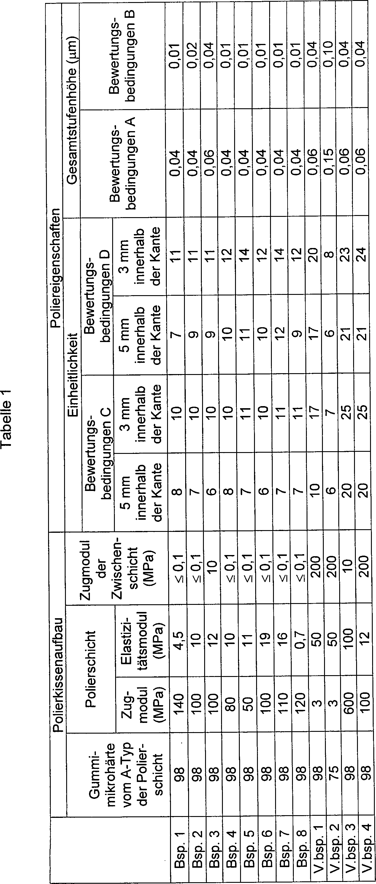
Claims (14)
Applications Claiming Priority (3)
| Application Number | Priority Date | Filing Date | Title |
|---|---|---|---|
| JP31767898 | 1998-11-09 | ||
| JP31767898 | 1998-11-09 | ||
| PCT/JP1999/006179 WO2000027589A1 (en) | 1998-11-09 | 1999-11-05 | Polishing pad and polishing device |
Publications (2)
| Publication Number | Publication Date |
|---|---|
| DE69932945D1 DE69932945D1 (en) | 2006-10-05 |
| DE69932945T2 true DE69932945T2 (en) | 2007-03-15 |
Family
ID=18090812
Family Applications (1)
| Application Number | Title | Priority Date | Filing Date |
|---|---|---|---|
| DE69932945T Expired - Lifetime DE69932945T2 (en) | 1998-11-09 | 1999-11-05 | POLISHING CUSHION AND POLISHING DEVICE |
Country Status (9)
| Country | Link |
|---|---|
| US (1) | US6362107B1 (en) |
| EP (1) | EP1138438B1 (en) |
| JP (1) | JP3685066B2 (en) |
| KR (1) | KR100628854B1 (en) |
| CN (1) | CN1099939C (en) |
| AT (1) | ATE337137T1 (en) |
| DE (1) | DE69932945T2 (en) |
| TW (1) | TW440947B (en) |
| WO (1) | WO2000027589A1 (en) |
Families Citing this family (39)
| Publication number | Priority date | Publication date | Assignee | Title |
|---|---|---|---|---|
| CN100496896C (en) * | 2000-12-01 | 2009-06-10 | 东洋橡膠工业株式会社 | Polishing pad |
| US6884507B2 (en) * | 2001-10-05 | 2005-04-26 | General Electric Company | Use of high modulus, impact resistant foams for structural components |
| US7025668B2 (en) * | 2002-06-18 | 2006-04-11 | Raytech Innovative Solutions, Llc | Gradient polishing pad made from paper-making fibers for use in chemical/mechanical planarization of wafers |
| AU2003292788A1 (en) * | 2002-12-26 | 2004-07-22 | Hoya Corporation | Glass substrate for information recording media and its fabricating method |
| JP2004303983A (en) * | 2003-03-31 | 2004-10-28 | Fuji Photo Film Co Ltd | Polishing pad |
| JP2005093785A (en) * | 2003-09-18 | 2005-04-07 | Toshiba Corp | Slurry for cmp, polish method, and method for manufacturing semiconductor device |
| US20050171224A1 (en) * | 2004-02-03 | 2005-08-04 | Kulp Mary J. | Polyurethane polishing pad |
| US7198549B2 (en) * | 2004-06-16 | 2007-04-03 | Cabot Microelectronics Corporation | Continuous contour polishing of a multi-material surface |
| US7189156B2 (en) * | 2004-08-25 | 2007-03-13 | Jh Rhodes Company, Inc. | Stacked polyurethane polishing pad and method of producing the same |
| US7275856B2 (en) * | 2004-09-30 | 2007-10-02 | Rohm And Haas Electronic Materials Cmp Holdings, Inc. | Apparatus for forming a polishing pad having a reduced striations |
| US7396497B2 (en) * | 2004-09-30 | 2008-07-08 | Rohm And Haas Electronic Materials Cmp Holdings, Inc. | Method of forming a polishing pad having reduced striations |
| US7275928B2 (en) * | 2004-11-23 | 2007-10-02 | Rohm And Haas Electronic Materials Cmp Holdings, Inc. | Apparatus for forming a striation reduced chemical mechanical polishing pad |
| US20060108701A1 (en) * | 2004-11-23 | 2006-05-25 | Saikin Allan H | Method for forming a striation reduced chemical mechanical polishing pad |
| TWI386989B (en) * | 2005-02-25 | 2013-02-21 | Ebara Corp | Polishing apparatus and polishing method |
| CN100580885C (en) * | 2006-02-06 | 2010-01-13 | 东丽株式会社 | Polishing pad, polishing apparatus, protection film for the polishing apparatus and polishing method |
| WO2008012909A1 (en) * | 2006-07-28 | 2008-01-31 | Toray Industries, Inc. | Interpenetrating polymer network structure and polishing pad and processes for producing them |
| US7371160B1 (en) | 2006-12-21 | 2008-05-13 | Rohm And Haas Electronic Materials Cmp Holdings Inc. | Elastomer-modified chemical mechanical polishing pad |
| US7438636B2 (en) * | 2006-12-21 | 2008-10-21 | Rohm And Haas Electronic Materials Cmp Holdings, Inc. | Chemical mechanical polishing pad |
| JP5292958B2 (en) * | 2007-07-18 | 2013-09-18 | 東レ株式会社 | Polishing pad |
| US20090094900A1 (en) * | 2007-10-15 | 2009-04-16 | Ppg Industries Ohio, Inc. | Method of forming a polyurea polyurethane elastomer containing chemical mechanical polishing pad |
| JP5233292B2 (en) * | 2008-01-23 | 2013-07-10 | 日立電線株式会社 | Cable type load sensor |
| US20110045753A1 (en) * | 2008-05-16 | 2011-02-24 | Toray Industries, Inc. | Polishing pad |
| US20100035529A1 (en) * | 2008-08-05 | 2010-02-11 | Mary Jo Kulp | Chemical mechanical polishing pad |
| US8303375B2 (en) | 2009-01-12 | 2012-11-06 | Novaplanar Technology, Inc. | Polishing pads for chemical mechanical planarization and/or other polishing methods |
| CN102029571B (en) * | 2009-09-24 | 2015-07-29 | 贝达先进材料股份有限公司 | Grinding pad and its application and its manufacture method |
| KR101435252B1 (en) * | 2012-03-30 | 2014-08-28 | 주식회사 엘지화학 | Pressure sensitive adhesive tape |
| TWI556910B (en) * | 2013-10-01 | 2016-11-11 | 三芳化學工業股份有限公司 | Composite polishing pad and method for making the same |
| US9216489B2 (en) * | 2014-03-28 | 2015-12-22 | Rohm And Haas Electronic Materials Cmp Holdings, Inc. | Chemical mechanical polishing pad with endpoint detection window |
| CN105881198A (en) * | 2014-12-29 | 2016-08-24 | 天津西美科技有限公司 | Adsorption gasket used for polishing template |
| CN104772661B (en) * | 2015-04-01 | 2017-12-12 | 中国科学院上海光学精密机械研究所 | The processing method of full frequency band High-precision aspheric optical element |
| CN104772668A (en) * | 2015-04-01 | 2015-07-15 | 中国科学院上海光学精密机械研究所 | Flexible self adaption polishing small tool for machining non-spherical surface |
| CN106046313A (en) * | 2016-06-03 | 2016-10-26 | 湖北鼎龙化学股份有限公司 | Chemical-mechanical polishing pad, buffer layer and preparation method of buffer layer |
| US20180134918A1 (en) * | 2016-11-11 | 2018-05-17 | Jh Rhodes Company, Inc. | Soft polymer-based material polishing media |
| JP6937117B2 (en) * | 2016-12-27 | 2021-09-22 | 東レコーテックス株式会社 | Abrasive pad |
| CN107053030A (en) * | 2017-01-06 | 2017-08-18 | 浙江工业大学 | A kind of fan-shaped combined type polishing disk with gradient function |
| CN109693176B (en) * | 2019-01-15 | 2020-12-08 | 湖北鼎汇微电子材料有限公司 | Polishing layer, polishing pad and preparation method |
| TWI761921B (en) * | 2019-10-30 | 2022-04-21 | 南韓商Skc索密思股份有限公司 | Polishing pad, process for preparing the same, and process for preparing a semiconductor device using the same |
| US20230211455A1 (en) * | 2020-06-25 | 2023-07-06 | 3M Innovative Properties Company | Polishing pads and systems for and methods of using same |
| CN112952094A (en) * | 2021-01-26 | 2021-06-11 | 宁德新能源科技有限公司 | Lithium ion battery and electronic device |
Family Cites Families (7)
| Publication number | Priority date | Publication date | Assignee | Title |
|---|---|---|---|---|
| US5257478A (en) * | 1990-03-22 | 1993-11-02 | Rodel, Inc. | Apparatus for interlayer planarization of semiconductor material |
| US5564965A (en) * | 1993-12-14 | 1996-10-15 | Shin-Etsu Handotai Co., Ltd. | Polishing member and wafer polishing apparatus |
| JPH08132342A (en) * | 1994-11-08 | 1996-05-28 | Hitachi Ltd | Manufacturing device for semiconductor integrated circuit device |
| JPH0950974A (en) * | 1995-08-07 | 1997-02-18 | Sony Corp | Polishing cloth and manufacture of semiconductor device |
| JP3239764B2 (en) * | 1996-07-17 | 2001-12-17 | 株式会社ニコン | Polishing apparatus and polishing polisher for CMP |
| JPH10156724A (en) * | 1996-11-28 | 1998-06-16 | Sony Corp | Abrasive cloth, flattening polishing method using this abrasive cloth, and manufacture of semiconductor device |
| US6022268A (en) * | 1998-04-03 | 2000-02-08 | Rodel Holdings Inc. | Polishing pads and methods relating thereto |
-
1999
- 1999-11-05 JP JP2000580803A patent/JP3685066B2/en not_active Expired - Fee Related
- 1999-11-05 AT AT99954409T patent/ATE337137T1/en not_active IP Right Cessation
- 1999-11-05 KR KR1020017005781A patent/KR100628854B1/en not_active IP Right Cessation
- 1999-11-05 CN CN99814332A patent/CN1099939C/en not_active Expired - Fee Related
- 1999-11-05 DE DE69932945T patent/DE69932945T2/en not_active Expired - Lifetime
- 1999-11-05 WO PCT/JP1999/006179 patent/WO2000027589A1/en active IP Right Grant
- 1999-11-05 US US09/831,292 patent/US6362107B1/en not_active Expired - Lifetime
- 1999-11-05 EP EP99954409A patent/EP1138438B1/en not_active Expired - Lifetime
- 1999-11-08 TW TW088119478A patent/TW440947B/en not_active IP Right Cessation
Also Published As
| Publication number | Publication date |
|---|---|
| US6362107B1 (en) | 2002-03-26 |
| CN1099939C (en) | 2003-01-29 |
| DE69932945D1 (en) | 2006-10-05 |
| WO2000027589A1 (en) | 2000-05-18 |
| JP3685066B2 (en) | 2005-08-17 |
| EP1138438A1 (en) | 2001-10-04 |
| TW440947B (en) | 2001-06-16 |
| CN1330581A (en) | 2002-01-09 |
| ATE337137T1 (en) | 2006-09-15 |
| KR20010099795A (en) | 2001-11-09 |
| KR100628854B1 (en) | 2006-09-27 |
| EP1138438B1 (en) | 2006-08-23 |
| EP1138438A4 (en) | 2002-08-07 |
Similar Documents
| Publication | Publication Date | Title |
|---|---|---|
| DE69932945T2 (en) | POLISHING CUSHION AND POLISHING DEVICE | |
| DE69937355T2 (en) | POLISHING CUSHION | |
| DE602004000805T2 (en) | Polishing pad with a window of high optical transmission | |
| DE60109601T2 (en) | RILLEN POLISHING PILLOWS FOR CHEMICAL-MECHANICAL PLANARIZATION | |
| DE112006001927B4 (en) | Polishing pad containing a interstitial network of liquefied vinyl monomer with polyurethane matrix therein | |
| DE102014012353A1 (en) | CHEMICAL MECHANICAL POLISH PILLOW | |
| DE102014012378A1 (en) | PROCESS FOR CHEMICAL-MECHANICAL POLISHING OF A SUBSTRATE | |
| US20070010175A1 (en) | Polishing pad and method of producing same | |
| DE102012018523A1 (en) | Chemically-mechanical acrylate polyurethane polishing layer | |
| DE102014007027A1 (en) | Soft and conditionable chemical-mechanical window polishing pad | |
| DE102015003240A1 (en) | CHEMICAL-MECHANICAL POLISHING CUSHION WITH POLISHING LAYER AND WINDOW | |
| DE102015003200A1 (en) | SOFT AND CONDENSABLE CHEMICAL MECHANICAL POLISHING CUSHION WITH WINDOW | |
| DE102019007230A1 (en) | CHEMICAL-MECHANICAL POLISHING CUSHION AND POLISHING METHOD | |
| DE102016012533A1 (en) | Chemical-mechanical polishing process | |
| JP2007521980A (en) | Polishing pad base pad and multilayer pad including the same | |
| CN113442056A (en) | Polishing pad, preparation method thereof and manufacturing method of semiconductor device | |
| JP4686912B2 (en) | Polishing pad | |
| JP3924952B2 (en) | Polishing apparatus and polishing pad | |
| DE102022122010A1 (en) | COMPRESSABLE NON-NETWORK POLYUREA POLISHING PAD | |
| DE102015000701A1 (en) | Improved process for the production of chemical-mechanical polishing layers | |
| DE102022114532A1 (en) | CMP POLISHING PAD | |
| WO2022210264A1 (en) | Polishing pad and method for manufacturing polished workpiece | |
| JP2000071167A (en) | Abrasive pad | |
| JP4701066B2 (en) | Polyurethane foam and method for producing the same | |
| US20230364736A1 (en) | Polishing pad |
Legal Events
| Date | Code | Title | Description |
|---|---|---|---|
| 8364 | No opposition during term of opposition |