CN108594599B - Resist material, lithographic patterning method and use of oxides - Google Patents
Resist material, lithographic patterning method and use of oxides Download PDFInfo
- Publication number
- CN108594599B CN108594599B CN201810445598.3A CN201810445598A CN108594599B CN 108594599 B CN108594599 B CN 108594599B CN 201810445598 A CN201810445598 A CN 201810445598A CN 108594599 B CN108594599 B CN 108594599B
- Authority
- CN
- China
- Prior art keywords
- resist material
- resist
- euv
- radiation
- substrate
- Prior art date
- Legal status (The legal status is an assumption and is not a legal conclusion. Google has not performed a legal analysis and makes no representation as to the accuracy of the status listed.)
- Active
Links
Images


Classifications
-
- G—PHYSICS
- G03—PHOTOGRAPHY; CINEMATOGRAPHY; ANALOGOUS TECHNIQUES USING WAVES OTHER THAN OPTICAL WAVES; ELECTROGRAPHY; HOLOGRAPHY
- G03F—PHOTOMECHANICAL PRODUCTION OF TEXTURED OR PATTERNED SURFACES, e.g. FOR PRINTING, FOR PROCESSING OF SEMICONDUCTOR DEVICES; MATERIALS THEREFOR; ORIGINALS THEREFOR; APPARATUS SPECIALLY ADAPTED THEREFOR
- G03F7/00—Photomechanical, e.g. photolithographic, production of textured or patterned surfaces, e.g. printing surfaces; Materials therefor, e.g. comprising photoresists; Apparatus specially adapted therefor
- G03F7/004—Photosensitive materials
- G03F7/038—Macromolecular compounds which are rendered insoluble or differentially wettable
- G03F7/0388—Macromolecular compounds which are rendered insoluble or differentially wettable with ethylenic or acetylenic bands in the side chains of the photopolymer
-
- G—PHYSICS
- G03—PHOTOGRAPHY; CINEMATOGRAPHY; ANALOGOUS TECHNIQUES USING WAVES OTHER THAN OPTICAL WAVES; ELECTROGRAPHY; HOLOGRAPHY
- G03F—PHOTOMECHANICAL PRODUCTION OF TEXTURED OR PATTERNED SURFACES, e.g. FOR PRINTING, FOR PROCESSING OF SEMICONDUCTOR DEVICES; MATERIALS THEREFOR; ORIGINALS THEREFOR; APPARATUS SPECIALLY ADAPTED THEREFOR
- G03F7/00—Photomechanical, e.g. photolithographic, production of textured or patterned surfaces, e.g. printing surfaces; Materials therefor, e.g. comprising photoresists; Apparatus specially adapted therefor
- G03F7/004—Photosensitive materials
- G03F7/0042—Photosensitive materials with inorganic or organometallic light-sensitive compounds not otherwise provided for, e.g. inorganic resists
-
- C—CHEMISTRY; METALLURGY
- C08—ORGANIC MACROMOLECULAR COMPOUNDS; THEIR PREPARATION OR CHEMICAL WORKING-UP; COMPOSITIONS BASED THEREON
- C08F—MACROMOLECULAR COMPOUNDS OBTAINED BY REACTIONS ONLY INVOLVING CARBON-TO-CARBON UNSATURATED BONDS
- C08F30/00—Homopolymers and copolymers of compounds having one or more unsaturated aliphatic radicals, each having only one carbon-to-carbon double bond, and containing phosphorus, selenium, tellurium or a metal
- C08F30/04—Homopolymers and copolymers of compounds having one or more unsaturated aliphatic radicals, each having only one carbon-to-carbon double bond, and containing phosphorus, selenium, tellurium or a metal containing a metal
- C08F30/08—Homopolymers and copolymers of compounds having one or more unsaturated aliphatic radicals, each having only one carbon-to-carbon double bond, and containing phosphorus, selenium, tellurium or a metal containing a metal containing silicon
-
- G—PHYSICS
- G03—PHOTOGRAPHY; CINEMATOGRAPHY; ANALOGOUS TECHNIQUES USING WAVES OTHER THAN OPTICAL WAVES; ELECTROGRAPHY; HOLOGRAPHY
- G03F—PHOTOMECHANICAL PRODUCTION OF TEXTURED OR PATTERNED SURFACES, e.g. FOR PRINTING, FOR PROCESSING OF SEMICONDUCTOR DEVICES; MATERIALS THEREFOR; ORIGINALS THEREFOR; APPARATUS SPECIALLY ADAPTED THEREFOR
- G03F7/00—Photomechanical, e.g. photolithographic, production of textured or patterned surfaces, e.g. printing surfaces; Materials therefor, e.g. comprising photoresists; Apparatus specially adapted therefor
- G03F7/004—Photosensitive materials
- G03F7/0042—Photosensitive materials with inorganic or organometallic light-sensitive compounds not otherwise provided for, e.g. inorganic resists
- G03F7/0043—Chalcogenides; Silicon, germanium, arsenic or derivatives thereof; Metals, oxides or alloys thereof
-
- G—PHYSICS
- G03—PHOTOGRAPHY; CINEMATOGRAPHY; ANALOGOUS TECHNIQUES USING WAVES OTHER THAN OPTICAL WAVES; ELECTROGRAPHY; HOLOGRAPHY
- G03F—PHOTOMECHANICAL PRODUCTION OF TEXTURED OR PATTERNED SURFACES, e.g. FOR PRINTING, FOR PROCESSING OF SEMICONDUCTOR DEVICES; MATERIALS THEREFOR; ORIGINALS THEREFOR; APPARATUS SPECIALLY ADAPTED THEREFOR
- G03F7/00—Photomechanical, e.g. photolithographic, production of textured or patterned surfaces, e.g. printing surfaces; Materials therefor, e.g. comprising photoresists; Apparatus specially adapted therefor
- G03F7/004—Photosensitive materials
- G03F7/075—Silicon-containing compounds
- G03F7/0757—Macromolecular compounds containing Si-O, Si-C or Si-N bonds
- G03F7/0758—Macromolecular compounds containing Si-O, Si-C or Si-N bonds with silicon- containing groups in the side chains
-
- G—PHYSICS
- G03—PHOTOGRAPHY; CINEMATOGRAPHY; ANALOGOUS TECHNIQUES USING WAVES OTHER THAN OPTICAL WAVES; ELECTROGRAPHY; HOLOGRAPHY
- G03F—PHOTOMECHANICAL PRODUCTION OF TEXTURED OR PATTERNED SURFACES, e.g. FOR PRINTING, FOR PROCESSING OF SEMICONDUCTOR DEVICES; MATERIALS THEREFOR; ORIGINALS THEREFOR; APPARATUS SPECIALLY ADAPTED THEREFOR
- G03F7/00—Photomechanical, e.g. photolithographic, production of textured or patterned surfaces, e.g. printing surfaces; Materials therefor, e.g. comprising photoresists; Apparatus specially adapted therefor
- G03F7/20—Exposure; Apparatus therefor
- G03F7/2002—Exposure; Apparatus therefor with visible light or UV light, through an original having an opaque pattern on a transparent support, e.g. film printing, projection printing; by reflection of visible or UV light from an original such as a printed image
Landscapes
- Physics & Mathematics (AREA)
- General Physics & Mathematics (AREA)
- Chemical & Material Sciences (AREA)
- Organic Chemistry (AREA)
- Spectroscopy & Molecular Physics (AREA)
- Metallurgy (AREA)
- Engineering & Computer Science (AREA)
- Health & Medical Sciences (AREA)
- Chemical Kinetics & Catalysis (AREA)
- Medicinal Chemistry (AREA)
- Polymers & Plastics (AREA)
- Exposure And Positioning Against Photoresist Photosensitive Materials (AREA)
- Exposure Of Semiconductors, Excluding Electron Or Ion Beam Exposure (AREA)
- Materials For Photolithography (AREA)
- Addition Polymer Or Copolymer, Post-Treatments, Or Chemical Modifications (AREA)
Abstract
A resist material, a lithographic patterning method and use of an oxide, the resist material comprising an oxide comprising at least one element selected from the group consisting of: ta, Re, Os, Ir, Ni, Cu, and Zn, wherein the resist material is sensitive to EUV light having a wavelength of less than 11 nm.
Description
The present application is a divisional application of chinese patent application having application number "201280033742.3" entitled "lithographic patterning process and resist used therein", filed on 30/5/2012.
Cross Reference to Related Applications
This application claims the benefit of U.S. provisional application 61/505, 768 filed 7/8/2011, which is hereby incorporated by reference in its entirety.
Technical Field
The present invention relates to the use of particular silicon-containing polymers or compounds comprising specific metals for lithographic purposes and novel patterning methods or processes using such polymers or compounds. The invention also relates to the silicon-containing polymer itself and to the use of a silicon-containing polymer or compound comprising a specific metal as a resist in a lithographic process involving Extreme Ultraviolet (EUV) radiation emitting at a wavelength of less than 11 nm.
Background
In lithography, a desired pattern is applied to a substrate, usually to a target portion of the substrate. Lithographic apparatus can be used, for example, in the manufacture of Integrated Circuits (ICs). In such cases, a patterning device, which is alternatively referred to as a mask or a reticle, may be used to generate a circuit pattern to be formed on an individual layer of the IC. Such a pattern can be transferred onto a target portion on a substrate, such as a silicon wafer. Typically, pattern transfer is by imaging a pattern onto a layer of radiation-sensitive material, commonly referred to as resist, disposed on a substrate. Typically, a single substrate will contain a network of adjacent target portions that are successively patterned.
Photolithography is widely recognized as one of the key steps in the manufacture of ICs and other devices and/or structures. However, as the dimensions of features fabricated using photolithography become smaller and smaller, photolithography is becoming a more critical factor allowing the fabrication of miniature ICs or other devices and/or structures. The theoretical estimate of the limit of pattern printing can be given by the rayleigh law for resolution as shown in equation (1):

where λ is the wavelength of the radiation used, NA is the numerical aperture of the projection system used to print the pattern, k1Is a process dependent adjustment factor, also known as the rayleigh constant, and the CD is the feature size (or critical dimension) of the printed feature. It is known from equation (1) that reducing the minimum printable size of a feature can be achieved in three ways: by shortening the exposure wavelength λ, by increasing the numerical aperture NA or by decreasing k1The value of (c).
In order to shorten the exposure wavelength, and thus reduce the minimum printable size, it has been proposed to use an Extreme Ultraviolet (EUV) radiation source. The EUV radiation has a wavelength in the range of 5-20nm, for example in the range of 13-14 nm. This radiation is sometimes referred to as soft X-rays. EUV radiation may be generated by using a plasma. A radiation system for producing EUV radiation may include a laser for exciting a fuel to provide a plasma and a source collector module for containing the plasma. The plasma may be generated, for example, by directing a laser beam at a fuel such as particles of a suitable material (e.g., tin) or a stream of a suitable gas or vapor (e.g., xenon or lithium vapor). Such radiation systems are commonly referred to as Laser Produced Plasma (LPP) sources. Alternative sources include discharge plasma sources, or sources based on synchrotron radiation provided through an electron storage ring.
In EUV lithography, the choice of wavelength may be limited by practical considerations including the availability of suitable radiation sources, optical components, and process materials. Current EUV lithography systems all operate with radiation having a wavelength in the range of 13-14nm, and various developments are ongoing before EUV lithography is used in volume production. It is also proposed that EUV radiation with a wavelength of less than 11nm can be used, for example in the range of 5-10nm or in the range of 5-8nm, and in particular in the so-called '6. x' wavelength region of 6.5-6.9nm, for example 6.7nm or 6.8 nm. The invention resides in that shorter wavelengths can provide higher resolution (below 11nm node features), greater depth of focus (DOF) and higher productivity than the currently used 13.5nm radiation. However, the change in wavelength brings a new range for practical considerations, and techniques and materials optimized for 13.5nm may or may not work at shorter wavelengths.
A particular challenge in the development of commercial EUV lithography is the formulation of radiation sensitive resist materials that will achieve high resolution patterns projected by the EUV optics in the etch resist material. Some work that has been published has been directed to the development of resist materials that can be used at 13.5 nm. The present inventors have realised that very different solutions may be suitable for use at shorter wavelengths below 11 nm.
Disclosure of Invention
According to an aspect of the present invention, there is provided (i) a silicon-containing polymer or (ii) a compound including at least one element selected from the group consisting of: use of Ta, W, Re, Os, Ir, Ni, Cu and Zn in a resist material for EUV lithographic processes, wherein the EUV radiation wavelength used in the process is less than 11 nm. The wavelength is in the range of 5-8nm, such as in the range of 6.5-6.9nm, such as about 6.7nm or 6.8 nm.
In one embodiment, the resist material is deposited on the substrate as a film, and the film has a thickness in the range of 10nm to 100nm, for example less than 50nm or even less than 30 nm. In this way, the ratio of resist height to feature width can be kept less than 3, less than 2.5, or less than 2.
According to an aspect of the invention, there is provided a lithographic patterning process comprising: forming a film of a resist material on a substrate by using the material as described above; irradiating the resist film with a patterned beam of EUV radiation having a wavelength of less than 11 nm; and developing the resist film.
According to an aspect of the invention, there is provided a method of manufacturing a device in which patterned device features are applied to a substrate by a series of lithographic steps, at least one of which is a lithographic patterning process according to an aspect of the invention as described above, and other processing steps, the lithographic patterning process comprising the use of a material as a resist.
According to an aspect of the invention, there is provided a method of irradiating a resist film of a resist material with a patterned beam of EUV radiation having a wavelength of less than 11nm, the resist material comprising a silicon-containing polymer and a compound comprising at least one element selected from the following elements: ta, W, Re, Os, Ir, Ni, Cu and Zn.
According to an aspect of the present invention, there is provided a silicon-containing polymer comprising a monomer having the formula:

wherein R is C1To C20Alkylsilyl or a group of the formula:

wherein R is1、R2And R3Each is C1To C20An alkylsilyl group.
Silicon-containing polymers may be used as resists in lithographic processes. Specific examples and variations thereof are described further below to assist in understanding the invention.
Drawings
Embodiments of the invention will now be described, by way of example only, with reference to the accompanying schematic drawings in which:
FIG. 1 schematically depicts functional elements of a lithographic apparatus used in an embodiment of the invention;
FIG. 2 is a more detailed view of the apparatus of FIG. 1;
FIG. 3 shows different steps of a patterning process using a resist according to one embodiment of the invention;
FIG. 4 shows EUV emission curves of various silicon-containing polymers of embodiments of the present invention in comparison to known resists; and
figure 5 shows the emission curves of the monomeric units of the polymers of one embodiment of the invention at 6.5nm and 13.5nm, depending on the number of silicon atoms they contain, if any.
Detailed Description
FIG. 1 schematically depicts a lithographic apparatus 100 in an embodiment of a device manufacturing process according to an embodiment of the invention. The apparatus comprises: a source collector module SO; an illumination system (illuminator) IL configured to condition a radiation beam B (e.g. EUV radiation); a support structure (e.g. a mask table) MT constructed to support a patterning device (e.g. a mask or reticle) MA and connected to a first positioner PM configured to accurately position the patterning device; a substrate table (e.g. a wafer table) WT constructed to hold a substrate (e.g. a resist-coated wafer) W and connected to a second positioner PW configured to accurately position the substrate; and a projection system (e.g. a reflective projection system) PS configured to project a pattern imparted to the radiation beam B by patterning device MA onto a target portion C (e.g. comprising one or more dies) of the substrate W.
The illumination system may include various types of optical components, such as refractive, reflective, magnetic, electromagnetic, electrostatic or other types of optical components, or any combination thereof, for directing, shaping, or controlling radiation.
The support structure MT holds the patterning device MA in a manner that depends on the orientation of the patterning device, the design of the lithographic apparatus, and other conditions, such as for example whether or not the patterning device is held in a vacuum environment. The support structure may use mechanical, vacuum, electrostatic or other clamping techniques to hold the patterning device. The support structure may be a frame or a table, for example, which may be fixed or movable as required. The support structure may ensure that the patterning device is at a desired position, for example with respect to the projection system.
The term "patterning device" used herein should be broadly interpreted as referring to any device that can be used to impart a radiation beam with a pattern in its cross-section such as to create a pattern in a target portion of the substrate. The pattern imparted to the radiation beam may correspond to a particular functional layer in a device being created in the target portion, such as an integrated circuit.
The patterning device may be transmissive or reflective. Examples of patterning devices include masks, programmable mirror arrays, and programmable Liquid Crystal Display (LCD) panels. Masks are well known in lithography, and include mask types such as binary, alternating phase-shift, attenuated phase-shift, and various hybrid mask types. An example of a programmable mirror array employs a matrix arrangement of small mirrors, each of which can be individually tilted so as to reflect an incoming radiation beam in different directions. The tilted mirrors impart a pattern in a radiation beam which is reflected by the mirror matrix.
The projection system, like the illumination system, may include various types of optical components, such as refractive, reflective, magnetic, electromagnetic and electrostatic or other types of optical components, or any combination thereof, as appropriate for the exposure radiation being used, or for other factors such as the use of an immersion liquid or the use of a vacuum. It may be desirable to use a vacuum for EUV radiation because other gases may absorb too much radiation. Thus providing a vacuum environment for the entire beam path by means of the vacuum wall and the vacuum pump.
As here depicted, the apparatus is of a reflective type (e.g. employing a reflective mask).
The lithographic apparatus may be of a type having two (dual stage) or more substrate tables (and/or two or more mask tables). In such "multiple stage" machines the additional tables may be used in parallel, or preparatory steps may be carried out on one or more tables while one or more other tables are being used for exposure.
Referring to FIG. 1, the illuminator IL receives an EUV radiation beam from a source collector module SO. Methods to produce EUV light include, but are not necessarily limited to, converting a material into a plasma state having at least one element, such as xenon, lithium, or tin, with one or more emission lines in the EUV range. In one such method, commonly referred to as laser produced plasma ("LPP"), a desired plasma can be generated by irradiating a fuel, such as a droplet, stream or cluster of material having a desired emission line element, with a laser beam. The source collector module SO may be part of an EUV radiation system comprising a laser (not shown in fig. 1) for providing a laser beam to excite the fuel. The resulting plasma emits output radiation, e.g., EUV radiation, which is collected using a radiation collector disposed in the source collector module. The laser and the source collector module may be separate entities, for example when using CO2The laser provides a laser beam for fuel excitation.
In such cases, the laser is not considered to form part of the lithographic apparatus and the radiation beam is passed from the laser to the source collector module by means of a beam delivery system comprising, for example, suitable directing mirrors and/or a beam expander. In other cases, the source may be an integral part of the source collector module, for example when the source is a discharge produced plasma EUV generator (commonly referred to as a DPP source).
The illuminator IL may comprise an adjuster configured to adjust the angular intensity distribution of the radiation beam. Generally, at least the outer and/or inner radial extent (commonly referred to as σ -outer and σ -inner, respectively) of the intensity distribution in a pupil plane of the illuminator can be adjusted. In addition, the illuminator IL may include various other components, such as a faceted field mirror device and a faceted pupil mirror device (which may also be referred to as a multi-faceted field mirror device and a multi-faceted pupil mirror device). The illuminator may be used to condition the radiation beam, to have a desired uniformity and intensity distribution in its cross-section.
The radiation beam B is incident on the patterning device (e.g., mask) MA, which is held on the support structure (e.g., mask table) MT, and is patterned by the patterning device. Having been reflected by the patterning device (e.g. mask) MA, the radiation beam B passes through the projection system PS, which focuses the beam onto a target portion C of the substrate W. With the aid of the second positioner PW and position sensor PS2 (e.g. an interferometric device, linear encoder or capacitive sensor), the substrate table WT can be moved accurately, e.g. so as to position different target portions C in the path of the radiation beam B. Similarly, the first positioner PM and another position sensor PS1 can be used to accurately position the patterning device (e.g. mask) MA with respect to the path of the radiation beam B. Patterning device (e.g. mask) MA and substrate W may be aligned using mask alignment marks M1, M2 and substrate alignment marks P1, P2.
The device may be used in at least one of the following modes:
1. in step mode, the support structure (e.g. mask table) MT and the substrate table WT are kept essentially stationary, while an entire pattern imparted to the radiation beam is projected onto a target portion C at one time (i.e. a single static exposure). The substrate table WT is then shifted in the X and/or Y direction so that a different target portion C can be exposed.
2. In scan mode, the support structure (e.g. mask table) MT and the substrate table WT are scanned synchronously while a pattern imparted to the radiation beam is projected onto a target portion C (i.e. a single dynamic exposure). The velocity and direction of the substrate table WT relative to the support structure (e.g. mask table) MT may be determined by the (de-) magnification and image reversal characteristics of the projection system PS.
3. In another mode, a support structure (e.g. a mask table) MT is kept essentially stationary holding a programmable patterning device, and a pattern imparted to the radiation beam is projected onto a target portion C while the substrate table WT is moved or scanned. In this mode, generally a pulsed radiation source is employed and the programmable patterning device is updated as required after each movement of the substrate table WT or in between successive radiation pulses during a scan. This mode of operation can be readily applied to maskless lithography that utilizes programmable patterning device, such as a programmable mirror array of a type as referred to above.
Combinations and/or variations on the above described modes of use or entirely different modes of use may also be employed.
Fig. 2 shows the apparatus 100 in more detail, comprising the source collector module SO, the illumination system IL and the projection system PS. The source collector module SO is constructed and arranged such that a vacuum environment is maintained within the enclosure 220 of the source collector module SO. The plasma source produced by the discharge forms a plasma 210 for emitting EUV radiation. EUV radiation may be formed from a gas or vapor, such as xenon, lithium vapor, or tin vapor, in which a very high temperature plasma 210 is generated to emit radiation in the EUV range of the electromagnetic spectrum. The very high temperature plasma 210 is generated by causing an at least partially ionized plasma, for example, by an electrical discharge. For efficient generation of radiation, xenon, lithium, tin vapour or any other suitable gas or vapour may be required, for example at a partial pressure of 10 Pa. In one embodiment, an energized tin (Sn) plasma is provided to generate EUV radiation.
Radiation emitted by the high temperature plasma 210 passes from the source cavity 211 into the collector cavity 212 via an optional gas barrier or contaminant trap 230 (also referred to as a contaminant barrier or foil trap in some cases) positioned within or behind an opening in the source cavity 211. Contaminant trap 230 may include a channel structure. Contaminant trap 230 may also include a gas barrier or a combination of a gas barrier and a channel structure. The contaminant trap or contaminant barrier 230 shown here also includes at least a channel structure, as will be appreciated by those skilled in the art.
The collector chamber 211 may comprise a radiation collector CO, which may be a so-called grazing incidence collector. The radiation collector CO has an upstream radiation collector side 251 and a downstream radiation collector side 252. Radiation passing through the collector CO may be reflected off the grating spectral filter 240 to be focused at the virtual source point IF. The virtual source point IF is commonly referred to as the intermediate focus, and the source collector module is arranged such that the intermediate focus IF is located at or near the opening 221 in the enclosing structure 220. The virtual source point IF is an image of the plasma 210 for emitting radiation.
The radiation then passes through an illumination system IL, which may comprise a faceted pupil mirror device 24 and a faceted field mirror device 22 arranged to provide a desired angular distribution of the radiation beam 21 at patterning device MA, and a desired uniformity of radiation intensity at patterning device MA. After the radiation beam 21 is reflected at the patterning device MA, which is held by the support structure MT, a patterned beam 26 is formed and the patterned beam 26 is imaged by the projection system PS via reflective elements 28, 30 onto a substrate W held by the wafer or substrate table WT.
There are typically more elements in the illumination optics IL and projection system PS than shown. The grating spectral filter 240 may be optional, depending on the type of lithographic apparatus. Furthermore, there may be more mirrors than those shown in the figures, e.g. 1-6 additional reflective elements may be present within the projection system PS than those shown in fig. 2.
As shown in fig. 2, collector optic CO is illustrated as a nested collector with grazing incidence reflectors 253, 254, and 255, as just one example of a collector (or collector mirror). Grazing incidence reflectors 253, 254 and 255 are arranged axially symmetrically about optical axis O and collector devices CO of this type are preferably used in combination with a discharge produced plasma source, commonly referred to as a DPP source.
Alternatively, the source collector module SO may be part of an LPP radiation system using near normal incidence collector optics (not shown). In LPP systems, a laser is arranged to deposit laser energy onto the fuel material, thereby producing a highly ionized plasma with an electron temperature of a few tens of electron volts. Energetic radiation generated during de-excitation and re-recombination of these ions is emitted from the plasma through a near normal incidence collector opticThe device CO collects and focuses onto the opening 221 in the enclosing structure 220. For the wavelength of 13.5nm, for example, xenon (Xe), tin (Sn), lithium (Li), or other fuels are used. Gd and Tb and their alloys and compounds (e.g. Gd) for 6, xnm wavelengths2O3) Are candidates. The energy of each photon may be greater than 100eV, for example about 188 eV.
Device manufacturing process
A typical patterning process, which is part of a method of manufacturing a device, typically uses an apparatus such as that of figures 1 and 2 to transfer a pattern from the patterning device M to a radiation-sensitive resist material (simply "resist") on the substrate W.
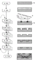
Fig. 3 shows seven steps (S0 to S7) involved in a patterning process using a resist for manufacturing an object such as an integrated circuit. These steps are as follows:
s0: a substrate W, which may be, for example, a silicon wafer, is prepared.
S1 (coating): the resist solution is spin-coated on the substrate W to form an extremely thin uniform layer. The resist layer may be baked at low temperature to evaporate residual solvent.
S2 (exposure): a latent image is formed on the resist layer by exposure to EUV using lithographic apparatus 100 and a suitable patterning device M.
S3 (development and etching): in the case of a "positive" resist, the areas of resist that have been exposed to light are removed by rinsing with a suitable solvent. In the case of a "negative" resist, the unexposed areas are removed. This step is combined with or followed by a processing step of the resist pattern of the substrate. The term "etching" is used in the drawings as an example only. The processing steps may include wet or dry etching, stripping, doping, etc. Regardless of the process or technology by which the applied pattern is embedded during the addition, removal, or modification of material on the substrate. The removal of material is shown in preparation for deposition step S5.
S4 (peeling): the remaining resist is removed from the patterned substrate W.
S5 (deposition): different substances are deposited to fill the pattern of the substrate W.
S6 (polishing): excess material is removed from the surface of the wafer W by polishing, leaving only the desired pattern within the wafer W.
The steps S1 to S6 are repeated in different patterns and different processing steps to form functional features having desired patterns in different layers above or below the original surface of the substrate W until the final multilayer product is achieved (step S7). The product generally need not be a semiconductor device, such as an integrated circuit.
As described above, the skilled reader will recognize that steps S4 to S6 are only one example of a process that may be applied in a pattern determined by an exposed resist. Many different types of steps can be used and will be used at different stages of production. For example, the resist may be used to control modification of the underlying material rather than etching it away. The modification may be, for example, oxidation, doping, for example by diffusion or ion implantation. A new layer of material may be deposited on top of the substrate. In many processes, the photoresist is only an intermediate stage in the fabrication of a so-called "hard mask" that reproduces the exposed pattern in a different material. The hard mask is then used to control the process steps of etching or modifying the underlying material in the desired pattern but will not be controlled by the photoresist itself. Thus, depending on the sought order of the pattern and layers formed and the intermediate steps required to form the final device, the above-described process may vary: certain steps are combined and/or eliminated, as well as certain additional steps.
When considering a resist suitable for use in an EUV lithography process below 11nm given by the 6.x nm wavelength example, the inventors have realised that a number of issues are to be considered.
When considering the 6.x technique in EUV lithography, the aspect ratio (height to width ratio) of the features to be obtained in the resist should be at most 3, desirably 2, and thus the thickness of the resist film considered is reduced to the range of about 10nm to about 100 nm. This is because of the reduction in the depth of focus of the image projected on the resist. Thus, a thinner resist film is desirable. However, the protective action of the resist and in particular its resistance to etching may not be achieved with thinner films, for example, due to thickness variations and microchannel configuration. Thinner films can result in increased thickness variation across the film. This in turn may adversely affect subsequent layers of material provided on the semiconductor device. Further, the microchannel configuration in the thinner film may reach the substrate and expose the substrate to an etching process. This will result in the resist not meeting minimum performance requirements.
EUV radiation is absorbed by the resist material and photoelectrons and secondary electrons are generated. The secondary electrons cause some random exposure which is superimposed on the optical image applied on the resist by the EUV source. This in turn leads to loss of resolution, observable line edge roughness, and line width variation, which are known as the "blurring" phenomenon. This blur will need to be controlled if the resist is to deliver the high resolution desired in EUV lithography.
Pattern collapse occurs when the physical properties of the resist material are unable to counteract the repulsive or capillary forces applied to the pattern during drying of the rinsing liquid to a sufficient extent. A high stiffness or strength of the resist material is therefore desirable, as well as a reduced aspect ratio of the features of the pattern.
Other process parameters that lead to variations in the resolving power of the resist are, for example, etch resistance and selectivity, quantum yield (quantum yield), bake time and temperature, exposure time and source output, aerial image focus and development time and temperature. The ability of a particular resist to allow some degree of variation in these particular parameters is of course highly desirable to be able to operate within specific tolerances.
EUV resist-background knowledge
Organic resist
Conventional organic resists are based on polyhydroxystyrene (polyhydroxystyrene), such as PBS, poly (butene-1-sulfone), and ZEP, poly (methyl a-chloroacrylate-co-a-methylstyrene). These polystyrene hydride based resins are suitable for patterns larger than 180 nm. Chemically Amplified Resist (CAR) resins were developed as part of the history of changes from 365nm (i-line) to 248nm (KrF). These resins are also used in conjunction with 193nm (arf) dry and immersion lithography. Although not designed for EUV, their good performance has led to their use in 13-14nm technology because of their high sensitivity and contrast, high resolution, dry etch resistance, aqueous development (aqueous development), and process latitude.
In this process, a portion of the chemical components present on the resin release acid radicals upon exposure to radiation. These acid groups diffuse during the post-exposure bake step and cause the surrounding polymer to dissolve in the developer. Acid diffusion helps to increase the sensitivity and productivity of the resist and also helps to limit line edge roughness due to shot noise (shot noise) statistics. However, the acid diffusion length itself is a potential limiting factor. Furthermore, too much diffusion may reduce chemical contrast, which in turn may lead to greater roughness. KRS-XE is a CAR developed by IBM and has high contrast and is based on the use of acetal protecting groups that avoid the need for post-exposure baking.
U.S. patent application publication No. 2004/0241574, describes a CAR that contains silicon or boron. These CARs are described as very suitable resists due to the high transparency compared to pure carbon-based polymers under the selection of EUV wavelengths, which are disclosed in us patent application publication No. 2004/0241574 as being above 12.5 nm. The present inventors have realised that for lithographic processes using EUV below 11nm, high transparency characteristics are undesirable, which indicate a lack of interaction between material and radiation, and that it is desirable to use much thinner resist films with low haze, as described above.
Inorganic resist
The resist may also be formed of inorganic materials, such as various metal oxides. The inorganic resist may exhibit enhanced resistance to blurring and enhanced resistance to pattern collapse due to its strength. Stowers et al, in proceedings of the SPIE, Volume 7969, pp 796915-796915-11 (2011) describe the use of hafnium oxide sulfate in combination with a peroxy complexing agent to form a negative resist. Exposure to EUV results in the generation of secondary electrons which break down the peroxide-based bonds. Reactive metal sites are thus formed, which react to form cross-linked and concentrated regions. The unexposed regions are removed by using a solvent such as TMAH (tetramethylammonium hydroxide).
Resist washout for sub-11 nm EUV lithography
It is therefore highly desirable to provide a resist material which can meet the requirements of EUV lithography using wavelengths of less than 11nm, and in particular 6. xnm. It has now been found that (i) silicon-containing organic polymers and (ii) thin resist films comprising Ta, W, Re, Os, Ir, Ni, Cu or Zn or mixtures thereof can be particularly advantageous and provide high absorption and less haze due to a reduction in the mean free path of the photogenerated electrons. Thus, the mean free path of resist materials according to the invention is about 2nm, whereas the mean free path of currently used resist materials is about 7 nm.
Example 1: silicon-containing polymers
According to one embodiment of the present invention, a suitable silicon-containing polymer may include from about 0.1 wt% to about 50 wt% silicon. Such polymers can be obtained, for example, by replacing a portion of the alkyl groups of known CARs with silyl groups. Suitable known CARs may include any known polymeric resist material used with EUV lithography processes, such as KRS or polyhydroxystyrene resist.
Suitable silyl groups include alkylsilyl monomers, e.g. trimethylsilyl (CH)3)3Si-, but may also include silicon dimers or polymers, such as pentamethyldisilily 1 (CH)3)3Si-(CH3)2Si-. Preferably, the alkylsilyl group contains 1 to 20 carbon atoms,preferably 1 to 10. It may also be advantageous for the silyl group to comprise more than 1 silicon atom, preferably more than 2, and advantageously 4.
Particularly desirable silicon-containing polymers according to the present invention comprise the following structure:

wherein x is an integer from 1 to 400, such as from 20 to 200, y is an integer from 0 to 400, such as from 0 or 20 to 200, and R1、R2And R3Each is C1To C20An alkylsilyl group. In one embodiment, R1、R2And R3Only one of which is an alkylsilyl group as described above, and the other radical or group is an H or carbon based moiety, e.g. C1To C20Alkyl, aryl or alkoxy (alcoxy group).
Silicon-containing polymers according to various embodiments of the present invention may be formed by any known technique. For example, they may be formed by the copolymerization of silicon-containing monomers with themselves or with other monomers or polymers. Such reactions may be generated by irradiation of specific initiators such as benzoyl peroxide, ammonium persulfate or azoisobutyronitrile (BF) by UV or gamma radiation or by using initiators such as BF3Or TiCl4The radicals or radicals generated by the resulting reactive ions start. Alternatively, the silicon group may be introduced by hydrosilylation of the resist polymer by means of a hydrosilylation reaction using silanes such as trimethylsilane, dimethylphenylsilane, and dimethylsilane.
The resist material is applied to the desired substrate using well-known techniques, such as spin coating. The thickness of the deposited layer is advantageously in the range of 10 to 100nm and may be less than 50nm or even less than 30 nm.
Fig. 4 shows the transmission characteristics of different candidate materials in traces (a) to (e) over the EUV wavelength range from 4 to 16 nm. Trace (a) corresponds to poly (hydroxystyrene), or PHS, an organic material commonly used in a variety of resist materials. The transmission characteristics of the proposed novel compounds in which the hydroxyl moiety of hydroxystyrene has been silylated with various moieties are shown in traces (b) to (e). These characteristics have been calculated by the X-ray optics "filter transmission" tool center, using a public available http: html access the tool and in turn published material based on layers known from libraries and manuals about 100nm thickness. For thinner layers the transmission T will increase to 100%, which means that the absorption decreases for thinner layers.
Since the absorption of EUV radiation is a condition of the radiation sensitivity of the resist, absorption is a good indicator of the sensitivity of the potential resist at a given wavelength. FIG. 4 clearly shows EUV above 12nm, with silicon-containing materials showing high transparency (i.e., PHS is about 70% transmission, Si (CH)3)3The transmittance of (2) is 77%, Si2(CH3)5Has a transmittance of 79% and Si3(CH3)7Has a transmittance of 80%, Si4(CH3)9The transmittance of (b) is 81%). However, for EUV having a wavelength less than 11nm, the absorption of the silicon-containing material drops significantly, while the absorption of the PHS material continues to steadily decrease.
Although the absorptance of silicon materials eventually decreases again at EUV wavelengths below about 10.5nm to 9.5nm (depending on the silicon-containing material), their absorptance remains substantially greater than PHS without silicon. These silicon-containing materials are therefore more suitable for use as resists for EUV below 11 nm. At 6.9nm, -Si (CH)3)3Has a transmission characteristic of 84%, Si2(CH3)5Has a transmission characteristic of 79%, Si3(CH3)7Has a transmission characteristic of 77%, Si4(CH3) g) has a transmission characteristic of 75%, and the transmission characteristic of PHS is 90% or more. Again, these properties show the suitability of these silicon-containing polymers for 6.x euv lithography.
The number of silicon atoms per monomer is also shown by traces (b) through (e) to correlate with the silicon-containing polymer absorptivity characteristics. Fig. 5 shows this dependency more explicitly. Although the higher the number of silicon atoms, the lower the absorption for 13.5nm EUV, this is not the case for 6.5nm EUV. In the latter case, the absorption rate unexpectedly increases with the number of silicon atoms in the monomer. Thus, it is desirable that the silicon-containing monomer include a number of silicon atoms of at least two, desirably greater than 2, and more desirably 4.
Example 2: ta, W, Re, Os, Ir, Ni, Cu and Zn containing materials as EUV resists for EUV below 11nm
Compounds containing the above elements, especially suitable oxides, are suitable for use in the manufacture of resists. This is shown by the percentage transmission of 6.5nm radiation of the above elements in the case of films formed from pure elements, and as shown in table I below.
Table I: percent transmission as a function of film thickness
| Element(s) | T%@30nm | T%@5nm |
| Ta | 35.26 | 84.05 |
| W | 32.58 | 82.95 |
| Re* | 32.93 | 83.90* |
| Os | 32.22 | 82.80 |
| Ir | 35.89 | 84.30 |
| Ni | 36.66 | 84.60 |
| Cu | 34.14 | 83.60 |
| Zn | 38.25 | 85.20 |
The transmission values in table I are from the table which may be represented by http: the CXRO database accessed by/henke. lbl. gov/optical constants/l' ilter2.html and can be based on review literature and manuals. For comparison, Hf studied in the above-mentioned Stowers article had lower absorptivity at 6.5nm than the elements listed above, as shown by the transmission numbers of 41.89% and 86.5% at 30nm and 5nm film thicknesses, respectively.
These high absorption values will be exhibited by the resist material containing the element in question. Furthermore, the use of such inorganic materials will minimize haze and reduce pattern collapse due to the increased strength of the material. The compound will advantageously be an oxide of one of these elements, for example tantalum pentaethoxide (tantalum penta ethoxide). The compound may also be a mixture of different oxides. Suitable oxides may also include more than one element (i.e., mixed metal oxides). The material may be provided as a sol-gel coating and spin-coated or vacuum deposited onto the substrate. Ta, W and Zn are particularly suitable for sol-gel coating. The metal oxide may be dissolved in a simple anhydrous alcohol such as ethanol, propanol, butanol or mixtures thereof. The concentration may advantageously be in the range of 0.1 to 5% by weight. Chelating agents to prevent premature hydrolysis may be added. Such chelating agents may be, for example, organic molecules having ketone or diketone groups (e.g., benzoylacetone), typically at equimolar concentrations. After 6.x nm EUV exposure, the resist was developed by dissolving the unexposed material in anhydrous alcohol.
According to a specific embodiment of the present invention, by using tantalum pentaethoxide { Ta (OC)2H5)5Tantalum sol gel can be obtained. The solution may be prepared in simple anhydrous alcohols such as ethanol, propanol, butanol or mixtures thereof. The concentration ranges between 0.1 and 5% wt. The chelating agent benzoylacetone may be added in equimolar concentration to prevent premature hydrolysis. The resulting mixture was spin coated at a speed ranging from 1000 to 5000 RPM. After 6, xnm exposure, the sol-gel is developed by dissolving the unexposed resist material in anhydrous alcohol.
Different resists may be used in different processing steps, just as different EUV wavelengths and even non-EUV wavelengths may be used for less critical patterning steps throughout the device manufacturing process. These different resist types introduced above can be used in different processing steps at sub-11 nm euv wavelengths to optimize performance for the individual processes and patterns being produced.
The use of such resists in EUV lithographic processes may be used in the manufacture of integrated circuits and in other applications such as the manufacture of integrated optical systems, guidance and detection patterns for magnetic domain memories, flat panel displays, Liquid Crystal Displays (LCDs), thin film magnetic heads, etc. Those skilled in the art will recognize that any use of the terms "wafer" or "die" herein may be considered as synonymous with the more general terms "substrate" or "target portion", respectively, in such alternative applications. The substrate referred to herein may be processed, before or after exposure, in for example a track (a tool that typically applies a layer of resist to a substrate and develops the exposed resist), a metrology tool and/or an inspection tool. In addition, the substrate may be processed more than once, for example in order to create a multi-layer IC, so that the term substrate used herein may also refer to a substrate that already contains multiple processed layers.
While specific embodiments of the invention have been described above, it will be appreciated that the invention may be practiced otherwise than as described. For example, the resist material of the present invention may be used in a patterning process including a resist containing multiple layers in order to protect and/or enhance the present invention. The above description is intended to be illustrative, and not restrictive. Accordingly, those skilled in the art will recognize that modifications may be made to the invention without departing from the scope of the invention as set forth in the claims.
Claims (19)
1. A resist material comprising an oxide comprising at least one element selected from the group consisting of: ta, Re, Os, Ir, Ni, Cu, and Zn, wherein the resist material is sensitive to EUV light having a wavelength of less than 11 nm.
2. The resist material of claim 1, wherein the oxide is dissolved in anhydrous alcohol.
3. The resist material of claim 1, wherein the element is tantalum.
4. The resist material of claim 3, wherein the oxide is tantalum penta-ethoxide.
5. The resist material of claim 1, wherein the oxide has a reduced mean free path of photo-generated electrons.
6. The resist material of claim 5, wherein the mean free path is 2 nm.
7. Resist material according to claim 1, wherein the material is provided as a sol gel.
8. The resist material of claim 1, wherein the resist material is sensitive to EUV light having a wavelength in the range of 5-8 nm.
9. The resist material of claim 1, wherein the resist material is sensitive to EUV light having a wavelength in the range of 6.5-6.9 nm.
10. The resist material of claim 1, wherein the resist material is sensitive to EUV light having a wavelength of 6.7nm or 6.8 nm.
11. A lithographic patterning method, comprising:
forming a film of a resist material on a substrate;
irradiating the resist film with a radiation beam of patterned EUV light having a wavelength of less than 11 nm; and
developing the resist film;
wherein the resist material comprises an oxide comprising at least one element selected from the group consisting of: ta, Re, Os, Ir, Ni, Cu and Zn.
12. The method of claim 11, wherein the film has a thickness in a range of 10nm to 100 nm.
13. The method of claim 12, wherein the film has a thickness of less than 50 nm.
14. The method of any one of claims 11 to 13, wherein the element is tantalum.
15. A method of manufacturing a device, wherein patterned device features are applied to a substrate by a series of lithographic steps and other processing steps, and wherein at least one of the lithographic steps is a lithographic patterning method according to any one of claims 11 to 14.
16. Use of an oxide comprising at least one element selected from the group consisting of: ta, Re, Os, Ir, Ni, Cu and Zn, wherein the wavelength of EUV radiation used in the EUV lithographic method is less than 11 nm.
17. Use according to claim 16, wherein the resist material is deposited as a film on a substrate, and wherein the film has a thickness in the range of 10nm to 100 nm.
18. Use according to claim 16, wherein the resist material is deposited as a film on a substrate, and wherein the film has a thickness of less than 50 nm.
19. Use according to any one of claims 16 to 18, wherein the element is tantalum.
Applications Claiming Priority (4)
| Application Number | Priority Date | Filing Date | Title |
|---|---|---|---|
| US201161505768P | 2011-07-08 | 2011-07-08 | |
| US61/505,768 | 2011-07-08 | ||
| CN201280033742.3A CN103649830B (en) | 2011-07-08 | 2012-05-30 | Lithographic patterning process and the resist wherein used |
| PCT/EP2012/060133 WO2013007442A1 (en) | 2011-07-08 | 2012-05-30 | Lithographic patterning process and resists to use therein |
Related Parent Applications (1)
| Application Number | Title | Priority Date | Filing Date |
|---|---|---|---|
| CN201280033742.3A Division CN103649830B (en) | 2011-07-08 | 2012-05-30 | Lithographic patterning process and the resist wherein used |
Publications (2)
| Publication Number | Publication Date |
|---|---|
| CN108594599A CN108594599A (en) | 2018-09-28 |
| CN108594599B true CN108594599B (en) | 2022-04-22 |
Family
ID=46208008
Family Applications (2)
| Application Number | Title | Priority Date | Filing Date |
|---|---|---|---|
| CN201810445598.3A Active CN108594599B (en) | 2011-07-08 | 2012-05-30 | Resist material, lithographic patterning method and use of oxides |
| CN201280033742.3A Active CN103649830B (en) | 2011-07-08 | 2012-05-30 | Lithographic patterning process and the resist wherein used |
Family Applications After (1)
| Application Number | Title | Priority Date | Filing Date |
|---|---|---|---|
| CN201280033742.3A Active CN103649830B (en) | 2011-07-08 | 2012-05-30 | Lithographic patterning process and the resist wherein used |
Country Status (7)
| Country | Link |
|---|---|
| US (1) | US9261784B2 (en) |
| EP (1) | EP2729844B1 (en) |
| JP (2) | JP6236000B2 (en) |
| KR (2) | KR102009869B1 (en) |
| CN (2) | CN108594599B (en) |
| TW (1) | TWI631423B (en) |
| WO (1) | WO2013007442A1 (en) |
Families Citing this family (28)
| Publication number | Priority date | Publication date | Assignee | Title |
|---|---|---|---|---|
| US9632411B2 (en) * | 2013-03-14 | 2017-04-25 | Applied Materials, Inc. | Vapor deposition deposited photoresist, and manufacturing and lithography systems therefor |
| US20140272684A1 (en) | 2013-03-12 | 2014-09-18 | Applied Materials, Inc. | Extreme ultraviolet lithography mask blank manufacturing system and method of operation therefor |
| US9354508B2 (en) | 2013-03-12 | 2016-05-31 | Applied Materials, Inc. | Planarized extreme ultraviolet lithography blank, and manufacturing and lithography systems therefor |
| US9703197B2 (en) * | 2013-09-26 | 2017-07-11 | National Institute For Materials Science | High-sensitivity multilayer resist film and method of increasing photosensitivity of resist film |
| JP6495025B2 (en) | 2014-01-31 | 2019-04-03 | ラム リサーチ コーポレーションLam Research Corporation | Vacuum integrated hard mask processing and equipment |
| US9618848B2 (en) * | 2014-02-24 | 2017-04-11 | Tokyo Electron Limited | Methods and techniques to use with photosensitized chemically amplified resist chemicals and processes |
| JP6283120B2 (en) | 2014-02-24 | 2018-02-21 | 東京エレクトロン株式会社 | Metrology of photosensitizer concentration in photosensitized chemically amplified resists |
| WO2015127348A1 (en) * | 2014-02-24 | 2015-08-27 | Tokyo Electron Limited | Mitigation of euv shot noise replicating into acid shot noise in photo-sensitized chemically-amplified resist |
| WO2015130695A1 (en) | 2014-02-25 | 2015-09-03 | Tokyo Electron Limited | Chemical Amplification Methods and Techniques for Developable Bottom Anti-reflective Coatings and Dyed Implant Resists |
| FR3023843B1 (en) * | 2014-07-21 | 2016-07-22 | Michelin & Cie | MODIFIED POLYMER ALONG THE CHAIN AND METHOD OF SYNTHESIS |
| KR102139060B1 (en) * | 2015-09-30 | 2020-07-29 | 후지필름 가부시키가이샤 | Resist composition, resist film using the same, method for forming pattern, and method for manufacturing electronic device |
| US9996004B2 (en) * | 2015-11-20 | 2018-06-12 | Lam Research Corporation | EUV photopatterning of vapor-deposited metal oxide-containing hardmasks |
| US10048594B2 (en) | 2016-02-19 | 2018-08-14 | Tokyo Electron Limited | Photo-sensitized chemically amplified resist (PS-CAR) model calibration |
| US10429745B2 (en) | 2016-02-19 | 2019-10-01 | Osaka University | Photo-sensitized chemically amplified resist (PS-CAR) simulation |
| JP6909374B2 (en) | 2016-05-13 | 2021-07-28 | 東京エレクトロン株式会社 | Limit dimensional control using photosensitizing chemistry or photosensitive chemically amplified resist |
| KR102177192B1 (en) | 2016-05-13 | 2020-11-10 | 도쿄엘렉트론가부시키가이샤 | Critical dimension control by the use of light agents |
| US10796912B2 (en) | 2017-05-16 | 2020-10-06 | Lam Research Corporation | Eliminating yield impact of stochastics in lithography |
| US11092890B2 (en) | 2018-07-31 | 2021-08-17 | Samsung Sdi Co., Ltd. | Semiconductor resist composition, and method of forming patterns using the composition |
| US11092889B2 (en) | 2018-07-31 | 2021-08-17 | Samsung Sdi Co., Ltd. | Semiconductor resist composition, and method of forming patterns using the composition |
| KR102307977B1 (en) | 2018-07-31 | 2021-09-30 | 삼성에스디아이 주식회사 | Semiconductor resist composition, and method of forming patterns using the composition |
| KR20210076999A (en) | 2018-11-14 | 2021-06-24 | 램 리써치 코포레이션 | Methods for making useful hard masks in next-generation lithography |
| WO2020176181A1 (en) * | 2019-02-25 | 2020-09-03 | Applied Materials, Inc. | A film stack for lithography applications |
| KR20220046598A (en) | 2019-08-16 | 2022-04-14 | 도쿄엘렉트론가부시키가이샤 | Methods and Processes for Probability-Based Defect Correction |
| KR102446362B1 (en) | 2019-10-15 | 2022-09-21 | 삼성에스디아이 주식회사 | Semiconductor resist composition, and method of forming patterns using the composition |
| KR102539806B1 (en) | 2020-01-15 | 2023-06-05 | 램 리써치 코포레이션 | Underlayer for photoresist adhesion and dose reduction |
| US20220005687A1 (en) * | 2020-07-02 | 2022-01-06 | Taiwan Semiconductor Manufacturing Company, Ltd. | Method of manufacturing a semiconductor device and pattern formation method |
| KR20230051769A (en) * | 2020-07-17 | 2023-04-18 | 램 리써치 코포레이션 | Photoresists containing tantalum |
| JPWO2022202402A1 (en) * | 2021-03-26 | 2022-09-29 |
Citations (6)
| Publication number | Priority date | Publication date | Assignee | Title |
|---|---|---|---|---|
| CN1509423A (en) * | 2002-02-22 | 2004-06-30 | ���ṫ˾ | Resist material and microfabrication method |
| JP2007086268A (en) * | 2005-09-21 | 2007-04-05 | Toray Ind Inc | Photosensitive sheet |
| CN101004552A (en) * | 2005-12-27 | 2007-07-25 | 关西油漆株式会社 | Active energy ray-curable resin composition and method for forming resist pattern |
| CN101093354A (en) * | 2006-06-20 | 2007-12-26 | 三星Sdi株式会社 | Photosensitive paste composition, barrier rib prepared using the composition and plasma display panel comprising the barrier rib |
| CN101930170A (en) * | 2009-04-02 | 2010-12-29 | 台湾积体电路制造股份有限公司 | Conformal photo-sensitive layer and technology |
| CN101963754A (en) * | 2009-06-26 | 2011-02-02 | 罗门哈斯电子材料有限公司 | Methods of adjusting dimensions of resist patterns |
Family Cites Families (32)
| Publication number | Priority date | Publication date | Assignee | Title |
|---|---|---|---|---|
| JPS5837980B2 (en) | 1975-12-30 | 1983-08-19 | 富士通株式会社 | Photo etching information |
| US5061599A (en) * | 1986-06-11 | 1991-10-29 | Hitachi, Ltd. | Radiation sensitive materials |
| JP2516207B2 (en) * | 1987-03-05 | 1996-07-24 | 株式会社日立製作所 | Radiation sensitive material |
| US5178989A (en) | 1989-07-21 | 1993-01-12 | Board Of Regents, The University Of Texas System | Pattern forming and transferring processes |
| EP0440374B1 (en) * | 1990-01-30 | 1997-04-16 | Wako Pure Chemical Industries Ltd | Chemical amplified resist material |
| JPH0422957A (en) * | 1990-05-17 | 1992-01-27 | Fujitsu Ltd | Ionizing radiation ray sensitive material and pattern forming method |
| JPH04107562A (en) * | 1990-08-29 | 1992-04-09 | Fujitsu Ltd | Organic silicon polymer and resist composition |
| JPH05117392A (en) * | 1991-10-30 | 1993-05-14 | Fujitsu Ltd | Organosilicon polymer and resist composition containing the same |
| JP2953252B2 (en) * | 1993-01-19 | 1999-09-27 | 信越化学工業株式会社 | Resist material |
| US5352564A (en) * | 1993-01-19 | 1994-10-04 | Shin-Etsu Chemical Co., Ltd. | Resist compositions |
| JPH0792683A (en) * | 1993-09-22 | 1995-04-07 | Hitachi Ltd | Radiation-sensitive composition |
| US5534312A (en) * | 1994-11-14 | 1996-07-09 | Simon Fraser University | Method for directly depositing metal containing patterned films |
| JP3180629B2 (en) * | 1994-12-09 | 2001-06-25 | 三菱マテリアル株式会社 | Composition for forming metal oxide thin film pattern, method for manufacturing the same, method for forming metal oxide thin film pattern, and method for manufacturing electronic components and optical components |
| FR2759360B1 (en) * | 1997-02-10 | 1999-03-05 | Commissariat Energie Atomique | INORGANIC POLYMERIC MATERIAL BASED ON TANTALOXIDE, IN PARTICULAR WITH A HIGH REFRACTION INDEX, MECHANICALLY RESISTANT TO ABRASION, ITS MANUFACTURING METHOD AND OPTICAL MATERIAL COMPRISING THE SAME |
| TW574629B (en) * | 1997-02-28 | 2004-02-01 | Shinetsu Chemical Co | Polystyrene derivative chemically amplified positive resist compositions, and patterning method |
| US6331378B1 (en) | 1998-02-25 | 2001-12-18 | Matsushita Electric Industrial Co., Ltd. | Pattern forming method |
| JP3299214B2 (en) * | 1999-03-12 | 2002-07-08 | 松下電器産業株式会社 | Pattern forming material and pattern forming method |
| JP2001051418A (en) * | 1999-08-05 | 2001-02-23 | Canon Inc | Photosensitive resin, resist composition using same, production of semiconductor device and mask for exposure using said resist composition and semiconductor device and mask for exposure produced by said production |
| US6849305B2 (en) * | 2000-04-28 | 2005-02-01 | Ekc Technology, Inc. | Photolytic conversion process to form patterned amorphous film |
| ATE305626T1 (en) * | 2001-02-05 | 2005-10-15 | Quantiscript Inc | PRODUCTION OF STRUCTURES OF A METAL/SEMICONDUCTOR JOINT USING X-RAY/EUV PROJECTION LITHOGRAPY |
| US7008749B2 (en) * | 2001-03-12 | 2006-03-07 | The University Of North Carolina At Charlotte | High resolution resists for next generation lithographies |
| JP2004519734A (en) * | 2001-04-04 | 2004-07-02 | アーチ・スペシャルティ・ケミカルズ・インコーポレイテッド | Silicon-containing acetal protective polymer and photoresist composition thereof |
| US7326514B2 (en) | 2003-03-12 | 2008-02-05 | Cornell Research Foundation, Inc. | Organoelement resists for EUV lithography and methods of making the same |
| SG115693A1 (en) * | 2003-05-21 | 2005-10-28 | Asml Netherlands Bv | Method for coating a substrate for euv lithography and substrate with photoresist layer |
| JP2004354417A (en) * | 2003-05-27 | 2004-12-16 | Shin Etsu Chem Co Ltd | Positive resist material and pattern forming method using the same |
| US20060024589A1 (en) * | 2004-07-28 | 2006-02-02 | Siegfried Schwarzl | Passivation of multi-layer mirror for extreme ultraviolet lithography |
| JP4595688B2 (en) | 2005-06-10 | 2010-12-08 | ソニー株式会社 | RESIST MATERIAL MANUFACTURING METHOD, RESIST MATERIAL, AND EXPOSURE METHOD |
| CN101374650A (en) * | 2006-01-30 | 2009-02-25 | 佳能株式会社 | Method for producing multilayer optical recording medium, stamper for producing multilayer optical recording medium and producing method of stamper |
| JP2008256838A (en) * | 2007-04-03 | 2008-10-23 | Canon Inc | Reticle and method for manufacturing reticle |
| US7914970B2 (en) * | 2007-10-04 | 2011-03-29 | International Business Machines Corporation | Mixed lithography with dual resist and a single pattern transfer |
| JP5407941B2 (en) * | 2009-03-09 | 2014-02-05 | 信越化学工業株式会社 | Positive resist material and pattern forming method using the same |
| JP5708522B2 (en) * | 2011-02-15 | 2015-04-30 | 信越化学工業株式会社 | Resist material and pattern forming method using the same |
-
2012
- 2012-05-30 CN CN201810445598.3A patent/CN108594599B/en active Active
- 2012-05-30 WO PCT/EP2012/060133 patent/WO2013007442A1/en active Application Filing
- 2012-05-30 JP JP2014517551A patent/JP6236000B2/en active Active
- 2012-05-30 KR KR1020187024586A patent/KR102009869B1/en active IP Right Grant
- 2012-05-30 CN CN201280033742.3A patent/CN103649830B/en active Active
- 2012-05-30 US US14/131,141 patent/US9261784B2/en active Active
- 2012-05-30 EP EP12725373.0A patent/EP2729844B1/en active Active
- 2012-05-30 KR KR1020147003284A patent/KR101909567B1/en active IP Right Grant
- 2012-06-18 TW TW101121798A patent/TWI631423B/en active
-
2017
- 2017-10-27 JP JP2017208377A patent/JP6637943B2/en active Active
Patent Citations (6)
| Publication number | Priority date | Publication date | Assignee | Title |
|---|---|---|---|---|
| CN1509423A (en) * | 2002-02-22 | 2004-06-30 | ���ṫ˾ | Resist material and microfabrication method |
| JP2007086268A (en) * | 2005-09-21 | 2007-04-05 | Toray Ind Inc | Photosensitive sheet |
| CN101004552A (en) * | 2005-12-27 | 2007-07-25 | 关西油漆株式会社 | Active energy ray-curable resin composition and method for forming resist pattern |
| CN101093354A (en) * | 2006-06-20 | 2007-12-26 | 三星Sdi株式会社 | Photosensitive paste composition, barrier rib prepared using the composition and plasma display panel comprising the barrier rib |
| CN101930170A (en) * | 2009-04-02 | 2010-12-29 | 台湾积体电路制造股份有限公司 | Conformal photo-sensitive layer and technology |
| CN101963754A (en) * | 2009-06-26 | 2011-02-02 | 罗门哈斯电子材料有限公司 | Methods of adjusting dimensions of resist patterns |
Also Published As
| Publication number | Publication date |
|---|---|
| JP6236000B2 (en) | 2017-11-22 |
| CN108594599A (en) | 2018-09-28 |
| JP2014521111A (en) | 2014-08-25 |
| EP2729844B1 (en) | 2021-07-28 |
| KR101909567B1 (en) | 2018-10-18 |
| US20140212819A1 (en) | 2014-07-31 |
| TWI631423B (en) | 2018-08-01 |
| KR20140047120A (en) | 2014-04-21 |
| KR102009869B1 (en) | 2019-08-12 |
| KR20180099913A (en) | 2018-09-05 |
| EP2729844A1 (en) | 2014-05-14 |
| CN103649830A (en) | 2014-03-19 |
| WO2013007442A1 (en) | 2013-01-17 |
| US9261784B2 (en) | 2016-02-16 |
| JP2018025823A (en) | 2018-02-15 |
| CN103649830B (en) | 2018-06-01 |
| JP6637943B2 (en) | 2020-01-29 |
| TW201305736A (en) | 2013-02-01 |
Similar Documents
| Publication | Publication Date | Title |
|---|---|---|
| CN108594599B (en) | Resist material, lithographic patterning method and use of oxides | |
| JP5705103B2 (en) | Pattern formation method | |
| TW201539539A (en) | Methods and techniques to use with photosensitized chemically amplified resist chemicals and processes | |
| JP2018502327A (en) | RESIST COMPOSITION, METHOD FOR FORMING RESIST PATTERN, METHOD FOR PRODUCING RESIST COMPOSITION, USE OF PEROVSKITE MATERIAL FOR LITHOGRAPHIC PROCESS AND SUBSTRATE COATED WITH RESIST COMPOSITION | |
| TWI504941B (en) | Multilayer mirror, lithographic apparatus or radiation source and method of improving the robustness of multilayer mirror | |
| Brainard et al. | Comparison of the lithographic properties of positive resists upon exposure to deep-and extreme-ultraviolet radiation | |
| Thackeray et al. | Optimization of Polymer-bound PAG (PBP) for 20nm EUV Lithography | |
| Wang et al. | Trends in photoresist materials for extreme ultraviolet lithography: A review | |
| De Simone et al. | Progresses and challenges of EUV lithography materials | |
| TW201122570A (en) | Spectral purity filter, lithographic apparatus, method for manufacturing a spectral purity filter and method of manufacturing a device using lithographic apparatus | |
| JP5715134B2 (en) | Spectral purity filter and method of manufacturing spectral purity filter | |
| NL2005098A (en) | Spectral purity filter, lithographic apparatus, and method for manufacturing a spectral purity filter. | |
| US9046780B2 (en) | Multilayer mirror and lithographic apparatus | |
| NL2007857A (en) | Lithographic patterning process and resists to use therein. | |
| KR20210099692A (en) | Photoresist composition, photolithography method using the same, and method of manufacturing semiconductor device using the same | |
| Luo | Deposition, characterization, patterning and mechanistic study of inorganic resists for next-generation nanolithography | |
| Nakahara et al. | Effect of Amine Additive in Photoacid Generator Bonded Resist for Extreme Ultraviolet and Electron Beam Lithography | |
| NL2004994A (en) | MULTILAYER MIRROR. |
Legal Events
| Date | Code | Title | Description |
|---|---|---|---|
| PB01 | Publication | ||
| PB01 | Publication | ||
| SE01 | Entry into force of request for substantive examination | ||
| SE01 | Entry into force of request for substantive examination | ||
| GR01 | Patent grant | ||
| GR01 | Patent grant |