CN105487732B - Matrix sensor for image touch sensing - Google Patents
Matrix sensor for image touch sensing Download PDFInfo
- Publication number
- CN105487732B CN105487732B CN201510848961.2A CN201510848961A CN105487732B CN 105487732 B CN105487732 B CN 105487732B CN 201510848961 A CN201510848961 A CN 201510848961A CN 105487732 B CN105487732 B CN 105487732B
- Authority
- CN
- China
- Prior art keywords
- sensor
- electrodes
- electrode
- sensor electrodes
- processing system
- Prior art date
- Legal status (The legal status is an assumption and is not a legal conclusion. Google has not performed a legal analysis and makes no representation as to the accuracy of the status listed.)
- Active
Links
Images


Classifications
-
- G—PHYSICS
- G06—COMPUTING; CALCULATING OR COUNTING
- G06F—ELECTRIC DIGITAL DATA PROCESSING
- G06F3/00—Input arrangements for transferring data to be processed into a form capable of being handled by the computer; Output arrangements for transferring data from processing unit to output unit, e.g. interface arrangements
- G06F3/01—Input arrangements or combined input and output arrangements for interaction between user and computer
- G06F3/03—Arrangements for converting the position or the displacement of a member into a coded form
- G06F3/041—Digitisers, e.g. for touch screens or touch pads, characterised by the transducing means
- G06F3/044—Digitisers, e.g. for touch screens or touch pads, characterised by the transducing means by capacitive means
-
- G—PHYSICS
- G06—COMPUTING; CALCULATING OR COUNTING
- G06F—ELECTRIC DIGITAL DATA PROCESSING
- G06F3/00—Input arrangements for transferring data to be processed into a form capable of being handled by the computer; Output arrangements for transferring data from processing unit to output unit, e.g. interface arrangements
- G06F3/01—Input arrangements or combined input and output arrangements for interaction between user and computer
- G06F3/03—Arrangements for converting the position or the displacement of a member into a coded form
- G06F3/041—Digitisers, e.g. for touch screens or touch pads, characterised by the transducing means
- G06F3/0416—Control or interface arrangements specially adapted for digitisers
- G06F3/0418—Control or interface arrangements specially adapted for digitisers for error correction or compensation, e.g. based on parallax, calibration or alignment
- G06F3/04184—Synchronisation with the driving of the display or the backlighting unit to avoid interferences generated internally
-
- G—PHYSICS
- G06—COMPUTING; CALCULATING OR COUNTING
- G06F—ELECTRIC DIGITAL DATA PROCESSING
- G06F3/00—Input arrangements for transferring data to be processed into a form capable of being handled by the computer; Output arrangements for transferring data from processing unit to output unit, e.g. interface arrangements
- G06F3/01—Input arrangements or combined input and output arrangements for interaction between user and computer
- G06F3/03—Arrangements for converting the position or the displacement of a member into a coded form
- G06F3/041—Digitisers, e.g. for touch screens or touch pads, characterised by the transducing means
- G06F3/0412—Digitisers structurally integrated in a display
-
- G—PHYSICS
- G06—COMPUTING; CALCULATING OR COUNTING
- G06F—ELECTRIC DIGITAL DATA PROCESSING
- G06F3/00—Input arrangements for transferring data to be processed into a form capable of being handled by the computer; Output arrangements for transferring data from processing unit to output unit, e.g. interface arrangements
- G06F3/01—Input arrangements or combined input and output arrangements for interaction between user and computer
- G06F3/03—Arrangements for converting the position or the displacement of a member into a coded form
- G06F3/041—Digitisers, e.g. for touch screens or touch pads, characterised by the transducing means
- G06F3/0416—Control or interface arrangements specially adapted for digitisers
- G06F3/04166—Details of scanning methods, e.g. sampling time, grouping of sub areas or time sharing with display driving
- G06F3/041662—Details of scanning methods, e.g. sampling time, grouping of sub areas or time sharing with display driving using alternate mutual and self-capacitive scanning
-
- G—PHYSICS
- G06—COMPUTING; CALCULATING OR COUNTING
- G06F—ELECTRIC DIGITAL DATA PROCESSING
- G06F3/00—Input arrangements for transferring data to be processed into a form capable of being handled by the computer; Output arrangements for transferring data from processing unit to output unit, e.g. interface arrangements
- G06F3/01—Input arrangements or combined input and output arrangements for interaction between user and computer
- G06F3/03—Arrangements for converting the position or the displacement of a member into a coded form
- G06F3/041—Digitisers, e.g. for touch screens or touch pads, characterised by the transducing means
- G06F3/0416—Control or interface arrangements specially adapted for digitisers
- G06F3/0418—Control or interface arrangements specially adapted for digitisers for error correction or compensation, e.g. based on parallax, calibration or alignment
-
- G—PHYSICS
- G06—COMPUTING; CALCULATING OR COUNTING
- G06F—ELECTRIC DIGITAL DATA PROCESSING
- G06F3/00—Input arrangements for transferring data to be processed into a form capable of being handled by the computer; Output arrangements for transferring data from processing unit to output unit, e.g. interface arrangements
- G06F3/01—Input arrangements or combined input and output arrangements for interaction between user and computer
- G06F3/03—Arrangements for converting the position or the displacement of a member into a coded form
- G06F3/041—Digitisers, e.g. for touch screens or touch pads, characterised by the transducing means
- G06F3/044—Digitisers, e.g. for touch screens or touch pads, characterised by the transducing means by capacitive means
- G06F3/0443—Digitisers, e.g. for touch screens or touch pads, characterised by the transducing means by capacitive means using a single layer of sensing electrodes
-
- G—PHYSICS
- G06—COMPUTING; CALCULATING OR COUNTING
- G06F—ELECTRIC DIGITAL DATA PROCESSING
- G06F3/00—Input arrangements for transferring data to be processed into a form capable of being handled by the computer; Output arrangements for transferring data from processing unit to output unit, e.g. interface arrangements
- G06F3/01—Input arrangements or combined input and output arrangements for interaction between user and computer
- G06F3/03—Arrangements for converting the position or the displacement of a member into a coded form
- G06F3/041—Digitisers, e.g. for touch screens or touch pads, characterised by the transducing means
- G06F3/044—Digitisers, e.g. for touch screens or touch pads, characterised by the transducing means by capacitive means
- G06F3/0445—Digitisers, e.g. for touch screens or touch pads, characterised by the transducing means by capacitive means using two or more layers of sensing electrodes, e.g. using two layers of electrodes separated by a dielectric layer
-
- G—PHYSICS
- G06—COMPUTING; CALCULATING OR COUNTING
- G06F—ELECTRIC DIGITAL DATA PROCESSING
- G06F3/00—Input arrangements for transferring data to be processed into a form capable of being handled by the computer; Output arrangements for transferring data from processing unit to output unit, e.g. interface arrangements
- G06F3/01—Input arrangements or combined input and output arrangements for interaction between user and computer
- G06F3/03—Arrangements for converting the position or the displacement of a member into a coded form
- G06F3/041—Digitisers, e.g. for touch screens or touch pads, characterised by the transducing means
- G06F3/044—Digitisers, e.g. for touch screens or touch pads, characterised by the transducing means by capacitive means
- G06F3/0448—Details of the electrode shape, e.g. for enhancing the detection of touches, for generating specific electric field shapes, for enhancing display quality
-
- G—PHYSICS
- G06—COMPUTING; CALCULATING OR COUNTING
- G06F—ELECTRIC DIGITAL DATA PROCESSING
- G06F2203/00—Indexing scheme relating to G06F3/00 - G06F3/048
- G06F2203/041—Indexing scheme relating to G06F3/041 - G06F3/045
- G06F2203/04101—2.5D-digitiser, i.e. digitiser detecting the X/Y position of the input means, finger or stylus, also when it does not touch, but is proximate to the digitiser's interaction surface and also measures the distance of the input means within a short range in the Z direction, possibly with a separate measurement setup
-
- G—PHYSICS
- G06—COMPUTING; CALCULATING OR COUNTING
- G06F—ELECTRIC DIGITAL DATA PROCESSING
- G06F2203/00—Indexing scheme relating to G06F3/00 - G06F3/048
- G06F2203/041—Indexing scheme relating to G06F3/041 - G06F3/045
- G06F2203/04104—Multi-touch detection in digitiser, i.e. details about the simultaneous detection of a plurality of touching locations, e.g. multiple fingers or pen and finger
-
- G—PHYSICS
- G06—COMPUTING; CALCULATING OR COUNTING
- G06F—ELECTRIC DIGITAL DATA PROCESSING
- G06F2203/00—Indexing scheme relating to G06F3/00 - G06F3/048
- G06F2203/041—Indexing scheme relating to G06F3/041 - G06F3/045
- G06F2203/04106—Multi-sensing digitiser, i.e. digitiser using at least two different sensing technologies simultaneously or alternatively, e.g. for detecting pen and finger, for saving power or for improving position detection
-
- G—PHYSICS
- G06—COMPUTING; CALCULATING OR COUNTING
- G06F—ELECTRIC DIGITAL DATA PROCESSING
- G06F2203/00—Indexing scheme relating to G06F3/00 - G06F3/048
- G06F2203/041—Indexing scheme relating to G06F3/041 - G06F3/045
- G06F2203/04107—Shielding in digitiser, i.e. guard or shielding arrangements, mostly for capacitive touchscreens, e.g. driven shields, driven grounds
-
- G—PHYSICS
- G06—COMPUTING; CALCULATING OR COUNTING
- G06F—ELECTRIC DIGITAL DATA PROCESSING
- G06F2203/00—Indexing scheme relating to G06F3/00 - G06F3/048
- G06F2203/041—Indexing scheme relating to G06F3/041 - G06F3/045
- G06F2203/04111—Cross over in capacitive digitiser, i.e. details of structures for connecting electrodes of the sensing pattern where the connections cross each other, e.g. bridge structures comprising an insulating layer, or vias through substrate
-
- G—PHYSICS
- G06—COMPUTING; CALCULATING OR COUNTING
- G06F—ELECTRIC DIGITAL DATA PROCESSING
- G06F2203/00—Indexing scheme relating to G06F3/00 - G06F3/048
- G06F2203/041—Indexing scheme relating to G06F3/041 - G06F3/045
- G06F2203/04112—Electrode mesh in capacitive digitiser: electrode for touch sensing is formed of a mesh of very fine, normally metallic, interconnected lines that are almost invisible to see. This provides a quite large but transparent electrode surface, without need for ITO or similar transparent conductive material
Abstract
Embodiments described herein include display devices having capacitive sensing devices, processing systems, and methods of using capacitive sensing devices to detect the presence of an input object, all of which include grid electrodes for improved absolute sensing. Other embodiments include a display device having a capacitive sensing device, a processing system, and a method of detecting the presence of an input object using a capacitive sensing device, where the capacitive sensing device includes a matrix of discrete sensor electrodes.
Description
Technical Field
Embodiments of the invention relate generally to methods and apparatus for touch sensing, and more particularly, to capacitive touch sensing devices having grid electrodes for improved absolute sensing and methods of use thereof.
Background
Input devices, including proximity sensor devices (also commonly referred to as touch pads or touch sensor devices), are widely used in various electronic systems. Proximity sensor devices typically include sensing regions, often distinguished by surfaces, where the proximity sensor device determines the presence, location, and/or motion of one or more input objects. The proximity sensor device may be used to provide an interface to an electronic system. For example, proximity sensor devices are often used as input devices for larger computing systems (e.g., opaque touchpads integrated in or peripheral to notebook or desktop computers). Proximity sensor devices are also often used in smaller computing systems, such as touch screens integrated in cellular telephones.
Many proximity sensor devices utilize an array of sensor electrodes to measure changes in capacitance that indicate the presence of an input object (e.g., a finger or stylus) near the sensor electrodes. Some capacitive implementations utilize a "self-capacitance" or (or "absolute capacitance") sensing method based on changes in the capacitive coupling between the sensor electrode and the input object. In various embodiments, an input object near the sensor electrode changes the electric field near the sensor electrode, thus changing the measured capacitive coupling. In one implementation, the absolute capacitive sensing method operates by modulating the sensor electrodes relative to a reference voltage (e.g., system ground) and by detecting capacitive coupling between the sensor electrodes and the input object. Absolute capacitive sensing methods are extremely effective in detecting the presence of a single input object, even when the single input object is spaced far from the surface of the proximity sensor device.
Other capacitive implementations utilize "mutual capacitance" (or "transcapacitive") sensing methods that are based on changes in the capacitive coupling between sensor electrodes. In various embodiments, an input object near the sensor electrodes changes the electric field between the sensor electrodes, thus changing the measured capacitive coupling. In one implementation, the transcapacitive sensing method operates by: capacitive coupling between one or more transmitter sensor electrodes (also referred to as "transmitter electrodes") and one or more receiver sensor electrodes (also referred to as "receiver electrodes") is detected. The transmitter sensor electrode may be modulated relative to a reference voltage (e.g., system ground) to transmit a transmitter signal. The receiver sensor electrodes may be held substantially constant relative to a reference voltage to facilitate reception of the generated signal. The generated signal may include the effect(s) corresponding to one or more transmitter signals and/or to one or more sources of environmental interference (e.g., other electromagnetic signals). The sensor electrodes may be dedicated transmitter electrodes or receiver electrodes, or may be configured to both transmit transmitter signals and receive generated signals. Transcapacitive sensing methods are extremely effective at detecting the presence and moving input objects in the sensing region. However, transcapacitive sensing methods generally rely on dense (compact) electric fields that are not very effective for detecting the presence or proximity of an object spaced from the surface of the proximity sensor device.
Accordingly, there is a need for improved proximity sensor devices.
Disclosure of Invention
Embodiments described herein include display devices having capacitive sensing devices, processing systems, and methods of using capacitive sensing devices to detect the presence of an input object, all of which include grid electrodes for improved absolute sensing. Other embodiments include a display device having a capacitive sensing device, a processing system, and a method of detecting the presence of an input object using a capacitive sensing device, where the capacitive sensing device includes a matrix of discrete sensor electrodes.
In one embodiment, a display device with an integrated capacitive sensing device is provided. The display device includes a plurality of sensor electrodes, each of which includes at least one common electrode configured to be driven for display updating and capacitive sensing. The grid electrode is at least partially disposed between a first sensor electrode and a second sensor electrode of the plurality of sensor electrodes. The grid electrode is configured to shield the first sensor electrode and the second sensor electrode. A processing system is coupled to the sensor electrodes and the grid electrodes. The processing system is configured to modulate the first sensor electrode and the second sensor electrode in a first processing mode to obtain a measure of change in absolute capacitance indicative of positional information of the input object in a sensing region of the capacitive sensing device, the positional information based on the measure.
In another embodiment, a processing system for an input device is provided. The processing system includes a sensor module having sensor circuitry coupled to a grid electrode disposed between a first sensor electrode and a second sensor electrode of the plurality of sensor electrodes. Each of the plurality of sensor electrodes includes at least one common electrode configured to be driven for display updating and capacitive sensing. The sensor module is configured to modulate the first sensor electrode and the second sensor electrode in a first mode of operation to obtain a measurement of a change in absolute capacitance between the first sensor electrode, the second sensor electrode, and the input object, and to drive the grid electrode with a shielding signal configured to shield the first sensor electrode from the second sensor electrode.
In yet another embodiment, a method of detecting the presence of an input object using a capacitive sensing device is provided. The capacitive sensing device has a grid electrode disposed between a first sensor electrode and a second sensor electrode of a plurality of sensor electrodes, wherein each of the plurality of sensor electrodes includes at least one common electrode of the display device. The method comprises the following steps: obtaining a measurement of a change in absolute capacitance sensing while in a first mode of operation by driving to and receiving with a first sensor electrode; driving the mesh electrode with a shield signal while in the first mode of operation, the shield signal shielding the first sensor electrode and the second sensor electrode; and determining position information based on the measurement of the change in the absolute capacitive coupling.
Drawings
So that the manner in which the above recited features of the present invention can be understood in detail, a more particular description of the invention, briefly summarized above, may be had by reference to embodiments, some of which are illustrated in the appended drawings. It is to be noted, however, that the appended drawings illustrate only typical embodiments of this invention and are therefore not to be considered limiting of its scope, for the invention may admit to other equally effective embodiments.
Fig. 1 is a schematic block diagram of an input device.
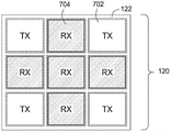
FIG. 2A illustrates a simplified exemplary array of sensor elements that may be used in the input device of FIG. 1.
FIG. 2B illustrates an alternative array of sensor elements that may be used in the input device of FIG. 1.
FIG. 2C illustrates an alternative array of sensor elements that may be used in the input device of FIG. 1.
FIG. 2D illustrates yet another alternative array of sensor elements that may be used in the input device of FIG. 1.
Fig. 3 is a simplified cross-sectional view of the sensor element of fig. 1, showing the active portion of the sensor electrode aligned with a pixel element of the display.
FIG. 4 is a simplified cross-sectional view of another embodiment of the sensor assembly of FIG. 1 showing a grid electrode offset over the sensor electrodes.
FIG. 5 is a simplified cross-sectional view of yet another embodiment of the sensor assembly of FIG. 1, showing a grid electrode offset over the sensor electrodes, with some of the sensor electrodes aligned with the grid electrodes.
FIG. 6 is a simplified schematic plan view of a sensor element operating in a transcapacitive mode.
FIG. 7 is another simplified schematic plan view of a sensor element operating in a transcapacitive mode.
FIG. 8 is a flow diagram of one embodiment of a method for detecting the presence of an input object.
FIG. 9 is a flow diagram of another embodiment of a method for detecting the presence of an input object.
FIG. 10 is a flow diagram of yet another embodiment of a method for detecting the presence of an input object.
FIG. 11 is an exploded side view of one embodiment of an exemplary display device with an integrated input device showing alternative locations for grid electrodes.
Fig. 12A-12E illustrate various different shapes of sensor electrodes and grid electrodes.
To facilitate understanding, identical reference numerals have been used, where possible, to designate identical elements that are common to the figures. It is contemplated that elements disclosed in one embodiment may be beneficially utilized on other embodiments without recitation. The drawings referred to herein should not be understood as being drawn to scale unless specifically noted. Additionally, the drawings are generally simplified and details or components are omitted for clarity of presentation and description. The drawings and discussion are intended to illustrate the principles described below, wherein like reference numerals refer to like elements.
Detailed Description
The following detailed description is merely exemplary in nature and is not intended to limit the invention or the application and uses of the invention. Furthermore, there is no intention to be bound by any expressed or implied theory presented in the preceding technical field, background, brief summary or the following detailed description.
Various embodiments of the present technology provide input devices and methods for improving usability. In particular, embodiments described herein advantageously utilize absolute sensing techniques to provide good input object positions in the sensing region, even in applications where multiple input objects are present or when the input objects are in motion. Additionally, some other embodiments provide for switching between absolute and transcapacitive sensing modes, thus allowing the appropriate sensing mode to be used to optimally determine the position and motion of one or more objects in the sensing region.
FIG. 1 is a schematic block diagram of an input device 100 in accordance with embodiments of the present technique. In one embodiment, the input device 100 includes a display device with an integrated sensing device. Although the illustrated embodiments of the present disclosure are illustrated as being integrated with a display device, it is contemplated that the present invention may be implemented in an input device that is not integrated with a display device. The input device 100 may be configured to provide input to an electronic system 150. The term "electronic system" (or "electronic device"), as used in this document, broadly refers to any system capable of electronically processing information. Some non-limiting examples of electronic systems include personal computers of all sizes and shapes, such as desktop computers, laptop computers, netbook computers, tablets, web browsers, e-book readers, and Personal Digital Assistants (PDAs). Additional example electronic systems include composite input devices, such as a physical keyboard including input device 100 and a separate joystick or key switch. Other example electronic systems include peripherals such as data input devices (including remote controls and mice) and data output devices (including display screens and printers). Other examples include remote terminals, kiosks, and video game machines (e.g., video game consoles, portable gaming devices, etc.). Other examples include communication devices (including cellular telephones, such as smart phones) and media devices (including recorders, editors, and players (such as televisions, set-top boxes, music players, digital photo frames, and digital cameras)). In addition, the electronic system may be a master or a slave of the input device.
The input device 100 can be implemented as a physical part of an electronic system or can be physically separated from the electronic system. Suitably, the input device 100 may communicate with portions of the electronic system using any one or more of the following: buses, networks, and other wired or wireless interconnections. Examples include I2C. SPI, PS/2, Universal Serial Bus (USB), Bluetooth, RF, and IRDA.
In FIG. 1, the input device 100 is shown as a proximity sensor device (also often referred to as a "touchpad" or a "touch sensor device") configured to sense input provided by one or more input objects 140 in a sensing region 170. Example input objects include fingers and styli, as shown in FIG. 1.
The sensing region 170 encompasses any space above, around, in, and/or near the input device 100 in which the input device 100 is capable of detecting user input (e.g., user input provided by one or more input objects 140). The size, shape, and location of a particular sensing region may vary greatly from embodiment to embodiment. In some embodiments, the sensing region 170 extends in one or more directions into space from the surface of the input device 100 until the signal-to-noise ratio prevents sufficiently accurate object detection. In various embodiments, the distance that this sensing region 170 extends in a particular direction may be on the order of less than a millimeter, millimeters, centimeters, or more, and may vary greatly depending on the type of sensing technology used and the accuracy desired. Thus, some embodiments sense input that includes not being in contact with any surface of input device 100, being in contact with an input surface (e.g., a touch surface) of input device 100, being in contact with an input surface of input device 100 coupled with an amount of applied force or pressure, and/or combinations thereof. In various embodiments, the input surface may be provided by a surface of the housing in which the sensor electrodes are located, by a panel applied over the sensor electrodes or any housing, or the like. In some embodiments, the sensing region 170 has a rectangular shape when projected onto an input surface of the input device 100.
The input device 100 may utilize any combination of sensor components and sensing technologies to detect user input in the sensing region 170. The input device 100 includes a plurality of sensing elements 124 for detecting user inputs. Sensing element 124 includes a plurality of sensor electrodes 120 and one or more grid electrodes 122. As a number of non-limiting examples, input device 100 may use capacitive, inverted dielectric, resistive, inductive, magnetic, acoustic, ultrasonic, and/or optical technologies.
Some implementations are configured to provide images that span one, two, three, or higher dimensional spaces. Some implementations are configured to provide projection of an input along a particular axis or plane.
In some resistive implementations of the input device 100, the flexible and conductive first layers are separated from the conductive second layer by one or more spacer elements. During operation, one or more voltage gradients are created across the multiple layers. Pressing the flexible first layer may deflect it sufficiently to create electrical contact between the multiple layers, thereby producing a voltage output that reflects the point of contact between the multiple layers. These voltage outputs may be used to determine position information.
In some inductive implementations of the input device 100, one or more sensing elements 124 obtain a loop current induced by a resonant coil or coil pair. Some combination of the amplitude, phase and frequency of the current may then be used to determine position information.
In some capacitive implementations of input device 100, a voltage or current is applied to create an electric field. Nearby input objects cause a change in the electric field and produce a detectable change in the capacitive coupling, which can be detected as a change in voltage, current, etc.
Some capacitive implementations utilize an array or other regular or irregular pattern of capacitive sensing elements 124 to create an electric field. In some capacitive implementations, the individual sensing elements 124 may be ohmically shorted together to form larger sensor electrodes. Some capacitive implementations utilize resistive patches, which may be uniformly resistive.
As described above, some capacitive implementations utilize a "self-capacitance" or (or "absolute capacitance") sensing method that is based on changes in the capacitive coupling between the sensor electrodes 120 and the input object. In various embodiments, an input object near the sensor electrode 120 changes the electric field near the sensor electrode 120, thus changing the measured capacitive coupling. In one implementation, the absolute capacitive sensing method operates by modulating the sensor electrode 120 relative to a reference voltage (e.g., system ground) and by detecting capacitive coupling between the sensor electrode 120 and the input object 140.
Additionally, as described above, some capacitive implementations utilize a "mutual capacitance" (or "transcapacitive") sensing method that is based on changes in the capacitive coupling between the sensor electrodes 120. In various embodiments, an input object 140 near the sensor electrodes 120 alters the electric field between the sensor electrodes 120, thus altering the measured capacitive coupling. In one implementation, the transcapacitive sensing method operates by: capacitive coupling between one or more transmitter sensor electrodes (also referred to as "transmitter electrodes") and one or more receiver sensor electrodes (also referred to as "receiver electrodes") is detected, as described further below. The transmitter sensor electrode may be modulated relative to a reference voltage (e.g., system ground) to transmit a transmitter signal. The receiver sensor electrodes may be held substantially constant relative to a reference voltage to facilitate reception of the generated signal. The generated signal may include the effect(s) corresponding to one or more transmitter signals and/or to one or more sources of environmental interference (e.g., other electromagnetic signals). The sensor electrodes 120 may be dedicated transmitter electrodes or receiver electrodes, or may be configured to both transmit and receive.
In fig. 1, the processing system 110 is shown as part of the input device 100. The processing system 110 is configured to operate the hardware of the input device 100 to detect input in the sensing region 170. Processing system 110 includes some or all of one or more Integrated Circuits (ICs) and/or other circuit components. (e.g., a processing system of a mutual capacitance sensor device may include a transmitter circuit configured to transmit signals using a transmitter sensor electrode and/or a receiver circuit configured to receive signals using a receiver sensor electrode.) in some embodiments, the processing system 110 also includes electronically readable instructions, such as firmware code, software code, or the like. In some embodiments, the components making up the processing system 110 are co-located, for example, in the vicinity of the sensing element(s) 124 of the input device 100. In other embodiments, the components of the processing system 110 are physically independent, with one or more components proximate to the sensing element(s) 124 of the input device 100 and one or more components at other locations. For example, the input device 100 may be a peripheral coupled to a desktop computer, and the processing system 110 may include software configured to run on a central processing unit of the desktop computer and one or more ICs (perhaps with associated firmware) separate from the central processing unit. As another example, the input device 100 may be physically integrated into a phone, and the processing system 110 may include circuitry and firmware that are part of the main processor of the phone. In some embodiments, the processing system 110 is dedicated to implementing the input device 100. In other embodiments, the processing system 110 also performs other functions, such as operating a display screen, driving haptic actuators, and the like.
The processing system 110 may be implemented as a set of modules that handle different functions of the processing system 110. The modules may include circuitry, firmware, software, or a combination thereof, which are part of the processing system 110. In various embodiments, different combinations of modules may be used. An example module includes: a hardware operation module for operating hardware such as sensor electrodes and a display screen; a data processing module for processing data such as sensor signals and location information; and a reporting module for reporting the information. Other example modules include: a sensor operation module configured to operate the sensing element(s) 124 to detect an input; a recognition module configured to recognize a gesture such as a mode change gesture; and a mode change module for changing the operation mode.
In some embodiments, the processing system 110 responds to user input (or lack thereof) in the sensing region 170 directly by causing one or more actions. Example actions include changing operating modes and GUI actions such as cursor movement, selection, menu navigation, and other functions. In some embodiments, the processing system 110 provides information about the input (or lack thereof) to some portion of the electronic system (e.g., to a central processing system of the electronic system that is separate from the processing system 110, if such a separate central processing system exists). In some embodiments, some portion of the electronic system processes information received from the processing system 110 to act on user input, such as to facilitate a full series of actions, including mode change actions and GUI actions.
For example, in some embodiments, the processing system 110 operates the sensing element(s) 124 of the input device 100 to generate electrical signals that are indicative of input (or lack thereof) in the sensing region 170. The processing system 110 may perform any suitable amount of processing on the electrical signals in generating the information provided to the electronic system. For example, the processing system 110 may digitize the resulting analog electrical signal from the sensing element 124. As another example, the processing system 110 may perform filtering, demodulation, or other signal conditioning. In various embodiments, the processing system 110 generates a capacitance image directly from the resulting signals received with the sensing elements 124 (sensor electrodes 120). In other embodiments, processing system 110 spatially filters (e.g., takes the difference, weighted sum of neighboring elements) the resulting signals received with sensing elements 124 (or sensor electrodes 120) to generate a sharpened or averaged image. As yet another example, the processing system 110 may subtract or otherwise consider the reference such that the information reflects a difference between the electrical signal and the reference. As still further examples, the processing system 110 may determine location information, recognize an input as a command, recognize handwriting, and so forth.
"position information" as used herein broadly includes absolute position, relative position, velocity, acceleration, and other types of spatial information. Exemplary "zero-dimensional" location information includes near/far or contact/no-contact information. Exemplary "one-dimensional" position information includes position along an axis. Exemplary "two-dimensional" positional information includes motion in a plane. Exemplary "three-dimensional" position information includes instantaneous or average velocity in space. Other examples include other representations of spatial information. Historical data relating to one or more types of location information may also be determined and/or stored, including, for example, historical data that tracks location, motion, or instantaneous speed over time.
In some embodiments, the input device 100 is implemented with additional input components operated by the processing system 110 or by some other processing system. These additional input components may provide redundant functionality for input in the sensing region 170 or some other functionality. FIG. 1 shows buttons 130 near a sensing region 170 that can be used to facilitate selection of items using the input device 100. Other types of additional input components include sliders, balls, wheels, switches, and the like. Conversely, in some embodiments, the input device 100 may be implemented without other input components.
In some embodiments, the input device 100 includes a touch screen interface and the sensing region 170 overlaps at least a portion of an active area of a display screen of the display device 160. For example, the input device 100 may include a substantially transparent sensing element 124 overlying a display screen and providing a touch screen interface for an associated electronic system. The display screen may be any type of dynamic display capable of displaying a visual interface to a user, and may include any type of Light Emitting Diode (LED), organic LED (oled), Cathode Ray Tube (CRT), Liquid Crystal Display (LCD), plasma, electro-luminescence (EL), or other display technology. The input device 100 and the display device 160 may share physical elements. For example, some embodiments can use a portion of the same electrical components for display and sensing (e.g., active matrix control electrodes configured to control source, gate, and/or Vcom voltages). The shared components may include display electrodes, substrates, connectors, and/or connections. As another example, the display device 160 may be partially or fully operated by the processing system 110.
It should be understood that while many embodiments of the present technology are described in the context of fully functioning devices, the mechanisms of the present technology are capable of being distributed as a program product (e.g., software) in a variety of forms. For example, the mechanisms of the present technology may be implemented and distributed as a software program on an information bearing medium readable by an electronic processor (e.g., a non-transitory computer-readable and/or recordable/writable information bearing medium readable by the processing system 110). In addition, embodiments of the present technology are equally applicable regardless of the particular type of medium used to perform the distribution. Examples of non-transitory electronically readable media include various optical disks, memory sticks, memory cards, memory modules, and the like. The electronically readable medium may be based on flash, optical, magnetic, holographic or any other storage technology.
Fig. 2A illustrates a portion of an exemplary pattern of sensing elements 124 configured to sense in a sensing region 170 associated with the pattern, according to some embodiments. For clarity of illustration and description, fig. 2A shows the sensor electrodes 120 of the sensing element 124 in a simple rectangular pattern with the grid electrode 222 disposed between the sensor electrodes, and without showing various other components. An exemplary pattern of sensing elements 124 includes sensor electrodes 120 arranged in X columns and Y rowsX,YWhere X and Y are positive integers, but one of X and Y may be zero (collectively referred to as sensor electrodes 120). It is contemplated that the pattern of sensing elements 124 may include a plurality of sensor electrodes 120 having other configurations (e.g., polar array, repeating pattern, non-repeating pattern, single row or column, or other suitable arrangement). Further, in various embodiments, the number of sensor electrodes may vary from row to row and/or column to column. In one embodiment, at least one row and/or column of sensor electrodes 120 is offset from the other sensor electrodes such that it extends further in at least one direction than the other sensor electrodes. The sensor electrodes 120 and the grid electrodes 122 are coupled to the processing system 110 and are used to determine the presence (or absence) of an input object 140 in the sensing region 170.
In a first mode of operation, the arrangement of sensor electrodes 120(120-1, 120-2, 120-3, …, 120-n) may be used to detect the presence of an input object via absolute sensing techniques. That is, the processing system 110 is configured to modulate the sensor electrode 120 to obtain a measure of a change in the capacitive coupling between the modulated sensor electrode 120 and the input object to determine the position of the input object. The processing system 110 is further configured to determine a change in absolute capacitance based on a measurement of the resulting signal received with the sensor electrode 120 (which is modulated).
The sensor electrodes 120 are typically ohmically isolated from each other and also from the grid electrodes 122. That is, one or more insulators separate the sensor electrodes 120 (and the mesh electrodes 122) and prevent them from electrically shorting to each other. In some embodiments, sensor electrode 120 and grid electrode 122 are separated by an insulating gap 202. The insulating gap 202 separating the sensor electrode 120 and the grid electrode 122 may be filled with an electrically insulating material, or may be an air gap. In some embodiments, sensor electrode 120 and grid electrode 122 are vertically separated by one or more layers of insulating material. In certain other embodiments, sensor electrode 120 and grid electrode 122 are separated by one or more substrates; for example, they may be disposed on opposite sides of the same substrate or on different substrates. In still other embodiments, grid electrode 122 may be composed of multiple layers on the same substrate or on different substrates. In one embodiment, the first mesh electrode may be formed on a first substrate or a first side of the substrate, and the second mesh electrode may be formed on a second substrate or a second side of the substrate. For example, the first grid includes one or more common electrodes disposed on a TFT layer of the display device 160, and the second grid electrode is disposed on a color filter glass of the display device 160. In one embodiment, the size of the first grid electrode is equal to the size of the second grid electrode. In one embodiment, at least one dimension of the first grid electrode is different from a dimension of the second grid electrode. For example, the first grid electrode may be configured such that it is disposed between the first and second sensor electrodes 120, and the second grid electrode may be configured such that it overlaps at least one of the first and second sensor electrodes 120 and the first grid electrode. Furthermore, the first grid electrode may be configured such that it is disposed between the first and second sensor electrodes 120, and the second grid electrode may be configured such that it overlaps only the first grid electrode and is smaller than the first grid electrode.
In a second mode of operation, sensor electrodes 120(120-1, 120-2, 120-3, …, 120-n) may be used to detect the presence of an input object via a transcapacitive sensing technique when a transmitter signal is driven onto grid electrode 122. That is, the processing system 110 is configured to drive the grid electrodes 122 with the transmitter signals and receive the resulting signals with the sensor electrodes 120, where the resulting signals contain an effect corresponding to the transmitter signals, which are used by the processing system 110 or another processor to determine the position of the input object.
In a third mode of operation, the sensor electrodes 120 may be divided into groupings of transmitter and receiver electrodes to detect the presence of an input object via transcapacitive sensing techniques. That is, the processing system 110 may employ the transmitter signal to drive the first set of sensor electrodes 120 and the second set of sensor electrodes 120 to receive the generated signal, where the generated signal includes an effect corresponding to the transmitter signal. The resulting signals are used by the processing system 110 or another processor to determine the position of the input object.
The input device 100 may be configured to operate in any of the above-described modes. Input device 100 may also be configured to switch between any two or more of the above-described modes.
The area of local capacitive sensing of capacitive coupling may be referred to as a "capacitive pixel". Capacitive pixels may be formed between individual sensor electrodes 120 and a reference voltage in a first mode of operation, between sensor electrodes 120 and grid electrodes 122 in a second mode of operation, and between groupings of sensor electrodes 120 that serve as transmitter and receiver electrodes. The capacitive coupling varies with the proximity and motion of an input object 140 in the sensing region 170 associated with the sensing element 124, and thus may be used as an indicator of the presence of an input object in the sensing region of the input device 100.
In some embodiments, the sensor electrodes 120 are "scanned" to determine these capacitive couplings. That is, in one embodiment, one or more of the sensor electrodes 120 are driven to transmit a transmitter signal. The transmitter may be operated such that one transmitter electrode transmits at a time, or multiple transmitter electrodes transmit simultaneously. In the case of multiple transmitter electrodes transmitting simultaneously, multiple transmitter electrodes may transmit the same transmitter signal and in fact result in a substantially larger transmitter electrode. Alternatively, multiple transmitter electrodes may transmit different transmitter signals. For example, multiple transmitter electrodes may transmit different transmitter signals according to one or more coding schemes that enable the combined effect of the transmitter signals on the resulting signals of the receiver electrodes to be determined individually. In one embodiment, multiple transmitter electrodes may transmit the same transmitter signal simultaneously, while the receiver electrodes employ a scanning scheme for reception.
The sensor electrodes 120 configured as receiver sensor electrodes may be operated singly or plurally to acquire the resulting signals. The generated signal may be used to determine a measure of capacitive coupling at the capacitive pixel. The processing system 110 may be configured to receive with the sensor electrodes 120 in a scanning and/or multiplexing manner to reduce the number of simultaneous measurements to be made and the size of the supporting electrical structure. In one embodiment, one or more sensor electrodes are coupled to a receiver of the processing system 110 via a switching element, such as a multiplexer or the like. In such embodiments, the switching element may be internal to the processing system 110 or external to the processing system 110. In one or more embodiments, the switching element can also be configured to couple the sensor electrode with a transmitter or other signal and/or voltage potential. In one embodiment, the switching element may be configured to simultaneously couple more than one receiver electrode to a common receiver.
In other embodiments, "scanning" the sensor electrodes 120 to determine these capacitive couplings includes modulating one or more of the sensor electrodes and measuring the absolute capacitance of one or more of the sensor electrodes. In another embodiment, the sensor electrodes may be operated such that more than one sensor electrode is driven and receiving at the same time. In such embodiments, the absolute capacitance measurements may be taken from each of the one or more sensor electrodes 120 simultaneously.
In one embodiment, each of the sensor electrodes 120 is driven and configured to receive simultaneously, thereby obtaining an absolute capacitance measurement from each of the sensor electrodes 120 simultaneously. In various embodiments, processing system 110 may be configured to selectively modulate a portion of sensor electrodes 120. For example, the sensor electrodes may be selected based on, but not limited to, an application running on the main processor, a state of the input device, and an operating mode of the sensing device. In various embodiments, processing system 110 may be configured to selectively shield at least a portion of sensor electrodes 120, and to selectively shield or grid electrode(s) 122 or transmit with grid electrode(s) 122 while selectively receiving and/or transmitting with other sensor electrodes 120.
A set of measurements from the capacitive pixels forms a "capacitive image" (also referred to as a "capacitive frame") that represents the capacitive coupling at the pixel. Multiple capacitive images may be acquired for multiple time periods, and the differences between them used to derive information about input in the sensing region. For example, successive capacitive images acquired for successive time periods can be used to track motion of one or more input objects entering, exiting, and within the sensing region.
In any of the above embodiments, multiple sensor electrodes 120 may be bonded together such that the sensor electrodes 120 are modulated or simultaneously available for reception. As compared to the methods described above, combining multiple sensor electrodes together can produce a process (course) capacitance image that cannot be used to discern accurate position information. However, the process capacitance image may be used to sense the presence of an input object. In one embodiment, the process capacitance image may be used to bring the processing system 110 or the input device 100 out of a sleep or low power mode. In one embodiment, the process capacitance image may be used to bring the capacitive sensor integrated circuit out of a sleep mode or low power mode. In another embodiment, the process capacitance map may be used to bring the primary integrated circuit out of a sleep mode or low power mode. The process capacitance image may correspond to the entire sensor area, or only a portion of the sensor area.
The background capacitance of the input device 100 is a capacitive image associated with no input objects in the sensing region 170. The background capacitance varies with the environment and operating conditions and can be estimated in a number of ways. For example, some embodiments acquire "reference images" when it is determined that no input object is in the sensing region 170, and use those reference images as estimates of their background capacitance. Background or reference capacitance may exist due to stray capacitive coupling between two sensor electrodes (where one sensor electrode is driven with a modulation signal while the other sensor electrode remains fixed relative to system ground) or from stray capacitive coupling between a receiver electrode and a nearby modulation electrode. In many embodiments, the background or reference capacitance may be relatively fixed for the time period of the user input gesture.
The capacitance image can be adjusted for the background capacitance of the input device 100 for more efficient processing. Some embodiments accomplish this by "baselining" the measurement of capacitive coupling at the capacitive pixels to produce a "baselined capacitive image". That is, some embodiments compare the measurement forming the capacitance image to an appropriate "reference value" of a "reference image" associated with those pixels, and determine the change from that reference image.
In some touch screen embodiments, one or more of the sensor electrodes 120 include one or more display electrodes used in updating the display of the display screen. The display electrodes can comprise one or more elements of an active matrix display, such as one or more segments of a segmented Vcom electrode (common electrode (s)), a source drive line, a gate line, an anode sub-pixel electrode or a cathode pixel electrode, or any other display element. These display electrodes may be provided on a suitable display screen substrate. For example, the common electrode may be disposed on a transparent substrate (glass substrate, TFT glass, or any other transparent material) in some display screens (e.g., in-plane switching (IPS), Fringe Field Switching (FFS), or Planar Line Switching (PLS) Organic Light Emitting Diodes (OLEDs)), the bottom of a color filter glass of some display screens (e.g., Patterned Vertical Alignment (PVA) or multi-domain vertical alignment (MVA)), over an emission layer (OLED), and the like. In such embodiments, the display electrode can again be referred to as a "combination electrode" because it performs multiple functions. In various embodiments, each of the sensor electrodes 120 includes one or more common electrodes. In other embodiments, at least two sensor electrodes 120 may share at least one common electrode. Although the following description may describe sensor electrodes 120 and/or grid electrodes 122 as including one or more common electrodes, various other display electrodes, as described above, may also be used in conjunction with or as an alternative to common electrodes. In various embodiments, sensor electrode 120 and grid electrode 122 comprise the entire common electrode layer (Vcom electrode).
In various touch screen embodiments, the "capacitive frame rate" (the rate at which successive capacitive images are acquired) and the "display frame rate" (the rate at which display images are updated, including refreshing the screen to redisplay the same image) may be the same or different. In various embodiments, the capacitive frame rate is an integer multiple of the display frame rate. In other embodiments, the capacitive frame rate is a fractional multiple of the display frame rate. In still other embodiments, the capacitive frame rate may be any fraction or integer of the display frame rate. In one or more embodiments, the display frame rate may be varied while the touch frame rate remains constant (e.g., to reduce power or provide additional image data, such as 3D display information). In other embodiments, the display frame rate may be kept constant while the touch frame rate is increased or decreased.
With continued reference to fig. 2A, the processing system 110 coupled to the sensor electrodes 120 includes a sensor module 204 and an optional display driver module 208. The sensor module 204 includes circuitry configured to drive at least one of the sensor electrodes 120 for capacitive sensing during periods of expected input sensing. In one embodiment, the sensor module is configured to drive a modulation signal onto the at least one sensor electrode to detect a change in absolute capacitance between the at least one sensor electrode and the input object. In another embodiment, the sensor module is configured to drive a transmitter signal onto at least one sensor electrode to detect a change in transcapacitance between the at least one sensor electrode and another sensor electrode. The modulation and transmitter signals are typically varying voltage signals that contain a plurality of voltage transitions for the time period allotted for input sensing. In various embodiments, sensor electrodes 120 and/or grid electrodes 122 may be driven in different ways in different modes of operation. In one embodiment, sensor electrodes 120 and/or grid electrodes 122 may be driven with signals (modulation signals, transmitter signals, and/or shielding signals) that may differ in any of phase, amplitude, and/or shape. In various embodiments, the three modulation signals and the transmitter signal are similar in at least one of shape, frequency, amplitude, and/or phase. In other embodiments, the modulation signal and the transmitter signal are different in frequency, shape, phase, amplitude, and phase. Sensor module 204 may selectively couple one or more of sensor electrodes 120 and/or grid electrodes 122. For example, sensor module 204 may be coupled to a selected portion of sensor electrodes 120 and operate in an absolute or transcapacitive sensing mode. In another example, sensor module 204 may be a different portion of sensor electrode 120 and operate in an absolute or transcapacitive sensing mode. In yet another example, sensor module 204 may be coupled to all sensor electrodes 120 and operate in an absolute or transcapacitive sensing mode. The sensor module 204 is also configured to operate the grid electrode 122 as a shield electrode. Processing system 110 is configured to operate grid electrode 122 as a shield electrode that can shield sensor electrode 120 from electrical effects of nearby conductors. In one embodiment, the processing system is configured to operate grid electrode 12 as a shield electrode that can shield sensor electrode 120 from electrical effects of nearby conductors and protect sensor electrode 120 from grid electrode 122, thereby at least partially reducing parasitic capacitance between grid electrode 122 and sensor electrode 120. In one embodiment, the shield signal is driven onto the grid electrode 122. The masking signal may be a ground signal, such as system ground or another ground, or may be any other constant voltage (i.e., non-modulated) signal. In another embodiment, operating the grid electrode 122 as a shield electrode may include electrically floating the grid electrode. In an embodiment, the grid electrode 122 is capable of operating as an effective shield electrode while being electrode floating due to its large coupling with other sensor electrodes. In other embodiments, the masking signal may be referred to as a guard signal, where the guard signal is a varying voltage signal having at least one of a similar phase, frequency, and amplitude as the modulation signal driven onto the sensor electrodes. In one or more embodiments, the wiring (e.g., traces 240 and/or 242) may be shielded from responding to input objects due to the wiring under grid electrodes 122 and/or sensor electrodes 120, and thus may not be an integral part of the active sensor electrodes shown as sensor electrodes 120.
In one or more embodiments, the capacitive sensing (or input sensing) and display updating may occur during periods that at least partially overlap. For example, when driving the common electrode for display updating, the common electrode may also be driven for capacitive sensing. In another embodiment, the capacitive sensing and display update may occur during non-overlapping periods (also referred to as non-display update periods). In various embodiments, the non-display update period may occur between display line update periods of two display lines of a display frame and may have at least as long a time as the display update period. In such embodiments, the non-display update period may be referred to as a long horizontal blanking period, a long h blanking period, or a distributed blanking period, where the blanking period occurs between two display update periods and is at least as long as the display update period. In one embodiment, the non-display update periods occur between display line update periods of a frame and are long enough to allow multiple transitions of the transmitter signal driven onto the sensor electrodes 120. In other embodiments, the non-display update period may include a horizontal blanking period and a vertical blanking period. The processing system 110 may be configured to drive the sensor electrodes 120 for capacitive sensing during any one or more or any combination of different non-display update times. Synchronization signals may be shared between the sensor module 204 and the display module 208 to provide accurate control of overlapping display updates and capacitive sensing cycles at repeatable coherent frequencies and phases. In one embodiment, these synchronization signals may be configured to allow the more stable voltages at the beginning and end of the input sensing period to coincide with a display update period having a more stable voltage (e.g., near the end of the input integrator reset time and near the end of the display charge sharing time). The modulation frequency of the modulation or transmitter signal may be at a harmonic of the display line update rate, with the phase determined to provide a near constant charge coupling from the display element to the receiver electrode, allowing this coupling to be part of the reference image.
The sensor module 204 includes circuitry configured to employ the sensing element 124 to receive a generated signal containing an effect corresponding to a modulated signal or a transmitter signal during a period of intended input sensing. The sensor module 204 may determine the position of the input object 140 in the sensing region 170, or may provide a signal containing information indicative of the generated signal to another module or processor, such as a processor (i.e., a host processor) or determination module of the electronic device 150, for determining the position of the input object 140 in the sensing region 170.
The display driver module 208 may be included in the processing system 110 or separate therefrom. The display driver module 208 includes circuitry that determines to provide display image update information to the display of the display device 160 during non-sensing (e.g., display update) periods. In one embodiment, the sensor module 204 and the display module 208 may be included in a common integrated circuit (first controller). In another embodiment, two of the sensor module 204, and the display module 208 are included in a first integrated circuit, and another of the three modules is included in a second integrated circuit. In those embodiments that include multiple integrated circuits, a synchronization mechanism may be coupled therebetween that is configured to synchronize the display update period, the sensing period, the transmitter signal, the display update signal, and the like.
As described above, the sensor electrodes 120 of the sensing element 124 may be formed in discrete geometric forms, polygons, bars, blocks, lines, or other shapes, with the sensor electrodes ohmically isolated from each other. In various embodiments, ohmic isolation includes passive isolation, wherein an active switch may be configured to couple different sensor electrodes to the same signal during a certain time period. Sensor electrodes 120 may be electrically coupled by a circuit to form an electrode having a larger planar area relative to the individual sensor electrodes in sensor electrodes 120. The sensor electrodes 120 may be fabricated from opaque or transparent conductive materials or a combination of both. In embodiments where sensor electrodes 120 are used in conjunction with a display device, it may be desirable to use a transparent conductive material for sensor electrodes 120. In embodiments where sensor electrodes 120 are not used with a display device, it may be desirable to use an opaque conductive material with a lower resistivity for sensor electrodes 120 to improve sensor performance. Suitable materials for making the sensor electrodes 120 include ITO, aluminum, silver, copper, molybdenum, and conductive carbon materials, among others, and the various sensor electrodes may be formed from deposited stacks of different conductive materials. The sensor electrodes 120 may be formed as a continuous body of conductive material with little or no open area (i.e., having a planar surface uninterrupted by holes), or alternatively may be fabricated to form an object of material having openings formed therethrough. For example, the sensor electrode 120 may be formed from a wire mesh of conductive material, such as a plurality of interconnected thin metal wires. In one embodiment, at least one of the length and width of the sensor electrode 120 may be in the range of about 1 to about 2 mm. In other embodiments, at least one of the length and width of the sensor electrode may be less than about 1mm or greater than about 2 mm. In other embodiments, the length and width may not be similar, and one of the length and width may be in the range of about 1 to about 2 mm. Further, in various embodiments, the sensor electrodes 120 may include a center-to-center spacing in the range of about 4 to about 5 mm; however, in other embodiments, the spacing may be less than about 4mm or greater than about 5 mm.
A grid electrode 122 is disposed between at least two of the sensor electrodes 120. The grid electrode 122 may at least partially surround (circumscribes) the plurality of sensor electrodes 120 as a group, and may also (or alternatively) completely or partially surround one or more of the sensor electrodes 120. In one embodiment, grid electrode 122 is a planar object 212 having a plurality of apertures 210, each aperture 210 surrounding a respective one of sensor electrodes 120. Accordingly, grid electrodes 122 separate and surround at least 3 or more of sensor electrodes 120, and in this example, all of sensor electrodes 120. The gap 202 spaces the object 212 from the sensor electrode 120 disposed in the aperture 210. In one or more embodiments, the field electrodes 122 are configured to substantially fill the space defined by the spacing 202. In one embodiment, the second grid electrode may be disposed on the substrate between the grid electrode 122 and the touch input layer. The second grid electrode may be the same size as grid electrode 122 or larger than grid electrode 122 such that it overlaps one or more sensor electrodes 120 and grid electrode, or smaller than grid electrode 122 such that it overlaps a portion of grid electrode 122. In various embodiments, the grid electrode 122 is disposed between at least two of the sensor electrodes 120 such that the grid electrodes 122 are on different layers (i.e., different substrates or different sides of the same substrate) and overlap a portion of at least two sensor electrodes and a gap between the sensor electrodes. In embodiments where the sensor electrode 120 includes one or more common electrodes, the sensor electrode may include the entirety of the common electrode layer.
The grid electrode 122 may also be segmented. The segmentation of the grid electrode 122 may allow the segments of the grid electrode 122 to be less visible. The segments may be interconnected using traces or vias such that all segments of the mesh electrode 122 may be driven simultaneously with a common signal. Alternatively, one or more of the segments of grid electrode 122 may be driven individually to facilitate scanning of sensor electrode 120 when sensor electrode 120 is configured as a receiver electrode in certain modes of operation, as discussed further below.
As shown in the enlarged view of fig. 2A, the grid electrode122 may include a first section 230, a second section 232, and a third section 234. The first and second segments 230, 232 are offset from each other and sandwich a column of sensor electrodes, shown as sensor electrode 1202,1、1022,2. Although not shown in the enlarged view, the first segment 230 also connects the sensor electrode column 1202,YAnd the sensor electrode 1021,YSeparated, and a second segment 232 separating the sensor electrode columns 1202,YAnd the sensor electrode 1023,YAnd (4) separating. The third segment 234 is disposed adjacent sensor electrodes 120 in a column (shown as sensor electrodes 120)2,1、1022,2) In the meantime. Two or more of the segments 230, 232, 234 may be driven individually, for example as transmitter electrodes.
FIG. 2B illustrates an alternative array of sensor elements 124 that may be used in the input device 100 of FIG. 1. As shown in fig. 2B, sensor element 124 includes a grid electrode 122, which may include a substantially larger surface area than sensor electrode 120. In the embodiment of fig. 2B, mesh electrode 122 at least partially surrounds one or more sensor electrodes 120, for example as indicated with reference to arrow 290. Additionally or alternatively, the grid electrode 122 completely surrounds at least one sensor electrode 120 and only partially surrounds the other sensor electrodes 120, for example as shown with reference to arrows 290 and 292. In other embodiments, grid electrode 122 may completely surround all sensor electrodes 120. Although not shown in fig. 2B, it is contemplated that the grid electrode 122 may be segmented as described with reference to fig. 2A.
FIG. 2C illustrates an alternative array of sensor elements 124 that may be used in the input device 100 of FIG. 1. As shown in FIG. 2C, sensor element 124 includes more than one grid electrode, collectively referred to as grid electrode 122 and illustratively shown as grid electrode 122(A,B)Wherein A and B are non-zero integers. In the embodiment of fig. 2C, each grid electrode 122 at least partially surrounds a different set of sensor electrodes 120, wherein a set of sensor electrodes is defined as a set of sensor electrodes at least partially surrounded by a common grid electrode of the grid electrodes 122. Each grid electrode 122 may be substantially similar in size and surround the same number of sensor electrodes 120; however, in other embodiments, the grid electrode 122 may be largerAt least one aspect of the number of small and sensor electrodes 120 at least partially enclosed may vary. Furthermore, although the embodiment of fig. 2C shows eight grid electrodes 122, in other embodiments, the input device 100 may include two or more grid electrodes 122. In one embodiment, each mesh electrode 122 may be via what is shown as trace 242(1,1)、242(1,B)、242(A,1)And 242(A,B)Are separately coupled to the processing system 110. In other embodiments, two or more mesh electrodes 122 may be coupled to the processing system 110 via a common conductive routing trace 242, in other words, trace 242(1,1)、242(1,B)、242(A,1)And 242(A,B)Are combined together. In such an embodiment, a multiplexer (or similar circuit) may be used to switch between the grid electrodes 122.
The plurality of grid electrodes 122 may be arranged in an orientation having an aerial extent that extends further in a first direction than a second direction, the second direction being orthogonal to the first direction. In one embodiment, each grid electrode 122 is disposed in an orientation having an aerial extent that extends further in the first direction than the second direction. In another embodiment, each grid electrode 122 is disposed in an orientation having an aerial extent that extends further in the second direction than the first direction. In still other embodiments, each grid electrode 122 is disposed in an orientation having an aerial extent that extends substantially the same distance in the first and second directions. Further, the grid electrodes 122 may be configured such that one or more grid electrodes 122 have an aerial extent that is oriented differently than at least one other grid electrode 122. For example, the first grid electrode 122 may extend further in the first direction than the second direction, and the second grid electrode 122 may extend further in the second direction than the first direction. In other examples, other combinations of grid electrode 122 orientations are possible. In other embodiments, grid electrodes 122 may be oriented such that the size of each grid electrode 122 is substantially similar. At least one of the sensor electrodes 120 or the set of sensor electrodes 120 may be similarly configured as described with reference to the grid electrodes 122.
In some embodiments, the sets of sensor electrodes 120 surrounded by a single grid electrode 122 may be aligned in a single row. In other embodiments, the set of sensor electrodes 120 surrounded by a single grid electrode 122 may be linearly aligned in a single row, such as shown in the embodiment shown in fig. 2C. In still other embodiments, the sets of sensor electrodes 120 surrounded by a single grid electrode 122 may be aligned in multiple rows, such as shown in the embodiment shown in fig. 2D. The number and/or orientation of sensor electrodes 120 surrounded by one grid electrode 122 may be the same or different than the number and/or orientation of sensor electrodes 120 surrounded by a different grid electrode 122.
In an embodiment, one or more sensor electrodes 120 may share a coupling to the processing system 110. The sensor electrodes 120 may be grouped such that at least two sensor electrodes are coupled in a direction orthogonal to the orientation of the grid electrodes 122. For example, a plurality of sensor electrodes 120(3,1)、120(3,2)、120(3,Y-1)And 120(3,Y)Having a grid electrode 122(1,1)Orthogonally oriented and couplable to a common conductive routing trace 2403. In another example, each sensor electrode 120 can be coupled to a different conductive routing trace 240 and to a common pin of the processing system 110. A multiplexer (or similar circuit element) may be coupled to the conductive routing trace(s) 240 such that the sensor electrodes 120 may be individually coupled to the processing system 110 while sharing the conductive routing trace 240. In one other example, each sensor electrode 120 can be coupled to a different conductive routing trace 240, where each conductive routing trace 240 is coupled to a different pin of the processing system 110. The processing system 110 may be configured to receive with multiple sensor electrodes 120 simultaneously or with each sensor electrode 120 individually. In one embodiment, the processing system 110 may be configured to receive with multiple sensor electrodes 120 using a scanning, time-multiplexed scheme when more than one grid electrode is driven with a transmitter signal. The grid electrodes may be adjacent to each other or non-adjacent to each other. In one embodiment, two sensor electrodes may be simultaneously used to receive, while corresponding to a mesh of one of the sensor electrodesThe grid electrodes are driven with a transmitter signal.
The processing system 110 may be configured to drive transmitter signals onto the grid electrodes 122 simultaneously and to receive the resulting signals with the sensor electrodes 120. In such an embodiment, each grid electrode 122 may be driven with a transmitter signal based on a different one of a plurality of digital codes. The digital codes may be any codes such that they provide mathematically unrelated results. In one embodiment, the digital codes of the set of transmitters are substantially orthogonal-i.e., exhibit very low cross-correlation, as is known in the art. Note that the two codes can be considered substantially orthogonal even when those codes do not exhibit strict zero cross-correlation. In one embodiment, for example, the digital code is a pseudo-random sequence code. In other embodiments, walsh codes, gold codes, or other suitable quasi-orthogonal or orthogonal codes are used. In another embodiment, the processing system 110 is configured to drive the grid electrodes 122 simultaneously with the same transmitter signal, while receiving separately with the sensor electrodes 120. Some substantially orthogonal codes with near zero sum, which reduces the effect of the coupling of the codes to the display elements, may be selected, and one set of such codes is cyclic codes, where each code vector is a rotation of the other vector.
The processing system 110 may be configured to scan through the grid electrode 122 so that the transmitter signals are driven to the grid electrode 122 one at a time while being received with the sensor electrode 120. In one embodiment, only those sensor electrodes 120 surrounded by driven grid electrodes 122 are used for reception. In other embodiments, all or some portion of the sensor electrodes 120 may be received with the driven grid electrodes 122.
Fig. 3-5 illustrate an embodiment of sensing element 124 operating in a first mode configured for absolute sensing. Operating grid electrode 122 as a shielding electrode allows for a reduction in the size of sensor electrode 120 and/or controls the capacitive coupling between sensor electrode 120 and an input object.
Referring first to FIG. 3, a simplified cross-sectional view of the sensing element 124 of FIG. 1 is shown. Grid electrode 122 is shown to be coplanar with sensor electrode 120. The grid electrode 122 may include a common electrode and overlap the pixel electrodes, similar to the sensor electrode 120. In at least some embodiments, grid electrode 122 can be at least as large as sensor electrode 120 (if not larger than sensor electrode 120). The grid electrode 122 and the sensor electrode 120 may alternatively be fabricated from a single layer of conductive material. In one embodiment, each sensor electrode 120 has dimensions corresponding to dimensions of a pixel element of display device 160 such that sensor electrode 120 does not substantially block a portion of a displayed image. In other embodiments, each sensor electrode 120 has a size corresponding to a non-integer number of pixel elements. In such embodiments, the division between sensor electrodes and grid electrode 122 may occur in pixel elements. The distance between the grid electrode 122 and the sensor electrode 120 may be equal to the distance between the sub-pixels. In one embodiment, the spacing between adjacent sensor electrodes 120, i.e., the distance across the gap 202, is less than or equal to the spacing of the black mask of the display device 160, e.g., in the range of a few microns. In one embodiment, the spacing between adjacent sensor electrodes 120, i.e., the distance across gap 202, is equal to one or more sub-pixels of display device 160.
Alternatively, as seen in the enlarged view shown in the upper left portion of fig. 2A, the sensor electrode 120 may be paired with the floating electrode 250. In one embodiment, sensor electrode 120, floating electrode(s) 250, and grid electrode 122 can cover the entire Vcom plane. The shape of the set of group sensor electrodes 120 and floating electrodes 250 may be selected for a particular application, and in one embodiment, the area of the set of group sensor electrodes 120 is less than the area of the floating electrodes 250, e.g., 50% less.
As described above, the grid electrodes 122 are disposed between the sensor electrodes 120. In another embodiment, grid electrode 122 includes one or more common electrodes of the display device. In such embodiments, the grid electrode 122 is laterally spaced from the two sensor electrodes 120 by a distance corresponding to the distance between the pixel elements of the display device. The width of the portions of grid electrodes 122 disposed between adjacent sensor electrodes 120 may be balanced to improve the settling time of the grid electrodes as well as the number of conductive traces 142 and their connections to different portions (if segmented) of grid electrodes 122. In one embodiment, grid electrode 122 is disposed such that it is between and at least partially overlaps at least two sensor electrodes.
In a first mode of operation, the sensor electrodes 120 are configured to each be driven with a modulation signal provided by the processing system 110, and the capacitive coupling between the modulated sensor electrode(s) and the input object is measured. In one or more embodiments, a generated signal containing an effect corresponding to the modulated signal is received with the sensor electrode, and the capacitive coupling between the sensor electrode(s) and the input object is based on the generated signal. The measurements may be used by the processing system 110 or another processor to determine the position of the input object based on the measurements of absolute capacitance. When a modulation signal is driven onto the sensor electrodes 120 by the processing system 110, an electric field is generated by each sensor electrode 120 and extends from the plane of the sensor electrode 120.
The shielding signal is provided by the processing system 110 to the grid electrode 122. The masking signal may be a varying voltage (i.e., a guard signal) or a constant (i.e., a fixed potential) voltage, such as system ground or any other constant voltage. In one embodiment, the shielding signal and the relative position of the grid electrode 122 between adjacent sensor electrodes 120 are used to reduce capacitive coupling between the sensor electrodes and the grid electrode 122. Because grid electrode 122 may be configured to reduce parasitic capacitive coupling between sensor electrode 120 and grid electrode 122, a greater positional accuracy of input object 140 may be determined. In addition, because grid electrode 122 shields and protects sensor electrodes 120, input device 100 is also able to provide accurate multi-touch finger tracking capability without obscuring objects across multiple sensor electrodes 120, as the size of sensor electrodes 120 may be reduced. Thus, in many embodiments, the use of grid electrodes 122 achieves good multi-touch performance even when only a portion of the common electrode layer of input device 100 is operating in absolute sensing mode.
In various embodiments, the nature of the masking signal may be varied. For example, during a first time period, the grid electrode 122 may be driven with a mask signal that is in phase with the modulation signal and has a selected first amplitude. During the second time period, the amplitude of the mask signal can be reduced to a second amplitude that is less than the first amplitude, or the amplitude of the mask signal can be increased to a third amplitude that is greater than the first amplitude. During the third time period, the amplitude of the mask signal may be further reduced to a substantially fixed potential. Further, the grid electrodes may alternatively be driven with a shielding signal that is out of phase with the modulation signal provided to the sensor electrodes 120. In one embodiment, the amplitude and/or phase of the masking signal may change as an input object comes closer to the input device 100. In one embodiment, the amplitude and/or phase of the masking signal may be varied based on the mode of operation of input device 100. For example, the grid electrode 122 may be driven with a first shielding signal when the sensor electrode 120 is driven as a transmitter electrode and a second shielding signal when the sensor electrode 120 is driven as an absolute sensor electrode. The first and second sensor electrodes may differ in at least one of phase, amplitude and/or frequency. In one embodiment, the grid electrode 122 may be electrically floating when the sensor electrode 120 is driven as a transmitter electrode and driven with a masking signal when the sensor electrode 120 is driven as an absolute sensor electrode.
In conventional input devices that are not configured with grid electrodes, the separation between sensor electrodes causes capacitive coupling between individual sensor electrodes and/or capacitive coupling between sensor electrodes and other conductors (e.g., display electrodes). In various embodiments, in an input device not configured with grid electrodes, the capacitive coupling between the sensor electrodes increases as the distance separating the sensor electrodes decreases and/or the distance separating the sensor electrodes and other conductors decreases. The capacitive coupling exists spatially across a plurality of individual sensor electrodes. This causes degraded multi-touch performance because the response of a single touching finger is not spatially localized.
However, grid electrodes 122 that are configured to be shielded (effectively driven with a shield signal or electrically floating) while sensing touch reduce cross-coupling (capacitive coupling) of sensor electrodes 120 and adjacent conductors. Thus, the mesh electrode 122 serves to prevent nearby conductors from affecting the sensor electrode 120.
FIG. 4 is a simplified cross-sectional view of another embodiment of a sensor assembly. A grid electrode 122 is located on the layer between the input surface and the sensor electrode 120. Grid electrodes 122 are shown parallel to the plane defined by sensor electrodes 120. The grid electrode 122 and the sensor electrode 120 may be fabricated on the same substrate or on different substrates including the input device 100 and/or the display device 160. Sensor electrodes 120 and grid electrodes 122 are generally aligned with pixel elements of display device 160, as described above. Optionally, one or more of the grid electrodes 122 may overlap the sensor electrode 120.
In the embodiment shown in FIG. 5, a portion of sensor electrode 120, specifically sensor electrode 502, directly beneath grid electrode 122 allows sensor electrode 120 to be smaller than sensor electrode 120 shown in FIG. 4. The smaller sensor electrode 120 shown in fig. 5 has a different capacitance to the input object than the larger sensor electrode.
Any of the arrangements of sensing elements 124 shown in fig. 2-5 may alternatively be used in the second mode of operation. As described above, in the second mode of operation, the sensor electrodes 120 are used to detect the presence of an input object via transcapacitive sensing when the transmitter signal is driven onto the grid electrodes 122. That is, the grid electrode 122 is configured to transmit a transmitter signal provided by the processing system 110, and each sensor electrode 120 is configured to receive a generated signal containing an effect corresponding to the transmitter signal, which is used by the processing system 110 or another processor to determine the position of an input object. The stable performance in the transcapacitive second mode is improved over conventional strip/band sensors because the large surface area of the mesh electrode 122 may have a reduced resistance compared to conventional transmitter electrodes, which do not have to be driven by long traces routed down the sides of the display active area as in conventional transmitter electrodes. The stability performance of the grid electrodes 122 can be further improved in accordance with a matrix addressing scheme by applying a shielding signal configured to shield the grid electrodes 122 from those sensor electrodes 120 (which sensor electrodes 120 effectively function as receiver electrodes) to reduce the effective capacitance of the grid electrodes 122.
In one embodiment, grid electrode 122 operating in the second mode serves as a single transmitter electrode and each of the arranged matrix of sensor electrodes 120 serves as a receiver electrode for transcapacitive sensing operations. With all sensor electrodes 120 acting as receiver electrodes, all generated signals can be acquired at one time. Alternatively, multiplexing can be used to scan through the sensor electrodes 120 that serve as receiver electrodes.
In one embodiment of the second mode of operation, the sensor electrodes 120 may be addressed in a matrix by utilizing grid electrodes 122 that have been divided into a plurality of segments (e.g., segments 230, 232, 234 shown in FIG. 2A) that can be driven individually and sequentially, thereby determining the X and Y positions of the input object 140 relative to the input device 100. Thus, the sensor electrode 120 acting as a receiver electrode may be scanned while using different portions of the grid electrode 122 as a transmitter electrode to increase the positional accuracy of the input device 100. For example, one or more geometric characteristics of grid electrode 122, such as orientation (aspect ratio), geometric profile, and/or planar area, may be changed in the second mode of operation using a switch or any other means to selectively connect segments of grid electrode 122. Changing the geometric characteristics of the grid electrodes 122 may be useful when the use of the grid electrodes 122 is desirable in one mode in one configuration and when transcapacitive sensing between the sensor electrodes 120 is desirable in a configuration in which at least a portion or all of the area of the grid electrodes 122 is a component of a transmitter or receiver electrode in another mode.
As mentioned above, it may be advantageous to selectively operate in either the first or second mode. For example, the unitary structure of sensing element 124 can be selectively operated in an absolute sensing mode (i.e., a first mode) using grid electrode 122 to control capacitive coupling between sensor electrode 120 and an input object, or in a second mode using grid electrode 122 as a transmitter electrode and a matrix of sensor electrodes 120 as receiver electrodes, thereby increasing sharpness between multiple objects in sensing region 170 and providing improved detection of moving objects in sensing region 170. In one embodiment, the absolute sensing mode may be tunable, thereby selectively switching between different amplitudes and/or phases. The selective operation in the different modes may be based on whether the input object is determined to be in a first portion of the sensing region or a second portion of the sensing region, the first portion being between the second portion and an input surface of the sensing device. The phase and/or amplitude of the signals driven onto grid electrodes 122 and/or sense electrodes 120 may vary based on the mode of operation.
As described above, sensing element 124 may be configured to operate in other transcapacitive modes. For example, FIG. 6 is a simplified schematic plan view of sensing element 124 configured for operation in a transcapacitive third mode of operation.
In a third mode of operation, the sensor electrodes 120 are divided into a set of transmitter electrodes 602 and a set of receiver electrodes 604. The particular sensor elements 120 designated as transmitter electrodes 602 and receiver electrodes 604 may be assigned by the processing system 110 according to a predefined standard or a predefined sequence. For example, particular sensor elements 120 designated as transmitter electrodes 602 and receiver electrodes 604 may be selected in response to an input object being in a predefined location of the sensing region 170 or receiving a predefined resulting signal on one or more of the receiver electrodes 604. Alternatively, the sensor elements 120 designated as transmitter electrodes 602 and receiver electrodes 604 may be assigned in accordance with a predetermined programming sequence.
In the embodiment shown in fig. 6, each transmitter electrode 602 is positioned adjacent to at least one receiver electrode 604. Two or more transmitter electrodes 602 may also bound a single receiver electrode 604. During sensing in the third mode of operation, the grid electrodes 122 may be floating or driven with a shield signal having a constant voltage. The masking signal may be driven out of phase with the transmitter signal, modulated similarly to the transmitter signal, have the same or different waveform or amplitude of the transmitter signal, or a combination of the above.
Optionally, during a third mode of operation, one or more of the sensor electrodes 120 that function as transmitter electrodes 602 may be switched to function as receiver electrodes 604. Switching of the sensor electrodes 120 between the receiver and the transmitter may be achieved by multiplexing. As shown in the embodiment shown in fig. 7, all sensor electrodes 120 that serve as transmitter electrodes 602 in fig. 6 have been switched to serve as receiver electrodes 704, while all sensor electrodes 120 that serve as receiver electrodes 604 in fig. 6 have been switched to serve as transmitter electrodes 702. The assignment as switching between receiver and transmitter electrodes may be made in two or more multiplexing steps. Switching of the sensor electrodes 120 between functioning as receiver and transmitter electrodes allows capacitive images to be acquired in a reduced time period compared to scanning with each of the transmitter electrodes individually. For example, the modulation patterns shown in fig. 6 and 7 allow capacitive images to be captured after two modulation cycles. In other embodiments, various other sensing patterns may be used, wherein more or fewer modulation periods may be used. For example, the sensor electrodes may be selectively configured as transmitter and receiver electrodes such that 4 or 8 modulation cycles are required to determine the capacitance image. However, in other embodiments, other modulation patterns may be used that require any number of modulation cycles to determine the capacitance image.
FIG. 8 is a flow diagram of one embodiment of a method 800 for detecting the presence of an input object. The method 800 performs an absolute sensing routine using a capacitive sensing device, such as the input device 100 described above. The capacitive sensing device used to perform method 800 includes a grid electrode disposed between a first sensor electrode and a second sensor electrode of the plurality of sensor electrodes. The method begins at step 802 by driving a modulation signal onto a first sensor electrode of the sensor electrodes 120 while in a first mode of operation. Method 800 proceeds to step 804 where an absolute capacitive coupling of a first sensor electrode of sensor electrodes 120 is determined while in the first mode of operation. The resulting signals may be used by the processing system 110 or the electronic system 150 to determine the presence or absence of an input object in the sensing region 170.
Non-limiting examples of the first mode of operation are provided above with reference to fig. 2A-5. It is contemplated that method 800 may be implemented with other sensor configurations associated with one or more grid electrodes.
The method 800 may optionally include a step 806 in which the mode of operation switches to a transcapacitive mode of operation. For example, the absolute sensing mode provided by steps 802 and 804 may be switched to one or both of a transcapacitive mode of operation, for example, to the second mode of operation shown in the flowchart of fig. 9 and the third mode of operation shown in the flowchart of fig. 10.
The method 800 also includes an optional step in which the driver module 208 drives the display update signal onto a common electrode (the common electrode including one or more of the sensor electrodes 120). The display update signal is typically provided during a non-display update (i.e., sensing) period, such as a period when steps 802 and 804 are not performed.
Portions of the method 800 may optionally be repeated through one or more iterations, as indicated by arrows 810, 812, 814. The method 800 may also terminate without performing one of the steps 806. Method 800 may also be performed for other input devices, including those not associated with a display device.
FIG. 9 is a flow diagram of another embodiment of a method 900 for detecting the presence of an input object. FIG. 9 is a flow diagram of one embodiment of a method 900 for detecting the presence of an input object utilizing a second mode of operation, a transcapacitive sensing routine. Method 900 utilizes a capacitive sensing device, such as input device 100 described above, having a grid electrode disposed between a first sensor electrode and a second sensor electrode of a plurality of sensor electrodes. The method begins at step 902 by driving a transmitter signal onto the grid electrode 122 while in the second mode of operation. The method 900 proceeds to step 904 where a generated signal including an effect corresponding to the transmitter signal is received with the sensor electrode 120 while in the first mode of operation. The resulting signals may be used by the processing system 110 or the electronic system 150 to determine the presence or absence of an input object in the sensing region 170.
A non-limiting example of the second mode of operation is provided above with reference to fig. 2A. It is contemplated that method 900 may be implemented with other sensor configurations associated with one or more grid electrodes.
The method 900 may also include multiplexing transmitter signals driven on different segments of the grid electrode 122 through subsequent iterations of steps 902 and 904. For example, one segment of the grid electrode 122 may be driven with a transmitter signal to detect input objects in one portion of the sensing region 170 of the input device 100, and then another segment of the grid electrode 122 may be driven with a transmitter signal to detect input objects in a different portion of the sensing region 170 of the input device 100, thereby improving the resolution of the determination of the position of the input object relative to the input device 100.
The method 900 may optionally include step 906 in which the mode of operation switches to a third (transcapacitive) mode of operation as illustrated in the flow chart of fig. 10 or to a first (absolute) mode of operation as previously described with reference to the flow chart of fig. 8.
The method 900 also includes an optional step in which the driver module 208 drives the display update signal onto the common electrode (which includes one or more of the sensor electrodes 120). The display update signal is typically provided during a display update (i.e., sensing) period, such as a period when steps 902 and 904 are not performed.
The method 900 may also terminate without performing step 906. Method 900 may also be performed for other input devices, including those not associated with a display device.
Portions of the method 900 may optionally be repeated through one or more iterations, as indicated by arrows 910, 912, 914. The method 900 may also terminate without performing step 906. Method 900 may also be performed for other input devices, including those not associated with a display device.
FIG. 10 is a flow diagram of one embodiment of a method 1000 for detecting the presence of an input object utilizing a second mode of operation, a transcapacitive sensing routine. Method 1000 utilizes a capacitive sensing device, such as input device 100 described above, having a grid electrode disposed between a first sensor electrode and a second sensor electrode of a plurality of sensor electrodes. The method begins at step 1002 by driving a transmitter signal onto a first set of sensor electrodes 120 (again shown as transmitter electrodes 602 in fig. 6) while in a third mode of operation. The method 1000 proceeds to step 1004 with employing a second set of sensor electrodes 120 (again shown as receiver electrodes 604 in fig. 6) to receive a resulting signal containing an effect corresponding to the transmitter signal while in the first mode of operation. The resulting signals may be used by the processing system 110 or the electronic system 150 to determine the presence or absence of an input object in the sensing region 170.
A non-limiting example of the third mode of operation is provided above with reference to fig. 6, wherein optional steps are described with reference to fig. 7. It is contemplated that method 1000 may be implemented with other sensor configurations associated with one or more grid electrodes.
The method 1000 may also include multiplexing transmitter signals driven on different groupings of sensor electrodes 120 through subsequent iterations of steps 1002 and 1004. For example, as shown in the sequence of sensor electrodes 120 assigned as transmitter electrodes and receiver electrodes, a first set of transmitter electrodes 602 may be driven with a transmitter signal and a second set of receiver electrodes 604 may be configured as receiver electrodes to detect a resulting signal corresponding to the transmitter signal, then the first set of transmitter electrodes 602 is reconfigured as receiver electrodes (shown as 704 in fig. 7) and the second set of receiver electrodes 604 is reconfigured as transmitter electrodes (shown as 702 in fig. 7).
The method 1000 may optionally include step 1006 in which the mode of operation switches to a second (transcapacitive) mode of operation as illustrated in the flow chart of fig. 9 or to a first (absolute) mode of operation as previously described with reference to the flow chart of fig. 8.
The method 1000 also includes an optional step in which the driver module 208 drives the display update signal onto a common electrode (which includes one or more of the sensor electrodes 120). The display update signal is typically provided during a non-display update (i.e., sensing) period, such as a period when steps 1002 and 1004 are not performed.
The method 1000 may also terminate without performing step 1006. Method 1000 may also be performed for other input devices, including those not associated with a display device.
Portions of the method 1000 may optionally be repeated through one or more iterations, as indicated by arrows 1010, 1012, 1014. The method 1000 may also terminate without performing step 1006. Method 1000 may also be performed for other input devices, including those not associated with a display device.
FIG. 11 is an exploded side view of one embodiment of an exemplary display device 160 with an integrated input device 160 showing an alternative location for grid electrode 122. The grid electrode 122 of the input device 100 may be internal or external to the display device 160. The exploded view of display device 160 allows various alternative locations for grid electrode 122 to be shown in display device 160. The sensor electrodes 120 associated with the grid electrodes 122 are not shown in the illustration of fig. 11.
The grid electrode 122 may be (1) disposed on a separate transparent substrate, (2) at least partially disposed on or formed entirely on one of the substrates 1112, 1114, 1116, 1118, or (3) at least partially disposed on or formed entirely on or in the active element 1124 of the display device.
Also shown in fig. 11 is an alternative location (shown in phantom) for locating grid electrode 122. For example, the grid electrode 122 may be positioned over, at least partially formed directly on, or completely formed directly on the upper side of the optional polarizer 1114, as indicated by reference numeral 1132. The grid electrode 122 may alternatively be positioned over, at least partially formed directly on, or formed entirely directly on the underside of the optional polarizer 1114, as indicated by reference numeral 1134. The grid electrode 122 may alternatively be positioned over the upper side of the optional shatter prevention film 1116, at least partially formed directly thereon or formed completely directly thereon, as indicated by reference numeral 1136. The grid electrode 122 may alternatively be positioned on, formed at least partially directly on, or formed entirely directly on the underside of the optional shatter prevention film 1116, as indicated by reference numeral 1138. The grid electrode 122 may alternatively be positioned over, formed at least partially directly on, or formed entirely directly on the upper side of the CFG 1118, as indicated by reference numeral 1140. The grid electrode 122 may alternatively be positioned over, formed at least partially directly on, or formed entirely directly on the underside of the CFG 1118, as indicated by reference numeral 1142. In such an embodiment, the grid electrode may be aligned with the black mask disposed on the CFG 1118. In any of the above embodiments, the grid electrode 122 may be comprised of a wire mesh material, wherein the wire mesh material is patterned to control the electric field lines of the driven sensor electrode.
The grid electrode 122 may alternatively be positioned over, formed at least partially directly on, or formed entirely directly on the upper side of the substrate of the active element 1124, as indicated by reference numeral 1144. In the case where the grid electrode 122 is formed at least partially directly over the substrate 1124 of the display device or formed entirely thereon or therein, one or both of the grid electrode 122 and the sensor electrode 120 may be composed of a common electrode (segment of the segmented V-com electrode 1120), as shown in fig. 2A, 2B, and 3, for example.
In one embodiment, the size of each of the sensor electrodes 120 corresponds to the size of a pixel element. For example, at least one of the length and the width of each sensor electrode 120 may correspond to an integer multiple of the number of sub-pixels. In another embodiment, at least one dimension of the sensor electrode may correspond to a portion of the pixel element. For example, one of the length and the width may correspond to a non-integer multiple of the number of sub-pixels. In one embodiment, each sensor electrode 120, for example, having a quadrilateral form, has dimensions of at least about 30 sub-pixel elements by at least about 30 sub-pixel elements. In another embodiment, the size of each sensor electrode may correspond to M sub-pixel elements x N sub-pixel elements; wherein M and N may be the same or different. Further, M and N may each be less than about 30 sub-pixel elements or greater than about 30 sub-pixel elements. In various embodiments, one or more dimensions of the sensor electrode correspond to a non-integer number of sub-pixel elements. For example, a length or width of a sensor electrode may correspond to a portion of the sensor electrode, and a gap between the sensor electrode and other sensor electrodes or between the sensor electrode and a grid electrode may be within a sub-pixel.
In one embodiment, the space between each sensor electrode 120 and the grid electrode 122 may correspond to the distance between sub-pixel elements. For example, the size of the isolation space between each sensor electrode 120 and grid electrode 122 may be equal to about 5 microns; however, the size of the isolation space may be greater or less than about 0.5 microns. Further, the center-to-center spacing of the sensor electrodes 120 may be in the range of about 30 to about 50 sub-pixels. However, the pitch may be less than about 30 sub-pixels and greater than about 50 sub-pixels.
In still other embodiments, each sensor electrode may have a length and/or width equal to about 1 millimeter. However, the sensor electrode 120 may have a length and/or width greater than 1 millimeter. Further, the center-to-center spacing of the sensor electrodes 120 may be in the range of about 2 to about 5 millimeters. However, the spacing may be less than about 2 millimeters and greater than about 5 millimeters.
In one embodiment, the size of the grid electrode 122 may correspond to the size of the sub-pixel elements. For example, the width of the grid electrode 122 provided with the sensor electrode 120 may correspond to an integral multiple of the number of sub-pixels. Further, the width of the grid electrode 122 provided with the sensor electrode 120 may correspond to a non-integral multiple of the number of sub-pixels. In one embodiment, the width of grid electrode 122 is sized in the range of at least about 10 sub-pixel elements to at least about 120 sub-pixel elements. In other embodiments, the width of grid electrode 122 may be less than 10 sub-pixel elements or greater than 120 sub-pixel elements. Further, the grid electrode may be configured to have a width in a range of about 0.5 millimeters to about 120 millimeters; however, widths below 0.5 mm and above 120 mm are also possible. In other embodiments, grid electrode 122 may be configured to have various widths.
Each of the sensor electrodes 120 may be the same size and shape, however, in various embodiments, at least one sensor electrode may have a different size and/or shape than the other sensor electrodes 120. The size and shape of the sensor electrode 120 may correspond to the location of the sensor electrode. For example, sensor electrodes 120 located near the edges of the sensing region may be sized and/or shaped differently than sensor electrodes 120 located near the center of the sensing region.
Fig. 12A-12E illustrate various different shapes of sensor electrode 120 and grid electrode 122. In the embodiment of FIG. 12A, sensor electrodes 1201A and 1201B are shown having different sizes than the other sensor electrodes. Further, as shown in fig. 12A, the positions of sensor electrodes having different sizes may be changed. In one embodiment, sensor electrodes 1201A and 1201B may be aligned in a common row and/or column of multiple sensor electrodes. FIG. 12B illustrates an embodiment of sensor electrodes 120, wherein each sensor electrode is a polygon having less than four sides. Further, as shown, in one embodiment, the alternating sensor electrodes can be in a rotated form with respect to each other (e.g., sensor electrode 1202A and sensor electrode 1202 b). The sensor electrodes may also be mirror symmetric about an axis. For example, sensor electrodes 1202A and 1202C are mirror symmetric about axis 1204. In the embodiment of fig. 12C, the sensor electrode 120 comprises a polygonal shape having more than four sides; however, in another embodiment, any number of edges may be possible. In addition, the grid electrode 122 of the embodiment of fig. 12B and 12C includes a plurality of non-parallel and parallel segments. In the embodiment of fig. 12, the sensor electrodes 120 may be interwoven with one another such that at least one sensor electrode has a protruding portion that is interwoven with another sensor electrode. In one embodiment, alternating sensor electrodes may have protrusions and cutouts (cutaways) such that the sensor electrodes may be interleaved. In other embodiments, the sensor electrode may be interwoven with more than two adjacent sensor electrodes. As shown in fig. 12E, in one embodiment, the first set of sensor electrodes is disposed at least partially between the second set of sensor electrodes. For example, sensor electrodes 1208A and 1208B are arranged such that they are interleaved between sensor electrodes 1208C and 1208D. In other embodiments, the sensor electrodes include one or more projections, but the sensor electrodes are not interwoven with each other. Further, grid electrode 122 may have a reduced width in one or more regions between sensor electrodes (e.g., segment 1206). In other embodiments, additional shapes not listed above are also contemplated. In various embodiments, the sensor electrode may have more than one protruding portion at various different angles. For example, shapes such as (but not limited to) "star", "asterisk", "circle", "diamond", and "oval" are also contemplated. In one or more embodiments, the shape of the sensor electrodes may be selected to improve the fringe field lines between the sensor electrodes and other sensor electrodes or between the sensor electrodes and the input object. The sensor electrodes may have one or more protruding portions (perpendicular to each other or at any angle therebetween), one or more angled edges, one or more curved edges, or any combination thereof.
Some embodiments of the invention may be described using the following examples.
A first example of a processing system for a capacitive sensing device may include a sensor module including sensor circuitry coupled to a plurality of sensor electrodes and a field shaping electrode. The sensor module may be configured to drive and receive with each of the plurality of sensor electrodes so as to simultaneously acquire a measurement of a change in absolute capacitance between each of the plurality of sensor electrodes and the input object; selectively operating the field shaping electrode in a first mode and a second mode, wherein during at least one of the first mode and the second mode, the field shaping electrode is configured to substantially isolate a first sensor electrode of the plurality of sensor electrodes from a second sensor electrode of the plurality of sensors. The processing system may include a determination module configured to determine positional information for an input object in a sensing region of the capacitive sensing device based on a measurement of a change in absolute capacitance, wherein selectively operating the field shaping electrodes in a first mode and a second mode includes operating the field shaping electrodes in the second mode when the input object is determined to be in a second region of the sensing region and operating the field shaping electrodes in the first mode when the input object is determined to be in a first region of the sensing region, wherein the first region of the sensing region is between the second region and an input surface of the sensing device.
In a second example, the sensor module of the first example may be further configured to drive the field shaping electrode with the transmitter signal and receive the resulting signal with the first sensor electrode when operating in the first mode. The determination module may also be configured to determine location information based on the generated signal.
In a third example, the sensor module of the first example may further drive the field shaping electrode with the first field shaping signal when the field shaping electrode is operated in the first mode and with the second field shaping signal when the field shaping electrode is operated in the second mode. The first field shaping signal may be different from the second field shaping signal.
In a fourth example, the first field-shaping signal and the second field-shaping signal of the processing system of the third example may be varying voltage signals and differ in at least one of amplitude and phase.
In a fifth example, the second field-shaped signal of the processing system of the fourth example may have a magnitude greater than a magnitude of the first field-shaped signal.
In a sixth example, the first field shaping signal of the processing system of the third example may be a substantially constant voltage and the second field shaping signal is a varying voltage signal.
In a seventh example, the processing system of the first example, wherein driving and receiving the plurality of sensor electrodes to simultaneously obtain the measure of the change in absolute capacitance between each of the plurality of sensor electrodes and the input object comprises simultaneously driving a first sensor electrode and a second sensor electrode with a transmitter signal and receiving a resulting signal with the first sensor electrode and the second sensor electrode, and wherein operating in the second mode comprises driving a field shaping electrode with a second field shaping signal, and wherein the transmitter signal and the second field shaping signal are similar in at least one of phase and amplitude.
In an eighth example, operating in the second mode in the processing system of the second example may include driving the field shaping electrodes with a first field shaping signal, and wherein the transmitter signal and the first field shaping signal differ in at least one of phase and amplitude.
In a ninth example, an input device may include a plurality of sensor electrodes including a first sensor electrode and a second sensor electrode, a field shaping electrode, and a processing system coupled to the plurality of sensor electrodes and the field shaping electrode. The processing system may be configured to drive and receive with each of the plurality of sensor electrodes so as to simultaneously acquire a measurement of a change in absolute capacitance between each of the plurality of sensor electrodes and the input object; determining positional information of an input object in a sensing region of a capacitive sensing device based on a measurement of a change in absolute capacitance; and selectively operating the field shaping electrodes in a first mode when the input object is determined to be in a first region of the sensing region and in a second mode when the input object is determined to be in a second region of the sensing region, wherein the first region of the sensing region is between the second region and the input surface of the sensing device, wherein during at least one of the first mode and the second mode, the field shaping electrodes are configured to substantially isolate the first sensor electrodes from the second sensor electrodes.
In a tenth example, the processing system of the input device of the ninth example may be individually coupled to each sensor electrode of the plurality of sensor electrodes and to the field shaping electrode.
In an eleventh example, the field shaping electrode of the input device of the ninth example may be disposed between the first sensor electrode and the second sensor electrode.
In a twelfth example, the field shaping electrode of the input device of the ninth example may at least partially overlap one of the first sensor electrodes and one of the second sensor electrodes.
In a thirteenth example, the field shaping electrode of the input device of the ninth example may comprise a plurality of field shaping elements.
In a fourteenth example, the processing system of the input device of the ninth example may be configured to, when operating in the first mode, drive the field shaping electrode with the transmitter signal and receive the generated signal with the first sensor electrode, and determine the position information based on the generated signal.
In a fifteenth example, the processing system of the input device of the ninth example may be configured to operate the field shaping electrode with the first field shaping signal when operating the field shaping electrode in the first mode and with the second field shaping signal when operating the field shaping electrode in the second mode, wherein the first field shaping signal and the second field shaping signal are different.
In a sixteenth example, the first field-shaped signal and the second field-shaped signal of the input apparatus of the fifteenth example may comprise varying voltage signals and differ in at least one of amplitude and phase.
In a seventeenth example, the second field-shaped signal of the input device of the sixteenth example may have a magnitude that is greater than a magnitude of the first field-shaped signal.
In an eighteenth example, the first field-shaping signal of the input device of the fifteenth example is a substantially constant voltage, and the second field-shaping signal is a varying voltage signal.
In a nineteenth example, the input device of the fifteenth example can further include a display device including a plurality of common electrodes configured to be driven for display updating and capacitive sensing, and wherein each of the plurality of sensor electrodes includes at least one common electrode of the plurality of common electrodes.
In a twentieth example, a method for capacitive sensing may include driving and receiving with each of a plurality of sensor electrodes to simultaneously acquire a measure of a change in absolute capacitance between each of the plurality of sensor electrodes and an input object; determining positional information of an input object in a sensing region of a capacitive sensing device based on a measurement of a change in absolute capacitance; and selectively operating the field shaping electrodes in a first mode when the input object is determined to be in a first region of the sensing region and in a second mode when the input object is determined to be in a second region of the sensing region, wherein the first region of the sensing region is between the second region and the input surface of the sensing device, wherein during at least one of the first mode and the second mode, the field shaping electrodes are configured to substantially isolate the first sensor electrodes from the second sensor electrodes.
In a twenty-first example, the method of the nineteenth example may further include driving the field shaping electrode with the transmitter signal and receiving the resulting signal with the first sensor electrode when operating in the first mode, and determining the position information based on the resulting signal.
In a twenty-second example, the method of the nineteenth example may further include driving the field shaping electrode with a first field shaping signal when operating the field shaping electrode in the first mode and driving the field shaping electrode with a second field shaping signal when operating the field shaping electrode in the second mode, wherein the first field shaping signal is different from the second field shaping signal.
In a twenty-third example, the first field-shaping signal and the second field-shaping signal used in the method of the twenty-second example may comprise varying voltage signals and differ in at least one of amplitude and phase.
In a twenty-fourth example, the second field-shaping signal used in the method of the twenty-third example may comprise a higher amplitude than the amplitude of the first field-shaping signal.
In a twenty-fifth example, the first field-shaping signal used in the method of the twenty-second example may comprise a substantially constant voltage, and the second field-shaping signal may comprise a varying voltage signal.
Thus, the embodiments and examples set forth herein are presented to best explain embodiments in accordance with the present technology and its particular application and to thereby enable those skilled in the art to make and utilize the invention. Those skilled in the art, however, will recognize that the foregoing description and examples have been presented for the purpose of illustration and example only. The description as set forth is not intended to be exhaustive or to limit the invention to the precise form disclosed.
In view of the foregoing, the scope of the present disclosure is to be determined by the following claims.
Claims (16)
1. A display device with an integrated capacitive sensing device, the display device comprising:
a plurality of sensor electrodes, wherein each sensor electrode of the plurality of sensor electrodes comprises at least one common electrode configured to be driven for display updating and capacitive sensing, and wherein the plurality of sensor electrodes are arranged in a matrix array of discrete sensor electrodes;
a processing system coupled to the sensor electrode, the processing system configured to operate in a first mode of operation and to:
simultaneously acquire a first generated signal during a first period with each of the plurality of sensor electrodes, the first generated signal indicating a presence of an input object;
modulating a first sensor electrode of the plurality of sensor electrodes during a second period and acquiring a second resulting signal with the first sensor electrode;
modulating a second sensor electrode of the plurality of sensor electrodes during a third period and acquiring a third resulting signal with the second sensor electrode, wherein the first period is non-overlapping with the second period and the third period; and
first position information of an input object is determined based on the second and third generated signals.
2. The display device of claim 1, wherein the processing system is further configured to shield the second sensor electrode from the first sensor electrode during the third period.
3. The display device of claim 1, the processing system further configured to determine a process capacitance image based on the first generated signal, wherein determining the first location information comprises determining a second capacitance image, and wherein the process capacitance image is coarser than the second capacitance image.
4. The display device of claim 3, wherein the processing system is configured to exit a low power mode based on the process capacitance image.
5. The display device of claim 1, wherein the processing system comprises a plurality of receiver electrodes, wherein each receiver electrode of the plurality of receiver electrodes is coupled to at least two sensor electrodes of the plurality of sensor electrodes via a switching element.
6. The display device of claim 1, wherein each of the plurality of sensor electrodes remains substantially constant during the first period.
7. A processing system for a capacitive sensing device, the processing system comprising:
a sensor module comprising sensor circuitry coupled to a plurality of sensor electrodes, wherein each of the plurality of sensor electrodes comprises at least one common electrode of a plurality of common electrodes configured for display updating and capacitive sensing, and wherein the plurality of sensor electrodes are arranged in a matrix array of discrete electrodes, the sensor module, during a non-display update period, being configured to operate in a first mode of operation and:
simultaneously acquire a first generated signal during a first period with each of the plurality of sensor electrodes, the first generated signal indicating a presence of an input object;
modulating a first sensor electrode of the plurality of sensor electrodes during a second period and acquiring a second resulting signal with the first sensor electrode;
modulating a second sensor electrode of the plurality of sensor electrodes during a third period and acquiring a third resulting signal with the second sensor electrode, wherein the first period is non-overlapping with the second period and the third period; and
a determination module configured to determine first position information of an input object based on the second and third generated signals.
8. The processing system of claim 7, wherein the sensor module is further configured to shield the second sensor electrode from the first sensor electrode during the third period.
9. The processing system of claim 7, wherein the determination module is further configured to determine a process capacitance image based on the first generated signal, wherein determining the first location information comprises determining a second capacitance image, and wherein the process capacitance image is coarser than the second capacitance image.
10. The processing system of claim 9, wherein the determination module is configured to cause the processing system to exit a low power mode based on the process capacitance image.
11. The processing system of claim 9, wherein the processing system is coupled to a host processor, and wherein the determination module is configured to cause the host processor to exit a low power mode based on the process capacitance image.
12. The processing system of claim 9, wherein the processing system further comprises a display module configured to update the display.
13. The processing system of claim 12, wherein the sensor module is disposed on a first integrated circuit and the display module is disposed on a second integrated circuit, and wherein the determination module is configured to cause the second integrated circuit to exit a low power mode based on the process capacitance image.
14. The processing system of claim 7, wherein the sensor module comprises a plurality of receiver electrodes, wherein each receiver electrode of the plurality of receiver electrodes is coupled to at least two sensor electrodes of the plurality of sensor electrodes via a switching element.
15. The processing system of claim 7, wherein each of the plurality of sensor electrodes remains substantially constant during the first period.
16. A method for capacitive sensing, comprising:
simultaneously acquiring a first resulting signal with each of a plurality of sensor electrodes during a first period, wherein each sensor electrode of the plurality of sensor electrodes comprises at least one common electrode configured to be driven for display updating and capacitive sensing, and wherein the plurality of sensor electrodes are arranged in a matrix array of discrete sensor electrodes;
modulating a first sensor electrode of the plurality of sensor electrodes during a second period and acquiring a second resulting signal with the first sensor electrode;
modulating a second sensor electrode of the plurality of sensor electrodes during a third period and acquiring a third resulting signal with the second sensor electrode, wherein the first period is non-overlapping with the second period and the third period;
shielding the second sensor electrode from the first sensor electrode during the third period; and
determining a process capacitance image based on the first generated signal and determining a second capacitance image based on the second generated signal, wherein the process capacitance image is coarser than the second capacitance image.
Applications Claiming Priority (3)
| Application Number | Priority Date | Filing Date | Title |
|---|---|---|---|
| US14/042661 | 2013-09-30 | ||
| US14/042,661 US20150091842A1 (en) | 2013-09-30 | 2013-09-30 | Matrix sensor for image touch sensing |
| CN201480024486.0A CN105190498A (en) | 2013-09-30 | 2014-09-16 | Matrix sensor for image touch sensing |
Related Parent Applications (1)
| Application Number | Title | Priority Date | Filing Date |
|---|---|---|---|
| CN201480024486.0A Division CN105190498A (en) | 2013-09-30 | 2014-09-16 | Matrix sensor for image touch sensing |
Publications (2)
| Publication Number | Publication Date |
|---|---|
| CN105487732A CN105487732A (en) | 2016-04-13 |
| CN105487732B true CN105487732B (en) | 2021-11-19 |
Family
ID=52575068
Family Applications (3)
| Application Number | Title | Priority Date | Filing Date |
|---|---|---|---|
| CN201510848961.2A Active CN105487732B (en) | 2013-09-30 | 2014-09-16 | Matrix sensor for image touch sensing |
| CN201510848957.6A Active CN105511698B (en) | 2013-09-30 | 2014-09-16 | Matrix sensor for image touch sensing |
| CN201480024486.0A Pending CN105190498A (en) | 2013-09-30 | 2014-09-16 | Matrix sensor for image touch sensing |
Family Applications After (2)
| Application Number | Title | Priority Date | Filing Date |
|---|---|---|---|
| CN201510848957.6A Active CN105511698B (en) | 2013-09-30 | 2014-09-16 | Matrix sensor for image touch sensing |
| CN201480024486.0A Pending CN105190498A (en) | 2013-09-30 | 2014-09-16 | Matrix sensor for image touch sensing |
Country Status (6)
| Country | Link |
|---|---|
| US (5) | US20150091842A1 (en) |
| EP (1) | EP3053011A4 (en) |
| JP (2) | JP2016536726A (en) |
| KR (2) | KR102464731B1 (en) |
| CN (3) | CN105487732B (en) |
| WO (1) | WO2015047801A1 (en) |
Families Citing this family (87)
| Publication number | Priority date | Publication date | Assignee | Title |
|---|---|---|---|---|
| US8618865B1 (en) | 2012-11-02 | 2013-12-31 | Palo Alto Research Center Incorporated | Capacitive imaging device with active pixels |
| DE102013104640A1 (en) * | 2013-05-06 | 2014-11-06 | Polyic Gmbh & Co. Kg | Layer electrode for touch screen |
| KR20150011583A (en) * | 2013-07-23 | 2015-02-02 | 엘지디스플레이 주식회사 | Display apparatus |
| US20150091842A1 (en) | 2013-09-30 | 2015-04-02 | Synaptics Incorporated | Matrix sensor for image touch sensing |
| US9298325B2 (en) * | 2013-09-30 | 2016-03-29 | Synaptics Incorporated | Processing system for a capacitive sensing device |
| US10042489B2 (en) | 2013-09-30 | 2018-08-07 | Synaptics Incorporated | Matrix sensor for image touch sensing |
| WO2015056484A1 (en) * | 2013-10-15 | 2015-04-23 | シャープ株式会社 | Touch panel |
| TWI493412B (en) * | 2013-11-22 | 2015-07-21 | Mstar Semiconductor Inc | Sensing electrode structure |
| TWI505156B (en) * | 2013-11-29 | 2015-10-21 | Innolux Corp | Touch display device |
| JP6046600B2 (en) * | 2013-12-16 | 2016-12-21 | 株式会社ジャパンディスプレイ | Display device with touch detection function and electronic device |
| US10101373B2 (en) * | 2014-04-21 | 2018-10-16 | Palo Alto Research Center Incorporated | Capacitive imaging device with active pixels and method |
| CN104020907B (en) | 2014-05-30 | 2017-02-15 | 京东方科技集团股份有限公司 | In cell touch panel and display device |
| CN104035640B (en) * | 2014-05-30 | 2017-10-27 | 京东方科技集团股份有限公司 | A kind of In-cell touch panel and display device |
| CN104020891A (en) * | 2014-05-30 | 2014-09-03 | 京东方科技集团股份有限公司 | In cell touch panel and display device |
| US9753587B2 (en) * | 2014-06-05 | 2017-09-05 | Synaptics Incorporated | Driving sensor electrodes for absolute capacitive sensing |
| KR101681806B1 (en) * | 2014-08-11 | 2016-12-02 | 엘지디스플레이 주식회사 | Touch sensor integrated type display device |
| EP3012722A3 (en) * | 2014-10-22 | 2016-05-25 | LG Innotek Co., Ltd. | Touch panel |
| US9563319B2 (en) * | 2014-12-18 | 2017-02-07 | Synaptics Incorporated | Capacitive sensing without a baseline |
| US9778713B2 (en) | 2015-01-05 | 2017-10-03 | Synaptics Incorporated | Modulating a reference voltage to preform capacitive sensing |
| US9846505B2 (en) * | 2015-01-07 | 2017-12-19 | Honeywell International Inc. | Customizable user interface |
| FR3032287B1 (en) * | 2015-02-04 | 2018-03-09 | Quickstep Technologies Llc | MULTILAYER CAPACITIVE DETECTION DEVICE, AND APPARATUS COMPRISING THE DEVICE |
| US10409426B2 (en) * | 2015-04-14 | 2019-09-10 | Ford Global Technologies, Llc | Motion based capacitive sensor system |
| US10108292B2 (en) * | 2015-04-22 | 2018-10-23 | Microchip Technology Incorporated | Capacitive sensor system with multiple transmit electrodes |
| US10437385B2 (en) * | 2015-04-28 | 2019-10-08 | Apple Inc. | Sensor design for capacitance sensing |
| CN104808883B (en) | 2015-05-08 | 2018-09-25 | 厦门天马微电子有限公司 | Touch display substrate, touch-control driving method and liquid crystal display panel |
| CN104808860B (en) * | 2015-05-08 | 2018-09-18 | 厦门天马微电子有限公司 | A kind of touch panel and liquid crystal display device |
| WO2016191444A1 (en) * | 2015-05-28 | 2016-12-01 | Synaptics Incorporated | Matrix sensor for image touch sensing |
| US9720541B2 (en) * | 2015-06-30 | 2017-08-01 | Synaptics Incorporated | Arrangement of sensor pads and display driver pads for input device |
| US9671915B2 (en) * | 2015-06-30 | 2017-06-06 | Synaptics Incorporated | Avoidance of bending effects in a touch sensor device |
| CN104951161B (en) * | 2015-07-06 | 2019-01-22 | 武汉华星光电技术有限公司 | Liquid crystal display and its conductive coating structure with touch function |
| CN106648265A (en) * | 2015-08-03 | 2017-05-10 | 奇景光电股份有限公司 | Touch panel |
| CN105093721B (en) * | 2015-08-10 | 2018-03-13 | 上海天马微电子有限公司 | A kind of touch display substrate, electronic equipment and driving method |
| CN105094489A (en) * | 2015-08-20 | 2015-11-25 | 京东方科技集团股份有限公司 | Display substrate, preparation method thereof and display device |
| US10004432B2 (en) | 2015-09-01 | 2018-06-26 | Qualcomm Incorporated | Pixel receiver with capacitance cancellation for ultrasonic imaging apparatus |
| US9971463B2 (en) | 2015-09-29 | 2018-05-15 | Synaptics Incorporated | Row-based sensing on matrix pad sensors |
| US9645670B2 (en) * | 2015-09-30 | 2017-05-09 | Synaptics Incorporated | Sensing frame averaging for cancelling display noise in simultaneous display and touch sensing |
| US10088963B2 (en) * | 2015-10-26 | 2018-10-02 | Semiconductor Components Industries, Llc | Methods and apparatus for a capacitive sensor |
| US10649572B2 (en) | 2015-11-03 | 2020-05-12 | Microsoft Technology Licensing, Llc | Multi-modal sensing surface |
| US10955977B2 (en) | 2015-11-03 | 2021-03-23 | Microsoft Technology Licensing, Llc | Extender object for multi-modal sensing |
| US10338753B2 (en) | 2015-11-03 | 2019-07-02 | Microsoft Technology Licensing, Llc | Flexible multi-layer sensing surface |
| US10025428B2 (en) | 2015-11-19 | 2018-07-17 | Synaptics Incorporated | Method and apparatus for improving capacitive sensing detection |
| CN105335009B (en) * | 2015-12-03 | 2023-08-08 | 敦泰科技(深圳)有限公司 | Touch display device and electronic equipment |
| US10067587B2 (en) | 2015-12-29 | 2018-09-04 | Synaptics Incorporated | Routing conductors in an integrated display device and sensing device |
| US9882746B2 (en) | 2015-12-29 | 2018-01-30 | Synaptics Incorporated | Timing-controller-controlled power modes in touch-enabled source drivers |
| JP6634302B2 (en) * | 2016-02-02 | 2020-01-22 | 株式会社ジャパンディスプレイ | Display device |
| CN105739804B (en) * | 2016-03-01 | 2019-09-13 | 上海天马微电子有限公司 | A kind of graphic structure of touch control electrode, touch-control display panel and touch control display apparatus |
| US9914066B2 (en) | 2016-03-07 | 2018-03-13 | Microsoft Technology Licensing, Llc | Electromagnetically coupled building blocks |
| US10884511B2 (en) * | 2016-06-21 | 2021-01-05 | Pixart Imaging Inc. | Input device with key input and touch input, and operating method thereof |
| TWI585490B (en) * | 2016-03-23 | 2017-06-01 | 友達光電股份有限公司 | A panel structure with a photo-sensing circuit |
| JP6938119B2 (en) | 2016-06-28 | 2021-09-22 | 株式会社ジャパンディスプレイ | Transparent display with input function |
| CN107565945B (en) * | 2016-06-30 | 2020-12-08 | 原相科技股份有限公司 | Input device with key input and touch input and operation method thereof |
| US10540035B2 (en) | 2016-06-30 | 2020-01-21 | Synaptics Incorporated | Normalizing capacitive sensing measurements to reduce effects of low ground mass and noise |
| CN107885365B (en) * | 2016-09-30 | 2021-06-29 | 珠海中科锐博医疗科技有限公司 | Touch display device and electronic apparatus |
| CN107885368B (en) * | 2016-09-30 | 2021-06-29 | 珠海中科锐博医疗科技有限公司 | Touch display device and electronic apparatus |
| CN209044539U (en) * | 2016-09-30 | 2019-06-28 | 深圳深微创芯科技有限公司 | Touch display unit and electronic equipment |
| WO2018058659A1 (en) * | 2016-09-30 | 2018-04-05 | 深圳深微创芯科技有限公司 | Driver circuit |
| CN107885372B (en) * | 2016-09-30 | 2021-12-28 | 珠海中科锐博医疗科技有限公司 | Driving circuit |
| CN209044542U (en) * | 2016-09-30 | 2019-06-28 | 深圳深微创芯科技有限公司 | Touch display unit and electronic equipment |
| CN206209685U (en) * | 2016-12-01 | 2017-05-31 | 京东方科技集团股份有限公司 | A kind of touch display screen and display device |
| US20180203540A1 (en) * | 2017-01-19 | 2018-07-19 | Sharp Kabushiki Kaisha | Discriminative controller and driving method for touch panel with array electrodes |
| US10504463B2 (en) | 2017-03-13 | 2019-12-10 | Synaptics Incorporated | Display panel with reduced source lines |
| CN108628485B (en) * | 2017-03-16 | 2021-05-04 | 宏碁股份有限公司 | Electronic device with touch function and operation method thereof |
| WO2018207660A1 (en) * | 2017-05-09 | 2018-11-15 | シャープ株式会社 | Display device equipped with position input function |
| KR102405666B1 (en) * | 2017-08-18 | 2022-06-07 | 삼성전자주식회사 | Electronic apparatus and method for controlling touch sensing signals and storage medium |
| CN107608736B (en) * | 2017-09-29 | 2021-07-13 | 惠州Tcl移动通信有限公司 | Method for dynamically presenting object frame, storage medium and intelligent terminal |
| KR102059246B1 (en) * | 2017-12-29 | 2019-12-24 | 주식회사 포스코아이씨티 | System for processing blast furnace sensing data |
| US10845902B2 (en) * | 2018-03-30 | 2020-11-24 | Sharp Kabushiki Kaisha | Touch sensor for display |
| WO2019200295A1 (en) * | 2018-04-13 | 2019-10-17 | Tactual Labs Co. | Interior sensing |
| US10942608B2 (en) | 2018-04-24 | 2021-03-09 | Synaptics Incorporated | Spatially encoded sensor electrodes |
| CN108874250B (en) * | 2018-05-30 | 2021-07-20 | 北京硬壳科技有限公司 | Capacitive touch method and device |
| US10983642B2 (en) * | 2018-07-30 | 2021-04-20 | Texas Instruments Incorporated | Using driven shield and touch elements lock algorithm for achieving liquid tolerant capacitive touch solution |
| US11372510B2 (en) * | 2018-11-02 | 2022-06-28 | Sigmasense, Llc. | Multi-conductor touch system |
| CN111198210B (en) * | 2018-11-16 | 2022-10-04 | 中国科学院大连化学物理研究所 | Three-dimensional capacitance tomography sensor and imaging device thereof |
| JP7264629B2 (en) * | 2018-11-30 | 2023-04-25 | 株式会社ジャパンディスプレイ | detector |
| TWI699602B (en) * | 2019-01-21 | 2020-07-21 | 友達光電股份有限公司 | Display device |
| TW202105140A (en) * | 2019-07-15 | 2021-02-01 | 聯陽半導體股份有限公司 30076 新竹科學工業園區創新一路13號3樓 | Touch pad driving device and touch driving method |
| JP7353903B2 (en) * | 2019-10-07 | 2023-10-02 | 株式会社ジャパンディスプレイ | Display device and clock |
| US11010005B2 (en) * | 2019-10-15 | 2021-05-18 | Elo Touch Solutions, Inc. | PCAP touchscreens with a narrow border design |
| US20210255727A1 (en) * | 2020-02-18 | 2021-08-19 | Cypress Semiconductor Corporation | Sensor diagnostics for in-cell touch screen controllers |
| JP7095038B2 (en) * | 2020-08-18 | 2022-07-04 | 株式会社ジャパンディスプレイ | Transparent display with input function |
| CN112099674A (en) * | 2020-09-27 | 2020-12-18 | 昆山龙腾光电股份有限公司 | Touch control display device |
| JP2022114180A (en) * | 2021-01-26 | 2022-08-05 | シャープディスプレイテクノロジー株式会社 | Touch panel built-in display device and control method of touch panel built-in display device |
| KR20220169062A (en) * | 2021-06-17 | 2022-12-27 | 삼성디스플레이 주식회사 | Display device and driving method thereof |
| US11680786B2 (en) | 2021-11-05 | 2023-06-20 | Waymo Llc | Capacitive position sensing for camera focus management |
| JP2023132063A (en) * | 2022-03-10 | 2023-09-22 | 株式会社ジャパンディスプレイ | display device |
| EP4293543A1 (en) * | 2022-06-17 | 2023-12-20 | NOS Inovação, S.A. | System for identifying a user of an electronic device |
| US20240060800A1 (en) * | 2022-08-19 | 2024-02-22 | Synaptics Incorporated | Capacitive sensor with temperature drift mitigation |
Citations (4)
| Publication number | Priority date | Publication date | Assignee | Title |
|---|---|---|---|---|
| CN102439851A (en) * | 2009-05-13 | 2012-05-02 | 辛纳普蒂克斯公司 | Capacitive sensor device |
| CN102483673A (en) * | 2009-07-10 | 2012-05-30 | 苹果公司 | Touch and hover sensing |
| WO2013036672A1 (en) * | 2011-09-07 | 2013-03-14 | Synaptics Incorporated | Capacitive sensing during non-display update times |
| CN103309522A (en) * | 2012-03-07 | 2013-09-18 | 上海海栎创微电子有限公司 | Real two-point detection algorithm based on self-capacitance technology |
Family Cites Families (341)
| Publication number | Priority date | Publication date | Assignee | Title |
|---|---|---|---|---|
| US4087625A (en) | 1976-12-29 | 1978-05-02 | International Business Machines Corporation | Capacitive two dimensional tablet with single conductive layer |
| US4293987A (en) | 1978-03-16 | 1981-10-13 | Texas Instruments Incorporated | Method of fabricating capacitive touch switch panel |
| US4264903A (en) | 1978-06-12 | 1981-04-28 | General Electric Company | Capacitive touch control and display |
| US4237421A (en) | 1978-10-19 | 1980-12-02 | General Electric Company | Single-electrode capacitance touchpad sensor systems |
| US4233522A (en) | 1978-10-30 | 1980-11-11 | General Electric Company | Capacitive touch switch array |
| US4492958A (en) | 1981-04-22 | 1985-01-08 | Matsushita Electric Industrial Co., Ltd. | Device for controlling and displaying the functions of an electric or electronic apparatus |
| US4550310A (en) | 1981-10-29 | 1985-10-29 | Fujitsu Limited | Touch sensing device |
| US4484026A (en) | 1983-03-15 | 1984-11-20 | Koala Technologies Corporation | Touch tablet data device |
| US4550221A (en) | 1983-10-07 | 1985-10-29 | Scott Mabusth | Touch sensitive control device |
| GB8409877D0 (en) | 1984-04-17 | 1984-05-31 | Binstead Ronald Peter | Capacitance effect keyboard |
| JPS60226455A (en) | 1984-04-19 | 1985-11-11 | 日立金属株式会社 | Non-magnetic ceramic for magnetic head |
| US4705919A (en) | 1985-02-21 | 1987-11-10 | Dhawan Satish K | Electrostatic pattern-coupled digitizer |
| US4771138A (en) | 1985-02-21 | 1988-09-13 | Dhawan Satish K | Electrostatic pattern-coupled digitizer |
| JPS625343U (en) | 1985-03-29 | 1987-01-13 | ||
| JP2524138B2 (en) | 1985-04-30 | 1996-08-14 | アンプ インコ−ポレ−テツド | Electric cable |
| US4659874A (en) | 1985-09-23 | 1987-04-21 | Sanders Associates, Inc. | X-Y position sensor |
| JPS62235504A (en) | 1986-04-04 | 1987-10-15 | Mitsutoyo Corp | Capacity-type position measuring transducer |
| US4879508A (en) | 1986-04-04 | 1989-11-07 | Mitutoyo Corporation | Capacitance-type measuring device for absolute measurement of positions |
| GB8914235D0 (en) | 1989-06-21 | 1989-08-09 | Tait David A G | Finger operable control devices |
| US4999462A (en) | 1989-10-06 | 1991-03-12 | Summagraphics Corporation | Position determining and digitizing method and device |
| US5239307A (en) | 1989-10-10 | 1993-08-24 | Micro Encoder Inc. | Method and apparatus for sensing of position |
| US5459463A (en) | 1990-05-25 | 1995-10-17 | Sextant Avionique | Device for locating an object situated close to a detection area and a transparent keyboard using said device |
| US5062916A (en) | 1990-08-01 | 1991-11-05 | W. H. Brady Co. | Method for the manufacture of electrical membrane panels having circuits on flexible plastic films |
| WO1992021051A1 (en) | 1991-05-15 | 1992-11-26 | Idemitsu Kosan Co., Ltd. | Liquid crystal module |
| US5406425A (en) | 1991-08-06 | 1995-04-11 | R-Byte, Inc. | ISO/IEC compatible digital audio tape digital data storage system with increased data transfer rate |
| DE69324067T2 (en) | 1992-06-08 | 1999-07-15 | Synaptics Inc | Object position detector |
| US5463388A (en) | 1993-01-29 | 1995-10-31 | At&T Ipm Corp. | Computer mouse or keyboard input device utilizing capacitive sensors |
| US5424245A (en) | 1994-01-04 | 1995-06-13 | Motorola, Inc. | Method of forming vias through two-sided substrate |
| US5650597A (en) | 1995-01-20 | 1997-07-22 | Dynapro Systems, Inc. | Capacitive touch sensor |
| US5869790A (en) | 1995-08-16 | 1999-02-09 | Alps Electric Co., Ltd. | Coordinate input apparatus having orthogonal electrodes on opposite surfaces of a dielectric substrate and through-hole connections and manufacturing method thereof |
| US5777596A (en) | 1995-11-13 | 1998-07-07 | Symbios, Inc. | Touch sensitive flat panel display |
| HUP9902068A3 (en) | 1995-11-30 | 2001-02-28 | Univ Texas | Methods and compositions for the diagnosis and treatment of cancer |
| US5796183A (en) | 1996-01-31 | 1998-08-18 | Nartron Corporation | Capacitive responsive electronic switching circuit |
| DE69618559T2 (en) | 1996-02-14 | 2002-08-14 | St Microelectronics Srl | Capacitive distance sensor, especially for capturing fingerprints |
| US6320394B1 (en) | 1996-02-14 | 2001-11-20 | Stmicroelectronics S.R.L. | Capacitive distance sensor |
| US5973396A (en) | 1996-02-16 | 1999-10-26 | Micron Technology, Inc. | Surface mount IC using silicon vias in an area array format or same size as die array |
| GB2313739B (en) | 1996-05-30 | 2000-04-19 | Motorola Inc | Contactless identification system |
| US6288707B1 (en) | 1996-07-29 | 2001-09-11 | Harald Philipp | Capacitive position sensor |
| US6054979A (en) | 1996-08-21 | 2000-04-25 | Compaq Computer Corporation | Current sensing touchpad for computers and the like |
| US6486862B1 (en) | 1996-10-31 | 2002-11-26 | Kopin Corporation | Card reader display system |
| JP3521658B2 (en) * | 1996-11-05 | 2004-04-19 | セイコーエプソン株式会社 | Driving method of liquid crystal element, driving circuit of liquid crystal element, semiconductor integrated circuit device, display device, and electronic equipment |
| US6483931B2 (en) | 1997-09-11 | 2002-11-19 | Stmicroelectronics, Inc. | Electrostatic discharge protection of a capacitve type fingerprint sensing array |
| JP3994492B2 (en) | 1997-11-28 | 2007-10-17 | 松下電器産業株式会社 | Card reader |
| US7663607B2 (en) | 2004-05-06 | 2010-02-16 | Apple Inc. | Multipoint touchscreen |
| US6307751B1 (en) | 1998-06-01 | 2001-10-23 | Wearlogic, Inc. | Flexible circuit assembly |
| US6188391B1 (en) | 1998-07-09 | 2001-02-13 | Synaptics, Inc. | Two-layer capacitive touchpad and method of making same |
| DE19833211C2 (en) | 1998-07-23 | 2000-05-31 | Siemens Ag | Method for determining very small capacities and use |
| EP0977159B1 (en) | 1998-07-27 | 2003-05-07 | Hitachi Computer Products (Europe) S.A. | Electronic terminal apparatus |
| US6222522B1 (en) | 1998-09-18 | 2001-04-24 | Interval Research Corporation | Baton and X, Y, Z, position sensor |
| US6256022B1 (en) | 1998-11-06 | 2001-07-03 | Stmicroelectronics S.R.L. | Low-cost semiconductor user input device |
| US6281888B1 (en) | 1999-01-07 | 2001-08-28 | International Business Machines Corporation | Pen input device using electrostatic coupling |
| US6535200B2 (en) | 1999-01-25 | 2003-03-18 | Harald Philipp | Capacitive position sensor |
| EP1153404B1 (en) | 1999-01-26 | 2011-07-20 | QRG Limited | Capacitive sensor and array |
| US6380930B1 (en) | 1999-03-09 | 2002-04-30 | K-Tech Devices Corporation | Laptop touchpad with integrated antenna |
| GB2350461B (en) | 1999-03-22 | 2003-12-31 | Burall Infosys Ltd | Contactless smart card reader |
| US6297811B1 (en) | 1999-06-02 | 2001-10-02 | Elo Touchsystems, Inc. | Projective capacitive touchscreen |
| JP3227444B2 (en) | 1999-11-10 | 2001-11-12 | ソニーケミカル株式会社 | Flexible wiring board having multilayer structure and method of manufacturing the same |
| EP1231562B1 (en) | 1999-11-12 | 2007-01-31 | Hitachi Maxell, Ltd. | Information input/output unit |
| US6512381B2 (en) | 1999-12-30 | 2003-01-28 | Stmicroelectronics, Inc. | Enhanced fingerprint detection |
| JP3813418B2 (en) | 2000-07-21 | 2006-08-23 | アルプス電気株式会社 | Flexible multilayer wiring board |
| CN2436978Y (en) | 2000-08-04 | 2001-06-27 | 陈竹林 | Contactless card reading device |
| CA2417770C (en) | 2000-08-04 | 2011-10-25 | First Data Corporation | Trusted authentication digital signature (tads) system |
| US6771327B2 (en) | 2000-09-18 | 2004-08-03 | Citizen Watch Co., Ltd. | Liquid crystal display device with an input panel |
| JP2002215330A (en) | 2001-01-16 | 2002-08-02 | Digital Electronics Corp | User interface device, touch panel, membrane switch, and method of manufacturing the user interface device |
| JP2002268786A (en) | 2001-03-08 | 2002-09-20 | Aoki Ryutsu Kk | Mobile equipment capable of comparing information |
| JP2002268768A (en) | 2001-03-13 | 2002-09-20 | Sony Corp | Information processor |
| US6879930B2 (en) | 2001-03-30 | 2005-04-12 | Microsoft Corporation | Capacitance touch slider |
| JP2002366304A (en) | 2001-06-07 | 2002-12-20 | Alps Electric Co Ltd | Coordinate input device |
| JP2003028606A (en) | 2001-07-11 | 2003-01-29 | Sony Corp | Capacitance detector and fingerprint collation apparatus using the same |
| JP4655439B2 (en) | 2001-09-13 | 2011-03-23 | ソニー株式会社 | Information processing apparatus and method, and program |
| JP2003099185A (en) | 2001-09-20 | 2003-04-04 | Alps Electric Co Ltd | Input device |
| US7207060B2 (en) | 2001-10-18 | 2007-04-17 | Nokia Corporation | Method, system and computer program product for secure ticketing in a communications device |
| US7046230B2 (en) | 2001-10-22 | 2006-05-16 | Apple Computer, Inc. | Touch pad handheld device |
| US6825833B2 (en) | 2001-11-30 | 2004-11-30 | 3M Innovative Properties Company | System and method for locating a touch on a capacitive touch screen |
| US7206936B2 (en) | 2001-12-19 | 2007-04-17 | Northrop Grumman Corporation | Revocation and updating of tokens in a public key infrastructure system |
| US7466307B2 (en) | 2002-04-11 | 2008-12-16 | Synaptics Incorporated | Closed-loop sensor on a solid-state object position detector |
| JP4052880B2 (en) | 2002-05-29 | 2008-02-27 | 富士通株式会社 | Touch panel device |
| US7327352B2 (en) | 2002-06-14 | 2008-02-05 | 3M Innovative Properties Company | Linearized conductive surface |
| US6961049B2 (en) | 2002-06-21 | 2005-11-01 | 3M Innovative Properties Company | Capacitive touch sensor architecture with unique sensor bar addressing |
| ES2544527T3 (en) | 2002-07-31 | 2015-09-01 | Seattle Genetics, Inc. | Drug conjugates and their use to treat cancer, an autoimmune disease or an infectious disease |
| US6800930B2 (en) | 2002-07-31 | 2004-10-05 | Micron Technology, Inc. | Semiconductor dice having back side redistribution layer accessed using through-silicon vias, and assemblies |
| CA2494353A1 (en) | 2002-08-02 | 2004-02-12 | Cirque Corporation | Single-layer touchpad having touch zones |
| JP2004118694A (en) | 2002-09-27 | 2004-04-15 | Toshiba Corp | Method for mounting hybrid ic card |
| US7388571B2 (en) | 2002-11-21 | 2008-06-17 | Research In Motion Limited | System and method of integrating a touchscreen within an LCD |
| KR100451775B1 (en) | 2002-12-31 | 2004-10-08 | 엘지.필립스 엘시디 주식회사 | Touch panel |
| US7129935B2 (en) | 2003-06-02 | 2006-10-31 | Synaptics Incorporated | Sensor patterns for a capacitive sensing apparatus |
| US20050030048A1 (en) | 2003-08-05 | 2005-02-10 | Bolender Robert J. | Capacitive sensing device for use in a keypad assembly |
| US7339579B2 (en) | 2003-12-15 | 2008-03-04 | 3M Innovative Properties Company | Wiring harness and touch sensor incorporating same |
| WO2005101178A2 (en) | 2004-04-14 | 2005-10-27 | Koninklijke Philips Electronics N.V. | Touch sensitive display |
| US7554531B2 (en) | 2004-05-18 | 2009-06-30 | Interlink Electronics, Inc. | Annular potentiometric touch sensor |
| US7382139B2 (en) | 2004-06-03 | 2008-06-03 | Synaptics Incorporated | One layer capacitive sensing apparatus having varying width sensing elements |
| EP1659840A4 (en) | 2004-06-11 | 2010-03-03 | Ibiden Co Ltd | Rigid-flex wiring board and method for producing same |
| KR100592641B1 (en) | 2004-07-28 | 2006-06-26 | 삼성에스디아이 주식회사 | Pixel circuit and organic light emitting display using the same |
| CA2580057A1 (en) | 2004-09-16 | 2006-03-30 | Cirque Corporation | A contactless card reader integrated into a touchpad |
| US7589713B2 (en) | 2004-10-07 | 2009-09-15 | Alps Electric Co., Ltd. | Capacitive coordinate detection device |
| TWI262430B (en) | 2004-11-05 | 2006-09-21 | Holtek Semiconductor Inc | Arrayed capacitor sensing mouse |
| TWI285829B (en) | 2004-11-29 | 2007-08-21 | Holtek Semiconductor Inc | Determination method of touch sensing device |
| WO2006068782A2 (en) | 2004-12-22 | 2006-06-29 | 3M Innovative Properties Company | Touch sensors incorporating capacitively coupled electrodes |
| JP4591157B2 (en) | 2005-03-31 | 2010-12-01 | パナソニック株式会社 | Wiring board, input device using the same, and manufacturing method thereof |
| US20060227117A1 (en) | 2005-04-07 | 2006-10-12 | Microsoft Corporation | Circular touch sensor |
| US8633919B2 (en) | 2005-04-14 | 2014-01-21 | Semiconductor Energy Laboratory Co., Ltd. | Display device, driving method of the display device, and electronic device |
| US7439962B2 (en) | 2005-06-01 | 2008-10-21 | Synaptics Incorporated | Touch pad with flexible substrate |
| GB2428306B (en) | 2005-07-08 | 2007-09-26 | Harald Philipp | Two-dimensional capacitive position sensor |
| CN1716018A (en) * | 2005-07-14 | 2006-01-04 | 深圳市联思精密机器有限公司 | Plane display with touch control function |
| KR20070034707A (en) | 2005-09-26 | 2007-03-29 | 삼성전자주식회사 | Display device |
| US7864160B2 (en) | 2005-10-05 | 2011-01-04 | 3M Innovative Properties Company | Interleaved electrodes for touch sensing |
| EP1814226A1 (en) | 2006-01-19 | 2007-08-01 | 3M Innovative Properties Company | Capacitive sensor film and method for manufacturing the same |
| US7218124B1 (en) | 2006-01-30 | 2007-05-15 | Synaptics Incorporated | Capacitive sensing apparatus designs |
| WO2007102238A1 (en) | 2006-03-08 | 2007-09-13 | Sharp Kabushiki Kaisha | Display device |
| US8111243B2 (en) | 2006-03-30 | 2012-02-07 | Cypress Semiconductor Corporation | Apparatus and method for recognizing a tap gesture on a touch sensing device |
| US8144125B2 (en) | 2006-03-30 | 2012-03-27 | Cypress Semiconductor Corporation | Apparatus and method for reducing average scan rate to detect a conductive object on a sensing device |
| US20070229470A1 (en) | 2006-03-31 | 2007-10-04 | Warren Snyder | Capacitive touch sense device having polygonal shaped sensor elements |
| US20070229469A1 (en) | 2006-03-31 | 2007-10-04 | Ryan Seguine | Non-planar touch sensor pad |
| TWI322374B (en) | 2006-04-14 | 2010-03-21 | Ritdisplay Corp | Light transmission touch panel and manufacturing method thereof |
| GB2437827B (en) | 2006-05-05 | 2008-03-26 | Harald Philipp | Touch screen element |
| US8803813B2 (en) | 2006-05-10 | 2014-08-12 | Cypress Semiconductor Corporation | Sensing device |
| US20070262963A1 (en) | 2006-05-11 | 2007-11-15 | Cypress Semiconductor Corporation | Apparatus and method for recognizing a button operation on a sensing device |
| US8004497B2 (en) | 2006-05-18 | 2011-08-23 | Cypress Semiconductor Corporation | Two-pin buttons |
| US7876309B2 (en) | 2006-05-18 | 2011-01-25 | Cypress Semiconductor Corporation | Toothed slider |
| US8059015B2 (en) | 2006-05-25 | 2011-11-15 | Cypress Semiconductor Corporation | Capacitance sensing matrix for keyboard architecture |
| US8089472B2 (en) | 2006-05-26 | 2012-01-03 | Cypress Semiconductor Corporation | Bidirectional slider with delete function |
| US8537121B2 (en) | 2006-05-26 | 2013-09-17 | Cypress Semiconductor Corporation | Multi-function slider in touchpad |
| US8619054B2 (en) | 2006-05-31 | 2013-12-31 | Atmel Corporation | Two dimensional position sensor |
| WO2007146785A2 (en) | 2006-06-09 | 2007-12-21 | Apple Inc. | Touch screen liquid crystal display |
| US8243027B2 (en) | 2006-06-09 | 2012-08-14 | Apple Inc. | Touch screen liquid crystal display |
| US8169421B2 (en) | 2006-06-19 | 2012-05-01 | Cypress Semiconductor Corporation | Apparatus and method for detecting a touch-sensor pad gesture |
| JP2008015755A (en) | 2006-07-05 | 2008-01-24 | Toshiba Matsushita Display Technology Co Ltd | Display device with built-in sensor |
| US8743060B2 (en) | 2006-07-06 | 2014-06-03 | Apple Inc. | Mutual capacitance touch sensing device |
| US9360967B2 (en) | 2006-07-06 | 2016-06-07 | Apple Inc. | Mutual capacitance touch sensing device |
| US8040321B2 (en) | 2006-07-10 | 2011-10-18 | Cypress Semiconductor Corporation | Touch-sensor with shared capacitive sensors |
| KR100845322B1 (en) | 2006-09-05 | 2008-07-10 | 주식회사 애트랩 | Touch pad comprising structure for tactile sensation and touch sensor using the same |
| US20080074398A1 (en) | 2006-09-26 | 2008-03-27 | David Gordon Wright | Single-layer capacitive sensing device |
| US8482530B2 (en) | 2006-11-13 | 2013-07-09 | Apple Inc. | Method of capacitively sensing finger position |
| KR101347291B1 (en) | 2006-11-17 | 2014-01-03 | 삼성디스플레이 주식회사 | Flat panel display with a built-in touch sensor, method for driving the same and flat panel display device having the same |
| US20080218488A1 (en) | 2006-11-30 | 2008-09-11 | Electronics And Telecommunications Research Institute | Active driving type visual-tactile display device |
| US7973771B2 (en) | 2007-04-12 | 2011-07-05 | 3M Innovative Properties Company | Touch sensor with electrode array |
| US8072429B2 (en) | 2006-12-22 | 2011-12-06 | Cypress Semiconductor Corporation | Multi-axial touch-sensor device with multi-touch resolution |
| US7986313B2 (en) | 2007-01-03 | 2011-07-26 | Apple Inc. | Analog boundary scanning based on stray capacitance |
| US8026903B2 (en) | 2007-01-03 | 2011-09-27 | Apple Inc. | Double-sided touch sensitive panel and flex circuit bonding |
| US7812827B2 (en) | 2007-01-03 | 2010-10-12 | Apple Inc. | Simultaneous sensing arrangement |
| US7920129B2 (en) * | 2007-01-03 | 2011-04-05 | Apple Inc. | Double-sided touch-sensitive panel with shield and drive combined layer |
| US8970501B2 (en) | 2007-01-03 | 2015-03-03 | Apple Inc. | Proximity and multi-touch sensor detection and demodulation |
| US7639234B2 (en) | 2007-01-04 | 2009-12-29 | Avago Technologies Ecbu Ip (Singapore) Pte. Ltd. | Capacitive sensing and absolute position mapping in displacement type pointing devices |
| KR100885730B1 (en) | 2007-03-05 | 2009-02-26 | (주)멜파스 | Touch location sensing pannel having a simple layer structure |
| US8456427B2 (en) | 2007-03-29 | 2013-06-04 | Cirque Corporation | Floating capacitive couplers used to enhance signal coupling in a capacitive touchpad |
| US8255002B2 (en) | 2007-04-03 | 2012-08-28 | Sharp Kabushiki Kaisha | Mobile information terminal and cellular phone |
| US8860683B2 (en) | 2007-04-05 | 2014-10-14 | Cypress Semiconductor Corporation | Integrated button activation sensing and proximity sensing |
| TWI444876B (en) | 2007-04-05 | 2014-07-11 | Qrg Ltd | Two-dimensional position sensor |
| JP4967780B2 (en) | 2007-04-20 | 2012-07-04 | セイコーエプソン株式会社 | Coordinate input device and display device |
| GB2448821A (en) | 2007-04-24 | 2008-10-29 | Seiko Instr Inc | Differential capacitive proximity detector |
| TW200842681A (en) | 2007-04-27 | 2008-11-01 | Tpk Touch Solutions Inc | Touch pattern structure of a capacitive touch panel |
| CN101681223A (en) | 2007-05-07 | 2010-03-24 | 爱特梅尔公司 | Two-dimensional position sensor |
| US8040326B2 (en) | 2007-06-13 | 2011-10-18 | Apple Inc. | Integrated in-plane switching display and touch sensor |
| TWI358661B (en) | 2007-06-14 | 2012-02-21 | Elan Microelectronics Corp | Object location sensor of touch pad |
| JP4506785B2 (en) | 2007-06-14 | 2010-07-21 | エプソンイメージングデバイス株式会社 | Capacitive input device |
| JP5060845B2 (en) | 2007-06-27 | 2012-10-31 | 株式会社ジャパンディスプレイイースト | Screen input type image display device |
| TW200901014A (en) | 2007-06-28 | 2009-01-01 | Sense Pad Tech Co Ltd | Touch panel device |
| US8258986B2 (en) | 2007-07-03 | 2012-09-04 | Cypress Semiconductor Corporation | Capacitive-matrix keyboard with multiple touch detection |
| US20090040191A1 (en) | 2007-08-08 | 2009-02-12 | Synaptics Incorporated | Capacitive touch sensor with conductive trace lines in bonding region |
| EP2026178A1 (en) | 2007-08-10 | 2009-02-18 | IEE INTERNATIONAL ELECTRONICS & ENGINEERING S.A. | Touchpad with strip-shaped input |
| US8633915B2 (en) | 2007-10-04 | 2014-01-21 | Apple Inc. | Single-layer touch-sensitive display |
| TW200919140A (en) | 2007-10-23 | 2009-05-01 | Tpk Touch Solutions Inc | In-mould molding touch module and method for manufacturing the same |
| JP4575486B2 (en) | 2007-10-24 | 2010-11-04 | セイコーインスツル株式会社 | Display device |
| US8358226B2 (en) | 2007-10-28 | 2013-01-22 | Synaptics Incorporated | Determining actuation of multi-sensor-electrode capacitive buttons |
| KR100921813B1 (en) | 2007-11-07 | 2009-10-16 | 주식회사 애트랩 | Touch Panel Device and contact position search method of it |
| JP2009122969A (en) | 2007-11-15 | 2009-06-04 | Hitachi Displays Ltd | Screen input-type image-displaying device |
| TW200923536A (en) | 2007-11-23 | 2009-06-01 | Acrosense Technology Co Ltd | High transmittance touch panel |
| CN101458601B (en) | 2007-12-14 | 2012-03-14 | 清华大学 | Touch screen and display device |
| US20090194344A1 (en) * | 2008-01-31 | 2009-08-06 | Avago Technologies Ecbu Ip (Singapore) Pte. Ltd. | Single Layer Mutual Capacitance Sensing Systems, Device, Components and Methods |
| JP2009193233A (en) | 2008-02-13 | 2009-08-27 | Hitachi Displays Ltd | Display device having touch panel |
| KR20090089254A (en) | 2008-02-18 | 2009-08-21 | 세이코 엡슨 가부시키가이샤 | Sensing device, display device, electronic apparatus, and sensing method |
| US20090213082A1 (en) | 2008-02-22 | 2009-08-27 | Danotech Co., Ltd. | Touch panel with improved electrode pattern |
| US7952862B2 (en) | 2008-02-22 | 2011-05-31 | Epson Imaging Devices Corporation | Electro-optical device and electronic apparatus |
| US8358142B2 (en) | 2008-02-27 | 2013-01-22 | Cypress Semiconductor Corporation | Methods and circuits for measuring mutual and self capacitance |
| TWI361996B (en) | 2008-03-21 | 2012-04-11 | Elan Microelectronics Corp | Touch panel device |
| JP4816668B2 (en) | 2008-03-28 | 2011-11-16 | ソニー株式会社 | Display device with touch sensor |
| TW200942459A (en) | 2008-04-07 | 2009-10-16 | rui-yang Zhang | Auto-inflatable capsule |
| TW201008118A (en) | 2008-04-10 | 2010-02-16 | Atmel Corp | Capacitive touch screen with noise suppression |
| KR100994608B1 (en) | 2008-04-18 | 2010-11-15 | (주)멜파스 | Touch sensing panel including window having electrodes formed therewith as one body, and manufacturing method thereof |
| JP2009265748A (en) | 2008-04-22 | 2009-11-12 | Hitachi Displays Ltd | Display with touch panel |
| KR100955339B1 (en) | 2008-04-22 | 2010-04-29 | 주식회사 애트랩 | Touch and proximity sensible display panel, display device and Touch and proximity sensing method using the same |
| US8487898B2 (en) | 2008-04-25 | 2013-07-16 | Apple Inc. | Ground guard for capacitive sensing |
| US8576193B2 (en) | 2008-04-25 | 2013-11-05 | Apple Inc. | Brick layout and stackup for a touch screen |
| US8526767B2 (en) | 2008-05-01 | 2013-09-03 | Atmel Corporation | Gesture recognition |
| TW200947289A (en) | 2008-05-12 | 2009-11-16 | Tpk Touch Solutions Inc | Layout method of touch circuit pattern |
| TW200947030A (en) | 2008-05-13 | 2009-11-16 | Tpk Touch Solutions Inc | Capacitive touch control device and method thereof |
| US8493355B2 (en) | 2008-05-14 | 2013-07-23 | 3M Innovative Properties Company | Systems and methods for assessing locations of multiple touch inputs |
| US9569037B2 (en) | 2008-05-19 | 2017-02-14 | Atmel Corporation | Capacitive sensing with low-frequency noise reduction |
| KR101286543B1 (en) | 2008-05-21 | 2013-07-17 | 엘지디스플레이 주식회사 | Liquid crystal display device |
| US7683459B2 (en) | 2008-06-02 | 2010-03-23 | Hong Kong Applied Science and Technology Research Institute Company, Ltd. | Bonding method for through-silicon-via based 3D wafer stacking |
| US7772123B2 (en) | 2008-06-06 | 2010-08-10 | Infineon Technologies Ag | Through substrate via semiconductor components |
| US20090309850A1 (en) | 2008-06-16 | 2009-12-17 | Kai-Ti Yang | Capacitive touch panel |
| TWI393924B (en) * | 2008-06-25 | 2013-04-21 | Au Optronics Corp | Touch display panel, color filter of and fabricating method thereof |
| KR100894710B1 (en) | 2008-06-27 | 2009-04-24 | (주) 월드비젼 | Touch screen unification with window and manufacturing methode thereof |
| US8508495B2 (en) | 2008-07-03 | 2013-08-13 | Apple Inc. | Display with dual-function capacitive elements |
| US20100006347A1 (en) | 2008-07-08 | 2010-01-14 | Kai-Ti Yang | Cover lens with touch sensing function |
| US8300019B2 (en) | 2008-07-15 | 2012-10-30 | Apple Inc. | Capacitive sensor coupling correction |
| US9342176B2 (en) | 2008-07-21 | 2016-05-17 | Samsung Display Co., Ltd. | Organic light emitting display device |
| CN102119490B (en) | 2008-08-06 | 2015-04-15 | 联想创新有限公司(香港) | Wireless communication device, wireless communication method, wireless communication system |
| KR101080181B1 (en) | 2008-08-14 | 2011-11-07 | (주)멜파스 | Touch sensing panel and touch sensing apparatus including bilaterally adjacent electrodes |
| US8810542B2 (en) | 2008-09-10 | 2014-08-19 | Apple Inc. | Correction of parasitic capacitance effect in touch sensor panels |
| US8368657B2 (en) | 2008-12-01 | 2013-02-05 | Freescale Semiconductor, Inc. | Touch sensor panel using regional and local electrodes to increase number of sense locations |
| EP2194489A1 (en) | 2008-12-02 | 2010-06-09 | EM Microelectronic-Marin SA | Electronic card with control means |
| US8749496B2 (en) | 2008-12-05 | 2014-06-10 | Apple Inc. | Integrated touch panel for a TFT display |
| US9128543B2 (en) | 2008-12-11 | 2015-09-08 | Pixart Imaging Inc. | Touch pad device and method for determining a position of an input object on the device using capacitive coupling |
| US8319747B2 (en) | 2008-12-11 | 2012-11-27 | Apple Inc. | Single layer touch panel with segmented drive and sense electrodes |
| US8179380B2 (en) | 2008-12-19 | 2012-05-15 | Silicon Laboratories Inc. | Method and apparatus for implementing a capacitive touch slider |
| US8704779B2 (en) | 2008-12-26 | 2014-04-22 | Atmel Corporation | Multiple electrode touch sensitive device |
| TW201025108A (en) | 2008-12-31 | 2010-07-01 | Acrosense Technology Co Ltd | Capacitive touch panel |
| US8902191B2 (en) * | 2009-01-28 | 2014-12-02 | Synaptics Incorporated | Proximity sensing for capacitive touch sensors |
| US8760412B2 (en) | 2009-02-02 | 2014-06-24 | Apple Inc. | Dual configuration for display data lines |
| US8507811B2 (en) | 2009-02-02 | 2013-08-13 | Apple Inc. | Touch sensor panels with reduced static capacitance |
| US8217913B2 (en) | 2009-02-02 | 2012-07-10 | Apple Inc. | Integrated touch screen |
| US20100214247A1 (en) | 2009-02-20 | 2010-08-26 | Acrosense Technology Co., Ltd. | Capacitive Touch Panel |
| TWI386838B (en) | 2009-03-02 | 2013-02-21 | Au Optronics Corp | Touch sensing display panel and touch sensing substrate |
| US8643624B2 (en) * | 2009-03-18 | 2014-02-04 | Synaptics Incorporated | Capacitive sensing using a segmented common voltage electrode of a display |
| US20100245286A1 (en) | 2009-03-25 | 2010-09-30 | Parker Tabitha | Touch screen finger tracking algorithm |
| US8278571B2 (en) | 2009-04-03 | 2012-10-02 | Pixart Imaging Inc. | Capacitive touchscreen or touchpad for finger and active stylus |
| US9459734B2 (en) | 2009-04-06 | 2016-10-04 | Synaptics Incorporated | Input device with deflectable electrode |
| US9495042B2 (en) | 2009-04-14 | 2016-11-15 | Atmel Corporation | Two-dimensional position sensor |
| JP5366051B2 (en) | 2009-04-20 | 2013-12-11 | 株式会社ジャパンディスプレイ | Information input device, display device |
| TWI406159B (en) | 2009-05-13 | 2013-08-21 | Chimei Innolux Corp | Touch panel and touch display device |
| US8115499B2 (en) * | 2009-05-22 | 2012-02-14 | Freescale Semiconductor, Inc. | Device with proximity detection capability |
| CN102804115A (en) | 2009-05-27 | 2012-11-28 | 皇家飞利浦电子股份有限公司 | Touch- or proximity-sensitive interface |
| US9075484B2 (en) | 2009-06-02 | 2015-07-07 | Pixart Imaging Inc. | Sensor patterns for mutual capacitance touchscreens |
| JP5160502B2 (en) * | 2009-06-05 | 2013-03-13 | Smk株式会社 | Capacitive touch panel |
| US8319325B2 (en) | 2009-06-12 | 2012-11-27 | Qualcomm Incorporated | Intra-die routing using back side redistribution layer and associated method |
| JP2011002948A (en) | 2009-06-17 | 2011-01-06 | Alps Electric Co Ltd | Touch pad input device with antenna and electronic equipment loaded with the device |
| JP2011002947A (en) | 2009-06-17 | 2011-01-06 | Alps Electric Co Ltd | Touch pad input device with antenna and electronic equipment loaded with the device |
| JP2011002949A (en) | 2009-06-17 | 2011-01-06 | Alps Electric Co Ltd | Touch pad input device with antenna and electronic equipment loaded with the device |
| JP2011004076A (en) | 2009-06-17 | 2011-01-06 | Alps Electric Co Ltd | Computer |
| JP5118666B2 (en) | 2009-06-17 | 2013-01-16 | アルプス電気株式会社 | TOUCH PAD INPUT DEVICE WITH ANTENNA AND ELECTRONIC DEVICE HAVING THE DEVICE |
| US8711108B2 (en) | 2009-06-19 | 2014-04-29 | Apple Inc. | Direct connect single layer touch panel |
| JP5191452B2 (en) * | 2009-06-29 | 2013-05-08 | 株式会社ジャパンディスプレイウェスト | Touch panel drive method, capacitive touch panel, and display device with touch detection function |
| JP5513933B2 (en) * | 2009-06-30 | 2014-06-04 | 株式会社ジャパンディスプレイ | Touch sensor and display device |
| CN101943975B (en) | 2009-07-09 | 2015-12-16 | 敦泰科技有限公司 | Ultra-thin mutual capacitance touch screen and combined ultra-thin touch screen |
| US8482544B2 (en) | 2009-07-10 | 2013-07-09 | Apple Inc. | Negative pixel compensation |
| US8368661B2 (en) | 2009-07-13 | 2013-02-05 | Apple Inc. | Method for fabricating touch sensor panels |
| US9069405B2 (en) | 2009-07-28 | 2015-06-30 | Cypress Semiconductor Corporation | Dynamic mode switching for fast touch response |
| US9836167B2 (en) | 2009-08-03 | 2017-12-05 | Atmel Corporation | Electrode layout for touch screens |
| US8237068B2 (en) * | 2009-08-07 | 2012-08-07 | OpeanPeak Inc. | Projected capacitive touch-sensitive panel |
| US8390582B2 (en) | 2009-08-25 | 2013-03-05 | Apple Inc. | Integrated touch screen |
| US8552315B2 (en) | 2009-09-03 | 2013-10-08 | Atmel Corporation | Two-dimensional position sensor |
| US20110048813A1 (en) | 2009-09-03 | 2011-03-03 | Esat Yilmaz | Two-dimensional position sensor |
| TWI447475B (en) | 2009-09-07 | 2014-08-01 | Au Optronics Corp | Touch panel |
| US8415958B2 (en) | 2009-09-11 | 2013-04-09 | Synaptics Incorporated | Single layer capacitive image sensing |
| US9444453B2 (en) | 2009-09-11 | 2016-09-13 | Apple Inc. | Measuring body capacitance effect in touch sensitive device |
| KR101073194B1 (en) | 2009-10-06 | 2011-10-12 | 삼성모바일디스플레이주식회사 | Liquid Crystal Display with a Built-in Touch Screen |
| KR101118065B1 (en) | 2009-10-13 | 2012-03-06 | 장재준 | Process for the preparation of salted anchovy containing rubus coreanus miquel and salted anchovy containing rubus coreanus miquel prepared therefrom |
| JP5439114B2 (en) | 2009-10-21 | 2014-03-12 | 株式会社ジャパンディスプレイ | Capacitance type input device and electro-optical device with input device |
| US9916045B2 (en) | 2009-10-26 | 2018-03-13 | Amtel Corporation | Sense electrode design |
| JP5286228B2 (en) | 2009-11-09 | 2013-09-11 | アルプス電気株式会社 | TOUCH PAD INPUT DEVICE WITH ANTENNA AND ELECTRONIC DEVICE HAVING THE DEVICE |
| TWI416206B (en) | 2009-11-12 | 2013-11-21 | Wintek Corp | Touch-sensitive display panel |
| CN102713922B (en) | 2010-01-12 | 2015-11-25 | 维萨国际服务协会 | For the method whenever confirmed to checking token |
| JP5378243B2 (en) | 2010-01-13 | 2013-12-25 | アルプス電気株式会社 | INPUT DEVICE WITH ANTENNA AND ELECTRONIC DEVICE PROVIDED WITH THE DEVICE |
| US9405408B2 (en) | 2010-01-15 | 2016-08-02 | Creator Technology B.V. | Trace pattern for touch-sensing application |
| US8901944B2 (en) | 2010-01-15 | 2014-12-02 | Cypress Semiconductor Corporation | Lattice structure for capacitance sensing electrodes |
| US8963832B2 (en) * | 2010-03-05 | 2015-02-24 | Lenovo Innovations Limited (Hong Kong) | Mobile terminal |
| KR101735568B1 (en) | 2010-03-30 | 2017-05-15 | 엘지디스플레이 주식회사 | Color filter array substrate, liquid crystal display device comprising the same, and method for manufacturing the same |
| US9285909B2 (en) | 2010-04-09 | 2016-03-15 | Apple Inc. | Equalizing parasitic capacitance effects in touch screens |
| US8766929B2 (en) * | 2010-05-14 | 2014-07-01 | Atmel Corporation | Panel for position sensors |
| US9164620B2 (en) | 2010-06-07 | 2015-10-20 | Apple Inc. | Touch sensing error compensation |
| KR101675844B1 (en) | 2010-06-10 | 2016-11-30 | 엘지디스플레이 주식회사 | Liquid Crystal Display Panel Associated with Touch Panel and Method for Manufacturing the Same |
| KR20110118065A (en) | 2010-07-27 | 2011-10-28 | 삼성전기주식회사 | Capacitive touch screen |
| US9329721B1 (en) * | 2010-08-05 | 2016-05-03 | Amazon Technologies, Inc. | Reduction of touch-sensor interference from stable display |
| KR20120014808A (en) | 2010-08-10 | 2012-02-20 | 엘지디스플레이 주식회사 | Liquid crystal display device having touch sensor embedded therein, method for driving the same and method for fabricating the same |
| KR20120017587A (en) | 2010-08-19 | 2012-02-29 | 삼성모바일디스플레이주식회사 | Liquid crystal display integrated touch screen panel |
| JP5670124B2 (en) * | 2010-08-23 | 2015-02-18 | 株式会社ジャパンディスプレイ | Display device with touch detection function, drive circuit, driving method of display device with touch detection function, and electronic device |
| US8599166B2 (en) * | 2010-08-27 | 2013-12-03 | Freescale Semiconductor, Inc. | Touch sensor controller for driving a touch sensor shield |
| US8730200B2 (en) | 2010-09-03 | 2014-05-20 | Qualcomm Incorporated | Touch-screen panel comprising cells that have holed or dummied interior portions |
| KR101761580B1 (en) | 2010-09-08 | 2017-07-27 | 엘지디스플레이 주식회사 | Display device having touch sensor |
| WO2012063788A1 (en) * | 2010-11-10 | 2012-05-18 | シャープ株式会社 | Display device |
| US8804056B2 (en) | 2010-12-22 | 2014-08-12 | Apple Inc. | Integrated touch screens |
| WO2012096259A1 (en) * | 2011-01-14 | 2012-07-19 | シャープ株式会社 | Liquid crystal display device and drive method therefor |
| SG192064A1 (en) * | 2011-01-20 | 2013-08-30 | Sharp Kk | Display device, drive method therefor, program, and recording medium |
| TWI471796B (en) * | 2011-02-11 | 2015-02-01 | Wintek Corp | Touch-sensitive display device |
| US8866491B2 (en) * | 2011-02-24 | 2014-10-21 | Cypress Semiconductor Corporation | Tail effect correction for SLIM pattern touch panels |
| EP2492784B1 (en) * | 2011-02-25 | 2021-02-24 | LG Display Co., Ltd. | Touch sensor integrated display device |
| KR101457743B1 (en) * | 2011-02-25 | 2014-11-04 | 엘지디스플레이 주식회사 | Touch sensor integrated display device |
| KR101450948B1 (en) * | 2011-08-04 | 2014-10-16 | 엘지디스플레이 주식회사 | Touch sensor integrated display device |
| US8486805B2 (en) | 2011-03-04 | 2013-07-16 | Institute of Microelectronics, Chinese Academy of Sciences | Through-silicon via and method for forming the same |
| US9317158B2 (en) * | 2011-03-08 | 2016-04-19 | Synaptics Incorporated | Baseline management for input devices |
| JP5757118B2 (en) * | 2011-03-23 | 2015-07-29 | ソニー株式会社 | Information processing apparatus, information processing method, and program |
| WO2012141139A1 (en) * | 2011-04-13 | 2012-10-18 | シャープ株式会社 | Touch panel and display device provided with same |
| US20120313901A1 (en) | 2011-06-08 | 2012-12-13 | Cirque Corporation | Compensating for an antenna that is close enough to a touchpad to cause interference with touch sensor operation |
| US8766409B2 (en) | 2011-06-24 | 2014-07-01 | Taiwan Semiconductor Manufacturing Co., Ltd. | Method and structure for through-silicon via (TSV) with diffused isolation well |
| US8395599B2 (en) * | 2011-07-15 | 2013-03-12 | Pixart Imaging, Inc. | Low voltage capacitive touchscreen charge acquisition and readout systems, circuits and methods for high system noise immunity |
| US8698769B2 (en) * | 2011-08-01 | 2014-04-15 | Sharp Kabushiki Kaisha | Dual mode capacitive touch panel |
| US20130038565A1 (en) * | 2011-08-10 | 2013-02-14 | Qualcomm Mems Technologies, Inc. | Touch sensing integrated with display data updates |
| US8730208B2 (en) | 2011-09-05 | 2014-05-20 | Lg Display Co., Ltd. | Touch screen apparatus and driving method thereof |
| US9128546B2 (en) | 2011-09-14 | 2015-09-08 | Sharp Kabushiki Kaisha | Touch panel controller, touch panel system and method of operating touch panel system |
| WO2013042637A1 (en) | 2011-09-21 | 2013-03-28 | シャープ株式会社 | Display device and display system |
| TWI461999B (en) | 2011-10-06 | 2014-11-21 | Mstar Semiconductor Inc | Mutual-capacitance touch sensing device and mutual-capacitance touch sensing electronic system including the same |
| US9257980B2 (en) | 2011-10-06 | 2016-02-09 | Microchip Technology Incorporated | Measuring capacitance of a capacitive sensor with a microcontroller having digital outputs for driving a guard ring |
| JP5273328B1 (en) * | 2011-11-11 | 2013-08-28 | パナソニック株式会社 | Touch panel device |
| US20160266720A1 (en) | 2011-12-19 | 2016-09-15 | Egalax_Empia Technology Inc. | Touch method and touch processor |
| US20160266719A1 (en) | 2011-12-19 | 2016-09-15 | Egalax_Empia Technology Inc. | Touch method and touch processor |
| KR101524449B1 (en) | 2011-12-22 | 2015-06-02 | 엘지디스플레이 주식회사 | Liquid crystal display device and Method for manufacturing the same |
| US9965105B2 (en) | 2011-12-28 | 2018-05-08 | Synaptics Incorporated | Systems and methods for detecting low ground mass conditions in sensor devices |
| US20130176273A1 (en) | 2012-01-09 | 2013-07-11 | Broadcom Corporation | Fast touch detection in a mutual capacitive touch system |
| US8988386B2 (en) * | 2012-01-27 | 2015-03-24 | Sony Corporation | Sensor managed apparatus, method and computer program product |
| US9116582B2 (en) | 2012-02-09 | 2015-08-25 | Qualcomm Technologies, Inc. | Capacitive touch panel having protrusions formed between drive and/or sensor electrodes |
| GB2499388B (en) | 2012-02-13 | 2014-02-12 | Touchnetix Ltd | Touch sensor for non-uniform panels |
| KR101330320B1 (en) | 2012-02-20 | 2013-11-14 | 엘지디스플레이 주식회사 | Display device with integrated touch screen and method for driving the same |
| JP5960293B2 (en) | 2012-02-27 | 2016-08-02 | 熊光 蔡 | Display device and touch detection method thereof |
| TWI452511B (en) | 2012-03-03 | 2014-09-11 | Orise Technology Co Ltd | Low power switching mode driving and sensing method for capacitive touch system |
| US9603239B2 (en) | 2012-03-06 | 2017-03-21 | Mitsubishi Electric Corporation | Touch screen, touch panel, display device and electronic device |
| JP2015099407A (en) * | 2012-03-07 | 2015-05-28 | パナソニック株式会社 | Input device |
| US8941239B2 (en) | 2012-04-13 | 2015-01-27 | Taiwan Semiconductor Manufacturing Company, Ltd. | Copper interconnect structure and method for forming the same |
| US9197208B2 (en) * | 2012-04-19 | 2015-11-24 | Elo Touch Solutions, Inc. | Projected capacitive touch sensor with asymmetric bridge pattern |
| KR101315227B1 (en) | 2012-05-30 | 2013-10-07 | 엘지디스플레이 주식회사 | Display device with integrated touch screen and method for driving the same |
| US9063595B2 (en) | 2012-06-08 | 2015-06-23 | Apple Inc. | Devices and methods for reducing power usage of a touch-sensitive display |
| KR101490703B1 (en) * | 2012-06-20 | 2015-02-06 | 엘지디스플레이 주식회사 | Liquid crystal display panel and liquid crystal display using the same |
| US20140002410A1 (en) * | 2012-06-29 | 2014-01-02 | Synaptics Incorporated | Fully addressable transmitter electrode control |
| CN103576998B (en) | 2012-07-20 | 2017-07-28 | 上海思立微电子科技有限公司 | Capacitive touch screen and single layer cloth line electrode array |
| US9568999B2 (en) | 2012-09-12 | 2017-02-14 | Samsung Display Co., Ltd. | Method for representing a tactile image and touch screen apparatus for performing the method |
| US9690418B2 (en) * | 2012-09-14 | 2017-06-27 | Sharp Kabushiki Kaisha | Touch panel and touch panel integrated display device |
| KR102056110B1 (en) * | 2012-10-04 | 2019-12-16 | 삼성전자주식회사 | Touch panel |
| CN104769523B (en) * | 2012-11-06 | 2018-07-13 | 惠普发展公司,有限责任合伙企业 | Interactive display |
| KR101628724B1 (en) * | 2012-11-13 | 2016-06-09 | 엘지디스플레이 주식회사 | Display device with integrated touch screen |
| US9229553B2 (en) | 2012-11-30 | 2016-01-05 | 3M Innovative Properties Company | Mesh patterns for touch sensor electrodes |
| KR101533971B1 (en) | 2012-12-13 | 2015-07-06 | 주식회사 지니틱스 | Touch electrode pattern, touch panel, and touch input device having the same |
| US9116586B2 (en) | 2012-12-13 | 2015-08-25 | Atmel Corporation | Uniform-density coplanar touch sensor |
| KR101617143B1 (en) * | 2012-12-19 | 2016-05-02 | 엘지디스플레이 주식회사 | Display Device and Method for touch sencing of the same |
| CN103293785B (en) * | 2012-12-24 | 2016-05-18 | 上海天马微电子有限公司 | TN type liquid crystal indicator and touch control method thereof |
| TWI494839B (en) | 2013-01-18 | 2015-08-01 | Elan Microelectronics Corp | Touch sensing structure |
| US9029258B2 (en) | 2013-02-05 | 2015-05-12 | Lam Research Corporation | Through silicon via metallization |
| US9766734B2 (en) | 2013-02-20 | 2017-09-19 | Nvidia Corporation | Synchronized touch input recognition |
| US9075095B2 (en) * | 2013-02-27 | 2015-07-07 | Synaptics Incorporated | Device and method for localized force sensing |
| US10402000B2 (en) * | 2013-03-04 | 2019-09-03 | Apple Inc. | Display with integrated pressure sensing utilizing capacitive coupling to circuit elements |
| CN103207720B (en) * | 2013-03-29 | 2015-09-16 | 北京京东方光电科技有限公司 | A kind of control method of touch-control display panel and device and display device |
| US9001066B2 (en) | 2013-05-06 | 2015-04-07 | Rajkumari Mohindra | PAPR optimized OFDM touch engine with tone spaced windowed demodulation |
| US9535544B2 (en) * | 2013-05-31 | 2017-01-03 | Apple Inc. | Reducing touch pixel coupling |
| US20150002446A1 (en) * | 2013-06-28 | 2015-01-01 | Synaptics Incorporated | Wireless communication enabling capacitive imaging sensor assembly |
| US20150002449A1 (en) * | 2013-06-28 | 2015-01-01 | Kobo Incorporated | Capacitive touch surface for powering-up an electronic personal display |
| JP2015043200A (en) * | 2013-07-22 | 2015-03-05 | 株式会社ジャパンディスプレイ | Touch detection device, and display device and electronic apparatus with touch detection function |
| US9152285B2 (en) * | 2013-07-30 | 2015-10-06 | Atmel Corporation | Position detection of an object within proximity of a touch sensor |
| US9772704B2 (en) | 2013-08-15 | 2017-09-26 | Apple Inc. | Display/touch temporal separation |
| US9141243B2 (en) * | 2013-09-03 | 2015-09-22 | Blackberry Limited | Electronic device including touch-sensitive display and method of detecting touches |
| US20150091842A1 (en) | 2013-09-30 | 2015-04-02 | Synaptics Incorporated | Matrix sensor for image touch sensing |
| CN104536629B (en) * | 2015-01-16 | 2019-03-26 | 京东方科技集团股份有限公司 | A kind of In-cell touch panel and display device |
-
2013
- 2013-09-30 US US14/042,661 patent/US20150091842A1/en not_active Abandoned
-
2014
- 2014-01-17 US US14/158,254 patent/US8970537B1/en not_active Expired - Fee Related
- 2014-09-16 CN CN201510848961.2A patent/CN105487732B/en active Active
- 2014-09-16 CN CN201510848957.6A patent/CN105511698B/en active Active
- 2014-09-16 KR KR1020207024150A patent/KR102464731B1/en active IP Right Grant
- 2014-09-16 CN CN201480024486.0A patent/CN105190498A/en active Pending
- 2014-09-16 EP EP14849623.5A patent/EP3053011A4/en not_active Withdrawn
- 2014-09-16 JP JP2016545757A patent/JP2016536726A/en active Pending
- 2014-09-16 KR KR1020167011558A patent/KR102151838B1/en active IP Right Grant
- 2014-09-16 WO PCT/US2014/055934 patent/WO2015047801A1/en active Application Filing
-
2015
- 2015-06-23 US US14/747,405 patent/US9760212B2/en active Active
- 2015-06-25 US US14/750,721 patent/US10088951B2/en active Active
- 2015-06-25 US US14/750,735 patent/US9778790B2/en active Active
-
2019
- 2019-09-06 JP JP2019163286A patent/JP7033567B2/en active Active
Patent Citations (4)
| Publication number | Priority date | Publication date | Assignee | Title |
|---|---|---|---|---|
| CN102439851A (en) * | 2009-05-13 | 2012-05-02 | 辛纳普蒂克斯公司 | Capacitive sensor device |
| CN102483673A (en) * | 2009-07-10 | 2012-05-30 | 苹果公司 | Touch and hover sensing |
| WO2013036672A1 (en) * | 2011-09-07 | 2013-03-14 | Synaptics Incorporated | Capacitive sensing during non-display update times |
| CN103309522A (en) * | 2012-03-07 | 2013-09-18 | 上海海栎创微电子有限公司 | Real two-point detection algorithm based on self-capacitance technology |
Also Published As
| Publication number | Publication date |
|---|---|
| KR102151838B1 (en) | 2020-09-04 |
| CN105511698A (en) | 2016-04-20 |
| US9760212B2 (en) | 2017-09-12 |
| KR20200103122A (en) | 2020-09-01 |
| US10088951B2 (en) | 2018-10-02 |
| US20150286330A1 (en) | 2015-10-08 |
| US9778790B2 (en) | 2017-10-03 |
| US20150293643A1 (en) | 2015-10-15 |
| CN105190498A (en) | 2015-12-23 |
| JP7033567B2 (en) | 2022-03-10 |
| US20150293642A1 (en) | 2015-10-15 |
| KR20160064224A (en) | 2016-06-07 |
| JP2016536726A (en) | 2016-11-24 |
| CN105487732A (en) | 2016-04-13 |
| JP2020017292A (en) | 2020-01-30 |
| US20150091842A1 (en) | 2015-04-02 |
| EP3053011A1 (en) | 2016-08-10 |
| KR102464731B1 (en) | 2022-11-07 |
| WO2015047801A1 (en) | 2015-04-02 |
| EP3053011A4 (en) | 2017-07-19 |
| US8970537B1 (en) | 2015-03-03 |
| CN105511698B (en) | 2020-06-23 |
Similar Documents
| Publication | Publication Date | Title |
|---|---|---|
| JP7033567B2 (en) | Matrix sensor for image touch detection | |
| JP7113062B2 (en) | Matrix sensor with via routing | |
| US9298325B2 (en) | Processing system for a capacitive sensing device | |
| US9690397B2 (en) | System and method for detecting an active pen with a matrix sensor | |
| CN105593799B (en) | Target transcapacitive sensing for matrix sensors | |
| US10126861B2 (en) | Force sensor substrate | |
| CN106325591B (en) | Avoidance of bending effects in touch sensor devices | |
| US10042489B2 (en) | Matrix sensor for image touch sensing | |
| US10379688B2 (en) | Transcapacitive matrix sensor with via routing | |
| US10466848B2 (en) | CDM excitation on full in-cell matrix sensor array with reduced background capacitance | |
| US20180181251A1 (en) | Capacitive sensing active electromagnetic emission cancellation | |
| WO2016191444A1 (en) | Matrix sensor for image touch sensing |
Legal Events
| Date | Code | Title | Description |
|---|---|---|---|
| C06 | Publication | ||
| PB01 | Publication | ||
| C10 | Entry into substantive examination | ||
| SE01 | Entry into force of request for substantive examination | ||
| GR01 | Patent grant | ||
| GR01 | Patent grant |