CN1041879C - Two stage interpolation system - Google Patents
Two stage interpolation system Download PDFInfo
- Publication number
- CN1041879C CN1041879C CN91103733A CN91103733A CN1041879C CN 1041879 C CN1041879 C CN 1041879C CN 91103733 A CN91103733 A CN 91103733A CN 91103733 A CN91103733 A CN 91103733A CN 1041879 C CN1041879 C CN 1041879C
- Authority
- CN
- China
- Prior art keywords
- signal
- sampling
- video
- interpolation system
- data
- Prior art date
- Legal status (The legal status is an assumption and is not a legal conclusion. Google has not performed a legal analysis and makes no representation as to the accuracy of the status listed.)
- Expired - Fee Related
Links
- 238000007906 compression Methods 0.000 claims abstract description 32
- 230000006835 compression Effects 0.000 claims abstract description 31
- 238000005070 sampling Methods 0.000 claims description 91
- 230000004044 response Effects 0.000 claims description 31
- 238000003860 storage Methods 0.000 claims description 11
- 230000003111 delayed effect Effects 0.000 claims description 7
- 230000011664 signaling Effects 0.000 claims description 5
- 230000003321 amplification Effects 0.000 claims 3
- 238000003199 nucleic acid amplification method Methods 0.000 claims 3
- 238000004904 shortening Methods 0.000 claims 2
- 230000015654 memory Effects 0.000 abstract description 29
- 238000000034 method Methods 0.000 description 32
- 238000010586 diagram Methods 0.000 description 22
- 238000013461 design Methods 0.000 description 14
- 230000001360 synchronised effect Effects 0.000 description 13
- 238000006243 chemical reaction Methods 0.000 description 12
- 230000008569 process Effects 0.000 description 12
- 230000000007 visual effect Effects 0.000 description 12
- 230000000694 effects Effects 0.000 description 11
- 230000006870 function Effects 0.000 description 11
- 206010008531 Chills Diseases 0.000 description 9
- 210000001367 artery Anatomy 0.000 description 8
- 210000003462 vein Anatomy 0.000 description 8
- 239000002131 composite material Substances 0.000 description 7
- 238000012937 correction Methods 0.000 description 6
- 238000012545 processing Methods 0.000 description 6
- 239000003990 capacitor Substances 0.000 description 5
- 230000008859 change Effects 0.000 description 5
- 230000009471 action Effects 0.000 description 4
- 230000006978 adaptation Effects 0.000 description 4
- 230000008014 freezing Effects 0.000 description 4
- 238000007710 freezing Methods 0.000 description 4
- 230000009467 reduction Effects 0.000 description 3
- 241000208340 Araliaceae Species 0.000 description 2
- 241001269238 Data Species 0.000 description 2
- 235000005035 Panax pseudoginseng ssp. pseudoginseng Nutrition 0.000 description 2
- 235000003140 Panax quinquefolius Nutrition 0.000 description 2
- 230000003044 adaptive effect Effects 0.000 description 2
- 230000008901 benefit Effects 0.000 description 2
- 230000005540 biological transmission Effects 0.000 description 2
- 238000007600 charging Methods 0.000 description 2
- 150000001875 compounds Chemical class 0.000 description 2
- 230000001276 controlling effect Effects 0.000 description 2
- 230000007274 generation of a signal involved in cell-cell signaling Effects 0.000 description 2
- 235000008434 ginseng Nutrition 0.000 description 2
- 230000008676 import Effects 0.000 description 2
- 230000000155 isotopic effect Effects 0.000 description 2
- 230000033001 locomotion Effects 0.000 description 2
- 238000007726 management method Methods 0.000 description 2
- 239000000463 material Substances 0.000 description 2
- 238000005457 optimization Methods 0.000 description 2
- 238000012856 packing Methods 0.000 description 2
- 238000011084 recovery Methods 0.000 description 2
- 230000001105 regulatory effect Effects 0.000 description 2
- 238000004088 simulation Methods 0.000 description 2
- 238000012546 transfer Methods 0.000 description 2
- 238000013519 translation Methods 0.000 description 2
- 102100032533 ADP/ATP translocase 1 Human genes 0.000 description 1
- 102100026396 ADP/ATP translocase 2 Human genes 0.000 description 1
- 101150093547 AUX1 gene Proteins 0.000 description 1
- 101100125299 Agrobacterium rhizogenes aux2 gene Proteins 0.000 description 1
- 241000226585 Antennaria plantaginifolia Species 0.000 description 1
- 101000768061 Escherichia phage P1 Antirepressor protein 1 Proteins 0.000 description 1
- 101000796932 Homo sapiens ADP/ATP translocase 1 Proteins 0.000 description 1
- 101000718417 Homo sapiens ADP/ATP translocase 2 Proteins 0.000 description 1
- 241000406668 Loxodonta cyclotis Species 0.000 description 1
- 101100367246 Saccharomyces cerevisiae (strain ATCC 204508 / S288c) SWA2 gene Proteins 0.000 description 1
- 230000004075 alteration Effects 0.000 description 1
- 230000009286 beneficial effect Effects 0.000 description 1
- 230000015572 biosynthetic process Effects 0.000 description 1
- 230000003139 buffering effect Effects 0.000 description 1
- 239000006227 byproduct Substances 0.000 description 1
- 238000004364 calculation method Methods 0.000 description 1
- 239000000919 ceramic Substances 0.000 description 1
- 230000003750 conditioning effect Effects 0.000 description 1
- 238000013144 data compression Methods 0.000 description 1
- 238000013523 data management Methods 0.000 description 1
- 230000007812 deficiency Effects 0.000 description 1
- 238000012217 deletion Methods 0.000 description 1
- 230000037430 deletion Effects 0.000 description 1
- 230000003292 diminished effect Effects 0.000 description 1
- 230000009977 dual effect Effects 0.000 description 1
- 238000005516 engineering process Methods 0.000 description 1
- 239000004744 fabric Substances 0.000 description 1
- 238000000265 homogenisation Methods 0.000 description 1
- 230000001788 irregular Effects 0.000 description 1
- 238000004519 manufacturing process Methods 0.000 description 1
- 238000002156 mixing Methods 0.000 description 1
- 230000004048 modification Effects 0.000 description 1
- 238000012986 modification Methods 0.000 description 1
- 230000000631 nonopiate Effects 0.000 description 1
- 238000011002 quantification Methods 0.000 description 1
- 238000013139 quantization Methods 0.000 description 1
- 238000011946 reduction process Methods 0.000 description 1
- 239000004576 sand Substances 0.000 description 1
- 230000005236 sound signal Effects 0.000 description 1
- GOLXNESZZPUPJE-UHFFFAOYSA-N spiromesifen Chemical compound CC1=CC(C)=CC(C)=C1C(C(O1)=O)=C(OC(=O)CC(C)(C)C)C11CCCC1 GOLXNESZZPUPJE-UHFFFAOYSA-N 0.000 description 1
- 230000007480 spreading Effects 0.000 description 1
- 238000003892 spreading Methods 0.000 description 1
- 239000000126 substance Substances 0.000 description 1
- 230000026676 system process Effects 0.000 description 1
- 230000002123 temporal effect Effects 0.000 description 1
- 238000012549 training Methods 0.000 description 1
- 230000007704 transition Effects 0.000 description 1
Images


Classifications
-
- H—ELECTRICITY
- H04—ELECTRIC COMMUNICATION TECHNIQUE
- H04N—PICTORIAL COMMUNICATION, e.g. TELEVISION
- H04N9/00—Details of colour television systems
- H04N9/64—Circuits for processing colour signals
- H04N9/641—Multi-purpose receivers, e.g. for auxiliary information
-
- G06T3/04—
-
- G—PHYSICS
- G06—COMPUTING; CALCULATING OR COUNTING
- G06T—IMAGE DATA PROCESSING OR GENERATION, IN GENERAL
- G06T3/00—Geometric image transformation in the plane of the image
- G06T3/40—Scaling the whole image or part thereof
- G06T3/4007—Interpolation-based scaling, e.g. bilinear interpolation
-
- H—ELECTRICITY
- H04—ELECTRIC COMMUNICATION TECHNIQUE
- H04N—PICTORIAL COMMUNICATION, e.g. TELEVISION
- H04N19/00—Methods or arrangements for coding, decoding, compressing or decompressing digital video signals
- H04N19/90—Methods or arrangements for coding, decoding, compressing or decompressing digital video signals using coding techniques not provided for in groups H04N19/10-H04N19/85, e.g. fractals
-
- H—ELECTRICITY
- H04—ELECTRIC COMMUNICATION TECHNIQUE
- H04N—PICTORIAL COMMUNICATION, e.g. TELEVISION
- H04N3/00—Scanning details of television systems; Combination thereof with generation of supply voltages
- H04N3/10—Scanning details of television systems; Combination thereof with generation of supply voltages by means not exclusively optical-mechanical
- H04N3/16—Scanning details of television systems; Combination thereof with generation of supply voltages by means not exclusively optical-mechanical by deflecting electron beam in cathode-ray tube, e.g. scanning corrections
- H04N3/22—Circuits for controlling dimensions, shape or centering of picture on screen
- H04N3/223—Controlling dimensions
-
- H—ELECTRICITY
- H04—ELECTRIC COMMUNICATION TECHNIQUE
- H04N—PICTORIAL COMMUNICATION, e.g. TELEVISION
- H04N3/00—Scanning details of television systems; Combination thereof with generation of supply voltages
- H04N3/10—Scanning details of television systems; Combination thereof with generation of supply voltages by means not exclusively optical-mechanical
- H04N3/16—Scanning details of television systems; Combination thereof with generation of supply voltages by means not exclusively optical-mechanical by deflecting electron beam in cathode-ray tube, e.g. scanning corrections
- H04N3/22—Circuits for controlling dimensions, shape or centering of picture on screen
- H04N3/227—Centering
-
- H—ELECTRICITY
- H04—ELECTRIC COMMUNICATION TECHNIQUE
- H04N—PICTORIAL COMMUNICATION, e.g. TELEVISION
- H04N3/00—Scanning details of television systems; Combination thereof with generation of supply voltages
- H04N3/10—Scanning details of television systems; Combination thereof with generation of supply voltages by means not exclusively optical-mechanical
- H04N3/16—Scanning details of television systems; Combination thereof with generation of supply voltages by means not exclusively optical-mechanical by deflecting electron beam in cathode-ray tube, e.g. scanning corrections
- H04N3/27—Circuits special to multi-standard receivers
-
- H—ELECTRICITY
- H04—ELECTRIC COMMUNICATION TECHNIQUE
- H04N—PICTORIAL COMMUNICATION, e.g. TELEVISION
- H04N5/00—Details of television systems
- H04N5/222—Studio circuitry; Studio devices; Studio equipment
- H04N5/262—Studio circuits, e.g. for mixing, switching-over, change of character of image, other special effects ; Cameras specially adapted for the electronic generation of special effects
- H04N5/2624—Studio circuits, e.g. for mixing, switching-over, change of character of image, other special effects ; Cameras specially adapted for the electronic generation of special effects for obtaining an image which is composed of whole input images, e.g. splitscreen
-
- H—ELECTRICITY
- H04—ELECTRIC COMMUNICATION TECHNIQUE
- H04N—PICTORIAL COMMUNICATION, e.g. TELEVISION
- H04N5/00—Details of television systems
- H04N5/44—Receiver circuitry for the reception of television signals according to analogue transmission standards
- H04N5/445—Receiver circuitry for the reception of television signals according to analogue transmission standards for displaying additional information
- H04N5/45—Picture in picture, e.g. displaying simultaneously another television channel in a region of the screen
-
- H—ELECTRICITY
- H04—ELECTRIC COMMUNICATION TECHNIQUE
- H04N—PICTORIAL COMMUNICATION, e.g. TELEVISION
- H04N7/00—Television systems
- H04N7/007—Systems with supplementary picture signal insertion during a portion of the active part of a television signal, e.g. during top and bottom lines in a HDTV letter-box system
-
- H—ELECTRICITY
- H04—ELECTRIC COMMUNICATION TECHNIQUE
- H04N—PICTORIAL COMMUNICATION, e.g. TELEVISION
- H04N7/00—Television systems
- H04N7/01—Conversion of standards, e.g. involving analogue television standards or digital television standards processed at pixel level
-
- H—ELECTRICITY
- H04—ELECTRIC COMMUNICATION TECHNIQUE
- H04N—PICTORIAL COMMUNICATION, e.g. TELEVISION
- H04N7/00—Television systems
- H04N7/01—Conversion of standards, e.g. involving analogue television standards or digital television standards processed at pixel level
- H04N7/0105—Conversion of standards, e.g. involving analogue television standards or digital television standards processed at pixel level using a storage device with different write and read speed
-
- H—ELECTRICITY
- H04—ELECTRIC COMMUNICATION TECHNIQUE
- H04N—PICTORIAL COMMUNICATION, e.g. TELEVISION
- H04N7/00—Television systems
- H04N7/01—Conversion of standards, e.g. involving analogue television standards or digital television standards processed at pixel level
- H04N7/0117—Conversion of standards, e.g. involving analogue television standards or digital television standards processed at pixel level involving conversion of the spatial resolution of the incoming video signal
- H04N7/0122—Conversion of standards, e.g. involving analogue television standards or digital television standards processed at pixel level involving conversion of the spatial resolution of the incoming video signal the input and the output signals having different aspect ratios
-
- H—ELECTRICITY
- H04—ELECTRIC COMMUNICATION TECHNIQUE
- H04N—PICTORIAL COMMUNICATION, e.g. TELEVISION
- H04N7/00—Television systems
- H04N7/015—High-definition television systems
-
- H—ELECTRICITY
- H04—ELECTRIC COMMUNICATION TECHNIQUE
- H04N—PICTORIAL COMMUNICATION, e.g. TELEVISION
- H04N9/00—Details of colour television systems
- H04N9/64—Circuits for processing colour signals
Landscapes
- Engineering & Computer Science (AREA)
- Multimedia (AREA)
- Signal Processing (AREA)
- Computer Graphics (AREA)
- General Physics & Mathematics (AREA)
- Theoretical Computer Science (AREA)
- Physics & Mathematics (AREA)
- Controls And Circuits For Display Device (AREA)
- Television Systems (AREA)
- Studio Circuits (AREA)
- Transforming Electric Information Into Light Information (AREA)
- Color Television Systems (AREA)
- Liquid Crystal Display Device Control (AREA)
- Image Processing (AREA)
- Image Analysis (AREA)
- Television Signal Processing For Recording (AREA)
- Details Of Television Scanning (AREA)
- Synchronizing For Television (AREA)
- Control Of Indicators Other Than Cathode Ray Tubes (AREA)
- Two-Way Televisions, Distribution Of Moving Picture Or The Like (AREA)
- Testing, Inspecting, Measuring Of Stereoscopic Televisions And Televisions (AREA)
Abstract
A line memory and control system comprises a line memory, for example a first in first out (FIFO) device. A comparator compares a first value, specifying a location in the horizontal line period where reading or writing of the line memory is to begin, with a second value, fixing pixel location within each line period. A register stores the number of data samples stored in the line memory. A counter counts the number of data samples which have actually been written into the line memory or read from the line memory. The counter has an output of the comparator as a first input and the number of data samples previously stored in the line memory as a second input. In the case of both compression and expansion, a line memory control system assures that the number of samples written into each FIFO line memory be the same as the number of samples read out of each FIFO line memory.
Description
The present invention relates to TV technology, for example have the TV of wide screen display format ratio, wherein must interpolate video data so that realize various display formats.Present its display format of most of TV is 4: 3 than (being horizontal width and vertical height ratio).For example 16: 9 wide display format is than more near the display format ratio of film.The present invention both had been applicable to the direct viewing type TV, also was applicable to projection TV.
The display format ratio be 4: 3 (often being called 4 * 3) TV show single and a plurality of video signal sources aspect be restricted.The TV signal (experimental data exception) of commercial TV broadcasting station transmission is than broadcasting with 4 * 3 display formats.Many televiewers feel that 4 * 3 display formats seem the display format of the broad not relevant with film than pleasing.The TV of wide display format not only display effect is more pleasing, and can show with the signal source signal of corresponding wide display format to wide display format.Film " seems " just should resemble film, should not be the version that its picture is restricted or distorts.No matter video source is for example with television film scanner film to be transformed into TV, and when perhaps carrying out conversion with the processor in the TV, its picture should not be restricted.
Wide display format also is applicable to demonstration miscellaneous than TV, both has been applicable to common and signal wide display format, is applicable to that also the combination of these two kinds of display formats under how visual display format shows.But use wide demonstration to bring many problems than screen.Change the display format ratio of multisignal source, to produce consistent timing signal from signal source asynchronous but that show simultaneously, to between a plurality of signal sources, switch to produce many images and show, the image of high definition also will be provided from the data-signal of compression, and these all belong to the scope of the problems referred to above.Panavision of the present invention can address all of these issues.Panavision according to the various conceptual designs of the present invention can provide single and a plurality of images of high definition to show from single and a plurality of signal sources of identical or different display format ratio, and the display format ratio can be selected.
Wide display format can be realized in taking basic or standard level scanning frequency and multiple scanning frequency thereof and the television system with the mode display video signal of interlacing scan and non-interlace than TV.For example, standard N TSC system vision signal by each frame of video of interlacing scan each shows in turn, the grating generation that each is then formed by the scanning motion of about 15,734 hertz basic or standard level scanning frequency.The basic scanning frequency of vision signal has various calls: f
H, 1f
HWith 1H all be.1f
HThe actual frequency of signal is different with different video standards.Be to improve the image quality of television equipment, developed at present with the mode of the non-interlace television system of display video signal line by line.Line by line scan and require same each display frame of time interscan of a field in scanned two fields of interlacing scan form by adapted.There is not the AA-BB display requirement adjoining land of flicker to scan each twice.Under each situation, horizontal frequency must be 2 times of standard level frequency.This line by line scan or scanning frequency that flicker free shows has various call: 2f
HAnd 2H.2f
HScanning frequency for example be about 31,468 hertz by Unite States Standard.
Video can be expanded in the horizontal direction and compressed by adopting adaptive interpolation filter by the panavision that the various designing institutes of the present invention constitute.For example, under the form that two similar images of size show side by side, one of them vision signal must be compressed another vision signal and be expanded.Have under the demonstration situation of zoom characteristics, one of them signal is process intercepting earlier, and then expansion.The interpolater of main signal and auxiliary signal luminance component can be the United States Patent (USP) 4,694 of Christopher, the sort of skew correction filter (skew correctionfilter) shown in 414.For example 4 interpolaters described in this patent comprise a two point form linear interpolation and a relevant filter and multiplier, and the connection that is one another in series plays a part amplitude and phase compensation.Calculating each interpolated point has used four to adjoin data sampling altogether.Input signal is added on the two point form linear interpolation.The value of the retardation of the input of giving and delayed control signal (K) is proportional.The correction signal that additional filter that application is connected in series and multiplier are obtained reduces the amplitude and the phase error of inhibit signal, makes it reach minimum degree.This correction signal can provide peaking effect (peaking), thereby makes the two point form liner interpolation filter concerning all (K) values, and its frequency response obtains equilibrium.4 interpolaters originally are that the signal of 0.25fs is used through optimization and passband, and wherein fs is the data sampling rate.
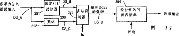
Not so, according to design of the present invention, two channels also can adopt a kind of method that is called two Stage interpolation.Can improve the frequency response of adjustable interpolation filter with this two step method, this method just is referred to as two Stage interpolation device system after in this manual.Two Stage interpolation device of the present invention comprises fixing finite impulse response (FIR) filter and the variable interpolater of four-point of coefficient with (2n+4) individual tap.The output of FIR filter is placed in going up between all input pixel samplings midway.Output ginseng with the FIR filter is inserted in the former data sampling then, former data sampling is postponed, thereby produce an efficient sampling rate 2fs.All frequencies in the FIR filter passband, can suppose so fully.The result who does like this is the effective passband that has enlarged former 4 interpolaters greatly.
As long as the frequency component of signal is not more than the about 1/4th of sampling rate, i.e. 0.25fs, then the compensate for variable interpolation filter of prior art is what can accurately provide through the sampling of interpolation.Described two step method can be used for frequency component basically greater than the signal of 0.25fs.According to design of the present invention, be the secondary signal of representing the signaling point digital sampling between each sampling of first signal with a finite impulse response filter from first signal generation of digital sampling.First signal is for example to flow determined vision signal by pixel value data.First signal system process postpones, but in others not change basically.Secondary signal and the first delayed signal are to interlock with for example multiplexer, and to produce the 3rd signal of digital value, the sampling density that has is the twice of first signal.Variable interpolater through compensation draws the 4th signal of digital sampling from the 3rd signal, and wherein the frequency content of the represented information of first signal changes.This frequency content is compressed or expands.The frequency component of first signal can be unlikely to significantly to reduce the bandwidth of the 4th signal up to the first sample of signal rate about 40%, even also be like this when expansion.When amplifying by represented visual of vision signal, vision signal postponed by finite impulse response filter and handle before can be in FIFO line storage for example in addition brachymemma.For selected compression or ratio are provided, can control this adjustable interpolater with for example microprocessor or hardware device through compensation.
The objective of the invention is to improve the frequency component of the video information of the signal that in having band-limited finite impulse response, produces.In order to realize the present invention, comprise the finite impulse response filter of the secondary signal of the digital sampling of signaling point between each sampling that has certain bandwidth and from first signal of the digital sampling of representing video information, produce expression first signal according to interpolation system provided by the present invention; Be used for the device of described first signal delay and be used for the secondary signal and delayed first signal are interlocked to produce the device of its sampling density greater than the 3rd signal of the digital value of first signal.This system also comprises the variable interpolater through compensation, be used for obtaining from the 3rd signal the 4th signal of digital sampling, this variable interpolater increases certain bandwidth of filter and thereby improves frequency content with respect to video information in the 4th signal of the video information of representing original signal in first signal.
Fig. 1 (a)-1 (i) is in order to the different display format of explanation panavision.
Fig. 2 is various aspects and the suitable block diagram that carries out the panavision of horizontal sweep work by 2f according to the present invention.
Fig. 3 is the block diagram of wide-screen processor shown in Figure 2.
The block diagram of Fig. 4 shows the more detailed details of wide-screen processor shown in Figure 3.
Fig. 5 is the block diagram of picture-in-picture processor shown in Figure 4.
Fig. 6 is the block diagram of gate array shown in Figure 4, shows main signal path, auxiliary signal path and output signal path.
Fig. 7 and 8 helps the timing diagram with the process of the display format of picture very restricted signal generation of explanation as Fig. 1 (d) shown in.
The block diagram of Fig. 9 shows the main signal path of Fig. 6 more detailedly.
The block diagram of Figure 10 illustrates in greater detail the auxiliary signal path of Fig. 6.
Figure 11 is the block diagram of timing of Fig. 5 picture-in-picture processor and control section.
Figure 12 produces 1f
H-2f
HInterior 2f in the conversion
HThe block diagram of the circuit of signal.
Figure 13 is the frame circuit diagram of deflection circuit shown in Figure 2.
Figure 14 is the block diagram of rgb interface shown in Figure 2.
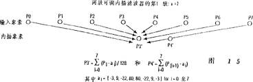
Figure 15 and 16 is the pixel patterns that can be used as the adjustable interpolation filter working condition of two-stage of Fig. 6, each interpolater of 9 and 10 in order to explanation.
Figure 17 is the block diagram of two-stage through the variable interpolation filter of compensation.
Figure 18 is the block diagram for the variable interpolation filter of two-stage through compensating of realizing the zoom feature body plan.
Figure 19 is the block diagram as the circuit of eight tap two Stage interpolation filters.
The each several part of Fig. 1 shows can be by single and some of a plurality of visual display formats rather than whole various composite types of various different designs enforcements of the present invention.Here selected all is the example of enumerating for ease of explanation constitutes the particular electrical circuit of panavision by design of the present invention.Design of the present invention relates to display format in some cases and compares itself except that relating to concrete basic circuit.For the purpose of explanation and discussing, traditional display format the ratio of width to height of video source or signal is assumed to be 4 * 3 usually, and wide screen display format the ratio of width to height of video source or signal then is assumed to be 16 * 9 usually.Each design of the present invention is not subjected to these predetermined restricted.
It is 4 * 3 directly perceived or projection TV that Fig. 1 (a) shows general display format ratio.When 16 * 9 display formats transmitted than signal as 4 * 3 display formats than image, blackstreak appearred in the top of screen and bottom, and this is commonly called letterbox format (letterboxformat).At this moment the image of being seen is smaller than whole available viewing area.Not so, also can be before transmission with the in addition conversion of the signal source of 16 * 9 display formats ratio, thereby make it be full of the vertical direction of 4 * 3 display format pictures.But so just have many information may from the left side and or the right picture be limited.Select as another kind, the image of mailbox formula can be expanded in vertical direction, but do not expanded in the horizontal direction, the image that draws like this will be because of the vertical extent distortion.These three kinds of ways all do not have special saving grace.
Fig. 1 (b) shows 16 * 9 screen.The video source of 16 * 9 display formats ratio can show comprehensively, and picture is not only unrestricted but also undistorted.The mailbox formula image of 16 * 9 display formats ratio itself is in the signal of 4 * 3 display formats ratio, and this image can be lined by line scan by row is added to be twice or to add capable method, thereby provides showing than large format of enough vertical definitions.No matter signal source is master source, auxiliary source or outside rgb signal source, and panavision of the present invention can both show the signal of this 16 * 9 display formats ratio.
Fig. 1 (c) shows the main signal of 16 * 9 display formats ratio, and the illustration of 4 * 3 display formats ratio promptly shows in this signal.If main video signal and auxiliary video signal all be 16 * 9 display formats than signal source, then the display format of illustration is than also being 16 * 9.Illustration can be presented at many diverse locations.
Main video signal and auxiliary video signal all use the image with size to show in the display format that Fig. 1 (d) illustrates.The display format of each viewing area is 8 * 9 than all, this certainly with 16 * 9 and 4 * 3 display format than different.Be to show the unlikely generation level of signal source or the vertical distortion of 4 * 3 display formats ratio in such viewing area, signal inevitable in the left side and/or the right side be subjected to the restriction of picture.If allow the ratio of width to height, then can demonstrate more, the less image of its picture limited degree because image is squeezed and some distortion in the horizontal direction.The level extruding makes the vertical elongated in kind in the image.Panavision of the present invention can provide " picture is restricted " and " the ratio of width to height distortion " these two any combined situation in following combination range, that is, one of this scope extremely is: maximum " picture is restricted " and nothing " the ratio of width to height distortion " combined situation; Another extremely is: do not have " picture is restricted " and maximum " the ratio of width to height distortion " combined situation.
Auxiliary video signal is handled all restrictions of in the path data being taken a sample, and the feasible displayed image that produces has high definition and visual breadth is complicated with the same big whole signal processing of displayed image that main video signal produces.Solve these complicated problems various method can be arranged.
The display format of Fig. 1 (e) is the image that demonstrates 14 * 3 display formats ratio at the screen position placed in the middle of 16 * 9 display formats ratio.The secret note in right side and left side clearly.
The display format that Fig. 1 (f) illustrates demonstrates the big image of one 4 * 3 display format ratio and the less image of three 4 * 3 display format ratios simultaneously.Outside big image periphery, there is the display format of less image to be called POP sometimes, i.e. picture out picture, rather than PIP (picture-in-picture).Here, two kinds of display formats all adopt PIP or picture-in-picture one speech.Be provided with the occasion of two tuners at panavision, two tuners all are located at an other places configuration (for example in the video cassette recorder) in inside or, just can make two images in each displayed image demonstrate the real-time action consistent with signal source, remaining image can show with the form that freezes frame.Be understood that, set up other tuner and other auxiliary signal and handle path plural active images can be provided.Should be understood that also that the position of big image and three little images can be exchanged, shown in Fig. 1 (g).
The another kind of display format that Fig. 1 (h) illustrates is: the image of one 4 * 3 display format ratio is in the centre, line up file 64 * 3 display format ratios less image each on both sides.The same with above-mentioned form, there is the panavision of two tuners that the image of two activities can be provided.Remaining 11 image just shows with the form that freezes frame.
Fig. 1 (i) shows the display format of the grid of being made up of 12 4 * 3 display format ratio images.This display format is particularly suitable as the channel selection guide, and wherein each image is freezing frame of a different channel at least.As before, the number of active images depends on the number of spendable tuner and signal processing path.
Various different-formats shown in Figure 1 just illustrate, and are not limited to these, and these forms can be by being implemented with the following panavision that is about to introduce in detail shown in following each accompanying drawing.
It is suitable to 2f that Fig. 2 shows the present invention
HThe block diagram of the panavision of horizontal sweep mode work, its master serial number are 10.Panavision 10 generally includes video signal input section 20, chassis or TV microprocessor 216, widescreen processor 30,1f
H-2f
HTransducer 40, deflection circuit 50, rgb interface 60, YUV-RGB transducer 240, picture tube driver 242, directly perceived or projection kinescope 244 and power supply 70.Various circuit are grouped into different function square frames do like this, do not wish therefore to have limited these circuit actual disposition position each other for the ease of describing.
Video signal input section 20 is in order to receive a plurality of composite video signals from the different video source.Each vision signal can be switched selectively, is that main video signal and auxiliary video signal show that radio-frequency (RF) switch 204 has two antenna input ANT1 and ANT2 so that it is turned into.These are respectively the inputs that receives the signal of the signal of broadcast antenna and cable.Radio-frequency (RF) switch 204 controls wherein which input are provided to first tuner 206 and second tuner 208.The output of first tuner 206 is the input of single-chip 202, and single-chip 202 is fulfiled and tuning, level and vertical deflection and the relevant a series of functions of video control.Certain chip shown in the figure is called the 7A7777 cake core in the electronics industry industry.Cause supplies with in the baseband video signal VIDEO OUT output back that produces from the signal of first tuner 206 input of presentation switch 200 and widescreen processor 30TVI in the single-chip.Other is to the base band video input called after AUX1 and the AUX2 of video switch 200.Their uses such as looking video camera, disc player, video player, electronic game machine of can powering.The output of video switch 200 is by chassis or TV microprocessor 216 controls, called after SWITCHED VIDEO (video of switching).SWITCHEDVIDEO is another input of widescreen processor 30.
Referring again to Fig. 3.Switch SW 1 widescreen processor selects one of TV1 and these two signals of SWITCHED VIDEO as SEL COMP OUT vision signal, and this is an input signal of Y/C decoder 210.Y/C decoder 210 can be a self adaptation row comb filter.In addition two video source S1 and S2 also are the inputs of Y/C decoder 210.S1 respectively represents different S-VHS sources with S2, and they respectively are made up of luminance signal of separating and carrier chrominance signal.A part (as in the situation of some self adaptation row comb filter) that can be used as the Y/C decoder is arranged or as the switch of discrete switch, it in response to TV microprocessor 216 so that choose a pair of luminance and chrominance information as the output of called after Y_M and C_IN respectively.Selected a pair of brightness and luminance signal are later just as main signal, and handle along main signal path choosing row.Include in the signal name _ M or _ signal name of MN refers to main signal path.Widescreen processor draws the receipt chip again to luminance signal C_IN, so that produce color difference signal U_M and V_M.Here, U is equivalent to (R-Y), and V is equivalent to (B-Y).Y_M, U_M and V_M signal are converted into digital form so that further carry out signal processing in widescreen processor.
Second tuner 208 belongs to the part of widescreen processor 30 on function, it produces baseband video signal TV2.Switch SW 2 is from selecting the input of a signal as Y/C decoder 220 between TV2 and two signals of SWITCHED VIDEO.Y/C decoder 220 can be a self adaptation row comb filter.Switch SW 3 and SW4 respectively from the brightness of Y/C decoder 220 and colourity output with also select signal between the luminance and chrominance information of called after Y_EXT and C_EXT respectively from outer eikongen.Y_EXT and C_EXT signal are imported S1 corresponding to S_VHS.Y/C decoder 220 can be as combining at some auto-adaptive comb filter with SW4 with switch SW 3.Just the output of switch SW 3 and SW4 is handled as auxiliary signal and along the auxiliary signal path later.Selected brightness output called after Y_A.Indicate _ A, _ AX and _ the AUX signal name refer to the auxiliary signal path.Selected colourity output is converted into color difference signal U_A and V_A.Y_A, U_A and V_A signal are converted into digital form so that further carry out signal processing.On main signal and auxiliary signal path, make the management process that the signal source of each different piece of different visual display formats is selected reach maximum flexibility to the switched design of video signal source.
Widescreen processor provides composite synchronizing signal COMP SYNC corresponding to Y_M for sync separator 212.Level and vertical synchronization component H and the V input of the vertical countdown circuit 214 of conduct respectively.Vertical countdown circuit produces VERTICAL RESET (vertical reset) signal and is added in the widescreen processor 30.Vertical reset output signal INT VERTRST OUT was added to rgb interface 60 in widescreen processor produced.A switch in the rgb interface from interior vertical reset output signal and outside choose signal between the vertical synchronization component in RGB source.The output of this switch is the vertical synchronization component SEL_VERT_SYNC through selecting that guides to deflection circuit 50.The level of auxiliary video signal and vertical synchronizing signal are produced by the sync separator in the widescreen processor 250.
1f
H-2f
HTransducer 40 is in order to converting interlaced video signal to the non-interlaced scan signals of lining by line scan, for example the sort of each horizontal line show twice or by interpolation with adjoin the signal that horizontal line produces another group horizontal line.In some cases, use lastrow or use interpolation line to depend on and adjoining detected action degree (the level of movement) between each or each frame.Change-over circuit 40 and video-ram 420 associated working.Video-ram can be in order to store one or more fields of a frame, so that can show one by one.Video data through changing is as Y_2f
H, U_2f
HAnd V_2f
HBe added on the rgb interface 60.
The rgb interface that illustrates in greater detail in Figure 15 60 makes and video data or outer rgb video data through conversion can be chosen for video signal input section so that for showing usefulness.Outer rgb signal can be considered suitable wide display format for 2f scanning and compares signal.Widescreen processor is fed to rgb interface with the vertical synchronization component of main signal as INT VERT RST OUT, makes deflection circuit 50 can obtain vertical synchronizing signal (fvm or fv through choosing
Ext).During panavision work, the TV user just can choose outer rgb signal by producing inside/outside control signal INT/EXT.But the rgb signal input time can make grating disappear in vertical direction and damages cathode ray tube or projection kinescope outside choosing under not having the situation of outer rgb signal.Therefore choose outer RGB import under this RST not for unlikely, the rgb interface circuit detects external synchronization signal.WSP microprocessor 340 is also controlled the colour and the tone of outer rgb signal.
Deflection circuit 50 (this shows more in detail in Figure 14) receives vertical reset signal from widescreen processor, from the 2f horizontal-drive signal through selecting of rgb interface 60 with from other control signals of widescreen processor.These additional control signals are relevant with horizontal phasing, vertical dimension adjustment and Dong-Xi pincushion distortion adjustment (east-west pinadjustment).Deflection circuit 50 is with 2f
HFlyback pulse is fed to widescreen processor 30,1f
H-2f
HOn transducer 40 and the YUV-RGB transducer 240.
Power supply 70 produces the operating voltage of whole panavision by the electric main power supply.
Fig. 3 illustrates in greater detail widescreen processor 30.The critical piece of widescreen processor has gate array 300, picture-in-picture circuit 301, mould-number and D-A converter, second tuner 208, widescreen processor microprocessor 340 and widescreen output coder 227.Fig. 4 shows the more detailed details of widescreen processor (for example PIP circuit), and this is to 1f
HAnd 2f
HThe chassis is common.Fig. 5 illustrates in greater detail the picture-in-picture processor 320 that constitutes PIP circuit 301 major parts.Fig. 6 illustrates in greater detail gate array 300.Formation main signal path shown in Figure 3 and auxiliary signal were introduced in detail by a series of parts of each several part.
Second tuner 208 is connected with intermediater-frequency stage 224 and audio frequency stage 226.Second tuner 208 also with WSP μ P340 associated working.WSP μ P340 comprises input and output I/O part 340A and simulation output 340B.I/O part 340A provides the color harmony color control signal, select the INT/EXT signal that outer rgb video source uses and the control signal of switch SW 1 to SW6.The I/O part is also monitored the EXT SYNC DET signal from rgb interface, thus protection deflection circuit and cathode ray tube.Simulation output 340B provides the control signal of vertical dimension, thing adjustment and horizontal phase by each interface circuit 254,256 and 258.
Color component signal represents with generic name U and V, these signals or can distribute to R-Y or B-Y signal or can distribute to I and Q signal.The brightness bandwidth constraints of being taken a sample is at 8 megahertzes, and this is because the clock pulse frequency of system is 1024f
H, this is approximately 16 megahertzes.Since width when being I U and V signal system be limited in 500 kilo hertzs or 1.5 megahertzes, so can adopt single analog-digital converter and an analog switch when color component data taken a sample.The selection wire UV_MUX of analog switch or multiplexer 344 is divided by the 28 megahertz signals that obtain with system clock pulse.Capable starting impulse SOL with a clock signal width synchronously makes this signal reset to 0 when each horizontal video line begins.Its state so UV_MUX line each clock cycle in whole horizontal line overturns.Equal even number clock cycle because row is long, thereby the state of UV_MUX does not overturn all the time interruptedly once the startup meeting.0,1,0,1 ...,, thereby all be shifted from Y and the UV data flow that analog- digital converter 342 and 346 comes out because each analog-digital converter all has the time delay of 1 clock cycle.For adapting to this data shift, handle from main signal that gated information also must similarly postpone in the clock arteries and veins of interpolater controller 349 of path 304.Gated information postpones in the clock arteries and veins if do not make, and the UV data just can not be correctly paired when deleted.This point is very important, because each UV is to representing a vector.With the U component of a vector and the pairing of another vectorial V component and do not cause that colour shift is impossible.On the contrary, going up a pair of V sampling can be deleted simultaneously together with existing U sampling.Because (U, V) sampling has two brightness samplings to every pair of chrominance component, so the method for this UV multichannel modulation is called 2: 1: 1 modulation methods.At this moment just make the Nai Kuisi frequency of U and V be reduced to half that brightness Nai Kuisi holds frequency effectively.Therefore the Nai Kuisi frequency of exporting for the analog-digital converter of luminance component is 8 megahertzes, and the Nai Kuisi frequency of exporting for the analog-digital converter of chrominance component is 4 megahertzes.
Although PIP circuit and/or gate array also can comprise data and also can improve the device of auxiliary data definition by compression.Worked out a series of data reductions and data recovery scheme so far, for example comprised that pixel compresses and shivers tuning (dithering) and go to shiver tuning (dedithering) in pairs.The different pixels in pairs that the difference of considering to relate to different number of bits is in addition shivered tuning sequence and related to different number of bits compress.WSP μ P340 can choose a scheme in reduction of a series of particular datas and the recovery scheme so that make the shown image of visual display format of each particular types reach the highest definition.
Gate array comprises some interpolaters with each line storage associated working, and each line storage then can be FIFO356 and 358.Interpolater and FIFO are in order to take a sample to main signal where necessary again.An additional interpolater can be taken a sample to auxiliary signal again.The data management processes of the clock pulse in the gate array and synchronous circuit control main signal and auxiliary signal comprises they is formed the single outputting video signal with Y_MX, U_MX and V_MX component.These output components convert analog form to by D-A converter 360,362 and 364.The signal of the analog form of called after Y, U and V is added to 1f
H-2f
HOn the transducer 40 so that convert the non-interlace mode to.Y, U and V signal also are encoded into the Y/C form to be formed on the retrievable wide format specific output signal Y_OUT_EXT/C_OUT-EXT of panel jack place by encoder 227.Switch SW 5 selects synchronizing signal C_SYNC-MN from gate array for encoder 227, or selects synchronizing signal C SYNC-AUX from the PIP circuit.Switch SW 6 is selected the synchronizing signal of signal as the wide-screen panel output from Y_M and C_SYNC_AUX between the two.
Figure 12 illustrates in greater detail the each several part of horizontal-synchronizing circuit.Phase comparator 228 is parts of a phase-locked loop, and this phase-locked loop also comprises low pass filter 230, voltage controlled oscillator 232, divider 234 and capacitor 236.Voltage controlled oscillator 232 response ceramic resonators (or and so on) 238, at 32f
HFollowing work.The output of voltage controlled oscillator is divided by 32, so that provide the second suitable input signal of frequency for phase comparator 228.The output of divider 234 is 1f
HThe REF timing signal.32f
HREF and 1f
HBoth are added to the REF timing signal except that on 16 counters 400.2f output is fed on the pulse width circuit 402.Use 1f
HThe REF signal presets divider 400, can guarantee that like this divider synchronouss working with the phase-locked loop of picture intelligence importation.Width circuit 402 is guaranteed the correct work of pulse duration sufficient to guarantee phase comparator 404 (for example CA1391 type phase comparator) of 2f-REF signal in the arteries and veins, phase comparator 404 forms the part of second phase-locked loop, and second phase-locked loop then comprises low pass filter 406 and 2f
HVoltage controlled oscillator 408.Voltage controlled oscillator 408 produces 2f
HInterior timing signal, the demonstration of lining by line scan is promptly driven by this signal.Another input signal that is added to phase comparator 404 is 2f
HFlyback pulse or the timing signal relevant with flyback pulse.Employing comprises that second phase-locked loop of phase comparator 404 helps to guarantee 2f
HScan period is at each 1f of input signal
HPeriodic symmetry.If not, grating division phenomenon can appear in the picture that shows, and for example, the image row has half to move on to the right side, has half to move on to the left side.
Figure 13 illustrates in greater detail deflection circuit 50.The vertical dimension of circuit 500 in order to regulate grating according to the needed vertically passing scanning amount that meets the requirements of the different display format of realization.Shown in schematic diagram, constant-current source 502 provides the electric current I of constant
RAMPGive the vertical ramp capacitor 504 chargings.Transistor 506 is connected in parallel with the vertical ramp capacitor, periodically gives this capacitor discharge according to vertical reset signal.Do not carrying out under the situation of any adjusting electric current I
RAMPMake the vertical dimension of grating reach the maximum that can reach.This may be equivalent to needed vertically passing scanning amount when 4 * 3 display formats of an expansion are full of wide screen displays (as shown in Fig. 1 a) than signal source.Require under the less situation in the grating vertical dimension, adjustable current source 508 is from I
RAMPShift the transformable electric current I of its magnitude of current
ADJThereby, make vertical ramp capacitor 504 with the charging of slower speed and charge to than small leak.Variable current source 508 response vertical dimension control circuits are produced for example is the vertical dimension conditioning signal of analog form.Vertical dimension regulating circuit 500 is with manually vertical dimension regulating circuit 510 is irrelevant, and the latter can be a potentiometer or backplate adjusting knob.Under above-mentioned any situation among both, frame deflector coil 512 all receive an amount of drive current in case with image transform to display.Horizontal deflection signal is by phase modulation circuit 518, Dong-Xi pillow distortion equalizing circuit 514,2f
HPhase-locked loop 520 and horizontal output circuit 516 provide.
Figure 14 illustrates in greater detail rgb interface circuit 60.The signal that will show is at 1f at last
H-2f
HThe output of transducer 40 is selected between the two with the input of outer RGB, and the input hypothesis of its outer RGB of panavision described here is the progressive-source that wide format shows ratio.Outer rgb signal and composite blanking signal from video signal input section 20 are input in the RGB-YUV transducer 610.The outer 2f of outer rgb signal
HComposite synchronizing signal is used as the input of external synchronization signal separator 600.Selecting vertical synchronizing signal is to be carried out by switch 608.Selecting horizontal-drive signal is to be carried out by switch 604.Selecting vision signal is to be carried out by switch 606.The inside/outside control signal that each switch 604,606 and 608 response WSP μ P340 are produced.Selection interior or outer video source is undertaken by the user.But if the user selects outer RGB source unintentionally, if when not being connected to or during access failure sort signal source or external signal source when losing, then vertical raster can disappear, so can cause serious damage to cathode ray tube.Therefore outer synchronizing indicator 602 detects not external synchronization signal existence.When not having sort signal, just there is a switch refusal control signal to be sent on each switch 604,606 and 608, in case when not having signal, pass through RGB source outside these switches selections.RGB-YUV transducer 610 also receives the color harmony color control signal from WSP μ P340.
Panavision of the present invention can be without 2f
HHorizontal sweep and use 1f
HHorizontal sweep is implemented, but 1f is not shown here
HThe circuit of horizontal sweep.1f
HCircuit may not need 1f
H-2f
HTransducer and rgb interface.Therefore not at 2f
HShow under the scanning frequency that outside wide format shows the measure than rgb signal.Widescreen processor and 1f
HThe picture-in-picture processor of circuit is extremely similar.Gate array is substantially the same, but whole inputs and output is not all used.No matter be with 1f
HScanning or with 2f
HThe TV of scan mode work, the various schemes that promote clearness described here all are suitable for usually.
The details of the widescreen processor 30 shown in Fig. 3 that the block diagram of Fig. 4 illustrates in greater detail, it is to 1f
HAnd 2f
HThe chassis all is identical.Y_A, U_A and V_A signal are an input of picture-in-picture processor 320, and processor 320 can comprise definition treatment circuit 370, and the panavision of these aspects can be expanded video and compress according to the present invention.The special-effect that the combined type display format shown in the part is embodied among Fig. 1 is produced by picture-in-picture processor 320, this processor can receive data-signal Y_RP, U_RP and the V_RP through the definition processing from definition treatment circuit 370, be not whenever all to use definition to handle, but when display format is chosen, will use.Fig. 5 illustrates in greater detail picture-in-picture processor 320.The critical piece of picture-in-picture processor has analog-to-digital conversion part 322, importation 324, high-speed switch (FSW) and bus portion 326, timing and control section 328 and number-Mo conversion portion 330.Illustrate in greater detail timing and control section 328 among Fig. 9.
The modification that picture-in-picture processor 320 can adopt the Thomson consumer electronics company in the Indianapolis city of Indiana, USA to develop through improved basic CPIP chip.More fully introduced the situation of CPIP chip in " CTC 140 picture-in-picture techniques training manuals " that the said firm goes out.Sort processor can make it have a series of special features or special effect, and explanation below gives some instances.Basic special-effect is that the sort of part at big image as shown in Fig. 1 (c) is overlapping a little image.The size image can be from same video signal generating, from different video signal generating, but also can exchange or change.In general, audio signal always switches to and makes it corresponding to big image.Little image can move on to any position on the screen or phase out into a series of precalculated positions.The variable characteristics of focal length make and can and narrow down to for example arbitrary predetermined size with little image multiplication.Sometimes, for example in the display format shown in Fig. 1 (d), big or small image is actually same size.
Under free hand drawing resembled show state, for example under the show state shown in Fig. 1 (b), 1 (e) or 1 (f), the user can be for example progressively amplifies by the zoom mode from 1.0: 1 to 5.0: 1 the ratio picture with the free hand drawing elephant.Simultaneously when the zoom mode, user's whole image of can searching for or pan makes video on the panel be striden different area of images and moves.Under both situations, no matter be that little image, big image or zoom image can show in the mode (still image form) of freezing frame.This function can realize the gating display format, and at this moment last nine frames in the vision signal can show on screen repeatedly.The repetition rate of frame can change to for 0 frame/second from 30 frame/seconds.
Employed picture-in-picture processor is different with the existing structure of above-mentioned basic CPIP chip itself in the panavision of the another kind of design of the present invention.As if the TV adapted of basic CPIP chip and 16 * 9 screens and without video speedup circuit, then reach 4/3 times to expansion, thereby make illustration present the phenomenon of the ratio of width to height distortion owing to 16 * 9 screen scannings that traverse broad cause real standard.So the material object in the image may horizontal extension.If adopt outer speedup circuit, then do not have the ratio of width to height distortion, but image can account for discontented whole screen.
The existing picture-in-picture processor of mainly being made up of basic CPIP chip that is adopted in the traditional tv is to move having under the ad hoc fashion of some undesirable consequence.The video that input comes is taken a sample with the 640f clock pulse of the horizontal-drive signal that locks onto main video source.In other words, the data that are stored in the video-ram relevant with the CPIP chip are not the auxiliary video source quadrature-sampleds that comes with respect to input.This is the basic limitation of the basic CPIP method of field synchronization.The nonopiate character of this of input sampling rate makes in the data of being taken a sample and produces non-symmetric error.Above-mentioned limitation is to be caused by the video-ram with CPIP chip adapted, and this memory must use same clock pulse read and write data.When showing from video-ram, during the data of (for example video-ram 350), the form that asymmetric error just moves with irregular instability on the vertical edge of image occurs, and is considered to usually be a problem very much.
The picture-in-picture processor 320 of the another kind design that the present invention is different with basic CPIP chip is suitable to the asymmetric a kind of state that is compressed in the multiple show state of video data.Under this operating state, each image ties up on the horizontal direction by compression in 4: 1, in vertical direction by compression in 3: 1.The working method of this asymmetric compression produces the image of width height ratio distortion, is used for being stored in a video-ram.Each material object seems to be squeezed as horizontal direction in the image.But if these data are read by normal mode, for example read in the channel scanning mode so that be presented at 16 * 9 display formats than on the screen, then the object in the image seems normal.Image is full of screen, and does not have the image aspect distortion phenomenon.Making according to the asymmetric compress mode of this respect of the present invention can outer speedup circuit and can produce special display format on 16 * 9 screen.
Figure 11 be picture-in-picture processor (for example above-mentioned CPIP chip is through an improved kind) fixed to the block diagram of control section 328, this part comprises gets several parts of circuit 328C in ten parts, in order to carry out the asymmetric compression as a mode in a plurality of selectable display modes.Remaining display mode can provide the auxiliary image of different sizes.Each level with vertical ten parts in get several parts of circuit have one under WSP μ P340 control according to the counter of a numerical tabular by a certain bulkfactor programming.This numerical value can be 1: 1,2: 1,3: 1 etc. scope, and bulkfactor can be a symmetry or asymmetric, and this depends on this numerical tabular how to work out and decide.The control of compression ratio also can be under the control of WSP μ P340 be undertaken by get several parts of circuit in ten parts of the general services that can programme comprehensively.
Under full screen PIP state, picture-in-picture processor combines with self-excited oscillator (freerunning oscillator) 348, to get the Y/C input from a decoder (for example self adaptation row comb filter), signal decoding is become Y, U, V color component, and generation level and vertical sync pulse.These signals are being used for such as zoom, are freezing frame and the picture-in-picture processor of various full screen display modes such as channel scanning is handled.For example, during the channel scanning display mode, because sampled signal (different channel) has incoherent lock-out pulse and can not consider that each letter is at random constantly being switched, so sampling clock pulse (with read/write video-ram clock pulse) is determined by self-excited oscillator 348.Display mode is for freezing frame and during the zoom mode, sampling clock pulse can lock onto on the horizontal synchronization pulse of input video, and at these in particular cases, this is identical with the read clock pulse frequency.
Referring again to Fig. 4, can be encoded into the Y/C component again from picture-in-picture processor by coding circuit 366 with Y, U, V and C_SYNC (composite sync) output that analog form occurs, coding circuit 366 is with 380 associated working of 3.58 megahertz oscillator.This Y/C_PIP_ENC signal can be received Y/C switch (not shown), and this switch makes the Y/C component behind the coding can replace the Y/C component of main signal again.From this time, Y, U, V and the synchronizing signal through the PIP coding become the level and vertical basis regularly of remainder in the chassis.The suitable zoom display mode of implementing PIP according to the working condition of interpolater in the main signal path and FIFO of this working method.
Referring again to Fig. 5.Picture-in-picture processor 320 comprises analog-to-digital conversion part 322, importation 324, high-speed switch FSW and bus control section 326, timing and control section 328 and number-Mo conversion portion 330.Usually, picture-in-picture processor 320 becomes brightness (Y) and color difference signal with video signal digitization (U V), carries out secondary sample with the gained result and is stored in the video-ram 350 of 1 megabit, as described above.Video-ram 350 its memory capacity relevant with picture-in-picture processor 320 are its off-capacity of 1 megabit with whole of the video data of 8 binary digits samplings of file.The capacity that increases storage must spend greatly, and needs more complicated management circuit.The figure place that reduces per unit sampling in the auxiliary channel means quantification definition or the bandwidth of minimizing with respect to main signal, and this main signal is handled by 8 samplings all the time.Actual this bandwidth reduce when auxiliary displayed image hour normally unchallenged, but when if auxiliary displayed image is big, during for example with the general size of main displayed image, existing problems just.Definition treatment circuit 370 can implement to improve one or more schemes of auxiliary video data-measuring definition or effective bandwidth selectively.Worked out the scheme that a series of reduction data and data are recovered so far, for example comprised pixel compression in pairs and shiver tuning and go the tuning scheme of shivering.Make the tuning circuit that goes to shiver when work, be configured in video-ram 350 downstream parts, for example in the auxiliary signal path of gate array, be about to below introduce in more detail.It is also conceivable that in addition relate to the difference of isotopic number not shiver tuning and go to shiver tuning sequence with relate to the not different pixel compression schemes in pairs of isotopic number.For the image that each extraordinary visual display format is shown reaches the highest definition, can from the scheme of a series of minimizings and restore data, choose a kind of scheme by WSP μ P.
YUV is stored by 8.1: 1 six Y, U, V mode.In other words, each element quantization is become six samplings.Every pair of aberration sampling has eight brightness samplings.Picture-in-picture processor 320 changes in such a way works, and wherein Shu Ru video data is the 640f with the auxiliary video synchronizing signal that locks onto input
HClock frequency is taken a sample.Under this working method, be stored in data in the video-ram and be quadrature-sampled.During from picture-in-picture processor video-ram 350 sense datas, also must utilize the same 640f on the auxiliary video signal that locks onto input
HClock pulse and read these data to keep orthogonality relation.Though but these data are quadrature-sampleds and store, and can read orthogonally,, make these data can not directly from video-ram 350, be used for quadrature and show because the asynchronous character of main video and auxiliary video source.It is synchronous that main video and auxiliary video source only just can be look to when they are shows signal from same video source.
In order to make the auxiliary channel dateout of video-ram 350 (promptly from) and main channel synchronous, need further handle.Referring again to Fig. 4, reconfigured with two four latch 352A and 352B from 8 bit data block of 4 output ports of video-ram.These four latchs also make data clock arteries and veins medium frequency from 1280f
HDrop to 640f
H
Normally make video demonstration and deflection system and main video signal synchronous.As mentioned above, must quicken so that it is full of widescreen display main video signal.Must make the auxiliary video signal and first vision signal and video display vertical synchronization.But postpone a part field duration in the auxiliary video signal field memories, in line storage, expanded then.The synchronization utilization of auxiliary video data and main video data realizes as the video-ram 350 of field memory with in order to first in first out (FIFO) line storage 354 of spread signal.The specification of FIFO354 is 2048 * 8.The specification of FIFO with think for avoiding the read/write pointer necessary capable minimum memory size that conflicts relevant.Read/write pointer clashed before new data has an opportunity to write FIFO and takes place when FIFO reads legacy data.Read/write pointer clashes also and can have an opportunity to take place when new data is rewritten memory before FIFO reads at legacy data.
From 8 DATA_PIP data blocks of video-ram 350 are 640f with the same picture-in-picture processor that once was used for video data is taken a sample
HClock pulse (promptly locks onto the 640f on auxiliary signal rather than the main signal
HClock pulse) writes among 2048 * 8 FIFO354.FIFO354 uses 1024f
HThe read clock pulse read, this clock pulse system locks onto on the horizontal synchronization component of main video channel.Owing to adopt the multirow memory (FIFO) that has in the independent read/write port clock arteries and veins, thereby allow the general once to show with the second speed quadrature with the data of first rate quadrature-sampled.But because the read/write clock pulse has asynchronous character, thereby need to take various steps to avoid read/write pointer to clash really.
Show main signal path 304, auxiliary signal path 306 and the output signal path 312 of gate array 300 among Fig. 6 with the form of block diagram.Gate array also comprises clock pulse/synchronous circuit 320 ' and WSP μ P decoder 31O.The data of WSP μ P decoder 310 and address outlet line (representing with WSP DATA) are to be added on above-mentioned each main circuit and the path, and are added on picture-in-picture processor 320 and the definition treatment circuit 370.It should be understood that whether some circuit is set to is the part of gate array, only is for ease of design of the present invention is described to a great extent.
Gate array is in order to the video data of expanding, compress main video channel where necessary and limits its picture, so that realize different visual display formats.Luminance component Y_MN is stored in first in first out (FIFO) line storage 356, and the length of memory time depends on the character of luminance component interpolation.Chromatic component U/V-MN through combination is stored among the FIFO358.Auxiliary signal brightness and chromatic component Y_PIP, U_PIP and V_PIP are produced by demultiplexer 355.Luminance component is handled through definition in circuit 357 in case of necessity, is expanded by interpolater 359 in case of necessity then, produces the signal Y_AUX as output.
In some cases, the auxiliary demonstration can be generally big with the main signal demonstration, shown in the example among Fig. 1 (d).The memory limitations relevant with picture-in-picture processor and video-ram 350 can make and be full of needed data point in this large-scale viewing area or pixel number deficiency.In this case, can pixel be reverted to the pixel to replace those to lose in the auxiliary video signal in data compression or reduction process with definition treatment circuit 357.This clear degree is handled and can be handled corresponding to the definition that circuit shown in Figure 4 370 is carried out.For example, circuit 370 can be the tuning circuit of shivering, and circuit 357 can be the tuning circuit of shivering.
Auxiliary video input data tie up to 640f
HSampling sampling down deposits in the video-ram 350 then.The auxiliary data called after VRAM OUT that reads from video-ram.PIP circuit 301 can also dwindle auxiliary image with the integer factors that equates in the horizontal and vertical directions, also can asymmetric diminished image.Referring again to Fig. 1 O, can see that the auxiliary channel data are cushioned and make itself and main channel digital video synchronous by 4 latch 352A and 352B, auxiliary FIFO354, timing circuit 369 and synchronous circuit 368.VRAM OUT data are categorized as Y (brightness), U, V (chromatic component) and FSW_DAT (high-speed switch data) by demultiplexer 355.FSW_DAT shows that being written in the video-ram is any field pattern.PIP_FSW directly receives from the PIP circuit and is added to the output of control circuit 321 then to determine should to show that field of reading from video-ram under little visual display mode.
Auxiliary channel is with 640f
HSample at rates, main channel is then with 1024f
HSample at rates.Auxiliary channel FIFO354 becomes the main channel clock frequency with data from the auxiliary channel sample rate conversion.In this process, vision signal compression of (promptly 1024/640) through 8/5.This correct demonstration auxiliary channel signal required 4/3 the compression more than.Therefore auxiliary channel must be expanded so that correctly show 4 * 3 little image by means of interpolater 359.Interpolater 359 is by 371 controls of interpolater control circuit, and this circuit itself responds WSP μ P340.The required propagation of interpolater is 5/6.Spreading coefficient X presses following formula and determines:
X=(640/1024)*(4/3)=5/6
Chromatic component U_PIP and V_PTP are postponed by circuit 367, and the length of time of delay depends on the character of luminance component interpolation, produce signal U_AUX and V_AUX as output.Each Y, the U of main signal and auxiliary signal and V component allow FIFO354,356 and 358 enabling signals of reading to be mixed in each multiplexer 315,317 and 319 of output signal path 312 by control.Multiplexer 315,317 and 319 response output multiplexer control circuits 321.The output from picture-in-picture processor and WSP μ P340 of output multiplexer control circuit 321 response clock pulse signal CLK, row enabling signal SOL, H_COUNT signal, vertical blanking reset signal and high-speed switch.Be added to respectively on corresponding D-A converter 360,362 and 364 through the brightness of multichannel modulation and chromatic component Y_MX, U_MX and V_MX.Each D-A converter back has low pass filter 361,363 and 365 respectively, as shown in Figure 4.The various functions of picture-in-picture processor, gate array and data minimizing circuit are subjected to the control of WSP μ P340.WSP μ P340 is connected on the TV μ P216 by means of universal serial bus, and response TV μ P216.Universal serial bus can be four line buses as shown in the figure, the circuit that promptly has data, clock pulse signal, enabling signal and reset signal.WSP μ P340 gets in touch with the different circuit of gate array by WSP μ P decoder 310.
Sometimes 4 * 3NTSC need be compressed by 4/3 the compressed coefficient for avoiding shown image to produce the ratio of width to height distortion.In other cases, for carrying out common horizontal zoom, video can be expanded with VZW.Horizontal zoom operation up to 33% can be realized by compression being reduced to below 4/3.The sample interpolation device recomputates to the position of a new pixel in order to the video to input, because brightness video bandwidth (reaching 5.5 megahertzes concerning the S-VHS form) accounts for sizable percentage of Nyquist folding frequency (Nyquist foldover frequency) (it is 8 megahertzes) for the 1024f clock pulse.
As shown in Figure 6, brightness data Y_MN chooses the road through by the interpolater in the main signal path 304 337, and 337 compression or spread scenarios according to video of interpolater recomputate sampling value.The effect of switch or router 323 and 331 is conversion main signal path 304 layouts with respect to the relative position of FIFO356 and interpolater 337.Particularly, these switches are selected: perhaps interpolater 337 is in by the requirement of compression before the FIFO356, perhaps FIFO356 by the requirement of expanding before interpolater 337.Switch 323 and 331 response route control circuits 335, this circuit itself then responds WSP μ P340.Should remember that auxiliary video signal is in order to be stored in the video-ram 350 and compressed, just only need be expanded under little visual display mode in practicality.Therefore in auxiliary signal path, do not need similarly to transfer.
Fig. 9 illustrates in greater detail main signal path.Switch 323 adopts two multiplexer 325 and 327, and switch 331 adopts multiplexer 333.Three multiplexer response route control circuits 335.Circuit 335 itself then responds WSP μ P340.Horizontal timing/synchronous circuit 339 produces the read/write of controlling FIFO and latch 347 and 351 and the timing signal of multiplexer 353.Clock pulse signal CLK and row enabling signal SOL are produced by clock/synchronous circuit 320.The highest significant position of analog-to-digital conversion control circuit 369 response Y_MN, WSP μ P340 and UV_MN.
Pixel positional value (K), interpolater compensating filter weighting (C) and the clock pulse gated information CGY of brightness and the CGUV of chrominance component in the middle of interpolater control circuit 349 produces.The clock pulse gated information be used for ending (carrying out getting several parts in ten parts) thereby or repeat data fifo and do not allow sampling not write in some time for realizing compression, or allow repeatedly to read some sampling for expansion.
Employing FIFO carries out video compression and expansion is impossible.For example, the WR_EN_MN_Y signal can write among the FIFO356 data.Can forbid that per the 4th sampling is written among the FIFO356.
This just constitutes 4/3 compression.The effect of interpolater 337 is to recomputate the brightness sampling that is written among the FIFO, makes that the data of reading from FIFO are steady, rather than uneven.Expansion can be undertaken by opposite with compression fully process.Under the situation of compression, write enabling signal with the clock pulse gated information that occurs with the inhibit pulse form.During growth data, gated information just is added to and reads on the enabling signal in this clock arteries and veins.This can make the data that reading from FIFO356 end.In the case, the effect of interpolater 337 (it follows FIFO356 in this process) is exactly to recomputate the data of being taken a sample, and it is flattened surely from uneven.Under the situation of expansion, data are reading from FIFO336 and are being subjected to clock synchronization and must end when importing in the interpolater 337.Different during the situation of this and compression, under the compression situation, data be continuously with clock synchronization input interpolater 337 in.Compressing and expanding under two kinds of situations, the operation of clock gating is not difficult to carry out in a synchronous manner, and promptly everything can be according to system clock 1024f
HRising front take place.
This layout of brightness interpolation has a series of benefits.Clock pulse gating operation (being the repetition of getting a and data in ten parts of data) can be carried out under the method for synchronization.Do not adopt switchable pictorial data layout as if the position of exchanging interpolater and FIFO, then will end or clock pulse twice timing (to be doubleclocked) of repeating data with regard to needing hard institute to read or write.Twice regularly a speech be to say will in single clock cycle, write two data points among the FIFO or in single clock cycle, from FIFO, read two data points.Because the clock arteries and veins medium frequency that writes or read is necessary for the twice of system clock pulse frequency, thereby the circuit that draws can not make itself and system clock pulse synchronous operation.In addition, this convertible layout function that only needs an interpolater and FIFO to compress and expand just can be avoided situation regularly twice.A FIFO of expansion usefulness need be placed in the front of interpolater, and a FIFO of compression usefulness need be placed on the back of interpolater.
The interpolation process of auxiliary signal carries out in auxiliary signal path 306.301 controls of PIP circuit 6 Y, U, V8: 1: 1 memory, video-ram 350, so that the video data of storage input.Video-ram 350 is stored in two of video data in a plurality of memory cell.Each cell stores 8 bit data.One 6 Y (brightness) sampling is arranged (with 640f in each 8 memory cell
HSampling) and 2 other binary digits.These two other binary digits are in order to store certain part in quick translation data or U or the V sampling (with the 80f sampling).Fast transition data value shows that writing in the video-ram is the field of which kind of type.Because two of data are stored in the video-ram 350, and showing that time durations reads whole video RAM350, thereby two are read in the reading scan process.Which PIP circuit 301 will determine to read with by using quick translation data to be shown from memory.The PIP circuit always is read as and solves that problem is damaged in action and the field of the type opposite that writes.If the type and field type opposite that showing of the field of reading, thereby the even field that then top line of deletion field will be stored in the video-ram when reading from memory turns around.The result is that the phenomenon that little image keeps correct interlacing scan situation not have action to be damaged simultaneously exists.
Clock pulse/synchronous circuit 320 ' are produced as and handle FIFO354,356 and 358 needed reading and writing and enabling signals.Start the FIFO of main channel and auxiliary channel, so that with writing data into memory, in order that store those parts of needed each video line of demonstration after being provided with.By the data write is on demand and from (rather than from two channels) in main channel or the auxiliary channel, so that will get up from the data combination of each signal source on same video line or each display line.The FIFO354 of auxiliary channel writes synchronously with auxiliary video signal, but read synchronously from memory with main video signal.Each main video signal component is to write synchronously in FIFO356 and 358 with main video signal, and read synchronously from memory with main video signal.Read functions between main channel and auxiliary channel back and forth the frequency of conversion be the function of certain certain effects of choosing.
Various special-effects the restricted image side by side of generation such as picture are to be undertaken by the read/write start-up control signal of handling line storage FIFO.Fig. 7 and 8 shows the process of this display format.Under the situation of the restricted displayed image side by side of picture, 2048 * 8FIFO354 of auxiliary channel write start-up control signal (WR_EN_AX) (1/2) * (5/12)=5/12 that shows effective line period (back speedup) about 41% or the effective line period of auxiliary channel (speedup in advance) 67% in work, as shown in Figure 7.This be equivalent to about 33% resemble width of cloth restriction (being about 67% efficient image) and signal interpolation expands 5/6.910 * the 8FIFO356 that (is shown in the top of Fig. 8) in main video channel and 358 the start-up control signal (WR_EN_MN_Y) of writing work in 67% ((1/2) * (4/3)=0.67) that shows effective line period.This is equivalent to the restriction of about 33% picture and has realized 4/3 compression ratio by 910 * 8FIFO on the main channel video.
In each FIFO, video data is so that in time read in the specific time through buffering.Data can depend on selected display format from effective time domain that each FIFO reads.Shown in the example of the ways to restrain of picture side by side in, the main channel video shows the left side that is in display, the auxiliary channel video shows and is in the display right-hand part.As shown in the figure, any video section of main channel and auxiliary channel waveform is inequality.Main channel 910 * 8FIFO read start-up control signal (RD_EN_MN) the effective line period of demonstration that shows 50% in work, with effective video begin start, and then be video back porch (videoback porch).Auxiliary channel read start-up control signal (RD_EN_AX) show effective line period other 50% in work, begin with the drop edge of RD_EN_MN signal, with main channel video crop (video front porch) begin finish.Be noted that and write start-up control signal and their FIFO input data (main or auxiliary) separately synchronously, read the start-up control signal then with the main channel audio video synchronization.
Display format shown in Fig. 1 (d) be we special wish because it can make two almost to be that the image of the whole audience shows in mode side by side.This demonstration to the demonstration of wide display format ratio for example 16 * 9 especially effectively, suitable especially.Most of TSC-system signals are all represented with 4 * 3 form.This is equivalent to 12 * 9 certainly.The TSC-system image of two 4 * 3 display format ratios can by or be presented at same 16 * 9 display formats than on the display with the picture of image restriction 33% or with image extruding 33% (introducing the ratio of width to height distortion simultaneously).Depend on user's hobby and decide, the ratio that visual picture limits relative the ratio of width to height distortion can be set between 0% and 33% these two limiting values.For example, two images side by side can be squeezed and the form of 16.7% picture restriction shows with 16.7%.
16 * 9 display formats show that than the level that shows the time is more the same than what show with 4 * 3 display formats, because both nominal row length all is 62.5 microseconds.Therefore will make the TSC-system vision signal keep correct the ratio of width to height and not have distortion, just must adopt one equals 4/3 speedup coefficient.This coefficient of 4/3 is to come out as the ratio calculation of two kinds of display formats:
4/3=(16/9)/(4/3)
According to various aspects of the present invention, adopted variable interpolater to come the speedup vision signal.In the past, once used the different FIFO of clock arteries and veins frequency of input and output to fulfil same function.By contrast, if on the display of single 4 * 3 display formats ratio, show the signal of two TSC-system 4 * 3 display formats ratios, inevitable distortion of each image or picture is restricted or both have both, its amount reaches 50%.With the similar speedup of the required usefulness of wide screen be not necessary.
Can carry out the expansion and the compression of video by the various panavisions employings that manufacture and design of the present invention in the horizontal direction with adaptive interpolation filter.The interpolater of main signal and auxiliary signal luminance component can be the United States Patent (USP) 4,694 of Christopher, the sort of skew correction filter shown in 414.For example 4 interpolaters described in this patent comprise a two point form linear interpolation and a relevant filter and multiplier, and the connection that is one another in series plays a part amplitude and phase compensation.Calculating each interpolated point has used four to adjoin data sampling altogether.Input signal is supplied to the two point form linear interpolation.The value of giving the retardation of input and delayed control signal (K) is proportional.The correction signal that additional filter that application is connected in series and multiplier are obtained reduces the amplitude and the phase error of inhibit signal, makes it reach minimum degree.This correction signal provides the peaking effect, thereby balanced two point form liner interpolation filter is to the frequency response of all (K) values.4 interpolaters originally are 0.25fs signal adapted through optimization and passband, and wherein fs is the data sampling rate.
Not so, according to design of the present invention, two channels also can adopt a kind of method that is called two Stage interpolation.Can improve the frequency response of former variable interpolation filter with this two step method.This method just is referred to as later the two Stage interpolation device in this manual.Two Stage interpolation device of the present invention comprises fixing finite impulse response (FIR) filter and variable interpolater of four-point of coefficient of a tool 2n+4 tap, shown in Figure 15 and 16.The output of FIR filter is placed in going up between all input pixel samplings midway, as shown in figure 15.Output ginseng with the FIR filter is inserted in the former data sampling then, former data sampling is postponed, thereby produce an efficient sampling rate 2fs.All frequencies in the FIR filter passband, can suppose so fully.The result who does like this is the effective passband that has enlarged former 4 interpolaters greatly.
As long as signal frequency component is not more than the about 1/4th of sampling rate, i.e. 0.25fs, then the compensate for variable interpolation filter of prior art is what can accurately provide through the sampling of interpolation.Described two step method can be used for frequency component in fact greater than the signal of 0.25fs, shown in the block diagram of a two Stage interpolation device 390 as shown in figure 17.
Sampling rate is that the signal DS_A of fs digital sampling is the input of finite impulse response FIR filter (for example fixedly FIR filter 391).It also be fs but instantaneous at the first signal DS_A secondary signal DS_B of the digital sampling of (for example mid point between each value) between value respectively that finite impulse response filter 391 produces sampling rate from signal DS_A.Signal DS_A also is the input of delay circuit 392, and delay circuit 392 produces the signal DS-C of digital sampling, and this signal is the same with signal DS_A, but postpones (N+1)/fs in time.Data flow DS_B and DS_C be staggered the mixing in multiplexer 393, draws the data flow DS_D of 2 times of sampling rate 2fs.Data flow DS_D is the input through compensate for variable interpolater 394.
In general, fixedly FIR filter system designs to such an extent that it is accurately produced corresponding to just in time being in the sampling value of respectively importing the time location midway between the sample position.With these sampling values and delayed but staggered in the constant sampling of others, producing sampling rate is the data flow of 2fs then.The FIR filter adopts even number symmetry weighted taps to implement most convenient.For example tap weightings be following each value eight tap filters accurately the interpolation frequency component reach the signal of the value of 0.4fs approximately:
-1/32,5/64 ,-11/64,5/8,5/8 ,-11/64,5/64 ,-1/32; Data transfer rate is multiplied to 2fs owing to handling through interlocking, thereby the signal of handling through variable interpolater can not contain the frequency component that is higher than 1/4 sampling rate.
The benefit of two Stage interpolation device is the accurate signal of interpolation bandwidth convergence 1/2 sampling rate.Therefore the display mode of the most suitable needs temporal extension of native system, zoom display mode for example, at this, its purpose is to keep original bandwidth as far as possible.This is most suitable to panavision, particularly in auxiliary channel, under this occasion, takes a sample with quite low sampling rate (for example 10 megahertzes) when auxiliary signal begins.Reserved bandwidth as much as possible, this point is very important.
Figure 18 square frame there is shown and is fit to the two Stage interpolation device 390 ' that zoom is used.Wherein compile with same numbering with the common element of interpolater shown in Figure 17 390, the name of each data flow is also identical.The purpose of two Stage interpolation device 390 ' is that the visual level that will import zooms to m doubly, and wherein m is greater than 2.0.Therefore, to go out signal with data be with same sampling rate f if data are gone into
INOccur, then each input sampling just needs m output sampling.Signal is stored in the FIFO line storage with the speed of fIN, and a part is read as the speed fs of data flow DS_A through having reduced then.The fs clock is by f
INThe subclass of clock pulse (subset) is formed, and its cycle is inhomogeneous.Data flow DS_B is corresponding to midway sampling value between each existing sampling of data flow DS_A, adopts fixedly that FIR filter 391 carries out valuation, and is staggered with delayed each sampling of data flow DA_C then, forms double-speed data and flows DS_D.Data flow DS_D (its packing density is the twice of former packing density) is handled by variable interpolater 394, so that at every f
INCycle produces a sampling value.The accumulator circuit comprises latch 398 and adder 399, is created in every f
INIncrement is the output of r=2/m during clock cycle.This branch's part is controlled variable interpolater by providing the K value from latch 398 theres.Integer carry output (CO) produces the fs clock pulse by latch 397, reading FIFO395, and by FIR filter 391, delay circuit 392, multiplexer 393 and interpolater 394 with data shift.Divider 396 provides the fs signal from the 2fs signal.
Implement interpolater and also have in addition good several schemes.At first, above-mentioned two Stage interpolation device can also adopt that (2n+4FIR) filter and one are simple not to be constituted with the linear interpolation of compensation.This is equivalent to the compensation multiplier C of 4 interpolaters is returned to zero.Second kind of scheme is to adopt linear phase (2n+5) the tap FIR of 4 original interpolaters together with fixed weight.For realizing this point effectively, at first need 4 original interpositionings are improved making it reach optimal state.
4 interpolaters can be regarded the variable FIR filter of being with nonlinear phase as.The frequency response that it should be understood that 4 interpolaters highly depends on selected K value.The output that compression of each specified level or expansion can be regarded as by some different FIR filters constitutes, and each filter has the frequency and the phase response of uniqueness separately.When the set frequency response of interpolater disperseed, undesirable accessory substance (artifacts) that interpolation process occurs became fairly obvious second.Therefore just can make total passband of specified level compression or expansion reach optimal cases by choosing the K value that can produce the most balanced frequency response.
By checking that 4 are sampled to the optimized as can be seen degree of frequency response (promptly 4: 3 compression processes) that 3 samplings reduce data procedures.Determine undesirable byproduct reach can not degree of admission criterion be such frequency, the decentralization of the amplitude curve of indivedual interpolation process is greater than 1 decibel when this frequency.The initial value of K chooses 1,5/16 and can make spendable passband reach 0.3 * fs at 11/16 o'clock.If the K value chooses 8/16,13/16 and 3/16, then spendable passband becomes 0.35fs.This means and improved 16.6%.Frequency response that in this way can the level of homogenization interpolater.
K value and C value can deposit in the memory block, and are connected with the pass with desired increasing, and counter can change reads pointer to draw desired memory cell and K and C are deposited in the interpolater multiplier.Therefore C value is encoded to and makes single 4 or 5 words can transmit K and C value in the K value, doing like this is to be beneficial to very much.In other words, C is the function of K, represents with formula then to be: C=f (K).Control signal is sent to a K value in the linear interpolation.The K value produces the C value through decoding, uses for the compensation multiplier.Each coefficient of FIR is the factor of the C in total interpolation equation.
This aspect of the present invention can expand to the 2n tap FIR filter as compensating network usually, is can be more and more difficult but only adopt two linear multipliers to calculate linear interpolation with relevant compensating network.Can replace the example of ten tap FIR filters to also have: for Z
-1To Z
-6Tap provides fixedly FIR filter of one eight tap, tap Z
0And Z
-7Then depend on K value or C value.It is practicable doing like this because along with K from the value of two direction convergences 1/2 (be K=0, or K=1), it is logical to enlarge its band that frequency response need add compensation in addition.
Figure 19 shows the block diagram of the special circuit 1150 of the eight tap dual stage filter that realize 4 interpolaters of employing.Wait that the video brightness signal of expanding or compressing is the input of horizontal delay row circuit 1152.Delay line Z
0, Z
-1, Z
-2, Z
-3, Z
-4, Z
-5, Z
-6And Z
-7Be output as the input of eight tap FIR filters 1154.The FIR filter for example produces at least one cover and is numbered 1 middle sampling between each actual sampling (Z).Sometimes adopt a plurality of FIR filters to produce many cover intermediate points and can improve effect, but this makes system complicated greatly.A plurality of FIR filters 1154 and Z
-1Delay circuit 1158 has been expressed this additional FIR filter, and each filter needs a Z
-1Delay circuit.Output Z
-3, Z
-4And Z
-5Also be input to delay matching circuit 1158.1 output is directly inputted to data selection circuit 1160, and it is 1 years old
-1Form is postponed via circuit 1158.Output Z
-(3+n), Z
-(4-n)And Z
-(5+n)Also be input on the data selection circuit 1160.Each input system of data selection circuit 1160 chooses to such an extent that make it the most symmetrical on time delay.The number of these inputs is Duoed one than count (being 4 interpolaters 1162 in the case) of second level interpolater.The relative instantaneous position of data selector 1160 each input is as follows:
Z
-(3+n)、10、Z
-(4+n)、1
-1、Z
-(5+n)。
Claims (19)
1. interpolation system comprises:
Have certain bandwidth and from first signal of the digital sampling of representing video information, produce the finite impulse response filter of the secondary signal of the digital sampling of signaling point between described each sampling of described first signal of expression;
Be used for device with described first signal delay;
Alternating device is used for described secondary signal and the described first delayed signal are interlocked, to produce three signal of its sampling density greater than the digital value of described first signal;
It is characterized in that:
Variable interpolater through compensation, be used for obtaining from described the 3rd signal the 4th signal of digital sampling, described variable interpolater through compensation increases described certain bandwidth of described filter and thereby improves frequency content with respect to video information described in described the 4th signal of the described video information of representing original signal in described first signal.
2. interpolation system as claimed in claim 1 is characterized in that, the sampling rate of described first and second signals is first sampling rate, and the sampling rate of described third and fourth signal is second sampling rate, and it is 2 times of described first sampling rate.
3. interpolation system as claimed in claim 1 is characterized in that, described each signaling point of described secondary signal is instantaneous to be between described each sampling of described first signal.
4. interpolation system as claimed in claim 1 is characterized in that, described each signaling point of described secondary signal is instantaneous to be between described each sampling of described first signal midway.
5. interpolation system as claimed in claim 1 is characterized in that it also comprises the shortening device, in order to shorten the each several part of described first signal before producing described secondary signal and postponing described first signal.
6. interpolation system as claimed in claim 5 is characterized in that, described first signal is a vision signal, and described the 4th signal indication is with the amplification situation of the described image of representing through the vision signal that shortens.
7. interpolation system as claimed in claim 1 is characterized in that, described first signal is vision signal, and described the 4th signal indication is with the compression situation of the represented image of described vision signal.
8. interpolation system as claimed in claim 1 is characterized in that, described first signal is a vision signal, and the amplification situation of the part of the image represented with described vision signal of described the 4th signal indication.
9. interpolation system as claimed in claim 1 is characterized in that, described variable interpolater through compensation control number of samples in unit interval in described the 4th signal with respect to the unit interval in described the 3rd signal (DS-D) in the ratio of number of samples.
10. interpolation system as claimed in claim 1 is characterized in that it also comprises control device, and is described through the compensate for variable interpolater in order to control, thereby the ratio through selecting of the compression and the expansion of information in described first signal is provided.
11. the interpolation system as claim 10 is characterized in that, the scope of described ratio sd so, one of them limiting value are greater than 1, and another limiting value is less than 1.
12. the interpolation system as claim 10 or 11 is characterized in that, described ratio is the ratio of integer.
13. the interpolation system as claim 11 is characterized in that, the frequency component of described the 4th signal can be higher than the described first sample of signal rate about 25% and unlikely significantly reducing by the bandwidth in the image of described the 4th signal representative.
14. the interpolation system as claim 10 or 13 is characterized in that, the frequency component of described the 4th signal can up to the described first sample of signal rate about 40% and unlikely significantly reducing by the bandwidth in the image of described the 4th signal representative.
15. interpolation system as claimed in claim 5 is characterized in that, described shortening device comprises a FIFO line storage.
16. interpolation system as claimed in claim 1 is characterized in that, it also comprises described control device through the compensate for variable interpolater, in order to controlling this interpolater, thereby provides amplification ratio through selecting.
17. interpolation system as claimed in claim 1, it is characterized in that, described sampling alternating device is selected sampling in groups from described secondary signal, so that handled by described interpolater, the described sampling group of each of described the 3rd signal (DS-D) comprises at least one sampling from first and second signals of each described delay.
18. the interpolation system as claim 17 is characterized in that, it comprises a plurality of described finite impulse response filters, in order to produce the described secondary signal of many covers.
19. the interpolation system as claim 5 or 6 is characterized in that, the frequency component of described the 4th signal can be in the scope of about 25%-40% of the described first sample of signal rate and the unlikely bandwidth that significantly reduces by the image of described the 4th signal representative.
Applications Claiming Priority (2)
| Application Number | Priority Date | Filing Date | Title |
|---|---|---|---|
| GB909012326A GB9012326D0 (en) | 1990-06-01 | 1990-06-01 | Wide screen television |
| GB9012326.6 | 1990-06-01 |
Publications (2)
| Publication Number | Publication Date |
|---|---|
| CN1057373A CN1057373A (en) | 1991-12-25 |
| CN1041879C true CN1041879C (en) | 1999-01-27 |
Family
ID=10676970
Family Applications (15)
| Application Number | Title | Priority Date | Filing Date |
|---|---|---|---|
| CN91103734A Expired - Fee Related CN1041878C (en) | 1990-06-01 | 1991-05-31 | Field synchronization system with write/read pointer control |
| CN91103736A Expired - Lifetime CN1034545C (en) | 1990-06-01 | 1991-05-31 | Synchronizing side by side pictures |
| CN91103727A Expired - Fee Related CN1052601C (en) | 1990-06-01 | 1991-05-31 | Picture overlay system for television |
| CN91103508A Expired - Lifetime CN1053310C (en) | 1990-06-01 | 1991-05-31 | Asymmetric picture compression |
| CN91103731A Expired - Lifetime CN1034462C (en) | 1990-06-01 | 1991-05-31 | Aspect ratio control for picture overlays |
| CN91103726A Expired - Lifetime CN1052600C (en) | 1990-06-01 | 1991-05-31 | side by side television pictures |
| CN91103733A Expired - Fee Related CN1041879C (en) | 1990-06-01 | 1991-05-31 | Two stage interpolation system |
| CN91103735A Pending CN1057560A (en) | 1990-06-01 | 1991-05-31 | The sequence of shivering of deflection |
| CN91103729A Expired - Fee Related CN1039372C (en) | 1990-06-01 | 1991-05-31 | Luminance processing system |
| CN91103742A Expired - Fee Related CN1034465C (en) | 1990-06-01 | 1991-05-31 | Chrominance processing and timing system |
| CN91103728A Expired - Fee Related CN1034466C (en) | 1990-06-01 | 1991-05-31 | Chrominance processing system |
| CN91103730A Expired - Lifetime CN1034461C (en) | 1990-06-01 | 1991-05-31 | Field synchronization system maintaining interlace integrity |
| CN91103754A Expired - Lifetime CN1036430C (en) | 1990-06-01 | 1991-05-31 | Wide screen television |
| CN91103732A Expired - Lifetime CN1034544C (en) | 1990-06-01 | 1991-05-31 | Vertical zoom and panning for television |
| CN91103706A Expired - Lifetime CN1034460C (en) | 1990-06-01 | 1991-05-31 | Automatic letterbox detection |
Family Applications Before (6)
| Application Number | Title | Priority Date | Filing Date |
|---|---|---|---|
| CN91103734A Expired - Fee Related CN1041878C (en) | 1990-06-01 | 1991-05-31 | Field synchronization system with write/read pointer control |
| CN91103736A Expired - Lifetime CN1034545C (en) | 1990-06-01 | 1991-05-31 | Synchronizing side by side pictures |
| CN91103727A Expired - Fee Related CN1052601C (en) | 1990-06-01 | 1991-05-31 | Picture overlay system for television |
| CN91103508A Expired - Lifetime CN1053310C (en) | 1990-06-01 | 1991-05-31 | Asymmetric picture compression |
| CN91103731A Expired - Lifetime CN1034462C (en) | 1990-06-01 | 1991-05-31 | Aspect ratio control for picture overlays |
| CN91103726A Expired - Lifetime CN1052600C (en) | 1990-06-01 | 1991-05-31 | side by side television pictures |
Family Applications After (8)
| Application Number | Title | Priority Date | Filing Date |
|---|---|---|---|
| CN91103735A Pending CN1057560A (en) | 1990-06-01 | 1991-05-31 | The sequence of shivering of deflection |
| CN91103729A Expired - Fee Related CN1039372C (en) | 1990-06-01 | 1991-05-31 | Luminance processing system |
| CN91103742A Expired - Fee Related CN1034465C (en) | 1990-06-01 | 1991-05-31 | Chrominance processing and timing system |
| CN91103728A Expired - Fee Related CN1034466C (en) | 1990-06-01 | 1991-05-31 | Chrominance processing system |
| CN91103730A Expired - Lifetime CN1034461C (en) | 1990-06-01 | 1991-05-31 | Field synchronization system maintaining interlace integrity |
| CN91103754A Expired - Lifetime CN1036430C (en) | 1990-06-01 | 1991-05-31 | Wide screen television |
| CN91103732A Expired - Lifetime CN1034544C (en) | 1990-06-01 | 1991-05-31 | Vertical zoom and panning for television |
| CN91103706A Expired - Lifetime CN1034460C (en) | 1990-06-01 | 1991-05-31 | Automatic letterbox detection |
Country Status (23)
| Country | Link |
|---|---|
| US (2) | US5289284A (en) |
| EP (17) | EP0831645B1 (en) |
| JP (20) | JP3333189B2 (en) |
| KR (16) | KR100190247B1 (en) |
| CN (15) | CN1041878C (en) |
| AU (15) | AU8072591A (en) |
| BR (1) | BR9106539A (en) |
| CA (1) | CA2082260C (en) |
| DE (19) | DE69132822T2 (en) |
| ES (12) | ES2151217T3 (en) |
| FI (1) | FI100931B (en) |
| GB (2) | GB9012326D0 (en) |
| HK (1) | HK1004588A1 (en) |
| HU (2) | HU225277B1 (en) |
| IN (1) | IN177990B (en) |
| MY (14) | MY106666A (en) |
| PL (1) | PL167644B1 (en) |
| PT (13) | PT97812B (en) |
| RU (1) | RU2119187C1 (en) |
| SG (11) | SG64307A1 (en) |
| TR (1) | TR25549A (en) |
| TW (3) | TW223215B (en) |
| WO (17) | WO1991019380A1 (en) |
Families Citing this family (131)
| Publication number | Priority date | Publication date | Assignee | Title |
|---|---|---|---|---|
| US5249049A (en) * | 1990-06-01 | 1993-09-28 | Thomson Consumer Electronics, Inc. | Managing letterbox displays |
| US5345270A (en) * | 1990-06-01 | 1994-09-06 | Thomson Consumer Electronics, Inc. | Managing letterbox signals with logos and closed captions |
| US5369444A (en) * | 1990-06-01 | 1994-11-29 | Thomson Consumer Electronics | Field type matching system |
| US5351135A (en) * | 1990-06-01 | 1994-09-27 | Thomson Consumer Electronics, Inc. | Managing letterbox signals with logos |
| US5309234A (en) * | 1991-05-29 | 1994-05-03 | Thomson Consumer Electronics | Adaptive letterbox detector |
| JPH04365278A (en) * | 1991-06-13 | 1992-12-17 | Matsushita Electric Ind Co Ltd | Multi-screen display circuit |
| US5414463A (en) * | 1991-09-18 | 1995-05-09 | Hitachi, Ltd. | Video cameras capable of switching an aspect ratio and view finders for use in the same |
| JPH05183833A (en) * | 1992-01-07 | 1993-07-23 | Sony Corp | Display device |
| EP0616466B1 (en) * | 1992-01-07 | 2000-06-07 | Thomson Consumer Electronics, Inc. | Horizontal panning for wide screen television |
| US5287188A (en) * | 1992-01-07 | 1994-02-15 | Thomson Consumer Electronics, Inc. | Horizontal panning for wide screen television |
| TW220024B (en) * | 1992-01-08 | 1994-02-01 | Thomson Consumer Electronics | |
| GB9200281D0 (en) * | 1992-01-08 | 1992-02-26 | Thomson Consumer Electronics | A pip horizontal panning circuit for wide screen television |
| JPH05236377A (en) * | 1992-02-18 | 1993-09-10 | Sony Corp | Video selector |
| GB9205614D0 (en) * | 1992-03-14 | 1992-04-29 | Innovision Ltd | Sample rate converter suitable for converting between digital video formats |
| JP3435172B2 (en) * | 1992-06-02 | 2003-08-11 | 株式会社東芝 | Television signal processing circuit |
| JP2759727B2 (en) * | 1992-04-22 | 1998-05-28 | 日本ビクター株式会社 | Display device |
| GB2254977B (en) * | 1992-04-23 | 1996-01-17 | Philips Electronics Nv | Receiver for letterbox television signals |
| JPH0638128A (en) * | 1992-06-19 | 1994-02-10 | Sony Corp | Video image display device |
| TW234806B (en) * | 1992-07-10 | 1994-11-21 | Thomson Consumer Electronics | |
| US5262864A (en) * | 1992-07-10 | 1993-11-16 | Thomson Consumer Electronics, Inc. | Frame based vertical panning system |
| US5294987A (en) * | 1992-07-10 | 1994-03-15 | Thomson Consumer Electronics, Inc. | Field to field vertical panning system |
| EP0603535A1 (en) * | 1992-11-23 | 1994-06-29 | Thomson Consumer Electronics, Inc. | Tuner signal switching apparatus |
| TW335241U (en) * | 1992-11-30 | 1998-06-21 | Thomson Consumer Electronics | A video display system |
| US7168084B1 (en) | 1992-12-09 | 2007-01-23 | Sedna Patent Services, Llc | Method and apparatus for targeting virtual objects |
| EP0856993B1 (en) | 1992-12-09 | 2002-07-31 | Discovery Communications, Inc. | Set top terminal for cable television delivery systems |
| US9286294B2 (en) | 1992-12-09 | 2016-03-15 | Comcast Ip Holdings I, Llc | Video and digital multimedia aggregator content suggestion engine |
| US5369341A (en) * | 1992-12-11 | 1994-11-29 | Thomson Consumer Electronics, Inc. | Vertical retrace with zoom and centered fast retrace |
| US5614952A (en) * | 1994-10-11 | 1997-03-25 | Hitachi America, Ltd. | Digital video decoder for decoding digital high definition and/or digital standard definition television signals |
| TW274673B (en) * | 1993-02-10 | 1996-04-21 | Thomson Consumer Electronics | |
| KR100276575B1 (en) * | 1993-02-17 | 2000-12-15 | 크리트먼 어윈 엠 | Managing letterbox display |
| SG54145A1 (en) * | 1993-02-17 | 1998-11-16 | Thomson Consumer Electronics | Adaptive letterbox detector |
| JPH06311449A (en) * | 1993-02-26 | 1994-11-04 | Sony Corp | Television receiver |
| EP0656727B1 (en) * | 1993-11-03 | 1999-04-28 | SONY-WEGA PRODUKTIONS GmbH | Teletext receiver |
| SG80518A1 (en) * | 1993-03-15 | 2001-05-22 | Thomson Consumer Electronics | Horizontal panning for wide screen television |
| GB2308266B (en) * | 1993-03-30 | 1997-08-20 | Sony Corp | Video signal display apparatus and video signal processing circuit therefor |
| JPH06292148A (en) * | 1993-03-30 | 1994-10-18 | Sony Corp | Dual speed video display device |
| CN1050255C (en) * | 1993-04-03 | 2000-03-08 | 汤姆森消费电子有限公司 | Horizontal panning for wide screen television |
| CN1042786C (en) * | 1993-04-21 | 1999-03-31 | 汤姆森消费电子有限公司 | Adaptive letterbox detector |
| CN1051896C (en) * | 1993-04-21 | 2000-04-26 | 汤姆森消费电子有限公司 | Managing letterbox display |
| BE1007167A3 (en) * | 1993-05-13 | 1995-04-11 | Philips Electronics Nv | Broadcasting station for broadcasting a plurality of TELEVISION PROGRAMS, AND RECEIVER FOR RECEIVING IT. |
| US5363143A (en) * | 1993-09-03 | 1994-11-08 | Thomson Consumer Electronics, Inc. | Side by side picture display with reduced cropping |
| JP3022713B2 (en) * | 1993-09-30 | 2000-03-21 | 日本ビクター株式会社 | Image signal processing method |
| KR960012492B1 (en) * | 1993-11-03 | 1996-09-20 | 엘지전자 주식회사 | Vertical position varying circuit for wide tv |
| SG93754A1 (en) * | 1993-11-26 | 2003-01-21 | Thomson Consumer Electronics | Emulation of computer monitor in a wide screen television |
| JP2554450B2 (en) * | 1993-12-16 | 1996-11-13 | 日本テレビ放送網株式会社 | Frame synchronizer and signal switching device using the same |
| TW312076B (en) * | 1993-12-21 | 1997-08-01 | Thomson Consumer Electronics | |
| JPH07184138A (en) * | 1993-12-24 | 1995-07-21 | Toshiba Corp | Two-picture video processing circuit |
| US5790197A (en) * | 1994-01-12 | 1998-08-04 | Thomson Consumer Electronics,. Inc. | Multimode interpolation filter as for a TV receiver |
| CN1048138C (en) * | 1994-01-12 | 2000-01-05 | 汤姆森消费电子有限公司 | Multimode interpolation filter as for a TV receiver |
| WO1995019684A1 (en) * | 1994-01-12 | 1995-07-20 | Thomson Consumer Electronics, Inc. | Multimode interpolation filter as for a tv receiver |
| TW307971B (en) * | 1994-03-31 | 1997-06-11 | Matsushita Electric Ind Co Ltd | |
| WO1995030303A1 (en) * | 1994-04-28 | 1995-11-09 | Kabushiki Kaisha Toshiba | Device for detecting image of letter box |
| EP0697787A3 (en) * | 1994-08-20 | 1996-05-29 | Loewe Opta Gmbh | Method and circuit for displaying a television image with 16:9 according to the PAL-plus method on the screen of a television receiver with a 16:9 image tube format |
| DE4432169A1 (en) * | 1994-09-09 | 1996-03-14 | Bosch Siemens Hausgeraete | TV |
| US5574508A (en) * | 1994-11-02 | 1996-11-12 | Rca Thomson Licensing Corporation | Vertical panning for interlaced video |
| ES2142903T3 (en) * | 1994-12-12 | 2000-05-01 | Sony Wega Produktions Gmbh | METHOD AND DEVICE TO VIEW TWO VIDEO IMAGES SIMULTANEOUSLY. |
| EP0737004A1 (en) * | 1995-04-05 | 1996-10-09 | Thomson Consumer Electronics, Inc. | Field type detector for video signal |
| GB9508289D0 (en) * | 1995-04-24 | 1995-06-14 | Rca Thomson Licensing Corp | Deflection circuits for changing display format on wide screen picture tubes |
| JP3617130B2 (en) * | 1995-07-21 | 2005-02-02 | ソニー株式会社 | Video signal processing circuit and image display device |
| DE69609264T2 (en) * | 1995-08-09 | 2001-03-15 | Koninkl Philips Electronics Nv | Device for image display with displacement of the lower image area |
| KR0176825B1 (en) * | 1995-08-16 | 1999-05-01 | 구자홍 | Image mode selection method and apparatus |
| CA2184121A1 (en) * | 1995-08-30 | 1997-03-01 | John R. Reder | Sampling analog video signal for secondary images |
| JPH0993505A (en) * | 1995-09-26 | 1997-04-04 | Toshiba Corp | Television receiver having teletext multiplex decoder |
| JPH0993548A (en) * | 1995-09-27 | 1997-04-04 | Toshiba Corp | Television receiver with teletext information display function |
| JPH09116821A (en) * | 1995-10-18 | 1997-05-02 | Toshiba Corp | Television receiver |
| FR2742279B1 (en) * | 1995-12-06 | 1998-01-09 | Thomson Multimedia Sa | DEVICE FOR DECIMATING SEQUENCES OF DIGITAL DATA |
| US6008860A (en) * | 1995-12-29 | 1999-12-28 | Thomson Consumer Electronics, Inc. | Television system with provisions for displaying an auxiliary image of variable size |
| JP3575153B2 (en) * | 1996-01-17 | 2004-10-13 | ソニー株式会社 | Aspect ratio discrimination circuit and video monitor device |
| CA2191632A1 (en) * | 1996-02-13 | 1997-08-14 | James Lee Combs | Video processor for processing two analog composite video signals |
| CN1065396C (en) * | 1996-02-17 | 2001-05-02 | 明碁电脑股份有限公司 | Detecting system for wide screen television |
| EP0802671B1 (en) * | 1996-04-18 | 2000-03-01 | Matsushita Electric Industrial Co., Ltd. | Digital signal processing circuit for a television receiver |
| JPH09284671A (en) * | 1996-04-18 | 1997-10-31 | Toshiba Corp | Main scanning line converter |
| JPH09326958A (en) * | 1996-06-05 | 1997-12-16 | Sony Corp | Image processing unit and processing method |
| EP1271940B1 (en) * | 1996-08-02 | 2007-03-28 | SANYO ELECTRIC Co., Ltd. | Internet information displaying apparatus |
| KR100206802B1 (en) * | 1996-08-20 | 1999-07-01 | 구자홍 | Apparatus and method displaying automatic wide screen of television receiver |
| KR100678355B1 (en) * | 1996-09-27 | 2007-05-14 | 소니 가부시끼 가이샤 | Image display and control device and its method |
| US5854902A (en) * | 1996-10-31 | 1998-12-29 | Sensormatic Electronics Corporation | Video data capture and formatting in intelligent video information management system |
| DE19652362A1 (en) * | 1996-12-17 | 1998-06-18 | Thomson Brandt Gmbh | Method and device for compensating for the luminance defects resulting from the processing of chrominance signals |
| JPH1198422A (en) * | 1997-09-19 | 1999-04-09 | Sony Corp | Video signal discrimination circuit |
| JP3464924B2 (en) * | 1998-03-13 | 2003-11-10 | 株式会社東芝 | Synchronous control circuit |
| US6501507B1 (en) * | 1998-05-13 | 2002-12-31 | Barth Alan Canfield | Multimode interpolation filter as for a TV receiver |
| GB9817421D0 (en) * | 1998-08-11 | 1998-10-07 | Danmere Limited | Interactive television control/operating system |
| CN1096181C (en) * | 1998-08-13 | 2002-12-11 | 汤姆森消费电子有限公司 | Video display control system |
| DE19911947C2 (en) * | 1999-03-17 | 2003-04-24 | Infineon Technologies Ag | Process for color edge improvement in an image overlay |
| GB2349288B (en) * | 1999-04-16 | 2003-10-22 | Quantel Ltd | A video editing system |
| US6791578B1 (en) | 2000-05-30 | 2004-09-14 | Apple Computer, Inc. | 16:9 aspect ratio and anamorphic image processing |
| US7181416B2 (en) * | 2000-06-08 | 2007-02-20 | Blackstone Corporation | Multi-function transaction processing system |
| US7908628B2 (en) | 2001-08-03 | 2011-03-15 | Comcast Ip Holdings I, Llc | Video and digital multimedia aggregator content coding and formatting |
| US7793326B2 (en) | 2001-08-03 | 2010-09-07 | Comcast Ip Holdings I, Llc | Video and digital multimedia aggregator |
| US20030204457A1 (en) * | 2002-04-26 | 2003-10-30 | Arias Luis A. | Payee account payment system |
| DE10226071A1 (en) * | 2002-06-12 | 2004-01-08 | Fujitsu Siemens Computers Gmbh | Method and device for displaying a digitized image |
| US20060032911A1 (en) * | 2002-10-07 | 2006-02-16 | Arias Luis A | Prepaid card issuing system |
| CN100341325C (en) * | 2003-03-08 | 2007-10-03 | 中兴通讯股份有限公司 | Method of displaying fed back terminal name in digital multiple-picture meeting TV system |
| EP2369590B1 (en) | 2003-04-28 | 2015-02-25 | Panasonic Corporation | Playback apparatus, playback method, recording medium, recording apparatus, recording method for recording a video stream and graphics with window information over graphics display |
| JP3968587B2 (en) * | 2004-03-30 | 2007-08-29 | 船井電機株式会社 | Liquid crystal television, backlight control device, and backlight control method |
| CN100385926C (en) * | 2004-03-31 | 2008-04-30 | 凌阳科技股份有限公司 | Liquid crystal displaying system with storage function |
| JP4537107B2 (en) * | 2004-04-06 | 2010-09-01 | キヤノン株式会社 | Video display device, video display method, and computer program |
| US7113200B2 (en) * | 2004-05-21 | 2006-09-26 | Polycom, Inc. | Method and system for preparing video communication image for wide screen display |
| JP4646556B2 (en) * | 2004-06-25 | 2011-03-09 | 三洋電機株式会社 | Display drive device |
| US7427704B2 (en) * | 2004-09-09 | 2008-09-23 | Huwaldt David A | Stringed instrument fingering guide |
| CN100584166C (en) | 2005-05-07 | 2010-01-20 | 富准精密工业(深圳)有限公司 | Liquid cooling heat radiator |
| US20070008338A1 (en) * | 2005-05-28 | 2007-01-11 | Young-Chan Kim | Display system, display apparatus, and method of controlling video source and display apparatus |
| CN100580765C (en) * | 2005-06-30 | 2010-01-13 | 康佳集团股份有限公司 | Image lattice displaying-format changing method |
| US7903176B2 (en) | 2005-08-05 | 2011-03-08 | Samsung Electronics Co., Ltd. | Apparatus for providing multiple screens and method of dynamically configuring multiple screens |
| JP2009504072A (en) * | 2005-08-05 | 2009-01-29 | サムスン エレクトロニクス カンパニー リミテッド | Apparatus for providing multi-screen and method for dynamically configuring multi-screen |
| WO2007057875A2 (en) | 2005-11-15 | 2007-05-24 | Nds Limited | Digital video zooming system |
| WO2007114675A1 (en) * | 2006-04-06 | 2007-10-11 | Samsung Electronics Co., Ltd. | Apparatus for providing multiple screens and method for dynamic configuration of the same |
| FR2901947A1 (en) * | 2006-05-30 | 2007-12-07 | Nds Technologies France Soc Pa | METHOD FOR MANAGING THE DISPLAY OF A RESTRICTED VIDEO, IN PARTICULAR FOR HIGH DEFINITION TELEVISION |
| WO2009079560A1 (en) * | 2007-12-17 | 2009-06-25 | Stein Gausereide | Real time video inclusion system |
| CN101483034B (en) * | 2008-02-22 | 2010-10-13 | 青岛海信电器股份有限公司 | Multiple image display method and apparatus |
| JP5096247B2 (en) * | 2008-07-08 | 2012-12-12 | ルネサスエレクトロニクス株式会社 | Image processing apparatus and method |
| US9218792B2 (en) | 2008-12-11 | 2015-12-22 | Nvidia Corporation | Variable scaling of image data for aspect ratio conversion |
| US8508449B2 (en) * | 2008-12-18 | 2013-08-13 | Sharp Corporation | Adaptive image processing method and apparatus for reduced colour shift in LCDs |
| US9070471B2 (en) * | 2009-06-17 | 2015-06-30 | Sharp Kabushiki Kaisha | Shift register, display-driving circuit, displaying panel, and displaying device |
| EP2448119A3 (en) * | 2009-06-17 | 2012-08-22 | Sharp Kabushiki Kaisha | Shift register, display-driving circuit, displaying panel, and displaying device |
| EP2461316A4 (en) * | 2009-07-29 | 2016-08-10 | Sharp Kk | Image display device and image display method |
| US8951409B2 (en) | 2009-12-18 | 2015-02-10 | Exxonmobil Research And Engineering Company | Polyalkylene epoxy polyamine additives for fouling mitigation in hydrocarbon refining processes |
| CN102107040B (en) * | 2009-12-25 | 2013-05-01 | 朝日英达科株式会社 | Guidewire |
| KR101682147B1 (en) * | 2010-04-05 | 2016-12-05 | 삼성전자주식회사 | Method and apparatus for interpolation based on transform and inverse transform |
| US8698958B2 (en) | 2010-06-16 | 2014-04-15 | Silicon Image, Inc. | Mechanism for memory reduction in picture-in-picture video generation |
| JP5672862B2 (en) | 2010-08-27 | 2015-02-18 | ソニー株式会社 | Imaging apparatus, imaging system, and imaging method |
| RU2452125C1 (en) * | 2011-06-23 | 2012-05-27 | Федеральное государственное унитарное предприятие "Научно-производственное объединение автоматики имени академика Н.А. Семихатова" | Image processing system |
| TWI486052B (en) | 2011-07-05 | 2015-05-21 | Realtek Semiconductor Corp | Three-dimensional image processing device and three-dimensional image processing method |
| CN103686064B (en) * | 2012-08-31 | 2017-05-03 | 杭州海康威视数字技术股份有限公司 | Picture segment display method and client-side |
| JP6382721B2 (en) * | 2012-11-27 | 2018-08-29 | サターン ライセンシング エルエルシーSaturn Licensing LLC | Display device, display method, and computer program |
| US9723216B2 (en) | 2014-02-13 | 2017-08-01 | Nvidia Corporation | Method and system for generating an image including optically zoomed and digitally zoomed regions |
| CN105389776B (en) | 2014-09-02 | 2019-05-03 | 辉达公司 | Image scaling techniques |
| CN107454283B (en) * | 2016-06-01 | 2020-12-01 | 联发科技股份有限公司 | Video signal output system and method |
| CN106162262A (en) * | 2016-07-28 | 2016-11-23 | 王晓光 | Video ads receives method of reseptance and the system of side |
| US11229135B2 (en) | 2019-04-01 | 2022-01-18 | Dell Products L.P. | Multiple function chassis mid-channel |
| CN111179883B (en) * | 2020-01-03 | 2022-06-03 | 云谷(固安)科技有限公司 | Image display method and device, mobile terminal, computer equipment and storage medium |
Citations (2)
| Publication number | Priority date | Publication date | Assignee | Title |
|---|---|---|---|---|
| US4771331A (en) * | 1986-03-08 | 1988-09-13 | Ant Nachrichtentechnik Gmbh | Motion compensating field interpolation method using a hierarchically structured displacement estimator |
| US4829378A (en) * | 1988-06-09 | 1989-05-09 | Bell Communications Research, Inc. | Sub-band coding of images with low computational complexity |
Family Cites Families (113)
| Publication number | Priority date | Publication date | Assignee | Title |
|---|---|---|---|---|
| BE490074A (en) * | 1948-07-09 | |||
| AT303141B (en) * | 1970-01-20 | 1972-11-10 | Siemens Ag | Arrangement for evaluating certain parts of the image |
| US3624289A (en) * | 1970-08-26 | 1971-11-30 | Data Plex Systems | Apparatus for blanking portion of fields of television video signals |
| US3878327A (en) * | 1973-10-17 | 1975-04-15 | Westinghouse Electric Corp | Television system for improving reading skills |
| GB1547598A (en) * | 1975-07-29 | 1979-06-20 | Seiko Instr & Electronics | Combined electronic timepieces and television receivers |
| JPS5329019A (en) * | 1976-08-30 | 1978-03-17 | Toshiba Corp | Color relevision receiver set |
| JPS6011875B2 (en) * | 1977-08-17 | 1985-03-28 | 日本電気株式会社 | Chroma key tracking device |
| US4259690A (en) * | 1977-10-06 | 1981-03-31 | Sharp Kabushiki Kaisha | Multi-picture tuning scheme of television receiver |
| US4266242A (en) * | 1978-03-21 | 1981-05-05 | Vital Industries, Inc. | Television special effects arrangement |
| DK149779A (en) * | 1978-04-12 | 1979-10-13 | Data Recall Ltd | CONTROLLER FOR USE IN VIEWING VIDEO SIGNALS |
| US4356511A (en) * | 1978-05-23 | 1982-10-26 | Sony Corporation | Digital soft-edge video special effects generator |
| US4249213A (en) * | 1978-09-14 | 1981-02-03 | Hitachi, Ltd. | Picture-in-picture television receiver |
| SE411007B (en) * | 1979-03-30 | 1979-11-19 | Globe Computers Ab | PROCEDURE AND DEVICE FOR SYNCHRONIZING A DIGITAL MEMORY WITH AN EXISTING TV SYSTEM |
| JPS5853791Y2 (en) * | 1979-05-08 | 1983-12-07 | ソニー株式会社 | image display device |
| US4282546A (en) * | 1979-11-28 | 1981-08-04 | Rca Corporation | Television image size altering apparatus |
| GB2073536B (en) * | 1980-04-09 | 1984-06-06 | British Broadcasting Corp | Television signal processing |
| US4399462A (en) * | 1981-01-30 | 1983-08-16 | Fairchild-Weston Systems Inc. | Video split screen technique |
| JPS57208772A (en) * | 1981-06-18 | 1982-12-21 | Sony Corp | Television receiver |
| US4460890A (en) * | 1982-01-21 | 1984-07-17 | Sony Corporation | Direct digital to digital sampling rate conversion, method and apparatus |
| DE3233288A1 (en) * | 1982-09-08 | 1984-03-08 | Robert Bosch Gmbh, 7000 Stuttgart | SYSTEM FOR TIME COMPRESSION AND / OR EXPANSION OF ELECTRICAL SIGNALS |
| US4651195A (en) * | 1983-04-04 | 1987-03-17 | Robot Research, Inc. | Monochrome-compatible color slow scan television system |
| US4556900A (en) * | 1983-05-25 | 1985-12-03 | Rca Corporation | Scaling device as for quantized B-Y signal |
| US4524447A (en) * | 1983-05-25 | 1985-06-18 | Rca Corporation | Digital signal processing apparatus having digital dither |
| US4556906A (en) * | 1983-11-15 | 1985-12-03 | Rca Corporation | Kinescope blanking scheme for wide-aspect ratio television |
| JPS60160780A (en) * | 1984-01-31 | 1985-08-22 | Nec Corp | Picture storage device for special effect |
| US4622577A (en) * | 1984-02-03 | 1986-11-11 | Rca Corporation | Decoder for extracting a 4:3 aspect ratio signal from a high definition television signal |
| JPS60180383A (en) * | 1984-02-28 | 1985-09-14 | Matsushita Electric Ind Co Ltd | Television receiver |
| US4707742A (en) * | 1984-04-26 | 1987-11-17 | U.S. Philips Corporation | Video signal processing arrangement |
| GB2160051A (en) * | 1984-04-26 | 1985-12-11 | Philips Electronic Associated | Video signal processing arrangement |
| GB2158318A (en) * | 1984-04-26 | 1985-11-06 | Philips Electronic Associated | Fading circuit for video signals |
| US4573080A (en) * | 1984-06-28 | 1986-02-25 | Rca Corporation | Progressive scan television receiver with adaptive memory addressing |
| GB2164518B (en) * | 1984-09-14 | 1987-12-02 | Philips Electronic Associated | Rotating television pictures |
| JPH0712206B2 (en) * | 1984-10-01 | 1995-02-08 | 日本放送協会 | Basic device for video signal processing |
| JPH0646783B2 (en) * | 1984-10-15 | 1994-06-15 | ソニー株式会社 | Multi-scan type TV receiver |
| US4594726A (en) * | 1984-11-29 | 1986-06-10 | Rca Corporation | Dedithering circuitry in digital TV receiver |
| US4796086A (en) * | 1984-11-30 | 1989-01-03 | Fuji Photo Film Co., Ltd. | Method for converting color picture signals |
| NL8403929A (en) * | 1984-12-24 | 1986-07-16 | Philips Nv | COLOR TELEVISION TRANSMISSION -RESPECTIVE INFORMATION STORAGE SYSTEM WITH TIME MULTIPLEX ENCRYPTION AND SUITABLE INFORMATION AND RECEIVER. |
| JPS61193580A (en) * | 1985-02-21 | 1986-08-28 | Hitachi Ltd | Two-screen television receiver |
| US4651208A (en) * | 1985-03-18 | 1987-03-17 | Scientific Atlanta, Inc. | Compatibility of widescreen and non-widescreen television transmissions |
| US4652908A (en) * | 1985-03-25 | 1987-03-24 | Rca Corporation | Filtering system for processing a reduced-resolution video image |
| US4654695A (en) * | 1985-03-25 | 1987-03-31 | Rca Corporation | Apparatus for reducing the resolution of video samples by truncating the most significant bits |
| US4656515A (en) * | 1985-03-25 | 1987-04-07 | Rca Corporation | Horizontal compression of pixels in a reduced-size video image utilizing cooperating subsampling and display rates |
| US4656516A (en) * | 1985-03-25 | 1987-04-07 | Rca Corporation | Vertical subsampling and memory synchronization system for a picture within a picture television receiver |
| US4670784A (en) * | 1985-04-15 | 1987-06-02 | Cbs, Inc. | Methods for coping with non-uniform phosphor aging in dual mode television receivers |
| GB2179828B (en) * | 1985-08-14 | 1989-08-02 | Rca Corp | Selectable raster size for video display |
| US4763194A (en) * | 1985-08-14 | 1988-08-09 | Rca Licensing Corporation | Selectable raster size for video display |
| JPS6239762A (en) * | 1985-08-16 | 1987-02-20 | Nippon Mining Co Ltd | Method for ultrasonic flaw detection of tubular body |
| US4729012A (en) * | 1985-08-30 | 1988-03-01 | Rca Corporation | Dual mode television receiver for displaying wide screen and standard aspect ratio video signals |
| US4758893A (en) * | 1985-09-23 | 1988-07-19 | Quanticon Inc. | Cinematic dithering for television systems |
| US4760455A (en) * | 1985-11-29 | 1988-07-26 | Canon Kabushiki Kaisha | Picture output device |
| CA1256984A (en) * | 1985-12-28 | 1989-07-04 | Kunio Hakamada | Television receiver |
| GB8602644D0 (en) * | 1986-02-04 | 1986-03-12 | British Broadcasting Corp | Video systems |
| JPH07113821B2 (en) * | 1986-04-21 | 1995-12-06 | 日本テキサス・インスツルメンツ株式会社 | Semiconductor memory device |
| JPS62263780A (en) * | 1986-05-09 | 1987-11-16 | Matsushita Electric Ind Co Ltd | High definition television receiver |
| JPS62263781A (en) * | 1986-05-09 | 1987-11-16 | Matsushita Electric Ind Co Ltd | High definition television receiver |
| EP0245745B1 (en) * | 1986-05-12 | 1993-10-27 | Hitachi, Ltd. | Image processing system |
| FR2599201A1 (en) * | 1986-05-23 | 1987-11-27 | Trt Telecom Radio Electr | CODED PULSE DIFFERENTIAL MODULATION ENCODING DEVICE, ASSOCIATED DECODING DEVICE, AND TRANSMISSION SYSTEM COMPRISING AT LEAST ONE SUCH ENCODING OR DECODING DEVICE |
| US4768093A (en) * | 1986-06-05 | 1988-08-30 | North American Philips Corporation | Vertical pre-filter for pip television receivers |
| US4746981A (en) * | 1986-06-16 | 1988-05-24 | Imtech International, Inc. | Multiple screen digital video display |
| JPH0797838B2 (en) * | 1986-09-30 | 1995-10-18 | キヤノン株式会社 | Imaging device |
| US4743970A (en) * | 1986-10-20 | 1988-05-10 | The Grass Valley Group, Inc. | Picture transformation memory |
| US4689681A (en) * | 1986-10-24 | 1987-08-25 | The Grass Valley Group, Inc. | Television special effects system |
| JPS63146672A (en) * | 1986-12-10 | 1988-06-18 | Matsushita Electric Ind Co Ltd | Television receiver |
| JPS63146671A (en) * | 1986-12-10 | 1988-06-18 | Matsushita Electric Ind Co Ltd | Television receiver |
| US4761587A (en) * | 1986-12-17 | 1988-08-02 | Rca Licensing Corporation | Multiple frequency horizontal oscillator for video apparatus |
| JPH0824355B2 (en) * | 1987-01-27 | 1996-03-06 | 松下電器産業株式会社 | Television receiver |
| GB8701770D0 (en) * | 1987-01-27 | 1987-03-04 | Thorn Emi Home Electron | Video processing |
| JP2506718B2 (en) * | 1987-02-06 | 1996-06-12 | 松下電器産業株式会社 | Television receiver |
| JPS63282790A (en) * | 1987-02-14 | 1988-11-18 | 株式会社リコー | Display controller |
| US4724487A (en) * | 1987-02-17 | 1988-02-09 | Rca Corporation | Interlace inversion detector for a picture-in-picture video signal generator |
| US4991014A (en) * | 1987-02-20 | 1991-02-05 | Nec Corporation | Key signal producing apparatus for video picture composition |
| US4839728A (en) * | 1987-03-23 | 1989-06-13 | Rca Licensing Corporation | Picture-in-picture video signal generator |
| EP0285902A3 (en) * | 1987-04-07 | 1990-10-10 | Siemens Aktiengesellschaft | Method for the data reduction of digital picture sequences |
| US5005080A (en) * | 1987-05-15 | 1991-04-02 | Pioneer Electronic Corporation | Method and apparatus of image processing |
| US4769705A (en) * | 1987-06-30 | 1988-09-06 | Rca Licensing Corporation | Deflection synchronizing apparatus |
| DE3722172A1 (en) * | 1987-07-04 | 1989-01-12 | Thomson Brandt Gmbh | METHOD AND DEVICE FOR ENLARGING A TELEVISION IMAGE |
| JPS6429178A (en) * | 1987-07-24 | 1989-01-31 | Matsushita Electric Ind Co Ltd | Image display device |
| JP2595551B2 (en) * | 1987-08-14 | 1997-04-02 | ソニー株式会社 | Image signal processing device |
| DE3728444A1 (en) * | 1987-08-26 | 1989-03-09 | Thomson Brandt Gmbh | METHOD AND CIRCUIT FOR IMPROVING THE RESOLUTION OF DIGITAL SIGNALS |
| GB8722394D0 (en) * | 1987-09-23 | 1987-10-28 | British Telecomm | Video coder |
| US4766355A (en) * | 1987-09-25 | 1988-08-23 | Zenith Electronics Corporation | Automatic vertical size control |
| US4821086A (en) * | 1987-10-28 | 1989-04-11 | Rca Licensing Corporation | TV receiver having in-memory switching signal |
| US4831447A (en) * | 1987-11-16 | 1989-05-16 | The Grass Valley Group, Inc. | Method and apparatus for anti-aliasing an image boundary during video special effects |
| KR930006455B1 (en) * | 1987-11-30 | 1993-07-16 | 니뽄 덴끼 가부시끼가이샤 | Picture-signal generating apparatus |
| JPH01157181A (en) * | 1987-12-14 | 1989-06-20 | Matsushita Electric Ind Co Ltd | High definition television receiver |
| JP2578852B2 (en) * | 1987-12-14 | 1997-02-05 | 松下電器産業株式会社 | High-definition television receiver |
| JPH01157182A (en) * | 1987-12-14 | 1989-06-20 | Matsushita Electric Ind Co Ltd | High-fidelity television receiver |
| JPH01205688A (en) * | 1988-02-10 | 1989-08-18 | Nec Corp | Television receiver |
| JPH01221067A (en) * | 1988-02-29 | 1989-09-04 | Sony Corp | Picture display device |
| JPH01248879A (en) * | 1988-03-30 | 1989-10-04 | Toshiba Corp | Address control circuit |
| JP2829962B2 (en) * | 1988-04-28 | 1998-12-02 | 松下電器産業株式会社 | Television receiver |
| US4903269A (en) * | 1988-05-16 | 1990-02-20 | General Electric Company | Error detector for encoded digital signals |
| US4910585A (en) * | 1988-06-29 | 1990-03-20 | General Electric Company | Frequency selective video signal intraframe processor |
| JPH0216881A (en) * | 1988-07-05 | 1990-01-19 | Sony Corp | Superimposing device |
| KR950010887B1 (en) * | 1988-07-08 | 1995-09-25 | Samsung Electronics Co Ltd | Multi-screen producting image control circuit |
| NL8801802A (en) * | 1988-07-15 | 1990-02-01 | Philips Nv | VIDEO SIGNAL PROCESSING CIRCUIT. |
| JPH0813126B2 (en) * | 1988-08-12 | 1996-02-07 | 沖電気工業株式会社 | Image communication device |
| US4916525A (en) * | 1988-08-29 | 1990-04-10 | Hughes Aircraft Company | High definition TV system |
| US4984078A (en) * | 1988-09-02 | 1991-01-08 | North American Philips Corporation | Single channel NTSC compatible EDTV system |
| US4941045A (en) * | 1988-10-11 | 1990-07-10 | Scientific-Atlanta, Inc. | Method and apparatus for improving vertical definition of a television signal by scan conversion |
| JPH02132980A (en) * | 1988-11-14 | 1990-05-22 | Sony Corp | Tv receiver |
| JPH02137585A (en) * | 1988-11-18 | 1990-05-25 | Sony Corp | Television receiver |
| US4984081A (en) * | 1989-01-24 | 1991-01-08 | Matsushita Electric Industrial Co., Ltd. | Apparatus for receiving and selecting high-definition television (HDTV) signals and standard television (NTSC) signals |
| GB2231460B (en) * | 1989-05-04 | 1993-06-30 | Sony Corp | Spatial interpolation of digital video signals |
| US5008752A (en) * | 1989-06-16 | 1991-04-16 | Eastman Kodak Company | Digital image interpolator with multiple interpolation algorithms |
| US4992874A (en) * | 1989-07-03 | 1991-02-12 | Rca Licensing Corporation | Method and apparatus for correcting timing errors as for a multi-picture display |
| US4987493A (en) * | 1989-08-01 | 1991-01-22 | Rca Licensing Corporation | Memory efficient interlace apparatus and method as for a picture in a picture display |
| HU217387B (en) * | 1989-08-23 | 2000-01-28 | Thomson Consumer Electronics Inc. | Convergence control system for multiple vertical formats and display apparatus with picture screen |
| US5027078A (en) * | 1989-10-10 | 1991-06-25 | Xerox Corporation | Unscreening of stored digital halftone images by logic filtering |
| US4965668A (en) * | 1989-11-09 | 1990-10-23 | The Grass Valley Group, Inc. | Adaptive rounder for video signals |
| US5027212A (en) * | 1989-12-06 | 1991-06-25 | Videologic Limited | Computer based video/graphics display system |
| US5021887A (en) * | 1989-12-13 | 1991-06-04 | Samsung Electronics Co., Ltd. | Method and circuit for composing still image of picture-in-picture |
| US5018090A (en) * | 1990-03-13 | 1991-05-21 | Rca Licensing Corporation | Digital interpolation circuitry |
-
1990
- 1990-06-01 GB GB909012326A patent/GB9012326D0/en active Pending
-
1991
- 1991-05-24 TW TW080104046A patent/TW223215B/zh active
- 1991-05-24 TW TW080104060A patent/TW243575B/zh not_active IP Right Cessation
- 1991-05-24 TW TW080104039A patent/TW252257B/zh active
- 1991-05-25 MY MYPI91000901A patent/MY106666A/en unknown
- 1991-05-25 MY MYPI91000913A patent/MY110244A/en unknown
- 1991-05-25 MY MYPI91000897A patent/MY115270A/en unknown
- 1991-05-25 MY MYPI91000910A patent/MY110220A/en unknown
- 1991-05-25 MY MYPI91000899A patent/MY106812A/en unknown
- 1991-05-25 MY MYPI91000903A patent/MY106821A/en unknown
- 1991-05-25 MY MYPI91000908A patent/MY107487A/en unknown
- 1991-05-25 MY MYPI91000909A patent/MY111161A/en unknown
- 1991-05-25 MY MYPI91000904A patent/MY108640A/en unknown
- 1991-05-25 MY MYPI91000902A patent/MY106670A/en unknown
- 1991-05-25 MY MYPI91000912A patent/MY107482A/en unknown
- 1991-05-25 MY MYPI91000906A patent/MY106517A/en unknown
- 1991-05-25 MY MYPI91000898A patent/MY106816A/en unknown
- 1991-05-25 MY MYPI91000911A patent/MY105289A/en unknown
- 1991-05-27 KR KR1019920703029A patent/KR100190247B1/en not_active IP Right Cessation
- 1991-05-29 JP JP51029991A patent/JP3333189B2/en not_active Expired - Fee Related
- 1991-05-29 DE DE69132822T patent/DE69132822T2/en not_active Expired - Lifetime
- 1991-05-29 DE DE69130610T patent/DE69130610T2/en not_active Expired - Lifetime
- 1991-05-29 KR KR1019920703027A patent/KR100195361B1/en not_active IP Right Cessation
- 1991-05-29 WO PCT/US1991/003744 patent/WO1991019380A1/en not_active Application Discontinuation
- 1991-05-29 DE DE69132376T patent/DE69132376T2/en not_active Expired - Lifetime
- 1991-05-29 JP JP91511219A patent/JPH05507831A/en active Pending
- 1991-05-29 SG SG1996002545A patent/SG64307A1/en unknown
- 1991-05-29 SG SG9602460A patent/SG79895A1/en unknown
- 1991-05-29 JP JP51146591A patent/JP3251581B2/en not_active Expired - Lifetime
- 1991-05-29 SG SG9602471A patent/SG80522A1/en unknown
- 1991-05-29 EP EP97120599A patent/EP0831645B1/en not_active Expired - Lifetime
- 1991-05-29 JP JP51121891A patent/JP3145703B2/en not_active Expired - Fee Related
- 1991-05-29 ES ES97120599T patent/ES2151217T3/en not_active Expired - Lifetime
- 1991-05-29 ES ES91910567T patent/ES2118085T3/en not_active Expired - Lifetime
- 1991-05-29 SG SG9608487A patent/SG82550A1/en unknown
- 1991-05-29 BR BR919106539A patent/BR9106539A/en not_active IP Right Cessation
- 1991-05-29 KR KR1019920703026A patent/KR100195591B1/en not_active IP Right Cessation
- 1991-05-29 PL PL91296954A patent/PL167644B1/en unknown
- 1991-05-29 JP JP51065191A patent/JP3338048B2/en not_active Expired - Lifetime
- 1991-05-29 DE DE69129806T patent/DE69129806T2/en not_active Expired - Lifetime
- 1991-05-29 DE DE4191166A patent/DE4191166C2/en not_active Expired - Fee Related
- 1991-05-29 WO PCT/US1991/003743 patent/WO1991019400A1/en active Application Filing
- 1991-05-29 EP EP19910921006 patent/EP0532711A4/en not_active Withdrawn
- 1991-05-29 AU AU80725/91A patent/AU8072591A/en not_active Abandoned
- 1991-05-29 AU AU79073/91A patent/AU7907391A/en not_active Abandoned
- 1991-05-29 EP EP91912590A patent/EP0532682B1/en not_active Revoked
- 1991-05-29 WO PCT/US1991/003746 patent/WO1991019397A1/en not_active Application Discontinuation
- 1991-05-29 ES ES91912249T patent/ES2124703T3/en not_active Expired - Lifetime
- 1991-05-29 AU AU79607/91A patent/AU7960791A/en not_active Abandoned
- 1991-05-29 WO PCT/US1991/003739 patent/WO1991019390A1/en active Application Filing
- 1991-05-29 AU AU80643/91A patent/AU8064391A/en not_active Abandoned
- 1991-05-29 EP EP91910567A patent/EP0532583B1/en not_active Expired - Lifetime
- 1991-05-29 WO PCT/US1991/003734 patent/WO1991019393A1/en active IP Right Grant
- 1991-05-29 ES ES91910878T patent/ES2165841T3/en not_active Expired - Lifetime
- 1991-05-29 WO PCT/US1991/003745 patent/WO1991019379A1/en active IP Right Grant
- 1991-05-29 JP JP51065091A patent/JP3228420B2/en not_active Expired - Lifetime
- 1991-05-29 DE DE69127286T patent/DE69127286T2/en not_active Expired - Lifetime
- 1991-05-29 EP EP91912116A patent/EP0532667B1/en not_active Expired - Lifetime
- 1991-05-29 ES ES91910761T patent/ES2106082T3/en not_active Expired - Lifetime
- 1991-05-29 JP JP91510297A patent/JPH05508061A/en active Pending
- 1991-05-29 AU AU80871/91A patent/AU8087191A/en not_active Abandoned
- 1991-05-29 EP EP91911604A patent/EP0532652B1/en not_active Expired - Lifetime
- 1991-05-29 KR KR1019920703028A patent/KR100195364B1/en not_active IP Right Cessation
- 1991-05-29 AU AU80590/91A patent/AU8059091A/en not_active Abandoned
- 1991-05-29 KR KR1019920703032A patent/KR0183367B1/en not_active IP Right Cessation
- 1991-05-29 WO PCT/US1991/003741 patent/WO1991019385A1/en active IP Right Grant
- 1991-05-29 SG SG1996002555A patent/SG55018A1/en unknown
- 1991-05-29 HU HU9203768A patent/HU225277B1/en unknown
- 1991-05-29 EP EP91911605A patent/EP0532653B1/en not_active Expired - Lifetime
- 1991-05-29 ES ES91911604T patent/ES2128319T3/en not_active Expired - Lifetime
- 1991-05-29 RU RU92016547A patent/RU2119187C1/en not_active IP Right Cessation
- 1991-05-29 DE DE19914191166 patent/DE4191166T/de active Granted
- 1991-05-29 HU HU9203768A patent/HUT64662A/en unknown
- 1991-05-29 DE DE69126665T patent/DE69126665T2/en not_active Expired - Fee Related
- 1991-05-29 KR KR1019920703030A patent/KR100195359B1/en not_active IP Right Cessation
- 1991-05-29 KR KR1019920703025A patent/KR100195590B1/en not_active IP Right Cessation
- 1991-05-29 JP JP51029891A patent/JP3420234B2/en not_active Expired - Lifetime
- 1991-05-29 ES ES91911605T patent/ES2103814T3/en not_active Expired - Lifetime
- 1991-05-29 JP JP51065291A patent/JP3333191B2/en not_active Expired - Fee Related
- 1991-05-29 CA CA002082260A patent/CA2082260C/en not_active Expired - Lifetime
- 1991-05-29 EP EP91910878A patent/EP0533748B1/en not_active Expired - Lifetime
- 1991-05-29 WO PCT/US1991/003742 patent/WO1991019395A1/en active IP Right Grant
- 1991-05-29 WO PCT/US1991/003740 patent/WO1991019388A1/en active IP Right Grant
- 1991-05-29 EP EP91912249A patent/EP0532672B1/en not_active Expired - Lifetime
- 1991-05-29 AU AU79095/91A patent/AU7909591A/en not_active Abandoned
- 1991-05-29 WO PCT/US1991/003733 patent/WO1991019384A1/en active IP Right Grant
- 1991-05-29 EP EP01111808A patent/EP1130909A3/en not_active Ceased
- 1991-05-29 AU AU81858/91A patent/AU8185891A/en not_active Abandoned
- 1991-05-29 ES ES91912590T patent/ES2108046T3/en not_active Expired - Lifetime
- 1991-05-29 DE DE69130892T patent/DE69130892T2/en not_active Expired - Lifetime
- 1991-05-29 EP EP91910761A patent/EP0533738B1/en not_active Expired - Lifetime
- 1991-05-29 SG SG9602264A patent/SG96156A1/en unknown
- 1991-05-29 DE DE69127897T patent/DE69127897T2/en not_active Revoked
- 1991-05-29 DE DE69127194T patent/DE69127194T2/en not_active Expired - Fee Related
- 1991-05-29 AU AU80845/91A patent/AU8084591A/en not_active Abandoned
- 1991-05-29 JP JP51173191A patent/JP3373509B2/en not_active Expired - Lifetime
- 1991-05-29 KR KR1019920703033A patent/KR100195589B1/en not_active IP Right Cessation
- 1991-05-30 ES ES91912548T patent/ES2100232T3/en not_active Expired - Lifetime
- 1991-05-30 WO PCT/US1991/003810 patent/WO1991019381A1/en active Application Filing
- 1991-05-30 AU AU80768/91A patent/AU8076891A/en not_active Abandoned
- 1991-05-30 ES ES91911041T patent/ES2148152T3/en not_active Expired - Lifetime
- 1991-05-30 AU AU82115/91A patent/AU8211591A/en not_active Abandoned
- 1991-05-30 JP JP3510859A patent/JP2780869B2/en not_active Expired - Fee Related
- 1991-05-30 SG SG1996003991A patent/SG63585A1/en unknown
- 1991-05-30 WO PCT/US1991/003818 patent/WO1991019398A1/en active IP Right Grant
- 1991-05-30 ES ES91911305T patent/ES2106083T3/en not_active Expired - Lifetime
- 1991-05-30 SG SG9602332A patent/SG81864A1/en unknown
- 1991-05-30 WO PCT/US1991/003815 patent/WO1991019386A1/en active IP Right Grant
- 1991-05-30 DE DE69132349T patent/DE69132349T2/en not_active Expired - Fee Related
- 1991-05-30 US US07/691,031 patent/US5289284A/en not_active Expired - Lifetime
- 1991-05-30 KR KR1019920703036A patent/KR100195588B1/en not_active IP Right Cessation
- 1991-05-30 JP JP51047691A patent/JP3354927B2/en not_active Expired - Fee Related
- 1991-05-30 SG SG1996002379A patent/SG64872A1/en unknown
- 1991-05-30 IN IN411CA1991 patent/IN177990B/en unknown
- 1991-05-30 DE DE4191157A patent/DE4191157C2/en not_active Expired - Fee Related
- 1991-05-30 DE DE69128784T patent/DE69128784T2/en not_active Expired - Fee Related
- 1991-05-30 AU AU80839/91A patent/AU8083991A/en not_active Abandoned
- 1991-05-30 WO PCT/US1991/003822 patent/WO1991019378A1/en active IP Right Grant
- 1991-05-30 AU AU79833/91A patent/AU7983391A/en not_active Abandoned
- 1991-05-30 DE DE4191157T patent/DE4191157T1/en active Pending
- 1991-05-30 SG SG9602341A patent/SG91239A1/en unknown
- 1991-05-30 DE DE69125936T patent/DE69125936T2/en not_active Expired - Fee Related
- 1991-05-30 WO PCT/US1991/003816 patent/WO1991019387A1/en active IP Right Grant
- 1991-05-30 AU AU79967/91A patent/AU7996791A/en not_active Abandoned
- 1991-05-30 ES ES91912342T patent/ES2134196T3/en not_active Expired - Lifetime
- 1991-05-30 KR KR1019920703037A patent/KR100195357B1/en not_active IP Right Cessation
- 1991-05-30 JP JP51173891A patent/JP3298876B2/en not_active Expired - Fee Related
- 1991-05-30 DE DE69127193T patent/DE69127193T2/en not_active Expired - Fee Related
- 1991-05-30 DE DE69131501T patent/DE69131501T2/en not_active Expired - Lifetime
- 1991-05-30 EP EP91912342A patent/EP0532676B1/en not_active Expired - Lifetime
- 1991-05-30 WO PCT/US1991/003813 patent/WO1991019399A1/en active IP Right Grant
- 1991-05-30 US US07/945,641 patent/US5285282A/en not_active Expired - Lifetime
- 1991-05-30 EP EP91912104A patent/EP0532665B1/en not_active Expired - Lifetime
- 1991-05-30 SG SG1996002431A patent/SG75762A1/en unknown
- 1991-05-30 JP JP91511739A patent/JPH05507597A/en active Pending
- 1991-05-30 AU AU81860/91A patent/AU8186091A/en not_active Abandoned
- 1991-05-30 KR KR1019920703038A patent/KR100195363B1/en not_active IP Right Cessation
- 1991-05-30 WO PCT/US1991/003817 patent/WO1991019394A1/en active IP Right Grant
- 1991-05-30 DE DE69125834T patent/DE69125834T2/en not_active Expired - Lifetime
- 1991-05-30 EP EP91911305A patent/EP0532635B1/en not_active Expired - Lifetime
- 1991-05-30 EP EP91912548A patent/EP0540548B1/en not_active Expired - Lifetime
- 1991-05-30 JP JP03510477A patent/JP3140774B2/en not_active Expired - Fee Related
- 1991-05-30 EP EP91910788A patent/EP0532592B1/en not_active Expired - Lifetime
- 1991-05-30 EP EP91911041A patent/EP0532615B1/en not_active Expired - Lifetime
- 1991-05-30 JP JP51047591A patent/JP3310667B2/en not_active Expired - Fee Related
- 1991-05-30 JP JP51122491A patent/JP3247373B2/en not_active Expired - Fee Related
- 1991-05-31 CN CN91103734A patent/CN1041878C/en not_active Expired - Fee Related
- 1991-05-31 PT PT97812A patent/PT97812B/en active IP Right Grant
- 1991-05-31 CN CN91103736A patent/CN1034545C/en not_active Expired - Lifetime
- 1991-05-31 CN CN91103727A patent/CN1052601C/en not_active Expired - Fee Related
- 1991-05-31 PT PT97816A patent/PT97816B/en not_active IP Right Cessation
- 1991-05-31 CN CN91103508A patent/CN1053310C/en not_active Expired - Lifetime
- 1991-05-31 PT PT97814A patent/PT97814B/en active IP Right Grant
- 1991-05-31 PT PT97819A patent/PT97819B/en not_active IP Right Cessation
- 1991-05-31 CN CN91103731A patent/CN1034462C/en not_active Expired - Lifetime
- 1991-05-31 CN CN91103726A patent/CN1052600C/en not_active Expired - Lifetime
- 1991-05-31 CN CN91103733A patent/CN1041879C/en not_active Expired - Fee Related
- 1991-05-31 PT PT97815A patent/PT97815B/en not_active IP Right Cessation
- 1991-05-31 CN CN91103735A patent/CN1057560A/en active Pending
- 1991-05-31 CN CN91103729A patent/CN1039372C/en not_active Expired - Fee Related
- 1991-05-31 PT PT97809A patent/PT97809B/en active IP Right Grant
- 1991-05-31 PT PT97808A patent/PT97808B/en not_active IP Right Cessation
- 1991-05-31 PT PT97811A patent/PT97811B/en not_active IP Right Cessation
- 1991-05-31 PT PT97813A patent/PT97813B/en active IP Right Grant
- 1991-05-31 CN CN91103742A patent/CN1034465C/en not_active Expired - Fee Related
- 1991-05-31 PT PT97810A patent/PT97810B/en not_active IP Right Cessation
- 1991-05-31 CN CN91103728A patent/CN1034466C/en not_active Expired - Fee Related
- 1991-05-31 PT PT97817A patent/PT97817B/en not_active IP Right Cessation
- 1991-05-31 CN CN91103730A patent/CN1034461C/en not_active Expired - Lifetime
- 1991-05-31 TR TR91/0555A patent/TR25549A/en unknown
- 1991-05-31 CN CN91103754A patent/CN1036430C/en not_active Expired - Lifetime
- 1991-05-31 CN CN91103732A patent/CN1034544C/en not_active Expired - Lifetime
- 1991-05-31 PT PT97818A patent/PT97818B/en not_active IP Right Cessation
- 1991-05-31 CN CN91103706A patent/CN1034460C/en not_active Expired - Lifetime
-
1992
- 1992-11-09 GB GB9223471A patent/GB2259830B/en not_active Expired - Fee Related
- 1992-11-30 KR KR1019920703024A patent/KR100191409B1/en not_active IP Right Cessation
- 1992-11-30 FI FI925436A patent/FI100931B/en not_active IP Right Cessation
- 1992-11-30 KR KR1019920703039A patent/KR100195360B1/en not_active IP Right Cessation
- 1992-11-30 KR KR1019920703040A patent/KR100202157B1/en not_active IP Right Cessation
- 1992-11-30 KR KR1019920703035A patent/KR100195362B1/en not_active IP Right Cessation
- 1992-11-30 KR KR1019920703034A patent/KR100195358B1/en not_active IP Right Cessation
-
1998
- 1998-05-01 HK HK98103709A patent/HK1004588A1/en not_active IP Right Cessation
-
1999
- 1999-01-12 PT PT102241A patent/PT102241B/en not_active IP Right Cessation
-
2001
- 2001-07-27 JP JP2001228467A patent/JP3699373B2/en not_active Expired - Lifetime
-
2004
- 2004-11-04 JP JP2004320829A patent/JP4227950B2/en not_active Expired - Lifetime
-
2006
- 2006-11-15 JP JP2006309408A patent/JP2007129728A/en active Pending
Patent Citations (2)
| Publication number | Priority date | Publication date | Assignee | Title |
|---|---|---|---|---|
| US4771331A (en) * | 1986-03-08 | 1988-09-13 | Ant Nachrichtentechnik Gmbh | Motion compensating field interpolation method using a hierarchically structured displacement estimator |
| US4829378A (en) * | 1988-06-09 | 1989-05-09 | Bell Communications Research, Inc. | Sub-band coding of images with low computational complexity |
Also Published As
Similar Documents
| Publication | Publication Date | Title |
|---|---|---|
| CN1041879C (en) | Two stage interpolation system | |
| CN1051191C (en) | Vertical reset generation system | |
| US5365278A (en) | Side by side television pictures | |
| CN1050255C (en) | Horizontal panning for wide screen television |
Legal Events
| Date | Code | Title | Description |
|---|---|---|---|
| C06 | Publication | ||
| PB01 | Publication | ||
| C10 | Entry into substantive examination | ||
| SE01 | Entry into force of request for substantive examination | ||
| C14 | Grant of patent or utility model | ||
| GR01 | Patent grant | ||
| C15 | Extension of patent right duration from 15 to 20 years for appl. with date before 31.12.1992 and still valid on 11.12.2001 (patent law change 1993) | ||
| OR01 | Other related matters | ||
| C17 | Cessation of patent right | ||
| CF01 | Termination of patent right due to non-payment of annual fee |
Granted publication date: 19990127 Termination date: 20100531 |