CN100591988C - Light-guide lights suitable for use in illuminated displays - Google Patents
Light-guide lights suitable for use in illuminated displays Download PDFInfo
- Publication number
- CN100591988C CN100591988C CN02819592A CN02819592A CN100591988C CN 100591988 C CN100591988 C CN 100591988C CN 02819592 A CN02819592 A CN 02819592A CN 02819592 A CN02819592 A CN 02819592A CN 100591988 C CN100591988 C CN 100591988C
- Authority
- CN
- China
- Prior art keywords
- photoconduction
- light
- lighting fixture
- light source
- main panel
- Prior art date
- Legal status (The legal status is an assumption and is not a legal conclusion. Google has not performed a legal analysis and makes no representation as to the accuracy of the status listed.)
- Expired - Fee Related
Links
Images


Classifications
-
- G—PHYSICS
- G09—EDUCATION; CRYPTOGRAPHY; DISPLAY; ADVERTISING; SEALS
- G09F—DISPLAYING; ADVERTISING; SIGNS; LABELS OR NAME-PLATES; SEALS
- G09F13/00—Illuminated signs; Luminous advertising
- G09F13/18—Edge-illuminated signs
-
- G—PHYSICS
- G09—EDUCATION; CRYPTOGRAPHY; DISPLAY; ADVERTISING; SEALS
- G09F—DISPLAYING; ADVERTISING; SIGNS; LABELS OR NAME-PLATES; SEALS
- G09F13/00—Illuminated signs; Luminous advertising
- G09F13/16—Signs formed of or incorporating reflecting elements or surfaces, e.g. warning signs having triangular or other geometrical shape
-
- Y—GENERAL TAGGING OF NEW TECHNOLOGICAL DEVELOPMENTS; GENERAL TAGGING OF CROSS-SECTIONAL TECHNOLOGIES SPANNING OVER SEVERAL SECTIONS OF THE IPC; TECHNICAL SUBJECTS COVERED BY FORMER USPC CROSS-REFERENCE ART COLLECTIONS [XRACs] AND DIGESTS
- Y10—TECHNICAL SUBJECTS COVERED BY FORMER USPC
- Y10S—TECHNICAL SUBJECTS COVERED BY FORMER USPC CROSS-REFERENCE ART COLLECTIONS [XRACs] AND DIGESTS
- Y10S385/00—Optical waveguides
- Y10S385/901—Illuminating or display apparatus
Abstract
A light-guide light suitable for use in illuminated displays and signs comprises a housing (3) defining an optical cavity having first and second generally parallel major faces (5, 6), and a light source (11) positioned to direct light into the optical cavity from one side. The first major face (5) comprises a material (for example, a prismatic film) having coefficients of reflection and transmission that vary with the angle at which light is incident on the material. The second major face (6) comprises a narrow-scattering reflective material having a reflectance of at least 85 %, for examplea highly-efficient reflective material provided with a suitable textured pattern.
Description
Invention field
The present invention relates to a kind ofly can provide the displaying screen that is illuminated and be suitable for being used in the displaying window that for example is illuminated and label and other illuminate the photoconduction lighting fixture (light-guide light) of occasion.
Background of invention
With light leading lights electro-optical device illuminate be used for the general illumination purposes and be used to show that the displaying screen (for example being used to illuminate label and advertisement and LCD) of occasion has been known.Its a kind of form usually is called as lamp box, and wherein the photoconduction lighting fixture comprises the box structure of the sky that forms an optical cavities, and the photoconduction lighting fixture comprises the optical plate of an entity in the another kind of form.In these two kinds of forms, the main panel of photoconduction lighting fixture can be roughly parallel to the light lumine of the direction directive photoconduction lighting fixture of main panel by the edge, for example, this light can be from least one elongated light source or from a similar light-emitting device (so-called " the photoconduction lighting fixture that the edge is illuminated (edge-lit lightguide) ") of being arranged to the edge of adjacent light guides lighting fixture.
Show that based on being illuminated of photoconduction lighting fixture that the edge is illuminated the thickness that shields is generally little than the thickness that the displaying that is illuminated from the back side is shielded, thereby it has visual attraction, and under the situation that can be restricted for displaying screen occupation space, this displaying screen that is illuminated is very useful.This displaying screen that is illuminated also has such advantage, that is, its light source is independent of and shows screen to a certain extent, thereby can reduce the heat that light source is passed to the displaying screen that is illuminated.For asking the photoconduction lighting fixture of wanting weight light as far as possible, but consider that making is simple relatively and be the easiest way of transmission light, general another straight application scenario of extensively adopting entity photoconduction lighting fixture, as if the hollow light guide lighting fixture just more have advantage.
The photoconduction lighting fixture of hollow lamp box form for example, has all been described among patent EP-A-0 490 279,0 377 309,0 293 182 and the GB-A-2 310 525.Each of those lamp boxes all adopts a kind ofly has the optical thin film of prism effect to reach the whole lip-deep more even distribution that light is being illuminated by it.Submit to 3M company March nineteen ninety of Saint Paul City, State of Minnesota, US, name is called the actual design of having described the lamp box that is intended for use to illuminate the pattern exhibiting screen in the patent application bulletin of " thin lamp box ".United States Patent (USP) 6.080.467 has described the label that is illuminated that comprises a lamp box, and the inner surface of lamp box comprises the reflection multilayer optical thin film.
WO 00/65277 has described a kind of label that is illuminated that is suitable for being used on the automobile.This label comprises a casing and a label front panel that the diffuse reflection inner surface is arranged, and light sees through front panel to external exposure from box house, is only provided by the optical fiber on the inner surface that is arranged on casing.
International Patent Application WO 01/71248 has been described a kind of hollow light guide lighting fixture that illuminates the pattern exhibiting screen that is applicable to.The front panel of this photoconduction lighting fixture comprises Scotch
TMOptical Lighting Film (illumination optical film) also forms a window, and light can be by this window to the external exposure of photoconduction lighting fixture.The rear board of this photoconduction lighting fixture comprises the optical thin film of an efficient minute surface reflection, the round dot dot matrix of useful diffuse reflection ink printing on the film.The front panel that these round dots form light extraction elements and make light pass this photoconduction lighting fixture penetrates.The arrangement of the round dot on the rear board of this photoconduction lighting fixture with for the size and dimension that reaches the photoconduction lighting fixture that uniform front panel illumination adopts relevant.
Now, improved being illuminated showed that screen has vigorous demand, particularly just be not used to the purpose of showing certainly.The problem that many displaying screens exist is: what displaying was shielded is shone brightly more near the zone of light source, and this impairs the whole VIS of showing screen and illuminates efficient.Therefore, objectively have and improve the inhomogeneity demand that illuminates, and need eliminate the position of light source and any visible signs of character from the displaying screen that is illuminated.From the viewpoint of environment and cost, the power that more needs to be used to illuminate purpose keeps lowly as far as possible.
Brief summary of the invention
The present invention aims to provide a kind of photoconduction lighting fixture, and it is applicable to the purposes of displaying and can satisfies uniform illumination and the demand that illuminates efficient, and it can be than the device that is easier to be assembled into various sizes.
Photoconduction lighting fixture provided by the invention comprises that one has first and second main panels (face) of almost parallel and forms the casing of optical cavities of a leaded light and at least one is arranged to its visible light is directly injected from a side of casing the light source of optical cavities, the light of injecting is directed between first and second main panel, wherein:
(a) first main panel comprises a material, and the incidence angle that the reflection of this material and transmission coefficient are penetrated thereon with light changes; And
(b) second main panel comprises a narrow scattered reflection (narrow-scattering reflective) material,
The total reflectivity that this this material is penetrated visible light in its surface to any angle is at least 85%;
Whereby, the light from cavity inside is outwards penetrated through described first main panel basically equably.
Term " narrow scattered reflection material " is meant such material, that is, its is reflected into angle of flare to thereon collimated light beam of irradiation less than about 15 ° light beam that has broadened.Term " angle of flare " is meant catoptrical high-high brightness (I
Max) direction and brightness be I
MaxAngle between/2 the catoptrical direction.Here suppose that catoptrical brightness distribution curve is to be symmetrical in I
MaxDirection.If catoptrical brightness distribution curve is asymmetric with I
MaxDirection, the term of usefulness " angle of flare " just is meant I here
MaxDirection and I
MaxAverage angle between the direction of/2 brightness.The folded light beam that broadens might or can not show tangible peak value in the direction of high-high brightness.
Photoconduction lighting fixture of the present invention can be made the device that is of different sizes with comparalive ease with the mode of production that is suitable for customizing, and can be and show that purposes and other illuminate to use and provide effectively, evenly and efficiently illuminate.
Brief description of the present invention
Illustrate embodiments of the invention below in conjunction with accompanying drawing, in each accompanying drawing:
Fig. 1 is the three-dimensional view of photoconduction light screen of the present invention;
Fig. 2 is a stereogram that is similar to the photoconduction lighting fixture of photoconduction light screen shown in Figure 1, and this photoconduction lighting fixture has partly been decomposed;
Fig. 3 is the principle cutaway view by the line among Fig. 2 " 3-3 " photoconduction lighting fixture intercepting, that be in confined state;
Fig. 4 is the cutaway view that is similar to Fig. 3 of another photoconduction lighting fixture;
What Fig. 5 represented is the modification of the photoconduction lighting fixture of Fig. 2 and 3;
Fig. 6 is used for the luminous lamp tube of photoconduction lighting fixture of the present invention and the cross-sectional schematic diagram of case thereof.
Detailed description of the present invention
The photoconduction lighting fixture 1 that is shown in Fig. 1 comprises the casing 3 that forms an optical cavities.Casing 3 has two relative main panels 5,6 and relative long narrow side 7,8,9 and 10.Elongated light source 11 is arranged to contiguous long narrow side 7, injects optical cavities with the steering handle light on the plane that is roughly parallel to main panel 5,6.One of main panel (panel 5) forms a window, and light can be used to illuminate purpose by this window ejaculation in optical cavities.
The long narrow side 8 relative of photoconduction lighting fixture 1 with window 15, have reflecting surface 17 in the face of the side of optical cavities 13.The preferably efficient specular reflection surface of this reflecting surface and available any suitable material are made, but preferably make with the multilayer optical film of the sort of type described in US-A-5 882 774 and the WO97/01774.Can buy the material that is suitable for to the 3M of Saint Paul City, State of Minnesota, US company, its brand name is VW2000 Radiant Mirror Film (a radiation minute surface film).
Other two opposed facing long narrow sides 9,10 of photoconduction lighting fixture 1 also have reflecting surface 18 (see figure 2)s in the face of cavity.These two reflecting surfaces 18 preferably with the 3M company of Saint Paul City, State of Minnesota, US, brand name is that the thin-film material of Light Enhancement Film (light enhanced film) is made.Certainly also available any reflecting material that other is suitable for.In general, have been found that at the ratio of the length/width of these long narrow sides preferable less than 10 o'clock, and preferable greater than 10 o'clock with specular reflective material at this ratio with diffuse-reflective material.Should be realized that: this ratio corresponding to the length/thickness of photoconduction lighting fixture 1 than (perhaps being called asperratio).
The front panel of photoconduction lighting fixture 1 and rear board 5 and 6 comprise preferentially along optical cavities 13 material that handle is guided edge 8 into from the light of light source between this two panels.Certainly, with certain angular illumination in front on the plate 5 time, front panel 5 also will allow light to leave optical cavities at light, and this will illustrate below.
More particularly, the front panel 5 of photoconduction lighting fixture 1 or title window comprise a kind of otpical leaf material 19, and its reflection and transmission coefficient change with the incidence angle of light to this sheeting.The surface in the face of optical cavities of material 19 is smooth, and be veined surface back to the side of optical cavities, grain surface has several rows of ridge and the groove that is made of the triangular prism of many parallel placements, whereby, as long as the incidence angle that is radiated at the light on the material 19 is in preset range, it is just propagated an edge optical cavities 13, on one side will be fully by in internal reflection.Therefore, material 19 can be identical with material 15, and in this case, this material is oriented the bearing of trend of the length direction of its each prism perpendicular to light source 11, as shown in Figure 2.EP-A-0 293 182 has described the similar application of such material.In order to protect the prism texture on the sheeting 19; can outside photoconduction lighting fixture casing, a baffle 21 be set again near material 19; this additional plate is not absolutely necessary, if but be provided with, it can be a slice material transparent or milky light-scattering material.Can further improve uniformity of light with milky material through sheeting 19.
The rear board 6 of photoconduction lighting fixture 1 comprises sheeting 23, and it has the highly reflective surface 24 in the face of optical cavities 13, and reflecting surface 24 can make the limited folded light beam of widening that controllably diffuses into of incident beam.The generic name of this types of material is " a scattered reflection material ", and it can further be categorized as " wide " or " narrow " scattered reflection material and (sees " Daylighting in Architecture-A European ReferenceBook (daylight illumination-European reference book in the building) " that London James andJames publishing house published in 1993 according to the diffusion angle of folded light beam, ISBN 1873936-21-4, pp4.3-4.5).In photoconduction lighting fixture 1, reflective surface will 24 is narrow scattered reflection mirror (angle of flare that this means it is less than 15 ° or more typically be between 5 ° and 15 ° for the present invention), but should be such, promptly, it does not reduce basically to being not orthogonal to its surperficial reflection of incident light, and be 85% at least (preferably 90%, more wish it is at least 98%).For reaching this point, reflective surface will 24 can be the efficient reflective surface will that textured pattern is arranged, and textured pattern is designed to spread apart the light of reflection with desirable appearance and not reduce basically total reflectivity on surface.There is the stamping foil material of sand blasting pattern to can be used as an example of suitable scattered reflection material, it can be bought to the 3M of Saint Paul City, State of Minnesota, US company, and brand name is " Radiant Light Film Embossed VM2000 " (the radiant light film of embossing).The sheet metal of highly reflective for example is formed with suitable pattern C, thereby the thin aluminum sheet that can produce desirable reverberation diffusion can be as substituting sheeting.In this case, applicable patterns can be by sheet metal being carried out ripple or the relief pattern that bead produces.
In Fig. 2 and 3, shown light source 11 is to be positioned at the case 25 that three sides are arranged, and that side of opening wide of this case abuts to form the sheeting that enters window 15 of photoconduction lighting fixture 1.Sheeting 15 is used in 7 places, long narrow side of the contiguous light source 11 of photoconduction lighting fixture casing,, is not absolutely necessary though in this layout, be preferable.Case 25 is configured to make the light of light source to enter optical cavities 13 as much as possible, and, the inner surface of this case can be covered the suitable efficient reflecting material of one deck, for example reflection paint or sheeting for this reason.Perhaps, a parabolic mirror is set for light source 11, makes the light directive optical cavities 13 of light source 11, or replace with a suitable eyelet light source or both combinations.
The action principle of above-mentioned photoconduction lighting fixture 1 is as follows: pass the inner surface 17 that window material 15 enters optical cavities 13 and preferentially moves towards the side along the direction that is parallel to main panel 5 and 6 from the light of light source 11 reflection and the changed course of each wall place of case 25 (may be in addition), it is reflected and returns there.But, be radiated at the diffusion that all will be reflected of any light on the rear surface 24, and wherein some light shining subsequently on the front panel 5 of photoconduction lighting fixture 1, its direction of illumination and angle make it can pass otpical leaf material 19 and penetrate from photoconduction lighting fixture 1.In other words, the effect of light scattering is played in rear surface 24, makes light not only remain on the direction of propagation of optical cavities inside but also the front panel 5 that sees through photoconduction lighting fixture 1 penetrates.Have been found that: comprehensive effect of the structure of photoconduction lighting fixture 1 is the uniform illumination that high level is provided to front panel 5.Asperratio (aspect ratio) at photoconduction lighting fixture 1 is not more than at 10 o'clock, and it is good especially to illuminate uniformity, but asperratio bigger the time uniformity also can accept.When being used to illuminate the pattern exhibiting sheet, the pattern exhibiting sheet is the outside (promptly contiguous those prisms) that is attached to sheeting 19 or the outside that is placed on baffle 21 (if being provided with).If baffle 21 is thin slices of a transparent material, the pattern exhibiting sheet can be placed between baffle 21 and the sheeting 19.
Fig. 4 shows the photoconduction lighting fixture 31 of the photoconduction lighting fixture 1 that is substantially similar to shown in Fig. 2 and 3, and different is, it has additional source of light 11 ' (a long narrow side 8 of contiguous casing 3 just) with light source 11 positioned opposite.For make light source 11 ' light enter optical cavities 13, the side 8 of casing 3 comprise an otpical leaf material 15 that forms a window ', replaced the reflecting material 17 among Fig. 3.
The case that three sides are arranged 25 of light source 11 ' the be arranged on case 25 that is similar to light source 11 ' in, and it is the same with light source 11, it also can be provided with a parabolic mirror, the light of light source is pointed to optical cavities, perhaps use a suitable eyelet light source (arertured light source) or both combinations to substitute.Formation is from the material 15 of case 25 ' the lead to window of optical cavities 13 ' preferably identical with otpical leaf material 15.
The action principle of photoconduction lighting fixture 31 is similar to above-mentioned photoconduction lighting fixture 1, just in this case, from two light sources 11,11 ' light (may be in addition at relevant case 25,25 ' the reflection and the changed course at each wall place) pass each self-corresponding window material 15,15 ' enter optical cavities 13, and preferentially move towards the other end of optical cavities casing along the direction that is parallel to the main panel 5,6 of photoconduction lighting fixture, some light will be reflected and return there.Be radiated at the diffusion that all will be reflected of any light of back on the inner surface 24, the result, wherein some light is penetrated subsequently on the front panel 5 of photoconduction lighting fixture, and it is injected direction and angle and makes it can pass otpical leaf material 19 and penetrate from the photoconduction lighting fixture.The same with the photoconduction lighting fixture of Fig. 2 and 3, have been found that: total effect of the structure of photoconduction lighting fixture 31 provides high level, uniform illumination, the especially asperratio at photoconduction lighting fixture 31 to be not more than (uniformity under higher asperratio also can be accepted certainly) at 10 o'clock to front panel 5.Should be noted that: compare with the rear surface 24 of photoconduction lighting fixture 1, the rear surface 24 of photoconduction lighting fixture 31 does not need modification, although it has used two light sources (if for example the rear surface is provided with the light extraction elements array of printing, just will not be this situation still).
The rear surface that sheeting 23 is used for the optical cavities 13 of photoconduction lighting fixture 1 is favourable, because this material stores and carrying before the assembling of photoconduction lighting fixture and in the assembling process easily.In the time of in being used in the photoconduction lighting fixture, sheeting 23 can stop light transmission rear board 6 to leave optical cavities 13, thereby can strengthen the illumination of front panel 5.In addition, lip-deep any cut of reflectivity sheeting (it may appear in the carrying and assembling process of photoconduction lighting fixture for example) all will have adverse effect to evenly illuminating of front panel 5.To unique requirement of the shape of sheeting 23 be can be used for that in a specific asperratio scope (just asperratio is in 5 to 10 scopes) produce various different sizes be used to illuminate the photoconduction lighting fixture of showing screen.This can make the assembling of photoconduction lighting fixture simplify again and can shorten built-up time, because do not need to design the sheeting surface 24 of the geometry in particular that is specially adapted for the photoconduction lighting fixture that will produce.
Can to be made into its weight be low weight in conjunction with the hollow light guide lighting fixtures of Fig. 1 to 3 or 4 explanations above.Size at the photoconduction lighting fixture very big (for example being used to illuminate big label) and particularly little easily when the photoconduction lighting fixture need be installed in the position of turnover, in light weight is an outstanding advantage.Be illuminated the label field, interested especially is to make the edge illumination photoconduction lighting fixture that the degree of depth has only 10cm, even can make the photoconduction lighting fixture that the degree of depth has only 1cm according to the size of label.The light source of photoconduction lighting fixture 1 and 31 adapteds needs not to be elongated shape.Can be with other light source, for example light emitting diode (LED) array.
Illustrated that above the photoconduction lighting fixture shown in Fig. 1 to 4 is to be used to illuminate the pattern exhibiting sheet, but they also can be used for other purposes, comprise for example being used to illuminate LCD or label or the general purposes that illuminates.
Provide the example that is illuminated label of the photoconduction lighting fixture that adopts the sort of pattern shown in Figure 1 below.
Example I
The casing 3 of photoconduction lighting fixture 1 except that its front principal plane plate 5, can be with any suitable material vacuum-formed individual construction of PVC (polyvinyl chloride) for example.Perhaps, casing can be fixed together by rights and makes with several members of being made by polypropylene material.The size of casing is about 60 * 60 * 4.5cm.
The inner surface 3M of the back main panel 6 of casing 3
TMThe thin slice 23 of " Radiant Light Film EmbossedVM2000 " covers.The inner surface of the long narrow side 7 of casing 3 is with above-mentioned " Scotch
TMOpticalLighting Film " thin slice 15 cover, and be arranged to prism facets to casing and be parallel to the long limit of this side of casing.The inner surface of the long narrow side 8 of another of casing 3 covers with the thin slice of above-mentioned " VM2000 Radiant MirrorFilm ".Two long narrow sides 9 of all the other of casing 3 and 10 inner surface are with above-mentioned " " film covers LightEnhancement Film.Perhaps, all each faces 6,8,9 and 10 inner surface all use above-mentioned " Radiant Light Film Embossed VM2000 " material to make, and making can be with these member of this thin-film material vacuum forming casing 3.
Above-mentioned " the Scotch of casing 3 usefulness
TMOptical Lighting Film " thin slice 19 sealing, form front principal plane plate 5.This film is arranged to prism to be in the outside of casing and to extend between long narrow side 7 and 8.
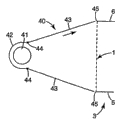
The photoconduction module of making like this is to be placed in the label casing, and the fluorescent tube of a long 14W of 60cm of adapted, and fluorescent tube is arranged in the case 25 of a high reflection, the long narrow side 7 of adjacent light guides module casing 3, and be arranged to its light directive photoconduction module.Now find: the uniformity that the front principal plane plate 5 of casing 3 is illuminated is very high, and the sufficient brightness that illuminates illuminates effectively will be placed on front panel 5 graphic picture before.
Example II
Made being similar to the described photoconduction module of example I, difference just, this photoconduction module is big, its size is about 120 * 180 * 6cm.In addition, the otpical leaf material 15 on the long narrow side 7 of casing 3 has been omitted, and the case 25 usefulness case 40 shown in Figure 6 of light source fluorescent tube 11 replaced, and this case with respect to the position of the long narrow side 7 of casing 3 also as shown in Figure 6.The illuminator shroud shell 40 that is independent of photoconduction casing 3 extends simultaneously also along the length of the side 7 of photoconduction casing 3 along the length of fluorescent tube (label 41 among Fig. 6) and extends.The two sides 43 that case 40 has the back 42 of close fluorescent tube 41 and 44 expansions of 42 leading edge extend to photoconduction casing 3 from the back.The two sides 43 of expansion form an outlet that supplies the light of fluorescent tube 41 from case 40 ejaculations.The back 42 of case 40 is configured as partly round fluorescent tube 41, but keeps proper spacing with it, and allows fluorescent tube to protrude in its leading edge 44 slightly, as shown in Figure 6.Back 42 shown in Fig. 6 is curved surfaces, but also can be the approximate curved surface that is made of many fillets plane.The inner surface of case 40 (that is inner surface of back 42 and side 43) covers with the efficient specular reflective material of one deck, for example above-mentioned " VM2000 Radiant Mirror Film ".
Be illuminated in the label at one that builds according to this example, find: the uniformity that the front principal plane plate 5 of casing 3 is illuminated is very high, and the sufficient brightness that illuminates illuminates effectively will be placed on front panel 5 graphic picture before.
Though above two examples and front description taken in conjunction with the accompanying drawings all are about the construction of photoconduction module, should be appreciated that, same photoconduction lighting fixture can be built directly in the casing of label and become its permanent part.
Neither be with the thin-film material that prism effect is arranged (such as above-mentioned Scotch
TMOpticalLighting Film) making the front panel 5 of photoconduction lighting fixture, is preferable with it certainly.Any material as long as its reflection and transmission coefficient can change with the incidence angle that light shines on it, all can be used for making front panel 5, comprises the plastic board of for example transparent polypropylene and so on.
It will also be appreciated that other material also can be used for the rear surface of optical cavities, as long as they are the narrow scattered reflection materials with enough highly reflectives.Be no more than 10 photoconduction lighting fixture for asperratio, it will be preferable that the narrow diffuse reflective materials of wide as far as possible folded light beam (that is the angle of flare of light beam is near 15 °) can be provided.But along with asperratio increases, the scattered reflection material that can produce narrower folded light beam also can provide the acceptable effect.In some cases, employing by different way the material of scattered reflection light beam (for example produce the light beam that obvious asymmetry is arranged, and light beam being parallel to before with the plane of rear board 5 and 6 in range of scatter greater than the range of scatter in the plane that is parallel to end face 7 and 8) be favourable.
Pointing out above, is 10 or to show its light output uniformity when bigger be not very good (though still can accept) according to the photoconduction lighting fixture of building in conjunction with the description of Fig. 1 to 3 in its asperratio.Especially, when observing the front panel 5 of photoconduction lighting fixture 1, can see that there is a zone that tangible brightness is higher at contiguous light source 11 places.If replace prismatic film 19 with above-mentioned transparent plastic plane lamina, this " edge glow " generally can be more obvious.But its available fairly simple method alleviates, and way is to apply light absorbing elements to the inner surface of the sheeting 19 of contiguous light source 11 (promptly facing the side of optical cavities 13).Light absorbing elements can be an element (for example many round dots) of for example using the printing of suitable printing ink (the opaque black ink that for example has the gloss reflection) formation.Surface coverage should be the highest (for example 70% of the covering surfaces area) in the edge of the direct contiguous light source 11 of thin slice 19, along with away from light source 11 linearly by subtracting, until being 0 leaving 150mm place, edge.This situation is shown in Fig. 5.Fig. 5 has expressed the light absorbing elements zone 30 of the contiguous light source 11 on the rear surface of sheeting 19.Light absorbing elements can directly be coated on the inner surface of front panel 5 of photoconduction lighting fixture 1, also can be coated in earlier on an independent transparent material (for example polyethylene) plate, then this piece plate is abutted on the inner surface of front panel 5.In each situation, all find, observe to adopt the photoconduction lighting fixture be illuminated label the time, light absorbing elements does not recognize.
Have been found that for most of label yardsticks the layout of above-mentioned light absorbing elements is that effectively therefore, if desired, it can be used as a standard part of all photoconduction lighting fixtures.If with the photoconduction lighting fixture of the sort of pattern shown in Figure 4, so at contiguous secondary light source 11 ' also need to locate arranged light absorber element.
Claims (9)
1. photoconduction lighting fixture, it comprises: a casing that forms the photoconduction optical cavities, described cavity has the first and second parallel main panels; And at least one is arranged to visible light is injected from a side of described casing the light source of cavity, and the light of injecting is directed between first and second main panel, it is characterized in that:
(a) first main panel comprises that the reflection of material and transmission coefficient are incident on the material that the angle on this material changes with light; And
(b) second main panel comprises narrow scattered reflection material, this material with the collimated light beam of incident be reflected into angle of flare less than 15 ° broaden light beam, and make the total reflectivity that is incident on its lip-deep visible light at any angle be at least 85%, described angle of flare is meant the direction of catoptrical high-high brightness and has angle or average angle between half the catoptrical direction of high-high brightness;
By this, can make light see through described first main panel equably to external exposure from described cavity inside.
2. photoconduction lighting fixture as claimed in claim 1 is characterized in that, described second main panel comprises the specular reflective material that is formed with optical scattering structure on it.
3. photoconduction lighting fixture as claimed in claim 1 is characterized in that, described second main panel comprises optical thin film or metallic plate.
4. photoconduction lighting fixture as claimed in claim 1 is characterized in that described second main panel comprises the sheeting of the inner surface that is posted by described casing.
5. as the described photoconduction lighting fixture of arbitrary claim in the claim 1 to 4, it is characterized in that, described first main panel has a side, a described side is made by the sheeting with grain surface, and described grain surface comprises away from a plurality of parallelogram prisms on the side of described optical cavities.
6. as the described photoconduction lighting fixture of arbitrary claim in the claim 1 to 4, it is characterized in that described first main panel has a side, a described side is made by the plane lamina that transparent material constitutes.
7. as the described photoconduction lighting fixture of arbitrary claim in the claim 1 to 4, it is characterized in that, also comprise the light absorbing elements that is applied on the zone described first main panel, contiguous described light source.
8. as the described photoconduction lighting fixture of arbitrary claim in the claim 1 to 4, it is characterized in that described light source is the elongate light source that extends along the side length of described cavity, the light of described light source passes described side and injects described cavity; Described light source has elongated case, and described case comprises:
A back, it be arranged on the behind of described light source and be configured as partly round described light source but and have between the described light source at interval; And
The side plate of two expansions, described side plate extend to the described side of described photoconduction cavity and form the outlet that light penetrates from elongated case from each leading edge at described back respectively,
Wherein, the described back of described light source case and the inner surface of described side plate comprise reflective material.
9. photoconduction lighting fixture as claimed in claim 8 is characterized in that, the side plate of described two expansions be arranged to make described outlet corresponding to and directly be adjacent to the described side of described optical cavities, thereby make light inject described optical cavities.
Applications Claiming Priority (2)
| Application Number | Priority Date | Filing Date | Title |
|---|---|---|---|
| GB0123813.8 | 2001-10-03 | ||
| GBGB0123813.8A GB0123813D0 (en) | 2001-10-03 | 2001-10-03 | Light-guide lights suitable for use in illuminated displays |
Publications (2)
| Publication Number | Publication Date |
|---|---|
| CN1639508A CN1639508A (en) | 2005-07-13 |
| CN100591988C true CN100591988C (en) | 2010-02-24 |
Family
ID=9923212
Family Applications (1)
| Application Number | Title | Priority Date | Filing Date |
|---|---|---|---|
| CN02819592A Expired - Fee Related CN100591988C (en) | 2001-10-03 | 2002-10-03 | Light-guide lights suitable for use in illuminated displays |
Country Status (9)
| Country | Link |
|---|---|
| US (1) | US7164836B2 (en) |
| EP (1) | EP1461564B1 (en) |
| JP (1) | JP4147189B2 (en) |
| CN (1) | CN100591988C (en) |
| AT (1) | ATE368198T1 (en) |
| AU (1) | AU2002341933A1 (en) |
| DE (1) | DE60221434T2 (en) |
| GB (1) | GB0123813D0 (en) |
| WO (1) | WO2003029723A2 (en) |
Families Citing this family (35)
| Publication number | Priority date | Publication date | Assignee | Title |
|---|---|---|---|---|
| GB0123813D0 (en) | 2001-10-03 | 2001-11-21 | 3M Innovative Properties Co | Light-guide lights suitable for use in illuminated displays |
| CN100530285C (en) * | 2003-10-23 | 2009-08-19 | 鸿富锦精密工业(深圳)有限公司 | Luminous sign plate |
| US7223005B2 (en) | 2003-12-23 | 2007-05-29 | Lamb David J | Hybrid lightguide backlight |
| US7303322B2 (en) | 2003-12-23 | 2007-12-04 | 3M Innovative Properties Company | Multiple lightguide backlight |
| US20050222801A1 (en) | 2004-04-06 | 2005-10-06 | Thomas Wulff | System and method for monitoring a mobile computing product/arrangement |
| US20060291241A1 (en) * | 2005-06-22 | 2006-12-28 | Carmanah Technologies Corp. | Light emitting diode illuminated display panel assembly |
| US20060289054A1 (en) * | 2005-06-22 | 2006-12-28 | Carmanah Technologies Corp. | Solar powered light emitting diode illuminated display panel assembly |
| NL1030161C2 (en) | 2005-10-11 | 2007-04-12 | Matthijs Dirk Meulenbelt | Presentation device. |
| US8594742B2 (en) * | 2006-06-21 | 2013-11-26 | Symbol Technologies, Inc. | System and method for monitoring a mobile device |
| KR101442275B1 (en) * | 2006-08-01 | 2014-09-22 | 쓰리엠 이노베이티브 프로퍼티즈 컴파니 | An illumination device and a vehicle glazing |
| US9028108B2 (en) * | 2007-05-20 | 2015-05-12 | 3M Innovative Properties Company | Collimating light injectors for edge-lit backlights |
| US8523419B2 (en) | 2007-05-20 | 2013-09-03 | 3M Innovative Properties Company | Thin hollow backlights with beneficial design characteristics |
| TW200916916A (en) * | 2007-05-20 | 2009-04-16 | 3M Innovative Properties Co | White light backlights and the like with efficient utilization of colored LED sources |
| KR101519171B1 (en) | 2007-05-20 | 2015-05-11 | 쓰리엠 이노베이티브 프로퍼티즈 컴파니 | Semi-specular components in hollow cavity light recycling backlights |
| US8469575B2 (en) | 2007-05-20 | 2013-06-25 | 3M Innovative Properties Company | Backlight and display system using same |
| EP2162770B1 (en) | 2007-06-14 | 2012-08-08 | Avery Dennison Corporation | Illuminated graphical and information display |
| TW200905311A (en) * | 2007-07-31 | 2009-02-01 | Chi Mei Lighting Tech Corp | Backlight module and application thereof |
| TW200916702A (en) * | 2007-10-11 | 2009-04-16 | Mustek Systems Inc | Light indicator |
| EP2255231A1 (en) * | 2008-02-07 | 2010-12-01 | 3M Innovative Properties Company | Hollow backlight with structured films |
| KR20100126389A (en) * | 2008-02-22 | 2010-12-01 | 쓰리엠 이노베이티브 프로퍼티즈 컴파니 | Backlights having selected output light flux distributions and display systems using same |
| JP5819723B2 (en) * | 2008-06-04 | 2015-11-24 | スリーエム イノベイティブ プロパティズ カンパニー | Hollow backlight with tilted light source |
| JP5600121B2 (en) | 2009-01-15 | 2014-10-01 | スリーエム イノベイティブ プロパティズ カンパニー | Light block |
| US20140022813A1 (en) * | 2009-12-03 | 2014-01-23 | Koninklijke Philips Electronics ,N.V. | Transparent Emissive Window Element |
| DE202010001843U1 (en) | 2010-02-03 | 2010-05-20 | 3M Innovative Properties Co., St. Paul | Playback device |
| US8568002B2 (en) * | 2010-03-05 | 2013-10-29 | Southpac Trust International Inc., Trustee of the LDH Trust | Light diffusion and condensing fixture |
| US20110219648A1 (en) * | 2010-03-12 | 2011-09-15 | Trevor James | Led edge-lit signage utilizing digital print technology |
| FR2967236B1 (en) * | 2010-11-04 | 2014-10-10 | Eurokera | LUMINOUS VITROCERAMIC ARTICLE |
| US8826572B2 (en) | 2012-03-30 | 2014-09-09 | Andy K. F. Kaoh | Adjustable illuminated lottery sign |
| CN102890306A (en) | 2012-10-11 | 2013-01-23 | 京东方科技集团股份有限公司 | Light guide plate and manufacturing method and forming mold of light guide plate |
| US9495892B2 (en) | 2013-08-21 | 2016-11-15 | Cooper Technologies Company | Light-emitting diode edge lighted airfield guidance sign |
| USD751648S1 (en) | 2013-08-21 | 2016-03-15 | Cooper Technologies Company | Light-emitting diode edge lighted airfield guidance sign |
| CN104597556A (en) * | 2014-12-02 | 2015-05-06 | 深圳市华星光电技术有限公司 | Light guide plate, backlight module and liquid crystal display device |
| US11119263B2 (en) | 2017-06-22 | 2021-09-14 | Xerox Corporation | System and method for image specific illumination of image printed on optical waveguide |
| US20180372630A1 (en) * | 2017-06-22 | 2018-12-27 | Xerox Corporation | System and method for image specific illumination of image printed on optical waveguide |
| US10748459B2 (en) | 2017-12-20 | 2020-08-18 | Andy K. F. Kaoh | Reduced cost lottery signs for displaying lottery jackpots of millions and billions of dollars |
Family Cites Families (16)
| Publication number | Priority date | Publication date | Assignee | Title |
|---|---|---|---|---|
| US4874228A (en) | 1987-03-24 | 1989-10-17 | Minnesota Mining And Manufacturing Company | Back-lit display |
| US4791540A (en) | 1987-05-26 | 1988-12-13 | Minnesota Mining And Manufacturing Company | Light fixture providing normalized output |
| GB2294350A (en) * | 1994-10-21 | 1996-04-24 | Sharp Kk | Light source and display |
| US6096375A (en) * | 1993-12-21 | 2000-08-01 | 3M Innovative Properties Company | Optical polarizer |
| US6080467A (en) * | 1995-06-26 | 2000-06-27 | 3M Innovative Properties Company | High efficiency optical devices |
| US5669700A (en) * | 1996-02-16 | 1997-09-23 | Exhibit-Group/Giltspur, Inc. | Light intensity equalizing element for lighted display panel |
| GB2310525A (en) | 1996-02-24 | 1997-08-27 | Ronnie Revell | Illuminated display device |
| US6473554B1 (en) * | 1996-12-12 | 2002-10-29 | Teledyne Lighting And Display Products, Inc. | Lighting apparatus having low profile |
| US6096247A (en) * | 1998-07-31 | 2000-08-01 | 3M Innovative Properties Company | Embossed optical polymer films |
| US6259561B1 (en) * | 1999-03-26 | 2001-07-10 | The University Of Rochester | Optical system for diffusing light |
| KR20020001858A (en) | 1999-04-28 | 2002-01-09 | 캐롤린 에이. 베이츠 | Shallow depth back lit illuminated signage |
| GB0006327D0 (en) | 2000-03-16 | 2000-05-03 | 3M Innovative Properties Co | Light guides suitable for illuminated displays |
| FR2820235B1 (en) * | 2001-01-26 | 2003-06-13 | Thomson Csf | BACKLIGHT DEVICE FOR VIEWING SCREEN BY TRANSMISSION COMPATIBLE WITH NIGHT VISION |
| GB0123813D0 (en) | 2001-10-03 | 2001-11-21 | 3M Innovative Properties Co | Light-guide lights suitable for use in illuminated displays |
| US6866678B2 (en) * | 2002-12-10 | 2005-03-15 | Interbational Technology Center | Phototherapeutic treatment methods and apparatus |
| US6950454B2 (en) * | 2003-03-24 | 2005-09-27 | Eastman Kodak Company | Electronic imaging system using organic laser array illuminating an area light valve |
-
2001
- 2001-10-03 GB GBGB0123813.8A patent/GB0123813D0/en not_active Ceased
-
2002
- 2002-10-03 EP EP02776093A patent/EP1461564B1/en not_active Expired - Lifetime
- 2002-10-03 WO PCT/US2002/031419 patent/WO2003029723A2/en active IP Right Grant
- 2002-10-03 CN CN02819592A patent/CN100591988C/en not_active Expired - Fee Related
- 2002-10-03 US US10/491,097 patent/US7164836B2/en not_active Expired - Fee Related
- 2002-10-03 AT AT02776093T patent/ATE368198T1/en not_active IP Right Cessation
- 2002-10-03 JP JP2003532900A patent/JP4147189B2/en not_active Expired - Fee Related
- 2002-10-03 AU AU2002341933A patent/AU2002341933A1/en not_active Abandoned
- 2002-10-03 DE DE60221434T patent/DE60221434T2/en not_active Expired - Lifetime
Also Published As
| Publication number | Publication date |
|---|---|
| JP2005505106A (en) | 2005-02-17 |
| WO2003029723A2 (en) | 2003-04-10 |
| EP1461564A2 (en) | 2004-09-29 |
| US7164836B2 (en) | 2007-01-16 |
| AU2002341933A1 (en) | 2003-04-14 |
| ATE368198T1 (en) | 2007-08-15 |
| DE60221434D1 (en) | 2007-09-06 |
| WO2003029723A3 (en) | 2004-07-22 |
| DE60221434T2 (en) | 2008-04-10 |
| EP1461564B1 (en) | 2007-07-25 |
| GB0123813D0 (en) | 2001-11-21 |
| JP4147189B2 (en) | 2008-09-10 |
| US20050175282A1 (en) | 2005-08-11 |
| CN1639508A (en) | 2005-07-13 |
Similar Documents
| Publication | Publication Date | Title |
|---|---|---|
| CN100591988C (en) | Light-guide lights suitable for use in illuminated displays | |
| US11821621B2 (en) | Method of making light guide illumination systems with enhanced light coupling | |
| US5461547A (en) | Flat panel display lighting system | |
| US5485354A (en) | Flat panel display lighting system | |
| EP0453092B1 (en) | Uniform illumination of large, thin surfaces particularly suited for automotive applications | |
| US7172324B2 (en) | Internally illuminated light panel with LED modules having light redirecting devices | |
| US5926601A (en) | Stacked backlighting system using microprisms | |
| KR100501066B1 (en) | Surface light source device of side light type | |
| US4277817A (en) | Large-area light source | |
| KR100939854B1 (en) | Light-guide lights providing a substantially monochromatic beam | |
| US7110060B2 (en) | Assemblies and methods for illuminating a display | |
| CN100520160C (en) | Backlight device and liquid crystal display | |
| US7493010B1 (en) | Stepped light guide | |
| TW454100B (en) | Light-source element with inclined light-coupling in side | |
| US10012783B2 (en) | Lighting system using a light guide and a lighting method | |
| KR20000029047A (en) | Sidelight type surface light source device and liquid-crystal display device | |
| KR100729193B1 (en) | Sidelight type surface light source apparatus | |
| US20050281053A1 (en) | Light generating device comprising light input and light output units | |
| WO2004031818A2 (en) | Light source assembly and light-guide light suitable for an illuminated display | |
| JPH09138309A (en) | Uniformly thin high-efficiency large-area illumination panel | |
| JPH05158036A (en) | Surface illuminating device for liquid crystal display device | |
| JPH1049064A (en) | Lighting device |
Legal Events
| Date | Code | Title | Description |
|---|---|---|---|
| C06 | Publication | ||
| PB01 | Publication | ||
| C10 | Entry into substantive examination | ||
| SE01 | Entry into force of request for substantive examination | ||
| C14 | Grant of patent or utility model | ||
| GR01 | Patent grant | ||
| CF01 | Termination of patent right due to non-payment of annual fee |
Granted publication date: 20100224 Termination date: 20181003 |
|
| CF01 | Termination of patent right due to non-payment of annual fee |