CN100583193C - Manufacturing method of display device - Google Patents
Manufacturing method of display device Download PDFInfo
- Publication number
- CN100583193C CN100583193C CN200480035192A CN200480035192A CN100583193C CN 100583193 C CN100583193 C CN 100583193C CN 200480035192 A CN200480035192 A CN 200480035192A CN 200480035192 A CN200480035192 A CN 200480035192A CN 100583193 C CN100583193 C CN 100583193C
- Authority
- CN
- China
- Prior art keywords
- substrate
- film
- display device
- oxidation film
- optical filter
- Prior art date
- Legal status (The legal status is an assumption and is not a legal conclusion. Google has not performed a legal analysis and makes no representation as to the accuracy of the status listed.)
- Expired - Fee Related
Links
Images


Classifications
-
- H—ELECTRICITY
- H01—ELECTRIC ELEMENTS
- H01L—SEMICONDUCTOR DEVICES NOT COVERED BY CLASS H10
- H01L33/00—Semiconductor devices with at least one potential-jump barrier or surface barrier specially adapted for light emission; Processes or apparatus specially adapted for the manufacture or treatment thereof or of parts thereof; Details thereof
- H01L33/005—Processes
-
- G—PHYSICS
- G02—OPTICS
- G02F—OPTICAL DEVICES OR ARRANGEMENTS FOR THE CONTROL OF LIGHT BY MODIFICATION OF THE OPTICAL PROPERTIES OF THE MEDIA OF THE ELEMENTS INVOLVED THEREIN; NON-LINEAR OPTICS; FREQUENCY-CHANGING OF LIGHT; OPTICAL LOGIC ELEMENTS; OPTICAL ANALOGUE/DIGITAL CONVERTERS
- G02F1/00—Devices or arrangements for the control of the intensity, colour, phase, polarisation or direction of light arriving from an independent light source, e.g. switching, gating or modulating; Non-linear optics
- G02F1/01—Devices or arrangements for the control of the intensity, colour, phase, polarisation or direction of light arriving from an independent light source, e.g. switching, gating or modulating; Non-linear optics for the control of the intensity, phase, polarisation or colour
- G02F1/13—Devices or arrangements for the control of the intensity, colour, phase, polarisation or direction of light arriving from an independent light source, e.g. switching, gating or modulating; Non-linear optics for the control of the intensity, phase, polarisation or colour based on liquid crystals, e.g. single liquid crystal display cells
- G02F1/133—Constructional arrangements; Operation of liquid crystal cells; Circuit arrangements
- G02F1/1333—Constructional arrangements; Manufacturing methods
- G02F1/133305—Flexible substrates, e.g. plastics, organic film
-
- G—PHYSICS
- G02—OPTICS
- G02F—OPTICAL DEVICES OR ARRANGEMENTS FOR THE CONTROL OF LIGHT BY MODIFICATION OF THE OPTICAL PROPERTIES OF THE MEDIA OF THE ELEMENTS INVOLVED THEREIN; NON-LINEAR OPTICS; FREQUENCY-CHANGING OF LIGHT; OPTICAL LOGIC ELEMENTS; OPTICAL ANALOGUE/DIGITAL CONVERTERS
- G02F1/00—Devices or arrangements for the control of the intensity, colour, phase, polarisation or direction of light arriving from an independent light source, e.g. switching, gating or modulating; Non-linear optics
- G02F1/01—Devices or arrangements for the control of the intensity, colour, phase, polarisation or direction of light arriving from an independent light source, e.g. switching, gating or modulating; Non-linear optics for the control of the intensity, phase, polarisation or colour
- G02F1/13—Devices or arrangements for the control of the intensity, colour, phase, polarisation or direction of light arriving from an independent light source, e.g. switching, gating or modulating; Non-linear optics for the control of the intensity, phase, polarisation or colour based on liquid crystals, e.g. single liquid crystal display cells
- G02F1/133—Constructional arrangements; Operation of liquid crystal cells; Circuit arrangements
- G02F1/1333—Constructional arrangements; Manufacturing methods
-
- H—ELECTRICITY
- H01—ELECTRIC ELEMENTS
- H01L—SEMICONDUCTOR DEVICES NOT COVERED BY CLASS H10
- H01L27/00—Devices consisting of a plurality of semiconductor or other solid-state components formed in or on a common substrate
- H01L27/02—Devices consisting of a plurality of semiconductor or other solid-state components formed in or on a common substrate including semiconductor components specially adapted for rectifying, oscillating, amplifying or switching and having at least one potential-jump barrier or surface barrier; including integrated passive circuit elements with at least one potential-jump barrier or surface barrier
- H01L27/12—Devices consisting of a plurality of semiconductor or other solid-state components formed in or on a common substrate including semiconductor components specially adapted for rectifying, oscillating, amplifying or switching and having at least one potential-jump barrier or surface barrier; including integrated passive circuit elements with at least one potential-jump barrier or surface barrier the substrate being other than a semiconductor body, e.g. an insulating body
- H01L27/1214—Devices consisting of a plurality of semiconductor or other solid-state components formed in or on a common substrate including semiconductor components specially adapted for rectifying, oscillating, amplifying or switching and having at least one potential-jump barrier or surface barrier; including integrated passive circuit elements with at least one potential-jump barrier or surface barrier the substrate being other than a semiconductor body, e.g. an insulating body comprising a plurality of TFTs formed on a non-semiconducting substrate, e.g. driving circuits for AMLCDs
- H01L27/1259—Multistep manufacturing methods
- H01L27/1262—Multistep manufacturing methods with a particular formation, treatment or coating of the substrate
- H01L27/1266—Multistep manufacturing methods with a particular formation, treatment or coating of the substrate the substrate on which the devices are formed not being the final device substrate, e.g. using a temporary substrate
-
- H—ELECTRICITY
- H01—ELECTRIC ELEMENTS
- H01L—SEMICONDUCTOR DEVICES NOT COVERED BY CLASS H10
- H01L27/00—Devices consisting of a plurality of semiconductor or other solid-state components formed in or on a common substrate
- H01L27/15—Devices consisting of a plurality of semiconductor or other solid-state components formed in or on a common substrate including semiconductor components with at least one potential-jump barrier or surface barrier specially adapted for light emission
-
- H—ELECTRICITY
- H10—SEMICONDUCTOR DEVICES; ELECTRIC SOLID-STATE DEVICES NOT OTHERWISE PROVIDED FOR
- H10K—ORGANIC ELECTRIC SOLID-STATE DEVICES
- H10K50/00—Organic light-emitting devices
- H10K50/80—Constructional details
- H10K50/84—Passivation; Containers; Encapsulations
- H10K50/841—Self-supporting sealing arrangements
-
- H—ELECTRICITY
- H10—SEMICONDUCTOR DEVICES; ELECTRIC SOLID-STATE DEVICES NOT OTHERWISE PROVIDED FOR
- H10K—ORGANIC ELECTRIC SOLID-STATE DEVICES
- H10K59/00—Integrated devices, or assemblies of multiple devices, comprising at least one organic light-emitting element covered by group H10K50/00
- H10K59/10—OLED displays
- H10K59/12—Active-matrix OLED [AMOLED] displays
-
- H—ELECTRICITY
- H10—SEMICONDUCTOR DEVICES; ELECTRIC SOLID-STATE DEVICES NOT OTHERWISE PROVIDED FOR
- H10K—ORGANIC ELECTRIC SOLID-STATE DEVICES
- H10K59/00—Integrated devices, or assemblies of multiple devices, comprising at least one organic light-emitting element covered by group H10K50/00
- H10K59/30—Devices specially adapted for multicolour light emission
- H10K59/38—Devices specially adapted for multicolour light emission comprising colour filters or colour changing media [CCM]
-
- H—ELECTRICITY
- H10—SEMICONDUCTOR DEVICES; ELECTRIC SOLID-STATE DEVICES NOT OTHERWISE PROVIDED FOR
- H10K—ORGANIC ELECTRIC SOLID-STATE DEVICES
- H10K71/00—Manufacture or treatment specially adapted for the organic devices covered by this subclass
-
- H—ELECTRICITY
- H10—SEMICONDUCTOR DEVICES; ELECTRIC SOLID-STATE DEVICES NOT OTHERWISE PROVIDED FOR
- H10K—ORGANIC ELECTRIC SOLID-STATE DEVICES
- H10K71/00—Manufacture or treatment specially adapted for the organic devices covered by this subclass
- H10K71/80—Manufacture or treatment specially adapted for the organic devices covered by this subclass using temporary substrates
-
- H—ELECTRICITY
- H10—SEMICONDUCTOR DEVICES; ELECTRIC SOLID-STATE DEVICES NOT OTHERWISE PROVIDED FOR
- H10K—ORGANIC ELECTRIC SOLID-STATE DEVICES
- H10K77/00—Constructional details of devices covered by this subclass and not covered by groups H10K10/80, H10K30/80, H10K50/80 or H10K59/80
- H10K77/10—Substrates, e.g. flexible substrates
-
- H—ELECTRICITY
- H01—ELECTRIC ELEMENTS
- H01L—SEMICONDUCTOR DEVICES NOT COVERED BY CLASS H10
- H01L2933/00—Details relating to devices covered by the group H01L33/00 but not provided for in its subgroups
- H01L2933/0008—Processes
- H01L2933/0025—Processes relating to coatings
-
- H—ELECTRICITY
- H10—SEMICONDUCTOR DEVICES; ELECTRIC SOLID-STATE DEVICES NOT OTHERWISE PROVIDED FOR
- H10K—ORGANIC ELECTRIC SOLID-STATE DEVICES
- H10K59/00—Integrated devices, or assemblies of multiple devices, comprising at least one organic light-emitting element covered by group H10K50/00
- H10K59/10—OLED displays
- H10K59/12—Active-matrix OLED [AMOLED] displays
- H10K59/1201—Manufacture or treatment
-
- Y—GENERAL TAGGING OF NEW TECHNOLOGICAL DEVELOPMENTS; GENERAL TAGGING OF CROSS-SECTIONAL TECHNOLOGIES SPANNING OVER SEVERAL SECTIONS OF THE IPC; TECHNICAL SUBJECTS COVERED BY FORMER USPC CROSS-REFERENCE ART COLLECTIONS [XRACs] AND DIGESTS
- Y02—TECHNOLOGIES OR APPLICATIONS FOR MITIGATION OR ADAPTATION AGAINST CLIMATE CHANGE
- Y02E—REDUCTION OF GREENHOUSE GAS [GHG] EMISSIONS, RELATED TO ENERGY GENERATION, TRANSMISSION OR DISTRIBUTION
- Y02E10/00—Energy generation through renewable energy sources
- Y02E10/50—Photovoltaic [PV] energy
- Y02E10/549—Organic PV cells
-
- Y—GENERAL TAGGING OF NEW TECHNOLOGICAL DEVELOPMENTS; GENERAL TAGGING OF CROSS-SECTIONAL TECHNOLOGIES SPANNING OVER SEVERAL SECTIONS OF THE IPC; TECHNICAL SUBJECTS COVERED BY FORMER USPC CROSS-REFERENCE ART COLLECTIONS [XRACs] AND DIGESTS
- Y02—TECHNOLOGIES OR APPLICATIONS FOR MITIGATION OR ADAPTATION AGAINST CLIMATE CHANGE
- Y02P—CLIMATE CHANGE MITIGATION TECHNOLOGIES IN THE PRODUCTION OR PROCESSING OF GOODS
- Y02P70/00—Climate change mitigation technologies in the production process for final industrial or consumer products
- Y02P70/50—Manufacturing or production processes characterised by the final manufactured product
Abstract
To provide a method of manufacturing a display device having an excellent impact resistance property with high yield, in particular, a method of manufacturing a display device having an optical film that is formed using a plastic substrate. The method of manufacturing a display device includes the steps of: laminating a metal film, an oxide film, and an optical filter on a first substrate; separating the optical filter from the first substrate; attaching the optical filter to a second substrate; forming a layer including a pixel on a third substrate; and attaching the layer including the pixel to the optical filter.
Description
Technical field
The present invention relates to make the method for display device with the optical thin film that uses plastic base formation.
Background technology
In recent years, the technology of using the semiconductive thin film (thickness is that some approximately nanometers are to the hundreds of nanometer) that forms with insulating surface on substrate to form thin film transistor (TFT) (TFT) has caused attention.Thin film transistor (TFT) has been widely used in the various electronic equipments such as IC and electronic installation.Especially, relate to as the exploitation of thin film transistor (TFT) of the on-off element that is used for LCDs or light emitting display and carrying out fast.
In LCDs, liquid crystal display material is clipped in device substrate (elementsubstrate) and the relative substrate (opposingsubstrate) with opposite electrode that is placed on the device substrate opposite.On device substrate, use amorphous silicon or polysilicon to be arranged in array, and form pixel electrode, source connection and the grid connection that links to each other with each TFT respectively as its semi-conductive TFT.Be used to carry out color filter that color shows at device substrate or form on the substrate relatively.Polaroid is arranged as optical gate respectively on device substrate and relative substrate, with color display.
The color filter of LCDs comprises by R (red), G (green), the dyed layer that B (indigo plant) forms, the light shield mask (black matrix) that is used to cover gap between the pixel, and passes by emission light and wherein to extract red, green, blue.The light shield mask of color filter is made by metal film that comprises carbon black or organic film usually.Color filter is arranged on the position corresponding with pixel, will be the color of the light of each pixel extraction thereby can change.Note, represent the part consistent with pixel electrode with the position that pixel is corresponding.
In light-emitting display apparatus, a kind of colorize method that is arranged in matrix by the light-emitting component that will launch red, green and blue light is respectively arranged; The colorize method of the color filter of the light-emitting component by utilize using the emission white light etc.Colorize method by colorize method that utilizes the color filter that uses the light-emitting component of launching white light and the liquid crystal display that uses color filter is gone up similar in principle (referring to patent file 1).Patent file 1: Japanese Patent Application Publication No.2001-217072.
Summary of the invention
Usually, the color filter that is used for liquid crystal display has been formed on glass substrate.Therefore, such problem is arranged: be formed on the color filter on the glass substrate and use the poor impact resistance of the liquid crystal display of this color filter.In addition, when the thickness that reduces glass substrate when reducing the thickness of liquid crystal display, thereby substrate may break and causes output to descend.
In addition, because glass substrate does not have flexibility, so be difficult to form colorful film having on the display device of curved surface.
Pigmentary resin and pigment dispersing resin are used as the original material of color filter usually.Yet,, need the step of heating at normal temperatures in order to solidify these resins.Therefore, it is difficult forming color filter on the thermoplasticity substrate.
According to the problems referred to above, the purpose of this invention is to provide the method that the display device with preferable shock-resistant attribute is made on high yield ground, promptly make the method for display device with the optical thin film that uses plastic base formation.
According to an aspect of the present invention, provide the method for making display device, having comprised: first step, lamination metal film, oxidation film and optical filter on first substrate; Second step is attached to second substrate on the optical filter; Third step is peeled off first substrate from optical filter; And the 4th step, first forms the layer that comprises pixel on the surface of the 3rd substrate after third step, and optical filter is labelled on the another side of the layer that comprises pixel.
According to a further aspect in the invention, provide a kind of method of making display device, having comprised: first step, lamination first metal film, first oxidation film and optical filter on first substrate; Second step, with optical filter from first strippable substrate; Third step is attached to second substrate on the optical filter; The 4th step, first forms the layer that comprises pixel on lamination second metal film and second oxidation film on the 3rd substrate, surface at oxidation film after third step, and the laminating that comprises pixel is to optical filter; And the 5th step, second metal film is peeled off from second oxidation film, and tetrabasal is labelled on another surface of peeling off second oxidation film.
Note, can after carrying out first and second steps, carry out third step.Also can after execution first and third step, carry out second step.
Display device such as liquid crystal display, light-emitting display apparatus, DMD (digital micromirror device), PDP (plasma display panel (PDP)), FED (Field Emission Display), electro phoretic display device (Electronic Paper) can be listed as the representative illustration of display device.
In the situation of using liquid crystal display, liquid crystal display material is filled between pixel electrode and the optical filter.Pixel electrode can be arranged on the optical filter.When pixel electrode only when a side of liquid crystal material forms, liquid crystal display is to carry out the equipment that the IPS pattern shows.When providing when liquid crystal material sandwiched therebetween two pixel electrodes, liquid crystal display is to carry out that TN (twisted nematic) pattern shows, STN (STN Super TN) pattern shows and VA (vertical alignment) pattern shows.
In the situation of using light-emitting display apparatus, first electrode, second electrode and the layer that comprises luminescent substance that provides between electrode are provided light-emitting component, wherein first electrode is arranged on the 3rd substrate, second electrode be arranged on the 3rd substrate opposing substrates (i.e. second substrate or tetrabasal) on.Light-emitting component with this structure is carried out passive matrix driving demonstration.Perhaps, comprise first pixel electrode at light-emitting component, comprise the layer of luminescent substance and be arranged in the situation of second pixel electrode on the 3rd substrate, the light-emitting component with this structure is carried out driven with active matrix and is shown.
Optical filter is color filter, color conversion optical filter or holographic color filters.
Second substrate is made with plastic base.In this case, the optical thin film that comprises second substrate and optical filter is the film with color filter, color conversion optical filter or holographic color filters.
Optical thin film can be used as second substrate.For optical thin film, film, diaphragm, brightness improvement film, prism plate etc. are improved in the circularly polarizing plate of can adopt polaroid, being made up of phase retardation plate and polaroid or ellipsoidal polarizing plate, anti-reflective film, visual angle.The optical thin film that comprises optical filter and tetrabasal represents multiple optical properties.
The present invention also comprises following aspect.
According to an aspect of the present invention, a kind of method of making display device is provided, comprise: first step, lamination first metal film, first oxidation film and optical filter according to the order of sequence on first substrate, by use the first peelable bonding agent that first support media is labelled to make on the surface of optical filter first support media by optical filter towards first substrate, and first metal film is peeled off from first oxidation film by physical means; Second step forms the layer that comprises pixel on second substrate; And third step, after first and second steps, first oxidation film is labelled on the surface of layer of the pixel that comprises second substrate, and removes the first peelable bonding agent and first support media.
After third step, the 3rd substrate can be labelled on the surface of optical filter by using second cohesive material.
In this case; first and second substrates are any of quartz base plate, ceramic substrate, silicon substrate, metal substrate and stainless steel substrate, and the 3rd substrate be plastics, polaroid, polaroid (ellipsoidal polarizing plate or circularly polarizing plate), anti-reflective film, visual angle with phase retardation plate improve film, diaphragm, brightness improvement film, prism plate etc.
In second step or third step, the surface of second substrate can stick plastics, polaroid, have the polaroid of phase retardation plate (ellipsoidal polarizing plate or circularly polarizing plate), anti-reflective film, visual angle improve film, diaphragm, brightness improvement film, prism plate etc.
In addition, according to a further aspect in the invention, a kind of method of making display device is provided, comprise: first step, lamination first metal film, first oxidation film and optical filter according to the order of sequence on first substrate, by use first cohesive material that second substrate is labelled to make on the surface of optical filter second substrate by optical filter towards first substrate, by using the first peelable bonding agent that first support media is labelled on the surface of second substrate, and first metal film is peeled off from first oxidation film so that form optical thin film by physical means; Second step forms the layer that comprises pixel on the 3rd substrate; And third step, after first and second steps, first oxidation film is labelled on the surface of layer of the pixel that comprises the 3rd substrate, and removes the first peelable bonding agent and first support media.
In addition, according to a further aspect in the invention, a kind of method of making display device is provided, comprise: first step, lamination first metal film according to the order of sequence on first substrate, first oxidation film and optical filter, by use the first peelable bonding agent that first support media is labelled to make on the surface of optical filter first support media by optical filter towards first substrate, by physical means first metal film is peeled off from first oxidation film, by using first cohesive material that second substrate is labelled on the surface of first oxidation film, and remove first support media and the first peelable bonding agent so that form optical thin film; Second step forms the layer that comprises pixel on the 3rd substrate; And third step, on the surface of layer by the pixel using second cohesive material that optical filter is labelled to comprise the 3rd substrate after first and second steps.
The first and the 3rd substrate is any of quartz base plate, ceramic substrate, silicon substrate, metal substrate and stainless steel substrate, and second substrate be plastics, polaroid, polaroid (ellipsoidal polarizing plate or circularly polarizing plate), anti-reflective film, visual angle with phase retardation plate improve in film, diaphragm, brightness improvement film, the prism plate etc. any.
After second step and third step, the surface of the 3rd substrate can stick plastics, polaroid, have the polaroid of phase retardation plate (ellipsoidal polarizing plate or circularly polarizing plate), anti-reflective film, visual angle improve film, diaphragm, brightness improvement film, prism plate etc.
In addition, according to another aspect of the invention, a kind of method of making display device is provided, comprise: first step, lamination first metal film, first oxidation film and optical filter according to the order of sequence on first substrate, by use the first peelable bonding agent that first support media is labelled to make on the surface of optical filter first support media by optical filter towards first substrate, by physical means first metal film is peeled off from first oxidation film; Second step, lamination second metal film and second oxidation film according to the order of sequence on second substrate, and on second oxidation film, form pixel electrode; And third step, on the surface of layer by the pixel using first cohesive material that first oxidation film is labelled to comprise second substrate after first and second steps, by using physical means second metal film is peeled off from second oxidation film, by using second cohesive material that the 3rd substrate is labelled on the surface of second oxidation film, and remove the first peelable bonding agent and first support media.
After third step, tetrabasal can be labelled on the surface of light filter by using the 3rd cohesive material.
In this case; first and second substrates are any of quartz base plate, ceramic substrate, silicon substrate, metal substrate and stainless steel substrate, and third and fourth substrate be plastics, polaroid, polaroid (ellipsoidal polarizing plate or circularly polarizing plate), anti-reflective film, visual angle with phase retardation plate improve any of film, diaphragm, brightness improvement film, prism plate etc.
In addition, according to a further aspect in the invention, a kind of method of making display device is provided, comprise: first step, lamination first metal film, first oxidation film and optical filter according to the order of sequence on first substrate, by use first cohesive material that second substrate is labelled to make on the surface of optical filter second substrate by optical filter towards first substrate, by using the first peelable bonding agent that first support media is labelled on the surface of second substrate, and first metal film is peeled off from first oxidation film so that form optical thin film by physical means; Second step, lamination second metal film and second oxidation film according to the order of sequence on the 3rd substrate, and on second oxidation film, form the layer that comprises pixel; And third step, on the surface of layer by the pixel using second cohesive material that first oxidation film is labelled to comprise the 3rd substrate after first and second steps, by physical means second metal film is peeled off from second oxidation film, by using the 3rd cohesive material that tetrabasal is labelled on the surface of second oxidation film, and remove the first peelable bonding agent and first support media.
In addition, another aspect according to this aspect, a kind of method of making display device is provided, comprise: first step, lamination first metal film, first oxidation film and optical filter according to the order of sequence on first substrate, by use the first peelable bonding agent that first support media is labelled to make on the surface of optical filter first supporting substrates by optical filter towards first substrate, and first metal film is peeled off from first oxidation film by physical means; Second step is labelled to second substrate on the surface of first oxidation film by using first cohesive material, and removes first support media and the first peelable bonding agent so that form optical thin film; Third step, lamination second metal film and second oxidation film according to the order of sequence on the 3rd substrate, and on second oxidation film, form the layer that comprises pixel; And the 4th step, first after third step on the surface of the layer by using second cohesive material that optical filter is labelled to comprise pixel, by physical means second metal film is peeled off from second oxidation film, tetrabasal is labelled on the surface of second oxidation film by using the 3rd cohesive material.
With form first metal film and first oxidation film side by side, first metal oxide film can form between first metal film and first oxidation film.In addition, and form second metal film and second oxidation film side by side, second metal oxide film can form between second metal film and second oxidation film.
First oxidation film can be on the surface of oxidation first metal film to form after forming first metal oxide film.Similarly, second oxidation film can be on the surface of oxidation second metal film to form after forming second metal oxide film.
In addition, semiconductor element is electrically connected with pixel electrode.For semiconductor element, use TFT, organic semiconductor transistor, diode, MIM element etc.
First substrate is heat resistant substrate preferably.Usually, glass substrate, quartz base plate, ceramic substrate, silicon substrate, metal substrate and stainless steel substrate can be used as first substrate.
First and second metal films can use the element of selecting from titanium (Ti), aluminium (Al), tantalum (Ta), tungsten (W), molybdenum (Mo), copper (Cu), chromium (Cr), neodymium (Nd), iron (Fe), nickel (Ne), cobalt (Co), ruthenium (Ru), rhodium (Rh), palladium (Pd), osmium (Os), iridium (Ir) to make; Availablely comprise above-mentioned element and make as the alloy material of its Main Ingredients and Appearance or the simple layer of compound-material; Available its laminate layers is made; Or make with its nitride.
In addition, after the formation isolating bar, it can be attached on the second or the 3rd substrate on the surface of the layer that comprises pixel.
According to the present invention, display device refers to use the equipment of display element, i.e. image display.In addition, display device comprises following whole module: with the module that joint links to each other with liquid crystal cell, for example flexible print circuit (FPC), TAB (flexible band is from being dynamically connected) are with or TCP (chip belt carries encapsulation); Module with the printed wiring board that provides in the end of TAB band or TCP; And with display element directly and the module that is installed together of IC (integrated circuit) or CPU by COG (glass top chip) technology.
According to the present invention, can form display device with the optical thin film that comprises plastic base.As a result, can form lightweight, thin type display device with preferable shock-resistant attribute.In addition, can make the display device with curved surface or the display device of shape variable.
In the display device that uses according to optical thin film of the present invention, comprise that the layer and the optical thin film of pixel forms separately by different step, after finishing, fit each other again.By using this structure, can control the output of display element or semiconductor element and the output of optical thin film separately, thereby suppress the decline of whole display device output.
In addition, make the step of active-matrix substrate and the step of manufacturing optical thin film and can move simultaneously, thus the manufacturing delivery cycle of shortening display device.
Description of drawings
Figure 1A~1E is that the cross sectional view according to the step of display device of the present invention is made in explanation;
Fig. 2 A~2F is that the cross sectional view according to the step of display device of the present invention is made in explanation;
Fig. 3 A~3F is that the cross sectional view according to the step of display device of the present invention is made in explanation;
Fig. 4 A~4E is that the cross sectional view according to the step of display device of the present invention is made in explanation;
Fig. 5 A~5D is that the cross sectional view according to the step of display device of the present invention is made in explanation;
Fig. 6 A and 6B are that the cross sectional view according to the step of display device of the present invention is made in explanation;
Fig. 7 A and 7B are that the cross sectional view according to the step of display device of the present invention is made in explanation;
Fig. 8 A and 8B are that the cross sectional view according to the step of display device of the present invention is made in explanation;
Fig. 9 A~9C is that the cross sectional view according to the step of display device of the present invention is made in explanation;
Figure 10 A and 10B are that the cross sectional view according to the step of display device of the present invention is made in explanation;
Figure 11 A and 11B are that the cross sectional view according to the step of display device of the present invention is made in explanation;
Figure 12 A is the vertical view that display screen constructed in accordance is shown, and Figure 12 B is a cross sectional view;
Figure 13 A is the vertical view that display screen constructed in accordance is shown, and Figure 13 B is a cross sectional view;
Figure 14 A and 14B are the diagrammatic sketch that light emitting element structure is shown;
Figure 15 A~15C is the circuit diagram of the pixel of light-emitting component;
Figure 16 A is the vertical view that display screen constructed in accordance is shown, and Figure 16 B is a cross sectional view;
Figure 17 A is the vertical view that display screen constructed in accordance is shown, and Figure 17 B is a cross sectional view;
Figure 18 is the diagrammatic sketch of explanation one electronic devices structure;
Figure 19 is the diagrammatic sketch of explanation one electronic equipment example;
Figure 20 A and 20B are the diagrammatic sketch of explanation one electronic equipment example.
Embodiment
Embodiment 1
The method that manufacturing has the display device of the optical thin film that uses plastic base formation is described with present embodiment with reference to Figure 1A~1E.
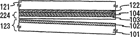
Shown in Figure 1A, first metal film 102 forms on first substrate 101.As first substrate, can use heat proof material, can bear heat treated material in follow-up manufacturing optical filter and the strip step, be generally glass substrate, quartz base plate, ceramic substrate, silicon substrate, metal substrate or stainless steel substrate.
Then first oxidation film 103 forms on first metal film 102.In this case, first metal oxide film forms between first metal film 102 and first oxidation film 103.During strip step in carrying out subsequent step, peeling off can be in first metal oxide film, carry out in the interface between first metal oxide film and first oxidation film or the interface between first metal oxide film and first metal film.For first metal oxide film 103, layer can be made by silicon dioxide, silicon oxynitride or metal oxide by spraying plating or plasma CVD.The thickness of first oxidation film 103 is preferably than first metal film, 102 thick twices at least, more preferably than first metal film 102 thick four times.The thickness of first oxidation film 103 is set to 200~800 nanometers at this, preferably is set to 200~300 nanometers.
Then optical filter 104 forms on first oxidation film 103.As representative illustration, can enumerate optical filter, color filter, color conversion optical filter, holographic color filters etc.
Plastic base (film that macromolecular material or resin are made) is used as second substrate 112.As the representative illustration of plastic base, ARTON, polyethylene terephthalate (PET), polyethersulfone (PES), poly-naphthoic acid glycol ester (PEN), nylon, polyetheretherketone (PEEK), polysulfones (PSF), polyetherimide (PEI), polyarylate (PAR), polybutylene terephthalate (PBT) and the polyimide that can use the norcamphane resin made such as polycarbonate (PC), by JSR company to make with polar group.In addition, the optical thin film such as polaroid, the polaroid (ellipsoidal polarizing plate or circularly polarizing plate) with phase retardation plate, anti-reflective film, visual angle improvement film, diaphragm, brightness improvement film, prism plate etc. can be used as second substrate.
Then, first support media, 121 usefulness, the first peelable bonding agent is attached to the surface of second substrate 112.At this moment, when bubble is invaded between second substrate 112 and the first peelable bonding agent 122, optical filter will break in follow-up strip step easily.In order to prevent to break, stick first support media not produce bubble betwixt.Add first support media and do not sneak into bubble betwixt by using dress carrying device etc., can pasting at short notice.
Preferably, the substrate that has higher rigidity than first substrate 101 and second substrate 112 is used as first support media 121, is generally quartz base plate, metal substrate or ceramic substrate.
For the first peelable alite paste 122, can use the cohesive material of making by organic resin.Typically, but illustration is as follows: all kinds of peelable cohesive materials comprise the peelable cohesive material of reactance, hot strippable cohesive material, such as peelable cohesive material of the light of the peelable cohesive material of ultraviolet ray and the peelable cohesive material of anaerobic; And the element that on two surface (being generally double-sided belt, double-side membrane), all has the viscous layer of making by above peelable cohesive material.
In Figure 1A, first substrate 101 and first metal film 102 formed thereon are called as first and peel off body 123.In addition, be called as first from a plurality of layer (promptly being clipped in a plurality of layers first metal film 102 and the first peelable alite paste) of first oxidation film, 103 to second substrates 112 and be stripped from body 124.
Support media is usually preferably by using peelable alite paste to be attached on first substrate 101, so that prevent breaking of each substrate.By bonding upper support medium, will can carry out with less power in the strip step of carrying out afterwards.The substrate that has higher rigidity than first substrate is used as support media, is generally quartz base plate, metal substrate and ceramic substrate.
Shown in Figure 1B, first peels off body 123 then is stripped from body 124 by physical means from first and peels off.This physical force refers to for example less relatively power, the air pressure that applies such as hand-power, by nozzle, ultrasound wave and use the load of wedge-shaped element.
The result, peel off in first metal film 102, carry out in the interface in first metal oxide film, between first metal oxide film and first oxidation film or the interface between first metal oxide film and first metal film, thereby first peels off body 123 and can be stripped from body 124 from first by less power and peel off.
Peel off body and peel off for the ease of making, carry out pre-service as previous step before being preferably in strip step.Usually, carry out the processing that is used for partly reducing viscosity between first metal film 102 and first oxidation film 103.The processing that is used for partly reducing viscosity therebetween by along the edge of wanting stripping area to first metal film 102 partly the irradiating laser light beam carry out or inside or interface by wanting the edge of stripping area to exert pressure partly and partly damage first metal film 102 from outside edge.Especially, can when applying load, vertically exert pressure such as the hard pin of diamond pen and move to it.Scriber is preferably in and moves 0.1~2 millimeter on hard pin when exerting pressure.Therefore, importantly before carrying out strip step, form the part that is easy to cause peeling off phenomenon, promptly peel off the trigger of phenomenon.Reduce the pre-service of viscosity by there is selection to carry out in advance (part), thereby can prevent to peel off bad raising output.
According to above-mentioned steps, can be formed on the optical thin film that is arranged on the plastic base.Plastic base and the optical filter (promptly first being stripped from body 124) that forms on it are referred to herein as optical thin film.
In optical thin film, place between the optical filter and second substrate 112 as the organic resin of cohesive material 111, and first oxidation film 103 is arranged on the surface of optical filter and the surface opposite that contacts organic resin according to present embodiment.
Shown in Fig. 1 C, second metal film 132 and second oxidation film 133 form on the 3rd substrate 131 according to the order of sequence.Can be used as the 3rd substrate by the substrate made from the first substrate identical materials.In addition, second metal film 132 can use manufacturing step, material and the structure identical with first metal film 102 to make.Similarly, second oxidation film 133 can use manufacturing step, material and the structure identical with first oxidation film 103 to make.
The layer 134 that comprises pixel forms on second oxidation film 133.This comprise pixel layer expression be that configuration thereon has the element of pixel function or the layer of electrode in the display device, this element or electrode are generally liquid crystal cell, light-emitting component, pixel electrode, micro mirror array, electron emitter etc.In addition, the element of also configurable driving pixel is generally TFT, organic semiconductor transistor, diode, MIM element etc. thereon.
First is stripped from body 124, and the optical thin film that promptly forms in Figure 1B is labelled on the surface of the layer 134 that comprises pixel.Particularly, on the surface of the layer 134 of first oxidation film 103 of being stripped from body 124 by using the second cohesive material (not shown) to be attached to comprise pixel.Can be used as second cohesive material with first cohesive material, 111 identical materials.
Shown in Fig. 1 D, second oxidation film 133 peels off from second metal film 132 by use physical means in the mode identical with step shown in Figure 1B.According to this step, the 3rd substrate 131 and second metal film 132 are peeled off from second oxidation film 133.
Shown in Fig. 1 E, tetrabasal 141 usefulness the 3rd cohesive material 142 is attached on the surface of second oxidation film 133 or second metal oxide film.For the tetrabasal 141 and second substrate 112, can adopt plastic base.The first peelable bonding agent 122 and first support media 121 are peeled off from second substrate 112.
According to above-mentioned steps, can make the display device that comprises the optical thin film made from plastic base.As a result, can form lightweight, thin type display device with preferable shock-resistant attribute.In addition, can make the display device with curved surface or the display device of shape variable.
Embodiment 2
In the present embodiment, the method for making the method for optical thin film and using it to make display device is described with reference to Fig. 2 A~2F.Note the structure that the faying face aspect that the optical thin film of present embodiment is included in the optical filter and second substrate and embodiment 1 are different.
Shown in Fig. 2 A, first metal film 102 and first oxidation film 103 form on first substrate 101 according to the order of sequence, and optical filter 104 forms on first oxidation film 103 in the mode identical with embodiment 1.Notice that first metal oxide film forms between first metal film and first oxidation film.
First support media, 121 usefulness, the first peelable bonding agent 122 is attached to the surface of optical filter 104.First substrate 101 and first metal film 102 that forms on it are called first at this and peel off body 123.Simultaneously, first oxidation film 103 and optical filter 104 (promptly being clipped in the layer between first metal film 102 and the first peelable bonding agent 122) are called as and are stripped from body 224.
The most handy peelable bonding agent of support media is attached on first substrate 101 to prevent breaking of each substrate.By bonding support media, will can carry out with less power in the strip step of carrying out afterwards.Preferably, the substrate that has higher rigidity than first substrate is used as support media, is generally quartz base plate, metal substrate and ceramic substrate.
In the rough situation of optical filter 104, levelling blanket can provide on the surface of optical filter.By levelling blanket is provided, can prevents that bubble from invading between the optical filter 104 and the first peelable bonding agent 122, thereby improve the reliability of follow-up strip step.Levelling blanket can be made by the material that forms by rubbing method such as coating insulation film and organic resin.When the peelable material that is generally cohesive material when use forms levelling blanket, this layer can after remove.
Shown in Fig. 2 B, first peels off body 123 uses physical means to be stripped from body 224 from first to peel off.Peel off body and peel off for the ease of making, be preferably in carry out before the strip step as previous step as the 1 described pre-service of enforcement mode.By carrying out this pre-service, peel off in first metal oxide film, carry out in the interface between first metal oxide film and first oxidation film or the interface between first metal oxide film and first metal film, thereby first peels off body 123 and can be stripped from the body 224 from first by less relatively power and peel off.As implement mode 1 described physical means and can suitably adopt.
Shown in Fig. 2 C, first oxidation film 103 and second substrate 112 are fitted each other by using first cohesive material 111.Then second support media 221 uses the second peelable bonding agent 222 to be attached on the surface of second substrate.Then, the first peelable bonding agent 122 and first support media 121 are removed from optical filter 104.Can be used separately as the second peelable bonding agent 222 and second support media 221 with the first peelable bonding agent 122 and first support media, 121 identical materials and structure.
According to above-mentioned steps, can form optical thin film.Promptly on second substrate 112, optical filter 104 can be set.
In this embodiment, organic resin is a cohesive material 111, and first oxidation film 103 places between second substrate 112 and the optical filter 104.
Perhaps, strip step as shown in Figure 2A and 2B can be carried out after forming as the conducting film of the pixel electrode on optical filter 104 films.According to this step, can form optical thin film with pixel electrode.
As second substrate 112, use polaroid, polaroid (ellipsoidal polarizing plate or circularly polarizing plate), anti-reflective film, visual angle to improve film, diaphragm, brightness improvement film, prism plate etc. with phase retardation plate.In addition, well-known anti-reflective film can be formed on the surface of second substrate.By using this structure, can form optical thin film with a plurality of optical properties.
Then, shown in Fig. 2 D, second metal film 132 and second oxidation film, 133 usefulness and embodiment 1 identical mode is laminated on the 3rd substrate 131 according to the order of sequence.
The layer 134 that comprises pixel forms on second oxidation film 133.
Subsequently, the optical thin film of making among Fig. 2 C, the optical filter that promptly is provided with on second substrate is attached on the surface of the layer 134 that comprises pixel.The optical filter 104 usefulness second cohesive material (not shown) of optical thin film is labelled on the surface of the layer 134 that comprises pixel.Can be used as second cohesive material with the first cohesive material identical materials.
Shown in Fig. 2 E, second oxidation film 133 is by using physical means to peel off from second metal film 132 in the mode identical with step shown in Fig. 2 B.According to this step, the 3rd substrate 131 and second metal film 132 are peeled off from the layer 134 that comprises pixel.
Shown in Fig. 2 F, tetrabasal 141 is attached on the surface of second oxidation film 133 by using the 3rd cohesive material 142.For the tetrabasal 141 and second substrate 112, can adopt plastic base.The second peelable bonding agent 222 and second support media 221 are peeled off from second substrate 112.
According to above-mentioned steps, can make the display device that comprises plastic base.That is, can make the display device that the optical thin film that will form is used as relative substrate on plastic base.As a result, can form lightweight, thin type display device with preferable shock-resistant attribute.In addition, can make the display device with curved surface or the display device of shape variable.
Embodiment 3
Present embodiment illustrates following steps with reference to Fig. 3 A~3F: optical thin film is transferred on the surface of the layer that comprises pixel, and plastic base is labelled on it to make the relative substrate of display device.
As shown in Figure 3A, first metal film 102 and first oxidation film 103 form on first substrate 101 according to the order of sequence, and optical filter 104 forms on first oxidation film 103 in the mode identical with embodiment 1.Notice that first metal oxide film forms between first metal film and first oxidation film.
The most handy peelable bonding agent of support media is attached on first substrate 101 to prevent breaking of each substrate.When the air spots of optical filter 104, levelling blanket can provide thereon.
Shown in Fig. 3 B, first peels off body 123 uses physical means to be stripped from the body 224 from first to peel off.Peel off body and peel off for the ease of making, be preferably in carry out before the strip step as previous step as the 1 described pre-service of enforcement mode.By carrying out this pre-service, peel off in first metal oxide film, carry out in the interface between first metal oxide film and first oxidation film or the interface between first metal oxide film and first metal film, thereby first peels off body 123 and can be stripped from the body 224 from first by less relatively power and peel off.
Shown in Fig. 3 C, second metal film 132 and second oxidation film, 133 usefulness and embodiment 1 identical mode is laminated on the 3rd substrate 131 according to the order of sequence.The substrate identical with the 3rd substrate 131 that adopts in the embodiment 1 can be used as second substrate 331.
The layer 134 that then comprises pixel forms on oxidation film 133.
That makes among Fig. 3 B is stripped from body 224, and promptly optical filter is labelled on the surface of the layer 134 that comprises pixel.Particularly, on the surface of the layer 134 of first oxidation film 103 of being stripped from body 224 by using the first cohesive material (not shown) to be labelled to comprise pixel.Can be used as first cohesive material with first cohesive material, 111 identical materials shown in the embodiment 1.
Shown in Fig. 3 D, second oxidation film 133 is peeled off from second metal film 132 by physical means in the mode identical with step shown in Fig. 3 B.According to this step, second substrate 331 and second metal film 132 are peeled off from the layer 134 that comprises pixel.
Shown in Fig. 3 E, the 3rd substrate 341 uses second cohesive material 342 to be attached on the surface of first oxidation film 133.The 3rd substrate 341 and second cohesive material 342 can use respectively tetrabasal 141 and first cohesive material, 111 identical materials with embodiment 1.Then the first peelable bonding agent 122 and first support media 121 are peeled off from optical filter 104.
As shown in Embodiment 2, color filter can be attached on the surface of the layer that comprises pixel, with alternate embodiments 1.
When on the surface of optical filter 104, forming diaphragm, can make the display device that tetrabasal is not provided thereon.
According to above-mentioned steps, can make the display device that comprises plastic base.That is, present embodiment makes optical thin film that manufacturing will form on plastic base become possibility as the display device of relative substrate.As a result, can form lightweight, thin type display device with preferable shock-resistant attribute.In addition, can make the display device with curved surface or the display device of shape variable.
Embodiment 4
In the present embodiment, with reference to Fig. 4 A~4E the method that the two sides all has the display device of the optical thin film that forms to arbitrary mode of embodiment 3 according to embodiment 1 of making is described.Notice that present embodiment use embodiment 1 is as example.
Shown in Fig. 4 A, first metal film 102 and first oxidation film 103 form on first substrate 101 according to the order of sequence, and optical filter 104 forms on first oxidation film 103 in the mode identical with embodiment 1.Notice that first metal oxide film forms between first metal film 102 and first oxidation film 103.
Subsequently, shown in Fig. 4 B, peel off body 123 and from be stripped from body 124, peel off by the physical means the same with embodiment 1.Peel off body and peel off for the ease of making, be preferably in the pre-service of carrying out before the strip step as previous step.By carrying out this pre-service, peel off in first metal oxide film, carry out in the interface between first metal oxide film and first oxidation film or the interface between first metal oxide film and first metal film, thereby first peels off body 123 and can be stripped from the body 124 from first by less relatively power and peel off.
According to above-mentioned steps, can form optical thin film.That is, on second substrate 112, provide optical filter 104.
Shown in Fig. 4 C, second metal film 132 and second oxidation film, 133 usefulness and embodiment 1 identical mode is laminated on the 3rd substrate 131 according to the order of sequence.
The layer 134 that comprises pixel forms on second oxidation film 133.
That makes among Fig. 4 B is stripped from body 124, and promptly optical thin film is labelled on the surface of the layer 134 that comprises pixel.Particularly, on the surface of the layer 134 of first oxidation film 103 of being stripped from body 124 by using the second cohesive material (not shown) to be labelled to comprise pixel.Can be used as second cohesive material with first cohesive material, 111 identical materials.
Shown in Fig. 4 D, second oxidation film 133 is peeled off from second metal film 132 by physical means in the mode identical with step shown in Fig. 4 B.According to this step, the 3rd substrate 131 and second metal film 132 are peeled off from the layer 134 that comprises pixel.
Being stripped from body 424 according to second of step manufacturing shown in Fig. 4 A and the 4B is attached on the surface of second oxidation film 133 by using the 4th cohesive material 425.Second is stripped from body 424 is stripped from body 124 compositions by lamination trioxide film 403, second optical filter 404, the 3rd cohesive material 411, tetrabasal 412, second releasable adhesive 421, second support media 422 and first.Be used for first material of being stripped from each layer of body 124 and can be used as second equivalent layer of being stripped from body.Then, second releasable adhesive 421 and second support media 422 are peeled off from tetrabasal 412.In addition, first releasable adhesive 122 and first support media 121 are peeled off from second substrate 112.
Although display device is by using the optical thin film manufacturing of making according to embodiment 1, present embodiment is not to be subject to this especially.This display device can be made for relative substrate by will suitably shifting according to the optical thin film of embodiment 2 or embodiment 3 manufacturings.
According to the present invention, can make the display device that comprises plastic base.As a result, can form lightweight, thin type display device with preferable shock-resistant attribute.In addition, can make the display device with curved surface or the display device of shape variable.
In addition, can make the display device that the two sides all has optical thin film according to present embodiment, this makes that this display device can both display image on the two sides.
Embodiment 5
In the present embodiment, describe by using dissimilar substrates to make the method for display device with reference to Fig. 5 A~5D.
Shown in Fig. 5 A, first metal film 102 and first oxidation film 103 form on first substrate 101 according to the order of sequence, and optical filter 104 forms thereon in the mode identical with embodiment 1.Notice that first metal oxide film forms between first metal film 102 and first oxidation film 103.
Subsequently, shown in Fig. 5 B, peel off body 123 and from be stripped from body 124, peel off by the physical means the same with embodiment 1.Peel off body and peel off for the ease of making, be preferably in carry out before the strip step as previous step as the 1 described pre-service of enforcement mode.By carrying out this pre-service, peel off and be convenient in first metal oxide film, carry out in the interface between first metal oxide film and first oxidation film or the interface between first metal oxide film and first metal film, thereby first peels off body 123 and can be stripped from the body 124 from first by less relatively power and peel off.
According to above-mentioned steps, can form optical thin film.That is, on second substrate 112, provide optical filter 104.
The layer 134 that then comprises pixel forms on the 3rd substrate 131, shown in Fig. 5 C.The 3rd substrate 131 of embodiment 1 can be used as the 3rd substrate 131 of present embodiment.Preferably polishing substrate is used as the 3rd substrate, makes the display device that formed afterwards can manufacture thin type.In addition, tetrabasal can be labelled on the surface of the 3rd substrate.In this case, when plastic base during, can further improve shock-resistant attribute as the tetrabasal of embodiment 1 and second substrate 112.
The 3rd substrate as shown in Embodiment 1 is a heat resistant substrate, and glass substrate, quartz base plate, ceramic substrate, silicon substrate, metal substrate etc. can be used as the 3rd substrate usually.
Subsequently, that makes among Fig. 5 B first is stripped from body 124, and promptly optical thin film is labelled on the surface of the layer 134 that comprises pixel.Particularly, first be stripped from first oxidation film 103 of body 124 by using second cohesive material
(not shown) is attached on the surface of the layer 134 that comprises pixel.Can be used as second cohesive material with first cohesive material, 111 identical materials.
Shown in Fig. 5 D, first releasable adhesive 122 and first support media 121 are stripped from.
According to above-mentioned steps, can make display device with multiclass substrate.
Although form according to embodiment 1 at this optical thin film, it can be made according to embodiment 2 that replaces embodiment 1 or embodiment 3.
According to the present invention, can make the display device that comprises the optical thin film that uses plastic base formation.Therefore, can form lightweight, thin type display device with preferable shock-resistant attribute.
Because display device uses the manufacturing of multiclass substrate in the present embodiment, selects suitable substrate so might depend on treatment conditions.In addition, because use plastic base, can make display device with super shock-resistant attribute.
Embodiment 6
About the arbitrary mode of embodiment 1, make and peel off body and be stripped from the step of peeling off more easily between the body and will describe with present embodiment to embodiment 3.For ease of explanation, present embodiment is used embodiment 1 with reference to Figure 1A~1E.Notice that present embodiment can be applicable to replace the arbitrary mode of the embodiment 2 of embodiment 1 to embodiment 5.
On first substrate 101, form after first metal film 102 and first oxidation film 103 heated substrates.Then, optical thin film 104 forms thereon.By heat-treating, first metal film 102 can be convenient to peel off from first oxidation film 103 with less physical force.In this case, thermal treatment can be carried out in the temperature range that first substrate can bear, and is generally 100~600 ℃ scope, is preferably 150~500 ℃ scope.
Substitute as heat treated, laser beam can be from the side irradiation of first substrate 101.In addition, can carry out the combined treatment that thermal treatment and laser beam irradiation are handled.
Can use continuous wave solid-state laser or Pulsed Solid State laser instrument at this.As continuous wave solid-state laser or Pulsed Solid State laser instrument, can use one or more of following all kinds of laser instruments usually: YAG laser instrument, YVO
4Laser instrument, YLF Lasers device, YAlO
3Laser instrument, amorphous laser, ruby laser, alexandrite laser and titanium: sapphire laser.In the situation of using solid-state laser, preferably the four-time harmonic by first-harmonic uses second harmonic.In addition, as other continuous wave laser or pulsed laser, also have excimer laser, argon laser and Kr laser.
Laser beam can shine first metal film 102 from a side of a side of substrate, first oxidation film 103 or from the both sides of substrate and oxidation film.
In addition, the beam shape of laser beam can be circle, triangle, square, polygon, ellipse or linear.The size of laser beam also is not particularly limited, can be from some microns to some rice (also can have point-like or plane).In addition, in above-mentioned oxidation step, the regional crossover that can shine with the laser beam of next-door neighbour before this part with the part of laser beam irradiation, or can be not crossover with it.In addition, preferably use and have 10 nanometers to 1 millimeter wavelength, more preferably from the laser beam of the wavelength of 10 nanometers to 10 micron.
Therefore, can from first substrate, peel off with less physical force, thereby improvement has the production and the reliability of the display device of optical thin film with the optical thin film of present embodiment manufacturing.
About the arbitrary mode of embodiment 1, make and peel off body and be stripped from the step of peeling off more easily between the body and will describe with present embodiment to embodiment 5.Notice that present embodiment can be applicable to arbitrary mode that embodiment 2 except that embodiment 1 arrives embodiment 5.
In the present embodiment, after forming optical filter, carry out thermal treatment.
On first substrate, form after first metal film 102, first oxidation film 103 and the optical filter 104, add first substrate of thermal result.Then, second substrate 112 uses first cohesive material 111 of embodiment 1 to be attached on the optical filter 104.Simultaneously, first support media 121 is attached on the optical filter 104 by using first releasable adhesive 122 in the embodiment 2.
By heat-treating, first metal film 102 can be peeled off from first oxidation film 103 by less physical force.At this moment, thermal treatment can be carried out in the temperature range that first substrate or optical filter can bear, and is generally 150~300 ℃ scope, is preferably 200~250 ℃ scope.
Substitute as heat treated, laser beam can shine from a side of first substrate 101 the same with embodiment 6.In addition, can carry out the combined treatment that thermal treatment and laser beam irradiation are handled.
Optical thin film with the present embodiment manufacturing can be peeled off from first substrate with less physical force, thereby improves the production and the reliability of the display device that uses optical thin film.
Embodiment 8
Present embodiment will be described the method that forms optical thin film, and it compares in the step that forms metal oxide film different with embodiment 1~7.For ease of explanation, present embodiment is used embodiment 1.
Therefore, can form with present embodiment as the metal oxide film of peeling off a body part, thus the optical thin film of formation high yield.
Embodiment 9
Present embodiment is described with reference to Figure 14 A and Figure 14 B and be can be applicable to the structure of embodiment 1 to the light-emitting component of arbitrary mode of embodiment 8.
Light-emitting component comprises pair of electrodes (anode and negative electrode), and is clipped in the layer that comprises fluorescent material between anode and the negative electrode.Hereinafter, first electrode is represented to be arranged in the embodiment 1,2,4 electrode of tetrabasal one side in second substrate, one side, the embodiment 3 and embodiment 5 the 3rd substrate one side respectively, and second electrode represent respectively embodiment 1 be arranged in the embodiment 5 with the aforesaid substrate opposing substrates on electrode.
The layer that comprises fluorescent material comprises at least one luminescent layer, and forms by the one or more layers with different charge carriers of lamination, such as hole injection layer, hole transmission layer, restraining barrier, electron transfer layer, electron injecting layer and luminescent layer.
Figure 14 A and 14B illustrate the example of the cross-sectional structure of light-emitting component.
In Figure 14 A, the layer 1403 that comprises fluorescent material is by lamination hole injection layer 1404, hole transmission layer 1405, luminescent layer 1406, electron transfer layer 1407 and electron injecting layer 1408 are formed according to the order of sequence on first electrode (anode) 1401.On electron injecting layer 1408, provide second electrode (negative electrode) 1402, to finish a light-emitting component.In the situation that first electrode (anode) provides, the p channel TFT is used as TFT at the TFT that is used for driven light-emitting element.
Simultaneously, in Figure 14 B, the layer 1413 that comprises fluorescent material is by lamination electron injecting layer 1418, electron transfer layer 1417, luminescent layer 1416, hole transmission layer 1415 and hole injection layer 1414 are formed according to the order of sequence on first electrode (negative electrode) 1411.On hole injection layer 1414, provide second electrode (anode) 1412, to finish a light-emitting component.In the situation that first electrode (negative electrode) provides, the n channel TFT is used as TFT at the TFT that is used for driven light-emitting element.
Notice that this embodiment is not to be subject to this.For example, each class formation can be used as light-emitting component, and is as follows: anode/hole injection layer/luminescent layer/electron transfer layer/and structure of negative electrode, anode/hole injection layer/hole transmission layer/luminescent layer/electron transfer layer/electron injecting layer/and structure of negative electrode, anode/hole injection layer/hole transmission layer/luminescent layer/hole blocking layer/electron transfer layer/and structure of negative electrode, anode/hole injection layer/hole transmission layer/luminescent layer/hole blocking layer/electron transfer layer/electron injecting layer/and the structure of negative electrode etc.Noting, is the form of the arrangement of pixel electrode as light-emitting zone, can enumerate stripe-arrangement, rounded projections arranged, mosaic arrangement etc.
In Figure 14 B, first electrode 1401 is as negative electrode, so available alkaline metal such as lithium (Li) and caesium (Cs), such as the earth alkali metal of magnesium (Mg), calcium (Ca) and strontium (Sr), the alloy that comprises alkaline metal and earth alkali metal is (such as magnesium: silver and aluminium: lithium) and such as the rare earth metal of ytterbium (Yb) and erbium (Er) make.Using by lithium fluoride (LiF), cesium fluoride (CsF), calcium fluoride (CaF
2), Lithia (Li
2In the situation of the electron injecting layer of O) etc. making, can be used as first electrode such as the conventional conductive film of aluminium.
The layer 1403 and 1413 that comprises fluorescent material can be that the known organic compound of the middle molecular weight material of representative is made by low molecular weight material, high molecular weight material with oligomer (oligomer), dendroid aggressiveness (dendrimer) etc.In addition, can use luminescent material (singlet compound) by singlet (singlet) stimulated luminescence (fluorescence) or the luminescent material (tri-state compound) by ternary stimulated luminescence (phosphorescence).
The specific example of the material that is used to constitute the layer 1403 and 1413 that comprises fluorescent material below is shown then.
In the situation of organic compound, porphyrin compound is effectively as the hole-injecting material that is used to form hole injection layer 1404 and 1414, and for example can use that phthalocyanine (hereinafter is called H
2-Pc), copper phthalein green grass or young crops (hereinafter being called Cu-Pc) etc.Also has such material for hole-injecting material, wherein the conducting polymer mixing material has carried out chemical doping, such as the poly-dioxoethyl thiophene (hereinafter being called PEDOT) that is doped with polystyrolsulfon acid ester (hereinafter being called PSS), polyaniline (hereinafter being called PAni) and polyvinylcarbazole (hereinafter being called PVK).Use also is effective by the film of making such as the inorganic semiconductor of vanadium pentoxide or by the ultrathin film of making such as the inorganic insulator of aluminium oxide.
As the hole mobile material that is used to form hole transmission layer 1405 and 1415, recommend based on aromatic amine compound (material that promptly has phenyl ring-nitrogen key).As widely used material, for example N is arranged, N '-two (3-aminomethyl phenyl)-N, N '-xenyl-1,1 '-xenyl-the 4, (abbreviation: TPD) of 4 '-diamines; Its derivant, such as 4,4 '-two-[N-(1-naphthyl)-N-phenyl-amino]-biphenyl (abbreviation: α-NPD) etc.In addition, also can enumerate star burst (StarBurst) aromatic amine compound, such as 4,4 ', 4 "-three (N, N-diphenyl-amino)-triphenylamine (abbreviation: TDATA) and 4; 4 ', 4 " (the abbreviation: MTDATA) of-three (N-(3-aminomethyl phenyl)-N-phenyl-amino)-triphenylamines.
The specific example that is used to form the luminescent material of luminescent layer 1406 and 1416 comprises metal complex, such as (the abbreviation: Alq of three (8-quinolinol) aluminium
3), three (4-methyl-8-quinolinol) aluminium (abbreviation: Almq
3), two (10-hydroxy benzo quinolinic acid) beryllium (abbreviation: BeBq
2), two (2-methyl-8-quinolinol)-(4-hydroxyl-xenyl)-aluminium (abbreviation: BAlq), two [2-(2-hydroxy phenyl)-benzoxazoles] zinc (abbreviation: Zn (BOX)
2) and (abbreviation: Zn (BTZ) of two [2-(2-hydroxy phenyl)-benzothiazole] zinc
2).In addition, each fluorochrome is effective to the luminescent layer material.Use also is fine with platinum or the iridium ternary fluorescent material as the complex compound central metal.For example, below be well-known ternary fluorescent material: (the abbreviation: Ir (ppy) of three (2-phenylpyridine) iridium
3), 2,3,7,8,12,13,17,18-octaethyl-21H, 23H-porphyrin-platinum (abbreviation: PtOEP) etc.
As the electron transport material that is used to form electron transfer layer 1407 and 1417, can enumerate following metal complex: (the abbreviation: Alq of three (8-quinolinol) aluminium
3), three (4-methyl-8-quinolinol) aluminium (abbreviation: Almq
3), two (10-hydroxy benzo (h) quinolinic acid) beryllium (abbreviation: BeBq
2), two (2-methyl-8-quinolinol)-(4-hydroxyl-xenyl)-aluminium (abbreviation: BAlq), two [2-(2-hydroxy phenyl)-benzoxazoles] zinc (abbreviation: Zn (BOX)
2) and (abbreviation: Zn (BTZ) of two [2-(2-hydroxy phenyl)-benzothiazole] zinc
2) etc.Except that metal complex, electron transfer layer uses following material: oxadiazole derivant, such as 2-(4-xenyl)-5-(4-tert-butyl-phenyl)-1,3, (the abbreviation: PBD) and 1 of 4-oxadiazole, (the abbreviation: OXD-7) of 3-two [5-(to tert-butyl-phenyl)-1,3,4-oxadiazole-2 base] benzene; Triazole derivative, such as 3-(4-tert-butyl-phenyl)-4-phenyl-5-(4-xenyl)-1,2, the 4-triazole (abbreviation: TAZ) and 3-(4-tert-butyl-phenyl)-4-(4-ethylphenyl)-5-(4-xenyl)-1,2, (the abbreviation: p-EtTAZ) of 4-triazole; Imdazole derivatives, such as 2,2 ', 2 "-(1,3,5-benzene three bases) three [1-phenyl-1H-benzimidazole] (abbreviation: TPBI); And phenanthroline derivative, such as bathophenanthroline (abbreviation: BPhen) and bathocuproine (abbreviation: BCP).
Electronics injecting material as being used to form electron injecting layer 1408 and 1418 can use above-mentioned electron transport material.In addition, usually use by such as alkali halide (for example LiF and CsF), alkaline-earth halide (CaF for example
2) and alkali metal oxide (Li for example
2O) ultrathin film that insulator is made.In addition, also can effectively use alkali metal complex, such as the acetylacetonate lithium (abbreviation: Li (acac)) and 8-quinolinol root close-lithium (abbreviation: Liq).
In the situation of formation, can form color filter again and carry out full-color demonstration by making the layer emission white light, the while that comprise fluorescent material according to the light-emitting display apparatus of present embodiment.Perhaps, can send blue light, provide color conversion layer to wait again simultaneously and carry out full-color demonstration by making the layer that comprises fluorescent material.
In addition, the dyed layer of launching red, green, blue respectively forms in comprising the layer 1403 and 1413 of fluorescent material, uses color filter so that carry out full-color demonstration simultaneously.Light-emitting display apparatus with this structure represents the high colour purity of corresponding R, G and B, shows thereby can carry out high definition.
Second electrode has the polarity corresponding to first electrode 1401 and 1411, and is made by transparent conductive film.
In Figure 14 A, second electrode 1402 is as negative electrode, therefore can comprise such as the alkaline metal of lithium Li and caesium Cs with such as the ultrathin film and the transparent conductive film (for example ITO, IZO, ZnO etc.) of the earth alkali metal of magnesium Mg, calcium Ca and strontium Sr by lamination.Perhaps, negative electrode can by form by the electron transfer layer that forms with alkaline metal or earth alkali metal codeposition electron transport material, also lamination of transparent conductive film (for example ITO, IZO, ZnO etc.) forms thereon.
In Figure 14 B, therefore second electrode 1412 is made by transparent conductive film as anode.In Figure 14 A, therefore first electrode uses and makes such as the transparent conductive film of indium tin oxide (ITO) and indium-zinc oxide (IZO) as anode.
In Figure 14 A, when first electrode 1401 (anode) when making such as indium tin oxide (ITO), indium-zinc oxide (IZO) and the transparent conductive film that comprises the indium tin oxide (ITSO) of silicon dioxide, light can be to first electrode and the emission of second electrode.
In Figure 14 B, light can be by using following structure to first electrode and the emission of second electrode.First electrode 1411 (negative electrode) is made by transparent conductive film, and this film is generally by lamination and comprises such as the alkaline metal of lithium Li and caesium Cs with such as the ultrathin film of the earth alkali metal of magnesium Mg, calcium Ca and strontium Sr and the layer that transparent conductive film (for example ITO, IZO, ZnO etc.) forms.Perhaps, electron injecting layer is by forming with alkaline metal or earth alkali metal codeposition electron transport material, and transparent conductive film (for example ITO, IZO, ZnO etc.) lamination is on it.
The light-emitting component that illustrates in the present embodiment is respectively to second electrode 1402 and 1412 emission light (on the direction that reference arrow indicates).
Embodiment 1
Make corresponding to step with reference to Fig. 6 A and 6B, Fig. 7 A and 7B and Fig. 8 A and 8B explanation according to the light-emitting display apparatus of a display device embodiment of the present invention.Color filter is used as the representative illustration of optical filter in the present embodiment.Notice that color conversion optical filter, holographic color filters etc. can replace color filter to use.
As shown in Figure 6A, peel ply is gone up at glass substrate (first substrate 601) and is formed.In the present embodiment, AN100 is used as glass substrate.For example first metal film 602 of molybdenum film (thickness is 10~200 nanometers, preferably is 50~75 nanometers) forms on glass substrate by spraying plating.Subsequently, first oxidation film 603 is that silicon dioxide film (thickness is 10~400 nanometers, preferably is 75~150 nanometers) lamination is on it.After lamination, first metal oxide film (being the molybdena film) forms between first metal film 602 and first oxidation film 603.In strip step subsequently, peeling off can be in the first molybdena film, carry out in the interface between the first molybdena film and first silicon dioxide film or the interface between the first molybdena film and the first molybdenum film.
Shown in Fig. 6 B, color filter 609 forms on first oxidation film 603 subsequently.Method as making color filter can adopt following well-known method: the etching method that uses pigmentary resin; Use the color protection method of color protection layer; Decoration method; Electrodeposition process; The micella electrolytic process; The electro-deposition transfer method; The film diffusion method; Ink-jet method (spittle electric discharge); Silver salt colouring etc.
In the present embodiment, color filter uses the photosensitive resin that wherein scatters pigment to form by etching method.At first, wherein scattering the sensitization acryl resin of black pigment applies ointment or plaster to first oxidation film 603.Acryl resin drying, interim baking are with post-exposure and development.Then, photosensitive resin heats on 220 ℃ temperature with curing, thereby forms the thick black matrix 604 of 0.5~1.5 μ m.Subsequently, the sensitization acryl resin that wherein scatter the sensitization acryl resin of red pigment, wherein scatters the sensitization acryl resin of viridine green and wherein scatter blue pigment is applied ointment or plaster to substrate respectively.Every kind of sensitization acryl resin all forms the same steps as of black matrix, thereby forms red colored layer of 605 (hereinafter being called dyed layer R), green coloring layer 606 (hereinafter being called dyed layer G), blue-colored layer of 607 (hereinafter being called dyed layer B) that thickness is 1.0~205 μ m respectively.Then, organic resin is applied to as a result and forms diaphragm (levelling blanket) 608 on the substrate, thereby obtains color filter 609.
In this manual, dyed layer R represents wherein to transmit near the dyed layer of ruddiness (having peak wavelength 650 nanometers).Dyed layer G represents wherein to transmit near the dyed layer of green glow (having peak wavelength 550 nanometers).Dyed layer B represents wherein to transmit near the dyed layer of blue light (having peak wavelength 450 nanometers).
Second substrate (plastic base) 611 is labelled on the diaphragm (levelling blanket) 608 by using first cohesive material 610.For first cohesive material 610, employing is the epoxy resin of photocuring cohesive material.Polycarbonate film is used as second substrate 611.The epoxy film that forms on the surface of color filter, color filter, organic resin layer and plastic base are referred to herein as the substrate 614 with color filter.
Subsequently, carry out pre-service to carry out lift-off processing easily, although be not shown in the drawing.By using scriber, hard pin moves 0.1~2 millimeter when exerting pressure, so that remove the edge of substrate in the present embodiment.In this case, first metal film 602 is peeled off from first oxidation film 603.Reduce the pre-service of viscosity by there is selection to carry out in advance (part), thereby can prevent to peel off bad raising output.
Then, shown in Fig. 6 B, second support media 622 uses second releasable adhesive 621 to be attached on first substrate 601.Double sticky tape is as second releasable adhesive, and quartz base plate is as second support media and first support media.
Shown in Fig. 7 A, first substrate 601 is peeled off from the substrate 614 with color filter subsequently.Particularly, first metal film 602 is peeled off from first oxidation film 603 by physical means.This strip step can be carried out (air pressure that for example, uses the load, hand-power of element, applies by nozzle, ultrasound wave etc.) by less relatively power.In the present embodiment, a part that has such as the element of the pointed end of wedge shape is inserted between the one 602 metal film and first oxidation film 603 to peel off this two layers.Thereby the substrate 614 with the color filter that forms on first oxidation film 603 can be peeled off from first substrate 601 and first metal film 602.If cementing agent is retained on the surface of first oxidation film 603, then can cause malsegregation.Flushings such as therefore, the most handy oxygen plasma irradiation in the surface of first oxidation film 603, ultraviolet ray irradiation, ozone clean.
According to above step, color filter 609 forms on plastic base by the organic resin as first cohesive material 610.Notice that first oxidation film 603 forms on the surface of color filter.
Shown in Fig. 7 B, second metal film 632 and second oxidation film 633 form on the 3rd substrate 631.Second metal film 632 and second oxidation film 633 can use respectively and first metal film 602 and first oxidation film, 603 identical materials and structure.In the present embodiment, W film forms second metal film 632 by spraying plating, and thickness is 10~200 nanometers, preferably is 50~75 nanometers.Silicon dioxide film forms second oxidation film 633 by spraying plating, and thickness is 20~800 nanometers, preferably is 200~300 nanometers.
Then light-emitting component forms on second oxidation film 633 by known method.Provide the semiconductor element that is used for driven light-emitting element at this.As semiconductor element, form a kind of TFT634 that comprises the crystalline semiconductor film that forms by known method (for example solid state growth method, laser crystallization method, use the crystallisation of catalytic metal etc.).TFT 634 forms as follows: form amorphous silicon membrane, and mix with the metallic element such as nickel, iron, cobalt, platinum, titanium, palladium, copper and iridium.Gained non-crystalline semiconductor film carries out crystallization by heating, to form crystalline semiconductor film.The crystalline semiconductor film patterning has the semiconductor regions of reservation shape with formation, thereby obtains to have the TFT as the semiconductor regions of active region.There is no particular restriction for the structure of TFT 634, and it can be upper gate TFT (being typically plane TFT) or bottom grid TFT (being typically the staggered TFT of reversal connection).Perhaps, can use non-crystalline semiconductor film or microcrystal semiconductive thin film, and not use crystalline semiconductor film.In addition, organic semiconductor transistor, diode, MIM element etc. can replace TFT to be used as semiconductor element.
The conductive film that formation links to each other with TFT 634 also is etched into pixel size, thereby forms first electrode 635.First electrode 635 uses transparent electrically-conductive film to form, and uses TiN at this as example.The insulator 640 (being also referred to as bank, partition, barrier, dykes and dams etc.) that is used to cover the edge (and wiring) of first electrode 635 forms by the known method such as CVD, PVD and rubbing method.Insulator 640 can be made by inorganic material (for example silicon dioxide, silicon nitride, silicon oxynitride etc.), photonasty or non-photosensitive organic material (for example polyimide, acrylic acid, polyamide, amino polyimide, resist, benzocyclobutene etc.) or its laminate.
The layer 636 that comprises fluorescent material then by vapour deposition, apply ointment or plaster, formation such as ink-jet.The layer 636 that comprises fluorescent material is combined to form by hole injection layer, hole transmission layer, electron injecting layer, electron transfer layer and luminescent layer.Also can adopt any known structure.The material that is used for luminescent layer can be organic material or inorganic material.In the situation of using organic material, can adopt high molecular weight material or low molecular weight material.Comprise in formation before the layer 636 of fluorescent material preferably by the heating in vacuum processing that outgases.Can form at film when using vapour deposition and carry out vapour deposition in the chamber, this chamber is evacuated to 5x10
-3Holder (0.665Pa) is preferably 10
-4~10
-6In the Pa scope.
Shown in Fig. 7 B, the substrate 614 and second electrode 637 with color filter use encapsulant to fit mutually.Encapsulant 639 uses ultraviolet curable resin in the present embodiment.
Shown in Fig. 8 A, second metal film 632 and the 3rd substrate 631 remove from second oxidation film 633, shown in Fig. 8 A.In addition, first releasable adhesive 612 and first support media 613 remove from the 3rd substrate 631.
Shown in Fig. 8 B, tetrabasal 645 usefulness the 3rd cohesive material 643 is labelled on second oxidation film 633.
Arbitrary mode alternative embodiments 1 of embodiment 2~9 is applied to present embodiment.
According to present embodiment, color filter can form on plastic base.In addition, when the optical thin film such as polaroid, phase retardation plate and light-diffusing film uses color filter to form, can obtain to be combined with the optical thin film of a plurality of attributes.
In addition, display device can be made, therefore lightweight thin type light-emitting display apparatus can be formed with preferable shock-resistant attribute with the optical thin film that comprises plastic base.And, can make the light-emitting display apparatus with curved surface or the light-emitting display apparatus of shape variable.
The light-emitting display apparatus of Zhi Zaoing comprises following structure in the present embodiment: comprise that the layer of light-emitting component or semiconductor element and the substrate with color filter form separately by different step, fit after finishing each other again.By using this structure, can control the output of display element or semiconductor element and the output of optical thin film separately, thereby suppress the decline of whole display device output.
In addition, make the step of active-matrix substrate and the step of manufacturing substrate and can move simultaneously, thus the manufacturing delivery cycle of shortening display device.
Embodiment 2
The step of making corresponding to according to the liquid crystal display of a display device embodiment of the present invention is described with reference to Fig. 9 A~9C, Figure 10 A and 10B and Figure 11 A and 11B.In the present embodiment, color filter is used as the representative illustration of optical filter.Notice that color conversion optical filter, holographic color filters etc. can replace color filter to use.
Shown in Fig. 9 A, peel ply is used the mode identical with embodiment 1 to go up at glass substrate (first substrate 901) and is formed.Be used as glass substrate at this AN100.For example (thickness is 10~200 nanometers to molybdenum film, preferably be 50~75 nanometers) first metal film 902 form on glass substrate by spraying plating, for example first oxidation film 903 of silicon dioxide film (thickness is 20~800 nanometers, preferably is 200~300 nanometers) lamination is on it.After lamination first oxidation film, first metal oxide film (being the molybdena film) forms between first metal film 902 and first silicon dioxide film 903.In strip step subsequently, peeling off can be in the first molybdena film, carry out in the interface between the first molybdena film and first silicon dioxide film or the interface between the first molybdena film and the first molybdenum film.
Shown in Fig. 9 B, color filter 909 forms on first oxidation film 903 subsequently.In the present embodiment, black matrix 904 forms by the etching of using the photosensitive resin that wherein scatters pigment, and thickness is 0.5~1.5 μ m.Subsequently, by using the etching of the photosensitive resin that wherein scatters corresponding pigment, forming thickness respectively is 905 (hereinafter being called dyed layer R) of red colored layer, green coloring layer 906 (hereinafter being called dyed layer G), blue-colored layer of 907 (hereinafter being called dyed layer B) of 1.0~2.5 μ m.Then, form diaphragm (levelling blanket) 908 by the organic resin of applying ointment or plaster, thereby finish color filter 909.
To on color filter 909, form as the conductive film 911 of pixel electrode (hereinafter being called first pixel electrode).Make by transparent conductive film (being generally ITO) at this first pixel electrode.
Be implemented as the pre-service of carrying out lift-off processing easily with the mode identical, although be not shown in the drawing with embodiment 1.
Shown in Fig. 9 B, second support media 922 uses second releasable adhesive 921 to be attached on first substrate 901.Double sticky tape is as second releasable adhesive, and quartz base plate is as second support media and first support media.
Shown in Fig. 9 C, color filter 909 usefulness and embodiment 1 identical mode is peeled off from first substrate 901.
Shown in Figure 10 A, second substrate 924 uses first cohesive material 923 to be attached on the surface of first oxidation film 903.First cohesive material 923 uses the photocuring cohesive material, and second substrate 924 uses the PEN substrate.According to above step, can form the optical thin film 914 of the color filter that is provided on the PEN substrate that comprises as plastic base.
Subsequently, the 3rd support media 926 uses the 3rd releasable adhesive 925 to be attached on the surface of second substrate 924.Double sticky tape is as the 3rd releasable adhesive 925, and quartz base plate is in the present embodiment as the 3rd support media 926.
According to above step, color filter 909 forms by going up at plastic base (second substrate) as the organic resin of first cohesive material 923.First oxidation film 903 places between color filter and the organic resin.Color filter, the oxidation film that forms on the surface of color filter, organic resin layer and plastic base are referred to as the substrate 914 with color filter at this.
Shown in Figure 10 B, first oriented film 938 forms on the surface of first pixel electrode 911.In the present embodiment, this oriented film uses the oriented film that forms by rubbed polyimide.Perhaps, can use by the oriented film that uses silicon dioxide or photon oriented film oblique deposition to form.
Liquid crystal cell forms on second oxidation film 933 by known method.The semiconductor element that is used to drive liquid crystal cell is provided in the present embodiment.Use the TFT934 of crystalline semiconductor film as described in example 1 above to be used as semiconductor element.
The conductive film of being made by ITO as second pixel electrode 935 links to each other with TFT 934.Liquid crystal cell 939 comprises first pixel electrode 911, second pixel electrode 935 and was filled into liquid crystal material between the electrode afterwards.
Then, isolating bar 936 is providing formation on the layer of TFT 934.Isolating bar forms as follows: organic resin is applied and be etched into reservation shape, normally cylindricality or tubular.
Second oriented film 940 forms on the surface of TFT 934, second pixel electrode 935 and isolating bar 936.The oriented film that forms by rubbed polyimide is used as second oriented film and first oriented film.
Then, has the substrate 914 of color filter and have thereon the TFT and second pixel electrode that form and use the first encapsulant (not shown) to fit mutually.Particularly, first oriented film 938 and second oriented film, 940 usefulness, first encapsulant are fitted mutually.
Shown in Figure 11 A, second metal film 932 and the 3rd substrate 931 remove from second oxidation film 933.Subsequently, tetrabasal 942 is attached on second oxidation film.In addition, the 3rd releasable adhesive 925 and the 3rd support media 926 remove from second substrate 924.
Shown in Figure 11 B, liquid crystal material 941 is filled between two substrates, promptly between first and second oriented films 938,940.By using the second encapsulant (not shown), two substrates are sealed fully.
According to above step, can make the liquid crystal display 950 that uses plastic base and be shown in the color filter that forms on the plastic base as Figure 11 B.
Although the present invention only illustrates the projection-type liquid crystal display, also can use reflection type liquid crystal display device or semiconductor projection-type liquid crystal display.
Present embodiment can be applicable to any of embodiment 1 and embodiment 3~6, but not embodiment 2.
According to the present invention, color filter can form on plastic base.In addition, when the optical thin film such as polaroid, phase retardation plate and light-diffusing film uses color filter to form, can obtain to be combined with the optical thin film of a plurality of attributes.
Liquid crystal display according to the present embodiment manufacturing comprises following structure: comprise that the layer of liquid crystal cell or semiconductor element and the substrate with color filter make applying each other again finishing after separately by different step.By using this structure, can control the output of liquid crystal cell or semiconductor element and the output of optical thin film separately, thereby suppress the decline of whole liquid crystal display output.
In addition, make the step of active-matrix substrate and can move simultaneously with the step of making substrate with color filter, thus the manufacturing delivery cycle of shortening liquid crystal display.
Embodiment 3
In the present embodiment, with reference to Figure 12 A and 12B explanation corresponding to outward appearance according to the light emitting display of a display device embodiment of the present invention.Figure 12 A illustrates the vertical view of display screen, first substrate that wherein has the semiconductor element that forms thereon seals with first encapsulant 1205 and second encapsulant 1206 with second substrate with color filter, and Figure 12 B illustrates the viewgraph of cross-section that A '-A ' line is obtained along Figure 12 A.
In Figure 12 A, represent signal-line driving circuits by the label 1201 that dotted line indicates; 1202, pixel portion; And 1203, scan line drive circuit.In the present embodiment, signal-line driving circuit 1201, pixel portion 1202 and scan line drive circuit 1203 are placed in the zone that seals with first and second encapsulants.As first encapsulant, preferably use epoxy resin with high viscosity.In addition, expect first and second encapsulants the 1205, the 1206th, do not transmit the material of moisture and oxygen as far as possible.
Then, with reference to Figure 12 B cross-sectional structure is described.With a plurality of semiconductor elements of TFT representative, first substrate 1200 is equipped with driving circuit and pixel portion.Color filter 1223 is provided on the surface of second substrate 1204.Can use the substrate with color filter 614 that forms according to embodiment 1 (i.e. second substrate 1204 provided on it color filter 1223) at this.For driving circuit, signal-line driving circuit 1201 and pixel portion 1202 are shown.The cmos circuit that n channel TFT 1221 and p channel TFT 1222 are combined to form is provided as signal-line driving circuit 1201.
Because signal-line driving circuit, scan line drive circuit and pixel portion form on same substrate respectively in the present embodiment, can reduce the volume of light-emitting display apparatus.
These TFT 1211,1212,1221 and 1222 layer insulation film can be made as the material of its key component by comprising inorganic material (such as silicon dioxide, silicon nitride and silicon oxynitride) or organic material (for example polyimide, polyamide, amino polyimide, benzocyclobutene and siloxane polymer).When the layer insulation film was made by siloxane polymer, it became and has the framework that the key by silicon and oxygen forms, and comprises hydrogen or/and the alkyl group in side chain.
Insulator (being also referred to as bank, partition, barrier, dykes and dams etc.) 1214 forms on each end of first electrode (anode) 1213.In order to improve film forming coverage rate on insulator 1214, the upper rim of insulator 1214 or lower edge portion branch form the curved surface with radius-of-curvature.Insulator 1214 can be made as the material of its key component by comprising inorganic material (such as silicon dioxide, silicon nitride and silicon oxynitride) or organic material (for example polyimide, polyamide, amino polyimide, benzocyclobutene and siloxane polymer).When this insulator was made by siloxane polymer, it became and has the framework that the key by silicon and oxygen forms, and comprises hydrogen or/and the alkyl group in side chain.In addition, insulator 1214 can with by aluminium nitride film, aluminum oxynitride film, comprise carbon and cover as the film of its key component or the diaphragm of making (levelling blanket).
The organic compound material vapour deposition is on first electrode (anode) 1213, optionally to form the layer 1215 that comprises fluorescent material.
Remove the gas that substrate comprised before the vapour deposition for the material of the layer that is used for comprising fluorescent material in execution, the thermal treatment on 200~300 ℃ of temperature is preferably under step-down air or the inert atmosphere to be carried out.
In order to make the layer 1215 emission white light that comprise fluorescent material, white light emission can use vapour deposition to pass through lamination Alq according to the order of sequence
3, be doped with part as the red Alq in the Nile of red-emitting pigment
3, Alq
3, p-EtTAZ and TPD (aromatic diamine) obtain.
The layer 1215 that comprises fluorescent material can form has single layer.In this case, have 1,3 of electric transmission attribute, 4-oxadiazole derivant (PBD) can scatter in the polyvinylcarbazole with hole transport attribute (PVK).In addition, the PBD that white light emission also can be by scattering 30% weight is as the electric transmission solvent and scatter the four class pigment (TPB, coumarin 6, DCM1 and the Nile are red) of appropriate amount.Except that the light-emitting component of above-mentioned emission white light, the light-emitting component of red-emitting, green glow or blue light can be made by layer 1215 the material that suitable selection comprises fluorescent material.
Note, comprise that the ternary excitation fluorescent material of metal fluor-complex etc. can be used for comprising the layer 1215 of fluorescent material, rather than above-mentioned singlet excitation fluorescent material.
Material as being used for second electrode (negative electrode) 1216 can use transparent conductive film.
Thereby, can form the light-emitting component 1217 that comprises first electrode (anode) 1213, layer 1215 and second electrode (negative electrode) 1216 that comprises fluorescent material.Light-emitting component 1217 is to second substrate, 1204 emission light.Light-emitting component 1217 is examples of the light-emitting component of emission white light.Full-color demonstration can be carried out by making to transmit by color filter from the light of light-emitting component 1217 emission.
Perhaps, be to launch respectively in the situation of one of light-emitting component of monochromatic light R, G and B at light-emitting component 1217, full-color demonstration can by optionally use have comprise the organic compound of launch corresponding red, green, blue layer three kinds of light-emitting components carry out.In this case, the light-emitting display apparatus with high colour purity can the corresponding red, green and blue dyed layer by being used in color filter align with the light-emitting component of the corresponding color of emission and obtains.
As previously mentioned, be that layer and the color filter with element forms separately by different step according to a feature of the light-emitting display apparatus of present embodiment, applying each other again after finishing.According to this structure, can control separately and have element, i.e. the output of the layer of TFT and liquid crystal cell and the output of color filter, thus suppress the decline of whole display device output.
In addition, make the step of active-matrix substrate and the step of manufacturing color filter and can move simultaneously, thus the manufacturing delivery cycle of shortening light-emitting display apparatus.
In addition, owing to used plastic base, can make the lightweight light-emitting display apparatus that has through improved shock-resistant attribute.
Embodiment 4
In the present embodiment, with reference to Figure 13 A and 13B explanation corresponding to outward appearance according to the light emitting display of a display device embodiment of the present invention.Figure 13 A illustrates the vertical view of display screen, and first substrate that wherein has the semiconductor element that forms is thereon fitted by using first encapsulant 1205 and second encapsulant 1206 mutually with second substrate with color filter.Figure 13 B is corresponding to the viewgraph of cross-section that A '-A ' line is obtained along Figure 13 A.In the present embodiment, the signal-line driving circuit that uses the IC chip is shown and is installed in example on the light-emitting display apparatus.
In Figure 13 A, label 1230 expression signal-line driving circuits; 1202, pixel portion; And 1203, scan line drive circuit.In addition, label 1200 indicates first substrate; Label 1204 indicates second substrate; And label 1205,1206 indicates first and second encapsulants that comprise the clearance material that is used to keep the enclosure space gap respectively.
Then, with reference to Figure 13 B cross-sectional structure is described.Driving circuit and pixel portion form on first substrate 1200, comprise a plurality of semiconductor elements by the TFT representative.Link to each other with terminal on wherein being formed with semiconductor element layer 1210 as the signal-line driving circuit 1230 of one of driving circuit.Pixel portion 1202 provides on first substrate.Signal-line driving circuit 1230 uses monocrystalline silicon substrate to be made by the IC chip.As substituting of the IC chip that uses monocrystalline silicon substrate, can use the integrated circuit (IC) chip that forms by TFT.Pixel portion 1202 and scan line drive circuit (not shown in Figure 13 B) are formed by TFT.In the present embodiment, pixel drive TFT and scan line drive circuit are formed by the staggered TFT of reversal connection.The part or all of corresponding assembly that is used for the staggered TFT of reversal connection can pass through formation such as ink ejecting method, spittle electric discharge, CVD method and PVD method.
The microcrystal semiconductive thin film forms by decomposing (plasma CVD) with the glow discharge of silicide gas.For silicide gas, can use SiH
4, Si
2H
6, SiH
2Cl
2, SiHCl
3, SiCl
4, SiF
4Deng.The also available H of silicide gas
2, or H
2Mixture diluted with one or more rare gas elements of from the group of forming by He, Ar, Kr and Ne, selecting.Preferably dilution ratio is at 1: 2~1: 1, in 000 the scope.Pressure approximately can be in the scope of 0.1~133 handkerchief.Supply frequency is at 1MHz~120MHz, preferably in the scope of 13MHz~60MHz.The substrate heating-up temperature can be set to 300 ℃ or following, preferably is 100 ℃~250 ℃.For the impurity element that is comprised in the film, preferably be arranged to 1x10 for each impurity concentration such as the constituent of air of oxygen, nitrogen and carbon
20/ cm
3Or below.Especially, oxygen concentration preferably is arranged to 5x10
19/ cm
3Or below, more preferably be arranged to 1x10
19/ cm
3Or below.The fluctuation of TFT electrical feature can reduce by using the microcrystal semiconductive thin film.
Light-emitting component 1237 comprises first electrode 1233, comprises layer 1235 and second electrode 1236 of fluorescent material.Electrode and layer use with embodiment 3 identical materials and manufacture method and form.Light-emitting component is electrically connected with TFT 1231 by wiring 1232.The various types of signal and the electromotive force that are applied to signal-line driving circuit 1203 and pixel portion 1202 provide from FPC 1209 by wiring 1208.Wiring 1208 and FPC 1209 usefulness anisotropic conducting films or anisotropic conductive resin 1227 are electrically connected mutually.
The same with embodiment 3, polaroid 1225 provides on the surface of second substrate 1204.Phase retardation plate 1229 and the anti-reflective film 1226 of 1/2 λ or 1/4 λ provide on the surface of polaroid 1225.
As mentioned above, a feature according to the light-emitting display apparatus of present embodiment is: layer and color filter with element form separately by different step, applying each other again after finishing.According to this structure, can control separately and have element, i.e. the output of the layer of TFT and liquid crystal cell and the output of color filter, thus suppress the decline of whole display device output.
In addition, make the step of active-matrix substrate and the step of manufacturing color filter and can move simultaneously, thus the manufacturing delivery cycle of shortening light-emitting display apparatus.
In addition, owing to used plastic base, can make the lightweight light-emitting display apparatus that has through improved shock-resistant attribute.
Embodiment 5
Describe corresponding to the circuit diagram of light-emitting display apparatus according to an embodiment of the invention with reference to Figure 15 A~15C.Figure 15 A illustrates the equivalent circuit diagram of pixel, comprises signal wire 1514, power lead 1515,1517, sweep trace 1516, light-emitting component 1513, is used to control the TFT 1510 to the pixel incoming video signal, the capacitor element 1512 that is used to be controlled at the TFT 1511 of current amount flowing between the electrode and is used to keep grid-source voltage.Although capacitor element 1512 is shown in Figure 15 A, the situation that can be used as the capacitor that is used for keeping grid-source voltage in grid capacitance or other stray capacitance can not provide this element.
Figure 15 B illustrates has the image element circuit that TFT 1518 and sweep trace 1519 offer the structure of pixel shown in Figure 15 A in addition.Providing of electric current can force interruption because of the arrangement of TFT 1518, thereby can begin side by side or afterwards to begin immediately light period before signal writes all pixels with write cycle time.Therefore, dutycycle increases, and especially, live image can preferably show.
Figure 15 C illustrates the image element circuit that wherein TFT 1525 and wiring 1526 offer pixel shown in Figure 15 B in addition.In this structure, the gate electrode of TFT 1525 links to each other with the wiring 1526 that is maintained fixed electromotive force, thereby the electromotive force of gate electrode is fixed.In addition, TFT 1525 moves in the zone of saturation.TFT 1511 connects with TFT 1525, and operates in the range of linearity.The gate electrode of TFT 1511 is transfused to vision signal, is used for transmitting the luminous or non-luminous information of relevant pixel by TFT 1510.Because source electrode-drain voltage of the TFT 1511 that moves in the range of linearity is lower, the slight change in the grid-source voltage of TFT 1511 can influence the amount of the electric current of the light-emitting component 1513 of flowing through sharply.Therefore, the flow through amount of electric current of light-emitting component 1513 is determined by the TFT that moves in the zone of saturation 1525.According to the present invention with said structure, the brightness of the light-emitting component 1513 that causes because of the variation in TFT 1525 features changes and can be modified, thereby has improved picture quality.The channel length L of best TFT 1525
1With channel width W
1, and the channel length L of TFT 1511
2With channel width W
2Can be configured to satisfy and concern L
1/ W
1: L
2/ W
2=5~6,000: 1.From the angle of manufacturing step, TFT 1525 also comprises identical conductivity type with 1511.TFT 1525 can be enhancement mode TFT or depletion type TFT.
In light-emitting display apparatus of the present invention, the method that drives screen display is not subjected to special restriction.Can use for example dot sequency driving method, line sequential driving method, face sequential driving method etc.Usually adopt the line sequential driving method, also can suitably adopt time-division grey driving method or surf zone grey driving method.In addition, the source electrode line of light-emitting display apparatus can be transfused to simulating signal or digital signal.Driving circuits etc. can suitably design according to picture signal.
Use the light-emitting display apparatus of digital video signal to be divided into: vision signal is transfused to pixel in a kind of light-emitting display apparatus (CV) that is transfused to pixel on the constant voltage and vision signal on steady current another kind of light-emitting display apparatus (CC).Vision signal is transfused to pixel on constant voltage light-emitting display apparatus (CV) further is divided into: fixed voltage imposes on the light-emitting display apparatus (CVCV) of light-emitting component and the light-emitting display apparatus (CVCC) that fixed current offers light-emitting component.Vision signal is transfused to pixel on steady current light-emitting display apparatus (CC) also is divided into: fixed voltage imposes on the light-emitting display apparatus (CCCV) of light-emitting component and the light-emitting display apparatus (CCCC) that fixed current offers light-emitting component.
In light-emitting display apparatus according to the present invention, damage in order to prevent static discharge, can provide holding circuit (for example protecting diode etc.) to driving circuit or pixel portion.
Embodiment 6
In the present embodiment, with reference to Figure 16 A and 16B explanation corresponding to outward appearance according to the LCDs of a display device embodiment of the present invention.Figure 16 A illustrates the vertical view of display screen, and first substrate that wherein has the semiconductor element that forms is thereon fitted by using first encapsulant 1605 and second encapsulant 1606 mutually with second substrate with color filter.Figure 16 B is corresponding to the viewgraph of cross-section that A '-A ' line is obtained along Figure 16 A.
In Figure 16 A, represent signal-line driving circuits by the label 1601 that dotted line indicates; 1602, pixel portion; And 1603, scan line drive circuit.In the present embodiment, signal-line driving circuit 1601, pixel portion 1602 and scan line drive circuit 1603 provide in the zone with the sealing of first and second encapsulants.
In addition, label 1600 expressions first substrate; 1604, the second substrates.Label 1605 and 1606 represents to comprise first and second encapsulants of the clearance material that is used to keep the enclosure space gap respectively.First substrate 1600 and second substrate, 1604 usefulness, first and second encapsulants 1605,1606 are fitted each other, and liquid crystal material is filled in therebetween.
With reference to Figure 16 B cross-sectional structure is described.With a plurality of semiconductor elements of TFT representative, driving circuit and pixel portion form on first substrate 1600.Color filter 1621 provides on the surface of second substrate 1604.The substrate with color filter 914 (second substrate 1604 and the color filter 1621 that promptly provide thereon) that forms according to embodiment 2 can be provided.Signal-line driving circuit 1601 and pixel portion 1602 are illustrated as driving circuit.Signal-line driving circuit 1601 is made of the cmos circuit in conjunction with n channel TFT 1612 and p channel TFT 1613.
The TFT of signal-line driving circuit, scan line drive circuit and pixel portion forms on same substrate in the present embodiment, thereby can reduce the volume of display screen.
A plurality of pixels form in pixel portion 1602, and liquid crystal cell 1615 forms in each pixel.Liquid crystal cell 1615 is represented first electrode 1616, second electrodes 1618 and is filled in the zone that the liquid crystal material 1619 between first and second electrodes overlaps each other.First electrode 1616 of liquid crystal cell 1615 is electrically connected with TFT 1611 by wiring 1617.Second electrode 1618 of liquid crystal cell 1615 promptly forms on the color filter 1621 on a side of second substrate 1604.Notice that oriented film forms, although do not illustrate on accompanying drawing on each surface of each pixel electrode.
According to present embodiment, can make the liquid crystal display that comprises optical thin film with plastic base.As a result, can make lightweight, thin type liquid crystal display with preferable shock-resistant attribute.In addition, can make the display device with curved surface or the liquid crystal display of shape variable.
In the present embodiment, with reference to Figure 17 A and 17B explanation corresponding to outward appearance according to the display screen of a display device embodiment of the present invention.Figure 17 A illustrates the vertical view of display screen, and first substrate that wherein has the semiconductor element that forms is thereon fitted by using first encapsulant 1605 and second encapsulant 1606 mutually with second substrate with color filter.Figure 17 B is corresponding to the viewgraph of cross-section that A '-A ' line is obtained along Figure 17 A.Be installed in example on the display screen at the signal-line driving circuit that wherein uses the IC chip this illustrate.
In Figure 17 A, label 1630 expression signal-line driving circuits; 1602, pixel portion; And 1603, scan line drive circuit.In addition, label 1600 expressions first substrate; 1604, the second substrates.Label 1605 and 1606 represents to comprise first and second encapsulants of the clearance material that is used to keep enclosure space respectively.
Then, with reference to Figure 17 B cross-sectional structure is described.Driving circuit and pixel portion form on first substrate 1600, comprise a plurality of semiconductor elements of TFT representative.Link to each other with terminal on the layer 1610 that wherein is formed with semiconductor element as the signal-line driving circuit 1630 of one of driving circuit.Pixel portion 1602 provides on first substrate.Signal-line driving circuit 1630 uses monocrystalline silicon substrate to be made by the IC chip.As substituting of the IC chip that uses monocrystalline silicon substrate, can use the integrated circuit (IC) chip that forms by TFT.Pixel portion 1602 and scan line drive circuit (not shown in Figure 17 B) are formed by TFT.In the present embodiment, pixel drive TFT and scan line drive circuit are formed by the staggered TFT of reversal connection, and the staggered TFT of this reversal connection is made by non-crystalline semiconductor film or microcrystal semiconductive thin film.
First electrode, 1616 usefulness of liquid crystal cell 1615 and embodiment 6 identical modes are electrically connected with TFT 1631 by wiring 1632.Second electrode 1618 of liquid crystal cell 1615 promptly forms on the color filter 1621 on second substrate 1604.Label 1622 expressions provide the cylindricality isolating bar in order to keep at a distance (cell gap) between first electrode 1616 and second electrode 1618.The various types of signal and the electromotive force that are applied to signal-line driving circuit 1603 and pixel portion 1602 provide from FPC 1609 by wiring 1623.Wiring 1623 and FPC are electrically connected mutually with anisotropic conducting film or anisotropic conductive resin 1627.
According to present embodiment, can make the liquid crystal display that comprises optical thin film with plastic base.As a result, can make lightweight, thin type liquid crystal display with preferable shock-resistant attribute.In addition, can make the display device with curved surface or the liquid crystal display of shape variable.
In addition, because use plastic base, can make display device with super shock-resistant attribute.
Embodiment 8
Various types of electrical equipments all can pass through in conjunction with display device manufacturing formed according to the present invention.The example of electrical equipment comprises: televisor, video camera, digital camera, goggle-type display (wearing overhead display), navigational system, audio reproduction equipment (such as automobile audio and reverberation system), individual's laptop devices, game machine, portable data assistance is (such as mobile computer, mobile phone, portable game machine, and e-book), picture reproducer (normally can reappear and show the equipment of its image) of recording medium etc. is equipped with such as digital versatile disc (DVD).As the representative illustration of these electrical equipments, the block diagram of televisor and stereographic map are respectively shown in Figure 18 and Figure 19, and the stereographic map of digital camera is shown in Figure 20 A and the 20B.
Figure 18 illustrates the general structure of the TV that receives analog television broadcast.In Figure 18, the broadcasting frequency of the television broadcasting that is received by antenna 1101 is imported in the tuner 1102.By mixing by the high-frequency TV signal of antenna 1101 inputs and the local oscillation frequency signal of controlling according to predetermined receive frequency, frequency (IF) signal between tuner 1102 generations and the output.
Frequency amplifier (IF amplifier) 1103 is amplified to the required voltage amount between passing through from the IF signal of tuner 1102 output.Then, the IF signal that is amplified is detected by image detection circuit 1104 and audio detection circuit 1105.Be divided into luminance signal and chrominance signal from the signal of image detection circuit 1104 outputs by image processing circuit 1106.In addition, luminance signal and chrominance signal carry out the predetermined image signal Processing and become picture signal, make picture signal be output to image output unit such as CRT, LCD, EL display.
Audio frequency processing circuit 1107, carry out processing from the signal of audio detection circuit 1105 output, become sound signal such as the FM demodulation.Sound signal is amplified arbitrarily so that to audio output unit 1109 outputs such as loudspeaker then.
Televisor according to the present invention can be applicable to: digital broadcasting, such as DTB Digital Terrestrial Broadcasting, cable digital broadcasting and BS digital broadcasting; And analog broadcasting, such as routine broadcasting, cablecast and the BS broadcasting of VHF wave band, UHF wave band etc.
Display part 1152 is examples of image output unit 1158 among Figure 18, and display image.
Loudspeaker unit 1153 is examples of Figure 18 sound intermediate frequency output unit, and output sound therefrom.
Operation part 1154 is equipped with power switch, volume switch, channel button, tuning switch, selector switch etc., so that distinguish switch televisor, selection image, control sound, selecting tuning device etc.Notice that above-mentioned selection can be undertaken by the operating unit of use a teleswitch (although being not shown in the drawing).
Video inputs 1155 is input to televisor from the outside such as VTR, DVD and game machine with picture signal.
In the situation of wall-hanging TV machine, wall-hanging part provides at the rear portion of its fuselage.
By display device of the present invention being used for the display part of televisor, the televisor that can make thin type, lightweight, has a preferable shock resistance therefore, this televisor can be widely used in the wall-hanging TV machine, can be applicable to the large scale display medium especially, such as at the train station, the information display screen that uses such as airport and the ad display screen on the street.
Then, with reference to Figure 20 A and 20B the example that display device according to the present invention is applied to digital camera is described.
Figure 20 A and 20B are the diagrammatic sketch that an example of digital camera is shown.Figure 20 A illustrates the stereographic map of seeing previously from digital camera, and Figure 20 B illustrates the stereographic map of seeing later from it.In Figure 20 A, label 1301 expression release-pushes; 1302, main switch; 1303, viewfinder window; 1304, flashlamp; 1305, camera lens; 1306, lens barrel; And 1307, shell.
In Figure 20 B, label 1311 expression framing eyepieces; 1312, monitor; And 1313, action button.
Pressing release-push 1,301 one halfs, operation focus adjustment mechanism and exposure regulation mechanism.Subsequently, with release-push by discharging shutter on earth.
Digital camera is by pushing or rotating main switch 1302 switches.
In the front of digital camera, viewfinder window 1303 is positioned at camera lens 1305 tops, and viewfinder range and focus are by framing eyepiece 1311 and the viewfinder window inspection shown in Figure 20 B.
Framing eyepiece 1311 provides at the top of digital camera back, checks coverage and focus by its available eyesight.
The button that action button 1313 expression has types of functionality, and provide in the back of digital camera.Action button comprises button, menu button, the Show Button, function button, selector button etc. is set.
By display device of the present invention being used for the monitor of digital camera, can make the more portable digital camera of thin type.
The present invention has carried out comprehensive description with reference to accompanying drawing by each embodiment and embodiment.Note, it will be appreciated by those skilled in the art that the present invention can be with some forms embodiments, and each pattern and details thereof can change and change and do not deviate from purpose of the present invention and scope.Therefore, explanation of the present invention should not be subject to the description of mentioning among front embodiment and the embodiment.Notice that for easy, mutually the same part is in the accompanying drawings by labeled.
Claims (39)
1. method of making display device comprises:
First step, lamination first metal film, first oxidation film and optical filter according to the order of sequence on first substrate, by use the first peelable bonding agent that first support media is labelled to make on the surface of optical filter first support media by optical filter towards first substrate, and first metal film is peeled off from first oxidation film by physical means;
Second step forms the layer that comprises pixel on second substrate; And
Third step by using first cohesive material first oxidation film to be labelled on the surface of the layer that comprises pixel of second substrate, and is removed the first peelable bonding agent and first support media after first and second steps.
2. the method for manufacturing display device as claimed in claim 1 also comprises the 4th step: after third step, by using second cohesive material the 3rd substrate is labelled on the surface of described optical filter.
3. the method for manufacturing display device as claimed in claim 2 is characterized in that, first and second substrates are any in quartz base plate, ceramic substrate, silicon substrate and the metal substrate, and the 3rd substrate is a plastic sheet.
4. the method for manufacturing display device as claimed in claim 3 is characterized in that, described metal substrate is a stainless steel substrate, and described plastic sheet is a polaroid.
5. the method for manufacturing display device as claimed in claim 4 is characterized in that, described polaroid is the polaroid with phase retardation plate.
6. as the method for claim 1 or the described manufacturing display device of claim 2, it is characterized in that after second step or third step, plastic sheet is sticked on the surface of second substrate.
7. the method for manufacturing display device as claimed in claim 6 is characterized in that, described plastic sheet is a polaroid.
8. the method for manufacturing display device as claimed in claim 7 is characterized in that, described polaroid is the polaroid with phase retardation plate.
9. method of making display device comprises:
First step, lamination first metal film, first oxidation film and optical filter according to the order of sequence on first substrate, by use first cohesive material that second substrate is labelled to make on the surface of optical filter second substrate by optical filter towards first substrate, by using the first peelable bonding agent that first support media is labelled on the surface of second substrate, and first metal film is peeled off from first oxidation film so that form optical filter by physical means;
Second step forms the layer that comprises pixel on the 3rd substrate; And
Third step by using second cohesive material first oxidation film to be labelled on the surface of the layer that comprises pixel of the 3rd substrate, and is removed the first peelable bonding agent and first support media after first and second steps.
10. method of making display device comprises:
First step, lamination first metal film, first oxidation film and optical filter according to the order of sequence on first substrate, by use the first peelable bonding agent that first support media is labelled to make on the surface of optical filter first support media by optical filter towards first substrate, by physical means first metal film is peeled off from first oxidation film, by using first cohesive material that second substrate is labelled on the surface of first oxidation film, and remove first support media and the first peelable bonding agent to form optical thin film;
Second step forms the layer that comprises pixel on the 3rd substrate; And
Third step, after first and second steps by use second cohesive material with optical filter be labelled to the 3rd substrate comprise pixel the layer the surface on.
11. the method as claim 9 or the described manufacturing display device of claim 10 is characterized in that the first and the 3rd substrate is any of quartz base plate, ceramic substrate, silicon substrate and metal substrate, and second substrate is a plastic sheet.
12. the method for manufacturing display device as claimed in claim 11 is characterized in that, described metal substrate is a stainless steel substrate, and described plastic sheet is a polaroid.
13. the method for manufacturing display device as claimed in claim 12 is characterized in that, described polaroid is the polaroid with phase retardation plate.
14. the method as claim 9 or the described manufacturing display device of claim 10 is characterized in that in second step and third step, plastic sheet is sticked on the surface of the 3rd substrate.
15. the method for manufacturing display device as claimed in claim 14 is characterized in that, described plastic sheet is a polaroid.
16. the method for manufacturing display device as claimed in claim 15 is characterized in that, described polaroid is the polaroid with phase retardation plate.
17. a method of making display device comprises:
First step, lamination first metal film, first oxidation film and optical filter according to the order of sequence on first substrate, by use the first peelable bonding agent that first support media is labelled to make on the surface of optical filter first support media by optical filter towards first substrate, by physical means first metal film is peeled off from first oxidation film;
Second step, lamination second metal film and second oxidation film according to the order of sequence on second substrate, and on second oxidation film, form the layer that comprises pixel; And
Third step, after first and second steps by use first cohesive material with first oxidation film be labelled to second substrate comprise pixel the layer the surface on, by using physical means second metal film is peeled off from second oxidation film, by using second cohesive material that the 3rd substrate is labelled on the surface of second oxidation film, and remove the first peelable bonding agent and first support media.
18. the method for manufacturing display device as claimed in claim 17 is characterized in that, first and second substrates are any in quartz base plate, ceramic substrate, silicon substrate and the metal substrate, and the 3rd substrate is a plastic sheet.
19. the method for manufacturing display device as claimed in claim 18 is characterized in that, described metal substrate is a stainless steel substrate, and described plastic sheet is a polaroid.
20. the method for manufacturing display device as claimed in claim 19 is characterized in that, described polaroid is the polaroid with phase retardation plate.
21. the method for manufacturing display device as claimed in claim 17 is characterized in that, the first and the 3rd substrate is any in quartz base plate, ceramic substrate, silicon substrate and the metal substrate, and second substrate is a plastic sheet.
22. the method for manufacturing display device as claimed in claim 21 is characterized in that, described metal substrate is a stainless steel substrate, and described plastic sheet is a polaroid.
23. the method for manufacturing display device as claimed in claim 22 is characterized in that, described polaroid is the polaroid with phase retardation plate.
24. a method of making display device comprises:
First step, lamination first metal film, first oxidation film and optical filter according to the order of sequence on first substrate, by use first cohesive material that second substrate is labelled to make on the surface of optical filter second substrate by optical filter towards first substrate, by using the first peelable bonding agent that first support media is labelled on the surface of second substrate, and first metal film is peeled off from first oxidation film so that form optical thin film by physical means;
Second step, lamination second metal film and second oxidation film according to the order of sequence on the 3rd substrate, and on second oxidation film, form the layer that comprises pixel; And
Third step, after first and second steps by use second cohesive material with first oxidation film be labelled to the 3rd substrate comprise pixel the layer the surface on, by physical means second metal film is peeled off from second oxidation film, by using the 3rd cohesive material that tetrabasal is labelled on the surface of second oxidation film, and remove the first peelable bonding agent and first support media.
25. a method of making display device comprises:
First step, lamination first metal film, first oxidation film and optical filter according to the order of sequence on first substrate, by use the first peelable bonding agent that first support media is labelled to make on the surface of optical filter first support media by optical filter towards first substrate, and first metal film is peeled off from first oxidation film by physical means;
Second step is labelled to second substrate on the surface of first oxidation film by using first cohesive material, and removes first support media and the first peelable bonding agent so that form optical thin film;
Third step, lamination second metal film and second oxidation film according to the order of sequence on the 3rd substrate, and on second oxidation film, form the layer that comprises pixel; And
The 4th step, first after third step by use second cohesive material optical filter is labelled to the 3rd substrate comprise pixel the layer the surface on, by physical means second metal film is peeled off from second oxidation film, tetrabasal is labelled on the surface of second oxidation film by using the 3rd cohesive material.
26. the method as each the described manufacturing display device in the claim 17,24 and 25 is characterized in that, when forming second metal film and second oxidation film, forms second metal oxide film between second metal film and second oxidation film.
27. the method as each the described manufacturing display device in the claim 17,24 and 25 is characterized in that, second oxidation film is to form after forming second metal oxide film on the surface of oxidation second metal film.
28. method as each the described manufacturing display device in the claim 1,9,10,17,24 and 25, it is characterized in that, when forming first metal film and first oxidation film, between first metal film and first oxidation film, form first metal oxide film.
29. the method as each the described manufacturing display device in the claim 1,9,10,17,24 and 25 is characterized in that, first oxidation film is to form after forming first metal oxide film on the surface of oxidation first metal film.
30. the method as each the described manufacturing display device in the claim 10,24 and 25 is characterized in that, described optical thin film comprises described second substrate and optical filter.
31. the method as each the described manufacturing display device in the claim 1,9,10,17,24 and 25 is characterized in that, filling liquid crystal material between layer that comprises pixel and optical filter.
32. the method as each the described manufacturing display device in the claim 1,9,10,17,24 and 25 is characterized in that described optical filter is a color filter.
33. method as each the described manufacturing display device in the claim 17,24 and 25, it is characterized in that described first metal film or second metal film are made with the element that is selected from titanium, aluminium, tantalum, tungsten, molybdenum, copper, chromium, neodymium, iron, nickel, cobalt, ruthenium, rhodium, palladium, osmium, iridium; Or make as the alloy material of its key component or the simple layer of compound-material by comprising above-mentioned element; Or make as the alloy material of its key component or the laminate layers of compound-material by comprising above-mentioned element.
34. the method as claim 17, each described manufacturing display device of 24 and 25 is characterized in that described first oxidation film or second oxidation film are made by silicon dioxide, silicon oxynitride or metal oxide.
35. the method as claim 1,9,10,17, each described manufacturing display device of 24 and 25 is characterized in that described first support media is glass substrate, quartz base plate, metal substrate or ceramic substrate.
36. method as claim 1,9,10,17, each described manufacturing display device of 24 and 25, it is characterized in that, the described first peelable bonding agent is the peelable cohesive material of reaction, hot strippable cohesive material, the peelable cohesive material of light, the peelable cohesive material of anaerobic, or its two sides all has the element of the viscous layer made from one or more cohesive materials.
37. the method as claim 1,9,10,17, each described manufacturing display device of 24 and 25 is characterized in that first metal oxide film forms between first metal film and first oxidation film.
38. the method as claim 17, each described manufacturing display device of 24 and 25 is characterized in that second metal oxide film forms between second metal film and second oxidation film.
39. method as claim 1,9,10,17, each described manufacturing display device of 24 and 25, it is characterized in that described display device is liquid crystal display, EL display device, digital micromirror device, plasma display panel (PDP), Field Emission Display, electro phoretic display device.
Applications Claiming Priority (2)
| Application Number | Priority Date | Filing Date | Title |
|---|---|---|---|
| JP399926/2003 | 2003-11-28 | ||
| JP2003399926 | 2003-11-28 |
Publications (2)
| Publication Number | Publication Date |
|---|---|
| CN1886769A CN1886769A (en) | 2006-12-27 |
| CN100583193C true CN100583193C (en) | 2010-01-20 |
Family
ID=34631623
Family Applications (1)
| Application Number | Title | Priority Date | Filing Date |
|---|---|---|---|
| CN200480035192A Expired - Fee Related CN100583193C (en) | 2003-11-28 | 2004-11-18 | Manufacturing method of display device |
Country Status (5)
| Country | Link |
|---|---|
| US (6) | US7601236B2 (en) |
| JP (1) | JP4578951B2 (en) |
| KR (2) | KR101095293B1 (en) |
| CN (1) | CN100583193C (en) |
| WO (1) | WO2005052893A1 (en) |
Cited By (2)
| Publication number | Priority date | Publication date | Assignee | Title |
|---|---|---|---|---|
| CN107075375A (en) * | 2014-12-25 | 2017-08-18 | Dic株式会社 | Nematic liquid-crystal composition and use its liquid crystal display cells |
| CN108735865A (en) * | 2018-05-26 | 2018-11-02 | 矽照光电(厦门)有限公司 | A kind of display structure production method |
Families Citing this family (81)
| Publication number | Priority date | Publication date | Assignee | Title |
|---|---|---|---|---|
| US20100330748A1 (en) * | 1999-10-25 | 2010-12-30 | Xi Chu | Method of encapsulating an environmentally sensitive device |
| JP4357854B2 (en) * | 2003-02-28 | 2009-11-04 | 大日本印刷株式会社 | Optical filter and organic EL display using the same |
| US8048251B2 (en) | 2003-10-28 | 2011-11-01 | Semiconductor Energy Laboratory Co., Ltd. | Method of manufacturing optical film |
| US7601236B2 (en) * | 2003-11-28 | 2009-10-13 | Semiconductor Energy Laboratory Co., Ltd. | Method of manufacturing display device |
| KR101075599B1 (en) * | 2004-06-23 | 2011-10-20 | 삼성전자주식회사 | Display device |
| US7753751B2 (en) | 2004-09-29 | 2010-07-13 | Semiconductor Energy Laboratory Co., Ltd. | Method of fabricating the display device |
| US8772783B2 (en) * | 2004-10-14 | 2014-07-08 | Semiconductor Energy Laboratory Co., Ltd. | Display device |
| JP4923610B2 (en) * | 2006-02-16 | 2012-04-25 | コニカミノルタホールディングス株式会社 | Organic electroluminescence element, display device and lighting device |
| KR100751453B1 (en) * | 2006-06-14 | 2007-08-23 | 삼성전자주식회사 | Display device and manufacturing method thereof |
| US8048777B2 (en) * | 2006-09-29 | 2011-11-01 | Semiconductor Energy Laboratory Co., Ltd. | Method for manufacturing semiconductor device |
| US8137417B2 (en) | 2006-09-29 | 2012-03-20 | Semiconductor Energy Laboratory Co., Ltd. | Peeling apparatus and manufacturing apparatus of semiconductor device |
| KR101447044B1 (en) * | 2006-10-31 | 2014-10-06 | 가부시키가이샤 한도오따이 에네루기 켄큐쇼 | Semiconductor device |
| JP2008242324A (en) * | 2007-03-28 | 2008-10-09 | Sumitomo Chemical Co Ltd | Color photosensitive resin composition and color filter array, solid-state image sensor and camera system using the same |
| JP2008242311A (en) * | 2007-03-28 | 2008-10-09 | Sumitomo Chemical Co Ltd | Colored photosensitive resin composition, and color filter array using the same, and solid state imaging device |
| KR101400807B1 (en) * | 2007-11-20 | 2014-05-29 | 엘지디스플레이 주식회사 | electrophoretic display device and method of fabricating the same |
| US9071809B2 (en) * | 2008-01-04 | 2015-06-30 | Nanolumens Acquisition, Inc. | Mobile, personsize display system and method of use |
| KR100889682B1 (en) * | 2008-01-30 | 2009-03-19 | 삼성모바일디스플레이주식회사 | Organic light emitting display and making method for the same |
| KR100922359B1 (en) * | 2008-02-14 | 2009-10-19 | 삼성모바일디스플레이주식회사 | Organic light emitting display |
| JP5071152B2 (en) * | 2008-02-28 | 2012-11-14 | ソニー株式会社 | Display device manufacturing method and lighting device manufacturing method |
| KR101588576B1 (en) | 2008-07-10 | 2016-01-26 | 가부시키가이샤 한도오따이 에네루기 켄큐쇼 | Light emitting device and electronic device |
| JP2011003522A (en) * | 2008-10-16 | 2011-01-06 | Semiconductor Energy Lab Co Ltd | Flexible light-emitting device, electronic equipment, and method of manufacturing flexible light-emitting device |
| KR100971080B1 (en) * | 2008-11-04 | 2010-07-20 | 이한준 | Making method of photo hardening resin with anisotropic electric ball and bonding method of flat display using photo hardening resin of anaerobic |
| JP5586920B2 (en) * | 2008-11-20 | 2014-09-10 | 株式会社半導体エネルギー研究所 | Method for manufacturing flexible semiconductor device |
| TWI616707B (en) | 2008-11-28 | 2018-03-01 | 半導體能源研究所股份有限公司 | Liquid crystal display device |
| KR101938125B1 (en) * | 2008-12-17 | 2019-01-15 | 가부시키가이샤 한도오따이 에네루기 켄큐쇼 | Light-emitting device and electronic device |
| TWI607670B (en) | 2009-01-08 | 2017-12-01 | 半導體能源研究所股份有限公司 | Light emitting device and electronic device |
| KR101006182B1 (en) * | 2009-01-09 | 2011-01-07 | 주식회사 나래나노텍 | Bonding Structure of Pattern Electrodes Using Ultra-Violet Rays and Ultra-Violet Curing Agent Including Naturally Curing Agent and Method for Bonding Pattern Electrodes Using the Same |
| CN101833215B (en) * | 2009-03-09 | 2013-07-10 | 财团法人工业技术研究院 | Transfer structure of flexible electronic device and manufacturing method thereof |
| FR2943177B1 (en) * | 2009-03-12 | 2011-05-06 | Soitec Silicon On Insulator | METHOD FOR MANUFACTURING A MULTILAYER STRUCTURE WITH CIRCUIT LAYER REPORT |
| JP2011018873A (en) * | 2009-05-22 | 2011-01-27 | Sony Ericsson Mobilecommunications Japan Inc | Electromagnetic shielding method and electromagnetic shielding film |
| FR2947380B1 (en) | 2009-06-26 | 2012-12-14 | Soitec Silicon Insulator Technologies | METHOD OF COLLAGE BY MOLECULAR ADHESION. |
| KR101988341B1 (en) | 2009-09-04 | 2019-06-12 | 가부시키가이샤 한도오따이 에네루기 켄큐쇼 | Light-emitting device and method for manufacturing the same |
| KR101618157B1 (en) * | 2009-12-21 | 2016-05-09 | 삼성디스플레이 주식회사 | Display device and method for manufacturing the display device |
| KR101058880B1 (en) * | 2010-05-07 | 2011-08-25 | 서울대학교산학협력단 | Led display apparatus having active devices and fabrication method thereof |
| TWI400549B (en) * | 2010-06-01 | 2013-07-01 | Prime View Int Co Ltd | Method for manufacturing color electrophoretic display device |
| WO2012025961A1 (en) * | 2010-08-25 | 2012-03-01 | パナソニック株式会社 | Organic light emitting element, method for producing same, organic display panel, and organic display device |
| JP5588007B2 (en) | 2010-08-25 | 2014-09-10 | パナソニック株式会社 | ORGANIC LIGHT EMITTING ELEMENT AND ITS MANUFACTURING METHOD, ORGANIC DISPLAY PANEL AND ORGANIC DISPLAY DEVICE |
| US9722212B2 (en) * | 2011-02-14 | 2017-08-01 | Semiconductor Energy Laboratory Co., Ltd. | Lighting device, light-emitting device, and manufacturing method and manufacturing apparatus thereof |
| KR102040242B1 (en) * | 2011-05-12 | 2019-11-05 | 가부시키가이샤 한도오따이 에네루기 켄큐쇼 | Light-emitting device and electronic device using the light-emitting device |
| CN102169266B (en) * | 2011-05-17 | 2012-07-04 | 深圳市华星光电技术有限公司 | Liquid crystal display panel as well as driving and making methods thereof |
| FR2980598B1 (en) | 2011-09-27 | 2014-05-09 | Isorg | NON-CONTACT USER INTERFACE WITH ORGANIC SEMICONDUCTOR COMPONENTS |
| FR2980599B1 (en) * | 2011-09-27 | 2014-05-09 | Isorg | INTERACTIVE PRINTED SURFACE |
| KR20130037275A (en) * | 2011-10-06 | 2013-04-16 | 주식회사 엔씰텍 | Method of fabricating an electronic device having a flexible device |
| CN103875309A (en) * | 2011-10-12 | 2014-06-18 | 旭硝子株式会社 | Method for manufacturing electronic device with adherent resin layer |
| JP5614423B2 (en) * | 2012-03-29 | 2014-10-29 | 三菱マテリアル株式会社 | Power module substrate and manufacturing method thereof |
| FR2989483B1 (en) | 2012-04-11 | 2014-05-09 | Commissariat Energie Atomique | USER INTERFACE DEVICE WITH TRANSPARENT ELECTRODES |
| TWI469194B (en) | 2012-05-16 | 2015-01-11 | Au Optronics Corp | Pixel structure of organic electroluminescence device |
| DE102012107797A1 (en) * | 2012-08-23 | 2014-02-27 | Osram Opto Semiconductors Gmbh | A method of manufacturing a semiconductor light emitting device and light emitting semiconductor device |
| KR102161078B1 (en) | 2012-08-28 | 2020-09-29 | 가부시키가이샤 한도오따이 에네루기 켄큐쇼 | Display device and manufacturing method thereof |
| FR2995419B1 (en) | 2012-09-12 | 2015-12-11 | Commissariat Energie Atomique | CONTACTLESS USER INTERFACE SYSTEM |
| TWI566005B (en) * | 2012-09-26 | 2017-01-11 | 友達光電股份有限公司 | Method for fabricating display panel |
| FR2996933B1 (en) | 2012-10-15 | 2016-01-01 | Isorg | PORTABLE SCREEN DISPLAY APPARATUS AND USER INTERFACE DEVICE |
| KR101951223B1 (en) * | 2012-10-26 | 2019-02-25 | 삼성디스플레이 주식회사 | Display device and method of manufacturing the same |
| JP6186697B2 (en) * | 2012-10-29 | 2017-08-30 | セイコーエプソン株式会社 | Organic EL device manufacturing method, organic EL device, and electronic apparatus |
| CN103995377A (en) * | 2013-02-18 | 2014-08-20 | 群创光电股份有限公司 | Display panel manufacturing method and system |
| KR102281568B1 (en) * | 2013-04-15 | 2021-07-23 | 가부시키가이샤 한도오따이 에네루기 켄큐쇼 | Light-emitting device |
| JP6182985B2 (en) * | 2013-06-05 | 2017-08-23 | セイコーエプソン株式会社 | Electro-optical device, method of manufacturing electro-optical device, and electronic apparatus |
| JP2015046391A (en) * | 2013-08-01 | 2015-03-12 | 株式会社半導体エネルギー研究所 | Light-emitting device, and electronic equipment |
| CN109273622B (en) | 2013-08-06 | 2021-03-12 | 株式会社半导体能源研究所 | Stripping method |
| TWI663722B (en) | 2013-09-06 | 2019-06-21 | Semiconductor Energy Laboratory Co., Ltd. | Light-emitting device and method for manufacturing light-emitting device |
| FR3010829B1 (en) * | 2013-09-19 | 2017-01-27 | St Microelectronics Sa | METHOD FOR MAKING AN OPTICAL FILTER WITHIN AN INTEGRATED CIRCUIT, AND CORRESPONDING INTEGRATED CIRCUIT |
| JP6310668B2 (en) * | 2013-10-02 | 2018-04-11 | 株式会社ジャパンディスプレイ | Display device and manufacturing method of display device |
| JP6513929B2 (en) | 2013-11-06 | 2019-05-15 | 株式会社半導体エネルギー研究所 | Peeling method |
| CN104752621B (en) * | 2013-12-26 | 2017-05-17 | 昆山工研院新型平板显示技术中心有限公司 | Method for improving the display quality of active matrix organic light-emitting display |
| JP2015195140A (en) * | 2014-03-31 | 2015-11-05 | 株式会社東芝 | Method for manufacturing flexible organic el display device |
| TWI695525B (en) | 2014-07-25 | 2020-06-01 | 日商半導體能源研究所股份有限公司 | Separation method, light-emitting device, module, and electronic device |
| FR3025052B1 (en) | 2014-08-19 | 2017-12-15 | Isorg | DEVICE FOR DETECTING ELECTROMAGNETIC RADIATION IN ORGANIC MATERIALS |
| JP5885868B1 (en) * | 2015-03-24 | 2016-03-16 | 日東電工株式会社 | Optical film laminate used for continuous application to panel members |
| KR102415326B1 (en) * | 2015-10-29 | 2022-06-30 | 삼성디스플레이 주식회사 | Flexible display device and method for manufacturing the same |
| US10259207B2 (en) | 2016-01-26 | 2019-04-16 | Semiconductor Energy Laboratory Co., Ltd. | Method for forming separation starting point and separation method |
| JP6701777B2 (en) * | 2016-02-15 | 2020-05-27 | セイコーエプソン株式会社 | Electro-optical device, electronic equipment |
| JP2017208254A (en) * | 2016-05-19 | 2017-11-24 | 株式会社ジャパンディスプレイ | Display device and method of manufacturing the same |
| CN106098940B (en) * | 2016-08-26 | 2019-09-06 | 武汉华星光电技术有限公司 | The method of nondestructively peeling flexible base board |
| KR102597231B1 (en) * | 2016-09-30 | 2023-11-03 | 삼성디스플레이 주식회사 | Image processing device, display device, and head mounted display device |
| KR102179165B1 (en) * | 2017-11-28 | 2020-11-16 | 삼성전자주식회사 | Carrier substrate and manufacturing method of semiconductor package using the carrier substrate |
| CN109872642B (en) * | 2017-12-04 | 2021-05-18 | 利亚德光电股份有限公司 | Small-spacing LED display module and manufacturing method thereof |
| TWI679627B (en) * | 2018-06-28 | 2019-12-11 | 友達光電股份有限公司 | Display panel |
| US10360825B1 (en) | 2018-09-24 | 2019-07-23 | Innolux Corporation | Flexible electronic device |
| WO2020065856A1 (en) * | 2018-09-27 | 2020-04-02 | シャープ株式会社 | Method for manufacturing display device |
| CN113196115A (en) | 2018-12-14 | 2021-07-30 | 3M创新有限公司 | Liquid crystal display with front side light control film |
| JP7332147B2 (en) * | 2019-08-26 | 2023-08-23 | 株式会社Joled | DISPLAY PANEL AND METHOD OF MANUFACTURING DISPLAY PANEL |
Family Cites Families (64)
| Publication number | Priority date | Publication date | Assignee | Title |
|---|---|---|---|---|
| US3624273A (en) * | 1968-11-22 | 1971-11-30 | Alfred J Gale | Flat screen display devices using an array of charged particle sources |
| JPS5331971A (en) | 1976-09-06 | 1978-03-25 | Nippon Telegr & Teleph Corp <Ntt> | Forming method of metal oxide film or semiconductor oxide film |
| US4800100A (en) * | 1987-10-27 | 1989-01-24 | Massachusetts Institute Of Technology | Combined ion and molecular beam apparatus and method for depositing materials |
| US5156720A (en) * | 1989-02-02 | 1992-10-20 | Alcan International Limited | Process for producing released vapor deposited films and product produced thereby |
| JP2617798B2 (en) * | 1989-09-22 | 1997-06-04 | 三菱電機株式会社 | Stacked semiconductor device and method of manufacturing the same |
| JPH0553008A (en) * | 1991-08-27 | 1993-03-05 | Kyocera Corp | Color filter |
| JP2849008B2 (en) | 1992-11-02 | 1999-01-20 | 三容真空工業株式会社 | Color liquid crystal display |
| DE4433330C2 (en) * | 1994-09-19 | 1997-01-30 | Fraunhofer Ges Forschung | Method for producing semiconductor structures with advantageous high-frequency properties and a semiconductor wafer structure |
| US5757456A (en) * | 1995-03-10 | 1998-05-26 | Semiconductor Energy Laboratory Co., Ltd. | Display device and method of fabricating involving peeling circuits from one substrate and mounting on other |
| FR2744285B1 (en) * | 1996-01-25 | 1998-03-06 | Commissariat Energie Atomique | METHOD FOR TRANSFERRING A THIN FILM FROM AN INITIAL SUBSTRATE TO A FINAL SUBSTRATE |
| CN1495523A (en) * | 1996-08-27 | 2004-05-12 | ������������ʽ���� | Transfer method and active matrix base board mfg. method |
| SG65697A1 (en) * | 1996-11-15 | 1999-06-22 | Canon Kk | Process for producing semiconductor article |
| US6033995A (en) * | 1997-09-16 | 2000-03-07 | Trw Inc. | Inverted layer epitaxial liftoff process |
| JP3395661B2 (en) * | 1998-07-07 | 2003-04-14 | 信越半導体株式会社 | Method for manufacturing SOI wafer |
| US6274887B1 (en) * | 1998-11-02 | 2001-08-14 | Semiconductor Energy Laboratory Co., Ltd. | Semiconductor device and manufacturing method therefor |
| US6590229B1 (en) * | 1999-01-21 | 2003-07-08 | Semiconductor Energy Laboratory Co., Ltd. | Semiconductor device and process for production thereof |
| US6278841B1 (en) * | 1999-07-26 | 2001-08-21 | Eastman Kodak Company | Camera having label mounted electrical component |
| JP2001075124A (en) * | 1999-09-02 | 2001-03-23 | Toppan Printing Co Ltd | Manufacture of electrode substrate for liquid crystal display device, and liquid crystal display device |
| JP4942867B2 (en) | 1999-09-17 | 2012-05-30 | 株式会社半導体エネルギー研究所 | EL display device and electronic device |
| TW522453B (en) | 1999-09-17 | 2003-03-01 | Semiconductor Energy Lab | Display device |
| JP3942770B2 (en) * | 1999-09-22 | 2007-07-11 | 株式会社半導体エネルギー研究所 | EL display device and electronic device |
| US6641933B1 (en) * | 1999-09-24 | 2003-11-04 | Semiconductor Energy Laboratory Co., Ltd. | Light-emitting EL display device |
| US6646692B2 (en) * | 2000-01-26 | 2003-11-11 | Semiconductor Energy Laboratory Co., Ltd. | Liquid-crystal display device and method of fabricating the same |
| TW494447B (en) | 2000-02-01 | 2002-07-11 | Semiconductor Energy Lab | Semiconductor device and manufacturing method thereof |
| JP4712198B2 (en) | 2000-02-01 | 2011-06-29 | 株式会社半導体エネルギー研究所 | Method for manufacturing display device |
| JP2001291850A (en) * | 2000-04-10 | 2001-10-19 | Hitachi Cable Ltd | Method for manufacturing crystalline silicon thin film |
| US7579203B2 (en) * | 2000-04-25 | 2009-08-25 | Semiconductor Energy Laboratory Co., Ltd. | Light emitting device |
| US6562648B1 (en) * | 2000-08-23 | 2003-05-13 | Xerox Corporation | Structure and method for separation and transfer of semiconductor thin films onto dissimilar substrate materials |
| KR20020027930A (en) | 2000-10-06 | 2002-04-15 | 김순택 | EL Display using a plastic substrate |
| FR2817395B1 (en) * | 2000-11-27 | 2003-10-31 | Soitec Silicon On Insulator | METHOD FOR MANUFACTURING A SUBSTRATE, IN PARTICULAR FOR OPTICS, ELECTRONICS OR OPTOELECTRONICS AND SUBSTRATE OBTAINED THEREBY |
| AUPR216700A0 (en) * | 2000-12-19 | 2001-01-25 | Woodside Energy Limited | Method for separation of non-hydrocarbon gases from hydrocarbon gases |
| TW545080B (en) * | 2000-12-28 | 2003-08-01 | Semiconductor Energy Lab | Light emitting device and method of manufacturing the same |
| JP4059475B2 (en) * | 2001-03-12 | 2008-03-12 | 日東電工株式会社 | Resin sheet with color filter, manufacturing method thereof, and liquid crystal display device |
| JP4801278B2 (en) * | 2001-04-23 | 2011-10-26 | 株式会社半導体エネルギー研究所 | Light emitting device and manufacturing method thereof |
| JP3923339B2 (en) | 2002-02-28 | 2007-05-30 | 共同印刷株式会社 | Shield material manufacturing method |
| US6808773B2 (en) | 2001-05-24 | 2004-10-26 | Kyodo Printing Co., Ltd. | Shielding base member and method of manufacturing the same |
| JP4019305B2 (en) * | 2001-07-13 | 2007-12-12 | セイコーエプソン株式会社 | Thin film device manufacturing method |
| TW564471B (en) * | 2001-07-16 | 2003-12-01 | Semiconductor Energy Lab | Semiconductor device and peeling off method and method of manufacturing semiconductor device |
| JP4027740B2 (en) * | 2001-07-16 | 2007-12-26 | 株式会社半導体エネルギー研究所 | Method for manufacturing semiconductor device |
| JP4567282B2 (en) | 2001-07-16 | 2010-10-20 | 株式会社半導体エネルギー研究所 | Method for manufacturing light emitting device |
| JP2003109773A (en) * | 2001-07-27 | 2003-04-11 | Semiconductor Energy Lab Co Ltd | Light-emitting device, semiconductor device and its manufacturing method |
| JP5057619B2 (en) * | 2001-08-01 | 2012-10-24 | 株式会社半導体エネルギー研究所 | Method for manufacturing semiconductor device |
| US7351300B2 (en) * | 2001-08-22 | 2008-04-01 | Semiconductor Energy Laboratory Co., Ltd. | Peeling method and method of manufacturing semiconductor device |
| TW594947B (en) * | 2001-10-30 | 2004-06-21 | Semiconductor Energy Lab | Semiconductor device and method of manufacturing the same |
| JP3724725B2 (en) | 2001-11-01 | 2005-12-07 | ソニー株式会社 | Manufacturing method of display device |
| TWI264121B (en) * | 2001-11-30 | 2006-10-11 | Semiconductor Energy Lab | A display device, a method of manufacturing a semiconductor device, and a method of manufacturing a display device |
| JP2003229548A (en) * | 2001-11-30 | 2003-08-15 | Semiconductor Energy Lab Co Ltd | Vehicle, display device and method for manufacturing semiconductor device |
| US6953735B2 (en) * | 2001-12-28 | 2005-10-11 | Semiconductor Energy Laboratory Co., Ltd. | Method for fabricating a semiconductor device by transferring a layer to a support with curvature |
| JP2003298284A (en) | 2002-04-02 | 2003-10-17 | Kyodo Printing Co Ltd | Shielding material and manufacturing method therefor |
| US7223672B2 (en) * | 2002-04-24 | 2007-05-29 | E Ink Corporation | Processes for forming backplanes for electro-optic displays |
| JP4410456B2 (en) * | 2002-04-24 | 2010-02-03 | 株式会社リコー | Thin film device device manufacturing method and active matrix substrate manufacturing method |
| TWI272641B (en) * | 2002-07-16 | 2007-02-01 | Semiconductor Energy Lab | Method of manufacturing a semiconductor device |
| US7291970B2 (en) * | 2002-09-11 | 2007-11-06 | Semiconductor Energy Laboratory Co., Ltd. | Light-emitting apparatus with improved bank structure |
| WO2004040648A1 (en) * | 2002-10-30 | 2004-05-13 | Semiconductor Energy Laboratory Co., Ltd. | Semiconductor device and method for manufacturing semiconductor device |
| EP1434264A3 (en) * | 2002-12-27 | 2017-01-18 | Semiconductor Energy Laboratory Co., Ltd. | Semiconductor device and manufacturing method using the transfer technique |
| JP2004319538A (en) * | 2003-04-10 | 2004-11-11 | Seiko Epson Corp | Process for manufacturing semiconductor device,integrated circuit, electrooptic device and electronic apparatus |
| JP2005011794A (en) * | 2003-05-22 | 2005-01-13 | Tohoku Pioneer Corp | Organic el panel and its manufacturing method |
| JP3855270B2 (en) | 2003-05-29 | 2006-12-06 | ソニー株式会社 | Antenna mounting method |
| US8048251B2 (en) * | 2003-10-28 | 2011-11-01 | Semiconductor Energy Laboratory Co., Ltd. | Method of manufacturing optical film |
| US7601236B2 (en) * | 2003-11-28 | 2009-10-13 | Semiconductor Energy Laboratory Co., Ltd. | Method of manufacturing display device |
| KR101061730B1 (en) * | 2003-11-28 | 2011-09-05 | 가부시키가이샤 한도오따이 에네루기 켄큐쇼 | A light emitting device and a method of manufacturing the same |
| US7084045B2 (en) * | 2003-12-12 | 2006-08-01 | Seminconductor Energy Laboratory Co., Ltd. | Method for manufacturing semiconductor device |
| US7041520B1 (en) * | 2004-10-18 | 2006-05-09 | Softpixel, Inc. | Method for fabricating liquid crystal displays with plastic film substrate |
| US7166520B1 (en) * | 2005-08-08 | 2007-01-23 | Silicon Genesis Corporation | Thin handle substrate method and structure for fabricating devices using one or more films provided by a layer transfer process |
-
2004
- 2004-11-18 US US10/580,464 patent/US7601236B2/en not_active Expired - Fee Related
- 2004-11-18 WO PCT/JP2004/017537 patent/WO2005052893A1/en active Application Filing
- 2004-11-18 CN CN200480035192A patent/CN100583193C/en not_active Expired - Fee Related
- 2004-11-18 KR KR1020067012918A patent/KR101095293B1/en active IP Right Grant
- 2004-11-18 KR KR1020117015092A patent/KR20110091797A/en not_active Application Discontinuation
- 2004-11-26 JP JP2004341712A patent/JP4578951B2/en not_active Expired - Fee Related
-
2009
- 2009-10-09 US US12/576,270 patent/US7935969B2/en active Active
-
2011
- 2011-04-28 US US13/096,240 patent/US8581491B2/en active Active
-
2013
- 2013-11-07 US US14/074,063 patent/US9004970B2/en active Active
-
2015
- 2015-03-17 US US14/659,968 patent/US9666752B2/en active Active
-
2017
- 2017-05-25 US US15/605,086 patent/US10128402B2/en active Active
Cited By (2)
| Publication number | Priority date | Publication date | Assignee | Title |
|---|---|---|---|---|
| CN107075375A (en) * | 2014-12-25 | 2017-08-18 | Dic株式会社 | Nematic liquid-crystal composition and use its liquid crystal display cells |
| CN108735865A (en) * | 2018-05-26 | 2018-11-02 | 矽照光电(厦门)有限公司 | A kind of display structure production method |
Also Published As
| Publication number | Publication date |
|---|---|
| US9004970B2 (en) | 2015-04-14 |
| US9666752B2 (en) | 2017-05-30 |
| WO2005052893A1 (en) | 2005-06-09 |
| US20100067235A1 (en) | 2010-03-18 |
| US20140060728A1 (en) | 2014-03-06 |
| KR20060116842A (en) | 2006-11-15 |
| US8581491B2 (en) | 2013-11-12 |
| US10128402B2 (en) | 2018-11-13 |
| US7935969B2 (en) | 2011-05-03 |
| US20170263806A1 (en) | 2017-09-14 |
| US7601236B2 (en) | 2009-10-13 |
| KR101095293B1 (en) | 2011-12-16 |
| KR20110091797A (en) | 2011-08-12 |
| US20150187984A1 (en) | 2015-07-02 |
| JP4578951B2 (en) | 2010-11-10 |
| JP2005183374A (en) | 2005-07-07 |
| US20070181246A1 (en) | 2007-08-09 |
| CN1886769A (en) | 2006-12-27 |
| US20110198601A1 (en) | 2011-08-18 |
Similar Documents
| Publication | Publication Date | Title |
|---|---|---|
| CN100583193C (en) | Manufacturing method of display device | |
| CN100543803C (en) | The manufacture method of display device | |
| US7084045B2 (en) | Method for manufacturing semiconductor device | |
| CN100483702C (en) | Semiconductor device, display device and method for manufacturing thereof, and television device | |
| US7247512B2 (en) | Light emitting device and method of manufacturing the same | |
| CN100565909C (en) | The manufacture method of semiconductor device, electronic installation and semiconductor device | |
| CN101198200B (en) | Electronic device, display device, and semiconductor device and method for driving the same | |
| CN1909751B (en) | Light-emitting device and manufacturing method thereof | |
| CN101442106B (en) | Semiconductor device, method for manufacturing the same, liquid crystal television, and EL television | |
| CN102208419B (en) | Method for manufacturing semiconductor device and method for manufacturing display device | |
| US20020197393A1 (en) | Process of manufacturing luminescent device | |
| US20020187567A1 (en) | Light emitting device and method of manufacturing thereof | |
| JP4689249B2 (en) | Method for manufacturing display device | |
| JP4836445B2 (en) | Method for manufacturing semiconductor device | |
| CN117581638A (en) | Display device |
Legal Events
| Date | Code | Title | Description |
|---|---|---|---|
| C06 | Publication | ||
| PB01 | Publication | ||
| C10 | Entry into substantive examination | ||
| SE01 | Entry into force of request for substantive examination | ||
| C14 | Grant of patent or utility model | ||
| GR01 | Patent grant | ||
| CF01 | Termination of patent right due to non-payment of annual fee |
Granted publication date: 20100120 Termination date: 20211118 |
|
| CF01 | Termination of patent right due to non-payment of annual fee |