CN100538331C - Light analytical equipment and light analyzer spare - Google Patents
Light analytical equipment and light analyzer spare Download PDFInfo
- Publication number
- CN100538331C CN100538331C CNB2004800363866A CN200480036386A CN100538331C CN 100538331 C CN100538331 C CN 100538331C CN B2004800363866 A CNB2004800363866 A CN B2004800363866A CN 200480036386 A CN200480036386 A CN 200480036386A CN 100538331 C CN100538331 C CN 100538331C
- Authority
- CN
- China
- Prior art keywords
- light
- fibre core
- spare
- stream
- acceptor
- Prior art date
- Legal status (The legal status is an assumption and is not a legal conclusion. Google has not performed a legal analysis and makes no representation as to the accuracy of the status listed.)
- Expired - Fee Related
Links
Images


Classifications
-
- G—PHYSICS
- G01—MEASURING; TESTING
- G01N—INVESTIGATING OR ANALYSING MATERIALS BY DETERMINING THEIR CHEMICAL OR PHYSICAL PROPERTIES
- G01N21/00—Investigating or analysing materials by the use of optical means, i.e. using sub-millimetre waves, infrared, visible or ultraviolet light
- G01N21/75—Systems in which material is subjected to a chemical reaction, the progress or the result of the reaction being investigated
- G01N21/77—Systems in which material is subjected to a chemical reaction, the progress or the result of the reaction being investigated by observing the effect on a chemical indicator
- G01N21/7703—Systems in which material is subjected to a chemical reaction, the progress or the result of the reaction being investigated by observing the effect on a chemical indicator using reagent-clad optical fibres or optical waveguides
-
- G—PHYSICS
- G01—MEASURING; TESTING
- G01N—INVESTIGATING OR ANALYSING MATERIALS BY DETERMINING THEIR CHEMICAL OR PHYSICAL PROPERTIES
- G01N21/00—Investigating or analysing materials by the use of optical means, i.e. using sub-millimetre waves, infrared, visible or ultraviolet light
- G01N21/17—Systems in which incident light is modified in accordance with the properties of the material investigated
- G01N21/55—Specular reflectivity
- G01N21/552—Attenuated total reflection
- G01N21/553—Attenuated total reflection and using surface plasmons
Abstract
Two ends at the waveguide unit with many fibre cores (51) (43) dispose light-emitting component (47) and photo detector (49) in the mode relative with each fibre core (51) end face.Go up overlapping switching part (44) at waveguide unit (43).In switching part (44), arrange the switch window (52) that switches between the state of the state of the light transmission that can in making fibre core (51), propagate and reflection in length and breadth, above each fibre core (51), arranged a plurality of switch windows (52).Go up configuration at switching part (44) and have a plurality of inspection substrates (45) that formed the stream (60) of metallic film (61), sessile receptor (62) in stream (60), on metallic film 61.In each stream (60), flow through the subject that comprises ligands specific.
Description
Technical field
The present invention relates to utilize the light analyzer spare of surface plasma resonance (surface plasmon resonance) and the light analytical equipment that uses this device.
Background technology
(conventional example 1)
Below explanation is used for the existing analytical equipment of analyzing gene or protein.
As the general analytical equipment that is used for analyzing gene etc., known have a disclosed device of TOHKEMY 2000-131237 communique (patent documentation 1).This analytical equipment as shown in Figure 1.In this analytical equipment, on micro-array chip 1, be coated with to point-like mutually different known cDNA, will drip to micro-array chip 1 with the DNA of different fluorchrome signs herein, make cDNA and DNA hybridization be bond 2.
Subsequently, assemble the exciting light 4 that sends from exciting light source 3, shine on the bond 2 that is arranged on the micro-array chip 1 by collimation lens 5 and collector lens 6.The fluorescence of bond 2 excitations is polarized optical splitter 7 reflections and is received by photomultiplier 8.On the other hand, described micro-array chip 1 mounting is on platform 9, and transfer table 9 can scan each bond 2 successively by drive stepping motor 10,11.Hybridize into which bond 2 by obtaining DNA like this, determine DNA.
But,, therefore have problems such as inactivation because of the living body molecule of the detection error that fluorescence molecule causes, the DNA that follows fluorescence molecule, protein etc. because this analytical equipment is the fluoroscopic examination type.In addition, in this analytical equipment, the optical system that fluoroscopic examination is used maximizes, high priceization, and the drive division of scanning usefulness is also big, therefore consequently, and the whole large-scale and high price of device.And, because therefore the scanning spended time of exciting light 4 also is difficult to realize high handling capacity.
(conventional example 2)
Fig. 2 is existing another kind of analytical equipment, is recorded in the TOHKEMY 2001-255267 communique (patent documentation 2).In this analytical equipment, on the surperficial formed metallic film 22 of prism 21, fix multiple antibody etc., import measured matter 25 at this.Then, make the light that sends with clathrate from light source 23 as the side incident of the directional light of p deflection from prism 21.The light that is reflected by metallic film 22 comprises the absorption that is caused by the surface plasma resonance phenomenon, is taken the reception light quantity of these catoptrical 2 dimensions by ccd video camera 24.
And, in such device because in ccd video camera 24, image 27 distortion of actual instrumentation face 26 and aspect ratio changes, so the aspect ratio of image is proofreaied and correct and after generating image 28 after the correction, carry out Flame Image Process, carry out the analysis of measured matter 25.
In having used such surface plasma resonance analysis of phenomenon device, has the advantage that the error that causes because of fluorescence molecule does not take place.But, under the little situation of the variation of resonant condition, need high-precision optical system, in the existing optical system of utilizing large volume o components, there is the problem that causes the large-scale and high price of device.In addition, because need to implement Flame Image Process, so have that device is large-scale, the problem of cost analysis time etc.
(conventional example 3)
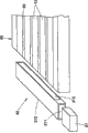
Fig. 3 is that existing another kind has utilized surface plasma resonance analysis of phenomenon device, has used and form the many optical waveguides 33 that fibre core 32 forms in covering 31.On each fibre core 32, be provided with metallic film 34 with the form that contacts with each fibre core 32.And, on each metallic film 34, be fixed with different antibody, supply with measured matter at this, the p polarized light is imported in each fibre core 32, instrumentation utilizes surface plasma resonance to check measured matter from the spectrum of the light of fibre core 32 outgoing.
This analytical equipment has used optical waveguide to replace prism, therefore can be implemented in the miniaturization of the optical system of using in this surface plasma resonance analytical equipment.But in this device, once the inspection quantity that can carry out equates with the radical of fibre core 32, can not realize enough high-throughputs.
2000-No. 131237 communiques of [patent documentation 1] TOHKEMY
2001-No. 255267 communiques of [patent documentation 2] TOHKEMY
2002-No. 162346 communiques of [patent documentation 3] TOHKEMY
In recent years, can check by gene or protein gradually, realize the early detection of grasp, disease of the health status that each is individual and then specific aim treatment etc. the individual.But, when carrying out these genes in checking or protein analysis, need to use the device of large-scale and high price, for example utilized the analytical equipment of surface plasma resonance method, therefore mainly carry out this inspection or analysis at present in research institute, and, the universal platform number of device is also limited, does not reach extensively to popularize.Therefore, expect further popularizing of such analytical equipment in the future, but, need small-sized and cheap analytical equipment in the enterprising enforcement usefulness of consumer's level.It is desirable to, be preferably hand sizes or portable size that the individual can move.And, in employed devices such as hospital or public institution, need once to check device a large amount of samples, that handling capacity is high.
But in the above-mentioned conventional example 1~3, it is also very expensive to be large-scale plant, price, and handling capacity does not yet meet the demands.And then, also can't measure affinity and interaction, the equilibrium constant etc. of gene or protein etc. accurately.
Summary of the invention
The present invention proposes in view of above-mentioned technical task, and its purpose is, light analyzer spare and the light analytical equipment that can realize miniaturization and cost degradation, can significantly improve handling capacity by hyperchannelization are provided.And, light analyzer spare and the light analytical equipment that can measure affinity and interaction, the equilibrium constant etc. of gene or protein etc. accurately are provided.
Being characterized as of light analyzer spare of the present invention has: light source portion; Waveguide unit, it has many fibre cores, channeling conduct in fibre core when interreflection is from the light of described light source portion; Optical detection part, it is received in guiding in the fibre core of described waveguide unit and the light that comes; Switching part, it has the switching device that can switch between the detected state of measuring object thing and non-detection status, under the situation of having arranged a plurality of described switching devices along the length direction of described fibre core, overlap with described waveguide unit; And the measuring object configuring area, it is set in across the described switching part position relative with described waveguide unit.Here switching device can be independent to every fibre core, also can be to cross between the many fibre cores.
According to above-mentioned light analyzer spare, only in the switching device that will arrange along the fibre core corresponding, switch to detected state with the corresponding switching device in the described measuring point of measuring object configuring area with measuring point in the described measuring object configuring area, detect from described light source portion by described test section and to send and guiding in described fibre core, light by the switching device that is in detected state after the modulation of described measuring point, can detect the intensity variations and the fluorescence color of described measuring point thus.Then, by detecting intensity variations or fluorescence color, can instrumentation be positioned over the type and the amount of the measuring object thing of described measuring point, and, the intermolecular interaction of measuring object thing and the characteristic of affinity, the equilibrium constant etc. can be estimated.Particularly, if use gene or protein etc., then can be used as biochip and use as the measuring object thing.In addition, this light analyzer spare can be used to utilize the surface plasma resonance phenomenon, constitute the surface plasma resonance analytical equipment together based on the means (for example, analysis software or computer system) of the output of this light analyzer spare, type, amount or the characteristic of analytical review object (physical characteristics, chemical characteristic and biological characteristics etc.).
In light analyzer spare of the present invention, used waveguide unit (optical waveguide), with to the light channeling conduct, therefore with compare to the device of space emergent light, can realize high sensitivity, can improve the instrumentation precision.And,, therefore hyperchannelization is realized in the measuring point of measuring object configuring area owing to used the switching part that constitutes by switching device, compare with the mechanical scanning mode simultaneously, can realize switching at a high speed, can carry out instrumentation to multiple measuring object thing at short notice, significantly improve handling capacity.And then, by using waveguide unit and switching part, can realize the miniaturization of light analyzer spare, can also realize the cheap of cost by producing in batches.
In a kind of embodiment of light analyzer spare of the present invention, has the inspection substrate that is arranged in described measuring object configuring area, described inspection substrate has a plurality of streams that subject flows through, in each stream, be fixed with acceptor, it seems that from described inspection substrate described stream overlaps with the lap of described switching device with the intersection region and the described fibre core of described fibre core.In such embodiment, by in the stream of having fixed acceptor, flowing through subject, and observe along intensity variations or its time of stream and change, can the instrumentation acceptor and subject in the affinity of the part that comprises and intermolecular interaction, the equilibrium constant.
And, this embodiment has a plurality of streams, therefore at same stream internal fixation identical acceptor, at each stream internal fixation under the situation of mutually different acceptor, the affinity of instrumentation subject and multiple acceptor and intermolecular interaction, the equilibrium constant in the lump, raising handling capacity.In addition, at each stream internal fixation under the situation of identical acceptor, by in each stream, flowing through different subjects, can once check a plurality of subjects, can improve handling capacity.
And, in this embodiment, if in described stream, form metallic film, sessile receptor on this metallic film, then can utilize the measurement of surface plasma resonance, the problem of inactivation of detection error such in the time that fluoroscopic examination can being avoided, that cause because of fluorescence molecule and the living body molecule of following fluorescence molecule etc.
In the another kind of embodiment of light analyzer spare of the present invention, the mutually different a plurality of measuring object things of 2 dimension shape ground arrangements in described measuring object configuring area, described each measuring object thing be configured in described fibre core and described switching device each lap directly over.In such embodiment, a plurality of measuring object things of instrumentation 2 dimension shape ground arrangement at high speed, so the handling capacity during the instrumentation operation becomes very high.
In this another kind embodiment, if in described measuring object configuring area, form metallic film, fixation measuring object on this metallic film, then can utilize the measurement of surface plasma resonance, the problem of inactivation of detection error such in the time that fluoroscopic examination can being avoided, that cause because of fluorescence molecule and the living body molecule of following fluorescence molecule etc.
Described switching part in another embodiment of light analyzer spare of the present invention is configured to described switching device and contacts with described fibre core, under non-detection status, the light that guides in described fibre core is reflected by described switching device, under detected state, the described switching device of the light transmission that in described fibre core, guides.Thus, by switching device is made as through state, can make the light that in fibre core, guides import the measuring object thing, make the light after being modulated return fibre core,, can make light not be subjected to the influence of measuring object thing herein by switching device is made as reflective condition.
As this switching part, when using the anisotropic liquid crystal device of the refractive index utilized liquid crystal, can realize the high speed of switch speed, and realize cost cheap of switching part.
Light detection method of the present invention is used to utilize light analyzer spare of the present invention and the variation that detects light, it is characterized in that, measuring point in the described measuring object configuring area is positioned according to the mode that clips switching device between any one fibre core in described measuring point and described fibre core, only in the switching device that will arrange along fibre core, the switching device corresponding with the described measuring point of measuring object configuring area switches to detected state, wherein said fibre core be with described measuring object configuring area in the corresponding fibre core in measuring point, detect from described light source portion by described optical detection part and to send and in described fibre core, be directed, by the light after place, described measuring point is modulated behind the switching device that is in detected state.
According to light detection method of the present invention, under situation about measuring by light analyzer spare of the present invention, can only separate and obtain along in a plurality of measuring points that fibre core is arranged, the measurement result of specific measuring point.
In addition, the inscape of above explanation of the present invention can at random make up within the possible range.
Description of drawings
Fig. 1 is the approximate three-dimensional map of the existing analytical equipment of expression.
Fig. 2 is the skeleton diagram of the existing another kind of analytical equipment of expression.
Fig. 3 be the expression existing another utilized the stereographic map of surface plasma resonance analysis of phenomenon device.
Fig. 4 is the exploded perspective view of expression according to the structure of the light analyzer spare of embodiments of the invention 1.
Fig. 5 is the planimetric map of the light analyzer spare of embodiment 1.
Fig. 6 is the sectional view along the fibre core length direction of the light analyzer spare of embodiment 1.
Fig. 7 is the sectional view of longshore current road length direction of the optical device of embodiment 1.
Fig. 8 is the sectional view of the part of expression switching part.
Fig. 9 is the sectional view that the part of substrate is checked in expression.
Figure 10 is the skeleton diagram that expression is fixed on the acceptor in the stream.
Figure 11 is the block scheme that constitutes the arithmetic processing section of plasmon resonance analysis device of the present invention.
Figure 12 is the key diagram of the situation of expression when providing subject in the stream of checking substrate.
Figure 13 is the key diagram of the propagation of expression switch window light when closing, in the fibre core.
Figure 14 is that the expression switch window is opened, the key diagram of the propagation of light during binding partner, in the fibre core not on acceptor.
Figure 15 is that the expression switch window is opened, the key diagram of the propagation of light when being combined with part on acceptor, in the fibre core.
Figure 16 is the sequential chart of an example of the control method of expression switching part.
Figure 17 is the sequential chart of the another kind of control method of expression switching part.
Figure 18 is the figure of expression along the result of the variation of certain stream instrumentation signal intensity.
Figure 19 be illustrated in the affinity of ligands specific and acceptor and the little situation that interacts under, separate and the key diagram of the situation that combines again with another acceptor in downstream from this receptor with the part of receptors bind.
Figure 20 is the figure of an example with the instrumentation amount that extracts from this curve of expression intensity curves.
Figure 21 (a)~Figure 21 (f) is the key diagram of an example of the manufacture method of expression waveguide unit.
Figure 22 (a)~Figure 22 (c) is the then key diagram of the operation that is used for the waveguide unit manufacturing of the operation of Figure 21 (f) of expression.
Figure 23 (a)~Figure 23 (f) is the key diagram of an example of the expression manufacture method of checking substrate.
Figure 24 (a)~Figure 24 (e) is the figure of the another kind of manufacture method of explanation waveguide unit.
Figure 25 (a)~Figure 25 (f) is the figure of the another kind of manufacture method of explanation waveguide unit.
Figure 26 is the exploded perspective view of expression according to the structure of the light analyzer spare of embodiments of the invention 2.
Figure 27 is the planimetric map of the light analyzer spare of embodiment 2.
Figure 28 is the skeleton diagram of the structure of the expression stream inside of checking substrate.
Figure 29 (a) is that Figure 29 (b) is the sectional view along its flow path length direction along the sectional view of the stream orientation of switching part and inspection substrate.
Figure 30 is the skeleton diagram of the another kind configuration of the interior acceptor of the stream of explanation inspection substrate.
Figure 31 is the exploded perspective view of expression according to the structure of the light analyzer spare of embodiments of the invention 3.
Figure 32 is the sectional view of expression along the cross section of the orientation of fibre core in the light analyzer spare of embodiment 3 and stream.
Figure 33 is the sectional view of expression along the length direction of fibre core in the light analyzer spare of embodiment 3 and stream.
Figure 34 is the exploded perspective view of expression according to the structure of the light analyzer spare of embodiments of the invention 4.
Figure 35 is the planimetric map of position relation in the light analyzer spare of expression embodiment 4, between switch window and the fibre core.
Figure 36 is the exploded perspective view of expression according to the structure of the light analyzer spare of embodiments of the invention 5.
Figure 37 is the planimetric map that is used for illustrating the position relation between each one of light analyzer spare of embodiment 5.
Figure 38 is the stereographic map that the another kind of structure of substrate is checked in expression.
Figure 39 is the exploded perspective view of expression according to the structure of the light analyzer spare of embodiments of the invention 6.
Figure 40 is the exploded perspective view of the variation of explanation embodiment 6.
Figure 41 is the exploded perspective view of another variation of explanation embodiment 6.
Figure 42 is the exploded perspective view of expression according to the structure of the light analyzer spare of embodiments of the invention 7.
Figure 43 is the sectional view that the part of structure of the employed switching part of light analyzer spare of expression embodiment 7 disconnects.
Figure 44 is the planimetric map of expression according to the structure of the employed light source portion of the light analyzer spare of embodiments of the invention 8, waveguide unit and test section.
Figure 45 is the planimetric map of expression according to the structure of the employed light source portion of the light analyzer spare of embodiments of the invention 9, waveguide unit and test section.
Figure 46 is the exploded perspective view of the employed optical branch of embodiment 9 portion.
Figure 47 is the stereographic map of expression according to the structure of the employed light source portion of light analyzer spare of embodiments of the invention 10.
Figure 48 is the key diagram of effect of the employed modulation portion of light source portion of explanation embodiment 10.
Symbol description
42 light source portion; 43 waveguide units; 44 switching parts; 45 check substrate; 46 test sections; 47 light-emitting components; 49 photo detectors; 51 fibre cores; 52 switch windows; 58 black matrix area; 60 streams; 61 metallic films; 62 acceptors; 63 filter the acceptor of usefulness; 65 arithmetic processing section; 79 subjects; 80 non-specific parts; 81 ligands specifics; 112 inlets; 113 escape holes.
Embodiment
Below, describe embodiments of the invention with reference to the accompanying drawings in detail.But the embodiment shown in below the invention is not restricted to can carry out suitable design alteration according to its purposes and purpose or various situation.
[embodiment 1]
Surface plasma resonance analytical equipment of the present invention (light analytical equipment a kind of) mainly has: light analyzer spare (41); And arithmetic processing section (65), it is used for the output based on the light analyzer spare that has utilized the optical plasma resonance effect, the type of analytical review object and amount, characteristic etc.During the summary narration, in embodiments of the invention 1, light analyzer spare is made of light source portion (42), waveguide unit (43), switching part (44), inspection substrate (45) and test section (43).Waveguide unit has many fibre cores (51), channeling conduct in fibre core when interreflection is from the light of light source portion.A plurality of light-emitting components (47) of formation illuminating part are configured to relative with an end face of each fibre core, and a plurality of photo detectors (49) that constitute test section are configured to relative with another end face of each fibre core.Thus, go into to inject in the fibre core interreflection and guiding in fibre core from the light that light-emitting component sends.On the other hand, the light from the other end outgoing of fibre core is received by the photo detector of optical detection part.
Switching part overlaps on the waveguide unit.Switching part has the switch window (52 that can switch between the detected state of measuring object thing and non-detection status; Said switching device in claims), switch window has been arranged a plurality of along the length direction of fibre core, for example whole for clathrate be configured.And switching part disposes under switch window and situation that the fibre core on waveguide road contacts, and under non-detection status, the light that guides in fibre core is switched the window reflection, under detected state, and the light transmission switch window that in fibre core, guides.Such switching part for example is made of the anisotropic liquid crystal device of the refractive index of having utilized liquid crystal, for each switch window, can use and can select material that direct light is carried out total reflection or it is seen through.And, on position on the switching part, relative with waveguide unit, be set with the measuring object configuring area as face.Therefore, be the measuring point of non-detection status at switch window, guiding in fibre core and the light that comes is switched the window reflection is not had an effect with the measuring object configuring area.On the other hand, be the measuring point of detected state at switch window, guiding in fibre core and the light and the measuring object configuring area of the light transmission switch window that comes are had an effect, the light that is acted on returns in the fibre core once more, is finally received by optical detection part.
Check that substrate has a plurality of streams that subject flows through, in each stream, formed metallic film, on this metallic film, be fixed with acceptor.The inspection substrate is configured to, and from the direction perpendicular to the inspection substrate, each switch window is overlapping in the intersection region of stream and fibre core.On switching part, this inspection substrate is configured in the measuring object configuring area.Particularly preferred disposition is that to be fixed with the face of metallic film of acceptor consistent with the face of measuring object configuring area.In the stream of checking substrate, subject passes through from a direction the opposing party, if comprise ligands specific in subject, then ligands specific replenishes to acceptor.Thus, certain switch window at switching part is under the situation of detected state, in the measuring point corresponding with this switch window, light and measuring object thing (with the ligands specific of receptors bind) interact and light are modulated, therefore by optical detection part this is detected, can estimate type, amount or the characteristic etc. of measuring object thing.
Switching timing (switch window is made as opening successively or will be made as unlatching etc. simultaneously along the switch window of stream) of the type (identical acceptor or mutually different acceptor) of the acceptor of fixing according to each measuring point, the opening of switch window etc., described light analyzer spare can be considered various measuring methods.For example, in checking substrate, also can be at the identical acceptor of same stream internal fixation, at the mutually different acceptor of each stream internal fixation.In this case, can learn in the situation that combines on the direction on longshore current road, between each acceptor and the ligands specific, therefore can learn interactional variation along stream, the affinity of ligands specific and acceptor, interactional size can be estimated, reaction can be once estimated by in a plurality of streams, fixing different acceptors to a plurality of acceptors.
More than, the summary of the surface plasma resonance analytical equipment of embodiment 1 is illustrated, below this surface plasma resonance analytical equipment is specifically described.
Shown in Fig. 4~Fig. 7 is embodiments of the invention 1, is the light analyzer spare that constitutes the surface plasma resonance analytical equipment of the present invention that has utilized the surface plasma resonance phenomenon.Fig. 4 is the exploded perspective view of the structure of expression light analyzer spare 41, and Fig. 5 is the planimetric map of this light analyzer spare 41.In addition, Fig. 6 is the sectional view along the fibre core length direction of light analyzer spare 41, and Fig. 7 is the sectional view of the longshore current road length direction of light analyzer spare 41.Light analyzer spare 41 is made of light source portion 42, waveguide unit 43, switching part 44, inspection substrate 45 and test section 46.
The groove of many linearities is set in the tabular covering of making by the transparent resin or the glass of high index of refraction 50, is embedded in the big transparent resin of refractive index ratio covering 50, forms many fibre cores 51 in parallel to each other at this groove, thereby constituted waveguide unit 43.And each fibre core 51 is that identical cross-sectional shape and same cross-sectional are long-pending.Light source portion 42 and test section 46 are under each light-emitting component 47 situation relative with the end face of each fibre core 51 with each photo detector 49, dispose relatively with the both ends of waveguide unit 43.
Be tabular switching part 44 and have a plurality of switch windows 52 of arranging with 2 dimension shapes or clathrate, can independently each switch window 52 be switched to through state or the non-state that sees through by electric signal.As shown in Figure 5, switching part 44 is stacked as one at the upper layer of waveguide unit 43, each row switch window 52 be configured in waveguide unit 43 each fibre core 51 directly over.And a row switch window 52 of arranging on fibre core 51 is arbitrarily arranged according to a determining deviation.
As switching part 44, for example can use the liquid crystal device of following liquid crystal photic gate etc.: the refractive index that utilize the refractive index anisotropy of liquid crystal, the refractive index of liquid crystal layer changes, sees through the liquid crystal layer in the state when opening and when closing equates substantially with the refractive index of fibre core 51.Fig. 8 is the sectional view of the part of the such switching part 44 of expression.This switching part 44 has been enclosed liquid crystal layer 55 between side group plate 53 and the inboard substrate 54 outside, and the inner face of side group plate 53 is provided with transparency electrode 56 outside, is formed with transparent opening electrode 57 and black matrix area 58 at the inner face of inboard substrate 54.Each opening electrode 57 is split into clathrate by black matrix area 58, and each opening electrode 57 part becomes switch window 52.By controlling the on-off element of TFT set in the black matrix area 58 etc., can be switched on or switched off the voltage that between each opening electrode 57 and transparency electrode 56, applies.Black matrix area 58 is to be coated with the zone that does not make the blackwash that light passes through, except closing outside the element, also be provided with the wiring graph that is connected with on-off element etc.
The inboard substrate 54, opening electrode 57, transparency electrode 56 and the outside substrate 53 that constitute switching part 44 preferably constitute by having the refractive index materials that equates substantially with the fibre core 51 of waveguide unit 43.Liquid crystal layer 55 makes variations in refractive index by applying voltage, between transparency electrode 56 and opening electrode 57, do not apply under the voltage condition, the refractive index of the refractive index ratio fibre core 51 of liquid crystal layer 55 is little, after applying voltage, the refractive index of liquid crystal layer 55 become and equate substantially (also can in contrast) with the refractive index of fibre core 51.Therefore, switch window 52 is closed and is not applied under the voltage condition between transparency electrode 56 and opening electrode 57, when the light of propagating in fibre core 51 is incident to switch window 52, this light is switched window 52 total reflections, but open and between transparency electrode 56 and opening electrode 57, be applied with under the voltage condition at switch window 52, when the light of propagating in fibre core 51 is incident to switch window 52, this light transmission switch window 52.
Fig. 9 is the sectional view that the part of substrate 45 is checked in expression.Check that substrate 45 depression on the back up pad of being made by sheets of glass or transparent resin substrate etc. 59 is provided with the stream 60 of many parallel groove shapes, the metallic film 61 that forms Au film etc. on the whole in back up pad 59 in whole or each stream 60.Can also can when being carried out ester moulding, the back up pad of being made by transparent resin substrate 59 form stream 60 by forming stream 60 to carrying out etching above the back up pad 59 made by sheets of glass.The refractive index of this back up pad 59 is preferably with the refractive index of fibre core 51 and equates.Also can in the stream 60 of back up pad 59, form after the metallic film 61, by etching or grind the bottom surface attenuation make back up pad 59, the bottom surface of exposing metallic film 61 thus in the bottom surface of checking substrate 45.In each stream 60, on the metallic film 61, be fixed with the mutually different acceptor 62 of the type corresponding and filter the acceptor 63 of usefulness with purpose.Check that substrate 45 releasably sticks on the switching part 44 by mating oil, be configured to from directly under the state seen, the length direction of the length direction of stream 60 and fibre core 51 is vertical (though be not limited to vertically, to be preferably vertically.)。In addition, preferably by the cover 64 of glass cover etc. cover streams 60 above.
Figure 10 is the skeleton diagram of the expression stream 60 interior acceptors of being fixed 62,63.The zone in the outside of the switch window 52 of upstream-side-end in stream 60 and switching part 44 be fixed with specific part (below, be called ligands specific.) in addition part (below, be called non-specific part.) acceptor (the non specific filtering protein of filtration usefulness of combination, non-specific filtration protein) 63, the zone relative with each switch window 52 in its downstream is fixed with the acceptor (probe protein, probe protein) 62 that combines with ligands specific.
Figure 11 is the block scheme that constitutes the arithmetic processing section 65 of surface plasma resonance analytical equipment of the present invention.This arithmetic processing section 65 is made of microcomputer or IC etc. and realizes miniaturization.Arithmetic processing section 65 by light source portion driving circuit 66, switching part control circuit 67, receiving circuit 68, analog/digital (below, be designated as A/D.) change-over circuit 69, analysis portion 70, master control part 71, storage unit 72, input part interface 73 and efferent interface 74 constitutes.Light source portion driving circuit 66 is controlled to be according to certain power each light-emitting component 47 of light source portion 42 luminous.Switching part control circuit 67 is based on from the instruction of master control part 71, open control to each switch window 52 of switching part 44 successively according to predetermined order.Receiving circuit 68 receives from the simulating signal of each photo detector 49 output of test section 46, and A/D change-over circuit 69 is to pass to analysis portion 70 after the digital signal with this analog signal conversion.Master control part 71 is made of microcomputer etc., and each one is carried out Comprehensive Control.Storage unit 72 has the rewritable storage medium of hard disk etc., and the analysis that stores the type that is used to analyze subject or intensity curves etc. is with software etc.The input that connects keyboard 75 and mouse 76 etc. on input part interface 73 transmits to master control part 71 from input part interface 73 from the data of input with the analysis usefulness of equipment input with equipment or communication line, is kept in the storage unit 72.Analysis portion 70 is based on the data that receive from test section 46 by receiving circuit 68 and A/D change-over circuit 69, calculates the type of the ligands specific that comprises in the intensity curves of subject or the subject and amount etc.Be connected with the output equipment of monitor 77 or printer 78 etc. on efferent interface 74, the instrumentation result of the intensity curves that analysis portion 70 calculated etc. is presented at by efferent interface 74 on the picture of monitor 77, perhaps, and from printer 78 outputs.
Then, actual process of carrying out the analysis of subject is described.At first, multiple acceptor that preparation will be corresponding with purpose 62 and the acceptor 63 that filters usefulness are fixed on each stream 60 and the inspection substrate 45 that obtains, coating coupling oil below this checks substrate 45, aligned position and sticking on the switching part 44.When seeing this state from the top, as shown in Figure 5, each switch window 52 of switching part 44 all is positioned at the intersection region of each fibre core 51 and each stream 60, and corresponding intersection region is corresponding one by one with switch window 52.As shown in Figure 6, the light 48 that sends from each light-emitting component 47 of light source portion 42 in the fibre core from the surface feeding sputtering to the correspondence 51, carries out total reflection repeatedly, and propagates in fibre core 51 respectively on the interface of fibre core 51, from the other end outgoing of fibre core 51, each photo detector 49 of detected portion 46 receives.But the light of propagating in fibre core 51 is different from light shown in Figure 6 48 in fact sometimes, also can be by more than 52 total reflection of a switch window.
As shown in figure 12, when a side of each stream 60 of checking substrate 45 provided subject 79, subject 79 was in stream 60, from upstream side side flow downstream.Upstream side at stream 60 is fixed with the acceptor 63 that filters usefulness, therefore offers the non-specific part 80 (impurity) that comprises in the subject 79 of stream 60 and combines and remove from subject 79 with the acceptor 63 that filters usefulness.Place, fixed position at acceptor 62 provides the subject 79 of having removed non-specific part 80 substantially, and when ligands specific 81 arrived acceptor 62, ligands specific 81 combined with acceptor 62.
At certain switch window 52 is under the situation of closing, as shown in figure 13, the light of propagating in fibre core 51 is in this switch window 52, by the interface total reflection of fibre core 51, therefore the not influence of the state of acceptor 62 of signal of propagating in fibre core 51, the light intensity of propagating in fibre core 51 does not change.
With respect to this, under the situation of certain switch window 52 for unlatching, as Figure 14 and shown in Figure 15, this switch window 52 of light transmission of in fibre core 51, propagating, 61 reflections of the metallic film of inspection substrate 45, the light that is reflected by metallic film 61 is subjected to the influence of surface plasma resonance phenomenon, test section 46 detected light intensities change (below, the variable quantity of this light intensity is called signal intensity.)。But, not being combined with on the acceptor 62 under the situation of ligands specific 81 as shown in Figure 14, the variation of the signal intensity that the surface plasma resonance phenomenon is caused is little.With respect to this, be combined with on the acceptor 62 under the situation of ligands specific 81 as shown in Figure 15, it is big that the variation of the signal intensity that the surface plasma resonance phenomenon is caused becomes.Particularly, the switch window 52 of light 48 by being in opening, by more than 61 reflection of metallic film, so light 48 is exaggerated and can detects big variation.Perhaps, the deviation that has or not of the combination in can the equalization zone can realize stable detection.
Thereby, if open switch window 52 successively along stream 60, then can be in each stream 60, detect along the variation of the signal intensity of the direction of stream 60.As the typical module of the switch window 52 of opening longshore current road 60 successively, pattern shown in Figure 16 and pattern shown in Figure 17 are arranged.
To the m root fibre core 51 that is arranged in parallel put on M=1,2,3 ..., the sequence number of m, to the n bar stream of arranging 60 perpendicularly put on N=1,2,3 ..., the sequence number of n, if by (M, N) switch window 52 (with reference to Fig. 5) at the intersection point place of expression between the stream 60 of the fibre core 51 of sequence number M and sequence number N.Mode shown in Figure 16 is, to the switch window 52 of M=1~m of on the direction parallel, arranging with stream 60 open simultaneously, closing control, and the row N of the switch window of opening 52 switches to the length direction of fibre core 51 successively.According to this method, can the instrumentation data be sent to receiving circuit 68 from test section 46 as parallel data by the signal intensity in each photo detector 49 each stream 60 of detection.
Mode shown in Figure 17 is, opens switch window 52 singly and scans the open site of each switch window 52.According to this method, can the instrumentation data be sent to receiving circuit 68 from test section 46 as serial data by the signal intensity in each photo detector 49 each stream 60 of detection.
Figure 18 is the figure of expression along the result of the variation of aforesaid stream 60 instrumentation signal intensities.As shown in figure 12, near the injection phase of subject 79, be fixed with the acceptor 63 that filters usefulness, non-specific part 80 is captured herein, therefore in Figure 18, near the spike of the signal intensity that appearance is caused by non-specific part 80 injection phase of subject 79 (in fact, there is not switch window 52 herein, so signal intensity does not herein observe.)。Because non-specific part 80 is captured herein,, be difficult in the signal intensity that stack is caused by non-specific part 80 on the signal intensity in the zone of acceptor 62 so be difficult to arrive the zone of having fixed acceptor 62.Therefore, can separate the signal intensity that signal intensity that non-specific part 80 caused and ligands specific 81 are caused, can reduce the flase drop of ligands specific 81, can improve accuracy of detection.
Under the affinity (affinity) between ligands specific 81 and the acceptor 62 and the big situation that interacts, the ligands specific 81 that arrival is fixed with the zone of acceptor 62 combines with acceptor 62 immediately, therefore as the intensity curves of representing with heavy line among Figure 18, the spike that is caused by ligands specific 81 is shown near a side of the injection phase of subject 79.With respect to this, under the affinity between ligands specific 81 and the acceptor 62 and the little situation that interacts, the ligands specific 81 that arrival is fixed with the zone of acceptor 62 moves in this zone and combines with acceptor 62 gradually, therefore as the intensity curves of representing with fine dotted line among Figure 18, the spike that is caused by ligands specific 81 is to the side shifting away from the injection phase of subject 79, and spike becomes gently (in other words, the height step-down of spike, the amplitude of spike broadens).
And, under the affinity between ligands specific 81 and the acceptor 62 and the little situation that interacts, as shown in figure 19, temporarily separate with acceptor 62 easily with the ligands specific 81 of acceptor 62 combinations, ligands specific 81 after the separation flows in stream 60, combines with other acceptor 62 once more.Therefore, when observation changed along time of the signal curve of stream 60, under the affinity and the big situation that interacts of ligands specific 81 and acceptor 62, intensity curves when having passed through the time, change still less, and under the affinity and the little situation that interacts, during effluxion, the peak location of intensity curves is side shifting downstream, and the affinity and the translational speed more little, spike that interacts are big more.And the intensity curves of the state that can stop according to variation is obtained the equilibrium constant.
In addition, in the past, though the decline rate of the signal intensity when ascending velocity by the signal intensity of observation part during with receptors bind or part separate with acceptor can the instrumentation part and the affinity and the interaction of acceptor, can't obtain enough accuracy.
As above explanation is such, and the surface plasma resonance analytical equipment of embodiments of the invention 1 is made of light analyzer spare 41 and arithmetic processing section 65.According to this surface plasma resonance analytical equipment, can be according to the variation (dynamic perfromance) of the shape of the shape (static characteristics) of the intensity curves on the direction of stream 60 and intensity curves, estimate the affinity and the interactional size of ligands specific 81 and acceptor 62.Particularly, as shown in figure 20, by the wide B of spike height H, half value of the intensity curves that causes by ligands specific 81, apart from the peak location L of subject injection phase and the translational speed V of spike etc., can carry out quantification to the affinity and the interaction of ligands specific 81.Therefore, can carry out affinity and interactional measurement, can analyze the affinity of part 81 and acceptor 62 or the interaction between protein accurately according to various physical quantitys.
And, in this surface plasma resonance analytical equipment, at a plurality of stream 60 internal fixation the mutually different acceptor 62 of type is arranged, therefore by in each stream 60, flowing through same subject 79, can measure simultaneously and the affinity and the interaction of certain specific ligands specific 81 of comparison and various acceptors 62.In addition, on the contrary,, then measure affinity and interaction that can a multiple ligands specific 81 of instrumentation by in each stream 60, flowing through the subject 79 that comprises different ligands specific 81 if having with receptoroid 62 at each stream 60 internal fixation.
In addition, in embodiment 1, also can in each stream 60, flow through the subject 79 that type has nothing in common with each other at the identical acceptor 62 of each stream 60 internal fixation.
And the area of the downside of the intensity curves that the amount of the ligands specific 81 that combines with acceptor 62 in the stream 60 and Figure 20 are such is directly proportional, and therefore by this area of calculating, can obtain the binding capacity between ligands specific 81 and each acceptor 62.And, because the acceptor 62 of each stream 60 is different, so, can determine the type of ligands specific 81 by comparing signal intensity from each acceptor 62.
And,,, make 41 miniaturizations of light analyzer spare by using optical waveguide (waveguide unit 43), light being propagated to test section 46 from light source portion 42 according to the present invention.And, by the switching part 44 of having arranged switch window 52 is set on waveguide unit 43, can the instrumentation gene or protein between affinity and interaction.Therefore, can make the miniaturization of surface plasma resonance analytical equipment, manufacturing cost is reduced.
Then, described light analyzer spare 41 employed waveguide units 43 and the manufacture method of checking substrate 45 are described.Figure 21 is the key diagram of an example of the manufacture method of expression waveguide unit 43.In this manufacture method, the at first plasma etching method by photoetching process, DRIE (Deep Reactive Ion Etching, deep reactive ion etch method) etc., laser processing method, cutting method etc., the mother matrix 82 (Figure 21 (a)) of making covering.Then,, make pressing mold 83 (Figure 21 (b)), peel off pressing mold 83 (Figure 21 (c)) from mother matrix 82 by electrocasting nickel deposited alloy etc. on mother matrix 82.Afterwards, the uv-hardening resin 85 that drips on parent glass 84 (Figure 21 (d)) is pushed uv-hardening resin 85 by pressing mold 83, spreads uv-hardening resin 85 out between parent glass 84 and pressing mold 83.And then, make its sclerosis (Figure 21 (e)) by parent glass 84 to uv-hardening resin 85 irradiation ultraviolet radiations, obtain covering 50 (Figure 21 (f)) by peeling off pressing mold 83.
Then, the fibre core resin 86 (Figure 22 (a)) of the uv-hardening resin that drips on covering 50 etc. is pushed fibre core resin 86 with pushing glass 87, and fibre core resin 86 is filled in the groove of covering 50.And then, by the ultraviolet ray irradiation etc., make 86 sclerosis of fibre core resin and fibre core 51 is shaped (Figure 22 (b)), peel off and push glass 87 and obtain waveguide unit 43 (Figure 22 (c)).In addition, parent glass 84 also can directly remain in covering 50 below.
Figure 23 is the key diagram of an example of the expression manufacture method of checking substrate 45, and is the same with waveguide unit 43, makes of compression moulding.That is, the plasma etching method by photoetching process, DRIE etc., laser processing method, cutting method etc. are made the mother matrix 88 (Figure 23 (a)) of back up pad 59.Then, by electrocasting nickel deposited alloy etc. on mother matrix 88, make pressing mold 89 (Figure 23 (b)).Afterwards, uv-hardening resin 91 drips on parent glass 90, push uv-hardening resin 91 by pressing mold 89, between parent glass 90 and pressing mold 89, spread uv-hardening resin 91 out, make its sclerosis (Figure 23 (c)) by parent glass 90 to uv-hardening resin 91 irradiation ultraviolet radiations, by peeling off the back up pad 59 (Figure 23 (d)) that pressing mold 89 obtains having stream 60.
Then, by vacuum evaporation etc., on stream 60 inner faces of back up pad 59 or back up pad 59 whole, form the metallic film 61 (Figure 23 (e)) of Au film etc., each stream 60 in, on metallic film 61, distinguish sessile receptor 62,63, obtain checking substrate 45 (Figure 23 (f)).In addition, check that the stream 60 of substrate 45 can be opened the top, but preferred as Figure 23 (f) shown in like that, overlapping lid glass on the back up pad 59 seal from the cover 64 that waits stream 60 above.
Figure 24 is the figure of the another kind of manufacture method of explanation waveguide unit 43.In the method, at first, painting erosion resistant agent 93 on glass substrate 92 (Figure 24 (a)).Make relative near resist 93 95 pairs of resists 93 of opening by exposed mask 94 expose (Figure 24 (b)) with it with the exposed mask 94 of the corresponding regional split shed in zone of the groove that becomes covering 50.Then,, remove exposed portion, on resist 93, leave window 96 (Figure 24 (c)) by the resist on the glass substrate 92 93 is developed.By this window 96 etchant is contacted with glass substrate 92, glass substrate 92 is carried out partially-etched, thereby on glass substrate 92, form many grooves 97 (Figure 24 (d)), obtain covering 50 (Figure 24 (e)) by the resist of peeling off on the glass substrate 92 93.Produce like this after the covering 50, by with the identical operation of operation of Figure 22 (a)~Figure 22 (c), be embedded in fibre core 51 and make waveguide unit 43 at the groove of covering 50.
Figure 25 is the figure that explanation and second kind of manufacture method of described waveguide unit 43 are similarly made the method for checking substrate 45.In the method, painting erosion resistant agent 99 (Figure 25 (a)) on glass substrate 98.Make relative near resist 99 101 pairs of resists 99 of opening by exposed mask 100 expose (Figure 25 (b)) with it with the exposed mask 100 of the corresponding regional split shed in zone that becomes stream 60.Then,, remove exposed portion, on resist 99, leave window 102 (Figure 25 (c)) by the resist on the glass substrate 98 99 is developed.By this window 102, etchant is contacted with glass substrate 98, glass substrate 98 is carried out partially-etched, thereby on glass substrate 98, form a plurality of streams 60 (Figure 25 (d)), obtain having the back up pad 59 (Figure 25 (e)) of stream 60 by the resist of peeling off on the glass substrate 98 99.Produce like this after the back up pad 59,, make and check substrate 45 (Figure 25 (f)) by on the inner face of stream 60 or back up pad 59 whole, forming metallic film 61.
[embodiment 2]
Then, light analyzer spare according to embodiments of the invention 2 is described.The structure of arithmetic processing section 65 is substantially the same manner as Example 1, therefore omits its explanation.
The light analyzer spare of embodiment 2 is characterised in that checks substrate 45.That is, in embodiment 2 employed inspection substrates 45, a plurality of streams are arranged in parallel to each other in the part relative with switching part 43, but each stream gathers inlet 112 an end, and the other end also gathers escape hole 113.According to this embodiment 2, can easily carry out the injection and the recovery of subject.
Figure 26 is the exploded perspective view of expression according to the structure of the light analyzer spare 111 of embodiments of the invention 2, and Figure 27 is its planimetric map.In embodiment 2, light source portion 42, waveguide unit 43, switching part 44 and test section 46 have the structure identical with embodiment 1.Be formed with a plurality of streams 60 in the inside of checking substrate 45, having on check substrate 45 to stream 60 provides the inlet 112 of subject 79 usefulness and will flow through the subject 79 that comes is discharged escape hole 113 from usefulness to the outside from stream 60.Branch into each stream 60 from inlet 112 by branching portion 114, at the opposition side of stream 60, each stream 60 merges into one by interflow portion 115 and is connected with escape hole 113.
When the top was seen, it is identical with embodiment 1 with the intersection region this point of fibre core 51 that stream 60 and fibre core 51 switch windows 52 vertical, switching part 44 are arranged in stream 60.
Figure 28 is the skeleton diagram of the inner structure of expression stream 60.Be fixed with the acceptor 63 that filters usefulness in position, be fixed with the mutually different acceptor 62 of type in the downstream of acceptor 63 near the inlet 112 of each stream 60.The density of the acceptor 62 of preferred each stream 60 equates.So the subject 79 that injects from inlet 112 flows into each stream 60 in branching portion 114 branches, by filtering acceptor 63 and each acceptor 62 of usefulness, flow in the interflow portion 115, discharge or be recovered to the outside from escape hole 113.Therefore,, can provide subject 79 to each stream 60 in the lump, simplify the analysis operation, improve handling capacity according to this embodiment.
In addition, the acceptor 63 of filtration usefulness also can be configured in by branching portion 114 and be divided on a plurality of streams 60 part (stream also is 1 a part) before.Thus, can suppress the deviation that the non-specific part between each stream 60 is removed.
Figure 29 (a) is the sectional view of switching part 44 and inspection substrate 45 (b), the cross section of the orientation on Figure 29 (a) expression longshore current road 60, the cross section of the length direction on Figure 29 (b) expression longshore current road 60.Check that substrate 45 mainly is made of cover 116 and back up pad 117.Cover 116 is made by resin forming product or glass that (material of cover 116 does not limit especially.), depression is provided with stream 60, branching portion 114 and interflow portion 115 below cover 116, at the end of branching portion 114 and the end difference sprue gated 112 and the escape hole 113 of interflow portion 115.Back up pad 117 is formed tabular or membranaceous by transparent resin or glass plate, by vacuum evaporation etc., be formed with the metallic film 61 of Au film etc. on back up pad 117.For back up pad 117, preferably use the material that equates of refractive index and fibre core 51.And on metallic film 61, in the position that becomes stream 60, predetermined fixed has acceptor 63 and each acceptor 62 (with reference to Figure 28) that filters usefulness.By under the situation below closure parts 116, with back up pad 117 be installed in cover 116 below make and check substrate 45, each acceptor 63,62 is accommodated in each stream 60.In addition, also can omit back up pad 117, only by metallic film 61 clog cover 116 below.Perhaps, can also be on switching part 44 formation metallic film 61, by switching part 44 clog cover 116 below.
The inspection substrate 45 that is made like this is placed on the switching part 44 across coupling oil.The acceptor 63 that filters usefulness this moment is positioned at the position that any one switch window 52 with switching part 44 all departs from, and acceptor 62 is configured to be across to the other end from an end of a row switch window 52.
Therefore, from said structure as can be known, by the surface plasma resonance analytical equipment of embodiment 2, the also affinity of instrumentation ligands specific and interaction accurately.And in embodiment 2, providing of subject 79 becomes simple, therefore further improved the ease of use of surface plasma resonance analytical equipment.
And such length that the acceptors of fix in the stream 60 62 needn't go out is as shown in figure 28 extended longways, also can be such as shown in figure 30, a stream 60 interior acceptors 62 are divided into a plurality of, and each acceptor 62 is configured in the position corresponding with each switch window 52.In the latter case, be preferably the density of the acceptor 62 in each acceptor 62 and area (that is, the quantity of acceptor 62) and equate (during the ratio of the quantity of known receptor, also can equate).
[embodiment 3]
Then, light analyzer spare according to embodiments of the invention 3 is described.The structure of arithmetic processing section 65 is substantially the same manner as Example 1, therefore omits its explanation.
The light analyzer spare of embodiment 3 be characterised in that the configuration of checking substrate 45 towards.That is, in embodiment 3 employed inspection substrates 45, parallel and each stream 60 of the stream of checking substrate 45 and the fibre core of waveguide unit 43 51 be positioned at each fibre core directly over situation under, be disposed on the switching part 44.Below, describe particularly.
Figure 31 is the exploded perspective view of the structure of the light analyzer spare 121 in the expression embodiments of the invention 3.Figure 32 is the sectional view along the cross section of the orientation of fibre core 51 and stream 60 of expression light analyzer spare 121, and Figure 33 is the sectional view along the cross section of the length direction of fibre core 51 and stream 60 of expression light analyzer spare 121.In embodiment 1 and embodiment 2, fibre core 51 vertical forms with the stream 60 of checking substrate 45 and waveguide unit 43 dispose, and in the light analyzer spare 121 of embodiment 3, dispose with the fibre core 51 parallel forms of the length direction of stream 60 and waveguide unit 43.
In embodiment 3, illustrated be with embodiment 2 in the same substrate of inspection substrate 45 of explanation, but also can be embodiment 1 employed inspection substrate 45.In this checked substrate 45, it was parallel with fibre core 51 to be configured to stream 60, such shown in Figure 32 and 33, each stream 60 across switch window 52 be positioned at each fibre core 51 directly over.Even stream 60 is parallel with fibre core 51 like this, also can be by opening switch window 52 successively along stream 60, the state that combines with acceptor 62 along stream 60 instrumentation ligands specifics, therefore can access along the intensity curves of stream 60 affinity that can the instrumentation ligands specific and the type of interaction or ligands specific, amount etc.
[embodiment 4]
Then, light analyzer spare according to embodiments of the invention 4 is described.The structure of arithmetic processing section 65 is substantially the same manner as Example 1, therefore omits its explanation.
The light analyzer spare of embodiment 4 is characterised in that the structure of switching part 43.That is, in embodiment 4 employed switching parts 43, a plurality of switch windows that are rectangle 52 are arranged along short side direction.Each switch window 52 is with the form configuration vertical with the length direction of stream 60, and the length on the long side direction of switch window 52 is longer than the length on the Width of stream 60 integral body.Below, describe particularly.
Figure 34 is the exploded perspective view of the structure of the light analyzer spare 131 in the expression embodiments of the invention 4.In the light analyzer spare 131 according to embodiment 4, each switch window 52 of switching part 44 is rectangle, and the length on the long side direction is longer than manying the width of a fibre core 51 integral body, is arranged with a plurality of on short side direction.And, check that the direction of the stream 60 of substrate 45 can be parallel with fibre core 51, also can be vertical with it.
In this light analyzer spare 131, switch window 52 is according to a determining deviation, only arrange in one direction, but as shown in figure 35, if the length direction of fibre core 51 is intersected (though be not limited to vertical with the long side direction of switch window 52, but be preferably vertical), then because the intersection region of fibre core 51 and switch window 52 is rectangular arrangement, so can take out oneself signal intensity of intersection region arbitrarily.Therefore, by the switch window of switch opening successively 52, can be implemented in the signal intensity removing method shown in Figure 16 of embodiment 1.And, by switching the switch window of opening 52 successively, simultaneously, taking out signal from photo detector 49 successively, timesharing ground takes out the signal intensity in each intersection region successively, can be implemented in signal intensity removing method illustrated in fig. 17 among the embodiment 1.Therefore, in such surface plasma resonance analytical equipment, the also type of interaction between analysing protein and affinity or ligands specific or amount etc. accurately.
[embodiment 5]
Then, light analyzer spare according to embodiments of the invention 5 is described.The light analyzer spare of embodiment 5 is characterised in that the measuring object configuring area or checks the structure of substrate 45.That is, in embodiment 5, in the measuring object configuring area, arranged mutually different a plurality of acceptor with two-dimentional shape, each acceptor be positioned at fibre core and switch window 52 each lap directly over, in this embodiment 5, check that substrate does not have stream.In conjunction with the embodiments, on the surface of the inspection substrate 45 that is equivalent to the measuring object configuring area, form metallic film 61, on metallic film 61 with 2 the dimension shapes arrange mutually different a plurality of acceptor, make each acceptor be positioned at fibre core and switch window 52 each lap directly over.Below, describe particularly.
Figure 36 is the exploded perspective view of the structure of the light analyzer spare 141 in the expression embodiments of the invention 5.Figure 37 is the planimetric map that is used to illustrate the position relation between each one of this light analyzer spare 141.Light analyzer spare 141 is made of light source portion 42, waveguide unit 43, switching part 44, inspection substrate 45 and test section 46.Light source portion 42 is made of a plurality of light-emitting components 47 of light emitting diode (LED) or lamp etc.Light source portion 42 can be made of a plurality of independently light-emitting components 47, also can use led array.Test section 46 is made of a plurality of photo detectors 49 of photodiode or phototransistor etc.Test section 46 can be made of a plurality of independently photo detectors 49 too, also can use photodetector array.
The groove of many linearities is set on the tabular covering of making by the transparent resin or the glass of high index of refraction 50, is embedded in the big transparent resin of refractive index ratio covering 50, form many fibre cores 51 parallel to each other, thereby constituted waveguide unit 43 at this groove.And each fibre core 51 is that identical cross-sectional shape and same cross-sectional are long-pending.Light source portion 42 and test section 46 are under each light-emitting component 47 situation relative with the end face of each fibre core 51 with each photo detector 49, dispose relatively with the both ends of waveguide unit 43.
Be tabular switching part 44 and have a plurality of switch windows 52 of arranging with 2 dimension shapes or clathrate, can independently each switch window 52 be switched to through state or the non-state that sees through by electric signal.Switching part 44 is stacked as one at the upper layer of waveguide unit 43, the switch window 52 of the row parallel with fibre core 51 be configured in waveguide unit 43 each fibre core 51 directly over.And a row switch window 52 of arranging on fibre core 51 is arbitrarily all arranged at a certain distance.Switching part 44 have with embodiment 1 in the identical structure (with reference to Fig. 8) of switching part 44 of explanation.
Check that substrate 45 forms by the metallic film 61 that forms Au film etc. on the roughly whole surface of the back up pad of being made by glass plate or transparent resin film 142, equally spaced is fixed with acceptor 62 in length and breadth on metallic film 61.Checking that acceptor 62 fixing on the substrate 45 all is dissimilar acceptor.Check that substrate 45 releasably sticks on the switching part 44 across coupling oil.
Checking that acceptor 62 fixing on the substrate 45 can separate one by one.Figure 38 is the inspection substrate 45 that acceptor 62 is separated one by one by framework 143.This inspection substrate 45 is provided with framework 143, this framework 143 be on back up pad 142, form after the metallic film 61, on metallic film 61 photosensitive resin coating, photoresist be etched into clathrate and constitute by photoetching process by a plurality of rectangular-shaped spaces.If separate each acceptor 62 by framework 143 like this, then when when each acceptor 62 provides subject 79, the subject 79 that provides to each acceptor 62 does not mix each other, can improve the inspection precision.
And, this surface plasma resonance analytical equipment also similarly to Example 1, has arithmetic processing section 65 as shown in figure 11, by as Figure 16 or control the fibre core 51 of switching part 44 as shown in Figure 17, can detect the situation that combines between each acceptor 62 and the ligands specific or signal intensity (with reference to Figure 13~Figure 15).
So at mounting switching part 44 on the waveguide unit 43, placing under the state of checking substrate 45 on the switching part 44, as shown in Figure 37, the switch window 52 of switching part 44 is arranged on the fibre core 51, checks that the acceptor 62 of substrate 45 is positioned on each switch window 52.Therefore, each acceptors 62 different to type provide the subject 79 that comprises ligands specific 81, by successively the opening of switch window 52 being switched by photo detector 49 detection signal strength, can check in the lump and each acceptor 62 between reaction, type or amount that can the instrumentation ligands specific.For example, be that 100, switch window 52 are 100 * 100 if establish fibre core 51, then by this surface plasma resonance analytical equipment, can once analyze the reaction between subject 79 and the 10000 kind of acceptor 62, can significantly improve handling capacity.
[embodiment 6]
Then, light analyzer spare according to embodiments of the invention 6 is described.The structure of arithmetic processing section 65 is substantially the same manner as Example 1, therefore omits its explanation.The light analyzer spare of embodiment 6 is characterised in that checks substrate 45.That is, identical at the employed inspection substrate of embodiment 6 45 itself with the inspection substrate 45 of embodiment 2, but the whole difference of the type that is characterized as the acceptor 62 of arrangement a stream 60 in.Below, describe particularly.
Figure 39 is the exploded perspective view of the structure of the light analyzer spare 151 in the expression conventional example 6.In embodiment 6, used the inspection substrate 45 of the structure identical with the structure that goes out shown in Figure 30 of embodiment 2.But in Figure 30, stream 60 interior acceptors 62 all are same type, and the type of acceptor 62 is all different in the present embodiment, and the acceptor 62 that is positioned at same stream 60 is also all different.
So, in such surface plasma resonance analytical equipment, in stream 60, arranged the mutually different acceptor 62 of type, so subject 79 becomes easily to providing of each acceptor 62, further improved handling capacity.
[embodiment 7]
Then, light analyzer spare according to embodiments of the invention 7 is described.The light analyzer spare of embodiment 7 is characterised in that the structure of measuring object configuring area.That is, in embodiment 5, in the measuring object configuring area, arranged mutually different a plurality of acceptor with two-dimentional shape, each acceptor be positioned at fibre core and switch window 52 each lap directly over.And switching part 44 forms as one with inspection substrate 45, checks that substrate 45 does not have stream.In conjunction with the embodiments, the top of switching part 44 is the measuring object configuring area, formation metallic film 61 on switching part 44, on metallic film 61 with 2 the dimension shapes arrange mutually different a plurality of acceptor, make each acceptor be positioned at fibre core and switch window 52 each lap directly over.Below, describe particularly.
Figure 42 is the exploded perspective view of the structure of the light analyzer spare 181 among the expression embodiment 7.Figure 43 is the sectional view that the part of the structure of the switching part 44 of use in the expression light analyzer spare 181 disconnects.In embodiment 7, (that is, outside substrate 53 top) directly forms the metallic film 61 of Au film etc. on the switching part 44 of having arranged a plurality of switch windows 52, is fixed with the mutually different acceptor 62 of type on this metallic film 61.And, can omit the outside substrate 53 and the transparency electrode 56 of switching part 44, directly apply voltage by the top of metallic film 61 sealing liquid crystal layers 55 and by metallic film 61 and 57 pairs of liquid crystal layers 55 of opening electrode.
According to such embodiment, form the structure of one owing to switching part 44 can be formed switching part 44 with checking substrate 45, can simplified structure, reduce whole manufacturing cost.And, acceptor 62 directly is fixed on the switching part 44, so the location of acceptor 62 and switch window 52 becomes easy.
[embodiment 8]
Then, light analyzer spare according to embodiments of the invention 8 is described.The light analyzer spare of embodiment 8 is characterised in that the structure of light source portion 42 and test section 46.That is, embodiment 8 is characterized as, and disposes collector lens 191 respectively between each light-emitting component 47 of light source portion 42 and fibre core 51 end faces, and, between the photo detector 49 of test section 46 and fibre core 51 end faces, dispose collector lens 192 respectively.Below, describe particularly.
Figure 44 is the planimetric map of the structure of the employed light source portion 42 of light analyzer spare, waveguide unit 43 and test section 46 in the expression embodiments of the invention 8.In surface plasma resonance analytical equipment according to embodiment 8, between each light-emitting component 47 of light source portion 42 and fibre core 51 end faces, dispose collector lens 191 respectively, and, between the photo detector 49 of test section 46 and fibre core 51 end faces, dispose collector lens 192 respectively.
By collector lens 191 is set on light source portion 42 like this, can assemble the light that sends from light-emitting component 47 and go into to inject in the fibre core 51, therefore improve the utilization ratio of light.And, by collector lens 192 is set on test section 46, can assemble from the light of fibre core 51 outgoing to go into to inject the photo detector 49, therefore can improve the accuracy of detection of signal intensity.
[embodiment 9]
Then, light analyzer spare according to embodiments of the invention 9 is described.The light analyzer spare of embodiment 9 is characterised in that the structure of light source portion 42, has reduced the necessary number of light-emitting component 47.Below, describe particularly.
Figure 45 is the planimetric map of the structure of light source portion 42, waveguide unit 43 and test section 46 used in the light analyzer spare of expression according to embodiments of the invention 9.In embodiment 9, between light source portion 42 and waveguide unit 43, be inserted with optical branch portion 201.Go out as shown in figure 46 like that, optical branch portion 201 is made of optical waveguide, be embedded at under-clad layer 202 and be branched to a plurality of fibre core 203, by top covering 204 covered fibre core 203 above.The refractive index ratio under-clad layer 202 of fibre core 203 and the refractive index of top covering 204 are big.Light-emitting component 47 is relative with the end face of the non-branch side of fibre core 203, and the end face of the fibre core 51 of waveguide unit 43 each end face with branch's side of fibre core 203 respectively is relative.
According to such embodiment, the optical branch that can will send from a light-emitting component 47 by optical branch portion 201 and send into each fibre core 51 of waveguide unit 43, therefore can reduce the quantity of the light-emitting component 47 in the light source portion 42, the consumption electric power in the light source portion 42 can be suppressed, and then manufacturing cost can also be reduced.
And, in Figure 45, used 2 optical branch portions 201, if strengthen the degree of the branch of optical branch portion 201, then also can constitute by light source portion 42 and 1 optical branch portion 201 that a light-emitting component 47 constitutes.And, optical branch portion 201 and waveguide unit 43 one are constituted.And, at sensitive side, also can use to have the photo-coupler with spline structure with this optical branch portion, reduce the use number of photo detector 49.
[embodiment 10]
Then, light analyzer spare according to embodiments of the invention 10 is described.The light analyzer spare of embodiment 10 is characterised in that the structure of light source portion 42, has reduced the necessary number of light-emitting component 47.Below, describe particularly.
Figure 47 is the stereographic map of expression according to the structure of the employed light source portion 42 of the light analyzer spare of embodiments of the invention 10.This light source portion 42 is made of the polarizer 211 and the modulation portion 212 of a light-emitting component 47, polarizing filter etc.And as shown in figure 48, modulation portion 212 has the light guide portion 213 that is formed by big transparent resin of refractive index or glass in front, is arranged with a plurality of liquid crystal photic gates 214 at the back side of light guide portion 213, is provided with reflecting surface 215 at the back side of each liquid crystal photic gate 214.It is relative with fibre core 51 that modulation portion 212 is configured to each liquid crystal photic gate 214, and light-emitting component 47 is relative with the side of light guide portion 213 across polarizer 211.
So, when making light-emitting component 47 luminous, the light transmission polarizer 211 that sends from light-emitting component 47 and become linearly polarized light goes into to inject in the light guide portion 213 of modulation portion 212, the light that incides in the light guide portion 213 carries out total reflection repeatedly, and guiding in light guide portion 213.Liquid crystal photic gate 214 reflected light when closing, make light transmission during unlatching, therefore light reflection that in light guide portion 213, guides and the liquid crystal photic gate 214 that passes through closed condition, and when arriving the liquid crystal photic gate 214 of opening, in the incident feed liquor crystal light shutters 214, the face 215 that is reflected reflects, and sees through liquid crystal photic gate 214 and light guide portion 213 thus, from the positive outgoing of modulation portion 212.Go into to inject in the fibre core 51 of corresponding waveguide unit 43 propagation fibre core 51 in from the light of the positive outgoing of modulation portion 212.Thus, by liquid crystal photic gate 214 is switched to opening successively, the light that can use to each fibre core 51 incident instrumentation successively from modulation portion 212.
By using such light source, can suppress the consumption electric power of light source portion 42 and make light source portion 42 miniaturizations.
In addition, though not shown, also can constitute light source portion by light-emitting component and micro-reflector, by the angle of control micro-reflector, the photoconduction that will send from light-emitting component 47 is to each fibre core.
(other)
Light analyzer spare of the present invention, the light analytical equipment that is made of optical device and arithmetic processing section also can use in the light analytical equipment beyond the surface plasma resonance analytical equipment, when using these light analytical equipments to measure light signal from test portion, can estimate the having or not of target substance (gene, DNA etc.) in the test portion, amount, intermolecular interaction, affinity and the equilibrium constant etc.For example, under the situation of the light analytical equipment that constitutes the fluoroscopic examination type, when in the stream of the inspection substrate of having pasted dna probe (probe DNA) to high-density, flowing through the sample DNA with sign such as fluorchrome, complementary DNA combination.Thus, if detect the signal of checking the position on the substrate, then can estimate interactional having or not or degree between each dna probe and the sample DNA.If adopt this method, then can realize the measurement etc. of the discovery level of the affirmation that has or not of the determining of sequence in the gene, specific gene and specific gene.
As other purposes according to analytical approach of the present invention, can list SNP (singlenucleotide polymorphism, single nucleotide polytypism) analysis, throw to give path or the identification of the affirmation of state, intracellular ion concentration measurement, protein or the functional analysis etc. of experiment with the metabolism/absorption/drainage of the material of mouse.In addition, can also be used to differentiate the Gernral Check-up of individual health status or the inspection that the personal security uses etc. according to analytical approach of the present invention.
Claims (13)
1. light analyzer spare has:
Light source portion;
Waveguide unit, it has many fibre cores, channeling conduct in fibre core when interreflection is from the light of described light source portion;
Optical detection part, it is received in guiding in the fibre core of described waveguide unit and the light that comes;
Switching part, it has the switching device that can switch between the detected state of measuring object thing and non-detection status, under the situation of having arranged a plurality of described switching devices along the length direction of described fibre core, overlap with described waveguide unit; And
The measuring object configuring area, it is set in across the described switching part position relative with described waveguide unit as face.
2. light analyzer spare according to claim 1 is characterized in that,
Have the inspection substrate that is arranged in described measuring object configuring area,
Described inspection substrate has a plurality of streams that subject flows through, and is fixed with acceptor in each stream,
It seems that from described inspection substrate described stream overlaps mutually with the lap of described switching device with the intersection region and the described fibre core of described fibre core.
3. light analyzer spare according to claim 2 is characterized in that,
At same stream internal fixation identical acceptor is arranged, mutually different acceptor is arranged at each stream internal fixation.
4. light analyzer spare according to claim 2 is characterized in that,
In described stream, be formed with metallic film, on this metallic film, be fixed with acceptor.
5. light analyzer spare according to claim 1 is characterized in that,
In described measuring object configuring area, arranged mutually different a plurality of measuring object thing 2 dimension shapes,
Described each measuring object thing be disposed at described fibre core and described switching device each lap directly over.
6. light analyzer spare according to claim 5 is characterized in that,
In described measuring object configuring area, be formed with metallic film, on this metallic film, be fixed with the measuring object thing.
7. light analyzer spare according to claim 1 is characterized in that,
Described switching part is configured to described switching device and contacts with described fibre core, and under non-detection status, the light that guides in described fibre core is reflected by described switching device, under detected state, and the described switching device of the light transmission that in described fibre core, guides.
8. light analyzer spare according to claim 7 is characterized in that,
Described switching part is made of the anisotropic liquid crystal device of the refractive index of having utilized liquid crystal, can select to make the direct light total reflection or see through for each switching device.
9. light analytical equipment has:
Any one light analyzer spare in the claim 1~8; And
Be used for output, the type of analytical review object or the unit of amount, characteristic etc. based on this light analyzer spare.
10. surface plasma resonance analytical equipment has:
Claim 4 or 6 described light analyzer spares; And
Be used to utilize the surface plasma resonance phenomenon, based on the output of this light analyzer spare, the unit of the type of analytical review object, amount or characteristic.
11. used the biochip of any described light analyzer spare in the claim 1~8.
12. a light detection method is used to utilize the described light analyzer spare of claim 1 to detect the variation of light, it is characterized in that,
Measuring point in the described measuring object configuring area is positioned according to the mode that clips switching device between any one fibre core in described measuring point and described fibre core,
Only in the switching device that will arrange along fibre core, the switching device corresponding with the described measuring point of measuring object configuring area switch to detected state, wherein said fibre core be with described measuring object configuring area in the corresponding fibre core in measuring point,
By described optical detection part detect from described light source portion send and in described fibre core, be directed, by the light after described measuring point is modulated behind the switching device that is in detected state.
13. the analytical approach of a measuring object thing is used the described light detection method of claim 12, estimates type, amount or the characteristic of measuring object thing.
Applications Claiming Priority (2)
| Application Number | Priority Date | Filing Date | Title |
|---|---|---|---|
| JP409456/2003 | 2003-12-08 | ||
| JP2003409456 | 2003-12-08 |
Publications (2)
| Publication Number | Publication Date |
|---|---|
| CN1890553A CN1890553A (en) | 2007-01-03 |
| CN100538331C true CN100538331C (en) | 2009-09-09 |
Family
ID=34650412
Family Applications (1)
| Application Number | Title | Priority Date | Filing Date |
|---|---|---|---|
| CNB2004800363866A Expired - Fee Related CN100538331C (en) | 2003-12-08 | 2004-12-08 | Light analytical equipment and light analyzer spare |
Country Status (5)
| Country | Link |
|---|---|
| US (1) | US7342663B2 (en) |
| EP (1) | EP1701151A4 (en) |
| JP (1) | JPWO2005054826A1 (en) |
| CN (1) | CN100538331C (en) |
| WO (1) | WO2005054826A1 (en) |
Families Citing this family (30)
| Publication number | Priority date | Publication date | Assignee | Title |
|---|---|---|---|---|
| JP2006226921A (en) * | 2005-02-18 | 2006-08-31 | Fuji Photo Film Co Ltd | Surface plasmon resonance measuring method |
| US7569382B2 (en) * | 2005-10-05 | 2009-08-04 | Instantlabs Medical Diagnostic Corp. | Disposable reactor module and detection system |
| JP4793753B2 (en) * | 2006-01-31 | 2011-10-12 | 新潟県 | Intermolecular interaction analyzer |
| JP4893032B2 (en) * | 2006-03-15 | 2012-03-07 | オムロン株式会社 | Optical component, optical sensor and surface plasmon sensor |
| WO2008075578A1 (en) * | 2006-12-19 | 2008-06-26 | Omron Corporation | Surface plasmon sensor |
| JP5397577B2 (en) * | 2007-03-05 | 2014-01-22 | オムロン株式会社 | Surface plasmon resonance sensor and chip for the sensor |
| JP2008233691A (en) * | 2007-03-22 | 2008-10-02 | Nikon Corp | Display device and optical device |
| US20110074054A1 (en) * | 2008-06-04 | 2011-03-31 | Kozo Tajiri | Process for producing an optical waveguide and stamp for use in the production process |
| US8564781B2 (en) | 2008-09-01 | 2013-10-22 | Hitachi Chemical Company, Ltd. | SPR sensor |
| JP2010096645A (en) * | 2008-10-17 | 2010-04-30 | National Institute Of Advanced Industrial Science & Technology | Microplate having periodic structure, surface plasmon excitation enhanced fluorescence microscope using the same, fluorescence microplate reader, and method of detecting specific antigen/antibody reaction |
| JP5219899B2 (en) * | 2009-03-26 | 2013-06-26 | 浜松ホトニクス株式会社 | Light irradiation device and light measurement device |
| KR101630897B1 (en) * | 2009-03-26 | 2016-06-15 | 하마마츠 포토닉스 가부시키가이샤 | Light irradiation device and light measurement device |
| JP5219898B2 (en) * | 2009-03-26 | 2013-06-26 | 浜松ホトニクス株式会社 | Light irradiation device and light measurement device |
| JP5585138B2 (en) * | 2010-03-17 | 2014-09-10 | オムロン株式会社 | Channel tip and jig |
| EP2607888B1 (en) | 2010-08-17 | 2022-01-12 | Konica Minolta Holdings, Inc. | Spfs sensor equipped with non-specific adsorption type purification mechanism |
| US8503848B2 (en) * | 2011-01-27 | 2013-08-06 | Hewlett-Packard Development Company, L.P. | Waveguide arrays |
| JP2012215473A (en) * | 2011-03-31 | 2012-11-08 | Fujifilm Corp | Analyzer and analysis chip, and temperature measurement method in analyzer |
| TWI481849B (en) * | 2011-05-24 | 2015-04-21 | Portable detection device | |
| CN102519908B (en) * | 2011-12-12 | 2013-08-14 | 天津大学 | Imaging optical microfluid sensing device and method thereof |
| JP5895504B2 (en) * | 2011-12-15 | 2016-03-30 | ソニー株式会社 | Imaging panel and imaging processing system |
| JPWO2014007134A1 (en) * | 2012-07-05 | 2016-06-02 | コニカミノルタ株式会社 | Sensor chip |
| JP5314205B2 (en) * | 2013-03-05 | 2013-10-16 | 浜松ホトニクス株式会社 | Light measuring device |
| JP5314204B2 (en) * | 2013-03-05 | 2013-10-16 | 浜松ホトニクス株式会社 | Light measuring device |
| CN105051523B (en) * | 2013-03-29 | 2019-02-01 | 索尼公司 | Data processing equipment, Systems for optical inspection, data processing method and data processor |
| EP2916125A1 (en) * | 2014-03-07 | 2015-09-09 | One Drop Diagnostics Sàrl | Fluorescence-detected assays on microfluidic chips |
| JP6301194B2 (en) | 2014-05-26 | 2018-03-28 | 浜松ホトニクス株式会社 | Optical plate, light irradiation device, light measurement device, light irradiation method, and light measurement method |
| US10408752B2 (en) * | 2016-10-18 | 2019-09-10 | National Taiwan University | Plasmonic sensor |
| JP6908470B2 (en) | 2017-08-25 | 2021-07-28 | 京セラ株式会社 | Electromagnetic wave detectors, programs, and electromagnetic wave detection systems |
| NL2020625B1 (en) * | 2017-12-22 | 2019-07-02 | Illumina Inc | Two-filter light detection devices and methods of manufacturing same |
| EP4045895A4 (en) * | 2019-10-15 | 2023-11-22 | LacriSciences, LLC | Multiplexed surface plasmon resonance sensing of analytes in liquid sample |
Family Cites Families (12)
| Publication number | Priority date | Publication date | Assignee | Title |
|---|---|---|---|---|
| JPH0933427A (en) | 1994-12-16 | 1997-02-07 | Toto Ltd | Biosensor and concentration measuring device therewith |
| US6432364B1 (en) * | 1998-07-06 | 2002-08-13 | Suzuki Motor Corporation | SPR sensor cell and immunoassay apparatus using the same |
| JP3761726B2 (en) | 1998-10-22 | 2006-03-29 | 富士写真フイルム株式会社 | Microarray chip reading method and reading apparatus |
| JP3579321B2 (en) | 2000-03-10 | 2004-10-20 | 財団法人神奈川科学技術アカデミー | Two-dimensional imaging surface plasmon resonance measurement apparatus and measurement method |
| US6529277B1 (en) * | 2000-07-07 | 2003-03-04 | California Institute Of Technology | Optical devices based on resonant configurational effects |
| JP2002148187A (en) * | 2000-11-08 | 2002-05-22 | Nippon Telegr & Teleph Corp <Ntt> | Optical waveguide type spr phenomenon measuring chip, manufacturing method for it and spr phenomenon measuring method |
| JP3576093B2 (en) | 2000-11-22 | 2004-10-13 | 日本電信電話株式会社 | Optical waveguide type SPR phenomenon measuring device |
| JP2003042947A (en) * | 2001-07-31 | 2003-02-13 | Mitsubishi Chemicals Corp | Surface plasmon resonance cell, and method of analyzing sample fluid using the same |
| JP2003065945A (en) | 2001-08-24 | 2003-03-05 | Aisin Seiki Co Ltd | Biochemical measuring instrument |
| US6707958B2 (en) * | 2001-11-20 | 2004-03-16 | Agilent Technologies, Inc. | Biochemical assay device using frustrated total internal reflection modulator with an imaging optical waveguide |
| JP2003287493A (en) * | 2002-03-27 | 2003-10-10 | Fuji Photo Film Co Ltd | Measuring apparatus |
| AU2003276870A1 (en) * | 2002-09-07 | 2004-03-29 | Lightwave Bioapplications | Bioanalysis systems including optical integrated circuit |
-
2004
- 2004-12-08 CN CNB2004800363866A patent/CN100538331C/en not_active Expired - Fee Related
- 2004-12-08 JP JP2005516030A patent/JPWO2005054826A1/en active Pending
- 2004-12-08 US US10/582,188 patent/US7342663B2/en not_active Expired - Fee Related
- 2004-12-08 WO PCT/JP2004/018315 patent/WO2005054826A1/en active Application Filing
- 2004-12-08 EP EP04819972A patent/EP1701151A4/en not_active Withdrawn
Also Published As
| Publication number | Publication date |
|---|---|
| US7342663B2 (en) | 2008-03-11 |
| US20070211254A1 (en) | 2007-09-13 |
| EP1701151A4 (en) | 2008-02-27 |
| EP1701151A1 (en) | 2006-09-13 |
| CN1890553A (en) | 2007-01-03 |
| JPWO2005054826A1 (en) | 2007-06-28 |
| WO2005054826A1 (en) | 2005-06-16 |
Similar Documents
| Publication | Publication Date | Title |
|---|---|---|
| CN100538331C (en) | Light analytical equipment and light analyzer spare | |
| CN101395462B (en) | Chip for surface plasma resonance sensor and surface plasma resonance sensor | |
| EP2092339B1 (en) | Microelectronic sensor device for detecting label particles | |
| CN101147049B (en) | Imaging method and apparatus | |
| US20110188030A1 (en) | Microelectronic sensor device for optical examinations in a sample medium | |
| EP2446249B1 (en) | Optical biosensor with focusing optics | |
| US20100320363A1 (en) | Optical sensor for measuring emission light from an analyte | |
| CN101278186A (en) | Biosensors with improved sensitivity | |
| JP2005134139A (en) | Optical waveguide sensor and measuring instrument using the same | |
| US11255790B2 (en) | Fluid detection panel with filter structure and fluid detection device with filter structure | |
| NL2003743A (en) | Method for detection of an analyte in a fluid sample. | |
| US20080019876A1 (en) | Sensing Apparatus with Noble Metal and Sensing System and Method Thereof | |
| US20030132406A1 (en) | Sensor element for optically detecting chemical or biochemical analytes | |
| FI128503B (en) | Sample plate and analyzing method | |
| WO2008075578A1 (en) | Surface plasmon sensor | |
| WO2008142492A1 (en) | Method for detecting label particles | |
| CN102985804A (en) | Cartridge with large-scale manufacturing design | |
| WO2009027896A1 (en) | Microelectronic sensor device with wetting detection | |
| JP2007509324A (en) | Multi-lens light assembly for diagnostic devices | |
| JP2004053372A (en) | Surface plasmon resonance apparatus and inspection cassette of the same | |
| US9134201B2 (en) | Fluid providing apparatus | |
| US20060252158A1 (en) | Sample recovery method and device | |
| EP1972927A1 (en) | Microelectronic sensor device for detecting label particles | |
| JP2004061222A (en) | Micro biochemical evaluation apparatus | |
| CN109612944B (en) | Spectrum detection system and spectrum detection analysis method |
Legal Events
| Date | Code | Title | Description |
|---|---|---|---|
| C06 | Publication | ||
| PB01 | Publication | ||
| C10 | Entry into substantive examination | ||
| SE01 | Entry into force of request for substantive examination | ||
| C14 | Grant of patent or utility model | ||
| GR01 | Patent grant | ||
| C17 | Cessation of patent right | ||
| CF01 | Termination of patent right due to non-payment of annual fee |
Granted publication date: 20090909 Termination date: 20111208 |