WO2025142183A1 - 表示装置 - Google Patents
表示装置 Download PDFInfo
- Publication number
- WO2025142183A1 WO2025142183A1 PCT/JP2024/040524 JP2024040524W WO2025142183A1 WO 2025142183 A1 WO2025142183 A1 WO 2025142183A1 JP 2024040524 W JP2024040524 W JP 2024040524W WO 2025142183 A1 WO2025142183 A1 WO 2025142183A1
- Authority
- WO
- WIPO (PCT)
- Prior art keywords
- display device
- layer
- transistor
- insulating layer
- disposed
- Prior art date
- Legal status (The legal status is an assumption and is not a legal conclusion. Google has not performed a legal analysis and makes no representation as to the accuracy of the status listed.)
- Pending
Links
Images













Classifications
-
- G—PHYSICS
- G02—OPTICS
- G02B—OPTICAL ELEMENTS, SYSTEMS OR APPARATUS
- G02B5/00—Optical elements other than lenses
- G02B5/20—Filters
-
- G—PHYSICS
- G09—EDUCATION; CRYPTOGRAPHY; DISPLAY; ADVERTISING; SEALS
- G09F—DISPLAYING; ADVERTISING; SIGNS; LABELS OR NAME-PLATES; SEALS
- G09F9/00—Indicating arrangements for variable information in which the information is built-up on a support by selection or combination of individual elements
- G09F9/30—Indicating arrangements for variable information in which the information is built-up on a support by selection or combination of individual elements in which the desired character or characters are formed by combining individual elements
-
- G—PHYSICS
- G09—EDUCATION; CRYPTOGRAPHY; DISPLAY; ADVERTISING; SEALS
- G09F—DISPLAYING; ADVERTISING; SIGNS; LABELS OR NAME-PLATES; SEALS
- G09F9/00—Indicating arrangements for variable information in which the information is built-up on a support by selection or combination of individual elements
- G09F9/30—Indicating arrangements for variable information in which the information is built-up on a support by selection or combination of individual elements in which the desired character or characters are formed by combining individual elements
- G09F9/33—Indicating arrangements for variable information in which the information is built-up on a support by selection or combination of individual elements in which the desired character or characters are formed by combining individual elements being semiconductor devices, e.g. diodes
-
- H—ELECTRICITY
- H10—SEMICONDUCTOR DEVICES; ELECTRIC SOLID-STATE DEVICES NOT OTHERWISE PROVIDED FOR
- H10D—INORGANIC ELECTRIC SEMICONDUCTOR DEVICES
- H10D30/00—Field-effect transistors [FET]
- H10D30/60—Insulated-gate field-effect transistors [IGFET]
- H10D30/67—Thin-film transistors [TFT]
-
- H—ELECTRICITY
- H10—SEMICONDUCTOR DEVICES; ELECTRIC SOLID-STATE DEVICES NOT OTHERWISE PROVIDED FOR
- H10D—INORGANIC ELECTRIC SEMICONDUCTOR DEVICES
- H10D86/00—Integrated devices formed in or on insulating or conducting substrates, e.g. formed in silicon-on-insulator [SOI] substrates or on stainless steel or glass substrates
- H10D86/40—Integrated devices formed in or on insulating or conducting substrates, e.g. formed in silicon-on-insulator [SOI] substrates or on stainless steel or glass substrates characterised by multiple TFTs
- H10D86/60—Integrated devices formed in or on insulating or conducting substrates, e.g. formed in silicon-on-insulator [SOI] substrates or on stainless steel or glass substrates characterised by multiple TFTs wherein the TFTs are in active matrices
-
- H—ELECTRICITY
- H10—SEMICONDUCTOR DEVICES; ELECTRIC SOLID-STATE DEVICES NOT OTHERWISE PROVIDED FOR
- H10H—INORGANIC LIGHT-EMITTING SEMICONDUCTOR DEVICES HAVING POTENTIAL BARRIERS
- H10H20/00—Individual inorganic light-emitting semiconductor devices having potential barriers, e.g. light-emitting diodes [LED]
-
- H—ELECTRICITY
- H10—SEMICONDUCTOR DEVICES; ELECTRIC SOLID-STATE DEVICES NOT OTHERWISE PROVIDED FOR
- H10H—INORGANIC LIGHT-EMITTING SEMICONDUCTOR DEVICES HAVING POTENTIAL BARRIERS
- H10H20/00—Individual inorganic light-emitting semiconductor devices having potential barriers, e.g. light-emitting diodes [LED]
- H10H20/80—Constructional details
- H10H20/85—Packages
- H10H20/851—Wavelength conversion means
-
- H—ELECTRICITY
- H10—SEMICONDUCTOR DEVICES; ELECTRIC SOLID-STATE DEVICES NOT OTHERWISE PROVIDED FOR
- H10H—INORGANIC LIGHT-EMITTING SEMICONDUCTOR DEVICES HAVING POTENTIAL BARRIERS
- H10H20/00—Individual inorganic light-emitting semiconductor devices having potential barriers, e.g. light-emitting diodes [LED]
- H10H20/80—Constructional details
- H10H20/85—Packages
- H10H20/852—Encapsulations
- H10H20/853—Encapsulations characterised by their shape
-
- H—ELECTRICITY
- H10—SEMICONDUCTOR DEVICES; ELECTRIC SOLID-STATE DEVICES NOT OTHERWISE PROVIDED FOR
- H10H—INORGANIC LIGHT-EMITTING SEMICONDUCTOR DEVICES HAVING POTENTIAL BARRIERS
- H10H20/00—Individual inorganic light-emitting semiconductor devices having potential barriers, e.g. light-emitting diodes [LED]
- H10H20/80—Constructional details
- H10H20/85—Packages
- H10H20/857—Interconnections, e.g. lead-frames, bond wires or solder balls
-
- H—ELECTRICITY
- H10—SEMICONDUCTOR DEVICES; ELECTRIC SOLID-STATE DEVICES NOT OTHERWISE PROVIDED FOR
- H10P—GENERIC PROCESSES OR APPARATUS FOR THE MANUFACTURE OR TREATMENT OF DEVICES COVERED BY CLASS H10
- H10P14/00—Formation of materials, e.g. in the shape of layers or pillars
- H10P14/20—Formation of materials, e.g. in the shape of layers or pillars of semiconductor materials
Definitions
- One embodiment of the present invention relates to a display device including a transistor using an oxide semiconductor and a light-emitting element using gallium nitride.
- the light-emitting elements are light-emitting diodes (LEDs) or micro-LEDs.
- the display device includes a sapphire substrate on which the light-emitting elements are formed and a backplane on which transistors containing oxide semiconductors or low-temperature polysilicon are formed, and a manufacturing method for the display device includes electrically connecting the light-emitting elements and the transistors by transferring the sapphire substrate to the backplane.
- the light-emitting elements of the display device manufactured in this manner can pass a current according to the potential supplied to the transistor. As a result, the light-emitting elements emit light, and the display device can display an image on the display section.
- Patent Documents 1 to 4 disclose display devices that include transistors and light-emitting elements.
- One of the objectives of the present invention is to provide a display device that includes a transistor using an oxide semiconductor and a light-emitting element using gallium nitride, and that can suppress a decrease in long-term reliability.
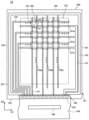
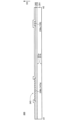
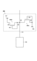
- FIG. 1 is a plan view showing a configuration of a display device according to a first embodiment of the present invention.
- 1 is a circuit diagram showing a circuit configuration of a pixel included in a display device according to a first embodiment of the present invention.
- 2 is a diagram showing a configuration of connections between the circuits of pixels and each wiring included in the display device according to the first embodiment of the present invention.
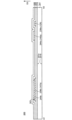
- FIG. FIG. 2 is a schematic plan view showing an example of a pixel layout according to the first embodiment of the present invention.
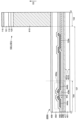
- 3A to 3C are cross-sectional views showing an example of a cross-sectional structure during a manufacturing process of the display device according to the first embodiment of the invention.
- 3A to 3C are cross-sectional views showing an example of a cross-sectional structure during a manufacturing process of the display device according to the first embodiment of the invention.
- 3A to 3C are cross-sectional views showing an example of a cross-sectional structure during a manufacturing process of the display device according to the first embodiment of the invention.
- 3A to 3C are cross-sectional views showing an example of a cross-sectional structure during a manufacturing process of the display device according to the first embodiment of the invention.
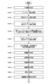
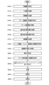
- 4 is a flowchart showing an example of a manufacturing method of the display device according to the first embodiment of the present invention.
- 3A to 3C are cross-sectional views showing an example of a cross-sectional structure during a manufacturing process of the display device according to the first embodiment of the invention.
- 3A to 3C are cross-sectional views showing an example of a cross-sectional structure during a manufacturing process of the display device according to the first embodiment of the invention.
- 3A to 3C are cross-sectional views showing an example of a cross-sectional structure during a manufacturing process of the display device according to the first embodiment of the invention.
- 3A to 3C are cross-sectional views showing an example of a cross-sectional structure during a manufacturing process of the display device according to the first embodiment of the invention.
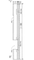
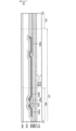
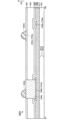
- 3A to 3C are plan views showing an example of a manufacturing process of the display device according to the first embodiment of the present invention.
- the second substrate 201 includes a first side 191, a second side 192 opposite the first side, a third side 193, and a fourth side 194 opposite the third side.
- the display area 122 and the peripheral area 121 are surrounded by the first side 191, the second side 192 opposite the first side, the third side 193, and the fourth side 194 opposite the third side 193.
- a plurality of pixels 180 are arranged in the display area 122.
- the display area 122 is an area that overlaps with the plurality of pixels 180 in a planar view.
- the plurality of pixels 180 are arranged in a matrix in the first direction D1 and the second direction D2.
- the arrangement of the plurality of pixels 180 is not limited to a matrix.
- the plurality of pixels 180 may be arranged in a staggered pattern.
- the pixel 180 includes a pixel IC chip 181, which will be described in detail later.
- the peripheral region 121 includes a plurality of scanning signal lines 129, a plurality of data signal lines 131, a ground wiring 145, a driving potential line 147, and a terminal region 126.
- the peripheral region 121 is a region that overlaps with the plurality of scanning signal lines 129, the plurality of data signal lines 131, the ground wiring 145, the driving potential line 147, and the terminal region 126 in a planar view.
- the plurality of scanning signal lines 129, the plurality of data signal lines 131, the ground wiring 145, and the driving potential line 147 are electrically connected to corresponding pixels 180 among the plurality of pixels 180.
- the terminal region 126 is an area on the third side 193 side.
- a plurality of terminals 150 are arranged in the terminal region 126.
- the plurality of terminals 150 are electrically connected to the FPC 108, the plurality of scanning signal lines 129, the plurality of data signal lines 131, the ground wiring 145, and the driving potential line 147.
- the terminal region 126 is an area that overlaps in a plan view with a plurality of terminals 150 for connecting the plurality of scanning signal lines 129, the plurality of data signal lines 131, the ground wiring 145, and the driving potential line 147 to the FPC 108, the driver IC 106, and an external circuit (not shown).
- the plurality of terminals 150 are included in the second substrate 201, and overlap with the FPC 108.
- the driver IC 106 is disposed on the FPC 108.
- the driver IC 106 supplies control signals for driving the pixels 180 to the pixels 180 via the FPC 108, the scanning signal lines 129, the data signal lines 131, the ground wiring 145, and the driving potential lines 147.
- the ground wiring 145 is arranged to surround the display area 122.
- the ground wiring 145 includes a wiring electrically connected to the terminal 150 on the first side 191 side and extending in the D1 direction along the third side 193, a wiring extending in the D2 direction along the first side 191, a wiring extending in the D1 direction along the fourth side 194, a wiring extending in the D2 direction along the second side 192, and a wiring electrically connected to the terminal 150 on the second side 192 side and extending in the D1 direction along the third side 193.
- the ground wiring 145 includes ground wirings 145a, 145b, and 145c that are electrically connected to the wiring extending in the D1 direction along the fourth side 194 and branched from the fourth side 194 side toward the third side 193 side along the D2 direction.
- constant potentials such as ground voltage, earth voltage, voltage VSS, and 0 V are supplied to the ground wiring 145.
- These voltages (potentials) are potentials that serve as references for each signal, and may be called reference voltages (potentials).
- the driving potential line 147 includes a wiring electrically connected to the terminal 150 on the first side 191 side and extending in the D1 direction along the third side 193, and a wiring extending in the D2 direction along the first side 191.
- the driving potential line 147 is also electrically connected to the wiring extending in the D2 direction along the first side 191, and includes driving potential lines 147a, 147b, and 147c branched from the first side 191 side toward the second side 192 side along the D1 direction.
- the driving potential lines 147a, 147b, and 147c are each electrically connected to a plurality of pixel IC chips 181 arranged along the D1 direction.
- a constant potential higher than the potential supplied to the ground wiring 145 is supplied to the driving potential line 147.
- the constant potential higher than the potential supplied to the ground wiring 145 is, for example, a voltage VDD, a potential of 30V, etc.
- the driving potential line 147 may be arranged to surround the display area 122, similar to the
- the ground wiring 145 including the configuration described above can uniformly supply a constant potential such as a ground voltage to the multiple pixel IC chips 181. Furthermore, the drive potential line 147 including the configuration described above can uniformly supply a constant potential such as a voltage VDD to the multiple pixel IC chips 181. As a result, the display device 10 can display an image without unevenness in the display area 122.
- the pixel 180 includes a pixel IC chip 181 electrically connected to the scanning signal line 129, the data signal line 131, the ground wiring 145, and the driving potential line 147.
- the pixel IC chip 181 includes a first transistor 184a, a second transistor 184b, a third transistor 184c, a light emitting diode 300, and a capacitance element 188.
- the pixel IC chip 181 also includes first connection conductive layers 244a, 244b, 244c, and 244d.
- the first connection conductive layers 244a, 244b, 244c, and 244d connect the corresponding electrodes and wiring using solder or an anisotropic conductive film (ACF).
- the first connection conductive layer 244a is arranged between and connects the gate electrode 3G, source electrode 3S, and cathode 6F to the ground wiring 145a
- the first connection conductive layer 244b is arranged between and connects the drain electrode 2D and second electrode 8S to the driving potential line 147a
- the first connection conductive layer 244c is arranged between and connects the gate electrode 1G and the scanning signal line 129
- the first connection conductive layer 244d is arranged between and connects the source electrode 1S and the data signal line 131.
- first connection conductive layer 244 In describing the first connection conductive layer included in pixel 180, if the first connection conductive layer is not differentiated, the first connection conductive layer is described as first connection conductive layer 244, and if the first connection conductive layer is differentiated, the first connection conductive layer is given an individual reference number such as first connection conductive layer 244a-244d.
- the first transistor 184a can function as a selection transistor.
- the conductive state of the first transistor 184a is controlled by the scanning signal line 129.
- the first transistor 184a includes a gate electrode 1G, a source electrode 1S, and a drain electrode 1D.
- the source electrode 1S is electrically connected to the data signal line 131
- the drain electrode 1D is electrically connected to the gate electrode 2G of the second transistor 184b and the first electrode 8F of the capacitance element 188
- the gate electrode 1G is electrically connected to the scanning signal line 129.
- the second transistor 184b can function as a drive transistor.
- the second transistor 184b controls the light emission brightness of the light emitting diode 300.
- the conduction state of the second transistor 184b is controlled by the first transistor 184a.
- the second transistor 184b includes a gate electrode 2G, a source electrode 2S, and a drain electrode 2D.
- the source electrode 2S is electrically connected to the drain electrode 3D of the third transistor 184c and the anode 6S of the light emitting diode 300
- the drain electrode 2D is electrically connected to the drive potential line 147 and the second electrode 8S of the capacitance element 188
- the gate electrode 2G is electrically connected to the drain electrode 1D and the first electrode 8F.
- the third transistor 184c can function as a protection circuit for the light-emitting diode 300.
- the third transistor 184c includes a gate electrode 3G, a source electrode 3S, and a drain electrode 3D.
- the third transistor 184c is connected in parallel to the light-emitting diode 300. More specifically, the source electrode 3S is electrically connected to the gate electrode 3G, the cathode 6F of the light-emitting diode 300, and the ground wiring 145, and the drain electrode 3D is electrically connected to the anode 6S and the source electrode 2S.
- the gate electrode 3G is electrically connected to the source electrode 3S, and the third transistor 184c is a diode including a so-called diode connection.
- the conduction state of the third transistor 184c is controlled by the potential difference between the potential supplied to the drain electrode 3D and the potential supplied to the source electrode 3S. Since the source electrode 3S is electrically connected to the ground wiring 145, the potential supplied to the drain electrode 3D is basically equal to or higher than the potential supplied to the ground wiring 145. When the potential supplied to the drain electrode 3D is lower than the potential supplied to the ground wiring 145, the third transistor 184c becomes conductive and functions as a protection circuit.
- the pixel 180 when an overvoltage is applied between the anode 6S and cathode 6F of the light-emitting diode 300, the pixel 180 (pixel circuit 182) can pass the current flowing through the light-emitting diode 300 to the ground wiring 145 via the third transistor 184c. As a result, the third transistor 184c can suppress the application of an overvoltage and the supply of an overcurrent to the light-emitting diode 300.
- transistor 184 When describing the transistors included in pixel 180, if the transistors are not to be distinguished, the transistors are described as transistor 184, and if the transistors are to be distinguished, the transistors are described as first transistor 184a, second transistor 184b, and third transistor 184c.
- the light-emitting diode 300 includes a cathode (n-type electrode) 6F and an anode (p-type electrode) 6S.
- Any control signal is supplied from the driver IC 106 and an external circuit to the pixel circuits 182 of the multiple pixels 180 of the display device 10, and the display device 10 can display an image in the display area 122.
- each electrode As a source and the function of the drain may be interchangeable.
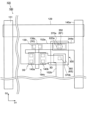
- FIG. 4 is a schematic plan view showing an example of the layout of the third transistor 184c and the light emitting diode 300. Configurations that are the same as or similar to those in Figs. 1 to 3 will be described as necessary.
- the n-type electrode 350 (cathode 6F) of the light-emitting diode 300 is connected to the second connection conductive layer 370a, the conductive layer 152a, and the conductive connection member 620a, and is connected to the first connection conductive layer 244a and the ground wiring 145a via the second connection conductive layer 370a, the conductive layer 152a, and the conductive connection member 620a.
- the n-type electrode 350 (cathode 6F) is connected to the gate electrode 138a (gate electrode 3G) exposed from the opening 139 and the source electrode 3S exposed from the opening 140a via the second connection conductive layer 370a and the conductive layer 152a.
- the p-type electrode 360 (anode 6S) of the light-emitting diode 300 is connected to the second connection conductive layer 370b and the conductive layer 152b, and is connected to the drain electrode 3D exposed from the opening 140b via the second connection conductive layer 370b and the conductive layer 152b.
- the third transistor 184c and the light-emitting diode 300 are provided on the same IC chip (pixel IC chip 181). As described in "1-2", the third transistor 184c functions as a protection circuit for the light-emitting diode 300.
- the display device 10 can have a configuration in which the light-emitting diode 300 and the third transistor 184c that protects the light-emitting diode 300 are integrally formed, rather than having the light-emitting diode 300 and the third transistor 184c that protects the light-emitting diode 300 individually.
- the electrical connection between the light-emitting diode 300 and the third transistor 184c can be stabilized more than if the light-emitting diode 300 and the third transistor 184c that protects the light-emitting diode 300 were individually provided. Therefore, the display device 10 can suppress the variation in the contact resistance between the light-emitting diode 300 and the third transistor 184c, and can stabilize the electrical characteristics of the light-emitting diode 300 and the third transistor 184c, thereby suppressing the deterioration of the light-emitting characteristics, temperature characteristics, etc. of the pixel 180.
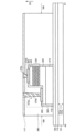
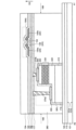
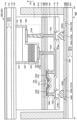
- FIG. 5 is a cross-sectional view showing an example of the cross-sectional structure of a pixel 180 of the display device 10. Specifically, it is a cross-sectional view showing an example of the cross-sectional structure of a pixel 180 cut along line A1-A2 shown in Fig. 1. Configurations that are the same as or similar to those in Figs. 1 to 4 will be described as necessary.
- the display device 10 includes an array substrate 100 and a backplane 200.
- the array substrate 100 includes a first substrate 101, an underlayer 110, a buffer layer 120, a light-emitting diode 300, an insulating layer 380, an insulating layer 117, an insulating layer 136, a second transistor 184b, an insulating layer 154, conductive layers 152a, 152b and 152c, an insulating layer 118, an insulating layer 119, openings 619a and 619b, and a color conversion layer 115.
- the backplane 200 includes a second substrate 201, an underlayer 210, a plurality of terminals 150 (see FIG. 1), conductive layers 238a and 238b, first connection conductive layers 244a and 244b, an insulating layer 240, and an insulating layer 246.
- the first substrate 101 is a substrate (first support substrate) that supports the transistor 184 and the light-emitting diode 300.
- the first substrate 101 includes a first surface 101a and a second surface 101b that faces the first surface 101a.
- the buffer layer 120, the light-emitting diode 300, the insulating layer 380, the insulating layer 117, the insulating layer 136, the second transistor 184b, the insulating layer 154, the conductive layers 152a, 152b, and 152c, the insulating layer 118, the insulating layer 119, and the openings 619a and 619b are disposed on the first surface 101a.
- the color conversion layer 115 is disposed on the second surface 101b.
- the underlayer 110 is disposed on the first substrate 101.
- the buffer layer 120 is disposed on the underlayer 110.
- the light-emitting diode 300 is disposed on the buffer layer 120.
- the light-emitting diode 300 includes a gallium nitride layer 310, an n-type semiconductor layer 320, a light-emitting layer 330, a p-type semiconductor layer 340, an n-type electrode 350, and a p-type electrode 360.
- the gallium nitride layer 310 is disposed on the buffer layer 120.
- the n-type semiconductor layer 320 is disposed on the gallium nitride layer 310.
- the light emitting layer 330 is disposed on the n-type semiconductor layer 320.
- the p-type semiconductor layer 340 is disposed on the light emitting layer 330.
- the n-type electrode 350 is disposed on the n-type semiconductor layer 320.
- the p-type electrode 360 is disposed on the p-type semiconductor layer 340.
- the insulating layer 116 is disposed so as to cover the light-emitting diode 300. Specifically, the insulating layer 116 is disposed on a portion of the surface of the buffer layer 120, the side surface of the gallium nitride layer 310, the side surface and a portion of the surface of the n-type semiconductor layer 320, the side surface of the light-emitting layer 330, and the side surface and a portion of the surface of the p-type semiconductor layer 340.
- the light-emitting diode 300 is a so-called micro LED or mini LED. However, the light-emitting diode 300 is not limited to the LED shown in the display device 10. The length of one side of a micro LED is 100 ⁇ m or less, and the length of one side of a mini LED is longer than 100 ⁇ m.
- the insulating layer 380 is disposed so as to cover a portion of the surface of the buffer layer 120, the light-emitting diode 300, and the insulating layer 116.
- the insulating layer 117 is disposed on the insulating layer 380.
- the insulating layer 380 may be referred to as a first planarization film.
- the second connection conductive layer 370a contacts the opening 372a (see FIG. 10) and the n-type electrode 350, and is electrically connected to the n-type electrode 350 via the opening 372a.
- the second connection conductive layer 370b contacts the opening 372b (see FIG. 10) and the p-type electrode 360, and is electrically connected to the p-type electrode 360 via the opening 372b. Since the openings 372a and 372b are formed in the insulating layers 117 and 380, the second connection conductive layer 370a contacts the insulating layers 117 and 380 that form the side walls of the opening 372a, and the second connection conductive layer 370b contacts the insulating layers 117 and 380 that form the side walls of the opening 372b.
- Insulating layer 136 is disposed on insulating layer 117. In addition, insulating layer 136 is disposed on the surfaces of second connecting conductive layers 370a and 370b. For example, insulating layer 136 is a base layer.
- the transistor 184 is disposed on the insulating layer 136.
- the transistor 184 includes a conductive layer 138, a gate insulating layer 140, an oxide semiconductor layer 142, a source electrode 144a, and a drain electrode 144b.
- the transistor 184 shown in FIG. 5 is, for example, a second transistor 184b.
- the conductive layer 138 is disposed on the insulating layer 136.
- the conductive layer 138 functions as a gate electrode.
- the conductive layer 138 shown in FIG. 5 is gate electrode 2G.
- the gate insulating layer 140 is disposed on the conductive layer 138 and on the surface of the insulating layer 136.
- the oxide semiconductor layer 142 is disposed on the gate insulating layer 140.
- the oxide semiconductor layer 142 is used for the channel of the transistor 184.
- the source electrode 144a and the drain electrode 144b are disposed on the oxide semiconductor layer 142 and on the gate insulating layer 140, spaced apart from each other.
- the source electrode 144a and the drain electrode 144b are electrically connected to the oxide semiconductor layer 142.
- the source electrode 144a and the drain electrode 144b of the display device 10 are directly connected to the oxide semiconductor layer 142.
- the source electrode, the drain electrode, and the wiring formed in the same layer as the source electrode and the drain electrode included in the pixel 180 when the source electrode, the drain electrode, and the wiring are not distinguished, the source electrode, the drain electrode, and the wiring are described as the conductive layer 144, and when the source electrode, the drain electrode, and the wiring are distinguished, the source electrode, the drain electrode, and the wiring are given individual reference characters such as the source electrode 144a, the drain electrode 144b, etc.
- the n-type semiconductor layer 320 includes a silicon-doped gallium nitride film formed in step S140. A portion of the surface of the n-type semiconductor layer 320 is etched and exposed.
- the light emitting layer 330 includes a laminated film formed in step S150 in which an indium gallium nitride film and a gallium nitride film are alternately laminated.
- the p-type semiconductor layer 340 includes a magnesium-doped gallium nitride film formed in step S160.
- a metal film such as palladium (Pd) or gold (Au) or a laminated metal film such as a metal film in which nickel (Ni) and gold (Au) are laminated is formed on a part of the p-type semiconductor layer 340 and on the insulating layer 116 by using sputtering, and a p-type electrode 360 is formed on the p-type semiconductor layer 340 by using photolithography and etching.
- the p-type electrode 360 includes a metal film such as palladium or gold or a laminated metal film such as a metal film in which nickel (Ni) and gold (Au) are laminated.
- the p-type electrode 360 is electrically connected to the p-type semiconductor layer 340.
- Step S200 is a step of forming an n-type electrode 350 on the n-type semiconductor layer 320.
- a specific example of step S200 is described below. Using photolithography and etching, a part of the insulating layer 116 is opened, and a part of the n-type semiconductor layer 320 is exposed.
- a metal film such as indium (In) or a laminated metal film such as a metal film in which titanium (Ti), aluminum titanium (AlTi) and gold (Au) are laminated is formed on a part of the n-type semiconductor layer 320 and on the insulating layer 116 using sputtering, and an n-type electrode 350 is formed on the n-type semiconductor layer 320 using photolithography and etching.
- the n-type electrode 350 includes a metal film such as indium or a laminated metal film such as a metal film in which titanium, aluminum titanium and gold are laminated.
- the n-type electrode 350 is electrically connected to the n-
- the n-type electrode 350 and the p-type electrode 360 are insulated from each other by the insulating layer 116. In other words, the n-type electrode 350 and the p-type electrode 360 are not short-circuited by the insulating layer 116.
- the light-emitting diode 300 is formed.
- Step S210 is a step of forming an insulating layer 380 so as to cover a part of the surface of the buffer layer 120, the light-emitting diode 300, and the insulating layer 116 (see FIG. 6 and FIG. 9).
- Step S210 is also a step of forming an insulating layer 117 on the insulating layer 380 (see FIG. 6 and FIG. 9).
- the insulating layer 380 is formed so as to cover a part of the surface of the buffer layer 120, the light-emitting diode 300, and the insulating layer 116 using an apparatus (coating apparatus) that coats a film on a substrate surface, and the insulating layer 117 is formed on the insulating layer 380 by sputtering.
- the insulating layer 380 and the insulating layer 117 are formed by photolithography and etching. As a result, a groove 189 is formed around each of the multiple light-emitting diodes 300. Although details will be described later, each of the multiple light-emitting diodes 300 can be divided into individual pieces by the groove 189. For example, a spin coater or a slit coater can be used as the coating apparatus.
- the insulating layer 380 can be an organic insulating film such as an acrylic resin film or a polyimide resin film. Since the insulating layer 380 includes an organic insulating film, it can flatten the unevenness caused by the light-emitting diode 300 and the insulating layer 116.
- the insulating layer 380 may be a single layer or a laminated layer. When the insulating layer 380 is a laminated layer, it may include not only an organic insulating film but also an inorganic insulating film such as a silicon oxide (SiOx) film or a silicon nitride (SiNx) film.
- the insulating layer 117 is formed using the same material as the insulating layer 116.
- the insulating layer 117 is formed using an aluminum oxide (AlO) film.
- AlO aluminum oxide
- the insulating layer 117 can prevent hydrogen, water, and the like from penetrating the insulating layer 380 and the transistor 184, and from diffusing hydrogen, water, and the like into the insulating layer 380 and the transistor 184.
- the refractive index of the insulating layer 117 is greater than the refractive index of silicon oxide (SiOx)
- the insulating layer 117 can reflect the light emitted from the light-emitting diode 300, like the insulating layer 116.
- the insulating layer 117 can suppress the fluctuation of the electrical characteristics of the transistor 184 based on the light emitted from the light-emitting diode 300.
- Step S220 is a step of forming openings 372b and 372a using photolithography and etching (see Figures 6 and 10). Opening 372a exposes insulating layers 117 and 380 that form the sidewalls of opening 372a, as well as a portion of the surface of n-type electrode 350. Opening 372b exposes insulating layers 117 and 380 that form the sidewalls of opening 372b, as well as a portion of the surface of p-type electrode 360.
- Step S230 is a step of depositing and forming the second connection conductive layers 370a and 370b (see FIG. 6 and FIG. 10).
- a conductive film is deposited by sputtering on the insulating layers 117 and 380 that form the side walls of the opening 372a, a portion of the surface of the n-type electrode 350, the insulating layers 117 and 380 that form the side walls of the opening 372b, and a portion of the surface of the p-type electrode 360.
- the second connection conductive layer 370a is formed on the insulating layers 117 and 380 that form the side walls of the opening 372a and a portion of the surface of the n-type electrode 350
- the second connection conductive layer 370b is formed on the insulating layers 117 and 380 that form the side walls of the opening 372b and a portion of the surface of the p-type electrode 360 by photolithography and etching.
- the conductive film includes the second connection conductive layers 370a and 370b.
- the conductive film may be a laminated metal film of aluminum and titanium (Al/Ti film).
- the second connection conductive layer 370a is electrically connected to the n-type electrode 350
- the second connection conductive layer 370b is electrically connected to the p-type electrode 360.
- Step S240 is a step of forming an insulating layer 136 on the surfaces of the insulating layer 117 and the second connecting conductive layers 370a and 370b so as to be in contact with the insulating layer 117 and the second connecting conductive layers 370a and 370b (see Figures 11 and 12).
- the insulating layer 136 can be formed in the same manner as the base layer 110 using the same material as the base layer 110.
- Step S250 is a step of forming a conductive layer 138 on the insulating layer 136 so as to be in contact with the insulating layer 136 by sputtering.
- the conductive layer 138 is formed using a metal film containing a common metal.
- the common metal is a metal film containing aluminum (Al), titanium (Ti), chromium (Cr), cobalt (Co), nickel (Ni), molybdenum (Mo), hafnium (Hf), tantalum (Ta), tungsten (W), bismuth (Bi), silver (Ag), copper (Cu), or an alloy or compound thereof.
- the conductive layer 138 may be a single layer or a multilayer.
- Step S270 is a step of depositing a gate insulating layer 140 by sputtering on the conductive layer 138 and on the surface of the insulating layer 136 so as to be in contact with the conductive layer 138 and the insulating layer 136.
- the gate insulating layer 140 may be made of silicon oxide (SiOx).
- Step S280 is a step of forming an oxide semiconductor layer 142 on the gate insulating layer 140 by sputtering so as to be in contact with the gate insulating layer 140.
- the oxide semiconductor layer 142 can be made of a metal oxide having semiconductor properties. Specifically, an oxide semiconductor containing indium, gallium (Ga), zinc (Zn) and oxygen (O), or an oxide semiconductor containing indium, tin (Sn), zinc and oxygen can be used. Note that the oxide semiconductor layer 142 may be amorphous or crystalline. The oxide semiconductor layer 142 may be both amorphous and crystalline.
- the conductive layer 144 includes a laminated structure of a layer containing titanium and a layer containing aluminum.
- the conductive layer 144 may include a three-layer structure (Ti/Al/Ti or TiN/Al/TiN, etc.) in which titanium or titanium nitride (TiN) and aluminum are laminated in order.
- the conductive layer 144 may also include a five-layer structure (TiN/Ti/Al/TiN/Ti, etc.) in which titanium or titanium nitride (TiN) and aluminum are laminated in order.
- the conductive layer 144 includes a laminated structure of layers using titanium or titanium nitride
- Titanium and titanium nitride have high hydrogen storage properties, and the conductive layer 144 functions as a protective film that protects the oxide semiconductor layer 142.
- the conductive layer 138 can absorb hydrogen discharged from the layer in contact with the conductive layer 138 during heat treatment in the manufacturing process of the display device 10, and can suppress the diffusion of hydrogen into the oxide semiconductor layer 142.
- Step S310 is a step in which the conductive layer 144 formed in step S300 is processed using photolithography and etching to form a source electrode, a drain electrode, and a wiring.
- the conductive layer 144 functions as a source electrode, a drain electrode, or a wiring.
- the conductive layer 144 shown in FIG. 12 is a source electrode 144a and a drain electrode 144b.
- the source electrode 144a and the drain electrode 144b are formed in the same layer and are disposed on the oxide semiconductor layer 142 and on a part of the gate insulating layer 140, spaced apart from each other.
- transistor 184 is formed.
- Step S320 is a step of forming an insulating layer 146 by sputtering on the conductive layer 144 and on a part of the gate insulating layer 140 so as to be in contact with the conductive layer 144 and the gate insulating layer 140, and forming an insulating layer 154 on the insulating layer 146 so as to be in contact with the insulating layer 146.
- the insulating layer 146 can be formed in the same manner as the gate insulating layer 140 using a material similar to that of the gate insulating layer 140.
- the insulating layer 154 can be formed in the same manner as the insulating layer 380 using a material similar to that of the insulating layer 380.
- the insulating layer 154 can flatten the unevenness due to the transistor 184 and the insulating layer 146, similar to the insulating layer 380.
- Step S330 is a step of forming openings 151a to 151d using photolithography and etching.
- Opening 151a exposes the insulating layer 136, gate insulating layer 140, insulating layers 146 and 154, which form the sidewalls of opening 151a, and a portion of the surface of second connecting conductive layer 370a.
- Opening 151b exposes the insulating layer 136, gate insulating layer 140, insulating layers 146 and 154, which form the sidewalls of opening 151b, and a portion of the surface of second connecting conductive layer 370b.
- Opening 151c exposes the insulating layers 146 and 154, which form the sidewalls of opening 151c, and a portion of the surface of drain electrode 144b.
- Opening 151d exposes the insulating layers 146 and 154, which form the sidewalls of opening 151d, and a portion of the surface of source electrode 144a.
- Step S340 is a step of depositing a conductive film and forming bumps.
- Conductive layers 152a to 152c include the conductive film, with conductive layers 152a and 152c functioning as bumps and conductive layer 152b functioning as wiring.
- step S340 uses sputtering and electrochemical plating (ECP) to deposit a conductive film on insulating layer 154, insulating layer 136 forming the sidewall of opening 151a, gate insulating layer 140, insulating layers 146 and 154, and part of the surface of second connection conductive layer 370a.
- ECP electrochemical plating
- the conductive film formed in step S340 can use a hydrogen storage metal.
- the hydrogen storage metal is copper, titanium, zirconium (Zr), zirconium (Zr), palladium (Pd), magnesium (Mg), manganese (Mn), or an alloy containing at least one of these metals.
- the conductive layer 152 contains a hydrogen storage metal.
- the conductive layer containing at least one of the hydrogen storage metals can use a conductive layer composed of manganese and copper.
- manganese oxide (MnO) is formed between the conductive layer 152 and the insulating layer in contact with the conductive layer 152.
- Step S410 is a step of depositing a conductive film on the underlayer 210 so as to be in contact with the underlayer 210 (see FIGS. 18 and 19).
- Step S420 is a step of processing the conductive film deposited in step S410 using photolithography and etching to form a plurality of scanning signal lines 129, driving potential lines 147, and wiring (see FIGS. 18 and 19).
- the conductive layers 238a and 238b shown in FIG. 19 include a conductive film, and the conductive layer 238a functions as the scanning signal line 129, and the conductive layer 238b functions as the driving potential line 147a.
- the conductive layers 238a and 238b can be deposited using the same material as the conductive layers 152a to 152c, and formed in the same manner.
- Step S430 is a step of depositing an insulating layer 240 by sputtering on the conductive layers 238a and 238b and on the surface of the underlayer 210 so as to be in contact with the conductive layers 238a and 238b and the underlayer 210 (see Figures 18 and 19).
- the insulating layer 240 can be formed in the same manner as the gate insulating layer 140 and the insulating layer 146, using the same material as the gate insulating layer 140 and the insulating layer 146.
- Step S440 is a step of forming an opening 243 using photolithography and etching (see Figures 18 and 19).
- the opening 243 exposes a part of the surface of the insulating layer 240 and the conductive layer 238b that will become the sidewall of the opening 243.
- Step S450 is a step of forming a conductive film so as to contact a part of the surface of the insulating layer 240 and the conductive layer 238b (see FIG. 18 and FIG. 20).
- Step S460 is a step of processing the conductive film formed in step S450 using photolithography and etching to form a plurality of data signal lines 131, ground wiring 145, the first connection conductive layer 244, and wiring (see FIG. 18 and FIG. 20).
- the first connection conductive layer 244a functions as the ground wiring 145a
- the first connection conductive layer 244b is electrically connected to the conductive layer 238b and functions as the drive potential line 147a.
- the first connection conductive layers 244c and 244d are formed in the same manner as the first connection conductive layers 244a and 244b by steps S450 and S460.
- the first connection conductive layer 244c (see FIG. 3) is electrically connected to the conductive layer 238a and functions as the scanning signal line 129.
- the first connection conductive layer 244d functions as the data signal line 131.
- the first connection conductive layer 244 can be formed in the same manner by depositing the same material as the conductive layers 238a and 238b and the conductive layers 152a to 152c.
- the first connection conductive layer 244c is electrically connected to the scanning signal line 129 via a conductive connection member 620 different from the conductive connection member 620a and the conductive connection member 620b.
- the conductive connection member 620 that electrically connects the first connection conductive layer 244c and the scanning signal line 129 may be called a conductor (third conductor).
- the backplane 200 is formed.
- Step S470 is a step in which the individualized pixel IC chips 181 are bonded to the backplane 200.
- Step S470 is a step of bonding the individualized pixel IC chips 181 and the backplane 200 (see Figures 18 and 21).
- An adhesive resin material 610 is formed on the buffer layer 120 using a coating device.
- the adhesive resin material 610 is also formed using photolithography and etching so as to surround at least a portion of the periphery of the light-emitting diode 300 and the transistor 184.
- conductive connection members 620a and 620b are formed on the first connection conductive layer 244 (here, the first connection conductive layers 244a and 244b).
- the conductive connection members 620a and 620b may be made of solder or anisotropic conductive film (ACF).
- the pixel IC chip 181 (the first surface 101a of the array substrate 100) is disposed so as to face the first surface 201a of the backplane 200, and the pixel IC chip 181 and the backplane 200 are bonded together by the adhesive resin material 610.
- the conductive connection members 620a and 620b contact the openings 619a and 619b and are electrically connected to the conductive layers 152a and 152c. That is, the conductive connection member 620a is electrically connected to the light-emitting diode 300 through the opening 619a, and the conductive connection member 620b is electrically connected to the transistor 184 through the opening 619b.
- the adhesive resin material 610 may be formed on the second substrate 201 instead of the first substrate 101, and the conductive connection members 620a and 620b may be formed on the conductive layers 152a and 152c instead of the first connection conductive layer 244.
- Steps S480 to S500 are steps for pressing the bonded pixel IC chip 181 and backplane 200 together and temporarily curing and fully curing the conductive connection member 620.
- the manufacturing method for the display device 10 includes steps S490 and S500, but the manufacturing method for the display device 10 may involve only fully curing the conductive connection member 620, without gradually curing and fully curing the conductive connection member 620 as in steps S490 and S500.
- the conductive layer 152a of the pixel IC chip 181 (array substrate 100) is electrically connected to the first connection conductive layer 244a of the backplane 200 via the conductive connection member 620a, and the conductive layer 152c of the pixel IC chip 181 (array substrate 100) is electrically connected to the first connection conductive layer 244b of the backplane 200 via the conductive connection member 620b.
- the manufacturing method of the display device 10 can electrically connect the pixel IC chip 181 (first surface 101a of the array substrate 100) to the backplane 200.
- the pixel IC chip 181 which includes the light-emitting diode 300 and the first to third transistors 184a to 184c, is electrically connected to the data signal line 131, the scanning signal line 129, the ground wiring 145, and the drive potential line 147 included in the backplane 200.
- the contact resistance value may vary depending on the bonding between the light-emitting diode chip and the transistor. Therefore, in a display device in which the light-emitting diode chip is transferred and connected to the transistor, there is a risk that the light-emitting characteristics and temperature characteristics of the pixel may deteriorate.
- the light-emitting diode 300 and the multiple transistors 184 for driving the light-emitting diode 300 of the display device 10 can be formed on the same first substrate 101.
- the light-emitting diode 300 and the pixel circuit 182 including the second transistor 184b for driving the light-emitting diode 300 are electrically connected on the same first substrate 101.
- the display device 10 can be completed as a display device in a state in which the contact resistance value between the light-emitting diode and the transistor is stabilized by transferring the pixel 180 including the light-emitting diode and the transistor for driving the light-emitting diode as a one-chip pixel IC chip 181 to the backplane. Because the current supplied to the light-emitting diode 300 by the second transistor 184b is stabilized, the display device 10 can suppress deterioration of the light-emitting characteristics and temperature characteristics of the pixel 180.
- the electrical characteristics of the light-emitting diode depend on the electrical characteristics of the multiple transistors. In other words, it is difficult to optimally adjust the electrical characteristics of the multiple transistors for driving the light-emitting diode and the light-emitting diode for each device.
- the multiple transistors 184 for driving the light-emitting diode 300 of the display device 10 are formed in a process different from that of the light-emitting diode 300 and arranged in a different layer.
- the configurations of the multiple transistors 184 and the configuration of the light-emitting diode 300 can be individually optimized, so that the electrical characteristics of the multiple transistors for driving the light-emitting diode and the light-emitting diode can be optimally adjusted for each device.
- the off current and leakage current of the transistors 184 are smaller than the leakage current and off current of a transistor including amorphous silicon or polysilicon. Furthermore, the temperature characteristics of the off current of a transistor formed using an oxide semiconductor layer are superior to the temperature characteristics of the off current of a transistor formed using amorphous silicon or polysilicon. As a result, the display device 10 can suppress the deterioration of the electrical characteristics of the light-emitting diode 300 caused by the leakage current of the transistor 184. Furthermore, the display device 10 can suppress the deterioration of the temperature characteristics caused by the off current and leakage current of the transistor 184.
- the display device 10 includes a protection circuit (third transistor 184c) for protecting the light-emitting diode 300 on the first substrate 101. Therefore, for example, there is no need to implement a protection circuit on a separate chip, and the light-emitting diode 300 is protected by the protection circuit formed on the first substrate 101, and for example, ESD resistance can be ensured.
- a protection circuit third transistor 184c
- FIG. 22 is a schematic plan view showing the configuration of the display device 20. Configurations that are the same as or similar to those in Figs. 1 to 21 will be described as necessary.
- the display device 20 at least includes a plurality of scanning signal line driving circuits 104, a plurality of pixels 180A, and a plurality of protection circuits 460.
- the display device 20 also includes a backplane 200A that is different from the backplane 200 of the display device 10.
- the display device 20 includes a plurality of scanning signal line driving circuits 104 and a plurality of protection circuits 460.
- the other configurations of the display device 20 are similar to those of the display device 20. Therefore, the configuration of the display device 20 will be described as necessary.
- the display device 20 includes a plurality of pixel IC chips 181 and a backplane 200A electrically connected to the plurality of pixel IC chips 181.
- the multiple scanning signal line driving circuits 104 are arranged on the first substrate 101 and overlap with the peripheral region 121. One of the multiple scanning signal line driving circuits 104 is arranged on the first side 191 side, and the other of the multiple scanning signal line driving circuits 104 is arranged on the second side 192 side.
- the multiple scanning signal line driving circuits 104 include multiple transistors 484.
- transistor 484 When describing the transistors included in pixel 180A, if the transistors are not to be distinguished, they are written as transistor 484, and if they are to be distinguished, they are given individual reference symbols such as transistor 484a.
- a part of the terminal 150 of the terminal region 126 is electrically connected to the scanning signal line driving circuit 104 on the first side 191 side using the connection wiring 141.
- the driving potential line 147 is disposed between a part of the terminal 150 of the terminal region 126 and the scanning signal line driving circuit 104 on the second side 192 side, and is electrically connected to a part of the terminal 150 of the terminal region 126 and the scanning signal line driving circuit 104 on the second side 192 side.
- the driving potential lines 147a, 147b, and 147c extend from the scanning signal line driving circuit 104 on the first side 191 side in the D1 direction and are connected to a plurality of pixels 180A arranged in the D1 direction.
- a plurality of scanning signal lines including the scanning signal lines 129a, 129b, and 129c are electrically connected to the scanning signal line driving circuit 104 on the second side 192 side, extend in the D1 direction, and are connected to a plurality of pixels 180A arranged in the D1 direction.
- the electrical connections of the terminal 150, the connection wiring 141, the multiple scanning signal line driving circuits 104, the driving potential lines 147, 147a, 147b and 147c, and the scanning signal lines 129a, 129b and 129c are not limited to the configuration shown in FIG. 22.
- the scanning signal line driving circuit 104 on the first side 191 side and the scanning signal line driving circuit 104 on the second side 192 side may be symmetrically swapped with respect to a virtual line parallel to the first direction D2, and each wiring may be swapped.
- the driving potential lines 147, 147a, 147b and 147c may be directly connected between the terminal 150 and each pixel 180A without being electrically connected to the scanning signal line driving circuit 104, as in the display device 20.
- Pixel 180A includes pixel IC chip 181. As will be described in detail later, the layered structure of pixel 180A is different from the layered structure of pixel 180. Specifically, the layered structure of backplane 200A of pixel 180A is different from the layered structure of backplane 200 of pixel 180.
- the second substrate 401 includes a first side 191, a second side 192 opposite the first side, a third side 193, and a fourth side 194 opposite the third side.
- the display area 122 and the peripheral area 121 are surrounded by the first side 191, the second side 192 opposite the first side, the third side 193, and the fourth side 194 opposite the third side 193.
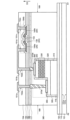
- FIG. 23 is a cross-sectional view showing an example of the cross-sectional structure of a pixel 180A of the display device 20. Specifically, it is a cross-sectional view showing an example of the cross-sectional structure of the pixel 180A cut along the line B1-B2 shown in Fig. 22.
- Fig. 24 is a cross-sectional view showing an example of the cross-sectional structure of a peripheral region 121 and a part of the display region 122 of the display device 20.
- the backplane 200A includes a second substrate 401, a protective layer 417, a base layer 436, conductive layers 238a, 238b, and 438c, first connection conductive layers 244a and 244b, a source electrode 444a, a drain electrode 444b, an oxide semiconductor layer 442, a gate insulating layer 440, an insulating layer 446, an insulating layer 454, and an insulating layer 456.
- the backplane 200A includes a scanning signal line 129a and a transistor 484a.
- the transistor 484a includes at least a source electrode 444a, a drain electrode 444b, an oxide semiconductor layer 442, a portion of the gate insulating layer 440, and a portion of the insulating layer 446.
- the second substrate 401 is a substrate (second support substrate) that supports the terminals 150, the scanning signal line driving circuits 104, the scanning signal lines 129 including the scanning signal line 129a, the data signal lines 131, the ground wiring 145, and the driving potential line 147.
- the second substrate 401 includes a first surface 401a and a second surface 401b that faces the first surface 401a.
- the protective layer 417, the underlayer 436, the conductive layers 238a, 238b, and 438c, the first connecting conductive layers 244a and 244b, the source electrode 444a, the drain electrode 444b, the oxide semiconductor layer 442, the gate insulating layer 440, the insulating layer 446, the insulating layer 454, and the insulating layer 456 are disposed on the first surface 401a.
- the protective layer 417 is disposed on the first surface 401a of the second substrate 401.
- the protective layer 417 can prevent the diffusion of impurities from the second substrate 401 or impurities from the outside (e.g., moisture or sodium (Na)).
- the base layer 436 is disposed on the protective layer 417. Like the protective layer 417, the base layer 436 can prevent the diffusion of impurities from the second substrate 401 or impurities from the outside (e.g., moisture or sodium (Na)).
- the conductive layers 238a, 238b, and 438c are disposed on the base layer 436.
- the conductive layer 238a functions as the scanning signal line 129a.
- the conductive layer 238b functions as the driving potential line 147a.
- the conductive layer 438c functions as the gate electrode of the transistor 484a.
- the gate insulating layer 440 is disposed on the conductive layers 238a, 238b, and 438c, and on a portion of the base layer 436. That is, the gate insulating layer 440 is disposed so as to cover the multiple scanning signal lines 129, the driving potential line 147a, and the gate electrode of the transistor 484a. The gate insulating layer 440 insulates the multiple scanning signal lines 129, the driving potential line 147a, and the gate electrode of the transistor 484a from each other.
- the oxide semiconductor layer 442 is disposed on the gate insulating layer 440.
- the oxide semiconductor layer 442 is used for the channels of the multiple transistors 484.
- the multiple transistors 484 include the transistor 484a.
- the source electrode 444a and the drain electrode 444b are disposed on the oxide semiconductor layer 442 and the gate insulating layer 440.
- the source electrode 444a and the drain electrode 444b are electrically connected to the oxide semiconductor layer 442.
- the source electrode 444a and the drain electrode 444b of the display device 20 are directly connected to the oxide semiconductor layer 442.
- the source electrode, the drain electrode, and the wiring formed in the same layer as the source electrode and the drain electrode included in the pixel 180A when the source electrode, the drain electrode, and the wiring are not distinguished, the source electrode, the drain electrode, and the wiring are described as the conductive layer 444, and when the source electrode, the drain electrode, and the wiring are distinguished, the source electrode, the drain electrode, and the wiring are given individual reference characters such as the source electrode 444a, the drain electrode 444b, etc.
- Insulating layer 454 is disposed on insulating layer 446. Insulating layer 456 is disposed on insulating layer 454. A portion of insulating layer 456 is opened. In addition, a portion of insulating layer 454 and a portion of insulating layer 456 are opened to expose conductive layer 238b.
- the first connection conductive layer 244a is disposed on a part of the exposed insulating layer 456.
- the first connection conductive layer 244b is disposed on the exposed conductive layer 238b and is electrically connected to the conductive layer 238b.
- the first connection conductive layers 244a and 244b are formed on different layers in the same process.
- the first connection conductive layer 244a extends in the second direction D2 as shown in FIG. 4 and branches out and extends in the first direction D1.
- the first connection conductive layer 244a is disposed so as to overlap with the gate insulating layer 440.
- the first connection conductive layer 244b extends in the first direction D1 and the second direction D2 as shown in FIG. 3.
- the first connection conductive layer 244b may be disposed so as to overlap with the gate insulating layer 440.
- the adhesive resin material 610 is disposed on a portion of the insulating layer 456.
- the adhesive resin material 610 is formed so as to surround at least a portion of the periphery of the light-emitting diode 300 and the transistor 184, as in the cross-sectional view shown in FIG. 24.
- the adhesive resin material 610 is disposed on a portion of the insulating layer 456 so as to overlap the display region 122 without overlapping the peripheral region 121, as in the cross-sectional view shown in FIG. 23.
- the adhesive resin material 610 may overlap the peripheral region 121.
- the peripheral region 121 of the display device 20 (the periphery of the adhesive resin material 610) may be sealed with a resin or the like.
- the first surface 101a of the pixel IC chip 181 faces the first surface 401a of the backplane 200A, and the array substrate 100 is bonded to the backplane 200A.
- the array substrate 100 and the backplane 200A are bonded together by an adhesive resin material 610.
- the array substrate 100 is electrically connected to the backplane 200A by the conductive connection members 620a and 620b.
- the conductive layer 152a of the array substrate 100 is electrically connected to the first connection conductive layer 244a of the backplane 200A via the conductive connection member 620a
- the conductive layer 152c of the array substrate 100 is electrically connected to the first connection conductive layer 244b of the backplane 200A via the conductive connection member 620b.
- the conductive layer 238b and the first connection conductive layer 244b may overlap the second transistor 184b.
- the conductive layer 238b (first connection conductive layer 244b) and the oxide semiconductor layer 142 can form a capacitor 188 via the insulating layers 119, 118, 154, and 146.
- the display device 20 having the above-described configuration has the same effect as the display device 10.
- the peripheral region 121 of the display device 20 includes the scanning signal line driving circuit 104
- the display device 20 can reduce the step caused by the thickness of the peripheral region 121 and the thickness of the display region 122 more than a display device that does not include the scanning signal line driving circuit 104.
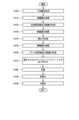
- FIG. 25 is a flow chart showing an example of a manufacturing method for the backplane 200A and an example of a method for bonding the pixel IC chip 181 and the backplane 200A.
- Figures 26 to 30 are cross-sectional views showing an example of a cross-sectional structure in the manufacturing process of the backplane 200A. Configurations that are the same as or similar to those in Figures 1 to 24 will be described as necessary.
- the manufacturing method for the array substrate 100 is the same as the manufacturing method for the array substrate 100 of the display device 10 described in "1-5", and the manufacturing method for the array substrate 100 will be described as necessary.
- the method for manufacturing the backplane 200A includes steps S700 to S810. As with the method for manufacturing the backplane 200, the method for manufacturing the backplane 200A uses a second substrate 401, such as an amorphous glass substrate, as a support substrate.
- a second substrate 401 such as an amorphous glass substrate
- Step S700 is a step of forming a protective layer 417 on the first surface 401a of the second substrate 401 so as to be in contact with the first surface 401a (see Figures 25 and 26).
- the protective layer 417 is formed on the first surface 401a using CVD, using a material similar to that of the insulating layer 117 in step S210.
- the protective layer 417 can prevent impurities from the second substrate 401 or external impurities (e.g., moisture or sodium (Na)) from diffusing into layers stacked on the underlayer 436.
- Step S710 is a step of forming an underlayer 436 on the protective layer 417 so as to be in contact with the protective layer 417 (see Figures 25, 26, and 27).
- the underlayer 436 can be formed in the same manner as the underlayer 110 in step S110 using the same material.
- the underlayer 436 can prevent impurities from the second substrate 401 or external impurities (e.g., moisture or sodium (Na)) from diffusing into layers stacked on the underlayer 436.
- Step S720 is a step of forming a conductive film on the underlayer 436 so as to be in contact with the underlayer 436 (see FIG. 25, FIG. 26, and FIG. 27).
- Step S730 is a step of processing the conductive film formed in step S720 using photolithography and etching to form gate electrodes of multiple transistors, multiple scanning signal lines 129a and 129, driving potential lines 147, 147a, 147b, and 147c, and each wiring.
- the conductive layers 238a and 238b shown in FIG. 26 include a conductive film, the conductive layer 238a functions as the scanning signal line 129a, and the conductive layer 238b functions as the driving potential line 147a.
- the conductive layer 438c and the scanning signal line 129a shown in FIG. 27 include a conductive film, and the conductive layer 438c functions as the gate electrode of the transistor 484a.
- the conductive layers 238a and 238b, the conductive layer 438c, and the scanning signal line 129a are formed by sputtering using the same material as the conductive layer 138 formed in step S250, and are formed by photolithography and etching in the same manner as in step S260.
- Step S750 is a step of depositing an oxide semiconductor layer 442 on the gate insulating layer 440 by sputtering so as to be in contact with the gate insulating layer 440 (see Figures 25, 26, and 27).
- the oxide semiconductor layer 442 is deposited on the gate insulating layer 440 using the same material as the oxide semiconductor layer 142.
- Step S760 is a step of processing the oxide semiconductor layer 442 formed in step S750 using photolithography and etching to form the oxide semiconductor layer 442 used in each semiconductor layer of the multiple transistors 484 (see Figures 25, 26, and 27). Note that, for example, after step S760, an opening 441a is formed using photolithography and etching. The opening 441a exposes a part of the surface of the gate insulating layer 440 and the scanning signal line 129a that form the sidewall of the opening 441a.
- Step S770 is a step of depositing a conductive layer 444 by sputtering on the oxide semiconductor layer 442, on a portion of the surface of the scanning signal line 129a, on the sidewall of the opening 441a, and on a portion of the gate insulating layer 440 so as to be in contact with the oxide semiconductor layer 442, the portion of the surface of the scanning signal line 129a, the sidewall of the opening 441a, and a portion of the gate insulating layer 440.
- the conductive layer 444 can be formed using the same material as the conductive layer 144.
- Step S780 is a step in which the conductive layer 444 formed in step S770 is processed using photolithography and etching to form a source electrode, a drain electrode, and a wiring (see FIG. 25 and FIG. 29).
- the conductive layer 444 functions as a source electrode, a drain electrode, or a wiring.
- the conductive layer 444 shown in FIG. 29 is a source electrode 444a and a drain electrode 444b.
- Step S790 is a step of forming an insulating layer 446 by CVD on the conductive layer 444, on a part of the oxide semiconductor layer 442, and on a part of the gate insulating layer 440 so as to be in contact with the conductive layer 444, a part of the oxide semiconductor layer 442, and a part of the gate insulating layer 440, forming an insulating layer 454 on the insulating layer 446 so as to be in contact with the insulating layer 446, and forming an insulating layer 456 on the insulating layer 454 so as to be in contact with the insulating layer 454 (see FIG. 25, FIG. 28, and FIG. 29).
- the insulating layer 446 can be formed using a material similar to that of the gate insulating layer 440.
- the insulating layer 454 can be formed using a material similar to that of the insulating layer 380.
- the insulating layer 454 can planarize unevenness due to the transistor 484 and the insulating layer 446, like the insulating layer 380.
- the insulating layer 456 can be formed using a material similar to that of the insulating layer 117. Similar to the insulating layer 117, the insulating layer 456 can prevent impurities from the outside (e.g., moisture or sodium (Na)) from diffusing into layers below the insulating layer 456.
- impurities from the outside e.g., moisture or sodium (Na)
- Step S800 is a step of forming openings 443a and 443b using photolithography and etching.
- Opening 443a exposes insulating layers 446, 454, and 456, which form the sidewalls of opening 443a, and a portion of the surface of conductive layer 238b.
- Opening 443b exposes insulating layers 456 and a portion of the surface of insulating layer 454, which form the sidewalls of opening 443b (see Figures 25 and 28).
- Step S810 is a step of forming a conductive layer. Specifically, this is a step of forming a conductive film so as to contact the insulating layers 446, 454, and 456 that form the side walls of the opening 443a, a part of the surface of the conductive layer 238b, the insulating layer 456 that forms the side walls of the opening 443b, and a part of the surface of the insulating layer 454 (see Figures 25 and 30).
- the conductive film is formed on the insulating layer and the conductive layer using sputtering and ECP, as in step S340.
- the formed conductive layer is polished using CMP and planarized until the surface of the insulating layer 456 is exposed.
- the first connection conductive layers 244a and 244b can be formed.
- the first connection conductive layers 244a and 244b shown in FIG. 30 include a conductive film
- the first connection conductive layer 244a functions as the ground wiring 145a
- the first connection conductive layer 244b is electrically connected to the conductive layer 238b and functions as the driving potential line 147a.
- the first connection conductive layers 244c and 244d are formed in the same manner as the first connection conductive layers 244a and 244b.
- the first connection conductive layer 244c (see FIG. 3) is electrically connected to the conductive layer 238a and functions as the scanning signal line 129.
- the first connection conductive layer 244d functions as the data signal line 131.
- the conductive film formed in step S810 can be made of the same material as the conductive film formed in step S340.
- the conductive film can be a conductive layer made of manganese and copper.
- the display device 20 can suppress the diffusion of copper into the insulating layer in contact with the first connection conductive layer 244, and can absorb hydrogen discharged from the insulating layer in contact with the first connection conductive layer, thereby suppressing the deterioration of the electrical characteristics of the transistor 484.
- the first connection conductive layer 244 is formed using ECP, it can be formed thicker than films and layers formed using sputtering or CVD.
- the resistance value of the data signal line 131 (first connection conductive layer 244d) and the ground wiring 145a (first connection conductive layer 244a) formed using the first connection conductive layer 244 can be made even smaller than the resistance value of wiring formed using a material with a higher resistivity than copper.
- the time constant of the signal supplied to the data signal line 131 is improved, and the amount of charge supplied to the ground wiring 145a is increased.
- the backplane 200A is formed.
- Steps S820 to S850 are the same as steps S450 to S500. Therefore, a description of steps S820 to S850 will be omitted here.
- the manufacturing method of the display device 20 can electrically connect the pixel IC chip 181 (first surface 101a of the array substrate 100) to the backplane 200A.
- the pixel IC chip 181 which includes the light-emitting diode 300 and the first to third transistors 184a to 184c, is electrically connected to the data signal line 131, the scanning signal line 129, the ground wiring 145, and the drive potential line 147 included in the backplane 200A.
- the manufacturing method for the display device 20 including the above configuration has the same effect as the manufacturing method for the display device 10. Furthermore, since the manufacturing method for the display device 20 includes forming the scanning signal line driving circuit 104 in the peripheral region 121, the number of parts mounted on the display device 20 can be reduced compared to the case where an IC chip including a scanning signal line driving circuit is mounted on the display device 20. As a result, the manufacturing method for the display device 20 is a manufacturing method that can reduce costs.
- the transistor 484 included in the backplane 200A can be covered on the second substrate 401 side and on the second substrate 401 side and the third direction D3 side with insulating layers 471 and 456 using AlO.
- impurities e.g., moisture or sodium (Na)
- the manufacturing method of the display device 20 can suppress deterioration of the electrical characteristics of the transistor 484.
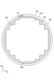
- FIG. 31 is a plan view showing an example of the protection circuit 460. Configurations that are the same as or similar to those in Figs. 1 to 30 will be described as necessary.
- the protection circuit 460 is electrically connected to the terminal 150 and the data signal line 131 connected to the terminal 150.
- the protection circuit 460 includes transistors 484b and 484c.
- the conductive states of the transistors 484b and 484c are controlled by signals supplied to signal lines or wiring electrically connected to the protection circuit 460.
- the transistor 484b includes a gate electrode 4G, a source electrode 4S, and a drain electrode 4D.
- the transistor 484c includes a gate electrode 5G, a source electrode 5S, and a drain electrode 5D.
- the source electrode 4S is electrically connected to the driving potential line 147
- the drain electrode 4D is electrically connected to the gate electrode 4G, the data signal line 131, and the source electrode 5S.
- the drain electrode 5D is electrically connected to the gate electrode 5G and the ground wiring 145.
- the drain electrode 4D is electrically connected to the gate electrode 4G and the data signal line 131. Therefore, when the potential supplied to the data signal line 131 is greater than the potential supplied to the drive potential line 147, the transistor 484b becomes conductive and functions as a protection circuit. In other words, when an overvoltage is supplied to the data signal line 131 via the terminal 150, a current can be passed from the drain electrode 4D to the drive potential line 147 via the transistor 484b. As a result, the transistor 484b can suppress the application of an overvoltage and the supply of an overcurrent to the data signal line 131.
- the drain electrode 5D is also electrically connected to the gate electrode 5G and the ground wiring 145. Therefore, when the potential supplied to the source electrode 5S is lower than the potential supplied to the ground wiring 145, the transistor 484c is in a conductive state and functions as a protection circuit. In other words, when an overvoltage is supplied to the data signal line 131 via the terminal 150, a current can be passed from the ground wiring 145 to the source electrode 5S via the transistor 484c. As a result, the transistor 484c can suppress the application of an overvoltage and the supply of an overcurrent to the data signal line 131.
- the transistors 484b and 484c like the transistor 484a and the multiple transistors 184, include an oxide semiconductor layer 442 and are formed on the second substrate 401.
- the leakage current and off current of the transistors 484b and 484c are smaller than the leakage current and off current of a transistor including amorphous silicon or polysilicon. Therefore, the leakage current and off current of the protection circuit 460 are small, so that the application of an overvoltage and the supply of an overcurrent to the data signal line 131 can be efficiently suppressed.
- the protection circuit 460 can suppress the deterioration of electrical characteristics caused by the leakage current and off current.
- the temperature characteristics of the off current of a transistor formed using an oxide semiconductor layer are superior to the temperature characteristics of the off current of a transistor formed using amorphous silicon or polysilicon. Therefore, the display device 20 includes a protection circuit using a transistor with excellent temperature characteristics, so that the deterioration of long-term reliability can be suppressed.
Landscapes
- Physics & Mathematics (AREA)
- General Physics & Mathematics (AREA)
- Engineering & Computer Science (AREA)
- Theoretical Computer Science (AREA)
- Optics & Photonics (AREA)
- Devices For Indicating Variable Information By Combining Individual Elements (AREA)
Abstract
表示装置は、第1の基板と、前記第1の基板の第1の面の上に配置され、窒化ガリウム層を含む発光ダイオードと、前記発光ダイオードの上に配置され、前記発光ダイオードと電気的に接続された第1のトランジスタと、前記第1の基板に対向する第2の基板と、前記第2の基板の上に配置されたデータ信号線と、前記第2の基板の上に配置されたグラウンド信号線と、前記データ信号線の上に配置され、前記データ信号線と前記第1のトランジスタとを電気的に接続する第1の導電体と、前記グラウンド信号線の上に配置され、前記グラウンド配線と前記発光ダイオードとを電気的に接続する第2の導電体とを含む。
Description
本発明の実施形態の一つは、酸化物半導体を用いたトランジスタ及び窒化ガリウムを用いた発光素子を含む表示装置に関する。
近年、窒化ガリウム(GaN)を用いた発光素子を表示部に用いた表示装置が知られている。例えば、発光素子は、発光ダイオード(Light Emitting Diode:LED)又は微小な発光ダイオード(マイクロLED)である。例えば、当該表示装置は、発光素子が形成されたサファイア基板と、酸化物半導体又は低温ポリシリコンを含むトランジスタが形成されたバックプレーンとを含み、当該表示装置の製造方法は、サファイア基板をバックプレーンに転写することによって発光素子とトランジスタとを電気的に接続することを含む。このように製造された当該表示装置の発光素子は、トランジスタに供給された電位に応じた電流を流すことができる。その結果、発光素子は発光し、当該表示装置は表示部に画像を表示することができる。
例えば、特許文献1~4は、トランジスタ及び発光素子を含む表示装置を開示している。
例えば、当該表示装置の製造方法は、発光素子を転写してバックプレーンのトランジスタに接続することを含む。発光素子とトランジスタとの電気的な接続が安定せず、発光素子とトランジスタとのボンディングに応じてコンタクト抵抗がばらつく可能性がある。また、発光素子とトランジスタとの電気的な接続が安定していない場合、又は、トランジスタの電気特性が安定していない場合には、トランジスタが発光素子に所定の電位に応じた電流を供給できない可能性がある。その結果、発光素子が所定の輝度で発光しないため、表示装置が所定の電位に応じた画像を表示することができない。また、発光素子とトランジスタとの電気的な接続が安定していない場合、又は、トランジスタの電気特性が安定していない場合には、トランジスタの長期信頼性及び表示装置の長期信頼性が問題になる。
本発明の課題の一つは、酸化物半導体を用いたトランジスタ及び窒化ガリウムを用いた発光素子を含み、長期信頼性の低下を抑制可能な表示装置を提供することを課題の一つとする。
本発明の実施形態の一つに係る表示装置は、第1の基板と、前記第1の基板の第1の面の上に配置され、窒化ガリウム層を含む発光ダイオードと、前記発光ダイオードの上に配置され、前記発光ダイオードと電気的に接続された第1のトランジスタと、前記第1の基板に対向する第2の基板と、前記第2の基板の上に配置されたデータ信号線と、前記第2の基板の上に配置されたグラウンド配線と、前記データ信号線の上に配置され、前記データ信号線と前記第1のトランジスタとを電気的に接続する第1の導電体と、前記グラウンド配線の上に配置され、前記グラウンド配線と前記発光ダイオードとを電気的に接続する第2の導電体とを含む。
以下、本発明の実施形態を、図面等を参照しながら説明する。但し、本発明は多くの異なる態様で実施することが可能であり、以下に例示する実施の形態の記載内容に限定して解釈されるものではない。また、図面は説明をより明確にするため、実際の態様に比べ、各部の幅、厚さ、形状、構成等について模式的に表される場合があるが、あくまで一例であって、本発明の解釈を限定するものではない。また、本発明の実施形態において、既出の図に関して前述したものと同様の要素には、同一の符号(又は数字の後にa、bなどを付した符号)を付して、詳細な説明を適宜省略することがある。なお、各要素に対する「第1」、「第2」と付記された文字は、各要素を区別するために用いられる便宜的な標識であり、特段の説明がない限りそれ以上の意味を有さない。
本願の明細書において、ある部材又は領域が他の部材又は領域の「上に(又は下に)」あるとする場合、特段の限定がない限りこれは他の部材又は領域の直上(又は直下)にある場合のみでなく他の部材又は領域の上方(又は下方)にある場合を含み、すなわち、他の部材又は領域の上方(又は下方)において間に別の構成要素が含まれている場合も含む。
本願の明細書において、D1方向はD2方向に交差し、D3方向はD1方向及びD2方向(D1D2平面)に交差する。D1方向は第1方向といわれ、D2方向は第2方向といわれ、D3方向は第3方向といわれる。例えば、D1方向、D2方向、及びD3方向は、X方向(x方向)、Y方向(y方向)、及びZ方向(z方向)に対応する。なお、D3方向が、D1方向及びD2方向に対して、垂直から誤差の範囲内でずれた場合も、D3方向は、D1方向及びD2方向に垂直であるものとする。この場合は、例えば、略垂直と呼ばれる。
本願の明細書において、同一及び一致という表記を用いている場合、同一及び一致には、設計の範囲での誤差が含まれてもよい。
[1.第1実施形態]
図1~図21を参照し、表示装置10の構成を説明する。
図1~図21を参照し、表示装置10の構成を説明する。
[1-1.表示装置10の概要]
図1を参照し、表示装置10の概要を説明する。図1は表示装置10の構成を示す模式的な平面図である。
図1を参照し、表示装置10の概要を説明する。図1は表示装置10の構成を示す模式的な平面図である。
表示装置10は、少なくとも、第1の基板101(図5を参照)、第2の基板201、フレキシブルプリント回路基板(FPC)108及びドライバIC106を含む。また、表示装置10は、少なくとも、第2の基板201(図5を参照)の第1の面201a(図5を参照)の上の表示領域122及び表示領域122の周囲を取り囲む周辺領域121を含む。なお、詳細は後述するが、アレイ基板100(図5を参照)が第1の基板101を含み、バックプレーン200(図5を参照)が第2の基板201を含む。
第2の基板201は、第1の辺191、第1の辺に対向する第2の辺192、第3の辺193、及び第3の辺に対向する第4の辺194を含む。表示領域122及び周辺領域121は、平面視において、第1の辺191、第1の辺に対向する第2の辺192、第3の辺193、及び第3の辺193に対向する第4の辺194に囲まれる。
表示領域122には、複数の画素180が配置されている。表示領域122は、複数の画素180と平面視において重なる領域である。複数の画素180は第1方向D1及び第2方向D2にマトリクス状に配置される。複数の画素180の配置は、マトリクス状に限定されない。例えば、複数の画素180は千鳥状に配置されてもよい。詳細は後述されるが、画素180は、画素ICチップ181を含む。
周辺領域121は、複数の走査信号線129、複数のデータ信号線131、グラウンド配線145、駆動電位線147及び端子領域126を含む。周辺領域121は、複数の走査信号線129、複数のデータ信号線131、グラウンド配線145、駆動電位線147及び端子領域126と平面視において重なる領域である。複数の走査信号線129、複数のデータ信号線131、グラウンド配線145及び駆動電位線147は、複数の画素180のうち、対応する画素180に電気的に接続される。
端子領域126は第3の辺193側の領域である。複数の端子150が端子領域126に配置されている。複数の端子150は、FPC108、複数の走査信号線129、複数のデータ信号線131、グラウンド配線145及び駆動電位線147に電気的に接続される。端子領域126は、複数の走査信号線129、複数のデータ信号線131、グラウンド配線145及び駆動電位線147を、FPC108、ドライバIC106及び外部回路(図示は省略)と接続するための複数の端子150と平面視において重なる領域である。なお、複数の端子150は、第2の基板201に含まれ、FPC108と重なる。
一例として、ドライバIC106は、FPC108上に配置される。ドライバIC106は、複数の画素180を駆動させるための制御信号を、FPC108、走査信号線129、データ信号線131、グラウンド配線145及び駆動電位線147を介して、複数の画素180に供給する。
グラウンド配線145は、表示領域122を囲むように配置される。また、グラウンド配線145は、第1の辺191側の端子150に電気的に接続され第3の辺193に沿ってD1方向に延在する配線と、第1の辺191に沿ってD2方向に延在する配線と、第4の辺194に沿ってD1方向に延在する配線と、第2の辺192に沿ってD2方向に延在する配線と、第2の辺192側の端子150に電気的に接続され第3の辺193に沿ってD1方向に延在する配線と、を含む。さらに、グラウンド配線145は、第4の辺194に沿ってD1方向に延在する配線と電気的に接続され、D2方向に沿って第4の辺194側から第3の辺193側に向かって分岐されたグラウンド配線145a、145b及び145cを含む。例えば、グラウンド配線145には、グラウンド電圧、接地電圧、電圧VSS、0Vなどの定電位が供給される。これらの電圧(電位)は各信号の基準となる電位であり、基準電圧(電位)と呼ばれてよい。
駆動電位線147は、第1の辺191側の端子150に電気的に接続され第3の辺193に沿ってD1方向に延在する配線と、第1の辺191に沿ってD2方向に延在する配線と、を含む。また、駆動電位線147は、第1の辺191に沿ってD2方向に延在する配線と電気的に接続され、D1方向に沿って第1の辺191側から第2の辺192側に向かって分岐された駆動電位線147a、147b及び147cを含む。駆動電位線147a、147b及び147cは、それぞれ、D1方向に沿って配置される複数の画素ICチップ181に電気的に接続される。例えば、駆動電位線147には、グラウンド配線145に供給される電位より高い定電位が供給される。グラウンド配線145に供給される電位より高い定電位は、例えば、電圧VDD、30Vなどの電位である。駆動電位線147は、グラウンド配線145と同様に、表示領域122を囲むように配置されてよい。
以上説明した構成を含むグラウンド配線145は、グラウンド電圧などの定電位を複数の画素ICチップ181に均一に供給することができる。また、以上説明した構成を含む駆動電位線147は、電圧VDDなどの定電位を複数の画素ICチップ181に均一に供給することができる。その結果、表示装置10は、ムラの無い画像を表示領域122に表示することができる。
[1-2.画素180の構成]
図2及び図3を参照し、画素180の構成を説明する。図2は表示装置10の画素180の画素回路182の構成を示す模式的な回路図である。図3は画素回路182を含む画素ICチップ181と、走査信号線129、データ信号線131、グラウンド配線145及び駆動電位線147との電気的な接続を示す模式的な図である。図1と同一、又は類似する構成については、必要に応じて説明する。
図2及び図3を参照し、画素180の構成を説明する。図2は表示装置10の画素180の画素回路182の構成を示す模式的な回路図である。図3は画素回路182を含む画素ICチップ181と、走査信号線129、データ信号線131、グラウンド配線145及び駆動電位線147との電気的な接続を示す模式的な図である。図1と同一、又は類似する構成については、必要に応じて説明する。
画素180は、走査信号線129、データ信号線131、グラウンド配線145及び駆動電位線147に電気的に接続された画素ICチップ181を含む。
画素ICチップ181は、第1のトランジスタ184a、第2のトランジスタ184b、第3のトランジスタ184c、発光ダイオード300及び容量素子188を含む。また、画素ICチップ181は、第1の接続導電層244a、244b、244c及び244dを含む。例えば、第1の接続導電層244a、244b、244c及び244dは、半田又は異方性導電膜(ACF)を用いて、それぞれに対応する電極と配線とを接続する。例えば、第1の接続導電層244aはゲート電極3G、ソース電極3S及び陰極6Fとグラウンド配線145aとの間に配置されると共に接続し、第1の接続導電層244bはドレイン電極2D及び第2の電極8Sと、駆動電位線147aとの間に配置されると共に接続し、第1の接続導電層244cはゲート電極1Gと走査信号線129との間に配置されると共に接続し、第1の接続導電層244dはソース電極1Sとデータ信号線131との間に配置されると共に接続する。
画素180に含まれる第1の接続導電層の説明において、第1の接続導電層を区別しない場合には、第1の接続導電層は第1の接続導電層244と記載され、第1の接続導電層を区別する場合には、第1の接続導電層は第1の接続導電層244a~244dなどと個別の符号が付与される。
第1のトランジスタ184aは、選択トランジスタとして機能することができる。第1のトランジスタ184aの導通状態は、走査信号線129により制御される。第1のトランジスタ184aは、ゲート電極1G、ソース電極1S及びドレイン電極1Dを含む。ソース電極1Sは、データ信号線131に電気的に接続され、ドレイン電極1Dは、第2のトランジスタ184bのゲート電極2G及び容量素子188の第1の電極8Fと電気的に接続され、ゲート電極1Gは走査信号線129に電気的に接続される。
第2のトランジスタ184bは、駆動トランジスタとして機能することができる。第2のトランジスタ184bは、発光ダイオード300の発光輝度を制御する。第2のトランジスタ184bの導通状態は、第1のトランジスタ184aにより制御される。第2のトランジスタ184bは、ゲート電極2G、ソース電極2S及びドレイン電極2Dを含む。ソース電極2Sは、第3のトランジスタ184cのドレイン電極3D及び発光ダイオード300の陽極6Sと電気的に接続され、ドレイン電極2Dは駆動電位線147及び容量素子188の第2の電極8Sと電気的に接続され、ゲート電極2Gは、ドレイン電極1D及び第1の電極8Fと電気的に接続される。
第3のトランジスタ184cは、発光ダイオード300の保護回路として機能することができる。第3のトランジスタ184cは、ゲート電極3G、ソース電極3S及びドレイン電極3Dを含む。第3のトランジスタ184cは発光ダイオード300に並列に接続される。より具体的には、ソース電極3Sは、ゲート電極3G、発光ダイオード300の陰極6F及びグラウンド配線145と電気的に接続され、ドレイン電極3Dは、陽極6S及びソース電極2Sと電気的に接続される。ゲート電極3Gはソース電極3Sと電気的に接続され、第3のトランジスタ184cは、所謂、ダイオード接続を含むダイオードである。第3のトランジスタ184cの導通状態は、ドレイン電極3Dに供給される電位とソース電極3Sに供給される電位との電位差により制御される。ソース電極3Sがグラウンド配線145と電気的に接続されているため、ドレイン電極3Dに供給される電位は、基本的には、グラウンド配線145に供給される電位以上である。ドレイン電極3Dに供給される電位がグラウンド配線145に供給される電位より小さい場合に、第3のトランジスタ184cは導通状態となり、保護回路として機能する。すなわち、過電圧が、発光ダイオード300の陽極6Sと陰極6Fとの間に印加された場合には、画素180(画素回路182)は発光ダイオード300に流れる電流を第3のトランジスタ184cを経由して、グラウンド配線145に流すことができる。その結果、第3のトランジスタ184cは発光ダイオード300への過電圧の印加及び過電流の供給を抑制できる。
画素180に含まれるトランジスタの説明において、トランジスタを区別しない場合には、トランジスタはトランジスタ184と記載され、トランジスタを区別する場合には、トランジスタは第1のトランジスタ184a、第2のトランジスタ184b、第3のトランジスタ184cと記載される。
発光ダイオード300は陰極(n型電極)6F及び陽極(p型電極)6Sを含む。
容量素子188は第1の電極8F及び第2の電極8Sを含む。例えば、容量素子188は、画素180が表示する画像に対応する電位に相当する電荷を保持することができる。また、例えば、容量素子188は、第2のトランジスタ184bの閾値電圧に相当する電荷を保持し、第2のトランジスタ184bの閾値電圧を補正することができる。その結果、第2のトランジスタ184bは、画像に対応する電位に相当する安定した電流を、発光ダイオード300に供給することができる。
任意の制御信号が、ドライバIC106及び外部回路から、表示装置10の複数の画素180の画素回路182に供給され、表示装置10は表示領域122に画像を表示することができる。
なお、本明細書及び図面において、説明の便宜上、各トランジスタのソース電極及びドレイン電極に供給される電位によって、各々の電極のソースとしての機能とドレインとしての機能とが入れ替わる場合がある。
[1-3.レイアウトの例]
図4を参照し、第3のトランジスタ184c及び発光ダイオード300のレイアウトの一例を説明する。図4は第3のトランジスタ184c及び発光ダイオード300のレイアウトの一例を示す模式的な平面図である。図1~図3と同一、又は類似する構成については、必要に応じて説明する。
図4を参照し、第3のトランジスタ184c及び発光ダイオード300のレイアウトの一例を説明する。図4は第3のトランジスタ184c及び発光ダイオード300のレイアウトの一例を示す模式的な平面図である。図1~図3と同一、又は類似する構成については、必要に応じて説明する。
発光ダイオード300のn型電極350(陰極6F)は、第2の接続導電層370a、導電層152a及び導電性接続部材620aに接続され、第2の接続導電層370a、導電層152a及び導電性接続部材620aを介して、第1の接続導電層244a及びグラウンド配線145aに接続される。n型電極350(陰極6F)は、第2の接続導電層370a及び導電層152aを介して、開口139から露出したゲート電極138a(ゲート電極3G)及び開口140aから露出したソース電極3Sに接続される。発光ダイオード300のp型電極360(陽極6S)は、第2の接続導電層370b及び導電層152bに接続され、第2の接続導電層370b及び導電層152bを介して、開口140bから露出したドレイン電極3Dに接続される。
すなわち、第3のトランジスタ184c及び発光ダイオード300は同一ICチップ(画素ICチップ181)に備えられる。また、「1-2」で説明した通り、第3のトランジスタ184cは発光ダイオード300の保護回路として機能する。表示装置10は、発光ダイオード300と発光ダイオード300を保護する第3のトランジスタ184cとを個別に備えるのではなく、発光ダイオード300と発光ダイオード300を保護する第3のトランジスタ184cとを一体形成した構成を備えることができる。その結果、発光ダイオード300と発光ダイオード300を保護する第3のトランジスタ184cとを個別に備えるより、発光ダイオード300と第3のトランジスタ184cとの電気的な接続を安定させることができる。よって、表示装置10は、発光ダイオード300と第3のトランジスタ184cとコンタクト抵抗のばらつきを抑制すると共に、発光ダイオード300及び第3のトランジスタ184cの電気特性を安定させることができるため、画素180の発光特性、温度特性などの低下を抑制することができる。
[1-4.画素180の断面の一例]
図5を参照し、画素180の断面の一例を説明する。図5は、表示装置10の画素180の断面構造の一例を示す断面図である。具体的には、図1に示すA1-A2線で切断された画素180の断面構造の一例を示す断面図である。図1~図4と同一、又は類似する構成については、必要に応じて説明する。
図5を参照し、画素180の断面の一例を説明する。図5は、表示装置10の画素180の断面構造の一例を示す断面図である。具体的には、図1に示すA1-A2線で切断された画素180の断面構造の一例を示す断面図である。図1~図4と同一、又は類似する構成については、必要に応じて説明する。
表示装置10は、アレイ基板100及びバックプレーン200を含む。アレイ基板100は、第1の基板101、下地層110、バッファー層120、発光ダイオード300、絶縁層380、絶縁層117、絶縁層136、第2のトランジスタ184b、絶縁層154、導電層152a、152b及び152c、絶縁層118、絶縁層119、開口619a及び619b、色変換層115を含む。バックプレーン200は、第2の基板201、下地層210、複数の端子150(図1を参照)、導電層238a及び238b、第1の接続導電層244a及び244b、絶縁層240及び絶縁層246を含む。
第1の基板101はトランジスタ184及び発光ダイオード300を支持する基板(第1の支持基板)である。第1の基板101は第1の面101a及び第1の面101aに対向する第2の面101bを含む。バッファー層120、発光ダイオード300、絶縁層380、絶縁層117、絶縁層136、第2のトランジスタ184b、絶縁層154、導電層152a、152b及び152c、絶縁層118、絶縁層119、開口619a及び619bは、第1の面101a上に配置される。また、色変換層115は第2の面101b上に配置される。
下地層110は第1の基板101上に配置される。バッファー層120は下地層110上に配置される。
発光ダイオード300はバッファー層120上に配置される。発光ダイオード300は、窒化ガリウム層310、n型半導体層320、発光層330、p型半導体層340、n型電極350及びp型電極360を含む。
窒化ガリウム層310はバッファー層120上に配置される。n型半導体層320は窒化ガリウム層310上に配置される。発光層330は、n型半導体層320上に配置される。p型半導体層340は、発光層330上に配置される。n型電極350はn型半導体層320上に配置される。p型電極360はp型半導体層340上に配置される。
絶縁層116が発光ダイオード300を覆うように配置される。具体的には、絶縁層116は、バッファー層120の表面の一部、窒化ガリウム層310の側面、n型半導体層320の側面及び表面の一部、発光層330の側面、p型半導体層340の側面及び表面の一部に配置される。
また、発光ダイオード300は、所謂、マイクロLED又はミニLEDである。しかしながら、発光ダイオード300は、表示装置10に示されるLEDに限定されない。なお、マイクロLEDの一辺の長さは100μm以下であり、ミニLEDの一辺の長さは100μmより長い。
絶縁層380は、バッファー層120の表面の一部、発光ダイオード300及び絶縁層116を覆うように配置される。絶縁層117は絶縁層380上に配置される。絶縁層380は第1の平坦化膜と呼ばれる場合がある。
第2の接続導電層370aは開口372a(図10を参照)及びn型電極350と接し、開口372aを介してn型電極350と電気的に接続される。第2の接続導電層370bは開口372b(図10を参照)及びp型電極360と接し、開口372bを介してp型電極360と電気的に接続される。なお、開口372a及び372bが絶縁層117及び380に形成されるため、第2の接続導電層370aは開口372aの側壁となる絶縁層117及び380と接し、第2の接続導電層370bは372bの側壁となる絶縁層117及び380と接する。
絶縁層136は絶縁層117上に配置される。また、絶縁層136は、第2の接続導電層370a及び370bの表面上に配置される。例えば、絶縁層136は下地層である。
トランジスタ184は絶縁層136上に配置される。トランジスタ184は、導電層138、ゲート絶縁層140、酸化物半導体層142、ソース電極144a及びドレイン電極144bを含む。図5に示されるトランジスタ184は、一例として、第2のトランジスタ184bである。
導電層138は絶縁層136上に配置される。導電層138はゲート電極として機能する。例えば、図5に示される導電層138はゲート電極2Gである。
ゲート絶縁層140は、導電層138上及び絶縁層136の表面上に配置される。
酸化物半導体層142はゲート絶縁層140上に配置される。酸化物半導体層142はトランジスタ184のチャネルに用いられる。
ソース電極144a及びドレイン電極144bは、酸化物半導体層142上及びゲート絶縁層140上に、互いに離間して、配置される。ソース電極144a及びドレイン電極144bは、酸化物半導体層142と電気的に接続される。表示装置10のソース電極144a及びドレイン電極144bは酸化物半導体層142と直接接して接続される。なお、画素180に含まれるソース電極、ドレイン電極及びソース電極及びドレイン電極と同一層に形成される配線の説明において、ソース電極、ドレイン電極及び当該配線を区別しない場合には、ソース電極、ドレイン電極及び当該配線は導電層144と記載され、ソース電極、ドレイン電極及び当該配線を区別する場合には、ソース電極、ドレイン電極及び当該配線はソース電極144a、ドレイン電極144bなどと個別の符号が付与される。
絶縁層146は、ソース電極144a及びドレイン電極144b上、酸化物半導体層142の表面の一部の上、及びゲート絶縁層140の一部の上に配置される。すなわち、絶縁層146は、トランジスタ184を覆うように配置される。絶縁層154は、絶縁層146上に配置される。すなわち、絶縁層154はトランジスタ184を覆うように配置される。
導電層152aは、開口151a(図13を参照)及び第2の接続導電層370aと接し、開口151aを介して第2の接続導電層370aと電気的に接続される。導電層152bは、開口151b(図13を参照)及び第2の接続導電層370bと接し、開口151bを介して第2の接続導電層370bと電気的に接続される。また、導電層152bは、開口151d(図13を参照)及びソース電極144aと接し、開口151dを介してソース電極144aと電気的に接続される。導電層152cは、開口151c(図13を参照)及びドレイン電極144bと接し、開口151cを介してドレイン電極144bと電気的に接続される。なお、開口151a及び151bが、絶縁層136、ゲート絶縁層140、絶縁層146及び154に形成されるため、導電層152a及び152bは開口151a及び151bの側壁となる絶縁層136、ゲート絶縁層140、絶縁層146及び154と接する。開口151c及び151dが絶縁層146及び154に形成されるため、導電層152b及び152cは、開口151c及び151dの側壁となる絶縁層146及び154と接する。
絶縁層118は、絶縁層154、導電層152a、152b及び152c上に配置される。すなわち、絶縁層118は、導電層152a、152b及び152cを覆うように配置される。絶縁層119は絶縁層118上に配置される。
開口619a及び619bが絶縁層118及び119に形成される。導電性接続部材620aが開口619a及び導電層152aに接するように配置され、導電性接続部材620aは導電層152aに電気的に接続される。導電性接続部材620bが開口619b及び導電層152cに接するように配置され、導電性接続部材620bは導電層152cに電気的に接続される。導電性接続部材620a及び620bは導電体(第1の導電体及び第2の導電体)と呼ばれる場合がある。
接着樹脂材610がバッファー層120上に配置される。接着樹脂材610は、断面視において、発光ダイオード300及びトランジスタ184の周囲の少なくとも一部を取り囲むように形成される。
第2の基板201は、複数の端子150、複数の走査信号線129、複数のデータ信号線131、グラウンド配線145及び駆動電位線147を支持する基板(第2の支持基板)である。第2の基板201は第1の面201a及び第1の面201aに対向する第2の面201bを含む。下地層210、導電層238a及び238b、第1の接続導電層244a及び244b、絶縁層240及び絶縁層246は、第1の面201a上に配置される。
下地層210は第2の基板201上に配置される。下地層210は、第2の基板201からの不純物又は外部からの不純物(例えば、水分又はナトリウム(Na)など)の拡散を防止することができる。
導電層238a及び238bは下地層210上に配置される。導電層238aは走査信号線129として機能する。導電層238bは駆動電位線147aとして機能する。
絶縁層240は、導電層238a及び238b上に配置される。すなわち、絶縁層240は、複数の走査信号線129及び駆動電位線147aを覆うように配置される。また、絶縁層240には開口243が形成される。
第1の接続導電層244aが絶縁層240上に配置される。また、第1の接続導電層244bが絶縁層240の開口243において導電層238bの上に配置され、導電層238bと電気的に接続される。第1の接続導電層244a及び244bは異なる層上に同一の工程で形成される。例えば、第1の接続導電層244aは、図4に示されるように、第2方向D2に延在すると共に、第1方向D1に分岐し延在する。図示は省略されるが、第1の接続導電層244aは、絶縁層240と重畳するように配置される。例えば、第1の接続導電層244bは、図3に示されるように、第1方向D1及び第2方向D2に延在する。第1の接続導電層244bは、絶縁層240と重畳するように配置されてよい。
絶縁層246は、絶縁層240、第1の接続導電層244a及び244bの上に配置される。詳細は後述されるが、絶縁層246は、化学的機械研磨(Chemical Mechanical Polishing、CMP)を用いて研磨され、平坦化される。その結果、絶縁層246が第1の接続導電層244a及び244bの上から取り除かれ、絶縁層240の一部、第1の接続導電層244a及び244bがバックプレーンの表面に露出する。
例えば、複数の端子150は、導電層238及び第1の接続導電層244を用いて形成される。また、第1の接続導電層244の上の絶縁層240は開口され、第1の接続導電層244の上の絶縁層246はCMPを用いて研磨され、表面の露出された第1の接続導電層244がFPC300と電気的に接続される。
アレイ基板100の第1の面101aはバックプレーン200の第1の面201aと対向し、アレイ基板100はバックプレーン200に貼り合わされる。具体的には、アレイ基板100とバックプレーン200とは、接着樹脂材610によって、貼り合わされる。その結果、アレイ基板100は、導電性接続部材620a及び620bによって、バックプレーン200と電気的に接続される。具体的には、アレイ基板100の導電層152aが、導電性接続部材620aを介して、バックプレーン200の第1の接続導電層244aと電気的に接続され、アレイ基板100の導電層152cが、導電性接続部材620bを介して、バックプレーン200の第1の接続導電層244b電気的に接続される。例えば、このとき、導電層238b及び第1の接続導電層244bが第2のトランジスタ184bと重畳してよい。導電層238b(第1の接続導電層244b)と酸化物半導体層142とが、絶縁層119、118、154及び146を介して、容量素子188を形成することができる。
表示装置10の発光ダイオード300及び発光ダイオード300を駆動するための複数のトランジスタ184は、同一の第1の基板101上に形成することができる。発光ダイオード300と発光ダイオード300を駆動するための第2のトランジスタ184bとは、同一の第1の基板101上で電気的に接続される。その結果、表示装置10は、発光ダイオード及び発光ダイオードを駆動するためのトランジスタを含む画素ICチップ181をバックプレーンに転写することにより形成される。すなわち、画素ICチップ内の接触面積の小さな駆動トランジスタとLED接続部分では安定なアレイプロセスを利用し、接触面積の大きなバックプレーンと画素ICチップとの接続部分では転写プロセスを利用することによって、発光ダイオードとトランジスタとのコンタクト抵抗値を安定させることできる。よって、第2のトランジスタ184bによって発光ダイオード300に供給される電流が安定するため、表示装置10は、画素180の発光特性及び温度特性の低下を抑制することができる。
[1-5.表示装置10の製造方法の一例]
図6~図21を参照し、表示装置10の製造方法の一例を説明する。図6は、アレイ基板100の発光ダイオード300の製造方法の一例を示すフローチャートである。図7~図10は、アレイ基板100の製造過程における断面構造の一例を示す断面図である。図11は、アレイ基板100のトランジスタ184の製造方法の一例を示すフローチャートである。図12~図15は、アレイ基板100の製造過程における断面構造の一例を示す断面図である。図16は、アレイ基板100の製造方法の一例を示す平面図である。図17は、図16に示される平面を拡大した図である。図18は、バックプレーン200の製造方法の一例、及び、画素ICチップ181とバックプレーン200との張り合わせ方法の一例を示すフローチャートである。図19~20は、バックプレーン200の製造過程における断面構造の一例を示す断面図である。図21は、表示装置10の製造過程における断面構造の一例を示す断面図である。図1~図5と同一、又は類似する構成については、必要に応じて説明する。
図6~図21を参照し、表示装置10の製造方法の一例を説明する。図6は、アレイ基板100の発光ダイオード300の製造方法の一例を示すフローチャートである。図7~図10は、アレイ基板100の製造過程における断面構造の一例を示す断面図である。図11は、アレイ基板100のトランジスタ184の製造方法の一例を示すフローチャートである。図12~図15は、アレイ基板100の製造過程における断面構造の一例を示す断面図である。図16は、アレイ基板100の製造方法の一例を示す平面図である。図17は、図16に示される平面を拡大した図である。図18は、バックプレーン200の製造方法の一例、及び、画素ICチップ181とバックプレーン200との張り合わせ方法の一例を示すフローチャートである。図19~20は、バックプレーン200の製造過程における断面構造の一例を示す断面図である。図21は、表示装置10の製造過程における断面構造の一例を示す断面図である。図1~図5と同一、又は類似する構成については、必要に応じて説明する。
はじめに、図6~図17を参照し、アレイ基板100及び画素ICチップ181の製造方法を説明する。アレイ基板100及び画素ICチップ181の製造方法は、ステップS110~S380を含む。アレイ基板100及び画素ICチップ181の製造方法は、サファイア基板又は非晶質ガラス基板などの第1の基板101を支持基板として用いる。
ステップS110は、第1の基板101の第1の面101a上に、第1の面101aに接するように下地層110を形成するステップである(図6及び図7を参照)。例えば、下地層110はスパッタリングを用いて形成される。下地層110は、単層であってよく、積層であってもよい。例えば、下地層110は、窒化シリコン(SiNx)膜を単層として用いてよく、酸化シリコン(SiOx)膜と窒化シリコン(SiNx)膜との積層を用いてもよい。下地層110は、第1の基板101からの不純物又は外部からの不純物(例えば、水分又はナトリウム(Na)など)が下地層110に積層された層へ拡散することを防止することができる。
ステップS120は、下地層110上に下地層110に接するようにバッファー層120を形成するステップである(図6及び図7を参照)。例えば、バッファー層120はスパッタリングを用いて形成される。バッファー層120は、単層であってよく、積層であってもよい。また、バッファー層120は、第1の基板101に対してc軸配向していてよい。バッファー層120を設けることにより、発光ダイオード300の窒化ガリウム層310の結晶性を向上させることができる。発光ダイオード300の発光層330から発せられた光は、バッファー層120を透過して外部へ出射される。そのため、バッファー層120は、透光性を有する。例えば、バッファー層120は、窒化アルミニウム(AlN)膜などの透光膜を用いることができる。
ステップS130~S200は、発光ダイオード300を形成するステップである(図6及び図7を参照)。
ステップS130は、バッファー層120上に、バッファー層120に接するように窒化ガリウム(GaN)膜を成膜するステップである。ステップS140は、窒化ガリウム膜上に、窒化ガリウム膜に接するようにシリコン(Si)をドープした窒化ガリウム膜を成膜するステップである。ステップS150は、シリコンをドープした窒化ガリウム膜上に、シリコンをドープした窒化ガリウム膜に接するように、窒化インジウムガリウム(InGaN)膜と窒化ガリウム膜とが交互に積層された積層膜を成膜するステップである。ステップS160は、窒化インジウムガリウム膜と窒化ガリウム膜とが交互に積層された積層膜上に、マグネシウム(Mg)をドープした窒化ガリウム膜を成膜するステップである。ステップS130~S160は、スパッタリングを用いて、各膜を成膜するステップである。
ステップS170は、フォトリソグラフィー及びエッチングを用いて、窒化ガリウム層310、n型半導体層320、発光層330及びp型半導体層340を形成するステップである。窒化ガリウム層310は、ステップS130で成膜された窒化ガリウム膜を含む。窒化ガリウム層310はバッファー層120に接しているため、窒化ガリウム層310の結晶成長はバッファー層120によって制御される。具体的には、窒化ガリウム層310は第1の基板101に対してc軸配向した窒化ガリウム(GaN)膜を含む。n型半導体層320は、ステップS140で成膜されたシリコンをドープした窒化ガリウム膜を含む。n型半導体層320の表面の一部は、エッチングされ、露出される。発光層330は、ステップS150で成膜された、窒化インジウムガリウム膜と窒化ガリウム膜とが交互に積層された積層膜を含む。p型半導体層340は、ステップS160で成膜されたマグネシウムをドープした窒化ガリウム膜を含む。
ステップS180は、バッファー層120の表面の一部、窒化ガリウム層310の側面、n型半導体層320の側面及び表面の一部、発光層330の側面、p型半導体層340の側面及び表面の一部を覆うと共に接するように、絶縁層116を形成するステップである(図6及び図8を参照)。例えば、絶縁層116は、スパッタリングを用いて、酸化アルミニウム(AlO)膜を成膜し、フォトリソグラフィー及びエッチングを用いて形成される。酸化アルミニウム(AlO)膜は水素や水などへの耐性が高いため、絶縁層116は、発光ダイオード300を保護する保護膜として機能する。具体的には、絶縁層116は、水素や水などが発光ダイオード300に侵入すること、及び、水素や水などが発光ダイオード300内部に拡散することを防止することができる。また、例えば、絶縁層116の屈折率が、酸化シリコン(SiOx)膜の屈折率より大きい窒化シリコン(SiN)の場合には、絶縁層116は、発光ダイオード300からの出射光を反射することができる。その結果、絶縁層116は、発光ダイオード300からの出射光に基づくトランジスタ184の電気特性の変動を抑制できる。
ステップS190は、p型半導体層340上にp型電極360を形成するステップである。ステップS190の具体的な一例が以下で説明される。フォトリソグラフィー及びエッチングを用いて、絶縁層116の一部が開口され、p型半導体層340の一部が露出される。また、スパッタリングを用いてパラジウム(Pd)又は金(Au)などの金属膜あるいはニッケル(Ni)と金(Au)とを積層した金属などの積層金属膜が、p型半導体層340の一部の上及び絶縁層116の上に成膜され、フォトリソグラフィー及びエッチングを用いて、p型電極360がp型半導体層340上に形成される。p型電極360はパラジウム又は金などの金属膜あるいはニッケル(Ni)と金(Au)とを積層した金属などの積層金属膜を含む。p型電極360がp型半導体層340に電気的に接続される。
ステップS200は、n型半導体層320上にn型電極350を形成するステップである。ステップS200の具体的な一例が以下で説明される。フォトリソグラフィー及びエッチングを用いて、絶縁層116の一部が開口され、n型半導体層320の一部が露出される。また、スパッタリングを用いてインジウム(In)などの金属膜あるいはチタン(Ti)とアルミニウムチタン(AlTi)と金(Au)とを積層した金属などの積層金属膜が、n型半導体層320の一部の上及び絶縁層116の上に成膜され、フォトリソグラフィー及びエッチングを用いて、n型電極350がn型半導体層320の上に形成される。n型電極350はインジウムなどの金属膜あるいはチタンとアルミニウムチタンと金とを積層した金属などの積層金属膜を含む。n型電極350がn型半導体層320に電気的に接続される。
n型電極350とp型電極360とは、絶縁層116によって、互いに絶縁される。すなわち、n型電極350とp型電極360とは、絶縁層116によって、ショートされない。
なお、ステップS200とステップS190の順番が入れ替わってもよい。また、ステップS190とステップS200と同様の製造方法によって、p型電極360及びn型電極350が形成された後に、ステップS180と同様の製造方法によって絶縁層116が形成されてもよい。
以上説明したとおり、発光ダイオード300が形成される。
ステップS210は、バッファー層120の表面の一部、発光ダイオード300及び絶縁層116を覆うように、絶縁層380を形成するステップである(図6及び図9参照)。また、ステップS210は、絶縁層380上に絶縁層117を形成するステップである(図6及び図9参照)。具体的には、絶縁層380が、基板表面に膜を塗布する装置(塗布装置)を用いてバッファー層120の表面の一部、発光ダイオード300及び絶縁層116を覆うように成膜され、絶縁層117がスパッタリングを用いて絶縁層380の上に成膜される。絶縁層380及び絶縁層117が、フォトリソグラフィー及びエッチングを用いて形成される。その結果、複数の発光ダイオード300のそれぞれの周囲には、溝189が形成される。詳細は後述されるが、複数の発光ダイオード300のそれぞれは、溝189によって、個片化可能となっている。例えば、塗布装置としてスピンコーターあるいはスリットコーターを用いることができる。
例えば、絶縁層380は、アクリル樹脂膜又はポリイミド樹脂膜などの有機絶縁膜を用いることができる。絶縁層380は、有機絶縁膜を含むため、発光ダイオード300及び絶縁層116に基づく凹凸を平坦化することができる。絶縁層380は、単層であってよく、積層であってもよい。絶縁層380が積層膜である場合には、有機絶縁膜だけでなく、酸化シリコン(SiOx)膜又は窒化シリコン(SiNx)膜などの無機絶縁膜を含んでもよい
絶縁層117は絶縁層116と同様の材料を用いて形成される。例えば、絶縁層117は酸化アルミニウム(AlO)膜を用いて形成される。絶縁層117は、絶縁層116と同様に、水素や水などが絶縁層380及びトランジスタ184に侵入すること、及び、水素や水などが絶縁層380及びトランジスタ184内部に拡散することを防止することができる。また、絶縁層117の屈折率が、酸化シリコン(SiOx)の屈折率より大きい場合には、絶縁層117は、絶縁層116と同様に、発光ダイオード300からの出射光を反射することができる。その結果、絶縁層117は、絶縁層116と同様に、発光ダイオード300からの出射光に基づくトランジスタ184の電気特性の変動を抑制できる。
ステップS220は、フォトリソグラフィー及びエッチングを用いて、開口372b及び開口372aを形成するステップである(図6及び図10参照)。開口372aは、開口372aの側壁となる絶縁層117及び380、並びに、n型電極350の表面の一部を露出させる。開口372bは、開口372bの側壁となる絶縁層117及び380、並びに、p型電極360の表面の一部を露出させる。
ステップS230は、第2の接続導電層370a及び370bを成膜及び形成するステップである(図6及び図10参照)。ステップS230は、スパッタリングを用いて、開口372aの側壁となる絶縁層117及び380、n型電極350の表面の一部、開口372bの側壁となる絶縁層117及び380、並びに、p型電極360の表面の一部に、導電膜を成膜する。また、ステップS230は、フォトリソグラフィー及びエッチングを用いて、開口372aの側壁となる絶縁層117及び380、並びに、n型電極350の表面の一部に、第2の接続導電層370aを形成し、開口372bの側壁となる絶縁層117及び380、並びに、p型電極360の表面の一部に、第2の接続導電層370bを形成する。導電膜は、第2の接続導電層370a及び370bを含む。例えば、導電膜は、アルミニウム及びチタンの積層金属膜(Al/Ti膜)などを用いることができる。第2の接続導電層370aはn型電極350に電気的に接続され、第2の接続導電層370bはp型電極360に電気的に接続される。
ステップS240は、絶縁層117、第2の接続導電層370a及び370bの表面上に、絶縁層117、第2の接続導電層370a及び370bに接するように絶縁層136を形成するステップである(図11及び図12を参照)。例えば、絶縁層136は下地層110と同様の材料を用いて、下地層110と同様に形成することができる。
ステップS250~S310は、トランジスタ184を形成するステップである(図11~図13を参照)。
ステップS250は、スパッタリングを用いて、絶縁層136上に絶縁層136に接するように、導電層138を成膜するステップである。例えば、導電層138は、一般的な金属を含む金属膜を用いて、形成される。例えば、一般的な金属は、アルミニウム(Al)、チタン(Ti)、クロム(Cr)、コバルト(Co)、ニッケル(Ni)、モリブデン(Mo)、ハフニウム(Hf)、タンタル(Ta)、タングステン(W)、ビスマス(Bi)、銀(Ag)、銅(Cu)を含む金属膜、これらの合金又は化合物が用いられる。導電層138は、単層であってよく、積層であってもよい。
ステップS260は、フォトリソグラフィー及びエッチングを用いて、ステップS250で成膜された導電層138を加工し、ゲート電極及び配線を形成するステップである。導電層138は、ゲート電極1G、2G及び3Gとして機能する。例えば、図12に示される導電層138はゲート電極2Gである。
ステップS270は、スパッタリングを用いて、導電層138上及び絶縁層136の表面上に、導電層138上及び絶縁層136に接するように、ゲート絶縁層140を成膜するステップである。例えば、ゲート絶縁層140は、酸化シリコン(SiOx)を用いることができる。
ステップS280は、スパッタリングを用いて、ゲート絶縁層140上に、ゲート絶縁層140に接するように、酸化物半導体層142を成膜するステップである。例えば、酸化物半導体層142は、半導体の特性を有する金属酸化物を用いることができる。具体的には、インジウム、ガリウム(Ga)、亜鉛(Zn)及び酸素(O)を含む酸化物半導体、インジウム、スズ(Sn)、亜鉛及び酸素を含む酸化物半導体などを用いることができる。なお、酸化物半導体層142はアモルファスであってよく、結晶であってもよい。また、酸化物半導体層142はアモルファスと結晶とを含んでもよい。
ステップS290は、フォトリソグラフィー及びエッチングを用いて、ステップS280で成膜された酸化物半導体層142を加工し、複数のトランジスタ184のそれぞれの半導体層に用いられる酸化物半導体層142を形成するステップである。酸化物半導体層142は、トランジスタ184のチャネルとして機能する。例えば、図12に示される酸化物半導体層142は第2のトランジスタ184bのチャネルとして機能する。
ステップS300は、スパッタリングを用いて、酸化物半導体層142上及びゲート絶縁層140の一部の上に、酸化物半導体層142上及びゲート絶縁層140の一部に接するように、導電層144を成膜するステップである。例えば、導電層144は、導電層138と同様の材料を用いて、導電層138と同様に形成することができる。
例えば、導電層144は、チタンを含む層及びアルミニウムを含む層の積層構造を含む。具体的には、導電層144は、チタン又は窒化チタン(TiN)、アルミニウムを順に積層した3層構造(Ti/Al/Ti又はTiN/Al/TiNなど)を含んでよい。また、導電層144は、チタンまたは窒化チタン(TiN)、アルミニウムを順に積層した5層構造(TiN/Ti/Al/TiN/Tiなど)を含んでもよい。導電層144がチタン又は窒化チタンを用いた層の積層構造を含む場合には、導電層144が酸化物半導体層142と接する層に、チタン又は窒化チタンを用いた層を用いることが好ましい。チタン及び窒化チタンの水素吸蔵性は高く、導電層144は酸化物半導体層142を保護する保護膜として機能する。導電層144にチタン及び窒化チタンを用いることによって、表示装置10の製造工程における熱処理によって、導電層138は、導電層138と接する層から排出される水素を吸蔵し、酸化物半導体層142への水素の拡散を抑制することができる。
ステップS310は、フォトリソグラフィー及びエッチングを用いて、ステップS300で成膜された導電層144を加工し、ソース電極、ドレイン電極及び配線を形成するステップである。導電層144は、ソース電極、ドレイン電極又は配線として機能する。例えば、図12に示される導電層144はソース電極144a及びドレイン電極144bである。ソース電極144a及びドレイン電極144bは、同一層に形成され、酸化物半導体層142上及びゲート絶縁層140の一部の上に、互いに離間して配置される。
以上説明したとおり、トランジスタ184が形成される。
ステップS320は、スパッタリングを用いて、導電層144上及びゲート絶縁層140の一部の上に、導電層144上及びゲート絶縁層140に接するように絶縁層146を成膜し、絶縁層146の上に絶縁層146に接するように絶縁層154を形成するステップである。例えば、絶縁層146は、ゲート絶縁層140と同様の材料を用いて、ゲート絶縁層140と同様に形成することができる。また、絶縁層154は、絶縁層380と同様の材料を用いて、絶縁層380と同様に形成することができる。絶縁層154は、絶縁層380と同様に、トランジスタ184及び絶縁層146に基づく凹凸を平坦化することができる。
ステップS330は、フォトリソグラフィー及びエッチングを用いて、開口151a~151dを形成するステップである。開口151aは、開口151aの側壁となる絶縁層136、ゲート絶縁層140、絶縁層146及び154、並びに、第2の接続導電層370aの表面の一部を露出させる。開口151bは、開口151bの側壁となる絶縁層136、ゲート絶縁層140、絶縁層146及び154、並びに、第2の接続導電層370bの表面の一部を露出させる。開口151cは、開口151cの側壁となる絶縁層146及び154、並びに、ドレイン電極144bの表面の一部を露出させる。開口151dは、開口151dの側壁となる絶縁層146及び154、並びに、ソース電極144aの表面の一部を露出させる。
ステップS340は、導電膜を成膜し、バンプを形成するステップである。導電層152a~152cは当該導電膜を含み、導電層152a及び152cはバンプとして機能し、導電層152bは配線として機能する。具体的には、ステップS340は、スパッタリング及び電気化学メッキ(ECP)を用いて、絶縁層154、開口151aの側壁となる絶縁層136、ゲート絶縁層140、絶縁層146及び154、並びに、第2の接続導電層370aの表面の一部に導電膜を成膜する。また、ステップS340は、スパッタリング及び電気化学メッキ(ECP)を用いて、開口151bの側壁となる絶縁層136、ゲート絶縁層140、絶縁層146及び154、並びに、第2の接続導電層370bの表面の一部に導電膜を成膜し、開口151cの側壁となる絶縁層146及び154、並びに、ドレイン電極144bの表面の一部に導電膜を成膜し、開口151dの側壁となる絶縁層146及び154、並びに、ソース電極144aの表面の一部に導電膜を成膜する。さらに、ステップS340は、フォトリソグラフィー及びエッチングを用いて、絶縁層154の一部、開口151aの側壁となる絶縁層136、ゲート絶縁層140、絶縁層146及び154、並びに、第2の接続導電層370aの表面の一部に導電層152aを形成する。また、ステップS340は、導電層152aの形成と同様に、絶縁層154の一部、開口151bの側壁となる絶縁層136、ゲート絶縁層140、絶縁層146及び154、並びに、第2の接続導電層370bの表面の一部、開口151dの側壁となる絶縁層146及び154、並びに、ソース電極144aの表面の一部に導電層152bを形成する。また、開口151cの側壁となる絶縁層146及び154、並びに、ドレイン電極144bの表面の一部に導電層152cを形成する。
例えば、ステップS340で成膜される導電膜は、水素吸蔵金属を用いることができる。例えば、水素吸蔵金属は、銅、チタン、ジルコニウム(Zr)、ジルコニウム(Zr)、パラジウム(Pd)、マグネシウム(Mg)、マンガン(Mn)、及びこれら金属の少なくとも一つを含む合金である。すなわち、導電層152は、水素吸蔵金属を含む。例えば、水素吸蔵金属の少なくとも一つの金属を含む導電層は、マンガン及び銅で構成される導電層を用いることができる。導電層152は、マンガン及び銅を含む層で構成される導電層を用いることによって、導電層152と、導電層152に接する絶縁層との間に、酸化マンガン(MnO)が形成される。その結果、表示装置10は、導電層152に接する絶縁層への銅の拡散を抑制すると共に、導電層152に接する絶縁層から排出される水素を吸蔵し、酸化物半導体層142を有するトランジスタ184の電気特性の低下を抑制することができる。また、導電層152は、ECPを用いて形成されるため、導電層138及び導電層144より厚く形成することができる。よって、導電層152を含む信号線、電位線及び配線の抵抗値を小さくすることができる。
ステップS350は、絶縁層154の表面の一部及び導電層152a~152cを覆うように、絶縁層118を形成するステップである(図11及び図14参照)。また、ステップS350は、絶縁層118上に絶縁層119を形成するステップである(図11及び図14参照)。具体的には、絶縁層118がスパッタリングを用いて絶縁層154の表面の一部及び導電層152a~152cの上に成膜され、絶縁層119が基板表面に膜を塗布する装置(塗布装置)を用いて絶縁層118の上に成膜される。絶縁層118及び絶縁層119が、フォトリソグラフィー及びエッチングを用いて形成される。その結果、ステップS210と同様に、複数の発光ダイオード300のそれぞれの周囲には、溝189が形成される。
例えば、絶縁層118は絶縁層116と同様の材料を用いて形成され、絶縁層119は絶縁層380と同様の材料を用いて形成される。例えば、絶縁層118は酸化アルミニウム(AlO)膜を用いて形成される。絶縁層118は、絶縁層116と同様に、水素や水などが絶縁層154及びトランジスタ184に侵入すること、及び、水素や水などが絶縁層154及びトランジスタ184内部に拡散することを防止することができる。その結果、絶縁層119は、絶縁層116と同様に、水素や水などに基づくトランジスタ184の電気特性の変動を抑制できる。また、絶縁層119は、絶縁層380と同様に、絶縁層118、導電層152a、152b及び152cに基づく凹凸を平坦化することができる。
ステップS360は、フォトリソグラフィー及びエッチングを用いて、開口619a及び619bを形成するステップである。開口619aは、開口619aの側壁となる絶縁層118及び119、並びに、導電層152aの表面の一部を露出させる。開口619bは、開口619bの側壁となる絶縁層118及び119、並びに、導電層152cの表面の一部を露出させる。また、ステップS210と同様に、複数の発光ダイオード300のそれぞれの周囲には、溝189が形成される。
ステップS370は、色変換層115を、第1の基板101の第2の面101bに形成するステップである。ここでは、図11、及び図15~図17を参照し、ステップS370が説明される。図16に示されるように、アレイ基板100の第2の面101b側は、周辺領域156及び画素チップ領域185と重畳する。周辺領域156は、複数のアライメントマーカー157と重畳し、複数のアライメントマーカー157を含む。画素チップ領域185は、バンク領域155、複数の画素ICチップ181及び溝189と重畳し、バンク領域155、複数の画素ICチップ181及び溝189(図17を参照)を含む。バンク領域155はバンク155aを含む。複数のアライメントマーカー157は、複数の画素ICチップ181を個片化する際に使用される。ステップS370の具体的なステップは、塗布装置を用いて、アクリル樹脂を塗布し、フォトリソグラフィー及びエッチングを用いて、第2の面101b上に、複数のアライメントマーカー157及びバンク155aを形成する。また、例えば、色変換層115は、塗布装置を用いて、バンク155aの内側の画素チップ領域185と重畳するように塗布される。バンク155aは、色変換層115がバンク155aの外側(周辺領域156)に漏れることを堰き止める機能を有する。すなわち、バンク155aによって、色変換層115がバンク155aの外側に漏れることを抑制できる。
例えば、色変換層115は、量子ドットを含む。例えば、色変換層115は、発光ダイオード300が発する青色光を赤色光に変換する量子ドットを含んでよく、発光ダイオード300が発する青色光を緑色光に変換する量子ドットを含んでよく、その両方を含んでもよい。青色光を赤色光に変換する量子ドット又は緑色光に変換する量子ドットの何れか一方が各画素180に塗布されるように形成されてもよい。
以上説明したとおり、アレイ基板100が形成される。
ステップS380は、複数の画素ICチップ181を含むアレイ基板100を、個々の画素チップIC181に個片化するステップである。具体的な例として、アレイ基板100は、アライメントマーカー157(図16を参照)を基準にして、レーザーを用いて、個々の画素チップIC181に個片化される。このとき、レーザーは、アライメントマーカー157を基準にして、溝189に沿って、アレイ基板100を個々の画素ICチップ181に個片化する。図17に示されるように、アレイ基板100は、画素ICチップ181の第1方向D1の長さが長さTWとなり、画素ICチップ181の第2方向D2の長さが長さTHとなるように、個片化される。
以上説明したとおり、画素ICチップ181が形成される。
次に、図18~図21を参照し、バックプレーン200の製造方法、及び、画素ICチップ181とバックプレーン200の貼り合わせの方法を説明する。バックプレーン200の製造方法は、ステップS400~S460を含む。バックプレーン200の製造方法は、非晶質ガラス基板などの第2の基板201を支持基板として用いる。
ステップS400は、第2の基板201の第1の面201a上に、第1の面201aに接するように下地層210を形成するステップである(図18及び図19を参照)。例えば、下地層210は、ステップS110の下地層110と同様の材料を用いて、同様に形成することができる。下地層210は、下地層110と同様に、第2の基板201からの不純物又は外部からの不純物(例えば、水分又はナトリウム(Na)など)が下地層210に積層された層へ拡散することを防止することができる。
ステップS410は、下地層210上に、下地層210に接するように、導電膜を成膜するステップである(図18及び図19を参照)。また、ステップS420は、フォトリソグラフィー及びエッチングを用いて、ステップS410で成膜された導電膜を加工し、複数の走査信号線129、駆動電位線147及び配線を形成するステップである(図18及び図19を参照)。例えば、図19に示される導電層238a及び238bが導電膜を含み、導電層238aは走査信号線129として機能し、導電層238bは駆動電位線147aとして機能する。例えば、導電層238a及び238bは、導電層152a~152cと同様の材料を用いて成膜され、同様に形成することができる。
ステップS430は、スパッタリングを用いて、導電層238a及び238b上、並びに、下地層210の表面上に、導電層238a及び238b上、並びに、下地層210に接するように、絶縁層240を成膜するステップである(図18及び図19を参照)。例えば、絶縁層240は、ゲート絶縁層140及び絶縁層146と同様の材料を用いて、ゲート絶縁層140及び絶縁層146と同様に形成することができる。
ステップS440は、フォトリソグラフィー及びエッチングを用いて、開口243を形成するステップである(図18及び図19を参照)。開口243は、開口243の側壁となる絶縁層240及び導電層238bの表面の一部を露出させる。
ステップS450は、絶縁層240及び導電層238bの表面の一部に接するように、導電膜を成膜するステップである(図18及び図20を参照)。また、ステップS460は、フォトリソグラフィー及びエッチングを用いて、ステップS450で成膜された導電膜を加工し、複数のデータ信号線131、グラウンド配線145、第1の接続導電層244及び配線を形成するステップである(図18及び図20を参照)。例えば、図20に示される第1の接続導電層244a及び244bが導電膜を含み、第1の接続導電層244aはグラウンド配線145aとして機能し、第1の接続導電層244bは導電層238bと電気的に接続され、駆動電位線147aとして機能する。図示は省略されるが、第1の接続導電層244c及び244dは、ステップS450及びS460によって、第1の接続導電層244a及び244bと同様に形成される。第1の接続導電層244c(図3を参照)は、導電層238aと電気的に接続され、走査信号線129として機能する。第1の接続導電層244d(図3を参照)はデータ信号線131として機能する。例えば、第1の接続導電層244は、導電層238a及び238b、導電層152a~152cと同様の材料を用いて成膜され、同様に形成することができる。図示は省略されるが、第1の接続導電層244cは、導電性接続部材620a及び導電性接続部材620bとは異なる導電性接続部材620を介して、走査信号線129に電気的に接続される。第1の接続導電層244cと走査信号線129とを電気的に接続する導電性接続部材620は、導電体(第3の導電体)と呼ばれる場合がある。
例えば、データ信号線131(第1の接続導電層244d)及びグラウンド配線145a(第1の接続導電層244a)は、銅を用いて形成される。データ信号線131及びグラウンド配線145aの抵抗値を、銅より比抵抗の大きな材料を用いて形成された配線の抵抗値より小さくすることができる。その結果、銅より比抵抗の大きな材料を用いて形成された配線と比べて、データ信号線131に供給される信号の時定数は改善され、グラウンド配線145aに供給される電位の電荷供給量は増加する。
以上説明したとおり、バックプレーン200が形成される。
ステップS470は、個片化された画素ICチップ181とバックプレーン200とを貼り合わせるステップである。
ステップS470は、個片化された画素ICチップ181とバックプレーン200とを貼り合わせるステップである(図18及び図21を参照)。接着樹脂材610が、塗布装置を用いて、バッファー層120上に成膜される。また、接着樹脂材610が、フォトリソグラフィー及びエッチングを用いて、発光ダイオード300及びトランジスタ184の周囲の少なくとも一部を取り囲むように形成される。さらに、導電性接続部材620a及び620bが、第1の接続導電層244(ここでは、第1の接続導電層244a及び244b)の上に形成される。例えば、導電性接続部材620a及び620bは、半田又は異方性導電膜(ACF)などを用いることができる。さらに、画素ICチップ181(アレイ基板100の第1の面101a)がバックプレーン200の第1の面201aと対向するように配置され、画素ICチップ181とバックプレーン200とが、接着樹脂材610によって、貼り合わされる。このとき、導電性接続部材620a及び620bは、開口619a及び619bと接し、導電層152a及び152cと電気的に接続される。すなわち、導電性接続部材620aは開口619aを介して発光ダイオード300と電気的に接続され、導電性接続部材620bは開口619bを介してトランジスタ184と電気的に接続される。なお、例えば、接着樹脂材610は、第1の基板101上にではなく、第2の基板201上に形成されてよく、導電性接続部材620a及び620bは、第1の接続導電層244上にではなく、導電層152a及び152c上に形成されてよい。
ステップS480~S500は、張り合わされた画素ICチップ181及びバックプレーン200を圧着し、導電性接続部材620を仮硬化及び本硬化するステップである。表示装置10の製造方法はステップS490及びS500を含むが、表示装置10の製造方法は、ステップS490及びS500のように導電性接続部材620の仮硬化及び本硬化を段階的に行わずに、導電性接続部材620の本硬化のみを行ってもよい。ステップS480~S500によって、画素ICチップ181(アレイ基板100)の導電層152aが、導電性接続部材620aを介して、バックプレーン200の第1の接続導電層244aと電気的に接続され、画素ICチップ181(アレイ基板100)の導電層152cが、導電性接続部材620bを介して、バックプレーン200の第1の接続導電層244bと電気的に接続される。
以上説明したとおり、表示装置10の製造方法は、画素ICチップ181(アレイ基板100の第1の面101a)とバックプレーン200とを電気的に接続することができる。その結果、発光ダイオード300及び第1のトランジスタ184a~第3のトランジスタ184cを含む画素ICチップ181は、バックプレーン200に含まれるデータ信号線131、走査信号線129、グラウンド配線145及び駆動電位線147と電気的に接続される。
発光ダイオードチップが、発光ダイオードを駆動するためのトランジスタを含むバックプレーンに転写され、発光ダイオードとトランジスタとが電気的に接続される場合には、発光ダイオードチップとトランジスタとのボンディングに応じてコンタクト抵抗値がばらつく可能性がある。そのため、発光ダイオードチップが転写されることでトランジスタと接続される表示装置は、画素の発光特性、温度特性などが低下する虞がある。一方、表示装置10の発光ダイオード300及び発光ダイオード300を駆動するための複数のトランジスタ184は、同一の第1の基板101上に形成することができる。発光ダイオード300と発光ダイオード300を駆動するための第2のトランジスタ184bを含む画素回路182とは、同一の第1の基板101上で電気的に接続される。その結果、表示装置10は、発光ダイオードと発光ダイオードを駆動するためのトランジスタを含む画素180をワンチップの画素ICチップ181としてバックプレーンに転写することによって、発光ダイオードとトランジスタとのコンタクト抵抗値を安定させた状態で表示装置として完成させることできる。第2のトランジスタ184bによって発光ダイオード300に供給される電流が安定するため、表示装置10は、画素180の発光特性及び温度特性の低下を抑制することができる。
また、発光ダイオードを駆動するための複数のトランジスタと発光ダイオードとが同じ工程で形成され同じ層に配置される場合には、発光ダイオードの電気特性は複数のトランジスタの電気特性に依存する。すなわち、発光ダイオードを駆動するための複数のトランジスタ及び発光ダイオードの電気特性を、それぞれのデバイスに対して最適に調整することが困難である。一方、表示装置10の発光ダイオード300を駆動するための複数のトランジスタ184は発光ダイオード300と異なる工程で形成され、異なる層に配置される。その結果、複数のトランジスタ184の構成及び発光ダイオード300の構成を個別に最適化できるため、発光ダイオードを駆動するための複数のトランジスタ及び発光ダイオードの電気特性を、それぞれのデバイスに最適に調整することができる。
また、例えば、複数のトランジスタ184は酸化物半導体層142を含むため、トランジスタ184のオフ電流及びリーク電流は、アモルファスシリコン又はポリシリコンを含むトランジスタのリーク電流及びオフ電流より小さい。また、酸化物半導体層を用いて形成されるトランジスタのオフ電流の温度特性は、アモルファスシリコン又はポリシリコンを用いて形成されるトランジスタのオフ電流の温度特性より優れている。その結果、表示装置10は、トランジスタ184のリーク電流に起因する発光ダイオード300の電気特性の低下を抑制できる。また、表示装置10は、トランジスタ184のオフ電流及びリーク電流に起因する温度特性の低下を抑制できる。
さらに、表示装置10は、発光ダイオード300を保護するための保護回路(第3のトランジスタ184c)を第1の基板101上に含む。よって、例えば、別チップの保護回路を実装する必要が無く、発光ダイオード300は第1の基板101上に形成された保護回路によって保護され、例えば、ESD耐性を確保できる。
その結果、表示装置10の長期信頼性の低下は抑制される。
[2.第2実施形態]
図22~図31を参照し、表示装置20の構成を説明する。
図22~図31を参照し、表示装置20の構成を説明する。
[2-1.表示装置20の概要]
図22を参照し、表示装置20の概要を説明する。図22は表示装置20の構成を示す模式的な平面図である。図1~図21と同一、又は類似する構成については、必要に応じて説明する。
図22を参照し、表示装置20の概要を説明する。図22は表示装置20の構成を示す模式的な平面図である。図1~図21と同一、又は類似する構成については、必要に応じて説明する。
表示装置20は、少なくとも、表示装置10と比べて、複数の走査信号線駆動回路104、複数の画素180A及び複数の保護回路460を含む。また、表示装置20は、表示装置20のバックプレーン200と異なるバックプレーン200Aを含む。複数の走査信号線駆動回路104及び複数の保護回路460を含む。表示装置20のその他の構成は、表示装置20の構成と同様である。よって、表示装置20の構成は必要に応じて説明する。
表示装置20は、複数の画素ICチップ181、及び、複数の画素ICチップ181と電気的に接続されたバックプレーン200Aを含む。
複数の走査信号線駆動回路104は、第1の基板101上に配置され、周辺領域121と重畳する。また、複数の走査信号線駆動回路104の一方は、第1の辺191側に配置され、複数の走査信号線駆動回路104の他方は、第2の辺192側に配置される。複数の走査信号線駆動回路104は、複数のトランジスタ484を含む。
画素180Aに含まれるトランジスタの説明において、トランジスタを区別しない場合には、トランジスタはトランジスタ484と記載され、トランジスタを区別する場合には、トランジスタはトランジスタ484aなどと個別の符号が付与される。
例えば、端子領域126の端子150の一部は、接続配線141を用いて、第1の辺191側の走査信号線駆動回路104に電気的に接続される。例えば、駆動電位線147は、端子領域126の端子150の一部と第2の辺192側の走査信号線駆動回路104との間に配置され、端子領域126の端子150の一部と第2の辺192側の走査信号線駆動回路104と電気的に接続される。例えば、駆動電位線147a、147b及び147cが第1の辺191側の走査信号線駆動回路104からD1方向に延在し、D1方向に配列された複数の画素180Aに接続される。例えば、走査信号線129a、129b及び129cを含む複数の走査信号線が第2の辺192側の走査信号線駆動回路104に電気的に接続され、D1方向に延在し、D1方向に配列された複数の画素180Aに接続される。端子150、接続配線141、複数の走査信号線駆動回路104、駆動電位線147、147a、147b及び147c、走査信号線129a、129b及び129cの電気的な接続は、図22に示された構成に限定されない。例えば、第1の辺191側の走査信号線駆動回路104と第2の辺192側の走査信号線駆動回路104とが第1方向D2に平行な仮想線に対して対象に入れ替わってよく、各配線が入れ替わってもよい。また、駆動電位線147、147a、147b及び147cは、表示装置20と同様に、走査信号線駆動回路104に電気的に接続されずに、端子150と各画素180Aとの間に直接接続されてもよい。
画素180Aは画素ICチップ181を含む。詳細は後述されるが、画素180Aの積層構造は画素180の積層構造と異なる。具体的には、画素180Aのバックプレーン200Aの積層構造が、画素180のバックプレーン200の積層構造と異なる。
詳細は後述されるが、保護回路460が、端子150と各信号線との間に配置される。例えば、保護回路460はデータ信号線131及び端子150と電気的に接続される。また、例えば、保護回路460は、接続配線141と端子150との間に配置され、保護回路460は接続配線141及び端子150と電気的に接続される。
第2の基板401は、第1の辺191、第1の辺に対向する第2の辺192、第3の辺193、及び第3の辺に対向する第4の辺194を含む。表示領域122及び周辺領域121は、平面視において、第1の辺191、第1の辺に対向する第2の辺192、第3の辺193、及び第3の辺193に対向する第4の辺194に囲まれる。
ドライバIC106は、一例として、FPC108上に配置される。ドライバIC106は、複数の画素180Aを駆動させるための制御信号を、FPC108、複数の走査信号線駆動回路104、複数の接続配線141、複数のデータ信号線131、グラウンド配線145及び駆動電位線147を介して、複数の画素180Aに供給する。
[2-2.表示装置20の断面の一例]
図23及び図24を参照し、表示装置20の断面の一例を説明する。図23は、表示装置20の画素180Aの断面構造の一例を示す断面図である。具体的には、図22に示すB1-B2線で切断された画素180Aの断面構造の一例を示す断面図である。図24は、表示装置20の周辺領域121及び表示領域122の一部の断面構造の一例を示す断面図である。具体的には、図22に示すC1-C2線で切断された周辺領域121及び表示領域122の一部の断面構造の一例を示す断面図である。図1~図22と同一、又は類似する構成については、必要に応じて説明する。
図23及び図24を参照し、表示装置20の断面の一例を説明する。図23は、表示装置20の画素180Aの断面構造の一例を示す断面図である。具体的には、図22に示すB1-B2線で切断された画素180Aの断面構造の一例を示す断面図である。図24は、表示装置20の周辺領域121及び表示領域122の一部の断面構造の一例を示す断面図である。具体的には、図22に示すC1-C2線で切断された周辺領域121及び表示領域122の一部の断面構造の一例を示す断面図である。図1~図22と同一、又は類似する構成については、必要に応じて説明する。
表示装置20は、アレイ基板100(画素ICチップ181)及びバックプレーン200Aを含む。アレイ基板100は、表示装置20のアレイ基板100と同様の構成を含むため、ここでの説明は省略される。
図23及び図24に示されるように、バックプレーン200Aは、第2の基板401、保護層417、下地層436、導電層238a、238b及び438c、第1の接続導電層244a及び244b、ソース電極444a、ドレイン電極444b、酸化物半導体層442、ゲート絶縁層440、絶縁層446、絶縁層454及び絶縁層456を含む。また、図24に示されるように、バックプレーン200Aは、走査信号線129a、及びトランジスタ484aを含む。トランジスタ484aは、少なくとも、ソース電極444a、ドレイン電極444b、酸化物半導体層442、ゲート絶縁層440の一部及び絶縁層446の一部を含む。
第2の基板401は、複数の端子150、複数の走査信号線駆動回路104、走査信号線129aを含む複数の走査信号線129、複数のデータ信号線131、グラウンド配線145及び駆動電位線147を支持する基板(第2の支持基板)である。第2の基板401は第1の面401a及び第1の面401aに対向する第2の面401bを含む。保護層417、下地層436、導電層238a、238b及び438c、第1の接続導電層244a及び244b、ソース電極444a、ドレイン電極444b、酸化物半導体層442、ゲート絶縁層440、絶縁層446、絶縁層454及び絶縁層456は、第1の面401a上に配置される。
保護層417は第2の基板401の第1の面401a上に配置される。保護層417は、第2の基板401からの不純物又は外部からの不純物(例えば、水分又はナトリウム(Na)など)の拡散を防止することができる。
下地層436は保護層417上に配置される。下地層436は、保護層417と同様に、第2の基板401からの不純物又は外部からの不純物(例えば、水分又はナトリウム(Na)など)の拡散を防止することができる。
導電層238a、238b及び438cは下地層436上に配置される。導電層238aは走査信号線129aとして機能する。導電層238bは駆動電位線147aとして機能する。導電層438cはトランジスタ484aのゲート電極として機能する。
ゲート絶縁層440は、導電層238a、238b及び438c上、及び、下地層436の一部の上に配置される。すなわち、ゲート絶縁層440は、複数の走査信号線129、駆動電位線147a及びトランジスタ484aのゲート電極を覆うように配置される。ゲート絶縁層440は、複数の走査信号線129、駆動電位線147a及びトランジスタ484aのゲート電極を互いに絶縁する。
酸化物半導体層442はゲート絶縁層440上に配置される。酸化物半導体層442は複数のトランジスタ484のチャネルに用いられる。複数のトランジスタ484はトランジスタ484aを含む。
ソース電極444a及びドレイン電極444bは、酸化物半導体層442上及びゲート絶縁層440上に配置される。ソース電極444a及びドレイン電極444bは、酸化物半導体層442と電気的に接続される。表示装置20のソース電極444a及びドレイン電極444bは酸化物半導体層442と直接接して接続される。なお、画素180Aに含まれるソース電極、ドレイン電極及びソース電極及びドレイン電極と同一層に形成される配線の説明において、ソース電極、ドレイン電極及び当該配線を区別しない場合には、ソース電極、ドレイン電極及び当該配線は導電層444と記載され、ソース電極、ドレイン電極及び当該配線を区別する場合には、ソース電極、ドレイン電極及び当該配線はソース電極444a、ドレイン電極444bなどと個別の符号が付与される。
絶縁層454は絶縁層446上に配置される。絶縁層456は絶縁層454上に配置される。絶縁層456の一部は開口される。また、絶縁層454の一部及び絶縁層456の一部は開口されて、導電層238bが露出される。
第1の接続導電層244aが露出された絶縁層456の一部の上に配置される。また、第1の接続導電層244bが、露出された導電層238bの上に配置され、導電層238bと電気的に接続される。第1の接続導電層244a及び244bは異なる層上に同一の工程で形成される。例えば、第1の接続導電層244aは、図4に示されるように、第2方向D2に延在すると共に、第1方向D1に分岐し延在する。図示は省略されるが、第1の接続導電層244aは、ゲート絶縁層440と重畳するように配置される。例えば、第1の接続導電層244bは、図3に示されるように、第1方向D1及び第2方向D2に延在する。第1の接続導電層244bは、ゲート絶縁層440と重畳するように配置されてよい。
接着樹脂材610が絶縁層456の一部の上に配置される。接着樹脂材610は、図24に示される断面視のように、発光ダイオード300及びトランジスタ184の周囲の少なくとも一部を取り囲むように形成される。また、例えば、接着樹脂材610は、図23に示される断面視のように、周辺領域121とは重畳せず、表示領域122と重畳するように、絶縁層456の一部の上に配置される。なお、接着樹脂材610は周辺領域121と重畳してもよい。また、表示装置20の損傷を防止するために、表示装置20の周辺領域121(接着樹脂材610の周囲)は、樹脂などによって封止されてもよい。
画素ICチップ181(アレイ基板100)の第1の面101aはバックプレーン200Aの第1の面401aと対向し、アレイ基板100はバックプレーン200Aに貼り合わされる。具体的には、アレイ基板100とバックプレーン200Aとは、接着樹脂材610によって、貼り合わされる。その結果、アレイ基板100は、導電性接続部材620a及び620bによって、バックプレーン200Aと電気的に接続される。具体的には、アレイ基板100の導電層152aが、導電性接続部材620aを介して、バックプレーン200Aの第1の接続導電層244aと電気的に接続され、アレイ基板100の導電層152cが、導電性接続部材620bを介して、バックプレーン200Aの第1の接続導電層244b電気的に接続される。例えば、このとき、導電層238b及び第1の接続導電層244bが第2のトランジスタ184bと重畳してよい。導電層238b(第1の接続導電層244b)と酸化物半導体層142とが、絶縁層119、118、154及び146を介して、容量素子188を形成することができる。
以上のような構成を含む表示装置20は、表示装置10と同様の作用効果を有する。また、表示装置20の周辺領域121は走査信号線駆動回路104を含むため、表示装置20は、走査信号線駆動回路104を含まない表示装置より、周辺領域121の厚さと表示領域122の厚さに起因する段差を緩和できる。
[2-3.表示装置20の製造方法の一例]
図25~図30を参照し、表示装置20の製造方法の一例を説明する。図25は、バックプレーン200Aの製造方法の一例、及び、画素ICチップ181とバックプレーン200Aとの張り合わせ方法の一例を示すフローチャートである。図26~30は、バックプレーン200Aの製造過程における断面構造の一例を示す断面図である。図1~図24と同一、又は類似する構成については、必要に応じて説明する。また、アレイ基板100の製造方法は、「1-5」で説明した表示装置10のアレイ基板100の製造方法と同様であり、アレイ基板100の製造方法は、必要に応じて説明される。
図25~図30を参照し、表示装置20の製造方法の一例を説明する。図25は、バックプレーン200Aの製造方法の一例、及び、画素ICチップ181とバックプレーン200Aとの張り合わせ方法の一例を示すフローチャートである。図26~30は、バックプレーン200Aの製造過程における断面構造の一例を示す断面図である。図1~図24と同一、又は類似する構成については、必要に応じて説明する。また、アレイ基板100の製造方法は、「1-5」で説明した表示装置10のアレイ基板100の製造方法と同様であり、アレイ基板100の製造方法は、必要に応じて説明される。
バックプレーン200Aの製造方法は、ステップS700~S810を含む。バックプレーン200Aの製造方法は、バックプレーン200の製造方法と同様に、非晶質ガラス基板などの第2の基板401を支持基板として用いる。
ステップS700は、第2の基板401の第1の面401a上に、第1の面401aに接するように保護層417を形成するステップである(図25及び図26を参照)。例えば、保護層417は、CVDを用いて、ステップS210の絶縁層117と同様の材料を第1の面401a上に形成する。保護層417は、第2の基板401からの不純物又は外部からの不純物(例えば、水分又はナトリウム(Na)など)が下地層436に積層された層へ拡散することを防止することができる。
ステップS710は、保護層417上に、保護層417に接するように下地層436を形成するステップである(図25、図26及び図27を参照)。例えば、下地層436は、ステップS110の下地層110と同様の材料を用いて、同様に形成することができる。下地層436は、保護層417と同様に、第2の基板401からの不純物又は外部からの不純物(例えば、水分又はナトリウム(Na)など)が下地層436に積層された層へ拡散することを防止することができる。
ステップS720は、下地層436上に、下地層436に接するように、導電膜を成膜するステップである(図25、図26及び図27を参照)。また、ステップS730は、フォトリソグラフィー及びエッチングを用いて、ステップS720で成膜された導電膜を加工し、複数のトランジスタのゲート電極、走査信号線129aを複数の走査信号線129、駆動電位線147、147a、147b及び147c、並びに、各配線を形成するステップである。例えば、図26に示される導電層238a及び238bが導電膜を含み、導電層238aは走査信号線129aとして機能し、導電層238bは駆動電位線147aとして機能する。また、図27に示される導電層438c及び走査信号線129aが導電膜を含み、導電層438cはトランジスタ484aのゲート電極として機能する。例えば、導電層238a及び238b、導電層438c及び走査信号線129aは、ステップS250で成膜された導電層138と同様の材料を用いてスパッタリングで成膜され、ステップS260と同様にフォトリソグラフィー及びエッチングを用いて形成される。
ステップS740は、CVDを用いて、導電層238a及び238b上、導電層438c及び走査信号線129a上、並びに、下地層436の表面上に、導電層238a及び238b、導電層438c及び走査信号線129a、並びに、下地層436に接するように、ゲート絶縁層440を成膜するステップである(図25、図26及び図27を参照)。例えば、ゲート絶縁層440は、ゲート絶縁層140と同様の材料を用いて、CVDを用いて成膜することができる。
ステップS750は、スパッタリングを用いて、ゲート絶縁層440上に、ゲート絶縁層440に接するように、酸化物半導体層442を成膜するステップである(図25、図26及び図27を参照)。例えば、酸化物半導体層442は、酸化物半導体層142と同様の材料を用いてゲート絶縁層440上に成膜される。
ステップS760は、フォトリソグラフィー及びエッチングを用いて、ステップS750で成膜された酸化物半導体層442を加工し、複数のトランジスタ484のそれぞれの半導体層に用いられる酸化物半導体層442を形成するステップである(図25、図26及び図27を参照)。なお、例えば、ステップS760のあとに、フォトリソグラフィー及びエッチングを用いて、開口441aが形成される。開口441aは、開口441aの側壁となるゲート絶縁層440及び走査信号線129aの表面の一部を露出させる。
ステップS770は、スパッタリングを用いて、酸化物半導体層442上、走査信号線129aの表面の一部の上、開口441aの側壁及びゲート絶縁層440の一部の上に、酸化物半導体層442、走査信号線129aの表面の一部、開口441aの側壁及びゲート絶縁層440の一部に接するように、導電層444を成膜するステップである。例えば、導電層444は、導電層144と同様の材料を用いて形成することができる。
ステップS780は、フォトリソグラフィー及びエッチングを用いて、ステップS770で成膜された導電層444を加工し、ソース電極、ドレイン電極及び配線を形成するステップである(図25及び図29を参照)。導電層444は、ソース電極、ドレイン電極又は配線として機能する。例えば、図29に示される導電層444はソース電極444a及びドレイン電極444bである。
ステップS790は、CVDを用いて、導電層444上、酸化物半導体層442の一部の上及びゲート絶縁層440の一部の上に、導電層444、酸化物半導体層442の一部及びゲート絶縁層440の一部に接するように絶縁層446を成膜し、絶縁層446の上に絶縁層446に接するように絶縁層454を成膜し、絶縁層454の上に絶縁層454に接するように絶縁層456を成膜するステップである(図25、図28及び図29を参照)。例えば、絶縁層446は、ゲート絶縁層440と同様の材料を用いて形成することができる。絶縁層454は、絶縁層380と同様の材料を用いて形成することができる。絶縁層454は、絶縁層380と同様に、トランジスタ484及び絶縁層446に基づく凹凸を平坦化することができる。絶縁層456は絶縁層117と同様の材料を用いて形成することができる。絶縁層456は、絶縁層117と同様に、外部からの不純物(例えば、水分又はナトリウム(Na)など)が絶縁層456より下方の層へ拡散することを防止することができる。
ステップS800は、フォトリソグラフィー及びエッチングを用いて、開口443a及び443bを形成するステップである。開口443aは、開口443aの側壁となる絶縁層446、454及び456、導電層238bの表面の一部を露出させる。開口443bは、開口443bの側壁となる絶縁層456及び絶縁層454の表面の一部を露出させる(図25及び図28を参照)。
ステップS810は、導電層を形成するステップである。具体的には、開口443aの側壁となる絶縁層446、454及び456、導電層238bの表面の一部、開口443bの側壁となる絶縁層456、並びに、絶縁層454の表面の一部の一部に接するように、導電膜を成膜するステップである(図25及び図30を参照)。例えば、導電膜は、ステップS340と同様に、スパッタリング及びECPを用いて、上記絶縁層上及び導電層上に成膜される。また、例えば、成膜された導電層は、CMPを用いて研磨され、絶縁層456の表面が露出するまで平坦化される。その結果、第1の接続導電層244a及び244bを形成することができる。例えば、図30に示される第1の接続導電層244a及び244bが導電膜を含み、第1の接続導電層244aはグラウンド配線145aとして機能し、第1の接続導電層244bは導電層238bと電気的に接続され、駆動電位線147aとして機能する。図示は省略されるが、第1の接続導電層244c及び244dは、第1の接続導電層244a及び244bと同様に形成される。第1の接続導電層244c(図3を参照)は、導電層238aと電気的に接続され、走査信号線129として機能する。第1の接続導電層244d(図3を参照)はデータ信号線131として機能する。
ステップS810で成膜される導電膜は、ステップS340で成膜される導電膜と同様の材料を用いることができる。例えば、導電膜は、マンガン及び銅で構成される導電層を用いることができる。その結果、その結果、表示装置20は、第1の接続導電層244に接する絶縁層への銅の拡散を抑制すると共に、第1の接続導電層に接する絶縁層から排出される水素を吸蔵し、トランジスタ484の電気特性の低下を抑制することができる。また、第1の接続導電層244は、ECPを用いて形成されるため、スパッタリング又はCVDを用いて形成される膜及び層より、厚く形成することができる。よって、第1の接続導電層244を用いて形成されるデータ信号線131(第1の接続導電層244d)及びグラウンド配線145a(第1の接続導電層244a)の抵抗値を、銅より比抵抗の大きな材料を用いて形成された配線の抵抗値より、更に小さくすることができる。その結果、銅より比抵抗の大きな材料を用いて形成された配線と比べて、データ信号線131に供給される信号の時定数は改善され、グラウンド配線145aに供給される電位の電荷供給量は増加する。
以上説明したとおり、バックプレーン200Aが形成される。
ステップS820~ステップS850は、ステップS450~ステップS500と同様である。よって、ここでは、ステップS820~ステップS850の説明は省略される。
以上説明したとおり、表示装置20の製造方法は、画素ICチップ181(アレイ基板100の第1の面101a)とバックプレーン200Aとを電気的に接続することができる。その結果、発光ダイオード300及び第1のトランジスタ184a~第3のトランジスタ184cを含む画素ICチップ181は、バックプレーン200Aに含まれるデータ信号線131、走査信号線129、グラウンド配線145及び駆動電位線147と電気的に接続される。
以上のような構成を含む表示装置20の製造方法は、表示装置10の製造方法と同様の作用効果を有する。また、表示装置20の製造方法は、周辺領域121に走査信号線駆動回路104を形成することを含むため、走査信号線駆動回路を含むICチップを表示装置20に実装する場合より、表示装置20に実装される部品の数を低減することができる。その結果、表示装置20の製造方法は、コスト削減が可能な製造方法である。
また、バックプレーン200Aに含まれるトランジスタ484は、第2の基板401側及び第2の基板401側と第3方向D3側を、AlOを用いた絶縁層471及び456で覆うことができる。その結果、例えば、不純物(例えば、水分又はナトリウム(Na)など)がトランジスタ484に拡散することを防止することができる。その結果、表示装置20の製造方法は、トランジスタ484の電気特性の低下を抑制できる。
[2-4.保護回路460の一例]
図31を参照し、保護回路460の一例を説明する。図31は保護回路460の一例を示す平面図である。図1~図30と同一、又は類似する構成については、必要に応じて説明する。
図31を参照し、保護回路460の一例を説明する。図31は保護回路460の一例を示す平面図である。図1~図30と同一、又は類似する構成については、必要に応じて説明する。
保護回路460は、端子150及び端子150に接続されたデータ信号線131に電気的に接続される。保護回路460は、トランジスタ484b及び484cを含むトランジスタ484b及び484cの導通状態は、保護回路460に電気的に接続された信号線又は配線に供給された信号により制御される。トランジスタ484bは、ゲート電極4G、ソース電極4S及びドレイン電極4Dを含む。トランジスタ484cは、ゲート電極5G、ソース電極5S及びドレイン電極5Dを含む。ソース電極4Sは駆動電位線147に電気的に接続され、ドレイン電極4Dは、ゲート電極4G、データ信号線131及びソース電極5Sに電気的に接続される。ドレイン電極5Dは、ゲート電極5G及びグラウンド配線145に電気的に接続される。
ドレイン電極4Dがゲート電極4G及びデータ信号線131と電気的に接続されている。よって、データ信号線131に供給される電位が駆動電位線147に供給される電位より大きい場合に、トランジスタ484bは導通状態となり、保護回路として機能する。すなわち、過電圧が端子150を経由してデータ信号線131に供給された場合には、トランジスタ484bを経由して、ドレイン電極4Dから駆動電位線147に電流を流すことができる。その結果、トランジスタ484bはデータ信号線131への過電圧の印加及び過電流の供給を抑制できる。
また、ドレイン電極5Dがゲート電極5G及びグラウンド配線145と電気的に接続されている。よって、ソース電極5Sに供給される電位がグラウンド配線145に供給される電位より小さい場合に、トランジスタ484cは導通状態となり、保護回路として機能する。すなわち、過電圧が端子150を経由してデータ信号線131に供給された場合には、トランジスタ484cを経由して、グラウンド配線145からソース電極5Sに電流を流すことができる。その結果、トランジスタ484cはデータ信号線131への過電圧の印加及び過電流の供給を抑制できる。
トランジスタ484b及び484cは、トランジスタ484a及び複数のトランジスタ184と同様に、酸化物半導体層442を含み、第2の基板401上に形成される。その結果、トランジスタ484b及び484cのリーク電流及びオフ電流は、アモルファスシリコン又はポリシリコンを含むトランジスタのリーク電流及びオフ電流より小さい。よって、保護回路460のリーク電流及びオフ電流は小さいため、データ信号線131への過電圧の印加及び過電流の供給を効率良く抑制できる。また、保護回路460はリーク電流及びオフ電流に起因する電気特性の低下を抑制可能である。さらに、酸化物半導体層を用いて形成されるトランジスタのオフ電流の温度特性は、アモルファスシリコン又はポリシリコンを用いて形成されるトランジスタのオフ電流の温度特性より優れている。よって、表示装置20は、温度特性の優れたトランジスタを用いた保護回路を含むため、長期信頼性の低下を抑制できる。
本発明の実施形態として上述した各実施形態又は各実施形態の一部は、相互に矛盾しない限りにおいて、適宜組み合わせて実施することができる。
上述した各実施形態の態様によりもたらされる作用効果とは異なる別の作用効果であっても、本明細書の記載から明らかなもの、又は、当業者において容易に予測し得るものについては、当然に本発明によりもたらされるものと解される。
1D:ドレイン電極、1G:ゲート電極、1S:ソース電極、2D:ドレイン電極、2G:ゲート電極、2S:ソース電極、3D:ドレイン電極、3G:ゲート電極、3S:ソース電極、4D:ドレイン電極、4G:ゲート電極、4S:ソース電極、5D:ドレイン電極、5G:ゲート電極、5S:ソース電極、6F:陰極(n型電極)、6S:陽極(p型電極)、8F:第1の電極、8S:第2の電極、10:表示装置、20:表示装置、100:アレイ基板、101:第1の基板、101a:第1の面、101b:第2の面、104:走査信号線駆動回路、106:ドライバIC、108:フレキシブルプリント回路基板(FPC)、110:下地層、111:結晶性ポリシリコン、115:色変換層、116:絶縁層、117:絶縁層、118:絶縁層、119:絶縁層、120:バッファー層、121:周辺領域、122:表示領域、126:端子領域、129:走査信号線、129a:走査信号線、129b:走査信号線、129c:走査信号線、131:データ信号線、136:絶縁層、138:導電層、138a:ゲート電極、139:開口、140:ゲート絶縁層、140a:開口、140b:開口、141:接続配線、142:酸化物半導体層、144:導電層、144a:ソース電極、144b:ドレイン電極、145:グラウンド配線、145a:グラウンド配線、145b:グラウンド配線、145c:グラウンド配線、146:絶縁層、147:駆動電位線、147a:駆動電位線、147b:駆動電位線、147c:駆動電位線、150:端子、151a:開口、151b:開口、151c:開口、151d:開口、152:導電層、152a:導電層、152b:導電層、152c:導電層、154:絶縁層、155:バンク領域、155a:バンク、156:周辺領域、157:アライメントマーカー、180:画素、180A:画素、181:画素ICチップ、182:画素回路、184:トランジスタ、184a:第1のトランジスタ、184b:第2のトランジスタ、184c:第3のトランジスタ、185:画素チップ領域、188:容量素子、189:溝、191:第1の辺、192:第2の辺、193:第3の辺、194:第4の辺、200:バックプレーン、200A:バックプレーン、201:第2の基板、201a:第1の面、201b:第2の面、210:下地層、238:導電層、238a:導電層、238b:導電層、240:絶縁層、243:開口、244:第1の接続導電層、244a:第1の接続導電層、244b:第1の接続導電層、244c:第1の接続導電層、244d:第1の接続導電層、245b:第1の接続導電層、246:絶縁層、300:発光ダイオード、310:窒化ガリウム層、320:n型半導体層、330:発光層、340:p型半導体層、350:n型電極、360:p型電極、370a:第2の接続導電層、370b:第2の接続導電層、372a:開口、372b:開口、380:絶縁層、401:第2の基板、401a:第1の面、401b:第2の面、417:保護層、436:下地層、438c:導電層、440:ゲート絶縁層、441a:開口、442:酸化物半導体層、443a:開口、443b:開口、444:導電層、444a:ソース電極、444b:ドレイン電極、446:絶縁層、454:絶縁層、456:絶縁層、460:保護回路、471:絶縁層、484:トランジスタ、484a:トランジスタ、484b:トランジスタ、484c:トランジスタ、610:接着樹脂材、619a:開口、619b:開口、620:導電性接続部材、620a:導電性接続部材
Claims (16)
- 第1の基板と、
前記第1の基板の第1の面の上に配置され、窒化ガリウム層を含む発光ダイオードと、
前記発光ダイオードの上に配置され、前記発光ダイオードと電気的に接続された第1のトランジスタと、
前記第1の基板に対向する第2の基板と、
前記第2の基板の上に配置されたデータ信号線と、
前記第2の基板の上に配置されたグラウンド配線と、
前記データ信号線の上に配置され、前記データ信号線と前記第1のトランジスタとを電気的に接続する第1の導電体と、
前記グラウンド配線の上に配置され、前記グラウンド配線と前記発光ダイオードとを電気的に接続する第2の導電体と、
を含む、表示装置。 - 前記第1の基板は、サファイア基板又は非晶質ガラス基板であり、前記第2の基板は非晶質ガラス基板である、請求項1に記載の表示装置。
- 前記第1のトランジスタは、酸化物半導体層を含む、請求項1に記載の表示装置。
- 前記データ信号線は、前記グラウンド配線と同一の層に配置される、請求項1に記載の表示装置。
- 前記表示装置は、第2のトランジスタと、第3のトランジスタと、をさらに含み、
前記第2のトランジスタは、前記データ信号線及び前記第1のトランジスタと電気的に接続され、
前記第3のトランジスタは、前記第1のトランジスタ及び前記グラウンド配線に電気的に接続され、前記発光ダイオードに並列に接続される、請求項4に記載の表示装置。 - 前記表示装置は、走査信号線と、第3の導電体とをさらに含み、
前記走査信号線は、前記第2の基板と前記同一の層との間に配置され、前記第3の導電体を介して、前記第1のトランジスタに電気的に接続される、請求項4に記載の表示装置。 - 前記データ信号線と、前記グラウンド配線と、前記走査信号線とは、銅及びマンガンを含む導電層を含む、請求項6に記載の表示装置。
- 前記表示装置は、第1の平坦化膜をさらに含み、
前記第1の平坦化膜は、前記発光ダイオードと前記第1のトランジスタとの間に配置される、請求項3に記載の表示装置。 - 前記表示装置は、第1の絶縁層と、第2の絶縁層と、第3の絶縁層とをさらに含み、
前記第1の絶縁層は、前記発光ダイオードを覆うように配置され、
前記第2の絶縁層は、前記第1の平坦化膜に接するように配置され、
前記第3の絶縁層は、前記第1のトランジスタの上に配置され、
前記第1の絶縁層と、前記第2の絶縁層と、前記第3の絶縁層とは、酸化アルミニウムを含む、請求項8に記載の表示装置。 - 前記第1のトランジスタは、ソース電極と、ゲート電極と、ドレイン電極とを含み、
前記ソース電極及び前記ドレイン電極は、同一の層に互いに離間して、前記酸化物半導体層の上に接するように配置され、
前記ソース電極及び前記ドレイン電極は、チタンを含む導電層を含む、請求項9に記載の表示装置。 - 前記表示装置は、第2の平坦化膜をさらに含み、
前記第2の平坦化膜は、前記第1のトランジスタの上に配置され、第1の開口及び第2の開口を含み、
前記第1の導電体が前記第1の開口に配置されると共に、前記第1のトランジスタと電気的に接続され、
前記第2の導電体が前記第2の開口に配置されると共に、前記発光ダイオードに電気的に接続される、請求項1に記載の表示装置。 - 前記表示装置は、前記発光ダイオードが発する光の色を、前記色とは異なる色の変換可能に構成された色変換層をさらに含み、
前記第1の基板は、前記第1の面の反対側の第2の面を含み、
前記色変換層は前記第2の面に配置される、請求項1に記載の表示装置。 - 前記表示装置は、ドライバICをさらに含み、
前記ドライバICは、前記データ信号線と、前記グラウンド配線と、前記走査信号線に電気的に接続され、前記発光ダイオードを制御可能に構成される、請求項6に記載の表示装置。 - 前記表示装置は、前記第2の基板の上に配置された駆動回路をさらに含み、
前記駆動回路は前記走査信号線に電気的に接続される、請求項6に記載の表示装置。 - 前記駆動回路は、前記第1のトランジスタとは異なる複数のトランジスタを含み、
前記複数のトランジスタは酸化物半導体層を含む、請求項14に記載の表示装置。 - 前記表示装置は、前記第2の基板の上に配置された保護回路をさらに含み、
前記保護回路は、前記データ信号線と電気的に接続され、前記第1のトランジスタ及び前記複数のトランジスタとは異なるトランジスタを含み、
前記第1のトランジスタ及び前記複数のトランジスタとは異なるトランジスタは酸化物半導体層を含む、請求項15に記載の表示装置。
Applications Claiming Priority (2)
| Application Number | Priority Date | Filing Date | Title |
|---|---|---|---|
| JP2023222589 | 2023-12-28 | ||
| JP2023-222589 | 2023-12-28 |
Publications (1)
| Publication Number | Publication Date |
|---|---|
| WO2025142183A1 true WO2025142183A1 (ja) | 2025-07-03 |
Family
ID=96218817
Family Applications (1)
| Application Number | Title | Priority Date | Filing Date |
|---|---|---|---|
| PCT/JP2024/040524 Pending WO2025142183A1 (ja) | 2023-12-28 | 2024-11-14 | 表示装置 |
Country Status (1)
| Country | Link |
|---|---|
| WO (1) | WO2025142183A1 (ja) |
Citations (8)
| Publication number | Priority date | Publication date | Assignee | Title |
|---|---|---|---|---|
| JP2005317619A (ja) * | 2004-04-27 | 2005-11-10 | Hisaaki Ishimaru | 薄膜トランジスタ回路構造、及び、アクティブ型多画素表示装置。 |
| JP2022518790A (ja) * | 2019-01-29 | 2022-03-16 | 三星ディスプレイ株式會社 | 表示装置 |
| WO2022059527A1 (ja) * | 2020-09-17 | 2022-03-24 | 日亜化学工業株式会社 | 画像表示装置の製造方法および画像表示装置 |
| JP2022116072A (ja) * | 2016-12-23 | 2022-08-09 | 株式会社半導体エネルギー研究所 | 表示装置 |
| WO2023074098A1 (ja) * | 2021-10-29 | 2023-05-04 | 株式会社ジャパンディスプレイ | 表示装置およびその作製方法 |
| WO2023084921A1 (ja) * | 2021-11-15 | 2023-05-19 | 株式会社ジャパンディスプレイ | 半導体装置、表示装置、及び半導体集積回路 |
| WO2023145215A1 (ja) * | 2022-01-28 | 2023-08-03 | 株式会社ジャパンディスプレイ | 発光装置 |
| JP2023155311A (ja) * | 2014-03-12 | 2023-10-20 | 株式会社半導体エネルギー研究所 | 表示装置 |
-
2024
- 2024-11-14 WO PCT/JP2024/040524 patent/WO2025142183A1/ja active Pending
Patent Citations (8)
| Publication number | Priority date | Publication date | Assignee | Title |
|---|---|---|---|---|
| JP2005317619A (ja) * | 2004-04-27 | 2005-11-10 | Hisaaki Ishimaru | 薄膜トランジスタ回路構造、及び、アクティブ型多画素表示装置。 |
| JP2023155311A (ja) * | 2014-03-12 | 2023-10-20 | 株式会社半導体エネルギー研究所 | 表示装置 |
| JP2022116072A (ja) * | 2016-12-23 | 2022-08-09 | 株式会社半導体エネルギー研究所 | 表示装置 |
| JP2022518790A (ja) * | 2019-01-29 | 2022-03-16 | 三星ディスプレイ株式會社 | 表示装置 |
| WO2022059527A1 (ja) * | 2020-09-17 | 2022-03-24 | 日亜化学工業株式会社 | 画像表示装置の製造方法および画像表示装置 |
| WO2023074098A1 (ja) * | 2021-10-29 | 2023-05-04 | 株式会社ジャパンディスプレイ | 表示装置およびその作製方法 |
| WO2023084921A1 (ja) * | 2021-11-15 | 2023-05-19 | 株式会社ジャパンディスプレイ | 半導体装置、表示装置、及び半導体集積回路 |
| WO2023145215A1 (ja) * | 2022-01-28 | 2023-08-03 | 株式会社ジャパンディスプレイ | 発光装置 |
Similar Documents
| Publication | Publication Date | Title |
|---|---|---|
| KR102723669B1 (ko) | 표시 장치 및 표시 장치의 제조 방법 | |
| US12349520B2 (en) | Display device | |
| KR102655956B1 (ko) | 표시 장치, 타일형 표시 장치 및 이의 제조 방법 | |
| US12029065B2 (en) | Display device and manufacturing method thereof and driving substrate | |
| US20250183244A1 (en) | Display device | |
| JP7202118B2 (ja) | 表示装置及びアレイ基板 | |
| KR102495537B1 (ko) | 발광 표시 장치 | |
| EP3902008B1 (en) | Light emitting display device and manufacturing method thereof | |
| US12482792B2 (en) | Display device | |
| EP3716347A2 (en) | Display device and a manufacturing method thereof | |
| US10763309B2 (en) | Display device | |
| US20230170353A1 (en) | Display apparatus, method of manufacturing display apparatus, and electronic apparatus | |
| WO2025142183A1 (ja) | 表示装置 | |
| EP4175443B1 (en) | Display apparatus | |
| KR20250036823A (ko) | 전자 기기 | |
| CN111244130B (zh) | 显示装置 | |
| KR20220097188A (ko) | 발광 표시장치 | |
| US20250280640A1 (en) | Driving backplane, light-emitting base plate, display panel, and display apparatus | |
| CN223714537U (zh) | 显示装置 | |
| US20250261516A1 (en) | Display device | |
| US20240222337A1 (en) | Display device with repairable sub pixels | |
| US20240266490A1 (en) | Display device | |
| WO2025192210A1 (ja) | 発光装置および画像表示装置 | |
| KR20250147827A (ko) | 표시 장치 및 표시 장치의 제조 방법 | |
| KR20260041982A (ko) | 표시 장치 |
Legal Events
| Date | Code | Title | Description |
|---|---|---|---|
| 121 | Ep: the epo has been informed by wipo that ep was designated in this application |
Ref document number: 24912076 Country of ref document: EP Kind code of ref document: A1 |