WO2025134591A1 - 欠陥分類装置 - Google Patents
欠陥分類装置 Download PDFInfo
- Publication number
- WO2025134591A1 WO2025134591A1 PCT/JP2024/039882 JP2024039882W WO2025134591A1 WO 2025134591 A1 WO2025134591 A1 WO 2025134591A1 JP 2024039882 W JP2024039882 W JP 2024039882W WO 2025134591 A1 WO2025134591 A1 WO 2025134591A1
- Authority
- WO
- WIPO (PCT)
- Prior art keywords
- defect
- image
- view
- field
- classification unit
- Prior art date
- Legal status (The legal status is an assumption and is not a legal conclusion. Google has not performed a legal analysis and makes no representation as to the accuracy of the status listed.)
- Pending
Links
Images


Classifications
-
- G—PHYSICS
- G01—MEASURING; TESTING
- G01N—INVESTIGATING OR ANALYSING MATERIALS BY DETERMINING THEIR CHEMICAL OR PHYSICAL PROPERTIES
- G01N21/00—Investigating or analysing materials by the use of optical means, i.e. using sub-millimetre waves, infrared, visible or ultraviolet light
- G01N21/84—Systems specially adapted for particular applications
- G01N21/88—Investigating the presence of flaws or contamination
-
- G—PHYSICS
- G01—MEASURING; TESTING
- G01N—INVESTIGATING OR ANALYSING MATERIALS BY DETERMINING THEIR CHEMICAL OR PHYSICAL PROPERTIES
- G01N21/00—Investigating or analysing materials by the use of optical means, i.e. using sub-millimetre waves, infrared, visible or ultraviolet light
- G01N21/84—Systems specially adapted for particular applications
- G01N21/88—Investigating the presence of flaws or contamination
- G01N21/95—Investigating the presence of flaws or contamination characterised by the material or shape of the object to be examined
- G01N21/956—Inspecting patterns on the surface of objects
-
- G—PHYSICS
- G06—COMPUTING OR CALCULATING; COUNTING
- G06T—IMAGE DATA PROCESSING OR GENERATION, IN GENERAL
- G06T7/00—Image analysis
-
- H—ELECTRICITY
- H10—SEMICONDUCTOR DEVICES; ELECTRIC SOLID-STATE DEVICES NOT OTHERWISE PROVIDED FOR
- H10P—GENERIC PROCESSES OR APPARATUS FOR THE MANUFACTURE OR TREATMENT OF DEVICES COVERED BY CLASS H10
- H10P74/00—Testing or measuring during manufacture or treatment of wafers, substrates or devices
Definitions
- the surface of the semiconductor wafer is inspected for defects.
- the defect detection is performed, for example, based on an inspection image captured by a camera connected to an optical microscope or a scanning electron microscope.
- defect patterns are classified based on feature quantities such as the shape, size, and color of the defects. Examples of defect patterns include foreign objects and scratches.
- defect patterns have been classified by visual inspection by workers.
- the classification results of defect patterns can vary depending on the worker's subjective judgment, making it impossible to classify defect patterns with a high degree of accuracy.
- an automatic defect classification device (ADC) that automatically classifies defect patterns that occur on the surface of a semiconductor wafer, as shown in Patent Document 1.
- the semiconductor wafer to be inspected is usually larger than the field of view (imaging range) of the camera. Therefore, the semiconductor wafer is divided into multiple fields of view and images are captured by the camera, to obtain inspection images for each of the multiple fields of view. At this time, defects that occur on the semiconductor wafer may span multiple fields of view.
- the defect pattern may not be classified accurately. For example, if only a small portion of a defect is captured at the edge of that field of view, the original features (shape, size, color, etc.) of the partially captured defect cannot be fully grasped, and therefore the defect pattern cannot be accurately identified.
- This disclosure has been made in light of these points, and its purpose is to accurately classify defect patterns that occur in an object being inspected.
- the defect classification device includes a classification unit that classifies a pattern of defects that have occurred in an object to be inspected, the image of which has been divided into a plurality of fields of view, and the plurality of fields of view include a first field of view and a second field of view that are adjacent to each other, a first end portion of the first field of view that is an end portion of the second field of view that is an end portion of the second field of view that is an end portion of the first ...
- the first defect image extracted from the first field of view and the second defect image extracted from the second field of view are combined so that the first defect and the second defect overlap.
- the defect pattern is classified.
- the classification unit cuts out a region in the first defect image that includes the first end as a matching image, and sets a region in the second defect image that includes the second end as a search range, the classification unit cuts out a plurality of target images that correspond to the matching images from within the search range, and the classification unit aligns the first defect image and the second defect image so as to overlay the matching image on the target image that is closest to the matching image among the plurality of target images.
- the first defect image and the second defect image are aligned so that the matching image overlaps with the target image that is closest to the matching image among the multiple target images T, thereby making it possible to more accurately overlap the first defect and the second defect. This is advantageous in accurately classifying the patterns of defects that have occurred in the object being inspected.
- the classification unit determines the feature amounts of the matching image and each of the multiple target images, the classification unit compares the feature amounts of the matching image with the feature amounts of each of the multiple target images, and the classification unit overlays the matching image on the target image that has the feature amounts closest to the feature amounts of the matching image among the multiple target images.
- the classification unit aligns the first defect image and the second defect image in an adjacent direction in which the first field of view and the second field of view are adjacent, and in a cross direction that crosses the adjacent direction.
- the first defect image and the second defect image can be appropriately aligned in at least two directions, the adjacent direction and the intersecting direction.
- FIG. 1 is a schematic diagram showing a defect classification method using a defect classification device.
- FIG. 2 shows a combination of the first and second defect images.
- FIG. 3 shows the superposition of the first defect and the second defect.
- the defect classification device 1 is an automatic defect classification device (ADC).
- the defect classification device 1 includes a classification unit 10.
- the classification unit 10 is built into the main body of the defect classification device 1.
- the classification unit 10 is, for example, a computer.
- the classification unit 10 includes, for example, a processor mounted on a substrate and a memory device that stores software for operating the processor.
- the classification unit 10 of the defect classification device 1 classifies the patterns of defects X that occur in the object to be inspected W.
- the object to be inspected W is the surface of a semiconductor wafer (substrate) in the semiconductor manufacturing process.
- a defect detection device detects defect X.
- an image of the inspected object W is captured by a camera (not shown) connected to an optical microscope or scanning electron microscope to obtain an inspection image J, and the inspection image J is compared with a reference image K.
- the reference image K is also called a fitting image or a statistically acceptable image.
- the reference image K is obtained, for example, by averaging images of the inspected object W that has been determined to be acceptable.
- the reference image K is set in advance.
- the inspection image J is superimposed on the reference image K.
- the classification unit 10 of the defect classification device 1 classifies the pattern of defect X only for the inspected object W in which defect X has been detected by the defect detection device.
- defect X patterns include foreign matter, scratches, poor edge rinsing, through-hole abnormalities, uneven coating, peeling, scratches, bonding pad abnormalities, uneven color, pattern abnormalities, stains, discoloration, deformation, etc.
- the classification unit 10 of the defect classification device 1 classifies the pattern of defect X in the inspection image J of the inspected object W based on a predetermined feature amount of defect X.
- Feature quantities of defect X include, for example, area, brightness, color, luminance, shape, clarity, length, width, width/length, angle, transparency, etc. Feature quantities of defect X are preregistered in the classification unit 10 of the defect classification device 1.
- the classification unit 10 of the defect classification device 1 may classify the pattern of defect X for the inspection image J of the inspected object W based on classification conditions generated by AI (Artificial Intelligence) learning.
- AI learning include machine learning and deep learning.
- machine learning include "supervised learning”, “unsupervised learning”, and “reinforcement learning”.
- the object W to be inspected is usually larger than the field of view (imaging range) F of the camera. Therefore, the object W to be inspected is imaged so as to be partitioned into a plurality of fields of view F. In this way, an inspection image J is obtained for each of the plurality of fields of view F.
- Each field of view F (each test image J) is adjacent to one another.
- each field of view F is rectangular.
- Each field of view F is arranged in a rectangular grid. In other words, each field of view F is adjacent to one another vertically and horizontally.
- Each field of view F is further divided into a number of pixels.
- FOV field of view
- the multiple fields of view F are exemplified by FOV11 at the upper left, FOV12 at the lower left, FOV21 at the upper right, and FOV22 at the lower right.
- FOV11 and FOV12 are adjacent to each other in the vertical direction.
- FOV11 and FOV21 are adjacent to each other in the left-right direction.
- FOV21 and FOV22 are adjacent to each other in the vertical direction.
- FOV12 and FOV22 are adjacent in the left-right direction.
- the edge includes the edge of the field of view F and the area slightly inward from the edge.
- the camera obtains four test images J11, J12, J21, and J22 corresponding to the four fields of view F (FOV11, FOV12, FOV21, and FOV22).
- the reference image K is similar to the test image J.
- four reference images K11, K12, K21, and K22 are prepared in advance to correspond to the four fields of view F (FOV11, FOV12, FOV21, and FOV22).
- a defect X that occurs in the object W to be inspected may span multiple fields of view F (inspection images J).
- the defect X that occurs in the object W to be inspected spans the left-right direction across FOV11 (inspection image J11) and FOV21 (inspection image J21).
- defect X extends from the middle of FOV11 (inspection image J11) to the right end 11b, and then reaches the left end 21d of FOV21 (inspection image J21).
- Defect X has a jagged shape like the teeth of a saw.
- the defect detection device detects defect X in FOV11 (inspection image J11) and FOV21 (inspection image J21) of the inspected object W.
- the defect detection device does not detect defect X in FOV12 (inspection image J12) and FOV22 (inspection image J22) of the inspected object W. Note that defect X does not exist in any of the four reference images K11, K12, K21, and K22.
- FOV11 inspection image J11
- FOV21 inspection image J21
- the pattern of defect X may not be classified accurately. For example, only a small portion of defect X is visible in FOV21 (inspection image J21) near its left end 21d. For this reason, even if FOV21 (inspection image J21) is compared with reference image K22, the original features of defect X (shape, size, color, etc.) cannot be fully grasped, and the pattern of defect X cannot be accurately grasped.
- defect X is seen in most of FOV11 (inspection image J11) from its middle to the right end 11b. Therefore, when FOV11 (inspection image J11) is compared with reference image K11, it may be possible to grasp the original feature amount of defect X, and it may be possible to grasp the accurate pattern of defect X. For example, it may be possible to classify the pattern of defect X as a "scratch" based on the jagged shape of defect X seen in FOV11 (inspection image J11).
- defect X is only faintly visible in FOV11 (inspection image J11) just like in FOV21 (inspection image J21), the true feature amount of defect X cannot be grasped, and the accurate pattern of defect X cannot be grasped.
- the defect classification device 1 makes it possible to accurately classify the pattern of defect X even when the defect X occurring in the object W to be inspected spans multiple fields of view F (inspection images J) by implementing the following measures.
- the FOV11 is referred to as the first field of view F1.
- the FOV21 is referred to as the second field of view F2.
- the multiple fields of view F include the FOV11 as the first field of view F1 and the FOV21 as the second field of view F2.
- the FOV11 (first field of view F1) and the FOV21 (second field of view F2) are adjacent to each other in the left-right direction.
- the right end 11b which serves as the first end F1p and which is the end of the FOV11 (first field of view F1) on the FOV21 (second field of view F2) side, and the left end 21d, which serves as the second end F2p and which is the end of the FOV21 (second field of view F2) on the FOV11 (first field of view F1) side, overlap each other.
- the right end 11b (first end F1p) of FOV11 includes the right end of FOV11 (first field of view F1) and an area slightly to the left of the right end.
- the left end 21d (second end F2p) of FOV21 (second field of view F2) includes the left end of FOV21 (second field of view F2) and an area slightly to the right of the left end.
- the right end of FOV11 (first field of view F1), which is the end on the FOV21 (second field of view F2) side, is located to the right, closer to FOV21 (second field of view F2), than the left end of FOV21 (second field of view F2).
- the left end of FOV21 (second field of view F2) which is the end on the FOV11 (first field of view F1) side, is located to the left, closer to FOV11 (first field of view F1), than the right end of FOV11 (first field of view F1).
- FOV11 first field of view F1
- FOV21 second field of view F2
- the first defect X1 is part of defect X.
- the second defect X2 is part of defect X.
- the classification unit 10 of the defect classification device 1 cuts out the area in the FOV 11 (first field of view F1) that contains the first defect X1 as a first defect image C1.
- the classification unit 10 of the defect classification device 1 cuts out the area in the FOV 21 (second field of view F2) that contains the second defect X2 as a second defect image C2.
- the first defect image C1 is smaller than FOV11 (first field of view F1).
- the second defect image C2 is smaller than FOV21 (second field of view F2).
- the size and position of the first defect image C1 are set so that the first defect X1 is easily visible.
- the size and position of the second defect image C2 are set so that the second defect X2 is easily visible.
- the size and position of the first defect image C1 and the size and position of the second defect image C2 may be the same as or different from each other.
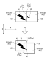
- FIG. 2 shows the combination of the first defect image C1 and the second defect image C2.
- the classification unit 10 of the defect classification device 1 classifies the pattern of the defect X in a state in which the first defect image C1 and the second defect image C2 are aligned so that the first defect X1 and the second defect X2 overlap each other.
- the first defect image C1 includes the right end 11b of the FOV 11.
- the second defect image C2 includes the left end 21d of the FOV 21. Therefore, the first defect image C1 and the second defect image C2 are aligned so that the first defect X1 and the second defect X2 overlap. Then, in the state in which the first defect image C1 and the second defect image C2 are aligned (the state in which the first defect X1 and the second defect X2 overlap), the pattern of defect X is classified.
- adjacent direction A Adjacent direction A is also the direction in which FOV11 and FOV21 overlap.
- Intersecting direction B is also a direction parallel to the right side of FOV11 and the left side of FOV21.
- the classification unit 10 of the defect classification device 1 aligns the first defect image C1 and the second defect image C2 in the adjacent direction (left-right direction) A and the intersecting direction (up-down direction) B. That is, the first defect image C1 and the second defect image C2 are aligned while being moved in the adjacent direction A and the intersecting direction B, so that the first defect X1 and the second defect X2 overlap.
- the classification unit 10 of the defect classification device 1 does not align the first defect image C1 and the second defect image C2 (does not superimpose the first defect X1 and the second defect X2). In this case, the classification unit 10 of the defect classification device 1 classifies the pattern of defect X based on the first defect image C1 alone and/or the second defect image C2 alone.
- Fig. 3 shows the overlapping of the first defect X1 and the second defect X2.
- the classification unit 10 of the defect classification device 1 cuts out a part of an area including the right end 11b (first end F1p) of the FOV 11 (first field of view F1) in the first defect image C1 as a matching image M.
- the classification unit 10 of the defect classification device 1 sets the area including the left end 21d (second end F2p) of the FOV21 (second field of view F2) in the second defect image C2 as the search range N.
- the matching image M is smaller than the first defect image C1.
- the search range N is smaller than the second defect image C2.
- the matching image M is smaller than the search range N.
- the matching image M may be cut out after the search range N is set in the reverse order to the above.
- the classification unit 10 of the defect classification device 1 extracts multiple target images T (T1, T2, ... Tn) from within the search range N set in the second defect image C2.
- Each target image T extracted from the search range N of the second defect image C2 corresponds to a matching image M extracted from the first defect image C1.
- the size of each target image T is equal to the size of the matching image M.
- the classification unit 10 of the defect classification device 1 determines the feature amount Ma of the matching image M.
- the classification unit 10 of the defect classification device 1 determines the feature amount Ta (Ta1, Ta2, ... Tan) of each of the multiple target images T (T1, T2, ... Tn).
- the classification unit 10 of the defect classification device 1 compares the feature quantity Ma of the matching image M with the feature quantities Ta (Ta1, Ta2, ... Tan) of each of the multiple target images T (T1, T2, ... Tn).
- the classification unit 10 of the defect classification device 1 determines the target image T that is closest to the matching image M among the multiple target images T as the closest target image TC.
- the classification unit 10 of the defect classification device 1 aligns the first defect image C1 and the second defect image C2 so as to overlay the matching image M on the most recent target image TC (the target image T that is closest to the matching image M among the multiple target images T).
- the classification unit 10 of the defect classification device 1 determines, among the multiple target images T, the target image T having the feature amount Ta closest to the feature amount Ma of the matching image M as the closest target image TC.
- the classification unit 10 of the defect classification device 1 superimposes the matching image M on the most recent target image TC (the target image T among the multiple target images T that has the feature value Ta closest to the feature value Ma of the matching image M).
- the SIFT Scale-Invariant Feature Transform
- the Euclidean distance between the feature vector of the matching image M and the feature vector of each target image T is calculated.
- the smaller the Euclidean distance the higher the similarity between the feature points of the matching image M and the feature points of the target image T.
- the identity of the feature points of the matching image M and the feature points of the target image T is determined.
- a portion of the area including the right end 11b of the FOV 11 in the first defect image C1 is cut out as a matching image M.
- An area including the left end 21d of the FOV 21 in the second defect image C2 is set as a search range N.
- Multiple target images T (T1, T2, ... Tn) are cut out from the search range N.
- the feature points of the matching image M are found to obtain the feature amount Ma.
- the feature points of each target image T (T1, T2, ... Tn) are found to obtain the feature amount Ta (Ta1, Ta2, ... Tan).
- the feature amount Ma of the feature points of the matching image M is matched with the feature amount Ta (Ta1, Ta2, ... Tan) of the feature points of each target image T (T1, T2, ... Tn).
- the target image T with the largest overlapping area between the feature amount Ma of the feature points of the matching image M and the feature amount Ta (Ta1, Ta2, ... Tan) of the feature points of each target image T (T1, T2, ... Tn) is obtained and designated as the nearest target image TC.
- the overlap value between the first defect image C1 and the second defect image C2 is obtained from the deviation amount between the matching image M and the nearest target image TC, and the first defect image C1 and the second defect image C2 are combined.
- the classification unit 10 of the defect classification device 1 classifies the defect X pattern in a state in which the first defect image C1 and the second defect image C2 are aligned (a state in which the first defect X1 and the second defect X2 overlap).
- the defect X pattern that has occurred in the inspected object W and straddles the right end 11b of the FOV 11 and the left end 21d of the FOV 21 is correctly classified as a "flaw.”
- the first defect image C1 extracted from the FOV11 (first field of view F1) and the second defect image C2 extracted from the FOV21 (second field of view F2) are combined such that the first defect X1 and the second defect X2 overlap each other.
- the pattern of the defect X is classified.
- the pattern of defect X occurring in the object W to be inspected can be classified with high accuracy.
- the first defect image C1 and the second defect image C2 are aligned so that the matching image M overlaps with the target image T (closest target image TC) that is closest to the matching image M among the multiple target images T. This allows the first defect X1 and the second defect X2 to be more accurately overlapped. This is advantageous in accurately classifying the pattern of the defect X that has occurred in the inspected object W.
- the first defect image C1 and the second defect image C2 can be suitably aligned in at least two directions, the adjacent direction A and the intersecting direction B.
- the defect X straddles the left-right direction between FOV11 as the first field of view F1 and FOV21 as the second field of view F2, but this is not limited to this.
- the defect X may straddle the top-bottom direction between FOV11 as the first field of view F1 and FOV12 as the second field of view F2.
- the top-bottom direction is the adjacent direction A
- the left-right direction is the intersecting direction B.
- the bottom end 11c of FOV11 is the first end F1p
- the top end 12a of FOV12 is the second end F2p.
- defect X may straddle the left-right direction between FOV12 as the first field of view F1 and FOV22 as the second field of view F2, or may straddle the top-bottom direction between FOV21 as the first field of view F1 and FOV22 as the second field of view F2.
- first field of view F1 and the second field of view F2 may be applied in reverse.
- the upper left FOV11, the lower left FOV12, the upper right FOV21, and the lower right FOV22 are exemplified as multiple fields of view F, but many other fields of view may also be included.
- the field of view F is not limited to a rectangle, but may be a polygon other than a rectangle, or a shape other than a polygon.
- the defect classification device 1 may include a judgment unit for judging whether the defect X obtained when the first defect image C1 and the second defect image C2 are aligned (when the first defect X1 and the second defect X2 overlap) appears natural.
- the classification unit 10 may not be built into the main body of the defect classification device 1, but may be provided on a server or the like that is external to the main body of the defect classification device 1.
- the object W to be inspected is not limited to a semiconductor wafer, and various objects are possible.
- the object W to be inspected may be, for example, glass, metal, resin, etc.
- the object W to be inspected does not have to be a plate material, and may be, for example, an electric wire, etc.
- This disclosure is extremely useful and has high industrial applicability because it can be applied to defect classification devices.
Landscapes
- General Physics & Mathematics (AREA)
- Physics & Mathematics (AREA)
- Immunology (AREA)
- Pathology (AREA)
- Analytical Chemistry (AREA)
- Biochemistry (AREA)
- General Health & Medical Sciences (AREA)
- Life Sciences & Earth Sciences (AREA)
- Health & Medical Sciences (AREA)
- Chemical & Material Sciences (AREA)
- Engineering & Computer Science (AREA)
- Computer Vision & Pattern Recognition (AREA)
- Theoretical Computer Science (AREA)
- Investigating Materials By The Use Of Optical Means Adapted For Particular Applications (AREA)
- Testing Or Measuring Of Semiconductors Or The Like (AREA)
- Image Analysis (AREA)
Abstract
被検査対象に発生した欠陥のパターンを精度よく分類する。 具体的には、欠陥分類装置1は、複数の視野Fに区画されるように撮像された被検査対象Wに発生した欠陥Xのパターンを分類する分類部10を備える。複数の視野は、互いに隣接した第1視野F1と第2視野F2とを含む。第1視野における第2視野側の第1端部F1pと、第2視野における第1視野側の第2端部F2pとは、互いに重なり合う。第1視野には、第1欠陥X1が含まれる。第2視野には、第2欠陥X2が含まれる。分類部は、第1視野における第1欠陥が映る領域を第1欠陥画像C1として切り出すとともに、第2視野における第2欠陥が映る領域を第2欠陥画像C2として切り出す。分類部は、第1欠陥画像が第1端部を含み且つ第2欠陥画像が第2端部を含むとき、第1欠陥と第2欠陥とが重なり合うように第1欠陥画像と第2欠陥画像とを位置合わせした状態にて、欠陥のパターンを分類する。
Description
本開示は、欠陥分類装置に関する。
例えば、半導体デバイスの製造工程では、半導体ウエハ(基板)の表面に露光、現像、エッチング等の処理を行うことによって、半導体ウエハ表面に多数の回路パターンを形成する。そして、多数の回路パターンが形成された半導体ウエハを、複数のチップ部品として個片化する。個片化されたチップ部品は、パッケージングされた後、電子部品単体として出荷されたり、電気製品に組み込まれたりする。
ここで、半導体ウエハが複数のチップ部品として個片化される前に、半導体ウエハ表面に対して、欠陥の検出が行われる。欠陥の検出は、例えば、光学顕微鏡や走査電子顕微鏡に接続されたカメラにより撮像された検査画像に基づいて、行われる。
そして、欠陥の検出された半導体ウエハに対して、欠陥の形状やサイズや色などの特徴量に基づいて、欠陥パターンの分類が行われる。欠陥パターンとして、例えば、異物や傷などがある。
従来、欠陥パターンの分類は、作業者による目視検査によって行われてきた。しかしながら、目視検査では、作業者の主観に応じて、欠陥パターンの分類結果にバラツキが生じ得るので、欠陥パターンを精度よく分類することができなかった。
そこで、特許文献1に示すように、半導体ウエハ表面に発生した欠陥パターンを自動的に分類する自動欠陥分類装置(Automatic Defect Classification:ADC)が、知られている。
しかしながら、特許文献1に係る自動欠陥分類装置を用いて、作業者の主観を排して欠陥パターンを分類したとしても、依然として、欠陥パターンの分類精度に課題がある。
被検査対象である半導体ウエハは、通常、カメラの視野(撮像範囲)よりも大きい。そこで、半導体ウエハを複数の視野に区画してカメラで撮像することによって、複数の視野毎に検査画像を得る。このとき、半導体ウエハに発生した欠陥が、複数の視野に亘って跨ることがある。
このため、1つの視野のみに基づいて欠陥パターンを分類しようとすると、欠陥パターンを正確に分類できないことがある。例えば、当該1つの視野の端部に僅かに一部だけ欠陥が映っている場合、一部だけ映された欠陥の本来の特徴量(形状やサイズや色など)を十分に把握できないので、正確な欠陥パターンを把握することができない。
上記課題は、半導体ウエハ以外の他の被検査対象にも、当てはまる。
本開示は斯かる点に鑑みてなされたものであり、その目的とするところは、被検査対象に発生した欠陥のパターンを精度よく分類することにある。
本開示に係る欠陥分類装置は、複数の視野に区画されるように撮像された被検査対象に発生した欠陥のパターンを分類する分類部を備え、複数の前記視野は、互いに隣接した第1視野と第2視野とを含み、前記第1視野における前記第2視野側の端部である第1端部と、前記第2視野における前記第1視野側の端部である第2端部とは、互いに重なり合い、前記第1視野には、前記欠陥としての第1欠陥が含まれ、前記第2視野には、前記欠陥としての第2欠陥が含まれ、前記分類部は、前記第1視野における前記第1欠陥が映る領域を第1欠陥画像として切り出すとともに、前記第2視野における前記第2欠陥が映る領域を第2欠陥画像として切り出し、前記分類部は、前記第1欠陥画像が前記第1端部を含み且つ前記第2欠陥画像が前記第2端部を含むとき、前記第1欠陥と前記第2欠陥とが重なり合うように前記第1欠陥画像と前記第2欠陥画像とを位置合わせした状態にて、前記欠陥のパターンを分類する。
本実施形態によれば、第1視野から切り出された第1欠陥画像と、第2視野から切り出された第2欠陥画像とは、第1欠陥と第2欠陥とが重なり合うように、結合される。第1欠陥画像と第2欠陥画像とが結合した状態にて、欠陥のパターンが分類される。
被検査対象に発生した欠陥が第1視野と第2視野とに亘って跨っている場合であっても、欠陥の本来の特徴量を把握することができる。
以上、被検査対象に発生した欠陥のパターンを精度よく分類することができる。
一実施形態では、前記分類部は、前記第1欠陥画像における前記第1端部を含む領域をマッチング画像として切り出すとともに、前記第2欠陥画像における前記第2端部を含む領域を探索範囲として設定し、前記分類部は、前記探索範囲の中から前記マッチング画像に対応する複数のターゲット画像を切り出し、前記分類部は、複数の前記ターゲット画像のうちの、前記マッチング画像に最も近い前記ターゲット画像に対して、前記マッチング画像を重ね合わせるように、前記第1欠陥画像と前記第2欠陥画像とを位置合わせする。
かかる構成によれば、複数のターゲット画像Tのうちの、マッチング画像に最も近いターゲット画像に対して、マッチング画像が重なり合うように、第1欠陥画像と第2欠陥画像とを位置合わせすることによって、第1欠陥と第2欠陥とをより正しく重ね合わせることができる。これにより、被検査対象に発生した欠陥のパターンを精度よく分類する上で、有利になる。
一実施形態では、前記分類部は、前記マッチング画像の特徴量を求めるとともに、複数の前記ターゲット画像それぞれの特徴量を求め、前記分類部は、前記マッチング画像の特徴量と複数の前記ターゲット画像それぞれの特徴量とを比較し、前記分類部は、複数の前記ターゲット画像のうちの、前記マッチング画像の特徴量と最も近い特徴量を有する前記ターゲット画像に対して、前記マッチング画像を重ね合わせる。
かかる構成によれば、マッチング画像の特徴量と複数のターゲット画像それぞれの特徴量とを比較することによって、複数のターゲット画像の中からマッチング画像に最も近いターゲット画像を、より精度よく判定することができる。
一実施形態では、前記分類部は、前記第1視野と前記第2視野とが隣接する隣接方向、及び前記隣接方向に交差する交差方向において、前記第1欠陥画像と前記第2欠陥画像とを位置合わせする。
かかる構成によれば、第1欠陥画像と第2欠陥画像とを、隣接方向及び交差方向の少なくとも2方向において、好適に位置合わせすることができる。
本開示によれば、被検査対象に発生した欠陥のパターンを精度よく分類することができる。
以下、本開示の一実施形態を図面に基づいて詳細に説明する。以下の好ましい実施形態の説明は、本質的に例示に過ぎず、本開示、その適用物あるいはその用途を制限することを意図するものでは全くない。
(欠陥分類)
図1は、欠陥分類装置1による欠陥分類方法を模式的に示す。欠陥分類装置1は、自動欠陥分類装置(Automatic Defect Classification:ADC)である。欠陥分類装置1は、分類部10を備える。分類部10は、欠陥分類装置1本体に内蔵されている。分類部10は、例えばコンピュータである。分類部10は、例えば、基板上に搭載されたプロセッサと、プロセッサを動作させるためのソフトウエアを格納するメモリデバイスと、を含む。
図1は、欠陥分類装置1による欠陥分類方法を模式的に示す。欠陥分類装置1は、自動欠陥分類装置(Automatic Defect Classification:ADC)である。欠陥分類装置1は、分類部10を備える。分類部10は、欠陥分類装置1本体に内蔵されている。分類部10は、例えばコンピュータである。分類部10は、例えば、基板上に搭載されたプロセッサと、プロセッサを動作させるためのソフトウエアを格納するメモリデバイスと、を含む。
欠陥分類装置1の分類部10は、被検査対象Wに発生した欠陥Xのパターンを、分類する。本例では、被検査対象Wは、半導体製造工程における半導体ウエハ(基板)の表面である。
欠陥分類装置1による欠陥Xのパターンの分類工程よりも前工程において、欠陥検出装置(図示せず)による欠陥Xの検出が行われる。欠陥Xの検出にあたって、光学顕微鏡や走査電子顕微鏡に接続されたカメラ(図示せず)によって被検査対象Wを撮像して検査画像Jを得るとともに、検査画像Jを基準画像Kと比較する。
基準画像Kは、フィッティング画像や統計的良品画像とも呼ばれる。基準画像Kは、例えば、良品判定された被検査対象Wの画像を平均化することによって、得られる。基準画像Kは、事前に設定されている。欠陥Xの検出にあたって、検査画像Jを、基準画像Kに重ね合わせる。
欠陥分類装置1の分類部10は、欠陥検出装置により欠陥Xが検出された被検査対象Wについてのみ、欠陥Xのパターンを分類する。ここで、欠陥Xのパターンとして、例えば、異物、傷、エッジリンス不良、スルーホール異常、塗膜ムラ、剥がれ、スクラッチ、ボンディングパッド異常、色ムラ、パターン異常、染み、変色、変形、などがある。
欠陥分類装置1の分類部10は、被検査対象Wの検査画像Jに対して、欠陥Xにおける所定の特徴量に基づいて、欠陥Xのパターンを分類する。
欠陥Xの特徴量として、例えば、面積、明るさ、色、輝度、形状、鮮明さ、長さ、幅、幅/長さ、角度、透明度、などがある。欠陥分類装置1の分類部10には、欠陥Xの特徴量が、事前に登録されている。
欠陥分類装置1の分類部10は、被検査対象Wの検査画像Jに対して、AI(Artificial Intelligence)学習により生成された分類条件に基づいて、欠陥Xのパターンを分類してもよい。AI学習として、例えば、機械学習やディープラーニング等がある。また、機械学習として、「教師有り学習」、「教師無し学習」及び「強化学習」等がある。
(視野の区画)
ここで、被検査対象Wは、通常、カメラの視野(撮像範囲)Fよりも大きい。そこで、被検査対象Wは、複数の視野Fに区画されるように、撮像される。これにより、複数の視野F毎に検査画像Jが得られる。
ここで、被検査対象Wは、通常、カメラの視野(撮像範囲)Fよりも大きい。そこで、被検査対象Wは、複数の視野Fに区画されるように、撮像される。これにより、複数の視野F毎に検査画像Jが得られる。
各視野F(各検査画像J)は、互いに隣接している。本例では、各視野Fは、四角形である。各視野Fは、四角形の格子状に並んでいる。換言すると、各視野Fは、上下左右に互いに隣接している。各視野Fは、さらに複数の画素に区画されている。
以下、視野FをFOV(field of view)という場合がある。
図1では、複数の視野Fとして、左上のFOV11と、左下のFOV12と、右上のFOV21と、右下のFOV22と、を例示する。
FOV11とFOV12とは、上下方向に隣接している。FOV11におけるFOV12側の端部である下端部11cと、FOV12におけるFOV11側の端部である上端部12aとは、互いに重なり合っている(オーバラップしている)。
FOV11とFOV21とは、左右方向に隣接している。FOV11におけるFOV21側の端部である右端部11bと、FOV21におけるFOV11側の端部である左端部21dとは、互いに重なり合っている(オーバラップしている)。
FOV21とFOV22とは、上下方向に隣接している。FOV21におけるFOV22側の端部である下端部21cと、FOV22におけるFOV21側の端部である上端部22aとは、互いに重なり合っている(オーバラップしている)。
FOV12とFOV22とは、左右方向に隣接している。FOV12におけるFOV22側の端部である右端部12bと、FOV22におけるFOV12側の端部である左端部22dとは、互いに重なり合っている(オーバラップしている)。
上述の「端部」は、視野Fにおける端及び端からやや内側の領域を含む。
カメラによって、4つの視野F(FOV11,FOV12,FOV21,FOV22)に対応するように、4つの検査画像J11,J12,J21,J22が得られる。
基準画像Kも、検査画像Jと同様である。すなわち、4つの視野F(FOV11,FOV12,FOV21,FOV22)に対応するように、4つの基準画像K11,K12,K21,K22が予め用意されている。
ここで、被検査対象Wに発生した欠陥Xが、複数の視野F(検査画像J)に亘って跨ることがある。図1の例では、被検査対象Wに発生した欠陥Xは、FOV11(検査画像J11)とFOV21(検査画像J21)とに亘って左右方向に跨っている。
図1に示すように、欠陥Xは、FOV11(検査画像J11)における中間部から右端部11bまで延びた後に、FOV21(検査画像J21)における左端部21dに至っている。欠陥Xには、ノコギリの歯のようなギザギザの形状がある。
ここで、欠陥検出装置は、被検査対象WにおけるFOV11(検査画像J11)及びFOV21(検査画像J21)において、欠陥Xを検出する。一方、欠陥検出装置は、被検査対象WにおけるFOV12(検査画像J12)及びFOV22(検査画像J22)において、欠陥Xを検出しない。なお、4つの基準画像K11,K12,K21,K22のいずれにも、欠陥Xは存在しない。
欠陥分類装置1による欠陥Xのパターンの分類では、欠陥検出装置により欠陥Xの検出された視野F(検査画像J)のみを、抽出して、基準画像Kと比較する。図1の例では、欠陥Xの検出された視野F(検査画像J)として、FOV11(検査画像J11)及びFOV21(検査画像J21)が、先ず抽出される。そして、FOV11(検査画像J11)が基準画像K11と比較されるとともに、FOV21(検査画像J21)が基準画像K21と比較される。
1つの視野Fのみに基づいて欠陥Xのパターンを分類しようとすると、欠陥Xのパターンを正確に分類できないことがある。例えば、FOV21(検査画像J21)には、その左端部21d付近に僅かにしか欠陥Xが映っていない。このため、FOV21(検査画像J21)を基準画像K22と比較したとしても、欠陥Xの本来の特徴量(形状やサイズや色など)を十分に把握できず、正確な欠陥Xのパターンを把握することができない。
一方、FOV11(検査画像J11)には、その中間部から右端部11bに亘って大部分で欠陥Xが映っている。このため、FOV11(検査画像J11)を基準画像K11と比較した場合、欠陥Xの本来の特徴量を把握できるかもしれず、正確な欠陥Xのパターンを把握できるかもしれない。例えば、FOV11(検査画像J11)に映る欠陥Xにおけるギザギザの形状に基づいて、欠陥Xのパターンを「傷」と分類できるかもしれない。
しかしながら、仮に、FOV11(検査画像J11)にも、FOV21(検査画像J21)と同様に僅かにしか欠陥Xが映っていなければ、やはり欠陥Xの本来の特徴量を把握できず、正確な欠陥Xのパターンを把握できないであろう。
このように、被検査対象Wに発生した欠陥Xが複数の視野F(検査画像J)に亘って跨る場合に、欠陥Xのパターンを精度よく分類することは難しい。
本実施形態に係る欠陥分類装置1では、以下の工夫を施すことによって、被検査対象Wに発生した欠陥Xが複数の視野F(検査画像J)に亘って跨る場合であっても、欠陥Xのパターンを精度よく分類することを可能にした。
(欠陥画像の切り出し)
以下、FOV11を第1視野F1とする。FOV21を第2視野F2とする。図1に示すように、複数の視野Fは、第1視野F1としてのFOV11と、第2視野F2としてのFOV21と、を含む。FOV11(第1視野F1)とFOV21(第2視野F2)とは、左右方向に互いに隣接している。
以下、FOV11を第1視野F1とする。FOV21を第2視野F2とする。図1に示すように、複数の視野Fは、第1視野F1としてのFOV11と、第2視野F2としてのFOV21と、を含む。FOV11(第1視野F1)とFOV21(第2視野F2)とは、左右方向に互いに隣接している。
FOV11(第1視野F1)におけるFOV21(第2視野F2)側の端部である第1端部F1pとしての右端部11bと、FOV21(第2視野F2)におけるFOV11(第1視野F1)側の端部である第2端部F2pとしての左端部21dとは、互いに重なり合っている(オーバラップしている)。
FOV11(第1視野F1)の右端部11b(第1端部F1p)は、FOV11(第1視野F1)における右端及び右端からやや左側の領域を含む。FOV21(第2視野F2)の左端部21d(第2端部F2p)は、FOV21(第2視野F2)における左端及び左端からやや右側の領域を含む。
FOV11(第1視野F1)におけるFOV21(第2視野F2)側の端である右端は、FOV21(第2視野F2)の左端よりも、FOV21(第2視野F2)寄りである右寄りに位置する。FOV21(第2視野F2)におけるFOV11(第1視野F1)側の端である左端は、FOV11(第1視野F1)の右端よりも、FOV11(第1視野F1)寄りである左寄りに位置する。
図1に示すように、FOV11(第1視野F1)には、欠陥Xとしての第1欠陥X1が含まれる。FOV21(第2視野F2)には、欠陥Xとしての第2欠陥X2が含まれる。第1欠陥X1は、欠陥Xの一部である。第2欠陥X2は、欠陥Xの一部である。
図1に示すように、欠陥分類装置1の分類部10は、FOV11(第1視野F1)における第1欠陥X1が映る領域を、第1欠陥画像C1として切り出す。欠陥分類装置1の分類部10は、FOV21(第2視野F2)における第2欠陥X2が映る領域を、第2欠陥画像C2として切り出す。
第1欠陥画像C1は、FOV11(第1視野F1)よりも小さい。第2欠陥画像C2は、FOV21(第2視野F2)よりも小さい。第1欠陥画像C1は、第1欠陥X1が視認しやすくなるように、サイズ及び位置が設定される。第2欠陥画像C2は、第2欠陥X2が視認しやすくなるように、サイズ及び位置が設定される。第1欠陥画像C1のサイズ及び位置と第2欠陥画像C2のサイズ及び位置とは、互いに同じこともあれば、互いに異なることもある。
(欠陥画像の結合)
第1欠陥画像C1と第2欠陥画像C2との結合について、詳細に説明する。図2は、第1欠陥画像C1と第2欠陥画像C2との結合を示す。欠陥分類装置1の分類部10は、第1欠陥画像C1がFOV11(第1視野F1)の右端部11b(第1端部F1p)を含み且つ第2欠陥画像C2がFOV21(第2視野F2)の左端部21d(第2端部F2p)を含むとき、第1欠陥X1と第2欠陥X2とが重なり合うように第1欠陥画像C1と第2欠陥画像C2とを位置合わせした状態にて、欠陥Xのパターンを分類する。
第1欠陥画像C1と第2欠陥画像C2との結合について、詳細に説明する。図2は、第1欠陥画像C1と第2欠陥画像C2との結合を示す。欠陥分類装置1の分類部10は、第1欠陥画像C1がFOV11(第1視野F1)の右端部11b(第1端部F1p)を含み且つ第2欠陥画像C2がFOV21(第2視野F2)の左端部21d(第2端部F2p)を含むとき、第1欠陥X1と第2欠陥X2とが重なり合うように第1欠陥画像C1と第2欠陥画像C2とを位置合わせした状態にて、欠陥Xのパターンを分類する。
本例では、第1欠陥画像C1は、FOV11の右端部11bを含む。第2欠陥画像C2は、FOV21の左端部21dを含む。このため、第1欠陥画像C1と第2欠陥画像C2とは、第1欠陥X1と第2欠陥X2とが重なり合うように、位置合わせされる。そして、第1欠陥画像C1と第2欠陥画像C2とが位置合わせされた状態(第1欠陥X1と第2欠陥X2とが重なり合った状態)にて、欠陥Xのパターンが分類される。
ここで、FOV11(第1視野F1)とFOV21(第2視野F2)とが隣接する左右方向を、隣接方向Aとする。隣接方向Aは、FOV11とFOV21とが重なり合う(オーバラップする)方向でもある。左右方向である隣接方向Aに交差(詳細には直交)する上下方向を、交差方向Bとする。交差方向Bは、FOV11の右辺及びFOV21の左辺に対して平行な方向でもある。
欠陥分類装置1の分類部10は、隣接方向(左右方向)A及び交差方向(上下方向)Bにおいて、第1欠陥画像C1と第2欠陥画像C2とを位置合わせする。すなわち、第1欠陥画像C1と第2欠陥画像C2とは、隣接方向A及び交差方向Bに動かされながら、第1欠陥X1と第2欠陥X2とが重なり合うように、位置合わせされる。
逆に、欠陥分類装置1の分類部10は、第1欠陥画像C1がFOV11(第1視野F1)の右端部11b(第1端部F1p)を含まない又は第2欠陥画像C2がFOV21(第2視野F2)の左端部21d(第2端部F2p)を含まないとき、第1欠陥画像C1と第2欠陥画像C2とを位置合わせしない(第1欠陥X1と第2欠陥X2とを重ね合わせない)。この場合、欠陥分類装置1の分類部10は、第1欠陥画像C1単体及び/又は第2欠陥画像C2単体に基づいて、欠陥Xのパターンを分類する。
(第1欠陥と第2欠陥との重ね合わせ)
第1欠陥X1と第2欠陥X2との重ね合わせについて、詳細に説明する。図3は、第1欠陥X1と第2欠陥X2との重ね合わせを示す。欠陥分類装置1の分類部10は、第1欠陥画像C1におけるFOV11(第1視野F1)の右端部11b(第1端部F1p)を含む領域の一部をマッチング画像Mとして切り出す。
第1欠陥X1と第2欠陥X2との重ね合わせについて、詳細に説明する。図3は、第1欠陥X1と第2欠陥X2との重ね合わせを示す。欠陥分類装置1の分類部10は、第1欠陥画像C1におけるFOV11(第1視野F1)の右端部11b(第1端部F1p)を含む領域の一部をマッチング画像Mとして切り出す。
次に、欠陥分類装置1の分類部10は、第2欠陥画像C2におけるFOV21(第2視野F2)の左端部21d(第2端部F2p)を含む領域を探索範囲Nとして設定する。
マッチング画像Mは、第1欠陥画像C1よりも小さい。探索範囲Nは、第2欠陥画像C2よりも小さい。マッチング画像Mは、探索範囲Nよりも小さい。上記とは逆の順序で、探索範囲Nの設定の後に、マッチング画像Mの切り出しを行ってもよい。
欠陥分類装置1の分類部10は、第2欠陥画像C2に設定された探索範囲Nの中から、複数のターゲット画像T(T1,T2,…Tn)を切り出す。第2欠陥画像C2の探索範囲Nから切り出された各ターゲット画像Tは、第1欠陥画像C1から切り出されたマッチング画像Mに対応している。各ターゲット画像Tのサイズは、マッチング画像Mのサイズに等しい。
欠陥分類装置1の分類部10は、マッチング画像Mの特徴量Maを求める。欠陥分類装置1の分類部10は、複数のターゲット画像T(T1,T2,…Tn)それぞれの特徴量Ta(Ta1,Ta2,…Tan)を求める。
欠陥分類装置1の分類部10は、マッチング画像Mの特徴量Maと複数のターゲット画像T(T1,T2,…Tn)それぞれの特徴量Ta(Ta1,Ta2,…Tan)とを比較する。
欠陥分類装置1の分類部10は、複数のターゲット画像Tのうちの、マッチング画像Mに最も近いターゲット画像Tを、最近ターゲット画像TCとする。
欠陥分類装置1の分類部10は、最近ターゲット画像TC(複数のターゲット画像Tのうちのマッチング画像Mに最も近いターゲット画像T)に対してマッチング画像Mを重ね合わせるように、第1欠陥画像C1と第2欠陥画像C2とを位置合わせする。
詳細には、欠陥分類装置1の分類部10は、複数のターゲット画像Tのうちの、マッチング画像Mの特徴量Maと最も近い特徴量Taを有するターゲット画像Tを、最近ターゲット画像TCとする。
欠陥分類装置1の分類部10は、最近ターゲット画像TC(複数のターゲット画像Tのうちの、マッチング画像Mの特徴量Maと最も近い特徴量Taを有するターゲット画像T)に対して、マッチング画像Mを重ね合わせる。
マッチング画像Mの特徴量Maと各ターゲット画像Tの特徴量Taとを比較するに際して、例えば、SIFT(Scale-Invariant Feature Transform)法が用いられる。マッチング画像Mから特徴点を検出する。マッチング画像Mの特徴点の周辺領域における特徴ベクトルを求める。各ターゲット画像Tから特徴点を検出する。各ターゲット画像Tの特徴点の周辺領域における特徴ベクトルを求める。
マッチング画像Mの特徴ベクトルと各ターゲット画像Tの特徴ベクトルとのユークリッド距離を計算する。当該ユークリッド距離が小さいほど、マッチング画像Mの特徴点とターゲット画像Tの特徴点との類似性が高くなるとして、マッチング画像Mの特徴点とのターゲット画像Tの特徴点との同一性を判定する。
本例に当てはめると、第1欠陥画像C1におけるFOV11の右端部11bを含む領域の一部をマッチング画像Mとして切り出す。第2欠陥画像C2におけるFOV21の左端部21dを含む領域を探索範囲Nとして設定する。探索範囲Nの中から、複数のターゲット画像T(T1,T2,…Tn)を切り出す。
マッチング画像Mの特徴点を求めて特徴量Maを得る。各ターゲット画像T(T1,T2,…Tn)の特徴点を求めて特徴量Ta(Ta1,Ta2,…Tan)を得る。
マッチング画像Mの特徴点の特徴量Maと各ターゲット画像T(T1,T2,…Tn)の特徴点の特徴量Ta(Ta1,Ta2,…Tan)とをマッチングする。マッチング画像Mの特徴点の特徴量Maと各ターゲット画像T(T1,T2,…Tn)の特徴点の特徴量Ta(Ta1,Ta2,…Tan)との重なり領域面積が最も大きいターゲット画像Tを求めて、最近ターゲット画像TCとする。マッチング画像Mと最近ターゲット画像TCとのずれ量から、第1欠陥画像C1と第2欠陥画像C2とのオーバラップ値を求めて、第1欠陥画像C1と第2欠陥画像C2とを結合する。
このようにして、欠陥分類装置1の分類部10は、第1欠陥画像C1と第2欠陥画像C2とが位置合わせされた状態(第1欠陥X1と第2欠陥X2とが重なり合った状態)にて、欠陥Xのパターンを分類する。これにより、FOV11の右端部11bとFOV21の左端部21dとに跨るようにして、被検査対象Wに発生した欠陥Xのパターンは、「傷」と正しく分類される。
(作用効果)
FOV11(第1視野F1)から切り出された第1欠陥画像C1と、FOV21(第2視野F2)から切り出された第2欠陥画像C2とは、第1欠陥X1と第2欠陥X2とが重なり合うように、結合される。第1欠陥画像C1と第2欠陥画像C2とが結合した状態にて、欠陥Xのパターンが分類される。
FOV11(第1視野F1)から切り出された第1欠陥画像C1と、FOV21(第2視野F2)から切り出された第2欠陥画像C2とは、第1欠陥X1と第2欠陥X2とが重なり合うように、結合される。第1欠陥画像C1と第2欠陥画像C2とが結合した状態にて、欠陥Xのパターンが分類される。
被検査対象Wに発生した欠陥XがFOV11(第1視野F1)とFOV21(第2視野F2)とに亘って跨っている場合であっても、欠陥Xの本来の特徴量を把握することができる。
以上、被検査対象Wに発生した欠陥Xのパターンを精度よく分類することができる。
FOV11とFOV21とを直接的に結合するのではなく、FOV11から切り出された第1欠陥画像C1とFOV21から切り出された第2欠陥画像C2とを結合することによって、欠陥分類装置1の分類部10に保存される画像の容量を節約できる。
複数のターゲット画像Tのうちの、マッチング画像Mに最も近いターゲット画像T(最近ターゲット画像TC)に対して、マッチング画像Mが重なり合うように、第1欠陥画像C1と第2欠陥画像C2とを位置合わせする。これによって、第1欠陥X1と第2欠陥X2とを、より正しく重ね合わせることができる。そして、被検査対象Wに発生した欠陥Xのパターンを精度よく分類する上で、有利になる。
マッチング画像Mの特徴量Maと複数のターゲット画像Tそれぞれの特徴量Taとを比較することによって、複数のターゲット画像Tの中からマッチング画像Mに最も近いターゲット画像T(最近ターゲット画像TC)を、より精度よく判定することができる。
第1欠陥画像C1と第2欠陥画像C2とを、隣接方向A及び交差方向Bの少なくとも2方向において、好適に位置合わせすることができる。
(その他の実施形態)
以上、本開示を好適な実施形態により説明してきたが、こうした記述は限定事項ではなく、勿論、種々の改変、置換又は組合せが可能である。
以上、本開示を好適な実施形態により説明してきたが、こうした記述は限定事項ではなく、勿論、種々の改変、置換又は組合せが可能である。
上記実施形態では、欠陥Xが、第1視野F1としてのFOV11と第2視野F2としてのFOV21との間に亘って左右方向に跨っているが、これに限定されない。例えば、欠陥Xは、第1視野F1としてのFOV11と第2視野F2としてのFOV12との間に亘って上下方向に跨ってもよい。この場合、上下方向が隣接方向Aとなり、左右方向が交差方向Bとなる。また、FOV11の下端部11cが第1端部F1pとなり、FOV12の上端部12aが第2端部F2pとなる。
他にも、欠陥Xは、第1視野F1としてのFOV12と第2視野F2としてのFOV22との間に亘って左右方向に跨ったり、第1視野F1としてのFOV21と第2視野F2としてのFOV22との間に亘って上下方向に跨ったりしてもよい。
上で例示したケースに対して、第1視野F1と第2視野F2とを逆に適用してもよい。
「第1…」及び「第2…」は、明細書での説明の便宜上の理由で、名付けたにすぎない。
上記実施形態では、複数の視野Fとして、左上のFOV11と左下のFOV12と右上のFOV21と右下のFOV22とを例示したが、他にも多数の視野が含まれてもよい。
視野Fは、四角形に限定されず、四角形以外の多角形や、多角形以外の形状などでもよい。
欠陥分類装置1は、第1欠陥画像C1と第2欠陥画像C2とが位置合わせされた状態(第1欠陥X1と第2欠陥X2とが重なり合った状態)で得られる欠陥Xが自然な見え方であるかを判定するため判定部を、備えてもよい。
マッチング画像Mの特徴量Maと各ターゲット画像Tの特徴量Taとを比較するに際して、SIFT法の代わりに、他の方法(例えば機械学習モデルを用いた方法など)を適用してもよい。
分類部10は、欠陥分類装置1本体に内蔵されるのではなく、欠陥分類装置1本体の外部にあるサーバなどに設けられてもよい。
被検査対象Wは、半導体ウエハに限定されず、種々の対象が考えられ得る。被検査対象Wは、例えば、ガラスや金属や樹脂等でもよい。被検査対象Wは、板材でなくてもよく、例えば電線等でもよい。
本開示は、欠陥分類装置に適用できるので、極めて有用であり、産業上の利用可能性が高い。
W 被検査対象
X 欠陥
X1 第1欠陥
X2 第2欠陥
J 検査画像
K 基準画像
F 視野
FOV11
F1 第1視野
FOV21
F2 第2視野
11b 右端部
F1p 第1端部
21d 左端部
F2p 第2端部
C1 第1欠陥画像
C2 第2欠陥画像
A 隣接方向
B 交差方向
M マッチング画像
N 探索範囲
T ターゲット画像
TC 最近ターゲット画像
Ma 特徴量
Ta 特徴量
1 欠陥分類装置
10 分類部
X 欠陥
X1 第1欠陥
X2 第2欠陥
J 検査画像
K 基準画像
F 視野
FOV11
F1 第1視野
FOV21
F2 第2視野
11b 右端部
F1p 第1端部
21d 左端部
F2p 第2端部
C1 第1欠陥画像
C2 第2欠陥画像
A 隣接方向
B 交差方向
M マッチング画像
N 探索範囲
T ターゲット画像
TC 最近ターゲット画像
Ma 特徴量
Ta 特徴量
1 欠陥分類装置
10 分類部
Claims (11)
- [引用による補充(規則20.6)05.12.2024]
複数の視野に区画されるように撮像された被検査対象に発生した欠陥のパターンを分類する分類部を備え、
複数の前記視野は、互いに隣接した第1視野と第2視野とを含み、
前記第1視野における前記第2視野側の端部である第1端部と、前記第2視野における前記第1視野側の端部である第2端部とは、互いに重なり合い、
前記第1視野には、前記欠陥としての第1欠陥が含まれ、
前記第2視野には、前記欠陥としての第2欠陥が含まれ、
前記分類部は、前記第1視野における前記第1欠陥が映る領域を第1欠陥画像として切り出すとともに、前記第2視野における前記第2欠陥が映る領域を第2欠陥画像として切り出し、
前記分類部は、前記第1欠陥画像が前記第1端部を含み且つ前記第2欠陥画像が前記第2端部を含むとき、前記第1欠陥と前記第2欠陥とが重なり合うように前記第1欠陥画像と前記第2欠陥画像とを位置合わせした状態にて、前記欠陥のパターンを分類する、欠陥分類装置。 - [引用による補充(規則20.6)05.12.2024]
前記分類部は、前記第1欠陥画像における前記第1端部を含む領域をマッチング画像として切り出すとともに、前記第2欠陥画像における前記第2端部を含む領域を探索範囲として設定し、
前記分類部は、前記探索範囲の中から前記マッチング画像に対応する複数のターゲッ卜画像を切り出し、
前記分類部は、複数の前記ターゲット画像のうちの前記マッチング画像に最も近い前記ターゲット画像に対して、前記マッチング画像を重ね合わせるように、前記第1欠陥画像と前記第2欠陥画像とを位置合わせする、請求項1に記載の欠陥分類装置。 - [引用による補充(規則20.6)05.12.2024]
前記分類部は、前記マッチング画像の特徴量を求めるとともに、複数の前記ターゲッ卜画像それぞれの特徴量を求め、
前記分類部は、前記マッチング画像の特徴量と複数の前記ターゲット画像それぞれの特徴量とを比較し、
前記分類部は、複数の前記ターゲット画像のうちの、前記マッチング画像の特徴量と最も近い特徴量を有する前記ターゲット画像に対して、前記マッチング画像を重ね合わせる、請求項2に記載の欠陥分類装置。 - [引用による補充(規則20.6)05.12.2024]
前記分類部は、前記第1視野と前記第2視野とが隣接する隣接方向、及び前記隣接方向に交差する交差方向において、前記第1欠陥画像と前記第2欠陥画像とを位置合わせする、請求項1から3のいずれか1つに記載の欠陥分類装置。 - [誤った提出(規則20.5の2)]
基板を保持するステージを備え、
前記ステージは、前記基板が載置される載置面と、前記載置面に設けられた凹部で形成され且つ同心状に配置された複数の吸着溝と、を含み、
前記吸着溝は、負圧によって前記基板を吸着し、
前記載置面は、前記吸着溝を横切る境界部を含み、
前記吸着溝は、前記境界部で分割されている、基板保持装置。 - [誤った提出(規則20.5の2)]
前記基板のエッジを前記吸着溝に合わせることによって、前記基板が前記ステージに位置決めされる、請求項1に記載の基板保持装置。 - [誤った提出(規則20.5の2)]
前記基板の寸法に基づいて、同心状に配置された複数の前記吸着溝の中から、前記基板の前記エッジを合わせるべき前記吸着溝を、判定する判定部を備える、請求項2に記載の基板保持装置。 - [誤った提出(規則20.5の2)]
前記吸着溝の気体を吸引する負圧ポンプと、
前記負圧ポンプと前記吸着溝との間での前記気体の通路を開閉する複数のバルブと、
判定部と、を備え、
前記バルブは、同心状に配置された複数の前記吸着溝毎に、前記吸着溝における前記境界部で分割された部分の両方に、それぞれ対応しており、
前記判定部は、前記基板の寸法に基づいて、複数の前記バルブの中から、開くべき前記バルブを判定する、請求項1から3のいずれか1つ記載の基板保持装置。 - [誤った提出(規則20.5の2)]
前記ステージは、同心状に配置された複数の前記吸着溝とは同心にならない位置に、前記境界部で分割されない非分割吸着溝を含み、
前記非分割吸着溝は、負圧によって前記基板を吸着する、請求項1から3のいずれか1つに記載の基板保持装置。 - [誤った提出(規則20.5の2)]
前記ステージは、前記載置面に設けられた凹部で形成され且つ前記吸着溝に隣り合う隣接溝を含む、請求項1から3のいずれか1つに記載の基板保持装置。 - [誤った提出(規則20.5の2)]
前記吸着溝は、四角形状である、請求項1から3のいずれか1つに記載の基板保持装置。
Applications Claiming Priority (2)
| Application Number | Priority Date | Filing Date | Title |
|---|---|---|---|
| JP2023-214903 | 2023-12-20 | ||
| JP2023214903A JP2025098638A (ja) | 2023-12-20 | 2023-12-20 | 欠陥分類装置 |
Publications (1)
| Publication Number | Publication Date |
|---|---|
| WO2025134591A1 true WO2025134591A1 (ja) | 2025-06-26 |
Family
ID=96136701
Family Applications (1)
| Application Number | Title | Priority Date | Filing Date |
|---|---|---|---|
| PCT/JP2024/039882 Pending WO2025134591A1 (ja) | 2023-12-20 | 2024-11-08 | 欠陥分類装置 |
Country Status (2)
| Country | Link |
|---|---|
| JP (1) | JP2025098638A (ja) |
| WO (1) | WO2025134591A1 (ja) |
Citations (3)
| Publication number | Priority date | Publication date | Assignee | Title |
|---|---|---|---|---|
| JP2000022934A (ja) * | 1998-07-03 | 2000-01-21 | Sharp Corp | 画像処理装置 |
| WO2011007516A1 (ja) * | 2009-07-17 | 2011-01-20 | 株式会社日立ハイテクノロジーズ | 走査型電子顕微鏡装置及びそれを用いたパターン寸法の計測方法 |
| JP2022055953A (ja) * | 2020-09-29 | 2022-04-08 | タカノ株式会社 | 欠陥分類装置、欠陥分類方法及びプログラム |
-
2023
- 2023-12-20 JP JP2023214903A patent/JP2025098638A/ja active Pending
-
2024
- 2024-11-08 WO PCT/JP2024/039882 patent/WO2025134591A1/ja active Pending
Patent Citations (3)
| Publication number | Priority date | Publication date | Assignee | Title |
|---|---|---|---|---|
| JP2000022934A (ja) * | 1998-07-03 | 2000-01-21 | Sharp Corp | 画像処理装置 |
| WO2011007516A1 (ja) * | 2009-07-17 | 2011-01-20 | 株式会社日立ハイテクノロジーズ | 走査型電子顕微鏡装置及びそれを用いたパターン寸法の計測方法 |
| JP2022055953A (ja) * | 2020-09-29 | 2022-04-08 | タカノ株式会社 | 欠陥分類装置、欠陥分類方法及びプログラム |
Also Published As
| Publication number | Publication date |
|---|---|
| JP2025098638A (ja) | 2025-07-02 |
Similar Documents
| Publication | Publication Date | Title |
|---|---|---|
| JP6618478B2 (ja) | 射影画像を用いた自動インライン検査及び計測 | |
| US8538168B2 (en) | Image pattern matching systems and methods for wafer alignment | |
| CN110517969B (zh) | 晶圆缺陷监测方法及系统和计算机存储介质 | |
| KR102557190B1 (ko) | 설계를 사용한 사전 층 결함 사이트 검토 | |
| US7953269B2 (en) | Method for inspecting pattern defect occured on patterns formed on a substrate | |
| WO2008008817A2 (en) | Edge inspection and metrology | |
| JP2010519772A (ja) | エッジビード除去プロセスを含む、ウェハ製造モニタリング・システム及び方法 | |
| JPH11307604A (ja) | プロセスモニタ方法及びプロセス装置 | |
| EP1928583A2 (en) | A method and a system for establishing an inspection recipe | |
| US11821847B2 (en) | Wafer backside defect detection method and wafer backside defect detection apparatus | |
| KR102350548B1 (ko) | 웨이퍼 검사 방법 | |
| WO2026000867A1 (zh) | 硅晶圆的边缘缺陷的检测方法及装置、处理方法、产品 | |
| WO2025134591A1 (ja) | 欠陥分類装置 | |
| JP2012190935A (ja) | チップ位置特定システム、チップ位置特定装置、チップ位置特定プログラム及びチップ位置特定方法 | |
| WO2020240707A1 (ja) | 光電子デバイス製造支援装置 | |
| WO2024166609A1 (ja) | 欠陥分類装置及び欠陥分類方法 | |
| KR102583036B1 (ko) | 기판 검사 방법 | |
| KR100774826B1 (ko) | 웨이퍼 결함 검출방법 | |
| WO2025164100A1 (ja) | 検査装置及び検査方法 | |
| US6944573B2 (en) | Method and apparatus for the analysis of scratches on semiconductor wafers | |
| KR20170036222A (ko) | 다이 검사 방법 | |
| JP2024114428A (ja) | 検査装置及び検査方法 | |
| KR20240104872A (ko) | 기판 처리 방법 및 기판 처리 시스템 | |
| WO2020240708A1 (ja) | 光電子デバイスの製造方法、及び光電子デバイス製造支援システム | |
| CN120765556A (zh) | 一种晶圆缺陷检测方法、装置及介质 |
Legal Events
| Date | Code | Title | Description |
|---|---|---|---|
| 121 | Ep: the epo has been informed by wipo that ep was designated in this application |
Ref document number: 24906979 Country of ref document: EP Kind code of ref document: A1 |