WO2025134192A1 - 磁壁移動素子、磁気アレイ、ニューロモルフィックデバイス及び磁壁移動素子の製造方法 - Google Patents
磁壁移動素子、磁気アレイ、ニューロモルフィックデバイス及び磁壁移動素子の製造方法 Download PDFInfo
- Publication number
- WO2025134192A1 WO2025134192A1 PCT/JP2023/045294 JP2023045294W WO2025134192A1 WO 2025134192 A1 WO2025134192 A1 WO 2025134192A1 JP 2023045294 W JP2023045294 W JP 2023045294W WO 2025134192 A1 WO2025134192 A1 WO 2025134192A1
- Authority
- WO
- WIPO (PCT)
- Prior art keywords
- layer
- domain wall
- electrode
- ferromagnetic layer
- wall motion
- Prior art date
- Legal status (The legal status is an assumption and is not a legal conclusion. Google has not performed a legal analysis and makes no representation as to the accuracy of the status listed.)
- Pending
Links
Images










Classifications
-
- H—ELECTRICITY
- H10—SEMICONDUCTOR DEVICES; ELECTRIC SOLID-STATE DEVICES NOT OTHERWISE PROVIDED FOR
- H10B—ELECTRONIC MEMORY DEVICES
- H10B61/00—Magnetic memory devices, e.g. magnetoresistive RAM [MRAM] devices
-
- H—ELECTRICITY
- H10—SEMICONDUCTOR DEVICES; ELECTRIC SOLID-STATE DEVICES NOT OTHERWISE PROVIDED FOR
- H10N—ELECTRIC SOLID-STATE DEVICES NOT OTHERWISE PROVIDED FOR
- H10N50/00—Galvanomagnetic devices
- H10N50/20—Spin-polarised current-controlled devices
Definitions
- Magnetoresistive effect elements are known that utilize a change in resistance value (magnetoresistance change) based on a change in the relative angle between the magnetizations of two ferromagnetic layers.
- the domain wall motion type magnetoresistive effect element (hereinafter referred to as domain wall motion element) described in Patent Document 1 is one example of a magnetoresistive effect element.
- domain wall motion elements the resistance value in the stacking direction changes depending on the position of the domain wall, and data can be recorded in multi-value or analog form. Domain wall motion elements have high linearity and symmetry in the resistance change, excellent rewrite resistance, and are capable of high-speed operation.
- Patent document 1 describes providing magnetization fixed parts at both ends of the first magnetization free layer (domain wall movement layer) to limit the range of movement of the domain wall.
- the two magnetization fixed parts each have a different magnetization orientation direction.
- the domain wall motion element writes signals by applying a write current.
- the write current is applied to the domain wall motion element via an electrode connected to the magnetization fixed part.
- the electrode is often formed at a position that overlaps with the magnetization fixed part. However, if the center position of the magnetization fixed part and the center position of the electrode overlap, the reliability of the domain wall motion element may decrease.
- This disclosure has been made in consideration of the above problems, and aims to provide highly reliable domain wall motion elements, magnetic arrays, and neuromorphic devices.
- the domain wall motion element includes a first ferromagnetic layer having a domain wall therein, a second ferromagnetic layer, a non-magnetic layer sandwiched between the first ferromagnetic layer and the second ferromagnetic layer, a first magnetization fixed part connected to the first ferromagnetic layer, a second magnetization fixed part connected to the first ferromagnetic layer at a position spaced apart from the first magnetization fixed part in a first direction, a first electrode connected to the first magnetization fixed part, and a second electrode connected to the second magnetization fixed part.
- the second ferromagnetic layer is closer to the substrate than the first ferromagnetic layer.
- the center of the first electrode is located farther from the center of the first ferromagnetic layer than the center of the first magnetization fixed part.
- the first magnetization fixed part has a first surface in contact with the first ferromagnetic layer and a second surface opposite to the first surface. At least a part of the second surface is not in contact with the first electrode.
- FIG. 2 is a block diagram of a magnetic array according to the first embodiment.
- FIG. 2 is a circuit diagram of an integrated region of the magnetic array according to the first embodiment.
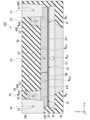
- 3 is a cross-sectional view of the vicinity of a domain wall motion element of the magnetic array according to the first embodiment.
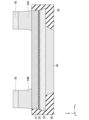
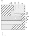
- FIG. 1 is a cross-sectional view of a domain wall motion element according to a first embodiment.
- FIG. 2 is a plan view of the domain wall motion element according to the first embodiment.
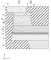
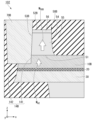
- 3 is an enlarged view of the vicinity of a first magnetization fixed layer of the domain wall motion element according to the first embodiment.
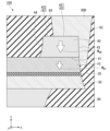
- FIG. 3 is an enlarged view of the vicinity of a second magnetization fixed layer of the domain wall motion element according to the first embodiment.
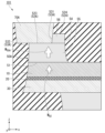
- FIG. 1 is a cross-sectional view of a domain wall motion element according to a first embodiment.
- FIG. 2 is a plan view of the domain wall motion element according to the first embodiment.
- 3 is an enlarged view of the vicinity of a first magnetization fixed
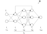
- FIG. 1 is a conceptual diagram of a neural network.
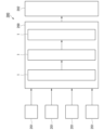
- FIG. 1 is a block diagram showing a system including a neuromorphic device according to a first embodiment.
- FIG. 1 is a block diagram showing a system including a neuromorphic device according to a first embodiment.
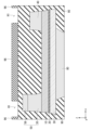
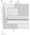
- FIG. 11 is a cross-sectional view of a domain wall motion element according to a second embodiment.
- 13 is an enlarged view of the vicinity of a first magnetization fixed layer of a domain wall motion element according to a second embodiment.
- FIG. 13 is an enlarged view of the vicinity of a second magnetization fixed layer of a domain wall motion element according to a second embodiment.
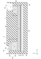
- FIG. 11 is a cross-sectional view of a domain wall motion element according to a third embodiment.
- 13 is an enlarged view of the vicinity of a first magnetization fixed layer of a domain wall motion element according to a third embodiment.
- FIG. 13 is an enlarged view of the vicinity of a second magnetization fixed layer of a domain wall motion element according to a third embodiment.
- FIG. 13 is a cross-sectional view of a domain wall motion element according to a fourth embodiment.
- 13 is an enlarged view of the vicinity of a first magnetization fixed layer of a domain wall motion element according to a fourth embodiment.
- FIG. 13 is an enlarged view of the vicinity of a second magnetization fixed layer of a domain wall motion element according to a fourth embodiment.
- FIG. 13 is a cross-sectional view of a domain wall motion element according to a fifth embodiment.
- 13 is an enlarged view of the vicinity of a first magnetization fixed layer of a domain wall motion element according to a fifth embodiment.
- FIG. 13 is an enlarged view of the vicinity of a second magnetization fixed layer of a domain wall motion element according to a fifth embodiment.
- FIG. 13 is a cross-sectional view of a domain wall motion element according to a sixth embodiment.
- FIG. 13 is a cross-sectional view of a domain wall motion element according to a seventh embodiment.
- FIG. 13 is a cross-sectional view of a domain wall motion element according to an eighth embodiment.
- the output unit 5 is connected to the resistance detection device 4.
- the output unit 5 has, for example, a processor, an output capacitor, an amplifier, a converter, etc.
- the output unit 5 may perform a calculation to substitute the detection result of the resistance detection device 4 into an activation function. The calculation is performed, for example, by a processor.
- the output unit 5 outputs the calculation result to the outside.
- the output unit 5 may perform an operation such as outputting the calculation result as an input signal for another magnetic array, or may perform an operation such as outputting the calculation result to the outside as a discrimination rate.
- the output unit 5 may also feed back the calculation result to the control device 3.
- FIG. 2 is a circuit diagram of the integrated region 1 according to the first embodiment.
- the integrated region 1 includes a plurality of domain wall motion elements 100, a plurality of write wirings WL, a plurality of common wirings CL, a plurality of read wirings RL, a plurality of first switches SW1, and a plurality of second switches SW2.
- the third switch SW3 may belong to, for example, the control device 3 in the peripheral region 2.
- the multiple domain wall motion elements 100 are arranged, for example, in a matrix.
- the multiple domain wall motion elements 100 are not limited to elements arranged in a matrix in the actual device, but may be arranged in a matrix in a circuit diagram.
- the first switch SW1, the second switch SW2, and the third switch SW3 are elements that control the flow of current.
- the first switch SW1, the second switch SW2, and the third switch SW3 are, for example, elements that utilize a phase change in a crystal layer such as a transistor or an Ovonic Threshold Switch (OTS), elements that utilize a change in band structure such as a Metal-Insulator Transition (MIT) switch, elements that utilize a breakdown voltage such as a Zener diode or an avalanche diode, and elements whose conductivity changes with a change in atomic position.
- OTS Ovonic Threshold Switch
- MIT Metal-Insulator Transition
- the positional relationship between the first switch SW1, the second switch SW2, and the third switch SW3 is not limited to that shown in FIG. 2.
- the first switch SW1 may be connected across multiple domain wall motion elements 100 and located upstream of the write wiring WL.
- the second switch SW2 may be connected across multiple domain wall motion elements 100 and located upstream of the common wiring CL.
- the third switch SW3 may be connected to each domain wall motion element 100 one by one.
- FIG. 3 is a cross-sectional view of the vicinity of the domain wall motion element 100 in the accumulation region 1 according to the first embodiment.
- FIG. 3 is a cross-section of one domain wall motion element 100 in FIG. 2 cut along the xz plane passing through the center of the width of the first ferromagnetic layer 10 in the y direction.
- the insulating layer 90 is an insulating layer that insulates between wirings of a multilayer wiring and between elements.
- the domain wall motion element 100 and the transistor Tr are electrically isolated by the insulating layer 90, except for the via wiring Vw.
- the insulating layer 90 is, for example, silicon oxide (SiO x ), silicon nitride (SiN x ), silicon carbide (SiC), chromium nitride, silicon carbonitride (SiCN), silicon oxynitride (SiON), aluminum oxide (Al 2 O 3 ), zirconium oxide (ZrO x ), or the like.
- FIG. 4 is a cross-sectional view of the domain wall motion element 100 cut in the xz plane passing through the center of the first ferromagnetic layer 10 in the y direction.
- the arrows in the figure are an example of the orientation direction of the magnetization of a ferromagnetic material.
- FIG. 5 is a plan view of the domain wall motion element 100 as seen from the z direction.
- the domain wall motion element 100 includes, for example, a first ferromagnetic layer 10, a non-magnetic layer 20, a second ferromagnetic layer 30, a first magnetization fixed layer 40, a second magnetization fixed layer 50, a first electrode 60, a second electrode 70, and a third electrode 80. At least one of the multiple domain wall motion elements included in the accumulation region 1 is the domain wall motion element 100 shown in Figures 4 and 5.
- the first ferromagnetic layer 10 extends in the x direction. When viewed from the z direction, the length of the first ferromagnetic layer 10 in the x direction is longer than the length in the y direction.
- the first ferromagnetic layer 10 has two magnetic domains inside, and a domain wall DW at the boundary between the two magnetic domains.
- the first ferromagnetic layer 10 is, for example, a layer capable of magnetically recording information by changing the magnetic state.
- the first ferromagnetic layer 10 is also called an analog layer, a magnetic recording layer, or a domain wall displacement layer.
- the first ferromagnetic layer 10 has a first magnetization region A1, a second magnetization region A2, and a third magnetization region A3.
- the first magnetization region A1 is a region in which the orientation direction of the magnetization M A1 is fixed in one direction.
- the magnetization being fixed means that the magnetization does not reverse during normal operation of the domain wall motion element 100 (when no external force exceeding the expected value is applied).
- the first magnetization region A1 is, for example, a region of the first ferromagnetic layer 10 that overlaps with the first magnetization fixed layer 40 when viewed from the z direction.
- the magnetization M A1 of the first magnetization region A1 is fixed by, for example, the magnetization M 40 of the first magnetization fixed layer 40.
- the second magnetization region A2 is a region in which the orientation direction of the magnetization M A2 is fixed in one direction.
- the orientation direction of the magnetization M A2 of the second magnetization region A2 is different from the orientation direction of the magnetization M A1 of the first magnetization region A1.
- the orientation direction of the magnetization M A2 of the second magnetization region A2 is, for example, opposite to the orientation direction of the magnetization M A1 of the first magnetization region A1.
- the second magnetization region A2 is, for example, a region of the first ferromagnetic layer 10 that overlaps with the second magnetization fixed layer 50 when viewed from the z direction.
- the magnetization M A2 of the second magnetization region A2 is, for example, fixed by the magnetization M 50 of the second magnetization fixed layer 50.
- the third magnetization region A3 is a region other than the first magnetization region A1 and the second magnetization region A2 of the first ferromagnetic layer 10.
- the third magnetization region A3 is, for example, a region sandwiched between the first magnetization region A1 and the second magnetization region A2 in the x direction.
- the third magnetized region A3 is a region where the magnetization direction changes and the domain wall DW can move.
- the third magnetized region A3 is called a domain wall movable region.
- the third magnetized region A3 has a first magnetic domain A31 and a second magnetic domain A32.
- the first magnetic domain A31 and the second magnetic domain A32 have magnetization orientation directions opposite to each other.
- the boundary between the first magnetic domain A31 and the second magnetic domain A32 is the domain wall DW.
- the magnetization M A31 of the first magnetic domain A31 is oriented in the same direction as the magnetization M A1 of the first magnetized region A1, for example.
- the magnetization M A32 of the second magnetic domain A32 is oriented in the same direction as the magnetization M A2 of the adjacent second magnetized region A2, for example.
- the domain wall DW moves within the third magnetized region A3 and does not invade the first magnetized region A1 and the second magnetized region A2.
- the domain wall DW moves.
- the domain wall DW moves by applying a write current in the x direction of the third magnetized region A3.
- a write current e.g., a current pulse
- electrons flow in the -x direction opposite to the current, and the domain wall DW moves in the -x direction.
- a current flows from the first magnetic domain A31 to the second magnetic domain A32
- the electrons spin-polarized in the second magnetic domain A32 reverse the magnetization M A31 of the first magnetic domain A31.
- the domain wall DW moves in the +x direction.
- the first ferromagnetic layer 10 is composed of a magnetic material.
- the first ferromagnetic layer 10 may be a ferromagnetic material, a ferrimagnetic material, or a combination of these with an antiferromagnetic material whose magnetic state can be changed by a current.
- the first ferromagnetic layer 10 preferably contains at least one element selected from the group consisting of Co, Ni, Fe, Pt, Pd, Gd, Tb, Mn, Ge, and Ga.
- Examples of materials used for the first ferromagnetic layer 10 include a laminated film of Co and Ni, a laminated film of Co and Pt, a laminated film of Co and Pd, a laminated film of Co x Fe 1-x B (0 ⁇ x ⁇ 1) and a material similar to the non-magnetic layer 20 described later, MnGa-based materials, GdCo-based materials, and TbCo-based materials.
- Ferrimagnetic materials such as MnGa-based materials, GdCo-based materials, and TbCo-based materials have small saturation magnetization, and the threshold current required to move the domain wall DW is small.
- the laminated film of Co and Ni, the laminated film of Co and Pt, and the laminated film of Co and Pd have large coercive force, and the moving speed of the domain wall DW is slow.
- antiferromagnetic materials include Mn 3 X (X is Sn, Ge, Ga, Pt, Ir, etc.), CuMnAs, and Mn 2 Au.
- the first ferromagnetic layer 10 may be made of the same material as the second ferromagnetic layer 30 described later. A laminate of two or more types of films or materials may also be used.
- the nonmagnetic layer 20 is sandwiched between the first ferromagnetic layer 10 and the second ferromagnetic layer 30.
- the nonmagnetic layer 20 inhibits magnetic coupling between the first ferromagnetic layer 10 and the second ferromagnetic layer 30.
- the nonmagnetic layer 20 is stacked on one side of the second ferromagnetic layer 30.
- the nonmagnetic layer 20 is a tunnel barrier layer.
- the nonmagnetic metal is, for example, Cu, Au, Ag, or the like.
- the nonmagnetic semiconductor is, for example, Si, Ge, CuInSe 2 , CuGaSe 2 , Cu(In,Ga)Se 2 , or the like.
- the second ferromagnetic layer 30 includes a ferromagnetic material.
- the second ferromagnetic layer 30 includes, for example, a material that is easy to obtain a coherent tunnel effect between the first ferromagnetic layer 10 and the second ferromagnetic layer 30.
- the second ferromagnetic layer 30 includes, for example, a metal selected from the group consisting of Cr, Mn, Co, Fe, and Ni, an alloy containing one or more of these metals, an alloy containing one or more of these metals and at least one of the elements B, C, and N, etc.
- the second ferromagnetic layer 30 is, for example, Co-Fe, Co-Fe-B, or Ni-Fe.
- a laminated film of Co and Ni, a laminated film of Co and Pt, or a laminated film of Co and Pd may be used as part of the second ferromagnetic layer 30.
- the second ferromagnetic layer 30 may be, for example, a Heusler alloy.
- the Heusler alloy is a half metal and has a high spin polarization.
- the Heusler alloy is an intermetallic compound having a chemical composition of XYZ or X 2 YZ, where X is a transition metal element or a noble metal element of the Co, Fe, Ni, or Cu group on the periodic table, Y is a transition metal element or an element type of X of the Mn, V, Cr, or Ti group, and Z is a typical element of the III group to the V group.
- Examples of Heusler alloys include Co 2 FeSi, Co 2 FeGe, Co 2 FeGa, Co 2 MnSi, Co 2 Mn 1-a Fe a Al b Si 1-b , and Co 2 FeGe 1-c Ga c .
- the second ferromagnetic layer 30 may have multiple layers and may be a synthetic antiferromagnetic structure (SAF structure).
- the synthetic antiferromagnetic structure is made up of two magnetic layers sandwiching a nonmagnetic spacer layer.
- the magnetic layers include, for example, a ferromagnetic material, and may include an antiferromagnetic material such as IrMn or PtMn.
- the spacer layer includes, for example, at least one selected from the group consisting of Ru, Ir, and Rh.
- Each of the second ferromagnetic layer 30 and the non-magnetic layer 20 is, for example, longer in the x direction than the third magnetization region A3.
- the portion where the second ferromagnetic layer 30 and the third magnetization region A3 face each other with the non-magnetic layer 20 in between is responsible for the resistance change of the domain wall motion element 100. If the length in the x direction of the second ferromagnetic layer 30 and the non-magnetic layer 20 is longer than the length in the x direction of the third region, it becomes easier to divide the resistance change width of the domain wall motion element 100 into multiple values.
- the second ferromagnetic layer 30 is, for example, longer than the first ferromagnetic layer 10 in the x direction.
- the heat dissipation of the first ferromagnetic layer 10 is improved.
- the stability of the magnetization of the first magnetization region A1 and the magnetization of the second magnetization region A2 is increased, and the reliability of the data of the domain wall motion element 100 is improved.
- the first magnetization fixed layer 40 is connected to the first ferromagnetic layer 10.
- the first magnetization fixed layer 40 is an example of a first magnetization fixed portion.
- the first magnetization fixed layer 40 is connected to the first magnetization region A1 of the first ferromagnetic layer 10.
- the magnetization M40 of the first magnetization fixed layer 40 fixes the magnetization of the first magnetization region A1.
- the second magnetization pinned layer 50 may also have a first layer 55 and a second layer 56. That is, the second magnetization pinned layer 50 may have a two-layer structure.
- the first layer 55 is closer to the first ferromagnetic layer 10 than the second layer 56.
- the first layer 55 and the second layer 56 are made of different materials.
- the first layer 55 includes, for example, the same material as the first magnetization pinned layer 40.
- the second layer 56 is a remaining portion of a mask layer 95 described later.
- the second layer 56 is, for example, Al, Cu, Ta, Ti, Zr, NiCr, a nitride (for example, TiN, TaN, SiN), or an oxide (for example, SiO 2 ).
- the second surface 42 has a connection surface 421 that contacts the first electrode 60 and a non-connection surface 422 that does not contact the first electrode 60. In other words, at least a portion of the second surface 42 does not contact the first electrode 60.
- the first side surface 43 may be located, for example, inside the domain wall motion element 100 relative to the first side surface 63 of the first electrode 60. In other words, the first side surface 43 may be located closer to the imaginary plane P3 than the first side surface 63.
- the first side surface 63 is the side surface of the first electrode 60 located on the outside of the domain wall motion element 100
- the second side surface 64 is the side surface of the first electrode 60 located on the second magnetization fixed layer 50 side.
- the second side surface 44 is, for example, located inside the domain wall motion element 100 relative to the second side surface 64 of the first electrode 60. In other words, the second side surface 44 may be located closer to the virtual plane P3 than the second side surface 64. In this case, the first electrode 60 does not overlap with the third magnetization region A3 of the first ferromagnetic layer 10 in the z direction.
- FIG. 7 is an enlarged view of the vicinity of the second magnetization fixed layer 50 of the domain wall motion element 100 according to the first embodiment.
- the second magnetization fixed layer 50 has a first surface 51, a second surface 52, a first side surface 53, and a second side surface 54.
- the first surface 51 is the surface on the first ferromagnetic layer 10 side and is in direct or indirect contact with the first ferromagnetic layer 10.
- the second surface 52 is the surface facing the first surface 51.
- the first side surface 53 is the side surface located on the outside of the domain wall motion element 100.
- the second side surface 54 is the side surface located on the first magnetization fixed layer 40 side.
- the second surface 52 has a connection surface 521 that contacts the second electrode 70 and a non-connection surface 522 that does not contact the second electrode 70. In other words, at least a portion of the second surface 52 does not contact the second electrode 70.
- the first side surface 53 may be located, for example, inside the domain wall motion element 100 relative to the first side surface 73 of the second electrode 70. In other words, the first side surface 53 may be located closer to the imaginary plane P3 than the first side surface 73.
- the first side surface 73 is the side surface of the second electrode 70 located on the outside of the domain wall motion element 100
- the second side surface 74 is the side surface of the second electrode 70 located on the first magnetization fixed layer 40 side.
- the domain wall motion element 100 may have layers other than those described above.
- a magnetic layer may be provided on the surface of the second ferromagnetic layer 30 opposite the nonmagnetic layer 20, via a spacer layer.
- the second ferromagnetic layer 30, the spacer layer, and the magnetic layer form a synthetic antiferromagnetic structure (SAF structure).
- a base layer may be provided on the surface of the magnetic layer opposite the spacer layer.
- the magnetization direction of each layer of the domain wall motion element 100 can be confirmed, for example, by measuring the magnetization curve.
- the magnetization curve can be measured, for example, using MOKE (Magneto Optical Kerr Effect). Measurement using MOKE is a measurement method in which linearly polarized light is incident on the object being measured, and the magneto-optical effect (magnetic Kerr effect) is used to cause the polarization direction to rotate, etc.
- MOKE Magnetic Magnetic Kerr Effect
- the domain wall motion element 100 is formed by a lamination process of each layer and a processing process of processing a part of each layer into a predetermined shape.
- Figures 8 to 12 are cross-sectional views for explaining the manufacturing method of the domain wall motion element 100 according to the first embodiment.
- a ferromagnetic layer 91, a nonmagnetic layer 92, a ferromagnetic layer 93, and a ferromagnetic layer 94 are laminated in this order on an insulating layer 90 including a third electrode 80.
- the layers can be laminated by sputtering, chemical vapor deposition (CVD), electron beam deposition (EB deposition), atomic laser deposition, or the like.
- the laminated body is processed to match the outer shapes of the first ferromagnetic layer 10, the nonmagnetic layer 20, and the second ferromagnetic layer 30.
- the laminated body can be processed by photolithography, etching (e.g., Ar etching), or the like.
- the ferromagnetic layer 91 becomes the second ferromagnetic layer 30, the nonmagnetic layer 92 becomes the nonmagnetic layer 20, the ferromagnetic layer 93 becomes the first ferromagnetic layer 10, and the ferromagnetic layer 94 becomes the ferromagnetic layer 94A.
- a mask layer 95 is formed at a predetermined position of the ferromagnetic layer 94A.
- the mask layer 95 is, for example, Al, Cu, Ta, Ti, Zr, NiCr, a nitride (e.g., TiN, TaN, SiN), or an oxide (e.g., SiO 2 ).
- the ferromagnetic layer 94A is processed using the mask layer 95 as a mask.
- the ferromagnetic layer 94A becomes two separated ferromagnetic layers 94B and 94C.
- the mask layer 95 on the ferromagnetic layer 94C is etched until the ferromagnetic layer 94C is exposed. At this time, a part of the ferromagnetic layer 94C may also be etched.
- the etched ferromagnetic layer 94C becomes the first magnetization fixed layer 40.
- the ferromagnetic layer 94B and the mask layer 95 each become the second magnetization fixed layer 50 consisting of a first layer 55 and a second layer 56.
- an insulating layer 90 is formed so as to fill the first magnetization fixed layer 40 and the second magnetization fixed layer 50.
- a resist 96 having openings H1 and H2 formed therein is formed on the insulating layer 90.
- the first electrode 60 and the second electrode 70 are fabricated.
- the first electrode 60 and the second electrode 70 are obtained by filling the openings H3 and H4 with a conductor, as shown in FIG. 12.
- openings H3 and H4 are formed in the insulating layer 90 using openings H1 and H2 in the resist 96. Opening H3 is formed so as to satisfy a first condition and a second condition.
- the first condition is that the center of the first electrode 60 is positioned outside the center of the first magnetization fixed layer 40 in the x direction.
- the second condition is that at least a portion of the second surface 42 of the first magnetization fixed layer 40 is not in contact with the first electrode 60.
- opening H3 is formed so that its center C1' in the x direction is located farther from the center C3 in the x direction of the first ferromagnetic layer 10 than the center C2 in the x direction of the first magnetization fixed layer 40.
- Opening H4 is formed so that its center C4' in the x direction is located farther from the center C3 in the x direction of the first ferromagnetic layer 10 than the center C4 in the x direction of the second magnetization fixed layer 50.
- the overlapping portion of the third magnetization region A3 of the first ferromagnetic layer 10 and the opening H3 in the z direction can be made smaller.
- the thickness h of the insulating layer 90 between the opening H3 and the first ferromagnetic layer 10 is thinner than the thickness of the insulating layer 90 in other portions.
- the energy used to process the opening H3 is applied to the insulating layer 90 of this thickness h.
- the thickness h When the thickness h is thin, part of the energy is applied to the first ferromagnetic layer 10, disturbing the magnetization stability of the first ferromagnetic layer 10.
- part of the opening H3 may reach the first ferromagnetic layer 10.
- the first electrode 60 and the first ferromagnetic layer 10 are short-circuited. Even if the first electrode 60 and the first ferromagnetic layer 10 are short-circuited, the domain wall DW still operates. However, the current components that do not pass through the first magnetization fixed layer 40 cannot move the domain wall DW, and the operating efficiency of the domain wall motion element 100 decreases. If the center C1' is positioned outside the center C2, the position where the opening H3 is formed is shifted, and the portion where the thickness of the insulating layer 90 is thin can be reduced.
- the center C4' is located outside the center C5, the overlapping portion of the third region of the first ferromagnetic layer 10 and the opening H4 in the z direction can be reduced.
- the energy when processing the opening H4 is applied to the insulating layer 90 with a thickness h' between the opening H4 and the first ferromagnetic layer 10.
- the thickness h' is thin, part of the energy is applied to the first ferromagnetic layer 10, disturbing the magnetization stability of the first ferromagnetic layer 10.
- part of the opening H4 may reach the first ferromagnetic layer 10.
- the opening H4 reaches the first ferromagnetic layer 10
- the second electrode 70 and the first ferromagnetic layer 10 are short-circuited, and the operating efficiency of the domain wall DW decreases.
- the center C4' is located outside the center C5
- the position where the opening H4 is formed is shifted, and the part where the insulating layer 90 is thin can be reduced.
- openings H3 and H4 are filled with a conductor.
- the conductor filled in opening H3 becomes the first electrode 60
- the conductor filled in opening H4 becomes the second electrode 70.
- the first electrode 60 satisfies the first and second conditions.
- the write operation is performed, for example, by a processor executing an operation program stored in the control unit 6.
- the control device 3 selects the domain wall motion element 100 to which a pulse is applied in accordance with the operating program.
- the domain wall motion element 100 to which the pulse is applied is an element that stores data.
- the domain wall motion element 100 to which the pulse is applied is an element that changes the weight in response to learning.
- the domain wall motion element 104 has a first ferromagnetic layer 10, a non-magnetic layer 20, a second ferromagnetic layer 30, a first magnetization fixed layer 40, a second magnetization fixed layer 50, a first electrode 60D, and a second electrode 70D.
- the first electrode 60D and the second electrode 70D differ from the first electrode 60 and the second electrode 70 in that they have different shapes or connections to other layers, but are otherwise similar in configuration.
- FIG. 26 is an enlarged view of the vicinity of the second magnetization fixed layer 50 of the domain wall motion element 104 according to the fifth embodiment.
- At least a portion of the second surface 52 of the second magnetization fixed layer 50 is not in contact with the second electrode 70D.
- the second electrode 70D is in contact with the second surface 52 and the first side surface 53 of the second magnetization fixed layer 50.
- the second electrode 70D also is in contact with the side surface of the first ferromagnetic layer 10.
- the second electrode 70D has a portion located in the -z direction from the second surface 52 of the second magnetization fixed layer 50.
- the domain wall motion element 104 according to the fifth embodiment like the domain wall motion element 100 according to the first embodiment, has a low risk of causing processing damage to the first ferromagnetic layer 10 during manufacturing. Furthermore, by satisfying this configuration, it is possible to reduce the magnetic field generated by the write current from interfering with the operation of the domain wall DW.
- Sixth Embodiment 27 is a plan view of a domain wall motion element 105 according to the sixth embodiment.
- the domain wall motion element 105 can be substituted for the domain wall motion element 100.
- the same components as those in the domain wall motion element 100 are denoted by the same reference numerals and will not be described.
- the domain wall motion element 105 has a first ferromagnetic layer 10, a non-magnetic layer 20, a second ferromagnetic layer 30, a first magnetization fixed layer 40, a second magnetization fixed layer 50, a first electrode 60E, and a second electrode 70E.
- the first electrode 60E and the second electrode 70E differ from the first electrode 60 and the second electrode 70 in that they are positioned differently in the y direction, but otherwise have the same configuration.
- both the first electrode 60E and the second electrode 70E are shifted in the +y direction relative to the first ferromagnetic layer 10, but both the first electrode 60E and the second electrode 70E may be shifted in the -y direction relative to the first ferromagnetic layer 10, or the first electrode 60E and the second electrode 70E may be shifted in different directions relative to the first ferromagnetic layer 10.
- Fig. 28 is a cross-sectional view of the domain wall motion element 106 according to the seventh embodiment.
- Fig. 28 is a cross-sectional view of the domain wall motion element 106 cut in an xz plane passing through the center of the first ferromagnetic layer 10 in the y direction.
- the domain wall motion element 106 can be replaced with the domain wall motion element 100.
- the same components as those in the domain wall motion element 100 are denoted by the same reference numerals and will not be described.
- the intermediate layer 85 is between the first magnetization fixed layer 40 and the first electrode 60F.
- the first electrode 60F is in contact with the first magnetization fixed layer 40 via the intermediate layer 85.
- the intermediate layer 85 is made of a conductive material, for example a metal.
- Fig. 29 is a cross-sectional view of the domain wall motion element 107 according to the eighth embodiment.
- Fig. 29 is a cross-sectional view of the domain wall motion element 107 cut in an xz plane passing through the center of the first ferromagnetic layer 10 in the y direction.
- the domain wall motion element 107 can be replaced with the domain wall motion element 100.
- the same components as those in the domain wall motion element 100 are denoted by the same reference numerals and will not be described.
- the domain wall motion element 107 has a first ferromagnetic layer 10, a non-magnetic layer 20, a second ferromagnetic layer 30, a first magnetization fixed layer 40, a second magnetization fixed layer 50, a first electrode 60, and a second electrode 70G.
- the second electrode 70G differs from the second electrode 70 in terms of its shape or the state of connection with other layers, but is otherwise similar in configuration.
- the central axes of the first electrode 60 and the first magnetization fixed layer 40 are misaligned, and the central axes of the second electrode 70 and the second magnetization fixed layer 50 are misaligned, but a configuration in which only one of the central axes is misaligned is also possible.
- the domain wall motion element 105 is an example in which the central axes of the first electrode 60 and the first magnetization fixed layer 40 in the x direction are misaligned, and the central axes of the second electrode 70G and the second magnetization fixed layer 50 in the x direction are aligned.
- the second magnetization fixed layer 50 is in contact with the second electrode 70E over the entire surface.
- FIG. 29 shows an example in which the x-direction central axes of the first electrode 60 and the first magnetization fixed layer 40 are misaligned and the x-direction central axes of the second electrode 70G and the second magnetization fixed layer 50 are aligned, but the x-direction central axes of the first electrode 60 and the first magnetization fixed layer 40 may be aligned and the x-direction central axes of the second electrode 70G and the second magnetization fixed layer 50 may be misaligned. Since the first magnetization fixed layer 40 is thinner than the second magnetization fixed layer 50, it is preferable that the x-direction central axes of the first electrode 60 and the first magnetization fixed layer 40 are misaligned. As shown in FIG.
- the thickness h of the insulating layer 90 between the opening H3 and the first ferromagnetic layer 10 is thinner than the thickness h' of the insulating layer 90 between the opening H4 and the first ferromagnetic layer 10. Therefore, misalignment of the central axes of the first electrode 60 and the first magnetization fixed layer 40 in the x direction reduces the risk of causing processing damage to the first ferromagnetic layer 10 when forming the opening H3.
- the central axes of the first electrode 60 and the first magnetization fixed layer 40 are misaligned, so there is little risk of processing damage to the first ferromagnetic layer 10 during manufacturing.
- This configuration also reduces the magnetic field generated by the write current interfering with the operation of the domain wall DW. Therefore, the domain wall motion element 107 according to the eighth embodiment can achieve the same effects as the domain wall motion element 100 according to the first embodiment.
- the present invention is not limited to this embodiment.
- the characteristic configurations of the embodiments may be combined, or some parts may be modified without changing the gist of the invention.
- a combination of configurations of embodiments in which the structure near the first magnetization fixed portion and the structure near the second magnetization fixed portion are different may be used.
Landscapes
- Hall/Mr Elements (AREA)
- Mram Or Spin Memory Techniques (AREA)
Abstract
この磁壁移動素子は、内部に磁壁を有する第1強磁性層と、第2強磁性層と、前記第1強磁性層と前記第2強磁性層に挟まれる非磁性層と、前記第1強磁性層に接続された第1磁化固定部と、前記第1磁化固定部と第1方向に離間した位置で、前記第1強磁性層に接続された第2磁化固定部と、前記第1磁化固定部に接続された第1電極と、前記第2磁化固定部に接続された第2電極と、を備える。前記第2強磁性層は、前記第1強磁性層より基板の近くにある。前記第1磁化固定部から前記第2磁化固定部に向かう第1方向において、前記第1電極の中心は、前記第1磁化固定部の中心より前記第1強磁性層の中心から離れた位置にある。前記第1磁化固定部は、前記第1強磁性層と接する第1面と、前記第1面と対向する第2面を有する。前記第2面の少なくとも一部は、前記第1電極と接していない。
Description
本開示は、磁壁移動素子、磁気アレイ及びニューロモルフィックデバイス及び磁壁移動素子の製造方法に関する。
二つの強磁性層の磁化の相対角の変化に基づく抵抗値変化(磁気抵抗変化)を利用した磁気抵抗効果素子が知られている。例えば、特許文献1に記載の磁壁移動型の磁気抵抗効果素子(以下、磁壁移動素子という)は、磁気抵抗効果素子の一例である。磁壁移動素子は、磁壁の位置によって積層方向の抵抗値が変化し、多値又はアナログにデータを記録できる。磁壁移動素子は、抵抗変化の線形性及び対称性が高く、書き換え耐性に優れ、高速動作が可能である。
特許文献1は、磁壁の移動範囲を制限する磁化固定部を第1磁化自由層(磁壁移動層)の両端に設けることを記載している。2つの磁化固定部は、それぞれ磁化の配向方向が異なる。
磁壁移動素子は、書き込み電流を印加することで、信号の書き込みを行う。書き込み電流は、磁化固定部に接続された電極を介して、磁壁移動素子に印加される。磁化固定部と電極との接触面積を広くするために、磁化固定部と重なる位置に電極を形成する場合が多い。しかしながら、磁化固定部の中心位置と電極の中心位置が重なる場合に、磁壁移動素子の信頼性が低下する場合がある。
本開示は上記問題に鑑みてなされたものであり、信頼性の高い、磁壁移動素子、磁気アレイ及びニューロモルフィックデバイスを提供することを目的とする。
第1の態様に係る磁壁移動素子は、内部に磁壁を有する第1強磁性層と、第2強磁性層と、前記第1強磁性層と前記第2強磁性層に挟まれる非磁性層と、前記第1強磁性層に接続された第1磁化固定部と、前記第1磁化固定部と第1方向に離間した位置で、前記第1強磁性層に接続された第2磁化固定部と、前記第1磁化固定部に接続された第1電極と、前記第2磁化固定部に接続された第2電極と、を備える。前記第2強磁性層は、前記第1強磁性層より基板の近くにある。前記第1磁化固定部から前記第2磁化固定部に向かう第1方向において、前記第1電極の中心は、前記第1磁化固定部の中心より前記第1強磁性層の中心から離れた位置にある。前記第1磁化固定部は、前記第1強磁性層と接する第1面と、前記第1面と対向する第2面を有する。前記第2面の少なくとも一部は、前記第1電極と接していない。
以下、本実施形態について、図を適宜参照しながら詳細に説明する。以下の説明で用いる図面は、本実施形態の特徴をわかりやすくするために便宜上特徴となる部分を拡大して示している場合があり、各構成要素の寸法比率などは実際とは異なっていることがある。以下の説明において例示される材料、寸法等は一例であって、本実施形態はそれらに限定されるものではなく、本実施形態の効果を奏する範囲で適宜変更して実施することが可能である。
まず方向について定義する。x方向及びy方向は、後述する基板Sub(図3参照)の一面と略平行な方向である。x方向は、後述する第1強磁性層が延びる方向である。x方向は、第1方向の一例である。以下の図では、-x方向を第1方向とする。y方向は、x方向と直交する方向である。y方向は、第2方向の一例である。z方向は、後述する基板から磁壁移動素子へ向かう方向である。z方向は、積層方向の一例である。本明細書において、+z方向を「上」、-z方向を「下」として表す場合があるが、これら表現は便宜上のものであり、重力方向を規定するものではない。また本明細書で「x方向に延びる」とは、例えば、x方向、y方向、及びz方向の各寸法のうち最小の寸法よりもx方向の寸法が大きいことを意味する。他の方向に延びる場合も同様である。
[第1実施形態]
図1は、第1実施形態にかかる磁気アレイMAのブロック図である。磁気アレイMAは、集積領域1と周辺領域2とを有する。磁気アレイMAは、例えば、磁気メモリ、積和演算器、ニューロモーフィックデバイス、スピンメモリスタ、磁気光学素子に利用できる。
図1は、第1実施形態にかかる磁気アレイMAのブロック図である。磁気アレイMAは、集積領域1と周辺領域2とを有する。磁気アレイMAは、例えば、磁気メモリ、積和演算器、ニューロモーフィックデバイス、スピンメモリスタ、磁気光学素子に利用できる。
集積領域1は、複数の磁壁移動素子が集積された領域である。磁気アレイMAをメモリとして用いる場合は、集積領域1にデータが蓄積される。磁気アレイMAをニューロモーフィックデバイスとして用いる場合は、集積領域1で学習及び推論が行われる。
周辺領域2は、集積領域1内の磁壁移動素子の動作を制御する制御素子が実装されている領域である。周辺領域2は、例えば、制御装置3、抵抗検出装置4、出力部5を有する。
制御装置3は、集積領域1内の複数の磁壁移動素子の少なくとも一つにパルスを印加できるように構成されている。制御装置3は、例えば、制御部6と電源7とを有する。
制御部6は、例えば、プロセッサとメモリとを有する。プロセッサは、例えば、CPU(Central Processing Unit)である。プロセッサは、メモリに記憶された動作プログラムに基づいて動作する。制御部6は、例えば、パルスを印加する磁壁移動素子のアドレス、所定の磁壁移動素子に印加するパルスの大きさ(電圧、パルス長)等を制御する。制御部6は、この他、クロック、カウンタ、乱数発生器等を有してもよい。クロックは、パルスを印加するタイミングの指標となり、カウンタは、パルスを印加した回数等をカウントする。電源7は、制御部6からの指示に従い、磁壁移動素子に向かってパルスを印加する。
抵抗検出装置4は、集積領域1内の磁壁移動素子の抵抗値を検出できるように構成されている。抵抗検出装置4は、集積領域1内の磁壁移動素子のそれぞれの抵抗を検出してもよいし、例えば同じ列に属する磁壁移動素子の抵抗の合計を検出してもよい。抵抗検出装置4は、例えは、検出した抵抗値の大きさを比較する比較器を有する。比較器は、例えば、検出した抵抗値同士を比較してもよいし、事前に設定された基準抵抗値と検出した抵抗値とを比較してもよい。
出力部5は、抵抗検出装置4に接続されている。出力部5は、例えば、プロセッサ、出力コンデンサ、増幅器、コンバータ等を有する。磁気アレイMAをニューロモーフィックデバイスとして用いる場合は、出力部5は、抵抗検出装置4の検出結果を活性化関数に代入する演算を行ってもよい。演算は、例えば、プロセッサで行われる。出力部5は、演算結果を外部に出力する。磁気アレイMAをニューロモーフィックデバイスとして用いる場合は、例えば、演算結果を他の磁気アレイの入力信号として出力する等の動作を行ってもよいし、識別率として外部に出力する等の動作を行ってもよい。また出力部5は、演算結果を制御装置3にフィードバックしてもよい。
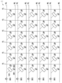
図2は、第1実施形態に係る集積領域1の回路図である。集積領域1は、複数の磁壁移動素子100と、複数の書き込み配線WLと、複数の共通配線CLと、複数の読出し配線RLと、複数の第1スイッチSW1と、複数の第2スイッチSW2と、を備える。第3スイッチSW3は、例えば、周辺領域2の制御装置3に属してもよい。
複数の磁壁移動素子100は、例えば、行列状に配列する。複数の磁壁移動素子100は、実物の素子が行列状に配列するものに限られず、回路図において行列に配列するものでもよい。
書き込み配線WLのそれぞれは、データの書き込み時に用いられる。書き込み配線WLはそれぞれ、制御装置3と1つ以上の磁壁移動素子100とを電気的に接続する。共通配線CLのそれぞれは、データの書き込み時及び読み出し時の両方に用いる。共通配線CLのそれぞれは、例えば、抵抗検出装置4に接続されている。共通配線CLは、複数の磁壁移動素子100のそれぞれに設けられてもよいし、複数の磁壁移動素子100に亘って設けられてもよい。読出し配線RLのそれぞれは、データの読出し時に用いられる。読出し配線RLはそれぞれ、制御装置3と1つ以上の磁壁移動素子100とを電気的に接続する。
第1スイッチSW1、第2スイッチSW2及び第3スイッチSW3は、電流の流れを制御する素子である。第1スイッチSW1、第2スイッチSW2及び第3スイッチSW3は、例えば、トランジスタ、オボニック閾値スイッチ(OTS:Ovonic Threshold Switch)のように結晶層の相変化を利用した素子、金属絶縁体転移(MIT)スイッチのようにバンド構造の変化を利用した素子、ツェナーダイオード及びアバランシェダイオードのように降伏電圧を利用した素子、原子位置の変化に伴い伝導性が変化する素子である。
第1スイッチSW1、第2スイッチSW2は、例えば、それぞれの磁壁移動素子100に一つずつ接続されている。第1スイッチSW1は、例えば、磁壁移動素子100と書き込み配線WLとの間に接続されている。第2スイッチSW2は、例えば、磁壁移動素子100と共通配線CLとの間に接続されている。第3スイッチSW3は、例えば、複数の磁壁移動素子100に亘って接続されている。第3スイッチSW3は、例えば、読出し配線RLに接続されている。
第1スイッチSW1、第2スイッチSW2及び第3スイッチSW3の位置関係は、図2に示す場合に限られない。例えば、第1スイッチSW1は、複数の磁壁移動素子100に亘って接続され、書き込み配線WLの上流に位置してもよい。また例えば、第2スイッチSW2は、複数の磁壁移動素子100に亘って接続され、共通配線CLの上流に位置してもよい。また例えば、第3スイッチSW3は、それぞれの磁壁移動素子100に一つずつ接続されていてもよい。
図3は、第1実施形態に係る集積領域1の磁壁移動素子100の近傍の断面図である。図3は、図2における一つの磁壁移動素子100を第1強磁性層10のy方向の幅の中心を通るxz平面で切断した断面である。
図3に示す第1スイッチSW1及び第2スイッチSW2は、トランジスタTrである。トランジスタTrは、ゲート電極Gと、ゲート絶縁膜GIと、基板Subに形成されたソースS及びドレインDと、を有する。ソースSとドレインDは、電流の流れ方向によって既定されるものであり、いずれも半導体の活性領域である。図3は一例を示しただけであり、ソースSとドレインDの位置関係は反転していてもよい。基板Subは、例えば、半導体基板である。第3スイッチSW3は、読出し配線RLと電気的に接続され、例えば、図3においてy方向にずれた位置にある。
トランジスタTr、書き込み配線WL、共通配線CL、読出し配線RL及び磁壁移動素子100の間は、z方向に延びるビア配線Vw又はxy面内のいずれかの方向に延びる面内配線IPwで接続されている。ビア配線Vw及び面内配線IPwは、導電性を有する材料を含む。z方向の異なる階層間は、ビア配線Vwを除いて、絶縁層90が形成されている。
絶縁層90は、多層配線の配線間や素子間を絶縁する絶縁層である。磁壁移動素子100とトランジスタTrとは、ビア配線Vwを除いて、絶縁層90によって電気的に分離されている。絶縁層90は、例えば、酸化シリコン(SiOx)、窒化シリコン(SiNx)、炭化シリコン(SiC)、窒化クロム、炭窒化シリコン(SiCN)、酸窒化シリコン(SiON)、酸化アルミニウム(Al2O3)、酸化ジルコニウム(ZrOx)等である。
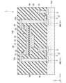
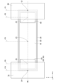
図4は、磁壁移動素子100を第1強磁性層10のy方向の中心を通るxz平面で切断した断面図である。図に示す矢印は、強磁性体の磁化の配向方向の一例である。図5は、磁壁移動素子100をz方向から見た平面図である。
磁壁移動素子100は、例えば、第1強磁性層10と非磁性層20と第2強磁性層30と第1磁化固定層40と第2磁化固定層50と第1電極60と第2電極70と第3電極80とを備える。集積領域1に含まれる複数の磁壁移動素子のうち少なくとも一つは、図4及び図5に示す磁壁移動素子100である。
第1強磁性層10は、x方向に延びる。第1強磁性層10は、z方向から見ると、x方向の長さがy方向の長さより長い。第1強磁性層10は、内部に2つの磁区を有し、2つの磁区の境界に磁壁DWを有する。第1強磁性層10は、例えば、磁気的な状態の変化により情報を磁気記録可能な層である。第1強磁性層10は、アナログ層、磁気記録層、磁壁移動層とも呼ばれる。
第1強磁性層10は、第1磁化領域A1と第2磁化領域A2と第3磁化領域A3を有する。
第1磁化領域A1は、磁化MA1の配向方向が一方向に固定された領域である。磁化が固定されているとは、磁壁移動素子100の通常の動作(想定を超える外力が印加されていない)において、磁化が反転しないことをいう。第1磁化領域A1は、例えば、第1強磁性層10のうちz方向からみて第1磁化固定層40と重なる領域である。第1磁化領域A1の磁化MA1は、例えば、第1磁化固定層40の磁化M40によって固定されている。
第2磁化領域A2は、磁化MA2の配向方向が一方向に固定された領域である。第2磁化領域A2の磁化MA2の配向方向は、第1磁化領域A1の磁化MA1の配向方向と異なる。第2磁化領域A2の磁化MA2の配向方向は、例えば、第1磁化領域A1の磁化MA1の配向方向と反対である。第2磁化領域A2は、例えば、第1強磁性層10のうちz方向からみて第2磁化固定層50と重なる領域である。第2磁化領域A2の磁化MA2は、例えば、第2磁化固定層50の磁化M50によって固定されている。
第3磁化領域A3は、第1強磁性層10の第1磁化領域A1及び第2磁化領域A2以外の領域である。第3磁化領域A3は、例えば、x方向に第1磁化領域A1と第2磁化領域A2とに挟まれる領域である。
第3磁化領域A3は、磁化の向きが変化し、磁壁DWが移動できる領域である。第3磁化領域A3は、磁壁移動可能領域と称される。第3磁化領域A3は、第1磁区A31と第2磁区A32とを有する。第1磁区A31と第2磁区A32とは、磁化の配向方向が反対である。第1磁区A31と第2磁区A32との境界が磁壁DWである。第1磁区A31の磁化MA31は、例えば、第1磁化領域A1の磁化MA1と同じ方向に配向する。第2磁区A32の磁化MA32は、例えば、隣接する第2磁化領域A2の磁化MA2と同じ方向に配向する。磁壁DWは、原則、第3磁化領域A3内を移動し、第1磁化領域A1及び第2磁化領域A2には侵入しない。
第3磁化領域A3内における第1磁区A31と第2磁区A32との体積の比率が変化すると、磁壁DWが移動する。磁壁DWは、第3磁化領域A3のx方向に書き込み電流を流すことによって移動する。例えば、第3磁化領域A3に+x方向の書き込み電流(例えば、電流パルス)を印加すると、電子は電流と逆の-x方向に流れるため、磁壁DWは-x方向に移動する。第1磁区A31から第2磁区A32に向って電流が流れる場合、第2磁区A32でスピン偏極した電子は、第1磁区A31の磁化MA31を磁化反転させる。第1磁区A31の磁化MA31が反転することで、磁壁DWは+x方向に移動する。
第1強磁性層10は、磁性体により構成される。第1強磁性層10は、強磁性体、フェリ磁性体、又はこれらと電流により磁気状態を変化させることが可能な反強磁性体との組み合わせでもよい。第1強磁性層10は、Co、Ni、Fe、Pt、Pd、Gd、Tb、Mn、Ge、Gaからなる群から選択される少なくとも一つの元素を有することが好ましい。
第1強磁性層10に用いられる材料として、例えば、CoとNiの積層膜、CoとPtの積層膜、CoとPdの積層膜、CoxFe1-xB(0≦x≦1)と後述する非磁性層20と同様の材料との積層膜、MnGa系材料、GdCo系材料、TbCo系材料が挙げられる。MnGa系材料、GdCo系材料、TbCo系材料等のフェリ磁性体は飽和磁化が小さく、磁壁DWを移動するために必要な閾値電流が小さくなる。またCoとNiの積層膜、CoとPtの積層膜、CoとPdの積層膜は、保磁力が大きく、磁壁DWの移動速度が遅くなる。反強磁性体は、例えば、Mn3X(XはSn、Ge、Ga、Pt、Ir等)、CuMnAs、Mn2Au等である。第1強磁性層10には、後述する第2強磁性層30と同様の材料を適用することもできる。2種以上の積層膜、材料を適用する事もできる。
非磁性層20は、第1強磁性層10と第2強磁性層30とに挟まれる。非磁性層20は、第1強磁性層10と第2強磁性層30との間の磁気的な結合を阻害する。非磁性層20は、第2強磁性層30の一面に積層される。
非磁性層20は、例えば、非磁性の絶縁体、半導体又は金属からなる。非磁性層20は、例えば、非磁性の絶縁体であることが好ましい。非磁性の絶縁体は、例えば、Al2O3、SiO2、MgO、MgAl2O4、およびこれらのAl、Si、Mgの一部がZn、Be、Ga、Ti等に置換された材料である。これらの材料は、バンドギャップが大きく、絶縁性に優れる。非磁性の絶縁体は、例えば、Mg又はAlを含む酸化物である。非磁性層20が非磁性の絶縁体からなる場合、非磁性層20はトンネルバリア層である。非磁性の金属は、例えば、Cu、Au、Ag等である。非磁性の半導体は、例えば、Si、Ge、CuInSe2、CuGaSe2、Cu(In,Ga)Se2等である。
非磁性層20の厚みは、例えば、20Å以上であり、25Å以上でもよい。
第2強磁性層30は、第1強磁性層10と共に、非磁性層20を挟む。第2強磁性層30は、少なくとも一部が第3磁化領域A3とz方向に重なる位置にある。第2強磁性層30は、例えば、第1強磁性層10より基板Subの近くにある。
第2強磁性層30の磁化M30は、第1強磁性層10の第3磁化領域A3の磁化より反転しにくい。第2強磁性層30の磁化M30は、第3磁化領域A3の磁化が反転する程度の外力が印加された際に向きが変化せず、固定されている。第2強磁性層30は、固定層、参照層と言われる場合もある。
第2強磁性層30は、強磁性体を含む。第2強磁性層30は、例えば、第1強磁性層10との間で、コヒーレントトンネル効果を得やすい材料を含む。第2強磁性層30は、例えば、Cr、Mn、Co、Fe及びNiからなる群から選択される金属、これらの金属を1種以上含む合金、これらの金属とB、C、及びNの少なくとも1種以上の元素とが含まれる合金等を含む。第2強磁性層30は、例えば、Co-Fe、Co-Fe-B、Ni-Feである。また、第2強磁性層30の一部に、CoとNiの積層膜、CoとPtの積層膜、CoとPdの積層膜を用いても良い。
第2強磁性層30は、例えば、ホイスラー合金でもよい。ホイスラー合金はハーフメタルであり、高いスピン分極率を有する。ホイスラー合金は、XYZ又はX2YZの化学組成をもつ金属間化合物であり、Xは周期表上でCo、Fe、Ni、あるいはCu族の遷移金属元素または貴金属元素であり、YはMn、V、CrあるいはTi族の遷移金属又はXの元素種であり、ZはIII族からV族の典型元素である。ホイスラー合金として例えば、Co2FeSi、Co2FeGe、Co2FeGa、Co2MnSi、Co2Mn1-aFeaAlbSi1-b、Co2FeGe1-cGac等が挙げられる。
第2強磁性層30は、複数の層を有し、シンセティック反強磁性構造(SAF構造)でもよい。シンセティック反強磁性構造は、非磁性のスペーサ層を挟む二つの磁性層からなる。磁性層は、例えば、強磁性体を含み、IrMn、PtMn等の反強磁性体を含んでもよい。スペーサ層は、例えば、Ru、Ir、Rhからなる群から選択される少なくとも一つを含む。
第2強磁性層30及び非磁性層20のそれぞれは、例えば、x方向において、第3磁化領域A3より長い。非磁性層20を挟んで第2強磁性層30と第3磁化領域A3とが向き合う部分が、磁壁移動素子100の抵抗変化を担う。第2強磁性層30及び非磁性層20のx方向の長さが第3領域のx方向の長さより長いと、磁壁移動素子100の抵抗変化幅をより多値に区分しやすくなる。
第2強磁性層30は、例えば、x方向において、第1強磁性層10より長い。z方向から見て第2強磁性層30が第1強磁性層10の全体と重畳すると、第1強磁性層10の放熱性が向上する。その結果、第1磁化領域A1の磁化及び第2磁化領域A2の磁化の安定性が高まり、磁壁移動素子100のデータの信頼性が高まる。
第1磁化固定層40は、第1強磁性層10に接続されている。第1磁化固定層40は、第1磁化固定部の一例である。第1磁化固定層40は、第1強磁性層10の第1磁化領域A1に接続されている。第1磁化固定層40の磁化M40は第1磁化領域A1の磁化を固定する。
第1磁化固定層40は、例えば、強磁性体である。第1磁化固定層40は、例えば、第1強磁性層10又は第2強磁性層30と同様の材料を適用できる。第1磁化固定層40は、複数の層を有してもよい。例えば、第1磁化固定層40は、複数の層の積層構造でもよく、製造時のマスク層、キャップ層等を含んでもよい。
第1磁化固定層40は、複数の層を有し、シンセティック反強磁性構造(SAF構造)でもよい。シンセティック反強磁性構造は、非磁性のスペーサ層を挟む二つの磁性層からなる。磁性層は、例えば、強磁性体を含み、IrMn、PtMn等の反強磁性体を含んでもよい。スペーサ層は、例えば、Ru、Ir、Rhからなる群から選択される少なくとも一つを含む。
また第1磁化固定層40は、強磁性体に限られない。第1磁化固定層40が強磁性体ではない場合は、第1磁化固定層40と重なる領域で第1強磁性層10を流れる電流の電流密度が急激に変化することで、磁壁DWの移動が制限され、第1磁化領域A1の磁化が固定される。
第2磁化固定層50は、第1磁化固定層40とx方向に離間した位置で、第1強磁性層10に接続されている。第2磁化固定層50は、第2磁化固定部の一例である。第2磁化固定層50は、第1強磁性層10の第2磁化領域A2に接続されている。第2磁化固定層50の磁化M50は第2磁化領域A2の磁化を固定する。
第2磁化固定層50は、第1磁化固定層40と同様の材料を用いることができる。第2磁化固定層50は、シンセティック反強磁性構造(SAF構造)でもよい。第2磁化固定層50は、複数の層を有してもよい。例えば、第2磁化固定層50は、複数の層の積層構造でもよく、製造時のマスク層、キャップ層等を含んでもよい。
第1磁化固定層40の膜厚と第2磁化固定層50の膜厚とは、同じでも、異なってもよい。例えば、第1磁化固定層40の膜厚は、第2磁化固定層50の膜厚より厚い。第1磁化固定層40の膜厚と第2磁化固定層50の膜厚とが異なると、第1磁化固定層40と第2磁化固定層50の保磁力に差が生じやすい。第1磁化固定層40と第2磁化固定層50との間に保磁力差があると、製造時点で、第1磁化固定層40の磁化M40の配向方向と第2磁化固定層50の磁化M50の配向方向とを異なる方向に設定しやすくなる。
また第2磁化固定層50は、第1層55と第2層56とを有してもよい。すなわち、第2磁化固定層50は、2層構造でもよい。第1層55は、第2層56より第1強磁性層10の近くにある。第1層55と第2層56とは、異なる材料からなる。第1層55は、例えば、第1磁化固定層40と同様の材料を含む。第2層56は、後述するマスク層95の一部が残存したものである。第2層56は、例えば、Al、Cu、Ta、Ti、Zr、NiCr、窒化物(例えばTiN、TaN、SiN)、酸化物(例えばSiO2)である。
第1層55と第2層56との境界面の位置は、任意である。例えば、第1層55と第2層56との境界面のz方向の位置は、第1磁化固定層40の上面(第2面42)のz方向の位置と同じでもよい。
ここで、第1磁化固定層40と第2磁化固定層50の位置関係は、図4に示す例に限られない。第1磁化固定層40と第2磁化固定層50の位置関係は反対でもよく、第1磁化固定層40が第2磁化固定層50の+x方向の位置にあってもよい。
第1電極60は、第1磁化固定層40に接続されている。第1電極60は、第1磁化固定層40と直接接してもよいし、層を挟んで間接的に接続してもよい。第1電極60は、例えば、磁壁移動素子100に書き込み電流を印加する際に用いられる書き込み電極である。書き込み電流は、第1電極60と第2電極70との間に流れる。第1電極60は、導電性を有する材料を含む。
第2電極70は、第2磁化固定層50に接続されている。第2電極70は、第2磁化固定層50と直接接してもよいし、層を挟んで間接的に接続してもよい。第2電極70は、磁壁移動素子100に書き込み電流を印加する際、及び、磁壁移動素子100に読出し電流を印加する際に用いられる共通電極である。第2電極70は、導電性を有する材料を含む。
第3電極80は、第2強磁性層30に接続されている。第3電極80は、第2強磁性層30と直接接してもよいし、層を挟んで間接的に接続してもよい。第3電極80は、磁壁移動素子100に読出し電流を印加する際に用いられる読み出し電極である。第3電極80は、導電性を有する材料を含む。
第1電極60のx方向の中心C1は、第1磁化固定層40のx方向の中心C2より第1強磁性層10のx方向の中心C3から離れた位置にある。中心C1、C2、C3のそれぞれを通るyz面をそれぞれ仮想面P1、P2、P3とすると、x方向において、仮想面P1は、仮想面P2より仮想面P3から離れた位置にある。
同様に、第2電極70のx方向の中心C4は、第2磁化固定層50のx方向の中心C5より第1強磁性層10のx方向の中心C3から離れた位置にある。中心C1、C4、C5のそれぞれを通るyz面をそれぞれ仮想面P1、P4、P5とすると、x方向において、仮想面P4は、仮想面P5より仮想面P3から離れた位置にある。
図5に示す例では、第1磁化固定層40、第2磁化固定層50、第1電極60、第2電極70のy方向の中心C1、C2、C4、C5は、y方向の同じ位置にあり、同一の仮想面P6上にある。
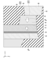
図6は、第1実施形態に係る磁壁移動素子100の第1磁化固定層40の近傍の拡大図である。第1磁化固定層40は、第1面41と第2面42と第1側面43と第2側面44とを有する。
第1面41は、第1強磁性層10側の面であり、第1強磁性層10と直接または間接的に接する面である。第2面42は、第1面41と対向する面である。第1側面43は、磁壁移動素子100の外側に位置する側面である。第2側面44は、第2磁化固定層50側に位置する側面である。
第2面42は、第1電極60と接する接続面421と、第1電極60と接しない非接続面422と、を有する。すなわち、第2面42の少なくとも一部は、第1電極60と接していない。
第1側面43は、例えば、第1電極60の第1側面63より磁壁移動素子100の内側にあってもよい。すなわち、第1側面43は、第1側面63より仮想面P3の近くにあってもよい。第1側面63は、第1電極60の磁壁移動素子100の外側に位置する側面であり、第2側面64は、第1電極60の第2磁化固定層50側に位置する側面である。
また第2側面44は、例えば、第1電極60の第2側面64より磁壁移動素子100の内側にある。すなわち、第2側面44は、第2側面64より仮想面P3の近くにあってもよい。この場合、第1電極60は、第1強磁性層10の第3磁化領域A3とz方向に重ならない。
図7は、第1実施形態に係る磁壁移動素子100の第2磁化固定層50の近傍の拡大図である。第2磁化固定層50は、第1面51と第2面52と第1側面53と第2側面54とを有する。
第1面51は、第1強磁性層10側の面であり、第1強磁性層10と直接または間接的に接する面である。第2面52は、第1面51と対向する面である。第1側面53は、磁壁移動素子100の外側に位置する側面である。第2側面54は、第1磁化固定層40側に位置する側面である。
第2面52は、第2電極70と接する接続面521と、第2電極70と接しない非接続面522と、を有する。すなわち、第2面52の少なくとも一部は、第2電極70と接していない。
第1側面53は、例えば、第2電極70の第1側面73より磁壁移動素子100の内側にあってもよい。すなわち、第1側面53は、第1側面73より仮想面P3の近くにあってもよい。第1側面73は、第2電極70の磁壁移動素子100の外側に位置する側面であり、第2側面74は、第2電極70の第1磁化固定層40側に位置する側面である。
また第2側面54は、例えば、第2電極70の第2側面74より磁壁移動素子100の内側にある。すなわち、第2側面54は、第2側面74より仮想面P3の近くにあってもよい。この場合、第2電極70は、第1強磁性層10の第3磁化領域A3とz方向に重ならない。
磁壁移動素子100は、上記の構成以外の層を有してもよい。例えば、第2強磁性層30の非磁性層20と反対側の面に、スペーサ層を介して、磁性層を設けてもよい。第2強磁性層30、スペーサ層、磁性層は、シンセティック反強磁性構造(SAF構造)となる。また、磁性層のスペーサ層と反対側の面に、下地層を設けてもよい。
磁壁移動素子100の各層の磁化の向きは、例えば磁化曲線を測定することにより確認できる。磁化曲線は、例えば、MOKE(Magneto Optical Kerr Effect)を用いて測定できる。MOKEによる測定は、直線偏光を測定対象物に入射させ、その偏光方向の回転等が起こる磁気光学効果(磁気Kerr効果)を用いることにより行う測定方法である。
磁壁移動素子100は、各層の積層工程と、各層の一部を所定の形状に加工する加工工程により形成される。図8~図12は、第1実施形態に係る磁壁移動素子100の製造方法を説明するための断面図である。
まず第1工程として、図8に示すように、第3電極80を含む絶縁層90上に、強磁性層91、非磁性層92、強磁性層93、強磁性層94を順に積層する。各層の積層は、スパッタリング法、化学気相成長(CVD)法、電子ビーム蒸着法(EB蒸着法)、原子レーザデポジッション法等を用いることができる。
次いで、図9に示すように、積層した積層体を、第1強磁性層10、非磁性層20及び第2強磁性層30の外形に合わせて加工する。積層体の加工は、フォトリソグラフィーおよびエッチング(例えば、Arエッチング)等を用いて行うことができる。強磁性層91は第2強磁性層30となり、非磁性層92は非磁性層20となり、強磁性層93は第1強磁性層10となり、強磁性層94は強磁性層94Aとなる。そして強磁性層94Aの所定の位置にマスク層95を形成する。マスク層95は、例えば、Al、Cu、Ta、Ti、Zr、NiCr、窒化物(例えばTiN、TaN、SiN)、酸化物(例えばSiO2)である。
次いで、第2工程として、図10に示すように、マスク層95をマスクとして、強磁性層94Aを加工する。強磁性層94Aは、2つの離間した強磁性層94Bと強磁性層94Cとなる。
次いで、強磁性層94Cが露出するまで、強磁性層94C上のマスク層95をエッチングする。この際、強磁性層94Cの一部もエッチングされてもよい。エッチングされた強磁性層94Cは、第1磁化固定層40となる。強磁性層94Bとマスク層95のそれぞれは、第1層55と第2層56とからなる第2磁化固定層50となる。そして、図11に示すように、第1磁化固定層40及び第2磁化固定層50を埋めるように、絶縁層90を形成する。そして、絶縁層90上に、開口H1,H2が形成されたレジスト96を形成する。
次いで、第3工程及び第4工程として第1電極60及び第2電極70を作製する。第1電極60及び第2電極70は、図12に示すように、開口H3、H4を導体で充填することで得られる。
まず図12に示すように、レジスト96の開口H1,H2を利用して、絶縁層90に開口H3,H4を形成する。開口H3は、第1条件および第2条件を満たすように形成する。第1条件は、x方向において、第1電極60の中心を第1磁化固定層40の中心より外側に配置するという条件である。また第2条件は、第1磁化固定層40の第2面42の少なくとも一部が第1電極60と接しないという条件である。
例えば、開口H3は、開口H3のx方向の中心C1’が、第1磁化固定層40のx方向の中心C2より第1強磁性層10のx方向の中心C3から離れた位置となるように形成する。開口H4は、開口H4のx方向の中心C4’が、第2磁化固定層50のx方向の中心C4より第1強磁性層10のx方向の中心C3から離れた位置となるように形成する。開口H3,H4を形成後に、レジスト96は除去される。
中心C1’が中心C2より外側に位置すると、第1強磁性層10の第3磁化領域A3と開口H3とがz方向に重なる部分を小さくできる。開口H3と第1強磁性層10とがz方向に重なる場合、開口H3と第1強磁性層10との間にある絶縁層90の厚さhは、他の部分の絶縁層90の厚さより薄い。開口H3と第1強磁性層10とがz方向に重なる場合、開口H3を加工する際のエネルギーが、この厚さhの絶縁層90に加わる。厚さhの厚みが薄い場合、そのエネルギーの一部は第1強磁性層10に加わり、第1強磁性層10の磁化安定性を乱す。また厚さhが薄い場合、開口H3の一部が第1強磁性層10に至る場合もある。開口H3が第1強磁性層10に至ると、第1電極60と第1強磁性層10とが短絡する。第1電極60と第1強磁性層10とが短絡しても、磁壁DWは動作する。しかしながら、第1磁化固定層40を通らない電流成分は、磁壁DWを動かすことができないので、磁壁移動素子100の動作効率が低下する。中心C1’が中心C2より外側に位置すると、開口H3が形成される位置がずれ、絶縁層90の厚みが薄くなる部分を減らすことができる。
同様に、中心C4’が中心C5より外側に位置すると、第1強磁性層10の第3領域と開口H4とがz方向に重なる部分を小さくできる。開口H4と第1強磁性層10とがz方向に重なる場合、開口H4と第1強磁性層10との間にある厚さh’の絶縁層90に、開口H4を加工する際のエネルギーが加わる。厚さh’の厚みが薄い場合、そのエネルギーの一部は第1強磁性層10に加わり、第1強磁性層10の磁化安定性を乱す。また厚さh’が薄い場合、開口H4の一部が第1強磁性層10に至る場合もある。開口H4が第1強磁性層10に至ると、第2電極70と第1強磁性層10とが短絡し、磁壁DWの動作効率が低下する。中心C4’が中心C5より外側に位置すると、開口H4が形成される位置がずれ、絶縁層90の厚みが薄くなる部分を減らすことができる。
次いで、開口H3及び開口H4を導電体で充填する。開口H3に充填された導電体は第1電極60となり、開口H4に充填された導電体は第2電極70となる。第1電極60は、第1条件及び第2条件を満たす。
次いで、磁気アレイMAへの信号の書き込み動作及び磁気アレイMAからの信号の読出し動作を説明する。
まず磁気アレイMAへの信号の書き込み動作について説明する。書き込み動作は、例えば、制御部6に格納された動作プログラムをプロセッサが実行することで行われる。
まず制御装置3は、動作プログラムに従い、パルスを印加する磁壁移動素子100を選択する。磁気アレイMAを磁気メモリとして用いる場合、パルスを印加する磁壁移動素子100は、データを記憶させる素子である。磁気アレイMAをニューラルネットワークとして用いる場合、パルスを印加する磁壁移動素子100は、学習に応じて重みを変化させる素子である。
複数の磁壁移動素子100のうち何れの磁壁移動素子100に対してパルスを印加するかは、制御部6が制御する。制御部6は、パルスを印加する磁壁移動素子100に接続された第1スイッチSW1及び第2スイッチSW2をONにし、第3スイッチSW3をOFFにする。またパルスを印加しない磁壁移動素子100に接続された第1スイッチSW1及び第2スイッチSW2の少なくともいずれか一方をOFFにする。
そして、制御装置3は、動作プログラムに従い、磁壁移動素子100に向かって書き込みパルスを出力する。書き込みパルスは、磁壁移動素子100の第1強磁性層10に沿って、第1磁化固定層40と第2磁化固定層50との間に印加される。書き込みパルスは、矩形波でも、スパイク波でも、その他の波形の波でもよい。書き込みパルスの回数、大きさ等を変えることで、磁壁DWの位置が変化し、特定の磁壁移動素子100に信号が書き込まれる。
次いで、磁気アレイMAからの信号の読出し動作について説明する。読出し動作は、例えば、制御部6に格納された動作プログラムをプロセッサが実行することで行われる。
まず制御装置3は、動作プログラムに従い、読出しパルスを印加する磁壁移動素子100を選択する。磁気アレイMAを磁気メモリとして用いる場合、読出しパルスを印加する磁壁移動素子100は、データを読み出す素子である。磁気アレイMAをニューラルネットワークとして用いる場合、所定の磁壁移動素子100への読出しパルスの印加は、入力と重みとの積演算に対応する。すなわち、磁気アレイMAをニューラルネットワークとして用いる場合、読出し動作は、ニューラルネットワークの識別演算である。
複数の磁壁移動素子100のうち何れの磁壁移動素子100に対してパルスを印加するかは、制御部6が制御する。制御部6は、パルスを印加する磁壁移動素子100に接続された第3スイッチSW3及び第2スイッチSW2をONにし、第1スイッチSW1をOFFにする。またパルスを印加しない磁壁移動素子100に接続された第3スイッチSW3及び第2スイッチSW2の少なくともいずれか一方をOFFにする。
次いで、制御装置3は、動作プログラムに従い、所定の磁壁移動素子100に読出しパルスを印加する。読出しパルスは、例えば、第3配線W3と第1磁化固定層40との間に印加される。読出しパルスの電圧は、第1強磁性層10の磁壁DWを動かすのに必要な臨界電流密度未満の電流密度が得られる電圧である。すなわち、読出しパルスは、磁壁DWを動かさない。
抵抗検出装置4は、読出しパルスが印加された磁壁移動素子100の抵抗値を検出する。出力部5は、例えば、演算結果を外部に出力する。このような手順で、特定の磁壁移動素子100から信号を読み出すことができる。
本実施形態に係る磁壁移動素子100によれば、開口H3又は開口H4(図12)と第1強磁性層10との間に、絶縁層90の厚みが薄い領域が形成される範囲を狭くできる。そのため、開口H3及び開口H4を形成する際に、第1強磁性層10に加わる加工ダメージを低減できる。第1強磁性層10に加わる加工ダメージは、磁壁DWの安定動作を阻害し、磁壁移動素子100の信頼性の低下の一因となる。したがって、本実施形態に係る磁壁移動素子100は、動作安定性に優れ、信頼性が高い。
また磁壁移動素子100への書き込み電流は、例えば、第1電極60、第1磁化固定層40、第1強磁性層10、第2磁化固定層50、第2電極70の順に流れる。第1電極60及び第2電極70において、書き込み電流は、z方向に流れる。このz方向に流れる書き込み電流は、その周囲に磁場を生み出す。第1電極60の中心C1が、第1磁化固定層40の中心C2より外側に位置する場合、中心C1と中心C2のx方向の位置が一致する場合と比較して、第1電極60と磁壁DWが動く第1強磁性層10の第3磁化領域A3との距離が長くなる。そのため、第1電極60を流れる書き込み電流によって生じる磁場が、磁壁DWに及ぼす影響を小さくできる。同様に、第2電極70の中心C4が、第2磁化固定層50の中心C5より外側に位置する場合、第2電極70を流れる書き込み電流によって生じる磁場が、磁壁DWに及ぼす影響を小さくできる。その結果、本実施形態に係る磁壁移動素子100は、動作安定性に優れる。
第1実施形態に係る磁壁移動素子100は、例えば、磁気メモリ、ニューロモーフィックデバイスに用いることができる。
磁気メモリの場合、磁壁移動素子100のそれぞれは、データを記憶する素子として機能する。磁壁移動素子100の磁壁DWの位置で、磁壁移動素子100の抵抗が変化し、この抵抗値がデータが記憶される。
ニューロモルフィックデバイスの場合、磁壁移動素子100のそれぞれは、積演算素子として機能する。磁壁移動素子の磁壁DWの位置で、磁壁移動素子100の抵抗が変化し、この抵抗値が重みを表す。
ニューロモーフィックデバイスは、人間の脳におけるニューロンとシナプスとの関係を人工的に模倣した装置である。ニューロモーフィックデバイスは、ニューラルネットワークの演算を行うことができる。
図13は、ニューラルネットワークNNの模式図である。ニューラルネットワークNNは、入力層Linと中間層Lmと出力層Loutとを有する。図13では中間層Lmが3層の例を提示しているが、中間層Lmの数は問わない。入力層Linと中間層Lmと出力層Loutのそれぞれは複数のチップCを有し、それぞれのチップCは脳におけるニューロンに対応する。入力層Linと中間層Lmと出力層Loutとのそれぞれは、伝達手段で接続されている。伝達手段は、脳におけるシナプスに対応する。図13に示したチップC及び伝達手段の数は一例である。
ニューラルネットワークNNは、伝達手段(シナプス)が学習することで、問題の正答率を高める。学習は将来使えそうな知識を情報から見つけることである。ニューラルネットワークNNは、伝達手段の重みを変えながら動作することで、学習する。伝達手段は、入力された信号に重みをかける積演算と、積演算された結果を足す和演算を行う。すなわち、伝達手段は、積和演算を行う。この積演算を本実施形態に係る磁壁移動素子100は担う。
図14は、第1実施形態にかかるニューロモルフィックデバイス200を含むシステム300を示すブロック図である。システム300は、複数のセンサー201とニューロモルフィックデバイス200と通信部202とを有する。
複数のセンサー201のそれぞれは、用途に合わせて任意のセンサーを用いることができる。例えば、温度センサー、湿度センサー、速度センサー、圧力センサー、加速度センサー等を複数のセンサー201として用いることができる。これらのセンサーからの信号は、例えば、ニューラルネットワークNNにおける入力層Linに入力される信号に対応する。
ニューロモルフィックデバイス200は、例えば、複数の集積領域1を有する。集積領域1のそれぞれでは積和演算を行う。集積領域1のそれぞれは、ニューラルネットワークNNの各階層から次の階層に至る演算を行う。集積領域1のそれぞれは、別々の制御装置3を有してもよいし、制御装置3を共有してもよい。
磁壁移動素子100は、磁壁DWの位置によってコンダクタンス(又は抵抗)が変化する。磁壁移動素子100のコンダクタンス(又は抵抗)は、ニューラルネットワークNNにおける伝達手段の重みに対応する。磁壁移動素子100は、コンダクタンス(又は抵抗)が入力に対して線形的に変化する。例えば、複数のセンサー201のうち特定のセンサー201の情報(例えば、温度)が重要な場合は、ニューロモルフィックデバイス200が学習する際に、そのセンサー201からの信号の伝搬を担う磁壁移動素子100のコンダクタンス(重み)を大きくする。
磁壁移動素子100は、入力される電圧と磁壁移動素子100自身のコンダクタンス(又は抵抗)の積を信号として出力するため、積演算素子として機能する。磁気アレイMAは、複数の磁壁移動素子100からの出力を合成するため、積和演算器として機能する。複数の磁壁移動素子100による積和演算は、制御装置3で制御される。
ニューロモルフィックデバイス200は、学習と推論を行う。磁壁移動素子100のコンダクタンス(伝達手段の重みに対応)は、学習時に調整される。推論は、設定された磁壁移動素子100のコンダクタンス(伝達手段の重みに対応)を用いて行われる。
システム300に用いられるニューロモルフィックデバイス200は、学習と推論を両方行うことができるものでもよいし、推論のみを行うものでもよい。推論のみを行う場合は、タスクに合わせた学習を事前に行い、そのタスクに合わせた重みをニューロモルフィックデバイス200の磁壁移動素子100にインストールする。例えば、事前学習で求められた伝達手段の重みに対応するように、それぞれの磁壁移動素子100のコンダクタンスを調整する。ニューロモルフィックデバイス200が推論のみを行うものであれば、エッジデバイスでの計算負荷を低減できる。
通信部202は、ニューロモルフィックデバイス200での演算結果を外部に出力する。例えば、ニューロモルフィックデバイス200で求められた所定のタスクに対する推論結果が、通信部202に入力され、通信部202はその情報を外部に出力する。通信部202は、有線でも無線でもよい。
本実施形態に係る磁壁移動素子100は動作安定性に優れるため、システム300の信頼性が高い。
[第2実施形態]
図15は、第2実施形態に係る磁壁移動素子101の断面図である。図15は、磁壁移動素子101を第1強磁性層10のy方向の中心を通るxz平面で切断した断面図である。磁壁移動素子101は、磁壁移動素子100と置き換えることができる。磁壁移動素子101において、磁壁移動素子100と同様の構成には、同様の符号を付し説明を省く。
図15は、第2実施形態に係る磁壁移動素子101の断面図である。図15は、磁壁移動素子101を第1強磁性層10のy方向の中心を通るxz平面で切断した断面図である。磁壁移動素子101は、磁壁移動素子100と置き換えることができる。磁壁移動素子101において、磁壁移動素子100と同様の構成には、同様の符号を付し説明を省く。
磁壁移動素子101は、第1強磁性層10と非磁性層20と第2強磁性層30と第1磁化固定層40Aと第2磁化固定層50Aと第1電極60Aと第2電極70Aとを有する。第1磁化固定層40A、第2磁化固定層50A、第1電極60A、第2電極70Aのそれぞれは、形状又は他の層との接続状態が異なる点が第1磁化固定層40、第2磁化固定層50、第1電極60、第2電極70と異なり、その他の構成は同様である。
第1電極60Aのx方向の中心C1は、第1磁化固定層40Aのx方向の中心C2より第1強磁性層10のx方向の中心C3から離れた位置にある。第2電極70Aのx方向の中心C4は、第2磁化固定層50Aのx方向の中心C5より第1強磁性層10のx方向の中心C3から離れた位置にある。
図16は、第2実施形態に係る磁壁移動素子101の第1磁化固定層40Aの近傍の拡大図である。第1磁化固定層40Aは、第1面41と第2面42Aと第1側面43Aと第2側面44とを有する。
第2面42Aは、第1面41と対向する面である。第2面42Aは、第1電極60Aと接する接続面423と、第1電極60Aと接しない非接続面424と、を有する。すなわち、第2面42Aの少なくとも一部は、第1電極60Aと接していない。
接続面423は、非接続面424より第1強磁性層10の近くにある。接続面423は、非接続面424とz方向の位置が異なる。この構成は、第1磁化固定層40Aの一部に食い込むように開口を形成し、その開口を導電体で充填することで形成される。第1電極60Aは、第1磁化固定層40Aに形成された段差に嵌合している。
第1側面43Aは、磁壁移動素子101の外側に位置する側面である。第1側面43Aは、第1電極60Aと接する接続面431と、第1電極60Aと接しない非接続面432と、を有する。第1電極60Aは、第1磁化固定層40Aの側面と接している。接続面431は、非接続面432より中心C3の近くにあり、磁壁移動素子101の内側にある。接続面431は、非接続面432とx方向の位置が異なる。
図17は、第2実施形態に係る磁壁移動素子101の第2磁化固定層50Aの近傍の拡大図である。第2磁化固定層50Aは、第1面51と第2面52Aと第1側面53Aと第2側面54とを有する。
第2面52Aは、第1面51と対向する面である。第2面52Aは、第2電極70Aと接する接続面523と、第2電極70Aと接しない非接続面524と、を有する。すなわち、第2面52Aの少なくとも一部は、第2電極70Aと接していない。
接続面523は、非接続面524より第1強磁性層10の近くにある。接続面523は、非接続面524とz方向の位置が異なる。この構成は、第2磁化固定層50Aの一部に食い込むように開口を形成し、その開口を導電体で充填することで形成される。第2電極70Aは、第2磁化固定層50Aに形成された段差に嵌合している。
第1側面53Aは、磁壁移動素子101の外側に位置する側面である。第1側面53Aは、第2電極70Aと接する接続面531と、第2電極70Aと接しない非接続面532と、を有する。第2電極70Aは、第2磁化固定層50Aの側面と接している。接続面531は、非接続面532より中心C3の近くにあり、磁壁移動素子101の内側にある。接続面531は、非接続面532とx方向の位置が異なる。
第2磁化固定層50において、第1層55と第2層56との境界面の位置は、接続面523(第2電極70Aの底面)と同じでもよいし、異なっていてもよい。
第2実施形態に係る磁壁移動素子101は、第1電極60Aと第1磁化固定層40Aとの中心軸がずれ、第2電極70Aと第2磁化固定層50Aとの中心軸がずれているため、製造時点で第1強磁性層10に加工ダメージを与えるリスクが少ない。またこの構成を満たすことで、書き込み電流が生み出す磁場が磁壁DWの動作を阻害することも低減できる。したがって、第2実施形態に係る磁壁移動素子101は、第1実施形態に係る磁壁移動素子100と同様の効果が得られる。
[第3実施形態]
図18は、第3実施形態に係る磁壁移動素子102の断面図である。図18は、磁壁移動素子102を第1強磁性層10のy方向の中心を通るxz平面で切断した断面図である。磁壁移動素子102は、磁壁移動素子100と置き換えることができる。磁壁移動素子102において、磁壁移動素子100と同様の構成には、同様の符号を付し説明を省く。
図18は、第3実施形態に係る磁壁移動素子102の断面図である。図18は、磁壁移動素子102を第1強磁性層10のy方向の中心を通るxz平面で切断した断面図である。磁壁移動素子102は、磁壁移動素子100と置き換えることができる。磁壁移動素子102において、磁壁移動素子100と同様の構成には、同様の符号を付し説明を省く。
磁壁移動素子102は、第1強磁性層10Bと非磁性層20と第2強磁性層30と第1磁化固定層40Bと第2磁化固定層50Bと第1電極60Bと第2電極70Bとを有する。第1強磁性層10B、第1磁化固定層40B、第2磁化固定層50B、第1電極60B、第2電極70Bのそれぞれは、形状又は他の層との接続状態が異なる点が第1強磁性層10、第1磁化固定層40、第2磁化固定層50、第1電極60、第2電極70と異なり、その他の構成は同様である。
第1電極60Bのx方向の中心C1は、第1磁化固定層40Bのx方向の中心C2より第1強磁性層10Bのx方向の中心C3から離れた位置にある。第2電極70Bのx方向の中心C4は、第2磁化固定層50Bのx方向の中心C5より第1強磁性層10Bのx方向の中心C3から離れた位置にある。
図19は、第2実施形態に係る磁壁移動素子102の第1磁化固定層40Bの近傍の拡大図である。第1磁化固定層40Bは、第1面41と第2面42Bと第1側面43Bと第2側面44とを有する。
第2面42Bは、第1面41と対向する面である。第2面42Bは、第1電極60Bと接していない。第1側面43Bは、第1電極60Bと接している。
第1電極60Bは、第1磁化固定層40B及び第1強磁性層10Bに接している。第1電極60Bは、第1磁化固定層40B及び第1強磁性層10Bに亘る開口を形成したのち、開口を導電体で充填することで形成される。第1電極60Bは、第1強磁性層10Bに形成された段差と嵌合している。
第1強磁性層10Bの第1側面13Bは、第1電極60Bと接する接続面131と、第1電極60Bと接しない非接続面132と、を有する。接続面131は、第1電極60Bと第1強磁性層10Bとの境界のうちx方向と交差する第1境界面に該当する。接続面131は、非接続面132より磁壁移動素子102の内側にあり、非磁性層20の側面より磁壁移動素子102の内側にある。
図20は、第3実施形態に係る磁壁移動素子102の第2磁化固定層50Bの近傍の拡大図である。第2磁化固定層50Bは、第1面51と第2面52Bと第1側面53Bと第2側面54とを有する。
第2面52Bは、第1面51と対向する面である。第2面52Bは、第2電極70Bと接していない。第1側面53Bは、第2電極70Bと接している。
第2電極70Bは、第2磁化固定層50B及び第1強磁性層10Bと接している。第2電極70Bは、第2磁化固定層50B及び第1強磁性層10Bに亘る開口を形成したのち、開口を導電体で充填することで形成される。第2電極70Bは、第1強磁性層10Bに形成された段差と嵌合している。
第1強磁性層10Bの第2側面14Bは、第2電極70Bと接する接続面141と、第2電極70Bと接しない非接続面142と、を有する。接続面141は、第2電極70Bと第1強磁性層10Bとの境界のうちx方向と交差する第1境界面に該当する。接続面141は、非接続面142より磁壁移動素子102の内側にあり、非磁性層20の側面より磁壁移動素子102の内側にある。
第3実施形態に係る磁壁移動素子102は、第1電極60Bと第1磁化固定層40Bとの中心軸がずれ、第2電極70Bと第2磁化固定層50Bとの中心軸がずれているため、製造時点で第1強磁性層10Bに加工ダメージを与えるリスクが少ない。またこの構成を満たすことで、書き込み電流が生み出す磁場が磁壁DWの動作を阻害することも低減できる。したがって、第3実施形態に係る磁壁移動素子102は、第1実施形態に係る磁壁移動素子100と同様の効果が得られる。
[第4実施形態]
図21は、第4実施形態に係る磁壁移動素子103の断面図である。図21は、磁壁移動素子103を第1強磁性層10のy方向の中心を通るxz平面で切断した断面図である。磁壁移動素子103は、磁壁移動素子100と置き換えることができる。磁壁移動素子103において、磁壁移動素子100と同様の構成には、同様の符号を付し説明を省く。
図21は、第4実施形態に係る磁壁移動素子103の断面図である。図21は、磁壁移動素子103を第1強磁性層10のy方向の中心を通るxz平面で切断した断面図である。磁壁移動素子103は、磁壁移動素子100と置き換えることができる。磁壁移動素子103において、磁壁移動素子100と同様の構成には、同様の符号を付し説明を省く。
磁壁移動素子103は、第1強磁性層10と非磁性層20と第2強磁性層30と第1磁化固定層40と第2磁化固定層50と第1電極60Cと第2電極70Cとを有する。第1電極60C、第2電極70Cのそれぞれは、形状又は他の層との接続状態が異なる点が第1電極60、第2電極70と異なり、その他の構成は同様である。
第1電極60Cのx方向の中心C1は、第1磁化固定層40のx方向の中心C2より第1強磁性層10のx方向の中心C3から離れた位置にある。第2電極70Cのx方向の中心C4は、第2磁化固定層50のx方向の中心C5より第1強磁性層10のx方向の中心C3から離れた位置にある。
図22は、第4実施形態に係る磁壁移動素子103の第1磁化固定層40の近傍の拡大図である。
第1磁化固定層40の第2面42の少なくとも一部は、第1電極60Cと接していない。第1電極60Cは、第1磁化固定層40の第2面42及び第1側面43と接している。第1電極60Cは、第1磁化固定層40の第2面42より-z方向に位置する部分を有する。
図23は、第4実施形態に係る磁壁移動素子103の第2磁化固定層50の近傍の拡大図である。
第2磁化固定層50の第2面52の少なくとも一部は、第2電極70Cと接していない。第2電極70Cは、第2磁化固定層50の第2面52及び第1側面53と接している。第2電極70Cは、第2磁化固定層50の第2面52より-z方向に位置する部分を有する。
第4実施形態に係る磁壁移動素子103は、第1実施形態に係る磁壁移動素子100と同様に、製造時点で第1強磁性層10に加工ダメージを与えるリスクが少ない。またこの構成を満たすことで、書き込み電流が生み出す磁場が磁壁DWの動作を阻害することも低減できる。
[第5実施形態]
図24は、第5実施形態に係る磁壁移動素子104の断面図である。図24は、磁壁移動素子104を第1強磁性層10のy方向の中心を通るxz平面で切断した断面図である。磁壁移動素子104は、磁壁移動素子100と置き換えることができる。磁壁移動素子104において、磁壁移動素子100と同様の構成には、同様の符号を付し説明を省く。
図24は、第5実施形態に係る磁壁移動素子104の断面図である。図24は、磁壁移動素子104を第1強磁性層10のy方向の中心を通るxz平面で切断した断面図である。磁壁移動素子104は、磁壁移動素子100と置き換えることができる。磁壁移動素子104において、磁壁移動素子100と同様の構成には、同様の符号を付し説明を省く。
磁壁移動素子104は、第1強磁性層10と非磁性層20と第2強磁性層30と第1磁化固定層40と第2磁化固定層50と第1電極60Dと第2電極70Dとを有する。第1電極60D、第2電極70Dのそれぞれは、形状又は他の層との接続状態が異なる点が第1電極60、第2電極70と異なり、その他の構成は同様である。
第1電極60Dのx方向の中心C1は、第1磁化固定層40のx方向の中心C2より第1強磁性層10のx方向の中心C3から離れた位置にある。第2電極70Dのx方向の中心C4は、第2磁化固定層50のx方向の中心C5より第1強磁性層10のx方向の中心C3から離れた位置にある。
図25は、第5実施形態に係る磁壁移動素子104の第1磁化固定層40の近傍の拡大図である。
第1磁化固定層40の第2面42の少なくとも一部は、第1電極60Dと接していない。第1電極60Dは、第1磁化固定層40の第2面42及び第1側面43と接している。また第1電極60Dは、第1強磁性層10の側面とも接している。第1電極60Dは、第1磁化固定層40の第2面42より-z方向に位置する部分を有する。
図26は、第5実施形態に係る磁壁移動素子104の第2磁化固定層50の近傍の拡大図である。
第2磁化固定層50の第2面52の少なくとも一部は、第2電極70Dと接していない。第2電極70Dは、第2磁化固定層50の第2面52及び第1側面53と接している。また第2電極70Dは、第1強磁性層10の側面とも接している。第2電極70Dは、第2磁化固定層50の第2面52より-z方向に位置する部分を有する。
第5実施形態に係る磁壁移動素子104は、第1実施形態に係る磁壁移動素子100と同様に、製造時点で第1強磁性層10に加工ダメージを与えるリスクが少ない。またこの構成を満たすことで、書き込み電流が生み出す磁場が磁壁DWの動作を阻害することも低減できる。
[第6実施形態]
図27は、第6実施形態に係る磁壁移動素子105の平面図である。磁壁移動素子105は、磁壁移動素子100と置き換えることができる。磁壁移動素子105において、磁壁移動素子100と同様の構成には、同様の符号を付し説明を省く。
図27は、第6実施形態に係る磁壁移動素子105の平面図である。磁壁移動素子105は、磁壁移動素子100と置き換えることができる。磁壁移動素子105において、磁壁移動素子100と同様の構成には、同様の符号を付し説明を省く。
磁壁移動素子105は、第1強磁性層10と非磁性層20と第2強磁性層30と第1磁化固定層40と第2磁化固定層50と第1電極60Eと第2電極70Eとを有する。第1電極60Eと第2電極70Eのそれぞれは、y方向の位置が異なる点が第1電極60と第2電極70のそれぞれと異なり、その他の構成は同様である。
第1電極60Eのx方向の中心C1は、第1磁化固定層40のx方向の中心C2より第1強磁性層10のx方向の中心C3から離れた位置にある。第2電極70Eのx方向の中心C4は、第2磁化固定層50のx方向の中心C5より第1強磁性層10のx方向の中心C3から離れた位置にある。
第1電極60Eのy方向の中心C1は、第1磁化固定層40のy方向の中心C2及び第1強磁性層10のy方向の中心C3と、y方向にずれた位置にある。中心C1を通るxz面を仮想面P7、中心C3を通るxz面を仮想面P6とすると、仮想面P7と仮想面P6とはy方向にずれている。
第2電極70Eのy方向の中心C4は、第2磁化固定層50のy方向の中心C5及び第1強磁性層10のy方向の中心C3と、y方向にずれた位置にある。中心C4を通るxz面を仮想面P8、中心C3を通るxz面を仮想面P6とすると、仮想面P8と仮想面P6とはy方向にずれている。
図27に示す例では、第1電極60Eと第2電極70Eがいずれも、第1強磁性層10に対して+y方向にずれている例を示したが、第1電極60Eと第2電極70Eがいずれも第1強磁性層10に対して-y方向にずれていてもよいし、第1電極60Eと第2電極70Eがそれぞれ第1強磁性層10に対して異なる方向にずれていてもよい。
第6実施形態に係る磁壁移動素子105は、第1電極60Eと第1磁化固定層40との中心軸がずれ、第2電極70Eと第2磁化固定層50Bとの中心軸がずれているため、製造時点で第1強磁性層10に加工ダメージを与えるリスクが少ない。またこれらの中心軸はy方向にもずれているため、書き込み電流が生み出す磁場が磁壁DWの動作を阻害することもより低減できる。したがって、第6実施形態に係る磁壁移動素子105は、第1実施形態に係る磁壁移動素子100と同様の効果が得られる。
[第7実施形態]
図28は、第7実施形態に係る磁壁移動素子106の断面図である。図28は、磁壁移動素子106を第1強磁性層10のy方向の中心を通るxz平面で切断した断面図である。磁壁移動素子106は、磁壁移動素子100と置き換えることができる。磁壁移動素子106において、磁壁移動素子100と同様の構成には、同様の符号を付し説明を省く。
図28は、第7実施形態に係る磁壁移動素子106の断面図である。図28は、磁壁移動素子106を第1強磁性層10のy方向の中心を通るxz平面で切断した断面図である。磁壁移動素子106は、磁壁移動素子100と置き換えることができる。磁壁移動素子106において、磁壁移動素子100と同様の構成には、同様の符号を付し説明を省く。
磁壁移動素子106は、第1強磁性層10と非磁性層20と第2強磁性層30と第1磁化固定層40と第2磁化固定層50と第1電極60Fと第2電極70と中間層85とを有する。第1電極60Fは、形状又は他の層との接続状態が異なる点が第1電極60と異なり、その他の構成は同様である。
中間層85は、第1磁化固定層40と第1電極60Fとの間にある。第1電極60Fは、中間層85を介して第1磁化固定層40と接している。中間層85は、導電性を有する材料からなり、例えば金属からなる。
中間層85は、マスク層95(図10参照)をエッチングして、第1磁化固定層40を形成した後に形成される。中間層85は、第1磁化固定層40と第2磁化固定層50との間の高さの差を無くすように、第1磁化固定層40上に形成される。中間層85の上面と、第2磁化固定層50の上面(図11におけるマスク層95の上面)との高さ位置が揃うと、開口H3と開口H4(図12参照)を掘る深さがおおよそ同等になる。そのため、開口H3と開口H4との同時形成が容易になり、製造プロセスを短縮化できる。
第7実施形態に係る磁壁移動素子106は、第1電極60Fと第1磁化固定層40との中心軸がずれ、第2電極70と第2磁化固定層50Bとの中心軸がずれているため、製造時点で第1強磁性層10に加工ダメージを与えるリスクが少ない。またこの構成を満たすことで、書き込み電流が生み出す磁場が磁壁DWの動作を阻害することも低減できる。したがって、第7実施形態に係る磁壁移動素子106は、第1実施形態に係る磁壁移動素子100と同様の効果が得られる。
[第8実施形態]
図29は、第8実施形態に係る磁壁移動素子107の断面図である。図29は、磁壁移動素子107を第1強磁性層10のy方向の中心を通るxz平面で切断した断面図である。磁壁移動素子107は、磁壁移動素子100と置き換えることができる。磁壁移動素子107において、磁壁移動素子100と同様の構成には、同様の符号を付し説明を省く。
図29は、第8実施形態に係る磁壁移動素子107の断面図である。図29は、磁壁移動素子107を第1強磁性層10のy方向の中心を通るxz平面で切断した断面図である。磁壁移動素子107は、磁壁移動素子100と置き換えることができる。磁壁移動素子107において、磁壁移動素子100と同様の構成には、同様の符号を付し説明を省く。
磁壁移動素子107は、第1強磁性層10と非磁性層20と第2強磁性層30と第1磁化固定層40と第2磁化固定層50と第1電極60と第2電極70Gとを有する。第2電極70Gは、形状又は他の層との接続状態が異なる点が第2電極70と異なり、その他の構成は同様である。
第1実施形態から第5実施形態では、第1電極60と第1磁化固定層40との中心軸がずれ、かつ、第2電極70と第2磁化固定層50との中心軸がずれている例を示したが、いずれか一方のみの中心軸がずれる構成でもよい。磁壁移動素子105は、第1電極60と第1磁化固定層40とのx方向の中心軸がずれ、第2電極70Gと第2磁化固定層50とのx方向の中心軸が一致している例である。第2磁化固定層50は、全面で第2電極70Eと接している。ここでは、第1実施形態の構成をベースに、第1電極60と第1磁化固定層40とのx方向の中心軸のみがずれている例を示したが、第2実施形態から第5実施形態に係る構成でも同様の構成を選択できる。
図29では、第1電極60と第1磁化固定層40とのx方向の中心軸がずれ、第2電極70Gと第2磁化固定層50とのx方向の中心軸が一致する例を図示したが、第1電極60と第1磁化固定層40とのx方向の中心軸が一致し、第2電極70Gと第2磁化固定層50とのx方向の中心軸がずれていてもよい。第1磁化固定層40は、第2磁化固定層50より厚みが薄いため、第1電極60と第1磁化固定層40とのx方向の中心軸がずれていることが好ましい。図12に示すように、開口H3と第1強磁性層10との間にある絶縁層90の厚さhは、開口H4と第1強磁性層10との間にある絶縁層90の厚さh’より薄い。そのため、第1電極60と第1磁化固定層40とのx方向の中心軸がずれている方が、開口H3を形成する際に、第1強磁性層10に対して加工ダメージを与えるリスクが下がるためである。
第8実施形態に係る磁壁移動素子107は、第1電極60と第1磁化固定層40との中心軸がずれているため、製造時点で第1強磁性層10に加工ダメージを与えるリスクが少ない。またこの構成を満たすことで、書き込み電流が生み出す磁場が磁壁DWの動作を阻害することも低減できる。したがって、第8実施形態に係る磁壁移動素子107は、第1実施形態に係る磁壁移動素子100と同様の効果が得られる。
以上、本発明の好ましい実施の形態について詳述したが、本発明はこの実施形態に限られるものではない。例えば、実施形態の特徴的な構成を組み合わせてもよいし、発明の要旨を変更しない範囲で一部を変更してもよい。例えば、第1磁化固定部の近傍の構造と、第2磁化固定部の近傍の構造と、が異なる実施形態の構成の組み合わせでもよい。
1 集積領域
2 周辺領域
3 制御装置
4 抵抗検出装置
5 出力部
6 制御部
7 電源
10、10B 第1強磁性層
20 非磁性層
30 第2強磁性層
40、40A、40B 第1磁化固定層
50、50A、50B 第2磁化固定層
55 第1層
56 第2層
60、60A、60B、60C、60D、60E、60F 第1電極
70、70A、70B、70C、70D、70E、70G 第2電極
80 第3電極
85 中間層
100、101、102、103、104、105、106、107 磁壁移動素子
131、141、421、423、431、521、523、531 接続面
132、142、422、424、432、522、524、532 非接続面
200 ニューロモルフィックデバイス
201 センサー
202 通信部
300 システム
C1、C1’、C2、C3、C4、C4’、C5 中心
MA 磁気アレイ
2 周辺領域
3 制御装置
4 抵抗検出装置
5 出力部
6 制御部
7 電源
10、10B 第1強磁性層
20 非磁性層
30 第2強磁性層
40、40A、40B 第1磁化固定層
50、50A、50B 第2磁化固定層
55 第1層
56 第2層
60、60A、60B、60C、60D、60E、60F 第1電極
70、70A、70B、70C、70D、70E、70G 第2電極
80 第3電極
85 中間層
100、101、102、103、104、105、106、107 磁壁移動素子
131、141、421、423、431、521、523、531 接続面
132、142、422、424、432、522、524、532 非接続面
200 ニューロモルフィックデバイス
201 センサー
202 通信部
300 システム
C1、C1’、C2、C3、C4、C4’、C5 中心
MA 磁気アレイ
Claims (18)
- 内部に磁壁を有する第1強磁性層と、
第2強磁性層と、
前記第1強磁性層と前記第2強磁性層に挟まれる非磁性層と、
前記第1強磁性層に接続された第1磁化固定部と、
前記第1磁化固定部と第1方向に離間した位置で、前記第1強磁性層に接続された第2磁化固定部と、
前記第1磁化固定部に接続された第1電極と、
前記第2磁化固定部に接続された第2電極と、を備え、
前記第2強磁性層は、前記第1強磁性層より基板の近くにあり、
前記第1方向において、前記第1電極の中心は、前記第1磁化固定部の中心より前記第1強磁性層の中心から離れた位置にあり、
前記第1磁化固定部は、前記第1強磁性層と接する第1面と、前記第1面と対向する第2面を有し、
前記第2面の少なくとも一部は、前記第1電極と接していない、磁壁移動素子。 - 前記第2面の前記第1電極と接する第1接続面は、前記第2面の前記第1電極と接しない第1非接続面より前記第1強磁性層の近くにある、請求項1に記載の磁壁移動素子。
- 前記第1電極は、前記第1磁化固定部の側面と接している、請求項1に記載の磁壁移動素子。
- 前記第1電極は、前記第1強磁性層の側面と接している、請求項1に記載の磁壁移動素子。
- 前記第1電極と前記第1強磁性層との境界のうち前記第1方向と交差する第1境界面は、前記非磁性層の第1側面より、前記第1強磁性層の前記第1方向の中心の近くにある、請求項4に記載の磁壁移動素子。
- 積層方向から見て、前記第1方向と直交する第2方向における前記第1電極の中心位置が、前記第1強磁性層の前記第2方向における中心位置と異なる、請求項1に記載の磁壁移動素子。
- 前記第1磁化固定部の厚みは、前記第2磁化固定部の厚みより薄い、請求項1に記載の磁壁移動素子。
- 前記第1磁化固定部と前記第1電極との間に、中間層をさらに有する、請求項7に記載の磁壁移動素子。
- 前記第1方向において、前記第2電極の中心は、前記第2磁化固定部の中心より前記第1強磁性層の中心から離れた位置にある、請求項1に記載の磁壁移動素子。
- 前記第1磁化固定部又は第2磁化固定部は、第1層と第2層とを有し、
前記第1層は、前記第2層より第1強磁性層の近くにある、請求項1に記載の磁壁移動素子。 - 請求項1に記載の磁壁移動素子を含む、磁気アレイ。
- 請求項1に記載の磁壁移動素子を含む、ニューロモルフィックデバイス。
- 第2強磁性層と非磁性層と第1強磁性層とを含む積層体を積層する第1工程と、
前記第1強磁性層の一面に、互いに離間するように、第1磁化固定部と第2磁化固定部とを形成する第2工程と、
前記第1磁化固定部と接する第1電極を形成する第3工程と、
前記第2磁化固定部と接する第2電極を形成する第4工程と、を有し、
前記第3工程において、前記第1電極は、第1条件と第2条件を満たすように形成され、
前記第1条件は、前記第1磁化固定部から前記第2磁化固定部に向かう第1方向において、前記第1電極の中心が前記第1磁化固定部の中心より前記第1強磁性層の中心から離れた位置にするという条件であり、
前記第2条件は、前記第1磁化固定部の前記第1強磁性層と接する第1面と対向する第2面の少なくとも一部が、前記第1電極と接しないという条件である、磁壁移動素子の製造方法。 - 前期第1方向において、前記第2電極の中心が前記第2磁化固定部の中心より前記第1強磁性層の中心から離れた位置となるように、前記第2電極を形成する、請求項13に記載の磁壁移動素子の製造方法。
- 前記第3工程は、
前記第1磁化固定部及び前記第2磁化固定部の周囲を絶縁層で被覆する工程と、
前記絶縁層に第1開口を形成する工程と、
前記第1開口を導電体で充填する工程と、を備え、
前記第1開口は、前記第1方向において、前記第1開口の中心が前記第2磁化固定部の中心より前記第1強磁性層の中心から離れた位置になるように形成される、請求項13に記載の磁壁移動素子の製造方法。 - 前記第1磁化固定部は、前記第2磁化固定部より積層方向の厚みが薄い、請求項13に記載の磁壁移動素子の製造方法。
- 前記第1磁化固定部と前記第1電極との間に、中間層を形成する工程をさらに備える、請求項16に記載の磁壁移動素子の製造方法。
- 前記第2工程は、
前記第1強磁性層の一面に、強磁性層を形成する工程と、
前記強磁性層の一部を被覆するマスク層を形成する工程と、
前記マスク層を介して前記強磁性層を加工する工程と、
前記マスク層の一部を除去する工程と、を有する、請求項13に記載の磁壁移動素子の製造方法。
Priority Applications (1)
| Application Number | Priority Date | Filing Date | Title |
|---|---|---|---|
| PCT/JP2023/045294 WO2025134192A1 (ja) | 2023-12-18 | 2023-12-18 | 磁壁移動素子、磁気アレイ、ニューロモルフィックデバイス及び磁壁移動素子の製造方法 |
Applications Claiming Priority (1)
| Application Number | Priority Date | Filing Date | Title |
|---|---|---|---|
| PCT/JP2023/045294 WO2025134192A1 (ja) | 2023-12-18 | 2023-12-18 | 磁壁移動素子、磁気アレイ、ニューロモルフィックデバイス及び磁壁移動素子の製造方法 |
Publications (1)
| Publication Number | Publication Date |
|---|---|
| WO2025134192A1 true WO2025134192A1 (ja) | 2025-06-26 |
Family
ID=96137282
Family Applications (1)
| Application Number | Title | Priority Date | Filing Date |
|---|---|---|---|
| PCT/JP2023/045294 Pending WO2025134192A1 (ja) | 2023-12-18 | 2023-12-18 | 磁壁移動素子、磁気アレイ、ニューロモルフィックデバイス及び磁壁移動素子の製造方法 |
Country Status (1)
| Country | Link |
|---|---|
| WO (1) | WO2025134192A1 (ja) |
Citations (4)
| Publication number | Priority date | Publication date | Assignee | Title |
|---|---|---|---|---|
| JP2022034728A (ja) * | 2020-08-19 | 2022-03-04 | Tdk株式会社 | 配線層、磁壁移動素子および磁気アレイ |
| JP2022059565A (ja) * | 2020-10-01 | 2022-04-13 | Tdk株式会社 | 磁壁移動素子および磁気アレイ |
| WO2022185410A1 (ja) * | 2021-03-02 | 2022-09-09 | Tdk株式会社 | 磁壁移動素子、磁気アレイ及び磁壁移動素子の製造方法 |
| WO2023007609A1 (ja) * | 2021-07-28 | 2023-02-02 | Tdk株式会社 | 磁壁移動素子および磁気アレイ |
-
2023
- 2023-12-18 WO PCT/JP2023/045294 patent/WO2025134192A1/ja active Pending
Patent Citations (4)
| Publication number | Priority date | Publication date | Assignee | Title |
|---|---|---|---|---|
| JP2022034728A (ja) * | 2020-08-19 | 2022-03-04 | Tdk株式会社 | 配線層、磁壁移動素子および磁気アレイ |
| JP2022059565A (ja) * | 2020-10-01 | 2022-04-13 | Tdk株式会社 | 磁壁移動素子および磁気アレイ |
| WO2022185410A1 (ja) * | 2021-03-02 | 2022-09-09 | Tdk株式会社 | 磁壁移動素子、磁気アレイ及び磁壁移動素子の製造方法 |
| WO2023007609A1 (ja) * | 2021-07-28 | 2023-02-02 | Tdk株式会社 | 磁壁移動素子および磁気アレイ |
Similar Documents
| Publication | Publication Date | Title |
|---|---|---|
| JP7670581B2 (ja) | 磁壁移動素子および磁気アレイ | |
| CN113366662A (zh) | 磁畴壁移动元件、磁记录阵列和半导体装置 | |
| JP7624351B2 (ja) | 磁壁移動素子及び磁気アレイ | |
| JP7586694B2 (ja) | 磁気アレイ | |
| JP6819843B1 (ja) | 磁気記録アレイ、ニューロモルフィックデバイスおよび磁気記録アレイの制御方法 | |
| JP7520673B2 (ja) | 集積装置及びニューロモーフィックデバイス | |
| WO2021166892A1 (ja) | 磁壁移動素子および磁気記録アレイ | |
| CN116569676A (zh) | 磁畴壁移动元件、磁阵列和磁畴壁移动元件的制造方法 | |
| US20250126806A1 (en) | Domain wall motion element and magnetic array | |
| US20250173558A1 (en) | Neuromorphic device | |
| US20250248314A1 (en) | Magnetic domain wall motion element and magnetic array | |
| US20250248316A1 (en) | Magnetic domain wall motion element and magnetic array | |
| US12457909B2 (en) | Magnetic domain wall moving element, magnetic array, and neuromorphic device | |
| WO2025163735A1 (ja) | 磁壁移動素子及び磁気アレイ | |
| US12488813B2 (en) | Magnetic domain wall motion element and magnetic array | |
| US12477953B2 (en) | Domain wall movement element, magnetoresistive element, and magnetic array | |
| WO2026053305A1 (ja) | メモリスタ、メモリスタアレイ、ニューロモーフィックデバイス及びメモリスタの制御方法 | |
| JP7751723B2 (ja) | 磁気アレイ、磁気アレイの制御方法及び磁気アレイの動作プログラム | |
| CN113614920B (zh) | 磁记录阵列 | |
| WO2026058351A1 (ja) | 磁気アレイ及びニューロモルフィックデバイス | |
| WO2025141862A1 (ja) | メモリスタ、メモリスタアレイ及びニューロモルフィックデバイス | |
| US12369498B2 (en) | Magnetic domain wall moving element and magnetic array | |
| WO2024189676A1 (ja) | 磁壁移動素子及び磁気アレイ | |
| WO2024176297A1 (ja) | 磁壁移動素子及び磁気アレイ |
Legal Events
| Date | Code | Title | Description |
|---|---|---|---|
| 121 | Ep: the epo has been informed by wipo that ep was designated in this application |
Ref document number: 23962117 Country of ref document: EP Kind code of ref document: A1 |