WO2025115274A1 - パワー半導体装置 - Google Patents
パワー半導体装置 Download PDFInfo
- Publication number
- WO2025115274A1 WO2025115274A1 PCT/JP2024/024610 JP2024024610W WO2025115274A1 WO 2025115274 A1 WO2025115274 A1 WO 2025115274A1 JP 2024024610 W JP2024024610 W JP 2024024610W WO 2025115274 A1 WO2025115274 A1 WO 2025115274A1
- Authority
- WO
- WIPO (PCT)
- Prior art keywords
- heat dissipation
- insulating plate
- dissipation member
- sealing member
- semiconductor package
- Prior art date
- Legal status (The legal status is an assumption and is not a legal conclusion. Google has not performed a legal analysis and makes no representation as to the accuracy of the status listed.)
- Pending
Links
Images

Classifications
-
- H—ELECTRICITY
- H10—SEMICONDUCTOR DEVICES; ELECTRIC SOLID-STATE DEVICES NOT OTHERWISE PROVIDED FOR
- H10W—GENERIC PACKAGES, INTERCONNECTIONS, CONNECTORS OR OTHER CONSTRUCTIONAL DETAILS OF DEVICES COVERED BY CLASS H10
- H10W74/00—Encapsulations, e.g. protective coatings
- H10W74/40—Encapsulations, e.g. protective coatings characterised by their materials
-
- H—ELECTRICITY
- H10—SEMICONDUCTOR DEVICES; ELECTRIC SOLID-STATE DEVICES NOT OTHERWISE PROVIDED FOR
- H10W—GENERIC PACKAGES, INTERCONNECTIONS, CONNECTORS OR OTHER CONSTRUCTIONAL DETAILS OF DEVICES COVERED BY CLASS H10
- H10W90/00—Package configurations
Definitions
- the present invention relates to a power semiconductor device.
- Patent Document 1 discloses the configuration of a power semiconductor device in which a power module is provided with a cooler via a thermally conductive member and an insulating member, and the power module, thermally conductive member, and cooler are connected to ensure cooling performance.
- an insulating member is provided to ensure insulation between the heat dissipation member and the external terminals of the semiconductor module.
- This insulating member reduces thermal resistance by applying pressure to the heat dissipation member, ensuring cooling performance and improving long-term reliability.
- insulating members with high dielectric strength such as ceramic plates, may crack when pressurized, which poses the problem of reduced reliability.
- the present invention aims to provide a highly reliable power semiconductor device that achieves reduced stress, improved dielectric strength, and improved heat dissipation.
- the power semiconductor device includes a semiconductor element, a conductor part thermally and electrically connected to the semiconductor element, and a sealing member that mold-seals the semiconductor element and the conductor part.
- the semiconductor package includes a heat dissipation surface, which is the surface of the conductor part opposite to the surface that connects to the semiconductor element, exposed from the sealing member, a heat dissipation member arranged opposite the heat dissipation surface, and an insulating plate provided between the semiconductor package and the heat dissipation member. A part of the insulating plate is arranged at least on the outer side of the sealing member in a planar direction.
- the heat dissipation member has a convex part that protrudes toward the heat dissipation surface and has a protruding surface that faces the heat dissipation surface, and a concave part that is arranged around the convex part in the planar direction and has a surface that is formed farther from the insulating plate than the protruding surface in the stacking direction.
- the protruding surface is formed larger in the planar direction than the heat dissipation surface that is arranged opposite to it, and the concave part is formed at a position where the end of the sealing member and the insulating plate overlap in a planar view.
- FIG. 2 is a cross-sectional view of a semiconductor package in a power semiconductor device.
- 1 is a cross-sectional view of a power semiconductor device according to a first embodiment of the present invention.
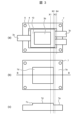
- FIG. 3 is an exploded plan view of the power semiconductor device of FIG. 2 .
- FIG. 5 is a cross-sectional view of a power semiconductor device according to a second embodiment of the present invention.
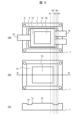
- FIG. 5 is an exploded plan view of the power semiconductor device of FIG. 4 .
- a semiconductor package 100 which serves as a semiconductor module in a power semiconductor device, includes a semiconductor element 1, a first conductor portion 3a, a second conductor portion 3b, and an external terminal 3c.
- the first conductor portion 3a and the second conductor portion 3b are thermally and electrically connected to the semiconductor element 1, and are made of, for example, copper, a copper alloy, aluminum, or an aluminum alloy.
- An electrode provided on one surface of the semiconductor element 1 is joined to the first conductor portion 3a by a bonding material 2.
- An electrode provided on the other surface of the semiconductor element 1 is joined to the second conductor portion 3b by the bonding material 2.
- the material of the bonding material 2 is, for example, a solder material, a sintered material, or the like.
- the first conductor 3a and the second conductor 3b are mold sealed such that the heat dissipation surface 10a, which is the surface opposite to the surface connected to the semiconductor element 1, is exposed from the sealing resin 10, which is the sealing member.
- This allows the semiconductor package 100 to dissipate heat generated in the semiconductor package 100 to the heat dissipation member 7, which will be described later, via the heat dissipation surfaces 10a exposed on both sides.
- the external terminal 3c is provided with a portion of the terminal protruding outward from the sealing member 10, allowing the semiconductor package 100 to be electrically connected to external wiring (not shown).
- the first conductor 3a is connected to the insulating plate 4, which is an insulating layer having electrical insulation properties, on the heat dissipation surface 10a via a heat conduction layer 5a made of a heat conductive material.
- the insulating plate 4 is connected to a heat conduction layer 5b made of a heat conductive material on the surface opposite to the surface to which the first conductor 3a is connected, and is connected to the heat dissipation member 7 via the heat conduction layer 5b.
- the second conductor 3b is connected to the insulating plate 4 on the heat dissipation surface 10a via the thermally conductive layer 5a.
- the insulating plate 4 is connected to the thermally conductive layer 5b on the surface opposite to the surface to which the second conductor 3b is connected, and is connected to the heat dissipation member 7. In this way, of the heat dissipation members 7 provided on both sides of the semiconductor package 100, the other heat dissipation member 7 faces the heat dissipation surface 10a of the second conductor 3b.
- the insulating plate 4 and the thermally conductive layers 5a and 5b sandwiching the insulating plate 4 are provided between the semiconductor package 100 and the heat dissipation member 7 and are in close contact with each other.
- a coolant flows inside the heat dissipation member 7, and the semiconductor package 100 ensures cooling by thermally conducting the heat generated by the semiconductor element 1 to the heat dissipation member 7 via the thermally conductive layers 5a and 5b and the insulating plate 4, and also electrically insulates the semiconductor package 100 from the heat dissipation member 7.
- the insulating plate 4 is an insulating sheet made of a material with high thermal conductivity and high dielectric strength, such as ceramics such as aluminum oxide (alumina), aluminum nitride, silicon nitride, etc., or fine powders of these materials.
- ceramics such as aluminum oxide (alumina), aluminum nitride, silicon nitride, etc., or fine powders of these materials.
- the thermal conductive layers 5a and 5b are provided with thermal conductive grease, TIM (Thermal Interface Material) and the like.
- thermally conductive material such as a heat dissipation sheet is used.
- the heat dissipation member 7 is made of a material having thermal conductivity, such as composite materials of Cu, Cu alloy, Cu-C, Cu-CuO, or composite materials of Al, Al alloy, AlSiC, Al-C, etc.
- the heat dissipation member 7 has a protruding portion 7c that protrudes toward the heat dissipation surface 10a of the first conductor portion 3a and the heat dissipation surface 10a of the second conductor portion 3b and has a protruding surface 7d that faces each of the heat dissipation surfaces 10a.
- the heat dissipation member 7 also has a recessed portion 7e that is provided around the protruding portion 7c in the planar direction and has a surface that is formed farther away from the insulating plate 4 than the protruding surface 7d in the stacking direction.
- the protruding surface 7d is formed larger in the planar direction than the opposing heat dissipation surface 10a, so that the heat dissipated from the heat dissipation surface 10a can be reliably absorbed by the heat dissipation member 7 and heat dissipation performance is not deteriorated.
- the heat dissipation member 7 is pressurized toward the semiconductor package 100 according to the arrow of the pressure applying portion 11.
- the ends of the first conductor portion 3a and the second conductor portion 3b in the planar direction are designated as X1, the end of the convex portion 7c of the heat dissipation member 7 in the planar direction is designated as X2, the end of the sealing resin 10 in the planar direction is designated as X3, and the end of the insulating plate 4 in the planar direction is designated as X4.
- End X2 is located outside end X1 in the planar direction, and inside end X3 of sealing member 10 in the planar direction.
- the recess 7e of heat dissipation member 7 is formed at a position where end X3 of sealing member 10 and insulating plate 4 overlap in a planar view.
- Insulating plate 4 is a white ceramic plate that does not have a wiring layer that forms a conductor on both sides, and its both sides are sandwiched between thermally conductive layers 5a and 5b, which contributes to suppressing cracks in insulating plate 4.
- FIG. 3(a) is a plan view of a semiconductor package 100 having the heat dissipation member 7 of FIG. 2 with the upper heat dissipation member 7, the first conductor portion 3a, and the semiconductor element 1 removed
- FIG. 3(b) is a plan view of the heat dissipation member 7 of FIG. 3(a)
- FIG. 3(c) is a cross-sectional view of the heat dissipation member 7 of FIG. 3(b).
- the heat dissipation member 7 has bolt holes 9 at each of the four corners as shown in FIG. 3.
- bolts (not shown) are inserted into the bolt holes 9, pressure is generated in the direction of the arrows of the pressure applying portion 11 (FIG. 2) of the heat dissipation member 7, and the heat dissipation member 7 is pressed toward the semiconductor package 100.
- the pressure applying portion 11 of the semiconductor package 100 may be formed at the position of the convex portion 7c of the heat dissipation member in the stacking direction.
- the semiconductor package 100 has external terminals 3c that protrude from the sealing member 10 to the outside, and the insulating plate 4 overlaps at least a portion of the external terminals 3c when viewed in a plan view. This increases the creepage distance between the external terminals 3c and the heat dissipation members 7 formed on both sides of the semiconductor package 100, improving the dielectric strength, and preventing dielectric breakdown even when the semiconductor package 100 is used at high voltage.
- the insulating plate 4 for ensuring the creepage distance does not have to be configured to be disposed over the entire surface in the planar direction as shown in FIG. 3, but may be formed only in the portion where the external terminals 3c protrude from the sealing member 10 to the outside.
- the heat conductive layer 5b is provided between the insulating plate 4 and the convex portion 7c, so that the convex portion 7c does not come into direct contact with the heat dissipation member 7 and acts as a stress relief layer.
- the heat dissipation member 7 undergoes bending deformation with the end portion X2 of the convex portion 7c as the fulcrum.
- the heat conductive layer 5b on the concave portion 7e which is affected by the stress caused by this deformation, is made thicker in the stacking direction by the step difference between the convex portion 7c and the concave portion 7e.
- the heat dissipation member 7 need not necessarily be made of a single member, but may be made of multiple members.
- the heat dissipation member 7 may also be provided with water channels through which a refrigerant flows, pin fins, corrugated fins, etc., inside, or may be air-cooled or have other cooling forms.
- Figure 5(a) is a plan view of a semiconductor package 100 equipped with the heat dissipation member 7 of Figure 4, with the upper heat dissipation member 7, first conductor portion 3a, and semiconductor element 1 removed in the stacking direction
- Figure 3(b) is a plan view of the heat dissipation member 7 of Figure 3(a)
- Figure 3(c) is a cross-sectional view of the heat dissipation member 7 of Figure 3(b).
- the recess 7e is formed so that, when viewed in a plan view, the recess 7e does not extend to the position of the bolt hole 9 of the heat dissipation member 7.
- the end X5 of the recess 7e in the planar direction is provided on the outer side of the end X4. This prevents the thickness of the heat dissipation member 7 from becoming thin around the bolt hole 9, which is the load-bearing portion for pressurizing the heat dissipation member 7 toward the semiconductor package 100, and therefore allows for efficient pressure application.
- a semiconductor package 100 having a semiconductor element 1, conductors 3a, 3b thermally and electrically connected to the semiconductor element 1, and a sealing member 10 that mold-seals the semiconductor element 1 and the conductors 3a, 3b, and in which a heat dissipation surface 10a, which is the surface of the conductors 3a, 3b opposite the surface that connects to the semiconductor element 1, is exposed from the sealing member 10, a heat dissipation member 7 arranged opposite the heat dissipation surface 10a, and an insulating plate 4 provided between the semiconductor package 100 and the heat dissipation member 7, and a portion of the insulating plate 4 is sealed in a planar direction.
- the heat dissipation member 10 is disposed at least outside the sealing member 10, and has a protruding portion 7c that protrudes toward the heat dissipation surface 10a and has a protruding surface 7d that faces the heat dissipation surface 10a, and a recessed portion 7e that is disposed around the protruding portion 7c in the planar direction and has a surface that is formed farther from the insulating plate 4 than the protruding surface 7d in the stacking direction, and the protruding surface 7d is formed larger in the planar direction than the heat dissipation surface 10a that is disposed opposite it, and the recessed portion 7e is formed at a position where the end X3 of the sealing member 10 and the insulating plate 4 overlap in a plan view.
- a highly reliable power semiconductor device that realizes stress reduction, improved dielectric strength, and improved heat dissipation can be provided.
- the insulating plate 4 is a white ceramic plate that does not have a wiring layer made of a conductor. By using such a material, it is possible to reduce stress and improve the dielectric strength.
- the semiconductor package 100 has terminals 3c that protrude from the sealing member 10 to the outside, and the insulating plate 4 overlaps at least a portion of the terminals 3c in a plan view. This ensures a creepage distance between the heat dissipation member 7 and the terminals 3c, improving the dielectric strength.
- a thermally conductive material is provided between the insulating plate 4 and the heat dissipation member 7. This allows the heat generated by the semiconductor package 100 to be transferred to the heat dissipation member 7 while electrically insulating the semiconductor package 100 from the heat dissipation member 7.
- a thermally conductive material is provided between the insulating plate 4 and the semiconductor package 100, or between the insulating plate 4 and the heat dissipation member 7. In this way, the semiconductor package 100 and the heat dissipation member 7 are electrically insulated from each other, while the heat generated by the semiconductor package 100 can be transferred to the heat dissipation member 7.
- the present invention is not limited to the above-described embodiment, and various modifications and other configurations can be combined without departing from the spirit of the invention. Furthermore, the present invention is not limited to those having all of the configurations described in the above-described embodiment, and also includes those in which some of the configurations have been omitted.
Landscapes
- Cooling Or The Like Of Semiconductors Or Solid State Devices (AREA)
Abstract
パワー半導体装置は、半導体素子と、前記半導体素子と熱的および電気的に接続された導体部と、前記半導体素子と前記導体部とをモールド封止する封止部材と、を有し、前記導体部において前記半導体素子と接続する面とは反対側の面である放熱面が前記封止部材から露出する半導体パッケージと、前記放熱面と対向して配置された放熱部材と、前記半導体パッケージと前記放熱部材との間に設けられる絶縁板と、を備え、前記絶縁板は、その一部が、平面方向において、前記封止部材よりも少なくとも外側に配置され、前記放熱部材は、前記放熱面に向かって突出し、前記放熱面と対向する突出面を設けている凸部と、平面方向において前記凸部の周囲に設けられ、積層方向において前記突出面と比べて前記絶縁板から離れて形成される面を設けている凹部と、を有し、前記突出面は、対向して配置される前記放熱面よりも平面方向において大きく形成され、前記凹部は、平面で見て、前記封止部材の端部と前記絶縁板が重なる位置に形成される。
Description
本発明は、パワー半導体装置に関する。
環境への負荷低減のため、ハイブリッド自動車や電気自動車の普及がすすめられ、例えば、これらの車両に搭載される部品の一つである電力変換装置におけるパワー半導体装置は、小型化や低コスト化が重視されている。発熱量が大きいパワー半導体装置を小型化するためには、冷却性能を向上させる必要がある。例えば特許文献1には、パワーモジュールが熱伝導部材と絶縁部材を介して冷却器が設けられ、パワーモジュール、熱伝導部材、冷却器が接続され、冷却性を確保したパワー半導体装置の構成が開示されている。
特許文献1に記載の技術において、パワーモジュールを高電圧対応にする場合、放熱部材と半導体モジュール外部端子と間の絶縁性を確保するため、絶縁部材を設ける。この絶縁部材は、放熱部材を加圧することで熱抵抗が低下して冷却性能を確保し、長期の信頼性を向上させている。しかしながら、セラミック板など絶縁耐圧の高い絶縁部材は加圧されることでクラックが発生する可能性があり、これにより信頼性が低下する課題が生じる。これを鑑みて本発明は、応力低減、絶縁耐圧の向上、放熱性の向上を実現した信頼性の高いパワー半導体装置を提供することが目的である。
パワー半導体装置は、半導体素子と、前記半導体素子と熱的および電気的に接続された導体部と、前記半導体素子と前記導体部とをモールド封止する封止部材と、を有し、前記導体部において前記半導体素子と接続する面とは反対側の面である放熱面が前記封止部材から露出する半導体パッケージと、前記放熱面と対向して配置された放熱部材と、前記半導体パッケージと前記放熱部材との間に設けられる絶縁板と、を備え、前記絶縁板は、その一部が、平面方向において、前記封止部材よりも少なくとも外側に配置され、前記放熱部材は、前記放熱面に向かって突出し、前記放熱面と対向する突出面を設けている凸部と、平面方向において前記凸部の周囲に設けられ、積層方向において前記突出面と比べて前記絶縁板から離れて形成される面を設けている凹部と、を有し、前記突出面は、対向して配置される前記放熱面よりも平面方向において大きく形成され、前記凹部は、平面で見て、前記封止部材の端部と前記絶縁板が重なる位置に形成される。
応力低減、絶縁耐圧の向上、放熱性の向上を実現した信頼性の高いパワー半導体装置を提供できる。
以下、図面を参照して本発明の実施形態を説明する。以下の記載および図面は、本発明を説明するための例示であって、説明の明確化のため、適宜、省略および簡略化がなされている。本発明は、他の種々の形態でも実施することが可能である。特に限定しない限り、各構成要素は単数でも複数でも構わない。
図面において示す各構成要素の位置、大きさ、形状、範囲などは、発明の理解を容易にするため、実際の位置、大きさ、形状、範囲などを表していない場合がある。このため、本発明は、必ずしも、図面に開示された位置、大きさ、形状、範囲などに限定されない。
(本発明の第1実施形態および全体構成)
(図1)
パワー半導体装置における半導体モジュールの役割を有する半導体パッケージ100は、半導体素子1、第1導体部3a、第2導体部3b、外部端子3cを有する。第1導体部3aおよび第2導体部3bは、半導体素子1と熱的および電気的に接続され、その材質は、例えば銅、銅合金、あるいはアルミニウム、アルミニウム合金などである。半導体素子1の一方の面に設けられる電極は、接合材2によって第1導体部3aと接合されている。半導体素子1の他方の面に設けられる電極は、接合材2によって第2導体部3bと接合されている。接合材2の材質は、例えば、はんだ材、焼結材などである。
(図1)
パワー半導体装置における半導体モジュールの役割を有する半導体パッケージ100は、半導体素子1、第1導体部3a、第2導体部3b、外部端子3cを有する。第1導体部3aおよび第2導体部3bは、半導体素子1と熱的および電気的に接続され、その材質は、例えば銅、銅合金、あるいはアルミニウム、アルミニウム合金などである。半導体素子1の一方の面に設けられる電極は、接合材2によって第1導体部3aと接合されている。半導体素子1の他方の面に設けられる電極は、接合材2によって第2導体部3bと接合されている。接合材2の材質は、例えば、はんだ材、焼結材などである。
第1導体部3aおよび第2導体部3bは、それぞれ半導体素子1と接続する面とは反対側の面である放熱面10aが封止部材である封止樹脂10から露出するように、モールド封止されている。これにより、半導体パッケージ100は、半導体パッケージ100で生じる熱を、その両面に露出している放熱面10aを介して後述の放熱部材7に放熱できる。外部端子3cは、その端子の一部が封止部材10から外部に突出して設けられており、これにより、半導体パッケージ100は図示しない外部の配線と電気的に接続できる。
(図2)
第1導体部3aは、放熱面10aにおいて、熱伝導性材料で形成される熱伝導層5aを介して電気絶縁性を有する絶縁層である絶縁板4と接続されている。この絶縁板4は、第1導体部3aが接続されている面とは反対の面で、熱伝導性材料で形成される熱伝導層5bと接続し、熱伝導層5bを介して放熱部材7に接続される。このように、半導体パッケージ100の両面に設けられている放熱部材7のうち、一方の放熱部材7は、第1導体部3aの放熱面10aと対向している。
第1導体部3aは、放熱面10aにおいて、熱伝導性材料で形成される熱伝導層5aを介して電気絶縁性を有する絶縁層である絶縁板4と接続されている。この絶縁板4は、第1導体部3aが接続されている面とは反対の面で、熱伝導性材料で形成される熱伝導層5bと接続し、熱伝導層5bを介して放熱部材7に接続される。このように、半導体パッケージ100の両面に設けられている放熱部材7のうち、一方の放熱部材7は、第1導体部3aの放熱面10aと対向している。
また、第2導体部3bは、放熱面10aにおいて、熱伝導層5aを介して絶縁板4と接続されている。この絶縁板4は、第2導体部3bが接続されている面とは反対の面で熱伝導層5bと接続し、放熱部材7に接続される。このように、半導体パッケージ100の両面に設けられている放熱部材7のうち、他方の放熱部材7は、第2導体部3bの放熱面10aと対向している。
絶縁板4およびこの絶縁板4を間に挟む熱伝導層5aおよび熱伝導層5bは、半導体パッケージ100と放熱部材7との間に設けられ、それぞれと密着している。これにより、放熱部材7は内部に冷媒が流通しており、半導体パッケージ100は半導体素子1から発生する熱を、熱伝導層5a,5b、絶縁板4を介して放熱部材7に熱伝導させることで冷却性を確保しており、かつ、半導体パッケージ100と放熱部材7とを電気的に絶縁している。
絶縁板4は、熱伝導率が高くかつ絶縁耐圧が大きい材料で形成されている絶縁シートであり、その材料は例えば、酸化アルミニウム(アルミナ)、窒化アルミニウム、窒化ケイ素等のセラミックス、あるいは、これらの微粉末を含有する。
熱伝導層5a,5bには、熱伝導グリス、TIM(Thermal Interface
Material)、あるいは放熱シートなどの熱伝導性を有する部材が用いられる。
Material)、あるいは放熱シートなどの熱伝導性を有する部材が用いられる。
放熱部材7には、熱伝導性を有する部材が用いられ、このような部材は例えば、Cu、Cu合金、Cu-C、Cu-CuOなどの複合材、あるいはAl、Al合金、AlSiC、Al-Cなどの複合材などである。
放熱部材7は、第1導体部3aの放熱面10aおよび第2導体部3bの放熱面10aそれぞれに向かって突出し、それぞれの放熱面10aと対向する突出面7dを設けている凸部7cを有する。また、放熱部材7は、平面方向において凸部7cの周囲に設けられ、積層方向において突出面7dと比べて絶縁板4から離れて形成される面を設けている凹部7eを有している。突出面7dは、対向する放熱面10aよりも平面方向において大きく形成されていることで、放熱面10aから放出される熱を確実に放熱部材7へ吸収することができ、放熱性能を悪化させることがない。放熱部材7は、加圧部11の矢印に従って半導体パッケージ100に向かって加圧されている。
第1導体部3aおよび第2導体部3bの平面方向における端部をX1、放熱部材7の凸部7cの平面方向における端部をX2、封止樹脂10の平面方向における端部をX3、絶縁板4の平面方向における端部をX4とする。
端部X2は、端部X1よりも平面方向において外側の位置に設けられており、かつ、封止部材10の端部X3より平面方向において内側になるように設けられている。放熱部材7の凹部7eは、平面で見て、封止部材10の端部X3と絶縁板4が重なる位置に形成されている。
絶縁板4の端部X4は、封止樹脂10の端部X3よりも外側に配置され、絶縁板4は少なくともその一部が、平面方向において封止樹脂10よりも外側に設けられている。絶縁板4は、両面に導体を形成する配線層を設けていないセラミック白板であり、熱伝導層5a,5bによってその両面が挟まれることで、絶縁板4のクラックの抑制に貢献する。
(図3)
図3(a)は図2の放熱部材7を備えた半導体パッケージ100から、上部の放熱部材7と第1導体部3aと半導体素子1を取り除いた平面図、図3(b)は図3(a)の放熱部材7の平面図、図3(c)は図3(b)の放熱部材7の断面図である。
図3(a)は図2の放熱部材7を備えた半導体パッケージ100から、上部の放熱部材7と第1導体部3aと半導体素子1を取り除いた平面図、図3(b)は図3(a)の放熱部材7の平面図、図3(c)は図3(b)の放熱部材7の断面図である。
放熱部材7は、図3に示すように四隅にそれぞれボルト穴9を有している。放熱部材7は、図示しないボルトがボルト穴9に挿入されることで、加圧部11(図2)の矢印の加圧が発生し放熱部材7を半導体パッケージ100に向かって加圧される。なお、放熱部材7が半導体パッケージ100に向かって加圧される構造であれば、ボルトに限らずクリップや板バネなどを用いてもよい。また、半導体パッケージ100の加圧部11は、積層方向において放熱部材の凸部7cの位置に形成されていてもよい。
半導体パッケージ100は、封止部材10から外部に突出する外部端子3cを有しているが、絶縁板4は、平面で見て少なくともその一部が外部端子3cと重なる。このようにすることで、外部端子3cと半導体パッケージ100の両面に形成される放熱部材7との間の沿面距離を増加させて絶縁耐圧が向上し、半導体パッケージ100を高電圧で使用する場合でも絶縁破壊を防止できる。なお、沿面距離を確保するための絶縁板4は、図3に示すように平面方向に全面配置されている構成ではなく、外部端子3cが封止部材10から外部に突出している部分に限定して形成されていてもよい。
絶縁板4と凸部7cの間には熱伝導層5bが設けられていることで、凸部7cが直接放熱部材7に接することがないため、応力緩和層として作用する。ここで、放熱部材7の加圧部11に荷重を負荷すると、放熱部材7には凸部7cの端部X2を支点にして曲げ変形が生じる。この変形による応力の影響がある凹部7e上の熱伝導層5bは、凸部7cと凹部7eとの間の段差分だけ積層方向に厚く設けられている。これにより、加圧部11に加圧しても、絶縁板4に応力がかかりにくくなるため絶縁板4のクラックは抑制される。
なお、放熱部材7は、単一部材で構成されたものだけでなく、複数の部材から構成されていてもよい。また、放熱部材7は内部に冷媒が流通する水路や、ピンフィンやコルゲートフィンなどが設けられていてもよく、空冷などその他の冷却形態であってもよい。
(第2実施形態)
(図4、図5)
図5(a)は図4の放熱部材7を備えた半導体パッケージ100から、積層方向において上部の放熱部材7と第1導体部3aと半導体素子1を取り除いた平面図、図3(b)は図3(a)の放熱部材7の平面図、図3(c)は図3(b)の放熱部材7の断面図である。
(図4、図5)
図5(a)は図4の放熱部材7を備えた半導体パッケージ100から、積層方向において上部の放熱部材7と第1導体部3aと半導体素子1を取り除いた平面図、図3(b)は図3(a)の放熱部材7の平面図、図3(c)は図3(b)の放熱部材7の断面図である。
図5(a)に示すように、凹部7eは、平面で見た場合、放熱部材7のボルト穴9の位置まで凹部7eの範囲が広がらないように形成されている。なお、平面方向における凹部7eの端部X5は、端部X4よりも外部側に設けられている。このようにすることで、放熱部材7を半導体パッケージ100側に加圧するための荷重負荷部分であるボルト穴9の周囲において、放熱部材7の肉厚が薄くなるのを防止できるため、効率よく加圧することができる。
以上説明した本発明の実施形態によれば、以下の作用効果を奏する。
(1)半導体素子1と、半導体素子1と熱的および電気的に接続された導体3a,3bと、半導体素子1と導体3a,3bとをモールド封止する封止部材10と、を有し、導体3a,3bにおいて半導体素子1と接続する面とは反対側の面である放熱面10aが封止部材10から露出する半導体パッケージ100と、放熱面10aと対向して配置された放熱部材7と、半導体パッケージ100と放熱部材7との間に設けられる絶縁板4と、を備え、絶縁板4は、その一部が、平面方向において、封止部材10よりも少なくとも外側に配置され、放熱部材10は、放熱面10aに向かって突出し、放熱面10aと対向する突出面7dを設けている凸部7cと、平面方向において凸部7cの周囲に設けられ、積層方向において突出面7dと比べて絶縁板4から離れて形成される面を設けている凹部7eと、を有し、突出面7dは、対向して配置される放熱面10aよりも平面方向において大きく形成され、凹部7eは、平面で見て、封止部材10の端部X3と絶縁板4が重なる位置に形成される。このようにしたことで、応力低減、絶縁耐圧の向上、放熱性の向上を実現した信頼性の高いパワー半導体装置を提供できる。
(2)絶縁板4は、導体で形成される配線層を設けないセラミック白板である。このような部材を用いたことで、応力低減、絶縁耐圧の向上が実現できる。
(3)半導体パッケージ100は、封止部材10から外部に突出する端子部3cを有し、絶縁板4は、平面で見て、少なくともその一部が端子部3cと重なる。このようにしたことで、放熱部材7と端子部3cとの沿面距離を確保し、絶縁耐圧が向上する。
(4)絶縁板4と放熱部材7の間には、熱伝導性材料が設けられている。このようにしたことで、半導体パッケージ100と放熱部材7との間を電気的に絶縁しつつ、半導体パッケージ100から発生する熱を放熱部材7に伝熱できる。
(5)絶縁板4と半導体パッケージ100の間、または絶縁板4と放熱部材7の間には、熱伝導性材料が設けられている。このようにしたことで、半導体パッケージ100と放熱部材7との間を電気的に絶縁しつつ、半導体パッケージ100から発生する熱を放熱部材7に伝熱できる。
なお、本発明は上記の実施形態に限定されるものではなく、その要旨を逸脱しない範囲内で様々な変形や他の構成を組み合わせることができる。また本発明は、上記の実施形態で説明した全ての構成を備えるものに限定されず、その構成の一部を削除したものも含まれる。
1 半導体素子
2 接合材
3a 第1導体部
3b 第2導体部
3c 外部端子
4 絶縁板
5a,5b 熱伝導層
7 放熱部材
7c 放熱部材の凸部
7d 突出面
7e 放熱部材の凹部
9 ボルト穴
10 封止樹脂
10a 放熱面
11 加圧部
X1 導体部の端部
X2 放熱部材の凸部の端部
X3 封止樹脂の端部
X4 絶縁板の端部
X5 放熱部材の凹部の端部
100 半導体パッケージ
2 接合材
3a 第1導体部
3b 第2導体部
3c 外部端子
4 絶縁板
5a,5b 熱伝導層
7 放熱部材
7c 放熱部材の凸部
7d 突出面
7e 放熱部材の凹部
9 ボルト穴
10 封止樹脂
10a 放熱面
11 加圧部
X1 導体部の端部
X2 放熱部材の凸部の端部
X3 封止樹脂の端部
X4 絶縁板の端部
X5 放熱部材の凹部の端部
100 半導体パッケージ
Claims (5)
- 半導体素子と、前記半導体素子と熱的および電気的に接続された導体部と、前記半導体素子と前記導体部とをモールド封止する封止部材と、を有し、前記導体部において前記半導体素子と接続する面とは反対側の面である放熱面が前記封止部材から露出する半導体パッケージと、
前記放熱面と対向して配置された放熱部材と、
前記半導体パッケージと前記放熱部材との間に設けられる絶縁板と、を備え、
前記絶縁板は、その一部が、平面方向において、前記封止部材よりも少なくとも外側に配置され、
前記放熱部材は、前記放熱面に向かって突出し、前記放熱面と対向する突出面を設けている凸部と、平面方向において前記凸部の周囲に設けられ、積層方向において前記突出面と比べて前記絶縁板から離れて形成される面を設けている凹部と、を有し、
前記突出面は、対向して配置される前記放熱面よりも平面方向において大きく形成され、
前記凹部は、平面で見て、前記封止部材の端部と前記絶縁板が重なる位置に形成される
パワー半導体装置。 - 請求項1に記載されたパワー半導体装置であって、
前記絶縁板は、導体で形成される配線層を設けないセラミック白板である
パワー半導体装置。 - 請求項1に記載されたパワー半導体装置であって、
前記半導体パッケージは、前記封止部材から外部に突出する端子部を有し、
前記絶縁板は、平面で見て、少なくともその一部が前記端子部と重なる
パワー半導体装置。 - 請求項1に記載されたパワー半導体装置であって、
前記絶縁板と前記放熱部材の間には、熱伝導性材料が設けられている
パワー半導体装置。 - 請求項1に記載されたパワー半導体装置であって、
前記絶縁板と前記半導体パッケージの間、または前記絶縁板と前記放熱部材の間には、熱伝導性材料が設けられている
パワー半導体装置。
Applications Claiming Priority (2)
| Application Number | Priority Date | Filing Date | Title |
|---|---|---|---|
| JP2023-201955 | 2023-11-29 | ||
| JP2023201955A JP2025087361A (ja) | 2023-11-29 | 2023-11-29 | パワー半導体装置 |
Publications (1)
| Publication Number | Publication Date |
|---|---|
| WO2025115274A1 true WO2025115274A1 (ja) | 2025-06-05 |
Family
ID=95896636
Family Applications (1)
| Application Number | Title | Priority Date | Filing Date |
|---|---|---|---|
| PCT/JP2024/024610 Pending WO2025115274A1 (ja) | 2023-11-29 | 2024-07-08 | パワー半導体装置 |
Country Status (2)
| Country | Link |
|---|---|
| JP (1) | JP2025087361A (ja) |
| WO (1) | WO2025115274A1 (ja) |
Citations (8)
| Publication number | Priority date | Publication date | Assignee | Title |
|---|---|---|---|---|
| JP2005012163A (ja) * | 2003-05-26 | 2005-01-13 | Denso Corp | 半導体装置 |
| JP2005117009A (ja) * | 2003-09-17 | 2005-04-28 | Denso Corp | 半導体装置およびその製造方法 |
| JP2016076563A (ja) * | 2014-10-06 | 2016-05-12 | 日立オートモティブシステムズ株式会社 | パワーモジュール及び電力変換装置 |
| JP2019125700A (ja) * | 2018-01-17 | 2019-07-25 | 日立オートモティブシステムズ株式会社 | パワー半導体装置 |
| WO2020079801A1 (ja) * | 2018-10-18 | 2020-04-23 | 三菱電機株式会社 | 基板収納筐体 |
| JP2021182568A (ja) * | 2020-05-18 | 2021-11-25 | 日立Astemo株式会社 | パワーモジュール |
| JP2022098587A (ja) * | 2020-12-22 | 2022-07-04 | 日立Astemo株式会社 | 電気回路体および電力変換装置 |
| WO2023223804A1 (ja) * | 2022-05-16 | 2023-11-23 | 三菱電機株式会社 | パワーモジュール、パワーモジュールの製造方法、および電力変換装置 |
-
2023
- 2023-11-29 JP JP2023201955A patent/JP2025087361A/ja active Pending
-
2024
- 2024-07-08 WO PCT/JP2024/024610 patent/WO2025115274A1/ja active Pending
Patent Citations (8)
| Publication number | Priority date | Publication date | Assignee | Title |
|---|---|---|---|---|
| JP2005012163A (ja) * | 2003-05-26 | 2005-01-13 | Denso Corp | 半導体装置 |
| JP2005117009A (ja) * | 2003-09-17 | 2005-04-28 | Denso Corp | 半導体装置およびその製造方法 |
| JP2016076563A (ja) * | 2014-10-06 | 2016-05-12 | 日立オートモティブシステムズ株式会社 | パワーモジュール及び電力変換装置 |
| JP2019125700A (ja) * | 2018-01-17 | 2019-07-25 | 日立オートモティブシステムズ株式会社 | パワー半導体装置 |
| WO2020079801A1 (ja) * | 2018-10-18 | 2020-04-23 | 三菱電機株式会社 | 基板収納筐体 |
| JP2021182568A (ja) * | 2020-05-18 | 2021-11-25 | 日立Astemo株式会社 | パワーモジュール |
| JP2022098587A (ja) * | 2020-12-22 | 2022-07-04 | 日立Astemo株式会社 | 電気回路体および電力変換装置 |
| WO2023223804A1 (ja) * | 2022-05-16 | 2023-11-23 | 三菱電機株式会社 | パワーモジュール、パワーモジュールの製造方法、および電力変換装置 |
Also Published As
| Publication number | Publication date |
|---|---|
| JP2025087361A (ja) | 2025-06-10 |
Similar Documents
| Publication | Publication Date | Title |
|---|---|---|
| CN113039636B (zh) | 功率半导体装置 | |
| US9870974B2 (en) | Power conversion apparatus including wedge inserts | |
| JP2005012163A (ja) | 半導体装置 | |
| JP7734631B2 (ja) | 電気回路体および電力変換装置 | |
| US9209099B1 (en) | Power semiconductor module | |
| US11735557B2 (en) | Power module of double-faced cooling | |
| CN104798194B (zh) | 半导体器件 | |
| JP2023112990A (ja) | 半導体装置 | |
| JP2019134018A (ja) | 半導体装置 | |
| JP4046623B2 (ja) | パワー半導体モジュールおよびその固定方法 | |
| JP7580349B2 (ja) | パワー半導体装置 | |
| US12283536B2 (en) | Power semiconductor device and manufacturing method of power semiconductor device | |
| CN114388456A (zh) | 具有导热装置的功率电子开关装置及其生产方法 | |
| JP2025087361A (ja) | パワー半導体装置 | |
| CN120476471A (zh) | 功率半导体装置 | |
| JP7587454B2 (ja) | パワー半導体装置 | |
| JP3394000B2 (ja) | モジュール型半導体装置及びこれを用いた電力変換装置 | |
| US20250096069A1 (en) | Power module and method of fabricating the same | |
| WO2026028383A1 (ja) | 電力変換装置、電力変換装置の製造方法 | |
| CN121693847A (zh) | 电力转换装置 | |
| JP2007109857A (ja) | 半導体モジュールの絶縁構造 | |
| WO2025173129A1 (ja) | 半導体装置 | |
| KR20240109845A (ko) | 양면 냉각 파워 모듈 및 이의 제조방법 | |
| JP2026010714A (ja) | 接続導体の冷却装置 | |
| WO2026099990A1 (ja) | 半導体装置 |
Legal Events
| Date | Code | Title | Description |
|---|---|---|---|
| 121 | Ep: the epo has been informed by wipo that ep was designated in this application |
Ref document number: 24896966 Country of ref document: EP Kind code of ref document: A1 |
|
| NENP | Non-entry into the national phase |
Ref country code: DE |