WO2025069737A1 - 光検出装置及び電子機器 - Google Patents
光検出装置及び電子機器 Download PDFInfo
- Publication number
- WO2025069737A1 WO2025069737A1 PCT/JP2024/028561 JP2024028561W WO2025069737A1 WO 2025069737 A1 WO2025069737 A1 WO 2025069737A1 JP 2024028561 W JP2024028561 W JP 2024028561W WO 2025069737 A1 WO2025069737 A1 WO 2025069737A1
- Authority
- WO
- WIPO (PCT)
- Prior art keywords
- semiconductor layer
- photoelectric conversion
- region
- pixel
- gate electrode
- Prior art date
- Legal status (The legal status is an assumption and is not a legal conclusion. Google has not performed a legal analysis and makes no representation as to the accuracy of the status listed.)
- Pending
Links
Images



























Classifications
-
- H—ELECTRICITY
- H04—ELECTRIC COMMUNICATION TECHNIQUE
- H04N—PICTORIAL COMMUNICATION, e.g. TELEVISION
- H04N25/00—Circuitry of solid-state image sensors [SSIS]; Control thereof
- H04N25/70—SSIS architectures; Circuits associated therewith
-
- H—ELECTRICITY
- H04—ELECTRIC COMMUNICATION TECHNIQUE
- H04N—PICTORIAL COMMUNICATION, e.g. TELEVISION
- H04N25/00—Circuitry of solid-state image sensors [SSIS]; Control thereof
- H04N25/70—SSIS architectures; Circuits associated therewith
- H04N25/79—Arrangements of circuitry being divided between different or multiple substrates, chips or circuit boards, e.g. stacked image sensors
Definitions
- This technology (the technology disclosed herein) relates to photodetection devices and electronic devices, and in particular to technology that is effective when applied to photodetection devices having transfer transistors and electronic devices equipped with the same.
- Photodetection devices such as solid-state imaging devices and distance measuring devices have a transfer transistor for each pixel that transfers the signal charge photoelectrically converted in the photoelectric conversion section to a charge storage section.
- Patent Document 1 discloses a vertical structure transfer transistor in which a part of a gate electrode (transfer gate section) is provided in a recessed section of a semiconductor substrate (semiconductor layer) with a gate insulating film interposed therebetween.
- the entire periphery of the transfer gate portion of the gate electrode is adjacent to the semiconductor substrate with the gate insulating film interposed between them. This causes a capacitance component (parasitic capacitance) with the semiconductor substrate to be added to the entire periphery of the transfer gate portion of the gate electrode. If this capacitance component is large, the drive pulse applied to the gate electrode of the transfer transistor becomes dull, and the transfer speed (pixel drive speed) for transferring signal charges from the photoelectric conversion portion to the charge storage portion decreases. Furthermore, the decrease in transfer speed affects the performance of the photodetection device, so the capacitance component cannot be ignored.
- the purpose of this technology is to provide technology that can improve the performance of optical detection devices.
- a photodetector a semiconductor layer having a first surface portion and a second surface portion positioned opposite to each other in one direction; an insulator provided on the first surface side of the semiconductor layer; a photoelectric conversion unit that photoelectrically converts light incident from the second surface side of the semiconductor layer into a signal charge; a charge retaining portion provided on the first surface side of the semiconductor layer; a transfer transistor that transfers the signal charge photoelectrically converted by the photoelectric conversion unit to the charge storage unit; It is equipped with: The transfer transistor has a gate electrode adjacent to each of the semiconductor layer and the insulator, and extending in the one direction.
- a photodetector a semiconductor layer having a first surface portion and a second surface portion positioned opposite to each other in one direction; a photoelectric conversion region provided in the semiconductor layer and partitioned by a separation region extending in the one direction; It is equipped with: The photoelectric conversion region is an internal separation barrier extending in one direction; a first photoelectric conversion cell and a second photoelectric conversion cell arranged adjacent to each other with the internal isolation barrier interposed therebetween in a direction intersecting the one direction, Each of the first and second photoelectric conversion cells has a photoelectric conversion portion and a charge holding portion that holds signal charges photoelectrically converted by the photoelectric conversion portion.
- the internal isolation barrier protrudes from one of the two isolation regions located on opposite sides of the photoelectric conversion region in a plan view toward the other isolation region,
- the charge holding portions of the first and second photoelectric conversion cells are adjacent to each other on one of the isolation regions via the internal isolation barrier.
- a photodetector a semiconductor layer having a first surface portion and a second surface portion positioned opposite to each other in one direction; an isolation region extending from the first surface portion of the semiconductor layer toward the second surface portion; a transfer transistor provided on the first surface side of the semiconductor layer and configured to transfer the signal charge photoelectrically converted by the photoelectric conversion unit to a charge holding unit; It is equipped with:
- the transfer transistor has a gate electrode provided on the outer side of the first surface portion of the semiconductor layer, spanning the semiconductor layer and the isolation region in a plan view.
- An electronic device includes: The photodetector; an optical lens that forms an image of image light from a subject on an imaging surface of the light detection device; a signal processing circuit for processing a signal output from the photodetector; It is equipped with:
- FIG. 1 is a chip layout diagram showing a configuration example of a solid-state imaging device according to a first embodiment of the present technology.
- 1 is a block diagram showing a configuration example of a solid-state imaging device according to a first embodiment of the present technology.
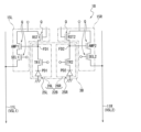
- 1 is an equivalent circuit diagram showing a configuration example of a pixel and a pixel circuit according to a first embodiment of the present technology.
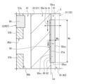
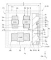
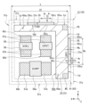
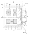
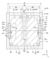
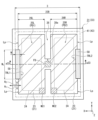
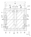
- 1 is a plan view illustrating a schematic configuration example of one pixel in a solid-state imaging device according to a first embodiment of the present technology;
- FIG. 4B is an enlarged plan view of a portion of FIG. 4A.
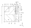
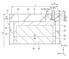
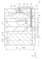
- 4B is a longitudinal sectional view showing a schematic longitudinal sectional structure taken along the a4-a4 cutting line in FIG. 4A.
- FIG. 5B is an enlarged plan view of a portion of FIG. 5A.
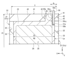
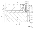
- 4B is a longitudinal sectional view showing a schematic longitudinal sectional structure taken along the b4-b4 cutting line in FIG. 4A.
- 3A to 3C are longitudinal cross-sectional views each showing a schematic process of a method for manufacturing a solid-state imaging device according to a first embodiment of the present technology.
- FIG. 7B is a vertical cross-sectional view showing a schematic process following FIG. 7A.
- FIG. 7C is a vertical cross-sectional view showing a schematic diagram of a step following FIG. 7B.
- FIG. 7D is a vertical cross-sectional view showing a schematic process following FIG. 7C.
- FIG. 7B is a vertical cross-sectional view showing a schematic process following FIG.
- FIG. 1 is a diagram showing a modified example 1-1 according to the first embodiment of the present technology, and is a plan view diagrammatically showing one pixel.
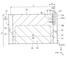
- 8B is a longitudinal sectional view showing a schematic longitudinal sectional structure taken along the a8-a8 cutting line in FIG. 8A.
- FIG. 13 is a diagram showing Modification 1-2 according to the first embodiment of the present technology, and is a plan view diagrammatically showing one pixel.
- 9B is a longitudinal sectional view showing a schematic longitudinal sectional structure taken along the a9-a9 cutting line in FIG. 9A.
- FIG. 11 is a diagram showing Modification 1-3 according to the first embodiment of the present technology, and is a plan view showing one pixel in schematic form.
- FIG. 10B is a longitudinal sectional view showing a schematic longitudinal sectional structure taken along the a10-a10 cutting line in FIG. 10A.
- FIG. 13 is a diagram showing a modified example 1-4 according to the first embodiment of the present technology, and is a plan view showing one pixel in schematic form.
- 11B is a longitudinal sectional view showing a schematic longitudinal sectional structure taken along the a11-a11 cutting line in FIG. 11A.
- FIG. 13 is a diagram showing Modification 1-5 according to the first embodiment of the present technology, and is a plan view showing one pixel in schematic form.
- 12B is a longitudinal sectional view showing a schematic longitudinal sectional structure taken along the a12-a12 cutting line in FIG. 12A.
- FIG. 13 is a diagram showing a modified example 1-6 according to the first embodiment of the present technology, and is a plan view showing one pixel in schematic form.
- FIG. 13 is a diagram showing Modification 1-7 according to the first embodiment of the present technology, and is a plan view diagrammatically showing one pixel.
- FIG. 13 is a diagram showing Modification 1-8 according to the first embodiment of the present technology, and is a plan view showing one pixel in schematic form.
- FIG. 13 is a diagram showing Modification 1-9 according to the first embodiment of the present technology, and is a plan view showing one pixel in schematic form.
- FIG. 10 is a diagram showing a modified example 1-10 according to the first embodiment of the present technology, and is a plan view showing one pixel in schematic form.
- FIG. 17B is a longitudinal sectional view showing a schematic longitudinal sectional structure taken along the a17-a17 cutting line in FIG. 17A.
- FIG. 11 is a diagram showing Modification 1-11 according to the first embodiment of the present technology, and is a plan view showing one pixel in schematic form.
- 17B is a longitudinal sectional view showing a schematic longitudinal sectional structure taken along the a17-a17 cutting line in FIG. 17A.
- FIG. 13 is a diagram showing Modification 1-12 according to the first embodiment of the present technology, and is a plan view diagrammatically showing one pixel.
- FIG. 13 is a diagram showing Modification 1-13 according to the first embodiment of the present technology, and is a plan view diagrammatically showing one pixel.
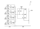
- FIG. 11 is an equivalent circuit diagram illustrating a configuration example of a pixel and a pixel circuit in a solid-state imaging device according to a second embodiment of the present technology.
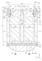
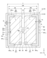
- FIG. 13 is a plan view illustrating a schematic configuration example of one pixel in a solid-state imaging device according to a second embodiment of the present technology.
- FIG. 20B is a longitudinal sectional view showing a schematic longitudinal sectional structure taken along the a20-a20 cutting line in FIG. 20B.
- FIG. 13 is a diagram showing a modified example 2-1 according to the second embodiment of the present technology, and is a plan view diagrammatically showing a configuration example of one pixel.
- 21B is a longitudinal sectional view showing a schematic longitudinal sectional structure taken along the a21-a21 cutting line in FIG.
- 21A. 21B is a longitudinal cross-sectional view showing a schematic longitudinal cross-sectional structure taken along the b21-b21 cutting line in FIG. 21A.
- FIG. 13 is a diagram showing a modified example 2-2 according to the second embodiment of the present technology, and is a plan view diagrammatically showing a configuration example of one pixel.
- 22B is a longitudinal sectional view showing a schematic longitudinal sectional structure taken along the a22-a22 cutting line in FIG. 22A.
- FIG. 13 is a diagram showing a modified example 2-3 according to the second embodiment of the present technology, and is a plan view diagrammatically showing a configuration example of one pixel.
- 23B is a longitudinal sectional view showing a schematic longitudinal sectional structure taken along the a23-a23 cutting line in FIG.
- FIG. 13 is a diagram showing a modified example 2-4 according to the second embodiment of the present technology, and is a plan view diagrammatically showing a configuration example of one pixel.
- 24B is a longitudinal sectional view showing a schematic longitudinal sectional structure taken along the a24-a24 cutting line in FIG. 24A.
- FIG. 13 is a diagram showing a modified example 2-5 according to the second embodiment of the present technology, and is a plan view showing one pixel in schematic form.
- FIG. 13 is a diagram showing a modified example 2-6 according to the second embodiment of the present technology, and is a plan view diagrammatically showing a configuration example of one pixel.
- 26B is a longitudinal sectional view showing a schematic longitudinal sectional structure taken along the a26-a26 cutting line in FIG. 26A.
- FIG. 13 is a diagram showing a modified example 2-7 according to the second embodiment of the present technology, and is a plan view diagrammatically showing a configuration example of one pixel.
- 27B is a longitudinal cross-sectional view showing a schematic longitudinal cross-sectional structure taken along the a27-a27 cutting line in FIG. 27A.
- FIG. 13 is a diagram showing a modified example 2-8 according to the second embodiment of the present technology, and is a plan view showing one pixel in schematic form.
- FIG. 13 is a diagram showing a modified example 2-9 according to the second embodiment of the present technology, and is a plan view showing one pixel in schematic form.
- FIG. 13 is a diagram showing a modified example 2-10 of the second embodiment of the present technology, and is a plan view showing one pixel in schematic form.
- FIG. 11 is a diagram showing a modified example 2-11 according to the second embodiment of the present technology, and is a plan view showing one pixel in schematic form.
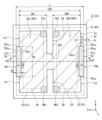
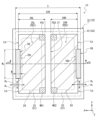
- FIG. 13 is a plan view illustrating a schematic configuration example of one pixel in a solid-state imaging device according to a third embodiment of the present technology.
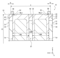
- FIG. 32B is a longitudinal cross-sectional view showing a schematic longitudinal cross-sectional structure taken along the a32-a32 cutting line in FIG. 32A.
- FIG. 13 is a diagram showing a modified example 3-1 according to the third embodiment of the present technology, and is a plan view diagrammatically showing a configuration example of one pixel.
- 33B is a longitudinal cross-sectional view showing a schematic longitudinal cross-sectional structure taken along the a33-a33 cutting line in FIG. 33A.
- FIG. 13 is a diagram illustrating a modified example 3-2 according to the third embodiment of the present technology, and is a plan view diagrammatically illustrating a configuration example of one pixel.
- FIG. 34B is a longitudinal sectional view showing a schematic longitudinal sectional structure taken along the a34-a34 cutting line in FIG. 34A.
- FIG. 13 is a diagram illustrating a modified example 3-3 according to the third embodiment of the present technology, and is a plan view diagrammatically illustrating a configuration example of one pixel.
- 35B is a longitudinal cross-sectional view showing a schematic longitudinal cross-sectional structure taken along the a35-a35 cutting line in FIG. 35A.
- 13 is a plan view illustrating a schematic configuration example of one pixel in a solid-state imaging device according to a fourth embodiment of the present technology.
- FIG. 36B is a longitudinal cross-sectional view showing a schematic longitudinal cross-sectional structure taken along the a36-a36 cutting line in FIG.
- FIG. 13 is an exploded view illustrating a schematic configuration example of a solid-state imaging device according to a fifth embodiment of the present technology.
- FIG. 13 is an equivalent circuit diagram showing a configuration example of a pixel and a pixel circuit according to a fifth embodiment of the present technology.
- FIG. 13 is a diagram showing a schematic configuration of an electronic device according to a sixth embodiment of the present technology.
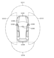
- FIG. 23 is a block diagram showing an example of a schematic configuration of a vehicle control system according to a seventh embodiment of the present technology. 4 is an explanatory diagram showing an example of the installation positions of an outside-vehicle information detection unit and an imaging unit;
- FIG. FIG. 23 is a diagram showing an example of a schematic configuration of an endoscopic surgery system according to an eighth embodiment of the present technology.
- 2 is a block diagram showing an example of the functional configuration of a camera head and a CCU.
- up and down and other directions in the following explanation are merely for the convenience of explanation and do not limit the technical ideas of this technology. For example, if an object is rotated 90 degrees and observed, up and down are converted into left and right and read, and of course, if it is rotated 180 degrees and observed, up and down are read inverted.
- a first direction and a second direction mutually orthogonal in the same plane are defined as an X direction and a Y direction, respectively, and a third direction perpendicular to each of the first direction and the second direction is defined as a Z direction.
- the thickness direction of a semiconductor layer 21 described later will be described as the Z direction.
- the Z direction will be described as "one direction" of the present technology.
- the thickness of the semiconductor layer 21 is the distance between the first surface portion S1 and the second surface portion S2, which are located on opposite sides in the Z direction, and the thickness direction of the semiconductor layer 21 is the direction that represents the thickness of the semiconductor layer 21.
- a planar view refers to the semiconductor layer 21 being viewed from the Z direction (one direction).
- a cross-sectional view refers to the cross section along the Z direction (one direction) being viewed from a direction perpendicular to the Z direction.
- CMOS complementary metal oxide semiconductor
- the solid-state imaging device 1A is mainly composed of a semiconductor chip 2 having a rectangular two-dimensional planar shape when viewed in a plane. That is, the solid-state imaging device 1A is mounted on the semiconductor chip 2, and the semiconductor chip 2 can be regarded as the solid-state imaging device 1A. As shown in Fig. 1, the solid-state imaging device 1A according to the first embodiment of the present technology is mainly composed of a semiconductor chip 2 having a rectangular two-dimensional planar shape when viewed in a plane. That is, the solid-state imaging device 1A is mounted on the semiconductor chip 2, and the semiconductor chip 2 can be regarded as the solid-state imaging device 1A. As shown in Fig.
- this solid-state imaging device 1A takes in image light (incident light 306) from a subject via an optical lens 302, converts the amount of incident light 306 formed on an imaging surface into an electrical signal on a pixel-by-pixel basis, and outputs the electrical signal as a pixel signal.
- the semiconductor chip 2 on which the solid-state imaging device 1A is mounted has a square pixel array section 2A located in the center of a two-dimensional plane including mutually orthogonal X and Y directions, and a peripheral section 2B located outside the pixel array section 2A so as to surround the pixel array section 2A.
- the semiconductor chip 2 is formed in the manufacturing process by dicing a semiconductor wafer including a semiconductor layer 21 described below into chip formation regions. Therefore, the configuration of the solid-state imaging device 1A described below is generally the same in the wafer state before the semiconductor wafer is diced. Therefore, this technology can be applied in the semiconductor chip state and in the semiconductor wafer state.
- the pixel array section 2A shown in FIG. 1 is, for example, a light receiving surface that receives light collected by an optical lens (optical system) 302 shown in FIG. 39.
- a plurality of pixels 3 (sensor pixels) are arranged in a matrix on a two-dimensional plane including the X direction and the Y direction.
- the pixels 3 are repeatedly arranged in each of the X direction and the Y direction that are mutually orthogonal within the two-dimensional plane.
- a plurality of bonding pads 14 are arranged in the peripheral portion 2B.
- Each of the plurality of bonding pads 14 is arranged, for example, along each of the four sides of the semiconductor chip 2 in a two-dimensional plane.
- Each of the plurality of bonding pads 14 functions as an input/output terminal that electrically connects the semiconductor chip 2 to an external device.
- the semiconductor chip 2 includes a logic circuit 13 shown in Fig. 2.
- the logic circuit 13 includes a vertical drive circuit 4, a column signal processing circuit 5, a horizontal drive circuit 6, an output circuit 7, and a control circuit 8.
- the logic circuit 13 is configured of a CMOS (Complementary MOS) circuit having, as field effect transistors, for example, n-channel conductivity type MOSFETs (Metal Oxide Semiconductor Field Effect Transistors) and p-channel conductivity type MOSFETs.
- CMOS Complementary MOS
- the vertical drive circuit 4 shown in FIG. 2 is composed of, for example, a shift register.
- the vertical drive circuit 4 sequentially selects the desired pixel drive lines 10, supplies pulses to the selected pixel drive lines 10 for driving the pixels 3, and drives each pixel 3 row by row. That is, the vertical drive circuit 4 sequentially selects and scans each pixel 3 in the pixel array section 2A vertically row by row, and supplies pixel signals from the pixels 3 based on signal charges generated by the photoelectric conversion section 25 (see FIG. 3) of each pixel 3 according to the amount of light received to the column signal processing circuit 5 via the vertical signal line 11.
- the column signal processing circuit 5 shown in FIG. 2 is arranged, for example, for each column of pixels 3, and performs signal processing such as noise removal for each pixel column on signals output from one row of pixels 3.
- the column signal processing circuit 5 performs signal processing such as CDS (Correlated Double Sampling) and AD (Analog-to-Digital) conversion to remove pixel-specific fixed pattern noise.
- the horizontal drive circuit 6 shown in FIG. 2 is composed of, for example, a shift register.
- the horizontal drive circuit 6 sequentially outputs horizontal scanning pulses to the column signal processing circuits 5, thereby selecting each of the column signal processing circuits 5 in turn, and causing each of the column signal processing circuits 5 to output a pixel signal that has been subjected to signal processing to the horizontal signal line 12.
- the output circuit 7 shown in FIG. 2 processes and outputs pixel signals sequentially supplied from each of the column signal processing circuits 5 through the horizontal signal line 12.
- the signal processing may include buffering, black level adjustment, column variation correction, various types of digital signal processing, etc.
- the control circuit 8 shown in FIG. 2 generates clock signals and control signals that serve as the basis for the operation of the vertical drive circuit 4, column signal processing circuit 5, horizontal drive circuit 6, etc., based on the vertical synchronization signal, horizontal synchronization signal, and master clock signal. The control circuit 8 then outputs the generated clock signals and control signals to the vertical drive circuit 4, column signal processing circuit 5, horizontal drive circuit 6, etc.
- each of the plurality of pixels 3 includes a photoelectric conversion unit 25, a floating diffusion region (floating diffusion region) FD as a charge holding unit that holds (accumulates) signal charges photoelectrically converted by the photoelectric conversion unit 25, and a transfer transistor TR that transfers the signal charges photoelectrically converted by the photoelectric conversion unit 25 to the floating diffusion region FD.
- Each of the plurality of pixels 3 further includes a photoelectric conversion region (photoelectric conversion cell) 22 of the semiconductor layer 21 shown in Fig. 5A.
- Each of the photoelectric conversion unit 25, the floating diffusion region FD, and the transfer transistor TR are provided in the photoelectric conversion region 22 as shown in Figs. 4A and 5A.
- Photoelectric conversion section 3 is configured by, for example, a pn junction type photodiode (PD) and generates a signal charge according to the amount of received light.
- the photoelectric conversion unit 25 also temporarily holds (accumulates) the generated signal charge.
- the cathode side of the photoelectric conversion unit 25 is electrically connected to the source region of the transfer transistor TR, and the anode side is electrically connected to a reference potential line (e.g., ground).
- a reference potential line e.g., ground
- Transfer transistor 3 transfers the signal charge photoelectrically converted by the photoelectric conversion unit 25 to the floating diffusion region FD.
- the source region of the transfer transistor TR is electrically connected to the cathode side of the photoelectric conversion unit 25, and the drain region is electrically connected to the floating diffusion region FD.
- the gate electrode of the transfer transistor TR is electrically connected to a transfer transistor drive line of the pixel drive line 10 shown in FIG.
- the floating diffusion region FD shown in FIG. 3 temporarily accumulates and holds the signal charge transferred from the photoelectric conversion unit 25 via the transfer transistor TR.
- the solid-state imaging device 1A (semiconductor chip 2) according to the first embodiment includes a pixel circuit (readout circuit) 15 shown in Fig. 3. As shown in Fig. 3, the pixel circuit 15 is electrically connected to a floating diffusion region FD of the photoelectric conversion region 22.
- a circuit configuration is used in which one pixel circuit 15 is assigned to one pixel 3, but the present invention is not limited to this first embodiment.
- a circuit configuration may be used in which one pixel circuit 15 is shared by multiple pixels 3.
- a circuit configuration may be used in which one pixel circuit 15 is shared by one pixel group (photoelectric conversion group) in which four pixels 3 are arranged in a 2 ⁇ 2 arrangement, two in each of the X and Y directions, as one unit.
- a circuit configuration may be used in which one pixel circuit 15 is shared by one pixel group (photoelectric conversion group) in which two pixels 3 are arranged as one unit.
- a circuit configuration may be used in which one pixel circuit 15 is shared by one pixel group (photoelectric conversion group) in which four or more pixels 3 are arranged as one unit.
- the pixel circuit 15 shown in FIG. 3 reads out the signal charge held in the floating diffusion region FD and outputs a pixel signal based on the read-out signal charge.
- the pixel circuit 15 converts the signal charge photoelectrically converted by the photoelectric conversion unit 25 (photodiode PD) into a pixel signal based on this signal charge and outputs it.
- the pixel circuit 15 includes a plurality of pixel transistors Q.
- the pixel circuit 15 of the first embodiment includes, but is not limited to, an amplification transistor AMP, a selection transistor SEL, and a reset transistor RST as the pixel transistors Q.
- These pixel transistors Q (AMP, SEL, RST) and the transfer transistor TR described above are configured as insulated gate type field effect transistors, for example, MOSFETs (Metal Oxide Semiconductor Field Effect Transistors) whose gate insulating film is made of a silicon oxide (SiO 2 ) film.
- MOSFETs Metal Oxide Semiconductor Field Effect Transistors
- These transistors may also be MISFETs (Metal Insulator Semiconductor FETs) whose gate insulating film is made of a silicon nitride (Si 3 N 4 ) film or a laminated film of a silicon nitride film and a silicon oxide film.
- MISFETs Metal Insulator Semiconductor FETs
- the selection transistor SEL and the reset transistor RST function mainly as switching elements.
- the remaining amplification transistor AMP functions mainly as an amplification element.
- the source region of the amplifier transistor AMP is electrically connected to the drain region of the select transistor SEL, and the drain region is electrically connected to the power supply line Vdd and the drain region of the reset transistor RST.
- the gate electrode of the amplifier transistor AMP is electrically connected to the floating diffusion region FD and the source region of the reset transistor RST.
- the source of the selection transistor SEL is electrically connected to the vertical signal line 11 (VSL), and the drain region is electrically connected to the source region of the amplification transistor AMP.
- the gate electrode of the selection transistor SEL is electrically connected to the selection transistor drive line of the pixel drive line 10 shown in FIG. 2.
- the source region of the reset transistor RST is electrically connected to the floating diffusion region FD and the gate electrode of the amplifier transistor AMP, and the drain region is electrically connected to the power supply line Vdd and the drain region of the amplifier transistor AMP.
- the gate electrode of the reset transistor RST is electrically connected to the reset transistor drive line of the pixel drive line 10 shown in FIG. 2.
- the transfer transistor TR shown in FIG. 3 When the transfer transistor TR shown in FIG. 3 is turned on, it transfers the signal charge generated in the photoelectric conversion unit 25 to the floating diffusion region FD.
- the selection transistor SEL shown in FIG. 3 controls the output timing of the pixel signal from the pixel circuit 15.
- the amplification transistor AMP shown in FIG. 3 generates a pixel signal whose voltage corresponds to the level of the signal charge held in the floating diffusion region FD.
- the amplification transistor AMP constitutes a source-follower type amplifier, and outputs a pixel signal whose voltage corresponds to the level of the signal charge generated in the photoelectric conversion unit 25.
- the selection transistor SEL is turned on, the amplification transistor AMP amplifies the potential of the floating diffusion region FD, and outputs a voltage corresponding to the potential to the column signal processing circuit 5 via the vertical signal line 11 (VSL).
- the signal charge generated in the photoelectric conversion unit 25 of the pixel 3 is held (accumulated) in the floating diffusion region FD via the transfer transistor TR of the pixel 3.
- the signal charge held in the floating diffusion region FD is read out by the pixel circuit 15 and applied to the gate electrode of the amplification transistor AMP of the pixel circuit 15.
- a horizontal line selection control signal is provided to the gate electrode of the selection transistor SEL of the pixel circuit 15 from the vertical shift register.
- the selection transistor SEL becomes conductive, and a current corresponding to the potential of the floating diffusion region FD amplified by the amplification transistor AMP flows in the vertical signal line 11. Also, by setting the reset control signal applied to the gate electrode of the reset transistor RST of the pixel circuit 15 to a high (H) level, the reset transistor RST becomes conductive, and the signal charge accumulated in the floating diffusion region FD is reset.
- the selection transistor SEL may be omitted if necessary.
- the source region of the amplification transistor AMP is electrically connected to the vertical signal line 11 (VSL).
- a switching transistor may also be provided between the reset transistor RST and the gate electrode of the floating diffusion region FD and the amplifier transistor AMP.
- the switching transistor controls charge retention by the floating diffusion region FD and adjusts the voltage multiplication factor according to the potential amplified by the amplifier transistor AMP.
- the switching transistor is also used to switch the conversion efficiency.
- the FD capacitance C of the charge holding section needs to be large so that the voltage V when converted to voltage by the amplification transistor AMP does not become too large (in other words, so that it becomes small).
- the switching transistor when the switching transistor is turned on, the gate capacitance of the switching transistor increases, so the overall FD capacitance C becomes large.
- the switching transistor when the switching transistor is turned off, the overall FD capacitance C becomes small. In this way, by switching the switching transistor on/off, the FD capacitance C can be made variable and the conversion efficiency can be switched.
- Figures 4A to 6 illustrate the multilayer wiring layer, which will be described later, is omitted from Figures 4A to 6. Also, while Figure 1 illustrates the light incident surface side of the semiconductor chip 2, Figure 4A illustrates the photoelectric conversion region 22 as seen from the side opposite the light incident surface side of the semiconductor chip 2 (the multilayer wiring layer side).
- the semiconductor chip 2 includes a semiconductor layer 21 having a first surface portion S1 and a second surface portion S2 located on opposite sides in a Z direction (thickness direction) as one direction, an inter-pixel isolation region 31 provided in the semiconductor layer 21 and serving as an isolation region extending in the thickness direction (Z direction) of the semiconductor layer 21, and a photoelectric conversion region 22 provided in the semiconductor layer 21 and partitioned by the inter-pixel isolation region 31, and including the first surface portion S1 and the second surface portion S2 of the semiconductor layer 21.
- the semiconductor chip 2 further includes a multi-layer wiring layer provided on the first surface S1 side of the semiconductor layer 21.
- the semiconductor chip 2 further includes, on the second surface S2 side of the semiconductor layer 21, a planarization film 61, an optical filter layer 63, and a lens layer 64, which are provided in this order from the second surface S2 side.
- the first surface S1 of the semiconductor layer 21 is sometimes called the main surface or element formation surface, and the second surface S2 is sometimes called the back surface.
- the solid-state imaging device 1A photoelectrically converts incident light incident from the second surface S2 side of the semiconductor layer 21 by a photoelectric conversion section 25 (photodiode PD) provided in the photoelectric conversion region 22 of the semiconductor layer 21. Therefore, in this first embodiment, the second surface S2 of the semiconductor layer 21 is sometimes called the light incident surface.
- planarization film 61 is provided on the second surface S2 side of the semiconductor layer 21 so as to cover the second surface S2 of the semiconductor layer 21 and planarize the second surface S2 side of the semiconductor layer 21.
- the optical filter layer 63 is provided on the opposite side of the planarization film 61 from the semiconductor layer 21 side.
- This optical filter layer 63 separates the incident light from the light incident surface side (second surface portion S2 side) of the semiconductor chip 2 into colors.
- This optical filter layer 63 includes an optical filter portion 63a for each pixel 3 (for each photoelectric conversion region 22) that transmits light of a specific wavelength, such as, but not limited to, red (R), green (G), or blue (B).
- the lens layer 64 is provided on the side of the optical filter layer 63 opposite the planarization film 61.
- the lens layer 64 includes a microlens (on-chip lens) 64a for each pixel 3 (for each photoelectric conversion region 22) that collects the irradiated light and efficiently directs the collected light into the photoelectric conversion region 22.
- the pixel 3 of this first embodiment includes a photoelectric conversion region 22, and a planarization film 61, an optical filter portion 63a, and a microlens 64 provided on the second surface portion S2 side of the photoelectric conversion region 22.
- the semiconductor layer 21 includes an inter-pixel isolation region 31 extending in the thickness direction (Z direction) of the semiconductor layer 21, and a photoelectric conversion region 22 partitioned by the inter-pixel isolation region 31.
- the photoelectric conversion region 22 is provided for each pixel 3.
- the semiconductor layer 21 may be a Si substrate, a SiGe substrate, an InGaAs substrate, or the like.
- a p-type semiconductor substrate made of single crystal silicon, for example, is used as the semiconductor layer 21.
- first extending portions 31x extending in the X direction are repeatedly arranged at a predetermined interval in the Y direction.
- second extending portions 31y extending in the Y direction are repeatedly arranged at a predetermined interval in the X direction. That is, the plane pattern of the inter-pixel isolation region 31 in a plan view is a lattice-like plane pattern.
- the pixel separation region 31 corresponding to one photoelectric conversion region 22 has a rectangular annular planar pattern (ring-shaped planar pattern) in a plan view, and surrounds the periphery of one photoelectric conversion region 22.
- the inter-pixel isolation region 31 extends in the thickness direction (Z direction) in which the first surface portion S1 and the second surface portion S2 of the semiconductor layer 21 are separated from each other.
- the inter-pixel isolation region 31 electrically and optically isolates two adjacent photoelectric conversion regions 22 when the semiconductor layer 21 is viewed in plan from the thickness direction (Z direction) of the semiconductor layer 21.
- the inter-pixel isolation region 31 is, for example, but not limited to, configured as a trench isolation type including a recessed portion 32 extending in the thickness direction (Z direction) of the semiconductor layer 21 and an isolation insulating film 33 provided in the recessed portion 32. As shown in Figs. 4A and 5A, the inter-pixel isolation region 31 overlaps with an inter-element isolation region 41 provided on the first surface S1 side of the semiconductor layer 21 and extends from the bottom of the inter-element isolation region 41 to the second surface S2 of the semiconductor layer 21, although this is not limited to this.
- the isolation insulating film 33 for example, a silicon oxide film can be used.
- the photoelectric conversion region 22 is surrounded by the inter-pixel isolation region 31 in a plan view (a plan view when the semiconductor layer 21 is viewed from the thickness direction of the semiconductor layer 21), and has a rectangular planar shape. Specifically, the photoelectric conversion region 22 is surrounded by two first extension parts 31x that extend in the X direction and are spaced apart in the Y direction, and two second extension parts 31y that extend in the Y direction and are spaced apart in the X direction, in the inter-pixel isolation region 31. The photoelectric conversion region 22 is partitioned by the inter-pixel isolation region 31 including the first extension parts 31x and the second extension parts 31y, and is separated from other photoelectric conversion regions 22. That is, the photoelectric conversion region 22 is adjacent to other photoelectric conversion regions 22 via the inter-pixel isolation region 31 in each of the X direction and the Y direction.
- the photoelectric conversion region 22 has a p-type well region 23 consisting of a p-type semiconductor region provided in the semiconductor layer 21 across the first surface portion S1 and the second surface portion S2 of the semiconductor layer 21, an n-type semiconductor region 24 provided in the p-type well region 23 away from the first surface portion S1 of the semiconductor layer 21, and a photoelectric conversion section 25 including the p-type well region 23 and the n-type semiconductor region 24, and provided in the semiconductor layer 21 away from the first surface portion S1 of the semiconductor layer 21.
- the photoelectric conversion region 22 further includes an n-type floating diffusion region FD as a charge holding section that holds the signal charge photoelectrically converted by the photoelectric conversion section 25, and a transfer transistor TR that transfers the signal charge photoelectrically converted by the photoelectric conversion section 25 to the n-type floating diffusion region FD.
- the photoelectric conversion region 22 further includes an element isolation region (field isolation region) 41 as an isolation region provided on the first surface portion S1 side of the semiconductor layer 21, and each of island-shaped element formation regions (active regions) 45a, 45b, 45c, and 45d partitioned by the element isolation region 41.
- element isolation region field isolation region
- the photoelectric conversion region 22 further includes, as the pixel transistor Q included in the pixel circuit 15 in FIG. 3, for example, an amplification transistor AMP, a selection transistor SEL, and a reset transistor RST. Moreover, the photoelectric conversion region 22 further includes a p-type power supply contact region WC.
- the inter-element isolation region 41 is provided in a surface layer portion on the first surface portion S1 side of the semiconductor layer 21.
- the inter-element isolation region 41 overlaps with the inter-pixel isolation region 31 in a plan view and is integrated with the inter-pixel isolation region 31.
- the inter-element isolation region 41 extends from the first surface S1 side of the semiconductor layer 21 toward the second surface S2 side, and has a thickness in the thickness direction (Z direction) of the semiconductor layer 21.
- the inter-element isolation region 41 has, but is not limited to, an STI (Shallow Trench Isolation) structure in which an isolation insulating film 43 is selectively embedded in a shallow groove portion 42 recessed from the first surface S1 to the second surface S2 side of the semiconductor layer 21.
- the inter-element isolation region 41 is provided across adjacent photoelectric conversion regions 22 via the inter-pixel isolation region 31 in a planar view.
- the region where the inter-element isolation region 41 and the inter-pixel isolation region 31 overlap can be regarded as an isolation region including the inter-element isolation region 41 and the inter-pixel isolation region 31.
- the inter-element isolation region 41 included in this isolation region can be regarded as a first isolation region
- the inter-pixel isolation region 31 included in this isolation region can be regarded as a second isolation region.
- the inter-element isolation region 41 and the inter-pixel isolation region 31 can be regarded as separate isolation regions.
- Each of the element formation regions 45a, 45b, 45c, and 45d included in the photoelectric conversion region 22 has a planar layout shown in FIG. 4A as an example, but is not limited to this.
- the element formation region 45a is disposed on one side (the right side in the figure) of two sides that are opposite to each other in the X direction of the photoelectric conversion region 22 in a plan view, and extends in the Y direction.
- the element formation region 5b is disposed on one side (the lower side in the figure) of two sides that are opposite to each other in the Y direction of the photoelectric conversion region 22 in a plan view, and extends in the X direction. Also, as shown in FIG.
- each of the element formation regions 45c and 45d is disposed side by side in the X direction on the other side (the upper side in the figure) of two sides that are opposite to each other in the Y direction of the photoelectric conversion region 22 in a plan view, and extends in the Y direction.
- each of the element formation regions 45b, 45c, and 45d is disposed between the element formation region 45a and the inter-pixel isolation region 31 in a plan view.
- the planar shape of each of the element formation regions 45a, 45b, 45c, and 45d is, for example, a square shape.
- the p-type well region 23 is provided over a wide area in the photoelectric conversion region 22, extending across the first surface portion S1 side and the second surface portion S2 side of the semiconductor layer 21.
- the p-type well region 23 contacts the inter-pixel isolation region 31 along the thickness direction (Z direction) of the semiconductor layer 21.
- the p-type well region 23 is composed of a p-type semiconductor region.
- the n-type semiconductor region 24 is provided in the p-type well region 23 in the photoelectric conversion region 22. That is, the n-type semiconductor region 24 is surrounded by the p-type well region 23 on six sides, including the top surface, bottom surface, and four side surfaces. The n-type semiconductor region 24 is separated from the first surface portion S1 and the second surface portion S2 of the semiconductor layer 21, and the inter-pixel isolation region 31.
- Photoelectric conversion section 5A and 6 includes a p-type well region 23 and an n-type semiconductor region 24 in each photoelectric conversion region 22.
- the photoelectric conversion unit 25 is configured as a pn junction type photodiode (PD) including a pn junction between the p-type well region 23 and the n-type semiconductor region 24.
- PD pn junction type photodiode
- the photoelectric conversion unit 25 photoelectrically converts light incident on the n-type semiconductor region 24 from the second surface S2 side of the semiconductor layer 21 into a signal charge in the n-type semiconductor region 24, and temporarily holds (accumulates) the photoelectrically converted signal charge at the pn junction between the p-type well region 23 and the n-type semiconductor region 24.
- the photoelectric conversion unit 25 is provided in the semiconductor layer 21, spaced apart from the first surface S1 of the semiconductor layer 21.
- the n-type floating diffusion region FD is provided in the element formation region 45a.
- the n-type floating diffusion region FD is disposed on one side (upper side in the figure) of two sides of the element formation region 45a that are opposite to each other in the Y direction.
- the n-type floating diffusion region FD is not shown in detail, but as will be described with reference to FIG. 5A, it is provided in the p-type well region 23 on the first surface portion S1 side of the semiconductor layer 21.
- the n-type floating diffusion region FD overlaps with the photoelectric conversion section 25 (n-type semiconductor region 24) in a plan view, and is separated from the photoelectric conversion section 25 (n-type semiconductor region 24) in the thickness direction (Z direction) of the semiconductor layer 21. That is, the p-type well region 23 is provided between the n-type floating diffusion region FD and the n-type semiconductor region 24.
- the n-type floating diffusion region FD is configured with a higher impurity concentration than the n-type semiconductor region 24.
- the p-type power supply contact region WC is provided in the element formation region 45a.
- the p-type power supply contact region WC is disposed on the other side (lower side in the figure) of two sides of the element formation region 45a that are opposite to each other in the Y direction.
- the p-type power supply contact region WC is not shown in detail, but as will be described with reference to FIG. 5A, it is provided in the p-type well region 23 on the first surface portion S1 side of the semiconductor layer 21.
- the p-type power supply contact region WC is composed of a p-type semiconductor region with a higher impurity concentration than the p-type well region 23, and is electrically connected to the p-type well region 23.
- a first reference potential (Vss potential) of, for example, 0V is applied to this p-type power supply contact region WC during operation as a reference potential in the semiconductor chip 2 (in the solid-state imaging device 1A).
- Vss potential Vs potential
- the amplification transistor AMP is provided in the element formation region 45b. That is, the amplification transistor AMP is provided on the first surface portion S1 side of the semiconductor layer 21 in the photoelectric conversion region 22.
- the amplification transistor AMP has a gate electrode 56 provided on the upper surface portion side (the first surface portion S1 side of the semiconductor layer 21) of the element formation region 45b so as to overlap with the element formation region 45b, and a gate insulating film 52 interposed between the gate electrode 56 and the element formation region 45b.
- the amplification transistor AMP further has a pair of main electrode regions 57a and 57b that are provided in the element formation region 45b on both sides in the gate length direction of the gate electrode 56 and function as a source region and a drain region.
- the amplification transistor AMP further has a channel formation portion provided in the element formation region 45b that overlaps with the gate electrode 56 in a plan view.
- the pair of main electrode regions 57a and 57b are separated from each other via a channel forming portion.
- Each of the pair of main electrode regions 57a and 57b is composed of an n-type semiconductor region having a higher impurity concentration than the n-type semiconductor region 24.
- the channel forming portion is composed of a p-type well region 23.
- the selection transistor SEL is provided in the element formation region 45c. Furthermore, among the pixel transistors Q included in the pixel circuit 15, the reset transistor RST is provided in the element formation region 45d.
- Each of the selection transistor SEL and the reset transistor RST is basically configured in the same way as the amplification transistor AMP, so detailed explanations are omitted.
- each of the selection transistor SEL and the reset transistor RST the gate electrode and a pair of main electrode regions are given the same reference numerals as the gate electrode 56 and a pair of main electrode regions 57a, 57b of the amplification transistor AMP.
- each of the selection transistor SEL and the reset transistor TST is provided on the first surface portion S1 side of the semiconductor layer 21 in the photoelectric conversion region 22, similar to the amplification transistor AMP shown in FIG.
- the transfer transistor TR is provided on the edge side of the element formation region 45a included in the photoelectric conversion region 22.
- the transfer transistor TR has a gate electrode 55 extending in the thickness direction (Z direction) of the semiconductor layer 21 between the semiconductor layer 21 of the photoelectric conversion region 22 and the insulator (isolation insulating film 43 and 33) adjacent to each other and the insulator (isolation insulating film 43 and 33).
- the transfer transistor TR further has a gate insulating film 52 interposed between the gate electrode 55 and the semiconductor layer 21.
- the transfer transistor TR further has a p-type well region 23 functioning as a channel formation portion where a channel is formed, and an n-type floating diffusion region FD and an n-type semiconductor region 24 functioning as a source region and a drain region.
- the transfer transistor TR has a vertical structure in which the gate electrode 55 extends in the thickness direction (Z direction) of the semiconductor layer 21.
- the gate electrode 55 extends in the thickness direction (Z direction) of the semiconductor layer 21 across the isolation insulating film 43 of the inter-element isolation region 41 and the isolation insulating region 33 of the inter-pixel isolation region 31 in a region where the inter-element isolation region 41 and the inter-pixel isolation region 31 overlap in a plan view.
- the gate electrode 55 of the first embodiment is adjacent to the semiconductor layer 21 between the semiconductor layer 21 and the isolation insulating films 43 and 33, and extends in the thickness direction (Z direction) of the semiconductor layer 21 adjacent to each of the isolation insulating films 43 and 33.
- the isolation insulating film 43 of the inter-element isolation region 41 and the isolation insulating film 33 of the inter-pixel isolation region 31 correspond to a specific example of “insulator” in the present technology.
- the isolation insulating film 43 corresponds to a specific example of “first isolation insulating film” in the present technology
- the isolation insulating film 33 corresponds to a specific example of “second isolation insulating film” in the present technology.
- the isolation insulating film 43 of the inter-element isolation region 41 and the isolation insulating film 33 of the inter-pixel isolation region 31 are integrated, the isolation insulating film 43 and the isolation insulating film 33 can be regarded as a single "insulator.” Therefore, in this first embodiment, the gate electrode 55 is adjacent to the side wall surface portion 21a of the semiconductor layer 21 outside the photoelectric conversion region 22, and is adjacent to the insulators including the isolation insulating films 43 and 33 and extends along the thickness direction (Z direction) of the semiconductor layer 21.
- a direction crossing the interface Lp between the semiconductor layer 21 and the insulator (isolation insulating film 43 and 33) in the photoelectric conversion region 22 is called the horizontal direction A1
- a direction intersecting the horizontal direction is called the vertical direction A2 .
- the horizontal direction A1 can be rephrased as an arrangement direction in which the photoelectric conversion region 22 and the insulator (isolation insulating film 43 and isolation insulating film 33) are arranged in a plan view, or a separation direction away from the interface Lp.
- the vertical direction A2 can be rephrased as an extension direction in which the interface Lp extends in a plan view.
- Fig. 4A illustrates a horizontal direction A1 that crosses the interface Lp extending in the Y direction in plan view.
- the horizontal direction A1 in this case corresponds to the X direction in the figure.
- the horizontal direction that crosses the interface Lp extending in the X direction in plan view corresponds to the Y direction in the figure.
- the horizontal direction A1 that crosses the interface Lp also rotates by 90°
- the vertical direction A2 that intersects with this horizontal direction A1 also rotates by 90°.
- the gate electrode 55 in this first embodiment protrudes upward from the insulator including the isolation insulating films 43 and 33 on the first surface portion S1 side of the semiconductor layer 21.
- the gate electrode 55 in this first embodiment extends from the inside to the outside of the insulator including the isolation insulating films 43 and 33 in the thickness direction (Z direction) of the semiconductor layer 21.
- the gate electrode 55 of this first embodiment has a straight shape that does not have a step portion due to the difference in width between the portion located outside the insulator including the isolation insulating films 43 and 33 and the portion located inside this insulator.
- the gate electrode 55 is configured, for example, in a rectangular parallelepiped shape having an upper surface portion 55a, a lower surface portion 55b, and four side surfaces 55c1 , 55c2 , 55c3 , and 55c4 .
- the upper surface portion 55a and the lower surface portion 55b are located on opposite sides to each other in the thickness direction (Z direction) of the semiconductor layer 21.
- the side surface portion 55c1 and the side surface portion 55c2 are located on opposite sides to each other in the horizontal direction A1 .
- the remaining side surface portion 55c3 and the side surface portion 55c4 are located on opposite sides to each other in the vertical direction A2 .
- the side portion 55c1 of the gate electrode 55 corresponds to a specific example of a "first side portion” of the present technology
- the side portion 55c2 of the gate electrode 55 corresponds to a specific example of a "second side portion” of the present technology.
- the side surface portion 55c1 of the gate electrode 55 is located on the semiconductor layer 21 side of the photoelectric conversion region 22 and is adjacent to the sidewall surface portion 21a of the semiconductor layer 21 with the gate insulating film 52 interposed therebetween.
- the side surface portion 55c2 of the gate electrode 55 is located on the insulator side (the isolation insulating films 43 and 33 side) opposite to the semiconductor layer 21 side of the photoelectric conversion region 22.
- the sidewall surface portion 21a (sidewall portion of the photoelectric conversion region) of the semiconductor layer 21 adjacent to the side surface portion 55c1 of the gate electrode 55 has a silicon crystal orientation of, for example, a (100) plane.
- the side surface portion 55c1 of the gate electrode 55 is adjacent to the sidewall surface portion 21a of the semiconductor layer 21 over a wide two-dimensional area with the gate insulating film 52 interposed therebetween.
- the sidewall surface portion 21a of the semiconductor layer 21 can be easily formed by etching the semiconductor layer 21 under etching conditions that are in line with the (100) plane of silicon.
- the gate electrode 55 has a first width W1 along the vertical direction A2 in a plan view that is wider than a second width W2 along the horizontal direction A1 .
- the gate electrode 55 has a second width W2 along the horizontal direction A1 in a plan view that is narrower than the first width W1 along the vertical direction A2 .
- the gate electrode 55 has a first width W1 along the extension direction in which the interface portion Lp extends in a plan view that is wider than a second width W2 along the arrangement direction in which the photoelectric conversion region 22 and the insulators (the isolation insulating film 43 and the isolation insulating film 33) are aligned or along the separation direction in which the gate electrode 55 is separated from the interface portion Lp in a plan view . That is, the gate electrode 55 has a first width W 1 >second width W 2 in plan view.
- the gate electrode 55 is located closer to the insulator (the isolation insulating films 43 and 33) than the interface Lp in a plan view. In other words, the gate electrode 55 is provided outside the sidewall surface portion 21a of the semiconductor layer 21. Therefore, of the four side surface portions 55c1 , 55c2, 55c3 , and 55c4 of the gate electrode 55 of the first embodiment, one side surface portion 55c1 is adjacent to the sidewall surface portion 21a of the semiconductor layer 21, and the remaining three side surface portions 55c2 , 55c3 , and 55c4 are adjacent to the insulators (the isolation insulating film 43 and the isolation insulating film 33).
- the gate insulating film 52 is made of, for example, a silicon oxide film.
- the gate electrode 55 is made of, for example, a polycrystalline silicon film into which an impurity that reduces the resistance value has been introduced.
- the description will be focused on the manufacture of the gate electrodes of the transfer transistors, which is included in the manufacturing method of the solid-state imaging device 1A.
- each of the element formation regions 45a to 45d is formed in the same process, we will explain only the element formation region 45a where the transfer transistor TR is formed, and omit the explanation of each of the other element formation regions 45b to 45d.
- a photoelectric conversion region 22, a p-type well region 23, a photoelectric conversion section 25 including an n-type semiconductor region 24, an inter-pixel isolation region 31, an inter-element isolation region 41, an element formation region 45a, etc. are formed in a semiconductor layer 21.
- the pixel isolation region 31 can be formed by forming a recessed portion 32 extending in the thickness direction (Z direction) of the semiconductor layer 21 in the semiconductor layer 21, and then selectively filling the recessed portion 32 with an isolation insulating film 33.
- the element isolation region 41 can be formed by forming a shallow groove portion 42 on the first surface portion S1 side of the semiconductor layer 21, and then selectively filling the shallow groove portion 42 with an isolation insulating film 43.
- a photoelectric conversion region 22 is formed that is partitioned by the pixel isolation region 31 and the element isolation region 41 and has an element formation region 45a on the first surface portion S1 side of the semiconductor layer 21.
- the pixel isolation region 31 and the element isolation region 41 may be formed in either order. In either case, an insulator including the isolation insulating films 43 and 33 is formed in the region where the element isolation region 41 and the pixel isolation region 31 overlap in a plan view.
- a dug portion (gate trench portion) 51 extending in the thickness direction (Z direction) of the semiconductor layer 21 is formed.
- the dug portion 51 is for forming the gate electrode 55 of the transfer transistor TR.
- the dug portion 51 is formed around the photoelectric conversion region 22 in a region where the inter-element isolation region 41 and the inter-pixel isolation region 31 overlap.
- the dug portion 51 is formed across the inter-element isolation region 41 and the inter-pixel isolation region 31 so that the sidewall surface portion 21a of the semiconductor layer 21 in the photoelectric conversion region 22 is exposed.
- the dug portion 51 is formed in a rectangular parallelepiped shape having four side surfaces. Of the four side surfaces, one side surface is the sidewall surface portion 21a of the semiconductor layer 21.
- the remaining three side surfaces are three sidewall surfaces of an insulator including the isolation insulating films 43 and 33.
- the recessed portion 51 can be formed, for example, by selectively etching each of the isolation insulating film 43 of the inter-element isolation region 41 and the isolation insulating film 33 of the inter-pixel isolation region 31 under conditions that provide a selectivity with respect to the semiconductor layer 21 using well-known photolithography and anisotropic dry etching techniques. In this step, the semiconductor layer 21 is also slightly etched.
- the natural oxide film and excess insulating film in the recess 51 are selectively removed, for example by wet etching, to expose the side wall surface portion 21a of the semiconductor layer 21 in the recess 51, and then, as shown in FIG. 7C, a gate insulating film 52 is formed on the side wall surface portion 21a of the semiconductor layer 21.
- a silicon oxide film for example, can be used as the gate insulating film 52.
- the silicon oxide film can be formed by a thermal oxidation method or a deposition method, but in this first embodiment, a silicon oxide film by the thermal oxidation method is formed as the gate insulating film 52.
- the thermal oxidation method can form a silicon oxide film with better film quality than the deposition method.
- the gate insulating film 52 is also formed on the upper surface of the element forming region 45 a on the first surface S ⁇ b>1 side of the semiconductor layer 21 .
- a conductive film 53 is formed.
- the conductive film 53 is formed on the first surface S1 side of the semiconductor layer 21 so as to fill the inside of the recessed portion 51.
- the conductive film 53 can be formed, for example, by a CVD method, and can be a polycrystalline silicon film into which an impurity that reduces the resistance value is introduced during or after the film formation.
- the conductive film 53 is patterned to form a gate electrode 55 that extends across the inter-element isolation region 41 and pixel isolation region 31 outside the photoelectric conversion region 22, as shown in FIG. 7E.
- the gate electrode 55 is formed in a rectangular parallelepiped shape having two side portions 55c1 and 55c2 located opposite to each other in the horizontal direction A1 (see FIG. 5B) and two side portions 55c3 and 55c4 located opposite to each other in the vertical direction A2 (see FIG. 5B).
- the gate electrode 55c1 , 55c2 , 55c3 , and 55c4 are adjacent to the sidewall surface portion 21a of the semiconductor layer 21 in the photoelectric conversion region 22 with the gate insulating film 52 interposed therebetween, and the remaining three side portions 55c2 , 55c3 , and 55c4 are adjacent to the insulators (the isolation insulating films 43 and 33).
- an n-type floating diffusion region FD is formed in the element formation region 45a of the photoelectric conversion region 22, and a transfer transistor TR is formed in the element formation region 45a of the photoelectric conversion region 22, the transfer transistor TR including mainly a gate insulating film 52, a gate electrode 55, an n-type semiconductor region 24 and an n-type floating diffusion region FD functioning as a source region and a drain region, and a p-type well region 23 functioning as a channel formation portion.
- the solid-state imaging device 1A includes a transfer transistor TR provided on the edge side of the photoelectric conversion region 22.
- the transfer transistor TR has a gate electrode 55 that extends in the thickness direction (Z direction) of the semiconductor layer 21 adjacent to the semiconductor layer 21 and the insulator (isolation insulating film 43 and 33) of the photoelectric conversion region 22 between the photoelectric conversion region 22 and the insulator (isolation insulating film 43 and 33).
- the area where the gate electrode 55 and the semiconductor layer 21 are adjacent to each other can be reduced by an amount equivalent to the area where the gate electrode 55 and the insulator (isolation insulating film 43 and 33) are adjacent to each other, and compared to a conventional gate electrode whose entire periphery is adjacent to the semiconductor layer, the capacitance component between the gate electrode 55 and the semiconductor layer 21 (parasitic capacitance with the semiconductor layer 21 as the first electrode, the gate insulating film 52 as the dielectric film, and the gate electrode 55 as the second electrode) added to the gate electrode 55 can be reduced.
- the gate electrode 55 is located closer to the insulator (isolation insulating films 43 and 33) than the interface Lp in a plan view. Therefore, of the four side surface portions 55c1 , 55c2 , 55c3 , and 55c4 of the gate electrode 55, the remaining three side surface portions 55c2 , 55c3 , and 55c4 except for the one side surface portion 55c1 adjacent to the semiconductor layer 21 are adjacent to the insulator (isolation insulating films 43 and 33).
- the capacitance component (parasitic capacitance) between the gate electrode 55 and the semiconductor layer 21 can be reduced by an amount equivalent to the area of each of the three side wall surfaces 55c2 , 55c3 , and 55c4 .
- the gate electrode 55 extends in the thickness direction (Z direction) of the semiconductor layer 21, it is possible to suppress poor transfer of the signal charge accumulated in the photoelectric conversion section 25 on the second surface portion S2 side of the semiconductor layer 21 to the floating diffusion region FD, thereby suppressing image retention.
- the gate electrode 55 has a first width W1 along the vertical direction A2 that is wider than a second width W2 along the horizontal direction A1 . This increases the area where the semiconductor layer 21 in the photoelectric conversion region 22 and the gate electrode 55 face each other, improving the modulation power during transfer and enabling signal charges to be read out from a greater distance.
- the first width W1 of the gate electrode 55 can be changed in accordance with the planar size of the photoelectric conversion region 22, facilitating scalable design changes.
- the freedom in arranging the contact electrode connected to the gate electrode 55 is improved, and the freedom in routing the wiring electrically connected to the gate electrode 55 is improved.
- the sidewall surface portion 21a of the semiconductor layer 21 adjacent to the side surface portion 55c1 of the gate electrode 55 has a silicon crystal orientation of (100).
- This (100) surface has fewer dangling bonds and fewer interface states than the (111) surface or the (110) surface. Therefore, when the signal charge is transferred from the photoelectric conversion portion 25 to the floating diffusion region FD, the probability of capturing the signal charge at the sidewall surface portion 21a of the semiconductor layer 21 adjacent to the side surface portion 55c1 of the gate electrode 55 is reduced, and transfer failure of the signal charge can be suppressed.
- the gate electrode 55 in this first embodiment is located closer to the insulator (the isolation insulating film 43 and 33 side) than the interface Lp between the semiconductor layer 21 of the photoelectric conversion region 22 and the insulator (the isolation insulating film 43 and 33). Therefore, compared to the conventional case in which the gate electrode is embedded in the semiconductor layer 21 of the photoelectric conversion region 22, the volume of the photoelectric conversion section 25 can be increased in the photoelectric conversion region 22 of the same planar size, and the saturation signal amount Qs can be increased. This allows the dynamic range to be expanded.
- the sidewall surface portion 21a of the semiconductor layer 21 is a (100) plane in the crystal orientation of silicon
- the sidewall surface portion 21a of the semiconductor layer 21 may be a (010) plane or a (001) plane in the crystal orientation of silicon.
- the crystal orientation of the sidewall surface portion 21a of the semiconductor layer 21 is any one of a (100), (010) plane, and a (001) plane.
- FIG. 8A is a diagram showing Modification 1-1 according to the first embodiment of the present technology, and is a plan view diagrammatically showing one pixel.
- FIG. 8B is a vertical cross-sectional view that typically shows a vertical cross-sectional structure taken along the line a8-a8 in FIG. 8A.
- the relative position between the gate electrode 55 and the interface portion Lp is changed. That is, in the above-described first embodiment, as shown in FIGS. 4A to 5B, the gate electrode 55 is located closer to the insulator (the isolation insulating films 43 and 33) than the interface portion Lp in a plan view.
- the area where the gate electrode 55 is adjacent to the semiconductor layer 21 can be reduced by an amount equivalent to the area where the gate electrode 55 is adjacent to the insulator (isolation insulating films 43 and 33), and the capacitance component (parasitic capacitance) between the gate electrode 55 and the semiconductor layer 21 can be reduced. Therefore, in this variant 1-1, as in the first embodiment described above, it is possible to suppress a decrease in the transfer speed (pixel driving speed) of transferring signal charges from the photoelectric conversion section 25 to the floating diffusion region FD, thereby improving the performance of the solid-state imaging device 1A.
- the area where the gate electrode 55 is adjacent to the semiconductor layer 21 can be reduced by an amount equivalent to the area where the gate electrode 55 is adjacent to the insulator (isolation insulating films 43 and 33), and the capacitance component (parasitic capacitance) between the gate electrode 55 and the semiconductor layer 21 can be reduced. Therefore, in this variant 1-2, as in the first embodiment described above, it is possible to suppress a decrease in the transfer speed (pixel driving speed) of transferring signal charges from the photoelectric conversion section 25 to the floating diffusion region FD, thereby improving the performance of the solid-state imaging device 1A.
- FIG. 10A is a diagram showing Modification 1-3 according to the first embodiment of the present technology, and is a plan view diagrammatically showing one pixel.
- FIG. 10B is a vertical cross-sectional view that typically shows a vertical cross-sectional structure taken along the a10-a10 cutting line in FIG. 10A.
- the gate electrode 55 of this modification 1-3 extends in the thickness direction (Z direction) of the semiconductor layer 21 between the photoelectric conversion region 22 and the insulator (isolation insulating film 43), adjacent to the semiconductor layer 21 and the insulator (isolation insulating film 43) of the photoelectric conversion region 22, and is located closer to the first surface portion S1 of the semiconductor layer 21 than the step portion 36 of the insulator. That is, the present technology can also be applied to an insulator having a stepped structure including the step portion 36 caused by a difference in width between the isolation insulating film 43 and the isolation insulating film 33. In the step portion 36, the width of the isolation insulating film 43 along the lateral direction A1 is wider than the width of the isolation insulating film 33 along the lateral direction A1 .
- This modification 1-3 also provides the same effects as the modification 1-1 described above.
- the length of the gate electrode 55 along the Z direction is simply made shorter than that of the gate electrode 55 in the above modification 1-1, and one end side of the gate electrode 55 (the photoelectric conversion section 25 side) is configured to terminate closer to the first surface portion S1 of the semiconductor layer 21 than the step portion 36 of the insulator.
- FIG. 11A is a diagram showing Modification 1-4 according to the first embodiment of the present technology, and is a plan view diagrammatically showing one pixel.
- FIG. 11B is a vertical cross-sectional view that typically shows a vertical cross-sectional structure taken along the a11-a11 cutting line in FIG. 11A.
- this modification 1-4 is a combination of the above-mentioned modification 1-3 and the relative position between the gate electrode 55 and the interface portion Lp in the above-mentioned modification 1-2.
- 11A and 11B in this modification 1-4, similar to the above-described modification 1-3, in the overlap where the inter-element isolation region 41 and the inter-pixel isolation region 31 overlap in plan view, the insulator including the isolation insulating films 43 and 33 has a stepped structure including a step portion 36, and the gate electrode 55 is located closer to the first surface portion S1 of the semiconductor layer 21 than the step portion 36 of the insulator.
- the gate electrode 55 is located closer to the semiconductor layer 22 of the photoelectric conversion region 22 than the interface portion Lp in plan view.
- the side portion 55c2 is adjacent to the isolation insulating film 43 made of an insulator as in the above modification 1-2, so that it is possible to reduce the capacitance component (parasitic capacitance) between the gate electrode 55 and the semiconductor layer 21, as compared with a conventional gate electrode whose entire periphery is adjacent to the semiconductor layer. Therefore, in this modification 1-4 as well, it is possible to suppress a decrease in the transfer speed (pixel drive speed) at which signal charges are transferred from the photoelectric conversion unit 25 to the floating diffusion region FD, and it is possible to improve the performance of the solid-state imaging device 1A.
- FIG. 12A is a diagram showing Modification 1-5 according to the first embodiment of the present technology, and is a plan view diagrammatically showing one pixel.
- FIG. 12B is a vertical cross-sectional view that typically shows a vertical cross-sectional structure taken along the a12-a12 cutting line in FIG. 12A.
- this modification 1-5 is the same as the above-mentioned modification 1-4 in that the length of the gate electrode 55 along the Z direction is changed.
- the gate electrode 55 of modified example 1-5 extends in the thickness direction (Z direction) of the semiconductor layer 21 between the photoelectric conversion region 22 and the insulator (isolation insulating film 43) adjacent to the semiconductor layer 21 of the photoelectric conversion region 22 and the insulator (isolation insulating film 43), and terminates on the second surface portion S2 side of the semiconductor layer 21 rather than the step portion 36 of the insulator.
- the length in the Z direction of the gate electrode 55 of modified example 1-5 extending from the first surface portion S1 of the semiconductor layer 21 to the second surface portion S2 side is longer than the thickness of the isolation insulating film 43 in the Z direction (thickness of the inter-element isolation region 41).
- the semiconductor layer 21 is present between one end of the gate electrode 55 and the isolation insulating film 33 of the insulator, closer to the second surface S2 of the semiconductor layer 21 than the step portion 36 of the insulator, and one end of the gate electrode 55 is adjacent to the semiconductor layer 21 with the gate insulating film 52 interposed between them. That is, the entire periphery of the one end side (photoelectric conversion section 25 side) of the gate electrode 55 in this modified example 1-5 is adjacent to the semiconductor layer 21 with the gate insulating film 52 interposed between them.
- this modification 1-5 the area where the gate electrode 55 and the semiconductor layer 21 are adjacent to each other is slightly increased compared to the above-mentioned modification 1-4, and therefore the effect of reducing the capacitance component between the gate electrode 55 and the semiconductor layer 21 is slightly inferior compared to the above-mentioned modification 1-4.
- the gate electrode 55 of this modification 1-5 is adjacent to the isolation insulating film 43 made of the insulator on the first surface portion S1 side of the semiconductor layer 21 rather than the step portion 36 of the insulator, it is possible to reduce the capacitance component (parasitic capacitance) between the gate electrode 55 and the semiconductor layer 21 added thereto, compared to a conventional gate electrode whose entire periphery is adjacent to the semiconductor layer. Therefore, in this modification 1-5 as well, it is possible to suppress a decrease in the transfer speed (pixel driving speed) at which signal charges are transferred from the photoelectric conversion section 25 to the floating diffusion region FD, thereby improving the performance of the solid-state imaging device 1A.
- FIG. 13 is a diagram showing Modification 1-6 according to the first embodiment of the present technology, and is a plan view diagrammatically showing one pixel.
- this modification 1-6 is the same as the first embodiment described above, except that two transfer transistors TR (TR1, TR2) are provided in the element formation region 45a of the photoelectric conversion region 22.
- TR1, TR2 transfer transistors
- the planar shape of the element formation region 45a is different.
- the element formation region 45a of this modified example 1-6 has an L-shaped planar shape including a first portion 45a1 extending in the Y direction on the edge side of the photoelectric conversion region 22 and a second portion 45a2 extending in the X direction from one end side of the first portion 45a1 .
- the transfer transistor TR1 is provided in a first portion 45a1 of the element formation region 45a, and the other transfer transistor TR2 is provided in a second portion 45a2 of the element formation region 45a. That is, the transfer transistor TR1 is provided on the edge side of the photoelectric conversion region 22 located in the X direction, and the transfer transistor TR1 is provided on the edge side of the photoelectric conversion region 22 located in the Y direction.
- Each of the transfer transistors TR1 and TR2 has the same configuration as the transfer transistor TR of the first embodiment described above.
- the transfer transistor TR1 is arranged in the same orientation as the transfer transistor TR of the first embodiment described above. That is, the transfer transistor TR1 is arranged so that the longitudinal direction of the gate electrode 55 is the Y direction in a planar view.
- the orientation of the transfer transistor TR2 is rotated by 90° compared to the transfer transistor TR2. That is, the transfer transistor TR2 is arranged so that the longitudinal direction is the X direction in a planar view.
- the gate electrode 55 of the transfer transistor TR1 is located closer to the insulator (the isolation insulating films 43 and 33 side) than the interface Lp extending in the Y direction in a planar view, as in the transfer transistor TR of the first embodiment described above.
- the gate electrode 55 of the transfer transistor TR2 is located closer to the insulator (the isolation insulating films 43 and 33 side) than the interface Lp extending in the X direction in a planar view.
- each gate electrode 55 is located closer to the insulator (the isolation insulating films 43 and 33 side) than the interface Lp extending in the X direction in a planar view , and three of the four side portions 55c 1 , 55c 2 , 55c 3 and 55c 4 are adjacent to the insulator (the isolation insulating films 43 and 33).
- the floating diffusion region FD of this modification is provided at a corner where a first portion 45a1 and a second portion 45a2 of an element formation region 45a intersect in a plan view.
- the capacitance component (parasitic capacitance) between the gate electrode 55 and the semiconductor layer 21 can be reduced. Therefore, in this modification 1-6, as in the first embodiment described above, a decrease in the transfer speed (pixel drive speed) at which signal charges are transferred from the photoelectric conversion unit 25 to the floating diffusion region FD can be suppressed, and the performance of the solid-state imaging device 1A can be improved.
- a transfer transistor TR1 is provided in a first portion 45a1 of the element formation region 45a
- a transfer transistor TR2 is provided in a second portion 45a2 of the element formation region 45a.
- a floating diffusion region FD is provided at a corner where the first portion 45a1 and the second portion 45a2 of the element formation region 45a intersect.
- FIG. 14 is a diagram showing Modification 1-7 according to the first embodiment of the present technology, and is a plan view diagrammatically showing one pixel.
- this modified example 1-7 is a combination of the above modified example 1-6 and the relative position between the gate electrode 55 and the interface portion Lp in the above modified example 1-1. That is, as shown in FIG. 14, in this modification 1-7, similarly to the above-described modification 1-1, the gate electrodes 55 of the two transfer transistors TR1 and TR2 cross the interface portion Lp in plan view.
- FIG. 15 is a diagram showing Modification 1-8 according to the first embodiment of the present technology, and is a plan view diagrammatically showing one pixel.
- this modification 1-8 differs from the above-mentioned modification 1-6 in that the planar shape of the element formation region 45a included in the photoelectric conversion region 22 is different, and also in that the arrangement of the other of the two transfer transistors TR1 and TR2, the transfer transistor TR2, is different.
- the element formation region 45a of this modified example 1-8 has a C-shaped planar shape including a first portion 45a1 extending in the Y direction on the edge side of the photoelectric conversion region 22 , a second portion 45a2 extending in the X direction from one end side of the first portion 45a1 in the Y direction, and a third portion 45a3 extending in the Y direction from one end side of the second portion 45a2 opposite to the first portion 45a1 side.
- the first portion 45a1 and the third portion 45a3 are located on opposite sides to each other in the X direction with the element isolation region 41 of the photoelectric conversion region 22 in between.
- the transfer transistor TR1 of this modification 1-8 is provided in the first portion 45a1 of the element formation region 45a, similar to the above-mentioned modification 1-6.
- the transfer transistor TR2 of this modification 1-8 is provided in the third portion 45a3 of the element formation region 45a, unlike the above-mentioned modification 1-6 .
- the transfer transistor TR1 is provided on one edge side of the photoelectric conversion region 22 located in the X direction, and the transfer transistor TR1 is provided on the other edge side of the photoelectric conversion region 22 located in the X direction.
- the floating diffusion region FD is provided in the middle of the second portion 45a2 of the element formation region 45a.
- the gate electrodes 55 of the two transfer transistors TR1 and TR2 have three side portions 55c2 , 55c3 , and 55c4 adjacent to the insulators (the isolation insulating films 43 and 33), respectively, so that the capacitance component (parasitic capacitance) between the gate electrode 55 and the semiconductor layer 21 can be reduced, as compared with a conventional gate electrode whose entire periphery is adjacent to the semiconductor layer.
- the difference between the distance from the floating diffusion region FD to one transfer transistor TR1 and the distance from the floating diffusion region FD to the other transfer transistor TR2 can be made small, or both distances can be made equal, so that, as in the above modification 1-6, the transfer efficiency of transferring the signal charge photoelectrically converted by the photoelectric conversion unit 25 to the floating diffusion region FD can be further improved.
- FIG. 16 is a diagram showing Modification 1-9 according to the first embodiment of the present technology, and is a plan view diagrammatically showing one pixel.
- this modification 1-9 is a combination of the above-mentioned modification 1-8 and the relative position of the gate electrode 55 and the interface portion Lp in the above-mentioned modification 1-1.
- FIG. 17A is a diagram showing Modification 1-10 according to the first embodiment of the present technology, and is a plan view diagrammatically showing one pixel.
- FIG. 17B is a vertical cross-sectional view that typically shows a vertical cross-sectional structure taken along the a17-a17 cutting line in FIG. 17A.
- this modification 1-10 differs from the first embodiment described above in the configuration of the photoelectric conversion region 22 and the configuration of the inter-pixel isolation region 31.
- the photoelectric conversion region 22 of this modified example 1-10 does not have the inter-element isolation region 41 and the island-shaped element formation regions 45a, 45b, 45c, and 45d shown in FIG. 4A and FIG. 5A of the first embodiment described above, and the p-type well region 23 constitutes the inter-element isolation region.
- the inter-pixel isolation region 31 of this modified example 1-10 extends from the first surface portion S1 toward the second surface portion S2 of the semiconductor layer 21.
- the gate electrode 55 of this modified example 1-10 extends in the thickness direction (Z direction) of the semiconductor layer 21 between the photoelectric conversion region 22 and the inter-pixel isolation region 31, adjacent to the semiconductor layer 21 of the photoelectric conversion region 22 and the isolation insulating film 33 of the inter-pixel isolation region 31. That is, in this modified example 1-10, the inter-pixel isolation region 31 is provided as an isolation region, and the isolation insulating film 33 of the inter-pixel isolation region 31 is provided as an insulator.
- the inter-pixel isolation region 31 corresponds to a specific example of the "isolation region" of the present technology
- the isolation insulating film 33 of the inter-pixel isolation region 31 corresponds to a specific example of the "insulator" of the present technology.
- this modified example 1-10 as well, the same effects as those of the first embodiment described above can be obtained.
- the gate electrode 55 is located closer to the insulator (the isolation insulating films 43 and 33 side) than the interface Lp in a planar view as the relative position of the gate electrode 55 and the interface Lp has been described.
- this modification 1-10 can also be applied to a case where the gate electrode 55 crosses the interface Lp in a planar view as in the above-mentioned modification 1-1, or a case where the gate electrode 55 is located closer to the semiconductor layer 21 than the interface Lp in a planar view as in the modification 1-2.
- FIG. 18A is a diagram illustrating Modification 1-11 according to the first embodiment of the present technology, and is a plan view diagrammatically illustrating one pixel.
- FIG. 18B is a longitudinal sectional view that typically shows a longitudinal sectional structure taken along the a18-a18 cutting line in FIG. 18A.
- this modification 1-11 differs from the above-mentioned modification 1-5 in the configuration of one end side (photoelectric conversion section 25 side) of the gate electrode 55.
- one end of the gate electrode 55 of this modified example 1-10 which is located closer to the second surface S2 of the semiconductor layer 21 than the step portion 36 of the insulator, extends from the side portion to the bottom portion of the isolation insulating film 43 at the step portion 36 of the insulator.
- the gate electrode 55 of modified example 1-10 is wider at one end than the width of the portion located between the semiconductor layer 21 of the photoelectric conversion region 22 and the isolation insulating film 43 of the element isolation region 41.
- a gate electrode 55 of this shape can be made by forming the gate electrode 55 and then forming the element isolation region 41.
- This modified example 1-11 also provides the same effects as modified example 1-5 described above.
- FIG. 19A is a diagram showing Modification 1-12 according to the first embodiment of the present technology, and is a plan view diagrammatically showing one pixel.
- FIG. 19A is a diagram showing Modification 1-12 according to the first embodiment of the present technology, and is a plan view diagrammatically showing one pixel.
- the pixel transistors Q (AMP, SEL, RST) shown in FIG. 8A are omitted, and the inter-element isolation region 41 is omitted except for the region where the inter-element isolation region 41 and the inter-pixel isolation region 31 overlap in a plan view.
- the transfer transistor TR is disposed at the corner of the photoelectric conversion region 22 in a plan view, and the planar shape of the gate electrode 55 is L-shaped.
- a transfer transistor TR is provided on the edge side of a corner where a peripheral portion (side portion) extending in the X direction and a peripheral portion (side portion) extending in the Y direction of the photoelectric conversion region 22 intersect in a plan view.
- the gate electrode 55 of this transfer transistor TR has an L-shaped planar shape in which one end side of a first portion 55Y1 extending in the Y direction and one end side of a second portion 55X1 extending in the X direction intersect at the corner of the photoelectric conversion region 22.
- the first portion 55Y1 and the second portion 55X1 are adjacent to the semiconductor layer 21 of the photoelectric conversion region 22 and the insulator (the isolation insulating films 43 and 33) and extend in the thickness direction (Z direction) of the semiconductor layer 21 between the photoelectric conversion region 22 and the insulator (the isolation insulating films 43 and 33).
- the first width W1 along the vertical direction A2 is wider than the second width W2 along the horizontal direction A1 in a plan view.
- the first portion 55Y 1 and the second portion 55X 1 each cross the interface portion Lp in a plan view.
- This modified example 1-12 also provides the same effects as the modified example 1-1 described above.
- the n-type floating diffusion region FD can be disposed at any position, but is preferably disposed in the vicinity of the gate electrode 55 as shown in FIG. 19A.
- the X-direction end face of the first portion 55X1 of the gate electrode 55 becomes the side portion 55c3 of the gate electrode 55
- the Y-direction end face of the first portion 55Y1 of the gate electrode 55 becomes the side portion 55c4 of the gate electrode 55.
- FIG. 19B is a diagram showing Modification 1-13 according to the first embodiment of the present technology, and is a plan view diagrammatically showing one pixel.
- FIG. 19B also omits the illustration of the pixel transistors Q (AMP, SEL, RST) shown in FIG. 4A and FIG. 4B, and omits the illustration of the inter-element isolation region 41 other than the region where the inter-element isolation region 41 and the inter-pixel isolation region 31 overlap in a plan view.
- a transfer transistor TR is disposed on one of the two peripheral portions located on opposite sides of the photoelectric conversion region 22 in the X direction in a plan view, the transfer transistor TR extending across each of the two corners of the photoelectric conversion region 22, and the planar shape of the gate electrode 55 is C-shaped.
- the gate electrode 55 of this modified example 1-13 has a C-shaped planar shape having a first portion 55Y11 extending across two corners positioned opposite to each other in the Y direction of the photoelectric conversion region 22 on one peripheral portion side of two peripheral portions positioned opposite to each other in the X direction of the photoelectric conversion region 22 in a plan view, a second portion 55X12 extending in the X direction from one end side of the first portion 55Y11 , and a third portion 55X13 extending in the X direction from the other end side of the first portion 55Y11 .
- the first portion 55Y11 , the second portion 55X12 and the third portion 55X13 each extend in the thickness direction (Z direction) of the semiconductor layer 21 between the photoelectric conversion region 22 and the insulator (isolation insulating films 43 and 33) and adjacent to the semiconductor layer 21 of the photoelectric conversion region 22 and the insulator (isolation insulating films 43 and 33).
- the first width W 1 along the vertical direction A 2 is wider than the second width W 2 along the horizontal direction A 1 in a plan view.
- the first portion 55Y 11 , the second portion 55X 12 and the third portion 55X 13 each cross the interface Lp between the semiconductor layer 21 and the insulator (the isolation insulating films 43 and 33).
- This modified example 1-13 also provides the same effects as the modified example 1-1 described above.
- the n-type floating diffusion region FD can be disposed at any position, but is preferably disposed in the vicinity of the gate electrode 55 as shown in FIG. 19B.
- the end surface in the X direction of the second portion 55X12 of the gate electrode 55 becomes the side surface portion 55c3 of the gate electrode 55
- the end surface in the X direction of the third portion 55X13 of the gate electrode 55 becomes the side surface portion 55c4 of the gate electrode 55.
- the present technology can also be applied to an insulator including the isolation insulating film 33 of the inter-pixel isolation region 31.
- the gate electrode 55 is configured to extend in the thickness direction (Z direction) of the semiconductor layer 21 between the semiconductor layer 21 of the photoelectric conversion region 22 and the inter-pixel isolation region 31, adjacent to the isolation insulating film 33 of the inter-pixel isolation region 31 and the semiconductor layer 21.
- the present technology can also be applied to an insulator including the isolation insulating film 43 of the element isolation region 41 when the element isolation region 41 is present in a region other than the region where the element isolation region 41 and the pixel isolation region 31 overlap in a plan view, that is, when the element isolation region 41 is present in the center away from the periphery of the photoelectric conversion region 22.
- the gate electrode 55 is configured to extend in the thickness direction (Z direction) of the semiconductor layer 21 between the semiconductor layer 21 of the photoelectric conversion region 22 and the element isolation region 41, adjacent to the isolation insulating film 43 of the element isolation region 41 and the semiconductor layer 21.
- the solid-state imaging device 1B according to the second embodiment of the present technology is basically configured similarly to the solid-state imaging device 1A according to the first embodiment described above, with the following differences.
- the pixel 3 of the first embodiment described above is configured such that one photoelectric conversion unit 25 is provided in one photoelectric conversion region 22, as shown in Figures 3, 4A, and 5B.
- pixel 3B of this second embodiment is configured such that, for example, two photoelectric conversion units 25L and 25R are provided as multiple photoelectric conversion units in one photoelectric conversion region 22B.
- Pixel 3B of this second embodiment is a phase difference pixel that detects the phase difference between the two photoelectric conversion units 25L and 25R provided in one photoelectric conversion region 22B.
- This technology can also be applied to a solid-state imaging device 1B that includes such a phase pixel (pixel 3B).
- a pixel 3B includes a photoelectric conversion region 22B including two photoelectric conversion cells (a first photoelectric conversion cell 26L and a second photoelectric conversion cell 26R).
- the first photoelectric conversion cell 26L includes a photoelectric conversion unit 25L (PD1) that photoelectrically converts light into a signal charge, a floating diffusion region FD1 that holds (accumulates) the signal charge photoelectrically converted by the photoelectric conversion unit 25L, and a transfer transistor TR1 that transfers the signal charge photoelectrically converted by the photoelectric conversion unit 25L to the floating diffusion region FD1.
- PD1 photoelectric conversion unit 25L
- FD1 floating diffusion region FD1
- TR1 transfer transistor TR1 that transfers the signal charge photoelectrically converted by the photoelectric conversion unit 25L to the floating diffusion region FD1.
- the second photoelectric conversion cell 26R also includes a photoelectric conversion unit 25R (PD2) that photoelectrically converts light into a signal charge, a floating diffusion region FD2 that holds (accumulates) the signal charge photoelectrically converted by this photoelectric conversion unit 25R, and a transfer transistor TR2 that transfers the signal charge photoelectrically converted by this photoelectric conversion unit 25R to the floating diffusion region FD2.
- PD2 photoelectric conversion unit 25R
- Each of the photoelectric conversion units 25L and 25R shown in FIG. 20A is composed of, for example, a pn junction type photodiode (PD1, PD2) similar to the photoelectric conversion unit 25 of the first embodiment described above, and generates a signal charge according to the amount of received light and temporarily holds (accumulates) the generated signal charge.
- the photoelectric conversion unit 25L has a cathode side electrically connected to the source region of the transfer transistor TR1, and an anode side electrically connected to a reference potential line (eg, ground).
- the photoelectric conversion unit 25R has a cathode side electrically connected to the source region of the transfer transistor TR2, and an anode side electrically connected to a reference potential line (eg, ground).
- the transfer transistor TR1 shown in Fig. 20A transfers the signal charge photoelectrically converted by the photoelectric conversion unit 25L to the floating diffusion region FD1.
- the source region of the transfer transistor TR1 is electrically connected to the cathode side of the photoelectric conversion unit 25L, and the drain region is electrically connected to the floating diffusion region FD1.
- the gate electrode of the transfer transistor TR1 is electrically connected to a transfer transistor driving line of the pixel driving line 10 shown in Fig. 2.
- the transfer transistor TR2 shown in Fig. 20A transfers the signal charge photoelectrically converted by the photoelectric conversion unit 25R to the floating diffusion region FD2.
- the source region of the transfer transistor TR2 is electrically connected to the cathode side of the photoelectric conversion unit 25R, and the drain region is electrically connected to the floating diffusion region FD2.
- the gate electrode of the transfer transistor TR2 is electrically connected to a transfer transistor driving line of the pixel driving line 10 shown in Fig. 2.
- the floating diffusion region FD1 shown in FIG. 20A temporarily accumulates and holds the signal charge transferred from the photoelectric conversion unit 25L via the transfer transistor TR1.
- the floating diffusion region FD2 shown in FIG. 20A temporarily accumulates and holds the signal charge transferred from the photoelectric conversion unit 25R via the transfer transistor TR2.
- the pixel circuit 15L has an input stage electrically connected to the floating diffusion region FD1 of the first photoelectric conversion cell 26L.
- the pixel circuit 15L reads out the signal charge held in the floating diffusion region FD1 and outputs a pixel signal based on the read-out signal charge.
- the pixel circuit 15L converts the signal charge photoelectrically converted by the photoelectric conversion unit 25L (photodiode PD1) into a pixel signal based on this signal charge and outputs it.
- the pixel circuit 15R shown in FIG. 20A has an input stage electrically connected to the floating diffusion region FD2 of the second photoelectric conversion cell 26R.
- the pixel circuit 15R reads out the signal charge held in the floating diffusion region FD2, and outputs a pixel signal based on the read-out signal charge.
- the pixel circuit 15R converts the signal charge photoelectrically converted by the photoelectric conversion unit 25R (photodiode PD2) into a pixel signal based on this signal charge, and outputs it.
- pixel circuits 15L and 15R are assigned separately to each of two photoelectric conversion cells 26L and 26R, and a driving method is used in which the signal charge held in the floating diffusion region FD1 of the first photoelectric conversion cell 26L and the signal charge held in the floating diffusion region FD2 of the second photoelectric conversion cell 26R are read out separately.
- Each of the two pixel circuits 15L and 15R shown in FIG. 20A has a configuration similar to that of the pixel circuit 15 shown in FIG. 3 of the first embodiment described above, as an example, but not limited to this. That is, each of the two pixel circuits 15L and 15R of this second embodiment has, as the pixel transistor Q, for example, an amplification transistor AMP, a selection transistor SEL, and a reset transistor RST. Furthermore, since the connection state of the pixel transistor Q of each of the two pixel circuits 15L and 15R is also similar to that of the pixel circuit 15 of the first embodiment described above, a description of this second embodiment will be omitted.
- the source region of the selection transistor SEL1 included in the first photoelectric conversion cell 26L is electrically connected to the vertical signal line 11L (VSL1)
- the source region of the selection transistor SEL2 included in the second photoelectric conversion cell 26R is electrically connected to a vertical signal line 11R (VSL2) that is different from the vertical signal line 11L (VSL1).
- the photoelectric conversion region 22B is provided in the semiconductor layer 21, similar to the photoelectric conversion region 22 in the first embodiment described above.
- the photoelectric conversion region 22B is surrounded by the inter-element isolation region 41 and the inter-pixel isolation region 31 in a plan view (a plan view when the semiconductor layer 21 is viewed from the thickness direction of the semiconductor layer 21), similar to the photoelectric conversion region 22 in the first embodiment described above, and has a rectangular planar shape.
- the photoelectric conversion region 22B has an internal isolation barrier 37 extending in the thickness direction (Z direction) of the semiconductor layer 21, and two photoelectric conversion cells (a first photoelectric conversion cell 26L and a second photoelectric conversion cell 26R) separated by the internal isolation barrier 37.
- the first photoelectric conversion cell 26L has a p-type well region 23, an n-type semiconductor region 24, a photoelectric conversion unit 25L, a transfer transistor TR1, an n-type floating diffusion region FD1, and a p-type power supply contact region WC1, similar to the photoelectric conversion region 22 of the first embodiment described above.
- the second photoelectric conversion cell 26R has a p-type well region 23, an n-type semiconductor region 24, a photoelectric conversion unit 25R, a transfer transistor TR2, an n-type floating diffusion region FD2, and a p-type power supply contact region WC2, similar to the photoelectric conversion region 22 of the first embodiment described above.
- Each of the transfer transistors TR1 and TR2 has the same configuration as the transfer transistor TR of the first embodiment described above.
- Each of the p-type power supply contact regions WC1 and WC2 has the same configuration as the p-type power supply contact region WC of the first embodiment described above.
- the internal isolation barrier 37 extends along the Y direction in a plan view, and is connected to the middle parts of two isolation regions (the inter-element isolation region 41 and the inter-pixel isolation region 31) located on the outer sides of the photoelectric conversion region 22B in the Y direction.
- the internal isolation barrier 37 is disposed between the first photoelectric conversion cell 26L and the second photoelectric conversion cell 26R, and electrically and optically isolates the first photoelectric conversion cell 26L and the second photoelectric conversion cell 26R. That is, the photoelectric conversion region 22B is separated into the first photoelectric conversion cell 26L and the second photoelectric conversion cell 26R by the internal isolation barrier 37 extending along the Y direction.
- the internal isolation barrier 37 includes an isolation insulating film 43 formed in the same process as the isolation insulating film 43 of the inter-element isolation region 41, and an isolation insulating film 33 formed in the same process as the isolation insulating film 33 of the inter-pixel isolation region 31.
- the internal isolation barrier 37 can be regarded as an insulator including the isolation insulating films 43 and 33.
- the internal separation barrier 37 protrudes from one of the two separation regions located on opposite sides of the photoelectric conversion region 22B in a plan view toward the other separation region, and is integrated with this other separation region.
- the transfer transistor TR1 is provided in the peripheral portion on the side opposite to the internal isolation barrier 37 of the first photoelectric conversion cell 26L.
- the transfer transistor TR1 is provided in the peripheral portion on the first photoelectric conversion cell 26L side of both sides in the X direction of the photoelectric conversion region 22B.
- the transfer transistor TR2 is provided in the peripheral portion on the side opposite to the internal isolation barrier 37 of the second photoelectric conversion cell 26R.
- the transfer transistor TR2 is provided in the peripheral portion on the second photoelectric conversion cell 26R side of both sides in the X direction of the photoelectric conversion region 22B. That is, the transfer transistors TR1 and TR2 are disposed at positions spaced apart from the internal isolation barrier 37 in the X direction and facing each other across the internal isolation barrier 37 and the two photoelectric conversion cells 26L and 26R.
- Each of the transfer transistors TR1 and TR2 has a gate electrode 55 extending in the thickness direction (Z direction) of the semiconductor layer 21 between the semiconductor layer 21 of the photoelectric conversion region 22B and the insulator (isolation insulating film 43 and 33) adjacent to each of the semiconductor layer 21 and the insulator (isolation insulating film 43 and 33) in the photoelectric conversion region 22B, similar to the transfer transistor TR of the first embodiment described above.
- Each of the transfer transistors TR1 and TR2 further has a gate insulating film 52 interposed between the gate electrode 55 and the semiconductor layer 21.
- Each of the transfer transistors TR1 and TR2 further has a p-type well region 23 functioning as a channel formation portion in which a channel is formed, and n-type floating diffusion regions FD1, FD2 and an n-type semiconductor region 24 functioning as a source region and a drain region.
- the gate electrodes 55 of each of the transfer transistors TR1 and TR2 cross the interface portion Lp between the semiconductor layer 21 of the photoelectric conversion region 22B and the insulator (isolation insulating films 43 and 33) in a planar view, similar to the gate electrodes 55 of the above-mentioned variant example 1-1.
- the microlens 64a of the lens layer 64 is provided for each pixel 3 (for each photoelectric conversion region 22B) in the same manner as in the first embodiment described above. That is, in the photoelectric conversion region 22B, one microlens 64a is shared by two photoelectric conversion cells (first and second photoelectric conversion cells 26L and 26R).
- the n-type floating diffusion region FD1 and the p-type power supply contact region WC1 are each provided in the first photoelectric conversion cell 26L of the photoelectric conversion region 22B.
- the n-type floating diffusion region FD1 is provided in a corner where one of two sides located opposite each other in the Y direction of the first photoelectric conversion cell 26L intersects with the internal isolation barrier 37.
- the p-type power supply contact region WC1 is provided in a corner where the other of two sides located opposite each other in the Y direction of the first photoelectric conversion cell 26L intersects with the internal isolation barrier 37.
- the n-type floating diffusion region FD2 and the p-type power supply contact region WC2 are each provided in the second photoelectric conversion cell 26R of the photoelectric conversion region 22B.
- the n-type floating diffusion region FD2 is provided at a corner where one of two sides located opposite each other in the Y direction of the first photoelectric conversion cell 26L intersects with the internal isolation barrier 37.
- the p-type power supply contact region WC2 is provided at a corner where the other of two sides located opposite each other in the Y direction of the second photoelectric conversion cell 26R intersects with the internal isolation barrier 37.
- the n-type floating diffusion regions FD1 and FD2 and the p-type power supply contact regions WC1 and WC2 are spaced apart in the Y direction.
- the n-type floating diffusion regions FD1 and FD2 are adjacent to each other in the X direction with the internal isolation barrier 37 between them.
- the p-type power supply contact regions WC1 and WC2 are adjacent to each other in the X direction with the internal isolation barrier 37 between them.
- each of the n-type floating diffusion regions FD1 and FD2 is provided on one of the two isolation regions (upper side in FIG. 20B) located on both sides of the photoelectric conversion region 22B in the Y direction in a planar view, and is provided adjacent to each other on this one isolation region side via an internal isolation barrier 37.
- each of the p-type power supply contact regions WC1 and WC2 is provided on the other of the two isolation regions (lower side in FIG. 20B) located on both sides of the photoelectric conversion region 22B in the Y direction in a planar view, and is provided adjacent to each other on this other isolation region side via an internal isolation barrier 37.
- the first photoelectric conversion cell 26L and the second photoelectric conversion cell 26R are separated by an internal separation barrier 37 across the Y direction and the Z direction of the photoelectric conversion region 22B. Even in this case, each of the first and second photoelectric conversion cells 26L and 26R can independently accumulate signal charges up to the height of the potential barrier. When the height of the potential barrier is exceeded, the signal charges flow from the photoelectric conversion unit 25L to the floating diffusion region FD1 in the first photoelectric conversion cell 26L, and the signal charges flow from the photoelectric conversion unit 25R to the floating diffusion region DF2 in the second photoelectric conversion cell 26R.
- Each of the transfer transistors TR1 and TR2 in this second embodiment has a gate electrode 55 extending in the thickness direction (Z direction) of the semiconductor layer 21 between the photoelectric conversion region 22B and the insulator (isolation insulating films 43 and 33), adjacent to the semiconductor layer 21 and the insulator (isolation insulating films 43 and 33) of the photoelectric conversion region 22B.
- the gate electrode 55 of this second embodiment also has a first width W1 along the vertical direction A2 which is wider than a second width W2 along the horizontal direction A1 .
- the sidewall surface portion 21a of the semiconductor layer 21 adjacent to the side surface portion 55c1 of the gate electrode 55 has a silicon crystal orientation of the (100) plane.
- the solid-state imaging device 1B according to the second embodiment also provides the same effects as the solid-state imaging device 1A according to the first embodiment described above.
- FIG. 21A is a diagram showing Modification 2-1 according to the second embodiment of the present technology, and is a plan view diagrammatically showing one configuration example of one pixel.
- FIG. 21B is a longitudinal sectional view that typically shows a longitudinal sectional structure taken along the a21-a21 cutting line in FIG. 21A.
- FIG. 21C is a longitudinal sectional view that typically shows a longitudinal sectional structure taken along the b21-b21 cutting line in FIG. 21A.
- an internal isolation barrier 38 is provided instead of the internal isolation barrier 37 shown in Figures 20A and 20B of the second embodiment described above.
- the first photoelectric conversion cell 26L and the second photoelectric conversion cell 26R share one n-type floating diffusion region FD.
- the internal separation barrier 38 extends in the Z direction and the Y direction in the photoelectric conversion region 22B, similar to the internal separation barrier 37 of the second embodiment described above.
- the internal separation barrier 38 protrudes from one of the two separation regions (one and the other separation regions including the inter-element separation region 41 and the inter-pixel separation region 31) located on both sides of the photoelectric conversion region 22B in the Y direction in a plan view to the other separation region, and is integrated with the other separation region.
- the internal separation barrier 38 is recessed from the first surface portion S1 side of the semiconductor layer 21 toward the second surface portion S2 side, and has a recess 38a that connects the first photoelectric conversion cell 26L and the second photoelectric conversion cell 26R.
- the height of the internal separation barrier 38 of the second embodiment along the thickness direction (Z direction) of the semiconductor layer 21 is lowered by one step in the region of the recess 38a.
- the recess 38a is provided, for example but not limited to, in the middle of the internal separation barrier 38 in the Y direction.
- the internal isolation barrier 38 is mainly composed of an insulator including the isolation insulating film 33 in the region where the recess 38a is provided, and is mainly composed of an isolation insulating film 43 and an insulator including the isolation insulating film 33 in the region other than the recess 38a. Therefore, the recess 38a can be easily formed by selectively not forming a portion of the isolation insulating film 43.
- the first photoelectric conversion cell 26L and the second photoelectric conversion cell 26R are physically separated by an internal separation barrier 38 and are connected to each other by a recess 38a of the internal separation barrier 38.
- the p-type well region 23 of the first photoelectric conversion cell 26L and the p-type well region 23 of the second photoelectric conversion cell 26R are separated by the internal separation barrier 38 and are integrated by the recess 38a of the internal separation barrier 38.
- the n-type floating diffusion region FD is provided in the p-type well region 23 in the recess 38a of the internal isolation barrier 38. This n-type floating diffusion region FD is shared by the first photoelectric conversion cell 26L and the second photoelectric conversion cell 26R.
- each of the first and second photoelectric conversion cells 26L, 26R can independently accumulate signal charge up to the height of the potential barrier. Then, when the height of the potential barrier is exceeded, the signal charge flows from the photoelectric conversion unit 25L to the floating diffusion region FD in the first photoelectric conversion cell 26L, and the signal charge flows from the photoelectric conversion unit 25R to the floating diffusion region DF in the second photoelectric conversion cell 26R.
- FIG. 22A is a diagram illustrating Modification 2-2 according to the second embodiment of the present technology, and is a plan view diagrammatically illustrating one configuration example of one pixel.
- FIG. 22B is a longitudinal sectional view that typically shows a longitudinal sectional structure taken along the a22-a22 cutting line in FIG. 22A.
- this modification 2-2 is the same as the above modification 2-1 in that the arrangement of the floating diffusion region is changed.
- the n-type floating diffusion region FD shared by the two photoelectric conversion cells 26L and 26R is provided in the recess 38a of the internal isolation barrier 38.
- an n-type floating diffusion region FD1 is provided in the first photoelectric conversion cell 26L, and an n-type floating diffusion region FD2 is provided in the second photoelectric conversion cell 26R.
- the floating diffusion region FD1 of the first photoelectric conversion cell 26L and the floating diffusion region FD2 of the second photoelectric conversion cell 26R are provided on one of the two separation regions (upper side in FIG. 22A) located on opposite sides of the photoelectric conversion region 22B in the Y direction in a plan view, and are adjacent to each other on this one separation region side via the internal separation barrier 38.
- the p-type well regions 23 of the first photoelectric conversion cell 26L and the second photoelectric conversion cell 26R are connected by the recess 38a of the internal isolation barrier 38. Therefore, in this modified example 2-2, the p-type well region 23 in the recess 38a of the internal isolation barrier 38 functions as an overflow path.
- a first potential barrier can be formed in the well region 23 of the recess 38a.
- the transfer transistor TR1 of the first photoelectric conversion cell 26L can form a second potential barrier higher than the first potential barrier when the transfer transistor TR1 does not transfer signal charges from the photoelectric conversion unit 25L to the floating diffusion region FD1.
- the transfer transistor TR2 of the second photoelectric conversion cell 26R can form a second potential barrier higher than the first potential barrier when the transfer transistor TR2 does not transfer signal charges from the photoelectric conversion unit 25R to the floating diffusion region FD2.
- the photoelectric conversion units 25L, 25R of the first and second photoelectric conversion cells 26L, 26R can independently accumulate signal charges up to the height of the first potential barrier. When the amount of accumulated signal charges exceeds the height of the first potential barrier, the signal charges flow from one of the photoelectric conversion units 25L, 25R of the first and second photoelectric conversion cells 26L, 26R to the other via the overflow path at the recess 38a of the internal separation barrier 38.
- the internal separation barrier 38 of this modified example 2-2 protrudes from one of the two separation regions located on opposite sides of the photoelectric conversion region 22B in a plan view toward the other separation region, is integrated with the other separation region, and has a recess 38a that connects the first photoelectric conversion cell 26L and the second photoelectric conversion cell 26R.
- FIG. 23A is a diagram illustrating Modification 2-3 according to the second embodiment of the present technology, and is a plan view diagrammatically illustrating one configuration example of one pixel.
- FIG. 23B is a longitudinal sectional view that typically shows a longitudinal sectional structure taken along the a23-a23 cutting line in FIG. 23A.
- FIG. 23C is a longitudinal sectional view that typically shows a longitudinal sectional structure taken along the b23-b23 cutting line in FIG. 23A.
- the floating diffusion region FD1 of the first photoelectric conversion cell 26L and the floating diffusion region FD2 of the second photoelectric conversion cell 26R are provided on one of two isolation regions (one and the other isolation regions including the inter-element isolation region 41 and the inter-pixel isolation region 31) located on both sides of the photoelectric conversion region 22B in the Y direction, and are arranged adjacent to each other in the X direction on the one isolation region side via the internal isolation barrier 38.
- the power supply contact region WC1 of the first photoelectric conversion cell 26L and the power supply contact region WC2 of the second photoelectric conversion cell 26R are provided on the other isolation region side of the two isolation regions (one and the other isolation regions including the inter-element isolation region 43 and the inter-pixel isolation region 33) located on both sides of the photoelectric conversion region 22B in the Y direction, and are arranged adjacent to each other in the X direction on the other isolation region side via the internal isolation barrier 38.
- the recess 38a of the internal isolation barrier 38 is provided on the other of the two isolation regions (one and the other isolation regions including the inter-element isolation region 43 and the inter-pixel isolation region 33) located on both sides of the photoelectric conversion region 22B in the Y direction.
- the power supply contact region WC1 of the first photoelectric conversion cell 26L is provided at the corner where the other of the two isolation regions (one and the other isolation regions including the inter-element isolation region 41 and the inter-pixel isolation region 31) located on both sides of the photoelectric conversion region 22B in the Y direction intersects with one of the two isolation regions (one and the other isolation regions including the inter-element isolation region 41 and the inter-pixel isolation region 31) located on both sides of the photoelectric conversion region 22B in the X direction.
- the power supply contact region WC2 of the first photoelectric conversion cell 26R is provided at the corner where the other of the two isolation regions (one and the other isolation regions including the inter-element isolation region 41 and the inter-pixel isolation region 31) located on both sides of the photoelectric conversion region 22B in the Y direction intersects with the other isolation region 38 of the two isolation regions (one and the other isolation regions including the inter-element isolation region 41 and the inter-pixel isolation region 31) located on both sides of the photoelectric conversion region 22B in the X direction.
- the floating diffusion regions FD1 and FD2 of this modification 2-3 are provided on one of the two isolation regions located on both sides of the photoelectric conversion region 22B in the Y direction, as in the above-mentioned modification 2-2, and are adjacent to each other in the X direction on this isolation region side via an internal isolation barrier.
- FIG. 24B is a schematic cross-sectional view showing the cross-sectional structure taken along the a24-a24 cutting line in FIG. 24A.
- the internal isolation barrier 39 of this modified example 2-4 protrudes from one of two isolation regions (one and the other isolation regions including the inter-element isolation region 41 and the inter-pixel isolation region 31) located on opposite sides in the Y direction across the photoelectric conversion region 22B in a plan view toward the other isolation region, and is spaced apart from the other isolation region.
- the area between this internal isolation barrier 39 and the other isolation region forms an overflow path.
- FIG. 25 is a diagram showing Modification 2-5 according to the second embodiment of the present technology, and is a plan view diagrammatically showing one configuration example of one pixel. As shown in FIG. 25, in this modified example 2-5, in the above-mentioned modified example 2-3, one floating diffusion region FD shared by two photoelectric conversion cells 26L and 26R is provided in a recess 38a of the internal isolation barrier 38.
- FIG. 26A is a diagram illustrating Modification 2-6 according to the second embodiment of the present technology, and is a plan view diagrammatically illustrating one configuration example of one pixel.
- FIG. 26B is a longitudinal sectional view that typically shows a longitudinal sectional structure taken along the a26-a26 cutting line in FIG. 26A.
- a transfer transistor TR1 is provided on the internal isolation barrier 37 side of the first photoelectric conversion cell 26L, and a transfer transistor TR2 is also provided on the internal isolation barrier 37 side of the second photoelectric conversion cell 26R.
- the transfer transistor TR1 located on the internal isolation barrier 37 side of the first photoelectric conversion cell 26L also has a gate electrode 55 extending in the thickness direction (Z direction) of the semiconductor layer 21 between the photoelectric conversion region 22B and the insulator (isolation insulating films 43 and 33), adjacent to the semiconductor layer 21 and the insulator (isolation insulating films 43 and 33) of the photoelectric conversion region 22B.
- the gate electrode 55 of the transfer transistor TR1 located on the side of the internal isolation barrier 37 of this first photoelectric conversion cell 26L also has a first width W1 along the vertical direction A2 in a planar view that is wider than a second width W2 along the horizontal direction A1 , and crosses the interface portion Lp in a planar view.
- the transfer transistor TR2 located on the internal isolation barrier 37 side of the second photoelectric conversion cell 26R also has a gate electrode 55 extending in the thickness direction (Z direction) of the semiconductor layer 21 between the photoelectric conversion region 22B and the insulator (isolation insulating films 43 and 33) and adjacent to the semiconductor layer 21 and the insulator (isolation insulating films 43 and 33) of the photoelectric conversion region 22B.
- the gate electrode 55 of the transfer transistor TR2 located on the side of the internal isolation barrier 37 of this second photoelectric conversion cell 26R also has a first width W1 along the vertical direction A2 in a planar view that is wider than a second width W2 along the horizontal direction A1 , and crosses the interface portion Lp in a planar view.
- two transfer transistors TR1 are provided in the photoelectric conversion cell 26L, and two transfer transistors TR2 are provided in the photoelectric conversion cell 26R, so that the transfer efficiency of the signal charges photoelectrically converted in the photoelectric conversion units 25L and 25R of the two photoelectric conversion cells 26L and 26R to the floating diffusion region FD can be improved.
- FIG. 27A is a diagram illustrating Modification 2-7 according to the second embodiment of the present technology, and is a plan view diagrammatically illustrating one configuration example of one pixel.
- FIG. 27B is a longitudinal sectional view that typically shows a longitudinal sectional structure taken along the a27-a27 cutting line in FIG. 27A.
- this modification 2-7 is the same as the above-mentioned modification 2-6 in that the gate electrode 55 of the transfer transistor TR1 located on the internal isolation barrier 37 side of the first photoelectric conversion cell 26L and the gate electrode 55 of the transfer transistor TR2 located on the internal isolation barrier 37 side of the second photoelectric conversion cell 26R are shared.
- This modified example 2-7 also provides the same effects as the modified example 2-6 described above.
- FIG. 28 is a diagram showing Modification 2-8 according to the second embodiment of the present technology, and is a plan view diagrammatically showing one configuration example of one pixel.
- a transfer transistor TR1 is provided on the internal isolation barrier 38 side of the first photoelectric conversion cell 26L, and a transfer transistor TR2 is also provided on the internal isolation barrier 38 side of the second photoelectric conversion cell 26R.
- the power supply contact region WC2 of the second photoelectric conversion cell 26R is disposed between the two transfer transistors TR2 on the other isolation region side (lower side in FIG. 28A) of the two isolation regions located on both sides of the photoelectric conversion region 22B in the Y direction in a plan view.
- This modified example 2-8 also provides the same effects as the modified example 2-6 described above.
- FIG. 29 is a diagram showing Modification 2-9 according to the second embodiment of the present technology, and is a plan view diagrammatically showing one configuration example of one pixel.
- a transfer transistor TR1 is provided on the internal isolation barrier 38 side of the first photoelectric conversion cell 26L, and a transfer transistor TR2 is also provided on the internal isolation barrier 38 side of the second photoelectric conversion cell 26R.
- This modified example 2-9 also provides the same effects as the modified example 2-6 described above.
- FIG. 30 is a diagram showing Modification 2-10 according to the second embodiment of the present technology, and is a plan view diagrammatically showing one configuration example of one pixel.
- the gate electrodes 55 of the transfer transistors TR1 and TR2 are each formed into an L-shape in plan view.
- This modified example 2-10 also provides the same effects as the modified example 2-2 described above.
- FIG. 31 is a diagram showing Modification 2-11 according to the second embodiment of the present technology, and is a plan view diagrammatically showing one configuration example of one pixel.
- the gate electrodes 55 of the transfer transistors TR1 and TR2 are each formed into a C-shape in plan view.
- This modification 2-1 also provides the same effects as the modification 2-3 described above.
- FIG. 32A is a plan view illustrating a schematic configuration example of one pixel in a solid-state imaging device according to a third embodiment of the present technology.
- FIG. 32B is a longitudinal sectional view that typically shows a longitudinal sectional structure taken along the a32-a32 cutting line in FIG. 32A.
- the solid-state imaging device 1C according to the third embodiment of the present technology is basically configured similarly to the solid-state imaging device 1B according to the second embodiment described above, with the following differences.
- a solid-state imaging device 1C according to the third embodiment of the present technology has horizontal transfer transistors TRL1 and TRL2 instead of the vertical transfer transistors TR1 and TR2 shown in Figures 20B and 20C of the second embodiment described above.
- the other configurations are generally similar to those of the second embodiment described above.
- the transfer transistor TRL1 is provided on the edge side of the first photoelectric conversion cell 26L opposite to the internal isolation barrier 37.
- the transfer transistor TRL1 is provided on the edge part on the first photoelectric conversion cell 26L side of both sides in the X direction of the photoelectric conversion region 22B.
- the transfer transistor TRL2 is provided on the edge side opposite to the internal isolation barrier 37 side of the second photoelectric conversion cell 26R.
- the transfer transistor TRL2 is provided on the edge part on the second photoelectric conversion cell 26R side of both sides in the X direction of the photoelectric conversion region 22B. That is, the transfer transistors TRL1 and TRL2 are disposed at positions spaced apart from the internal isolation barrier 37 in the X direction and facing each other across the internal isolation barrier 37 and the two photoelectric conversion cells 26L and 26R.
- Each of the transfer transistors TRL1 and TRL2 has a gate electrode 58 provided on the outside of the first surface portion S1 of the semiconductor layer 21 across the semiconductor layer 21 and the isolation region (inter-element isolation region 41) in a planar view.
- each of the transfer transistors TRL1 and TRL2 has a gate electrode 58 provided on the outside of the first surface portion S1 of the semiconductor layer 21 across the semiconductor layer 21 and the insulator (isolation insulating film 43) in a planar view.
- the isolation region includes the inter-element isolation insulating film 43 as an insulator.
- Each of the transfer transistors TRL1 and TRL2 further has a gate insulating film 52 interposed between the gate electrode 58 and the semiconductor layer 21.
- Each of the transfer transistors TRL1 and TRL2 further has a p-type well region 23 that functions as a channel formation portion where a channel is formed, and an n-type floating diffusion region (FD1, FD2) and an n-type semiconductor region 24 that function as a source region and a drain region.
- Each of the transfer transistors TRL1 and TRL2 is configured with a planar structure in which the gate electrode 58 extends in a secondary phenomenon outside the first surface portion S1 of the semiconductor layer 21.
- the gate electrode 58 is provided on the outside of the first surface portion S1 of the semiconductor layer 21, spanning the semiconductor layer 21 and the isolation region (inter-element isolation region 41) in a planar view. That is, a portion of the gate electrode 58 overlaps with the isolation region (inter-element isolation region 41).
- Such a gate electrode 58 can be formed in the manufacturing process of the solid-state imaging device by depositing, for example, a polycrystalline silicon film as a gate electrode material on the first surface portion S1 side of the semiconductor layer 21, and then selectively etching and patterning this polycrystalline silicon film.
- the polycrystalline silicon film is etched on the isolation region (inter-element isolation region 41) so that the gate electrode 58 remains across the semiconductor layer 21 and the isolation region (inter-element isolation region 41), in other words, so that a portion of the gate electrode 58 covers the isolation region (inter-element isolation region 41), thereby reducing etching damage to the semiconductor layer 21. That is, by providing the gate electrode 58 across the semiconductor layer 21 and the isolation region (inter-element isolation region 41) in a plan view outside the first surface portion S1 of the semiconductor layer 21, etching damage to the semiconductor layer 21 can be reduced. Since this etching damage affects the transistor characteristics, reducing the etching damage can improve the manufacturing yield of the solid-state imaging device 1C and the performance of the solid-state imaging device 1C.
- the gate electrode 58 is separated from the isolation region (inter-element isolation region 41) as in the conventional case, the distance between the isolation region (inter-element isolation region 41) and the gate electrode 58 varies, which makes it easier for the signal charge transfer characteristics to vary for each photoelectric conversion region 22B (pixel 3) and each photoelectric conversion cell (26L, 26R).
- the gate electrode 58 is provided on the outside of the first surface portion S1 of the semiconductor layer 21, spanning the semiconductor layer 21 and the isolation region (inter-element isolation region 41) in a planar view.
- This variation in the transfer characteristics of the signal charge affects the performance and manufacturing yield of the solid-state imaging device 1C, so by reducing the variation in the transfer characteristics of the signal charge, it is possible to improve the manufacturing yield of the solid-state imaging device 1C and improve the performance of the solid-state imaging device 1C.
- the gate electrode 58 is described as being provided on the outside of the first surface portion S1 of the semiconductor layer 21 across the semiconductor layer 21 and the isolation region (inter-element isolation region 41) in a planar view.
- the gate electrode 58 is provided on the outside of the first surface portion S1 of the semiconductor layer 21 across the semiconductor layer 21 and the isolation region (inter-pixel region 31) in a planar view.
- FIG. 33A is a diagram showing Modification 3-1 according to the third embodiment of the present technology, and is a plan view diagrammatically showing one configuration example of one pixel.
- FIG. 33B is a longitudinal sectional view that typically shows a longitudinal sectional structure taken along the a33-a33 cutting line in FIG. 33A.
- this modification 3-1 is the modification 2-1 shown in Figures 21A and 21B above, in which the transfer transistors TR1 and TR2 having a vertical structure are replaced with the transfer transistors TRL1 and TRL2 having a horizontal structure of the third embodiment described above.
- FIG. 34A is a diagram showing Modification 3-2 according to the third embodiment of the present technology, and is a plan view diagrammatically showing one configuration example of one pixel.
- FIG. 34B is a longitudinal sectional view that typically shows a longitudinal sectional structure taken along the a34-a34 cutting line in FIG. 34A.
- this modification 3-2 is the modification 2-2 shown in Figures 22A and 22B above, in which the transfer transistors TR1 and TR2 with a vertical structure are replaced with the transfer transistors TRL1 and TRL2 with a horizontal structure of the third embodiment described above.
- each of the transfer transistor TRL1 and the transfer transistor TRL2 has a gate electrode 58 provided across the semiconductor layer 21 and the isolation region (inter-element isolation region 41) in a planar view outside the first surface portion S1 of the semiconductor layer 21.
- each of the transfer transistor TRL1 and the transfer transistor TRL2 has a gate electrode 58 provided across the semiconductor layer 21 and the insulator (isolation insulating film 43) in a planar view outside the first surface portion S1 of the semiconductor layer 21. Therefore, in this modified example 3-2 as well, the same effects as those in the above-described third embodiment can be obtained.
- FIG. 35A is a diagram showing Modification 3-3 according to the third embodiment of the present technology, and is a plan view diagrammatically showing one configuration example of one pixel.
- FIG. 35B is a longitudinal sectional view that typically shows a longitudinal sectional structure taken along the a35-a35 cutting line in FIG. 35A.
- this modification 3-3 is a modification 2-3 shown in Figures 23A and 23B above, in which the transfer transistors TR1 and TR2 with a vertical structure are replaced with the transfer transistors TRL1 and TRL2 with a horizontal structure of the third embodiment described above.
- each of the transfer transistor TRL1 and the transfer transistor TRL2 has a gate electrode 58 provided across the semiconductor layer 21 and the isolation region (inter-element isolation region 41) in a planar view outside the first surface portion S1 of the semiconductor layer 21.
- each of the transfer transistor TRL1 and the transfer transistor TRL2 has a gate electrode 58 provided across the semiconductor layer 21 and the insulator (isolation insulating film 43) in a planar view outside the first surface portion S1 of the semiconductor layer 21. Therefore, in this modified example 3-3, the same effects as those in the above-described third embodiment can be obtained.
- a gate electrode 58 is provided in a region where the inter-element isolation region 41 and the inter-pixel isolation region 31 overlap in a planar view, as an isolation region.
- the present technology is not limited to the above-described third embodiment.
- a gate electrode 58 may be provided across this inter-pixel isolation region 31 and the semiconductor layer 21.
- a gate electrode 58 may be provided across this inter-element isolation region 41 and the semiconductor layer 21.
- FIG. 36A is a plan view illustrating one pixel in a solid-state imaging device according to a fourth embodiment of the present technology.
- FIG. 36B is a longitudinal sectional view that typically shows a longitudinal sectional structure taken along the a36-a36 cutting line in FIG. 36A.
- layers above the element isolation region 41 are omitted for ease of viewing.
- the solid-state imaging device 1D of the fourth embodiment of the present technology is basically configured in the same manner as the solid-state imaging device 1A of the first embodiment described above, with the following differences in configuration. That is, as shown in Figures 36A and 36B, the solid-state imaging device 1D according to the fourth embodiment further includes a semiconductor layer 81 provided on the first surface portion S1 side of the semiconductor layer 21 with an insulating layer 71 interposed therebetween, and an insulating layer 91 provided on the opposite side of the semiconductor layer 81 from the insulating layer 71 side.
- the pixel transistor Q included in the pixel circuit 15 is provided in the semiconductor layer 81.
- an amplification transistor AMP is illustrated as an example of the pixel transistor Q.
- each of the photoelectric conversion unit 25, the transfer transistor TR (see Figure 5A), and the floating diffusion region FD is provided in the semiconductor layer 21.
- the semiconductor layer 21 corresponds to a specific example of the "first semiconductor layer” of the present technology
- the semiconductor layer 81 corresponds to a specific example of the "second semiconductor layer” of the present technology.
- the solid-state imaging device 1D further includes a conductive path 95 that electrically connects the floating diffusion region FD provided in the semiconductor layer 21 and the amplification transistor AMP provided in the semiconductor layer 81.
- the conductive path 95 includes a through contact electrode 92 that extends from the insulating layer 91 to the floating diffusion region FD in the stacking direction (Z direction) of the semiconductor layer 21 and the semiconductor layer 81 and is connected to the floating diffusion region FD, a contact electrode 93 that is embedded in the insulating layer 91 and is connected to the gate electrode 55 of the amplification transistor AMP, and a wiring 94 that is provided on the side of the insulating layer 91 opposite the semiconductor layer 81 side and is electrically and mechanically connected to each of the through contact electrode 92 and the contact electrode 93.
- the wiring 94 may be, for example, a metal film such as aluminum (Al) or copper (Cu), or an alloy film mainly containing Al or Cu.
- the insulating layer 91 may be, for example, a silicon oxide film.
- the insulating layer 71 includes, for example, two insulating films 72 and 75. As the two insulating films 72 and 75, for example, a silicon oxide film can be used. A Si substrate, a SiGe substrate, an InGaAs substrate, or the like can be used as the semiconductor layer 81. In the eighth embodiment, although not limited thereto, a p-type semiconductor substrate made of single crystal silicon, for example, is used as the semiconductor layer 21.
- the through contact electrode 92 is electrically insulated and separated from the semiconductor layer 81.
- a high melting point metal film such as titanium (Ti) or tungsten (W) can be used.
- the solid-state imaging device 1D according to the fourth embodiment also provides the same effects as the solid-state imaging device 1A according to the first embodiment described above.
- this technology can also be applied to a two-stage stacked solid-state imaging device 1D in which two semiconductor layers 21 and 81 are stacked in two stages.
- this technology can also be applied to a multi-layer stacked solid-state imaging device in which three or more semiconductor layers are stacked in multiple stages.
- FIG. 37 is an exploded view illustrating a schematic configuration example of a solid-state imaging device according to a fifth embodiment of the present technology.
- FIG. 38 is an equivalent circuit diagram showing a configuration example of a pixel and a pixel circuit in a solid-state imaging device according to the fifth embodiment of the present technology. As shown in FIG.
- a solid-state imaging device 1E includes three bases (a first base (first substrate) 210, a second base (second substrate) 220, and a third base (third substrate) 230).
- This solid-state imaging device 1E has a three-dimensional structure in which the three bases (the first base 210, the second base 220, and the third base 230) are stacked.
- the first base 210, the second base 220, and the third base 230 are stacked in this order.
- the first base 210 has a plurality of sensor pixels 212 that perform photoelectric conversion in a semiconductor layer 211.
- the semiconductor layer 211 corresponds to a specific example of a "first semiconductor layer” of the present technology (technology related to the present disclosure).
- the plurality of sensor pixels 212 are arranged in a matrix in a pixel region 213 of the first base 210.
- the second base 220 has, in a semiconductor layer 221, pixel circuits (readout circuits) 222 that output pixel signals based on charges output from the sensor pixels 212, one for each of the four sensor pixels 212.
- the semiconductor layer 221 corresponds to a specific example of a "second semiconductor layer" of the present technology.
- the second base 220 has a plurality of pixel driving lines 223 extending in the row direction and a plurality of vertical signal lines 224 extending in the column direction.
- the third base 230 has a logic circuit 232 for processing pixel signals in a semiconductor layer 231.
- the logic circuit 232 has, for example, a vertical drive circuit 233, a column signal processing circuit 234, a horizontal drive circuit 235, and a system control circuit 236.
- the logic circuit 232 (specifically, the horizontal drive circuit) outputs an output voltage Vout for each sensor pixel 212 to the outside.
- a low-resistance region made of silicide formed by using a salicide (self-aligned silicide) process such as CoSi2 or NiSi may be formed on the surface of the impurity diffusion region in contact with the source electrode and the drain electrode.
- the vertical drive circuit 233 sequentially selects a plurality of sensor pixels 212 by row.
- the horizontal drive circuit 235 for example, sequentially outputs the pixel data held in the column signal processing circuit 234 to the outside.
- FIG. 38 shows an example of a sensor pixel 212 and a pixel circuit 222.
- this fourth embodiment as shown in FIG. 38, a case will be described in which four sensor pixels 212 share one pixel circuit 222.
- “shared” refers to the outputs of the four sensor pixels 212 being input to a common pixel circuit 222.
- Each sensor pixel 212 has components in common.
- an identification number (1, 2, 3, 4) is added to the end of the reference number of the component of each sensor pixel 212.
- an identification number is added to the end of the reference number of the component of each sensor pixel 212, but when it is not necessary to distinguish the components of each sensor pixel 212 from one another, the identification number at the end of the reference number of the component of each sensor pixel 212 is omitted.
- Each sensor pixel 212 has, for example, a photodiode PD, a transfer transistor TR electrically connected to the photodiode PD, and a floating diffusion region FD as a charge holding section that temporarily holds the signal charge output from the photodiode PD via the transfer transistor TR.
- the photodiode PD corresponds to a specific example of the photoelectric conversion unit 25 shown in the first to fourth embodiments described above.
- the photodiode PD performs photoelectric conversion to generate charges according to the amount of received light.
- the cathode of the photodiode PD is electrically connected to the source of the transfer transistor TR, and the anode of the photodiode PD is electrically connected to a reference potential line (e.g., ground).
- the drain of the transfer transistor TR is electrically connected to the floating diffusion region FD, and the gate of the transfer transistor TR is electrically connected to the pixel drive line 223.
- the logic circuit 232 is, for example, a complementary MOS (CMOS) circuit, as in the first embodiment described above.
- CMOS complementary MOS
- the floating diffusion regions FD of the sensor pixels 212 sharing one pixel circuit 222 are electrically connected to each other and to the input terminal of the common pixel circuit 222.
- the pixel circuit 222 has, for example, a reset transistor RST, a selection transistor SEL, and an amplification transistor AMP.
- the selection transistor SEL may be omitted as necessary.
- the source of the reset transistor RST (the input terminal of the pixel circuit 222) is electrically connected to the floating diffusion region FD, and the drain of the reset transistor RST is electrically connected to the power supply line VDD and the drain of the amplification transistor AMP.
- the gate of the reset transistor RST is electrically connected to the pixel drive line 223 (see FIG. 37).
- the source of the amplification transistor AMP is electrically connected to the drain of the selection transistor SEL, and the gate of the amplification transistor AMP is electrically connected to the source of the reset transistor RST.
- the source of the selection transistor SEL (the output terminal of the pixel circuit 322) is electrically connected to the vertical signal line 224, and the gate of the selection transistor SEL is electrically connected to the pixel drive line 223 (see FIG. 37).
- the transfer transistor TR When the transfer transistor TR is turned on, it transfers the charge of the photodiode PD to the floating diffusion region FD.
- the reset transistor RST resets the potential of the floating diffusion region FD to a predetermined potential.
- the reset transistor RST When the reset transistor RST is turned on, it resets the potential of the floating diffusion region FD to the potential of the power supply line VDD.
- the selection transistor SEL controls the output timing of the pixel signal from the pixel circuit 122.
- the amplification transistor AMP generates a pixel signal having a voltage corresponding to the level of the charge held in the floating diffusion region FD.
- the amplification transistor AMP constitutes a source follower type amplifier and outputs a pixel signal having a voltage corresponding to the level of the charge generated in the photodiode PD.
- the amplification transistor AMP When the selection transistor SEL is turned on, the amplification transistor AMP amplifies the potential of the floating diffusion FD and outputs a voltage corresponding to the potential to the column signal processing circuit 234 via the vertical signal line 224.
- the reset transistor RST, the amplification transistor AMP, and the selection transistor SEL are, for example, CMOS transistors.
- the floating diffusion region FD provided in the semiconductor layer 211 of the first substrate 210 and the gate electrode 56 of the amplification transistor AMP provided in the semiconductor layer 221 of the second substrate 220 different from the first substrate 210 are electrically connected via a conductive path 95.
- the transfer transistor TR of this fifth embodiment can be the transfer transistor TR described in the above-mentioned embodiments (first to third embodiments) and their modified examples.
- this technology can also be applied to a solid-state imaging device 1E having a three-dimensional structure in which three substrates (first substrate 210, second substrate 220, and third substrate 230) are stacked.
- the present technology can be applied to various electronic devices, such as imaging devices such as digital still cameras and digital video cameras, mobile phones with imaging functions, or other devices with imaging functions.
- FIG. 39 is a diagram showing the schematic configuration of an electronic device (e.g., a camera) according to a sixth embodiment of the present technology.
- an electronic device e.g., a camera
- the optical lens 302 focuses image light (incident light 306) from the subject on the imaging surface of the solid-state imaging device 301. This causes signal charge to accumulate in the solid-state imaging device 301 for a certain period of time.
- the shutter device 303 controls the light irradiation period and light blocking period for the solid-state imaging device 301.
- the drive circuit 304 supplies a drive signal that controls the transfer operation of the solid-state imaging device 301 and the shutter operation of the shutter device 303.
- the drive signal (timing signal) supplied from the drive circuit 304 transfers charge in the solid-state imaging device 301.
- the signal processing circuit 305 performs various signal processing on the signal (pixel signal (image signal)) output from the solid-state imaging device 301.
- the video signal that has undergone signal processing is stored in a storage medium such as a memory, or output to a monitor.
- This configuration improves the performance of the solid-state imaging device 301, thereby improving the image quality performance of the electronic device 300 of the sixth embodiment.
- the electronic device 300 to which the solid-state imaging device of the above-described embodiment can be applied is not limited to a camera, but can also be applied to other electronic devices.
- it may be applied to an imaging device such as a camera module for mobile devices such as mobile phones and tablet terminals.
- this technology can be applied to all light detection devices, including not only the solid-state imaging devices that serve as image sensors described above, but also distance measurement sensors known as ToF (Time of Flight) sensors that measure distance.
- Distance measurement sensors emit light toward an object, detect the light that is reflected back from the surface of the object, and calculate the distance to the object based on the flight time from when the light is emitted to when the reflected light is received.
- the pixel transistors described above can also be used in these distance measurement sensors.
- FIG. 40 is a block diagram showing a schematic configuration example of a vehicle control system, which is an example of a mobile object control system to which the technology disclosed herein can be applied.
- the vehicle control system 12000 includes a plurality of electronic control units connected via a communication network 12001.
- the vehicle control system 12000 includes a drive system control unit 12010, a body system control unit 12020, an outside vehicle information detection unit 12030, an inside vehicle information detection unit 12040, and an integrated control unit 12050.
- Also shown as functional components of the integrated control unit 12050 are a microcomputer 12051, an audio/video output unit 12052, and an in-vehicle network I/F (interface) 12053.
- the drive system control unit 12010 controls the operation of devices related to the drive system of the vehicle according to various programs.
- the drive system control unit 12010 functions as a control device for a drive force generating device for generating the drive force of the vehicle, such as an internal combustion engine or a drive motor, a drive force transmission mechanism for transmitting the drive force to the wheels, a steering mechanism for adjusting the steering angle of the vehicle, and a braking device for generating a braking force for the vehicle.
- the body system control unit 12020 controls the operation of various devices installed in the vehicle body according to various programs.
- the body system control unit 12020 functions as a control device for a keyless entry system, a smart key system, a power window device, or various lamps such as headlamps, tail lamps, brake lamps, turn signals, and fog lamps.
- radio waves or signals from various switches transmitted from a portable device that replaces a key can be input to the body system control unit 12020.
- the body system control unit 12020 accepts the input of these radio waves or signals and controls the vehicle's door lock device, power window device, lamps, etc.
- the outside-vehicle information detection unit 12030 detects information outside the vehicle equipped with the vehicle control system 12000.
- the image capturing unit 12031 is connected to the outside-vehicle information detection unit 12030.
- the outside-vehicle information detection unit 12030 causes the image capturing unit 12031 to capture images outside the vehicle and receives the captured images.
- the outside-vehicle information detection unit 12030 may perform object detection processing or distance detection processing for people, cars, obstacles, signs, characters on the road surface, etc. based on the received images.
- the imaging unit 12031 is an optical sensor that receives light and outputs an electrical signal according to the amount of light received.
- the imaging unit 12031 can output the electrical signal as an image, or as distance measurement information.
- the light received by the imaging unit 12031 may be visible light, or may be invisible light such as infrared light.
- the in-vehicle information detection unit 12040 detects information inside the vehicle.
- a driver state detection unit 12041 that detects the state of the driver is connected.
- the driver state detection unit 12041 includes, for example, a camera that captures an image of the driver, and the in-vehicle information detection unit 12040 may calculate the driver's degree of fatigue or concentration based on the detection information input from the driver state detection unit 12041, or may determine whether the driver is dozing off.
- the microcomputer 12051 can calculate the control target values of the driving force generating device, steering mechanism, or braking device based on the information inside and outside the vehicle acquired by the outside vehicle information detection unit 12030 or the inside vehicle information detection unit 12040, and output a control command to the drive system control unit 12010.
- the microcomputer 12051 can perform cooperative control aimed at realizing the functions of an ADAS (Advanced Driver Assistance System), including avoiding or mitigating vehicle collisions, following based on the distance between vehicles, maintaining vehicle speed, vehicle collision warning, or vehicle lane departure warning.
- ADAS Advanced Driver Assistance System
- the microcomputer 12051 can also perform cooperative control for the purpose of autonomous driving, which allows the vehicle to travel autonomously without relying on the driver's operation, by controlling the driving force generating device, steering mechanism, braking device, etc. based on information about the surroundings of the vehicle acquired by the outside vehicle information detection unit 12030 or the inside vehicle information detection unit 12040.
- the microcomputer 12051 can also output control commands to the body system control unit 12020 based on information outside the vehicle acquired by the outside information detection unit 12030. For example, the microcomputer 12051 can control the headlamps according to the position of a preceding vehicle or an oncoming vehicle detected by the outside information detection unit 12030, and perform cooperative control aimed at preventing glare, such as switching from high beams to low beams.
- the audio/image output unit 12052 transmits at least one output signal of audio and image to an output device capable of visually or audibly notifying the occupants of the vehicle or the outside of the vehicle of information.
- an audio speaker 12061, a display unit 12062, and an instrument panel 12063 are exemplified as output devices.
- the display unit 12062 may include, for example, at least one of an on-board display and a head-up display.
- FIG. 41 is a diagram showing an example of the installation position of the imaging unit 12031.
- a vehicle 12100 has imaging units 12101, 12102, 12103, 12104, and 12105 as the imaging unit 12031.
- the imaging units 12101, 12102, 12103, 12104, and 12105 are provided, for example, at the front nose, side mirrors, rear bumper, back door, and the top of the windshield inside the vehicle cabin of the vehicle 12100.
- the imaging unit 12101 provided at the front nose and the imaging unit 12105 provided at the top of the windshield inside the vehicle cabin mainly acquire images of the front of the vehicle 12100.
- the imaging units 12102 and 12103 provided at the side mirrors mainly acquire images of the sides of the vehicle 12100.
- the imaging unit 12104 provided at the rear bumper or back door mainly acquires images of the rear of the vehicle 12100.
- the images of the front acquired by the imaging units 12101 and 12105 are mainly used to detect preceding vehicles, pedestrians, obstacles, traffic lights, traffic signs, lanes, etc.
- FIG. 41 shows an example of the imaging ranges of the imaging units 12101 to 12104.
- Imaging range 12111 indicates the imaging range of the imaging unit 12101 provided on the front nose
- imaging ranges 12112 and 12113 indicate the imaging ranges of the imaging units 12102 and 12103 provided on the side mirrors, respectively
- imaging range 12114 indicates the imaging range of the imaging unit 12104 provided on the rear bumper or back door.
- an overhead image of the vehicle 12100 viewed from above is obtained by superimposing the image data captured by the imaging units 12101 to 12104.
- At least one of the imaging units 12101 to 12104 may have a function of acquiring distance information.
- at least one of the imaging units 12101 to 12104 may be a stereo camera consisting of multiple imaging elements, or an imaging element having pixels for phase difference detection.
- the microcomputer 12051 can obtain the distance to each solid object within the imaging ranges 12111 to 12114 and the change in this distance over time (relative speed with respect to the vehicle 12100) based on the distance information obtained from the imaging units 12101 to 12104, and can extract as a preceding vehicle, in particular, the closest solid object on the path of the vehicle 12100 that is traveling in approximately the same direction as the vehicle 12100 at a predetermined speed (e.g., 0 km/h or faster). Furthermore, the microcomputer 12051 can set the inter-vehicle distance that should be maintained in advance in front of the preceding vehicle, and perform automatic braking control (including follow-up stop control) and automatic acceleration control (including follow-up start control). In this way, cooperative control can be performed for the purpose of automatic driving, which runs autonomously without relying on the driver's operation.
- automatic braking control including follow-up stop control
- automatic acceleration control including follow-up start control
- the microcomputer 12051 classifies and extracts three-dimensional object data on three-dimensional objects, such as two-wheeled vehicles, ordinary vehicles, large vehicles, pedestrians, utility poles, and other three-dimensional objects, based on the distance information obtained from the imaging units 12101 to 12104, and can use the data to automatically avoid obstacles.
- the microcomputer 12051 distinguishes obstacles around the vehicle 12100 into obstacles that are visible to the driver of the vehicle 12100 and obstacles that are difficult to see.
- the microcomputer 12051 determines the collision risk, which indicates the risk of collision with each obstacle, and when the collision risk is equal to or exceeds a set value and there is a possibility of a collision, it can provide driving assistance for collision avoidance by outputting an alarm to the driver via the audio speaker 12061 or the display unit 12062, or by performing forced deceleration or avoidance steering via the drive system control unit 12010.
- At least one of the imaging units 12101 to 12104 may be an infrared camera that detects infrared rays.
- the microcomputer 12051 can recognize a pedestrian by determining whether or not a pedestrian is present in the image captured by the imaging units 12101 to 12104. The recognition of such a pedestrian is performed, for example, by a procedure of extracting feature points in the image captured by the imaging units 12101 to 12104 as infrared cameras, and a procedure of performing pattern matching processing on a series of feature points that indicate the contour of an object to determine whether or not it is a pedestrian.
- the audio/image output unit 12052 controls the display unit 12062 to superimpose a rectangular contour line for emphasis on the recognized pedestrian.
- the audio/image output unit 12052 may also control the display unit 12062 to display an icon or the like indicating a pedestrian at a desired position.
- the technology according to the present disclosure can be applied to, for example, the above-mentioned multiple electronic control units and imaging unit 12031.
- the solid-state imaging devices of the above-mentioned first to fifth embodiments can be applied to the above-mentioned multiple electronic control units and imaging unit 12031.
- the technology according to the present disclosure (the present technology) can be applied to various products.
- the technology according to the present disclosure may be applied to an endoscopic surgery system.
- FIG. 42 is a diagram showing an example of the general configuration of an endoscopic surgery system to which the technology disclosed herein (the present technology) can be applied.
- an operator (doctor) 11131 is shown using an endoscopic surgery system 11000 to perform surgery on a patient 11132 on a patient bed 11133.
- the endoscopic surgery system 11000 is composed of an endoscope 11100, other surgical tools 11110 such as an insufflation tube 11111 and an energy treatment tool 11112, a support arm device 11120 that supports the endoscope 11100, and a cart 11200 on which various devices for endoscopic surgery are mounted.
- the endoscope 11100 is composed of a lens barrel 11101, the tip of which is inserted into the body cavity of the patient 11132 at a predetermined length, and a camera head 11102 connected to the base end of the lens barrel 11101.
- the endoscope 11100 is configured as a so-called rigid scope having a rigid lens barrel 11101, but the endoscope 11100 may also be configured as a so-called flexible scope having a flexible lens barrel.
- the tip of the tube 11101 has an opening into which an objective lens is fitted.
- a light source device 11203 is connected to the endoscope 11100, and light generated by the light source device 11203 is guided to the tip of the tube by a light guide extending inside the tube 11101, and is irradiated via the objective lens towards an object to be observed inside the body cavity of the patient 11132.
- the endoscope 11100 may be a direct-viewing endoscope, an oblique-viewing endoscope, or a side-viewing endoscope.
- An optical system and an image sensor are provided inside the camera head 11102, and the reflected light (observation light) from the object of observation is focused on the image sensor by the optical system.
- the image sensor converts the observation light photoelectrically to generate an electrical signal corresponding to the observation light, i.e., an image signal corresponding to the observed image.
- the image signal is sent to the camera control unit (CCU: Camera Control Unit) 11201 as RAW data.
- CCU Camera Control Unit
- the CCU 11201 is composed of a CPU (Central Processing Unit), a GPU (Graphics Processing Unit), etc., and controls the overall operation of the endoscope 11100 and the display device 11202. Furthermore, the CCU 11201 receives an image signal from the camera head 11102, and performs various image processing on the image signal, such as development processing (demosaic processing), in order to display an image based on the image signal.
- a CPU Central Processing Unit
- GPU Graphics Processing Unit
- the display device 11202 under the control of the CCU 11201, displays an image based on the image signal that has been subjected to image processing by the CCU 11201.
- the light source device 11203 is composed of a light source such as an LED (Light Emitting Diode) and supplies irradiation light to the endoscope 11100 when photographing the surgical site, etc.
- a light source such as an LED (Light Emitting Diode) and supplies irradiation light to the endoscope 11100 when photographing the surgical site, etc.
- the input device 11204 is an input interface for the endoscopic surgery system 11000.
- a user can input various information and instructions to the endoscopic surgery system 11000 via the input device 11204.
- the user inputs an instruction to change the imaging conditions (type of irradiation light, magnification, focal length, etc.) of the endoscope 11100.
- the treatment tool control device 11205 controls the operation of the energy treatment tool 11112 for cauterizing tissue, incising, sealing blood vessels, etc.
- the insufflation device 11206 sends gas into the body cavity of the patient 11132 via the insufflation tube 11111 to inflate the body cavity in order to ensure a clear field of view for the endoscope 11100 and to ensure a working space for the surgeon.
- the recorder 11207 is a device capable of recording various types of information related to the surgery.
- the printer 11208 is a device capable of printing various types of information related to the surgery in various formats such as text, images, or graphs.
- the light source device 11203 that supplies irradiation light to the endoscope 11100 when photographing the surgical site can be composed of a white light source composed of, for example, an LED, a laser light source, or a combination of these.
- a white light source composed of, for example, an LED, a laser light source, or a combination of these.
- the white light source is composed of a combination of RGB laser light sources, the output intensity and output timing of each color (each wavelength) can be controlled with high precision, so that the white balance of the captured image can be adjusted in the light source device 11203.
- the light source device 11203 may be controlled to change the intensity of the light it outputs at predetermined time intervals.
- the image sensor of the camera head 11102 may be controlled to acquire images in a time-division manner in synchronization with the timing of the change in the light intensity, and the images may be synthesized to generate an image with a high dynamic range that is free of so-called blackout and whiteout.
- the light source device 11203 may be configured to supply light of a predetermined wavelength band corresponding to special light observation.
- special light observation for example, by utilizing the wavelength dependency of light absorption in body tissue, a narrow band of light is irradiated compared to the light irradiated during normal observation (i.e., white light), and a specific tissue such as blood vessels on the surface of the mucosa is photographed with high contrast, so-called narrow band imaging is performed.
- fluorescent observation may be performed in which an image is obtained by fluorescence generated by irradiating excitation light.
- excitation light is irradiated to the body tissue and the fluorescence from the body tissue is observed (autofluorescence observation), or a reagent such as indocyanine green (ICG) is locally injected into the body tissue and excitation light corresponding to the fluorescent wavelength of the reagent is irradiated to the body tissue to obtain a fluorescent image.
- the light source device 11203 may be configured to supply narrow band light and/or excitation light corresponding to such special light observation.
- FIG. 43 is a block diagram showing an example of the functional configuration of the camera head 11102 and CCU 11201 shown in FIG. 42.
- the camera head 11102 has a lens unit 11401, an imaging unit 11402, a drive unit 11403, a communication unit 11404, and a camera head control unit 11405.
- the CCU 11201 has a communication unit 11411, an image processing unit 11412, and a control unit 11413.
- the camera head 11102 and the CCU 11201 are connected to each other via a transmission cable 11400 so that they can communicate with each other.
- the lens unit 11401 is an optical system provided at the connection with the lens barrel 11101. Observation light taken in from the tip of the lens barrel 11101 is guided to the camera head 11102 and enters the lens unit 11401.
- the lens unit 11401 is composed of a combination of multiple lenses including a zoom lens and a focus lens.
- the imaging unit 11402 is composed of an imaging element.
- the imaging element constituting the imaging unit 11402 may be one (so-called single-plate type) or multiple (so-called multi-plate type).
- each imaging element may generate an image signal corresponding to each of RGB, and a color image may be obtained by combining these.
- the imaging unit 11402 may be configured to have a pair of imaging elements for acquiring image signals for the right eye and the left eye corresponding to 3D (dimensional) display. By performing 3D display, the surgeon 11131 can more accurately grasp the depth of the biological tissue in the surgical site.
- 3D dimensional
- the imaging unit 11402 does not necessarily have to be provided in the camera head 11102.
- the imaging unit 11402 may be provided inside the lens barrel 11101, immediately after the objective lens.
- the driving unit 11403 is composed of an actuator, and moves the zoom lens and focus lens of the lens unit 11401 a predetermined distance along the optical axis under the control of the camera head control unit 11405. This allows the magnification and focus of the image captured by the imaging unit 11402 to be adjusted appropriately.
- the communication unit 11404 is configured with a communication device for transmitting and receiving various information to and from the CCU 11201.
- the communication unit 11404 transmits the image signal obtained from the imaging unit 11402 as RAW data to the CCU 11201 via the transmission cable 11400.
- the communication unit 11404 also receives control signals for controlling the operation of the camera head 11102 from the CCU 11201, and supplies them to the camera head control unit 11405.
- the control signals include information on the imaging conditions, such as information specifying the frame rate of the captured image, information specifying the exposure value during imaging, and/or information specifying the magnification and focus of the captured image.
- the above-mentioned frame rate, exposure value, magnification, focus, and other imaging conditions may be appropriately specified by the user, or may be automatically set by the control unit 11413 of the CCU 11201 based on the acquired image signal.
- the endoscope 11100 is equipped with so-called AE (Auto Exposure) function, AF (Auto Focus) function, and AWB (Auto White Balance) function.
- the camera head control unit 11405 controls the operation of the camera head 11102 based on a control signal from the CCU 11201 received via the communication unit 11404.
- the communication unit 11411 is configured with a communication device for transmitting and receiving various information to and from the camera head 11102.
- the communication unit 11411 receives an image signal transmitted from the camera head 11102 via the transmission cable 11400.
- the communication unit 11411 also transmits to the camera head 11102 a control signal for controlling the operation of the camera head 11102.
- the image signal and the control signal can be transmitted by electrical communication, optical communication, etc.
- the control unit 11413 performs various controls related to the imaging of the surgical site, etc. by the endoscope 11100, and the display of the captured images obtained by imaging the surgical site, etc. For example, the control unit 11413 generates a control signal for controlling the driving of the camera head 11102.
- the control unit 11413 also causes the display device 11202 to display the captured image showing the surgical site, etc., based on the image signal that has been image-processed by the image processing unit 11412. At this time, the control unit 11413 may recognize various objects in the captured image using various image recognition techniques. For example, the control unit 11413 can recognize surgical tools such as forceps, specific body parts, bleeding, mist generated when the energy treatment tool 11112 is used, etc., by detecting the shape and color of the edges of objects included in the captured image. When the control unit 11413 causes the display device 11202 to display the captured image, it may use the recognition result to superimpose various types of surgical support information on the image of the surgical site. By superimposing the surgical support information and presenting it to the surgeon 11131, the burden on the surgeon 11131 can be reduced and the surgeon 11131 can proceed with the surgery reliably.
- various image recognition techniques such as forceps, specific body parts, bleeding, mist generated when the energy treatment tool 11112 is used, etc.
- communication is performed wired using a transmission cable 11400, but communication between the camera head 11102 and the CCU 11201 may also be performed wirelessly.
- the technology disclosed herein can be applied to, for example, the CCU 11201 and the imaging unit 11402 of the camera head 11102.
- the solid-state imaging devices of the first to fifth embodiments described above can be applied to the CCU 11201 and the imaging unit 10402.
- the performance of the CCU 11201 and the imaging unit 10402 can be improved.
- the present technology may be configured as follows. (1) a semiconductor layer having a first surface portion and a second surface portion positioned opposite to each other in one direction; an insulator provided on the first surface side of the semiconductor layer; a photoelectric conversion unit that photoelectrically converts light incident from a second surface side of the semiconductor layer into a signal charge; a charge retaining portion provided on the first surface side of the semiconductor layer; a transfer transistor that transfers the signal charge photoelectrically converted by the photoelectric conversion unit to the charge storage unit; Equipped with The transfer transistor has a gate electrode adjacent to each of the semiconductor layer and the insulator, and extends in the one direction.
- the insulator includes a first isolation insulating film provided in a shallow groove portion recessed from the first surface portion of the semiconductor layer toward the second surface portion, and a second isolation insulating film provided in a recessed portion extending from the first isolation insulating film toward the second surface portion of the semiconductor layer.
- the insulator includes an isolation insulating film provided in a recessed portion extending from the first surface side to the second surface side of the semiconductor layer.
- the semiconductor layer is a first semiconductor layer, a second semiconductor layer provided so as to overlap the semiconductor layer in the one direction; a pixel circuit that reads out the signal charge held in the charge holding unit and outputs a pixel signal based on the read-out signal charge; Further comprising: The photodetector according to any one of (1) to (11), wherein a pixel transistor included in the pixel circuit is provided in the second semiconductor layer.
- a semiconductor layer having a first surface portion and a second surface portion positioned opposite to each other in one direction; a photoelectric conversion region provided in the semiconductor layer and partitioned by a separation region extending in the one direction; Equipped with The photoelectric conversion region is an internal separation barrier extending in said one direction; a first photoelectric conversion cell and a second photoelectric conversion cell arranged adjacent to each other with the internal isolation barrier interposed therebetween in a direction intersecting the one direction,
- Each of the first and second photoelectric conversion cells has a photoelectric conversion unit and a charge holding unit that holds a signal charge photoelectrically converted by the photoelectric conversion unit, the internal separation barrier protrudes from one of the two separation regions located on opposite sides of the photoelectric conversion region in a plan view toward the other separation region, The charge holding portions of the first and second photoelectric conversion cells are adjacent to each other on one of the isolation regions via the internal isolation barrier.
- each of the first and second photoelectric conversion cells further includes a transfer transistor that transfers a signal charge photoelectrically converted by the photoelectric conversion unit to the charge storage unit, The photodetector according to claim 14, wherein the transfer transistor has a gate electrode adjacent to each of the semiconductor layer of the photoelectric conversion region and the isolation region and extending in the one direction.
- a semiconductor layer having a first surface portion and a second surface portion positioned opposite to each other in one direction; an isolation region extending from the first surface portion of the semiconductor layer toward the second surface portion; a transfer transistor provided on the first surface side of the semiconductor layer and configured to transfer the signal charge photoelectrically converted by the photoelectric conversion unit to a charge storage unit; Equipped with the transfer transistor has a gate electrode provided on an outer side of a first surface portion of the semiconductor layer, the gate electrode being arranged across the semiconductor layer and the isolation region in a plan view.
- the isolation region includes an insulator.
Landscapes
- Engineering & Computer Science (AREA)
- Multimedia (AREA)
- Signal Processing (AREA)
- Solid State Image Pick-Up Elements (AREA)
Abstract
光検出装置の性能向上を図る。検出装置は、一方向において互いに反対側に位置する第1の面部及び第2の面部を有する半導体層と、上記半導体層の上記第1の面部側に設けられた絶縁体と、上記半導体層の第2の面部側から入射した光を信号電荷に光電変換する光電変換部と、上記半導体層の上記第1の面部側に設けられた電荷保持部と、上記光電変換部で光電変換された信号電荷を上記電荷保持部に転送する転送トランジスタと、を備えている。そして、上記転送トランジスタは、上記半導体層及び上記絶縁体の各々と互いに隣り合って上記一方向に延伸するゲート電極を有する。
Description
本技術(本開示に係る技術)は、光検出装置及び電子機器に関し、特に、転送トランジスタを有する光検出装置及びそれを備えた電子機器に適用して有効な技術に関するものである。
固体撮像装置や測距装置などの光検出装置は、光電変換部で光電変換された信号電荷を電荷保持部に転送する転送トランジスタを画素毎に備えている。特許文献1には、半導体基板(半導体層)の掘り込み部にゲート絶縁膜を介在してゲート電極の一部(転送ゲート部)が設けられた縦型構造(バーチカル構造)の転送トランジスタが開示されている。
ところで、縦型構造の転送トランジスタは、横型構造(プレーナ構造)の転送トランジスタと比較して信号電荷の転送に有利とされる。
しかしながら、従来の縦型構造の転送トランジスタは、ゲート電極の転送ゲート部の周囲全体がゲート絶縁膜を介在して半導体基板と隣り合っている。このため、ゲート電極の転送ゲート部の周囲全体に半導体基板との容量成分(寄生容量)が付加される。この容量成分が大きいと、転送トランジスタのゲート電極に印加される駆動パルスがなまるため、光電変換部から電荷保持部に信号電荷を転送する転送速度(画素駆動速度)が低下する。そして、転送速度の低下は、光検出装置の性能に影響するため、容量成分を無視できなくなる。
本技術の目的は、光検出装置の性能向上を図ることが可能な技術を提供することにある。
(1)本技術の一態様に係る光検出装置は、
一方向において互いに反対側に位置する第1の面部及び第2の面部を有する半導体層と、
上記半導体層の上記第1の面部側に設けられた絶縁体と、
上記半導体層の第2の面部側から入射した光を信号電荷に光電変換する光電変換部と、
上記半導体層の上記第1の面部側に設けられた電荷保持部と、
上記光電変換部で光電変換された信号電荷を上記電荷保持部に転送する転送トランジスタと、
を備えている。
そして、上記転送トランジスタは、上記半導体層及び上記絶縁体の各々と互いに隣り合って上記一方向に延伸するゲート電極を有する。
一方向において互いに反対側に位置する第1の面部及び第2の面部を有する半導体層と、
上記半導体層の上記第1の面部側に設けられた絶縁体と、
上記半導体層の第2の面部側から入射した光を信号電荷に光電変換する光電変換部と、
上記半導体層の上記第1の面部側に設けられた電荷保持部と、
上記光電変換部で光電変換された信号電荷を上記電荷保持部に転送する転送トランジスタと、
を備えている。
そして、上記転送トランジスタは、上記半導体層及び上記絶縁体の各々と互いに隣り合って上記一方向に延伸するゲート電極を有する。
(2)本技術の一態様に係る光検出装置は、
一方向において互いに反対側に位置する第1の面部及び第2の面部を有する半導体層と、
上記半導体層に設けられ、かつ上記一方向に延伸する分離領域で区画された光電変換領域と、
を備えている。
そして、上記光電変換領域は、
上記一方向に延伸する内部分離障壁と、
上記一方向と交差する方向に、上記内部分離障壁を介して互いに隣り合って並ぶ第1光電変換セル及び第2光電変換セルを有し、
上記第1及び第2光電変換セルの各々は、光電変換部と、上記光電変換部で光電変換された信号電荷を保持する電荷保持部と、を有する。
そして、上記内部分離障壁は、平面視で上記光電変換領域を挟んで互いに反対側に位置する2つの上記分離領域のうちの一方の分離領域から他方の分離領域側に突出し、
上記第1及び第2光電変換セルの各々の上記電荷保持部は、一方の上記分離領域側で上記内部分離障壁を介して互いに隣り合っている。
一方向において互いに反対側に位置する第1の面部及び第2の面部を有する半導体層と、
上記半導体層に設けられ、かつ上記一方向に延伸する分離領域で区画された光電変換領域と、
を備えている。
そして、上記光電変換領域は、
上記一方向に延伸する内部分離障壁と、
上記一方向と交差する方向に、上記内部分離障壁を介して互いに隣り合って並ぶ第1光電変換セル及び第2光電変換セルを有し、
上記第1及び第2光電変換セルの各々は、光電変換部と、上記光電変換部で光電変換された信号電荷を保持する電荷保持部と、を有する。
そして、上記内部分離障壁は、平面視で上記光電変換領域を挟んで互いに反対側に位置する2つの上記分離領域のうちの一方の分離領域から他方の分離領域側に突出し、
上記第1及び第2光電変換セルの各々の上記電荷保持部は、一方の上記分離領域側で上記内部分離障壁を介して互いに隣り合っている。
(3)本技術の一態様に係る光検出装置は、
一方向において互いに反対側に位置する第1の面部及び第2の面部を有する半導体層と、
上記半導体層の上記第1の面部から上記第2の面部側に向かって延伸する分離領域と、
上記半導体層の上記第1の面部側に設けられ、かつ光電変換部で光電変換された信号電荷を電荷保持部に転送する転送トランジスタと、
を備えている。
そして、上記転送トランジスタは、上記半導体層の第1の面部の外側に平面視で上記半導体層と上記分離領域とに亘って設けられたゲート電極を有する。
一方向において互いに反対側に位置する第1の面部及び第2の面部を有する半導体層と、
上記半導体層の上記第1の面部から上記第2の面部側に向かって延伸する分離領域と、
上記半導体層の上記第1の面部側に設けられ、かつ光電変換部で光電変換された信号電荷を電荷保持部に転送する転送トランジスタと、
を備えている。
そして、上記転送トランジスタは、上記半導体層の第1の面部の外側に平面視で上記半導体層と上記分離領域とに亘って設けられたゲート電極を有する。
(4)本技術の他の態様に係る電子機器は、
上記光検出装置と、
被写体からの像光を上記光検出装置の撮像面上に結像させる光学レンズと、
上記光検出装置から出力される信号に信号処理を行う信号処理回路と、
を備えている。
上記光検出装置と、
被写体からの像光を上記光検出装置の撮像面上に結像させる光学レンズと、
上記光検出装置から出力される信号に信号処理を行う信号処理回路と、
を備えている。
以下、図面を参照して本技術の実施形態を詳細に説明する。
なお、以下の説明で参照する図面の記載において、同一又は類似の部分には同一又は類似の符号を付している。ただし、図面は模式的なものであり、厚みと平面寸法との関係、各層の厚みの比率等は現実のものとは異なることに留意すべきである。したがって、具体的な厚みや寸法は以下の説明を参酌して判断すべきものである。
なお、以下の説明で参照する図面の記載において、同一又は類似の部分には同一又は類似の符号を付している。ただし、図面は模式的なものであり、厚みと平面寸法との関係、各層の厚みの比率等は現実のものとは異なることに留意すべきである。したがって、具体的な厚みや寸法は以下の説明を参酌して判断すべきものである。
また、図面相互間においても互いの寸法の関係や比率が異なる部分が含まれていることは勿論である。また、本明細書中に記載された効果はあくまで例示であって限定されるものでは無く、また他の効果があってもよい。
また、以下の実施形態は、本技術の技術的思想を具体化するための装置や方法を例示するものであり、構成を下記のものに特定するものではない。即ち、本技術の技術的思想は、特許請求の範囲に記載された技術的範囲内において、種々の変更を加えることができる。
また、以下の説明における上下等の方向の定義は、単に説明の便宜上の定義であって、本技術の技術的思想を限定するものではない。例えば、対象を90°回転して観察すれば上下は左右に変換して読まれ、180°回転して観察すれば上下は反転して読まれることは勿論である。
また、以下の実施形態では、空間内で互に直交する三方向において、同一平面内で互に直交する第1の方向及び第2の方向をそれぞれX方向、Y方向とし、第1の方向及び第2の方向のそれぞれと直交する第3の方向をZ方向とする。そして、以下の実施形態では、後述する半導体層21の厚さ方向をZ方向として説明する。
また、以下の実施形態では、Z方向を本技術の「一方向」として説明する。
また、以下の実施形態では、Z方向を本技術の「一方向」として説明する。
また、以下の実施形態において、半導体層21の厚さとは、Z方向において互いに反対側に位置する第1の面部S1と第2の面部S2との離間距離であり、半導体層21の厚さ方向とは、半導体層21の厚さを表す方向である。
また、以下の実施形態において、平面視とは、Z方向(一方向)から半導体層21を視た場合を指す。断面視とは、Z方向(一方向)に沿う断面をZ方向と直交する方向から視た場合を指す。
〔第1実施形態〕
この第1実施形態では、光検出装置として、裏面照射型CMOS(Complementary Metal Oxide Semiconductor)イメージセンサである固体撮像装置に本技術を適用した一例について説明する。
この第1実施形態では、光検出装置として、裏面照射型CMOS(Complementary Metal Oxide Semiconductor)イメージセンサである固体撮像装置に本技術を適用した一例について説明する。
≪固体撮像装置の全体構成≫
まず、固体撮像装置1Aの全体構成について説明する。
図1に示すように、本技術の第1実施形態に係る固体撮像装置1Aは、平面視したときの二次元平面形状が方形状の半導体チップ2を主体に構成されている。即ち、固体撮像装置1Aは、半導体チップ2に搭載されており、半導体チップ2を固体撮像装置1Aとみなすことができる。この固体撮像装置1A(301)は、図39に示すように、光学レンズ302を介して被写体からの像光(入射光306)を取り込み、撮像面上に結像された入射光306の光量を画素単位で電気信号に変換して画素信号として出力する。
まず、固体撮像装置1Aの全体構成について説明する。
図1に示すように、本技術の第1実施形態に係る固体撮像装置1Aは、平面視したときの二次元平面形状が方形状の半導体チップ2を主体に構成されている。即ち、固体撮像装置1Aは、半導体チップ2に搭載されており、半導体チップ2を固体撮像装置1Aとみなすことができる。この固体撮像装置1A(301)は、図39に示すように、光学レンズ302を介して被写体からの像光(入射光306)を取り込み、撮像面上に結像された入射光306の光量を画素単位で電気信号に変換して画素信号として出力する。
図1に示すように、固体撮像装置1Aが搭載された半導体チップ2は、互いに直交するX方向及びY方向を含む二次元平面において、中央部に設けられた方形状の画素アレイ部2Aと、この画素アレイ部2Aの外側に画素アレイ部2Aを囲むようにして設けられた周辺部2Bとを備えている。
ここで、半導体チップ2は、製造プロセスにおいて、後述の半導体層21を含む半導体ウエハをチップ形成領域毎に小片化することによって形成される。したがって、以下に説明する固体撮像装置1Aの構成は、半導体ウエハを小片化する前のウエハ状態においても概ね同様である。したがって、本技術は、半導体チップの状態及び半導体ウエハの状態において適用が可能である。
図1に示す画素アレイ部2Aは、例えば、図39に示す光学レンズ(光学系)302により集光される光を受光する受光面である。そして、画素アレイ部2Aには、X方向及びY方向を含む二次元平面において複数の画素3(センサ画素)が行列状に配置されている。換言すれば、画素3は、二次元平面内で互いに直交するX方向及びY方向のそれぞれの方向に繰り返し配置されている。
図1に示すように、周辺部2Bには、複数のボンディングパッド14が配置されている。複数のボンディングパッド14の各々は、例えば、半導体チップ2の二次元平面における4つの辺の各々の辺に沿って配列されている。複数のボンディングパッド14の各々は、半導体チップ2と外部装置とを電気的に接続する入出力端子として機能である。
<ロジック回路>
半導体チップ2は、図2に示すロジック回路13を備えている。図2に示すように、ロジック回路13は、垂直駆動回路4、カラム信号処理回路5、水平駆動回路6、出力回路7及び制御回路8などを含む。ロジック回路13は、電界効果トランジスタとして、例えば、nチャネル導電型のMOSFET(Metal Oxide Semiconductor Field Effect Transistor)及びpチャネル導電型のMOSFETを有するCMOS(Complementary MOS)回路で構成されている。
半導体チップ2は、図2に示すロジック回路13を備えている。図2に示すように、ロジック回路13は、垂直駆動回路4、カラム信号処理回路5、水平駆動回路6、出力回路7及び制御回路8などを含む。ロジック回路13は、電界効果トランジスタとして、例えば、nチャネル導電型のMOSFET(Metal Oxide Semiconductor Field Effect Transistor)及びpチャネル導電型のMOSFETを有するCMOS(Complementary MOS)回路で構成されている。
図2に示す垂直駆動回路4は、例えばシフトレジスタによって構成されている。垂直駆動回路4は、所望の画素駆動線10を順次選択し、選択した画素駆動線10に画素3を駆動するためのパルスを供給し、各画素3を行単位で駆動する。即ち、垂直駆動回路4は、画素アレイ部2Aの各画素3を行単位で順次垂直方向に選択走査し、各画素3の光電変換部25(図3参照)が受光量に応じて生成した信号電荷に基づく画素3からの画素信号を、垂直信号線11を通してカラム信号処理回路5に供給する。
図2に示すカラム信号処理回路5は、例えば画素3の列毎に配置されており、1行分の画素3から出力される信号に対して画素列毎にノイズ除去等の信号処理を行う。例えばカラム信号処理回路5は、画素固有の固定パターンノイズを除去するためのCDS(Correlated Double Sampling:相関2重サンプリング)及びAD(Analog Digital)変換等の信号処理を行う。
図2に示す水平駆動回路6は、例えばシフトレジスタによって構成されている。水平駆動回路6は、水平走査パルスをカラム信号処理回路5に順次出力することによって、カラム信号処理回路5の各々を順番に選択し、カラム信号処理回路5の各々から信号処理が行われた画素信号を水平信号線12に出力させる。
図2に示す出力回路7は、カラム信号処理回路5の各々から水平信号線12を通して順次に供給される画素信号に対し、信号処理を行って出力する。信号処理としては、例えば、バッファリング、黒レベル調整、列ばらつき補正、各種デジタル信号処理等を用いることができる。
図2に示す制御回路8は、垂直同期信号、水平同期信号、及びマスタクロック信号に基づいて、垂直駆動回路4、カラム信号処理回路5、及び水平駆動回路6等の動作の基準となるクロック信号や制御信号を生成する。そして、制御回路8は、生成したクロック信号や制御信号を、垂直駆動回路4、カラム信号処理回路5、及び水平駆動回路6等に出力する。
<画素>
図3に示すように、複数の画素3の各々の画素3は、光電変換部25と、この光電変換部25で光電変換された信号電荷を保持(蓄積)する電荷保持部としての浮遊拡散領域(フローティングディフュージョン(Floating Diffusion)領域)FDと、この光電変換部25で光電変換された信号電荷を浮遊拡散領域FDに転送する転送トランジスタTRと、を備えている。また、複数の画素3の各々の画素3は、図5Aに示す半導体層21の光電変換領域(光電変換セル)22を更に備えている。そして、光電変換部25、浮遊拡散領域FD及び転送トランジスタTRの各々は、図4A及び図5Aに示すように、光電変換領域22に設けられている。
図3に示すように、複数の画素3の各々の画素3は、光電変換部25と、この光電変換部25で光電変換された信号電荷を保持(蓄積)する電荷保持部としての浮遊拡散領域(フローティングディフュージョン(Floating Diffusion)領域)FDと、この光電変換部25で光電変換された信号電荷を浮遊拡散領域FDに転送する転送トランジスタTRと、を備えている。また、複数の画素3の各々の画素3は、図5Aに示す半導体層21の光電変換領域(光電変換セル)22を更に備えている。そして、光電変換部25、浮遊拡散領域FD及び転送トランジスタTRの各々は、図4A及び図5Aに示すように、光電変換領域22に設けられている。
(光電変換部)
図3に示す光電変換部25は、例えばpn接合型のフォトダイオード(PD)で構成され、受光量に応じた信号電荷を生成する。また、光電変換部25は、生成した信号電荷を一時的に保持(蓄積)する。
図3に示す光電変換部25は、例えばpn接合型のフォトダイオード(PD)で構成され、受光量に応じた信号電荷を生成する。また、光電変換部25は、生成した信号電荷を一時的に保持(蓄積)する。
光電変換部25は、カソード側が転送トランジスタTRのソース領域と電気的に接続され、アノード側が基準電位線(例えばグランド)と電気的に接続されている。
(転送トランジスタ)
図3に示す転送トランジスタTRは、光電変換部25で光電変換された信号電荷を浮遊拡散領域FDに転送する。転送トランジスタTRは、ソース領域が光電変換部25のカソード側と電気的に接続され、ドレイン領域が浮遊拡散領域FDと電気的に接続されている。そして、転送トランジスタTRのゲート電極は、図2に示す画素駆動線10のうちの転送トランジスタ駆動線と電気的に接続されている。
図3に示す転送トランジスタTRは、光電変換部25で光電変換された信号電荷を浮遊拡散領域FDに転送する。転送トランジスタTRは、ソース領域が光電変換部25のカソード側と電気的に接続され、ドレイン領域が浮遊拡散領域FDと電気的に接続されている。そして、転送トランジスタTRのゲート電極は、図2に示す画素駆動線10のうちの転送トランジスタ駆動線と電気的に接続されている。
(浮遊拡散領域)
図3に示す浮遊拡散領域FDは、光電変換部25から転送トランジスタTRを介して転送された信号電荷を一時的に蓄積して保持する。
図3に示す浮遊拡散領域FDは、光電変換部25から転送トランジスタTRを介して転送された信号電荷を一時的に蓄積して保持する。
<画素回路>
この第1実施形態に係る固体撮像装置1A(半導体チップ2)は、図3に示す画素回路(読み出し回路)15を備えている。画素回路15は、図3に示すように、光電変換領域22の浮遊拡散領域FDと電気的に接続されている。
この第1実施形態に係る固体撮像装置1A(半導体チップ2)は、図3に示す画素回路(読み出し回路)15を備えている。画素回路15は、図3に示すように、光電変換領域22の浮遊拡散領域FDと電気的に接続されている。
この第1実施形態では、一例として1つの画素3に1つの画素回路15を割り与えた回路構成としているが、この第1実施形態に限定されるものではない。例えば、1つの画素回路15を複数の画素3で共有する回路構成としてもよい。具体的には、X方向及びY方向の各々の方向に2つずつ配置された2×2配置の4つの画素3を一単位とする1つの画素群(光電変換群)で1つの画素回路15を共有する回路構成としてもよい。また、2つの画素3を一単位とする1つの画素群(光電変換群)で1つの画素回路15を共有する回路構成としてもよい。また、4つ以上の画素3を一単位とする1つの画素群(光電変換群)で1つの画素回路15を共有する回路構成としてもよい。
図3に示す画素回路15は、浮遊拡散領域FDに保持された信号電荷を読み出し、読み出した信号電荷に基づく画素信号を出力する。換言すれば、画素回路15は、光電変換部25(フォトダイオードPD)で光電変換された信号電荷を、この信号電荷に基づく画素信号に変換して出力する。
画素回路15は、複数の画素トランジスタQを備えている。この第1実施形態の画素回路15は、これに限定されないが、画素トランジスタQとして、例えば、増幅トランジスタAMPと、選択トランジスタSELと、リセットトランジスタRSTと、を備えている。これらの画素トランジスタQ(AMP,SEL,RST)と、上述の転送トランジスタTRとは、絶縁ゲート型の電界効果トランジスタとして、例えばゲート絶縁膜が酸化シリコン(SiO2)膜からなるMOSFET(Metal Oxide Semiconductor Field Effect Transistor)で構成されている。また、これらのトランジスタとしては、ゲート絶縁膜が窒化シリコン(Si3N4)膜、或いは窒化シリコン膜及び酸化シリコン膜などの積層膜からなるMISFET(Metal Insulator Semiconductor FET)でも構わない。
画素回路15に含まれる画素トランジスタQ(AMP,SEL,RST)のうち、選択トランジスタSELと、リセットトランジスタRSTとは、主にスイッチング素子として機能する。そして、残りの増幅トランジスタAMPは、主に増幅素子として機能する。
図3に示すように、増幅トランジスタAMPは、ソース領域が選択トランジスタSELのドレイン領域と電気的に接続され、ドレイン領域が電源線Vdd及びリセットトランジスタRSTのドレイン領域と電気的に接続されている。そして、増幅トランジスタAMPのゲート電極は、浮遊拡散領域FD及びリセットトランジスタRSTのソース領域と電気的に接続されている。
図3に示すように、選択トランジスタSELは、ソースが垂直信号線11(VSL)と電気的に接続され、ドレイン領域が増幅トランジスタAMPのソース領域と電気的に接続されている。そして、選択トランジスタSELのゲート電極は、図2に示す画素駆動線10のうちの選択トランジスタ駆動線と電気的に接続されている。
図3に示すように、リセットトランジスタRSTは、ソース領域が浮遊拡散領域FD及び増幅トランジスタAMPのゲート電極と電気的に接続され、ドレイン領域が電源線Vdd及び増幅トランジスタAMPのドレイン領域と電気的に接続されている。そして、リセットトランジスタRSTのゲート電極は、図2に示す画素駆動線10のうちのリセットトランジスタ駆動線と電気的に接続されている。
図3に示す転送トランジスタTRは、転送トランジスタTRがオン状態となると、光電変換部25で生成された信号電荷を浮遊拡散領域FDに転送する。
図3に示すリセットトランジスタRSTは、リセットトランジスタRSTがオン状態となると、浮遊拡散領域FDの電位(信号電荷)を電源線Vddの電位にリセットする。
図3に示す選択トランジスタSELは、画素回路15からの画素信号の出力タイミングを制御する。
図3に示す増幅トランジスタAMPは、画素信号として、浮遊拡散領域FDに保持された信号電荷のレベルに応じた電圧の信号を生成する。増幅トランジスタAMPは、ソースフォロア型のアンプを構成しており、光電変換部25で生成された信号電荷のレベルに応じた電圧の画素信号を出力するものである。増幅トランジスタAMPは、選択トランジスタSELがオン状態となると、浮遊拡散領域FDの電位を増幅して、その電位に応じた電圧を、垂直信号線11(VSL)を介してカラム信号処理回路5に出力する。
ここで、図3を参照して説明すれば、この第1実施形態に係る固体撮像装置1Aの動作時には、画素3の光電変換部25で生成された信号電荷が画素3の転送トランジスタTRを介して浮遊拡散領域FDに保持(蓄積)される。そして、浮遊拡散領域FDに保持された信号電荷が画素回路15により読み出されて、画素回路15の増幅トランジスタAMPのゲート電極に印加される。画素回路15の選択トランジスタSELのゲート電極には水平ラインの選択用制御信号が垂直シフトレジスタから与えられる。そして、選択用制御信号をハイ(H)レベルにすることにより、選択トランジスタSELが導通し、増幅トランジスタAMPで増幅された、浮遊拡散領域FDの電位に対応する電流が垂直信号線11に流れる。また、画素回路15のリセットトランジスタRSTのゲート電極に印加するリセット用制御信号をハイ(H)レベルにすることにより、リセットトランジスタRSTが導通し、浮遊拡散領域FDに蓄積された信号電荷をリセットする。
<他の画素回路>
なお、選択トランジスタSELは、必要に応じて省略してもよい。選択トランジスタSELを省略する場合は、増幅トランジスタAMPのソース領域が垂直信号線11(VSL)と電気的に接続される。
なお、選択トランジスタSELは、必要に応じて省略してもよい。選択トランジスタSELを省略する場合は、増幅トランジスタAMPのソース領域が垂直信号線11(VSL)と電気的に接続される。
また、リセットトランジスタRSTと、浮遊拡散領域FD及び増幅トランジスタAMPのゲート電極との間に切替トランジスタを設けてもよい。切替トランジスタは、浮遊拡散領域FDによる電荷保持を制御すると共に、増幅トランジスタAMPで増幅される電位に応じた電圧の増倍率を調整する。
また、切替トランジスタは、変換効率を切り替える際に用いられる。一般に、暗い場所での撮影時には画素信号が小さい。Q=CVに基づき、電荷電圧変換を行う際に、電荷保持部(浮遊拡散領域FD)のFD容量C(浮遊拡散容量C)が大きければ、増幅トランジスタAMPで電圧に変換した際の電圧Vが小さくなってしまう。一方、明るい場所では、画素信号が大きくなるので、電荷保持部のFD容量Cが大きくなければ、電荷保持部で、光電変換部24(フォトダイオードPD)の電荷を受けきれない。さらに、増幅トランジスタAMPで電圧に変換した際の電圧Vが大きくなりすぎないように(言い換えると、小さくなるように)、電荷保持部のFD容量Cが大きくなっている必要がある。これらを踏まえると、切替トランジスタをオンにしたときには、切替トランジスタ分のゲート容量が増えるので、全体のFD容量Cが大きくなる。一方、切替トランジスタをオフにしたときには、全体のFD容量Cが小さくなる。このように、切替トランジスタのオン/オフを切り替えることで、FD容量Cを可変にし、変換効率を切り替えることができる。
≪固体撮像装置の具体的な構成≫
次に、半導体チップ2(固体撮像装置1A)の具体的な構成について、図4Aから図6を用いて説明する。
次に、半導体チップ2(固体撮像装置1A)の具体的な構成について、図4Aから図6を用いて説明する。
図4Aから図6では、図面を見易くするため、後述する多層配線層の図示を省略している。また、図1は半導体チップ2の光入射面側を描いているが、図4Aは半導体チップ2の光入射面側とは反対側(多層配線層側)から見た光電変換領域22を描いている。
図5Aに示すように、半導体チップ2は、一方向としてのZ方向(厚さ方向)において互いに反対側に位置する第1の面部S1及び第2の面部S2を有する半導体層21と、この半導体層21に設けられ、かつ半導体層21の厚さ方向(Z方向)に延伸する分離領域としての画素間分離領域31と、この画素間分離領域31で区画されて半導体層21に設けられ、かつ半導体層21の第1の面部S1及び第2の面部S2を含む光電変換領域22と、を備えている。
また、半導体チップ2は、図示を省略しているが、半導体層21の第1の面部S1側に設けられた多層配線層を更に備えている。
また、半導体チップ2は、半導体層21の第2の面部S2側に、この第2の面部S2側から順次設けられた平坦化膜61、光学フィルタ層63及びレンズ層64の各々を更に備えている。
また、半導体チップ2は、半導体層21の第2の面部S2側に、この第2の面部S2側から順次設けられた平坦化膜61、光学フィルタ層63及びレンズ層64の各々を更に備えている。
ここで、半導体層21の第1の面部S1を主面部又は素子形成面部、第2の面部S2を裏面部と呼ぶこともある。そして、この第1実施形態に係る固体撮像装置1Aは、半導体層21の第2の面部S2側から入射した入射光を、半導体層21の光電変換領域22に設けられた光電変換部25(フォトダイオードPD)で光電変換する。したがって、この第1実施形態では、半導体層21の第2の面部S2を光入射面部と呼ぶこともある。
<平坦化膜、光学フィルタ層及びレンズ層>
図5Aに示すように、平坦化膜61は、半導体層21の第2の面部S2側に、半導体層21の第2の面部S2を覆うようにして設けられ、半導体層21の第2の面部S2側を平坦化している。
図5Aに示すように、平坦化膜61は、半導体層21の第2の面部S2側に、半導体層21の第2の面部S2を覆うようにして設けられ、半導体層21の第2の面部S2側を平坦化している。
図5Aに示すように、光学フィルタ層63は、平坦化膜61の半導体層21側とは反対側に設けられている。この光学フィルタ層63は、半導体チップ2の光入射面側(第2の面部S2側)から入射した入射光を色分離する。そして、この光学フィルタ層63は、これに限定されないが、例えば、赤色(R)、緑色(G)、青色(B)などの特定の波長の光を透過する光学フィルタ部63aを画素3毎(光電変換領域22毎)に備えている。
図5Aに示すように、レンズ層64は、光学フィルタ層63の平坦化膜61側とは反対側に設けられている。レンズ層64は、照射光を集光し、集光した光を光電変換領域22に効率良く入射させるマイクロレンズ(オンチップレンズ)64aを画素3毎(光電変換領域22毎)に備えている。
即ち、この第1実施形態の画素3は、光電変換領域22と、この光電変換領域22の第2の面部S2側に設けられた平坦化膜61、光学フィルタ部63a及びマイクロレンズ64の各々とを備えている。
<半導体層>
図5Aに示すように、半導体層21は、半導体層21の厚さ方向(Z方向)に延伸する画素間分離領域31と、この画素間分離領域31で区画された光電変換領域22とを備えている。光電変換領域22は、画素3毎に設けられている。半導体層21としては、Si基板、SiGe基板、InGaAs基板などを用いることができる。この第1実施形態では、これに限定されないが、半導体層21として例えば単結晶シリコンからなるp型の半導体基板を用いている。
図5Aに示すように、半導体層21は、半導体層21の厚さ方向(Z方向)に延伸する画素間分離領域31と、この画素間分離領域31で区画された光電変換領域22とを備えている。光電変換領域22は、画素3毎に設けられている。半導体層21としては、Si基板、SiGe基板、InGaAs基板などを用いることができる。この第1実施形態では、これに限定されないが、半導体層21として例えば単結晶シリコンからなるp型の半導体基板を用いている。
<画素間分離領域>
詳細に図示していないが、図4Aを参照して説明すれば、画素間分離領域31は、X方向に延伸する第1延伸部分31xがY方向に所定の間隔を空けて繰り返し配置されている。また、画素間分離領域31は、Y方向に延伸する第2延伸部分31yが、X方向に所定の間隔を空けて繰り返し配置されている。即ち、画素間分離領域31は、平面視での平面パターンが格子状の平面パターンになっている。
詳細に図示していないが、図4Aを参照して説明すれば、画素間分離領域31は、X方向に延伸する第1延伸部分31xがY方向に所定の間隔を空けて繰り返し配置されている。また、画素間分離領域31は、Y方向に延伸する第2延伸部分31yが、X方向に所定の間隔を空けて繰り返し配置されている。即ち、画素間分離領域31は、平面視での平面パターンが格子状の平面パターンになっている。
図4Aに示すように、1つの光電変換領域22に対応する画素間分離領域31は、平面視での平面形状が方形状の環状平面パターン(リング状平面パターン)になっており、1つの光電変換領域22の周囲を取り囲んでいる。そして、図示していないが、同一平面内でX方向及びY方向のそれぞれの方向において互いに隣り合って2つずつ並ぶ2×2配置の4つの光電変換領域22に対応する画素間分離領域31は、方形状の環状平面パターンの中に、十字状平面パターンを有する複合平面パターンになっている。
図5Aに示すように、画素間分離領域31は、半導体層21の第1の面部S1と第2の面部S2とが互いに離間する厚さ方向(Z方向)に延伸している。そして、画素間分離領域31は、半導体層21の厚さ方向(Z方向)から半導体層21を平面視したときに互いに隣り合う2つの光電変換領域22の間を電気的及び光学的に分離している。
画素間分離領域31は、これに限定されないが、例えば、半導体層21の厚さ方向(Z方向)に延伸する掘り込み部32と、この掘り込み部32に設けられた分離絶縁膜33と、を含む掘り込み分離型(トレンチ分離型)で構成されている。そして、画素間分離領域31は、これに限定されないが、図4A及び図5Aに示すように、半導体層21の第1の面部S1側に設けられた素子間分離領域41と重畳し、この素子間分離領域41の底部から半導体層21の第2の面部S2に亘って延伸している。分離絶縁膜33としては、例えば酸化シリコン膜を用いることができる。
<光電変換領域>
図4Aに示すように、光電変換領域22は、平面視(半導体層21の厚さ方向から半導体層21を視たときの平面視)で周囲を画素間分離領域31によって取り囲まれ、かつ平面形状が方形状になっている。具体的には、光電変換領域22は、画素間分離領域31において、X方向に延伸し、かつY方向に離間する2つの第1延伸部分31xと、Y方向に延伸し、かつX方向に離間する2つの第2延伸部分31yとで取り囲まれている。そして、光電変換領域22は、これらの第1延伸部分31x及び第2延伸部分31yを含む画素間分離領域31によって区画され、かつ他の光電変換領域22と分離されている。即ち、光電変換領域22は、X方向及びY方向のそれぞれの方向において、画素間分離領域31を介して他の光電変換領域22と隣り合っている。
図4Aに示すように、光電変換領域22は、平面視(半導体層21の厚さ方向から半導体層21を視たときの平面視)で周囲を画素間分離領域31によって取り囲まれ、かつ平面形状が方形状になっている。具体的には、光電変換領域22は、画素間分離領域31において、X方向に延伸し、かつY方向に離間する2つの第1延伸部分31xと、Y方向に延伸し、かつX方向に離間する2つの第2延伸部分31yとで取り囲まれている。そして、光電変換領域22は、これらの第1延伸部分31x及び第2延伸部分31yを含む画素間分離領域31によって区画され、かつ他の光電変換領域22と分離されている。即ち、光電変換領域22は、X方向及びY方向のそれぞれの方向において、画素間分離領域31を介して他の光電変換領域22と隣り合っている。
図5Aに示すように、光電変換領域22は、半導体層21の第1の面部S1と第2の面部S2とに亘って半導体層21に設けられたp型の半導体領域からなるp型のウエル領域23と、半導体層21の第1の面部S1から離間してp型のウエル領域23に設けられたn型の半導体領域24と、このp型のウエル領域23及びn型の半導体領域24を含み、かつ半導体層21の第1の面部S1から離間して半導体層21に設けられた光電変換部25と、を有する。
また、図4A及び図5Aに示すように、光電変換領域22は、光電変換部25で光電変換された信号電荷を保持する電荷保持部としてのn型の浮遊拡散領域FDと、光電変換部25で光電変換された信号電荷をn型の浮遊拡散領域FDに転送する転送トランジスタTRと、を更に有する。
また、光電変換領域22は、半導体層21の第1の面部S1側に設けられた分離領域としての素子間分離領域(フィールド分離領域)41と、この素子間分離領域41で区画された島状の素子形成領域(活性領域)45a、45b、45c及び45dの各々と、を更に有する。
また、光電変換領域22は、図3の画素回路15に含まれる画素トランジスタQとして、例えば、増幅トランジスタAMP、選択トランジスタSEL及びリセットトランジスタRSTを更に有する。
また、光電変換領域22は、p型の給電用コンタクト領域WCを更に有する。
また、光電変換領域22は、p型の給電用コンタクト領域WCを更に有する。
(素子間分離領域)
図4A、図5A及び図6に示すように、素子間分離領域41は、半導体層21の第1の面部S1側の表層部に設けられている。そして、素子間分離領域41は、平面視で画素間分離領域31と重畳し、画素間分離領域31と一体化されている。
図4A、図5A及び図6に示すように、素子間分離領域41は、半導体層21の第1の面部S1側の表層部に設けられている。そして、素子間分離領域41は、平面視で画素間分離領域31と重畳し、画素間分離領域31と一体化されている。
図5A及び図6に示すように、素子間分離領域41は、半導体層21の第1の面部S1側から第2の面部S2側に向かって延伸し、半導体層21の厚さ方向(Z方向)に厚みを持っている。素子間分離領域41は、これに限定されないが、例えば、半導体層21の第1の面部S1から第2の面部S2側に窪む浅溝部42内に分離絶縁膜43を選択的に埋め込んだSTI(Shallow Trench Isolation)構造になっている。素子間分離領域41は、図示していないが、平面視で画素間分離領域31を介して互いに隣り合う光電変換領域22に亘って設けられている。
(分離領域)
ここで、素子間分離領域41と画素間分離領域31とが重畳する領域では、素子間分離領域41と画素間分離領域31とを含む分離領域とみなすことができる。そして、この分離領域に含まれる素子間分離領域41を第1分離領域とし、この分離領域に含まれる画素間分離領域31を第2分離領域とみなすことができる。
また、素子間分離領域41と、画素間分離領域31とは、それぞれ個別に分離領域としてみなすことができる。
ここで、素子間分離領域41と画素間分離領域31とが重畳する領域では、素子間分離領域41と画素間分離領域31とを含む分離領域とみなすことができる。そして、この分離領域に含まれる素子間分離領域41を第1分離領域とし、この分離領域に含まれる画素間分離領域31を第2分離領域とみなすことができる。
また、素子間分離領域41と、画素間分離領域31とは、それぞれ個別に分離領域としてみなすことができる。
(素子形成領域)
光電変換領域22に含まれる素子形成領域45a、45b、45c及び45dの各々は、これに限定されないが、一例として図4Aに示す平面レイアウトになっている。
光電変換領域22に含まれる素子形成領域45a、45b、45c及び45dの各々は、これに限定されないが、一例として図4Aに示す平面レイアウトになっている。
具体的には、図4Aに示すように、素子形成領域45aは、平面視で光電変換領域22のX方向において互いに反対側に位置する2辺のうちの一辺側(図中右側)に配置され、Y方向に伸びている。また、図4Aに示すように、素子形成領域5bは、平面視で光電変換領域22のY方向において互いに反対側に位置する2つの辺のうちの一方の辺側(図中下側)に配置され、X方向に伸びている。また、図4Aに示すように、素子形成領域45c及び45dの各々は、平面視で光電変換領域22のY方向において互いに反対側に位置する2つの辺のうちの他方の辺側(図中上側)にX方向に並んで配置され、Y方向に伸びている。そして、素子形成領域45b、45c及び45dの各々は、平面視で素子形成領域45aと画素間分離領域31との間に配置されている。素子形成領域45a、45b、45c及び45dの各々の平面形状は、例えば方形状になっている。
(p型のウエル領域及びn型の半導体領域)
図5A及び図6に示すように、p型のウエル領域23は、光電変換領域22において、半導体層21の第1の面部S1側と第2の面部S2側とに亘って広範囲で設けられている。そして、p型のウエル領域23は、半導体層21の厚さ方向(Z方向)に沿って画素間分離領域31と接している。p型のウエル領域23は、p型の半導体領域で構成されている。
図5A及び図6に示すように、p型のウエル領域23は、光電変換領域22において、半導体層21の第1の面部S1側と第2の面部S2側とに亘って広範囲で設けられている。そして、p型のウエル領域23は、半導体層21の厚さ方向(Z方向)に沿って画素間分離領域31と接している。p型のウエル領域23は、p型の半導体領域で構成されている。
図5A及び図6に示すように、n型の半導体領域24は、光電変換領域22において、p型のウエル領域23の中に設けられている。即ち、n型の半導体領域24は、上面部、下面部及び4つの側面部を含む六面がp型のウエル領域23で囲まれている。そして、n型の半導体領域24は、半導体層21の第1の面部S1及び第2の面部S2、並びに画素間分離領域31から離間している。
(光電変換部)
図5A及び図6に示す光電変換部25は、各光電変換領域22において、p型のウエル領域23とn型の半導体領域24とを含む。そして、光電変換部25は、p型のウエル領域23とn型の半導体領域24とのpn接合を含むpn接合型のフォトダイオード(PD)として構成されている。
図5A及び図6に示す光電変換部25は、各光電変換領域22において、p型のウエル領域23とn型の半導体領域24とを含む。そして、光電変換部25は、p型のウエル領域23とn型の半導体領域24とのpn接合を含むpn接合型のフォトダイオード(PD)として構成されている。
光電変換部25は、半導体層21の第2の面部S2側からn型の半導体領域24に入射した光をn型の半導体領域24で信号電荷に光電変換すると共に、光電変換した信号電荷を、p型のウエル領域23とn型の半導体領域24とのpn接合部で一時的に保持(蓄積)する。光電変換部25は、半導体層21の第1の面部S1から離間して半導体層21に設けられている。
(浮遊拡散領域)
図4Aに示すように、n型の浮遊拡散領域FDは、素子形成領域45aに設けられている。そして、n型の浮遊拡散領域FDは、素子形成領域45aのY方向において互いに反対側に位置する2の辺のうちの一方の辺側(図中上側)に配置されている。n型の浮遊拡散領域FDは、詳細に図示していないが、図5Aを参照して説明すると、半導体層21の第1の面部S1側において、p型のウエル領域23に設けられている。そして、n型の浮遊拡散領域FDは、平面視で光電変換部25(n型の半導体領域24)と重畳し、かつ半導体層21の厚さ方向(Z方向)において光電変換部25(n型の半導体領域24)から離間している。即ち、n型の浮遊拡散領域FDと、n型の半導体領域24との間に、p型のウエル領域23が設けられている。n型の浮遊拡散領域FDは、n型の半導体領域24よりも高不純物濃度で構成されている。
図4Aに示すように、n型の浮遊拡散領域FDは、素子形成領域45aに設けられている。そして、n型の浮遊拡散領域FDは、素子形成領域45aのY方向において互いに反対側に位置する2の辺のうちの一方の辺側(図中上側)に配置されている。n型の浮遊拡散領域FDは、詳細に図示していないが、図5Aを参照して説明すると、半導体層21の第1の面部S1側において、p型のウエル領域23に設けられている。そして、n型の浮遊拡散領域FDは、平面視で光電変換部25(n型の半導体領域24)と重畳し、かつ半導体層21の厚さ方向(Z方向)において光電変換部25(n型の半導体領域24)から離間している。即ち、n型の浮遊拡散領域FDと、n型の半導体領域24との間に、p型のウエル領域23が設けられている。n型の浮遊拡散領域FDは、n型の半導体領域24よりも高不純物濃度で構成されている。
(給電用コンタクト領域)
図4Aに示すように、p型の給電用コンタクト領域WCは、素子形成領域45aに設けられている。そして、p型の給電用コンタクト領域WCは、素子形成領域45aのY方向において互いに反対側に位置する2の辺のうちの他方の辺側(図中下側)に配置されている。そして、p型の給電用コンタクト領域WCは、詳細に図示していないが、図5Aを参照して説明すると、半導体層21の第1の面部S1側において、p型のウエル領域23に設けられている。p型の給電用コンタクト領域WCは、p型のウエル領域23よりも高不純物濃度のp型の半導体領域で構成され、p型のウエル領域23と電気的に導通している。このp型の給電用コンタクト領域WCには、半導体チップ2内(固体撮像装置1A内)での基準電位として、作動時に例えば0Vの第1基準電位(Vss電位)が印加される。そして、作動中、p型のウエル領域23は、この第1基準電位に電位固定される。
図4Aに示すように、p型の給電用コンタクト領域WCは、素子形成領域45aに設けられている。そして、p型の給電用コンタクト領域WCは、素子形成領域45aのY方向において互いに反対側に位置する2の辺のうちの他方の辺側(図中下側)に配置されている。そして、p型の給電用コンタクト領域WCは、詳細に図示していないが、図5Aを参照して説明すると、半導体層21の第1の面部S1側において、p型のウエル領域23に設けられている。p型の給電用コンタクト領域WCは、p型のウエル領域23よりも高不純物濃度のp型の半導体領域で構成され、p型のウエル領域23と電気的に導通している。このp型の給電用コンタクト領域WCには、半導体チップ2内(固体撮像装置1A内)での基準電位として、作動時に例えば0Vの第1基準電位(Vss電位)が印加される。そして、作動中、p型のウエル領域23は、この第1基準電位に電位固定される。
(画素トランジスタ)
図4A及び図6に示すように、画素回路15に含まれる画素トランジスタQのうち、増幅トランジスタAMPは、素子形成領域45bに設けられている。即ち、増幅トランジスタAMPは、光電変換領域22において、半導体層21の第1の面部S1側に設けられている。増幅トランジスタAMPは、素子形成領域45bの上面部側(半導体層21の第1の面部S1側)に素子形成領域45bと重畳して設けられたゲート電極56と、このゲート電極56と素子形成領域45bとの間に介在されたゲート絶縁膜52と、を有する。また、増幅トランジスタAMPは、ゲート電極56のゲート長方向の両側の素子形成領域45bに設けられ、かつソース領域及びドレイン領域として機能する一対の主電極領域57a及び57bを更に有する。また、増幅トランジスタAMPは、平面視でゲート電極56と重畳する素子形成領域45bに設けられたチャネル形成部を更に有する。
図4A及び図6に示すように、画素回路15に含まれる画素トランジスタQのうち、増幅トランジスタAMPは、素子形成領域45bに設けられている。即ち、増幅トランジスタAMPは、光電変換領域22において、半導体層21の第1の面部S1側に設けられている。増幅トランジスタAMPは、素子形成領域45bの上面部側(半導体層21の第1の面部S1側)に素子形成領域45bと重畳して設けられたゲート電極56と、このゲート電極56と素子形成領域45bとの間に介在されたゲート絶縁膜52と、を有する。また、増幅トランジスタAMPは、ゲート電極56のゲート長方向の両側の素子形成領域45bに設けられ、かつソース領域及びドレイン領域として機能する一対の主電極領域57a及び57bを更に有する。また、増幅トランジスタAMPは、平面視でゲート電極56と重畳する素子形成領域45bに設けられたチャネル形成部を更に有する。
一対の主電極領域57a及び57bは、チャネル形成部を介して互いに離間している。一対の主電極領域57a及び57bの各々は、n型の半導体領域24よりも高不純物濃度のn型の半導体領域で構成されている。チャネル形成部は、p型のウエル領域23で構成されている。
図4Aに示すように、画素回路15に含まれる画素トランジスタQのうち、選択トランジスタSELは、素子形成領域45cに設けられている。また、画素回路15に含まれる画素トランジスタQのうち、リセットトランジスタRSTは、素子形成領域45dに設けられている。この選択トランジスタSEL及びリセットトランジスタRSTの各々は、基本的に増幅トランジスタAMPと同様の構成になっているので、詳細な説明は省略する。
なお、選択トランジスタSEL及びリセットトランジスタRSTの各々において、ゲート電極及び一対の主電極領域には、増幅トランジスタAMPのゲート電極56及び一対の主電極領域57a,57bと同一の符号を付している。
また、選択トランジスタSEL及びリセットトランジスタTSTの各々は、詳細に図示していないが、図6に示す増幅トランジスタAMPと同様に、光電変換領域22において、半導体層21の第1の面部S1側に設けられている。
また、選択トランジスタSEL及びリセットトランジスタTSTの各々は、詳細に図示していないが、図6に示す増幅トランジスタAMPと同様に、光電変換領域22において、半導体層21の第1の面部S1側に設けられている。
(転送トランジスタ)
図4A及び図5Aに示すように、転送トランジスタTRは、光電変換領域22に含まれる素子形成領域45aの縁側に設けられている。そして、転送トランジスタTRは、光電変換領域22の半導体層21と、絶縁体(分離絶縁膜43及び33)との間で半導体層21及び絶縁体(分離絶縁膜43及び33)の各々と互いに隣り合って半導体層21の厚さ方向(Z方向)に延伸するゲート電極55を有する。また、転送トランジスタTRは、ゲート電極55と半導体層21との間に介在されたゲート絶縁膜52を更に有する。また、転送トランジスタTRは、チャネルが形成されるチャネル形成部として機能するp型のウエル領域23と、ソース領域及びドレイン領域として機能するn型の浮遊拡散領域FD及びn型の半導体領域24と、を更に有する。この転送トランジスタTRは、ゲート電極55が半導体層21の厚さ方向(Z方向)に延伸するバーチカル構造で構成されている。
図4A及び図5Aに示すように、転送トランジスタTRは、光電変換領域22に含まれる素子形成領域45aの縁側に設けられている。そして、転送トランジスタTRは、光電変換領域22の半導体層21と、絶縁体(分離絶縁膜43及び33)との間で半導体層21及び絶縁体(分離絶縁膜43及び33)の各々と互いに隣り合って半導体層21の厚さ方向(Z方向)に延伸するゲート電極55を有する。また、転送トランジスタTRは、ゲート電極55と半導体層21との間に介在されたゲート絶縁膜52を更に有する。また、転送トランジスタTRは、チャネルが形成されるチャネル形成部として機能するp型のウエル領域23と、ソース領域及びドレイン領域として機能するn型の浮遊拡散領域FD及びn型の半導体領域24と、を更に有する。この転送トランジスタTRは、ゲート電極55が半導体層21の厚さ方向(Z方向)に延伸するバーチカル構造で構成されている。
(ゲート電極)
図4A及び図5Aに示すように、ゲート電極55は、平面視で素子間分離領域41と画素間分離領域31とが重畳する領域において、半導体層21の厚さ方向(Z方向)に、素子間分離領域41の分離絶縁膜43と、画素間分離領域31の分離絶縁領域33とに亘って延伸している。この第1実施形態のゲート電極55は、半導体層21と、分離絶縁膜43及び33との間で半導体層21と互いに隣り合い、かつ分離絶縁膜43及び33の各々と互いに隣り合って半導体層21の厚さ方向(Z方向)に延伸している。
図4A及び図5Aに示すように、ゲート電極55は、平面視で素子間分離領域41と画素間分離領域31とが重畳する領域において、半導体層21の厚さ方向(Z方向)に、素子間分離領域41の分離絶縁膜43と、画素間分離領域31の分離絶縁領域33とに亘って延伸している。この第1実施形態のゲート電極55は、半導体層21と、分離絶縁膜43及び33との間で半導体層21と互いに隣り合い、かつ分離絶縁膜43及び33の各々と互いに隣り合って半導体層21の厚さ方向(Z方向)に延伸している。
ここで、この第1実施形態では、素子間分離領域41の分離絶縁膜43と、画素間分離領域31の分離絶縁膜33とが、本技術の「絶縁体」の一具体例に相当する。そして、分離絶縁膜43が本技術の「第1分離絶縁膜」の一具体例に相当し、分離絶縁膜33が本技術の「第2分離絶縁膜」の一具体例に相当する。
また、この第1実施形態では、素子間分離領域41の分離絶縁膜43と、画素間分離領域31の分離絶縁膜33とが一体化されているので、分離絶縁膜43と分離絶縁膜33とを1つの「絶縁体」としてみなすことができる。
したがって、この第1実施形態のゲート電極55は、光電変換領域22の外側において、半導体層21の側壁面部21aと互いに隣り合っていると共に、分離絶縁膜43及び33を含む絶縁体と互いに隣り合って半導体層21の厚さ方向(Z方向)に沿って延伸している。
また、この第1実施形態では、素子間分離領域41の分離絶縁膜43と、画素間分離領域31の分離絶縁膜33とが一体化されているので、分離絶縁膜43と分離絶縁膜33とを1つの「絶縁体」としてみなすことができる。
したがって、この第1実施形態のゲート電極55は、光電変換領域22の外側において、半導体層21の側壁面部21aと互いに隣り合っていると共に、分離絶縁膜43及び33を含む絶縁体と互いに隣り合って半導体層21の厚さ方向(Z方向)に沿って延伸している。
また、図4A及び図4Bに示すように、この第1実施形態では、半導体層21の厚さ方向(Z方向)から半導体層21を視た平面視において、光電変換領域22での半導体層21と絶縁体(分離絶縁膜43及び33)との界面部Lpを横切る方向を横方向A1と呼び、この横方向と交差する方向を縦方向A2と呼ぶ。そして、横方向A1は、平面視で光電変換領域22と絶縁体(分離絶縁膜43及び分離絶縁膜33)とが並ぶ配列方向や、界面部Lpから離間する離間方向として換言することができる。また、縦方向A2は、平面視で界面部Lpが延伸する延伸方向として換言することができる。
図4Aでは、平面視でY方向に伸びる界面部Lpを横切る横方向A1を例示している。この場合の横方向A1は、図中のX方向となる。一方、図4Aには図示していないが、図4Aを参照して説明すれば、平面視でX方向に伸びる界面部Lpを横切る横方向は、図中のY方向となる。即ち、平面視で界面部Lpの伸びる方向が90°回転すれば、界面部Lpを横切る横方向A1も90°回転し、この横方向A1と交差する縦方向A2も90°回転する。
なお、この第1実施形態のゲート電極55は、これに限定されないが、半導体層21の第1の面部S1側において、分離絶縁膜43及び33を含む絶縁体からその上方に突出している。換言すれば、この第1実施形態のゲート電極55は、半導体層21の厚さ方向(Z方向)において、分離絶縁膜43及び33を含む絶縁体の内外に亘って延伸している。
また、この第1実施形態のゲート電極55は、これに限定されないが、分離絶縁膜43及び33を含む絶縁体の外側に位置する部分と、この絶縁体の内部に位置する部分との幅違いによる段差部を有さないストレート形状になっている。
図4B及び図5Bに示すように、ゲート電極55は、例えば、上面部55a、下面部55b及び4つの側面部55c1,55c2,55c3,55c4を有する直方体形状で構成されている。上面部55aと下面部55bとは、半導体層21の厚さ方向(Z方向)において互いに反対側に位置している。
4つの側面部55c1、55c2、55c3及び55c4のうち、側面部55c1と側面部55c2とは、横方向A1において互いに反対側に位置している。そして、4つの側面部55c1,55c2,55c3,55c4のうち、残りの側面部55c3と側面部55c4とは、縦方向A2において互い反対側に位置している。
ここで、この第1実施形態では、ゲート電極55の側面部55c1は本技術の「第1側面部」の一具体例に相当し、ゲート電極55の側面部55c2は本技術の「第2側面部」の一具体例に相当する。
図4B及び図5Bに示すように、ゲート電極55の側面部55c1は、光電変換領域22の半導体層21側に位置し、ゲート絶縁膜52を介在して半導体層21の側壁面部21aと互いに隣り合っている。ゲート電極55の側面部55c2は、光電変換領域22の半導体層21側とは逆の絶縁体側(分離絶縁膜43及び33側)に位置している。
ゲート電極55の側面部55c1と隣り合う半導体層21の側壁面部21a(光電変換領域の側壁部)は、シリコンの結晶方位が例えば(100)面である。そして、ゲート電極55の側面部55c1は、ゲート絶縁膜52を介在して半導体層21の側壁面部21aと二次元的に広範囲で互いに隣り合っている。半導体層21の側壁面部21aは、半導体層21をシリコンの(100)面に沿うエッチング条件でエッチングすることによって容易に形成することができる。
図4B及び図5Bに示すように、ゲート電極55は、平面視で縦方向A2に沿う第1幅W1が横方向A1に沿う第2幅W2よりも広くなっている。換言すれば、ゲート電極55は、平面視で横方向A1に沿う第2幅W2が縦方向A2に沿う第1幅W1よりも狭くなっている。更に換言すれば、ゲート電極55は、平面視で界面部Lpが延伸する延伸方向に沿う第1幅W1が、平面視で光電変換領域22と絶縁体(分離絶縁膜43及び分離絶縁膜33)とが並ぶ配列方向、若しくは界面部Lpから離間する離間方向に沿う第2幅W2よりも広くなっている。
即ち、ゲート電極55は、平面視で「第1幅W1>第2幅W2」となっている。
即ち、ゲート電極55は、平面視で「第1幅W1>第2幅W2」となっている。
図4B及び図5Bに示すように、ゲート電極55は、平面視で界面部Lpよりも絶縁体側(分離絶縁膜43及び33側)に位置している。換言すれば、ゲート電極55は、半導体層21の側壁面部21aの外側に設けられている。したがって、この第1実施形態のゲート電極55は、4つの側面部55c1、55c2、55c3及び55c4のうち、1つの側面部55c1が半導体層21の側壁面部21aと隣り合い、残りの3つの側面部55c2、55c3及び55c4の各々が絶縁体(分離絶縁膜43及び分離絶縁膜33)と隣り合っている。
ゲート絶縁膜52は、例えば酸化シリコン膜で構成されている。ゲート電極55は、例えば抵抗値を低減する不純物が導入された多結晶シリコン膜で構成されている。
≪固体撮像装置の製造方法≫
次に、本技術の第1実施形態に係る固体撮像装置1Aの製造方法について、図7Aから図7Eを用いて説明する。
次に、本技術の第1実施形態に係る固体撮像装置1Aの製造方法について、図7Aから図7Eを用いて説明する。
なお、この第1実施形態では、固体撮像装置1Aの製造方法に含まれる転送トランジスタのゲート電極の製造に特化して説明する。
また、素子形成領域45aから45dの各々は同一工程で形成されるので、転送トランジスタTRが形成される素子形成領域45aについて説明し、その他の素子形成領域45bから45dの各々については説明を省略する。
まず、図7Aに示すように、光電変換領域22、p型のウエル領域23、n型の半導体領域24を含む光電変換部25、画素間分離領域31、素子間分離領域41、素子形成領域45aなどを半導体層21に形成する。
画素間分離領域31は、半導体層21の厚さ方向(Z方向)に延伸する掘り込み部32を半導体層21に形成し、その後、この掘り込み部32を分離絶縁膜33で選択的に埋め込むことによって形成することができる。素子間分離領域41は、半導体層21の第1の面部S1側に浅溝部42を形成し、その後、この浅溝部42を分離絶縁膜43で選択的に埋め込むことによって形成することができる。そして、この画素間分離領域31及び素子間分離領域41を形成することにより、画素間分離領域31及び素子間分離領域41で区画され、かつ半導体層21の第1の面部S1側に素子形成領域45aを有する光電変換領域22が形成される。画素間分離領域31及び素子間分離領域41の形成順は、どちらを先に形成してもよい。何れにおいても、平面視で素子間分離領域41と画素間分離領域31とが重畳する領域に、分離絶縁膜43及び33を含む絶縁体が形成される。
画素間分離領域31は、半導体層21の厚さ方向(Z方向)に延伸する掘り込み部32を半導体層21に形成し、その後、この掘り込み部32を分離絶縁膜33で選択的に埋め込むことによって形成することができる。素子間分離領域41は、半導体層21の第1の面部S1側に浅溝部42を形成し、その後、この浅溝部42を分離絶縁膜43で選択的に埋め込むことによって形成することができる。そして、この画素間分離領域31及び素子間分離領域41を形成することにより、画素間分離領域31及び素子間分離領域41で区画され、かつ半導体層21の第1の面部S1側に素子形成領域45aを有する光電変換領域22が形成される。画素間分離領域31及び素子間分離領域41の形成順は、どちらを先に形成してもよい。何れにおいても、平面視で素子間分離領域41と画素間分離領域31とが重畳する領域に、分離絶縁膜43及び33を含む絶縁体が形成される。
次に、図7Bに示すように、半導体層21の厚さ方向(Z方向)に延伸する掘り込み部(ゲート溝部)51を形成する。掘り込み部51は、転送トランジスタTRのゲート電極55を形成するためのものである。この第1実施形態では、光電変換領域22の周囲であって、素子間分離領域41と画素間分離領域31とが重畳する領域に掘り込み部51を形成する。そして、掘り込み部51は、光電変換領域22における半導体層21の側壁面部21aが露出するように素子間分離領域41及び画素間分離領域31に亘って形成する。掘り込み部51は、4つの側面部を有する直方体形状で形成する。4つの側面部のうち、1つの側面部は半導体層21の側壁面部21aである。そして、残りの3つの側面部は、分離絶縁膜43及び33を含む絶縁体の3つの側壁面部である。
掘り込み部51は、例えば、周知のフォトリソグラフィ技術及び異方性ドライエッチング技術を用いて、素子間分離領域41の分離絶縁膜43及び画素間分離領域31の分離絶縁膜33の各々を、半導体層21に対して選択比がとれる条件で選択的にエッチングすることによって形成することができる。
この工程において、半導体層21も若干エッチングされる。
掘り込み部51は、例えば、周知のフォトリソグラフィ技術及び異方性ドライエッチング技術を用いて、素子間分離領域41の分離絶縁膜43及び画素間分離領域31の分離絶縁膜33の各々を、半導体層21に対して選択比がとれる条件で選択的にエッチングすることによって形成することができる。
この工程において、半導体層21も若干エッチングされる。
次に、掘り込み部51内の自然酸化膜や余分な絶縁膜を例えばウエットエッチングにより選択的に除去して掘り込み部51内における半導体層21の側壁面部21aを露出した後、図7Cに示すように、半導体層21の側壁面部21aにゲート絶縁膜52を形成する。
ゲート絶縁膜52としては、例えは酸化シリコン膜を用いることができる。酸化シリコン膜は、熱酸化法や堆積法で形成することができるが、この第1実施形態では熱酸化法による酸化シリコン膜をゲート絶縁膜52として形成した。熱酸化法は、堆積法と比較して膜質が良好な酸化シリコン膜を形成することができる。
この工程において、半導体層21の第1の面部S1側である素子形成領域45aの上面部にもゲート絶縁膜52が形成される。
ゲート絶縁膜52としては、例えは酸化シリコン膜を用いることができる。酸化シリコン膜は、熱酸化法や堆積法で形成することができるが、この第1実施形態では熱酸化法による酸化シリコン膜をゲート絶縁膜52として形成した。熱酸化法は、堆積法と比較して膜質が良好な酸化シリコン膜を形成することができる。
この工程において、半導体層21の第1の面部S1側である素子形成領域45aの上面部にもゲート絶縁膜52が形成される。
次に、図7Dに示すように、導電膜53を形成する。導電膜53は、掘り込み部51の内部を埋め込むようにして半導体層21の第1の面部S1側に形成する。導電膜53としては、例えば、CVD法での成膜が可能であり、かつ抵抗値を低減する不純物が成膜中又は成膜後に導入された多結晶シリコン膜を用いることができる。
次に、導電膜53をパターンニングして、図7Eに示すように、光電変換領域22の外側で素子間分離領域41及び画素願分離領域31に亘って延伸するゲート電極55を形成する。
この工程において、ゲート電極55は、横方向A1(図5B参照)において互いに反対側に位置する2つの側面部55c1,55c2と、縦方向A2(図5B参照)において互いに反対側に位置する2つの側面部55c3、55c4とを有する直方体形状で形成される。そして、4つの側面部55c1、55c2、55c3及び55c4のうち、1つの側面部55c1がゲート絶縁膜52を介在して光電変換領域22での半導体層21の側壁面部21aと互いに隣り合い、残りの3つの側面部55c2、55c3及び55c4の各々が絶縁体(分離絶縁膜43及び33)と隣り合う。
この後、光電変換領域22の素子形成領域45aにn型の浮遊拡散領域FDを形成することにより、主に、ゲート絶縁膜52と、ゲート電極55と、ソース領域及びドレイン領域として機能するn型の半導体領域24及びn型の浮遊拡散領域FDと、チャネル形成部として機能するp型のウエル領域23とを含む転送トランジスタTRが光電変換領域22の素子形成領域45aに形成される。
≪第1実施形態の主な効果≫
次に、この第1実施形態の主な効果について説明する。
この第1実施形態に係る固体撮像装置1Aは、上述したように、光電変換領域22の縁側に設けられた転送トランジスタTRを備えている。そして、転送トランジスタTRは、光電変換領域22と絶縁体(分離絶縁膜43及び33)との間で、光電変換領域22の半導体層21及び絶縁体(分離絶縁膜43及び33)と互いに隣り合って半導体層21の厚さ方向(Z方向)に延伸するゲート電極55を有する。このため、ゲート電極55と絶縁体(分離絶縁膜43及び33)とが隣り合う面積に相当する分、ゲート電極55と半導体層21とが隣り合う面積を減らすことができ、周囲全体が半導体層と隣り合う従来のゲート電極と比較して、ゲート電極55に付加される半導体層21との容量成分(半導体層21を第1電極、ゲート絶縁膜52を誘電体膜、ゲート電極55を第2電極とする寄生容量)を低減することができる。これにより、ゲート電極55に印加される駆動パルスのなまりを改善することができるため、光電変換部25から浮遊拡散領域FDに信号電荷を転送する転送速度(画素駆動速度)の低下を抑制することができる。この転送速度の低下抑制は、固体撮像装置1Aの性能向上に寄与する。したがって、この第1実施形態に係る固体撮像装置1Aによれば、固体撮像装置1Aの性能向上を図ることができる。
次に、この第1実施形態の主な効果について説明する。
この第1実施形態に係る固体撮像装置1Aは、上述したように、光電変換領域22の縁側に設けられた転送トランジスタTRを備えている。そして、転送トランジスタTRは、光電変換領域22と絶縁体(分離絶縁膜43及び33)との間で、光電変換領域22の半導体層21及び絶縁体(分離絶縁膜43及び33)と互いに隣り合って半導体層21の厚さ方向(Z方向)に延伸するゲート電極55を有する。このため、ゲート電極55と絶縁体(分離絶縁膜43及び33)とが隣り合う面積に相当する分、ゲート電極55と半導体層21とが隣り合う面積を減らすことができ、周囲全体が半導体層と隣り合う従来のゲート電極と比較して、ゲート電極55に付加される半導体層21との容量成分(半導体層21を第1電極、ゲート絶縁膜52を誘電体膜、ゲート電極55を第2電極とする寄生容量)を低減することができる。これにより、ゲート電極55に印加される駆動パルスのなまりを改善することができるため、光電変換部25から浮遊拡散領域FDに信号電荷を転送する転送速度(画素駆動速度)の低下を抑制することができる。この転送速度の低下抑制は、固体撮像装置1Aの性能向上に寄与する。したがって、この第1実施形態に係る固体撮像装置1Aによれば、固体撮像装置1Aの性能向上を図ることができる。
この第1実施形態では、平面視でゲート電極55が界面部Lpよりも絶縁体(分離絶縁膜43及び33)側に位置している。このため、ゲート電極55の4つの側面部55c1、55c2、55c3及び55c4のうち、半導体層21と隣り合う1つの側面部55c1を除いた残りの3つの側面部55c2、55c3及び55c4の各々が絶縁体(分離絶縁膜43及び33)と隣り合っている。したがって、この第1実施形態では、この3つの側壁面55c2、55c3及び55c4の各々の面積に相当する分、ゲート電極55に付加される半導体層21との容量成分(寄生容量)を低減することができる。
また、ゲート電極55は、半導体層21の厚さ方向(Z方向)に延伸しているため、半導体層21の第2の面部S2側の光電変換部25に蓄積された信号電荷の浮遊拡散領域FDへの転送不良を抑制することができ、残像を抑制することができる。
また、半導体層21の厚さ方向(Z方向)から半導体層21を視た平面視で、半導体層21と絶縁体(分離絶縁膜43及び33)との界面部Lpを横切る方向を横方向A1とし、この横方向A1と交差する方向を縦方向A2としたとき、ゲート電極55は、縦方向A2に沿う第1幅W1が横方向A1に沿う第2幅W2よりも広くなっている。これにより、光電変換領域22の半導体層21とゲート電極55とが向かい合う面積が増えるため、転送時の変調力が向上し、より遠い距離の信号電荷を読み出すことができる。
また、光電変換領域22の平面サイズに応じてゲート電極55の第1幅W1を変えることができ、スケーラブルな設計変更が容易となる。
また、ゲート電極55の第1幅W1が第2幅W2よりも広くなっていることから、ゲート電極55に接続するコンタクトコンタクト電極の配置自由が向上すると共に、ゲート電極55と電気的に接続する配線の引き回し自由度が向上する。
また、ゲート電極55の側面部55c1と隣り合う半導体層21の側壁面部21aは、シリコンの結晶方位が(100)面である。この(100)面は、(111)面や(110)面などと比較して未結合手(ダングリングボンド)が少なく、界面準位が少ない。このため、光電変換部25から信号電荷を浮遊拡散領域FDへ転送する際、ゲート電極55の側面部55c1と隣り合う半導体層21の側壁面部21aでの信号電荷の捕獲確率(トラップ確率)が減り、信号電荷の転送不良を抑制することができる。
また、半導体層21の側壁面部21aでの界面準位が少ないため、暗電流や白点を抑制することができ、ひいては画質特性の向上を図ることができる。
また、この第1実施形態のゲート電極55は、光電変換領域22の半導体層21と絶縁体(分離絶縁膜43及び33)との界面部Lpよりも絶縁体側(分離絶縁膜43及び33側)に位置している。このため、光電変換領域22の半導体層21の中にゲート電極を埋め込んだ従来の場合と比較して、同じ平面サイズの光電変換領域22で光電変換部25の体積を増加することができ、飽和信号量Qsの拡大を図ることができる。これにより、ダイナミックレンジの拡大を図ることができる。
なお、この第1実施形態では、半導体層21の側壁面部21aがシリコンの結晶方位で(100)面である場合について説明したが、シリコンの結晶方位で(010)面及び(001)面は(100)面と等価の意味となるので、半導体層21の側壁面部21aは、シリコンの結晶方位で(010)面又は(001)面であってもよい。即ち、半導体層21の側壁面部21aは、結晶方位が(100)面、(010)面及び(001)面の何れかであることが好ましい。
≪第1実施形態の変形例≫
次に、第1実施形態の変形例について説明する。
次に、第1実施形態の変形例について説明する。
<変形例1-1>
図8Aは、本技術の第1実施形態に係る変形例1-1を示す図であって、1つの画素を模式的に示す平面図である。
図8Bは、図8Aのa8-a8切断線に沿った縦断面構造を模式的に示す縦断面図である。
図8Aは、本技術の第1実施形態に係る変形例1-1を示す図であって、1つの画素を模式的に示す平面図である。
図8Bは、図8Aのa8-a8切断線に沿った縦断面構造を模式的に示す縦断面図である。
図8A及び図8Bに示すように、この変形例1-1は、ゲート電極55と界面部Lpとの相対位置を変えたものである。
即ち、上述の第1実施形態では、図4Aから図5Bに示すように、ゲート電極55が平面視で界面部Lpよりも絶縁体側(分離絶縁膜43及び33側)に位置している。
即ち、上述の第1実施形態では、図4Aから図5Bに示すように、ゲート電極55が平面視で界面部Lpよりも絶縁体側(分離絶縁膜43及び33側)に位置している。
これに対し、図8A及び図8Bに示すように、この変形例1-1では、ゲート電極55が平面視で界面部Lpを横切っている。換言すれば、この変形例1-1のゲート電極55は、平面視で界面部Lpを境にして光電変換領域22側及び絶縁体側(分離絶縁膜43及び33側)の両方に位置している。
この変形例1-1においても、周囲全体が半導体層と隣り合う従来のゲート電極と比較して、ゲート電極55と絶縁体(分離絶縁膜43及び33)とが隣り合う面積に相当する分、ゲート電極55と半導体層21とが隣り合う面積を減らすことができ、ゲート電極55に付加される半導体層21との容量成分(寄生容量)を低減することができる。
したがって、この変形例1-1においても、上述の第1実施形態と同様に、光電変換部25から浮遊拡散領域FDに信号電荷を転送する転送速度(画素駆動速度)の低下を抑制することができ、固体撮像装置1Aの性能向上を図ることができる。
したがって、この変形例1-1においても、上述の第1実施形態と同様に、光電変換部25から浮遊拡散領域FDに信号電荷を転送する転送速度(画素駆動速度)の低下を抑制することができ、固体撮像装置1Aの性能向上を図ることができる。
ただし、この変形例1-1のゲート電極55では、半導体層21の側壁面部21a側に位置する側面部55c1に加えて、縦方向A2で互いに反対側に位置する2つの側面部55c3及び53c4の各々の一部が、ゲート絶縁膜52を介在して半導体層21と互いに隣り合う。したがって、この変形例1-1の場合は、上述の第1実施形態と比較してゲート電極55に付加される半導体層21との容量成分の低減効果が若干劣る。
<変形例1-2>
図9Aは、本技術の第1実施形態に係る変形例1-2を示す図であって、1つの画素を模式的に示す平面図である。
図9Bは、図9Aのa9-a9切断線に沿った縦断面構造を模式的に示す縦断面図である。
図9Aは、本技術の第1実施形態に係る変形例1-2を示す図であって、1つの画素を模式的に示す平面図である。
図9Bは、図9Aのa9-a9切断線に沿った縦断面構造を模式的に示す縦断面図である。
図9A及び図9Bに示すように、この変形例1-2も、ゲート電極55と界面部Lpとの相対位置を変えたものである。
即ち、図9A及び図9Bに示すように、この変形例1-2では、上述の第1実施形態及び変形例1-1とは異なり、ゲート電極55が平面視で界面部Lpよりも光電変換領域22の半導体層21側に位置している。
即ち、図9A及び図9Bに示すように、この変形例1-2では、上述の第1実施形態及び変形例1-1とは異なり、ゲート電極55が平面視で界面部Lpよりも光電変換領域22の半導体層21側に位置している。
この変形例1-2においても、周囲全体が半導体層と隣り合う従来のゲート電極と比較して、ゲート電極55と絶縁体(分離絶縁膜43及び33)とが隣り合う面積に相当する分、ゲート電極55と半導体層21とが隣り合う面積を減らすことができ、ゲート電極55に付加される半導体層21との容量成分(寄生容量)を低減することができる。
したがって、この変形例1-2においても、上述の第1実施形態と同様に、光電変換部25から浮遊拡散領域FDに信号電荷を転送する転送速度(画素駆動速度)の低下を抑制することができ、固体撮像装置1Aの性能向上を図ることができる。
したがって、この変形例1-2においても、上述の第1実施形態と同様に、光電変換部25から浮遊拡散領域FDに信号電荷を転送する転送速度(画素駆動速度)の低下を抑制することができ、固体撮像装置1Aの性能向上を図ることができる。
ただし、この変形例1-2のゲート電極55では、半導体層21の側壁面部21a側に位置する側面部55c1に加えて、縦方向A2で互いに反対側に位置する2つの側面部55c3及び53c4の各々の全体が、ゲート絶縁膜52を介在して半導体層21と互いに隣り合う。したがって、この変形例1-2の場合は、上述の変形例1-1と比較してゲート電極55に付加される半導体層21との容量成分の低減効果が若干劣る。
<変形例1-3>
図10Aは、本技術の第1実施形態に係る変形例1-3を示す図であって、1つの画素を模式的に示す平面図である。
図10Bは、図10Aのa10-a10切断線に沿った縦断面構造を模式的に示す縦断面図である。
図10Aは、本技術の第1実施形態に係る変形例1-3を示す図であって、1つの画素を模式的に示す平面図である。
図10Bは、図10Aのa10-a10切断線に沿った縦断面構造を模式的に示す縦断面図である。
この変形例1-3は、上述の変形例1-1において、以下の構成が異なっている。
即ち、図10A及び図10Bに示すように、この変形例1-3では、平面視で素子間分離領域41と画素間分領域31とが重畳する領域で、分離絶縁膜43及び33を含む絶縁体が、分離絶縁膜43と分離絶縁膜33との横方向A1の幅違いによる段差部36(図10B参照)を含む段付き構造になっている。そして、この変形例1-3では、半導体層21の厚さ方向(Z方向)において、ゲート電極55の一端側(光電変換部25側)が絶縁体の段差部36よりも半導体層21の第1の面部S1側で終端している。換言すれば、この変形例1-3のゲート電極55は、光電変換領域22と絶縁体(分離絶縁膜43)と間で、光電変換領域22の半導体層21及び絶縁体(分離絶縁膜43)と互いに隣り合って半導体層21の厚さ方向(Z方向)に延伸し、かつ絶縁体の段差部36よりも半導体層21の第1の面部S1側に位置している。即ち、本技術は、分離絶縁膜43と分離絶縁膜33との幅違いによる段差部36を含む段付き構造の絶縁体においても適用することができる。段差部36では、分離絶縁膜43の横方向A1に沿う幅の方が分離絶縁膜33の横方向A1に沿う幅よりも広くなっている。
即ち、図10A及び図10Bに示すように、この変形例1-3では、平面視で素子間分離領域41と画素間分領域31とが重畳する領域で、分離絶縁膜43及び33を含む絶縁体が、分離絶縁膜43と分離絶縁膜33との横方向A1の幅違いによる段差部36(図10B参照)を含む段付き構造になっている。そして、この変形例1-3では、半導体層21の厚さ方向(Z方向)において、ゲート電極55の一端側(光電変換部25側)が絶縁体の段差部36よりも半導体層21の第1の面部S1側で終端している。換言すれば、この変形例1-3のゲート電極55は、光電変換領域22と絶縁体(分離絶縁膜43)と間で、光電変換領域22の半導体層21及び絶縁体(分離絶縁膜43)と互いに隣り合って半導体層21の厚さ方向(Z方向)に延伸し、かつ絶縁体の段差部36よりも半導体層21の第1の面部S1側に位置している。即ち、本技術は、分離絶縁膜43と分離絶縁膜33との幅違いによる段差部36を含む段付き構造の絶縁体においても適用することができる。段差部36では、分離絶縁膜43の横方向A1に沿う幅の方が分離絶縁膜33の横方向A1に沿う幅よりも広くなっている。
この変形例1-3においても、上述の変形例1-1と同様の効果が得られる。
なお、この変形例1-3では、ゲート電極55のZ方向に沿う長さを上述の変形例1-1のゲート電極55よりも単純に短くし、ゲート電極55の一端側(光電変換部25側)が絶縁体の段差部36よりも半導体層21の第1の面部S1側で終端する構成を例示しているが、ゲート電極55のZ方向に沿う長さを変えずに、素子間分離領域41のZ方向に沿う長さを長くして(素子間分離領域41のZ方向に沿う深さを深くして)ゲート電極55の一端側が絶縁体の段差部36よりも半導体層21の第1の面部S1側で終端する構成としてもよい。
<変形例1-4>
図11Aは、本技術の第1実施形態に係る変形例1-4を示す図であって、1つの画素を模式的に示す平面図である。
図11Bは、図11Aのa11-a11切断線に沿った縦断面構造を模式的に示す縦断面図である。
図11Aは、本技術の第1実施形態に係る変形例1-4を示す図であって、1つの画素を模式的に示す平面図である。
図11Bは、図11Aのa11-a11切断線に沿った縦断面構造を模式的に示す縦断面図である。
図11A及び図11Bに示すように、この変形例1-4は、上述の変形例1-3に、上述の変形例1-2におけるゲート電極55と界面部Lpとの相対位置を組み合わせたものである。
即ち、図11A及び図11Bに示すように、この変形例1-4では、上述の変形例1-3と同様に、平面視で素子間分離領域41と画素間分離領域31とが重畳する重畳において、分離絶縁膜43及び33を含む絶縁体が段差部36を含む段付き構造になっていると共に、ゲート電極55が絶縁体の段差部36よりも半導体層21の第1の面部S1側に位置している。そして、この変形例1-4では、上述の変形例1-2と同様に、ゲート電極55が平面視で界面部Lpよりも光電変換領域22の半導体層22側に位置している。
即ち、図11A及び図11Bに示すように、この変形例1-4では、上述の変形例1-3と同様に、平面視で素子間分離領域41と画素間分離領域31とが重畳する重畳において、分離絶縁膜43及び33を含む絶縁体が段差部36を含む段付き構造になっていると共に、ゲート電極55が絶縁体の段差部36よりも半導体層21の第1の面部S1側に位置している。そして、この変形例1-4では、上述の変形例1-2と同様に、ゲート電極55が平面視で界面部Lpよりも光電変換領域22の半導体層22側に位置している。
この変形例1-4のゲート電極55においても、上述の変形例1-2と同様に側面部55c2が絶縁体の分離絶縁膜43と互いに隣り合うため、周囲全体が半導体層と隣り合う従来のゲート電極と比較して、ゲート電極55に付加される、半導体層21との容量成分(寄生容量)を低減することができる。したがって、この変形例1-4においても、光電変換部25から浮遊拡散領域FDに信号電荷を転送する転送速度(画素駆動速度)の低下を抑制することができ、固体撮像装置1Aの性能向上を図ることができる。
<変形例1-5>
図12Aは、本技術の第1実施形態に係る変形例1-5を示す図であって、1つの画素を模式的に示す平面図である。
図12Bは、図12Aのa12-a12切断線に沿った縦断面構造を模式的に示す縦断面図である。
図12Aは、本技術の第1実施形態に係る変形例1-5を示す図であって、1つの画素を模式的に示す平面図である。
図12Bは、図12Aのa12-a12切断線に沿った縦断面構造を模式的に示す縦断面図である。
図12A及び図12Bに示すように、この変形例1-5は、上述の変形例1-4において、ゲート電極55のZ方向に沿う長さを変えたものである。
即ち、図12A及び図12Bに示すように、この変形例1-5では、半導体層21の厚さ方向(Z方向)において、ゲート電極55の一端側(光電変換部25側)が絶縁体の段差部36よりも半導体層21の第2の面部S2側で終端している。換言すれば、この変形例1-5のゲート電極55は、光電変換領域22と絶縁体(分離絶縁膜43)との間で、光電変換領域22の半導体層21及び絶縁体(分離絶縁膜43)と互いに隣り合って半導体層21の厚さ方向(Z方向)に延伸し、かつ絶縁体の段差部36よりも半導体層21の第2の面部S2側で終端している。即ち、この変形例1-5のゲート電極55は、半導体層21の第1の面部S1から第2の面部S2側に延伸するZ方向の長さが、分離絶縁膜43のZ方向の厚さ(素子間分離領域41の厚さ)よりも長い。そして、この変形例1-5では、絶縁体の段差部36よりも半導体層21の第2の面部S2側において、ゲート電極55の一端側と絶縁体の分離絶縁膜33との間に半導体層21が存在し、ゲート電極55の一端側がゲート絶縁膜52を介在して半導体層21と隣り合っている。即ち、この変形例1-5のゲート電極55は、一端側(光電変換部25側)の周囲全体がゲート絶縁膜52を介在して半導体層21と隣り合っている。
この変形例1-5の場合、上述の変形例1-4と比較して、ゲート電極55と半導体層21とが隣り合う面積が若干増えるため、上述の変形例1-4と比較してゲート電極55に付加される半導体層21との容量成分の低減効果が若干劣る。しかしながら、この変形例1-5のゲート電極55は、絶縁体の段差部36よりも半導体層21の第1の面部S1側において、絶縁体の分離絶縁膜43と隣り合っているため、周囲全体が半導体層と隣り合う従来のゲート電極と比較して、ゲート電極55に付加される半導体層21との容量成分(寄生容量)を低減することができる。
したがって、この変形例1-5においても、光電変換部25から浮遊拡散領域FDに信号電荷を転送する転送速度(画素駆動速度)の低下を抑制することができ、固体撮像装置1Aの性能向上を図ることができる。
したがって、この変形例1-5においても、光電変換部25から浮遊拡散領域FDに信号電荷を転送する転送速度(画素駆動速度)の低下を抑制することができ、固体撮像装置1Aの性能向上を図ることができる。
<変形例1-6>
図13は、本技術の第1実施形態に係る変形例1-6を示す図であって、1つの画素を模式的に示す平面図である。
図13は、本技術の第1実施形態に係る変形例1-6を示す図であって、1つの画素を模式的に示す平面図である。
図13に示すように、この変形例1-6は、上述の第1実施形態において、光電変換領域22の素子形成領域45aに2つの転送トランジスタTR(TR1,TR2)を設けたものである。そして、この変形例1-6では、素子形成領域45aの平面形状が異なっている。
即ち、図13に示すように、この変形例1-6の素子形成領域45aは、光電変換領域22の縁側において、Y方向に延伸する第1部分45a1と、この第1部分45a1の一端側からX方向に延伸する第2部分45a2とを含むL字形の平面形状になっている。
そして、図13に示すように、2つの転送トランジスタTR1及びTR2のうち、一方の転送トランジスタTR1は、素子形成領域45aの第1部分45a1に設けられ、他方の転送トランジスタTR2は、素子形成領域45aの第2部分45a2に設けられている。即ち、転送トランジスタTR1は、光電変換領域22のX方向に位置する縁側に設けられ、転送トランジスタTR1は、光電変換領域22のY方向に位置する縁側に設けられている。
転送トランジスタTR1及びTR2の各々は、上述の第1実施形態の転送トランジスタTRと同様の構成になっている。そして、転送トランジスタTR1は、上述の第1実施形態の転送トランジスタTRと同じ向きで配置されている。即ち、転送トランジスタTR1は、平面視でゲート電極55の長手方向がY方向となる向きで配置されている。一方、転送トランジスタTR2は、転送トランジスタTR2と比較して向きが90°回転している。即ち、転送トランジスタTR2は、平面視で長手方向がX方向となる向きで配置されている。
転送トランジスタTR1のゲート電極55は、上述の第1実施形態の転送トランジスタTRと同様に、平面視でY方向に伸びる界面部Lpよりも絶縁体側(分離絶縁膜43及び33側)に位置している。転送トランジスタTR2のゲート電極55は、平面視でX方向に伸びる界面部Lpよりも絶縁体側(分離絶縁膜43及び33側)に位置している。即ち、転送トランジスタTR1及びTR2の各々の向きは異なるが、何れのゲート電極55も、平面視でX方向に伸びる界面部Lpよりも絶縁体側(分離絶縁膜43及び33側)に位置し、4つの側面部55c1、55c2、55c3及び55c4のうちの3つの側面部55c2、55c3及び55c4が絶縁体(分離絶縁膜43及び33)と隣り合っている。
図13に示すように、この変形例の浮遊拡散領域FDは、平面視で素子形成領域45aの第1部分45a1と第2部分45a2とが交わる角部に設けられている。
この変形例1-6においても、上述の第1実施形態と同様に、ゲート電極55に付加される半導体層21との容量成分(寄生容量)を低減することができる。したがって、この変形例1-6においても、上述の第1実施形態と同様に、光電変換部25から浮遊拡散領域FDに信号電荷を転送する転送速度(画素駆動速度)の低下を抑制することができ、固体撮像装置1Aの性能向上を図ることができる。
また、この変形例1-6では、1つの光電変換領域22に2つの転送トランジスタTR1及びTR2を設けているので、光電変換部25で光電変換された信号電荷を浮遊拡散領域FDに転送する転送効率を高めることができる。
また、この変形例1-6では、素子形成領域45aの第1部分45a1に転送トランジスタTR1が設けられ、素子形成領域45aの第2部分45a2に転送トランジスタTR2が設けられている。そして、素子形成領域45aの第1部分45a1と第2部分45a2とが交わる角部に浮遊拡散領域FDが設けられている。このような構成とすることにより、浮遊拡散領域FDから一方の転送トランジスタTR1までの離間距離と、浮遊拡散領域FDから他方の転送トランジスタまでの離間距離との差を小さく、若しくは、双方の離間距離を同等にすることができるため、光電変換部25で光電変換された信号電荷を浮遊拡散領域FDに転送する転送効率を、より一層高めることができる。
なお、この変形例1-6は、同一の素子形成領域45aに2つの転送トランジスタTR(TR1,TR2)を設けているが、2つの転送トランジスタTR1及びTR2は、異なる2つの素子形成領域に別々に設けてもよい。
<変形例1-7>
図14は、本技術の第1実施形態に係る変形例1-7を示す図であって、1つの画素を模式的に示す平面図である。
図14は、本技術の第1実施形態に係る変形例1-7を示す図であって、1つの画素を模式的に示す平面図である。
図14に示すように、この変形例1-7は、上述の変形例1-6に、上述の変形例1-1におけるゲート電極55と界面部Lpとの相対位置を組み合わせたものである。
即ち、図14に示すように、この変形例1-7では、上述の変形例1-1と同様に、2つの転送トランジスタTR1及びTR2の各々のゲート電極55が、平面視で界面部Lpを横切っている。
即ち、図14に示すように、この変形例1-7では、上述の変形例1-1と同様に、2つの転送トランジスタTR1及びTR2の各々のゲート電極55が、平面視で界面部Lpを横切っている。
この変形例1-7においても、上述の変形例1-1と同様に、ゲート電極55に付加される、半導体層21との容量成分(寄生容量)を低減することができると共に、上述の変形例1-6と同様に、光電変換部25で光電変換された信号電荷を浮遊拡散領域FDに転送する転送効率を高めることができる。
<変形例1-8>
図15は、本技術の第1実施形態に係る変形例1-8を示す図であって、1つの画素を模式的に示す平面図である。
図15は、本技術の第1実施形態に係る変形例1-8を示す図であって、1つの画素を模式的に示す平面図である。
図15に示すように、この変形例1-8は、上述の変形例1-6において、光電変換領域22に含まれる素子形成領域45aの平面形状が異なっていると共に、2つの転送トランジスタTR1及びTR2のうち、他方の転送トランジスタTR2の配置が異なっている。
即ち、図15に示すように、この変形例1-8の素子形成領域45aは、光電変換領域22の縁側において、Y方向に延伸する第1部分45a1と、この第1部分45a1のY方向の一端側からX方向に延伸する第2部分45a2と、この第2部分45a2の第1部分45a1側とは反対側の一端側からY方向に延伸する第3部分45a3とを含むC字形の平面形状になっている。第1部分45a1と第3部分45a3とは、X方向において光電変換領域22の素子間分離領域41を挟んで互いに反対側に位置している。
そして、この変形例1-8の転送トランジスタTR1は、上述の変形例1-6と同様に、素子形成領域45aの第1部分45a1に設けられている。一方、この変形例1-8の転送トランジスタTR2は、上述の変形例1-6とは異なり、素子形成領域45aの第3部分45a3に設けられている。換言すれば、転送トランジスタTR1は、光電変換領域22のX方向に位置する一方の縁側に設けられ、転送トランジスタTR1は、光電変換領域22のX方向に位置する他方の縁側に設けられている。
そして、この変形例1-8では、浮遊拡散領域FDが素子形成領域45aの第2部分45a2の中間部に設けられている。
そして、この変形例1-8では、浮遊拡散領域FDが素子形成領域45aの第2部分45a2の中間部に設けられている。
この変形例1-8においても、上述の第1実施形態と同様に、2つの転送トランジスタTR1及びTR2の各々のゲート電極55は、3つの側面部55c2、55c3及び55c4の各々が絶縁体(分離絶縁膜43及び33)と互いに隣り合っているため、周囲全体が半導体層と隣り合う従来のゲート電極と比較して、ゲート電極55に付加される半導体層21との容量成分(寄生容量)を低減することができる。
また、この変形例1-8においても、1つの光電変換領域22に2つの転送トランジスタTR1及びTR2を設けているので、上述の変形例1-6と同様に、光電変換部25で光電変換された信号電荷を浮遊拡散領域FDに転送する転送効率を高めることができる。
また、この変形例1-8においても、浮遊拡散領域FDから一方の転送トランジスタTR1までの離間距離と、浮遊拡散領域FDから他方の転送トランジスタTR2までの離間距離との差を小さく、若しくは、双方の離間距離を同等にすることができるため、上述の変形例1-6と同様に、光電変換部25で光電変換された信号電荷を浮遊拡散領域FDに転送する転送効率を、より一層高めることができる。
<変形例1-9>
図16は、本技術の第1実施形態に係る変形例1-9を示す図であって、1つの画素を模式的に示す平面図である。
図16は、本技術の第1実施形態に係る変形例1-9を示す図であって、1つの画素を模式的に示す平面図である。
図16に示すように、この変形例1-9は、上述の変形例1-8に、上述の変形例1-1におけるゲート電極55と界面部Lpとの相対位置を組み合わせたものである。
即ち、図16に示すように、この変形例1-9では、上述の変形例1-1に示す転送トランジスタTRのゲート電極55と同様に、2つの転送トランジスタTR1及びTR2の各々のゲート電極55が平面視で界面部Lpを横切っている。
この変形例1-9においても、上述の変形例1-1と同様に、ゲート電極55に付加される半導体層21との容量成分(寄生容量)を低減することができると共に、上述の変形例1-6と同様に、光電変換部25で光電変換された信号電荷を浮遊拡散領域FDに転送する転送効率を高めることができる。
<変形例1-10>
図17Aは、本技術の第1実施形態に係る変形例1-10を示す図であって、1つの画素を模式的に示す平面図である。
図17Bは、図17Aのa17-a17切断線に沿った縦断面構造を模式的に示す縦断面図である。
図17Aは、本技術の第1実施形態に係る変形例1-10を示す図であって、1つの画素を模式的に示す平面図である。
図17Bは、図17Aのa17-a17切断線に沿った縦断面構造を模式的に示す縦断面図である。
図17A及び図17Bに示すように、この変形例1-10は、上述の第1実施形態において、光電変換領域22の構成及び画素間分離領域31の構成が異なっている。
即ち、図17A及び図17Bに示すように、この変形例1-10の光電変換領域22は、上述の第1実施形態の図4A及び図5Aに示す素子間分離領域41と島状の素子形成領域45a,45b,45c,45dとを備えておらず、p型のウエル領域23が素子間分離領域を構成している。そして、この変形例1-10の画素間分離領域31は、半導体層21の第1の面部S1から第2の面部S2に向かって延伸している。そして、この変形例1-10のゲート電極55は、光電変換領域22と画素間分離領域31との間で、光電変換領域22の半導体層21及び画素間分離領域31の分離絶縁膜33と互いに隣り合って半導体層21の厚さ方向(Z方向)に延伸している。即ち、この変形例1-10では、分離領域として画素間分離領域31を有し、絶縁体として画素間分離領域31の分離絶縁膜33を有する。
この変形例1-10では、画素間分離領域31が本技術の「分離領域」の一具体例に相当し、画素間分離領域31の分離絶縁膜33が本技術の「絶縁体」の一具体例に相当する。
この変形例1-10においても、上述の第1実施形態と同様の効果が得られる。
なお、この変形例1-10では、ゲート電極55と界面部Lpとの相対位置として、ゲート電極55が平面視で界面部Lpよりも絶縁体側(分離絶縁膜43及び33側)に位置する場合を説明した。しかしながら、この変形例1-10は、上述の変形例1-1のように、ゲート電極55が平面視で界面部Lpを横切る場合や、変形例1-2のように、ゲート電極55が平面視で界面部Lpよりも半導体層21側に位置する場合にも適用することができる。
なお、この変形例1-10では、ゲート電極55と界面部Lpとの相対位置として、ゲート電極55が平面視で界面部Lpよりも絶縁体側(分離絶縁膜43及び33側)に位置する場合を説明した。しかしながら、この変形例1-10は、上述の変形例1-1のように、ゲート電極55が平面視で界面部Lpを横切る場合や、変形例1-2のように、ゲート電極55が平面視で界面部Lpよりも半導体層21側に位置する場合にも適用することができる。
<変形例1-11>
図18Aは、本技術の第1実施形態に係る変形例1-11を示す図であって、1つの画素を模式的に示す平面図である。
図18Bは、図18Aのa18-a18切断線に沿った縦断面構造を模式的に示す縦断面図である。
図18Aは、本技術の第1実施形態に係る変形例1-11を示す図であって、1つの画素を模式的に示す平面図である。
図18Bは、図18Aのa18-a18切断線に沿った縦断面構造を模式的に示す縦断面図である。
図18A及び図18Bに示すように、この変形例1-11は、上述の変形例1-5において、ゲート電極55の一端側(光電変換部25側)の構成が異なっている。
即ち、この変形例1-10のゲート電極55は、絶縁体の段差部36よりも半導体層21の第2の面部S2側に位置する一端側が絶縁体の段差部36で分離絶縁膜43の側面部側から下面部側に入り込んでいる。換言すれば、この変形例1-10のゲート電極55は、光電変換領域22の半導体層21と、素子間分離領域41の分離絶縁膜43との間に位置する部分の幅よりも、一端側の幅が広い幅広となっている。このような形状のゲート電極55は、ゲート電極55を形成した後、素子間分離領域41を形成することによって作ることができる。
この変形例1-11においても、上述の変形例1-5と同様の効果が得られる。
<変形例1-12>
図19Aは、本技術の第1実施形態に係る変形例1-12を示す図であって、1つの画素を模式的に示す平面図である。
図19Aは、本技術の第1実施形態に係る変形例1-12を示す図であって、1つの画素を模式的に示す平面図である。
なお、図19Aでは、図面を見易くするため、図8Aに示す画素トランジスタQ(AMP,SEL,RST)の図示を省略し、また、平面視で素子間分離領域41と画素間分離領域31とが重畳する領域以外での素子間分離領域41の図示を省略している。
図19Aに示すように、この変形例1-12は、上述の変形例1-1において、平面視で光電変換領域22の角部に転送トランジスタTRを配置し、ゲート電極55の平面形状をL字形状にしたものである。
即ち、図19Aに示すように、この変形例1-12では、平面視で光電変換領域22のX方向に延伸する周縁部(辺部)とY方向に延伸する周縁部(辺部)とが交わる角部の縁側に転送トランジスタTRが設けられている。そして、この転送トランジスタTRのゲート電極55が、Y方向に延伸する第
1部分55Y1の一端側と、X方向に延伸する第2部分55X1の一端側とが、光電変換領域22の角部で交わるL字状の平面形状になっている。
1部分55Y1の一端側と、X方向に延伸する第2部分55X1の一端側とが、光電変換領域22の角部で交わるL字状の平面形状になっている。
この変形例1-12のゲート電極55は、第1部分55Y1及び第2部分55X1の各々が、光電変換領域22と絶縁体(分離絶縁膜43及び33)との間で、光電変換領域22の半導体層21及び絶縁体(分離絶縁膜43及び33)と互いに隣り合って半導体層21の厚さ方向(Z方向)に延伸している。
そして、この変形例1-12のゲート電極55の第1部分55Y1及び第2部分55X1の各々は、平面視で縦方向A2に沿う第1幅W1が横方向A1に沿う第2幅W2よりも広くなっている。
そして、この変形例1-12のゲート電極55は、第1部分55Y1及び第2部分55X1の各々が平面視で界面部Lpを横切っている。
そして、この変形例1-12のゲート電極55の第1部分55Y1及び第2部分55X1の各々は、平面視で縦方向A2に沿う第1幅W1が横方向A1に沿う第2幅W2よりも広くなっている。
そして、この変形例1-12のゲート電極55は、第1部分55Y1及び第2部分55X1の各々が平面視で界面部Lpを横切っている。
この変形例1-12においても、上述の変形例1-1と同様の効果が得られる。
なお、この変形例1-12において、n型の浮遊拡散領域FDは、任意の位置に配置することができるが、図19Aに示すように、ゲート電極55の近傍に配置することが好ましい。
また、この変形例1-12では、ゲート電極55の第1部分55X1のX方向の端面部がゲート電極55の側面部55c3となり、ゲート電極55の第1部分55Y1のY向の端面部がゲート電極55の側面部55c4となる。
また、この変形例1-12では、ゲート電極55の第1部分55X1のX方向の端面部がゲート電極55の側面部55c3となり、ゲート電極55の第1部分55Y1のY向の端面部がゲート電極55の側面部55c4となる。
<変形例1-13>
図19Bは、本技術の第1実施形態に係る変形例1-13を示す図であって、1つの画素を模式的に示す平面図である。
図19Bは、本技術の第1実施形態に係る変形例1-13を示す図であって、1つの画素を模式的に示す平面図である。
なお、図19Bも、図面を見易くするため、図4A及び図4Bに示す画素トランジスタQ(AMP,SEL,RST)の図示を省略し、また、平面視で素子間分離領域41と画素間分離領域31とが重畳する領域以外での素子間分離領域41の図示を省略している。
図19Bに示すように、この変形例1-13は、上述の変形例1-1において、平面視で光電変換領域22のX方向において互いに反対側に位置する2つの周縁部のうちの一方の周縁部側に、光電変換領域22の2つの角部の各々に亘って延伸する転送トランジスタTRを配置し、ゲート電極55の平面形状をC字形状にしたものである。
この変形例1-13のゲート電極55は、平面視で光電変換領域22のX方向において互いに反対側に位置する2つの周縁部のうちの一方の周縁部側に、光電変換領域22のY方向において互いに反対側に位置する2つの角部の各々に亘って延伸する第1部分55Y11と、この第1部分55Y11の一端側からX方向に延伸する第2部分55X12と、第1部分55Y11の他端側からX方向に延伸する第3部分55X13と、を有するC字状の平面形状になっている。
そして、詳細に図示していないが、この変形例1-13のゲート電極55は、上述の変形例1-1と同様に、第1部分55Y11、第2部分55X12及び第3部分55X13の各々が、光電変換領域22と絶縁体(分離絶縁膜43及び33)との間で、光電変換領域22の半導体層21及び絶縁体(分離絶縁膜43及び33)と互いに隣り合って半導体層21の厚さ方向(Z方向)に延伸している。
そして、この変形例1-13のゲート電極55の第1部分55Y11、第2部分55X12及び第3部分55X13の各々は、平面視で縦方向A2に沿う第1幅W1が横方向A1に沿う第2幅W2よりも広くなっている。
そして、この変形例1-13のゲート電極55は、第1部分55Y11、第2部分55X12及び第3部分55X13の各々が、半導体層21と絶縁体(分離絶縁膜43及び33)との界面部Lpを横切っている。
この変形例1-13においても、上述の変形例1-1と同様の効果が得られる。
なお、この変形例1-13においても、n型の浮遊拡散領域FDは、任意の位置に配置することができるが、図19Bに示すように、ゲート電極55の近傍に配置することが好ましい。
また、この変形例1-13では、ゲート電極55の第2部分55X12のX方向の端面部がゲート電極55の側面部55c3となり、ゲート電極55の第3部分55X13のX方向の端面部がゲート電極55の側面部55c4となる。
また、この変形例1-13では、ゲート電極55の第2部分55X12のX方向の端面部がゲート電極55の側面部55c3となり、ゲート電極55の第3部分55X13のX方向の端面部がゲート電極55の側面部55c4となる。
<その他の変形例>
上述の第1実施形態及びその変形例(1-1から1-9,1-11及び1-12)では、素子間分離領域41の分離絶縁膜43と、画素間分離領域41の分離絶縁膜33と、を含む絶縁体について説明したが、本技術は、上述の第1実施形態及びその変形例の絶縁体に限定されない。
上述の第1実施形態及びその変形例(1-1から1-9,1-11及び1-12)では、素子間分離領域41の分離絶縁膜43と、画素間分離領域41の分離絶縁膜33と、を含む絶縁体について説明したが、本技術は、上述の第1実施形態及びその変形例の絶縁体に限定されない。
例えば、図17A及び図17Bを参照して説明すれば、本技術は、分離領域として、半導体層21の第1の面部S1と第2の面部S2とに亘って延伸する画素間分離領域31の場合、この画素間分離領域31の分離絶縁膜33を含む絶縁体にも適用することができる。この場合、ゲート電極55は、光電変換領域22の半導体層21と画素間分離領域31との間で、画素間分離領域31の分離絶縁膜33及び半導体層21と互いに隣り合って半導体層21の厚さ方向(Z方向)に延伸する構成となる。
また、図4A及び図6Bを参照して説明すれば、本技術は、分離領域として、平面視で素子間分離領域41と画素間分離領域31とが重畳する領域以外、即ち、光電変換領域22の周縁部から離れた中央部に素子間分離領域41が存在する場合、この素子間分離領域41の分離絶縁膜43を含む絶縁体にも適用することができる。この場合、ゲート電極55は、光電変換領域22の半導体層21と素子間分離領域41との間で、素子間分離領域41の分離絶縁膜43及び半導体層21と互いに隣り合って半導体層21の厚さ方向(Z方向)に延伸する構成となる。
〔第2実施形態〕
この第2実施形態では、位相差画素を備えた固体撮像装置に本技術を適用した一例について説明する。
図20Aは、本技術の第2実施形態に係る固体撮像装置1Bにおいて、画素3B及び画素回路(15L,15R)の一構成例を模式的に示す等価回路図である。
図20Bは、本技術の第2実施形態に係る固体撮像装置1Bにおいて、1つの画素3Bの一構成例を模式的に示す平面図である。
図20Cは、図20Bのa20-a20切断線に沿った縦断面構造を模式的に示す縦断面図である。
この第2実施形態では、位相差画素を備えた固体撮像装置に本技術を適用した一例について説明する。
図20Aは、本技術の第2実施形態に係る固体撮像装置1Bにおいて、画素3B及び画素回路(15L,15R)の一構成例を模式的に示す等価回路図である。
図20Bは、本技術の第2実施形態に係る固体撮像装置1Bにおいて、1つの画素3Bの一構成例を模式的に示す平面図である。
図20Cは、図20Bのa20-a20切断線に沿った縦断面構造を模式的に示す縦断面図である。
なお、図20B及び図20Cでは、図面を見易くするため、図4A及び図4Bに示す画素トランジスタQ(AMP,SEL,RST)の図示を省略し、また、平面視で素子間分離領域41と画素間分離領域31とが重畳する領域以外での素子間分離領域41の図示を省略している。
本技術の第2実施形態に係る固体撮像装置1Bは、基本的に上述の第1実施形態に係る固体撮像装置1Aと同様の構成になっており、以下の構成が異なっている。
即ち、図20A、図20B及び図20Cに示すように、本技術の第2実施形態に係る固体撮像装置1Bは、上述の第1実施形態の図3、図4A及び図5Aに示す画素3及び画素回路15に替えて画素3B及び画素回路(15L,15R)を備えている。
上述の第1実施形態の画素3は、図3、図4A及び図5Bに示すように、1つの光電変換領域22に1つの光電変換部25が設けられた構成になっている。
これに対し、図20Aから図20Cに示すように、この第2実施形態の画素3Bは、1つの光電変換領域22Bに、複数の光電変換部として、例えば2つの光電変換部25L及び25Rが設けられた構成になっている。この第2実施形態の画素3Bは、1つの光電変換領域22Bに設けられた2つの光電変換部25L及び25Rの位相差を検出する位相差画素である。本技術は、このような位相画素(画素3B)を備えた固体撮像装置1Bにも適用することができる。
<画素>
図20Aに示すように、画素3Bは、2つの光電変換セル(第1光電変換セル26L,第2光電変換セル26R)を含む光電変換領域22Bを備えている。
図20Aに示すように、画素3Bは、2つの光電変換セル(第1光電変換セル26L,第2光電変換セル26R)を含む光電変換領域22Bを備えている。
(光電変換セル)
第1光電変換セル26Lは、光を信号電荷に光電変換する光電変換部25L(PD1)と、この光電変換部25Lで光電変換された信号電荷を保持(蓄積)する浮遊拡散領域FD1と、この光電変換部25Lで光電変換された信号電荷を浮遊拡散領域FD1に転送する転送トランジスタTR1と、を備えている。
第1光電変換セル26Lは、光を信号電荷に光電変換する光電変換部25L(PD1)と、この光電変換部25Lで光電変換された信号電荷を保持(蓄積)する浮遊拡散領域FD1と、この光電変換部25Lで光電変換された信号電荷を浮遊拡散領域FD1に転送する転送トランジスタTR1と、を備えている。
同様に、第2光電変換セル26Rにおいても、光を信号電荷に光電変換する光電変換部25R(PD2)と、この光電変換部25Rで光電変換された信号電荷を保持(蓄積)する浮遊拡散領域FD2と、この光電変換部25Rで光電変換された信号電荷を浮遊拡散領域FD2に転送する転送トランジスタTR2と、を備えている。
(光電変換部)
図20Aに示す光電変換部25L及び25Rの各々は、上述の第1実施形態の光電変換部25と同様に、例えばpn接合型のフォトダイオード(PD1,PD2)で構成され、受光量に応じた信号電荷を生成すると共に、生成した信号電荷を一時的に保持(蓄積)する。
光電変換部25Lは、カソード側が転送トランジスタTR1のソース領域と電気的に接続され、アノード側が基準電位線(例えばグランド)と電気的に接続されている。
光電変換部25Rは、カソード側が転送トランジスタTR2のソース領域と電気的に接続され、アノード側が基準電位線(例えばグランド)と電気的に接続されている。
図20Aに示す光電変換部25L及び25Rの各々は、上述の第1実施形態の光電変換部25と同様に、例えばpn接合型のフォトダイオード(PD1,PD2)で構成され、受光量に応じた信号電荷を生成すると共に、生成した信号電荷を一時的に保持(蓄積)する。
光電変換部25Lは、カソード側が転送トランジスタTR1のソース領域と電気的に接続され、アノード側が基準電位線(例えばグランド)と電気的に接続されている。
光電変換部25Rは、カソード側が転送トランジスタTR2のソース領域と電気的に接続され、アノード側が基準電位線(例えばグランド)と電気的に接続されている。
(転送トランジスタ)
図20Aに示す転送トランジスタTR1は、光電変換部25Lで光電変換された信号電荷を浮遊拡散領域FD1に転送する。転送トランジスタTR1は、ソース領域が光電変換部25Lのカソード側と電気的に接続され、ドレイン領域が浮遊拡散領域FD1と電気的に接続されている。そして、転送トランジスタTR1のゲート電極は、図2に示す画素駆動線10のうちの転送トランジスタ駆動線と電気的に接続されている。
図20Aに示す転送トランジスタTR2は、光電変換部25Rで光電変換された信号電荷を浮遊拡散領域FD2に転送する。転送トランジスタTR2は、ソース領域が光電変換部25Rのカソード側と電気的に接続され、ドレイン領域が浮遊拡散領域FD2と電気的に接続されている。そして、転送トランジスタTR2のゲート電極は、図2に示す画素駆動線10のうちの転送トランジスタ駆動線と電気的に接続されている。
図20Aに示す転送トランジスタTR1は、光電変換部25Lで光電変換された信号電荷を浮遊拡散領域FD1に転送する。転送トランジスタTR1は、ソース領域が光電変換部25Lのカソード側と電気的に接続され、ドレイン領域が浮遊拡散領域FD1と電気的に接続されている。そして、転送トランジスタTR1のゲート電極は、図2に示す画素駆動線10のうちの転送トランジスタ駆動線と電気的に接続されている。
図20Aに示す転送トランジスタTR2は、光電変換部25Rで光電変換された信号電荷を浮遊拡散領域FD2に転送する。転送トランジスタTR2は、ソース領域が光電変換部25Rのカソード側と電気的に接続され、ドレイン領域が浮遊拡散領域FD2と電気的に接続されている。そして、転送トランジスタTR2のゲート電極は、図2に示す画素駆動線10のうちの転送トランジスタ駆動線と電気的に接続されている。
(浮遊拡散領域)
図20Aに示す浮遊拡散領域FD1は、光電変換部25Lから転送トランジスタTR1を介して転送された信号電荷を一時的に蓄積して保持する。
図20Aに示す浮遊拡散領域FD2は、光電変換部25Rから転送トランジスタTR2を介して転送された信号電荷を一時的に蓄積して保持する。
図20Aに示す浮遊拡散領域FD1は、光電変換部25Lから転送トランジスタTR1を介して転送された信号電荷を一時的に蓄積して保持する。
図20Aに示す浮遊拡散領域FD2は、光電変換部25Rから転送トランジスタTR2を介して転送された信号電荷を一時的に蓄積して保持する。
(画素回路)
図20Aに示す画素回路15Lは、その入力段が第1光電変換セル26Lの浮遊拡散領域FD1と電気的に接続されている。そして、画素回路15Lは、浮遊拡散領域FD1に保持された信号電荷を読み出し、読み出した信号電荷に基づく画素信号を出力する。換言すれば、画素回路15Lは、光電変換部25L(フォトダイオードPD1)で光電変換された信号電荷を、この信号電荷に基づく画素信号に変換して出力する。
図20Aに示す画素回路15Lは、その入力段が第1光電変換セル26Lの浮遊拡散領域FD1と電気的に接続されている。そして、画素回路15Lは、浮遊拡散領域FD1に保持された信号電荷を読み出し、読み出した信号電荷に基づく画素信号を出力する。換言すれば、画素回路15Lは、光電変換部25L(フォトダイオードPD1)で光電変換された信号電荷を、この信号電荷に基づく画素信号に変換して出力する。
図20Aに示す画素回路15Rは、その入力段が第2光電変換セル26Rの浮遊拡散領域FD2と電気的に接続されている。そして、画素回路15Rは、浮遊拡散領域FD2に保持された信号電荷を読み出し、読み出した信号電荷に基づく画素信号を出力する。換言すれば、画素回路15Rは、光電変換部25R(フォトダイオードPD2)で光電変換された信号電荷を、この信号電荷に基づく画素信号に変換して出力する。
この第2実施形態では、一例として2つの光電変換セル26L及び26Rの各々に画素回路15L,15Rを別々に割り与え、第1光電変換セル26Lの浮遊拡散領域FD1に保持された信号電荷と、第2光電変換セル26Rの浮遊拡散領域FD2に保持された信号電荷とを、それぞれ別々に読み出す駆動方式になっている。
図20Aに示す2つの画素回路15L及び15Rの各々は、これに限定されないが、一例として、上述の第1実施形態の図3に示す画素回路15と同様の構成になっている。即ち、この第2実施形態の2つの画素回路15L及び15Rの各々は、画素トランジスタQとして、例えば、増幅トランジスタAMPと、選択トランジスタSELと、リセットトランジスタRSTと、を備えている。そして、2つの画素回路15L及び15Rの各々は、画素トランジスタQの接続状態も上述の第1実施形態の画素回路15と同様になっているので、この第2実施形態での説明は省略する。
ただし、図20Aに示すように、第1光電変換セル26Lに含まれる選択トランジスタSEL1のソース領域は、垂直信号線11L(VSL1)と電気的に接続され、第2光電変換セル26Rに含まれる選択トランジスタSEL2のソース領域は、垂直信号線11L(VSL1)とは異なる垂直信号線11R(VSL2)と電気的に接続されている。
<光電変換領域の具体的な構成>
図20B及び図20Cに示すように、光電変換領域22Bは、上述の第1実施形態の光電変換領域22と同様に、半導体層21に設けられている。そして、光電変換領域22Bは、上述の第1実施形態の光電変換領域22と同様に、平面視(半導体層21の厚さ方向から半導体層21を視たときの平面視)で周囲を素子間分離領域41及び画素間分離領域31によって取り囲まれ、かつ平面形状が方形状になっている。そして、光電変換領域22Bは、半導体層21の厚さ方向(Z方向)に延伸する内部分離障壁37と、この内部分離障壁37で分離された2つの光電変換セル(第1光電変換セル26L及び第2光電変換セル26R)と、を有する。
図20B及び図20Cに示すように、光電変換領域22Bは、上述の第1実施形態の光電変換領域22と同様に、半導体層21に設けられている。そして、光電変換領域22Bは、上述の第1実施形態の光電変換領域22と同様に、平面視(半導体層21の厚さ方向から半導体層21を視たときの平面視)で周囲を素子間分離領域41及び画素間分離領域31によって取り囲まれ、かつ平面形状が方形状になっている。そして、光電変換領域22Bは、半導体層21の厚さ方向(Z方向)に延伸する内部分離障壁37と、この内部分離障壁37で分離された2つの光電変換セル(第1光電変換セル26L及び第2光電変換セル26R)と、を有する。
(光電変換セル)
図20B及び図20Cに示すように、第1光電変換セル26Lは、上述の第1実施形態の光電変換領域22と同様に、p型のウエル領域23、n型の半導体領域24、光電変換部25L、転送トランジスタTR1、n型の浮遊拡散領域FD1及びp型の給電用コンタクト領域WC1を有する。また、第2光電変換セル26Rにおいても、上述の第1実施形態の光電変換領域22と同様に、p型のウエル領域23、n型の半導体領域24、光電変換部25R、転送トランジスタTR2、n型の浮遊拡散領域FD2及びp型の給電用コンタクト領域WC2を有する。転送トランジスタTR1及びTR2の各々は、上述の第1実施形態の転送トランジスタTRと同様の構成になっている。p型の給電用コンタクト領域WC1及びWC2の各々は、上述の第1実施形態のp型の給電用コンタクト領域WCと同様の構成になっている。
図20B及び図20Cに示すように、第1光電変換セル26Lは、上述の第1実施形態の光電変換領域22と同様に、p型のウエル領域23、n型の半導体領域24、光電変換部25L、転送トランジスタTR1、n型の浮遊拡散領域FD1及びp型の給電用コンタクト領域WC1を有する。また、第2光電変換セル26Rにおいても、上述の第1実施形態の光電変換領域22と同様に、p型のウエル領域23、n型の半導体領域24、光電変換部25R、転送トランジスタTR2、n型の浮遊拡散領域FD2及びp型の給電用コンタクト領域WC2を有する。転送トランジスタTR1及びTR2の各々は、上述の第1実施形態の転送トランジスタTRと同様の構成になっている。p型の給電用コンタクト領域WC1及びWC2の各々は、上述の第1実施形態のp型の給電用コンタクト領域WCと同様の構成になっている。
(内部分離障壁)
図20B及び図20Cに示すように、内部分離障壁37は、平面視でY方向に沿って延伸し、かつ光電変換領域22BのY方向の各々の外側に位置する2つの分離領域(素子間分離領域41及び画素間分離領域31)の各々の中間部と連結されている。そして、内部分離障壁37は、第1光電変換セル26Lと第2光電変換セル26Rとの間に配置され、第1光電変換セル26Lと第2光電変換セル26Rとを電気的及び光学的に分離している。即ち、光電変換領域22Bは、Y方向に沿って延伸する内部分離障壁37で第1光電変換セル26Lと第2光電変換セル26Rとに分離されている。
図20B及び図20Cに示すように、内部分離障壁37は、平面視でY方向に沿って延伸し、かつ光電変換領域22BのY方向の各々の外側に位置する2つの分離領域(素子間分離領域41及び画素間分離領域31)の各々の中間部と連結されている。そして、内部分離障壁37は、第1光電変換セル26Lと第2光電変換セル26Rとの間に配置され、第1光電変換セル26Lと第2光電変換セル26Rとを電気的及び光学的に分離している。即ち、光電変換領域22Bは、Y方向に沿って延伸する内部分離障壁37で第1光電変換セル26Lと第2光電変換セル26Rとに分離されている。
内部分離障壁37は、素子間分離領域41の分離絶縁膜43と同一工程で形成された分離絶縁膜43と、画素間分領域31の分離絶縁膜33と同一工程で形成された分離絶縁膜33とを含む。即ち、内部分離障壁37は、分離絶縁膜43及び33を含む絶縁体としてみなすことができる。
ここで、内部分離障壁37の構成について別な見方をすれば、内部分離障壁37は、平面視で光電変換領域22Bを挟んで互いに反対側に位置する2つの分離領域のうちの一方の分離領域から他方の分離領域側に突出し、この他方の分離領域と一体化されている。
(転送トランジスタ)
図20B及び図20Cに示すように、転送トランジスタTR1は、第1光電変換セル26Lの内部分離障壁37側とは反対側の周縁部に設けられている。換言すれば、転送トランジスタTR1は、光電変換領域22BのX方向の両側のうち、第1光電変換セル26L側の周縁部に設けられている。
図20B及び図20Cに示すように、転送トランジスタTR2は、第2光電変換セル26Rの内部分離障壁37側とは反対側の周縁部に設けられている。換言すれば、転送トランジスタTR2は、光電変換領域22BのX方向の両側のうち、第2光電変換セル26R側の周縁部に設けられている。
即ち、転送トランジスタTR1及びTR2の各々は、X方向において内部分離障壁37から離間し、かつ内部分離障壁37及び2つの光電変換セル26L,26Rを隔てて互いに向かい合う位置に配置されている。
図20B及び図20Cに示すように、転送トランジスタTR1は、第1光電変換セル26Lの内部分離障壁37側とは反対側の周縁部に設けられている。換言すれば、転送トランジスタTR1は、光電変換領域22BのX方向の両側のうち、第1光電変換セル26L側の周縁部に設けられている。
図20B及び図20Cに示すように、転送トランジスタTR2は、第2光電変換セル26Rの内部分離障壁37側とは反対側の周縁部に設けられている。換言すれば、転送トランジスタTR2は、光電変換領域22BのX方向の両側のうち、第2光電変換セル26R側の周縁部に設けられている。
即ち、転送トランジスタTR1及びTR2の各々は、X方向において内部分離障壁37から離間し、かつ内部分離障壁37及び2つの光電変換セル26L,26Rを隔てて互いに向かい合う位置に配置されている。
転送トランジスタTR1及びTR2の各々は、上述の第1実施形態の転送トランジスタTRと同様に、光電変換領域22Bの半導体層21と、絶縁体(分離絶縁膜43及び33)との間で半導体層21及び絶縁体(分離絶縁膜43及び33)の各々と互いに隣り合って半導体層21の厚さ方向(Z方向)に延伸するゲート電極55を有する。また、転送トランジスタTR1及びTR2の各々は、ゲート電極55と半導体層21との間に介在されたゲート絶縁膜52を更に有する。また、転送トランジスタTR1及びTR2の各々は、チャネルが形成されるチャネル形成部として機能するp型のウエル領域23と、ソース領域及びドレイン領域として機能するn型の浮遊拡散領域FD1,FD2及びn型の半導体領域24と、を更に有する。
図20B及び図20Cに示すように、転送トランジスタTR1及びTR2の各々のゲート電極55は、上述の変形例1-1のゲート電極55と同様に、平面視で光電変換領域22Bの半導体層21と絶縁体(分離絶縁膜43及び33)との界面部Lpを横切っている。
図20B及び図20Cに示すように、転送トランジスタTR1及びTR2の各々のゲート電極55は、上述の変形例1-1のゲート電極55と同様に、平面視で光電変換領域22Bの半導体層21と絶縁体(分離絶縁膜43及び33)との界面部Lpを横切っている。
(その他の構成)
図20Cに示すように、レンズ層64のマイクロレンズ64aは、上述の第1実施形態と同様に、画素3毎(光電変換領域22B毎)に設けられている。即ち、光電変換領域22Bは、2つの光電変換セル(第1及び第2光電変換セル26L及び26R)で1つのマイクロレンズ64aを共有している。
図20Cに示すように、レンズ層64のマイクロレンズ64aは、上述の第1実施形態と同様に、画素3毎(光電変換領域22B毎)に設けられている。即ち、光電変換領域22Bは、2つの光電変換セル(第1及び第2光電変換セル26L及び26R)で1つのマイクロレンズ64aを共有している。
図20B及び図20Cに示すように、n型の浮遊拡散領域FD1及びp型の給電用コンタクト領域WC1の各々は、光電変換領域22Bの第1光電変換セル26Lに設けられている。そして、n型の浮遊拡散領域FD1は、第1光電変換セル26LのY方向において互いに反対側に位置する2つの辺のうちの一方の辺と内部分離障壁37とが交わる角部に設けられている。そして、p型の給電用コンタクト領域WC1は、第1光電変換セル26LのY方向において互いに反対側に位置する2つの辺のうちの他方の辺と内部分離障壁37とが交わる角部に設けられている。
図20B及び図20Cに示すように、n型の浮遊拡散領域FD2及びp型の給電用コンタクト領域WC2の各々は、光電変換領域22Bの第2光電変換セル26Rに設けられている。そして、n型の浮遊拡散領域FD2は、第1光電変換セル26LのY方向において互いに反対側に位置する2つの辺のうちの一方の辺と内部分離障壁37とが交わる角部に設けられている。そして、p型の給電用コンタクト領域WC2は、第2光電変換セル26RのY方向において互いに反対側に位置する2つの辺のうちの他方の辺と内部分離障壁37とが交わる角部に設けられている。
図20B及び図20Cに示すように、n型の浮遊拡散領域FD1及びFD2と、p型の給電用コンタクト領域WC1及びWC2とは、Y方向に離間している。そして、n型の浮遊拡散領域FD1とFD2とは、X方向において内部分離障壁37を介して互いに隣り合っている。また、p型の給電用コンタクト領域WC1とWC2とは、X方向において内部分離障壁37を介して互いに隣り合っている。
即ち、n型の浮遊拡散領域FD1及びFD2の各々は、平面視で光電変換領域22BのY方向の両側に位置する2つの分離領域のうちの一方の分離領域側(図20Bの上側)に設けられ、この一方の分離領域側で内部分離障壁37を介して互いに隣り合って設けられている。また、p型の給電用コンタクト領域WC1及びWC2の各々は、平面視で光電変換領域22BのY方向の両側に位置する2つの分離領域のうちの他方の分離領域側(図20Bの下側)に設けられ、この他方の分離領域側で内部分離障壁37を介して互いに隣り合って設けられている。
<オートフォーカス>
この第2実施形態の固体撮像装置1Bを備えた電子機器では、1つの光電変換領域22Bに設けられた2つの光電変換部25L,25Rのそれぞれの信号電荷を画素3B毎に読出し、その位相差を検出する。
この第2実施形態の固体撮像装置1Bを備えた電子機器では、1つの光電変換領域22Bに設けられた2つの光電変換部25L,25Rのそれぞれの信号電荷を画素3B毎に読出し、その位相差を検出する。
フォーカスが合っている場合には、光電変換部25Lと光電変換部25Rとに溜まる信号電荷の量に差が生じない。これに対し、フォーカスが合っていない場合には、光電変換部25Lに溜まる信号電荷量Q1と、光電変換部25Rに溜まる信号電荷量Q2とに差が生じる。そして、フォーカスが合っていない場合、電子機器では、Q1とQ2とを一致させるように対物レンズを可動させるなどの操作を行う。これがオートフォーカスである。
<信号電荷の流れ>
この第2実施形態の光電変換領域22Bでは、第1光電変換セル26Lと第2光電変換セル26Rとが、光電変換領域22BのY方向及びZ方向に亘って内部分離障壁37で分離されている。この場合においても、第1及び第2光電変換セル26L,26Rの各々は、ポテンシャル障壁の高さまで独立して信号電荷を蓄積することができる。そして、ポテンシャル障壁の高さを超えると、第1光電変換セル26Lでは光電変換部25Lから浮遊拡散領域FD1へ信号電荷が流れ、第2光電変換セル26Rでは光電変換部25Rから浮遊拡散領域DF2へ信号電荷が流れる。
この第2実施形態の光電変換領域22Bでは、第1光電変換セル26Lと第2光電変換セル26Rとが、光電変換領域22BのY方向及びZ方向に亘って内部分離障壁37で分離されている。この場合においても、第1及び第2光電変換セル26L,26Rの各々は、ポテンシャル障壁の高さまで独立して信号電荷を蓄積することができる。そして、ポテンシャル障壁の高さを超えると、第1光電変換セル26Lでは光電変換部25Lから浮遊拡散領域FD1へ信号電荷が流れ、第2光電変換セル26Rでは光電変換部25Rから浮遊拡散領域DF2へ信号電荷が流れる。
≪第2実施形態の主な効果≫
この第2実施形態の転送トランジスタTR1及びTR2の各々は、光電変換領域22Bと絶縁体(分離絶縁膜43及び33)との間で、光電変換領域22Bの半導体層21及び絶縁体(分離絶縁膜43及び33)と互いに隣り合って半導体層21の厚さ方向(Z方向)に延伸するゲート電極55を有する。
この第2実施形態の転送トランジスタTR1及びTR2の各々は、光電変換領域22Bと絶縁体(分離絶縁膜43及び33)との間で、光電変換領域22Bの半導体層21及び絶縁体(分離絶縁膜43及び33)と互いに隣り合って半導体層21の厚さ方向(Z方向)に延伸するゲート電極55を有する。
また、半導体層21の厚さ方向(Z方向)から半導体層21を視た平面視で、半導体層21と絶縁体(分離絶得膜43及び33)との界面部Lpを横切る方向を横方向A1とし、この横方向Lpと交差する方向を縦方向A2としたとき、この第2実施形態のゲート電極55も、縦方向A2に沿う第1幅W1が横方向A1に沿う第2W2よりも広くなっている。
また、この第2実施形態のゲート電極55の側面部55c1と隣り合う半導体層21の側壁面部21aは、シリコンの結晶方位が(100)面である。
したがって、この第2実施形態に係る固体撮像装置1Bにおいても、上述の第1実施形態に係る固体撮像装置1Aと同様の効果が得られる。
≪第2実施形態の変形例≫
次に、第2実施形態に係る変形例について説明する。
次に、第2実施形態に係る変形例について説明する。
<変形例2-1>
図21Aは、本技術の第2実施形態に係る変形例2-1を示す図であって、1つの画素の一構成例を模式的に示す平面図である。
図21Bは、図21Aのa21-a21切断線に沿った縦断面構造を模式的に示す縦断面図である。
図21Cは、図21Aのb21-b21切断線に沿った縦断面構造を模式的に示す縦断面図である。
図21Aは、本技術の第2実施形態に係る変形例2-1を示す図であって、1つの画素の一構成例を模式的に示す平面図である。
図21Bは、図21Aのa21-a21切断線に沿った縦断面構造を模式的に示す縦断面図である。
図21Cは、図21Aのb21-b21切断線に沿った縦断面構造を模式的に示す縦断面図である。
図21Aから図21Cに示すように、この変形例2-1では、上述の第2実施形態の図20A及び図20Bに示す内部分離障壁37に替えて、内部分離障壁38を備えている。そして、この変形例2-1では、第1光電変換セル26Lと第2光電変換セル26Rとで1つのn型の浮遊拡散領域FDを共有している。
図21Aから図21Cに示すように、内部分離障壁38は、上述の第2実施形態の内部分離障壁37と同様に、光電変換領域22Bにおいて、Z方向及びY方向のそれぞれの方向に延伸している。そして、内部分離障壁38は、平面視で光電変換領域22Bを挟んでY方向の両側に位置する2つの分離領域(素子間分離領域41及び画素間分離領域31を含む一方及び他方の分離領域)のうちの一方の分離領域から他方の分離領域側に突出し、この他方の分離領域と一体化されている。そして、内部分離障壁38は、半導体層21の第1の面部S1側から第2の面部S2側に向かって窪み、かつ第1光電変換セル26Lと第2光電変換セル26Rとを繋ぐ凹部38aを有する。即ち、この第2実施形態の内部分離障壁38は、半導体層21の厚さ方向(Z方向)に沿う高さが、凹部38aの領域で一段低くなっている。凹部38aは、これに限定されないが、例えば、Y方向において、内部分離障壁38の中間部に設けられている。
内部分離障壁38は、凹部38aが設けられた領域では主に分離絶縁膜33を含む絶縁体で構成され、凹部38aを除く領域では主に分離絶縁膜43及び分離絶縁膜33を含む絶縁体で構成されている。したがって、凹部38aは、分離絶縁膜43の一部を選択的に形成しないことにより、容易に形成することができる。
図21Aから図21Cに示すように、第1光電変換セル26Lと第2光電変換セル26Rとは、内部分離障壁38で物理的に分離されている共に、内部分離障壁38の凹部38aで互いに連結されている。そして、第1光電変換セル26Lのp型のウエル領域23と、第2光電変換セル26Rのp型のウエル領域23とは、内部分離障壁38で分離されていると共に、内部分離障壁38の凹部38aで一体化されている。
図21Aから図21Cに示すように、n型の浮遊拡散領域FDは、内部分離障壁38の凹部38aにおいて、p型のウエル領域23に設けられている。そして、このn型の浮遊拡散領域FDは、第1光電変換セル26Lと第2光電変換セル26Rとで共有されている。
ここで、この変形例2-1においても、第1及び第2光電変換セル26L,26Rの各々は、ポテンシャル障壁の高さまで独立して信号電荷を蓄積することができる。そして、ポテンシャル障壁の高さを超えると、第1光電変換セル26Lでは光電変換部25Lから浮遊拡散領域FDへ信号電荷が流れ、第2光電変換セル26Rでは光電変換部25Rから浮遊拡散領域DFへ信号電荷が流れる。
この変形例2-1においても、上述の第2実施形態と同様の効果が得られる。
<変形例2-2>
図22Aは、本技術の第2実施形態に係る変形例2-2を示す図であって、1つの画素の一構成例を模式的に示す平面図である。
図22Bは、図22Aのa22-a22切断線に沿った縦断面構造を模式的に示す縦断面図である。
図22Aは、本技術の第2実施形態に係る変形例2-2を示す図であって、1つの画素の一構成例を模式的に示す平面図である。
図22Bは、図22Aのa22-a22切断線に沿った縦断面構造を模式的に示す縦断面図である。
図22A及び図22Bに示すように、この変形例2-2は、上述の変形例2-1において、浮遊拡散領域の配置を変えたものである。
即ち、図21A及び図21Bに示すように、上述の変形例2-1では、2つの光電変換セル26L及び26Rで共有するn型の浮遊拡散領域FDが、内部分離障壁38の凹部38aに設けられている。
これに対し、図22A及び図22Bに示すように、この変形例2-2では、上述の第1実施形態と同様に、第1光電変換セル26Lにn型の浮遊拡散領域FD1が設けられ、第2光電変換セル26Rにn型の浮遊拡散領域FD2が設けられている。
そして、第1光電変換セル26Lの浮遊拡散領域FD1と、第2光電変換セル26Rの浮遊拡散領域FD2とは、平面視で光電変換領域22Bを挟んでY方向において互いに反対側に位置する2つの分離領域のうちの一方の分離領域側(図22A中、上側)に設けられ、この一方の分離領域側で内部分離障壁38を介して互いに隣り合っている。
ここで、この変形例2-2では、第1光電変換セル26L及び第2光電変換セル26Rの各々のp型のウエル領域23が、内部分離障壁38の凹部38aで連結されている。したがって、この変形例2-2においては、内部分離障壁38の凹部38aでのp型のウエル領域23がオーバーフローパスとして機能する。
そして、凹部38aのウエル領域23では、第1ポテンシャル障壁の形成が可能である。第1光電変換セル26Lの転送トランジスタTR1は、光電変換部25Lから浮遊拡散領域FD1に信号電荷を転送しないとき、第1ポテンシャル障壁よりも高い第2ポテンシャル障壁の形成が可能である。また、第2光電変換セル26Rの転送トランジスタTR2は、光電変換部25Rから浮遊拡散領域FD2に信号電荷を転送しないとき、第1ポテンシャル障壁よりも高い第2ポテンシャル障壁の形成が可能である。
そして、第1及び第2光電変換セル26L,26Rの各々の光電変換部25L,25Rは、第1ポテンシャル障壁の高さまで独立して信号電荷を蓄積することができる。そして、蓄積された信号電荷の量が第1ポテンシャル障壁の高さを超えると、内部分離障壁38の凹部38aでのオーバーフローパスを介して、第1及び第2光電変換セル26L,26Rの各々の光電変換部25L,25Rの一方から他方へ信号電荷が流れる。
なお、この変形例2-2の内部分離障壁38は、上述したように、平面視で光電変換領域22Bを挟んで互いに反対側に位置する2つの分離領域のうちの一方の分離領域から他方の分離領域側に突出し、この他方の分離領域と一体化されていると共に、第1光電変換セル26Lと第2光電変換セル26Rとを繋ぐ凹部38aを有する。
この変形例2-2においても、上述の第2実施形態と同様の効果が得られる。
<変形例2-3>
図23Aは、本技術の第2実施形態に係る変形例2-3を示す図であって、1つの画素の一構成例を模式的に示す平面図である。
図23Bは、図23Aのa23-a23切断線に沿った縦断面構造を模式的に示す縦断面図である。
図23Cは、図23Aのb23-b23切断線に沿った縦断面構造を模式的に示す縦断面図である。
図23Aは、本技術の第2実施形態に係る変形例2-3を示す図であって、1つの画素の一構成例を模式的に示す平面図である。
図23Bは、図23Aのa23-a23切断線に沿った縦断面構造を模式的に示す縦断面図である。
図23Cは、図23Aのb23-b23切断線に沿った縦断面構造を模式的に示す縦断面図である。
図23Aから図23Cに示すように、この変形例2-3は、上述の変形例2-2において、内部分離障壁38の凹部38aの位置、及び給電用コンタクト領域WC1,WC2の位置を変えたものである。
即ち、上述の変形例2-2では、図22A及び図22Bに示すように、内部分離障壁38の凹部38aが、Y方向において内部分離障壁38の中間部に設けられている。そして、第1光電変換セル26Lの浮遊拡散領域FD1と、第2光電変換セル26Rの浮遊拡散領域FD2とが、光電変換領域22BのY方向の両側に位置する2つの分離領域(素子間分離領域41及び画素間分離領域31を含む一方及び他方の分離領域)のうちの一方の分離領域側に設けられ、この一方の分離領域側で内部分離障壁38を介してX方向に互いに隣り合って並んでいる。そして、第1光電変換セル26Lの給電用コンタクト領域WC1と、第2光電変換セル26Rの給電用コンタクト領域WC2とが、光電変換領域22BのY方向の両側に位置する2つの分離領域(素子間分離領域43及び画素間分離領域33を含む一方及び他方の分離領域)のうちの他方の分離領域側に設けられ、この他方の分離領域側で内部分離障壁38を介してX方向に互いに隣り合って並んでいる。
即ち、上述の変形例2-2では、図22A及び図22Bに示すように、内部分離障壁38の凹部38aが、Y方向において内部分離障壁38の中間部に設けられている。そして、第1光電変換セル26Lの浮遊拡散領域FD1と、第2光電変換セル26Rの浮遊拡散領域FD2とが、光電変換領域22BのY方向の両側に位置する2つの分離領域(素子間分離領域41及び画素間分離領域31を含む一方及び他方の分離領域)のうちの一方の分離領域側に設けられ、この一方の分離領域側で内部分離障壁38を介してX方向に互いに隣り合って並んでいる。そして、第1光電変換セル26Lの給電用コンタクト領域WC1と、第2光電変換セル26Rの給電用コンタクト領域WC2とが、光電変換領域22BのY方向の両側に位置する2つの分離領域(素子間分離領域43及び画素間分離領域33を含む一方及び他方の分離領域)のうちの他方の分離領域側に設けられ、この他方の分離領域側で内部分離障壁38を介してX方向に互いに隣り合って並んでいる。
これに対し、図23A、図23B及び図23Cに示すように、この変形例2-3では、内部分離障壁38の凹部38aが、光電変換領域22BのY方向の両側に位置する2つの分離領域(素子間分離領域43及び画素間分離領域33を含む一方及び他方の分離領域)のうちの他方の分離領域側に設けられている。そして、第1光電変換セル26Lの給電用コンタクト領域WC1が、光電変換領域22BのY方向の両側に位置する2つの分離領域(素子間分離領域41及び画素間分離領域31を含む一方及び他方の分離領域)のうちの他方の分離領域と光電変換領域22BのX方向の両側に位置する2つの分離領域(素子間分離領域41及び画素間分離領域31を含む一方及び他方の分離領域)のうちの一方の分離領域とが交わる角部に設けられている。そして、第1光電変換セル26Rの給電用コンタクト領域WC2が、光電変換領域22BのY方向の両側に位置する2つの分離領域(素子間分離領域41及び画素間分離領域31を含む一方及び他方の分離領域)のうちの他方の分離領域と光電変換領域22BのX方向の両側に位置する2つの分離領域(素子間分離領域41及び画素間分離領域31を含む一方及び他方の分離領域)のうちの一他方の分離領域38とが交わる角部に設けられている。
なお、この変形例2-3の浮遊拡散領域FD1及びFD2は、上述の変形例2-2と同様に、光電変換領域22BのY方向の両側に位置する2つの分離領域のうちの一方の分離領域側に設けられ、この一方の分離領域側で内部分離障壁を介してX方向に互いに隣り合っている。
この変形例2-3においても、上述の第2実施形態と同様の効果が得られる。
<変形例2-4>
図24Aは、本技術の第2実施形態に係る変形例2-4を示す図であって、1つの画素の一構成例を模式的に示す平面図である。
図24Aは、本技術の第2実施形態に係る変形例2-4を示す図であって、1つの画素の一構成例を模式的に示す平面図である。
図24Bは、図24Aのa24-a24切断線に沿った縦断面構造を模式的に示す縦断面図である。
図24A及び図24Bに示すように、この変形例2-4は、上述の変形例2-3の内部分障壁38を内部分離障壁39に替えたものである。
即ち、図24A及び図24Bに示すように、この変形例2-4の内部分離障壁39は、平面視で光電変換領域22Bを挟んでY方向において互いに反対側に位置する2つの分離領域(素子間分離領域41及び画素間分離領域31を含む一方及び他方の分離領域)のうちの一方の分離領域から他方の分離領域側に向かって突出し、この他方の分離領域から離間している。そして、この内部分離障壁39と他方の分離領域との間がオーバーフローパスとなる。
この変形例2-4においても、上述の第2実施形態と同様の効果が得られる。
<変形例2-5>
図25は、本技術の第2実施形態に係る変形例2-5を示す図であって、1つの画素の一構成例を模式的に示す平面図である。
図25に示すように、この変形例2-5は、上述の変形例2-3において、2つの光電変換セル26L及び26Rで共有する1つの浮遊拡散領域FDを、内部分離障壁38の凹部38aに設けたものである。
図25は、本技術の第2実施形態に係る変形例2-5を示す図であって、1つの画素の一構成例を模式的に示す平面図である。
図25に示すように、この変形例2-5は、上述の変形例2-3において、2つの光電変換セル26L及び26Rで共有する1つの浮遊拡散領域FDを、内部分離障壁38の凹部38aに設けたものである。
この変形例2-5においても、上述の第2実施形態と同様の効果が得られる。
<変形例2-6>
図26Aは、本技術の第2実施形態に係る変形例2-6を示す図であって、1つの画素の一構成例を模式的に示す平面図である。
図26Bは、図26Aのa26-a26切断線に沿った縦断面構造を模式的に示す縦断面図である。
図26Aは、本技術の第2実施形態に係る変形例2-6を示す図であって、1つの画素の一構成例を模式的に示す平面図である。
図26Bは、図26Aのa26-a26切断線に沿った縦断面構造を模式的に示す縦断面図である。
図26A及び図26Bに示すように、この変形例2-6は、上述の第2実施形態において、第1光電変換セル26Lの内部分離障壁37側にも転送トランジスタTR1を設け、更に第2光電変換セル26Rの内部分離障壁37側にも転送トランジスタTR2を設けたものである。
図26A及び図26Bに示すように、第1光電変換セル26Lの2つの転送トランジスタTR1の各々は、X方向において互いに向かい合って配置されている。そして、光電変換セル26Lの内部分離障壁37側に位置する転送トランジスタTR1は、光電変換セル26の内部分離障壁37側とは反対側に位置する転送トランジスタTR1と同様の構成になっている。
即ち、第1光電変換セル26Lの内部分離障壁37側に位置する転送トランジスタTR1も、光電変換領域22Bと絶縁体(分離絶縁膜43及び33)との間で、光電変換領域22Bの半導体層21及び絶縁体(分離絶縁膜43及び33)と互いに隣り合って半導体層21の厚さ方向(Z方向)に延伸するゲート電極55を有する。
そして、この第1光電変換セル26Lの内部分離障壁37側に位置する転送トランジスタTR1のゲート電極55も、平面視で縦方向A2に沿う第1幅W1が横方向A1に沿う第2幅W2よりも広くなっていると共に、平面視で界面部Lpを横切っている。
そして、この第1光電変換セル26Lの内部分離障壁37側に位置する転送トランジスタTR1のゲート電極55も、平面視で縦方向A2に沿う第1幅W1が横方向A1に沿う第2幅W2よりも広くなっていると共に、平面視で界面部Lpを横切っている。
また、第2光電変換セル26Rの内部分離障壁37側に位置する転送トランジスタTR2も、光電変換領域22Bと絶縁体(分離絶縁膜43及び33)との間で、光電変換領域22Bの半導体層21及び絶縁体(分離絶縁膜43及び33)と互いに隣り合って半導体層21の厚さ方向(Z方向)に延伸するゲート電極55を有する。
そして、この第2光電変換セル26Rの内部分離障壁37側に位置する転送トランジスタTR2のゲート電極55も、平面視で縦方向A2に沿う第1幅W1が横方向A1に沿う第2幅W2よりも広くなっていると共に、平面視で界面部Lpを横切っている。
そして、この第2光電変換セル26Rの内部分離障壁37側に位置する転送トランジスタTR2のゲート電極55も、平面視で縦方向A2に沿う第1幅W1が横方向A1に沿う第2幅W2よりも広くなっていると共に、平面視で界面部Lpを横切っている。
この変形例2-6においても、上述の第2実施形態と同様の効果が得られる。
また、この変形例2-6では、光電変換セル26Lに2つの転送トランジスタTR1を設けていると共に、光電変換セル26Rに2つの転送トランジスタTR2を設けているので、2つの光電変換セル26L及び26Rの各々の光電変換部25L及び25Rで光電変換された信号電荷を浮遊拡散領域FDに転送する転送効率を高めることができる。
<変形例2-7>
図27Aは、本技術の第2実施形態に係る変形例2-7を示す図であって、1つの画素の一構成例を模式的に示す平面図である。
図27Bは、図27Aのa27-a27切断線に沿った縦断面構造を模式的に示す縦断面図である。
図27Aは、本技術の第2実施形態に係る変形例2-7を示す図であって、1つの画素の一構成例を模式的に示す平面図である。
図27Bは、図27Aのa27-a27切断線に沿った縦断面構造を模式的に示す縦断面図である。
図27A及び図27Bに示すように、この変形例2-7は、上述の変形例2-6において、第1光電変換セル26Lの内部分離障壁37側に位置する転送トランジスタTR1のゲート電極55と、第2光電変換セル26Rの内部分離障壁37側に位置する転送トランジスタTR2のゲート電極55とを共有したものである。
この変形例2-7においても、上述の変形例2-6と同様の効果が得られる。
<変形例2-8>
図28は、本技術の第2実施形態に係る変形例2-8を示す図であって、1つの画素の一構成例を模式的に示す平面図である。
図28は、本技術の第2実施形態に係る変形例2-8を示す図であって、1つの画素の一構成例を模式的に示す平面図である。
図28に示すように、この変形例2-8は、上述の変形例2-2において、第1光電変換セル26Lの内部分離障壁38側にも転送トランジスタTR1を設け、更に第2光電変換セル26Rの内部分離障壁38側にも転送トランジスタTR2を設けたものである。
この変形例2-8において、2つの転送トランジスタTR1及び2つの転送トランジスタTR2の各々は、平面視で光電変換領域22BのY方向の両側に位置する2つの分離領域(素子間分離領域41及び画素間分離領域31を含む一方及び他方の分離領域)のうち、他方の分離領域側(図28A中、下側)に設けられている。そして、第1光電変換セル26Lの給電用コンタクト領域WC1は、平面視で光電変換領域22BのY方向の両側に位置する2つの分離領域(素子間分離領域41及び画素間分離領域31を含む一方及び他方の分離領域)のうちの他方の分離領域側(図28A中、下側)において、2つの転送トランジスタTR1の間に配置されている。そして、第2光電変換セル26Rの給電用コンタクト領域WC2は、平面視で光電変換領域22BのY方向の両側に位置する2つの分離領域のうちの他方の分離領域側(図28A中、下側)において、2つの転送トランジスタTR2の間に配置されている。
この変形例2-8においても、上述の変形例2-6と同様の効果が得られる。
<変形例2-9>
図29は、本技術の第2実施形態に係る変形例2-9を示す図であって、1つの画素の一構成例を模式的に示す平面図である。
図29は、本技術の第2実施形態に係る変形例2-9を示す図であって、1つの画素の一構成例を模式的に示す平面図である。
図29に示すように、この変形例2-9は、上述の変形例2-3において、第1光電変換セル26Lの内部分離障壁38側にも転送トランジスタTR1を設け、更に第2光電変換セル26Rの内部分離障壁38側にも転送トランジスタTR2を設けたものである。
この変形例2-9においても、上述の変形例2-6と同様の効果が得られる。
<変形例2-10>
図30は、本技術の第2実施形態に係る変形例2-10を示す図であって、1つの画素の一構成例を模式的に示す平面図である。
図30に示すように、この変形例2-10は、上述の変形例2-3において、転送トランジスタTR1及びTR2の各々のゲート電極55をL字形の平面形状としたものである。
図30は、本技術の第2実施形態に係る変形例2-10を示す図であって、1つの画素の一構成例を模式的に示す平面図である。
図30に示すように、この変形例2-10は、上述の変形例2-3において、転送トランジスタTR1及びTR2の各々のゲート電極55をL字形の平面形状としたものである。
この変形例2-10においても、上述の変形例2-2と同様の効果が得られる。
<変形例2-11>
図31は、本技術の第2実施形態に係る変形例2-11を示す図であって、1つの画素の一構成例を模式的に示す平面図である。
図31に示すように、この変形例2-11は、上述の変形例2-1において、転送トランジスタTR1及びTR2の各々のゲート電極55をC字形の平面形状としたものである。
図31は、本技術の第2実施形態に係る変形例2-11を示す図であって、1つの画素の一構成例を模式的に示す平面図である。
図31に示すように、この変形例2-11は、上述の変形例2-1において、転送トランジスタTR1及びTR2の各々のゲート電極55をC字形の平面形状としたものである。
この変形例2-1においても、上述の変形例2-3と同様の効果が得られる。
〔第3実施形態〕
この第3実施形態では、横型構造の転送トランジスタを有する固体撮像装置1Cに本技術を適用した一例について説明する。
図32Aは、本技術の第3実施形態に係る固体撮像装置において、1つの画素の一構成例を模式的に示す平面図である。
図32Bは、図32Aのa32-a32切断線に沿った縦断面構造を模式的に示す縦断面図である。
この第3実施形態では、横型構造の転送トランジスタを有する固体撮像装置1Cに本技術を適用した一例について説明する。
図32Aは、本技術の第3実施形態に係る固体撮像装置において、1つの画素の一構成例を模式的に示す平面図である。
図32Bは、図32Aのa32-a32切断線に沿った縦断面構造を模式的に示す縦断面図である。
図32A及び図32Bに示すように、本技術の第3実施形態に係る固体撮像装置1Cは、基本的に上述の第2実施形態に係る固体撮像装置1Bと同様の構成になっており、以下の構成が異なっている。
即ち、図32A及び図32Bに示すように、本技術の第3実施形態に係る固体撮像装置1Cは、上述の第2実施形態の図20B及び図20Cに示す縦型構造の転送トランジスタTR1,TR2に替えて横型構造の転送トランジスタTRL1,TRL2を備えている。その他の構成は、概ね上述の第2実施形態と同様である。
図32A及び図32Bに示すように、転送トランジスタTRL1は、第1光電変換セル26Lの内部分離障壁37側とは反対側の縁側に設けられている。換言すれば、転送トランジスタTRL1は、光電変換領域22BのX方向の両側のうち、第1光電変換セル26L側の縁部に設けられている。
図32A及び図32Bに示すように、転送トランジスタTRL2は、第2光電変換セル26Rの内部分離障壁37側とは反対側の縁側に設けられている。換言すれば、転送トランジスタTRL2は、光電変換領域22BのX方向の両側のうち、第2光電変換セル26R側の縁部に設けられている。
即ち、転送トランジスタTRL1及びTRL2の各々は、X方向において内部分離障壁37から離間し、かつ内部分離障壁37及び2つの光電変換セル26L,26Rを隔てて互いに向かい合う位置に配置されている。
図32A及び図32Bに示すように、転送トランジスタTRL2は、第2光電変換セル26Rの内部分離障壁37側とは反対側の縁側に設けられている。換言すれば、転送トランジスタTRL2は、光電変換領域22BのX方向の両側のうち、第2光電変換セル26R側の縁部に設けられている。
即ち、転送トランジスタTRL1及びTRL2の各々は、X方向において内部分離障壁37から離間し、かつ内部分離障壁37及び2つの光電変換セル26L,26Rを隔てて互いに向かい合う位置に配置されている。
転送トランジスタTRL1及びTRL2の各々は、半導体層21の第1の面部S1の外側に平面視で半導体層21と分離領域(素子間分離領域41)とに亘って設けられたゲート電極58を有する。換言すれば、転送トランジスタTRL1及びTRL2の各々は、半導体層21の第1の面部S1の外側に、平面視で半導体層21と絶縁体(分離絶縁膜43)とに亘って設けられたゲート電極58を有する。分離領域は、絶縁体としての素子間分離絶縁膜43を含む。
また、転送トランジスタTRL1及びTRL2の各々は、ゲート電極58と半導体層21との間に介在されたゲート絶縁膜52を更に有する。また、転送トランジスタTRL1及びTRL2の各々は、チャネルが形成されるチャネル形成部として機能するp型のウエル領域23と、ソース領域及びドレイン領域として機能するn型の浮遊拡散領域(FD1,FD2)及びn型の半導体領域24と、を更に有する。この転送トランジスタTRL1及びTRL2の各々は、ゲート電極58が半導体層21の第1の面部S1の外側で二次現象に広がるプレナー型構造で構成されている。
ゲート電極58は、半導体層21の第1の面部S1の外側に平面視で半導体層21と分離領域(素子間分離領域41)とに亘って設けられている。即ち、ゲート電極58は、一部が分離領域(素子間分離領域41)と被っている。このようなゲート電極58は、固体撮像装置の製造プロセスにおいて、半導体層21の第1の面部S1側にゲート電極材として例えば多結晶シリコン膜を成膜し、その後、この多結晶シリコン膜を選択的にエッチングしてパターンニングすることによって形成することができる。
このパターンニング工程において、ゲート電極58が半導体層21と分離領域(素子間分離領域41)とに亘って残存するように、換言すれば一部が分離領域(素子間分離領域41)に被るように、多結晶シリコン膜を分離領域(素子間分離領域41)上でエッチングすることにより、半導体層21へのエッチングダメージを軽減することができる。即ち、ゲート電極58を、半導体層21の第1の面部S1の外側に平面視で半導体層21と分離領域(素子間分離領域41)とに亘って設けることにより、半導体層21へのエッチングダメージを軽減することができる。このエッチングダメージはトランジスタ特性に影響するため、エッチングダメージを軽減することにより、固体撮像装置1Cの製造歩留まりの向上や、固体撮像装置1Cの性能向上を図ることができる。
また、従来のように、分離領域(素子間分離領域41)からゲート電極58を離した場合、分離領域(素子間分離領域41)とゲート電極58との離間距離にバラツキが生じるため、光電変換領域22B(画素3)ごとや、光電変換セル(26L,26R)ごとで信号電荷の転送特性にバラツキが出やすくなる。これに対し、この第3実施形態では、ゲート電極58を、半導体層21の第1の面部S1の外側に平面視で半導体層21と分離領域(素子間分離領域41)とに亘って設けている。このため、分離領域(素子間分離領域41)とゲート電極58との離間距離のバラツキが減り、光電変換領域22B(画素3)ごとや、光電変換セル(26L,26R)ごとに生じる、信号電荷の転送特性のバラツキを軽減することができる。この信号電荷の転送特性のバラツキは、固体撮像装置1Cの性能や製造歩留まりに影響するため、信号電荷の転送特性のバラツキを軽減することにより、固体撮像装置1Cの製造歩留まりの向上や、固体撮像装置1Cの性能向上を図ることができる。
≪第3実施形態の主な効果≫
この第3実施形態に係る固体撮像装置1Cによれば、歩留まりの向上や、性能向上を図ることができる。
なお、この第3実施形態では、半導体層21の第1の面部S1の外側に平面視で半導体層21と分離領域(素子間分離領域41)とに亘って設けられたゲート電極58について説明したが、画素間分離領域31が半導体層の第1の面部S1と第2の面部S2とに合わって延伸する場合は、半導体層21の第1の面部S1の外側に平面視で半導体層21と分離領域(画素間領域31)とに亘って設けられたゲート電極58となる。
この第3実施形態に係る固体撮像装置1Cによれば、歩留まりの向上や、性能向上を図ることができる。
なお、この第3実施形態では、半導体層21の第1の面部S1の外側に平面視で半導体層21と分離領域(素子間分離領域41)とに亘って設けられたゲート電極58について説明したが、画素間分離領域31が半導体層の第1の面部S1と第2の面部S2とに合わって延伸する場合は、半導体層21の第1の面部S1の外側に平面視で半導体層21と分離領域(画素間領域31)とに亘って設けられたゲート電極58となる。
≪第3実施形態の変形例≫
次に、第3実施形態の変形例について説明する。
次に、第3実施形態の変形例について説明する。
<変形例3-1>
図33Aは、本技術の第3実施形態に係る変形例3-1を示す図であって、1つの画素の一構成例を模式的に示す平面図である。
図33Bは、図33Aのa33-a33切断線に沿った縦断面構造を模式的に示す縦断面図である。
図33Aは、本技術の第3実施形態に係る変形例3-1を示す図であって、1つの画素の一構成例を模式的に示す平面図である。
図33Bは、図33Aのa33-a33切断線に沿った縦断面構造を模式的に示す縦断面図である。
図33A及び図33Bに示すように、この変形例3-1は、上述の図21A及び図21Bに示す変形例2-1において、縦型構造の転送トランジスタTR1,TR2に替えて、上述の第3実施形態の横型構造の転送トランジスタTRL1,TRL2を適用したものである。
この変形例3-1においても、転送トランジスタTRL1及び転送トランジスタTRL2の各々は、半導体層21の第1の面部S1の外側に、平面視で半導体層21と素子間分離領域41とに亘って設けられたゲート電極58を有する。換言すれば、この変形例3-1においても、転送トランジスタTRL1及び転送トランジスタTRL2の各々は、半導体層21の第1の面部S1の外側に、平面視で半導体層21と分離領域(素子間分離領域41)とに亘って設けられたゲート電極58を有する。
したがって、この変形例3-1においても、上述の第3実施形態と同様の効果が得られる。
したがって、この変形例3-1においても、上述の第3実施形態と同様の効果が得られる。
<変形例3-2>
図34Aは、本技術の第3実施形態に係る変形例3-2を示す図であって、1つの画素の一構成例を模式的に示す平面図である。
図34Bは、図34Aのa34-a34切断線に沿った縦断面構造を模式的に示す縦断面図である。
図34Aは、本技術の第3実施形態に係る変形例3-2を示す図であって、1つの画素の一構成例を模式的に示す平面図である。
図34Bは、図34Aのa34-a34切断線に沿った縦断面構造を模式的に示す縦断面図である。
図34A及び図34Bに示すように、この変形例3-2は、上述の図22A及び図22Bに示す変形例2-2において、縦型構造の転送トランジスタTR1,TR2に替えて、上述の第3実施形態の横型構造の転送トランジスタTRL1,TRL2を適用したものである。
この変形例3-2においても、転送トランジスタTRL1及び転送トランジスタTRL2の各々は、半導体層21の第1の面部S1の外側に平面視で半導体層21と分離領域(素子間分離領域41)とに亘って設けられたゲート電極58を有する。換言すれば、転送トランジスタTRL1及び転送トランジスタTRL2の各々は、半導体層21の第1の面部S1の外側に平面視で半導体層21と絶縁体(分離絶縁膜43)とに亘って設けられたゲート電極58を有する。
したがって、この変形例3-2においても、上述の第3実施形態と同様の効果が得られる。
したがって、この変形例3-2においても、上述の第3実施形態と同様の効果が得られる。
<変形例3-3>
図35Aは、本技術の第3実施形態に係る変形例3-3を示す図であって、1つの画素の一構成例を模式的に示す平面図である。
図35Bは、図35Aのa35-a35切断線に沿った縦断面構造を模式的に示す縦断面図である。
図35Aは、本技術の第3実施形態に係る変形例3-3を示す図であって、1つの画素の一構成例を模式的に示す平面図である。
図35Bは、図35Aのa35-a35切断線に沿った縦断面構造を模式的に示す縦断面図である。
図35A及び図35Bに示すように、この変形例3-3は、上述の図23A及び図23Bに示す変形例2-3において、縦型構造の転送トランジスタTR1,TR2に替えて、上述の第3実施形態の横型構造の転送トランジスタTRL1,TRL2を適用したものである。
この変形例3-3においても、転送トランジスタTRL1及び転送トランジスタTRL2の各々は、半導体層21の第1の面部S1の外側に平面視で半導体層21と分離領域(素子間分離領域41)とに亘って設けられたゲート電極58を有する。換言すれば、転送トランジスタTRL1及び転送トランジスタTRL2の各々は、半導体層21の第1の面部S1の外側に平面視で半導体層21と絶縁体(分離絶縁膜43)とに亘って設けられたゲート電極58を有する。
したがって、この変形例3-3においても、上述の第3実施形態と同様の効果が得られる。
したがって、この変形例3-3においても、上述の第3実施形態と同様の効果が得られる。
≪その他の変形例≫
上述の第3実施形態及び変形例3-1から3-3では、分離領域として、平面視で素子間分離領域41と画素間離領域31が重畳する領域にゲート電極58を設けた場合について説明したが、本技術は、上述の第3実施形態に限定されない。
上述の第3実施形態及び変形例3-1から3-3では、分離領域として、平面視で素子間分離領域41と画素間離領域31が重畳する領域にゲート電極58を設けた場合について説明したが、本技術は、上述の第3実施形態に限定されない。
例えば、図32A及び図32Bを参照して説明すれば、分離領域として、半導体層21の第1の面部S1と第2の面部S2に亘って延伸する画素間分離領域31が存在する場合、この画素間分離領域31と半導体層21とに亘ってゲート電極58を設けてもよい。
また、図32A及び図32Bを参照して説明すれば、平面視で素子間分離領域41と画素間分離領域31とが重畳する領域以外、即ち、光電変換領域22Bの周縁部から離れた中央部に素子間分離領域41が存在する場合、この素子間分離領域41と半導体層21とに亘ってゲート電極58を設けてもよい。
〔第4実施形態〕
この第4実施形態では、半導体層を複数段に積層した積層型の光検出装置として、例えば、2つの半導体層を2段に積層した2段積層型の固体撮像装置に本技術を適用した一例について説明する。
図36Aは、本技術の第4実施形態に係る固体撮像装置において、1つの画素を模式的に示す平面図である。
図36Bは、図36Aのa36-a36切断線に沿った縦断面構造を模式的に示す縦断面図である。
なお、図36Aでは、図面を見易くするため、素子間分離領域41よりも上層の図示を省略している。
この第4実施形態では、半導体層を複数段に積層した積層型の光検出装置として、例えば、2つの半導体層を2段に積層した2段積層型の固体撮像装置に本技術を適用した一例について説明する。
図36Aは、本技術の第4実施形態に係る固体撮像装置において、1つの画素を模式的に示す平面図である。
図36Bは、図36Aのa36-a36切断線に沿った縦断面構造を模式的に示す縦断面図である。
なお、図36Aでは、図面を見易くするため、素子間分離領域41よりも上層の図示を省略している。
図36A及び図36Bに示すように、本技術の第4実施形態に係る固体撮像装置1Dは、基本的に上述の第1実施形態に係る固体撮像装置1Aと同様の構成になっており、以下の構成が異なっている。
即ち、図36A及び図36Bに示すように、この第4実施形態に係る固体撮像装置1Dは、半導体層21の第1の面部S1側に、絶縁層71を介在して設けられた半導体層81と、この半導体層81の絶縁層71側とは反対側に設けられた絶縁層91と、を更に備えている。そして、この第4実施形態の固体撮像装置1Dは、画素回路15(図3参照)に含まれる画素トランジスタQが半導体層81に設けられている。図36Bでは、画素トランジスタQの一例として、増幅トランジスタAMPを例示している。図36B及び図5Aに示すように、光電変換部25、転送トランジスタTR(図5A参照)及び浮遊拡散領域FDの各々は、半導体層21に設けられている。
即ち、図36A及び図36Bに示すように、この第4実施形態に係る固体撮像装置1Dは、半導体層21の第1の面部S1側に、絶縁層71を介在して設けられた半導体層81と、この半導体層81の絶縁層71側とは反対側に設けられた絶縁層91と、を更に備えている。そして、この第4実施形態の固体撮像装置1Dは、画素回路15(図3参照)に含まれる画素トランジスタQが半導体層81に設けられている。図36Bでは、画素トランジスタQの一例として、増幅トランジスタAMPを例示している。図36B及び図5Aに示すように、光電変換部25、転送トランジスタTR(図5A参照)及び浮遊拡散領域FDの各々は、半導体層21に設けられている。
ここで、この第4実施形態では、半導体層21が本技術の「第1半導体層」の一具体例に相当し、半導体層81が本技術の「第2半導体層」の一具体例に相当する。
また、図36Bに示すように、この第4実施形態に係る固体撮像装置1Dは、半導体層21に設けられた浮遊拡散領域FDと、半導体層81に設けられた増幅トランジスタAMPとを電気的に接続する導電経路95を更に備えている。
導電経路95は、半導体層21と半導体層81との積層方向(Z方向)において、絶縁層91から浮遊拡散領域FDに亘って延伸し、かつ浮遊拡散領域FDと接続された貫通コンタクト電極92と、絶縁層91に埋め込まれ、かつ増幅トランジスタAMPのゲート電極55と接続されたコンタクト電極93と、絶縁層91の半導体層81側とは反対側に設けられ、かつ貫通コンタクト電極92及びコンタクト電極93の各々と電気的及び機械的に接続された配線94と、を含む。
配線94としては、例えば、アルミニウム(Al)、銅(Cu)などの金属膜、又はAl、Cuを主体とする合金膜などを用いることができる。
絶縁層91としては、例えば酸化シリコン膜を用いることができる。
絶縁層71は、例えば2つの絶縁膜72及び75を含んでいる。この2つの絶縁膜72及び75としては、例えば酸化シリコン膜を用いることができる。
半導体層81としては、Si基板、SiGe基板、InGaAs基板などを用いることができる。この第8実施形態では、これに限定されないが、半導体層21として例えば単結晶シリコンからなるp型の半導体基板を用いている。
貫通コンタクト電極92は、半導体層81と電気的に絶縁分離されている。貫通コンタクト電極92及びコンタクト電極93としては、例えばチタン(Ti)、タングステン(W)などの高融点金属膜を用いるこができる。
絶縁層91としては、例えば酸化シリコン膜を用いることができる。
絶縁層71は、例えば2つの絶縁膜72及び75を含んでいる。この2つの絶縁膜72及び75としては、例えば酸化シリコン膜を用いることができる。
半導体層81としては、Si基板、SiGe基板、InGaAs基板などを用いることができる。この第8実施形態では、これに限定されないが、半導体層21として例えば単結晶シリコンからなるp型の半導体基板を用いている。
貫通コンタクト電極92は、半導体層81と電気的に絶縁分離されている。貫通コンタクト電極92及びコンタクト電極93としては、例えばチタン(Ti)、タングステン(W)などの高融点金属膜を用いるこができる。
この第4実施形態に係る固体撮像装置1Dにおいても、上述の第1実施形態に係る固体撮像装置1Aと同様の効果が得られる。即ち、本技術は、2つの半導体層21と81とを2段に積層した2段積層型の固体撮像装置1Dにも適用することができる。
また、図示していないが、本技術は、3つ以上の半導体層を多段に積層した多段積層型の固体撮像装置にも適用することができる。
〔第5実施形態〕
この第5実施形態では、半導体層を複数段に積層した積層型の光検出装置として、例えば、半導体層を含む3つの基体を3段に積層した3段積層型の固体撮像装置に本技術を適用した一例について説明する。
図37は、本技術の第5実施形態に係る固体撮像装置の一構成例を模式的に示す分解図である。
図38は、本技術の第5実施形態に係る固体撮像装置において、画素及び画素回路の一構成例を示す等価回路図である。
図37に示すように、本技術の第5実施形態に係る固体撮像装置1Eは、3つの基体(第1基体(第1基板)210、第2基体(第2基板)220、第3基体(第3基板)230)を備えている。この個体撮像装置1Eは、3つの基体(第1基体210、第2基体220、第3基体230)が積層された三次元構造になっている。第1基体210、第2基体220及び第3基体230は、この順に積層されている。
この第5実施形態では、半導体層を複数段に積層した積層型の光検出装置として、例えば、半導体層を含む3つの基体を3段に積層した3段積層型の固体撮像装置に本技術を適用した一例について説明する。
図37は、本技術の第5実施形態に係る固体撮像装置の一構成例を模式的に示す分解図である。
図38は、本技術の第5実施形態に係る固体撮像装置において、画素及び画素回路の一構成例を示す等価回路図である。
図37に示すように、本技術の第5実施形態に係る固体撮像装置1Eは、3つの基体(第1基体(第1基板)210、第2基体(第2基板)220、第3基体(第3基板)230)を備えている。この個体撮像装置1Eは、3つの基体(第1基体210、第2基体220、第3基体230)が積層された三次元構造になっている。第1基体210、第2基体220及び第3基体230は、この順に積層されている。
第1基体210は、半導体層211に、光電変換を行う複数のセンサ画素212を有している。半導体層211は、本技術(本開示に係る技術)の「第1半導体層」の一具体例に相当する。複数のセンサ画素212は、第1基体210における画素領域213内に行列状に設けられている。
第2基体220は、半導体層221に、センサ画素212から出力された電荷に基づく画素信号を出力する画素回路(読み出し回路)222を4つのセンサ画素212ごとに1つずつ有している。半導体層221は、本技術の「第2半導体層」の一具体例に相当する。第2基体220は、行方向に延在する複数の画素駆動線223と、列方向に延在する複数の垂直信号線224とを有している。
第3基体230は、半導体層231に、画素信号を処理するロジック回路232を有している。ロジック回路232は、例えば、垂直駆動回路233、カラム信号処理回路234、水平駆動回路235およびシステム制御回路236を有している。ロジック回路232(具体的には水平駆動回路)は、センサ画素212ごとの出力電圧Voutを外部に出力する。ロジック回路232では、例えば、ソース電極およびドレイン電極と接する不純物拡散領域の表面に、CoSi2やNiSiなどのサリサイド(Self-Aligned Silicide)プロセスを用いて形成されたシリサイドからなる低抵抗領域が形成されていてもよい。
第2基体220は、半導体層221に、センサ画素212から出力された電荷に基づく画素信号を出力する画素回路(読み出し回路)222を4つのセンサ画素212ごとに1つずつ有している。半導体層221は、本技術の「第2半導体層」の一具体例に相当する。第2基体220は、行方向に延在する複数の画素駆動線223と、列方向に延在する複数の垂直信号線224とを有している。
第3基体230は、半導体層231に、画素信号を処理するロジック回路232を有している。ロジック回路232は、例えば、垂直駆動回路233、カラム信号処理回路234、水平駆動回路235およびシステム制御回路236を有している。ロジック回路232(具体的には水平駆動回路)は、センサ画素212ごとの出力電圧Voutを外部に出力する。ロジック回路232では、例えば、ソース電極およびドレイン電極と接する不純物拡散領域の表面に、CoSi2やNiSiなどのサリサイド(Self-Aligned Silicide)プロセスを用いて形成されたシリサイドからなる低抵抗領域が形成されていてもよい。
垂直駆動回路233は、例えば、複数のセンサ画素212を行単位で順に選択する。カラム信号処理回路234は、例えば、垂直駆動回路233によって選択された行の各センサ画素212から出力される画素信号に対して、相関二重サンプリング(Correlated Double Sampling:CDS)処理を施す。カラム信号処理回路234は、例えば、CDS処理を施すことにより、画素信号の信号レベルを抽出し、各センサ画素212の受光量に応じた画素データを保持する。水平駆動回路235は、例えば、カラム信号処理回路234に保持されている画素データを順次、外部に出力する。システム制御回路236は、例えば、ロジック回路232内の各ブロック(垂直駆動回路233、カラム信号処理回路234および水平駆動回路235)の駆動を制御する。
図38は、センサ画素212および画素回路222の一例を表したものである。この第4実施形態では、図38に示したように、4つのセンサ画素212が1つの画素回路222を共有している場合について説明する。ここで、「共有」とは、4つのセンサ画素212の出力が共通の画素回路222に入力されることを指している。
各センサ画素212は、互いに共通の構成要素を有している。図38には、各センサ画素212の構成要素を互いに区別するために、各センサ画素212の構成要素の符号の末尾に識別番号(1,2,3,4)が付与されている。以下では、各センサ画素212の構成要素を互いに区別する必要のある場合には、各センサ画素212の構成要素の符号の末尾に識別番号を付与するが、各センサ画素212の構成要素を互いに区別する必要のない場合には、各センサ画素212の構成要素の符号の末尾の識別番号を省略するものとする。
各センサ画素212は、例えば、フォトダイオードPDと、フォトダイオードPDと電気的に接続された転送トランジスタTRと、転送トランジスタTRを介してフォトダイオードPDから出力された信号電荷を一時的に保持する電荷保持部としての浮遊拡散領域(フローティングディフュージョン)FDと、を有している。
フォトダイオードPDは、上述の第1実施形態から第4実施形態に示す光電変換部25の一具体例に相当する。フォトダイオードPDは、光電変換を行って受光量に応じた電荷を発生する。フォトダイオードPDのカソードが転送トランジスタTRのソースに電気的に接続されており、フォトダイオードPDのアノードが基準電位線(例えばグラウンド)に電気的に接続されている。転送トランジスタTRのドレインが浮遊拡散領域FDに電気的に接続され、転送トランジスタTRのゲートは画素駆動線223に電気的に接続されている。ロジック回路232は、上述の第1実施形態と同様に、例えば、CMOS(Complementary MOS)回路で構成されている。
フォトダイオードPDは、上述の第1実施形態から第4実施形態に示す光電変換部25の一具体例に相当する。フォトダイオードPDは、光電変換を行って受光量に応じた電荷を発生する。フォトダイオードPDのカソードが転送トランジスタTRのソースに電気的に接続されており、フォトダイオードPDのアノードが基準電位線(例えばグラウンド)に電気的に接続されている。転送トランジスタTRのドレインが浮遊拡散領域FDに電気的に接続され、転送トランジスタTRのゲートは画素駆動線223に電気的に接続されている。ロジック回路232は、上述の第1実施形態と同様に、例えば、CMOS(Complementary MOS)回路で構成されている。
1つの画素回路222を共有する各センサ画素212の浮遊拡散領域FDは、互いに電気的に接続されるとともに、共通の画素回路222の入力端に電気的に接続されている。画素回路222は、例えば、リセットトランジスタRSTと、選択トランジスタSELと、増幅トランジスタAMPとを有している。なお、選択トランジスタSELは、必要に応じて省略してもよい。リセットトランジスタRSTのソース(画素回路222の入力端)が浮遊拡散領域FDに電気的に接続されており、リセットトランジスタRSTのドレインが電源線VDDおよび増幅トランジスタAMPのドレインに電気的に接続されている。リセットトランジスタRSTのゲートは画素駆動線223(図37参照)に電気的に接続されている。増幅トランジスタAMPのソースが選択トランジスタSELのドレインに電気的に接続されており、増幅トランジスタAMPのゲートがリセットトランジスタRSTのソースに電気的に接続されている。選択トランジスタSELのソース(画素回路322の出力端)が垂直信号線224に電気的に接続されており、選択トランジスタSELのゲートが画素駆動線223(図37参照)に電気的に接続されている。
転送トランジスタTRは、転送トランジスタTRがオン状態となると、フォトダイオードPDの電荷を浮遊拡散領域FDに転送する。リセットトランジスタRSTは、浮遊拡散領域FDの電位を所定の電位にリセットする。リセットトランジスタRSTがオン状態となると、浮遊拡散領域FDの電位を電源線VDDの電位にリセットする。選択トランジスタSELは、画素回路122からの画素信号の出力タイミングを制御する。増幅トランジスタAMPは、画素信号として、浮遊拡散領域FDに保持された電荷のレベルに応じた電圧の信号を生成する。増幅トランジスタAMPは、ソースフォロア型のアンプを構成しており、フォトダイオードPDで発生した電荷のレベルに応じた電圧の画素信号を出力するものである。増幅トランジスタAMPは、選択トランジスタSELがオン状態となると、浮遊拡散FDの電位を増幅して、その電位に応じた電圧を、垂直信号線224を介してカラム信号処理回路234に出力する。リセットトランジスタRST、増幅トランジスタAMPおよび選択トランジスタSELは、例えば、CMOSトランジスタである。
詳細に図示していないが、上述の第4実施形態の図36Bを参照して説明すれば、この第5実施形態では、第1基体210の半導体層211に設けられた浮遊拡散領域FDと、第1基体210とは異なる第2基体220の半導体層221に設けられた増幅トランジスタAMPのゲート電極56とが導電経路95を介して電気的に接続されている。そして、この第5実施形態の転送トランジスタTRとしては、上述の実施形態(第1~第3実施形態)及びこれらの変形例に記載された転送トランジスタTRを用いることができる。
したがって、この第5実施形態に係る固体撮像装置1Eにおいても、上述の実施形態及びそれらの変形例と同様の効果が得られる。即ち、本技術は、3つの基体(第1基体210、第2基体220、第3基体230)が積層された三次元構造の固体撮像装置1Eにも適用することが可能である。
〔第6実施形態〕
≪電子機器への応用例≫
本技術(本開示に係る技術)は、例えば、デジタルスチルカメラ、デジタルビデオカメラ等の撮像装置、撮像機能を備えた携帯電話機、又は、撮像機能を備えた他の機器といった各種の電子機器に適用することができる。
≪電子機器への応用例≫
本技術(本開示に係る技術)は、例えば、デジタルスチルカメラ、デジタルビデオカメラ等の撮像装置、撮像機能を備えた携帯電話機、又は、撮像機能を備えた他の機器といった各種の電子機器に適用することができる。
図39は、本技術の第6実施形態に係る電子機器(例えば、カメラ)の概略構成を示す図である。
図39に示すように、電子機器300は、固体撮像装置301と、光学レンズ302と、シャッタ装置303と、駆動回路304と、信号処理回路305とを備えている。この電子機器300は、固体撮像装置301として、本技術の第1から第5実施形態に係る固体撮像装置1A~1Eを電子機器(例えばカメラ)に用いた場合の実施形態を示す。
光学レンズ302は、被写体からの像光(入射光306)を固体撮像装置301の撮像面上に結像させる。これにより、固体撮像装置301内に一定期間にわたって信号電荷が蓄積される。シャッタ装置303は、固体撮像装置301への光照射期間及び遮光期間を制御する。駆動回路304は、固体撮像装置301の転送動作及びシャッタ装置303のシャッタ動作を制御する駆動信号を供給する。駆動回路304から供給される駆動信号(タイミング信号)により、固体撮像装置301の電荷転送を行なう。信号処理回路305は、固体撮像装置301から出力される信号(画素信号(画像信号)に各種信号処理を行う。信号処理が行われた映像信号は、メモリ等の記憶媒体に記憶され、或いはモニタに出力される。
このような構成により、固体撮像装置301において、性能向上が図られているため、第6実施形態の電子機器300の画質性能の向上を図ることができる。
なお、上述の実施形態の固体撮像装置を適用できる電子機器300としては、カメラに限られるものではなく、他の電子機器にも適用することができる。例えば、携帯電話機やタブレット端末等のモバイル機器向けカメラモジュール等の撮像装置に適用してもよい。
また、本技術は、上述したイメージセンサとしての固体撮像装置の他、ToF(Time of Flight)センサと呼称され、距離を測定する測定する測距センサなども含む光検出装置全般に適用することができる。測距センサは、物体に向かって照射光を発光し、その照射光が物体の表面で反射されて返ってくる反射光を検出し、照射光が発光されてから反射光が受光されるまでの飛行時間に基づいて物体までの距離を算出するセンサである。この測距センサにおいても、上述した画素トランジスタを採用することができる。
〔第7実施形態〕
≪移動体への応用例≫
本開示に係る技術(本技術)は、様々な製品へ応用することができる。例えば、本開示に係る技術は、自動車、電気自動車、ハイブリッド電気自動車、自動二輪車、自転車、パーソナルモビリティ、飛行機、ドローン、船舶、ロボット等のいずれかの種類の移動体に搭載される装置として実現されてもよい。
≪移動体への応用例≫
本開示に係る技術(本技術)は、様々な製品へ応用することができる。例えば、本開示に係る技術は、自動車、電気自動車、ハイブリッド電気自動車、自動二輪車、自転車、パーソナルモビリティ、飛行機、ドローン、船舶、ロボット等のいずれかの種類の移動体に搭載される装置として実現されてもよい。
図40は、本開示に係る技術が適用され得る移動体制御システムの一例である車両制御システムの概略的な構成例を示すブロック図である。
車両制御システム12000は、通信ネットワーク12001を介して接続された複数の電子制御ユニットを備える。図40に示した例では、車両制御システム12000は、駆動系制御ユニット12010、ボディ系制御ユニット12020、車外情報検出ユニット12030、車内情報検出ユニット12040、及び統合制御ユニット12050を備える。また、統合制御ユニット12050の機能構成として、マイクロコンピュータ12051、音声画像出力部12052、及び車載ネットワークI/F(interface)12053が図示されている。
駆動系制御ユニット12010は、各種プログラムにしたがって車両の駆動系に関連する装置の動作を制御する。例えば、駆動系制御ユニット12010は、内燃機関又は駆動用モータ等の車両の駆動力を発生させるための駆動力発生装置、駆動力を車輪に伝達するための駆動力伝達機構、車両の舵角を調節するステアリング機構、及び、車両の制動力を発生させる制動装置等の制御装置として機能する。
ボディ系制御ユニット12020は、各種プログラムにしたがって車体に装備された各種装置の動作を制御する。例えば、ボディ系制御ユニット12020は、キーレスエントリシステム、スマートキーシステム、パワーウィンドウ装置、あるいは、ヘッドランプ、バックランプ、ブレーキランプ、ウィンカー又はフォグランプ等の各種ランプの制御装置として機能する。この場合、ボディ系制御ユニット12020には、鍵を代替する携帯機から発信される電波又は各種スイッチの信号が入力され得る。ボディ系制御ユニット12020は、これらの電波又は信号の入力を受け付け、車両のドアロック装置、パワーウィンドウ装置、ランプ等を制御する。
車外情報検出ユニット12030は、車両制御システム12000を搭載した車両の外部の情報を検出する。例えば、車外情報検出ユニット12030には、撮像部12031が接続される。車外情報検出ユニット12030は、撮像部12031に車外の画像を撮像させるとともに、撮像された画像を受信する。車外情報検出ユニット12030は、受信した画像に基づいて、人、車、障害物、標識又は路面上の文字等の物体検出処理又は距離検出処理を行ってもよい。
撮像部12031は、光を受光し、その光の受光量に応じた電気信号を出力する光センサである。撮像部12031は、電気信号を画像として出力することもできるし、測距の情報として出力することもできる。また、撮像部12031が受光する光は、可視光であっても良いし、赤外線等の非可視光であっても良い。
車内情報検出ユニット12040は、車内の情報を検出する。車内情報検出ユニット12040には、例えば、運転者の状態を検出する運転者状態検出部12041が接続される。運転者状態検出部12041は、例えば運転者を撮像するカメラを含み、車内情報検出ユニット12040は、運転者状態検出部12041から入力される検出情報に基づいて、運転者の疲労度合い又は集中度合いを算出してもよいし、運転者が居眠りをしていないかを判別してもよい。
マイクロコンピュータ12051は、車外情報検出ユニット12030又は車内情報検出ユニット12040で取得される車内外の情報に基づいて、駆動力発生装置、ステアリング機構又は制動装置の制御目標値を演算し、駆動系制御ユニット12010に対して制御指令を出力することができる。例えば、マイクロコンピュータ12051は、車両の衝突回避あるいは衝撃緩和、車間距離に基づく追従走行、車速維持走行、車両の衝突警告、又は車両のレーン逸脱警告等を含むADAS(Advanced Driver Assistance System)の機能実現を目的とした協調制御を行うことができる。
また、マイクロコンピュータ12051は、車外情報検出ユニット12030又は車内情報検出ユニット12040で取得される車両の周囲の情報に基づいて駆動力発生装置、ステアリング機構又は制動装置等を制御することにより、運転者の操作に拠らずに自律的に走行する自動運転等を目的とした協調制御を行うことができる。
また、マイクロコンピュータ12051は、車外情報検出ユニット12030で取得される車外の情報に基づいて、ボディ系制御ユニット12020に対して制御指令を出力することができる。例えば、マイクロコンピュータ12051は、車外情報検出ユニット12030で検知した先行車又は対向車の位置に応じてヘッドランプを制御し、ハイビームをロービームに切り替える等の防眩を図ることを目的とした協調制御を行うことができる。
音声画像出力部12052は、車両の搭乗者又は車外に対して、視覚的又は聴覚的に情報を通知することが可能な出力装置へ音声及び画像のうちの少なくとも一方の出力信号を送信する。図40の例では、出力装置として、オーディオスピーカ12061、表示部12062及びインストルメントパネル12063が例示されている。表示部12062は、例えば、オンボードディスプレイ及びヘッドアップディスプレイの少なくとも一つを含んでいてもよい。
図41は、撮像部12031の設置位置の例を示す図である。
図41では、車両12100は、撮像部12031として、撮像部12101,12102,12103,12104,12105を有する。
図41では、車両12100は、撮像部12031として、撮像部12101,12102,12103,12104,12105を有する。
撮像部12101,12102,12103,12104,12105は、例えば、車両12100のフロントノーズ、サイドミラー、リアバンパ、バックドア及び車室内のフロントガラスの上部等の位置に設けられる。フロントノーズに備えられる撮像部12101及び車室内のフロントガラスの上部に備えられる撮像部12105は、主として車両12100の前方の画像を取得する。サイドミラーに備えられる撮像部12102,12103は、主として車両12100の側方の画像を取得する。リアバンパ又はバックドアに備えられる撮像部12104は、主として車両12100の後方の画像を取得する。撮像部12101及び12105で取得される前方の画像は、主として先行車両又は、歩行者、障害物、信号機、交通標識又は車線等の検出に用いられる。
なお、図41には、撮像部12101ないし12104の撮影範囲の一例が示されている。撮像範囲12111は、フロントノーズに設けられた撮像部12101の撮像範囲を示し、撮像範囲12112,12113は、それぞれサイドミラーに設けられた撮像部12102,12103の撮像範囲を示し、撮像範囲12114は、リアバンパ又はバックドアに設けられた撮像部12104の撮像範囲を示す。例えば、撮像部12101ないし12104で撮像された画像データが重ね合わせられることにより、車両12100を上方から見た俯瞰画像が得られる。
撮像部12101ないし12104の少なくとも1つは、距離情報を取得する機能を有していてもよい。例えば、撮像部12101ないし12104の少なくとも1つは、複数の撮像素子からなるステレオカメラであってもよいし、位相差検出用の画素を有する撮像素子であってもよい。
例えば、マイクロコンピュータ12051は、撮像部12101ないし12104から得られた距離情報を基に、撮像範囲12111ないし12114内における各立体物までの距離と、この距離の時間的変化(車両12100に対する相対速度)を求めることにより、特に車両12100の進行路上にある最も近い立体物で、車両12100と略同じ方向に所定の速度(例えば、0km/h以上)で走行する立体物を先行車として抽出することができる。さらに、マイクロコンピュータ12051は、先行車の手前に予め確保すべき車間距離を設定し、自動ブレーキ制御(追従停止制御も含む)や自動加速制御(追従発進制御も含む)等を行うことができる。このように運転者の操作に拠らずに自律的に走行する自動運転等を目的とした協調制御を行うことができる。
例えば、マイクロコンピュータ12051は、撮像部12101ないし12104から得られた距離情報を元に、立体物に関する立体物データを、2輪車、普通車両、大型車両、歩行者、電柱等その他の立体物に分類して抽出し、障害物の自動回避に用いることができる。例えば、マイクロコンピュータ12051は、車両12100の周辺の障害物を、車両12100のドライバが視認可能な障害物と視認困難な障害物とに識別する。そして、マイクロコンピュータ12051は、各障害物との衝突の危険度を示す衝突リスクを判断し、衝突リスクが設定値以上で衝突可能性がある状況であるときには、オーディオスピーカ12061や表示部12062を介してドライバに警報を出力することや、駆動系制御ユニット12010を介して強制減速や回避操舵を行うことで、衝突回避のための運転支援を行うことができる。
撮像部12101ないし12104の少なくとも1つは、赤外線を検出する赤外線カメラであってもよい。例えば、マイクロコンピュータ12051は、撮像部12101ないし12104の撮像画像中に歩行者が存在するか否かを判定することで歩行者を認識することができる。かかる歩行者の認識は、例えば赤外線カメラとしての撮像部12101ないし12104の撮像画像における特徴点を抽出する手順と、物体の輪郭を示す一連の特徴点にパターンマッチング処理を行って歩行者か否かを判別する手順によって行われる。マイクロコンピュータ12051が、撮像部12101ないし12104の撮像画像中に歩行者が存在すると判定し、歩行者を認識すると、音声画像出力部12052は、当該認識された歩行者に強調のための方形輪郭線を重畳表示するように、表示部12062を制御する。また、音声画像出力部12052は、歩行者を示すアイコン等を所望の位置に表示するように表示部12062を制御してもよい。
以上、本開示に係る技術が適用され得る車両制御システムの一例について説明した。本開示に係る技術は、以上説明した構成のうち、例えば、上述の複数の電子制御ユニット及び撮像部12031に適用され得る。具体的には、上述の第1~第5実施形態の固体撮像装置は、上述の複数の電子制御ユニット及び撮像部12031に適用することができる。電子制御ユニット及び撮像部12031に本開示に係る技術を適用することにより、性能向上を図ることができるので、電子制御ユニット及び撮像部12031の性能向上を図ることができる。
〔第8実施形態〕
≪内視鏡手術システムへの応用例≫
本開示に係る技術(本技術)は、様々な製品へ応用することができる。例えば、本開示に係る技術は、内視鏡手術システムに適用されてもよい。
≪内視鏡手術システムへの応用例≫
本開示に係る技術(本技術)は、様々な製品へ応用することができる。例えば、本開示に係る技術は、内視鏡手術システムに適用されてもよい。
図42は、本開示に係る技術(本技術)が適用され得る内視鏡手術システムの概略的な構成の一例を示す図である。
図42では、術者(医師)11131が、内視鏡手術システム11000を用いて、患者ベッド11133上の患者11132に手術を行っている様子が図示されている。図示するように、内視鏡手術システム11000は、内視鏡11100と、気腹チューブ11111やエネルギー処置具11112等の、その他の術具11110と、内視鏡11100を支持する支持アーム装置11120と、内視鏡下手術のための各種の装置が搭載されたカート11200と、から構成される。
内視鏡11100は、先端から所定の長さの領域が患者11132の体腔内に挿入される鏡筒11101と、鏡筒11101の基端に接続されるカメラヘッド11102と、から構成される。図示する例では、硬性の鏡筒11101を有するいわゆる硬性鏡として構成される内視鏡11100を図示しているが、内視鏡11100は、軟性の鏡筒を有するいわゆる軟性鏡として構成されてもよい。
鏡筒11101の先端には、対物レンズが嵌め込まれた開口部が設けられている。内視鏡11100には光源装置11203が接続されており、当該光源装置11203によって生成された光が、鏡筒11101の内部に延設されるライトガイドによって当該鏡筒の先端まで導光され、対物レンズを介して患者11132の体腔内の観察対象に向かって照射される。なお、内視鏡11100は、直視鏡であってもよいし、斜視鏡又は側視鏡であってもよい。
カメラヘッド11102の内部には光学系及び撮像素子が設けられており、観察対象からの反射光(観察光)は当該光学系によって当該撮像素子に集光される。当該撮像素子によって観察光が光電変換され、観察光に対応する電気信号、すなわち観察像に対応する画像信号が生成される。当該画像信号は、RAWデータとしてカメラコントロールユニット(CCU: Camera Control Unit)11201に送信される。
CCU11201は、CPU(Central Processing Unit)やGPU(Graphics Processing Unit)等によって構成され、内視鏡11100及び表示装置11202の動作を統括的に制御する。さらに、CCU11201は、カメラヘッド11102から画像信号を受け取り、その画像信号に対して、例えば現像処理(デモザイク処理)等の、当該画像信号に基づく画像を表示するための各種の画像処理を施す。
表示装置11202は、CCU11201からの制御により、当該CCU11201によって画像処理が施された画像信号に基づく画像を表示する。
光源装置11203は、例えばLED(Light Emitting Diode)等の光源から構成され、術部等を撮影する際の照射光を内視鏡11100に供給する。
入力装置11204は、内視鏡手術システム11000に対する入力インタフェースである。ユーザは、入力装置11204を介して、内視鏡手術システム11000に対して各種の情報の入力や指示入力を行うことができる。例えば、ユーザは、内視鏡11100による撮像条件(照射光の種類、倍率及び焦点距離等)を変更する旨の指示等を入力する。
処置具制御装置11205は、組織の焼灼、切開又は血管の封止等のためのエネルギー処置具11112の駆動を制御する。気腹装置11206は、内視鏡11100による視野の確保及び術者の作業空間の確保の目的で、患者11132の体腔を膨らめるために、気腹チューブ11111を介して当該体腔内にガスを送り込む。レコーダ11207は、手術に関する各種の情報を記録可能な装置である。プリンタ11208は、手術に関する各種の情報を、テキスト、画像又はグラフ等各種の形式で印刷可能な装置である。
なお、内視鏡11100に術部を撮影する際の照射光を供給する光源装置11203は、例えばLED、レーザ光源又はこれらの組み合わせによって構成される白色光源から構成することができる。RGBレーザ光源の組み合わせにより白色光源が構成される場合には、各色(各波長)の出力強度及び出力タイミングを高精度に制御することができるため、光源装置11203において撮像画像のホワイトバランスの調整を行うことができる。また、この場合には、RGBレーザ光源それぞれからのレーザ光を時分割で観察対象に照射し、その照射タイミングに同期してカメラヘッド11102の撮像素子の駆動を制御することにより、RGBそれぞれに対応した画像を時分割で撮像することも可能である。当該方法によれば、当該撮像素子にカラーフィルタを設けなくても、カラー画像を得ることができる。
また、光源装置11203は、出力する光の強度を所定の時間ごとに変更するようにその駆動が制御されてもよい。その光の強度の変更のタイミングに同期してカメラヘッド11102の撮像素子の駆動を制御して時分割で画像を取得し、その画像を合成することにより、いわゆる黒つぶれ及び白とびのない高ダイナミックレンジの画像を生成することができる。
また、光源装置11203は、特殊光観察に対応した所定の波長帯域の光を供給可能に構成されてもよい。特殊光観察では、例えば、体組織における光の吸収の波長依存性を利用して、通常の観察時における照射光(すなわち、白色光)に比べて狭帯域の光を照射することにより、粘膜表層の血管等の所定の組織を高コントラストで撮影する、いわゆる狭帯域光観察(Narrow Band Imaging)が行われる。あるいは、特殊光観察では、励起光を照射することにより発生する蛍光により画像を得る蛍光観察が行われてもよい。蛍光観察では、体組織に励起光を照射し当該体組織からの蛍光を観察すること(自家蛍光観察)、又はインドシアニングリーン(ICG)等の試薬を体組織に局注するとともに当該体組織にその試薬の蛍光波長に対応した励起光を照射し蛍光像を得ること等を行うことができる。光源装置11203は、このような特殊光観察に対応した狭帯域光及び/又は励起光を供給可能に構成され得る。
図43は、図42に示すカメラヘッド11102及びCCU11201の機能構成の一例を示すブロック図である。
カメラヘッド11102は、レンズユニット11401と、撮像部11402と、駆動部11403と、通信部11404と、カメラヘッド制御部11405と、を有する。CCU11201は、通信部11411と、画像処理部11412と、制御部11413と、を有する。カメラヘッド11102とCCU11201とは、伝送ケーブル11400によって互いに通信可能に接続されている。
レンズユニット11401は、鏡筒11101との接続部に設けられる光学系である。鏡筒11101の先端から取り込まれた観察光は、カメラヘッド11102まで導光され、当該レンズユニット11401に入射する。レンズユニット11401は、ズームレンズ及びフォーカスレンズを含む複数のレンズが組み合わされて構成される。
撮像部11402は、撮像素子で構成される。撮像部11402を構成する撮像素子は、1つ(いわゆる単板式)であってもよいし、複数(いわゆる多板式)であってもよい。撮像部11402が多板式で構成される場合には、例えば各撮像素子によってRGBそれぞれに対応する画像信号が生成され、それらが合成されることによりカラー画像が得られてもよい。あるいは、撮像部11402は、3D(Dimensional)表示に対応する右目用及び左目用の画像信号をそれぞれ取得するための1対の撮像素子を有するように構成されてもよい。3D表示が行われることにより、術者11131は術部における生体組織の奥行きをより正確に把握することが可能になる。なお、撮像部11402が多板式で構成される場合には、各撮像素子に対応して、レンズユニット11401も複数系統設けられ得る。
また、撮像部11402は、必ずしもカメラヘッド11102に設けられなくてもよい。例えば、撮像部11402は、鏡筒11101の内部に、対物レンズの直後に設けられてもよい。
駆動部11403は、アクチュエータによって構成され、カメラヘッド制御部11405からの制御により、レンズユニット11401のズームレンズ及びフォーカスレンズを光軸に沿って所定の距離だけ移動させる。これにより、撮像部11402による撮像画像の倍率及び焦点が適宜調整され得る。
通信部11404は、CCU11201との間で各種の情報を送受信するための通信装置によって構成される。通信部11404は、撮像部11402から得た画像信号をRAWデータとして伝送ケーブル11400を介してCCU11201に送信する。
また、通信部11404は、CCU11201から、カメラヘッド11102の駆動を制御するための制御信号を受信し、カメラヘッド制御部11405に供給する。当該制御信号には、例えば、撮像画像のフレームレートを指定する旨の情報、撮像時の露出値を指定する旨の情報、並びに/又は撮像画像の倍率及び焦点を指定する旨の情報等、撮像条件に関する情報が含まれる。
なお、上記のフレームレートや露出値、倍率、焦点等の撮像条件は、ユーザによって適宜指定されてもよいし、取得された画像信号に基づいてCCU11201の制御部11413によって自動的に設定されてもよい。後者の場合には、いわゆるAE(Auto Exposure)機能、AF(Auto Focus)機能及びAWB(Auto White Balance)機能が内視鏡11100に搭載されていることになる。
カメラヘッド制御部11405は、通信部11404を介して受信したCCU11201からの制御信号に基づいて、カメラヘッド11102の駆動を制御する。
通信部11411は、カメラヘッド11102との間で各種の情報を送受信するための通信装置によって構成される。通信部11411は、カメラヘッド11102から、伝送ケーブル11400を介して送信される画像信号を受信する。
また、通信部11411は、カメラヘッド11102に対して、カメラヘッド11102の駆動を制御するための制御信号を送信する。画像信号や制御信号は、電気通信や光通信等によって送信することができる。
画像処理部11412は、カメラヘッド11102から送信されたRAWデータである画像信号に対して各種の画像処理を施す。
制御部11413は、内視鏡11100による術部等の撮像、及び、術部等の撮像により得られる撮像画像の表示に関する各種の制御を行う。例えば、制御部11413は、カメラヘッド11102の駆動を制御するための制御信号を生成する。
また、制御部11413は、画像処理部11412によって画像処理が施された画像信号に基づいて、術部等が映った撮像画像を表示装置11202に表示させる。この際、制御部11413は、各種の画像認識技術を用いて撮像画像内における各種の物体を認識してもよい。例えば、制御部11413は、撮像画像に含まれる物体のエッジの形状や色等を検出することにより、鉗子等の術具、特定の生体部位、出血、エネルギー処置具11112の使用時のミスト等を認識することができる。制御部11413は、表示装置11202に撮像画像を表示させる際に、その認識結果を用いて、各種の手術支援情報を当該術部の画像に重畳表示させてもよい。手術支援情報が重畳表示され、術者11131に提示されることにより、術者11131の負担を軽減することや、術者11131が確実に手術を進めることが可能になる。
カメラヘッド11102及びCCU11201を接続する伝送ケーブル11400は、電気信号の通信に対応した電気信号ケーブル、光通信に対応した光ファイバ、又はこれらの複合ケーブルである。
ここで、図示する例では、伝送ケーブル11400を用いて有線で通信が行われていたが、カメラヘッド11102とCCU11201との間の通信は無線で行われてもよい。
以上、本開示に係る技術が適用され得る内視鏡手術システムの一例について説明した。本開示に係る技術は、以上説明した構成のうち、例えば、CCU11201や、カメラヘッド11102の撮像部11402に適用され得る。具体的には、上述の第1~第5実施形態の固体撮像装置は、CCU11201や撮像部10402に適用することができる。CCU11201及び撮像部10402に本開示に係る技術を適用することにより、CCU11201及び撮像部10402の性能向上を図ることができる。
なお、ここでは、一例として内視鏡手術システムについて説明したが、本開示に係る技術は、その他、例えば、顕微鏡手術システム等に適用されてもよい。
なお、本技術は、以下のような構成としてもよい。
(1)
一方向において互いに反対側に位置する第1の面部及び第2の面部を有する半導体層と、
前記半導体層の前記第1の面部側に設けられた絶縁体と、
前記半導体層の第2の面部側から入射した光を信号電荷に光電変換する光電変換部と、
前記半導体層の前記第1の面部側に設けられた電荷保持部と、
前記光電変換部で光電変換された信号電荷を前記電荷保持部に転送する転送トランジスタと、
を備え、
前記転送トランジスタは、前記半導体層及び前記絶縁体の各々と互いに隣り合って前記一方向に延伸するゲート電極を有する、光検出装置。
(2)
前記一方向から前記半導体層を視た平面視において、前記半導体層と前記絶縁体との界面部を横切る方向を横方向とし、前記横方向と交差する方向を縦方向としたとき、前記ゲート電極は、前記縦方向に沿う第1幅が前記横方向に沿う第2幅よりも広い、上記(1)に記載の光検出装置。
(3)
前記半導体層及び前記ゲート電極の各々は、互いに隣り合う平面状の側面部を有し、
前記半導体層の前記側面部は、結晶方位が(100)面、(010)面及び(001)の何れかである、上記(1)又は(2)に記載の光検出装置。
(4)
前記ゲート電極は、直方体である、上記(3)に記載の光検出装置。
(5)
前記ゲート電極は、前記界面部よりも前記絶縁体側に位置している、上記(1)から(4)の何れかに記載の光検出装置。
(6)
前記ゲート電極は、前記界面部を横切っている、上記(1)から(4)の何れかに記載の光検出装置。
(7)
前記ゲート電極は、前記界面部よりも前記半導体層に位置している、上記(1)から(4)の何れかに記載の光検出装置。
(8)
前記絶縁体は、前記半導体層の前記第1の面部から前記第2の面部側に窪む浅溝部に設けられた分離絶縁膜を含む、上記(1)から(7)の何れかに記載の光検出装置。
(9)
前記絶縁体は、前記半導体層の前記第1の面部から前記第2の面部側に窪む浅溝部に設けられた第1分離絶縁膜と、前記第1分離絶縁膜から前記半導体層の前記第2の面部側に向かって延伸する掘り込み部に設けられた第2分離絶縁膜と、を含む、上記(1)から(7)の何れかに記載の光検出装置。
(10)
前記絶縁体は、前記半導体層の第1の面部側から前記第2の面部側に亘って延伸する掘り込み部に設けられた分離絶縁膜を含む、上記(1)から(7)の何れかに記載の光検出装置。
(11)
前記転送トランジスタは、前記半導体層と、前記ゲート電極との間に介在されたゲート絶縁膜を更に有する、上記(1)から(10)の何れかに記載の光検出装置。
(12)
前記電荷保持部に保持された信号電荷を読出し、読み出した信号電荷に基づく画素信号を出力する画素回路を更に備え、
前記画素回路に含まれる画素トランジスタは、前記光電変換領域において、前記半導体層の前記第1の面部側に設けられている、上記(1)から(11)の何れかに記載の光検出装置。
(13)
前記半導体層を第1半導体層とし、
前記一方向において前記半導体層と重畳して設けられた第2半導体層と、
前記電荷保持部に保持された信号電荷を読出し、読み出した信号電荷に基づく画素信号を出力する画素回路と、
を更に備え、
前記画素回路に含まれる画素トランジスタは、前記第2半導体層に設けられている、上記(1)から(11)の何れかに記載の光検出装置。
(14)
一方向において互いに反対側に位置する第1の面部及び第2の面部を有する半導体層と、
前記半導体層に設けられ、かつ前記一方向に延伸する分離領域で区画された光電変換領域と、
を備え、
前記光電変換領域は、
前記一方向に延伸する内部分離障壁と、
前記一方向と交差する方向に、前記内部分離障壁を介して互いに隣り合って並ぶ第1光電変換セル及び第2光電変換セルを有し、
前記第1及び第2光電変換セルの各々は、光電変換部と、前記光電変換部で光電変換された信号電荷を保持する電荷保持部と、を有し、
前記内部分離障壁は、平面視で前記光電変換領域を挟んで互いに反対側に位置する2つの前記分離領域のうちの一方の分離領域から他方の分離領域側に突出し、
前記第1及び第2光電変換セルの各々の前記電荷保持部は、一方の前記分離領域側で前記内部分離障壁を介して互いに隣り合っている、光検出装置。
(15)
前記内部分離障壁は、他方の前記分離領域と一体化され、かつ前記第1光電変換セルと前記第2光電変換セルとを繋ぐ凹部を有する、上記(14)に記載の光検出装置。
(16)
前記内部分離障壁は、他方の前記内部分離障壁から離間している、上記(14)に記載の光検出装置。
(17)
前記第1及び第2光電変換セルの各々は、前記光電変換部で光電変換された信号電荷を前記電荷保持部に転送する転送トランジスタを更に有し、
前記転送トランジスタは、前記光電変換領域の前記半導体層及び前記分離領域の各々と互いに隣り合って前記一方向に延伸するゲート電極を有する、上記(14)に記載の光検出装置。
(18)
一方向において互いに反対側に位置する第1の面部及び第2の面部を有する半導体層と、
前記半導体層の前記第1の面部から前記第2の面部側に向かって延伸する分離領域と、
前記半導体層の前記第1の面部側に設けられ、かつ光電変換部で光電変換された信号電荷を電荷保持部に転送する転送トランジスタと、
を備え、
前記転送トランジスタは、前記半導体層の第1の面部の外側に平面視で前記半導体層と前記分離領域とに亘って設けられたゲート電極を有する、光検出装置。
(19)
前記分離領域は、絶縁体を含む、上記(18)に記載の光検出装置。
(20)
上記(1)から(19)の何れかに記載の光検出装置と、
被写体からの像光を前記光検出装置の撮像面上に結像させる光学レンズと、
前記光検出装置から出力される信号に信号処理を行う信号処理回路と、
を備えた、電子機器。
(1)
一方向において互いに反対側に位置する第1の面部及び第2の面部を有する半導体層と、
前記半導体層の前記第1の面部側に設けられた絶縁体と、
前記半導体層の第2の面部側から入射した光を信号電荷に光電変換する光電変換部と、
前記半導体層の前記第1の面部側に設けられた電荷保持部と、
前記光電変換部で光電変換された信号電荷を前記電荷保持部に転送する転送トランジスタと、
を備え、
前記転送トランジスタは、前記半導体層及び前記絶縁体の各々と互いに隣り合って前記一方向に延伸するゲート電極を有する、光検出装置。
(2)
前記一方向から前記半導体層を視た平面視において、前記半導体層と前記絶縁体との界面部を横切る方向を横方向とし、前記横方向と交差する方向を縦方向としたとき、前記ゲート電極は、前記縦方向に沿う第1幅が前記横方向に沿う第2幅よりも広い、上記(1)に記載の光検出装置。
(3)
前記半導体層及び前記ゲート電極の各々は、互いに隣り合う平面状の側面部を有し、
前記半導体層の前記側面部は、結晶方位が(100)面、(010)面及び(001)の何れかである、上記(1)又は(2)に記載の光検出装置。
(4)
前記ゲート電極は、直方体である、上記(3)に記載の光検出装置。
(5)
前記ゲート電極は、前記界面部よりも前記絶縁体側に位置している、上記(1)から(4)の何れかに記載の光検出装置。
(6)
前記ゲート電極は、前記界面部を横切っている、上記(1)から(4)の何れかに記載の光検出装置。
(7)
前記ゲート電極は、前記界面部よりも前記半導体層に位置している、上記(1)から(4)の何れかに記載の光検出装置。
(8)
前記絶縁体は、前記半導体層の前記第1の面部から前記第2の面部側に窪む浅溝部に設けられた分離絶縁膜を含む、上記(1)から(7)の何れかに記載の光検出装置。
(9)
前記絶縁体は、前記半導体層の前記第1の面部から前記第2の面部側に窪む浅溝部に設けられた第1分離絶縁膜と、前記第1分離絶縁膜から前記半導体層の前記第2の面部側に向かって延伸する掘り込み部に設けられた第2分離絶縁膜と、を含む、上記(1)から(7)の何れかに記載の光検出装置。
(10)
前記絶縁体は、前記半導体層の第1の面部側から前記第2の面部側に亘って延伸する掘り込み部に設けられた分離絶縁膜を含む、上記(1)から(7)の何れかに記載の光検出装置。
(11)
前記転送トランジスタは、前記半導体層と、前記ゲート電極との間に介在されたゲート絶縁膜を更に有する、上記(1)から(10)の何れかに記載の光検出装置。
(12)
前記電荷保持部に保持された信号電荷を読出し、読み出した信号電荷に基づく画素信号を出力する画素回路を更に備え、
前記画素回路に含まれる画素トランジスタは、前記光電変換領域において、前記半導体層の前記第1の面部側に設けられている、上記(1)から(11)の何れかに記載の光検出装置。
(13)
前記半導体層を第1半導体層とし、
前記一方向において前記半導体層と重畳して設けられた第2半導体層と、
前記電荷保持部に保持された信号電荷を読出し、読み出した信号電荷に基づく画素信号を出力する画素回路と、
を更に備え、
前記画素回路に含まれる画素トランジスタは、前記第2半導体層に設けられている、上記(1)から(11)の何れかに記載の光検出装置。
(14)
一方向において互いに反対側に位置する第1の面部及び第2の面部を有する半導体層と、
前記半導体層に設けられ、かつ前記一方向に延伸する分離領域で区画された光電変換領域と、
を備え、
前記光電変換領域は、
前記一方向に延伸する内部分離障壁と、
前記一方向と交差する方向に、前記内部分離障壁を介して互いに隣り合って並ぶ第1光電変換セル及び第2光電変換セルを有し、
前記第1及び第2光電変換セルの各々は、光電変換部と、前記光電変換部で光電変換された信号電荷を保持する電荷保持部と、を有し、
前記内部分離障壁は、平面視で前記光電変換領域を挟んで互いに反対側に位置する2つの前記分離領域のうちの一方の分離領域から他方の分離領域側に突出し、
前記第1及び第2光電変換セルの各々の前記電荷保持部は、一方の前記分離領域側で前記内部分離障壁を介して互いに隣り合っている、光検出装置。
(15)
前記内部分離障壁は、他方の前記分離領域と一体化され、かつ前記第1光電変換セルと前記第2光電変換セルとを繋ぐ凹部を有する、上記(14)に記載の光検出装置。
(16)
前記内部分離障壁は、他方の前記内部分離障壁から離間している、上記(14)に記載の光検出装置。
(17)
前記第1及び第2光電変換セルの各々は、前記光電変換部で光電変換された信号電荷を前記電荷保持部に転送する転送トランジスタを更に有し、
前記転送トランジスタは、前記光電変換領域の前記半導体層及び前記分離領域の各々と互いに隣り合って前記一方向に延伸するゲート電極を有する、上記(14)に記載の光検出装置。
(18)
一方向において互いに反対側に位置する第1の面部及び第2の面部を有する半導体層と、
前記半導体層の前記第1の面部から前記第2の面部側に向かって延伸する分離領域と、
前記半導体層の前記第1の面部側に設けられ、かつ光電変換部で光電変換された信号電荷を電荷保持部に転送する転送トランジスタと、
を備え、
前記転送トランジスタは、前記半導体層の第1の面部の外側に平面視で前記半導体層と前記分離領域とに亘って設けられたゲート電極を有する、光検出装置。
(19)
前記分離領域は、絶縁体を含む、上記(18)に記載の光検出装置。
(20)
上記(1)から(19)の何れかに記載の光検出装置と、
被写体からの像光を前記光検出装置の撮像面上に結像させる光学レンズと、
前記光検出装置から出力される信号に信号処理を行う信号処理回路と、
を備えた、電子機器。
本技術の範囲は、図示され記載された例示的な実施形態に限定されるものではなく、本技術が目的とするものと均等な効果をもたらす全ての実施形態をも含む。さらに、本技術の範囲は、請求項により画される発明の特徴の組み合わせに限定されるものではなく、全ての開示されたそれぞれの特徴のうち特定の特徴のあらゆる所望する組み合わせによって画されうる。
1A,1B,1C,1D,1E…固体撮像装置
2…半導体チップ
2A…画素アレイ部
2B…周辺部
3…画素
4…垂直駆動回路
5…カラム信号処理回路
6…水平駆動回路
7…出力回路
8…制御回路
10…画素駆動線
11…垂直信号線
12…水平信号線
13…ロジック回路
14…ボンディングパッド
15…画素回路(読出し回路)
21…半導体層
21a…側壁面部
22,22B…光電変換領域
23…p型のウエル領域(p型の半導体領域)
24…n型の半導体領域
25…光電変換部(PD)
26L…第1光電変換セル
26R…第2光電変換セル
31…画素間分離領域
32…掘り込み部
33…分離絶縁膜(絶縁体)
36…段差部
37,38,39…内部分離障壁
38a…凹部
41…素子間分離領域(フィールド分離領域)
42…浅溝部
43…分離絶縁膜(絶縁体)
45a,45b,45c,45d…素子形成領域
43z…給電領域
51…ゲート溝部
52…ゲート絶縁膜
53…導電膜
55…ゲート電極
55a…上面部
55b…下面部
55c1,55c2,55c3,55c4…側面部
55X1…第2部分
55X12…第2部分
55X13…第3部分
55Y1…第1部分
55Y11…第1部分
56…ゲート電極
57a,57b…主電極領域
61…平坦化膜
63…光学フィルタ層
63a…光学フィルタ部
64…マイクロレンズ層
64a…マイクロレンズ
210…第1基体
211…半導体層(第1半導体層)
212…センサ画素
213…画素領域
220…第2基体
221…半導体層(第2半導体層)
222…画素回路(読出し回路)
223…画素駆動線
224…垂直駆動線
230…第3基体
231…半導体層
232…ロジック回路
233…垂直駆動回路
234…カラム信号処理回路
235…水平駆動回路
236…システム制御回路
300…電子機器
301…固体撮像装置
302…光学レンズ(光学系)
303…シャッタ装置
304…駆動回路
305…信号処理回路
306…入射光
A1…横方向
A2…縦方向
AMP…増幅トランジスタ
FD…n型の浮遊拡散領域
Lp…界面部
Q…画素トランジスタ
RST…リセットトランジスタ
SEL…選択トランジスタ
S1 …1の面部
S2…第2の面部
TR,TR1,TR2…縦型構造の転送トランジスタ
TRL1,TRL2…横型構造の転送トランジスタ
WC…給電用コンタクト領域
W1…第1幅
W2…第2幅
2…半導体チップ
2A…画素アレイ部
2B…周辺部
3…画素
4…垂直駆動回路
5…カラム信号処理回路
6…水平駆動回路
7…出力回路
8…制御回路
10…画素駆動線
11…垂直信号線
12…水平信号線
13…ロジック回路
14…ボンディングパッド
15…画素回路(読出し回路)
21…半導体層
21a…側壁面部
22,22B…光電変換領域
23…p型のウエル領域(p型の半導体領域)
24…n型の半導体領域
25…光電変換部(PD)
26L…第1光電変換セル
26R…第2光電変換セル
31…画素間分離領域
32…掘り込み部
33…分離絶縁膜(絶縁体)
36…段差部
37,38,39…内部分離障壁
38a…凹部
41…素子間分離領域(フィールド分離領域)
42…浅溝部
43…分離絶縁膜(絶縁体)
45a,45b,45c,45d…素子形成領域
43z…給電領域
51…ゲート溝部
52…ゲート絶縁膜
53…導電膜
55…ゲート電極
55a…上面部
55b…下面部
55c1,55c2,55c3,55c4…側面部
55X1…第2部分
55X12…第2部分
55X13…第3部分
55Y1…第1部分
55Y11…第1部分
56…ゲート電極
57a,57b…主電極領域
61…平坦化膜
63…光学フィルタ層
63a…光学フィルタ部
64…マイクロレンズ層
64a…マイクロレンズ
210…第1基体
211…半導体層(第1半導体層)
212…センサ画素
213…画素領域
220…第2基体
221…半導体層(第2半導体層)
222…画素回路(読出し回路)
223…画素駆動線
224…垂直駆動線
230…第3基体
231…半導体層
232…ロジック回路
233…垂直駆動回路
234…カラム信号処理回路
235…水平駆動回路
236…システム制御回路
300…電子機器
301…固体撮像装置
302…光学レンズ(光学系)
303…シャッタ装置
304…駆動回路
305…信号処理回路
306…入射光
A1…横方向
A2…縦方向
AMP…増幅トランジスタ
FD…n型の浮遊拡散領域
Lp…界面部
Q…画素トランジスタ
RST…リセットトランジスタ
SEL…選択トランジスタ
S1 …1の面部
S2…第2の面部
TR,TR1,TR2…縦型構造の転送トランジスタ
TRL1,TRL2…横型構造の転送トランジスタ
WC…給電用コンタクト領域
W1…第1幅
W2…第2幅
Claims (20)
- 一方向において互いに反対側に位置する第1の面部及び第2の面部を有する半導体層と、
前記半導体層の前記第1の面部側に設けられた絶縁体と、
前記半導体層の第2の面部側から入射した光を信号電荷に光電変換する光電変換部と、
前記半導体層の前記第1の面部側に設けられた電荷保持部と、
前記光電変換部で光電変換された信号電荷を前記電荷保持部に転送する転送トランジスタと、
を備え、
前記転送トランジスタは、前記半導体層及び前記絶縁体の各々と互いに隣り合って前記一方向に延伸するゲート電極を有する、光検出装置。 - 前記一方向から前記半導体層を視た平面視において、前記半導体層と前記絶縁体との界面部を横切る方向を横方向とし、前記横方向と交差する方向を縦方向としたとき、前記ゲート電極は、前記縦方向に沿う第1幅が前記横方向に沿う第2幅よりも広い、請求項1に記載の光検出装置。
- 前記半導体層及び前記ゲート電極の各々は、互いに隣り合う平面状の側面部を有し、
前記半導体層の前記側面部は、結晶方位が(100)面、(010)面及び(001)の何れかである、請求項1に記載の光検出装置。 - 前記ゲート電極は、直方体である、請求項3に記載の光検出装置。
- 前記ゲート電極は、前記界面部よりも前記絶縁体側に位置している、請求項2に記載の光検出装置。
- 前記ゲート電極は、前記界面部を横切っている、請求項2に記載の光検出装置。
- 前記ゲート電極は、前記界面部よりも前記半導体層に位置している、請求項2に記載の光検出装置。
- 前記絶縁体は、前記半導体層の前記第1の面部から前記第2の面部側に窪む浅溝部に設けられた分離絶縁膜を含む、請求項1に記載の光検出装置。
- 前記絶縁体は、前記半導体層の前記第1の面部から前記第2の面部側に窪む浅溝部に設けられた第1分離絶縁膜と、前記第1分離絶縁膜から前記半導体層の前記第2の面部側に向かって延伸する掘り込み部に設けられた第2分離絶縁膜と、を含む、請求項1に記載の光検出装置。
- 前記絶縁体は、前記半導体層の第1の面部側から前記第2の面部側に亘って延伸する掘り込み部に設けられた分離絶縁膜を含む、請求項1に記載の光検出装置。
- 前記転送トランジスタは、前記半導体層と、前記ゲート電極との間に介在されたゲート絶縁膜を更に有する、請求項1に記載の光検出装置。
- 前記電荷保持部に保持された信号電荷を読出し、読み出した信号電荷に基づく画素信号を出力する画素回路を更に備え、
前記画素回路に含まれる画素トランジスタは、前記光電変換領域において、前記半導体層の前記第1の面部側に設けられている、請求項1に記載の光検出装置。 - 前記半導体層を第1半導体層とし、
前記一方向において前記半導体層と重畳して設けられた第2半導体層と、
前記電荷保持部に保持された信号電荷を読出し、読み出した信号電荷に基づく画素信号を出力する画素回路と、
を更に備え、
前記画素回路に含まれる画素トランジスタは、前記第2半導体層に設けられている、請求項1に記載の光検出装置。 - 一方向において互いに反対側に位置する第1の面部及び第2の面部を有する半導体層と、
前記半導体層に設けられ、かつ前記一方向に延伸する分離領域で区画された光電変換領域と、
を備え、
前記光電変換領域は、
前記一方向に延伸する内部分離障壁と、
前記一方向と交差する方向に、前記内部分離障壁を介して互いに隣り合って並ぶ第1光電変換セル及び第2光電変換セルを有し、
前記第1及び第2光電変換セルの各々は、光電変換部と、前記光電変換部で光電変換された信号電荷を保持する電荷保持部と、を有し、
前記内部分離障壁は、平面視で前記光電変換領域を挟んで互いに反対側に位置する2つの前記分離領域のうちの一方の分離領域から他方の分離領域側に突出し、
前記第1及び第2光電変換セルの各々の前記電荷保持部は、一方の前記分離領域側で前記内部分離障壁を介して互いに隣り合っている、光検出装置。 - 前記内部分離障壁は、他方の前記分離領域と一体化され、かつ前記第1光電変換セルと前記第2光電変換セルとを繋ぐ凹部を有する、請求項14に記載の光検出装置。
- 前記内部分離障壁は、他方の前記内部分離障壁から離間している、請求項14に記載の光検出装置。
- 前記第1及び第2光電変換セルの各々は、前記光電変換部で光電変換された信号電荷を前記電荷保持部に転送する転送トランジスタを更に有し、
前記転送トランジスタは、前記光電変換領域の前記半導体層及び前記分離領域の各々と互いに隣り合って前記一方向に延伸するゲート電極を有する、請求項14に記載の光検出装置。 - 一方向において互いに反対側に位置する第1の面部及び第2の面部を有する半導体層と、
前記半導体層の前記第1の面部から前記第2の面部側に向かって延伸する分離領域と、
前記半導体層の前記第1の面部側に設けられ、かつ光電変換部で光電変換された信号電荷を電荷保持部に転送する転送トランジスタと、
を備え、
前記転送トランジスタは、前記半導体層の第1の面部の外側に平面視で前記半導体層と前記分離領域とに亘って設けられたゲート電極を有する、光検出装置。 - 前記分離領域は、絶縁体を含む、請求項18に記載の光検出装置。
- 光検出装置と、
被写体からの像光を前記光検出装置の撮像面上に結像させる光学レンズと、
前記光検出装置から出力される信号に信号処理を行う信号処理回路と、
を備え、
前記光検出装置は、
一方向において互いに反対側に位置する第1の面部及び第2の面部を有する半導体層と、
前記半導体層の前記第1の面部側に設けられた絶縁体と、
前記半導体層の第2の面部側から入射した光を信号電荷に光電変換する光電変換部と、
前記半導体層の前記第1の面部側に設けられた電荷保持部と、
前記光電変換部で光電変換された信号電荷を前記電荷保持部に転送する転送トランジスタと、
を備え、
前記転送トランジスタは、前記半導体層及び前記絶縁体の各々と互いに隣り合って前記一方向に延伸するゲート電極を有する、電子機器。
Applications Claiming Priority (2)
| Application Number | Priority Date | Filing Date | Title |
|---|---|---|---|
| JP2023168384 | 2023-09-28 | ||
| JP2023-168384 | 2023-09-28 |
Publications (1)
| Publication Number | Publication Date |
|---|---|
| WO2025069737A1 true WO2025069737A1 (ja) | 2025-04-03 |
Family
ID=95203022
Family Applications (1)
| Application Number | Title | Priority Date | Filing Date |
|---|---|---|---|
| PCT/JP2024/028561 Pending WO2025069737A1 (ja) | 2023-09-28 | 2024-08-08 | 光検出装置及び電子機器 |
Country Status (1)
| Country | Link |
|---|---|
| WO (1) | WO2025069737A1 (ja) |
Citations (7)
| Publication number | Priority date | Publication date | Assignee | Title |
|---|---|---|---|---|
| WO2019220810A1 (ja) * | 2018-05-16 | 2019-11-21 | ソニーセミコンダクタソリューションズ株式会社 | 固体撮像素子および固体撮像装置 |
| WO2020262583A1 (ja) * | 2019-06-26 | 2020-12-30 | ソニーセミコンダクタソリューションズ株式会社 | 半導体装置及びその製造方法 |
| WO2021084959A1 (ja) * | 2019-10-29 | 2021-05-06 | ソニーセミコンダクタソリューションズ株式会社 | 撮像装置及び電子機器 |
| WO2021186911A1 (ja) * | 2020-03-18 | 2021-09-23 | ソニーセミコンダクタソリューションズ株式会社 | 撮像装置及び電子機器 |
| WO2022091592A1 (ja) * | 2020-10-29 | 2022-05-05 | ソニーセミコンダクタソリューションズ株式会社 | 固体撮像装置及びその製造方法、並びに電子機器 |
| JP2022142865A (ja) * | 2021-03-17 | 2022-10-03 | ソニーセミコンダクタソリューションズ株式会社 | 固体撮像装置および電子機器 |
| JP2023012890A (ja) * | 2021-07-14 | 2023-01-26 | ソニーセミコンダクタソリューションズ株式会社 | 光検出装置及び電子機器 |
-
2024
- 2024-08-08 WO PCT/JP2024/028561 patent/WO2025069737A1/ja active Pending
Patent Citations (7)
| Publication number | Priority date | Publication date | Assignee | Title |
|---|---|---|---|---|
| WO2019220810A1 (ja) * | 2018-05-16 | 2019-11-21 | ソニーセミコンダクタソリューションズ株式会社 | 固体撮像素子および固体撮像装置 |
| WO2020262583A1 (ja) * | 2019-06-26 | 2020-12-30 | ソニーセミコンダクタソリューションズ株式会社 | 半導体装置及びその製造方法 |
| WO2021084959A1 (ja) * | 2019-10-29 | 2021-05-06 | ソニーセミコンダクタソリューションズ株式会社 | 撮像装置及び電子機器 |
| WO2021186911A1 (ja) * | 2020-03-18 | 2021-09-23 | ソニーセミコンダクタソリューションズ株式会社 | 撮像装置及び電子機器 |
| WO2022091592A1 (ja) * | 2020-10-29 | 2022-05-05 | ソニーセミコンダクタソリューションズ株式会社 | 固体撮像装置及びその製造方法、並びに電子機器 |
| JP2022142865A (ja) * | 2021-03-17 | 2022-10-03 | ソニーセミコンダクタソリューションズ株式会社 | 固体撮像装置および電子機器 |
| JP2023012890A (ja) * | 2021-07-14 | 2023-01-26 | ソニーセミコンダクタソリューションズ株式会社 | 光検出装置及び電子機器 |
Similar Documents
| Publication | Publication Date | Title |
|---|---|---|
| JP7642528B2 (ja) | 撮像素子および半導体素子 | |
| KR20220025718A (ko) | 촬상 장치 | |
| KR20240058850A (ko) | 광 검출 장치, 광 검출 장치의 제조 방법 및 전자 기기 | |
| WO2024262205A1 (ja) | 半導体装置 | |
| WO2024111280A1 (ja) | 光検出装置および電子機器 | |
| WO2024202617A1 (ja) | 半導体装置、光検出装置及び半導体装置の製造方法 | |
| WO2024111457A1 (ja) | 光検出装置、その製造方法、及び電子機器 | |
| WO2023210238A1 (ja) | 光検出装置及び電子機器 | |
| WO2025069737A1 (ja) | 光検出装置及び電子機器 | |
| JP7802812B2 (ja) | 撮像装置及び電子機器 | |
| WO2025079337A1 (ja) | 光検出装置及び電子機器 | |
| WO2025028017A1 (ja) | 光検出装置及び電子機器 | |
| WO2024154666A1 (ja) | 半導体装置 | |
| WO2025169620A1 (ja) | 光検出装置および電子機器 | |
| WO2025028016A1 (ja) | 半導体装置、半導体装置の製造方法及び光検出装置 | |
| WO2025084263A1 (ja) | 光検出装置および固体撮像装置 | |
| WO2025142160A1 (ja) | 光検出装置および電子機器 | |
| WO2024202616A1 (ja) | 光検出装置、光検出装置の製造方法及び電子機器 | |
| WO2025032987A1 (ja) | 光検出装置および電子機器 | |
| WO2023248926A1 (ja) | 撮像素子及び電子機器 | |
| WO2024154600A1 (ja) | 半導体装置 | |
| WO2025150402A1 (ja) | 光検出装置およびその製造方法、並びに、電子機器 | |
| WO2025028020A1 (ja) | 半導体装置及び光検出装置 | |
| JP2025023596A (ja) | 光検出装置および電子機器 | |
| WO2024127853A1 (ja) | 光検出装置及び電子機器 |