WO2025062897A1 - 電磁継電器 - Google Patents
電磁継電器 Download PDFInfo
- Publication number
- WO2025062897A1 WO2025062897A1 PCT/JP2024/029173 JP2024029173W WO2025062897A1 WO 2025062897 A1 WO2025062897 A1 WO 2025062897A1 JP 2024029173 W JP2024029173 W JP 2024029173W WO 2025062897 A1 WO2025062897 A1 WO 2025062897A1
- Authority
- WO
- WIPO (PCT)
- Prior art keywords
- movable contact
- contact piece
- transmission line
- insulating layer
- shield plate
- Prior art date
- Legal status (The legal status is an assumption and is not a legal conclusion. Google has not performed a legal analysis and makes no representation as to the accuracy of the status listed.)
- Ceased
Links
Images






Classifications
-
- H—ELECTRICITY
- H01—ELECTRIC ELEMENTS
- H01H—ELECTRIC SWITCHES; RELAYS; SELECTORS; EMERGENCY PROTECTIVE DEVICES
- H01H1/00—Contacts
- H01H1/64—Protective enclosures, baffle plates, or screens for contacts
-
- H—ELECTRICITY
- H01—ELECTRIC ELEMENTS
- H01H—ELECTRIC SWITCHES; RELAYS; SELECTORS; EMERGENCY PROTECTIVE DEVICES
- H01H45/00—Details of relays
- H01H45/10—Electromagnetic or electrostatic shielding
-
- H—ELECTRICITY
- H01—ELECTRIC ELEMENTS
- H01H—ELECTRIC SWITCHES; RELAYS; SELECTORS; EMERGENCY PROTECTIVE DEVICES
- H01H50/00—Details of electromagnetic relays
- H01H50/10—Electromagnetic or electrostatic shielding
-
- H—ELECTRICITY
- H01—ELECTRIC ELEMENTS
- H01H—ELECTRIC SWITCHES; RELAYS; SELECTORS; EMERGENCY PROTECTIVE DEVICES
- H01H50/00—Details of electromagnetic relays
- H01H50/54—Contact arrangements
Definitions
- the present invention relates to an electromagnetic relay.
- the electromagnetic relay of Patent Document 1 includes a movable contact piece, multiple fixed terminals, and a shield plate.
- the movable contact piece When the movable contact piece is pressed by an electromagnet block, both ends of the movable contact piece come into contact with the multiple fixed terminals. This allows the transmission of high-frequency signals.
- the movable contact piece is biased by a return spring, both ends of the movable contact piece detach from the multiple fixed terminals and come into contact with the shield plate. This blocks the transmission of high-frequency signals.
- the transmission of high-frequency signals is opened and closed by bringing both ends of the movable contact piece into contact with fixed terminals or by removing both ends of the movable contact piece from the fixed terminals.
- This type of electromagnetic relay can be configured as follows: One end of the movable contact piece is connected to a fixed terminal of the first transmission line. In this state, the movable contact piece is pressed by a pressing member, and the other end of the movable contact piece comes into contact with the fixed terminal of the second transmission line. This allows the transmission of high-frequency signals.
- the object of the present invention is to provide an electromagnetic relay that can stably transmit high-frequency and low-frequency signals without degrading the isolation characteristics of the high-frequency signals.
- An electromagnetic relay includes a base block, a movable contact piece, a shield plate, and an insulating layer.
- the base block includes a first transmission line, a second transmission line, and a ground plate.
- the movable contact piece is connected to the first transmission line.
- the movable contact piece extends from the first transmission line toward the second transmission line.
- the movable contact piece moves between a connection position where the movable contact piece is connected to the second transmission line and a disengaged position above the second transmission line.
- the shield plate is disposed on the ground plate.
- the shield plate extends from the ground plate above the second transmission line.
- the insulating layer is provided between the ground plate and the movable contact piece. When the movable contact piece is in the disengaged position, the movable contact piece contacts the insulating layer or the shield plate.
- an insulating layer is provided between the ground plate and the movable contact piece.
- the movable contact piece is connected to the second transmission line while being connected to the first transmission line. This allows the transmission of high-frequency signals.
- the movable contact piece comes into contact with the insulating layer or the shield plate. This blocks the transmission of high-frequency signals.
- the insulating layer can prevent the low-frequency signal from being short-circuited. In this way, this electromagnetic relay can stably transmit high-frequency signals and low-frequency signals without degrading the isolation characteristics of the high-frequency signals.
- the insulating layer may be attached to either the movable contact piece or the shield plate as a separate member from the movable contact piece and the shield plate. In this case, the insulating layer can be easily attached to either the movable contact piece or the shield plate. In addition, an appropriate material can be selected from various materials that can be used as the insulating layer.
- the insulating layer may be formed on either the movable contact piece or the shield plate by coating one of the movable contact piece or the shield plate. In this case, the insulating layer can be stably formed on either the movable contact piece or the shield plate. Also, the assembly man-hours can be reduced.
- the insulating layer may be disposed between the ground plate and the shield plate. Even with this configuration, the insulating layer can prevent a short circuit of the low-frequency signal when the movable contact piece comes into contact with the shield plate.
- the electromagnetic relay may further include a conductor.
- the conductor is connected to the shield plate.
- the conductor is disposed between the shield plate and the ground plate.
- the insulating layer is disposed between the conductor and the ground plate. Even with this configuration, the insulating layer can prevent a short circuit of the low-frequency signal when the movable contact piece comes into contact with the shield plate.
- the base block may include a ground plate and a plurality of conductor layers disposed between the shield plate and the ground plate.
- the insulating layer is provided on one of the plurality of conductor layers. Even with this configuration, when the movable contact piece comes into contact with the shield plate, the insulating layer can prevent a short circuit of the low-frequency signal.
- the conductor layer can ensure a large conductor area, thereby improving the isolation characteristics of the high-frequency signal.
- the insulating layer may have a thickness of 3 ⁇ m or more and 80 ⁇ m or less.
- the insulating layer may be formed of at least one of a high dielectric material and a high dielectric tangent material. This configuration can improve the isolation characteristics of high frequency signals.
- the electromagnetic relay of the present invention can stably transmit high-frequency and low-frequency signals without degrading the isolation characteristics of the high-frequency signals.
- FIG. FIG. FIG. FIG. FIG. 2 is a top view of a printed circuit board, a first movable contact piece, a second movable contact piece, and a shield plate.
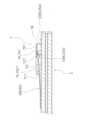
- FIG. FIG. 7 is a partially enlarged cross-sectional view taken along line VII in FIG. 6 (contacts are in a closed state).
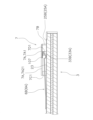
- FIG. 7 is a partially enlarged cross-sectional view taken along line VII in FIG. 6 (contacts are in an open state).
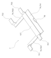
- FIG. 2 is an external perspective view of the shield plate as viewed from above.
- FIG. 4 is an external perspective view of the shield plate as viewed from below.
- 2 is a perspective view of the base assembly and the stand as viewed from below.
- FIG. FIG. 4 is a perspective view of the base assembly as viewed from below.
- FIG. 2 is a cross-sectional view of an electromagnetic relay in an open state.
- FIG. 2 is a cross-sectional view of an electromagnetic relay in a closed state.
- FIG. FIG. 11 is a partially enlarged cross-sectional view of a printed circuit board and a shield plate according to another embodiment.
- FIG. 11 is a partially enlarged cross-sectional view of a printed circuit board and a shield plate according to another embodiment.
- the electromagnetic relay according to this embodiment is used to switch between a high-frequency RF signal (an example of a high-frequency signal) and a low-frequency DC signal (an example of a low-frequency signal).
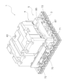
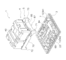
- FIGS. 1 and 2 are perspective views of an electromagnetic relay 1 according to an embodiment.
- the electromagnetic relay 1 comprises a case 2, a base block 3, a base assembly 4, and a stand 5. Note that the case 2 is omitted in FIG. 2.
- the direction in which the base assembly 4 and the stand 5 are arranged with respect to the printed circuit board 3 is defined as the upper side, and the opposite direction is defined as the lower side.
- FIG. 3 is an exploded perspective view of the electromagnetic relay 1.
- the electromagnetic relay 1 includes a first movable contact piece 6A (an example of a movable contact piece), a second movable contact piece 6B (an example of a movable contact piece), and a shield plate 7. The first movable contact piece 6A, the second movable contact piece 6B, and the shield plate 7 are arranged on the printed circuit board 3.
- FIG. 4 is a perspective view of the printed circuit board 3. Note that the shield plate 7 is omitted in FIG. 4.
- the printed circuit board 3 includes first to fourth conductor layers 11-14 and first to third dielectric layers 15-17.
- the first to fourth conductor layers 11-14 are made of an electrically conductive material such as copper.
- the first to third dielectric layers 15-17 are made of a dielectric material.
- the first to fourth conductor layers 11-14 and the first to third dielectric layers 15-17 are stacked alternately with each other.
- the first conductor layer 11 is provided on the upper surface of the printed circuit board 3.
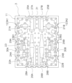
- FIG. 5 is a top view of the printed circuit board 3. Note that the shield plate 7 and the first and second movable contact pieces 6A, 6B are omitted in FIG. 5.
- the first conductor layer 11 is provided with a first RF line 21A, a second RF line 21B, a first DC line 22A, a second DC line 22B, a first ground plate 23 (an example of a ground plate), and a pair of second ground plates 123A1, 123A2 (an example of a ground plate).
- the first RF line 21A and the second RF line 21B are transmission lines for passing an RF signal.
- the first RF line 21A includes a first transmission line 24A (an example of a first transmission line) and a second transmission line 25A (an example of a second transmission line).
- the first transmission line 24A and the second transmission line 25A are arranged apart from each other.
- the first transmission line 24A and the second transmission line 25A are electrically isolated from each other.
- the first transmission line 24A is connected to a first input terminal 26A.
- the second transmission line 25A is connected to a first RF terminal 27A.
- the first input terminal 26A and the first RF terminal 27A are through-hole terminals provided on the end faces of the printed circuit board 3.
- the second RF line 21B includes a third transmission line 24B (an example of a first transmission line) and a fourth transmission line 25B (an example of a second transmission line).
- the third transmission line 24B and the fourth transmission line 25B are arranged apart from each other.
- the third transmission line 24B and the fourth transmission line 25B are electrically isolated from each other.
- the third transmission line 24B is connected to a second input terminal 26B.
- the fourth transmission line 25B is connected to a second RF terminal 27B.
- the second input terminal 26B and the second RF terminal 27B are each a through-hole terminal provided on an end surface of the printed circuit board 3.
- the first DC line 22A and the second DC line 22B are transmission lines for passing DC signals.
- the first DC line 22A is connected to the first transmission line 24A and the first ground plate 23.
- a first inductor 28A and a first capacitor 29A are arranged on the first DC line 22A. Note that in the drawings, only a portion of the first inductor 28A is labeled with the reference symbol 28A, and the reference symbols for the other first inductors 28A are omitted.
- the first DC line 22A is connected to the first DC terminal 30A between the first inductor 28A and the first capacitor 29A.
- the first DC terminal 30A is a through-hole terminal provided on the end surface of the printed circuit board 3.
- the first DC line 22A, the first inductor 28A, and the first capacitor 29A function as a low-pass filter that passes DC signals but cuts RF signals.
- the first inductor 28A and the first capacitor 29A are set to cut high-frequency signals of, for example, 1 kHz or higher.
- the second DC line 22B is connected to the third transmission line 24B and the first ground plate 23.
- a second inductor 28B and a second capacitor 29B are arranged on the second DC line 22B. Note that in the drawing, only a portion of the second inductor 28B is labeled with the reference symbol 28B, and the reference symbols for the other second inductors 28B are omitted.
- the second DC line 22B is connected to the second DC terminal 30B between the second inductor 28B and the second capacitor 29B.
- the second DC terminal 30B is a through-hole terminal provided on the end surface of the printed circuit board 3.
- the second DC line 22B, the second inductor 28B, and the second capacitor 29B function as a low-pass filter that passes DC signals but cuts RF signals.
- the second inductor 28B and the second capacitor 29B are set to cut high-frequency signals of, for example, 1 kHz or higher.
- the first ground plate 23 has a ground line 23A and a pair of ground portions 23B1, 23B2.
- the ground line 23A extends between the first transmission line 24A and the third transmission line 24B, along the first transmission line 24A and the third transmission line 24B.
- the ground line 23A extends between the second transmission line 25A and the fourth transmission line 25B, along the second transmission line 25A and the fourth transmission line 25B.
- the pair of ground parts 23B1, 23B2 are formed integrally with the ground line 23A.
- the pair of ground parts 23B1, 23B2 are arranged on both sides of the ground line 23A.
- the pair of ground parts 23B1, 23B2 are arranged on both sides of the first movable contact piece 6A and the second movable contact piece 6B when viewed from above the printed circuit board 3.
- the pair of second ground plates 123A1, 123A2 are each formed separately from the first ground plate 23.
- the pair of second ground plates 123A1, 123A2 may be formed integrally with the first ground plate 23.
- the pair of second ground plates 123A1, 123A2 are arranged on both sides of the second transmission line 25A and the fourth transmission line 25B.
- the second transmission line 25A is arranged between the ground line 23A and the second ground plate 123A1.
- the fourth transmission line 25B is arranged between the ground line 23A and the second ground plate 123A2.
- the pair of second ground plates 123A1, 123A2 are arranged on both sides of the first movable contact piece 6A and the second movable contact piece 6B when viewed from above the printed circuit board 3.
- the second to fourth conductor layers 12-14 shown in FIG. 4 are ground layers.
- a plurality of through-hole terminals 31 are provided on the end face of the printed circuit board 3. Note that in the drawings, only some of the through-hole terminals 31 are labeled with the reference numeral 31, and the reference numerals of the other through-hole terminals 31 are omitted.
- the through-hole terminals 31 connect the first ground plate 23 and the second to fourth conductor layers 12-14 described above.
- the first movable contact piece 6A and the second movable contact piece 6B are arranged on the printed circuit board 3.
- the first movable contact piece 6A is arranged above the first RF line 21A.
- the first movable contact piece 6A extends from the first transmission line 24A toward the second transmission line 25A.
- the first movable contact piece 6A includes a first connection portion 32A, a first contact portion 33A, and a first intermediate portion 34A.
- the first connection portion 32A is connected to the first transmission line 24A.
- the first contact portion 33A is arranged above the second transmission line 25A.
- the first intermediate portion 34A is located between the first connection portion 32A and the first contact portion 33A.
- the first movable contact piece 6A can move between a connected position and a disconnected position (an example of a disconnected position).
- a disconnected position an example of a disconnected position.
- the first contact portion 33A contacts the second transmission line 25A.
- the first movable contact piece 6A connects the first transmission line 24A and the second transmission line 25A.
- the first contact portion 33A is separated from the second transmission line 25A.
- the first movable contact piece 6A disconnects the first transmission line 24A from the second transmission line 25A.
- the first movable contact piece 6A contacts the shield plate 7 in the disconnecting position via the insulating layer 107, which will be described later.
- the second movable contact piece 6B is disposed above the second RF line 21B.
- the second movable contact piece 6B extends from the third transmission line 24B toward the fourth transmission line 25B.
- the second movable contact piece 6B includes a second connection portion 32B, a second contact portion 33B, and a second intermediate portion 34B.
- the second connection portion 32B is connected to the third transmission line 24B.
- the second contact portion 33B is disposed above the fourth transmission line 25B.
- the second intermediate portion 34B is located between the second connection portion 32B and the second contact portion 33B.
- the second movable contact piece 6B can move between a connection position and a disconnection position.
- the second contact portion 33B contacts the fourth transmission line 25B.
- the second movable contact piece 6B connects the third transmission line 24B and the fourth transmission line 25B.
- the second contact portion 33B disengages from the fourth transmission line 25B.
- the second movable contact piece 6B disconnects the third transmission line 24B and the fourth transmission line 25B.
- the second movable contact piece 6B contacts the shield plate 7 via the insulating layer 107 described below in the disconnection position.
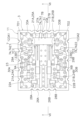
- the shield plate 7 is disposed on the printed circuit board 3. As shown in FIG. 3 and FIG. 6, the shield plate 7 is connected to the first ground plate 23. In detail, the shield plate 7 is connected to the first ground plate 23 and the pair of second ground plates 123A1, 123A2.
- the shield plate 7 is made of a conductive material.
- the shield plate 7 extends from the first ground plate 23 above the second transmission line 25A and above the fourth transmission line 25B. As shown in FIGS. 7A and 7B, the shield plate 7 is disposed above the first contact portion 33A and the second contact portion 33B. That is, the first contact portion 33A is disposed between the shield plate 7 and the second transmission line 25A. The second contact portion 33B is disposed between the shield plate 7 and the fourth transmission line 25B. The shield plate 7 improves the isolation characteristics between the first RF line 21A and the second RF line 21B.
- the shield plate 7 has a shield portion 7A, a first leg portion 7B, a pair of second legs 7C1, 7C2, and a pair of third legs 7D1, 7D2.
- the shield portion 7A has a shield body 7A1 and a pair of connecting portions 7A21, 7A22.
- the shield body 7A1 is formed in a rectangular plate shape.
- the shield body 7A1 is disposed above the second transmission line 25A and the fourth transmission line 25B at a distance from the second transmission line 25A and the fourth transmission line 25B.
- the pair of connecting portions 7A21, 7A22 each protrude from the shield body 7A1.
- the pair of connecting portions 7A21, 7A22 are arranged at a distance from each other.
- the pair of connecting portions 7A21, 7A22 are arranged on both sides of the first movable contact piece 6A and the second movable contact piece 6B when viewed from above the printed circuit board 3.
- the first leg 7B is formed integrally with the shield body 7A1 of the shield part 7A. As shown in FIG. 6, the first leg 7B extends from the shield body 7A1 toward the ground line 23A. The first leg 7B is disposed on the ground line 23A.
- each of the pair of second legs 7C1, 7C2 is formed integrally with each of the pair of connecting portions 7A21, 7A22 of the shield portion 7A. As shown in FIG. 6, each of the pair of second legs 7C1, 7C2 extends from each of the pair of connecting portions 7A21, 7A22 toward each of the pair of ground portions 23B1, 23B2.
- the pair of third legs 7D1, 7D2 are formed integrally with the shield body 7A1 of the shield part 7A. As shown in FIG. 6, the pair of third legs 7D1, 7D2 extend separately from the shield body 7A1 toward the pair of second ground plates 123A1, 123A2. The pair of third legs 7D1, 7D2 are disposed separately on the pair of second ground plates 123A1, 123A2.
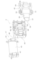
- Figure 9 is a perspective view of the base assembly 4 and the stand 5 as viewed from below.
- Figure 10 is a perspective view of the base assembly 4 as viewed from below.
- Figure 11 is an exploded perspective view of the base assembly 4.
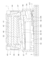
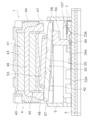
- Figures 12A and 12B are cross-sectional views of the electromagnetic relay 1. As shown in Figures 9 to 12B, the base assembly 4 includes a base 40, a coil block 41, and a movable block 42.
- the coil block 41 includes a coil 43, a spool 44, and an iron core 45.
- the coil 43 is wound around the spool 44.
- the iron core 45 is disposed within the coil 43.
- the iron core 45 includes an intermediate portion 46, a first suction portion 47, and a second suction portion 48.
- the intermediate portion 46 is disposed within the coil 43 and extends in the axial direction of the coil 43.
- the first suction portion 47 protrudes from the coil 43 in the axial direction of the coil 43.
- the first suction portion 47 is disposed facing downward.
- the second suction portion 48 protrudes from the coil 43 in the opposite direction to the first suction portion 47 in the axial direction of the coil 43.
- the second suction portion 48 is disposed facing downward.
- the second hinge spring 52 is disposed in the second support recess 63.
- the second hinge spring 52 is connected to the base 40 at the second support recess 63.
- the movable insulating base 55 is supported on the base 40 so as to be swingable around the first hinge spring 51 and the second hinge spring 52.
- FIG. 12A shows the electromagnetic relay 1 in an open state.
- the coil 43 is not excited, and the iron piece 50 is not attracted to the iron core 45.
- the first end 56 of the iron piece 50 is attracted to the first attraction portion 47 of the iron core 45 by the magnetic force of the permanent magnet 53 and is in contact with the first attraction portion 47. Therefore, the card 54 is separated from the first movable contact piece 6A and the second movable contact piece 6B, and the first movable contact piece 6A and the second movable contact piece 6B are each located in the disconnection position. Therefore, in the first RF line 21A, the first transmission line 24A and the second transmission line 25A are disconnected from each other. Also, in the second RF line 21B, the third transmission line 24B and the fourth transmission line 25B are disconnected from each other.
- the electromagnetic relay 1 when an RF signal is input to the first input terminal 26A and the second input terminal 26B of the electromagnetic relay 1, the electromagnetic relay 1 is closed.
- the first transmission line 24A and the second transmission line 25A are connected to each other, and the third transmission line 24B and the fourth transmission line 25B are connected to each other. Therefore, the RF signal is output from the first input terminal 26A through the first RF line 21A to the first RF terminal 27A.
- the RF signal is output from the second input terminal 26B through the second RF line 21B to the second RF terminal 27B. Meanwhile, the RF signal is cut at the first DC line 22A and the second DC line 22B, respectively, and therefore the RF signal is prevented from being output from the first and second DC terminals 30A and 30B.
- the insulating layer 107 is attached to the shield plate 7 as a separate member from the first and second movable contact pieces 6A, 6B and the shield plate 7. This allows the insulating layer 107 to be easily attached to the shield plate 7.
- an appropriate material can be selected from the various materials that can be used as the insulating layer 107.
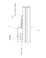
- the insulating layer 207 may be disposed separately between the first ground plate 23 and the shield plate 7, and between the second ground plates 123A1, 123A2 and the shield plate 7.
- FIG. 14 is a cross-sectional view of the printed circuit board 3 cut in a direction perpendicular to the longitudinal direction of the first movable contact piece 6A. The reference numerals for the cross section on the second movable contact piece 6B side are shown in parentheses. Even with this configuration, the insulating layer 207 can prevent a short circuit of low-frequency signals when the first movable contact piece 6A and the second movable contact piece 6B come into contact with the shield plate 7.
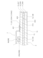
- the electromagnetic relay 1 may have a first insulating layer 307, a second insulating layer 308, a third insulating layer 309, and a fourth insulating layer 310.
- FIG. 15 is a cross-sectional view of the printed circuit board 3 cut in a direction perpendicular to the longitudinal direction of the first movable contact piece 6A. The reference numerals for the cross section on the second movable contact piece 6B side are shown in parentheses. In FIG. 15, vias 401, 402, and 403, which will be described later, are shown in a simplified form.
- the first dielectric layer 15 is used as the first insulating layer 307.
- the second dielectric layer 16 is used as the second insulating layer 308.
- the third dielectric layer 17 is used as the third insulating layer 309.
- the second conductor layer 12 has a fifth conductor layer 12A connected to the shield plate 7, and a sixth conductor layer 12B connected to the fourth conductor layer 14.
- the fifth conductor layer 12A is connected to the first ground plate 23 and the pair of second ground plates 123A1, 123A2 of the first conductor layer 11 through vias 401.
- the shield plate 7 is connected to the first ground plate 23 and the pair of second ground plates 123A1, 123A2.
- the sixth conductor layer 12B is a separate conductor layer from the fifth conductor layer 12A.
- the sixth conductor layer 12B is arranged around the fifth conductor layer 12A at a distance.
- the sixth conductor layer 12B is connected to the third conductor layer 13 via a via 402.
- the third conductor layer 13 is connected to the fourth conductor layer 14 via a via 403.
- the fourth insulating layer 310 is disposed between the fifth conductor layer 12A and the sixth conductor layer 12B, between the first insulating layer 307 and the second insulating layer 308.
- the fourth insulating layer 310 is disposed between the fifth conductor layer 12A and the sixth conductor layer 12B so as to surround the fifth conductor layer 12A.
- the fifth conductor layer 12A and the sixth conductor layer 12B are insulated by the fourth insulating layer 310.
- at least one of the sixth conductor layer 12B, the third conductor layer 13, and the fourth conductor layer 14 is interpreted as an example of a ground plate.
- the first to fourth insulating layers 307, 308, 309, and 310 can prevent a short circuit of the low-frequency signal.
- the fifth conductor layer 12A can ensure a large conductor area, improving the isolation characteristics of high-frequency signals.
- the configuration of the printed circuit board 3 is not limited to that of the above embodiment and may be modified.
- the configuration of the transmission lines of the printed circuit board 3 is not limited to that of the above embodiment and may be modified.
- the second RF line 21B and the second DC line 22B may be omitted.
- the configuration of the terminals of the printed circuit board 3 is not limited to that of the above embodiment and may be modified.
- the second input terminal 26B, the second RF terminal 27B, and the second DC terminal 30B may be omitted.
- the RF signal and the DC signal may be passed in the opposite direction to that of the above embodiment.
- the configuration of the base assembly 4 is not limited to that of the above embodiment and may be modified.
- the stand 5 is not limited to being separate from the base 40 and may be integrated with it.
- the electromagnetic relay of the present invention can stably transmit high-frequency and low-frequency signals without degrading the isolation characteristics.
Landscapes
- Physics & Mathematics (AREA)
- Electromagnetism (AREA)
- Waveguide Switches, Polarizers, And Phase Shifters (AREA)
Abstract
電磁継電器(1)では、プリント基板(3)は、第1及び第3伝送線路(24A,24B)と、第2及び第4伝送線路(25A,25B)と、第1グランド板(23)と、を有する。第1及び第2可動接触片(6A,6B)は、第1伝送線路(24A)及び第3伝送線路(24B)に各別に接続される。第1及び第2可動接触片(6A,6B)は接続位置と遮断位置との間で移動する。シールド板(7)は、第1グランド板(23)から第2及び第4伝送線路(25A,25B)の上方に延びる。絶縁層(107)は、第1グランド板(23)及び第1及び第2可動接触片(6A,6B)の間に設けられる。
Description
本発明は、電磁継電器に関する。
電磁継電器には、高周波信号の伝送を開閉するためのものがある。例えば、特許文献1の電磁継電器は、可動接触片と、複数の固定端子と、シールド板と、を備えている。可動接触片が電磁石ブロックによって押圧された場合、可動接触片の両端部が複数の固定端子に接触する。これにより、高周波信号の伝送が許可される。一方で、可動接触片が復帰バネによって付勢された場合、可動接触片の両端部は、複数の固定端子から離脱し、シールド板に接触する。これにより、高周波信号の伝送が遮断される。
従来の電磁継電器では、可動接触片の両端部を固定端子に接触させたり、可動接触片の両端部を固定端子から離脱させたりすることによって、高周波信号の伝送が開閉される。
この場合、可動接触片の全体を固定端子に接近させたり、可動接触片の全体を固定端子から離脱させたりする必要がある。この構成を実現するためには、電磁継電器の構成が複雑になるという問題がある。また、可動接触片を全体的に可動させるためには、電磁石ブロックの押圧力、すなわち、電磁石のパワーが要求されるという問題もある。
この問題を解決するために、可動接触片が全体的に可動するのではなく可動接触片が部分的に可動する電磁継電器の開発が、試みられている。このタイプの電磁継電器は、以下のように構成されうる。可動接触片の一端が第1伝送線路の固定端子に接続される。この状態で、可動接触片が押圧部材によって押圧され、可動接触片の他端が第2伝送線路の固定端子に接触する。これにより、高周波信号の伝送が許可される。
この状態で、可動接触片に対する押圧部材の押圧が解除されると、可動接触片の他端が第2伝送線路の固定端子から離脱しシールド板に接触する。これにより、高周波信号の伝送が遮断される。
一方で、高周波信号の伝送だけでなく低周波信号も伝送することができる電磁継電器の開発も、同時に試みられている。この場合、高周波信号の伝送が遮断され可動接触片の他端がシールド板に接触した状態で低周波信号が伝送されると、低周波信号が短絡するおそれがある。この問題を解決するために、この電磁継電器からシールド板が取り除かれた場合、低周波信号の短絡を防ぐことはできるものの、高周波信号のアイソレーション特性が低下するおそれがある。
本発明の目的は、高周波信号のアイソレーション特性を低下させることなく、高周波信号及び低周波信号を安定的に伝送することができる電磁継電器を、提供することにある。
本発明の一態様に係る電磁継電器は、ベースブロックと、可動接触片と、シールド板と、絶縁層と、を備える。ベースブロックは、第1伝送線路、第2伝送線路、及びグランド板を含む。可動接触片は、第1伝送線路に接続される。可動接触片は、第1伝送線路から第2伝送線路に向けて延びる。可動接触片は、第2伝送線路に接続される接続位置と、第2伝送線路から上方に離れた離脱位置との間で、移動する。シールド板は、グランド板に配置される。シールド板は、グランド板から第2伝送線路の上方に延びる。絶縁層は、グランド板及び可動接触片の間に設けられる。可動接触片が離脱位置に位置する状態で、可動接触片は絶縁層又はシールド板に接触する。
本態様に係る電磁継電器では、絶縁層がグランド板及び可動接触片の間に設けられる。可動接触片は、第1伝送線路に接続された状態で、第2伝送線路に接続される。これにより、高周波信号の伝送が許可される。この状態で、可動接触片が接続位置から離脱位置に移動した場合、可動接触片が絶縁層又はシールド板に接触する。これにより、高周波信号の伝送が遮断される。この際に、低周波信号が伝送されたとしても、絶縁層によって低周波信号の短絡を防ぐことができる。このように、本電磁継電器では、高周波信号のアイソレーション特性を低下させることなく、高周波信号及び低周波信号を安定的に伝送することができる。
絶縁層は、可動接触片及びシールド板とは別部材として、可動接触片及びシールド板のいずれか一方に装着されてもよい。この場合、絶縁層を可動接触片及びシールド板のいずれか一方に容易に装着することができる。また、絶縁層として用いられる様々な材料の中から、適切な材料を選択することができる。
絶縁層は、可動接触片及びシールド板のいずれか一方をコーティングすることによって、可動接触片及びシールド板のいずれか一方に形成されてもよい。この場合、絶縁層を可動接触片及びシールド板のいずれか一方に安定的に形成することができる。また、組立工数を低減することができる。
絶縁層は、グランド板及びシールド板の間に配置されてもよい。このように構成しても、可動接触片がシールド板に接触した場合に、絶縁層によって低周波信号の短絡を防ぐことができる。
電磁継電器は、導体をさらに備えていてもよい。この場合、導体は、シールド板に接続される。導体は、シールド板及びグランド板の間に配置される。絶縁層は、導体及びグランド板の間に配置される。このように構成しても、可動接触片がシールド板に接触した場合に、絶縁層によって低周波信号の短絡を防ぐことができる。
ベースブロックは、グランド板と、シールド板及びグランド板の間に配置される複数の導体層と、を含んでいてもよい。この場合、絶縁層は、複数の導体層のいずれか1つに設けられる。このように構成しても、可動接触片がシールド板に接触した場合に、絶縁層によって低周波信号の短絡を防ぐことができる。また、導体層によって導体の面積を大きく確保することができるので、高周波信号のアイソレーション特性を向上することができる。
絶縁層は、3μm以上且つ80μm以下の厚みを有していてもよい。絶縁層は、高誘電材料及び高誘電正接材料の少なくともいずれか一方によって、形成されてもよい。この構成によって、高周波信号のアイソレーション特性を向上することができる。
本発明の電磁継電器では、高周波信号のアイソレーション特性を低下させることなく、高周波信号及び低周波信号を安定的に伝送することができる。
以下、図面を参照して実施形態にかかる電磁継電器について説明する。本実施形態に係る電磁継電器は、高周波のRF信号(高周波信号の一例)と低周波のDC信号(低周波信号の一例)とを切り替えるために用いられる。
図1及び図2は、実施形態に係る電磁継電器1の斜視図である。図1及び図2に示すように、電磁継電器1は、ケース2と、ベースブロック3と、ベースアッシー4と、スタンド5とを備える。なお、図2では、ケース2は省略されている。以下の説明では、プリント基板3に対して、ベースアッシー4とスタンド5とが配置されている方向が上方、その反対の方向が下方と定義される。
図1に示すように、ケース2は、ベースブロック3に取り付けられている。ケース2は、ベースブロック3の上面と、ベースアッシー4と、スタンド5とを覆う。ベースブロック3は、プリント基板、セラミック基板、樹脂成型品、金属成型品、フレキシブル基板、及びMID(Molded Interconnect Device)を含む。本実施形態では、ベースブロック3がプリント基板である場合の例が示される。以下では、ベースブロックが”プリント基板3”という文言を用いて説明される。図3は、電磁継電器1の分解斜視図である。図3に示すように、電磁継電器1は、第1可動接触片6A(可動接触片の一例)と、第2可動接触片6B(可動接触片の一例)と、シールド板7とを備える。第1可動接触片6Aと、第2可動接触片6Bと、シールド板7とは、プリント基板3上に配置されている。
図4は、プリント基板3の斜視図である。なお、図4では、シールド板7は省略されている。図4に示すように、プリント基板3は、第1~第4導体層11-14と、第1~第3誘電体層15-17とを含む。第1~第4導体層11-14は、銅などの電気伝導性を有する材料製である。第1~第3誘電体層15-17は、誘電体製である。第1~第4導体層11-14と第1~第3誘電体層15-17とは、互いに交互に積層されている。
第1導体層11は、プリント基板3の上面に設けられている。図5は、プリント基板3の上面図である。なお、図5では、シールド板7と第1及び第2可動接触片6A,6Bとは省略されている。図4及び図5に示すように、第1導体層11には、第1RF線路21Aと、第2RF線路21Bと、第1DC線路22Aと、第2DC線路22Bと、第1グランド板23(グランド板の一例)と、1対の第2グランド板123A1,123A2(グランド板の一例)と、が設けられている。
第1RF線路21Aと第2RF線路21Bとは、RF信号を通すための伝送路である。第1RF線路21Aは、第1伝送線路24A(第1伝送線路の一例)と第2伝送線路25A(第2伝送線路の一例)とを含む。第1伝送線路24Aと第2伝送線路25Aとは、互いに離れて配置されている。第1伝送線路24Aと第2伝送線路25Aとは、電気的に互いに遮断されている。第1伝送線路24Aは、第1入力端子26Aに接続されている。第2伝送線路25Aは、第1RF端子27Aに接続されている。第1入力端子26Aと第1RF端子27Aとは、それぞれプリント基板3の端面に設けられたスルーホール端子である。
第2RF線路21Bは、第3伝送線路24B(第1伝送線路の一例)と第4伝送線路25B(第2伝送線路の一例)とを含む。第3伝送線路24Bと第4伝送線路25Bとは、互いに離れて配置されている。第3伝送線路24Bと第4伝送線路25Bとは、電気的に互いに遮断されている。第3伝送線路24Bは、第2入力端子26Bに接続されている。第4伝送線路25Bは、第2RF端子27Bに接続されている。第2入力端子26Bと第2RF端子27Bとは、それぞれプリント基板3の端面に設けられたスルーホール端子である。
第1DC線路22Aと第2DC線路22Bとは、DC信号を通すための伝送路である。第1DC線路22Aは、第1伝送線路24Aと第1グランド板23とに接続されている。第1DC線路22A上には、第1インダクタ28Aと第1キャパシタ29Aとが配置されている。なお、図面においては、第1インダクタ28Aの一部のみに符号28Aが付されており、他の第1インダクタ28Aの符号は省略されている。
第1DC線路22Aは、第1インダクタ28Aと第1キャパシタ29Aとの間において、第1DC端子30Aに接続されている。第1DC端子30Aは、プリント基板3の端面に設けられたスルーホール端子である。第1DC線路22Aと第1インダクタ28Aと第1キャパシタ29Aとは、DC信号を通過させるが、RF信号をカットするローパスフィルターとして機能する。第1インダクタ28Aと第1キャパシタ29Aとは、例えば1kHz以上の高周波信号をカットするように設定されている。
第2DC線路22Bは、第3伝送線路24Bと第1グランド板23とに接続されている。第2DC線路22B上には、第2インダクタ28Bと第2キャパシタ29Bとが配置されている。なお、図面においては、第2インダクタ28Bの一部のみに符号28Bが付されており、他の第2インダクタ28Bの符号は省略されている。
第2DC線路22Bは、第2インダクタ28Bと第2キャパシタ29Bとの間において、第2DC端子30Bに接続されている。第2DC端子30Bは、プリント基板3の端面に設けられたスルーホール端子である。第2DC線路22Bと第2インダクタ28Bと第2キャパシタ29Bとは、DC信号を通過させるが、RF信号をカットするローパスフィルターとして機能する。第2インダクタ28Bと第2キャパシタ29Bとは、例えば1kHz以上の高周波信号をカットするように設定されている。
図4、図5、及び図6に示すように、第1グランド板23は、グランド線路23Aと、1対のグランド部23B1,23B2と、を有する。グランド線路23Aは、第1伝送線路24A及び第3伝送線路24Bの間において、第1伝送線路24A及び第3伝送線路24Bに沿って延びる。グランド線路23Aは、第2伝送線路25A及び第4伝送線路25Bの間において、第2伝送線路25A及び第4伝送線路25Bに沿って延びる。
1対のグランド部23B1,23B2は、グランド線路23Aと一体に形成される。1対のグランド部23B1,23B2は、グランド線路23Aの両側に配置される。1対のグランド部23B1,23B2は、プリント基板3の上方視において、第1可動接触片6A及び第2可動接触片6Bの両側に配置される。
1対の第2グランド板123A1,123A2のぞれぞれは、第1グランド板23とは別体に形成される。1対の第2グランド板123A1,123A2は、第1グランド板23と一体に形成されてもよい。1対の第2グランド板123A1,123A2は、第2伝送線路25A及び第4伝送線路25Bの両側に配置される。言い換えると、第2伝送線路25Aは、グランド線路23A及び第2グランド板123A1の間に、配置される。第4伝送線路25Bは、グランド線路23A及び第2グランド板123A2の間に、配置される。1対の第2グランド板123A1,123A2は、プリント基板3の上方視において、第1可動接触片6A及び第2可動接触片6Bの両側に配置される。
図4に示す第2~第4導体層12-14は、グランド層である。図4及び図5に示すように、プリント基板3の端面には、複数のスルーホール端子31が設けられている。なお、図面においては、スルーホール端子31の一部のみに符号31が付されており、他のスルーホール端子31の符号は省略されている。スルーホール端子31は、上述した第1グランド板23と第2~第4導体層12-14とを接続する。
図4に示すように、第1可動接触片6Aと第2可動接触片6Bとは、プリント基板3上に配置されている。第1可動接触片6Aは、第1RF線路21Aの上方に配置されている。第1可動接触片6Aは、第1伝送線路24Aから第2伝送線路25Aに向けて延びている。第1可動接触片6Aは、第1接続部32Aと、第1接点部33Aと、第1中間部34Aを含む。第1接続部32Aは、第1伝送線路24Aに接続されている。第1接点部33Aは、第2伝送線路25Aの上方に配置されている。第1中間部34Aは、第1接続部32Aと第1接点部33Aとの間に位置する。
後述するように、第1可動接触片6Aは、接続位置と遮断位置(離脱位置の一例)とに移動可能である。第1可動接触片6Aが接続位置で、第1接点部33Aは、第2伝送線路25Aに接触する。それにより、第1可動接触片6Aは、第1伝送線路24Aと第2伝送線路25Aとを接続する。
第1可動接触片6Aが遮断位置で、第1接点部33Aは、第2伝送線路25Aから離脱する。それにより、第1可動接触片6Aは、第1伝送線路24Aと第2伝送線路25Aとを遮断する。この状態において、第1可動接触片6Aは、遮断位置において、後述する絶縁層107を介してシールド板7に接触する。
第2可動接触片6Bは、第2RF線路21Bの上方に配置されている。第2可動接触片6Bは、第3伝送線路24Bから第4伝送線路25Bに向けて延びている。第2可動接触片6Bは、第2接続部32Bと、第2接点部33Bと、第2中間部34Bとを含む。第2接続部32Bは、第3伝送線路24Bに接続されている。第2接点部33Bは、第4伝送線路25Bの上方に配置されている。第2中間部34Bは、第2接続部32Bと第2接点部33Bとの間に位置する。
第1可動接触片6Aと同様に、第2可動接触片6Bは、接続位置と遮断位置とに移動可能である。第2可動接触片6Bが接続位置で、第2接点部33Bは、第4伝送線路25Bに接触する。それにより、第2可動接触片6Bは、第3伝送線路24Bと第4伝送線路25Bとを接続する。第2可動接触片6Bが遮断位置で、第2接点部33Bは、第4伝送線路25Bから離脱する。それにより、第2可動接触片6Bは、第3伝送線路24Bと第4伝送線路25Bとを遮断する。この状態において、第2可動接触片6Bは、遮断位置において、後述する絶縁層107を介してシールド板7に接触する。
図3に示すように、シールド板7は、プリント基板3上に配置されている。図3及び図6に示すように、シールド板7は、第1グランド板23に接続されている。詳細には、シールド板7は、第1グランド板23及び1対の第2グランド板123A1,123A2に接続されている。シールド板7は、導電性を有する材料で形成されている。
図6に示すように、シールド板7は、第1グランド板23から、第2伝送線路25Aの上方及び第4伝送線路25Bの上方に、延びている。図7A及び図7Bに示すように、シールド板7は、第1接点部33Aと第2接点部33Bとの上方に配置されている。すなわち、第1接点部33Aは、シールド板7及び第2伝送線路25Aの間に配置される。第2接点部33Bは、シールド板7及び第4伝送線路25Bの間に配置される。シールド板7により、第1RF線路21Aと第2RF線路21Bにおけるアイソレーション特性が向上する。
図8Aに示すように、シールド板7は、シールド部7Aと、第1脚部7Bと、1対の第2脚部7C1,7C2と、1対の第3脚部7D1,7D2と、を有する。シールド部7Aは、シールド本体7A1と、1対の連結部7A21,7A22と、を有する。シールド本体7A1は、矩形板状に形成される。
図6、図7A及び図7Bに示すように、シールド本体7A1は、第2伝送線路25A及び第4伝送線路25Bの上方において、第2伝送線路25A及び第4伝送線路25Bと間隔を隔てて配置される。
図8Aに示すように、1対の連結部7A21,7A22は、シールド本体7A1から各別に突出する。1対の連結部7A21,7A22は、互いに間隔を隔てて配置される。図6に示すように、1対の連結部7A21,7A22は、プリント基板3の上方視において、第1可動接触片6A及び第2可動接触片6Bの両側に配置される。
図8Aに示すように、第1脚部7Bは、シールド部7Aのシールド本体7A1と一体に形成される。図6に示すように、第1脚部7Bは、シールド本体7A1からグランド線路23Aに向けて延びる。第1脚部7Bは、グランド線路23Aに配置される。
図8Aに示すように、1対の第2脚部7C1,7C2のそれぞれは、シールド部7Aの1対の連結部7A21,7A22のそれぞれと一体に形成される。図6に示すように、1対の第2脚部7C1,7C2は、1対の連結部7A21,7A22から1対のグランド部23B1,23B2に向けて各別に延びる。
図8Aに示すように、1対の第3脚部7D1,7D2は、シールド部7Aのシールド本体7A1と一体に形成される。図6に示すように、1対の第3脚部7D1,7D2は、シールド本体7A1から1対の第2グランド板123A1,123A2に向けて各別に延びる。1対の第3脚部7D1,7D2は、1対の第2グランド板123A1,123A2に各別に配置される。
このように、シールド板7では、第1脚部7Bは第1グランド板23のグランド線路23Aに接続される。1対の第2脚部7C1,7C2は、第1グランド板23の1対のグランド部23B1,23B2に各別に接続される。1対の第3脚部7D1,7D2は、1対の第2グランド板123A1,123A2に各別に接続される。この状態において、シールド本体7A1には、図8Bに示す絶縁層107を介して、第1可動接触片6A及び第2可動接触片6Bが接触する。
図8Bに示すように、絶縁層107は、シールド板7に設けられる。図7Bに示すように、第1可動接触片6A及び第2可動接触片6Bが遮断位置に位置する状態で、絶縁層107には、第1可動接触片6Aの第1接点部33A及び第2可動接触片6Bの第2接点部33Bが、接触する。絶縁層107は、第1可動接触片6Aの第1接点部33A及び第2可動接触片6Bの第2接点部33Bのそれぞれに、設けられてもよい。この場合、第1可動接触片6A及び第2可動接触片6Bが遮断位置に位置する状態で、絶縁層107にはシールド板7が接触する。
絶縁層107は、第1可動接触片6A、第2可動接触片6B、及びシールド板7とは別部材である。絶縁層107は、接着剤によってシールド板7に貼り付けられる。絶縁層107は、3μm以上且つ80μm以下の厚みを有する。絶縁層107は、高誘電材料及び高誘電正接材料の少なくともいずれか一方によって、形成されることが好ましい。例えば、絶縁層107は、高誘電率を有する高誘電正接材料によって形成されることが好ましい。具体的には、絶縁層107は、セラミック、セラミック粒子を含む樹脂材料、フェライト、フェライト粒子を含む樹脂材料、及び電波吸収体のような材料によって、形成されることが好ましい。
絶縁層107は、シールド板7をコーティングすることによって、シールド板7に形成されてもよい。例えば、シールド板7において第1可動接触片6A及び第2可動接触片6Bに対向する部分には、フッ素コーティング及びポリアミドイミドコーティングが施される。これにより、シールド板7には、絶縁層107として機能する樹脂層が形成される。樹脂層は、3μm以上且つ80μm以下の厚みで形成されることが好ましい。
図9は、ベースアッシー4とスタンド5とを下方から見た斜視図である。図10は、ベースアッシー4を下方から見た斜視図である。図11は、ベースアッシー4の分解斜視図である。図12A及び図12Bは、電磁継電器1の断面図である。図9から図12Bに示すように、ベースアッシー4は、ベース40と、コイルブロック41と、可動ブロック42とを含む。
コイルブロック41は、コイル43と、スプール44と、鉄芯45とを含む。コイル43は、スプール44に巻回されている。鉄芯45は、コイル43内に配置される。鉄芯45は、中間部46と、第1吸引部47と、第2吸引部48とを含む。中間部46は、コイル43内に配置され、コイル43の軸線方向に延びている。第1吸引部47は、コイル43の軸線方向に、コイル43から突出している。第1吸引部47は、下方を向いて配置されている。第2吸引部48は、コイル43の軸線方向において、第1吸引部47と反対の方向に、コイル43から突出している。第2吸引部48は、下方を向いて配置されている。
可動ブロック42は、コイル43の電磁力によって動作することで、第1可動接触片6Aと第2可動接触片6Bとを接続位置と遮断位置との間で移動させる。図13は、可動ブロック42の斜視図である。図13に示すように、可動ブロック42は、鉄片50と、第1ヒンジバネ51と、第2ヒンジバネ52と、永久磁石53と、カード54と、可動絶縁台55と含む。
鉄片50は、可動絶縁台55に支持されている。鉄片50は、第1端部56と第2端部57とを含む。第1端部56は、コイル43の軸線方向に、可動絶縁台55から突出している。第1端部56は、鉄芯45の第1吸引部47の下方に配置されており、第1吸引部47に向かい合う。第2端部57は、コイル43の軸線方向において第1端部56と反対の方向に、可動絶縁台55から突出している。第2端部57は、鉄芯45の第2吸引部48の下方に配置されており、第2吸引部48に向かい合う。
第1ヒンジバネ51は、可動絶縁台55に支持されている。第1ヒンジバネ51は、可動絶縁台55の一側方に向かって、可動絶縁台55から突出している。第2ヒンジバネ52は、可動絶縁台55に支持されている。第2ヒンジバネ52は、可動絶縁台55の他側方に向かって、可動絶縁台55から突出している。永久磁石53は、可動絶縁台55の上面に取り付けられている。
カード54は、可動絶縁台55に支持されている。カード54は、可動絶縁台55から下方に突出している。カード54は、第1可動接触片6Aと第2可動接触片6Bとの上方に配置されている。詳細には、カード54は、第1可動接触片6Aの第1中間部34Aと、第2可動接触片6Bの第2中間部34Bとの上方に配置されている。カード54は、鉄片50の第1端部56の下面に接続されている。カード54は、第1端部56の下面から下方に突出している。
可動絶縁台55は、ベース40に対して揺動可能に支持されている。図11に示すように、ベース40は支持突起58,59を含む。図13に示すように、可動絶縁台55は、支持孔60,61を含む。支持突起58,59は、支持孔60,61内に配置され、可動絶縁台55を揺動可能に支持する。また、図11に示すように、ベース40は、第1支持凹部62と第2支持凹部63とを含む。第1ヒンジバネ51は、第1支持凹部62内に配置される。第1ヒンジバネ51は、第1支持凹部62においてベース40に接続される。第2ヒンジバネ52は、第2支持凹部63内に配置される。第2ヒンジバネ52は、第2支持凹部63においてベース40に接続される。可動絶縁台55は、第1ヒンジバネ51及び第2ヒンジバネ52回りに、揺動可能にベース40に支持される。
スタンド5は、プリント基板3の上方に配置され、ベースアッシー4を支持する。詳細には、スタンド5は、ベース40を支持する。コイルブロック41は、ベース40を介して、スタンド5に支持される。可動ブロック42は、ベース40を介して、スタンド5に支持される。スタンド5は、フレーム70と、複数の脚部71-74とを含む。図9に示すように、フレーム70には、中央部に開口75が設けられている。可動ブロック42は、フレーム70の開口75内に配置されている。カード54は、開口75を通って、下方に延びている。
次に、電磁継電器1の動作について説明する。図12Aは、開状態の電磁継電器1を示している。コイル43に電流が流されていない状態では、コイル43は励磁されておらず、鉄片50は鉄芯45に吸引されていない。永久磁石53に磁力により、鉄片50の第1端部56は、鉄芯45の第1吸引部47に吸引されて第1吸引部47に接触している。そのため、カード54は、第1可動接触片6A及び第2可動接触片6Bから離れており、第1可動接触片6Aと第2可動接触片6Bとは、それぞれ遮断位置に位置している。そのため、第1RF線路21Aにおいて、第1伝送線路24Aと第2伝送線路25Aとは互いに遮断されている。また、第2RF線路21Bにおいて、第3伝送線路24Bと第4伝送線路25Bとは互いに遮断されている。
コイル43に電流が流されている状態では、電磁継電器1は図12Bに示す閉状態となる。電磁継電器1が閉状態では、コイル43の電磁力により、鉄片50の第2端部57が、鉄芯45の第2吸引部48に吸引されて上昇する。それにより、鉄片50が揺動して、第1端部56が下降する。カード54は、第1端部56と共に下降して、第1可動接触片6Aと第2可動接触片6Bとを押圧することで、第1可動接触片6Aと第2可動接触片6Bとを、それぞれ接続位置に移動させる。それにより、第1RF線路21Aにおいて、第1伝送線路24Aと第2伝送線路25Aとは互いに接続される。また、第2RF線路21Bにおいて、第3伝送線路24Bと第4伝送線路25Bとは互いに接続される。
コイル43への電流が遮断されると、永久磁石53に磁力により、鉄片50が逆方向に回転し、第2端部57が下降して第2吸引部48から離れると共に、第1端部56が上昇する。カード54は、第1端部56と供に上昇して、第1可動接触片6Aと第2可動接触片6Bとから離れる。それにより、第1可動接触片6Aと第2可動接触片6Bとは、第1可動接触片6Aと第2可動接触片6Bとの弾性力により、それぞれ遮断位置に戻る。それにより、第1RF線路21Aにおいて、第1伝送線路24Aと第2伝送線路25Aとは互いに遮断される。また、第2RF線路21Bにおいて、第3伝送線路24Bと第4伝送線路25Bとは互いに遮断される。
例えば、電磁継電器1の第1入力端子26Aと第2入力端子26BとにRF信号が入力される場合には、電磁継電器1が閉状態とされる。この場合、第1伝送線路24Aと第2伝送線路25Aとは互いに接続され、第3伝送線路24Bと第4伝送線路25Bとは互いに接続されている。そのため、RF信号は、第1入力端子26Aから、第1RF線路21Aを通って、第1RF端子27Aから出力される。また、RF信号は、第2入力端子26Bから、第2RF線路21Bを通って、第2RF端子27Bから出力される。一方、RF信号は、第1DC線路22A、第2DC線路22Bにおいて、それぞれカットされるため、RF信号が第1、第2DC端子30A,30Bから出力されることが防止される。
電磁継電器1の第1入力端子26Aと第2入力端子26BとにDC信号が入力される場合には、電磁継電器1は開状態とされる。この場合、第1伝送線路24Aと第2伝送線路25Aとは互いに遮断され、第3伝送線路24Bと第4伝送線路25Bとは互いに遮断されている。そのため、DC信号は、第1入力端子26Aから、第1RF線路21Aを通らずに、第1DC線路22Aを通って、第1DC端子30Aから出力される。DC信号は、第2入力端子26Bから、第2RF線路21Bを通らずに、第2DC線路22Bを通って、第2DC端子30Bから出力される。それにより、DC信号が、第1可動接触片6Aと第2可動接触片6Bとに流れることが防止される。
以上説明した本実施形態に係る電磁継電器1では、絶縁層107が、第1グランド板23と、第1可動接触片6A及び第2可動接触片6Bとの間に、設けられる。詳細には、絶縁層107はシールド板7に設けられる。第1可動接触片6A及び第2可動接触片6Bは、第1伝送線路24A及び第3伝送線路24Bに各別に接続された状態で、第2伝送線路25A及び第4伝送線路25Bに各別に接続される。これにより、高周波信号の伝送が許可される。この状態で、第1及び第2可動接触片6A,6Bが接続位置から遮断位置に移動した場合、第1及び第2可動接触片6A,6Bは、シールド板7に装着された絶縁層107に、接触する。これにより、高周波信号の伝送が遮断される。この際に、DC信号が伝送されたとしても、絶縁層107によってDC信号の短絡を防ぐことができる。このように、本電磁継電器1では、RF信号のアイソレーション特性を低下させることなく、RF信号及びDC信号を安定的に伝送することができる。
絶縁層107は、第1及び第2可動接触片6A,6B及びシールド板7とは別部材として、シールド板7に装着される。これにより、絶縁層107をシールド板7に容易に装着することができる。また、絶縁層107として用いられる様々な材料の中から、適切な材料を選択することができる。
絶縁層107は、シールド板7をコーティングすることによって、シールド板7のいずれか一方に形成されてもよい。この場合、絶縁層107をシールド板7に安定的に形成することができる。また、組立工数を低減することができる。
絶縁層107は、3μm以上且つ80μm以下の厚みを有する。絶縁層107は、高誘電材料及び高誘電正接材料の少なくともいずれか一方によって、形成される。この構成によって、高周波信号のアイソレーション特性を向上することができる。
以上、本発明の一実施形態について説明したが、本発明は上記実施形態に限定されるものではなく、発明の要旨を逸脱しない範囲で種々の変更が可能である。
図14に示すように、絶縁層207は、第1グランド板23及びシールド板7の間と、第2グランド板123A1,123A2及びシールド板7の間とに、各別に配置されてもよい。なお、図14は、第1可動接触片6Aの長手方向に直交する方向にプリント基板3を切断した断面図である。第2可動接触片6B側の断面に関する符号は括弧内に示されている。このように構成しても、第1可動接触片6A及び第2可動接触片6Bがシールド板7に接触した場合に、絶縁層207によって低周波信号の短絡を防ぐことができる。
図15に示すように、電磁継電器1は、第1絶縁層307、第2絶縁層308、第3絶縁層309、及び第4絶縁層310を有していてもよい。なお、図15は、第1可動接触片6Aの長手方向に直交する方向にプリント基板3を切断した断面図である。第2可動接触片6B側の断面に関する符号は括弧内に示されている。図15では、後述するビア401,402,403は簡略化して示されている。
この場合、第1誘電体層15が第1絶縁層307として用いられる。第2誘電体層16は第2絶縁層308はとして用いられる。第3誘電体層17は第3絶縁層309として用いられる。
ここで、第2導体層12は、シールド板7に接続される第5導体層12Aと、第4導体層14に接続される第6導体層12Bと、を有する。第5導体層12Aは、ビア401を介して、第1導体層11の第1グランド板23及び1対の第2グランド板123A1,123A2に接続される。第1グランド板23及び1対の第2グランド板123A1,123A2には、シールド板7が接続される。
第6導体層12Bは、第5導体層12Aとは別体の導体層である。第6導体層12Bは、第5導体層12Aの周りに間隔を隔てて配置される。第6導体層12Bは、ビア402を介して、第3導体層13に接続される。第3導体層13は、ビア403を介して、第4導体層14に接続される。
第4絶縁層310は、第1絶縁層307及び第2絶縁層308の間において、第5導体層12A及び第6導体層12Bの間に配置される。例えば、第4絶縁層310は、第5導体層12Aを取り囲むように、第5導体層12A及び第6導体層12Bの間に配置される。これにより、第5導体層12A及び第6導体層12Bは、第4絶縁層310によって絶縁される。この場合、第6導体層12B、第3導体層13、及び第4導体層14の少なくともいずれか1つが、グランド板の一例として解釈される。
このように構成しても、第1可動接触片6A及び第2可動接触片6Bがシールド板7に接触した場合に、第1~第4絶縁層307,308,309,310によって低周波信号の短絡を防ぐことができる。また、この構成では、第5導体層12Aによって導体の面積を大きく確保することができるので、高周波信号のアイソレーション特性を向上することができる。
プリント基板3の構成は、上記の実施形態のものに限らず、変更されてもよい。プリント基板3の伝送線路の構成は、上記の実施形態のものに限らず、変更されてもよい。例えば、第2RF線路21Bと第2DC線路22Bとは、省略されてもよい。プリント基板3の端子の構成は、上記の実施形態のものに限らず、変更されてもよい。例えば、第2入力端子26Bと、第2RF端子27Bと、第2DC端子30Bとは、省略されてもよい。RF信号及びDC信号は、前記実施形態とは逆方向に流されてもよい。ベースアッシー4の構成は、上記の実施形態のものに限らず、変更されてもよい。例えば、スタンド5は、ベース40と別体に限らず、一体であってもよい。
本発明の電磁継電器では、アイソレーション特性を低下させることなく、高周波信号及び低周波信号を安定的に伝送することができる。
2:ケース、 3:プリント基板、 6A:第1可動接触片、6B:第2可動接触片、 7:シールド板、 7A:シールド部、 7B:第1脚部、 7C1,7C2:第2脚部、 7D1,7D2:第3脚部、 11:第1導体層、 12:第2導体層、 12A:第5導体層、 12B:第6導体層、 13:第3導体層、 14:第4導体層、 23:第1グランド板、 23A:グランド線路、 23B1,23B2:グランド部、 24A:第1伝送線路、 25A:第2伝送線路、 107,207,307,308,309,310:絶縁層、 123A1,123A2:第2グランド板
Claims (8)
- 第1伝送線路、第2伝送線路、及びグランド板を含むベースブロックと、
前記第1伝送線路に接続され、前記第1伝送線路から前記第2伝送線路に向けて延び、前記第2伝送線路に接続される接続位置と、前記第2伝送線路から上方に離れた離脱位置との間で移動する可動接触片と、
前記グランド板に配置され、前記グランド板から前記第2伝送線路の上方に延びるシールド板と、
前記グランド板及び前記可動接触片の間に設けられる絶縁層と、
を備え、
前記可動接触片が前記離脱位置に位置する状態で、前記可動接触片は前記絶縁層又は前記シールド板に接触する、
電磁継電器。
- 前記絶縁層は、前記可動接触片及び前記シールド板とは別部材として、前記可動接触片及び前記シールド板のいずれか一方に装着される、
請求項1に記載の電磁継電器。
- 前記絶縁層は、前記可動接触片及び前記シールド板の前記いずれか一方をコーティングすることによって、前記可動接触片及び前記シールド板のいずれか一方に形成される、
請求項1に記載の電磁継電器。
- 前記絶縁層は、前記グランド板及び前記シールド板の間に配置される、
請求項1に記載の電磁継電器。
- 前記シールド板に接続され前記グランド板及び前記シールド板の間に配置される導体、
をさらに備え、
前記絶縁層は、前記導体及び前記グランド板の間に配置される、
請求項4に記載の電磁継電器。
- 前記ベースブロックは、前記グランド板と、前記シールド板及び前記グランド板の間に配置される複数の導体層と、を含み、
前記絶縁層は、前記複数の導体層のいずれか1つに設けられる、
請求項4に記載の電磁継電器。
- 前記絶縁層は、3μm以上且つ80μm以下の厚みを有する、
請求項1から4のいずれか1項に記載の電磁継電器。
- 前記絶縁層は、高誘電材料及び高誘電正接材料の少なくともいずれか一方によって、形成される、
請求項1に記載の電磁継電器。
Applications Claiming Priority (2)
| Application Number | Priority Date | Filing Date | Title |
|---|---|---|---|
| JP2023153961A JP2025045911A (ja) | 2023-09-20 | 2023-09-20 | 電磁継電器 |
| JP2023-153961 | 2023-09-20 |
Publications (1)
| Publication Number | Publication Date |
|---|---|
| WO2025062897A1 true WO2025062897A1 (ja) | 2025-03-27 |
Family
ID=95072634
Family Applications (1)
| Application Number | Title | Priority Date | Filing Date |
|---|---|---|---|
| PCT/JP2024/029173 Ceased WO2025062897A1 (ja) | 2023-09-20 | 2024-08-16 | 電磁継電器 |
Country Status (3)
| Country | Link |
|---|---|
| JP (1) | JP2025045911A (ja) |
| TW (1) | TW202514689A (ja) |
| WO (1) | WO2025062897A1 (ja) |
Citations (4)
| Publication number | Priority date | Publication date | Assignee | Title |
|---|---|---|---|---|
| JPS5812220A (ja) * | 1981-07-15 | 1983-01-24 | 日本電気株式会社 | 高周波信号スイツチ |
| JP2001176347A (ja) * | 1999-12-22 | 2001-06-29 | Matsushita Electric Works Ltd | 高周波リレー及び高周波リレーの製造方法 |
| JP2003051234A (ja) * | 2001-05-30 | 2003-02-21 | Omron Corp | 電磁継電器 |
| JP2003346622A (ja) * | 2002-05-23 | 2003-12-05 | Omron Corp | 高周波リレー |
-
2023
- 2023-09-20 JP JP2023153961A patent/JP2025045911A/ja active Pending
-
2024
- 2024-08-16 WO PCT/JP2024/029173 patent/WO2025062897A1/ja not_active Ceased
- 2024-08-20 TW TW113131177A patent/TW202514689A/zh unknown
Patent Citations (4)
| Publication number | Priority date | Publication date | Assignee | Title |
|---|---|---|---|---|
| JPS5812220A (ja) * | 1981-07-15 | 1983-01-24 | 日本電気株式会社 | 高周波信号スイツチ |
| JP2001176347A (ja) * | 1999-12-22 | 2001-06-29 | Matsushita Electric Works Ltd | 高周波リレー及び高周波リレーの製造方法 |
| JP2003051234A (ja) * | 2001-05-30 | 2003-02-21 | Omron Corp | 電磁継電器 |
| JP2003346622A (ja) * | 2002-05-23 | 2003-12-05 | Omron Corp | 高周波リレー |
Also Published As
| Publication number | Publication date |
|---|---|
| TW202514689A (zh) | 2025-04-01 |
| JP2025045911A (ja) | 2025-04-02 |
Similar Documents
| Publication | Publication Date | Title |
|---|---|---|
| US9076615B2 (en) | Method of forming an integrated electromechanical relay | |
| EP1278223B1 (en) | High frequency relay | |
| JP4294590B2 (ja) | 電気機械マイクロスイッチ装置 | |
| US6100606A (en) | High frequency switching device | |
| US20020008596A1 (en) | Non-reciprocal circuit device and wireless communications equipment comprising same | |
| JP2025045911A (ja) | 電磁継電器 | |
| WO2025062899A1 (ja) | 電磁継電器 | |
| WO2025062898A1 (ja) | 電磁継電器 | |
| WO2025062914A1 (ja) | 電磁継電器 | |
| JP2025045917A (ja) | 電磁継電器 | |
| WO2025062916A1 (ja) | 電磁継電器 | |
| JP5158166B2 (ja) | 複合電子モジュール、この複合電子モジュールの製造方法 | |
| JP2025045919A (ja) | 電磁継電器 | |
| WO2025062917A1 (ja) | 回路部品 | |
| WO2025062911A1 (ja) | 電磁継電器 | |
| WO2025062913A1 (ja) | 電磁継電器 | |
| CN101233649A (zh) | 不可逆电路元件、复合电子零件及通信装置 | |
| JP4374544B2 (ja) | 2ポートアイソレータの特性調整方法 | |
| CN217280603U (zh) | 一种具有柔性连接带的射频开关 | |
| JP4097084B2 (ja) | 非可逆回路素子 | |
| US20050174187A1 (en) | Non-reciprocal circuit device including multilayer board |
Legal Events
| Date | Code | Title | Description |
|---|---|---|---|
| 121 | Ep: the epo has been informed by wipo that ep was designated in this application |
Ref document number: 24867978 Country of ref document: EP Kind code of ref document: A1 |
|
| NENP | Non-entry into the national phase |
Ref country code: DE |