WO2025057714A1 - 半導体チップ、通信方法、および通信システム - Google Patents
半導体チップ、通信方法、および通信システム Download PDFInfo
- Publication number
- WO2025057714A1 WO2025057714A1 PCT/JP2024/030366 JP2024030366W WO2025057714A1 WO 2025057714 A1 WO2025057714 A1 WO 2025057714A1 JP 2024030366 W JP2024030366 W JP 2024030366W WO 2025057714 A1 WO2025057714 A1 WO 2025057714A1
- Authority
- WO
- WIPO (PCT)
- Prior art keywords
- information
- host
- semiconductor chip
- signature
- image sensor
- Prior art date
- Legal status (The legal status is an assumption and is not a legal conclusion. Google has not performed a legal analysis and makes no representation as to the accuracy of the status listed.)
- Pending
Links
Images


Classifications
-
- G—PHYSICS
- G06—COMPUTING OR CALCULATING; COUNTING
- G06F—ELECTRIC DIGITAL DATA PROCESSING
- G06F21/00—Security arrangements for protecting computers, components thereof, programs or data against unauthorised activity
- G06F21/70—Protecting specific internal or peripheral components, in which the protection of a component leads to protection of the entire computer
- G06F21/71—Protecting specific internal or peripheral components, in which the protection of a component leads to protection of the entire computer to assure secure computing or processing of information
- G06F21/73—Protecting specific internal or peripheral components, in which the protection of a component leads to protection of the entire computer to assure secure computing or processing of information by creating or determining hardware identification, e.g. serial numbers
-
- H—ELECTRICITY
- H04—ELECTRIC COMMUNICATION TECHNIQUE
- H04L—TRANSMISSION OF DIGITAL INFORMATION, e.g. TELEGRAPHIC COMMUNICATION
- H04L9/00—Cryptographic mechanisms or cryptographic arrangements for secret or secure communications; Network security protocols
- H04L9/10—Cryptographic mechanisms or cryptographic arrangements for secret or secure communications; Network security protocols with particular housing, physical features or manual controls
Definitions
- This disclosure relates to a semiconductor chip, a communication method, and a communication system, and in particular to a semiconductor chip, a communication method, and a communication system that enable reliable management of the authenticity of the semiconductor chip.
- CMOS Complementary Metal-Oxide-Semiconductor
- Patent Document 1 technology has been proposed for achieving highly secure communication between an image sensor and a host (application processor).
- a semiconductor chip includes a communication interface that communicates with a host according to a specified communication standard, and a non-rewritable memory unit that stores ID information in a state that cannot be rewritten at the time of shipment, and outputs the ID information stored in the non-rewritable memory unit from the communication interface in response to a request from an external terminal via the host.
- a communication method includes a semiconductor chip having a communication interface for communicating with a host according to a predetermined communication standard and a non-rewritable memory unit that stores ID information in a state that cannot be rewritten at the time of shipment, and outputting the ID information stored in the non-rewritable memory unit from the communication interface in response to a request from an external terminal via the host.
- a communication system is a communication system that includes a semiconductor chip having a communication interface that communicates with a host according to a specified communication standard, a non-rewritable memory unit that stores ID information in a state that cannot be rewritten at the time of shipment, and an external terminal that transmits requests via the host, and outputs the ID information stored in the non-rewritable memory unit from the communication interface in response to the request.
- communication with the host is performed via a communication interface in accordance with a specified communication standard, and ID information is stored in a non-rewritable storage unit in a state in which it cannot be rewritten at the time of shipment. Then, in response to a request from an external terminal via the host, the ID information stored in the non-rewritable storage unit is output from the communication interface.
- FIG. 1 is a block diagram showing a configuration example of a first embodiment of a communication system to which the present technology is applied;
- FIG. 11 is a diagram showing an example of a product ID and a category ID.
- FIG. 2 is a diagram illustrating an IF function.
- 1 is a block diagram showing a configuration example of a second embodiment of a communication system to which the present technology is applied;
- FIG. 11 is a diagram illustrating an example of a first selection method for selecting ID information.
- FIG. 11 is a diagram illustrating an example of a second selection method for selecting ID information.
- FIG. 11 is a sequence diagram illustrating an example of a communication process.
- FIG. 13 is a block diagram showing a configuration example of a third embodiment of a communication system to which the present technology is applied.
- FIG. 11 is a diagram showing an example of a format of image data into which signature data is inserted;
- FIG. 11 is a diagram illustrating an example of use of ID information.
- 1 is a block diagram showing an example of the configuration of an embodiment of a computer to which the present technology is applied.
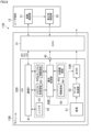
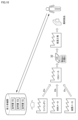
- FIG. 1 is a block diagram showing a configuration example of a first embodiment of a communication system to which the present technology is applied.
- the communication system 11 shown in FIG. 1 can manage the authenticity of the CMOS image sensor 32 mounted on the module 13 by having the user terminal 12 communicate with the module 13.
- the user terminal 12 is configured with a startup confirmation unit 21 and an authenticity confirmation unit 22, and is used, for example, when a user who uses an end product such as an electronic device in which the module 13 is mounted confirms the authenticity of the CMOS image sensor 32 included in the module 13.
- the user terminal 12 can transmit and receive data encrypted using a common key, public key, private key, or session key to and from the CMOS image sensor 32 via a host 31 provided in the module 13.
- the startup confirmation unit 21 communicates with the host 31 of the module 13 to send a startup confirmation request requesting confirmation that the CMOS image sensor 32 is started, and receives a startup notification response notifying that the CMOS image sensor 32 is started. Then, when the startup confirmation unit 21 confirms that the CMOS image sensor 32 is started, it notifies the authenticity confirmation unit 22 of this fact.
- the authenticity confirmation unit 22 transmits a sensor authenticity certification request to the host 31 of the module 13, requesting certification of the authenticity of the CMOS image sensor 32.
- the authenticity confirmation unit 22 then receives a sensor authenticity certification response transmitted from the host 31 as a result of the sensor authenticity certification process being performed in the CMOS image sensor 32.
- the module 13 is configured with a host 31 and a CMOS image sensor 32.
- the host 31 can communicate with both the user terminal 12 and the CMOS image sensor 32.
- the host 31 communicates with the communication IF 41 of the CMOS image sensor 32 in accordance with communication standards such as SPI (Serial Peripheral Interface), I2C (Inter-Integrated Circuit), and I3C (Improved Inter Integrated Circuit).
- the host 31 has a function for confirming the start of the CMOS image sensor 32 (for example, a function for knowing the start timing of the WDT (Watch Dog Timer)) and a function for accepting proof of authenticity of the CMOS image sensor 32 (for example, a function for receiving a sensor authenticity certification request and random data required for authenticity certification).
- the host 31 when the host 31 receives a startup confirmation request sent from the startup confirmation unit 21, if the CMOS image sensor 32 is not started, the host 31 can power on the CMOS image sensor 32 and execute a startup sequence. Then, after starting the CMOS image sensor 32, or if the CMOS image sensor 32 is started, the host 31 sends a startup notification response to the startup confirmation unit 21.
- the host 31 when the host 31 receives a sensor authenticity certification request sent from the authenticity confirmation unit 22, it can perform register communication according to a sequence determined by the CMOS image sensor 32.
- the host 31 basically only needs to be able to write or read to the register of the CMOS image sensor 32, and can communicate with the CMOS image sensor 32 using functions that a general host has. And the communication itself between the host 31 and the CMOS image sensor 32 does not require a security function.
- what requires a security function in the communication system 11 is the CMOS image sensor 32 that issues a signature and the user terminal 12 that verifies the signature. Therefore, even if a security function is installed between the host 31 and the CMOS image sensor 32, the system can operate even in a state where the security function is not ready (for example, immediately after startup).
- the CMOS image sensor 32 is configured with a communication IF (Interface) 41, a rewritable storage unit 42, a non-rewritable storage unit 43, a signature processing unit 44, and a processing state output terminal 45.
- the CMOS image sensor 32 further includes pixels 51 that output pixel values, a data processing unit 52 that performs data processing on image data composed of the pixel values output from the pixels 51, and an output IF 53 that outputs the image data that has been processed by the data processing unit 52 to the outside in a predetermined format.
- the communication IF 41 can communicate with the host 31 according to communication standards such as SPI, I2C, and I3C, and writes data sent from the host 31 to the rewritable storage unit 42.
- the rewritable storage unit 42 is composed of, for example, a non-volatile memory, and stores data written via the communication IF 41.
- the rewritable storage unit 42 is provided with a register 61 that stores various settings for the CMOS image sensor 32, a request receiving area 62 that stores a sensor authenticity certification request sent from the user terminal 12, and a security information area 63 that stores a sensor authenticity certification response output from the CMOS image sensor 32.
- the non-rewritable storage unit 43 is, for example, configured with a fuse-type PROM (Programmable ROM) that cannot be rewritten when the CMOS image sensor 32 is shipped, and stores data that should not be rewritten after the CMOS image sensor 32 is shipped.
- the non-rewritable storage unit 43 is provided with an ID information area 64 that stores ID (Identification) information, and an information area 65 that stores information other than ID information.
- the non-rewritable storage unit 43 is configured to, for example, reflect information when the CMOS image sensor 32 is mounted, or to write information when the CMOS image sensor 32 is manufactured, and then to make the information non-rewritable by cutting the fuse. Therefore, when the CMOS image sensor 32 is shipped, the information written in the non-rewritable storage unit 43 can be made non-rewritable.
- the data stored in the information area 65 of the non-rewritable storage unit 43 includes, for example, class information, which will be described later, data for linking generation conditions from the user terminal 12 or the like, a shipping status indicating the state of the CMOS image sensor 32 at the time of shipment, and shipping destination data indicating the sales destination of the CMOS image sensor 32. Since this data can be written when the individual evaluation results and purchase destination are determined, the CMOS image sensor 32 is shipped after writing the data in the non-rewritable storage unit 43, which makes it impossible to rewrite the information by blowing the fuse.
- At least a product ID and a category ID are used as the ID information stored in the ID information area 64 of the non-rewritable storage unit 43.
- the product ID is an ID for identifying the product as the CMOS image sensor 32.
- the product ID is an ID for information common to all CMOS image sensors 32, and includes information about the manufacturer that produced the CMOS image sensor 32 (hereinafter referred to as the CIS manufacturer).
- the classification ID is an ID (or a group of IDs consisting of multiple IDs) that is linked to the manufacturing environment, materials, etc. of the CMOS image sensor 32.
- each chip may be designed/manufactured by a different foundry, and multiple IDs linked to those foundries are used as the classification ID for the CMOS image sensor 32.
- various information required in the market may be linked to the classification ID.
- the ID information may include an individual identification ID for individually identifying the CMOS image sensor 32.
- an individual identification ID for individually identifying the CMOS image sensor 32.
- it is not essential to include an individual identification ID in the ID information, but security can be improved by including an individual identification ID in the ID information.
- the product ID and classification ID included in the ID information may have different issuers, for example, they may be issued by a CIS manufacturer, a third-party organization, or a contractor (such as a foundry, equipment manufacturer, or material manufacturer). The output of the product ID and classification ID may be switched depending on the issuer.
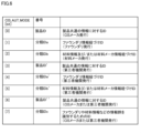
- Figure 2 shows an example of a product ID and a category ID used as ID information.
- the product ID is an ID for information common to all products and is issued by the CIS manufacturer.
- Classification IDa is an ID linked to foundry information and is issued by the foundry.
- Classification IDb is an ID linked to material information and/or material manufacturer information and is issued by the material manufacturer.
- Product ID' is an ID for information common to all products and is issued by a third party.
- Classification ID a' is an ID linked to foundry information and is issued by a third party.
- Classification ID b' is an ID linked to material information and/or material manufacturer information and is issued by a third party.
- Product ID'' is an ID for information common to all products, and is issued by the CIS manufacturer or a third-party organization.
- Classification IDx is an ID for identifying a group of information such as foundry information and material information, and is issued by the CIS manufacturer or a third-party organization.
- classification IDs may be merged for information required in the supply chain, and classification IDa' and classification IDb' are merged to become classification IDx.
- all classification IDs may be merged into the product ID, but there are cases in which this is not possible.
- the CMOS image sensor 32 is designed/manufactured by multiple foundries, or the materials used in the CMOS image sensor 32 are provided by multiple material manufacturers, by linking the product ID with multiple classification IDs, it is possible to match the information disclosed by the CIS manufacturer and link it to information from the foundry, material manufacturer, etc. Then, the CIS manufacturer discloses the minimum necessary information from the multiple linked pieces of information to the customer or user of the final product. At this time, the contents of disclosure can be different for each customer or user.
- the product ID and classification ID stored in the ID information area 64 of the non-rewritable storage unit 43 are used as ID information output from the CMOS image sensor 32 in response to a request for authenticity certification.
- the shipping status and shipping destination data stored in the information area 65 may be output in addition to the ID information.
- the CMOS image sensor 32 is equipped with a register IF (IF functions required to realize the sequence (registers, RAM areas capable of communication, etc.)) as shown in FIG. 3 as a means of communication with the host 31 in order to securely output ID information, etc.
- IF IF functions required to realize the sequence (registers, RAM areas capable of communication, etc.)
- CIS_AUT_REQ is a register IF into which the host 31 writes an authenticity certification request.
- CIS_AUT_REQDATA is a register IF into which the host 31 writes request data (RB
- CIS_AUT_ACKDATA is a register IF into which the host 31 reads response data (TokenAB
- CIS_AUT_MODE is a register IF into which the host 31 writes to select the ID information to be output in the sensor authenticity certification process (output mode selection). For example, it can be set so that when CIS_AUT_MODE is 0, output of all ID information is selected, and when CIS_AUT_MODE is other than 0, output of ID information dependent on the product or market is selected.
- CMOS image sensor 32 has an IF function for other security, it can be configured to be shared with that IF function.
- a data area for other security can be shared and used as an area for writing request data and response data, or security commands can be extended to perform command extension instead of the authenticity certification request register.
- the register IF can be used so that the host 31 receives a one-bit processing state indicating that the authenticity proof process is being executed. Note that registers and signals may be shared with other functions.
- the communication system 11 is configured as described above, and the CMOS image sensor 32 can output the ID information stored in the non-rewritable storage unit 43 from the host 31 in response to an authenticity certification request from the user terminal 12 via the host 31.
- the authenticity of the CMOS image sensor 32 is managed in the user terminal 12 based on the ID information output from the CMOS image sensor 32.
- data encrypted using a common key or a public key can be sent and received between the user terminal 12 and the signature processing unit 44.
- a common key or a public key such as an encrypted sensor authenticity certification request or signature data in which ID information is signed
- the block including the signature processing unit 44 required for signature processing is not always used, so the CMOS image sensor 32 can be configured to start only when a signature is required.
- the supply of power or clock to each block included in the area surrounded by the dashed line in FIG. 1 signature processing unit 44, request receiving area 62, security information area 63, ID information area 64, and information area 65
- the startup register CIS_AUT_ACTV
- the startup register can be turned on to supply power or clock to each block included in the area surrounded by the dashed line in FIG. 1.
- the communication system 11 can securely output information stored in the CMOS image sensor 32, such as ID information.
- ID information For example, using a public key pair stored in the CMOS image sensor 32 and a CA (Certificate Authority) certificate for that public key, a certificate that can only be attached by the CMOS image sensor 32 can be added to the ID information and output to a party outside the module 13, such as the user terminal 12.
- CA Certificate Authority
- the user terminal 12 transmits and receives a sensor authenticity certification request and a sensor authenticity certification response via the host 31 and the communication IF 41 of the CMOS image sensor 32, but there is no need to protect the communication during this process, and a simple sequence will suffice.
- communication following a sequence defined by a general standard from outside the module 13 can be realized through a block having the function of communicating with the CMOS image sensor 32, such as the host 31.
- the simple communication IF itself does not need to have a security function, and for example, a personal computer used in the customer's manufacturing environment can be used.
- Fig. 4 is a block diagram showing a configuration example of a second embodiment of a communication system to which the present technology is applied.
- the communication system 11A shown in Fig. 4 blocks common to the communication system 11 in Fig. 1 are denoted by the same reference numerals, and detailed description thereof will be omitted.
- communication system 11A the user terminal 12 and the host 31 are configured in the same way as in communication system 11 in FIG. 1.
- communication system 11A is configured differently from communication system 11 in FIG. 1 in that the CMOS image sensor 32A is provided with an information output selection unit 46.
- the information output selection unit 46 refers to the CIS_AUT_MODE described above with reference to FIG. 3 to select the ID information output from the CMOS image sensor 32A, reads the ID information from the ID information area 64, and supplies it to the signature processing unit 44.
- the information output selection unit 46 can select the ID information output from the CMOS image sensor 32A by employing any one of the first to third selection methods described below.
- the first method by which the information output selection unit 46 selects ID information is to hold multiple tables in which specific product IDs and classification IDs are registered as ID information, and select which table to output according to CIS_AUT_MODE.
- FIG. 5A shows a table in which a product ID issued by a CIS manufacturer, a classification IDa issued by a foundry, and a classification IDb issued by a material manufacturer are registered as ID information.
- FIG. 5B shows a table in which a product ID' issued by a third party organization, a classification IDa' issued by a third party organization, and a classification IDb' issued by a third party organization are registered as ID information.
- FIG. 5C shows a table in which a product ID'' issued by a CIS manufacturer or a third party organization, and a classification IDx issued by a CIS manufacturer or a third party organization are registered as ID information.
- the second selection method by which the information output selection unit 46 selects ID information is to select which ID information to output by assigning ID information to each bit of CIS_AUT_MODE.
- the ID information to be output can be assigned for each bit of CIS_AUT_MODE.
- the product ID issued by the CIS manufacturer can be assigned to the 0th bit of CIS_AUT_MODE
- the classification ID a issued by the foundry can be assigned to the 1st bit of CIS_AUT_MODE
- the classification ID b issued by the material manufacturer can be assigned to the 2nd bit of CIS_AUT_MODE
- the product ID' issued by a third party can be assigned to the 3rd bit of CIS_AUT_MODE
- the classification ID a' issued by a third party can be assigned to the 4th bit of CIS_AUT_MODE
- the classification ID b' issued by a third party can be assigned to the 5th bit of CIS_AUT_MODE
- the product ID'' issued by the CIS manufacturer or a third party can be assigned to the 6th bit of CIS_AUT_MODE
- the third selection method by which the information output selection unit 46 selects ID information is to select a table as in the first selection method, and then select information to be output from the information in that table. For example, after selecting a table as in the first selection method, it is possible to select which information in the table to output using another register or fuse, etc. For example, it is possible to select to output only the product ID without outputting the classification ID.
- the information output selection unit 46 may select the ID information output from the CMOS image sensor 32A using a selection method other than the first to third selection methods described above.
- the CMOS image sensor 32A can output class information that specifies the disclosure range in addition to the ID information.
- the class information can be signed to set the disclosure level of the ID information output from the CMOS image sensor 32A, including the disclosure level when the user inquires of a third party, thereby restricting the disclosure information.
- the user can then output class information indicating the scope of disclosure together with the ID information to a third-party institution that holds guarantee information such as a certificate.
- a third-party institution that holds guarantee information such as a certificate.
- the class information can be output in a form that cannot be forged, making it possible to restrict the information submitted via the third-party institution.
- step S11 communication is performed according to the interface between the user terminal 12 and the host 31, and the authenticity confirmation unit 22 transmits a sensor authenticity certification request requesting certification of the authenticity of the CMOS image sensor 32A.
- the sensor authenticity certification request includes request data (data [R B ⁇ Text1]) to be written to the security information area 63 (CIS_AUT_REQDATA). Then, when the host 31 completes reception of the sensor authenticity certification request, the process proceeds to step S12.
- step S12 the host 31 communicates with the communication IF 41 and performs data writing to write the request data (data [R B ⁇ Text1]) included in the sensor authenticity certification request to the security information area 63 (CIS_AUT_REQDATA) of the rewritable storage unit 42.
- step S13 the host 31 communicates with the communication IF 41, writes CIS_AUT_MODE to the request receiving area 62 of the rewritable storage unit 42, and sets the disclosure area to be disclosed to the user terminal 12.
- step S14 the host 31 communicates with the communication IF 41, writes an authenticity certification request to the request receiving area 62 (CIS_AUT_REQ) of the rewritable storage unit 42, and issues a signature data generation request to generate signature data in which a signature is applied to the ID information.
- step S15 processing proceeds to step S15.
- step S15 the signature processing unit 44 outputs a processing state indicating the start of the sensor authenticity certification process to the host 31 via the processing state output terminal 45, and the process proceeds to step S16.
- step S16 the CMOS image sensor 32A executes a sensor authenticity certification process.
- the information output selection unit 46 refers to the CIS_AUT_MODE written in the request receiving area 62 by the host 31 in step S13, selects the ID information output from the CMOS image sensor 32A, reads the ID information from the ID information area 64, and supplies it to the signature processing unit 44.
- the signature processing unit 44 signs the ID information supplied from the information output selection unit 46, and writes the signature data with the ID information signed to the security information area 63 of the rewritable storage unit 42.
- the process proceeds to step S17.
- step S17 the signature processing unit 44 outputs a processing state indicating the end of the sensor authenticity certification process to the host 31 via the processing state output terminal 45, and the process proceeds to step S18.
- step S18 the host 31 communicates with the communication IF 41 and performs a data read to read the signature data (data [TokenAB
- step S19 communication is performed according to the interface between the user terminal 12 and the host 31, and the host 31 transmits the signature data (data [TokenAB
- the communication system 11A has a communication area in which data sent from the user terminal 12 can be written, and the host 31 can exchange signature data with a signature applied to the ID information between the user terminal 12 and the CMOS image sensor 32A simply by sending and receiving data through the conventional register communication function.
- the host 31 can have a register or fuse that limits the ID information disclosed from the CMOS image sensor 32A, and can output only the ID information in the CMOS image sensor 32A that the host 31 is willing to disclose.
- a disclosure area is set in step S13 before a signature data generation request is made in step S14.
- the disclosure area is set when the module 13 is incorporated into an electronic device such as a camera, and therefore the process of step S13 for setting the disclosure area can be skipped.
- FIG. 8 is a block diagram showing a configuration example of a communication system according to a third embodiment of the present technology.
- blocks common to the communication system 11 in Fig. 1 are denoted by the same reference numerals, and detailed description thereof will be omitted.
- communication system 11B the user terminal 12 and the host 31 are configured in the same way as in communication system 11 in FIG. 1.
- communication system 11B is configured differently from communication system 11 in FIG. 1 in that CMOS image sensor 32B includes signature processing unit 44B and output IF 53B.
- the signature processing unit 44B performs a signature process to apply a signature to the ID information read from the ID information area 64 of the non-rewriteable storage unit 43, and supplies the signature data with the ID information signed to the output IF 53B.
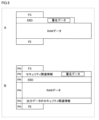
- the output IF 53B inserts the signature data supplied from the signature processing unit 44B into a predetermined location in the format used when outputting image data from the CMOS image sensor 32B, and outputs the image data and signature data together.
- SLVS-EC Scalable Low Voltage Signaling with Embedded Clock
- MIPI Mobile Industry Processor Interface
- ESD embedded Data
- the output IF 53B can insert signature data into this embedded data area.
- the output IF 53B can insert signature data into the area that outputs the SLVS-EC security-related information, as shown in FIG. 9B.
- the signature data can be added to the image data and output via the output IF 53B.
- the signature data added to the image data can then be output to the user terminal 12 via the host 31.
- a CIS manufacturer manufactures a CMOS image sensor 32 in which a classification IDa issued by a foundry, a classification IDb issued by a materials manufacturer, and a classification IDc issued by an equipment manufacturer are written in the ID information area 64, and ships it to a manufacturing plant that produces the final product.
- the CIS manufacturer confirms in advance that the requirements are met based on information from each of the foundry, materials manufacturer, and equipment manufacturer, as well as their databases, and then procures the design, materials, and equipment.
- the foundry, material manufacturer, and equipment manufacturer request the third-party organization to issue classification IDa, classification IDb, and classification IDc, respectively.
- the third-party organization manages the certificates by linking them to classification IDa, classification IDb, and classification IDc.
- a final product such as an electronic device equipped with the CMOS image sensor 32 is manufactured in a manufacturing factory, and the user can obtain the final product.
- the user can then use the user terminal 12 to perform the communication process described with reference to FIG. 7 to read out the ID information (classification IDa, classification IDb, and classification IDc) from the CMOS image sensor 32 and obtain the necessary certificate from a third-party organization.
- the user can align the product-related information of the CMOS image sensor 32 based on the ID information read out from the CMOS image sensor 32.
- the certificate can be obtained while keeping the identity of the outsourced company confidential from the user or customer.
- the user can confirm that the certificates for design, materials, equipment, etc. are linked to the actual final product based on the ID information (classification IDa, classification IDb, and classification IDc) read from the CMOS image sensor 32. This allows the user to confirm, for example, whether or not parts that comply with the policy are being used.
- the certificates may be managed in the databases of the foundry, material manufacturer, and equipment manufacturer.
- the shipping status and purchase destination information described below can be written to the non-rewritable storage unit 43 and output together with the ID information.
- the output of the shipping status and purchase destination information described below can also be switched on/off using an option mode register (CIS_OPT_MODE) or the like.
- the shipping status can be a status that indicates whether the product is a sample product, a discarded product (for example, a product that does not meet the quality standards), or a product for sale.
- the shipping status can be used to manage regular sales products, sample products, discarded products (products that do not meet the conditions for reliability, etc. and are to be discarded), etc.
- the sales destination information information for managing sales destinations for internal identification can be used.
- the sales destination information can be used to manage the distribution route in the case where the CMOS image sensor 32 is used in a market other than that covered by the contract.
- an area that can be updated by the customer may be provided in the non-rewritable storage unit 43.
- the customer can update the disposal status by blowing a fuse in the non-rewritable storage unit 43 when disposing of the CMOS image sensor 32.
- the disposal status has been updated in the non-rewritable storage unit 43, it becomes impossible to update the information thereafter. This makes it possible, for example, to illegally manage waste disposal companies.
- information such as data for linking generation conditions input from a user or the like via the communication IF 41 can be signed together with ID information and output.
- information for identifying the data recipient such as a user ID or timestamp
- a signature can be applied including this information.
- the timestamp can be confirmed when making an inquiry to a third-party institution.
- the user terminal 12 makes this information part of the random number (R B ) input from the register IF, or puts it in the information of Text1, and transmits it to the CMOS image sensor 32.
- the CMOS image sensor 32 then merges the information transmitted from the user terminal 12 with information such as the ID, applies a signature to the entire data, and outputs it.
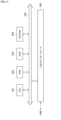
- FIG. 11 is a block diagram showing an example of the hardware configuration of a computer that executes the above-mentioned series of processes using a program.
- a CPU Central Processing Unit
- ROM Read Only Memory
- RAM Random Access Memory
- EEPROM Electrically Erasable and Programmable Read Only Memory
- the CPU 101 loads, for example, programs stored in the ROM 102 and EEPROM 104 into the RAM 103 via the bus 105 and executes them, thereby carrying out the above-mentioned series of processes. Furthermore, the programs executed by the computer (CPU 101) can be written in advance into the ROM 102, or can be installed or updated in the EEPROM 104 from the outside via the input/output interface 106.
- the processing performed by a computer according to a program does not necessarily have to be performed in chronological order according to the order described in the flowchart.
- the processing performed by a computer according to a program also includes processing that is executed in parallel or individually (for example, parallel processing or processing by objects).
- the program may be processed by one computer (processor), or may be distributed among multiple computers. Furthermore, the program may be transferred to a remote computer for execution.
- a system refers to a collection of multiple components (devices, modules (parts), etc.), regardless of whether all the components are in the same housing. Therefore, multiple devices housed in separate housings and connected via a network, and a single device in which multiple modules are housed in a single housing, are both systems.
- the configuration described above as one device (or processing unit) may be divided and configured as multiple devices (or processing units).
- the configurations described above as multiple devices (or processing units) may be combined and configured as one device (or processing unit).
- configurations other than those described above may also be added to the configuration of each device (or each processing unit).
- part of the configuration of one device (or processing unit) may be included in the configuration of another device (or other processing unit).
- this technology can be configured as cloud computing, in which a single function is shared and processed collaboratively by multiple devices via a network.
- the above-mentioned program can be executed in any device.
- the device has the necessary functions (functional blocks, etc.) and is able to obtain the necessary information.
- each step described in the above flowchart can be executed by one device, or can be shared and executed by multiple devices.
- one step includes multiple processes, the multiple processes included in that one step can be executed by one device, or can be shared and executed by multiple devices.
- multiple processes included in one step can be executed as multiple step processes.
- processes described as multiple steps can be executed collectively as one step.
- processing of the steps that describe a program executed by a computer may be executed chronologically in the order described in this specification, or may be executed in parallel, or individually at the required timing, such as when a call is made. In other words, as long as no contradictions arise, the processing of each step may be executed in an order different from the order described above. Furthermore, the processing of the steps that describe this program may be executed in parallel with the processing of other programs, or may be executed in combination with the processing of other programs.
- the present technology can also be configured as follows.
- a communication interface for communicating with a host in accordance with a predetermined communication standard; a non-rewritable storage unit that stores ID (Identification) information in a state that cannot be rewritten at the time of shipment, a semiconductor chip that outputs the ID information stored in the non-rewritable storage unit from the communication interface in response to a request from an external terminal via the host.
- ID information Identity
- the semiconductor chip according to (1) or (2) above further comprising: a shipping status and shipping destination data of the semiconductor chip, which are added to the ID information.
- the semiconductor chip described in any one of (1) to (3) above further comprising an information output selection unit that selects the ID information to be output from the communication interface from among the plurality of ID information stored in the non-rewritable memory unit.
- the semiconductor chip according to any one of (1) to (4) above further comprising a signature processing unit that performs a signature process for applying a signature to the ID information by encrypting the ID information using a key, and outputs signature data with the ID information signed from the communication interface.
- the request transmitted from the external terminal is encrypted with a first key
- the signature processing unit decrypts the request using a second key corresponding to the first key.
- the signature processing unit inserts the signature data into a predetermined location in a format when outputting image data, and outputs the image data with the signature data added thereto.
- power or a clock is supplied to a block including the signature processing unit required for the signature processing only when the signature processing is performed.
- the semiconductor chip a communication interface for communicating with a host in accordance with a predetermined communication standard; a non-rewritable storage unit that stores ID (Identification) information in a state that cannot be rewritten at the time of shipment, outputting the ID information stored in the non-rewritable storage unit from the communication interface in response to a request from an external terminal via the host.
- ID Identification
- a communication interface for communicating with a host in accordance with a predetermined communication standard; a non-rewritable storage unit that stores ID (Identification) information in a state that cannot be rewritten at the time of shipment; an external terminal that transmits a request via the host, In response to the request, the ID information stored in the non-rewritable storage unit is output from the communication interface.
Landscapes
- Engineering & Computer Science (AREA)
- Physics & Mathematics (AREA)
- Computer Hardware Design (AREA)
- Computer Security & Cryptography (AREA)
- Theoretical Computer Science (AREA)
- Mathematical Physics (AREA)
- Software Systems (AREA)
- General Engineering & Computer Science (AREA)
- General Physics & Mathematics (AREA)
- Computer Networks & Wireless Communication (AREA)
- Signal Processing (AREA)
- Storage Device Security (AREA)
Abstract
本開示は、半導体チップの真正性の管理を確実に行うことができるようにする半導体チップ、通信方法、および通信システムに関する。 通信インタフェースは、ホストとの間で、所定の通信規格に従って通信を行い、書き換え不可記憶部は、出荷時には書き換えることが不可となる状態でID情報を記憶する。そして、ホストを介した外部の端末からのリクエストに応じて、書き換え不可記憶部に記憶されているID情報が通信インタフェースから出力される。本技術は、例えば、CMOSイメージセンサの真正性を確認する通信システムに適用できる。
Description
本開示は、半導体チップ、通信方法、および通信システムに関し、特に、半導体チップの真正性の管理を確実に行うことができるようにした半導体チップ、通信方法、および通信システムに関する。
近年、CMOS(Complementary Metal-Oxide-Semiconductor)イメージセンサなどの半導体チップを含む様々な部品のトレーサビリティの必要性が強く求められている。例えば、CMOSイメージセンサでは、CMOSイメージセンサ自体やCMOSイメージセンサの製造に関わる製造環境および材料など、市場が求める情報が紐づけられるような機能が必要とされている。
従来、特許文献1で開示されているように、イメージセンサおよびホスト(アプリケーションプロセッサ)の間で安全性の高い通信を行う技術が提案されている。
ところで、従来の技術では、イメージセンサと、イメージセンサに直接的に接続されるホストとの間でセキュリティを前提とした通信を行うことができるのに対し、イメージセンサと、外部のユーザ端末との間でセキュリティを前提とした通信を行うことはできなかった。そのため、イメージセンサが保持している情報が正しいことをホストが確認することはできても、イメージセンサが保持している情報が正しいことを外部のユーザ端末は確認することができず、例えば、外部のユーザ端末でイメージセンサの真正性を管理することは困難であった。
本開示は、このような状況に鑑みてなされたものであり、半導体チップの真正性の管理を確実に行うことができるようにするものである。
本開示の一側面の半導体チップは、ホストとの間で、所定の通信規格に従って通信を行う通信インタフェースと、出荷時には書き換えることが不可となる状態でID情報を記憶する書き換え不可記憶部とを備え、前記ホストを介した外部の端末からのリクエストに応じて、前記書き換え不可記憶部に記憶されている前記ID情報を前記通信インタフェースから出力する。
本開示の一側面の通信方法は、半導体チップが、ホストとの間で、所定の通信規格に従って通信を行う通信インタフェースと、出荷時には書き換えることが不可となる状態でID情報を記憶する書き換え不可記憶部とを備え、前記ホストを介した外部の端末からのリクエストに応じて、前記書き換え不可記憶部に記憶されている前記ID情報を前記通信インタフェースから出力することを含む。
本開示の一側面の通信システムは、ホストとの間で、所定の通信規格に従って通信を行う通信インタフェースと、出荷時には書き換えることが不可となる状態でID情報を記憶する書き換え不可記憶部とを有する半導体チップと、前記ホストを介してリクエストを送信する外部の端末とを備える通信システムであって、前記リクエストに応じて、前記書き換え不可記憶部に記憶されている前記ID情報を前記通信インタフェースから出力する。
本開示の一側面においては、ホストとの間で、所定の通信規格に従って通信が通信インタフェースによって行われ、出荷時には書き換えることが不可となる状態でID情報が書き換え不可記憶部に記憶される。そして、ホストを介した外部の端末からのリクエストに応じて、書き換え不可記憶部に記憶されているID情報が通信インタフェースから出力される。
以下、本技術を適用した具体的な実施の形態について、図面を参照しながら詳細に説明する。
<通信システムの第1の構成例>
図1は、本技術を適用した通信システムの第1の実施の形態の構成例を示すブロック図である。
図1は、本技術を適用した通信システムの第1の実施の形態の構成例を示すブロック図である。
図1に示す通信システム11は、ユーザ端末12がモジュール13と通信を行うことによって、モジュール13に搭載されたCMOSイメージセンサ32の真正性の管理を行うことができる。
ユーザ端末12は、起動確認部21および真正性確認部22を備えて構成され、例えば、モジュール13が搭載された電子機器などの最終製品を使用するユーザが、モジュール13が備えるCMOSイメージセンサ32の真正性を確認する際に用いられる。また、ユーザ端末12は、モジュール13内に設けられるホスト31を介して、CMOSイメージセンサ32との間で、共通鍵、公開鍵、秘密鍵、またはセッション鍵を用いて暗号化されたデータの送受信を行うことができる。
起動確認部21は、モジュール13のホスト31と通信を行って、CMOSイメージセンサ32が起動していることの確認を要求する起動確認リクエストを送信し、CMOSイメージセンサ32が起動していることを通知する起動通知レスポンスを受信する。そして、起動確認部21は、CMOSイメージセンサ32が起動していることを確認すると、そのことを真正性確認部22に通知する。
真正性確認部22は、CMOSイメージセンサ32が起動していることが起動確認部21によって確認されると、CMOSイメージセンサ32の真正性の証明を要求するセンサ真正性証明リクエストをモジュール13のホスト31に送信する。そして、真正性確認部22は、CMOSイメージセンサ32においてセンサ真正性証明処理が行われた結果としてホスト31から送信されてくるセンサ真正性証明レスポンスを受信する。
モジュール13は、ホスト31およびCMOSイメージセンサ32を備えて構成される。
ホスト31は、ユーザ端末12およびCMOSイメージセンサ32との間で、それぞれ通信を行うことができる。例えば、ホスト31は、CMOSイメージセンサ32の通信IF41との間では、SPI(Serial Peripheral Interface)や、I2C(Inter-Integrated Circuit)、I3C(Improved Inter Integrated Circuit)などの通信規格に従って通信を行う。ホスト31は、CMOSイメージセンサ32の起動を確認する機能(例えば、WDT(Watch Dog Timer)の開始タイミングを知るための機能)や、CMOSイメージセンサ32の真正性の証明を受け付けるための機能(例えば、センサ真正性証明リクエストや、真正性の証明のために必要なランダムデータなどを受け取る機能)などを備えている。
例えば、ホスト31は、起動確認部21から送信されてくる起動確認リクエストを受信した場合に、CMOSイメージセンサ32が起動していなかったとき、CMOSイメージセンサ32の電源を投入して起動シーケンスを実行させることができる。そして、ホスト31は、CMOSイメージセンサ32を起動させた後、または、CMOSイメージセンサ32が起動していた場合、起動通知レスポンスを起動確認部21に送信する。
例えば、ホスト31は、真正性確認部22から送信されてくるセンサ真正性証明リクエストを受信すると、CMOSイメージセンサ32の定めるシーケンスに沿ってレジスタ通信を行うことができる。ここで、ホスト31は、CMOSイメージセンサ32のレジスタに対するライトまたはリードのみを基本的に行うことができればよく、一般的なホストが備える機能を用いてCMOSイメージセンサ32と通信を行うことが可能である。そして、ホスト31とCMOSイメージセンサ32との間の通信自体にセキュリティ機能が必要とされることはない。例えば、通信システム11においてセキュリティ機能が必要なのは、署名を行うCMOSイメージセンサ32と、その署名の検証を行うユーザ端末12であるので、ホスト31とCMOSイメージセンサ32との間でセキュリティ機能を搭載していても、そのセキュリティ機能が準備できていない状態(例えば、起動直後の状態など)でも動作することができる。
CMOSイメージセンサ32は、通信IF(Interface)41、書き換え可能記憶部42、書き換え不可記憶部43、署名処理部44、および処理ステート出力端子45を備えて構成される。さらに、CMOSイメージセンサ32は、画素値を出力する画素51、画素51から出力される画素値により構成される画像データに対するデータ処理を施すデータ処理部52、および、データ処理部52でデータ処理が施された画像データを所定のフォーマットで外部に出力する出力IF53を備えている。
通信IF41は、ホスト31との間で、SPIや、I2C,I3Cなどの通信規格に従って通信を行うことができ、ホスト31から送信されてきたデータを書き換え可能記憶部42に書き込む。
書き換え可能記憶部42は、例えば、不揮発メモリなどにより構成され、通信IF41を介して書き込まれるデータを記憶する。例えば、書き換え可能記憶部42には、CMOSイメージセンサ32に対する各種の設定を記憶するレジスタ61、ユーザ端末12から送信されてきたセンサ真正性証明リクエストなどを記憶するリクエスト受信領域62、および、CMOSイメージセンサ32から出力されるセンサ真正性証明レスポンスなどを記憶するセキュリティ情報領域63が設けられる。
書き換え不可記憶部43は、例えば、CMOSイメージセンサ32の出荷時には書き換えることが不可となるヒューズ型PROM(Programmable ROM)により構成され、CMOSイメージセンサ32が出荷された後、書き換えを禁止すべきデータを記憶する。例えば、書き換え不可記憶部43には、ID(Identification)情報を記憶するID情報領域64、および、ID情報以外の情報を記憶する情報領域65が設けられる。
署名処理部44は、ユーザ端末12から送信されてきたセンサ真正性証明リクエストに応じて、書き換え不可記憶部43のID情報領域64から読み出したID情報を共通鍵または公開鍵を用いて暗号化することによって署名を施す署名処理を行って、ID情報に署名が施された署名データを、セキュリティ情報領域63に記憶させる。セキュリティ情報領域63に記憶された署名データは、真正性確認部22において、署名処理部44が用いた共通鍵または公開鍵に対応する秘密鍵を用いて復号することができる。一方、ユーザ端末12から送信されてくるセンサ真正性証明リクエストは共通鍵または公開鍵(第1の鍵)によって暗号化されており、署名処理部44は、暗号化されているセンサ真正性証明リクエストを、その暗号化に用いられた共通鍵または公開鍵に対応する秘密鍵(第2の鍵)を用いて復号することができる。さらに、署名処理部44は、センサ真正性証明処理を開始または終了を示す処理ステートを、処理ステート出力端子45を介してホスト31に出力する。なお、ID情報に適用される暗号化方式やセンサ真正性証明リクエストに適用される暗号化方式は、上記に限定されず、例えばセッション鍵暗号方式が用いられてもよい。
ここで、書き換え不可記憶部43は、例えば、CMOSイメージセンサ32の実装時に情報を反映させたり、CMOSイメージセンサ32の製造時に情報を書き込んだりした後、ヒューズを切断することによって情報の書き換えができない状態となるように構成される。従って、CMOSイメージセンサ32の出荷時には、書き換え不可記憶部43に書き込まれた情報を書き換え不可とすることができる。
書き換え不可記憶部43の情報領域65に記憶されるデータには、例えば、後述するクラス情報や、ユーザ端末12などからの生成条件紐づけのためのデータ、出荷時におけるCMOSイメージセンサ32の状態を示す出荷ステータス、CMOSイメージセンサ32の販売先を示す出荷先データなどが含まれる。これらのデータは、個体評価結果や購入先などが決定した時点で書き込むことができるため、ヒューズを切断することによって情報の書き換えが不可となる書き換え不可記憶部43に書き込んだ後、CMOSイメージセンサ32が出荷される。
書き換え不可記憶部43のID情報領域64に記憶されるID情報として、製品IDおよび分類IDが少なくとも用いられる。
製品IDは、CMOSイメージセンサ32としての製品を識別するためのIDである。即ち、製品IDは、CMOSイメージセンサ32の製品共通の情報に対するIDであって、CMOSイメージセンサ32を製造したメーカ(以下、CISメーカと称する)に関する情報が含まれている。
分類IDは、CMOSイメージセンサ32の製造環境や材料などに紐づけられるID(または複数のIDからなるID群)である。例えば、複数のチップが積層された積層型のCMOSイメージセンサ32では、それぞれのチップが異なるファウンダリで設計/製造されることがあり、CMOSイメージセンサ32の分類IDとして、それらのファウンダリに紐づけられた複数のIDが用いられる。その他、分類IDには、市場で求められる各種の情報が紐づけられるようにしてもよい。
なお、ID情報には、CMOSイメージセンサ32を個別に識別するための個体識別IDが含まれていてもよい。例えば、ID情報に個体識別IDを含めることは必須ではないが、ID情報に個体識別IDを含めることによってセキュリティを高めることができる。
ID情報に含まれる製品IDおよび分類IDは、それぞれ発行元が異なるケースがあり、例えば、CISメーカ、第三者機関、または、委託先(ファウンダリや、装置メーカ、材料メーカなど)により発行される。なお、発行元に従って、製品IDおよび分類IDの出力を切り替えてもよい。
また、CISメーカにより発行される製品IDおよび分類IDを用いる場合、あるいは、CISメーカが製造環境などの情報もマージして第三者機関に新たに認証を受ける場合、製品IDを製造環境や材料メーカごとに変えることで、製造環境や材料メーカなどの情報を製品IDにまとめること、即ち、複数の分類IDをマージすることができる。例えば、製品IDに全ての分類IDをマージしてもよいが、それぞれの分類IDを分けることによって必要な情報だけを顧客が使用できるようにすることが好適である。
図2には、ID情報として用いられる製品IDおよび分類IDの一例が示されている。
例えば、製品IDは、製品共通の情報に対するIDであって、CISメーカにより発行されたものである。分類IDaは、ファウンダリ情報に紐づけられるIDであって、ファウンダリにより発行されたものである。分類IDbは、材料情報及び/または材料メーカ情報に紐づけられるIDであって、材料メーカにより発行されたものである。
製品ID’は、製品共通の情報に対するIDであって、第三者機関により発行されたものである。分類IDa’は、ファウンダリ情報に紐づけられるIDであって、第三者機関により発行されたものである。分類IDb’は、材料情報及び/または材料メーカ情報に紐づけられるIDであって、第三者機関により発行されたものである。
製品ID’’は、製品共通の情報に対するIDであって、CISメーカまたは第三者機関により発行されたものである。分類IDxは、ファウンダリ情報や材料情報などの情報群を識別するためのIDであって、CISメーカまたは第三者機関により発行されたものである。つまり、サプライチェーンで必要な情報について分類IDをマージしてもよく、分類IDa’および分類IDb’をマージしたものが分類IDxとなる。さらに、製品IDに、全ての分類IDをマージしてもよいが、マージできない場合もある。
例えば、複数のファウンダリでCMOSイメージセンサ32を設計/製造したり、CMOSイメージセンサ32に使用される材料が複数の材料メーカから提供されたりする場合、製品IDと複数の分類IDとを紐づけることで、CISメーカが開示した情報と照合して、ファウンダリや材料メーカなどの情報と紐づけることができる。そして、CISメーカは、紐づけられた複数の情報のうちの必要最低限の情報を、顧客や最終製品のユーザに開示する。このとき、開示内容は、顧客やユーザごとに異なるものとすることができる。
このように書き換え不可記憶部43のID情報領域64に記憶されている製品IDおよび分類IDが、真正性証明リクエストに応じてCMOSイメージセンサ32から出力されるID情報として用いられる。また、ID情報に付加して、情報領域65に記憶されている出荷ステータスおよび出荷先データを出力してもよい。
図3を参照して、CMOSイメージセンサ32が備えるIF機能について説明する。
CMOSイメージセンサ32は、ID情報などをセキュアに出力するために、ホスト31との通信手段として、図3に示すようなレジスタIF(シーケンスを実現するために必要なIF機能(レジスタや通信可能なRAM領域など))を備えている。
図3のAに示すように、CIS_AUT_REQは、ホスト31が真正性証明リクエストを書き込むレジスタIFである。CIS_AUT_REQDATAは、ホスト31がリクエストデータ(RB || Text1)を書き込むレジスタIFである。CIS_AUT_ACKDATAは、ホスト31がレスポンスデータ(TokenAB || CertA)を読み出すレジスタIFである。CIS_AUT_MODEは、センサ真正性証明処理で出力するID情報を選択(出力モード選択)するためにホスト31が書き込むレジスタIFである。例えば、CIS_AUT_MODEが0の場合には、全てのID情報を出力することが選択され、CIS_AUT_MODEが0以外の場合には、製品や市場に依存したID情報を出力することが選択されるように設定することができる。
なお、CMOSイメージセンサ32が他のセキュリティのためのIF機能を備える場合、そのIF機能と共有して用いられる構成とすることができる。例えば、他のセキュリティ用のデータ領域をリクエストデータおよびレスポンスデータを書き込む領域として共有化して使用したり、セキュリティコマンドを拡張して真正性証明リクエストレジスタの代わりにコマンド拡張を行ったりしてもよい。
また、上述したように、処理ステート出力端子45を介して処理ステートをホスト31に出力する他、図3のBに示すように、真正性証明処理の実行中であることを示す1ビットの処理ステートをホスト31が受け取るようにレジスタIFを利用することができる。なお、他の機能とレジスタや信号を共有してもよい。
以上のように通信システム11は構成されており、CMOSイメージセンサ32は、ホスト31を介したユーザ端末12からの真正性証明リクエストに応じて、書き換え不可記憶部43に記憶されているID情報をホスト31から出力することができる。そして、通信システム11では、CMOSイメージセンサ32から出力されるID情報に基づいて、ユーザ端末12においてCMOSイメージセンサ32の真正性の管理が行われることになる。
さらに、通信システム11では、ユーザ端末12と署名処理部44との間で、共通鍵または公開鍵を用いて暗号化したデータ(暗号化されたセンサ真正性証明リクエストや、ID情報に署名が施された署名データなど)の送受信を行うことができる。これにより、通信システム11では、CMOSイメージセンサ32に直接的に接続されていないユーザ端末12との間でセキュアに通信を行うことが可能となり、より確実に、CMOSイメージセンサ32の真正性の管理を行うことができる。
なお、通信システム11では、署名処理に必要となる署名処理部44を含むブロックは常に使用されるわけではないので、署名が必要なときにだけ起動するようにCMOSイメージセンサ32を構成することができる。つまり、図1において一点鎖線で囲われた領域に含まれる各ブロック(署名処理部44、リクエスト受信領域62、セキュリティ情報領域63、ID情報領域64、および情報領域65)に対して、通常時には電源またはクロックの供給が停止される。そして、署名処理が行われるときのみ、例えば、ユーザ端末12から起動要求があった場合に起動用のレジスタ(CIS_AUT_ACTV)をオンにして、図1において一点鎖線で囲われた領域に含まれる各ブロックに対して、電源またはクロックの供給が行われるようにすることができる。
また、通信システム11では、ID情報などのCMOSイメージセンサ32内の情報をセキュアに出力することができる。例えば、CMOSイメージセンサ32内の公開鍵ペアとその公開鍵のCA(Certificate Authority)認証書により、ユーザ端末12などのようにモジュール13外の相手に対して、CMOSイメージセンサ32のみが付けることのできる証明書をID情報に付加して出力する。
なお、通信システム11では、ユーザ端末12は、ホスト31とCMOSイメージセンサ32の通信IF41とを介して、センサ真正性証明リクエストおよびセンサ真正性証明レスポンスの送受信を行うが、その際の通信を保護する必要はなく、簡易的なシーケンスでよい。つまり、通信システム11では、ホスト31などのCMOSイメージセンサ32と通信する機能を有するブロックを通して、モジュール13の外部から、一般的な規格で定められたシーケンスに従った通信が実現されればよい。
また、顧客の製造環境などで、CMOSイメージセンサ32の真正性の確認(真贋判定)を行うときには、簡易的な通信IF自身はセキュリティ機能を備える必要はなく、例えば、顧客の製造環境で用いられているパーソナルコンピュータなどを使用することができる。
<通信システムの第2の構成例>
図4は、本技術を適用した通信システムの第2の実施の形態の構成例を示すブロック図である。なお、図4に示す通信システム11Aにおいて、図1の通信システム11と共通するブロックについては、同一の符号を付し、その詳細な説明は省略する。
図4は、本技術を適用した通信システムの第2の実施の形態の構成例を示すブロック図である。なお、図4に示す通信システム11Aにおいて、図1の通信システム11と共通するブロックについては、同一の符号を付し、その詳細な説明は省略する。
即ち、通信システム11Aでは、ユーザ端末12およびホスト31は、図1の通信システム11と同様に構成されている。一方、通信システム11Aでは、CMOSイメージセンサ32Aが、情報出力選択部46を備えている点で、図1の通信システム11と異なる構成となっている。
情報出力選択部46は、図3を参照して上述したCIS_AUT_MODEを参照して、CMOSイメージセンサ32Aから出力されるID情報を選択し、そのID情報をID情報領域64から読み出して署名処理部44に供給する。例えば、情報出力選択部46は、以下で説明するような第1乃至第3の選択方法いずれかを採用して、CMOSイメージセンサ32Aから出力されるID情報を選択することができる。
情報出力選択部46がID情報を選択する第1の選択方法は、所定の製品IDおよび分類IDがID情報として登録された複数のテーブルを保持しておき、CIS_AUT_MODEに従って、どのテーブルを出力するのかを選択する方法である。
例えば、第1の選択方法では、図5に示すような3つのテーブルが保持される。図5のAには、CISメーカにより発行された製品ID、ファウンダリにより発行された分類IDa、および、材料メーカにより発行された分類IDbが、ID情報として登録されたテーブルが示されている。図5のBには、第三者機関により発行された製品ID’、第三者機関により発行された分類IDa’、および、第三者機関により発行された分類IDb’が、ID情報として登録されたテーブルが示されている。図5のCには、CISメーカまたは第三者機関により発行された製品ID’’、および、CISメーカまたは第三者機関により発行された分類IDxが、ID情報として登録されたテーブルが示されている。
そして、情報出力選択部46は、CIS_AUT_MODE=0である場合には、図5のAに示したテーブルを選択し、CIS_AUT_MODE=1である場合には、図5のBに示したテーブルを選択し、CIS_AUT_MODE=2である場合には、図5のCに示したテーブルを選択する。
情報出力選択部46がID情報を選択する第2の選択方法は、CIS_AUT_MODEのビットごとに出力するID情報を割り当てることで、どのID情報を出力するのかを選択する方法である。
例えば、第2の選択方法では、図6に示すように、CIS_AUT_MODEのビットごとに出力するID情報を割り当てることができる。例えば、CIS_AUT_MODEの0ビット目には、CISメーカにより発行された製品IDを割り当て、CIS_AUT_MODEの1ビット目には、ファウンダリにより発行された分類IDaを割り当て、CIS_AUT_MODEの2ビット目には、材料メーカにより発行された分類IDbを割り当て、CIS_AUT_MODEの3ビット目には、第三者機関により発行された製品ID’を割り当て、CIS_AUT_MODEの4ビット目には、第三者機関により発行された分類IDa’を割り当て、CIS_AUT_MODEの5ビット目には、第三者機関により発行された分類IDb’を割り当て、CIS_AUT_MODEの6ビット目には、CISメーカまたは第三者機関により発行された製品ID’’を割り当て、CIS_AUT_MODEの7ビット目には、CISメーカまたは第三者機関により発行された分類IDxを割り当てることができる。
そして、情報出力選択部46は、CIS_AUT_MODEの各ビットが1である場合には、そのビットに割り当てられたID情報を出力し、CIS_AUT_MODEの各ビットが0である場合には、そのビットに割り当てられたID情報を出力しない。具体的には、CIS_AUT_MODEの0ビット目が1である場合には製品IDが出力され、CIS_AUT_MODEの3ビット目が0である場合には製品ID’は出力されない。
情報出力選択部46がID情報を選択する第3の選択方法は、第1の選択方法と同様にテーブルを選択した後、そのテーブル内の情報からさらに出力する情報を選択する方法である。例えば、第1の選択方法と同様にテーブルを選択した後、そのテーブル内のどの情報を出力するかを、別のレジスタまたはヒューズなどで選択することができる。例えば、分類IDは出力せずに、製品IDのみを出力するような選択を行うことができる。
もちろん、情報出力選択部46は、上述したような第1乃至第3の選択方法以外の選択方法で、CMOSイメージセンサ32Aから出力されるID情報を選択してもよい。
さらに、CMOSイメージセンサ32Aは、ID情報の出力時に、ID情報以外に開示範囲を指定するクラス情報を、ID情報とともに出力することができる。例えば、クラス情報では、CMOSイメージセンサ32Aから出力されるID情報の開示レベルの設定として、ユーザが第三者機関に問い合わせる際の開示レベルまで含めて署名することで、開示情報を制限することができる。
そして、ユーザは、証明書などの保証情報を保持する第三者機関に、開示範囲を示すクラス情報をID情報と一緒に出力することができる。このとき、クラス情報にも署名処理部44によって署名を施すことにより、クラス情報を偽造できない形で出力することができ、第三者機関を通じて提出する情報への制約を行うことが可能となる。
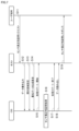
図7に示すシーケンス図を参照して、通信システム11Aにおいて行われる通信処理の一例について説明する。
例えば、CMOSイメージセンサ32Aの起動の確認が行われた後、ステップS11において、ユーザ端末12およびホスト31の間のインタフェースに従った通信が行われ、真正性確認部22は、CMOSイメージセンサ32Aの真正性の証明を要求するセンサ真正性証明リクエストを送信する。センサ真正性証明リクエストには、セキュリティ情報領域63(CIS_AUT_REQDATA)に書き込まれるリクエストデータ(データ[RB || Text1])が含まれている。そして、ホスト31が、センサ真正性証明リクエストの受信を完了すると処理はステップS12に進む。
ステップS12において、ホスト31は、通信IF41との間で通信を行って、書き換え可能記憶部42のセキュリティ情報領域63(CIS_AUT_REQDATA)に、センサ真正性証明リクエストに含まれていたリクエストデータ(データ[RB || Text1])を書き込むデータ書き込みを行う。
ステップS13において、ホスト31は、通信IF41との間で通信を行って、書き換え可能記憶部42のリクエスト受信領域62にCIS_AUT_MODEを書き込み、ユーザ端末12に対して開示すべき開示領域を設定する開示領域設定を行う。
ステップS14において、ホスト31は、通信IF41との間で通信を行って、書き換え可能記憶部42のリクエスト受信領域62(CIS_AUT_REQ)に真正性証明リクエストを書き込み、ID情報に署名が施された署名データの生成を要求する署名データ生成要求を行う。
そして、ステップS12乃至S14の処理が完了すると、処理はステップS15に進む。
ステップS15において、署名処理部44は、処理ステート出力端子45を介して、センサ真正性証明処理の開始を示す処理ステートをホスト31に出力し、処理はステップS16に進む。
ステップS16において、CMOSイメージセンサ32Aではセンサ真正性証明処理が実行される。センサ真正性証明処理において、情報出力選択部46は、ステップS13でホスト31によりリクエスト受信領域62に書き込まれたCIS_AUT_MODEを参照して、CMOSイメージセンサ32Aから出力されるID情報を選択し、そのID情報をID情報領域64から読み出して署名処理部44に供給する。署名処理部44は、情報出力選択部46から供給されたID情報に対して署名を施し、ID情報に署名が施された署名データを、書き換え可能記憶部42のセキュリティ情報領域63に書き込む。これにより、センサ真正性証明処理が完了すると、処理はステップS17に進む。
ステップS17において、署名処理部44は、処理ステート出力端子45を介して、センサ真正性証明処理の終了を示す処理ステートをホスト31に出力し、処理はステップS18に進む。
ステップS18において、ホスト31は、通信IF41との間で通信を行って、書き換え可能記憶部42のセキュリティ情報領域63(CIS_AUT_ACKDATA)に書き込まれている署名データ(データ[TokenAB || CertA])を読み出すデータ読み出しを行う。
ステップS19において、ユーザ端末12およびホスト31の間のインタフェースに従った通信が行われ、ホスト31は、書き換え可能記憶部42のセキュリティ情報領域63(CIS_AUT_ACKDATA)から読み出した署名データ(データ[TokenAB || CertA])を、センサ真正性証明レスポンスとして送信する。そして、ユーザ端末12の真正性確認部22がセンサ真正性証明レスポンスを受信すると処理は終了される。
以上のように、通信システム11Aでは、ユーザ端末12から送信されてくるデータを書き込み可能な通信領域を持つことで、ホスト31が、従来のレジスタ通信機能を通じてデータを送受信するだけで、ユーザ端末12およびCMOSイメージセンサ32Aの間で、ID情報に署名が施された署名データをやり取りすることができる。
また、通信システム11Aでは、ホスト31が、CMOSイメージセンサ32Aから開示されるID情報を制限するレジスタまたはヒューズを持つことで、CMOSイメージセンサ32A内のID情報のうち、ホスト31が開示してよいID情報のみを出力させることができる。例えば、レジスタの場合、ステップS14で署名データ生成要求を行う前に、ステップS13で開示領域設定が行われる。なお、ヒューズの場合、カメラなどの電子機器へのモジュール13の組み込み時に開示領域設定が行われるため、開示領域設定を行うステップS13の処理はスキップすることができる。
<通信システムの第3の構成例>
図8は、本技術を適用した通信システムの第3の実施の形態の構成例を示すブロック図である。なお、図8に示す通信システム11Bにおいて、図1の通信システム11と共通するブロックについては、同一の符号を付し、その詳細な説明は省略する。
図8は、本技術を適用した通信システムの第3の実施の形態の構成例を示すブロック図である。なお、図8に示す通信システム11Bにおいて、図1の通信システム11と共通するブロックについては、同一の符号を付し、その詳細な説明は省略する。
即ち、通信システム11Bでは、ユーザ端末12およびホスト31は、図1の通信システム11と同様に構成されている。一方、通信システム11Bでは、CMOSイメージセンサ32Bが、署名処理部44Bおよび出力IF53Bを備えている点で、図1の通信システム11と異なる構成となっている。
署名処理部44Bは、書き換え不可記憶部43のID情報領域64から読み出したID情報に対して署名を施す署名処理を行って、ID情報に署名が施された署名データを出力IF53Bに供給する。
出力IF53Bは、署名処理部44Bから供給される署名データを、CMOSイメージセンサ32Bから画像データを出力する際のフォーマットの所定個所に挿入して、画像データと署名データとを一緒に出力する。
例えば、図9のAに示すように、SLVS-EC(Scalable Low Voltage Signaling with Embedded Clock)やMIPI(Mobile Industry Processor Interface)などでは、CMOSイメージセンサ32Bの情報を画像データ(RAWデータ)に付加するためのエンベデットデータ(EBD:Embedded Data)が設けられたフォーマットが採用される。出力IF53Bは、このエンベデットデータの領域に署名データを挿入することができる。
または、CMOSイメージセンサ32Bが、ホスト31との間のSLVS-ECのセキュリティフォーマットに対応している場合、図9のBに示すように、出力IF53Bは、SLVS-ECのセキュリティ関連情報を出力する領域に署名データを挿入することができる。
例えば、CMOSイメージセンサ32Bが画像データの出力を停止しているときにもセンサ真正性証明処理を実行するために、通信IF41を介して署名データを出力するような構成とする必要がある。これに対し、CMOSイメージセンサ32Bが画像データを出力している場合には、出力IF53Bを介して、署名データを画像データに付加して出力することができる。そして、画像データに付加された署名データは、ホスト31を介してユーザ端末12へ出力することができる。
<ID情報の利用例>
図10を参照して、ID情報の利用例について説明する。
図10を参照して、ID情報の利用例について説明する。
例えば、CISメーカは、ファウンダリにより発行された分類IDa、材料メーカにより発行された分類IDb、および、装置メーカにより発行された分類IDcをID情報領域64に書き込んだCMOSイメージセンサ32を製造し、最終製品を製造する製造工場に出荷する。このとき、CISメーカは、ファウンダリ、材料メーカ、および装置メーカそれぞれからの情報や、それらのデータベースなどに基づいて要求を満たしていることを事前に確認し、設計、材料、および装置の調達を行う。
また、ファウンダリ、材料メーカ、および装置メーカは、第三者機関に対して、それぞれ分類IDa、分類IDb、および分類IDcの発行を依頼する。第三者機関は、分類IDa、分類IDb、および分類IDcに紐づける形で証明書を管理する。
CMOSイメージセンサ32が搭載された電子機器などの最終製品が製造工場において製造され、ユーザは、最終製品を入手することができる。そして、ユーザは、ユーザ端末12を用いて、図7を参照して説明した通信処理を行って、CMOSイメージセンサ32からID情報(分類IDa、分類IDb、および分類IDc)を読み出して、第三者機関から必要な証明書を取得することができる。つまり、ユーザは、CMOSイメージセンサ32から読み出したID情報に基づいて、CMOSイメージセンサ32の製品関連情報を整合することができる。
このとき、第三者機関を利用することで、ユーザや顧客に対して委託会社を秘匿したまま、証明書の取得を行わせることができる。ユーザは、CMOSイメージセンサ32から読み出したID情報(分類IDa、分類IDb、および分類IDc)に基づいて、設計、材料、および装置などの証明書と実際の最終製品が紐づいていることを確認することができる。これにより、ユーザは、例えば、ポリシーに沿った部品を使用しているか否かを確認することができる。
なお、第三者機関の代わりに、ファウンダリ、材料メーカ、および装置メーカそれぞれのデータベースにおいて、証明書を管理してもよい。
ところで、通信システム11では、書き換え不可記憶部43に、以下で説明する出荷状況ステータスおよび販売先情報を書き込み、ID情報とともに出力することができる。例えば、以下で説明する出荷状況ステータスおよび販売先情報も、オプション用のモードレジスタ(CIS_OPT_MODE)などを用いて出力のオン/オフを切り替えることができる。
出荷状況ステータスとして、サンプル品や、廃棄品(例えば、品質に満たないもの)、販売品などが分かるステータスを用いることができる。例えば、出荷状況ステータスによって、正規販売品や、サンプル品、廃棄品(信頼性などの条件を満たさず廃棄対象の製品)などを管理することができる。
販売先情報として、社内で識別するための販売先を管理する情報を用いることができる。例えば、販売先情報によって、契約以外の市場にCMOSイメージセンサ32が使われていた場合の流通経路を管理することができる。
なお、通信システム11では、顧客が更新できる領域が書き換え不可記憶部43に設けられていてもよい。
例えば、書き換え不可記憶部43に顧客がアクセスできる領域を設けておくことで、顧客がCMOSイメージセンサ32を廃棄するときに書き換え不可記憶部43のヒューズを切断することによって、廃棄ステータスを更新することができる。このように、書き換え不可記憶部43において廃棄ステータスを更新した後は、その後の情報の更新を行うことはできなくなる。これにより、例えば、廃棄業者の不正管理を行うことが可能になる。
さらに、通信システム11では、通信IF41を介して入力されたユーザなどからの生成条件紐づけのためのデータなどの情報を、ID情報と一緒に署名を施して出力することができる。例えば、ユーザIDやタイムスタンプなどのように、データ受取先を識別するための情報を外部からレジスタで受け取って、それらの情報を含めて署名を施すことができる。例えば、第三者機関への問い合わせ時にタイムスタンプが確認される。
この場合、ユーザ端末12は、これらの情報をレジスタIFから入力する乱数(RB)の一部にするか、あるいは、Text1の情報に入れるなどしてCMOSイメージセンサ32へ送信する。そして、CMOSイメージセンサ32は、ユーザ端末12から送信されてきた情報とIDなどの情報とをマージして、データ全体に署名を施して出力する。
なお、本実施の形態では、署名処理部44においてID情報に対して署名が施された署名データがCMOSイメージセンサ32から出力される構成例について説明したが、例えば、署名が施されていないID情報がCMOSイメージセンサ32から出力される構成であってもよい。
<コンピュータの構成例>
次に、上述した一連の処理(通信方法)は、ハードウェアにより行うこともできるし、ソフトウェアにより行うこともできる。一連の処理をソフトウェアによって行う場合には、そのソフトウェアを構成するプログラムが、汎用のコンピュータ等にインストールされる。
次に、上述した一連の処理(通信方法)は、ハードウェアにより行うこともできるし、ソフトウェアにより行うこともできる。一連の処理をソフトウェアによって行う場合には、そのソフトウェアを構成するプログラムが、汎用のコンピュータ等にインストールされる。
図11は、上述した一連の処理をプログラムにより実行するコンピュータのハードウェアの構成例を示すブロック図である。
コンピュータにおいて、CPU(Central Processing Unit)101,ROM(Read Only Memory)102,RAM(Random Access Memory)103、およびEEPROM(Electronically Erasable and Programmable Read Only Memory)104は、バス105により相互に接続されている。バス105には、さらに、入出力インタフェース106が接続されており、入出力インタフェース106が外部に接続される。
以上のように構成されるコンピュータでは、CPU101が、例えば、ROM102およびEEPROM104に記憶されているプログラムを、バス105を介してRAM103にロードして実行することにより、上述した一連の処理が行われる。また、コンピュータ(CPU101)が実行するプログラムは、ROM102に予め書き込んでおく他、入出力インタフェース106を介して外部からEEPROM104にインストールしたり、更新したりすることができる。
ここで、本明細書において、コンピュータがプログラムに従って行う処理は、必ずしもフローチャートとして記載された順序に沿って時系列に行われる必要はない。すなわち、コンピュータがプログラムに従って行う処理は、並列的あるいは個別に実行される処理(例えば、並列処理あるいはオブジェクトによる処理)も含む。
また、プログラムは、1のコンピュータ(プロセッサ)により処理されるものであっても良いし、複数のコンピュータによって分散処理されるものであっても良い。さらに、プログラムは、遠方のコンピュータに転送されて実行されるものであっても良い。
さらに、本明細書において、システムとは、複数の構成要素(装置、モジュール(部品)等)の集合を意味し、すべての構成要素が同一筐体中にあるか否かは問わない。したがって、別個の筐体に収納され、ネットワークを介して接続されている複数の装置、及び、1つの筐体の中に複数のモジュールが収納されている1つの装置は、いずれも、システムである。
また、例えば、1つの装置(または処理部)として説明した構成を分割し、複数の装置(または処理部)として構成するようにしてもよい。逆に、以上において複数の装置(または処理部)として説明した構成をまとめて1つの装置(または処理部)として構成されるようにしてもよい。また、各装置(または各処理部)の構成に上述した以外の構成を付加するようにしてももちろんよい。さらに、システム全体としての構成や動作が実質的に同じであれば、ある装置(または処理部)の構成の一部を他の装置(または他の処理部)の構成に含めるようにしてもよい。
また、例えば、本技術は、1つの機能を、ネットワークを介して複数の装置で分担、共同して処理するクラウドコンピューティングの構成をとることができる。
また、例えば、上述したプログラムは、任意の装置において実行することができる。その場合、その装置が、必要な機能(機能ブロック等)を有し、必要な情報を得ることができるようにすればよい。
また、例えば、上述のフローチャートで説明した各ステップは、1つの装置で実行する他、複数の装置で分担して実行することができる。さらに、1つのステップに複数の処理が含まれる場合には、その1つのステップに含まれる複数の処理は、1つの装置で実行する他、複数の装置で分担して実行することができる。換言するに、1つのステップに含まれる複数の処理を、複数のステップの処理として実行することもできる。逆に、複数のステップとして説明した処理を1つのステップとしてまとめて実行することもできる。
なお、コンピュータが実行するプログラムは、プログラムを記述するステップの処理が、本明細書で説明する順序に沿って時系列に実行されるようにしても良いし、並列に、あるいは呼び出しが行われたとき等の必要なタイミングで個別に実行されるようにしても良い。つまり、矛盾が生じない限り、各ステップの処理が上述した順序と異なる順序で実行されるようにしてもよい。さらに、このプログラムを記述するステップの処理が、他のプログラムの処理と並列に実行されるようにしても良いし、他のプログラムの処理と組み合わせて実行されるようにしても良い。
なお、本明細書において複数説明した本技術は、矛盾が生じない限り、それぞれ独立に単体で実施することができる。もちろん、任意の複数の本技術を併用して実施することもできる。例えば、いずれかの実施の形態において説明した本技術の一部または全部を、他の実施の形態において説明した本技術の一部または全部と組み合わせて実施することもできる。また、上述した任意の本技術の一部または全部を、上述していない他の技術と併用して実施することもできる。
<構成の組み合わせ例>
なお、本技術は以下のような構成も取ることができる。
(1)
ホストとの間で、所定の通信規格に従って通信を行う通信インタフェースと、
出荷時には書き換えることが不可となる状態でID(Identification)情報を記憶する書き換え不可記憶部と
を備え、
前記ホストを介した外部の端末からのリクエストに応じて、前記書き換え不可記憶部に記憶されている前記ID情報を前記通信インタフェースから出力する
半導体チップ。
(2)
前記ID情報として、前記半導体チップとしての製品を識別するための製品ID、および、前記半導体チップの製造環境および材料に関する情報に紐づけられる分類IDが少なくとも用いられる
上記(1)に記載の半導体チップ。
(3)
前記ID情報に付加して、前記半導体チップの出荷ステータスおよび出荷先データを出力する
上記(1)または(2)に記載の半導体チップ。
(4)
前記書き換え不可記憶部に記憶されている複数の前記ID情報のうちの、前記通信インタフェースから出力する前記ID情報を選択する情報出力選択部
をさらに備える上記(1)から(3)までのいずれかに記載の半導体チップ。
(5)
前記ID情報に対して鍵を用いて暗号化することによって署名を施す署名処理を行って、前記ID情報に署名が施された署名データを前記通信インタフェースから出力させる署名処理部
をさらに備える上記(1)から(4)までのいずれかに記載の半導体チップ。
(6)
前記外部の端末から送信されてくる前記リクエストは第1の鍵によって暗号化されており、
前記署名処理部は、前記第1の鍵に対応する第2の鍵を用いて前記リクエストを復号する
上記(5)に記載の半導体チップ。
(7)
前記署名処理部は、画像データを出力する際のフォーマットの所定個所に前記署名データを挿入し、前記署名データを前記画像データに付加して出力させる
上記(5)または(6)に記載の半導体チップ。
(8)
前記署名処理が行われるときのみ、前記署名処理に必要となる前記署名処理部を含むブロックに対して電源またはクロックの供給が行われる
上記(5)から(7)までのいずれかに記載の半導体チップ。
(9)
半導体チップが、
ホストとの間で、所定の通信規格に従って通信を行う通信インタフェースと、
出荷時には書き換えることが不可となる状態でID(Identification)情報を記憶する書き換え不可記憶部と
を備え、
前記ホストを介した外部の端末からのリクエストに応じて、前記書き換え不可記憶部に記憶されている前記ID情報を前記通信インタフェースから出力すること
を含む通信方法。
(10)
ホストとの間で、所定の通信規格に従って通信を行う通信インタフェースと、
出荷時には書き換えることが不可となる状態でID(Identification)情報を記憶する書き換え不可記憶部と
を有する半導体チップと、
前記ホストを介してリクエストを送信する外部の端末と
を備える通信システムであって、
前記リクエストに応じて、前記書き換え不可記憶部に記憶されている前記ID情報を前記通信インタフェースから出力する
通信システム。
なお、本技術は以下のような構成も取ることができる。
(1)
ホストとの間で、所定の通信規格に従って通信を行う通信インタフェースと、
出荷時には書き換えることが不可となる状態でID(Identification)情報を記憶する書き換え不可記憶部と
を備え、
前記ホストを介した外部の端末からのリクエストに応じて、前記書き換え不可記憶部に記憶されている前記ID情報を前記通信インタフェースから出力する
半導体チップ。
(2)
前記ID情報として、前記半導体チップとしての製品を識別するための製品ID、および、前記半導体チップの製造環境および材料に関する情報に紐づけられる分類IDが少なくとも用いられる
上記(1)に記載の半導体チップ。
(3)
前記ID情報に付加して、前記半導体チップの出荷ステータスおよび出荷先データを出力する
上記(1)または(2)に記載の半導体チップ。
(4)
前記書き換え不可記憶部に記憶されている複数の前記ID情報のうちの、前記通信インタフェースから出力する前記ID情報を選択する情報出力選択部
をさらに備える上記(1)から(3)までのいずれかに記載の半導体チップ。
(5)
前記ID情報に対して鍵を用いて暗号化することによって署名を施す署名処理を行って、前記ID情報に署名が施された署名データを前記通信インタフェースから出力させる署名処理部
をさらに備える上記(1)から(4)までのいずれかに記載の半導体チップ。
(6)
前記外部の端末から送信されてくる前記リクエストは第1の鍵によって暗号化されており、
前記署名処理部は、前記第1の鍵に対応する第2の鍵を用いて前記リクエストを復号する
上記(5)に記載の半導体チップ。
(7)
前記署名処理部は、画像データを出力する際のフォーマットの所定個所に前記署名データを挿入し、前記署名データを前記画像データに付加して出力させる
上記(5)または(6)に記載の半導体チップ。
(8)
前記署名処理が行われるときのみ、前記署名処理に必要となる前記署名処理部を含むブロックに対して電源またはクロックの供給が行われる
上記(5)から(7)までのいずれかに記載の半導体チップ。
(9)
半導体チップが、
ホストとの間で、所定の通信規格に従って通信を行う通信インタフェースと、
出荷時には書き換えることが不可となる状態でID(Identification)情報を記憶する書き換え不可記憶部と
を備え、
前記ホストを介した外部の端末からのリクエストに応じて、前記書き換え不可記憶部に記憶されている前記ID情報を前記通信インタフェースから出力すること
を含む通信方法。
(10)
ホストとの間で、所定の通信規格に従って通信を行う通信インタフェースと、
出荷時には書き換えることが不可となる状態でID(Identification)情報を記憶する書き換え不可記憶部と
を有する半導体チップと、
前記ホストを介してリクエストを送信する外部の端末と
を備える通信システムであって、
前記リクエストに応じて、前記書き換え不可記憶部に記憶されている前記ID情報を前記通信インタフェースから出力する
通信システム。
なお、本実施の形態は、上述した実施の形態に限定されるものではなく、本開示の要旨を逸脱しない範囲において種々の変更が可能である。また、本明細書に記載された効果はあくまで例示であって限定されるものではなく、他の効果があってもよい。
11 通信システム, 12 ユーザ端末, 13 モジュール, 21 起動確認部, 22 真正性確認部, 31 ホスト, 32 CMOSイメージセンサ, 41 通信IF, 42 書き換え可能記憶部, 43 書き換え不可記憶部, 44 署名処理部, 45 処理ステート出力端子, 46 情報出力選択部, 51 画素, 52 データ処理部, 53 出力IF, 61 レジスタ, 62 リクエスト受信領域, 63 セキュリティ情報領域, 64 ID情報領域, 65 情報領域
Claims (10)
- ホストとの間で、所定の通信規格に従って通信を行う通信インタフェースと、
出荷時には書き換えることが不可となる状態でID(Identification)情報を記憶する書き換え不可記憶部と
を備え、
前記ホストを介した外部の端末からのリクエストに応じて、前記書き換え不可記憶部に記憶されている前記ID情報を前記通信インタフェースから出力する
半導体チップ。 - 前記ID情報として、前記半導体チップとしての製品を識別するための製品ID、および、前記半導体チップの製造環境および材料に関する情報に紐づけられる分類IDが少なくとも用いられる
請求項1に記載の半導体チップ。 - 前記ID情報に付加して、前記半導体チップの出荷ステータスおよび出荷先データを出力する
請求項1に記載の半導体チップ。 - 前記書き換え不可記憶部に記憶されている複数の前記ID情報のうちの、前記通信インタフェースから出力する前記ID情報を選択する情報出力選択部
をさらに備える請求項1に記載の半導体チップ。 - 前記ID情報に対して鍵を用いて暗号化することによって署名を施す署名処理を行って、前記ID情報に署名が施された署名データを前記通信インタフェースから出力させる署名処理部
をさらに備える請求項1に記載の半導体チップ。 - 前記外部の端末から送信されてくる前記リクエストは第1の鍵によって暗号化されており、
前記署名処理部は、前記第1の鍵に対応する第2の鍵を用いて前記リクエストを復号する
請求項5に記載の半導体チップ。 - 前記署名処理部は、画像データを出力する際のフォーマットの所定個所に前記署名データを挿入し、前記署名データを前記画像データに付加して出力させる
請求項5に記載の半導体チップ。 - 前記署名処理が行われるときのみ、前記署名処理に必要となる前記署名処理部を含むブロックに対して電源またはクロックの供給が行われる
請求項5に記載の半導体チップ。 - 半導体チップが、
ホストとの間で、所定の通信規格に従って通信を行う通信インタフェースと、
出荷時には書き換えることが不可となる状態でID(Identification)情報を記憶する書き換え不可記憶部と
を備え、
前記ホストを介した外部の端末からのリクエストに応じて、前記書き換え不可記憶部に記憶されている前記ID情報を前記通信インタフェースから出力すること
を含む通信方法。 - ホストとの間で、所定の通信規格に従って通信を行う通信インタフェースと、
出荷時には書き換えることが不可となる状態でID(Identification)情報を記憶する書き換え不可記憶部と
を有する半導体チップと、
前記ホストを介してリクエストを送信する外部の端末と
を備える通信システムであって、
前記リクエストに応じて、前記書き換え不可記憶部に記憶されている前記ID情報を前記通信インタフェースから出力する
通信システム。
Applications Claiming Priority (2)
| Application Number | Priority Date | Filing Date | Title |
|---|---|---|---|
| JP2023-149028 | 2023-09-14 | ||
| JP2023149028 | 2023-09-14 |
Publications (1)
| Publication Number | Publication Date |
|---|---|
| WO2025057714A1 true WO2025057714A1 (ja) | 2025-03-20 |
Family
ID=95022192
Family Applications (1)
| Application Number | Title | Priority Date | Filing Date |
|---|---|---|---|
| PCT/JP2024/030366 Pending WO2025057714A1 (ja) | 2023-09-14 | 2024-08-27 | 半導体チップ、通信方法、および通信システム |
Country Status (1)
| Country | Link |
|---|---|
| WO (1) | WO2025057714A1 (ja) |
Citations (3)
| Publication number | Priority date | Publication date | Assignee | Title |
|---|---|---|---|---|
| WO2001093275A1 (fr) * | 2000-05-30 | 2001-12-06 | Hitachi,Ltd | Dispositif a semiconducteur et terminal de communications mobile |
| JP2004096666A (ja) * | 2002-09-04 | 2004-03-25 | Matsushita Electric Ind Co Ltd | 暗号化部を有する半導体装置、外部インターフェースを有する半導体装置、およびコンテンツ再生方法 |
| JP2022523294A (ja) * | 2019-01-23 | 2022-04-22 | マイクロン テクノロジー,インク. | 暗号化構成要素を備えたメモリデバイス |
-
2024
- 2024-08-27 WO PCT/JP2024/030366 patent/WO2025057714A1/ja active Pending
Patent Citations (3)
| Publication number | Priority date | Publication date | Assignee | Title |
|---|---|---|---|---|
| WO2001093275A1 (fr) * | 2000-05-30 | 2001-12-06 | Hitachi,Ltd | Dispositif a semiconducteur et terminal de communications mobile |
| JP2004096666A (ja) * | 2002-09-04 | 2004-03-25 | Matsushita Electric Ind Co Ltd | 暗号化部を有する半導体装置、外部インターフェースを有する半導体装置、およびコンテンツ再生方法 |
| JP2022523294A (ja) * | 2019-01-23 | 2022-04-22 | マイクロン テクノロジー,インク. | 暗号化構成要素を備えたメモリデバイス |
Similar Documents
| Publication | Publication Date | Title |
|---|---|---|
| US11533187B2 (en) | Device birth certificate | |
| JP4712325B2 (ja) | 通信装置、通信システム、通信方法及びプログラム | |
| US7844819B2 (en) | Application authentication system | |
| TWI865575B (zh) | 利用系統產生的多個裝置程式化系統 | |
| US8328104B2 (en) | Storage device management systems and methods | |
| JP4509678B2 (ja) | 証明書設定方法 | |
| JP2010212805A (ja) | 決済処理セキュリティ情報配信方法、決済処理セキュリティ情報配信システム、そのセンタ装置、サーバ装置、決済端末、及びプログラム | |
| WO2025057714A1 (ja) | 半導体チップ、通信方法、および通信システム | |
| JP4670585B2 (ja) | 設定装置および方法、並びにプログラム | |
| JP2017004293A (ja) | セキュリティ制御装置、電子機器、セキュリティ制御方法及びセキュリティ制御プログラム | |
| JP4583833B2 (ja) | 通信装置、通信システム、通信方法及びプログラム | |
| US8750522B2 (en) | Method and security system for the secure and unequivocal encoding of a security module | |
| CN116028984A (zh) | 用于电子装置的客户标识值的方法及系统 | |
| US8185731B2 (en) | Device for configuring functional capabilities in a data processing system | |
| JP4712330B2 (ja) | 通信装置、通信システム、通信方法及びプログラム | |
| JP4671638B2 (ja) | 通信装置、通信システム、通信方法及びプログラム | |
| JP7113589B2 (ja) | 情報仲介装置、情報提供装置、及び情報取得装置 | |
| JP4778210B2 (ja) | 通信装置、通信システム、通信方法及びプログラム | |
| JP5418507B2 (ja) | 通信装置、通信システム、通信方法及びプログラム | |
| CN120235567A (zh) | 一种基于区块链的房产信息存储方法及装置 | |
| JP4657641B2 (ja) | 証明書設定方法及び証明書設定装置 | |
| CN118802129A (zh) | 一种数据流通方法及其系统、装置、通信节点 | |
| JP2005130447A (ja) | 通信装置、通信システム及び証明書設定方法 | |
| WO2022249293A1 (ja) | 制御方法、制御プログラム、情報処理システムおよび情報処理装置 | |
| JP5348148B2 (ja) | 通信装置、通信システム、通信方法及びプログラム |
Legal Events
| Date | Code | Title | Description |
|---|---|---|---|
| 121 | Ep: the epo has been informed by wipo that ep was designated in this application |
Ref document number: 24865218 Country of ref document: EP Kind code of ref document: A1 |
|
| ENP | Entry into the national phase |
Ref document number: 2025545574 Country of ref document: JP Kind code of ref document: A |
|
| WWE | Wipo information: entry into national phase |
Ref document number: 2025545574 Country of ref document: JP |