WO2025017441A1 - 製造装置、及び、半導体装置の作製方法 - Google Patents
製造装置、及び、半導体装置の作製方法 Download PDFInfo
- Publication number
- WO2025017441A1 WO2025017441A1 PCT/IB2024/056786 IB2024056786W WO2025017441A1 WO 2025017441 A1 WO2025017441 A1 WO 2025017441A1 IB 2024056786 W IB2024056786 W IB 2024056786W WO 2025017441 A1 WO2025017441 A1 WO 2025017441A1
- Authority
- WO
- WIPO (PCT)
- Prior art keywords
- layer
- chamber
- oxide semiconductor
- insulating layer
- oxide
- Prior art date
- Legal status (The legal status is an assumption and is not a legal conclusion. Google has not performed a legal analysis and makes no representation as to the accuracy of the status listed.)
- Ceased
Links
Images
















































Classifications
-
- H—ELECTRICITY
- H10—SEMICONDUCTOR DEVICES; ELECTRIC SOLID-STATE DEVICES NOT OTHERWISE PROVIDED FOR
- H10B—ELECTRONIC MEMORY DEVICES
- H10B12/00—Dynamic random access memory [DRAM] devices
-
- H—ELECTRICITY
- H10—SEMICONDUCTOR DEVICES; ELECTRIC SOLID-STATE DEVICES NOT OTHERWISE PROVIDED FOR
- H10B—ELECTRONIC MEMORY DEVICES
- H10B41/00—Electrically erasable-and-programmable ROM [EEPROM] devices comprising floating gates
- H10B41/70—Electrically erasable-and-programmable ROM [EEPROM] devices comprising floating gates the floating gate being an electrode shared by two or more components
-
- H—ELECTRICITY
- H10—SEMICONDUCTOR DEVICES; ELECTRIC SOLID-STATE DEVICES NOT OTHERWISE PROVIDED FOR
- H10B—ELECTRONIC MEMORY DEVICES
- H10B53/00—Ferroelectric RAM [FeRAM] devices comprising ferroelectric memory capacitors
- H10B53/30—Ferroelectric RAM [FeRAM] devices comprising ferroelectric memory capacitors characterised by the memory core region
-
- H—ELECTRICITY
- H10—SEMICONDUCTOR DEVICES; ELECTRIC SOLID-STATE DEVICES NOT OTHERWISE PROVIDED FOR
- H10P—GENERIC PROCESSES OR APPARATUS FOR THE MANUFACTURE OR TREATMENT OF DEVICES COVERED BY CLASS H10
- H10P14/00—Formation of materials, e.g. in the shape of layers or pillars
- H10P14/60—Formation of materials, e.g. in the shape of layers or pillars of insulating materials
Definitions
- One aspect of the present invention relates to a semiconductor device, a memory device, a display device, and an electronic device. Another aspect of the present invention relates to a manufacturing apparatus and a method for manufacturing a semiconductor device.
- one embodiment of the present invention is not limited to the above technical field.
- Examples of technical fields of one embodiment of the present invention include semiconductor devices, display devices, light-emitting devices, power storage devices, memory devices, electronic devices, lighting devices, input devices (e.g., touch sensors), input/output devices (e.g., touch panels), driving methods thereof, and manufacturing methods thereof.
- a semiconductor device is a device that utilizes semiconductor characteristics, and refers to a circuit including a semiconductor element (transistor, diode, photodiode, etc.), a device having such a circuit, etc. Also, it refers to any device that can function by utilizing semiconductor characteristics. For example, an integrated circuit, a chip including an integrated circuit, and an electronic component that houses a chip in a package are examples of semiconductor devices. Also, memory devices, display devices, light-emitting devices, lighting devices, and electronic devices may themselves be semiconductor devices and each may have a semiconductor device.
- a CPU is a collection of semiconductor elements that have semiconductor integrated circuits (at least transistors and memories) that are chipped by processing a semiconductor wafer and have electrodes that serve as connection terminals.
- IC chips Semiconductor circuits (IC chips) such as LSIs, CPUs, and memories are mounted on circuit boards, such as printed wiring boards, and are used as components in a variety of electronic devices.
- transistors are widely used in electronic devices such as integrated circuits (ICs) and display devices.
- ICs integrated circuits
- Silicon-based semiconductor materials are widely known as semiconductor materials that can be used for transistors, but oxide semiconductors are also attracting attention as other materials.
- Patent Document 1 discloses a low-power consumption CPU that utilizes the property of low leakage current of transistors using oxide semiconductors.
- Patent Document 2 discloses a memory device that can retain stored contents for a long period of time by utilizing the property of low leakage current of transistors using oxide semiconductors.
- Patent Document 3 and Non-Patent Document 1 disclose a technique for increasing the density of integrated circuits by stacking a first transistor using an oxide semiconductor film and a second transistor using an oxide semiconductor film to provide multiple overlapping memory cells.
- Patent Document 4 discloses a technique for increasing the density of integrated circuits by vertically arranging the channel of a transistor using an oxide semiconductor film.
- An object of one embodiment of the present invention is to provide a transistor with good electrical characteristics. Alternatively, an object of one embodiment of the present invention is to provide a transistor with high on-state current. An object of one embodiment of the present invention is to provide a transistor with small parasitic capacitance. Alternatively, an object of one embodiment of the present invention is to provide a transistor, a semiconductor device, or a memory device that can be miniaturized or highly integrated. Alternatively, an object of one embodiment of the present invention is to provide a display device with high definition or a high aperture ratio. Alternatively, an object of one embodiment of the present invention is to provide a highly reliable transistor, semiconductor device, display device, or memory device. Alternatively, an object of one embodiment of the present invention is to provide a semiconductor device, display device, or memory device with low power consumption. Alternatively, an object of one embodiment of the present invention is to provide a memory device with high operation speed.
- An object of one embodiment of the present invention is to provide a novel manufacturing apparatus capable of successively forming multiple films without exposure to the atmosphere.
- an object of one embodiment of the present invention is to provide a manufacturing method for a transistor, a semiconductor device, a display device, or a memory device, which includes a process for successively forming multiple films without exposure to the atmosphere.
- One aspect of the present invention is a manufacturing apparatus having a first film formation chamber, a second film formation chamber, a third film formation chamber, a first processing chamber, and a transfer chamber
- the first film formation chamber has a function of forming a film by a thermal ALD method using a first precursor and a first oxidizing agent
- the second film formation chamber has a function of forming a film by a plasma ALD method using a second precursor and a second oxidizing agent
- the third film formation chamber has a function of forming a film by a thermal ALD method using a third precursor and a third oxidizing agent
- the first processing chamber has a function of performing a heat treatment or a microwave treatment
- the first film formation chamber is connected to the second film formation chamber, the third film formation chamber, and the first processing chamber, respectively, via the transfer chamber.
- the manufacturing apparatus preferably further includes a fourth film-forming chamber.
- the fourth film-forming chamber preferably has a function of forming a conductive layer by a CVD method.
- the fourth film-forming chamber is preferably connected to the first film-forming chamber, the second film-forming chamber, and the first processing chamber, respectively, via a transfer chamber.
- One aspect of the present invention is a manufacturing apparatus having a first film formation chamber, a second film formation chamber, a first processing chamber, and a transfer chamber, the first film formation chamber has a function of performing film formation by a plasma ALD method using a first precursor and a first gas containing nitrogen, the second film formation chamber has a function of performing film formation by a thermal ALD method using a second precursor and an oxidizing agent, the first processing chamber has a function of performing a heat treatment or a microwave treatment, and the first film formation chamber is connected to the second film formation chamber and the first processing chamber via the transfer chamber.
- the manufacturing apparatus preferably further includes a third film formation chamber.
- the third film formation chamber preferably has a function of forming a film by a plasma ALD method using a third precursor and a second gas containing nitrogen.
- the third film formation chamber is preferably connected to the first film formation chamber, the second film formation chamber, and the first processing chamber, respectively, via a transfer chamber.
- the manufacturing apparatus preferably further includes a second processing chamber.
- the first processing chamber has a function of performing a heat treatment
- the second processing chamber has a function of performing a microwave treatment.
- the second processing chamber is connected to the first film formation chamber, the second film formation chamber, and the first processing chamber, respectively, via a transfer chamber.
- One aspect of the present invention is a method for manufacturing a semiconductor device having an oxide semiconductor layer, a gate insulating layer, and a gate electrode stacked in this order using a manufacturing apparatus having a first film formation chamber, a second film formation chamber, a third film formation chamber, and a transport chamber, in which the gate insulating layer has a first insulating layer, a second insulating layer, and a third insulating layer, and the first insulating layer is formed on the oxide semiconductor layer by a thermal ALD method using a first precursor and a first oxidizing agent in the first film formation chamber.
- a second insulating layer is formed on the first insulating layer by a plasma ALD method using a second precursor and a second oxidizing agent in a second film formation chamber, and a third insulating layer is formed on the second insulating layer by a thermal ALD method using a third precursor and a third oxidizing agent in a third film formation chamber, and the first film formation chamber is connected to the second film formation chamber and the third film formation chamber via a transfer chamber.
- the manufacturing device has a fourth film formation chamber. At this time, it is preferable that a conductive layer that becomes a gate electrode is formed on the third insulating layer by a CVD method in the fourth film formation chamber.
- a transistor with good electrical characteristics can be provided.
- a transistor with large on-state current can be provided.
- a transistor, a semiconductor device, or a memory device that can be miniaturized or highly integrated can be provided.
- a display device with high definition or a high aperture ratio can be provided.
- a highly reliable transistor, a semiconductor device, a display device, or a memory device can be provided.
- a semiconductor device, a display device, or a memory device with low power consumption can be provided.
- a memory device with high operation speed can be provided.
- One aspect of the present invention can provide a novel manufacturing apparatus capable of successively forming multiple films without exposure to the atmosphere.
- one aspect of the present invention can provide a method for manufacturing a transistor, a semiconductor device, a display device, or a memory device, which includes a process for successively forming multiple films without exposure to the atmosphere.
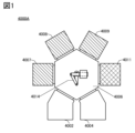
- FIG. 1 is a plan view showing an example of a manufacturing apparatus.
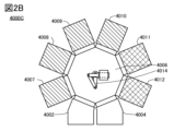
- 2A and 2B are plan views showing an example of a manufacturing apparatus.
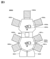
- FIG. 3 is a plan view showing an example of a manufacturing apparatus.
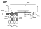
- 4A and 4B are cross-sectional views showing an example of a manufacturing apparatus.
- 5A to 5C are cross-sectional views showing an example of a manufacturing apparatus.
- FIG. 6 is a cross-sectional view showing an example of a manufacturing apparatus.
- 7A to 7D are cross-sectional views illustrating a method for forming a metal oxide film according to one embodiment of the present invention.
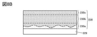
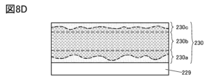
- 8A to 8D are cross-sectional views illustrating a method for forming a metal oxide film according to one embodiment of the present invention.
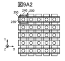
- FIG. 9A1 and 9A2 are plan views showing an example of a semiconductor device
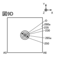
- Fig. 9B to Fig. 9E are cross-sectional views showing an example of a semiconductor device
- 10A to 10C are cross-sectional views showing an example of a semiconductor device
- 11A and 11B are cross-sectional views showing an example of a semiconductor device
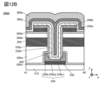
- 12A and 12B are cross-sectional views showing an example of a semiconductor device
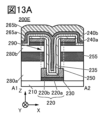
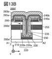
- 13A to 13D are cross-sectional views showing an example of a semiconductor device
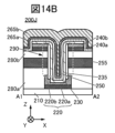
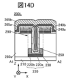
- 14A to 14D are cross-sectional views showing an example of a semiconductor device.
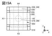
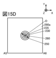
- Fig. 15A is a plan view showing an example of a semiconductor device
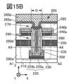
- Figs. 15B to 15E are cross-sectional views showing an example of the semiconductor device.
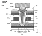
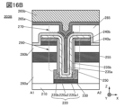
- 16A and 16B are cross-sectional views showing an example of a semiconductor device.
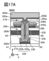
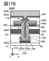
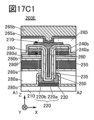
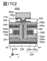
- 17A to 17C2 are cross-sectional views showing an example of a semiconductor device.
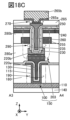
- Fig. 18A is a plan view showing an example of a storage device
- Figs. 18B and 18C are cross-sectional views showing an example of the storage device.
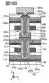
- 19A and 19B are cross-sectional views showing an example of a memory device.
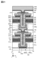
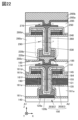
- 20A and 20B are cross-sectional views showing an example of a memory device.
- FIG. 21 is a cross-sectional view showing an example of a storage device.
- FIG. 22 is a cross-sectional view showing an example of a storage device.
- FIG. 23 is a cross-sectional view showing an example of a storage device.
- FIG. 21 is a cross-sectional view showing an example of a storage device.
- FIG. 22 is a cross-sectional view showing an example of a storage device.
- FIG. 23 is a cross-sectional
- FIG. 24 is a cross-sectional view showing an example of a storage device.
- FIG. 25 is a cross-sectional view showing an example of a storage device.
- FIG. 26 is a cross-sectional view showing an example of a storage device.
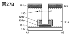
- 27A to 27D are cross-sectional views showing an example of a method for manufacturing a semiconductor device.
- 28A and 28B are cross-sectional views showing an example of a method for manufacturing a semiconductor device.
- 29A and 29B are cross-sectional views showing an example of a method for manufacturing a semiconductor device.
- 30A and 30B are cross-sectional views showing an example of a method for manufacturing a semiconductor device.
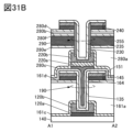
- 31A and 31B are cross-sectional views showing an example of a method for manufacturing a semiconductor device.
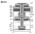
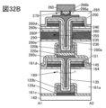
- FIG. 32A and 32B are cross-sectional views showing an example of a method for manufacturing a semiconductor device.
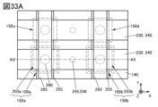
- 33A is a plan view of an example of a storage device
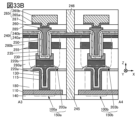
- FIG 33B is a cross-sectional view of the example of the storage device.
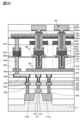
- FIG. 34 is a cross-sectional view showing an example of a storage device.
- FIG. 35 is a cross-sectional view showing an example of a storage device.
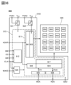
- FIG. 36 is a block diagram illustrating a configuration example of a semiconductor device.
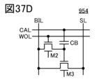
- 37A to 37H are diagrams for explaining examples of the circuit configuration of a memory cell.
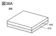
- 38A and 38B are perspective views illustrating a configuration example of a semiconductor device.
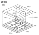
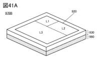
- 41A and 41B are perspective views of a semiconductor device.
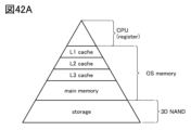
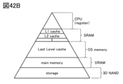
- 42A and 42B are diagrams showing various storage devices by hierarchical level.
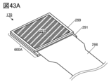
- 43A and 43B are perspective views showing an example of a display device.
- FIG. 44 is a cross-sectional view showing an example of a display device.
- FIG. 45 is a cross-sectional view showing an example of a display device.
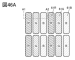
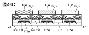
- 46A to 46C are diagrams showing configuration examples of a display device.
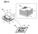
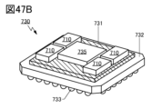
- 47A and 47B are diagrams showing an example of an electronic component.
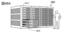
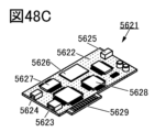
- Fig. 48A to Fig. 48C are diagrams showing an example of a mainframe computer
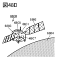
- Fig. 48D is a diagram showing an example of space equipment, and
- Fig. 48E is a diagram showing an example of a storage system applicable to a data center.
- 49A to 49F are diagrams showing an example of an electronic device.
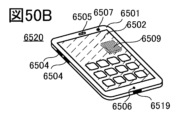
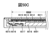
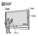
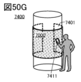
- 50A to 50G are diagrams showing an example of an electronic device.
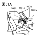
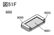
- 51A to 51F are diagrams showing an example of
- ordinal numbers “first” and “second” are used for convenience and do not limit the number of components or the order of the components (e.g., the order of processes or the order of stacking).
- an ordinal number attached to a component in one part of this specification may not match an ordinal number attached to the same component in another part of this specification or in the claims.
- a transistor is a type of semiconductor element that can perform functions such as amplifying current or voltage and switching operations that control conduction or non-conduction.
- transistor includes an IGFET (Insulated Gate Field Effect Transistor) and a thin film transistor (TFT).
- a transistor using an oxide semiconductor or a metal oxide in a semiconductor layer and a transistor having an oxide semiconductor or a metal oxide in a channel formation region may be referred to as an OS transistor.
- a transistor having silicon in a channel formation region may be referred to as a Si transistor.
- a transistor is an element having at least three terminals including a gate, a drain, and a source.
- a transistor has a region (also called a channel formation region) where a channel is formed between the drain (drain terminal, drain region, or drain electrode) and the source (source terminal, source region, or source electrode), and a current can flow between the source and drain through the channel formation region.
- a channel formation region refers to a region through which a current mainly flows.
- source and drain may be interchanged when transistors of different polarity are used, or when the direction of current changes during circuit operation. For this reason, in this specification, the terms “source” and “drain” may be used interchangeably.
- the impurity of a semiconductor refers to, for example, anything other than the main component constituting the semiconductor.
- an element with a concentration of less than 0.1 atomic % can be said to be an impurity.
- the defect level density of the semiconductor may increase or the crystallinity may decrease.
- the semiconductor is an oxide semiconductor
- examples of the impurity that changes the characteristics of the semiconductor include, for example, a Group 1 element, a Group 2 element, a Group 13 element, a Group 14 element, a Group 15 element, and a transition metal other than the main component of the oxide semiconductor.
- Specific examples of the impurity include, for example, hydrogen, lithium, sodium, silicon, boron, phosphorus, carbon, and nitrogen.
- water may also function as an impurity.
- oxygen vacancies also referred to as V O
- V O oxygen vacancies
- an oxynitride refers to a material whose composition contains more oxygen than nitrogen.
- An oxynitride refers to a material whose composition contains more nitrogen than oxygen.
- SIMS secondary ion mass spectrometry
- XPS X-ray photoelectron spectroscopy
- SIMS is suitable when the content of the target element is high (e.g., 0.5 atomic% or more, or 1 atomic% or more).
- SIMS is suitable when the content of the target element is low (e.g., 0.5 atomic% or less, or 1 atomic% or less).
- film and “layer” can be interchanged depending on the circumstances.
- conductive layer can be changed to the term “conductive film.”
- insulating film can be changed to the term “insulating layer.”
- parallel refers to a state in which two straight lines are arranged at an angle of -10 degrees or more and 10 degrees or less. Therefore, it also includes cases in which the angle is -5 degrees or more and 5 degrees or less.
- approximately parallel refers to a state in which two straight lines are arranged at an angle of -20 degrees or more and 20 degrees or less.
- Perfect refers to a state in which two straight lines are arranged at an angle of 80 degrees or more and 100 degrees or less. Therefore, it also includes cases in which the angle is 85 degrees or more and 95 degrees or less.
- approximately perpendicular refers to a state in which two straight lines are arranged at an angle of 70 degrees or more and 110 degrees or less.
- electrically connected includes cases where the connection is made via "something that has some kind of electrical action.”
- something that has some kind of electrical action is not particularly limited as long as it allows the transmission and reception of electrical signals between the connected objects.
- something that has some kind of electrical action includes electrodes or wiring, as well as switching elements such as transistors, resistive elements, coils, and other elements with various functions.
- the off-state current refers to leakage current between the source and drain when a transistor is in an off state (also referred to as a non-conducting state or a cut-off state).
- the off state refers to a state in which the voltage Vgs between the gate and source of an n-channel transistor is lower than the threshold voltage Vth (higher than Vth for a p-channel transistor).
- normally on refers to a state in which a channel exists and current flows through the transistor even when no voltage is applied to the gate.
- Normally off refers to a state in which no current flows through the transistor when no potential is applied to the gate or when a ground potential is applied to the gate.
- a tapered shape refers to a shape in which at least a part of the side of the structure is inclined with respect to the substrate surface or the surface to be formed.
- the side of the structure, the substrate surface, and the surface to be formed do not necessarily need to be completely flat, and may be approximately planar with a slight curvature, or approximately planar with fine irregularities.
- A when it is stated that A is located on B, at least a part of A is located on B. Therefore, for example, it can be rephrased as A has an area located on B.
- a contacts B or A overlaps B when it is stated that A contacts B or A overlaps B, at least a part of A contacts B or overlaps B. Therefore, it can be rephrased as A has an area contacting B or A has an area overlapping B, respectively.
- a covers B at least a part of A covers B. Therefore, for example, it can be rephrased as A has an area covering B.
- a device fabricated using a metal mask or an FMM may be referred to as a device with an MM (metal mask) structure.
- a device fabricated without using a metal mask or an FMM may be referred to as a device with an MML (metal maskless) structure.
- SBS Side By Side
- the SBS structure allows the materials and configuration to be optimized for each light-emitting element, which increases the freedom to select materials and configurations and makes it easier to improve brightness and reliability.
- holes or electrons may be referred to as "carriers".
- a hole injection layer or an electron injection layer may be referred to as a "carrier injection layer”
- a hole transport layer or an electron transport layer may be referred to as a “carrier transport layer”
- a hole block layer or an electron block layer may be referred to as a “carrier block layer”.
- carrier injection layer, carrier transport layer, and carrier block layer may not be clearly distinguishable.
- one layer may have two or three functions among the carrier injection layer, carrier transport layer, and carrier block layer.
- the light-emitting element has an EL layer between a pair of electrodes.
- the EL layer has at least a light-emitting layer.
- the layers (also called functional layers) that the EL layer has include a light-emitting layer, a carrier injection layer (a hole injection layer and an electron injection layer), a carrier transport layer (a hole transport layer and an electron transport layer), and a carrier block layer (a hole block layer and an electron block layer).
- one of the pair of electrodes may be referred to as a pixel electrode, and the other as a common electrode.
- the sacrificial layer (which may also be referred to as a mask layer) is located at least above the light-emitting layer (more specifically, the layer that is processed into an island shape among the layers that make up the EL layer) and has the function of protecting the light-emitting layer during the manufacturing process.
- step discontinuity refers to the phenomenon in which a layer, film, or electrode is divided due to the shape of the surface on which it is formed (e.g., a step, etc.).
- arrows indicating the X direction, Y direction, and Z direction may be used.
- the "X direction” is the direction along the X axis, and the forward direction and the reverse direction may not be distinguished unless explicitly stated.
- the X direction, Y direction, and Z direction are directions that intersect with each other.
- the X direction, Y direction, and Z direction are directions that are perpendicular to each other.
- the manufacturing apparatus of one embodiment of the present invention can perform film formation by two or more film formation methods without exposing the substrate to the atmosphere.
- a plurality of films can be formed by different film formation methods without exposing the substrate to the atmosphere. Therefore, it is possible to significantly reduce the inclusion of impurities during the manufacturing process and to improve the reliability of the transistor, the semiconductor device, the display device, or the memory device.
- impurities such as hydrogen and water in a layer constituting the transistor.
- a manufacturing apparatus has the function of performing at least one of film formation using a sputtering method, film formation using an atomic layer deposition (ALD: Atomic Layer Deposition) method, and film formation using a chemical vapor deposition (CVD: Chemical Vapor Deposition) method.
- ALD Atomic Layer Deposition
- CVD Chemical Vapor Deposition
- RF sputtering which uses a high-frequency power supply as the sputtering power source
- DC sputtering which uses a direct current power supply
- pulsed DC sputtering which changes the voltage applied to the electrodes in a pulsed manner.
- RF sputtering is mainly used when depositing insulating films
- DC sputtering is mainly used when depositing metal conductive films.
- Pulsed DC sputtering is mainly used when depositing compounds such as oxides, nitrides, and carbides using reactive sputtering.
- Examples of the ALD method include the Thermal ALD method, in which the reaction between the precursor and reactant is carried out using only thermal energy, and the Plasma Enhanced ALD (PEALD) method, in which a plasma-excited reactant is used.
- Thermal ALD method in which the reaction between the precursor and reactant is carried out using only thermal energy
- PEALD Plasma Enhanced ALD
- the ALD method can deposit atoms one layer at a time, and therefore has the following advantages: extremely thin films can be formed; films can be formed on structures with high aspect ratios or surfaces with large steps; films can be formed with few defects such as pinholes; films can be formed with excellent coverage; and films can be formed at low temperatures.
- the PEALD method may be preferable because it uses plasma, which allows films to be formed at lower temperatures.
- some precursors used in the ALD method contain elements such as carbon or chlorine.
- films formed by the ALD method may contain more elements such as carbon or chlorine than films formed by other film formation methods.
- the amount of these elements can be quantified using XPS or SIMS. Note that by adopting a condition in which the substrate temperature is high during film formation and/or by carrying out an impurity removal process, the amount of carbon and chlorine contained in the film may be reduced compared to when the ALD method is used without applying these.
- the ALD method differs from other film-forming methods in that particles released from a target or the like are deposited, in that a film is formed by a reaction on the surface of the workpiece. Therefore, it is a film-forming method that is less affected by the shape of the workpiece and has good step coverage.
- the ALD method has excellent step coverage and excellent thickness uniformity, making it suitable for coating the surface of an opening with a high aspect ratio.
- CVD methods can also be classified into plasma CVD (PECVD) methods, which use plasma, thermal CVD (TCVD: Thermal CVD) methods, which use heat, and photo CVD (Photo CVD) methods, which use light. They can also be further classified into metal CVD (MCVD: Metal CVD) methods and metal organic CVD (MOCVD: Metal CVD) methods, depending on the source gas used.
- PECVD plasma CVD
- TCVD Thermal CVD
- Photo CVD Photo CVD
- MCVD Metal CVD
- MOCVD Metal CVD
- the plasma CVD method can produce high-quality films at relatively low temperatures.
- the thermal CVD method is a film formation method that can reduce plasma damage to the workpiece because it does not use plasma.
- no plasma damage occurs during film formation, so films with fewer defects can be obtained.
- a manufacturing apparatus has a first film formation chamber, a second film formation chamber, a third film formation chamber, a first processing chamber, and a transfer chamber.
- the first film formation chamber has a function of forming a film by a thermal ALD method using a first precursor and a first oxidizing agent
- the second film formation chamber has a function of forming a film by a PEALD method using a second precursor and a second oxidizing agent
- the third film formation chamber has a function of forming a film by a thermal ALD method using a third precursor and a third oxidizing agent
- the first processing chamber has a function of performing a heating process or a microwave process
- the first film formation chamber is connected to the second film formation chamber, the third film formation chamber, and the first processing chamber, respectively, via a transfer chamber.
- the film formation process by the thermal ALD method and the film formation process by the PEALD method can be carried out consecutively without exposing the substrate to the atmosphere. Furthermore, even if a heating process or microwave process is carried out between the two film formation processes, this can be carried out within the first processing chamber, which is preferable since there is no need to take the substrate out of the manufacturing apparatus.
- an aluminum oxide film can be formed using a thermal ALD method
- a silicon oxide film can be formed using a PEALD method
- a hafnium oxide film can be formed using a thermal ALD method.
- This three-layer stack structure is suitable for, for example, the gate insulation layer of a transistor.
- a fourth deposition chamber having a function of depositing a conductive layer by a CVD method.
- the fourth deposition chamber is connected to the first deposition chamber, the second deposition chamber, and the first processing chamber, respectively, via the transfer chamber.
- the film formation process using the thermal ALD method, the film formation process using the PEALD method, and the film formation process using the CVD method can be carried out continuously without exposing the substrate to the atmosphere.
- a gate insulating layer in the first to third deposition chambers, and then to continuously form a conductive layer that will become a gate electrode in the fourth deposition chamber.
- a manufacturing apparatus has three film formation chambers, two of which have the function of forming a film by the ALD method, and the remaining film formation chamber has the function of forming a film by the sputtering method, and further, the manufacturing apparatus has a processing chamber that performs a heat treatment, and the processing chamber is connected to each of the three film formation chambers via a transfer chamber.
- the film formation process by the ALD method and the film formation process by the sputtering method can be performed consecutively without exposing the substrate to the atmosphere.
- a manufacturing apparatus with such a configuration is suitable for forming an oxide semiconductor layer, for example, as exemplified in embodiment 2.
- a manufacturing apparatus has a first film formation chamber, a second film formation chamber, a first processing chamber, and a transfer chamber.
- the first film formation chamber has a function of forming a film by the PEALD method using a first precursor and a first gas containing nitrogen
- the second film formation chamber has a function of forming a film by the thermal ALD method using a second precursor and an oxidizing agent
- the first processing chamber has a function of performing a heating process or a microwave process
- the first film formation chamber is connected to the second film formation chamber and the first processing chamber via a transfer chamber.
- the above manufacturing apparatus preferably further includes a third deposition chamber having a function of forming a film by the PEALD method using a third precursor and a second gas containing nitrogen.
- the third deposition chamber is connected to the first deposition chamber, the second deposition chamber, and the first processing chamber, respectively, via a transfer chamber.
- the process of forming a nitride film by PEALD and the process of forming an oxide film by thermal ALD can be performed consecutively without exposing the substrate to the atmosphere.
- a heating process or microwave process is performed between the two film formation processes, it can be performed in the first processing chamber, so there is no need to take the substrate outside the manufacturing apparatus, which is preferable.
- a silicon nitride film can be formed using the PEALD method, and a silicon oxide film can be formed using the thermal ALD method.
- Continuous deposition of an oxide film and a nitride film is suitable for, for example, continuous deposition of a gate insulating layer of a transistor, and continuous deposition of an interlayer film that constitutes a semiconductor device, etc.
- each of the above manufacturing devices preferably further includes a second processing chamber.
- the first processing chamber has a function of performing heat treatment
- the second processing chamber has a function of performing microwave treatment
- the second processing chamber is connected to the first film formation chamber, the second film formation chamber, and the first processing chamber, respectively, via a transfer chamber.
- both heat treatment and microwave treatment are performed between two film formation processes, they can be performed in the first and second treatment chambers, which is preferable since there is no need to take the substrate outside the manufacturing apparatus. Also, even when heat treatment or microwave treatment is performed before or after the film formation process, the first or second treatment chamber can be used, which is preferable.
- FIG. 1 is a schematic diagram of a multi-chamber manufacturing apparatus 4000A.
- FIG. 2A is a schematic diagram of a multi-chamber manufacturing apparatus 4000B.
- FIG. 2B is a schematic diagram of a multi-chamber manufacturing apparatus 4000C.
- FIG. 3 is a schematic diagram of a multi-chamber manufacturing apparatus 4000D.
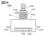
- FIGS. 4A, 4B, and 5A to 5C are cross-sectional views of an ALD apparatus that can be used in the above manufacturing apparatus.
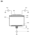
- FIG. 6 is a cross-sectional view of a sputtering apparatus that can be used in the above manufacturing apparatus. Note that FIGS. 1 to 6 show representative configurations, and some configurations are omitted.
- the manufacturing apparatus 4000A has a loading/unloading chamber 4002, a loading/unloading chamber 4004, a transfer chamber 4006, a film formation chamber 4007, a film formation chamber 4008, a film formation chamber 4009, and a processing chamber 4011.
- the loading/unloading chamber 4002 and the loading/unloading chamber 4004 have a function of switching the pressure in the chamber from atmospheric pressure to reduced pressure or from reduced pressure to atmospheric pressure, and can load or unload a substrate.
- the transfer chamber 4006 is provided with a transfer arm 4014, and can transfer a substrate to each chamber in a vacuum.
- the loading/unloading chamber 4002, the loading/unloading chamber 4004, the film-forming chamber 4007, the film-forming chamber 4008, the film-forming chamber 4009, and the processing chamber 4011 are each connected to the transfer chamber 4006 via a gate valve. Therefore, the manufacturing apparatus 4000A can independently maintain the vacuum state of each chamber. This allows continuous processing to be performed in the film-forming chamber 4007, the film-forming chamber 4008, the film-forming chamber 4009, and the processing chamber 4011 without exposing them to the atmosphere, and prevents impurities from being mixed into the film. In addition, contamination of the interface between the substrate and the film and the interface between each film is reduced, and clean interfaces are obtained.
- the difference in pressure between the transport chamber and the film formation chamber is preferably 200 Pa or less, more preferably 100 Pa or less, and even more preferably 50 Pa or less.
- the pressure in the film formation chamber is lower than the pressure in the transport chamber.
- the film formation chambers 4007 to 4009 each have their own film formation apparatus.
- the film formation apparatus include an ALD apparatus, a CVD apparatus, and a sputtering apparatus.
- Examples of the ALD apparatus include a thermal ALD apparatus and a PEALD apparatus.
- Examples of the CVD apparatus include a PECVD apparatus, a thermal CVD apparatus, a photo-CVD apparatus, a metal CVD apparatus, and a MOCVD apparatus.
- the deposition chamber 4007 and deposition chamber 4009 have a thermal ALD device, and the deposition chamber 4008 has a PEALD device.
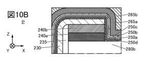
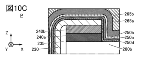
- the formation of the insulating layer 250d, the insulating layer 250a, and the insulating layer 250b (FIG. 10C) described in the third embodiment can be performed in the manufacturing apparatus 4000A.
- the formation of the insulating layer 250d can be performed using a thermal ALD method in the film formation chamber 4007.
- the formation of the insulating layer 250a can be performed using a PEALD method in the film formation chamber 4008.
- the formation of the insulating layer 250b can be performed using a thermal ALD method in the film formation chamber 4009.
- the insulating layer 250d, the insulating layer 250a, and the insulating layer 250b preferably have a low impurity concentration because they function as gate insulating layers. This can prevent impurities from being mixed into the channel formation region of the oxide semiconductor layer.
- the deposition chamber 4007 and deposition chamber 4009 have an ALD device, and the deposition chamber 4008 has a sputtering device.
- a heating device (typically, a vacuum heating device) can be used in the processing chamber 4011.
- the processing chamber 4011 can also be configured to include a processing device other than a film formation device, such as a plasma generation device (typically, a microwave processing device).
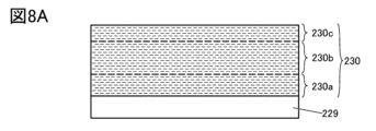
- the oxide semiconductor 230a described in Embodiment 2 ( FIG. 7A ) can be formed in the deposition chamber 4007 by an ALD method.
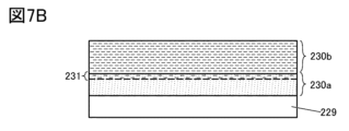
- the oxide semiconductor 230b FIG. 7B
- the oxide semiconductor 230c FIG. 7C
- heat treatment ( FIG. 7D ) is preferably performed in the treatment chamber 4011.
- the oxide semiconductors 230a to 230c can be successively formed and processed without being exposed to the air. This can prevent impurities from being mixed into the formed oxide semiconductor layer 230. In addition, the crystallinity can be improved because the inhibition of crystal growth caused by impurities is suppressed.
- the crystallinity of the oxide semiconductor layer By increasing the crystallinity of the oxide semiconductor layer, it is expected that the increase in electrical resistance of the oxide semiconductor layer can be suppressed or the initial characteristics (particularly the on-state current) of the transistor can be improved, making the transistor suitable for high-speed operation. In addition, the reliability of the transistor can be improved.
- the deposition chamber 4007 and the deposition chamber 4009 have a PEALD device, and the deposition chamber 4008 has a sputtering device.
- the formation of the insulating layer 161c, the insulating layer 161a, and the insulating layer 161d (FIG. 27A) described in the fourth embodiment can be performed in the manufacturing apparatus 4000A.
- the insulating layer 161c can be formed by the PEALD method in the film formation chamber 4007.
- the insulating layer 161a can be formed by the sputtering method in the film formation chamber 4008.
- the insulating layer 161d can be formed by the PEALD method in the film formation chamber 4009.
- the insulating layers 161c, 161a, and 161d can be successively formed without exposure to the air. Therefore, impurities can be prevented from being mixed into the insulating layers 161c, 161a, and 161d.
- the insulating layers 161c, 161a, and 161d are preferably low in impurity concentration because they are in contact with the oxide semiconductor layer or located near the oxide semiconductor layer. This can prevent impurities from being mixed into the channel formation region of the oxide semiconductor layer.
- the insulating layers 280c, 280a, and 280e ( FIG. 28B ) described in embodiment 4 can also be successively formed without exposure to the air.
- the insulating layers 280f, 280b, and 280d ( FIG. 29A ) described in embodiment 4 can also be successively formed without exposure to the air. This can prevent impurities from being mixed into the insulating layers 280a to 280f.
- the insulating layers 280a to 280f are layers in contact with the oxide semiconductor layer or layers located near the oxide semiconductor layer, and therefore preferably have low impurity concentrations. This can prevent impurities from being mixed into the channel formation region of the oxide semiconductor layer.
- the loading/unloading chamber 4002, the loading/unloading chamber 4004, the transfer chamber 4006, the film-forming chamber 4007, the film-forming chamber 4008, the film-forming chamber 4009, and the processing chamber 4011 are each connected to an exhaust means.
- the exhaust means include vacuum pumps such as dry pumps, mechanical booster pumps, cryopumps, and turbomolecular pumps.
- the film-forming chambers 4007, 4008, 4009, and the processing chambers 4011 can be connected to turbomolecular pumps and dry pumps.
- the film-forming chambers 4007, 4008, 4009, and the processing chambers 4011 may be further configured to be provided with cryotraps.
- a dry pump and a powder adsorption trap may be provided.
- a cryopump and a dry pump can be connected to the load/unload chamber 4002, the load/unload chamber 4004, and the transfer chamber 4006.
- the deposition chamber 4007, the deposition chamber 4008, the deposition chamber 4009, and the processing chamber 4011 may be connected to a gas purification device via a gas supply device.
- each chamber may be connected to a gas supply device via a gas heating mechanism.
- the gas heating mechanism is connected to the gas purification device via a gas supply device.
- the gas introduced into the processing chamber may have a dew point of -80°C or less, preferably -100°C or less, and more preferably -120°C or less.
- oxygen gas, nitrogen gas, and noble gas such as argon gas
- the gas introduced into the processing chamber can be heated to 40°C or more and 400°C or less by the gas heating mechanism. It is preferable to provide as many gas heating mechanisms, gas supply devices, and gas purification devices as there are gas types.
- the loading/unloading chamber 4004 the transfer chamber 4006, the film-forming chamber 4007, the film-forming chamber 4008, the film-forming chamber 4009, and the processing chamber 4011, it is preferable to fill them with an inert gas (such as nitrogen gas) with a controlled dew point, and it is desirable to maintain a reduced pressure.
- an inert gas such as nitrogen gas
- a substrate supply chamber can be provided outside the loading/unloading chamber 4002 and the loading/unloading chamber 4004.
- the substrate supply chamber has a cassette port for accommodating substrates and an alignment port for aligning the substrates.
- the substrate supply chamber can be connected to the loading/unloading chamber 4002 and the loading/unloading chamber 4004 by a transfer chamber having a transfer arm. With this configuration, substrates can be transferred between the substrate supply chamber and the loading/unloading chamber 4002 and the loading/unloading chamber 4004.
- the manufacturing apparatus 4000A is configured to have a loading/unloading chamber 4002, a loading/unloading chamber 4004, a film forming chamber 4007, a film forming chamber 4008, a film forming chamber 4009, and a processing chamber 4011, but the present invention is not limited to this.
- the manufacturing apparatus may be configured to have two or four or more film forming chambers.
- the manufacturing apparatus may be configured to have two or more processing chambers.
- the manufacturing apparatus may be configured to have one loading/unloading chamber, or three or more.
- the manufacturing apparatus may be configured to have two or more transport chambers.
- one transport arm 4014 is shown in FIG. 1, the present invention is not limited to this.
- the transport chamber 4006 may be configured to have two or more transport arms.
- the manufacturing apparatus 4000B shown in FIG. 2A differs from the manufacturing apparatus 4000A in that it does not have a film formation chamber 4009.
- the deposition process for multiple layers formed using the same material and the same deposition method may be performed in one deposition chamber.
- the same material here, silicon nitride
- both the process for insulating layer 161c and the process for insulating layer 161d may be performed in one deposition chamber.
- the manufacturing apparatus 4000C shown in FIG. 2B also differs from the manufacturing apparatus 4000A in that it has a film formation chamber 4010 and a processing chamber 4012.
- the deposition chambers 4007 and 4009 have thermal ALD devices, and the deposition chambers 4008 and 4010 have PEALD devices.
- the formation of the insulating layer 250d, the insulating layer 250a, the insulating layer 250b, and the insulating layer 250c (FIG. 10B) described in the third embodiment can be performed in the manufacturing apparatus 4000C.
- the formation of the insulating layer 250d can be performed using a thermal ALD method in the film formation chamber 4007.
- the formation of the insulating layer 250a can be performed using a PEALD method in the film formation chamber 4008.
- the formation of the insulating layer 250b can be performed using a thermal ALD method in the film formation chamber 4009.
- the formation of the insulating layer 250c can be performed using a PEALD method in the film formation chamber 4010.
- an aluminum oxide film for the insulating layer 250d a silicon oxide film for the insulating layer 250a, a hafnium oxide film for the insulating layer 250b, and a silicon nitride film for the insulating layer 250c.
- the insulating layers 250d, 250a, 250b, and 250c preferably have a low impurity concentration because they function as gate insulating layers. This can prevent impurities from being mixed into the channel formation region of the oxide semiconductor layer.
- one of the processing chambers 4011 and 4012 has a heating device (typically, a vacuum heating device) and the other has a plasma generating device (typically, a microwave processing device). This allows both heating and microwave processing to be performed on the film, thereby further reducing the impurity concentration in the film.
- a heating device typically, a vacuum heating device
- a plasma generating device typically, a microwave processing device
- both the processing chamber 4011 and the processing chamber 4012 may have a heating device.
- the processing amount per unit time can be increased for a heat treatment process that has a relatively long processing time. Therefore, the productivity of semiconductor devices and the like can be improved.
- both the processing chamber 4011 and the processing chamber 4012 may have a plasma generation device.
- processing performed in one or both of the processing chambers 4011 and 4012 is not limited to heating processing and microwave processing.
- substrate cleaning processing, plasma processing, reverse sputtering processing, etching processing, ashing processing, etc. may be performed.
- a dry etching device may be provided in one or both of the processing chambers 4011 and 4012.
- the manufacturing apparatus 4000D shown in FIG. 3 has a loading/unloading chamber 4052, a loading/unloading chamber 4054, a transport chamber 4056a, a transport chamber 4056b, a transfer chamber 4065, a film forming chamber 4060a, a film forming chamber 4060b, a film forming chamber 4060c, a film forming chamber 4060d, a film forming chamber 4060e, a processing chamber 4061a, and a processing chamber 4061b.
- a transport arm 4064a is provided in the transport chamber 4056a
- a transport arm 4064b is provided in the transport chamber 4056b.
- the loading/unloading chamber 4052, the loading/unloading chamber 4054, the film forming chamber 4060a, the film forming chamber 4060b, the processing chamber 4061a, and the processing chamber 4061b are independently connected to the transport chamber 4056a via gate valves.
- film formation chamber 4060c, film formation chamber 4060d, and film formation chamber 4060e are independently connected to transfer chamber 4056b, each via a gate valve.
- the loading/unloading chamber 4052 corresponds to the loading/unloading chamber 4002
- the loading/unloading chamber 4054 corresponds to the loading/unloading chamber 4004
- the transport chamber 4056a and the transport chamber 4056b correspond to the transport chamber 4006
- the film formation chambers 4060a to 4060e correspond to the film formation chambers 4007 to 4009
- the treatment chambers 4061a and 4061b correspond to the treatment chamber 4011
- the transport arm 4064a and the transport arm 4064b correspond to the transport arm 4014. Therefore, the above description can be referred to for details.
- the transfer chamber 4065 connects the transfer chamber 4056a and the transfer chamber 4056b. Substrates can be transferred between the transfer arm 4064a and the transfer arm 4064b via the transfer chamber 4065. Note that a configuration may be provided in which multiple transfer chambers are provided between the transfer chamber 4056a and the transfer chamber 4056b. Furthermore, when further transfer chambers are to be added, transfer chambers can be provided as appropriate according to the number of transfer chambers.
- ALD devices can be used in film formation chambers 4060a, 4060b, 4060d, and 4060e, and a sputtering device can be used in film formation chamber 4060c.
- the deposition chambers 4060a and 4060c have a thermal ALD device
- the deposition chamber 4060b has a PEALD device
- the deposition chambers 4060d and 4060e have a metal CVD device or MOCVD device.
- the formation of the conductive layer 265a and the conductive layer 265b can also be performed in the manufacturing apparatus 4000D in succession to the formation of the insulating layer 250d, the insulating layer 250a, and the insulating layer 250b (FIG. 10C) described in the third embodiment.
- the formation of the insulating layer 250d can be performed using a thermal ALD method in the film formation chamber 4060a.
- the formation of the insulating layer 250a can be performed using a PEALD method in the film formation chamber 4060b.
- the formation of the insulating layer 250b can be performed using a thermal ALD method in the film formation chamber 4060c.
- the formation of the conductive layer 265a can be performed in the film formation chamber 4060d, and the formation of the conductive layer 265b can be performed in the film formation chamber 4060e.
- the gate insulating layer and the gate electrode can be formed in succession without being exposed to the atmosphere. This reduces impurities at the interface between the gate insulating layer and the gate electrode, thereby improving the electrical characteristics and reliability of the transistor.
- the manufacturing apparatus of one embodiment of the present invention may be of a single-wafer type, or a batch type in which films are formed on multiple substrates at once.
- the thermal ALD apparatus has a film formation chamber (chamber 4520), a raw material supply unit 4521 (raw material supply units 4521a to 4521c), a raw material supply unit 4531, high-speed valves 4522a to 4522d that are introduction amount controllers, a gas supply unit 4532, a raw material inlet 4523, a raw material outlet 4524, and an exhaust unit 4525.
- the raw material inlet 4523 installed in the chamber 4520 is connected to the raw material supply unit 4521a, the raw material supply unit 4521b, the raw material supply unit 4521c, the raw material supply unit 4531, and the gas supply unit 4532 via a supply pipe and a valve, and the raw material outlet 4524 is connected to the exhaust unit 4525 via an exhaust pipe, a valve, a pressure regulator, and a powder adsorption trap.
- the chamber 4520 includes a substrate holder 4526, and the substrate 4530 is placed on the substrate holder 4526.
- the substrate holder 4526 may have a rotation mechanism.
- a heater 4527 is provided on the outer wall of the chamber 4520, and the temperature of the inside of the chamber 4520, the substrate holder 4526, and the surface of the substrate 4530 can be controlled.
- the heater 4527 can control the temperature of the surface of the substrate 4530 to 100°C or higher and 600°C or lower, preferably 100°C or higher and 350°C or lower, more preferably 200°C or higher and lower than the decomposition temperature of the precursor, and the temperature of the heater 4527 itself can be set to 100°C or higher and 600°C or lower.
- a film By forming a film while heating the substrate in such a temperature range, impurities such as hydrogen or carbon contained in the precursor or reactant can be suppressed from remaining in the film.
- impurities such as hydrogen or carbon contained in the precursor or reactant can be suppressed from remaining in the film.
- the metal atoms and oxygen atoms are rearranged at the same time as the above-mentioned impurities are removed, and each oxide layer can be arranged with high order. Therefore, a metal oxide with a highly crystalline layered crystal structure can be formed.
- a heat treatment after the metal oxide film formation can be performed using the heater 4527.
- a raw material gas is formed from a solid raw material or a liquid raw material by a vaporizer or a heating means.
- the raw material supply unit 4521a, the raw material supply unit 4521b, the raw material supply unit 4521c, and the raw material supply unit 4531 may be configured to supply a gaseous raw material gas.
- a metal oxide can be formed by appropriately selecting the raw materials (such as a volatile organometallic compound) used in the raw material supply unit 4521 and the raw material supply unit 4531 and introducing them into the chamber 4520.
- the raw materials such as a volatile organometallic compound
- a precursor containing indium is supplied from raw material supply unit 4521a
- a precursor containing gallium is supplied from raw material supply unit 4521b
- a precursor containing zinc is supplied from raw material supply unit 4521c.
- precursors containing indium include triethylindium, tris(2,2,6,6-tetramethyl-3,5-heptanedionate)indium, cyclopentadienylindium, indium(III) chloride, and (3-(dimethylamino)propyl)dimethylindium.
- precursors containing gallium include trimethylgallium, triethylgallium, tris(dimethylamido)gallium(III), gallium(III) acetylacetonate, tris(2,2,6,6-tetramethyl-3,5-heptanedionate)gallium, dimethylchlorogallium, diethylchlorogallium, and gallium(III) chloride.
- Examples of zinc-containing precursors include dimethylzinc, diethylzinc, zinc bis(2,2,6,6-tetramethyl-3,5-heptanedionate), and zinc chloride.
- oxidizing agents examples include ozone, oxygen, and water.
- the pressure inside the raw material supply unit 4521 is set to a level at which the internal gas flows sufficiently through the piping when the high-speed valve is opened. For this reason, it is preferable to appropriately adjust the temperature of the raw material supply unit 4521. For example, when storing triethylindium in the raw material supply unit 4521a and triethylgallium in the raw material supply unit 4521b, it is preferable to heat the raw material supply units 4521a and 4521b with a heater to keep them warm, since triethylindium and triethylgallium have low vapor pressures.
- the precursors containing indium, gallium, and zinc have a high decomposition temperature.
- the precursor may be an inorganic precursor.
- the gas made from the inorganic precursor may be highly corrosive. Therefore, it is preferable to use a material with high corrosion resistance, such as titanium, for components that come into contact with gas, such as the chamber, piping, and various gas supply units.
- a reactant is supplied from the raw material supply unit 4531.
- an oxidizing agent containing at least one of ozone, oxygen, and water can be used.
- a carrier gas is supplied from the gas supply unit 4532.
- An inert gas such as argon (Ar), helium (He), or nitrogen (N 2 ) can be used as the carrier gas.
- the precursor of the raw material supply unit 4521 and the reactant of the raw material supply unit 4531 are mixed with the carrier gas and introduced into the chamber 4520.
- a piping heater 4534a is provided to cover the piping or valves between the raw material supply unit 4521a, the raw material supply unit 4521b, the raw material supply unit 4521c, the raw material supply unit 4531, and the gas supply unit 4532 and the chamber 4520.
- a piping heater 4534b is provided to cover the piping or valves between the exhaust device 4525 and the chamber 4520.
- the temperature of the piping heater 4534a and the piping heater 4534b can be appropriately set, for example, in the range of room temperature or higher and 300°C or lower.
- precursors with high decomposition temperatures such as inorganic precursors tend to solidify easily, so when such precursors are used, it is preferable to provide a piping heater to cover the piping of the gas introduction system and the gas exhaust system.
- the temperature control of the piping heater 4534a, the piping heater 4534b, and the heater 4527 can be controlled independently. By independently controlling the piping heater 4534a, the piping heater 4534b, and the heater 4527, the temperature of each heater can be controlled individually. However, this is not limited to this, and the temperature control of the piping heater 4534a, the piping heater 4534b, and the heater 4527 may be configured to be linked to each other. In this case, the temperature control can be adjusted collectively, which makes it possible to reduce the cost of the device components, etc.
- the high-speed valves 4522a to 4522d can be precisely controlled in time. This allows the raw material gases supplied from the raw material supply units 4521a, 4521b, 4521c, and 4531 to be controlled and introduced into the chamber 4520.
- the corresponding high-speed valves among the high-speed valves 4522a to 4522c are opened.
- the high-speed valve 4522d is opened.
- the high-speed valves 4522a to 4522d are closed, and only the carrier gas contained in the gas supply unit 4532 is introduced into the chamber 4520.
- the raw material supply unit 4521 and the gas supply unit 4532 are connected via one high-speed valve each, but the present invention is not limited to this.
- the raw material supply unit 4521 and the gas supply unit 4532 may be connected via two high-speed valves each.
- one of the high-speed valves has a function of drawing the carrier gas of the gas supply unit 4532 into the raw material supply unit 4521.
- the other high-speed valve has a function of pushing the gas in which the precursor and the carrier gas are mixed in the raw material supply unit 4521 to the chamber side.
- FIG. 4A shows an example in which three raw material supply units 4521 and one raw material supply unit 4531 are provided, this embodiment is not limited to this. One, two, or four or more raw material supply units 4521 may be provided. Also, two or more raw material supply units 4531 may be provided.
- the heater 4527, the raw material inlet 4523, and the raw material outlet 4524 are arranged at the bottom of the chamber 4520, but the arrangement of these can be set appropriately without being limited to this.
- the inlets of the raw material supply unit 4521a, the raw material supply unit 4521b, the raw material supply unit 4521c, the raw material supply unit 4531, and the gas supply unit 4532 are combined into the raw material inlet 4523, but the arrangement is not limited to this and each may have a different inlet.
- the manufacturing apparatus can be configured to use a PEALD apparatus.
- the PEALD apparatus has a film formation chamber (chamber 4020), a raw material supply unit 4021 (raw material supply units 4021a to 4021c), a raw material supply unit 4031, high-speed valves 4022a to 4022d which are introduction amount controllers, a gas supply unit 4032, a raw material inlet 4023, a raw material inlet 4033, a raw material outlet 4024, and an exhaust device 4025.
- the raw material inlet 4023 and raw material inlet 4033 installed in the chamber 4020 are connected to the raw material supply unit 4021a, raw material supply unit 4021b, raw material supply unit 4021c, raw material supply unit 4031, and gas supply unit 4032 via supply pipes and valves, respectively, and the raw material outlet 4024 is connected to the exhaust device 4025 via an exhaust pipe, a valve, and a pressure regulator.
- a substrate holder 4026 is provided inside the chamber 4020, and a substrate 4030 is placed on the substrate holder 4026.
- a heater 4027 is provided on the outer wall of the chamber, and pipe heaters 4034a and 4034b are provided to cover pipes connected to the chamber.
- the chamber 4020 corresponds to the chamber 4520
- the raw material supply unit 4021 corresponds to the raw material supply unit 4521
- the raw material supply unit 4031 corresponds to the raw material supply unit 4531
- the high-speed valves 4022a to 4022d correspond to the high-speed valves 4522a to 4522d
- the gas supply unit 4032 corresponds to the gas supply unit 4532
- the raw material inlet 4023 corresponds to the raw material inlet 4523
- the raw material outlet 4024 corresponds to the raw material outlet 4524
- the exhaust device 4025 corresponds to the exhaust device 4525
- the substrate holder 4026 corresponds to the substrate holder 4526
- the substrate 4030 corresponds to the substrate 4530
- the heater 4027 corresponds to the heater 4527
- the pipe heater 4034a corresponds to the pipe heater 4534a
- the pipe heater 4034b corresponds to the pipe heater 4534b.
- the PEALD device can perform film formation by the PEALD method in addition to the thermal ALD method by connecting a plasma generator 4028 to the chamber 4020.
- the plasma generator 4028 is preferably an ICP type plasma generator using a coil 4029 connected to a high-frequency power source.
- the high-frequency power source can output power having a frequency of 10 kHz to 100 MHz, preferably 1 MHz to 60 MHz, and more preferably 2 MHz to 60 MHz. For example, it can output power having a frequency of 13.56 MHz.
- the PEALD method can form a film without reducing the film formation rate even at low temperatures, so it is suitable for use in a single-wafer type film formation device with low film formation efficiency.
- the reactant discharged from the raw material supply unit 4031 passes through the plasma generator 4028 and becomes a plasma state.
- the reactant in a plasma state is introduced into the chamber 4020 from the raw material inlet 4033.
- the reactant discharged from the raw material supply unit 4031 may be configured to be mixed with a carrier gas.
- the substrate holder 4526 may also be provided with a mechanism for applying a constant potential or high frequency. Alternatively, the substrate holder 4526 may be floating or grounded.
- the raw material inlet 4033 is located at the top of the chamber 4520, the heater 4027 and the raw material inlet 4023 are located on the side of the chamber 4520, and the raw material outlet 4524 is located at the bottom of the chamber 4520, but this is not limiting and these locations can be set as appropriate.
- FIG. 5A is a schematic diagram showing one embodiment of a PEALD device.
- the PEALD device 4100 is provided with a reaction chamber 4120 and a plasma generation chamber 4111 above the reaction chamber 4120.
- the reaction chamber 4120 can be called a chamber.
- the reaction chamber 4120 and the plasma generation chamber 4111 can be collectively called a chamber.
- the reaction chamber 4120 has a raw material inlet 4123 and a raw material outlet 4124
- the plasma generation chamber 4111 has a raw material inlet 4133.
- a high frequency such as RF or a microwave can be applied by a plasma generation device 4128 to a gas introduced into the plasma generation chamber 4111 to generate a plasma 4131 in the plasma generation chamber 4111.
- a microwave with a frequency of 2.45 GHz is typically used.
- plasma generated by applying such microwaves and a magnetic field is sometimes called ECR (Electron Cyclotron Resonance) plasma.
- the reaction chamber 4120 also has a substrate holder 4126 on which the substrate 4130 is placed.
- the raw material gas introduced from the raw material inlet 4123 is decomposed by heat from a heater provided in the reaction chamber 4120 and deposited on the substrate 4130.
- the raw material gas introduced from the raw material inlet 4133 is turned into a plasma state by the plasma generation device 4128.
- the raw material gas in the plasma state recombines with electrons or other molecules before reaching the surface of the substrate 4130, turns into a radical state, and reaches the substrate 4130.
- An ALD device that uses radicals to form a film in this way is sometimes called a radical ALD (radical-enhanced ALD) device.
- the PEALD device 4100 shows a configuration in which the plasma generation chamber 4111 is provided at the top of the reaction chamber 4120, but this embodiment is not limited to this.
- the plasma generation chamber 4111 may be provided adjacent to the side of the reaction chamber 4120.
- FIG. 5B is a schematic diagram showing one embodiment of a PEALD apparatus.
- the PEALD apparatus 4200 has a chamber 4220.
- the chamber 4220 has an electrode 4213, a raw material outlet 4224, and a substrate holder 4226, and a substrate 4230 is placed on the substrate holder 4226.
- the electrode 4213 has a raw material inlet 4223 and a shower head 4214 that supplies the introduced raw material gas into the chamber 4220.
- a power source 4215 that can apply high frequency power via a capacitor 4217 is connected to the electrode 4213.
- the substrate holder 4226 may be provided with a mechanism for applying a constant potential or high frequency power. Alternatively, the substrate holder 4226 may be floating or grounded.
- the electrode 4213 and the substrate holder 4226 function as an upper electrode and a lower electrode for generating plasma 4231, respectively.
- the raw material gas introduced from the raw material inlet 4223 is decomposed by heat from a heater provided in the chamber 4220 and deposited on the substrate 4230.
- the raw material gas introduced from the raw material inlet 4223 becomes a plasma state between the electrode 4213 and the substrate holder 4226.
- the raw material gas in the plasma state is incident on the substrate 4230 due to a potential difference (also called an ion sheath) generated between the plasma 4231 and the substrate 4230.
- FIG. 5C is a schematic diagram showing one embodiment of a PEALD apparatus different from that of Figure 5B.
- the PEALD apparatus 4300 has a chamber 4320.
- the chamber 4320 has an electrode 4313, a raw material outlet 4324, and a substrate holder 4326, and a substrate 4330 is placed on the substrate holder 4326.
- the electrode 4313 has a raw material inlet 4323 and a shower head 4314 that supplies the introduced raw material gas into the chamber 4320.
- a power source 4315 that can apply high frequency power via a capacitor 4317 is connected to the electrode 4313.
- the substrate holder 4326 may be provided with a mechanism for applying a constant potential or high frequency power. Alternatively, the substrate holder 4326 may be floating or grounded.
- the electrode 4313 and the substrate holder 4326 function as an upper electrode and a lower electrode for generating plasma 4331, respectively.
- the PEALD apparatus 4300 differs from the PEALD apparatus 4200 in that it has a mesh 4319 connected to a power source 4321 capable of applying high frequency through a capacitor 4322 between the electrode 4313 and the substrate holder 4326. By providing the mesh 4319, the plasma 4231 can be separated from the substrate 4130.
- the source gas introduced from the source inlet 4323 is decomposed by heat from a heater provided in the chamber 4320 and deposited on the substrate 4330. Alternatively, the source gas introduced from the source inlet 4323 becomes a plasma state between the electrode 4313 and the substrate holder 4326.
- the charge of the source gas in the plasma state is removed by the mesh 4319, and the source gas reaches the substrate 4130 in an electrically neutral state such as radicals. Therefore, film formation can be performed with suppressed ion incidence and plasma damage.
- the plasma treatment or microwave treatment may be performed using the PEALD apparatus shown in Figures 4B, 5A to 5C.
- the plasma treatment or microwave treatment can be performed without moving to the treatment chamber.
- the sputtering apparatus has a deposition chamber 4602, and has a backing plate 4608 and a substrate holder 4612 in the deposition chamber 4602.
- the backing plate 4608 can be fitted with a target 4610.
- the target 4610 can be appropriately selected from targets that can be used for an oxide semiconductor layer.
- a substrate 4620 is disposed on the substrate holder 4612. As shown in FIG. 6, it is preferable that the target 4610 and the substrate 4620 are disposed facing each other.
- a magnet unit 4606 Outside the deposition chamber 4602, there are a magnet unit 4606, a DC power supply (direct current power supply) 4615 electrically connected to the backing plate 4608, an RF power supply (high frequency power supply) 4618 electrically connected to the backing plate 4608, and an RF power supply (high frequency power supply) 4616 electrically connected to the substrate holder 4612.
- a magnet unit a combination of multiple magnets is called a magnet unit.
- the sputtering apparatus is provided with an exhaust system having a vacuum pump that exhausts the inside of the deposition chamber 4602, and a gas supply system that introduces gas into the deposition chamber 4602. Also, a configuration in which an adhesion prevention plate is placed inside the deposition chamber 4602 may be used.
- Power applied from the RF power supply 4618 or DC power supply 4615 is applied to the target 4610 via the backing plate 4608.
- plasma can be generated by keeping the deposition chamber 4602 in a reduced pressure state.
- a magnet unit 4606 near the target 4610, the electrons in the plasma are confined by the magnetic field of the magnet unit 4606, increasing the probability of collisions between gas molecules and electrons, and a high-density plasma can be obtained.
- the RF power supply 4618 can output power with a frequency of 10 kHz to 100 MHz, preferably 1 MHz to 60 MHz, more preferably 2 MHz to 60 MHz.
- it can be configured to output power with a frequency of 13.56 MHz.
- the plasma can be made denser.
- the RF sputtering method can be performed.
- the target 4610 has high insulating properties, it is preferable to perform the RF sputtering method.
- the DC power supply 4615 may be configured not to apply power. In this case, the DC power supply 4615 may not be provided.
- the power of the DC power supply 4615 may be applied superimposed on the power of the RF power supply 4618.
- RF superimposed DC sputtering can be performed.
- the ionization rate of gas molecules can be improved by applying the power of the DC power supply 4615, and the film formation rate can be improved.
- a configuration may be used in which power is applied from the DC power supply 4615 instead of from the RF power supply 4618, and DC sputtering is performed.
- the conductivity of the target 4610 is high, it is preferable to perform the DC sputtering method.
- a configuration may be used in which the RF power supply 4618 is not provided.
- a configuration may be adopted in which pulsed power is output from the DC power supply 4615 to perform a pulsed DC sputtering method.
- the pulsed DC sputtering method an oxide or nitride film can be formed by reacting oxygen gas or nitrogen gas to form a film.
- the film can be formed while removing the accumulation of electric charge on the target surface that accompanies the improvement in the insulation of the target surface due to the oxidation or nitridation of the target surface. Therefore, by forming a film using the pulsed DC sputtering method, it is possible to form an oxide or nitride film with relatively high insulation properties.
- a configuration may be adopted in which power is further applied from the RF power supply 4616 to the substrate holder 4612. In other words, a bias potential can be applied to the substrate 4620. Note that a configuration may be adopted in which no power is applied from the RF power supply 4616. In this case, a configuration may be adopted in which the RF power supply 4616 is not provided.
- the substrate holder 4612 preferably has a function of heating the substrate 4620.
- the substrate holder 4612 preferably can heat the substrate 4620 to a temperature of, for example, 100° C. or more and 400° C. or less, and more preferably can heat the substrate 4620 to a temperature of 200° C. or more and 300° C. or less.
- the deposition chamber 4602 is electrically connected to a ground potential at the wall surface, etc.
- the substrate 4620 is placed below the deposition chamber 4602 and the target 4610 is placed above the deposition chamber 4602 in a face-up arrangement, but the present invention is not limited to this.
- the target 4610 may be placed below the deposition chamber 4602 and the substrate 4620 may be placed above the deposition chamber 4602 in a face-down arrangement.
- heating device that can be used in the above-mentioned processing chamber.
- the heating mechanism used in the heating device may be, for example, a mechanism that uses a resistance heating element for heating.
- it may be a mechanism that uses heat conduction or heat radiation from a medium such as a heated gas.
- an electric furnace or an RTA device such as an LRTA device or a GRTA device may be used.
- the workpiece is heated by radiation of light (electromagnetic waves) emitted from a lamp such as a halogen lamp, a metal halide lamp, a xenon arc lamp, a carbon arc lamp, a high-pressure sodium lamp, or a high-pressure mercury lamp.
- a lamp such as a halogen lamp, a metal halide lamp, a xenon arc lamp, a carbon arc lamp, a high-pressure sodium lamp, or a high-pressure mercury lamp.
- heat treatment is performed using a high-temperature gas.
- the temperature of the heat treatment by the heating mechanism may be, for example, 100°C or higher and 800°C or lower, preferably 250°C or higher and 650°C or lower, and more preferably 350°C or higher and 550°C or lower. Typically, it can be 400°C ⁇ 25°C (375°C or higher and 425°C or lower).
- the treatment time can be 10 hours or less, or 1 minute or higher and 5 hours or lower, or 1 minute or higher and 2 hours or lower. When an RTA device is used, the treatment time can be, for example, 1 second or higher and 5 minutes or lower.
- the heat treatment is performed in a nitrogen gas or inert gas atmosphere, or in an atmosphere containing 10 ppm or more, 1% or more, or 10% or more of an oxidizing gas.
- the oxygen gas can be about 20%.
- the heat treatment may be performed under reduced pressure.
- the heat treatment may be performed in an atmosphere containing 10 ppm or more, 1% or more, or 10% or more of an oxidizing gas to compensate for the oxygen that has been released.
- the gas used in the heat treatment is highly purified.
- the amount of moisture contained in the gas used in the heat treatment can be 1 ppb or less, preferably 0.1 ppb or less, and more preferably 0.05 ppb or less.
- the flow ratio of nitrogen gas and oxygen gas is set to 4 slm:1 slm, and the treatment is performed for 1 hour at a temperature of 350° C. or more and 550° C. or less.
- This heat treatment can reduce impurities such as water and hydrogen contained in the oxide semiconductor layer. Furthermore, the crystallinity of the oxide semiconductor layer can be improved.
- a heat treatment can be performed in the treatment chamber as appropriate. This is preferable because it reduces impurities contained in the device being fabricated and also increases the purity of the main components in the film.
- the microwave processing device refers to a device having a power source that generates high-density plasma using microwaves, and the microwave processing refers to processing using the microwave processing device.
- the microwave refers to an electromagnetic wave having a frequency of 300 MHz or more and 300 GHz or less.
- the frequency of the microwave processing device is preferably 300 MHz or more and 300 GHz or less, more preferably 2.4 GHz or more and 2.5 GHz or less, and can be, for example, 2.45 GHz.
- high-density plasma high-density oxygen radicals can be generated.
- the power of the power source that applies microwaves to the microwave processing device is preferably 1000 W or more and 10,000 W or less, and preferably 2000 W or more and 5000 W or less.
- the microwave processing device may have a power source that applies high-frequency waves such as RF to the substrate side. Furthermore, by applying high-frequency waves such as RF to the substrate side, oxygen ions generated by high-density plasma can be efficiently guided to the workpiece.
- the microwave treatment is preferably carried out under reduced pressure, with the pressure being preferably 10 Pa or more and 1000 Pa or less, and more preferably 300 Pa or more and 700 Pa or less.
- the treatment temperature is preferably 750° C. or less, more preferably 500° C. or less, and can be, for example, about 250° C.
- a heat treatment may be carried out continuously without exposure to the atmosphere.
- the temperature of the heat treatment is, for example, preferably 100° C. or more and 750° C. or less, and more preferably 300° C. or more and 500° C. or less.
- the microwave treatment can be performed using oxygen gas and argon gas.
- the oxygen flow ratio (O 2 /(O 2 +Ar)) is greater than 0% and less than or equal to 100%.
- the oxygen flow ratio (O 2 /(O 2 +Ar)) is greater than 0% and less than or equal to 50%.
- the oxygen flow ratio (O 2 /(O 2 +Ar)) is greater than or equal to 10% and less than or equal to 40%.
- the oxygen flow ratio (O 2 /(O 2 +Ar)) is greater than or equal to 10% and less than or equal to 30%.
- oxygen gas By performing microwave treatment in an atmosphere containing oxygen, oxygen gas can be turned into plasma using microwaves or high frequency waves such as RF, and the oxygen plasma can be applied to the oxide semiconductor layer.
- VOH in the oxide semiconductor layer By the action of plasma, microwaves, or the like, VOH in the oxide semiconductor layer can be split into oxygen vacancies and hydrogen, and hydrogen, which is an impurity, can be removed from the oxide semiconductor layer.
- hydrogen which is an impurity
- carbon bonded to oxygen, hydrogen, or the like can also be removed in some cases.
- impurities such as carbon or hydrogen can be reduced by performing microwave treatment.
- oxygen radicals generated by the oxygen plasma can be supplied to oxygen vacancies formed in the oxide semiconductor layer, whereby oxygen vacancies in the oxide semiconductor layer can be further reduced.
- Oxygen supplied to the oxide semiconductor layer can be in various forms, such as oxygen atoms, oxygen molecules, oxygen ions, and oxygen radicals (also called O radicals, which are atoms, molecules, or ions having an unpaired electron). Note that oxygen supplied to the oxide semiconductor layer can be in one or more of the above forms, and is particularly preferably in the form of oxygen radicals.
- the impurities in the oxide semiconductor layer can be reduced. This allows crystal growth to be performed in a state where the impurity concentration in the oxide semiconductor layer is reduced, thereby further improving the crystallinity.
- the microwave treatment may be performed after the oxide semiconductor layer is formed, or after an insulating layer (e.g., at least a part of a gate insulating layer) is formed over the oxide semiconductor layer.
- the insulating layer includes an insulating layer (e.g., an aluminum oxide film) having a function of trapping or fixing hydrogen
- the microwave treatment is preferably performed after the insulating layer is formed. In this way, hydrogen generated by the microwave treatment can be trapped or fixed to the insulating layer. Therefore, VOH contained in the channel formation region can be more effectively reduced.
- microwave treatment can be performed in a treatment chamber to improve the film quality and suppress the diffusion of impurities such as hydrogen and water.
- microwave treatment can be performed to improve the film quality of the gate insulating layer, thereby improving the reliability of the transistor.
- the number of times of microwave treatment may be one or more.
- microwave treatment may be performed every time a layer is formed, or microwave treatment may be performed after at least one layer is formed.
- microwave treatment may be performed before forming a gate insulating layer.
- microwave treatment may also serve as heating treatment.
- the oxide semiconductor layer of one embodiment of the present invention preferably includes a metal oxide having crystallinity.
- a metal oxide having crystallinity examples include a c-axis aligned crystal (CAAC) structure, a polycrystalline (poly-crystal) structure, and a nanocrystalline (nc) structure.
- CAAC c-axis aligned crystal
- nc nanocrystalline
- the oxide semiconductor layer of one embodiment of the present invention preferably has a metal oxide having a CAAC structure.
- the CAAC structure is a crystal structure in which a plurality of microcrystals (typically, a plurality of microcrystals having a hexagonal crystal structure) have a c-axis orientation and are connected without being oriented in the a-b plane.
- TEM transmission electron microscope
- the crystallinity of the oxide semiconductor layer can be analyzed, for example, by X-ray diffraction (XRD), TEM, or electron diffraction (ED). Alternatively, the analysis may be performed by combining a plurality of these techniques.
- XRD X-ray diffraction
- TEM TEM
- ED electron diffraction
- the crystallinity of the semiconductor material of the oxide semiconductor layer is not particularly limited.
- the oxide semiconductor layer may contain one or more of an amorphous semiconductor (a semiconductor having an amorphous structure), a single crystal semiconductor (a semiconductor having a single crystal structure), or a semiconductor having crystallinity other than single crystal (a microcrystalline semiconductor, a polycrystalline semiconductor, or a semiconductor having a crystalline region in part).
- an amorphous semiconductor a semiconductor having an amorphous structure
- a single crystal semiconductor a semiconductor having a single crystal structure
- a semiconductor having crystallinity other than single crystal a microcrystalline semiconductor, a polycrystalline semiconductor, or a semiconductor having a crystalline region in part.
- Examples of the metal oxide contained in the oxide semiconductor layer of one embodiment of the present invention include indium oxide, gallium oxide, and zinc oxide.
- the metal oxide according to one embodiment of the present invention preferably contains at least indium (In) or zinc (Zn).
- the metal oxide preferably contains two or three elements selected from indium, element M, and zinc.
- element M is a metal element or semimetal element having a high bond energy with oxygen, for example, a metal element or semimetal element having a bond energy with oxygen higher than that of indium.
- element M examples include aluminum, gallium, tin, yttrium, titanium, vanadium, chromium, manganese, iron, cobalt, nickel, zirconium, molybdenum, hafnium, tantalum, tungsten, lanthanum, cerium, neodymium, magnesium, calcium, strontium, barium, boron, silicon, germanium, and antimony.
- the element M of the metal oxide is preferably one or more of the above elements, more preferably one or more selected from aluminum, gallium, tin, and yttrium, and even more preferably gallium.
- the metal oxide according to one embodiment of the present invention preferably has one or more selected from indium, gallium, and zinc.
- metal elements and metalloid elements may be collectively referred to as “metal elements", and the "metal element” described in this specification may include metalloid elements.
- metal oxides examples include indium zinc oxide (In-Zn oxide), indium tin oxide (In-Sn oxide), indium titanium oxide (In-Ti oxide), indium gallium oxide (In-Ga oxide), indium gallium aluminum oxide (In-Ga-Al oxide), indium gallium tin oxide (In-Ga-Sn oxide, also referred to as IGTO), gallium zinc oxide (Ga-Zn oxide, also referred to as GZO), aluminum zinc oxide (Al-Zn oxide, also referred to as AZO), indium aluminum oxide (In-Ga-Al-Zn oxide, also referred to as IGTO), and indium zinc oxide (In-Ga-Al-Zn oxide, also referred to as IGTO).
- In-Zn oxide indium zinc oxide
- In-Sn oxide indium tin oxide
- In-Ti oxide indium titanium oxide
- In-Ga oxide indium gallium oxide
- In-Ga-Al oxide indium gallium tin oxide
- Indium zinc oxide (In-Al-Zn oxide, also written as IAZO), indium tin zinc oxide (In-Sn-Zn oxide, also written as ITZO (registered trademark)), indium titanium zinc oxide (In-Ti-Zn oxide), indium gallium zinc oxide (In-Ga-Zn oxide, also written as IGZO), indium gallium tin zinc oxide (In-Ga-Sn-Zn oxide, also written as IGZTO), indium gallium aluminum zinc oxide (In-Ga-Al-Zn oxide, also written as IGAZO or IAGZO), etc.
- indium tin oxide containing silicon also called ITSO
- gallium tin oxide Ga-Sn oxide
- aluminum tin oxide Al-Sn oxide
- the transistor By increasing the ratio of the number of indium atoms to the sum of the number of atoms of all metal elements contained in the metal oxide, the transistor can obtain a large on-current and high frequency characteristics.
- the metal oxide may have one or more metal elements having a higher period number in the periodic table instead of indium.
- the metal oxide may have one or more metal elements having a higher period number in the periodic table in addition to indium.
- Examples of metal elements having a higher period number in the periodic table include metal elements belonging to the fifth period and metal elements belonging to the sixth period.
- the metal elements include yttrium, zirconium, silver, cadmium, tin, antimony, barium, lead, bismuth, lanthanum, cerium, praseodymium, neodymium, promethium, samarium, and europium. Note that lanthanum, cerium, praseodymium, neodymium, promethium, samarium, and europium are called light rare earth elements.
- the metal oxide may also contain one or more nonmetallic elements.
- the field effect mobility of the transistor may be increased.
- nonmetallic elements include carbon, nitrogen, phosphorus, sulfur, selenium, fluorine, chlorine, bromine, and hydrogen.
- the metal oxide becomes highly crystalline, and the diffusion of impurities in the metal oxide can be suppressed. Therefore, fluctuations in the electrical characteristics of the transistor can be suppressed, and reliability can be improved.
- the formation of oxygen vacancies in the metal oxide can be suppressed. Therefore, carrier generation due to oxygen vacancies can be suppressed, and a transistor with a small off-current can be obtained. Furthermore, fluctuations in the electrical characteristics of the transistor can be suppressed, and reliability can be improved.
- In-Ga-Zn oxide may be used as an example of a metal oxide.
- the oxide semiconductor layer of one embodiment of the present invention can be manufactured by forming a metal oxide using two types of film formation methods.
- the oxide semiconductor layer of one embodiment of the present invention can be manufactured by forming a metal oxide using a first film formation method and a second film formation method.
- a hybrid OS an oxide semiconductor layer formed using two types of film formation methods may be called a hybrid OS.
- the oxide semiconductor layer of one embodiment of the present invention has crystallinity.
- the oxide semiconductor layer of one embodiment of the present invention preferably has a CAAC structure.
- a metal oxide film having crystallinity is formed by using the first film formation method.
- the metal oxide film formed at this time has a CAAC structure.
- a metal oxide film formed by a sputtering method is likely to have crystallinity.
- a mixed layer may be formed at the interface between the metal oxide and the layer on which it is formed.
- the mixed layer may be formed by particles (also called sputtering particles) emitted from a target or the like, or by energy imparted to the substrate by the sputtering particles or the like. There is a concern that the mixed layer may inhibit the crystallization of the metal oxide.
- silicon oxide when an insulating layer having silicon is used as the surface to be formed, for example silicon oxide, there is a risk that silicon may be mixed into the metal oxide when a metal oxide is formed on the silicon oxide using the first film formation method. There is a concern that the crystallization of the metal oxide may be inhibited due to the mixing of impurities such as silicon into the metal oxide.
- a metal oxide is formed using the second film formation method. That is, after forming a metal oxide as a first layer using the second film formation method, a metal oxide is formed as a second layer on the first layer using the first film formation method. At this time, it is preferable to use a film formation method that causes less damage to the surface to be formed compared to the first film formation method as the second film formation method. By using a film formation method that causes less damage to the surface to be formed as the second film formation method, it is possible to suppress the formation of a mixed layer at the interface between the oxide semiconductor layer and the layer that is the surface to be formed of the oxide semiconductor layer.
- atomic layer deposition ALD
- chemical vapor deposition CVD
- the first layer may be, for example, a metal oxide having a microcrystalline structure or an amorphous structure with lower crystallinity than the CAAC structure.
- the crystallinity of the first layer may be increased with the second layer as a nucleus. This may increase the crystallinity of the entire oxide semiconductor layer, including the vicinity of the interface with the surface on which it is formed.
- the oxide semiconductor layer of one embodiment of the present invention it is preferable to first form a metal oxide on a surface to be formed by using the second film formation method, and then form a metal oxide above the metal oxide by using the first film formation method.
- Examples of the first film formation method include sputtering and pulsed laser deposition (PLD).
- the second film formation method may be, for example, the ALD method, the plasma enhanced CVD (PECVD) method, the thermal CVD method, the photo-CVD method, the metal organic CVD (MOCVD) method, the molecular beam epitaxy (MBE) method, etc.
- the MBE method is a film formation method that grows a thin film with a crystal structure that reflects the crystal system of the substrate, and can be said to be one of the film formation methods that cause less damage to the surface on which the film is formed.
- a wet method can be used as the second film formation method.
- the wet method is one of the film formation methods that cause less damage to the surface on which the film is formed.
- a spray coating method can be used.
- the oxide semiconductor layer of one embodiment of the present invention can be manufactured by forming a metal oxide as a first layer by using the second film formation method, and then forming a metal oxide as a second layer by using the first film formation method.
- an ALD method can be used as the second film formation method
- a sputtering method can be used as the first film formation method.
- the metal oxide formed by using the first film formation method preferably has a CAAC structure.
- a third layer can be formed on the second layer. Since the second layer has high crystallinity, the third layer can grow crystals using the crystals of the second layer as nuclei or seeds. Therefore, even if a film formation method that is likely to have crystallinity is not used as a film formation method for the third layer, the third layer can be crystallized.
- the oxide semiconductor layer can have both high crystallinity and high coverage throughout the layer.
- the oxide semiconductor layer can have high crystallinity throughout the layer.
- the second layer has excellent crystallinity because the effect of the surface on which it is formed is reduced by providing the first layer, which increases its crystallinity. Therefore, it is expected that a layer with excellent crystallinity will also be formed in the third layer, which is crystallized using the second layer as a nucleus or seed.
- the third layer is the top layer of the oxide semiconductor layer, and when the oxide semiconductor layer is used as a semiconductor layer of a transistor, it is, for example, a layer in contact with the gate insulating layer. By increasing the crystallinity of the layer in contact with the gate insulating layer, it is possible to increase carrier mobility when the transistor is in the on state.
- the oxide semiconductor layer of one embodiment of the present invention can be manufactured by forming a metal oxide as a first layer using the second film formation method, forming a metal oxide as a second layer using the first film formation method, and forming a metal oxide as a third layer using the second film formation method.
- the ALD method can be used as the second film formation method
- the sputtering method can be used as the first film formation method.
- the metal oxide formed using the first film formation method preferably has a CAAC structure.
- the ALD method is a film formation method with better coverage than the sputtering method, and the coverage of the oxide semiconductor layer can be improved by using the ALD method as the film formation method for the first layer and the third layer. Therefore, the oxide semiconductor layer can be well covered on steps, openings, and the like with a high aspect ratio.
- the oxide semiconductor layer 230 can be manufactured, for example, by forming an oxide semiconductor 230a on a layer 229 that is a surface to be formed by an ALD method, forming an oxide semiconductor 230b on the oxide semiconductor 230a by a sputtering method, and forming an oxide semiconductor 230c on the oxide semiconductor 230b by an ALD method.
- heat treatment is preferably performed. The heat treatment can improve the crystallinity of the oxide semiconductor layer 230.
- the heat treatment here is not limited to heating treatment. For example, heat applied during a manufacturing process may be used.
- the layer 229 is an insulating film, and is, for example, an insulating film such as a silicon oxide film, a silicon oxynitride film, a silicon nitride film, a silicon nitride oxide film, an aluminum oxide film, or a hafnium oxide film.
- the oxide semiconductor layer 230 can be used as the oxide semiconductor layer 230 included in each transistor described in Embodiment 3.
- the layer 229 corresponds to one or more of the conductive layer 220, the insulating layer 235, the conductive layer 240, and the like described in Embodiment 3.
- Layer 229 does not have to be crystalline. In addition, if layer 229 is crystalline, it may have a crystal structure with low lattice matching with the metal oxide of oxide semiconductor layer 230.
- an oxide semiconductor 230a is formed on the layer 229 (FIG. 7A). Then, an oxide semiconductor 230b is formed on the oxide semiconductor 230a (FIG. 7B).
- the oxide semiconductor 230b is preferably formed by using a sputtering method.
- the oxide semiconductor 230b is preferably made to have a composition suitable for forming a CAAC structure.
- the oxide semiconductor 230a is preferably formed using a deposition method that causes less damage to the surface on which it is formed compared to the deposition method for the oxide semiconductor 230b.
- the oxide semiconductor 230a is formed using the ALD method.
- the oxide semiconductor 230b is formed by a sputtering method.
- the oxide semiconductor 230a is preferably formed by a deposition method that causes little damage to the surface on which it is formed.
- the thickness of the alloyed region can be made thin, or can be made thin enough that the alloyed region cannot be observed.
- the thickness of the alloyed region can be set to 0 nm or more and 3 nm or less, preferably 0 nm or more and 2 nm or less, more preferably 0 nm or more and 1 nm or less, and even more preferably 0 nm or more and less than 0.3 nm.
- Figures 7A and 7B show an example in which no alloyed region is formed between the layer 229 and the oxide semiconductor 230a.
- the thickness of the alloyed region may be calculated by performing a line analysis of the composition of the region and its surroundings using SIMS or Energy Dispersive X-ray Spectroscopy (EDX).
- an EDX line analysis is performed on the above region and its periphery with the direction perpendicular to the surface of the oxide semiconductor 230a being the depth direction.
- the depth at which the quantitative value of a metal (In when the oxide semiconductor 230a contains In) that is the main component of the oxide semiconductor 230a and is not the main component of the layer that will be the surface to be formed (here, layer 229) becomes half-value is defined as the depth (position) of the interface between the above region and the oxide semiconductor 230a.
- the depth at which the quantitative value of an element (e.g., Si) that is the main component of the layer that will be the surface to be formed and is not the main component of the oxide semiconductor 230a becomes half-value is defined as the depth (position) of the interface between the above region and the layer that will be the surface to be formed. From the above, the thickness of the alloyed region can be calculated.
- an element e.g., Si
- the thickness of the alloyed region in the oxide semiconductor layer of one embodiment of the present invention is observed by EDX analysis, the thickness is, for example, 0 nm or more and 3 nm or less, preferably 0 nm or more and 2 nm or less, more preferably 0 nm or more and 1 nm or less, and even more preferably 0 nm or more and less than 0.3 nm.
- the interface is defined as a depth at which the silicon concentration becomes 50% of the maximum concentration of the layer 229, and the distance between the interface and the depth at which the silicon concentration decreases to 1.0 ⁇ 10 21 atoms/cm 3 , preferably 5.0 ⁇ 10 20 atoms/cm 3 , more preferably 1.0 ⁇ 10 20 atoms/cm 3 is defined as thickness t_s2.
- the thickness t_s2 is preferably 3 nm or less, more preferably 2 nm or less.
- the thickness t_s2 can be set to a value within the above range.
- the vicinity of the surface to be formed refers to, for example, a region that is more than 0 nm and not more than 3 nm, preferably more than 0 nm and not more than 2 nm, and more preferably 1 nm or more and not more than 2 nm, approximately perpendicular to the surface to be formed of the oxide semiconductor layer 230.
- the CAAC structure near the surface to be formed may be observed by observation using a TEM.
- a TEM For example, in cross-sectional observation of the oxide semiconductor layer 230 using a high-resolution TEM, bright spots arranged in layers in a direction parallel to the surface to be formed are observed near the surface to be formed.
- the CAAC structure near the surface to be formed may be evaluated from a map showing the crystal orientation.
- the map showing the crystal orientation may be obtained, for example, by acquiring a cross-sectional TEM image, performing a fast Fourier transform (FFT) process on each region in the cross-sectional TEM image to create an FFT pattern, and calculating the direction of the crystal axis of each region.
- the FFT pattern reflects reciprocal lattice space information similar to an electron beam diffraction pattern.
- a region in which the calculated crystal axis direction of each region is 70° or more and 100° or less with respect to the surface to be formed can be considered to be a CAAC structure.
- an oxide semiconductor layer having a microcrystalline structure or an amorphous structure with lower crystallinity than the CAAC structure may be formed. That is, at the manufacturing stage shown in FIG. 7A, the oxide semiconductor 230a may have a region with lower crystallinity than the oxide semiconductor 230b.
- a source gas containing a precursor having indium is introduced into the chamber, and the precursor is adsorbed onto the surface of layer 229.
- the temperature for heating the substrate corresponds to the decomposition temperature of the precursor.
- the introduction of the raw material gas is stopped, the chamber is purged, and excess precursors and reaction products are discharged from the chamber.
- an oxidizing agent is introduced into the chamber as a reactant, and reacted with the adsorbed precursor to form a layer of indium and oxygen (hereinafter, the first layer) by desorbing components other than indium while leaving indium adsorbed to the substrate.
- Ozone, oxygen, water, etc. can be used as the oxidizing agent.
- the introduction of the oxidizing agent is stopped, the chamber is purged, and excess reactants and reaction products are discharged from the chamber.
- a source gas containing a precursor having element M is introduced into the chamber and adsorbed onto the first layer.
- the temperature for heating the substrate corresponds to the decomposition temperature of the precursor.
- the introduction of the raw material gas is stopped, the chamber is purged, and excess precursors and reaction products are discharged from the chamber.
- an oxidizing agent is introduced into the chamber as a reactant, and reacted with the adsorbed precursor, so that components other than element M are desorbed while element M is still adsorbed on the substrate, forming a layer in which element M is combined with oxygen (hereinafter, the second layer).
- the introduction of the oxidizing agent is stopped, the chamber is purged, and excess reactants and reaction products are discharged from the chamber.
- a raw material gas containing a zinc-containing precursor is introduced into the chamber and adsorbed onto the second layer.
- the temperature for heating the substrate corresponds to the decomposition temperature of the precursor.
- the substrate heating temperature is 100°C or higher and 350°C or lower, preferably 150°C or higher and 300°C or lower.
- the introduction of the raw material gas is stopped, the chamber is purged, and excess precursors and reaction products are discharged from the chamber.
- an oxidizing agent is introduced into the chamber as a reactant, and reacted with the adsorbed precursor, leaving zinc adsorbed on the substrate while components other than zinc are desorbed, forming a layer of zinc and oxygen combined (hereinafter, the third layer).
- the introduction of the oxidizing agent is stopped, the chamber is purged, and excess reactants and reaction products are discharged from the chamber.
- the first layer is formed again on the third layer by the method described above.
- In-M-Zn oxide can be formed as the oxide semiconductor 230a on the layer 229 by the ALD method.
- the ALD method can control the composition of the film obtained by adjusting the amount of raw material gas introduced.
- the ALD method can form a film of any composition by adjusting the amount of raw material gas introduced, the number of introductions (also called the number of pulses), the time required for one pulse (also called the pulse time), etc.
- the ALD method can form a film whose composition changes continuously by changing the raw material gas while forming the film.
- the time required for film formation can be shortened compared to when forming a film using multiple film formation chambers because no time is required for transportation and pressure adjustment. Therefore, the productivity of semiconductor devices can be increased in some cases.
- an In-M-Zn oxide is formed as the oxide semiconductor 230b on the oxide semiconductor 230a using the sputtering method.
- the mixed layer 231 is formed on or near the surface of the oxide semiconductor 230a.
- minute crystal regions may be formed in the mixed layer 231 due to sputtering particles or energy provided to the substrate by the sputtering particles when the oxide semiconductor 230b is formed.
- the mixed layer 231 or the minute crystal regions formed in the mixed layer 231 may become nuclei, and at least a part of the oxide semiconductor 230a may crystallize.
- In-M-Zn oxide can be used as a target for the sputtering method.
- oxygen or a mixed gas of oxygen and a noble gas can be used as the sputtering gas.
- the proportion of oxygen contained in the sputtering gas the amount of excess oxygen in the oxide film to be formed can be increased.
- the higher the ratio of the flow rate of oxygen gas to the total deposition gas used during deposition (hereinafter also referred to as the oxygen flow rate ratio), the more crystalline the metal oxide may be formed.
- an oxygen-excess metal oxide may be formed when the ratio of oxygen contained in the sputtering gas is set to more than 30% and not more than 100%, preferably 70% to 100%.
- a transistor using an oxygen-excess oxide semiconductor layer in a channel formation region can have relatively high reliability.
- one embodiment of the present invention is not limited thereto.
- An oxygen-deficient metal oxide is formed when the ratio of oxygen contained in the sputtering gas is set to 1% to 30%, preferably 5% to 20%, when the transistor is formed.
- a relatively high field effect mobility can be obtained when an oxygen-deficient metal oxide is used in a channel formation region.
- the composition of the formed metal oxide may differ from the composition of the sputtering target.
- the zinc content in the formed metal oxide may decrease to about 50% compared to the sputtering target.
- the substrate heating temperature is preferably, for example, 100°C or more and 400°C or less, and more preferably 200°C or more and 300°C or less.
- an oxide semiconductor 230a and an oxide semiconductor 230b on the oxide semiconductor 230a can be formed on the layer 229.
- the oxide semiconductor 230c is formed on the oxide semiconductor 230b (FIG. 7C).
- the oxide semiconductor 230c is formed using the ALD method.
- the formation of the oxide semiconductor 230c using the ALD method can be performed by referring to the method for forming the oxide semiconductor 230a.
- the oxide semiconductor 230c When an oxide semiconductor 230c having a lower crystallinity than the CAAC structure is formed on an oxide semiconductor 230b having a CAAC structure by using an ALD method, the oxide semiconductor 230c may grow epitaxially with the oxide semiconductor 230b as a nucleus. Therefore, when the oxide semiconductor 230c is formed, the oxide semiconductor 230c may have a region having the CAAC structure. In addition, it is preferable that the region having the CAAC structure is formed over the entire oxide semiconductor 230c.
- a heat treatment process may be performed.
- the temperature of the heat treatment is, for example, 100°C to 800°C, preferably 250°C to 650°C, more preferably 350°C to 550°C. Typically, it can be 400°C ⁇ 25°C (375°C to 425°C).
- the treatment time can be 10 hours or less, or 1 minute to 5 hours, or 1 minute to 2 hours. When an RTA apparatus is used, the treatment time can be, for example, 1 second to 5 minutes. It is expected that the heat treatment will repair the gaps in the atomic-level crystal parts of the CAAC structure of the oxide semiconductor 230b by the oxide semiconductor 230c (in other words, the crystal molecules formed by the ALD method).
- the heating device used for the heat treatment is not particularly limited, and may be a device that heats the workpiece by thermal conduction or thermal radiation from a heating element such as a resistance heating element.
- a heating element such as a resistance heating element.
- an electric furnace or an RTA (Rapid Thermal Anneal) device such as an LRTA (Lamp Rapid Thermal Anneal) device or a GRTA (Gas Rapid Thermal Anneal) device can be used.
- An LRTA device is a device that heats the workpiece by radiation of light (electromagnetic waves) emitted from a lamp such as a halogen lamp, metal halide lamp, xenon arc lamp, carbon arc lamp, high pressure sodium lamp, or high pressure mercury lamp.
- a GRTA device is a device that performs heat treatment using high-temperature gas.
- the heat treatment process may increase the crystallinity of the region having the CAAC structure in the oxide semiconductor 230c. Furthermore, if the region is formed only below the oxide semiconductor 230c after film formation by the ALD method, the heat treatment process may cause the region to expand upward (FIG. 7D). In other words, the heat treatment may cause the region having the CAAC structure to be formed throughout the entire layer in the oxide semiconductor 230c.
- this heat treatment process may further repair the oxide semiconductor 230b by the oxide semiconductor 230c (in other words, the crystal molecules formed using the ALD method) that fills the gaps in the atomic-level crystal parts of the CAAC structure of the oxide semiconductor 230b.
- the oxide semiconductor 230a is converted into CAAC by this heat treatment process (FIG. 7D). It is expected that the CAAC conversion is likely to occur because the mixed layer 231 formed in the oxide semiconductor 230a during the deposition of the oxide semiconductor 230b acts as a nucleus or seed. It is preferable that the region in the oxide semiconductor 230a that is converted into CAAC is large, and it is preferable that the CAAC conversion extends to the vicinity of the layer 229.
- the oxide semiconductor 230a is converted into CAAC from the top to the bottom, the CAAC can be converted into CAAC up to the vicinity of the layer 229 without being limited by the material or crystallinity of the layer 229.
- the method for manufacturing an oxide semiconductor layer according to one embodiment of the present invention is particularly suitable for the case where the layer on which the oxide semiconductor layer is to be formed has an amorphous structure.
- microwave treatment is preferably performed in an atmosphere containing oxygen.
- impurities such as hydrogen and carbon in the oxide semiconductor layer 230 can be reduced.
- 7A to 7D are cross-sectional views illustrating a method for forming a metal oxide film according to one embodiment of the present invention.
- 7A to 7D can also be regarded as conceptual diagrams illustrating a model for forming a metal oxide film according to one embodiment of the present invention.
- the oxide semiconductor 230a and the oxide semiconductor 230c each have high crystallinity using the oxide semiconductor 230b, which has high crystallinity, as a nucleus or seed.
- the crystallinity of the oxide semiconductor 230a may be increased by heat treatment during the formation of the oxide semiconductor 230b or after the formation of the oxide semiconductor 230c.
- the crystallinity of the oxide semiconductor 230c may be increased by heat treatment during the formation of the oxide semiconductor 230c or after the formation of the oxide semiconductor 230c.
- the heat treatment has an assisting effect of increasing the crystallinity.
- the highly crystalline oxide semiconductor 230b i.e., CAAC
- CAAC the highly crystalline oxide semiconductor
- the upper and lower oxide semiconductors can be grown in a solid phase using the oxide semiconductor 230b as a nucleus or seed to form a highly crystalline oxide semiconductor.
- the oxide semiconductor formed using such a film formation method, here a CAAC film can be referred to as Axial Growth CAAC (AG CAAC).
- the steps shown in FIGS. 7A to 7D can be performed continuously without exposure to air by using the manufacturing apparatus according to one embodiment of the present invention described in embodiment 1. This can prevent impurities from being mixed into the oxide semiconductor layer 230. In addition, the crystallinity can be improved because the inhibition of crystal growth by impurities is suppressed.
- FIG. 8A shows the state in which the oxide semiconductor 230a, the oxide semiconductor 230b, and the oxide semiconductor 230c are each crystallized.
- the region having the CAAC structure is connected to the region having the CAAC structure in the oxide semiconductor 230b through crystals.
- the oxide semiconductor 230c the region having the CAAC structure is connected to the region having the CAAC structure in the oxide semiconductor 230b through crystals.
- the oxide semiconductor layer 230 may be expressed as a single layer whose interface is not clearly observed.
- the oxide semiconductor layer 230 may be expressed as a single layer.
- a portion of the oxide semiconductor 230a or the oxide semiconductor 230c may not be crystallized.
- the example shown in FIG. 8B shows that the oxide semiconductor 230a is not crystallized near the interface with the layer 229.
- FIG. 8C shows that the oxide semiconductor 230c is not crystallized near the surface.
- FIG. 8D shows that the oxide semiconductor 230a is not crystallized near the interface with the layer 229 and near the surface of the oxide semiconductor 230c.
- the crystallinity of the oxide semiconductor layer By increasing the crystallinity of the oxide semiconductor layer, it is expected that the increase in electrical resistance of the semiconductor layer can be suppressed or the initial characteristics (particularly the on-current) of the transistor can be improved, making the transistor suitable for high-speed operation. In addition, the reliability of the transistor can be improved and the on-current can be increased.
- the crystallinity of the metal oxides located above and below the metal oxide having a CAAC structure can be improved, and the entire oxide semiconductor layer can be made into a layer with high crystallinity.
- the oxide semiconductor layer of one embodiment of the present invention has high crystallinity throughout the layer. Therefore, in the oxide semiconductor layer 230, the boundaries between the stacked films of the oxide semiconductor 230a, the oxide semiconductor 230b, and the oxide semiconductor 230c may not be visible. In particular, after heat treatment, it may be difficult to confirm the boundaries between the stacked films. The presence or absence of boundaries between the stacked films can be confirmed by, for example, cross-sectional TEM, cross-sectional STEM, or the like.
- the field effect mobility of the transistor can be increased.
- an oxide semiconductor with a high In content tends to become polycrystalline.
- Using a metal oxide with a polycrystalline structure for a transistor adversely affects the initial characteristics or reliability of the transistor. Therefore, by using an oxide semiconductor with a high In content for one or both of the oxide semiconductors 230a and 230c, crystals that reflect the crystal orientation of the oxide semiconductor 230b are formed, and polycrystallization can be suppressed.
- the degree of lattice mismatch between the crystals of the oxide semiconductor 230b and the crystals of the oxide semiconductor 230a or the oxide semiconductor 230c is small.
- the oxide semiconductor 230a or the oxide semiconductor 230c can form a crystal that reflects the orientation of the crystals of the oxide semiconductor 230b.
- bright spots arranged in layers in a direction parallel to the formation surface are confirmed in the oxide semiconductor 230a or the oxide semiconductor 230c.
- the crystal structure of the oxide semiconductor 230a or the oxide semiconductor 230c is not particularly limited.
- the crystal structure of the oxide semiconductor 230a or the oxide semiconductor 230c may be any of a cubic system, a tetragonal system, an orthorhombic system, a hexagonal system, a monoclinic system, and a trigonal system.
- the oxide semiconductor 230b preferably has a composition suitable for forming a CAAC structure.
- the oxide semiconductor 230b can be formed by, for example, a sputtering method.
- the oxide semiconductor 230b preferably contains, for example, zinc. By containing zinc, the oxide semiconductor 230b becomes a metal oxide with high crystallinity.
- the oxide semiconductor 230b preferably contains an element M in addition to zinc. By containing the element M in the oxide semiconductor 230b, for example, oxygen vacancies can be suppressed from being formed in the metal oxide. Therefore, the reliability of a transistor to which an oxide semiconductor layer is applied can be improved.
- the composition in the vicinity includes a range of ⁇ 30% of the desired atomic ratio.
- the oxide semiconductor 230b may be configured not to include the element M.
- it may be an In-Zn oxide.
- indium oxide may be used. It may also be configured to include a trace amount of the element M.
- the oxide semiconductor 230a and the oxide semiconductor 230c can be metal oxides having a high ratio of In.
- the oxide semiconductor 230a and the oxide semiconductor 230c can be formed by, for example, an ALD method.
- a metal oxide having a high ratio of In it is possible to increase the on-current and improve the frequency characteristics when the oxide semiconductor layer is applied to a transistor.
- the oxide semiconductor 230a and the oxide semiconductor 230c may not contain the element M.
- they may be In-Zn oxide.
- indium oxide may be used.
- the oxide semiconductor 230a and the oxide semiconductor 230c may have a composition containing a trace amount of the element M.
- the oxide semiconductor 230a and the oxide semiconductor 230c can be metal oxides having a higher proportion of In than the oxide semiconductor 230b.
- a metal oxide having a higher Ga ratio than the oxide semiconductor 230b can be used as the oxide semiconductor 230a and the oxide semiconductor 230c.
- the band gaps of the oxide semiconductor 230a and the oxide semiconductor 230c may be made larger than that of the oxide semiconductor 230b.
- the oxide semiconductor 230b is sandwiched between the oxide semiconductor 230a and the oxide semiconductor 230c having a large band gap, and the oxide semiconductor 230b mainly functions as a current path (channel).
- sandwiching the oxide semiconductor 230b between the oxide semiconductor 230a and the oxide semiconductor 230c it is possible to reduce the trap levels at the interface of the oxide semiconductor 230b and in its vicinity. This makes it possible to realize a buried channel type transistor in which the channel is kept away from the insulating layer interface, and to increase the field effect mobility.
- the influence of the interface states that may be formed on the back channel side is reduced, and light deterioration of the transistor (e.g., negative bias light deterioration) can be suppressed, thereby improving the reliability of the transistor.
- the oxide semiconductor layer of one embodiment of the present invention uses compositions for the oxide semiconductor 230a and the oxide semiconductor 230c that make it difficult to form a CAAC structure when a single layer is formed, crystal growth occurs with the oxide semiconductor 230b as a nucleus, so that the entire oxide semiconductor layer including the oxide semiconductor 230a and the oxide semiconductor 230c can have the CAAC structure.
- the CAAC structure can be formed in a region including at least a part of each of the oxide semiconductor 230a and the oxide semiconductor 230c and the oxide semiconductor 230b.
- the oxide semiconductor layer can have suitable crystallinity for use as a semiconductor layer of a transistor.
- the increase in the In content can improve the on-state characteristics of the transistor, while the CAAC structure with high crystallinity can improve reliability.
- oxide semiconductor 230a and oxide semiconductor 230c may be different.
- the oxide semiconductor 230a and the oxide semiconductor 230c may be made of a metal oxide having the same composition as the oxide semiconductor 230b. By using the same composition, CAAC may be more likely to occur after heat treatment.
- an oxide semiconductor layer having a CAAC structure formed using the above-mentioned two types of film formation methods may have a higher film relative dielectric constant, film density, and film hardness, or both, compared to an oxide semiconductor layer having a CAAC structure formed using one type of film formation method.
- an oxide semiconductor layer having a CAAC structure formed using the above-mentioned two types of film formation methods in the channel formation region of a transistor it is possible to realize a transistor with excellent characteristics (e.g., a transistor with a large on-state current, a transistor with high field-effect mobility, a transistor with a small S value, a transistor with high frequency characteristics (also called f characteristics), a highly reliable transistor, etc.).
- a transistor with excellent characteristics e.g., a transistor with a large on-state current, a transistor with high field-effect mobility, a transistor with a small S value, a transistor with high frequency characteristics (also called f characteristics), a highly reliable transistor, etc.
- EDX, XPS, inductively coupled plasma mass spectrometry (ICP-MS), or inductively coupled plasma-atomic emission spectrometry (ICP-AES) can be used to analyze the composition of the metal oxide used in the oxide semiconductor layer 230.
- the analysis may be performed by combining a plurality of these techniques. Note that for elements with low content, the actual content may differ from the content obtained by analysis due to the influence of analytical accuracy. For example, when the content of element M is low, the content of element M obtained by analysis may be lower than the actual content. In addition, it may be difficult to quantify element M, or element M may not be detected.
- the oxide semiconductor layer of one embodiment of the present invention can be used as a semiconductor layer of a transistor.
- the thickness of the oxide semiconductor layer 230 is, for example, preferably 3 nm or more and 200 nm or less, more preferably 3 nm or more and 100 nm or less, more preferably 5 nm or more and 100 nm or less, more preferably 10 nm or more and 100 nm or less, more preferably 10 nm or more and 70 nm or less, more preferably 15 nm or more and 70 nm or less, more preferably 15 nm or more and 50 nm or less, and more preferably 20 nm or more and 50 nm or less.
- the thickness of the oxide semiconductor layer 230 is preferably 1 nm or more, 3 nm or more, or 5 nm or more, and 20 nm or less, 15 nm or less, 12 nm or less, or 10 nm or less.
- the oxide semiconductor 230b is preferably, for example, 200 nm or less. Furthermore, when the oxide semiconductor 230b is in a layered form, it is preferably, for example, 1 nm or more and 200 nm or less, more preferably 1 nm or more and 100 nm or less, and more preferably 2 nm or more and 100 nm or less.
- the oxide semiconductor 230b may not exist as a layer, but may be a collection of island-shaped regions. In such a case, for example, the island-shaped regions of the oxide semiconductor 230b exist discretely.
- the oxide semiconductor 230a and the oxide semiconductor 230c are each, for example, preferably 1 nm or more and 50 nm or less, more preferably 1 nm or more and 30 nm or less, more preferably 1 nm or more and 20 nm or less, and more preferably 2 nm or more and 20 nm or less.
- the oxide semiconductor layer of one embodiment of the present invention contains a metal oxide.
- Lattice defects include point defects such as atomic vacancies and heteroatoms, line defects such as dislocations, surface defects such as grain boundaries, and volume defects such as voids.
- Factors that cause lattice defects include a discrepancy in the ratio of the atomic numbers of the constituent elements (an excess or deficiency of constituent atoms) and impurities.
- the metal oxide used in the semiconductor layer of a transistor When a metal oxide is used in the semiconductor layer of a transistor, lattice defects in the metal oxide can cause carrier generation or capture. Therefore, if a metal oxide with many lattice defects is used in the semiconductor layer of a transistor, the electrical characteristics of the transistor may become unstable. Therefore, it is preferable that the metal oxide used in the semiconductor layer of a transistor has few lattice defects.
- the types of lattice defects likely to exist in metal oxides and the amount of lattice defects present vary depending on the structure of the metal oxide or the method of forming the metal oxide film.
- a metal oxide with high crystallinity for the semiconductor layer of a transistor.
- a metal oxide having a CAAC structure or a metal oxide having a single crystal structure By using such a metal oxide for a transistor, a transistor with good electrical characteristics can be realized. In addition, a highly reliable transistor can be realized.
- a metal oxide for the channel formation region of the transistor, which increases the on-current of the transistor.
- the channel formation region of a transistor using an oxide semiconductor for the semiconductor layer has fewer oxygen vacancies or a lower concentration of impurities such as hydrogen, nitrogen, and metal elements than the source and drain regions.
- oxygen vacancies (V O ) and impurities are present in the channel formation region of the oxide semiconductor, the electrical characteristics are likely to fluctuate and the reliability may be reduced.
- hydrogen near the oxygen vacancies may form defects in which hydrogen enters the oxygen vacancies (hereinafter, may be referred to as V O H), and may generate electrons that serve as carriers.
- V O H hydrogen near the oxygen vacancies
- the transistor is likely to be normally on. Therefore, it is preferable that V O H is also reduced in the channel formation region.
- the channel formation region of the transistor is a high-resistance region with a low carrier concentration. Therefore, it can be said that the channel formation region of the transistor is i-type (intrinsic) or substantially i-type.
- impurities include hydrogen, carbon, and nitrogen.
- the impurities in the oxide semiconductor refer to, for example, elements other than the main components constituting the oxide semiconductor. For example, an element with a concentration of less than 0.1 atomic % can be considered an impurity.
- the carbon concentration in a channel formation region of the oxide semiconductor measured by SIMS is 1 ⁇ 10 20 atoms/cm 3 or less, preferably 5 ⁇ 10 19 atoms/cm 3 or less, more preferably 3 ⁇ 10 19 atoms/cm 3 or less, more preferably 1 ⁇ 10 19 atoms/cm 3 or less, more preferably 3 ⁇ 10 18 atoms/cm 3 or less, and further preferably 1 ⁇ 10 18 atoms/cm 3 or less.
- the silicon concentration in the channel formation region of the oxide semiconductor measured by SIMS is 1 ⁇ 10 20 atoms/cm 3 or less, preferably 5 ⁇ 10 19 atoms/cm 3 or less, more preferably 3 ⁇ 10 19 atoms/cm 3 or less, more preferably 1 ⁇ 10 19 atoms/cm 3 or less, more preferably 3 ⁇ 10 18 atoms/cm 3 or less, and still more preferably 1 ⁇ 10 18 atoms/cm 3 or less.
- the nitrogen concentration in a channel formation region of an oxide semiconductor obtained by SIMS is set to 1 ⁇ 10 20 atoms/cm 3 or less, preferably 5 ⁇ 10 19 atoms/cm 3 or less, more preferably 1 ⁇ 10 19 atoms/cm 3 or less, more preferably 5 ⁇ 10 18 atoms/cm 3 or less, more preferably 1 ⁇ 10 18 atoms/cm 3 or less, and further preferably 5 ⁇ 10 17 atoms/cm 3 or less.
- Hydrogen contained in the oxide semiconductor reacts with oxygen bonded to a metal atom to form water, which may form an oxygen vacancy.
- an electron serving as a carrier may be generated.
- some of the hydrogen may bond to oxygen bonded to a metal atom to generate an electron serving as a carrier. Therefore, a transistor using an oxide semiconductor containing hydrogen is likely to be normally on. For this reason, it is preferable that hydrogen in a channel formation region of the oxide semiconductor is reduced as much as possible.
- the hydrogen concentration in the channel formation region of the oxide semiconductor obtained by SIMS is less than 1 ⁇ 10 20 atoms/cm 3 , preferably less than 5 ⁇ 10 19 atoms/cm 3 , more preferably less than 1 ⁇ 10 19 atoms/cm 3 , more preferably less than 5 ⁇ 10 18 atoms/cm 3 , more preferably less than 1 ⁇ 10 18 atoms/cm 3 , and further preferably less than 1 ⁇ 10 17 atoms/cm 3 .
- the concentration of the alkali metal or the alkaline earth metal in a channel formation region of the oxide semiconductor obtained by SIMS is set to 1 ⁇ 10 18 atoms/cm 3 or less, preferably 2 ⁇ 10 16 atoms/cm 3 or less.
- the oxide semiconductor layer of one embodiment of the present invention has a CAAC structure.
- the crystallinity of the oxide semiconductor layer of one embodiment of the present invention can be evaluated using crystal orientation, for example.
- Crystal orientation can be obtained from the Fast Fourier Transform (FFT) pattern obtained by performing FFT processing on the TEM image. Specifically, the direction of the crystal axis can be obtained using the FFT pattern.
- the FFT pattern obtained by FFT processing reflects reciprocal lattice space information similar to that of an electron beam diffraction pattern.
- the crystal orientation of each region can be obtained. For example, by obtaining the crystal orientation for each region within a certain area, a map showing the crystal orientation can be formed. Specifically, two spots with high intensity are observed in the FFT pattern of a region having layered crystal parts. The direction of the crystal axis of the region can be obtained from the angle of the line segment connecting the two spots.
- the c-axis orientation rate can be calculated by calculating the percentage of c-axis oriented regions in a map showing crystal orientation. Note that c-axis oriented regions are defined here as regions whose orientation coincides with the c-axis and regions whose orientation differs from the c-axis by 20 degrees or less.
- the c-axis orientation rate can be calculated, for example, by TEM observation of a cross section or a plan view of the oxide semiconductor layer.
- the region where FFT is performed (also referred to as an FFT window) can be, for example, a circle with a diameter of 1.0 nm. Note that the region where FFT is performed is not limited to a circle.
- the c-axis orientation rate is 60% or more, preferably 70% or more, more preferably 80% or more, more preferably 90% or more, and even more preferably 95% or more.
- the c-axis orientation rates of the region where the oxide semiconductor 230a is formed, the region where the oxide semiconductor 230b is formed, and the region where the oxide semiconductor 230c is formed are Rc1, Rc2, and Rc3, respectively.
- Rc2 is 60% or more, preferably 70% or more, more preferably 80% or more, more preferably 90% or more, and even more preferably 95% or more.
- Rc3 is 60% or more, preferably 70% or more, more preferably 80% or more, more preferably 90% or more, and even more preferably 95% or more.
- Rc3/Rc1 is preferably greater than 1.
- Rc2/Rc1 is preferably greater than 1.
- oxide semiconductor layer 230 is fabricated, the boundaries between the oxide semiconductors 230a, 230b, and 230c may not be clearly observed.
- the oxide semiconductor layer 230 of one embodiment of the present invention can be divided into three regions, a first region, a second region, and a third region, in this order from the top of the layer 229. Each region is a layer-like region.
- the first region, the second region, and the third region each have a CAAC structure.
- the c-axis orientation rate of the third region is preferably higher than the c-axis orientation rate of the first region.
- the c-axis orientation rate of the second region is preferably higher than the c-axis orientation rate of the first region.
- the c-axis orientation rate of the third region is 80% or more, more preferably 90% or more, and even more preferably 95% or more.
- the c-axis orientation rate of the second region is 80% or more, more preferably 90% or more, and even more preferably 95% or more.
- the first region is located at a distance of 0 nm to 3 nm from the top surface of layer 229, and the third region is located at a distance of 0 nm to 3 nm from the top surface of oxide semiconductor layer 230.
- the layer thicknesses of each region may be, for example, approximately the same.
- a semiconductor device has an oxide semiconductor layer, first to fourth conductive layers, and first to fourth insulating layers.
- the oxide semiconductor layer functions as a semiconductor layer of the transistor
- the first conductive layer functions as one of the source electrode or drain electrode of the transistor
- the third conductive layer functions as the other of the source electrode or drain electrode of the transistor
- the fourth conductive layer functions as a first gate electrode of the transistor.
- the fourth insulating layer functions as a first gate insulating layer of the transistor.
- the second conductive layer functions as a second gate electrode
- the third insulating layer functions as a second gate insulating layer.
- the first insulating layer is located on the first conductive layer
- the second conductive layer is located on the first insulating layer
- the second insulating layer is located on the second conductive layer
- the third conductive layer is located on the second insulating layer
- the first conductive layer has a first recess
- the first insulating layer, the second conductive layer, the second insulating layer, and the third conductive layer have a first opening at a position overlapping the first recess.
- the third insulating layer contacts the first conductive layer and contacts at least the side of the first insulating layer, the side of the second conductive layer, and the side of the second insulating layer within the first opening.
- the oxide semiconductor layer contacts the top surface of the third conductive layer and the bottom and side of the first recess, and contacts the third insulating layer within the first opening.
- the fourth insulating layer is located inside the oxide semiconductor layer within the first opening.
- the fourth conductive layer is located inside the fourth insulating layer within the first opening.
- a first recess is provided in the first conductive layer. This allows the height of the lower surface of the fourth insulating layer and the height of the lower surface of the fourth conductive layer in the first opening to be lower than when the first recess is not provided. This makes it easier for a gate electric field to be applied to the oxide semiconductor layer, and improves the electrical characteristics of the transistor.
- the height of each surface can be determined, for example, based on the surface on which the transistor is formed.
- the oxide semiconductor layer of the transistor of one embodiment of the present invention has a region that overlaps with the second conductive layer through the third insulating layer and with the fourth conductive layer through the fourth insulating layer.
- One of the second conductive layer and the fourth conductive layer functions as a gate, and the other functions as a backgate.
- the transistor has a backgate, it becomes easier to control the threshold voltage and fluctuations in the threshold voltage can be suppressed, thereby improving the electrical characteristics and reliability of the transistor.
- the parasitic capacitance between the source electrode or drain electrode and the gate wiring is large, the operation of the transistor may become slower, and the frequency characteristics of the circuit using the transistor may deteriorate.
- the transistor of one embodiment of the present invention has a structure in which the parasitic capacitance generated between the third conductive layer and the gate wiring is reduced. This enables the transistor to operate at high speed. In addition, a semiconductor device with good electrical characteristics can be provided.
- the semiconductor device preferably further includes a fifth conductive layer and a fifth insulating layer.
- the fifth insulating layer is preferably located on the fourth insulating layer and has a second opening that reaches the fourth conductive layer at a position overlapping with the first opening, and the fifth conductive layer preferably contacts the fourth conductive layer within the second opening.
- the fifth conductive layer functions as a gate wiring. Because the fifth conductive layer is disposed on the fifth insulating layer, the physical distance between the third conductive layer and the gate wiring can be increased. Therefore, the parasitic capacitance generated between the third conductive layer and the gate wiring can be reduced.
- the source electrode and the drain electrode are located at different heights, and the current flowing through the semiconductor layer flows in the height direction.
- the channel length direction has a component in the height direction (vertical direction), and therefore the transistor according to one embodiment of the present invention can also be called a VFET (Vertical Field Effect Transistor), vertical transistor, vertical channel transistor, vertical channel transistor, etc.
- VFET Vertical Field Effect Transistor
- the transistor can have a source electrode, a semiconductor layer, and a drain electrode that are stacked, so the area occupied can be significantly reduced compared to a so-called planar type transistor in which the semiconductor layer is arranged in a planar shape.
- the channel length of the transistor of one embodiment of the present invention can be controlled by the thicknesses of the first insulating layer, the second conductive layer, and the second insulating layer. Therefore, a transistor with an extremely short channel length, which is difficult to achieve with a planar transistor, can be realized. Therefore, a transistor with a small occupancy area and a large on-state current can be realized.
- the transistor of one embodiment of the present invention has a back gate. Therefore, it is easy to realize a normally off transistor by controlling the threshold voltage. In other words, the transistor of one embodiment of the present invention has a high on-current, is normally off, and is highly reliable even when miniaturized.
- a transistor using an oxide semiconductor has a small off-state current, when used in a memory device, for example, the memory contents can be retained for a long period of time. In other words, a refresh operation is not required or is performed extremely infrequently, and therefore the power consumption of the memory device can be sufficiently reduced.
- the memory device can be highly integrated and has low power consumption.
- the semiconductor device of this embodiment is preferably manufactured using the manufacturing apparatus described in embodiment 1. This makes it possible to suppress the introduction of impurities during the manufacturing of the semiconductor device, thereby improving the reliability of the semiconductor device.
- FIG. 9A1 is a plan view of a semiconductor device having a transistor 200.
- FIG. 9A2 is a plan view showing an example of arranging a plurality of transistors 200.
- FIG. 9B and FIG. 10A are cross-sectional views taken along dashed lines A1-A2 in FIG. 9A1.
- FIG. 10A corresponds to an example of an enlarged view of FIG. 9B, and shows a configuration example of each layer in more detail.
- FIG. 9C is a cross-sectional view taken along dashed lines A3-A4 in FIG. 9A1.
- FIG. 9D is a cross-sectional view taken along dashed lines A5-A6 in FIG. 9B and FIG. 9C.
- FIG. 9D can also be said to be a cross-sectional view of an XY plane including an insulating layer 280a.
- FIG. 9E is a cross-sectional view taken along dashed lines A7-A8 in FIG. 9B and FIG. 9C.
- FIG. 9E can also be said to be a cross-sectional view of an XY plane including a conductive layer 255.
- FIG. 9A1 some elements are omitted for clarity. In the subsequent plan views, some elements may also be omitted.
- the semiconductor device shown in FIG. 9A1, FIG. 9B to FIG. 9E, and FIG. 10A includes an insulating layer 210 on a substrate (not shown), a transistor 200 on the insulating layer 210, an insulating layer 280a on the insulating layer 210, and an insulating layer 280b on the insulating layer 280a.
- the insulating layer 210, the insulating layer 280a, and the insulating layer 280b function as interlayer films.
- Transistor 200 has conductive layer 220a, conductive layer 220b on conductive layer 220a, conductive layer 255 on insulating layer 280a, conductive layer 240a on insulating layer 280b, conductive layer 240b on conductive layer 240a, insulating layer 235, oxide semiconductor layer 230, insulating layer 250 on oxide semiconductor layer 230, conductive layer 265a on insulating layer 250, and conductive layer 265b on conductive layer 265a.
- conductive layer 220a and conductive layer 220b may be collectively referred to as conductive layer 220.
- conductive layer 240a and conductive layer 240b may be collectively referred to as conductive layer 240.
- conductive layer 265a and conductive layer 265b may be collectively referred to as conductive layer 265.
- the oxide semiconductor layer 230 functions as a semiconductor layer
- the conductive layer 265 functions as a first gate electrode
- the insulating layer 250 functions as a first gate insulating layer
- the conductive layer 220 functions as one of the source electrode and the drain electrode
- the conductive layer 240 functions as the other of the source electrode and the drain electrode
- the conductive layer 255 functions as a second gate electrode
- the insulating layer 235 functions as a second gate insulating layer.
- the conductive layer 265 also functions as a gate wiring.
- the conductive layer 265 functions as a gate electrode and the conductive layer 255 functions as a back gate electrode.
- the insulating layer 250 functions as a gate insulating layer and the insulating layer 235 functions as a back gate insulating layer.
- the conductive layer 265 may function as a back gate electrode and the conductive layer 265 may function as a gate electrode.
- the oxide semiconductor layer 230 has a region that overlaps with the conductive layer 255 through the insulating layer 235 and with the conductive layer 260 through the insulating layer 250. At least a part of the region functions as a channel formation region of the transistor 200.
- One of the region of the oxide semiconductor layer 230 in contact with the conductive layer 220 and the region of the oxide semiconductor layer 230 in contact with the conductive layer 240 functions as a source region and the other functions as a drain region. In other words, the channel formation region is sandwiched between the source region and the drain region.
- an opening 290 reaching the conductive layer 220 is provided in the insulating layer 280a, the conductive layer 255, the insulating layer 280b, the conductive layer 240a, and the conductive layer 240b.
- the conductive layer 220 has a conductive layer 220a and a conductive layer 220b on the conductive layer 220a, and a recess is provided in the conductive layer 220b.
- the conductive layer 220 has a recess, and the side and bottom of the recess correspond to the side and bottom of the recess of the conductive layer 220b.
- the conductive layer 220b has a first recess and a second recess located outside the first recess. The first recess is deeper than the second recess.
- the second recess is provided in the conductive layer 220b, and then, when processing the insulating layer 235, the first recess is provided in the conductive layer 220b. Therefore, in FIG. 9B and the like, the side of the first recess and the surface of the insulating layer 235 on the oxide semiconductor layer 230 side are aligned, and the side of the second recess and the side of the insulating layer 280a and the like on the opening 290 side are aligned.
- the first recess and the second recess may be collectively referred to as the recess.
- the opening 290 overlaps with the recess of the conductive layer 220b.
- the bottom of the opening 290 includes the bottom surface of the recess of the conductive layer 220b
- the sidewall of the opening 290 includes the side of the recess of the conductive layer 220b, the side of the insulating layer 280a, the side of the conductive layer 255, the side of the insulating layer 280b, the side of the conductive layer 240a, and the side of the conductive layer 240b.
- the opening 290 includes an opening in the insulating layer 280a, an opening in the conductive layer 255, an opening in the insulating layer 280b, an opening in the conductive layer 240a, and an opening in the conductive layer 240b.
- the opening in the region where the insulating layer 280a overlaps with the conductive layer 220a is a part of the opening 290
- the opening in the region where the conductive layer 255 overlaps with the conductive layer 220a is another part of the opening 290
- the opening in the region where the insulating layer 280b overlaps with the conductive layer 220a is a part of the opening 290
- the opening in the region where the conductive layer 240a overlaps with the conductive layer 220a is another part of the opening 290
- the opening in the region where the conductive layer 240b overlaps with the conductive layer 220a is another part of the opening 290.
- the shape and size of the opening 290 in plan view may differ depending on each layer. Also,
- At least some of the components of the transistor 200 are disposed within the opening 290.
- the insulating layer 235, the oxide semiconductor layer 230, the insulating layer 250, and the conductive layer 265 are each disposed such that at least a portion of each of them is located within the opening 290.
- the insulating layer 235 has at least a region located between the oxide semiconductor layer 230 and the conductive layer 255.
- the oxide semiconductor layer 230 contacts the insulating layer 235 within the opening 290.
- the insulating layer 235 contacts the bottom and side of the recess (specifically, the second recess) of the conductive layer 220, and also contacts the side of the insulating layer 280a, the side of the conductive layer 255, the side of the insulating layer 280b, the side of the conductive layer 240a, and the side of the conductive layer 240b in the opening 290.
- the oxide semiconductor layer 230 contacts the bottom and side of the recess (specifically, the first recess) of the conductive layer 220, the insulating layer 235, and the upper surface of the conductive layer 240b.
- the insulating layer 250 is located inside the oxide semiconductor layer 230 in the opening 290, and the conductive layer 265a is located inside the insulating layer 250 in the opening 290.
- the insulating layer 235 is provided along at least a portion of the sidewall of the opening 290.
- the portions of the oxide semiconductor layer 230 and the insulating layer 250 that are disposed within the opening 290 are provided to reflect the shape of the opening 290.
- the oxide semiconductor layer 230 is provided to cover the bottom and sidewall of the opening 290
- the insulating layer 250 is provided to cover the oxide semiconductor layer 230.
- the conductive layer 265a is provided to fill at least a portion of the recess of the insulating layer 250 that reflects the shape of the opening 290.
- FIGS. 9B and 9C show an example in which the conductive layer 265 has a two-layer structure, in which only the conductive layer 265a is provided in the opening 290, and the conductive layer 265b on the conductive layer 265a is provided in a position overlapping with the opening 290. Note that both the conductive layer 265a and the conductive layer 265b may be located in the opening 290 depending on the diameter of the opening 290 and the thickness of the conductive layer 265a.
- the height of the bottom surface of the insulating layer 250 and the height of the bottom surface of the conductive layer 265a in the opening 290 can be made lower than the height of the top surface of the conductive layer 220b that contacts the insulating layer 280a, with the top surface of the insulating layer 210 as a reference, compared to when the recess is not present.
- the height of each surface can be determined based on the surface on which the transistor is formed.
- the top surface of the insulating layer 210 is used as a reference.
- the surface used as a reference is not limited to the surface on which the transistor is formed.
- the top surface of a substrate on which the transistor or semiconductor device is provided may be used as a reference.
- the shortest distance Tc from the upper surface of the insulating layer 210 to the upper surface of the conductive layer 220b that contacts the insulating layer 280a is preferably longer than the shortest distance Ta from the upper surface of the insulating layer 210 to the lower surface of the insulating layer 250.
- the shortest distance Ta can be determined based on the lower surface of the insulating layer 250 in the opening 290.
- the shortest distance Tc is preferably equal to or greater than the shortest distance Tb from the upper surface of the insulating layer 210 to the lower surface of the conductive layer 265a, and more preferably longer than the shortest distance Tb.
- the gate electric field is also easier to apply to the region of the oxide semiconductor layer 230 that is in contact with the conductive layer 220b, and the on-current of the transistor 200 can be increased.
- the conductive layer 220 or the conductive layer 240 is used as the drain electrode, the electrical characteristics of the transistor 200 can be improved.
- the shortest distance Tb can be determined based on the lower surface of the conductive layer 265a in the opening 290.
- the oxide semiconductor layer 230 contacts the bottom and side surfaces of the recess in the conductive layer 220b and the top surface of the conductive layer 240b.
- the conductive layer 220b has a recess, which increases the area where the oxide semiconductor layer 230 contacts the conductive layer 220b. Therefore, the contact resistance between the oxide semiconductor layer 230 and the conductive layer 220b can be reduced.
- a conductive material containing oxygen for the conductive layer 220b. This can reduce the contact resistance between the oxide semiconductor layer 230 and the conductive layer 220b.
- the conductive layer 220 and the conductive layer 240 have a stacked structure
- a conductive material containing oxygen is used for the layer of the stacked structure closest to the channel formation region, and the contact resistance with the oxide semiconductor layer 230 is reduced, thereby shortening the current path between the source and drain, and increasing the on-current of the transistor. For this reason, it is preferable to use a conductive material containing oxygen for the conductive layer 220b and the conductive layer 240a, for example.
- a metal oxide having electrical conductivity also called an oxide conductor
- FIG. 9B shows a structure in which the end of the conductive layer 240a, the end of the conductive layer 240b, and the end of the oxide semiconductor layer 230 are aligned outside the opening 290.
- the conductive layer 240a, the conductive layer 240b, and the oxide semiconductor layer 230 can be manufactured by processing using the same mask. Therefore, the number of masks required for manufacturing the semiconductor device can be reduced, which is preferable.
- the present invention is not limited to this. For example, in the X direction or Y direction, any of the end of the oxide semiconductor layer 230, the end of the conductive layer 240a, and the end of the conductive layer 240b may be located inside or outside the others.
- the conductive layer 240 has an opening 290 in a region overlapping with the conductive layer 220.
- the conductive layer 240 is not located inside the opening 290 of the insulating layer 280b, etc.
- the conductive layer 240 does not have a region in contact with the side of the insulating layer 280b in the opening 290.
- the opening 290 can be formed in the conductive layer 240, the insulating layer 280b, the conductive layer 255, and the insulating layer 280a at once.
- the film thickness distribution of the insulating layer 235, the oxide semiconductor layer 230, etc. provided inside the opening 290 can be made uniform.
- FIGS. 9B and 9C show a configuration in which the side surface of the conductive layer 240 in the opening 290 and the side surface of the insulating layer 280b in the opening 290 are flush (aligned, or roughly aligned), but the present invention is not limited to this.
- the side surface of the conductive layer 240 in the opening 290 and the side surface of the insulating layer 280b in the opening 290 may be discontinuous.
- the inclination of the side surface of the conductive layer 240 in the opening 290 and the inclination of the side surface of the insulating layer 280b in the opening 290 may be different from each other.
- the taper angle of the side surface of the conductive layer 240 in the opening 290 is smaller than the taper angle of the side surface of the insulating layer 280b in the opening 290.
- the coverage of the oxide semiconductor layer 230 on the side surface of the conductive layer 240 in the opening 290 is improved, and defects such as voids can be reduced.
- the insulating layer 280a and the insulating layer 280b each have a laminated structure, the inclination of the side surface of each layer in the opening 290 may be different.
- the conductive layer 240 has a laminated structure, the inclination of the side surface of each layer in the opening 290 may be different.
- the transistor 200 has a metal oxide (also called an oxide semiconductor) that functions as a semiconductor in the oxide semiconductor layer 230 including the channel formation region.
- the transistor 200 can be said to be an OS transistor.
- oxygen vacancies ( VO ) and impurities are present in a channel formation region in an oxide semiconductor, the electrical characteristics of an OS transistor are likely to fluctuate and the reliability may be reduced. Furthermore, hydrogen near the oxygen vacancies may form a defect in which hydrogen is inserted into the oxygen vacancies (hereinafter, this may be referred to as VOH ), and may generate electrons that serve as carriers. For this reason, when oxygen vacancies are present in the channel formation region in the oxide semiconductor, the OS transistor is likely to be normally on. Therefore, it is preferable that oxygen vacancies and impurities are reduced as much as possible in the channel formation region in the oxide semiconductor. In other words, it is preferable that the carrier concentration of the channel formation region in the oxide semiconductor is reduced and the channel formation region in the oxide semiconductor is made to be i-type (intrinsic) or substantially i-type.
- the source and drain regions of an OS transistor are preferably regions having more oxygen vacancies, more VOH , or a higher concentration of impurities such as hydrogen, nitrogen, or metal elements than the channel formation region, thereby increasing the carrier concentration and lowering the resistance. That is, the source and drain regions of an OS transistor are preferably n-type regions having a higher carrier concentration and lower resistance than the channel formation region.
- the oxide semiconductor layer 230 is provided inside the opening 290.
- the transistor 200 has a configuration in which one of the source electrode and the drain electrode (here, the conductive layer 220) is located on the lower side and the other of the source electrode and the drain electrode (here, the conductive layer 240) is located on the upper side, so that a current flows in the vertical direction. In other words, a channel is formed along the side surface of the opening 290.
- the insulating layer 235 is in contact with the outer surface of the oxide semiconductor layer 230.
- the conductive layer 255 surrounds the entire outer periphery of the oxide semiconductor layer 230 via the insulating layer 235.
- the insulating layer 250 is in contact with the outer surface of the conductive layer 265a.
- the oxide semiconductor layer 230 surrounds the entire outer periphery of the conductive layer 265a via the insulating layer 250. Therefore, the channel formation region of the transistor 200 can be formed on the entire outer surface of the oxide semiconductor layer 230 in the opening 290 (the entire region in contact with the insulating layer 235).
- FIG. 9E can also be said to be a cross-sectional view in the XY plane including the channel formation region of the oxide semiconductor layer 230.
- the channel length of the transistor 200 can be considered as the distance between the source region and the drain region. In other words, the channel length of the transistor 200 can be said to be determined by the thicknesses of the insulating layer 280a, the conductive layer 255, the insulating layer 280b, etc. on the conductive layer 220.
- the threshold voltage of the transistor 200 can be controlled by the potential applied to the conductive layer 255.
- the portion of the oxide semiconductor layer 230 that overlaps with the conductive layer 255 via the insulating layer 235 is most susceptible to the influence of the conductive layer 255. Therefore, in FIG. 10A, the oxide semiconductor layer 230 is shown divided into three regions, a region 230n+, a region 230n-, and a region 230i.
- the region 230i corresponds to the portion of the oxide semiconductor layer 230 that overlaps with the conductive layer 255 via the insulating layer 235.
- the region 230n+ is formed in the oxide semiconductor layer 230 in a region that is in contact with the conductive layer 240b or the conductive layer 220b and in its vicinity, and can be called a source region or drain region.
- the source region and the drain region are n-type regions (low-resistance regions) that have a higher carrier concentration than the channel formation region.
- Region 230i is a region in the oxide semiconductor layer 230 that overlaps with the conductive layer 255 via the insulating layer 235 and with the conductive layer 265a via the insulating layer 250, and can be called a channel formation region.
- the channel formation region is preferably controlled to be i-type (intrinsic) or substantially i-type by the potential applied to the conductive layer 255.
- Region 230n- is preferably a region having a higher resistance than region 230n+ and a lower resistance than region 230i. If there is a high resistance region between region 230i and region 230n+, the on-current of transistor 200 may decrease. By making region 230n- a relatively low resistance region, it may be possible to increase the on-current of transistor 200. Note that region 230n- may also function as a channel formation region.
- the channel length of transistor 200 when the channel length of transistor 200 is regarded as the distance between the source region and the drain region, the channel length of transistor 200 can be regarded as length L1.
- region 230n- is a region with lower resistance than region 230i
- the channel formation region of transistor 200 can also be regarded as region 230i that is controlled by conductive layer 255 to become a high resistance region.
- the channel length of transistor 200 can be regarded as length L0 of region 230i, which is shorter than length L1.
- length L0 can also be regarded as the effective channel length of transistor 200.
- the transistor of one embodiment of the present invention has a backgate.
- the threshold voltage of the transistor can be shifted in the positive direction and the transistor can be normally off.
- the transistor of one embodiment of the present invention can have both a large on-current and a normally off state.
- either the conductive layer 255 or the conductive layer 265 may be used as a gate, and either may be used as a back gate.
- the transistor of one embodiment of the present invention may have a structure in which the conductive layer 265 is used as a gate and the conductive layer 255 is used as a back gate.
- the conductive layer 265 which has a wider region facing the oxide semiconductor layer 230 than the conductive layer 255, as the gate, a gate electric field can be applied to the oxide semiconductor layer 230 more efficiently, and therefore the electrical characteristics of the transistor can be improved in some cases.
- the channel length is set by the exposure limit of photolithography, but in one embodiment of the present invention, the channel length can be set by the film thickness of the insulating layer 280a and the insulating layer 280b. Therefore, the channel length of the transistor 200 can be made into a very fine structure below the exposure limit of photolithography (for example, 60 nm or less, 50 nm or less, 40 nm or less, 30 nm or less, 20 nm or less, or 10 nm or less, and 0.1 nm or more, 1 nm or more, or 5 nm or more). This increases the on-current of the transistor 200, and improves the frequency characteristics.
- the exposure limit of photolithography for example, 60 nm or less, 50 nm or less, 40 nm or less, 30 nm or less, 20 nm or less, or 10 nm or less, and 0.1 nm or more, 1 nm or more, or 5 nm or more.
- a channel formation region, a source region, and a drain region can be formed in the opening 290.
- the area occupied by the transistor 200 can be reduced compared to a planar transistor in which the channel formation region, the source region, and the drain region are provided separately on the XY plane. Therefore, the semiconductor device can be highly integrated. Furthermore, when the semiconductor device of one embodiment of the present invention is used in a memory device, the memory capacity per unit area can be increased.
- FIG. 9A2 also shows an example of arranging multiple transistors 200 in a matrix. Specifically, FIG. 9A2 shows an example of arranging 5 ⁇ 5 transistors in the X and Y directions. As shown in FIG. 9A2, the transistor 200 is provided at the intersection of a conductive layer 265 extending in the X direction and a conductive layer 240 extending in the Y direction. As shown in FIG. 9A2, the diameter of the opening 290 can be made smaller than each of the widths of the short sides of the conductive layer 240, the widths of the short sides of the conductive layer 255, and the widths of the short sides of the conductive layer 265. In this way, the transistor 200 can be said to have a structure that allows for high integration and miniaturization.
- the insulating layer 235, the oxide semiconductor layer 230, the insulating layer 250, and the conductive layer 265a are arranged concentrically. Therefore, the side surface of the conductive layer 265a arranged in the center faces the side surface of the oxide semiconductor layer 230 through the insulating layer 250. That is, in a plan view, the entire circumference of the oxide semiconductor layer 230 becomes a channel formation region.
- the channel width of the transistor 200 is determined by the length of the outer periphery of the oxide semiconductor layer 230. That is, it can be said that the channel width of the transistor 200 is determined by the width of the opening 290 (the diameter when the opening 290 is circular in a plan view).
- the width D of the opening 290 is shown, and in FIG. 9E, the channel width W of the transistor 200 is shown.
- the width D of the opening 290 By increasing the width D of the opening 290, the channel width per unit area can be increased, and the on-current can be increased.
- the width D of the opening 290 may vary in the depth direction.
- the shortest distance between the two side surfaces of the conductive layer 255 on the opening 290 side in a cross-sectional view is used as the width D.
- the minimum value of the width of the opening 290 in the conductive layer 255 is used as the width D of the opening 290.
- the width of the opening 290 at the highest position in the conductive layer 255, the width of the opening 290 at the lowest position, the width of the opening 290 at the midpoint between these, or the average value of these three widths may be used as the width D.
- the width D is determined using the width of the opening 290 in the conductive layer 255, but the method of determining the width D is not particularly limited.
- the shortest distance between the two side surfaces on the opening 290 side of the insulating layer 280a, the insulating layer 280b, the conductive layer 240a, or the conductive layer 240b can be used as the width D.
- the width of the opening 290 at the highest position in the insulating layer 280a, the insulating layer 280b, the conductive layer 240a, or the conductive layer 240b, the width of the opening 290 at the lowest position, the width of the opening 290 at the midpoint between these, or the average value of these three widths may be used as the width D.
- the width D of the opening 290 is set by the exposure limit of photolithography.
- the width D of the opening 290 is set by the film thickness of each of the insulating layer 235, the oxide semiconductor layer 230, the insulating layer 250, and the conductive layer 265a provided in the opening 290.
- the width D of the opening 290 is, for example, 5 nm or more, 10 nm or more, or 20 nm or more, and is preferably 100 nm or less, 60 nm or less, 50 nm or less, 40 nm or less, or 30 nm or less.
- the width D of the opening 290 corresponds to the diameter of the opening 290, and the channel width W can be calculated as "D x ⁇ ".
- the channel length L of the transistor 200 is at least smaller than the channel width W of the transistor 200.
- the channel length L of the transistor 200 is preferably 0.1 times or more and 0.99 times or less, and more preferably 0.5 times or more and 0.8 times or less, of the channel width W of the transistor 200. With such a configuration, a transistor having good electrical characteristics and high reliability can be realized.
- the insulating layer 235, the oxide semiconductor layer 230, the insulating layer 250, and the conductive layer 265a are arranged concentrically.
- the distance between the conductive layer 255 and the oxide semiconductor layer 230, and the distance between the conductive layer 265a and the oxide semiconductor layer 230 are each approximately uniform, so that a gate electric field can be applied to the oxide semiconductor layer 230 approximately uniformly.
- the opening 290 is circular in plan view, but the present invention is not limited to this.
- the opening 290 can be, for example, a circle, an ellipse, or other nearly circular shape, a triangle, a quadrangle (including a rectangle, a diamond, and a square), a pentagon, a star-shaped polygon, or other polygon with rounded corners.
- the polygon may be either a concave polygon (a polygon with at least one interior angle exceeding 180 degrees) or a convex polygon (a polygon with all interior angles less than 180 degrees).
- the opening 290 is preferably circular. By making the opening circular, the processing accuracy when forming the opening can be improved, and an opening of a fine size can be formed.
- a circle is not limited to a perfect circle.
- Each layer constituting the semiconductor device of this embodiment may have a single-layer structure or a stacked structure.
- Figures 9B and 9C show an example in which the conductive layer 220a has a single-layer structure.
- Figure 10A shows an example in which the conductive layer 220a has a stacked structure.
- the oxide semiconductor layer 230 has a channel formation region.
- the oxide semiconductor layer 230 further has a source region and a drain region.
- the source region and the drain region are n-type regions (low-resistance regions) having a higher carrier concentration than the channel formation region.
- the oxide semiconductor layer 230 may have a stacked structure of two or more layers.
- the crystallinity of the semiconductor material used for the oxide semiconductor layer 230 is not particularly limited, and any of an amorphous semiconductor, a single crystal semiconductor, and a semiconductor having crystallinity other than single crystal (a microcrystalline semiconductor, a polycrystalline semiconductor, or a semiconductor having a crystalline region in part) may be used.
- the use of a single crystal semiconductor or a semiconductor having crystallinity is preferable because it can suppress deterioration of the transistor characteristics.
- the band gap of a metal oxide that functions as a semiconductor is preferably 2.0 eV or more, and more preferably 2.5 eV or more.
- Embodiment 2 For an oxide semiconductor layer that can be used as a semiconductor layer of a transistor of one embodiment of the present invention, the description in Embodiment 2 can be referred to.
- the descriptions in Embodiments 1 and 2 can be referred to. Detailed description is omitted here.
- the semiconductor device of this embodiment may also be applied to a transistor using another semiconductor material in the channel formation region.
- another semiconductor material include semiconductors made of single elements, or compound semiconductors.
- semiconductors made of single elements include silicon and germanium.
- compound semiconductors include gallium arsenide and silicon germanium.
- Other examples of compound semiconductors include organic semiconductors and nitride semiconductors.
- the aforementioned oxide semiconductor is also a type of compound semiconductor. Note that these semiconductor materials may contain impurities as dopants.
- Silicon that can be used as a semiconductor material for transistors includes single crystal silicon, polycrystalline silicon, microcrystalline silicon, and amorphous silicon.
- An example of polycrystalline silicon is low temperature polysilicon (LTPS).
- the semiconductor layer of the transistor may have a layered material that functions as a semiconductor.
- a layered material is a general term for a group of materials that have a layered crystal structure.
- a layered crystal structure is a structure in which layers formed by covalent or ionic bonds are stacked via bonds weaker than covalent or ionic bonds, such as van der Waals bonds.
- a layered material has high electrical conductivity within a unit layer, that is, high two-dimensional electrical conductivity.
- Examples of the layered material include graphene, silicene, and chalcogenides.
- Chalcogenides are compounds containing chalcogen (an element belonging to Group 16).
- Examples of the chalcogenides include transition metal chalcogenides and Group 13 chalcogenides.
- transition metal chalcogenides that can be used as the semiconductor layer of a transistor include molybdenum sulfide (representatively MoS 2 ), molybdenum selenide (representatively MoSe 2 ), molybdenum tellurium (representatively MoTe 2 ), tungsten sulfide (representatively WS 2 ), tungsten selenide (representatively WSe 2 ), tungsten tellurium (representatively WTe 2 ), hafnium sulfide (representatively HfS 2 ), hafnium selenide (representatively HfSe 2 ), zirconium sulfide (representatively ZrS 2 ), zirconium selenide (representatively ZrSe 2 ), and the like.
- an inorganic insulating film for each of the insulating layers (insulating layer 210, insulating layer 250, insulating layer 235, insulating layer 280a, insulating layer 280b, etc.) included in the semiconductor device.
- the inorganic insulating film include an oxide insulating film, a nitride insulating film, an oxynitride insulating film, and a nitride oxide insulating film.
- oxide insulating film examples include a silicon oxide film, an aluminum oxide film, a magnesium oxide film, a gallium oxide film, a germanium oxide film, an yttrium oxide film, a zirconium oxide film, a lanthanum oxide film, a neodymium oxide film, a hafnium oxide film, a tantalum oxide film, a cerium oxide film, a gallium zinc oxide film, and a hafnium aluminate film.
- nitride insulating film examples include a silicon nitride film and an aluminum nitride film.
- Examples of the oxynitride insulating film include a silicon oxynitride film, an aluminum oxynitride film, a gallium oxynitride film, an yttrium oxynitride film, and a hafnium oxynitride film.
- Examples of the nitride oxide insulating film include a silicon nitride oxide film and an aluminum nitride oxide film.
- An organic insulating film may be used for the insulating layer of the semiconductor device.
- Examples of materials with a high dielectric constant include aluminum oxide, gallium oxide, hafnium oxide, tantalum oxide, zirconium oxide, hafnium zirconium oxide, oxides having aluminum and hafnium, oxynitrides having aluminum and hafnium, oxides having silicon and hafnium, oxynitrides having silicon and hafnium, and nitrides having silicon and hafnium.
- materials with a low relative dielectric constant include inorganic insulating materials such as silicon oxide, silicon oxynitride, and silicon nitride oxide, and resins such as polyester, polyolefin, polyamide (nylon, aramid, etc.), polyimide, polycarbonate, and acrylic resin.
- inorganic insulating materials with a low relative dielectric constant include silicon oxide with added fluorine, silicon oxide with added carbon, and silicon oxide with added carbon and nitrogen. Another example is silicon oxide with vacancies. These silicon oxides may contain nitrogen.
- a material that can have ferroelectricity may be used for the insulating layer of the semiconductor device.
- materials that can have ferroelectricity include metal oxides such as hafnium oxide, zirconium oxide, and HfZrO x (X is a real number greater than 0).
- materials that can have ferroelectricity include materials in which an element J1 (here, the element J1 is one or more selected from zirconium, silicon, aluminum, gadolinium, yttrium, lanthanum, strontium, etc.) is added to hafnium oxide.
- the ratio of the number of atoms of hafnium to the number of atoms of the element J1 can be set appropriately, and for example, the ratio of the number of atoms of hafnium to the number of atoms of the element J1 can be set to 1:1 or close to 1:1.
- materials that can have ferroelectricity include materials in which an element J2 (here, the element J2 is one or more selected from hafnium, silicon, aluminum, gadolinium, yttrium, lanthanum, strontium, etc.) is added to zirconium oxide.
- the ratio of the number of zirconium atoms to the number of atoms of element J2 can be set appropriately, for example, the ratio of the number of zirconium atoms to the number of atoms of element J2 can be set to or near 1: 1.
- piezoelectric ceramics having a perovskite structure such as lead titanate (PbTiO x ), barium strontium titanate (BST), strontium titanate, lead zirconate titanate (PZT), strontium bismuthate tantalate (SBT), bismuth ferrite (BFO), and barium titanate, may be used.
- examples of materials that may have ferroelectricity include metal nitrides having element M1, element M2, and nitrogen.
- element M1 is one or more selected from aluminum, gallium, indium, etc.
- element M2 is one or more selected from boron, scandium, yttrium, lanthanum, cerium, neodymium, europium, titanium, zirconium, hafnium, vanadium, niobium, tantalum, chromium, etc. It should be noted that the ratio of the number of atoms of element M1 to the number of atoms of element M2 can be set appropriately. Also, metal oxides having element M1 and nitrogen may have ferroelectricity even if they do not contain element M2.
- examples of materials that may have ferroelectricity include materials in which element M3 is added to the above metal nitride.
- element M3 is one or more selected from magnesium, calcium, strontium, zinc, cadmium, etc.
- the ratio of the number of atoms of element M1, the number of atoms of element M2, and the number of atoms of element M3 can be set appropriately.
- examples of materials that can have ferroelectricity include perovskite-type oxynitrides such as SrTaO 2 N and BaTaO 2 N, and GaFeO 3 having a ⁇ -alumina structure.
- metal oxides and metal nitrides are given as examples, but the present invention is not limited to these.
- metal oxide nitrides in which nitrogen is added to the aforementioned metal oxides, or metal nitride oxides in which oxygen is added to the aforementioned metal nitrides, etc. may be used.
- the insulating layer can have a laminated structure made of multiple materials selected from the materials listed above.
- the crystal structure (characteristics) of the materials listed above can change not only depending on the film formation conditions but also on various processes, in this specification, not only materials that exhibit ferroelectricity are called ferroelectrics, but also materials that can have ferroelectricity.
- Metal oxides containing hafnium and/or zirconium can have ferroelectricity even in thin films of a few nm. Metal oxides containing hafnium and/or zirconium can also have ferroelectricity even in very small areas. Therefore, by using metal oxides containing hafnium and/or zirconium, it is possible to miniaturize semiconductor devices.
- a layer of a material that can have ferroelectricity may be referred to as a ferroelectric layer, a metal oxide film, or a metal nitride film.
- a device having such a ferroelectric layer, a metal oxide film, or a metal nitride film may be referred to as a ferroelectric device in this specification.
- ferroelectricity is expressed by the displacement of oxygen or nitrogen in the crystals contained in the ferroelectric layer due to an external electric field. It is also presumed that the expression of ferroelectricity depends on the crystal structure of the crystals contained in the ferroelectric layer. Therefore, in order for the insulating layer to express ferroelectricity, the insulating layer must contain crystals. In particular, it is preferable for the insulating layer to contain crystals having an orthorhombic crystal structure, since ferroelectricity is expressed.
- the crystal structure of the crystals contained in the insulating layer may be one or more selected from the cubic, tetragonal, orthorhombic, monoclinic, and hexagonal crystal systems.
- the insulating layer may have an amorphous structure. In this case, the insulating layer may be a composite structure having an amorphous structure and a crystalline structure.
- a Group 3 element also called a IIIa element
- the oxygen vacancy concentration in the oxide increases, making it easier to form crystals having an orthorhombic crystal structure. This is preferable because it increases the proportion of crystals having an orthorhombic crystal structure and increases the amount of residual polarization.
- the amount of Group 3 element added is too large, the crystallinity of the oxide may decrease and ferroelectricity may not be easily expressed.
- the content of Group 3 element in an oxide having one or both of hafnium and zirconium is preferably 0.1 atomic% or more and 10 atomic% or less, more preferably 0.1 atomic% or more and 5 atomic% or less, and even more preferably 0.1 atomic% or more and 3 atomic% or less.
- the content of Group 3 element refers to the ratio of the number of atoms of Group 3 element to the sum of the number of atoms of all metal elements contained in the layer.
- the Group 3 element is preferably one or more selected from scandium, lanthanum, and yttrium, and more preferably one or both of lanthanum and yttrium.
- an insulating layer having a function of suppressing the permeation of impurities and oxygen for example, an insulating layer containing one or more selected from boron, carbon, nitrogen, oxygen, fluorine, magnesium, aluminum, silicon, phosphorus, chlorine, argon, gallium, germanium, yttrium, zirconium, lanthanum, neodymium, hafnium, and tantalum can be used in a single layer or a stacked layer.
- metal oxides such as aluminum oxide, magnesium oxide, gallium oxide, germanium oxide, yttrium oxide, zirconium oxide, lanthanum oxide, neodymium oxide, hafnium oxide, and tantalum oxide
- metal nitrides such as aluminum nitride, silicon nitride oxide, and silicon nitride can be used.
- examples of insulating layers that have the function of suppressing the permeation of impurities such as water and hydrogen and oxygen include metal oxides such as aluminum oxide, magnesium oxide, gallium oxide, germanium oxide, yttrium oxide, zirconium oxide, lanthanum oxide, neodymium oxide, hafnium oxide, and tantalum oxide.
- examples of insulating layers that have the function of suppressing the permeation of impurities such as water and hydrogen and oxygen include oxides containing aluminum and hafnium (hafnium aluminate).
- Examples of insulating layers that have the function of suppressing the permeation of impurities such as water and hydrogen and oxygen include metal nitrides such as aluminum nitride, aluminum titanium nitride, titanium nitride, silicon oxide nitride, and silicon nitride.
- an insulating layer such as a gate insulating layer that is in contact with an oxide semiconductor layer or that is provided near the oxide semiconductor layer is preferably an insulating layer having a region containing oxygen that is released by heating (hereinafter, may be referred to as excess oxygen).
- an insulating layer having a region containing excess oxygen is in contact with an oxide semiconductor layer or is located near the oxide semiconductor layer, whereby oxygen vacancies in the oxide semiconductor layer can be reduced.
- Examples of insulating layers that are likely to form a region containing excess oxygen include silicon oxide, silicon oxynitride, and silicon oxide having vacancies.
- the dielectric constant be low.
- the parasitic capacitance that occurs between wiring can be reduced. Silicon oxide and silicon oxynitride are both thermally stable, so are suitable for the insulating layer 210.
- the concentration of impurities such as water and hydrogen in the insulating layer 210 is reduced. This can suppress the intrusion of impurities such as water and hydrogen into the channel formation region of the oxide semiconductor layer 230.
- a barrier insulating layer against hydrogen as the insulating layer 210.
- the insulating layer 210 provided on the outside of the oxide semiconductor layer 230 has a barrier property against hydrogen, so that the diffusion of hydrogen into the oxide semiconductor layer 230 can be suppressed.
- Materials for the barrier insulating layer against hydrogen include aluminum oxide, magnesium oxide, hafnium oxide, gallium oxide, silicon nitride, and silicon oxynitride.
- a barrier insulating layer refers to an insulating layer having a barrier property.
- the barrier property refers to a property that a corresponding substance is difficult to diffuse (also referred to as a property that a corresponding substance is difficult to permeate, a property that the permeability of a corresponding substance is low, or a function of suppressing the diffusion of a corresponding substance).
- hydrogen when described as a corresponding substance refers to at least one of, for example, a hydrogen atom, a hydrogen molecule, and a substance bonded to hydrogen such as a water molecule and OH ⁇ .
- impurities when described as a corresponding substance refer to impurities in a channel formation region or a semiconductor layer unless otherwise specified, and refer to at least one of, for example, a hydrogen atom, a hydrogen molecule, a water molecule, a nitrogen atom, a nitrogen molecule, a nitrogen oxide molecule (N 2 O, NO, NO 2 , etc.), a copper atom, etc.
- oxygen when described as a corresponding substance refers to at least one of, for example, an oxygen atom, an oxygen molecule, etc.
- a silicon nitride film as the insulating layer 210.
- the insulating layer 280a and the insulating layer 280b each preferably have the aforementioned barrier insulating layer against hydrogen.
- the insulating layer 280a and the insulating layer 280b are provided so as to surround the oxide semiconductor layer 230.
- the insulating layer 280a and the insulating layer 280b provided on the outside of the oxide semiconductor layer 230 have a barrier property against hydrogen, so that the diffusion of hydrogen into the oxide semiconductor layer 230 can be suppressed.
- the insulating layer 280a and the insulating layer 280b each preferably have one or both of an aluminum oxide film and a silicon nitride film.
- Silicon nitride also has a barrier property against oxygen. Therefore, by using silicon nitride for the insulating layer 280a and the insulating layer 280b, oxygen is extracted from the oxide semiconductor layer 230, and the formation of an excessive amount of oxygen vacancies in the oxide semiconductor layer 230 can be suppressed.
- the insulating layer 280a and the insulating layer 280b Furthermore, by using silicon nitride for the insulating layer 280a and the insulating layer 280b, it is possible to prevent excess oxygen from being supplied to the oxide semiconductor layer 230. Therefore, it is possible to prevent the channel formation region of the oxide semiconductor layer 230 from becoming excessively oxygenated, thereby improving the reliability of the transistor 200.
- the insulating layer 280a and the insulating layer 280b each have the above-mentioned oxide insulating film, oxynitride insulating film, or insulating layer having a region containing excess oxygen.
- an insulating layer having a region containing excess oxygen can be formed by deposition using a sputtering method in an atmosphere containing oxygen.
- a sputtering method that does not require the use of hydrogen-containing molecules in the deposition gas, the hydrogen concentration in the insulating layer 280a and the insulating layer 280b can be reduced.
- the concentrations of impurities such as water and hydrogen in the insulating layer 280a and the insulating layer 280b are reduced. This can suppress the intrusion of impurities such as water and hydrogen into the channel formation region of the oxide semiconductor layer 230.
- the thicknesses of the insulating layers 280a and 280b on the conductive layer 220 affect the channel length of the transistor 200A, so the thicknesses of the insulating layers 280a and 280b are appropriately set according to the design value of the channel length of the transistor 200.
- insulating layer 280a and the insulating layer 280b it is preferable to use a single-layer structure of a silicon nitride film, a silicon nitride oxide film, or an aluminum oxide film as the insulating layer 280a and the insulating layer 280b, respectively.
- the insulating layer 250 preferably has a function of capturing hydrogen and fixing hydrogen.
- the hydrogen concentration in the oxide semiconductor layer 230 (particularly, the hydrogen concentration in a channel formation region of the transistor) can be reduced.
- VOH in the channel formation region can be reduced and the channel formation region can be made i-type or substantially i-type.
- the material of the insulating layer having the function of capturing or fixing hydrogen includes metal oxides such as oxides containing hafnium, oxides containing magnesium, oxides containing aluminum, and oxides containing aluminum and hafnium (hafnium aluminate). These metal oxides may further contain zirconium, for example, oxides containing hafnium and zirconium.
- these metal oxides preferably have an amorphous structure.
- the amorphous structure may be realized by including silicon in these oxides.
- the metal oxide may have one or both of a crystalline region and a crystal grain boundary in a part.
- the ability to capture or adhere to the corresponding substance can also be said to have the property of making the corresponding substance less likely to diffuse. Therefore, the ability to capture or adhere to the corresponding substance can be rephrased as barrier properties.
- the layer in contact with the oxide semiconductor layer 230 has a function of capturing and fixing hydrogen. This makes it possible to more effectively capture or fix hydrogen contained in the oxide semiconductor layer 230. Therefore, the hydrogen concentration in the oxide semiconductor layer 230 can be reduced.
- hafnium silicate or the like may be used as the layer of the insulating layer 250 in contact with the oxide semiconductor layer 230.
- the layer has an amorphous structure.
- the layer By making the layer an amorphous structure, the formation of grain boundaries can be suppressed. By suppressing the formation of grain boundaries, the flatness of the layer can be improved. This makes the film thickness distribution of the insulating layer 250 uniform, and reduces the number of areas with extremely thin film thickness, thereby improving the breakdown voltage of the insulating layer 250. In addition, the film thickness distribution of the film provided on the insulating layer 250 can be made uniform.
- the insulating layer 250 can function as an insulating film with low leakage current.
- hafnium oxide is a high dielectric constant (high-k) material
- hafnium silicate can also be a high dielectric constant (high-k) material depending on the silicon content. Therefore, when hafnium oxide or hafnium silicate is used for the gate insulation layer, it is possible to reduce the gate potential applied during transistor operation while maintaining the physical film thickness of the gate insulation layer. It is also possible to reduce the equivalent oxide thickness (EOT) of the gate insulation layer.
- EOT equivalent oxide thickness
- an oxide containing one or both of aluminum and hafnium as the insulating layer 250, it is more preferable to use an oxide having an amorphous structure and containing one or both of aluminum and hafnium, and it is even more preferable to use aluminum oxide having an amorphous structure.
- the aforementioned barrier insulating layer against hydrogen is preferable to use as the insulating layer 250.
- a barrier insulating layer against hydrogen is used as the insulating layer 250, it is possible to suppress the diffusion of impurities contained in the conductive layer 265 into the oxide semiconductor layer 230.
- silicon nitride has high barrier properties against hydrogen and is therefore suitable as the insulating layer 250.
- the insulating layer 250 may have an insulating layer with a structure that is stable against heat, such as silicon oxide or silicon oxynitride.
- the insulating layer 250 may have an insulating layer having a thermally stable structure, such as silicon oxide or silicon oxynitride.
- the insulating layer 250 may have an insulating layer with a thermally stable structure between a pair of insulating layers that have the function of capturing and fixing hydrogen.
- the insulating layer 250 has a barrier insulating layer against oxygen. This can suppress oxidation of the conductive layer 240, the conductive layer 265, and the like.
- the layer in contact with the conductive layer 240 is a barrier insulating layer against oxygen.
- the layer in contact with the conductive layer 240 and the layer in contact with the conductive layer 265 are each preferably a barrier insulating layer against oxygen.
- oxidation of the conductive layer 265 can be suppressed.
- Examples of the barrier insulating layer against oxygen include oxides containing one or both of aluminum and hafnium, magnesium oxide, gallium oxide, gallium zinc oxide, silicon nitride, and silicon nitride oxide.
- Examples of oxides containing one or both of aluminum and hafnium include aluminum oxide, hafnium oxide, oxides containing aluminum and hafnium (hafnium aluminate), and oxides containing hafnium and silicon (hafnium silicate).
- the layer in the insulating layer 250 that contacts the conductive layer 240 is preferably less permeable to oxygen than at least the insulating layer 280b.
- the layer has a barrier property against oxygen, which can prevent the side surface of the conductive layer 240 from being oxidized and an oxide film from being formed on the side surface. This can prevent a decrease in the on-current of the transistor 200 or a decrease in the field effect mobility.
- each layer constituting the insulating layer 250 is preferably a thin film.
- the subthreshold swing value also called S value
- the S value refers to the amount of change in gate voltage when the drain current is changed by one order of magnitude with a constant drain voltage in the subthreshold region.
- each layer constituting the insulating layer 250 is preferably more than 0 nm and not more than 10 nm, more preferably 0.1 nm or more and not more than 5 nm, more preferably 0.5 nm or more and not more than 5 nm, more preferably 1 nm or more and less than 5 nm, and even more preferably 1 nm or more and not more than 3 nm.
- each layer constituting the insulating layer 250 may have a region with the above-mentioned thickness in at least a portion.
- the insulating layer 250 preferably has a three-layer structure in which a first insulating layer having a material with a low dielectric constant, a second insulating layer having a function of capturing or fixing hydrogen, and an insulating layer having a barrier property against hydrogen and oxygen are stacked in this order from the oxide semiconductor layer 230 side.
- Silicon oxide or silicon oxynitride is preferably used as the material having a low dielectric constant of the first insulating layer.
- the first insulating layer is a layer in contact with the oxide semiconductor layer 230. By using an oxide for the first insulating layer, oxygen can be supplied from the first insulating layer to the oxide semiconductor layer 230.
- Figures 10B and 10C show examples of enlarged views of the insulating layer 250 shown in Figure 10A and the area P nearby it.
- Figure 10B shows an example of the insulating layer 250 having a four-layer structure
- Figure 10C shows an example of the insulating layer 250 having a three-layer structure.
- a four-layer structure in which, from the oxide semiconductor layer 230 side, a fourth insulating layer (insulating layer 250d) having a barrier property against oxygen, a first insulating layer (insulating layer 250a) having a material with a low dielectric constant, a second insulating layer (insulating layer 250b) having a function of capturing or fixing hydrogen, and a third insulating layer (insulating layer 250c) having a barrier property against hydrogen and oxygen are stacked in this order.
- the first insulating layer to the third insulating layer can have a similar structure to that used in the above-mentioned three-layer structure.
- the insulating layer 250d is a layer in contact with the oxide semiconductor layer 230.
- the insulating layer 250d has a barrier property against oxygen, which can suppress oxygen from being released from the oxide semiconductor layer 230.
- aluminum oxide may be used as the insulating layer 250d.
- Aluminum oxide has a function of capturing or fixing hydrogen, and is therefore suitable as the insulating layer 250d in contact with the oxide semiconductor layer 230.
- the thicknesses of the insulating layer 250d, the insulating layer 250a, the insulating layer 250b, and the insulating layer 250c are 1 nm, 2 nm, 2 nm, and 1 nm, respectively. With such a configuration, the transistor can have good electrical characteristics even when miniaturized or highly integrated. Note that the thicknesses of the insulating layer 250a, the insulating layer 250b, the insulating layer 250c, and the insulating layer 250d are not limited to the above.
- the thicknesses of the insulating layer 250a, the insulating layer 250b, the insulating layer 250c, and the insulating layer 250d are each more than 0 nm and 10 nm or less. Also, it is not necessary to provide any one or more of the insulating layer 250a, the insulating layer 250b, the insulating layer 250c, and the insulating layer 250d.
- a three-layer structure for the insulating layer 250 in which a fourth insulating layer (insulating layer 250d) having a barrier property against oxygen, a first insulating layer (insulating layer 250a) having a material with a low dielectric constant, and a second insulating layer (insulating layer 250b) having a function of capturing or fixing hydrogen are stacked in this order from the oxide semiconductor layer 230 side.
- a fourth insulating layer (insulating layer 250d) having a barrier property against oxygen, a first insulating layer (insulating layer 250a) having a material with a low dielectric constant, and a second insulating layer (insulating layer 250b) having a function of capturing or fixing hydrogen are stacked in this order from the oxide semiconductor layer 230 side.
- the thicknesses of insulating layer 250d, insulating layer 250a, and insulating layer 250b are 1 nm, 2 nm, and 2 nm, respectively. With such a configuration, the transistors can have good electrical characteristics even when miniaturized or highly integrated. As described above, the thicknesses of insulating layer 250a, insulating layer 250b, and insulating layer 250d are not limited to the above.
- the insulating layer 250 having the structure shown in FIG. 10B or FIG. 10C is preferably manufactured using the manufacturing apparatus described in embodiment 1. By successively depositing the multiple layers constituting the insulating layer 250 without exposing them to the air, the electrical characteristics and reliability of the transistor 200 can be improved. Furthermore, it is preferable to deposit the conductive layer 265a and the conductive layer 265b using the same manufacturing apparatus.
- the insulating layer 210 may be an insulating layer having the above-mentioned function of capturing or fixing hydrogen. This allows hydrogen in the oxide semiconductor layer 230 to diffuse into the insulating layer 210 via the conductive layer 220a and the conductive layer 220b, and the hydrogen can be captured or fixed. Therefore, the hydrogen concentration in the oxide semiconductor layer 230 can be reduced.
- the insulating layer 210 may have a two-layer structure of a silicon nitride film and a hafnium silicate film on the silicon nitride film.
- the insulating layer 235 can also be called a sidewall, a sidewall insulating layer, or a sidewall protective layer.
- the insulating layer 235 preferably has an insulating layer having a region containing oxygen that is released by heating. This allows oxygen to be supplied from the insulating layer 235 to the oxide semiconductor layer 230.
- the insulating layer 235 preferably has a barrier insulating layer against hydrogen. This can suppress diffusion of hydrogen into the oxide semiconductor layer 230, thereby improving the reliability of the transistor 200.
- a barrier insulating layer against hydrogen For example, it is preferable to use aluminum oxide, hafnium oxide, silicon nitride, or silicon nitride oxide for the insulating layer 235.
- the insulating layer 235 can also be made of a material that can have the aforementioned ferroelectric properties.
- the insulating layer 235 may be a single-layer structure of a silicon oxide film, a single-layer structure of a silicon nitride film, a two-layer structure of a silicon oxide film and a silicon nitride film, a three-layer structure of a silicon oxide film, a silicon nitride film and a silicon oxide film, or a three-layer structure of a silicon nitride film, a silicon oxide film and a silicon nitride film.
- a silicon oxide film on the oxide semiconductor layer 230 side and a silicon nitride film on the conductive layer 255 side. This makes it possible to efficiently supply oxygen to the oxide semiconductor layer 230 and to suppress the diffusion of impurities such as hydrogen into the oxide semiconductor layer 230.
- a silicon nitride film may be provided on the oxide semiconductor layer 230 side and a silicon oxide film may be provided on the conductive layer 255 side.
- conductive layer 220, conductive layer 240, conductive layer 255, conductive layer 265, etc. it is preferable to use a metal element selected from aluminum, chromium, copper, silver, gold, platinum, zinc, tantalum, nickel, titanium, iron, cobalt, molybdenum, tungsten, hafnium, vanadium, niobium, manganese, magnesium, zirconium, beryllium, indium, ruthenium, iridium, strontium, lanthanum, etc., or an alloy containing the above-mentioned metal element as a component, or an alloy combining the above-mentioned metal elements, etc.
- a metal element selected from aluminum, chromium, copper, silver, gold, platinum, zinc, tantalum, nickel, titanium, iron, cobalt, molybdenum, tungsten, hafnium, vanadium, niobium, manganese, magnesium, zirconium, beryllium, indium,
- a nitride of the alloy or an oxide of the alloy may be used.
- a semiconductor having high electrical conductivity, typified by polycrystalline silicon containing an impurity element such as phosphorus, or a silicide such as nickel silicide may be used.
- conductive materials containing nitrogen such as nitrides containing tantalum, nitrides containing titanium, nitrides containing molybdenum, nitrides containing tungsten, nitrides containing ruthenium, nitrides containing tantalum and aluminum, or nitrides containing titanium and aluminum
- conductive materials containing oxygen such as ruthenium oxide, oxides containing strontium and ruthenium, or oxides containing lanthanum and nickel
- materials containing metal elements such as titanium, tantalum, or ruthenium are preferred because they are conductive materials that are difficult to oxidize, conductive materials that have a function of suppressing oxygen diffusion, or materials that maintain conductivity even when oxygen is absorbed.
- examples of conductive materials containing oxygen include indium oxide containing tungsten oxide, indium oxide containing titanium oxide, indium tin oxide (also referred to as ITO), indium tin oxide containing titanium oxide, indium tin oxide with added silicon (also referred to as ITSO), indium zinc oxide (also referred to as IZO (registered trademark)), and indium zinc oxide containing tungsten oxide.
- ITO indium oxide containing titanium oxide
- ITSO indium tin oxide with added silicon
- IZO indium zinc oxide
- a conductive film formed using a conductive material containing oxygen may be called an oxide conductive film.
- Conductive materials based on tungsten, copper, or aluminum are preferred because they have high conductivity.
- a laminate structure may be formed by combining the above-mentioned material containing a metal element and a conductive material containing oxygen.
- a laminate structure may be formed by combining the above-mentioned material containing a metal element and a conductive material containing nitrogen.
- a laminate structure may be formed by combining the above-mentioned material containing a metal element, a conductive material containing oxygen, and a conductive material containing nitrogen.
- a metal oxide is used for the channel formation region of a transistor, it is preferable to use a stacked structure in which a material containing the above-mentioned metal element and a conductive material containing oxygen are combined for the conductive layer that functions as a gate electrode. In this case, it is preferable to provide the conductive material containing oxygen on the channel formation region side. By providing the conductive material containing oxygen on the channel formation region side, oxygen desorbed from the conductive material is easily supplied to the channel formation region.
- the conductive layer 220 and the conductive layer 240 are each a conductive layer in contact with the oxide semiconductor layer 230, it is preferable to use a conductive material that is not easily oxidized, a conductive material that maintains low electrical resistance even when oxidized, a metal oxide having conductivity (also called an oxide conductor), or a conductive material that has a function of suppressing oxygen diffusion.
- the conductive material include a conductive material containing nitrogen and a conductive material containing oxygen. This can suppress a decrease in the conductivity of the conductive layer 220 and the conductive layer 240.
- the conductive layer 220 or the conductive layer 240 can maintain its conductivity even if it absorbs oxygen.
- the conductive layer 220 is preferable because it can maintain its conductivity.
- ITO, ITSO, IZO (registered trademark), etc. are preferably used as each of the conductive layer 220 and the conductive layer 240.
- the conductive layer 220 has a three-layer structure including a conductive layer 220a1, a conductive layer 220a2 on the conductive layer 220a1, and a conductive layer 220b on the conductive layer 220a2.
- a conductive material that is not easily oxidized or a conductive material that has a function of suppressing the diffusion of oxygen as the conductive layer 220a1, a material with high conductivity as the conductive layer 220a2, and a conductive material containing oxygen (more preferably an oxide conductor) as the conductive layer 220b.
- titanium nitride as the conductive layer 220a1, tungsten as the conductive layer 220a2, and an oxide conductor (for example, ITO, ITSO, or IZO (registered trademark)) as the conductive layer 220b.
- an oxide conductor for example, ITO, ITSO, or IZO (registered trademark)
- titanium nitride is in contact with the insulating layer 210
- the oxide conductor is in contact with the oxide semiconductor layer 230.
- an oxide conductor is used in the layer closest to the channel formation region of the oxide semiconductor layer 230. Compared to tungsten, the oxide conductor has a lower contact resistance with the oxide semiconductor layer 230, so that the current path between the source and drain can be shortened, and the on-current of the transistor can be increased.
- the conductive layer 220 can maintain conductivity even when in contact with the oxide semiconductor layer 230.
- the conductive layer 220 can be prevented from being excessively oxidized by the insulating layer 210.
- a metal material here, tungsten
- the conductivity of the conductive layer 220 can be increased.
- the conductive layer 240 has a two-layer structure of a conductive layer 240a and a conductive layer 240b on the conductive layer 240a.
- a conductive material containing oxygen as the conductive layer 240b
- a material having a higher conductivity than the conductive layer 240b as the conductive layer 240a.
- an oxide conductor for example, ITO, ITSO, or IZO (registered trademark)
- tungsten as the conductive layer 240a.
- Ruthenium, titanium nitride, tantalum nitride, or the like may also be used as the conductive layer 240a.
- the layer that is mainly in contact with the oxide semiconductor layer 230 is the conductive layer 240b.
- the contact resistance with the oxide semiconductor layer 230 can be reduced, which is preferable.
- the conductivity of the conductive layer 240 can be increased, which is preferable.
- a conductive material containing oxygen can be used as the conductive layer 240a, and a material having a higher conductivity than the conductive layer 240a can be used as the conductive layer 240b.
- an oxide conductor is used for the layer of the conductive layer 240 that is closest to the channel formation region of the oxide semiconductor layer 230. Therefore, the current path between the source and drain can be shortened, and the on-current of the transistor can be increased.
- the conductive layer 255 and the conductive layer 265 are preferably made of a material having high conductivity, such as tungsten.
- the conductive layer 255 and the conductive layer 265 are preferably made of a conductive material that is not easily oxidized or a conductive material that has a function of suppressing the diffusion of oxygen.
- examples of the conductive material include a conductive material containing nitrogen (e.g., titanium nitride or tantalum nitride) and a conductive material containing oxygen (e.g., ruthenium oxide). This can suppress a decrease in the conductivity of the conductive layer 255 and the conductive layer 265.
- the conductive layer 265 it is preferable to use a conductive material containing oxygen and a metal element contained in the metal oxide in which the channel is formed.
- the conductive material containing the above-mentioned metal element and nitrogen for example, titanium nitride, tantalum nitride, etc.
- one or more of indium tin oxide, indium oxide containing tungsten oxide, indium zinc oxide containing tungsten oxide, indium oxide containing titanium oxide, indium tin oxide containing titanium oxide, indium zinc oxide, and indium tin oxide with added silicon may be used.
- Indium gallium zinc oxide containing nitrogen may also be used.
- FIG. 10A shows an example in which the conductive layer 265 has a two-layer structure of a conductive layer 265a and a conductive layer 265b on the conductive layer 265a.
- the conductive layer 265a has a two-layer structure of a conductive layer 265a and a conductive layer 265b on the conductive layer 265a.
- tantalum nitride as the conductive layer 265a and copper as the conductive layer 265b. With such a structure, the conductivity of the conductive layer 265 can be increased.
- the conductive layer 265 may also have a laminated structure of three or more layers.
- the conductive layer 265 may have a three-layer structure of tantalum nitride, titanium nitride on the tantalum nitride, and tungsten on the titanium nitride.
- the conductive layer 265 preferably has high conductivity because it functions as a gate wiring. It is preferable to use tungsten for the conductive layer 265. For example, a two-layer structure of titanium nitride and tungsten may be applied.
- the conductive layer 255 is preferably made of, for example, tungsten or tantalum nitride.
- the substrate on which the transistor is formed for example, an insulating substrate, a semiconductor substrate, or a conductive substrate can be used.
- a insulating substrate for example, a glass substrate, a quartz substrate, a sapphire substrate, a stabilized zirconia substrate (such as an yttria stabilized zirconia substrate), a resin substrate, etc. are available.
- a semiconductor substrate made of silicon or germanium, or a compound semiconductor substrate made of silicon carbide, silicon germanium, gallium arsenide, indium phosphide, zinc oxide, or gallium oxide, etc. are available.
- a semiconductor substrate having an insulating region inside the aforementioned semiconductor substrate for example, an SOI (Silicon On Insulator) substrate, etc. are available.
- the conductive substrate there is a graphite substrate, a metal substrate, an alloy substrate, a conductive resin substrate, etc. are available.
- a substrate having a metal nitride, a substrate having a metal oxide, etc. are available.
- a substrate in which a conductor or a semiconductor is provided on an insulating substrate
- a substrate in which a conductor or an insulator is provided on a semiconductor substrate a substrate in which a semiconductor or an insulator is provided on a conductive substrate, etc.
- a substrate provided with elements may be used.
- the elements provided on the substrate include a capacitor element, a resistor element, a switch element, a light-emitting element, a memory element, and the like.
- FIG. 11A is a cross-sectional view of a semiconductor device having a transistor 200A.
- FIG. 11A shows an example in which the sidewall of the opening 290 is tapered.
- the sidewall of the opening 290 is tapered, for example, the taper angle ⁇ 280 of the side surface of the insulating layer 280a in the opening 290 is preferably 45 degrees or more and less than 90 degrees.
- the semiconductor device can be miniaturized or highly integrated.
- it is 45 degrees or more or 50 degrees or more and less than 80 degrees, 75 degrees or less, 70 degrees or less, 65 degrees or less, or 60 degrees or less it is preferable that the coverage of the film formed in the opening 290 is improved.
- the sidewall of the opening 290 may have an inverse tapered shape.
- the taper angle ⁇ 280 of the side surface of the insulating layer 280a in the opening 290 may be greater than 90 degrees.
- Fig. 11B is a cross-sectional view of a semiconductor device including a transistor 200B
- Fig. 12A is a cross-sectional view of a semiconductor device including a transistor 200C
- Fig. 12B is a cross-sectional view of a semiconductor device including a transistor 200D.
- Transistors 200B, 200C, and 200D differ from transistor 200 primarily in that insulating layer 235 has a two-layer structure and that each has insulating layers 280c and 280d.
- Transistors 200B, 200C, and 200D each have an insulating layer 235a and an insulating layer 235b on insulating layer 235a. Insulating layer 235a and insulating layer 235b function as second gate insulating layers of the transistors.
- one of the insulating layer 235a or the insulating layer 235b has an insulating layer having a region containing oxygen that is desorbed by heating. It is also preferable that the other of the insulating layer 235a or the insulating layer 235b has a barrier insulating layer against hydrogen.
- a silicon nitride film for the insulating layer 235a and a silicon oxide film for the insulating layer 235b it is preferable to use a silicon oxide film for the insulating layer 235a and a silicon nitride film for the insulating layer 235b.
- an insulating layer 235a is provided in contact with the bottom and side surfaces of the recess of the conductive layer 220b, and an insulating layer 235b is provided on the insulating layer 235a.
- an insulating film that will become the insulating layer 235a and an insulating film that will become the insulating layer 235b are stacked, and then the two insulating films are processed to form the insulating layer 235a and the insulating layer 235b of the structure shown in FIG. 11B. Therefore, it can be said that this structure can be manufactured relatively easily.
- the insulating layer 235a and the insulating layer 235b are preferably manufactured using the manufacturing apparatus described in embodiment 1. By successively forming multiple layers that function as back-gate insulating layers without exposure to the air, the electrical characteristics and reliability of the transistor 200B can be improved.
- transistor 200C an example is shown in which insulating layer 235a is provided in contact with the bottom and side surfaces of the recess in conductive layer 220b, and insulating layer 235b is located inside insulating layer 235a within the opening and in contact with the bottom of the recess in conductive layer 220b.
- conductive layer 220b has a first recess, a second recess located outside the first recess, and a third recess located outside the second recess.
- the first recess is deeper than the second recess
- the second recess is deeper than the third recess.
- the side of the first recess is aligned with the surface of insulating layer 235b facing the oxide semiconductor layer 230
- the side of the second recess is aligned with the surface of insulating layer 235b of insulating layer 235a
- the side of the third recess is aligned with the side of insulating layer 280a, etc. facing the opening 290.
- the insulating layer 235a is provided in contact with the bottom and side surfaces of the third recess of the conductive layer 220b, and the insulating layer 235b is provided in contact with the bottom and side surfaces of the second recess of the conductive layer 220b.
- an insulating film that becomes the insulating layer 235b is formed and processed, so that the insulating layer 235a and the insulating layer 235b having the structure shown in FIG. 12A or FIG. 12B can be formed.
- the area where the insulating layer 235a contacts the oxide semiconductor layer 230 is reduced, and a configuration in which the insulating layer 235b contacts the oxide semiconductor layer 230 can be realized.
- the insulating layers 280a and 280b are closer to the channel formation region of the oxide semiconductor layer 230 than the insulating layers 280c and 280d.
- oxygen can be supplied to the oxide semiconductor layer 230.
- the insulating layer 280a and the insulating layer 280b each have a region with a higher oxygen content than at least one of the insulating layer 280c and the insulating layer 280d.
- the oxygen content of the insulating layer 280a and the insulating layer 280b it becomes easier to form an i-type region in the oxide semiconductor layer 230.
- the insulating layers 280a and 280b are each formed using a film that releases oxygen by heating.
- oxygen can be supplied to the oxide semiconductor layer 230.
- oxygen is supplied from the insulating layers 280a and 280b to the oxide semiconductor layer 230, particularly to a channel formation region of the oxide semiconductor layer 230, oxygen vacancies and VOH in the oxide semiconductor layer 230 can be reduced, and a transistor with good electrical characteristics and high reliability can be obtained.
- the channel length of a transistor when the channel length of a transistor is short, the influence of oxygen vacancies in the channel formation region and VOH on the electrical characteristics and reliability becomes particularly large. Therefore, by sufficiently reducing the hydrogen concentration in the oxide semiconductor layer 230 and then optimizing the amount of oxygen supplied to the oxide semiconductor layer 230, a transistor with a short channel length having favorable electrical characteristics and high reliability can be realized.
- the insulating layer 280a and the insulating layer 280b are preferably formed by a deposition method such as a sputtering method or a plasma enhanced chemical vapor deposition (PECVD) method.
- a deposition method such as a sputtering method or a plasma enhanced chemical vapor deposition (PECVD) method.
- PECVD plasma enhanced chemical vapor deposition
- hydrogen is not required as a deposition gas, and therefore a film with an extremely low hydrogen content can be obtained. Therefore, the supply of hydrogen to the oxide semiconductor layer 230 can be suppressed, and the electrical characteristics of the transistor can be stabilized.
- oxygen supplied to the oxide semiconductor layer 230 may be increased, for example, after the insulating layer 280a or the insulating layer 280b is formed, heat treatment in an oxygen-containing atmosphere or plasma treatment in an oxygen-containing atmosphere may be performed.
- oxygen may be supplied by forming an oxide film in an oxygen atmosphere on the upper surface of the insulating layer 280a or the insulating layer 280b by a sputtering method. The oxide film may then be removed. By performing such a treatment, oxygen can be supplied to the insulating layer 280a or the insulating layer 280b, and the amount of oxygen supplied to the oxide semiconductor layer 230 can be increased.
- an insulating layer suitable for the insulating layer 280a and the insulating layer 280b to the insulating layer 235 (particularly the insulating layer 235b in contact with the oxide semiconductor layer 230). This allows oxygen to be supplied to the oxide semiconductor layer 230 more efficiently.
- a material with a low dielectric constant for the insulating layer 280a and the insulating layer 280b. This can reduce the parasitic capacitance that occurs between the wirings.
- silicon oxide or silicon oxynitride can be used for the insulating layer 280a and the insulating layer 280b.
- a barrier insulating layer against oxygen for each of insulating layers 280c and 280d. This makes it possible to suppress oxidation of conductive layer 220 and conductive layer 240 and to suppress high resistance.
- the insulating layer 280c and the insulating layer 280d may each be a barrier insulating layer against hydrogen. This configuration is preferable because it can suppress the diffusion of impurities such as hydrogen into the oxide semiconductor layer 230.
- transistors 200B, 200C, and 200D it is preferable to use silicon oxide films as insulating layers 280a and 280b, and silicon nitride films or aluminum oxide films as insulating layers 280c and 280d, respectively.
- the insulating layer 280c and the insulating layer 280a are preferably manufactured using the manufacturing apparatus described in embodiment 1. By successively forming the insulating layer 280c and the insulating layer 280a without exposing them to the air, the electrical characteristics and reliability of the transistor can be improved.
- the insulating layers 280b and 280d are manufactured using the manufacturing apparatus described in embodiment 1. By successively forming the insulating layers 280b and 280d without exposing them to the air, the electrical characteristics and reliability of the transistor can be improved.
- the number of layers constituting the insulating layer 235 is not particularly limited.
- the insulating layer 235 can be a single layer, two layers, or three or more layers.
- the insulating layer 235 has at least one insulating layer that has a region containing oxygen that is released by heating. Also, when the insulating layer 235 has three or more layers, it is preferable that it has at least one barrier insulating layer against hydrogen.
- insulating layer 235 it is preferable to use a three-layer structure in which a silicon oxide film is sandwiched between a pair of silicon nitride films, or a three-layer structure in which a silicon nitride film is sandwiched between a pair of silicon oxide films, as the insulating layer 235.
- FIG. 13A is a cross-sectional view of a semiconductor device having a transistor 200E.
- Transistor 200E differs from transistor 200 primarily in that conductive layer 220b has only one recess.
- a recess may be formed in the conductive layer 220b in one or both of the steps of forming the opening 290 and the step of forming the insulating layer 235.
- the transistor 200 an example is shown in which a recess is formed in the conductive layer 220b in both steps, whereas in the transistor 200E, an example is shown in which a recess is not formed in the conductive layer 220b in the step of forming the opening 290, but is formed in the step of forming the insulating layer 235.
- the insulating layer 235 contacts the side of the insulating layer 280a, the side of the conductive layer 255, the side of the insulating layer 280b, the side of the conductive layer 240a, the side of the conductive layer 240b, and the top surface of the conductive layer 220b within the opening 290.
- the oxide semiconductor layer 230 contacts the bottom and side of the recess of the conductive layer 220b.
- the height of the bottom surface of the conductive layer 265a in the opening 290 can be reduced, making it easier for a gate electric field to be applied to the channel formation region of the oxide semiconductor layer 230, thereby improving the electrical characteristics of the transistor 200.
- the oxide semiconductor layer 230 can contact the bottom and side surfaces of the recess in the conductive layer 220b, increasing the contact area between the oxide semiconductor layer 230 and the conductive layer 220b, and reducing the contact resistance between the oxide semiconductor layer 230 and the conductive layer 220, which is preferable.
- FIG. 13B is a cross-sectional view of a semiconductor device having a transistor 200F.
- Transistor 200F differs from transistor 200 primarily in that insulating layer 235 does not cover the sides of conductive layer 240b.
- the insulating layer 235 is in contact with a part of the side surface of the conductive layer 240a, and is not in contact with the side surface of the conductive layer 240b.
- the insulating layer 235 functions as a second gate insulating layer. Therefore, the insulating layer 235 covers at least the entire side surface of the conductive layer 255 in the opening 290, and electrically insulates the conductive layer 255 from the oxide semiconductor layer 230.
- the insulating layer 235 may be in contact with one or more of the side surfaces of the insulating layer 280a, the side surfaces of the insulating layer 280b, the side surfaces of the conductive layer 240a, and the side surfaces of the conductive layer 240b in the opening 290, or may cover a part or all of each side surface.
- the part When at least a part of the side of the conductive layer 240b is not covered by the insulating layer 235, the part is in contact with the oxide semiconductor layer 230. This allows the area of the oxide semiconductor layer 230 and the conductive layer 240 to be increased, and the contact resistance between the oxide semiconductor layer 230 and the conductive layer 240 to be reduced, which is preferable.
- the insulating layer 235 does not cover the side of the conductive layer 240b and does not cover at least a part of the side of the conductive layer 240a, the part is in contact with the oxide semiconductor layer 230. This allows the area of the oxide semiconductor layer 230 and the conductive layer 240 to be increased, and the contact resistance between the oxide semiconductor layer 230 and the conductive layer 240 to be reduced, which is preferable.
- Fig. 13C is a cross-sectional view of a semiconductor device having a transistor 200G.
- Fig. 13D is a cross-sectional view of a semiconductor device having a transistor 200H.
- Transistors 200G and 200H differ primarily from transistor 200 in that they have insulating layers 280c, 280d, 280e, and 280f, respectively.
- the transistors 200G and 200H it is preferable to use silicon oxide films as the insulating layers 280a and 280b, and silicon nitride films or aluminum oxide films as the insulating layers 280c, 280d, 280e, and 280f.
- silicon oxide films as the insulating layers 280a and 280b
- silicon nitride films or aluminum oxide films as the insulating layers 280c, 280d, 280e, and 280f.
- the conductive layer 255 may be oxidized by using an oxide insulating layer for the insulating layer in contact with the conductive layer 255. Therefore, it is preferable to use silicon nitride films as the insulating layers 280e and 280f above and below the conductive layer 255. This makes it possible to suppress oxidation of the conductive layer 255 and to provide a barrier insulating layer against hydrogen.
- Transistor 200G can be manufactured by performing a planarization process after forming insulating layer 280a, planarizing the top surface of insulating layer 280a, and then forming insulating layer 280e.
- Insulating layers 280c and 280a are preferably manufactured using the manufacturing apparatus described in embodiment 1. By successively forming insulating layers 280c and 280a without exposing them to the air, the electrical characteristics and reliability of transistor 200G can be improved.
- the transistor 200H can be manufactured by performing a planarization process after the formation of the insulating layer 280e to planarize the top surface of the insulating layer 280e.
- the insulating layers 280c, 280a, and 280e are preferably manufactured using the manufacturing apparatus described in embodiment 1. By successively forming the insulating layers 280c, 280a, and 280e without exposing them to the air, the electrical characteristics and reliability of the transistor 200H can be improved.
- the insulating layers 280f, 280b, and 280d are preferably manufactured using the manufacturing apparatus described in embodiment 1. By successively forming the insulating layers 280f, 280b, and 280d without exposing them to the air, the electrical characteristics and reliability of the transistors can be improved.
- Fig. 14A is a cross-sectional view of a semiconductor device having a transistor 200I.
- Fig. 14B is a cross-sectional view of a semiconductor device having a transistor 200J.
- Transistor 200I differs from transistor 200 primarily in that it does not have conductive layer 265a and conductive layer 265b, but has a single-layer conductive layer 265.
- the conductive layer that functions as a gate electrode such as the conductive layer 265 of the transistor 200I, may have a single-layer structure.
- the conductive layer 265 is preferably provided so as to fill the opening 290.
- Transistor 200J differs from transistor 200 primarily in that both conductive layer 265a and conductive layer 265b are located within opening 290.
- conductive layer 265b is located within opening 290. As described above, depending on the diameter of opening 290 and the thickness of conductive layer 265a, conductive layer 265b may also be provided within opening 290, in addition to conductive layer 265a.
- Fig. 14C is a cross-sectional view of a semiconductor device having a transistor 200K.
- Fig. 14D is a cross-sectional view of a semiconductor device having a transistor 200L.
- Transistor 200K differs from transistor 200 mainly in that it does not have insulating layer 250, conductive layer 265a, and conductive layer 265b.
- Transistor 200L has a structure in which conductive layer 255 functioning as a gate electrode surrounds a channel formation region of oxide semiconductor layer 230, and therefore can be said to be a transistor with a GAA (Gate-All-Around) structure.
- Insulating layer 283 on oxide semiconductor layer 230 and insulating layer 285 on insulating layer 283 are located in opening 290.
- the insulating material described in the above [Insulating Layer] section can be used as a single layer or a stacked layer, and it is particularly preferable to use a barrier insulating layer against hydrogen.
- Transistor 200K differs from transistor 200 mainly in that it does not have a conductive layer 255 and an insulating layer 235.
- Transistor 200L has a structure in which the oxide semiconductor layer 230 surrounds the conductive layer 265a that functions as a gate electrode, and therefore can be said to be a transistor with a channel-all-around (CAA) structure.
- CAA channel-all-around
- a semiconductor device may have a transistor with a single gate structure, i.e., a transistor without a back gate.
- FIG. 15A is a plan view of a semiconductor device having a transistor 203.
- FIG. 15B is a cross-sectional view taken along dashed lines A1-A2 in FIG. 15A.
- FIG. 15C is a cross-sectional view taken along dashed lines A3-A4 in FIG. 15A.
- FIG. 15D is a cross-sectional view taken along dashed lines A5-A6 in FIG. 15B and FIG. 15C.
- FIG. 15E is a cross-sectional view taken along dashed lines A7-A8 in FIG. 15B and FIG. 15C. Note that FIG. 15D and FIG. 15E have the same configuration as FIG. 9D and FIG. 9E except that they do not have a conductive layer 265a but have a conductive layer 260, and therefore detailed description thereof will be omitted.
- 15A to 15E includes an insulating layer 210 on a substrate (not shown), a transistor 203 on the insulating layer 210, an insulating layer 280a on the insulating layer 210, an insulating layer 280b on the insulating layer 280a, an insulating layer 285 on the insulating layer 250, a conductive layer 265a on the insulating layer 285, and a conductive layer 265b on the conductive layer 265a.
- the insulating layer 210, the insulating layer 280a, the insulating layer 280b, and the insulating layer 285 function as interlayer films.
- the transistor 203 includes a conductive layer 220a, a conductive layer 220b on the conductive layer 220a, a conductive layer 255 on the insulating layer 280a, a conductive layer 240a on the insulating layer 280b, a conductive layer 240b on the conductive layer 240a, an insulating layer 235, an oxide semiconductor layer 230, an insulating layer 250 on the oxide semiconductor layer 230, and a conductive layer 260 on the insulating layer 250.
- the conductive layer 265a and the conductive layer 265b may each be considered as components of the transistor 203.
- the conductive layer 260 functions as a gate electrode (first gate electrode) of the transistor 203, and the conductive layer 265a and the conductive layer 265b function as gate wiring.
- the conductive layer 260 can be made of a material that can be used for the conductive layer 265.
- transistor 203 the stacked structure from conductive layer 220a to insulating layer 250 is similar to that of transistor 200, so detailed description is omitted.
- the transistor 203 has a conductive layer 260 on the insulating layer 250.
- the conductive layer 260 is provided to fill the opening 290.
- the conductive layer 260 of the transistor 203 can be said to be a conductive layer with a modified shape of the conductive layer 265a of the transistor 200.
- the conductive layer 260 does not extend in either the X direction or the Y direction. It is preferable that the width of the conductive layer 260 is narrow in both the X direction and the Y direction. This can reduce the area of the region of the conductive layer 260 that overlaps with the upper surface of the conductive layer 240, and can reduce the parasitic capacitance generated between the conductive layer 260 and the conductive layer 240.
- 15B and 15C show an example in which the maximum width of the conductive layer 260 is smaller than the width D of the opening 290. In this way, it is preferable that the maximum width of the conductive layer 260 is the same as or smaller than the width of the opening 290.
- the maximum width of the conductive layer 260 may be greater than the width of the opening 290.
- the maximum width of the conductive layer 260 is preferably equal to or smaller than the width of the short side of the conductive layer 265 (the maximum width of the conductive layer 265a and the conductive layer 265b in FIG. 15C).
- the maximum width of the conductive layer 260 is preferably equal to or smaller than the width of the short side of the conductive layer 255 (the maximum width of the conductive layer 255 in the Y direction in FIG. 15E). This allows the area of the overlapping portion between the conductive layer 260 and the conductive layer 240 to be sufficiently small, and the parasitic capacitance generated between the conductive layer 260 and the conductive layer 240 to be reduced.
- the insulating layer 285 has an opening 270 that reaches the conductive layer 260 at a position that overlaps with the opening 290.
- the conductive layer 265a is arranged so that at least a portion of it is located within the opening 270.
- the conductive layer 265b may also be arranged so that at least a portion of it is located within the opening 270.
- the conductive layer 265a contacts the conductive layer 260 within the opening 270. It can also be said that the conductive layer 260 and the conductive layer 265 are electrically connected to each other.
- the conductive layer 265a is provided so as to fill at least a portion of the opening 270.
- the conductive layer 265b may also be provided so as to fill a portion of the opening 270.
- At least one layer constituting the conductive layer 265 is provided in the opening 270.
- the conductive layer 265 has a stacked structure, it becomes more difficult to place all of the layers constituting the conductive layer 265 in the opening 270 as the transistor is miniaturized and the diameter of the opening 270 becomes smaller.
- FIGS. 15B and 15C show an example in which the conductive layer 265 has a two-layer structure and the conductive layer 265a and the conductive layer 265b are provided in the opening 270. Note that depending on the diameter of the opening 270, the thickness of the conductive layer 265a, the thickness of the conductive layer 265b, and the like, only the conductive layer 265a may be located in the opening 270.
- conductive layer 265 mainly overlaps with conductive layer 240 via insulating layer 285. This allows the physical distance between conductive layer 265 and conductive layer 240 to be increased, and the parasitic capacitance generated between conductive layer 265 and conductive layer 240 to be reduced. Note that conductive layer 240 and conductive layer 265 may have overlapping portions without insulating layer 285 in between.
- the width of the opening 270 is narrower than the width D of the opening 290.
- the narrower the width of the opening 270 the narrower the area in which the conductive layer 240 and the conductive layer 265 overlap without the insulating layer 285 can be made, and the smaller the parasitic capacitance that occurs between the conductive layer 240 and the conductive layer 265 can be, which is preferable.
- the width of the opening 270 is preferably the same as or smaller than the width of the opening 290.
- the width of the opening 270 may be larger than the width of the opening 290.
- the width of the opening 270 is preferably smaller than the width of the short side of the conductive layer 265 (the maximum width of the conductive layer 265a and the conductive layer 265b in FIG. 15C).
- the maximum width of the conductive layer 265 is preferably equal to or smaller than the width of the short side of the conductive layer 255 (the maximum width of the conductive layer 255 in the Y direction in FIG. 15E).
- the transistor 203 has a configuration in which the parasitic capacitance generated between the other of the source electrode and the drain electrode and the gate wiring is reduced. Therefore, the frequency characteristics of the circuit using this transistor can be improved.
- FIG. 16A is a cross-sectional view of a semiconductor device having a transistor 203A.
- FIG. 16A shows an example in which the sidewalls of the opening 290 are tapered.
- the sidewalls of the opening 290 are tapered.
- FIG. 16B is a cross-sectional view of a semiconductor device having a transistor 203B.
- Transistor 203B differs from transistor 203 mainly in that insulating layer 235 has a two-layer structure.
- insulating layer 235 has a two-layer structure.
- the shape and details of the transistor 203 can be changed in the same manner as the transistor 200. Specifically, the same structure as the transistors 200C to 200L can also be applied to the transistor 203.
- Fig. 17A is a cross-sectional view of a semiconductor device having a transistor 203C.
- Fig. 17B is a cross-sectional view of a semiconductor device having a transistor 203D.
- Transistor 203C differs from transistor 203 primarily in that it does not have insulating layer 285, but has insulating layers 285a and 285b.
- Transistors 203C and 203D also differ from transistor 203 primarily in that the upper surface of conductive layer 260 is flat.
- the upper surface of the conductive layer 260 may be planarized.
- it is preferable that the height of the upper surface of the conductive layer 260 and the height of the upper surface of the insulating layer 285a are aligned or approximately aligned.
- Transistor 203E 17C1 and 17C2 are cross-sectional views of a semiconductor device having a transistor 203E.
- Transistor 203E differs from transistor 203 primarily in that conductive layer 260 has a portion that overlaps with the top surface of conductive layer 240b.
- the conductive layer 260 may have a portion overlapping with the conductive layer 240.
- At least one of the side surface of the insulating layer 280a on the opening 290 side and its vicinity, the side surface of the insulating layer 280b on the opening 290 side and its vicinity, the insulating layer 235, and the oxide semiconductor layer 230 may have a region containing a halogen element.
- the halogen element is preferably one or more elements selected from chlorine, fluorine, bromine, and iodine, and more preferably chlorine or fluorine. From the viewpoint of replacing oxygen, it is preferable to use fluorine, which has a higher electronegativity than oxygen.
- the halogen element can be supplied into the oxide semiconductor layer 230.
- the halogen element (X) becomes a defect (VoX) in the oxide semiconductor layer 230 in which the halogen element enters an oxygen vacancy (Vo), and has a function of generating electrons that serve as carriers.
- Cl chlorine
- Cl exists stably in the oxide semiconductor layer 230 (particularly at the interface between the insulating layer 235 and the oxide semiconductor layer 230 and in the vicinity thereof) in the state of VoCl. At this time, Cl can enter the existing Vo or can be replaced with oxygen to become the VoCl state.
- oxygen substituted with Cl also referred to as excess oxygen
- excess oxygen has the function of trapping electrons.
- carrier trapping by oxygen occurs preferentially over carrier generation by VoCl. Therefore, negative charges (also referred to as negative fixed charges) are formed at the interface between the insulating layer 235 and the oxide semiconductor layer 230 and in the vicinity thereof. The presence of negative charges in the channel formation region can shift the threshold voltage of the transistor in the positive direction. Therefore, even when the transistor has a fine structure or the channel length of the transistor is extremely short, the transistor can be normally off.
- the transistor of one embodiment of the present invention can achieve a normally-off state not only by controlling the threshold voltage with the back gate but also by using a halogen element.
- the source region and the drain region of the oxide semiconductor layer 230 preferably contain an impurity element.
- the first element is preferably used as the impurity element.
- both the first element and hydrogen are preferably used as the impurity element.
- the oxide semiconductor layer 230 preferably contains the impurity element particularly in the above-described region 230n+ (see FIG. 10A).
- At least one of the conductive layer 240a, the conductive layer 240b, the conductive layer 220a, and the conductive layer 220b may also contain an impurity element.
- the first element it is preferable to use one or more of boron, aluminum, indium, carbon, silicon, germanium, tin, phosphorus, arsenic, antimony, magnesium, calcium, titanium, copper, zinc, tungsten, molybdenum, tantalum, hafnium, cerium, and noble gases (helium, neon, argon, krypton, xenon, etc.).
- the first element is not limited to the above elements, but may be one or more of the first transition elements (3d transition elements, 3d transition metals), second transition elements (4d transition elements, 4d transition metals), third transition elements (5d transition elements, 5d transition metals), alkaline earth metal elements, and elements contained in the rare earth elements.
- the first element takes away oxygen from these regions, causing oxygen vacancies in these regions. Then, the oxygen vacancies combine with hydrogen in the film to generate carriers, and the resistance of the source region and the drain region can be reduced.
- This can reduce the sheet resistance of the oxide semiconductor layer 230, the contact resistance between the oxide semiconductor layer 230 and the conductive layer 220, and the contact resistance between the oxide semiconductor layer 230 and the conductive layer 240. Therefore, the on-current of the transistor can be increased. By increasing the on-current, the operating voltage of the transistor can be reduced. This can reduce the power consumption of the semiconductor device.
- the first element When an element that easily bonds with oxygen is used as the first element, the first element exists in a state bonded with oxygen in the semiconductor layer. When an element that bonds with oxygen to stabilize is used as the first element, the first element in the semiconductor layer exists stably in an oxidized state, so that it is difficult to be desorbed by heat or the like applied during the manufacturing process of the semiconductor device, and a stable low-resistance region with low electrical resistance can be realized. For this reason, it is preferable to use an element whose oxide can exist as a solid at 25°C and 1 atmosphere as the first element.
- preferred first elements include typical nonmetallic elements other than hydrogen, typical metallic elements, and transition elements (transition metals), and examples of particularly preferred first elements include boron, phosphorus, magnesium, aluminum, and silicon.
- boron, phosphorus, magnesium, aluminum, or silicon it is preferable to use boron, phosphorus, magnesium, aluminum, or silicon as one of the first elements.
- boron or phosphorus it is preferable to use boron or phosphorus as one of the first elements.
- hydrogen In addition to causing the oxygen vacancies mentioned above, hydrogen also has the ability to bond with oxygen vacancies, making it a suitable impurity element.
- the ions generated from the raw material gas can be added without mass separation, which is preferable because it can increase productivity.
- B 2 H 6 gas boron and hydrogen can be supplied as impurity elements.
- PH 3 gas phosphorus and hydrogen can be supplied as impurity elements.
- the method of supplying the impurity element is not limited to this.
- a specific element may be added by ionizing the raw material gas and mass-separating the ions.
- boron may be added after mass separation using B 2 H 6 gas.
- impurity elements may also be supplied to the channel formation region in the oxide semiconductor layer 230.
- some of the impurity elements contained in the region 230n+ or the region 230n- may diffuse into the channel formation region (region 230i).
- the source and drain regions of the oxide semiconductor layer 230 are preferably doped with an impurity element more easily than the channel formation region. Therefore, the impurity element is preferably doped from a direction perpendicular or approximately perpendicular to the top surface of the substrate. In this case, the amount of the impurity element added to a surface of the oxide semiconductor layer 230 that is inclined with respect to the top surface of the substrate is smaller than that to a surface that is parallel or approximately parallel to the top surface of the substrate. In other words, the amount of the impurity element added to the source and drain regions of the oxide semiconductor layer 230 is larger than that to the channel formation region. Therefore, the resistance of the source and drain regions can be preferentially reduced.
- the semiconductor device of one embodiment of the present invention has a structure in which a gate electric field is easily applied to the oxide semiconductor. Therefore, the electrical characteristics of the transistor can be improved.
- the semiconductor device of one embodiment of the present invention has a configuration in which the parasitic capacitance generated between the source electrode or drain electrode and the gate electrode, and the parasitic capacitance generated between the source electrode or drain electrode and the gate wiring are reduced. Therefore, the frequency characteristics of a circuit using the semiconductor device can be improved.
- the transistor of one embodiment of the present invention has a back gate. Therefore, even when miniaturized, the transistor of one embodiment of the present invention can achieve a configuration that combines high on-state characteristics, normally off, and high reliability.
- the memory device of one embodiment of the present invention includes a memory cell.
- the memory cell includes a transistor and a capacitor.
- Fig. 18A is a plan view of a memory device including a transistor 203 and a capacitor 100.
- Fig. 18B is a cross-sectional view taken along dashed line A1-A2 in Fig. 18A.
- Fig. 18C is a cross-sectional view taken along dashed line A3-A4 in Fig. 18A.
- 18A to 18C includes an insulating layer 140 on a substrate (not shown), a conductive layer 110 on the insulating layer 140, a memory cell 150 on the conductive layer 110, an insulating layer 180 on the conductive layer 110, an insulating layer 280a, an insulating layer 280b, an insulating layer 285, and a conductive layer 265 on the insulating layer 285.
- the insulating layer 140, the insulating layer 180, the insulating layer 280a, the insulating layer 280b, and the insulating layer 285 function as interlayer films.
- the conductive layer 110 and the conductive layer 265 function as wiring.
- the memory cell 150 has a capacitor 100 on a conductive layer 110 and a transistor 203 on the capacitor 100.
- the capacitance element 100 has a conductive layer 115 on the conductive layer 110, an insulating layer 130 on the conductive layer 115, and a conductive layer 220a on the insulating layer 130.
- the conductive layer 220a functions as one of a pair of electrodes (sometimes called an upper electrode)
- the conductive layer 115 functions as the other of the pair of electrodes (sometimes called a lower electrode)
- the insulating layer 130 functions as a dielectric.
- the capacitance element 100 constitutes a MIM (Metal-Insulator-Metal) capacitance.
- the conductive layer 220b can also be considered as part of the upper electrode of the capacitance element 100.
- the insulating layer 180 has an opening 190 that reaches the conductive layer 110. At least a part of the conductive layer 115 is disposed in the opening 190.
- the conductive layer 115 has a region in contact with the upper surface of the conductive layer 110 in the opening 190, a region in contact with the side surface of the insulating layer 180 in the opening 190, and a region in contact with at least a part of the upper surface of the insulating layer 180.
- the insulating layer 130 is disposed so that at least a part of it is located in the opening 190.
- the conductive layer 220a is disposed so that at least a part of it is located in the opening 190. As shown in FIG. 18B and FIG.
- the conductive layer 220a is preferably disposed so as to fill the opening 190.
- the films disposed inside the opening 190 are preferably formed using the ALD method. This improves the coverage of the film.
- the conductive layer 115, the insulating layer 130, and the conductive layer 220a are each formed using the ALD method.
- the capacitive element 100 is configured such that the upper electrode and the lower electrode face each other with a dielectric between them, not only on the bottom surface but also on the side surfaces, allowing the capacitance per unit area to be increased. Therefore, the deeper the opening 190, the greater the capacitance of the capacitive element 100 can be. Increasing the capacitance per unit area of the capacitive element 100 in this way can stabilize the read operation of the memory device. It can also promote miniaturization or high integration of memory devices.
- the opening 190 has a cylindrical shape.
- a conductive layer 115 and an insulating layer 130 are laminated along the sidewall of the opening 190 and the upper surface of the conductive layer 110.
- a conductive layer 220a is provided on the insulating layer 130 so as to fill the opening 190.
- a capacitance element 100 having such a configuration may be called a trench type capacitance or a trench capacitance.
- an insulating layer 280a is disposed on the capacitive element 100.
- the insulating layer 280a has a portion located on the insulating layer 130 and a portion located on the conductive layer 220b.
- the transistor 203 includes a conductive layer 220a, a conductive layer 220b on the conductive layer 220a, a conductive layer 255 on the insulating layer 280a, a conductive layer 240 on the insulating layer 280b, an oxide semiconductor layer 230, an insulating layer 235 between the conductive layer 255 and the oxide semiconductor layer 230, an insulating layer 250 on the oxide semiconductor layer 230, and a conductive layer 260 on the insulating layer 250.
- the oxide semiconductor layer 230 functions as a semiconductor layer
- the conductive layer 260 functions as a first gate electrode
- the insulating layer 250 functions as a first gate insulating layer
- the conductive layer 255 functions as a second gate electrode
- the insulating layer 235 functions as a second gate insulating layer
- the conductive layer 220a and the conductive layer 220b function as one of the source electrode and the drain electrode
- the conductive layer 240 functions as the other of the source electrode and the drain electrode.
- the description in embodiment 3 (FIG. 15) can be referred to, and therefore a detailed description is omitted.
- the transistor included in the memory cell 150 is not limited to the transistor 203, and each of the transistors exemplified in embodiment 3 can be applied.
- the transistor 203 is provided so as to overlap with the capacitor 100.
- the opening 290 in which part of the structure of the transistor 203 is provided has a region that overlaps with the opening 190 in which part of the structure of the capacitor 100 is provided.
- the conductive layer 220a (and the conductive layer 220b) functions as one of the source electrode and drain electrode of the transistor 203 and as the upper electrode of the capacitor 100, so that the transistor 203 and the capacitor 100 share part of their structures.
- the opening 270 also has a region that overlaps with the opening 290 and the opening 190. With this configuration, the transistor 203 and the capacitor 100 can be provided without significantly increasing the occupied area in a plan view.
- 18B and 18C show an example in which the width of the opening 190 is smaller than the width of the opening 290 and the width of the opening 270.
- the width of the opening 190 is the same as or smaller than the width of the opening 290.
- the width of the opening 190 is the same as or smaller than the width of the opening 270.
- the transistor 203 is not subjected to the thermal history during the manufacture of the capacitor 100. Therefore, in the transistor 203, it is possible to suppress the deterioration of electrical characteristics such as fluctuations in threshold voltage and increases in parasitic resistance, as well as the increase in variation in electrical characteristics due to the deterioration of electrical characteristics.
- FIG. 37A shows a circuit diagram of the memory device shown in FIGS. 18A to 18C.
- the configuration shown in FIGS. 18A to 18C functions as a memory cell.
- the memory cell 951 has a transistor M1 and a capacitance element CA.
- the transistor M1 corresponds to the transistor 203
- the capacitance element CA corresponds to the capacitance element 100.
- One of the source and drain of transistor M1 is connected to one of a pair of electrodes of capacitance element CA.
- the other of the source and drain of transistor M1 is connected to wiring BIL.
- the gate of transistor M1 is connected to wiring WOL.
- the other of the pair of electrodes of capacitance element CA is connected to wiring CAL.
- the wiring BIL corresponds to the conductive layer 240
- the wiring WOL corresponds to the conductive layer 265
- the wiring CAL corresponds to the conductive layer 110.
- the conductive layer 265 is provided extending in the X direction
- the conductive layer 240 is provided extending in the Y direction.
- the wiring BIL and the wiring WOL are provided crossing each other.
- the wiring CAL (conductive layer 110) is provided in a planar shape, but the present invention is not limited to this.
- the wiring CAL may be provided parallel to the wiring WOL (conductive layer 265) or parallel to the wiring BIL (conductive layer 240).
- the capacitor 100 includes a conductive layer 115, an insulating layer 130, and a conductive layer 220a.
- a conductive layer 110 is provided under the conductive layer 115.
- the conductive layer 115 has a region in contact with the conductive layer 110.
- the conductive layer 110 is provided on the insulating layer 140.
- the conductive layer 110 functions as a wiring CAL and can be provided in a planar shape, for example.
- the conductive layer 110 can be formed as a single layer or a stacked layer using the conductive material described in the [Conductive Layer] section of embodiment 3.
- a conductive material with high conductivity such as tungsten, can be used as the conductive layer 110.
- the conductivity of the conductive layer 110 can be improved and the conductive layer 110 can function sufficiently as a wiring CAL.
- the conductive layer 115 is preferably made of a conductive material that is not easily oxidized or a conductive material that has a function of suppressing the diffusion of oxygen, in a single layer or a laminated layer.
- a conductive material that is not easily oxidized or a conductive material that has a function of suppressing the diffusion of oxygen in a single layer or a laminated layer.
- titanium nitride or indium tin oxide with added silicon may be used.
- tungsten Alternatively, for example, a structure in which titanium nitride is laminated on tungsten may be used.
- a structure in which tungsten is laminated on a first titanium nitride, and a second titanium nitride is laminated on the tungsten may be used.
- the insulating layer 130 when an oxide is used for the insulating layer 130, the insulating layer 130 can suppress the conductive layer 110 from being oxidized. Also, when an oxide is used for the insulating layer 180, the insulating layer 180 can suppress the conductive layer 110 from being oxidized.
- the insulating layer 130 is provided on the conductive layer 115.
- the insulating layer 130 is provided so as to contact the upper surface and side surfaces of the conductive layer 115.
- the insulating layer 130 has a structure that covers the side end portion of the conductive layer 110. This can prevent a short circuit between the conductive layer 115 and the conductive layer 220a.
- the side end of the insulating layer 130 and the side end of the conductive layer 115 may be aligned.
- the insulating layer 130 and the conductive layer 115 can be formed using the same mask, and the manufacturing process of the memory device can be simplified.
- the insulating layer 130 can be made thick enough to suppress leakage current, and the capacitance of the capacitance element 100 can be sufficiently ensured.
- the insulating layer 130 is preferably made of a high-k material and is preferably a laminated structure of a high dielectric constant (high-k) material and a material having a higher dielectric strength than the high-k material.
- the insulating layer 130 may be made of an insulating film laminated in the order of zirconium oxide, aluminum oxide, and zirconium oxide.
- the insulating film may be made of an insulating film laminated in the order of zirconium oxide, aluminum oxide, zirconium oxide, and aluminum oxide.
- the insulating film may be made of an insulating film laminated in the order of hafnium zirconium oxide, aluminum oxide, hafnium zirconium oxide, and aluminum oxide.
- a material that can have ferroelectricity may be used as the insulating layer 130.
- a material that can have ferroelectricity see the description of embodiment 3.
- Metal oxides containing one or both of hafnium and zirconium can have ferroelectricity even when the thickness is a few nm, and are therefore preferred as the insulating layer 130.
- the thickness of the insulating layer 130 is preferably 100 nm or less, more preferably 50 nm or less, even more preferably 20 nm or less, and even more preferably 10 nm or less (typically 2 nm to 9 nm). For example, the thickness is preferably 8 nm to 12 nm.
- a metal oxide containing one or both of hafnium and zirconium can have ferroelectricity even in a small area, and is therefore preferable as the insulating layer 130.
- the ferroelectricity can be maintained even if the area (occupied area) of the ferroelectric layer in a plan view is 100 ⁇ m 2 or less, 10 ⁇ m 2 or less, 1 ⁇ m 2 or less, or 0.1 ⁇ m 2 or less.
- the ferroelectricity even if the area is 10,000 nm 2 or less, or 1,000 nm 2 or less, the ferroelectricity may be maintained.
- the occupied area of the capacitance element 100 can be reduced.
- a ferroelectric material is an insulator that is polarized when an electric field is applied from the outside, and the polarization remains even when the electric field is reduced to zero. For this reason, a nonvolatile memory element can be formed using a capacitance element (hereinafter sometimes referred to as a ferroelectric capacitor) that uses this material as a dielectric.
- a nonvolatile memory element using a ferroelectric capacitor is sometimes called a Ferroelectric Random Access Memory (FeRAM), a ferroelectric memory, etc.
- a ferroelectric memory has a transistor and a ferroelectric capacitor, and one of the source and drain of the transistor is electrically connected to one terminal of the ferroelectric capacitor. Therefore, when a ferroelectric capacitor is used as the capacitance element 100, the memory device shown in this embodiment functions as a ferroelectric memory.
- the conductive layer 220a is provided in contact with a portion of the upper surface of the insulating layer 130.
- the side end of the conductive layer 220a is preferably located inside the side end of the conductive layer 115 in both the X direction and the Y direction.
- the side end of the conductive layer 220a may be located outside the side end of the conductive layer 115.
- the insulating layer 180 functions as an interlayer film, it is preferable that the insulating layer 180 has a low dielectric constant. By using a material with a low dielectric constant as the interlayer film, the parasitic capacitance that occurs between wirings can be reduced.
- an insulating layer containing a material with a low dielectric constant can be used in a single layer or a multilayer structure. Silicon oxide and silicon oxynitride are preferable because they are thermally stable.
- the insulating layer 180 is shown as a single layer, but the present invention is not limited to this.
- the insulating layer 180 may be a laminated structure of two layers, or a laminated structure of three or more layers.
- ⁇ Configuration example 2 of storage device> 19A and 19B are cross-sectional views of a memory device including a transistor 200a and a transistor 203a.
- the memory device shown in Figures 19A and 19B has an insulating layer 140 on a substrate (not shown), a memory cell 150 on the insulating layer 140, insulating layers 161a, 161b, 280a, 280b, and 285 on the insulating layer 140, and a conductive layer 265 on the insulating layer 285.
- the insulating layer 140, the insulating layer 161a, the insulating layer 161b, the insulating layer 280a, the insulating layer 280b, and the insulating layer 285 function as interlayer films.
- the conductive layer 265 functions as wiring.
- Memory cell 150 has transistor 200a on insulating layer 140 and transistor 203a on transistor 200a.
- transistor 200a the description of transistor 200 (FIGS. 9 and 10) in embodiment 3 can be referred to, and therefore a detailed description thereof will be omitted.
- transistor 203a the description of transistor 203 (FIG. 15) in embodiment 3 can be referred to, and therefore a detailed description thereof will be omitted.
- the transistors included in memory cell 150 are not limited to the combination of transistors 200 and 203, and one or more types of the transistors exemplified in embodiment 3 can be used.
- the conductive layer 120a and the conductive layer 120b of the transistor 200a can have a structure similar to that which can be used for the conductive layer 220a and the conductive layer 220b.
- the conductive layer 145 can have a structure similar to that which can be used for the conductive layer 240.
- the insulating layer 131 can have a structure similar to that which can be used for the insulating layer 235.
- the oxide semiconductor layer 135 can have a structure similar to that which can be used for the oxide semiconductor layer 230.
- the insulating layer 151 can have a structure similar to that which can be used for the insulating layer 250.
- the insulating layers 161a and 161b can have a structure similar to that which can be used for the insulating layers 280a and 280b, respectively.
- the capacitance generated between the conductive layer 220a and the conductive layer 145 can be used, so that data can be retained without forming a separate capacitor. It is preferable that the shortest distance from the top surface of the conductive layer 145 to the conductive layer 220a is shorter than the shortest distance from the top surface of the conductive layer 240 to the conductive layer 265. This can increase the capacitance generated between the conductive layer 220a and the conductive layer 145. In addition, the parasitic capacitance generated between the conductive layer 240 and the conductive layer 265 can be reduced.
- the transistor 203a is provided so as to overlap with the transistor 200a.
- the opening 290 and the opening 270 in which part of the structure of the transistor 203a is provided have a region overlapping with the opening 190 in which part of the structure of the transistor 200a is provided.
- the conductive layer 220a and the conductive layer 220b function as one of the source electrode and drain electrode of the transistor 203a and as the gate electrode of the transistor 200a, so that the transistors 203a and 200a share part of their structures.
- the transistors 203a and 200a can be provided without significantly increasing the occupied area in a plan view. This reduces the occupied area of the memory cell 150, so that the memory cells 150 can be arranged at a high density, and the memory capacity of the memory device can be increased. In other words, the memory device can be highly integrated.
- FIG. 37E The circuit diagram of the memory device shown in FIG. 19A and FIG. 19B is shown in FIG. 37E.
- the configuration shown in FIG. 19A and FIG. 19B functions as a memory cell.
- the memory cell 955 has a transistor M2 and a transistor M3.
- the transistor M2 corresponds to the transistor 203a
- the transistor M3 corresponds to the transistor 200a.
- One of the source and drain of transistor M2 is connected to the gate of transistor M3.
- the other of the source and drain of transistor M1 is connected to wiring WBL.
- the gate of transistor M2 is connected to wiring WOL.
- One of the source and drain of transistor M3 is connected to wiring RBL.
- the other of the source and drain of transistor M3 is connected to wiring SL.
- the wiring WBL corresponds to the conductive layer 240
- the wiring WOL corresponds to the conductive layer 265.
- the conductive layer 265 is provided extending in the X direction
- the conductive layer 240 is provided extending in the Y direction.
- transistor M2 does not have to have a back gate.
- transistor M3 does not have to have a back gate.
- FIG 20A shows an example in which a transistor 200c that does not have a backgate is used as the transistor M3.
- the transistor 200c has a similar structure to the transistor 200a, except that the transistor 200c does not have the conductive layer 155 and the insulating layer 161b. Note that the transistor 200c does not necessarily have to further have the insulating layer 131.
- FIG. 37F The circuit diagram of the memory device shown in FIG. 20A is shown in FIG. 37F. As shown in FIG. 37F, the configuration shown in FIG. 20A functions as a memory cell.
- Memory cell 956 has transistor M2 and transistor M3.
- transistor M2 corresponds to transistor 203a
- transistor M3 corresponds to transistor 200c.
- the off-state current of transistor M2 is extremely small.
- the threshold voltage of transistor M2 can be shifted in the positive direction, making it normally off. This allows memory cell 956 to retain stored contents for a long period of time.
- transistor M3 may have a larger off-state current than transistor M2. Therefore, a transistor without a back gate may be used as transistor M3.
- FIG 37G also shows an example in which transistor MFE is used instead of transistor M3.
- Transistor MFE is a transistor that uses a material exhibiting ferroelectricity in the gate insulating layer. In other words, this is an example in which a material exhibiting ferroelectricity is used in insulating layer 151 of transistor 200c. By using transistor MFE, a non-volatile memory element can be realized.
- FIG 20B shows an example in which a transistor 203c that does not have a backgate is used as the transistor M2.
- the transistor 203c has a similar structure to the transistor 203a, except that the transistor 203c does not have the conductive layer 255 and the insulating layer 280b. Note that the transistor 203c does not necessarily have to further have the insulating layer 235.
- Figure 21 is a cross-sectional view of a memory device having transistor 200E1 and transistor 200E2.
- the memory device shown in FIG. 21 has an insulating layer 140 on a substrate (not shown), a memory cell 150 on the insulating layer 140, an insulating layer 161c on the insulating layer 140, an insulating layer 161a on the insulating layer 161c, an insulating layer 161e on the insulating layer 161a, an insulating layer 161f, an insulating layer 161b on the insulating layer 161f, an insulating layer 161d on the insulating layer 161b, an insulating layer 185, an insulating layer 280c on the insulating layer 185, an insulating layer 280a on the insulating layer 280c, an insulating layer 280e on the insulating layer 280a, an insulating layer 280f, an insulating layer 280b on the insulating layer 280f, an insulating layer 280d on the insulating layer 280b, an insulating layer 285, a conductive layer 265a
- the insulating layer 140, the insulating layers 161a to 161f, the insulating layer 185, the insulating layers 280a to 280f, and the insulating layer 285 function as interlayer films.
- the conductive layers 265a and 265b function as wirings.
- Memory cell 150 has transistor 203E2 on insulating layer 140 and transistor 203E1 on transistor 203E2.
- transistors 203E1 and 203E2 the description of transistor 203E in embodiment 3 (FIGS. 17C1 and 17C2) can be referred to, so detailed description is omitted.
- the conductive layer 120a and the conductive layer 120b of the transistor 203E2 can have a structure similar to that which can be used for the conductive layer 220a and the conductive layer 220b.
- the conductive layer 145 can have a structure similar to that which can be used for the conductive layer 240.
- the conductive layer 164 can have a structure similar to that which can be used for the conductive layer 260.
- the insulating layer 131 can have a structure similar to that which can be used for the insulating layer 235.
- the oxide semiconductor layer 135 can have a structure similar to that which can be used for the oxide semiconductor layer 230.
- the insulating layer 151 can have a structure similar to that which can be used for the insulating layer 250.
- the insulating layers 161a to 161f can have a structure similar to that which can be used for the insulating layers 280a to 280f, respectively.
- FIG. 21 shows an example in which the insulating layer 235 and the insulating layer 131 have a two-layer structure.
- transistor 200B Figure 11B.
- the capacitance generated between the conductive layer 164 and the conductive layer 145 can be used, so data can be retained without forming a separate capacitive element.
- the transistor 203E1 is provided so as to overlap with the transistor 203E2.
- the opening 290 in which part of the structure of the transistor 203E1 is provided has an area overlapping with the opening 190 in which part of the structure of the transistor 203E2 is provided.
- the opening 174 connecting the transistor 203E1 and the transistor 203E2, and the opening 270 connecting the transistor 203E1 and the conductive layer 265a functioning as wiring also have areas overlapping with the opening 290 and the opening 190.
- the conductive layer 164, the conductive layer 220a, and the conductive layer 220b function as one of the source electrode and drain electrode of the transistor 203E1 and as the gate electrode of the transistor 203E2, so that the transistor 203E1 and the transistor 203E2 share part of the structure.
- the transistor 203E1 and the transistor 203E2 can be provided without significantly increasing the occupied area in a plan view. This reduces the area occupied by the memory cells 150, allowing the memory cells 150 to be arranged at a high density and the memory capacity of the memory device to be increased. In other words, the memory device can be highly integrated.
- Figure 22 shows an example in which the memory cell 150 has a transistor 203E3 that does not have a backgate instead of the transistor 203E1.
- the transistor 203E3 has the same configuration as the transistor 203E1, except that it does not have the conductive layer 255, the insulating layer 235, the insulating layer 280b, the insulating layer 280e, or the insulating layer 280f.
- Figure 23 shows an example in which the memory cell 150 has a transistor 203E4 that does not have a backgate instead of the transistor 203E2.
- the transistor 203E4 has the same configuration as the transistor 203E2, except that it does not have the conductive layer 155, the insulating layer 131, the insulating layer 161b, the insulating layer 161e, or the insulating layer 161f.
- Figure 24 shows an example in which the memory cell 150 has a transistor 200d1 that does not have a backgate instead of the transistor 203E2.
- the transistor 203d1 has the same configuration as the transistor 203E1, except that it does not have the conductive layer 155, the insulating layer 161b, the insulating layer 161e, or the insulating layer 161f.
- the memory cell 150 shown in FIG. 24 does not have an insulating layer 185 and a conductive layer 165.
- FIG. 24 shows an example in which the ends of the conductive layer 164, the conductive layer 220a, and the conductive layer 220b are aligned.
- the conductive layer 164, the conductive layer 220a, and the conductive layer 220b are sequentially formed and processed using the same mask to form the conductive layer 164, the conductive layer 220a, and the conductive layer 220b shown in FIG. 24.
- the memory cell 150 shown in FIG. 24 does not have an insulating layer 185 and a conductive layer 165, compared to the memory cell 150 shown in FIG. 21, and therefore the manufacturing process of the memory cell 150 can be simplified.
- an insulating layer 285 is provided on the conductive layer 260, a conductive layer 266a and a conductive layer 266b on the conductive layer 266a are embedded in an opening provided in the insulating layer 285, and a conductive layer 265 functioning as a gate wiring is provided on the insulating layer 285.
- the conductive layer 266a is in contact with the conductive layer 260 through the opening provided in the insulating layer 285.
- the conductive layer 265 is electrically connected to the conductive layer 260 through the conductive layer 266a and the conductive layer 266b.
- Figure 25 shows an example in which the memory cell 150 has a transistor 200d2 instead of the transistor 203d1.
- the transistor 203d2 has the same configuration as the transistor 203d1, except that it does not have the insulating layer 131.
- the insulating layer 131 functioning as a back gate insulating layer may not be provided.
- the insulating layer 131 by providing the insulating layer 131, the insulating layer in contact with the channel formation region of the oxide semiconductor layer 135 becomes the insulating layer 131. Therefore, by providing the insulating layer 131, it is possible to supply oxygen to the oxide semiconductor layer 135, suppress diffusion of hydrogen into the oxide semiconductor layer 135, control the channel length, and the like.
- transistor 200d1 and transistor 200d2 the description of transistor 200G (FIG. 13C) in embodiment 3 can be referred to, except that they do not have a backgate, and therefore a detailed description is omitted.
- Figure 26 is a cross-sectional view of a memory device having transistor 200e, transistor 203E1, and capacitance element 100A.
- the memory device shown in FIG. 26 includes an insulating layer 140 on a substrate (not shown), a memory cell 150 on the insulating layer 140, an insulating layer 161c on the insulating layer 140, an insulating layer 161a on the insulating layer 161c, an insulating layer 161e on the insulating layer 161a, an insulating layer 161f, an insulating layer 161b on the insulating layer 161f, an insulating layer 161d on the insulating layer 161b, an insulating layer 185, and an insulating layer 18 on the insulating layer 185.
- the insulating layer 140, the insulating layers 161a to 161f, the insulating layer 180a, the insulating layer 180b, the insulating layer 185, the insulating layers 280a to 280f, and the insulating layer 285 function as interlayer films.
- the conductive layer 265a and the conductive layer 265b function as wirings.
- Memory cell 150 has transistor 200e on insulating layer 140, capacitance element 100A on transistor 200e, and transistor 203E1 on capacitance element 100A.
- transistor 200e the description of transistor 200 in embodiment 3 (FIGS. 9 and 10) can be referred to, and detailed description thereof will be omitted.
- transistor 203E1 the description of transistor 203 in embodiment 3 (FIG. 15) can be referred to, and detailed description thereof will be omitted.
- capacitor 100A the description of capacitor 100 described above can be referred to, and detailed description thereof will be omitted.
- conductive layer 165a and conductive layer 165b a material that can be used for conductive layer 115 can be used. In addition, various materials that can be used for conductive layers in semiconductor devices described above can also be applied.
- the conductive layer 115 is electrically connected to the conductive layer 164 through the conductive layers 110a and 110b embedded in the insulating layer 185.
- the conductive layer 115 is also electrically connected to the conductive layer 220a1 through the conductive layers 166a and 166b embedded in the insulating layer 180b. This electrically connects the source or drain of the transistor 203E1, one electrode of the capacitance element 100A, and the gate of the transistor 200e.
- the transistor 203E1 is provided so as to overlap with the capacitor 100A and the transistor 200e.
- the transistor 203E1, the capacitor 100A, and the transistor 200e can be provided without significantly increasing the occupied area in a planar view. This reduces the occupied area of the memory cells 150, so that the memory cells 150 can be arranged at a high density and the memory capacity of the memory device can be increased. In other words, the memory device can be highly integrated.
- FIG. 37C A circuit diagram of the memory device shown in this embodiment is shown in FIG. 37C.
- the configuration shown in FIG. 26 functions as a memory cell.
- the memory cell 955 has a transistor M2, a transistor M3, and a capacitance element CB.
- the transistor M2 corresponds to the transistor 203E1
- the transistor M3 corresponds to the transistor 200e
- the capacitance element CB corresponds to the capacitance element 100A.
- One of the source and drain of transistor M2 is connected to the first terminal of the capacitance element CB, the other of the source and drain of transistor M2 is connected to the wiring WBL, and the gate of transistor M2 is connected to the wiring WOL.
- the second terminal of the capacitance element CB is connected to the wiring CAL.
- One of the source and drain of transistor M3 is connected to the wiring RBL, the other of the source and drain of transistor M3 is connected to the wiring SL, and the gate of transistor M3 is connected to the first terminal of the capacitance element CB.
- the wiring WBL corresponds to the conductive layer 240
- the wiring WOL corresponds to the conductive layer 265. It is preferable that the conductive layer 265 is provided extending in the X direction, and the conductive layer 240 is provided extending in the Y direction. With this configuration, the wiring WBL and the wiring WOL are provided so as to intersect with each other.
- transistor M2 does not have to have a back gate.
- transistor M3 does not have to have a back gate.
- the thin films (insulating films, semiconductor films, conductive films, etc.) that make up semiconductor devices can be formed using methods such as sputtering, CVD, vacuum deposition, PLD, and ALD.
- the thin films (insulating films, semiconductor films, conductive films, etc.) constituting the semiconductor device can be formed by wet film formation methods such as spin coating, dip coating, spray coating, inkjet printing, dispensing, screen printing, offset printing, doctor knife method, slit coating, roll coating, curtain coating, or knife coating.
- the thin film when processing the thin film that constitutes the semiconductor device, a photolithography method or the like can be used.
- the thin film may be processed by a nanoimprint method, a sandblasting method, a lift-off method, or the like.
- an island-shaped thin film may be directly formed by a film formation method using a shielding mask such as a metal mask.
- the light used for exposure can be, for example, i-line (wavelength 365 nm), g-line (wavelength 436 nm), h-line (wavelength 405 nm), or a mixture of these.
- ultraviolet light, KrF laser light, ArF laser light, etc. can also be used.
- Exposure can also be performed by immersion exposure technology.
- Extreme ultraviolet (EUV) light or X-rays can also be used as the light used for exposure.
- Electron beams can also be used instead of the light used for exposure. Extreme ultraviolet light, X-rays, or electron beams are preferable because they enable extremely fine processing. When exposure is performed by scanning a beam such as an electron beam, a photomask is not required.
- Dry etching, wet etching, sandblasting, etc. can be used to etch thin films.
- an insulating layer 140 is formed on a substrate (not shown), a conductive layer 120a is formed on the insulating layer 140, a conductive layer 120b is formed on the conductive layer 120a, an insulating layer 161c is formed on the conductive layer 120b, an insulating layer 161a is formed on the insulating layer 161c, an insulating layer 161d is formed on the insulating layer 161a, and a conductive layer 145 is formed on the insulating layer 161d.
- the conductive layer 120a and the conductive layer 120b can be processed using the same mask. This is preferable because the number of masks required to manufacture a semiconductor device can be reduced. Note that the conductive layer 120a and the conductive layer 120b may be processed using different masks.
- the insulating layer 161c and the insulating layer 161a are preferably manufactured using the manufacturing apparatus described in embodiment 1. By successively forming the insulating layer 161c and the insulating layer 161a without exposing them to the air, the electrical characteristics and reliability of the transistor can be improved.
- planarization treatment it is preferable to perform a planarization treatment after the insulating layer 161a is formed to planarize the top surface of the insulating layer 161a.
- a planarization treatment also referred to as a CMP treatment
- CMP chemical mechanical polishing
- a planarization treatment also referred to as an etch-back treatment
- etching may be performed.
- the top surface of the insulating layer 161d may be planarized.
- the insulating layers 161c, 161a, and 161d are preferably manufactured using the manufacturing apparatus described in embodiment 1. By successively forming the insulating layers 161c, 161a, and 161d without exposure to the air, the electrical characteristics and reliability of the transistor can be improved.
- openings 190 are formed in insulating layer 161c, insulating layer 161a, insulating layer 161d, and conductive layer 145 at positions that overlap conductive layer 120a.
- a recess is preferably provided in conductive layer 120b at a position that overlaps opening 190.
- opening 190 it is preferable that the bottom and side surfaces of the recess in conductive layer 120b are exposed.
- the opening 190 it is preferable to process a part of the insulating layer 161c, a part of the insulating layer 161a, a part of the insulating layer 161d, and a part of the conductive layer 145 by anisotropic etching. In particular, processing by a dry etching method is preferable because it is suitable for microfabrication. Also, the opening 190 may be formed under different processing conditions depending on the layer.
- the inclination of the side of the recess of the conductive layer 120b, the inclination of the side of the conductive layer 145 in the opening 190, the inclination of the side of the insulating layer 161a, the inclination of the side of the insulating layer 161d, and the inclination of the side of the insulating layer 161c may differ from each other.
- a region containing a halogen element may be provided on at least one of the bottom and side surfaces of the recess in the conductive layer 120b, the side surfaces of the insulating layer 161a, the side surfaces of the insulating layer 161d, the side surfaces of the insulating layer 161c, and the top and side surfaces of the conductive layer 145.
- regions include a region containing fluorine, a region containing chlorine, or a region containing fluorine and chlorine.
- halogen elements derived from the etching gas used in the dry etching may remain in such regions.
- the heat treatment is performed, for example, at a temperature of 250°C or higher and 650°C or lower, preferably 300°C or higher and 500°C or lower, and more preferably 320°C or higher and 450°C or lower.
- the heat treatment is performed in an atmosphere of nitrogen gas or an inert gas, or an atmosphere containing an oxidizing gas at 10 ppm or more, 1% or more, or 10% or more.
- an atmosphere of nitrogen gas or an inert gas or an atmosphere containing an oxidizing gas at 10 ppm or more, 1% or more, or 10% or more.
- the heat treatment may be performed under reduced pressure.
- the heat treatment may be performed in an atmosphere containing an oxidizing gas at 10 ppm or more, 1% or more, or 10% or more to compensate for the desorbed oxygen.
- the gas used in the heat treatment is preferably highly purified.
- the amount of moisture contained in the gas used in the heat treatment is preferably 1 ppb or less, more preferably 0.1 ppb or less, and even more preferably 0.05 ppb or less.
- an oxide semiconductor layer 135 is formed so as to cover the opening 190.
- the oxide semiconductor layer 135 is provided in contact with the bottom and side surfaces of the recess of the conductive layer 120b, the side surfaces of the insulating layers 161a, 161d, and 161c, and the top and side surfaces of the conductive layer 145.
- the oxide semiconductor layer 135 can be formed, for example, by sputtering, CVD, MBE, PLD, or ALD.
- the oxide semiconductor layer 135 is preferably formed as a film with as uniform a thickness as possible along the bottom and side surfaces of the recess of the conductive layer 120b, the side surfaces of the insulating layers 161a, 161d, and 161c, and the top and side surfaces of the conductive layer 145.
- a thin film can be formed with good controllability. Therefore, it is preferable to form the oxide semiconductor layer 135 using the ALD method.
- the oxide semiconductor layer 135 has high crystallinity, the diffusion of impurities in the oxide semiconductor layer 135 is suppressed, so that the electrical characteristics of the transistor are less likely to fluctuate and the reliability can be improved.
- the oxide semiconductor layer 135 is formed by a sputtering method, it is easier to form a layer with high crystallinity than when an ALD method is used, which is preferable.
- the oxide semiconductor layer 135 is formed by a sputtering method
- oxygen or a mixed gas of oxygen and a noble gas is used as a sputtering gas.
- the amount of excess oxygen in the oxide film to be formed can be increased.
- an In-M-Zn oxide target or the like can be used.
- an oxygen-excessive oxide semiconductor is formed when the ratio of oxygen contained in the sputtering gas is set to more than 30% and less than or equal to 100%, preferably 70% to 100%.
- a transistor using an oxygen-excessive oxide semiconductor in a channel formation region can have relatively high reliability.
- one embodiment of the present invention is not limited thereto.
- An oxygen-deficient oxide semiconductor is formed when the ratio of oxygen contained in the sputtering gas is set to 1% to 30%, preferably 5% to 20%, when the oxide semiconductor layer 135 is formed.
- a transistor using an oxygen-deficient oxide semiconductor in a channel formation region can have relatively high field-effect mobility.
- the crystallinity of the oxide semiconductor layer can be improved by performing film formation while heating the substrate.
- Embodiments 1 and 2 For a method for manufacturing an oxide semiconductor layer, the descriptions in Embodiments 1 and 2 can be referred to.
- heat treatment is preferably performed.
- the heat treatment is preferably performed within a temperature range in which the oxide semiconductor layer 135 does not become polycrystallized.
- the temperature of the heat treatment is preferably 100° C. or higher and 650° C. or lower, more preferably 250° C. or higher and 600° C. or lower, and further preferably 350° C. or higher and 550° C. or lower.
- For details of the heat treatment refer to the above description.
- the gas used in the heat treatment is preferably highly purified. By performing the heat treatment using a highly purified gas, moisture and the like can be prevented from being introduced into the oxide semiconductor layer 135 as much as possible.
- the heat treatment is performed at a temperature of 450° C. for 1 hour with a flow rate ratio of nitrogen gas and oxygen gas set to 4:1.
- heat treatment including oxygen gas, impurities such as carbon, water, and hydrogen in the oxide semiconductor layer 135 can be reduced.
- impurities in the film By reducing the impurities in the film in this manner, the crystallinity of the oxide semiconductor layer 135 can be improved, and a denser and more compact structure can be obtained.
- This increases the crystalline region in the oxide semiconductor layer 135, and reduces the in-plane variation of the crystalline region in the oxide semiconductor layer 135. Therefore, the in-plane variation of the electrical characteristics of the transistor can be reduced.
- the insulating layers 161a, 161d, and 161c contains oxygen
- oxygen also referred to as excess oxygen
- excess oxygen released by heating from an insulating layer in contact with the oxide semiconductor layer 135 or an insulating layer located near the oxide semiconductor layer 135 may be supplied to the oxide semiconductor layer 135.
- the excess oxygen has a function of trapping electrons, so that negative charges are easily formed. Therefore, the threshold voltage of the transistor is shifted in the positive direction, and a normally-off transistor can be realized.
- the oxide semiconductor layer 135 and the conductive layer 145 are processed into an island shape to expose a part of the upper surface of the insulating layer 161d.
- the oxide semiconductor layer 135 and the conductive layer 145 can be processed using the same mask. This is preferable because it reduces the number of masks required to manufacture a semiconductor device. Note that the oxide semiconductor layer 135 and the conductive layer 145 may be processed using different masks.
- an insulating layer 151 is formed to cover the opening 190, and a conductive layer 164 is formed on the insulating layer 151. Furthermore, a conductive layer 220a and a conductive layer 220b are formed on the conductive layer 164.
- the insulating layer 151 is provided in contact with the oxide semiconductor layer 135.
- the conductive layer 164 is preferably provided to fill the opening 190. Note that depending on the diameter of the opening 190, the thickness of the conductive layer 164, the thickness of the conductive layer 220a, and the like, the conductive layer 220a and even the conductive layer 220b may be provided in the opening 290.
- the insulating layer 151 and the conductive layer 164 are each formed in an opening 190 with a large aspect ratio. Therefore, it is preferable to use a film formation method with good coverage for forming the insulating layer 151 and the conductive layer 164, and it is more preferable to use a CVD method or an ALD method.
- the insulating layer 151 has a stacked structure, it is preferable to manufacture the multiple layers constituting the insulating layer 151 using the manufacturing apparatus described in embodiment 1. By successively forming the multiple layers constituting the insulating layer 151 without exposing them to the air, the electrical characteristics and reliability of the transistor can be improved. Furthermore, it is preferable to form the conductive layer 164 using the same manufacturing apparatus.
- FIG. 28A shows an example in which the conductive layer 164, the conductive layer 220a, and the conductive layer 220b are processed using the same mask. It is preferable to process at least two of the conductive layer 164, the conductive layer 220a, and the conductive layer 220b using the same mask because this reduces the number of masks required to manufacture a semiconductor device. Note that the conductive layer 164, the conductive layer 220a, and the conductive layer 220b may be processed using different masks.
- an insulating layer 280c is formed to cover the conductive layer 164, the conductive layer 220a, and the conductive layer 220b, an insulating layer 280a is formed on the insulating layer 280c, an insulating layer 280e is formed on the insulating layer 280a, and a conductive layer 255 is formed on the insulating layer 280e.
- the insulating layer 280c and the insulating layer 280a are preferably manufactured using the manufacturing apparatus described in embodiment 1. By successively forming the insulating layer 280c and the insulating layer 280a without exposing them to the air, the electrical characteristics and reliability of the transistor can be improved.
- planarization treatment it is preferable to perform planarization treatment after the insulating layer 280a is formed to planarize the top surface of the insulating layer 280a.
- planarization treatment CMP treatment is preferable.
- etch-back treatment may be performed.
- the upper surface of the insulating layer 280e may be planarized.
- the insulating layers 280c, 280a, and 280e are preferably manufactured using the manufacturing apparatus described in embodiment 1. By successively forming the insulating layers 280c, 280a, and 280e without exposing them to the air, the electrical characteristics and reliability of the transistor can be improved.
- insulating layer 280f is formed on conductive layer 255
- insulating layer 280b is formed on insulating layer 280f
- insulating layer 280d is formed on insulating layer 280b
- conductive layer 240 is formed on insulating layer 280d.
- the insulating layers 280f, 280b, and 280d are preferably manufactured using the manufacturing apparatus described in embodiment 1. By successively forming the insulating layers 280f, 280b, and 280d without exposing them to the air, the electrical characteristics and reliability of the transistor can be improved.
- openings 290 are formed in the conductive layer 240, the insulating layer 280d, the insulating layer 280b, the insulating layer 280f, the conductive layer 255, the insulating layer 280e, the insulating layer 280a, and the insulating layer 280c at positions that overlap the conductive layer 220a.
- a recess is provided in the conductive layer 220b at a position that overlaps with the opening 290. It is preferable that the bottom and side surfaces of the recess in the conductive layer 220b are exposed by forming the opening 290.
- the opening 290 it is preferable to use anisotropic etching to process a part of the conductive layer 220b, a part of the conductive layer 240, a part of the conductive layer 255, a part of the insulating layer 280a, a part of the insulating layer 280b, a part of the insulating layer 280c, a part of the insulating layer 280d, a part of the insulating layer 280e, and a part of the insulating layer 280f.
- processing by a dry etching method is preferable because it is suitable for fine processing.
- the opening 290 may be formed under different processing conditions depending on the layer.
- the inclination of the side of the recess of conductive layer 220b, the inclination of the side of conductive layer 240 in opening 290, the inclination of the side of conductive layer 255, the inclination of the side of insulating layer 280a, the inclination of the side of insulating layer 280b, the inclination of the side of insulating layer 280c, the inclination of the side of insulating layer 280d, the inclination of the side of insulating layer 280e, and the inclination of the side of insulating layer 280f may differ from one another.
- a region containing a halogen element may be provided on at least one of the bottom and side surfaces of the recess in the conductive layer 220b, the side surfaces of each layer exposed in the opening 290, and the top and side surfaces of the conductive layer 240, by the process of forming the opening 290, etc.
- a region containing fluorine a region containing fluorine, a region containing chlorine, or a region containing fluorine and chlorine.
- halogen elements derived from the etching gas used in the dry etching may remain in such a region.
- a heat treatment may be performed.
- the heat treatment refer to the description of the heat treatment after forming the opening 190.
- an insulating layer 235 is formed to cover the opening 290.
- the insulating layer 235 is provided in contact with the bottom and side surfaces of the recess of the conductive layer 220b, the side surfaces of the insulating layers 280a to 280f, the side surfaces of the conductive layer 255, and the top and side surfaces of the conductive layer 240.
- the insulating layer 235 is a layer provided within the opening 290, it is preferable to form it by the CVD method or the ALD method, and it is more preferable to form it by the ALD method. This allows the insulating layer 235 to be provided with good coverage.
- the insulating layer 235 has a stacked structure, it is preferable to manufacture the multiple layers constituting the insulating layer 235 using the manufacturing apparatus described in embodiment 1. By successively forming the multiple layers constituting the insulating layer 235 without exposing them to the air, the electrical characteristics and reliability of the transistor can be improved.
- the insulating layer 235 is processed to expose the upper surface of the conductive layer 240 and to expose the conductive layer 220b in the opening 290. It is preferable that the bottom surface of the recess of the conductive layer 220b is exposed in the opening 290.
- the region of the insulating layer 235 located on the upper surface of the conductive layer 240b and the region located on the bottom surface of the opening 290 can be removed, and the insulating layer 235 can be left only on the side surface within the opening 290. It is preferable to process the insulating layer 235 by performing highly anisotropic etching using a dry etching method.
- a portion of the conductive layer 220b may be removed to provide a recess in the conductive layer 220b.
- an oxide semiconductor layer 230 is formed so as to cover the opening 290.
- the oxide semiconductor layer 230 is provided in contact with the bottom and side surfaces of the recess of the conductive layer 220b, the insulating layer 235, and the upper surface of the conductive layer 240b.
- the description of the formation process of the oxide semiconductor layer 135 described above can be referred to.
- the descriptions of Embodiments 1 and 2 can be referred to.
- the description of the heat treatment after the formation of the oxide semiconductor layer 135 can be referred to.
- the oxide semiconductor layer 230 and the conductive layer 240 are processed into an island shape to expose a part of the upper surface of the insulating layer 280d.
- the oxide semiconductor layer 230 and the conductive layer 240 can be processed using the same mask. This is preferable because it reduces the number of masks required to manufacture a semiconductor device. Note that the oxide semiconductor layer 230 and the conductive layer 240 may be processed using different masks.
- an insulating layer 250 is formed so as to cover the opening 290, and a conductive layer 260 is formed on the insulating layer 250.
- the insulating layer 250 is provided in contact with the oxide semiconductor layer 230.
- the conductive layer 260 is preferably provided so as to fill the opening 290.
- the insulating layer 250 and the conductive layer 260 are each formed in an opening 290 with a large aspect ratio. Therefore, it is preferable to use a film formation method with good coverage for forming the insulating layer 250 and the conductive layer 260, and it is more preferable to use a CVD method or an ALD method.
- the insulating layer 250 has a laminated structure, it is preferable to manufacture the multiple layers constituting the insulating layer 250 using the manufacturing apparatus described in embodiment 1. By successively forming the multiple layers constituting the insulating layer 250 without exposing them to the air, the electrical characteristics and reliability of the transistor can be improved. Furthermore, it is preferable to form the conductive layer 260 using the same manufacturing apparatus.
- the conductive layer 260 may have a portion that overlaps with the upper surface of the conductive layer 240, and it is preferable that the portion that overlaps with the upper surface of the conductive layer 240 is small, and it is more preferable that the conductive layer 260 does not overlap with the upper surface of the conductive layer 240.
- an insulating layer 285 is formed to cover the insulating layer 250 and the conductive layer 260.
- the distance between the conductive layer 240 and the conductive layer 265 can be increased, and the parasitic capacitance generated between the conductive layer 240 and the gate wiring can be reduced.
- a silicon oxide film as the insulating layer 285 it is preferable to form a silicon oxide film as the insulating layer 285 using a sputtering method.
- an opening 270 is formed in the insulating layer 285, reaching the conductive layer 260.
- a conductive layer 266a is formed to cover the opening 270, and a conductive layer 266b is formed on the conductive layer 266a.
- the conductive layer 266a is provided in contact with the conductive layer 260 within the opening 270.
- the conductive layers 266a and 266b are preferably provided to fill the opening 270.
- the conductive layer 266a and the conductive layer 266b are each formed in one or both of the openings 270 with a large aspect ratio. Therefore, it is preferable to use a film formation method with good coverage for forming the conductive layer 266a and the conductive layer 266b, and it is more preferable to use a CVD method or an ALD method.
- a planarization process is performed to expose the top surface of the insulating layer 285, and to planarize the top surfaces of the conductive layer 265a, the conductive layer 265b, and the insulating layer 285.
- CMP process is suitable as the planarization process.
- the planarization process at least a part of the insulating layer 285 is removed. Furthermore, a part of the conductive layer 265a and the conductive layer 265b may be removed.
- conductive layer 265 is formed so as to contact conductive layer 266b.
- the memory device shown in Figure 25 can be manufactured.
- the memory cell 150 including the transistor 203 and the capacitor 100 described in this embodiment can be used as a memory cell of a storage device.
- the transistor 203 is a transistor in which a channel is formed in a semiconductor layer including an oxide semiconductor.
- the transistor 203 has a small off-state current; therefore, by using the transistor 203 in a storage device, stored content can be retained for a long time. That is, a refresh operation is not required or the frequency of the refresh operation is extremely low; therefore, the power consumption of the storage device can be sufficiently reduced. Furthermore, the frequency characteristics of the transistor 203 are high; therefore, reading and writing to and from the storage device can be performed at high speed.
- a memory cell array can be formed by arranging memory cells 150 in a three-dimensional matrix.
- Figure 33A is a plan view of a memory device.
- Figure 33A shows an example in which 2 x 2 memory cells (memory cells 150a to 150d) are arranged in the X and Y directions.
- Figure 33B is a cross-sectional view taken along dashed line A3-A4 in Figure 33A.
- two memory cells memory cell 150a and memory cell 150b in Figure 33B
- a common wiring conductive layer 246
- FIG. 37B A circuit diagram corresponding to two memory cells is shown in FIG. 37B.
- the memory device 952 has two memory cells, one of which has a transistor M1 and a capacitance element CA1, and the other of which has a transistor M2 and a capacitance element CA2.
- the transistor M1 corresponds to the transistor 203a
- the capacitance element CA1 corresponds to the capacitance element 100a
- the transistor M2 corresponds to the transistor 203b
- the capacitance element CA2 corresponds to the capacitance element 100b.
- One of the source and drain of transistor M1 is connected to one of a pair of electrodes of capacitance element CA1.
- the other of the source and drain of transistor M1 is connected to wiring BIL.
- the gate of transistor M1 is connected to wiring WOL1.
- the other of the pair of electrodes of capacitance element CA1 is connected to wiring CAL.
- One of the source and drain of transistor M2 is connected to one of a pair of electrodes of capacitance element CA2.
- the other of the source and drain of transistor M2 is connected to wiring BIL.
- the gate of transistor M2 is connected to wiring WOL2.
- the other of the pair of electrodes of capacitance element CA2 is connected to wiring CAL.
- wiring BIL corresponds to conductive layer 240
- wiring WOL1 corresponds to conductive layer 265
- wiring WOL2 corresponds to another conductive layer 265
- wiring CAL corresponds to conductive layer 110.
- Memory cells 150a and 150b shown in FIG. 33A and FIG. 33B each have a similar configuration to memory cell 150.
- Memory cell 150a has a capacitor 100a and a transistor 203a
- memory cell 150b has a capacitor 100b and a transistor 203b.
- Memory cells 150c and 150d shown in FIG. 33A also have a similar configuration to memory cell 150. Therefore, in the memory device shown in FIG. 33A and FIG. 33B, structures having the same functions as the structures constituting the memory device shown in FIG. 18 are denoted by the same reference numerals. For details of memory cells 150a to 150d, the description of memory cell 150 in ⁇ Configuration Example 1 of Memory Device> can be referred to.
- a conductive layer 265 functioning as a wiring WOL is provided in each of the memory cells 150a and 150b.
- one conductive layer 265 is provided in common to the memory cells 150a and 150c, and another conductive layer 265 is provided in common to the memory cells 150b and 150d.
- a conductive layer 240 functioning as a part of the wiring BIL is provided in common to the memory cells 150a and 150b. That is, the conductive layer 240 is in contact with the oxide semiconductor layer 230 of the memory cell 150a and the oxide semiconductor layer 230 of the memory cell 150b.
- the other conductive layer 240 is provided in common to the memory cells 150c and 150d.
- Figure 33B shows an example in which conductive layer 240 has a two-layer structure consisting of conductive layer 240a and conductive layer 240b on conductive layer 240a.
- 33A and 33B includes a conductive layer 245 and a conductive layer 246 that are electrically connected to the memory cell 150a and the memory cell 150b and function as plugs (which can also be called connection electrodes).
- the conductive layer 245 is disposed in an opening formed in the insulating layer 140, the insulating layer 180, the insulating layer 130, the insulating layer 280a, and the insulating layer 280b, and is in contact with the bottom surface of the conductive layer 240a.
- the conductive layer 246 is disposed in an opening formed in the insulating layer 287, the insulating layer 285, and the oxide semiconductor layer 230, and is in contact with the top surface of the conductive layer 240b. Note that the conductive layer 245 and the conductive layer 246 can be formed using a conductive material that can be used for the conductive layer 240, or the like.
- the conductive layer 246 can be in contact with the upper surface of the conductive layer 240a.
- the conductive layer 246 can be in contact with the upper surface of the oxide semiconductor layer 230. That is, the conductive layer 240b may have an opening at a position overlapping with the conductive layer 246.
- the oxide semiconductor layer 230 does not have to have an opening at a position overlapping with the conductive layer 246.
- a layer having a low contact resistance with the conductive layer 246 among the layers constituting the conductive layer 240 and the oxide semiconductor layer 230 is in contact with the conductive layer 246.
- the conductive layer 245 can be in contact with the bottom surface of the conductive layer 240b or the bottom surface of the oxide semiconductor layer 230. That is, the conductive layer 240a may have an opening at a position overlapping with the conductive layer 246.
- a layer having a low contact resistance with the conductive layer 245 be in contact with the conductive layer 245.
- the layer having low wiring resistance be in contact with the conductive layer 245 and the conductive layer 246.
- the insulating layer 287 functions as an interlayer film, it is preferable that the insulating layer 287 has a low dielectric constant. By using a material with a low dielectric constant as the interlayer film, the parasitic capacitance that occurs between wiring can be reduced.
- the concentration of impurities such as water and hydrogen in the insulating layer 287 is reduced. This can prevent impurities such as water and hydrogen from entering the channel formation region of the oxide semiconductor layer 230.
- the conductive layer 245 and the conductive layer 246 function as plugs or wirings for electrically connecting circuit elements, wirings, electrodes, or terminals such as switches, transistors, capacitors, inductors, resistors, and diodes to the memory cells 150a and 150b.
- the conductive layer 245 can be electrically connected to a sense amplifier (not shown) provided under the memory device shown in FIG. 33B, and the conductive layer 246 can be electrically connected to a similar memory device (not shown) provided over the memory device shown in FIG. 33B.
- the conductive layer 245 and the conductive layer 246 function as part of the wiring BIL. In this way, by providing a memory device or the like above or below the memory device shown in FIG. 33B, the memory capacity per unit area can be increased.
- the memory cell 150a and the memory cell 150b are configured to be linearly symmetrical with respect to the perpendicular bisector of the dashed dotted line A3-A4 as the axis of symmetry. Therefore, the transistor 203a and the transistor 203b are also arranged symmetrically with the conductive layer 245 and the conductive layer 246 sandwiched therebetween.
- the conductive layer 240 functions as the other of the source electrode and drain electrode of the transistor 203a and as the other of the source electrode and drain electrode of the transistor 203b.
- the transistor 203a and the transistor 203b share the conductive layer 245 and the conductive layer 246 that function as plugs. In this way, by configuring the connection between the two transistors and the plug as described above, a memory device that can be miniaturized or highly integrated can be provided.
- the conductive layer 110 functioning as the wiring CAL may be provided in each of the memory cells 150a and 150b, or may be provided in common to the memory cells 150a and 150b. However, as shown in FIG. 33B, the conductive layer 110 is provided apart from the conductive layer 245 so that the conductive layer 110 and the conductive layer 245 are not short-circuited.
- FIG. 34 shows an example in which the four memory cells shown in FIG. 33A are stacked in n layers (n is an integer of 3 or more) in the Z direction.
- FIG. 34 is a cross-sectional view between dashed lines A3-A4 shown in FIG. 33A.
- the memory device shown in FIG. 34 has n memory layers 160. Specifically, memory layer 160[2] is provided on memory layer 160[1], and (n-2) memory layers are further provided on memory layer 160[2], with memory layer 160[n] provided on the topmost layer.
- the number of memory cells in one memory layer 160 is not particularly limited, and two or more memory cells can be included.
- the memory cells in n memory layers 160 are electrically connected to a sense amplifier (not shown) provided below n memory layers 160 by conductive layers 245, 246, 247, 248, etc.
- the conductive layer 245 is in contact with the bottom surface of the conductive layer 240, and the conductive layer 246 is in contact with the top surface of the oxide semiconductor layer 230.
- various modes are possible for the connection points between the plugs such as the conductive layer 245 and the conductive layer 246 and each memory cell, and are not limited to the configuration in FIG. 34.
- the cells can be integrated and arranged without increasing the area occupied by the memory cell array.
- a 3D memory cell array can be constructed.
- Figure 35 shows an example of the cross-sectional configuration of a memory device in which a layer having memory cells is stacked on a layer in which a driver circuit including a sense amplifier is provided.
- a memory cell 150 (transistor 203 and capacitor 100) is provided above the transistor 300.
- Transistor 300 is one of the transistors contained in the sense amplifier.
- the bit line can be shortened by configuring the sense amplifier so that it overlaps with the memory cell 150. This reduces the bit line capacitance, enabling the memory device to operate at high speed.
- the memory device shown in FIG. 35 can correspond to the semiconductor device 900 described in embodiment 5. Specifically, the transistor 300 corresponds to the transistor included in the sense amplifier 927 in the semiconductor device 900. Also, the memory cell 150 corresponds to the memory cell 950.
- the transistor 300 is provided on a substrate 311 and has a conductive layer 316 that functions as a gate, an insulating layer 315 that functions as a gate insulating layer, a semiconductor region 313 that is a part of the substrate 311, and a low-resistance region 314a and a low-resistance region 314b that function as a source region and a drain region.
- the transistor 300 may be either a p-channel type or an n-channel type.
- the substrate 311 preferably contains a silicon-based semiconductor, and more specifically, preferably contains single crystal silicon.
- the semiconductor region 313 (part of the substrate 311) in which the channel is formed has a convex shape.
- a conductive layer 316 is provided so as to cover the side and top surface of the semiconductor region 313 via an insulating layer 315.
- the conductive layer 316 may be made of a material that adjusts the work function.
- Such a transistor 300 is also called a FIN type transistor because it uses the convex portion of the semiconductor substrate.
- an insulating layer that is in contact with the upper portion of the convex portion and functions as a mask for forming the convex portion may be provided.
- a semiconductor film having a convex shape may be formed by processing an SOI substrate.
- transistor 300 shown in FIG. 35 is just an example, and the structure is not limited to this, and an appropriate transistor can be used depending on the circuit configuration or driving method.
- a wiring layer having an interlayer film, wiring, plugs, etc. may be provided between each structure. Also, multiple wiring layers may be provided depending on the design.
- the conductive layer functioning as a plug or wiring may be given the same reference symbol as a group of multiple structures. Also, in this specification, the wiring and the plug electrically connected to the wiring may be integrated. That is, there are cases where a part of the conductive layer functions as the wiring, and cases where a part of the conductive layer functions as the plug.
- an insulating layer 320, an insulating layer 322, an insulating layer 324, and an insulating layer 326 are stacked in this order on the transistor 300 as an interlayer film.
- a conductive layer 328 is embedded in the insulating layer 320 and the insulating layer 322, and a conductive layer 330 is embedded in the insulating layer 324 and the insulating layer 326.
- the conductive layer 328 and the conductive layer 330 function as plugs or wiring.
- the insulating layer that functions as an interlayer film may also function as a planarizing film that covers the uneven shape below it.
- the upper surface of the insulating layer 322 may be planarized by a planarization process using a CMP method or the like to improve flatness.
- a wiring layer may be provided on the insulating layer 326 and the conductive layer 330.
- insulating layer 350, insulating layer 352, and insulating layer 354 are stacked in this order.
- conductive layer 356 is formed on insulating layer 350, insulating layer 352, and insulating layer 354. Conductive layer 356 functions as a plug or wiring.
- the insulating layer 352 and insulating layer 354, which function as interlayer films, can be the insulating layers that can be used in the semiconductor device or memory device described above.
- Conductive layers that function as plugs or wiring can be made of a conductive material that can be used for the conductive layer 240. It is preferable to use a high-melting point material that has both heat resistance and conductivity, such as tungsten or molybdenum, and it is preferable to use tungsten. Alternatively, it is preferable to form the conductive layer from a low-resistance conductive material, such as aluminum or copper. By using a low-resistance conductive material, the wiring resistance can be reduced.
- the conductive layer 240 of the transistor 203 is electrically connected to the low-resistance region 314b that functions as the source region or drain region of the transistor 300 via the conductive layer 643, the conductive layer 642, the conductive layer 644, the conductive layer 645, the conductive layer 646, the conductive layer 356, the conductive layer 330, and the conductive layer 328.
- the conductive layer 643 is embedded in the insulating layer 280b.
- the conductive layer 642 is provided on the insulating layer 130 and embedded in the insulating layer 280a.
- the conductive layer 642 can be manufactured using the same material and in the same process as the conductive layers 220a and 220b.
- the conductive layer 644 is embedded in the insulating layer 180 and 130.
- the conductive layer 645 is embedded in the insulating layer 180.
- the conductive layer 645 can be manufactured using the same material and in the same process as the conductive layer 110.
- the conductive layer 646 is embedded in the insulating layer 648.
- the transistor 300 and the conductive layer 110 are electrically insulated by the insulating layer 648.
- the semiconductor device 900 can function as a memory device.
- Figure 36 shows a block diagram illustrating a configuration example of a semiconductor device 900.
- the semiconductor device 900 shown in Figure 36 has a driver circuit 910 and a memory array 920.
- the memory array 920 has one or more memory cells 950.
- Figure 36 shows an example in which the memory array 920 has a plurality of memory cells 950 arranged in a matrix.
- the memory device described in embodiment 4 (such as memory cell 150) can be applied to memory cell 950.
- the drive circuit 910 includes a PSW 931 (power switch), a PSW 932, and a peripheral circuit 915.
- the peripheral circuit 915 includes a peripheral circuit 911, a control circuit 912, and a voltage generation circuit 928.
- each circuit, signal, and voltage can be selected or removed as needed. Alternatively, other circuits or other signals may be added.
- Signals BW, CE, GW, CLK, WAKE, ADDR, WDA, PON1, and PON2 are input signals from the outside, and signal RDA is an output signal to the outside.
- Signal CLK is a clock signal.
- signals BW, CE, and GW are control signals.
- Signal CE is a chip enable signal
- signal GW is a global write enable signal
- signal BW is a byte write enable signal.
- Signal ADDR is an address signal.
- Signal WDA is write data
- signal RDA is read data.
- Signals PON1 and PON2 are power gating control signals. Signals PON1 and PON2 may be generated by the control circuit 912.
- the control circuit 912 is a logic circuit that has the function of controlling the overall operation of the semiconductor device 900. For example, the control circuit 912 performs a logical operation on the signals CE, GW, and BW to determine the operation mode (e.g., write operation, read operation) of the semiconductor device 900. Alternatively, the control circuit 912 generates a control signal for the peripheral circuit 911 so that this operation mode is executed.
- the control circuit 912 performs a logical operation on the signals CE, GW, and BW to determine the operation mode (e.g., write operation, read operation) of the semiconductor device 900.
- the control circuit 912 generates a control signal for the peripheral circuit 911 so that this operation mode is executed.
- the voltage generation circuit 928 has a function of generating a negative voltage.
- the signal WAKE has a function of controlling the input of the signal CLK to the voltage generation circuit 928. For example, when an H-level signal is given as the signal WAKE, the signal CLK is input to the voltage generation circuit 928, and the voltage generation circuit 928 generates a negative voltage.
- the peripheral circuit 911 is a circuit for writing and reading data to and from the memory cells 950.
- the peripheral circuit 911 has a row decoder 941, a column decoder 942, a row driver 923, a column driver 924, an input circuit 925, an output circuit 926, and a sense amplifier 927.
- the row decoder 941 and the column decoder 942 have the function of decoding the signal ADDR.
- the row decoder 941 is a circuit for specifying the row to be accessed
- the column decoder 942 is a circuit for specifying the column to be accessed.
- the row driver 923 has the function of selecting the row specified by the row decoder 941.
- the column driver 924 has the function of writing data to the memory cell 950, the function of reading data from the memory cell 950, the function of retaining the read data, etc.
- the input circuit 925 has a function of holding a signal WDA.
- the data held by the input circuit 925 is output to the column driver 924.
- the output data of the input circuit 925 is data (Din) to be written to the memory cell 950.
- the data (Dout) read from the memory cell 950 by the column driver 924 is output to the output circuit 926.
- the output circuit 926 has a function of holding Dout.
- the output circuit 926 has a function of outputting Dout to the outside of the semiconductor device 900.
- the data output from the output circuit 926 is the signal RDA.
- the PSW 931 has a function of controlling the supply of V DD to the peripheral circuit 915.
- the PSW 932 has a function of controlling the supply of V HM to the row driver 923.
- the high power supply voltage of the semiconductor device 900 is V DD
- the low power supply voltage is GND (ground potential).
- V HM is a high power supply voltage used to set the word line to a high level, and is higher than V DD .
- the on/off of the PSW 931 is controlled by a signal PON1, and the on/off of the PSW 932 is controlled by a signal PON2.
- the number of power supply domains to which V DD is supplied in the peripheral circuit 915 is one, but it may be more than one. In this case, a power switch can be provided for each power supply domain.
- [DOSRAM] 37A shows an example of a circuit configuration of a memory cell of a DRAM.
- a DRAM using an OS transistor is referred to as a dynamic oxide semiconductor random access memory (DOSRAM).
- a memory cell 951 includes a transistor M1 and a capacitor CA.
- the transistor M1 may have a front gate (sometimes simply called a gate) and a back gate.
- the back gate may be connected to a wiring that supplies a constant potential or a signal, or the front gate and the back gate may be connected.
- the first terminal of transistor M1 is connected to the first terminal of capacitance element CA, the second terminal of transistor M1 is connected to wiring BIL, and the gate of transistor M1 is connected to wiring WOL.
- the second terminal of capacitance element CA is connected to wiring CAL.
- the wiring BIL functions as a bit line
- the wiring WOL functions as a word line.
- the wiring CAL functions as a wiring for applying a predetermined potential to the second terminal of the capacitance element CA. When writing and reading data, it is preferable to apply a low-level potential (sometimes called a reference potential) to the wiring CAL.
- Data is written and read by applying a high-level potential to the wiring WOL, turning on the transistor M1, and bringing the wiring BIL and the first terminal of the capacitance element CA into a conductive state (a state in which current can flow).
- memory cell that can be used for memory cell 950 is not limited to memory cell 951, and the circuit configuration can be changed.
- memory cell 951 does not need to have a capacitance element CA and a wiring CAL, and the first terminal of transistor M1 may be in an electrically floating state.
- an OS transistor has a characteristic that its off-state current is extremely small.
- the leakage current of the transistor M1 can be made extremely low. In other words, since written data can be held by the transistor M1 for a long time, the frequency of refreshing the memory cell can be reduced. Alternatively, the refresh operation of the memory cell can be made unnecessary.
- the leakage current is extremely low, multi-value data or analog data can be held in the memory cell 951.
- one wiring BIL can be provided in common for two or more DRAM memory cells.
- [NOSRAM] 37C shows an example of a circuit configuration of a gain cell type memory cell having two transistors and one capacitor.
- the memory cell 953 includes a transistor M2, a transistor M3, and a capacitor CB.
- a storage device having a gain cell type memory cell using an OS transistor as the transistor M2 is referred to as a nonvolatile oxide semiconductor RAM (NOSRAM).
- the first terminal of transistor M2 is connected to the first terminal of capacitance element CB, the second terminal of transistor M2 is connected to wiring WBL, and the gate of transistor M2 is connected to wiring WOL.
- the second terminal of capacitance element CB is connected to wiring CAL.
- the first terminal of transistor M3 is connected to wiring RBL, the second terminal of transistor M3 is connected to wiring SL, and the gate of transistor M3 is connected to the first terminal of capacitance element CB.
- the wiring WBL functions as a write bit line
- the wiring RBL functions as a read bit line
- the wiring WOL functions as a word line.
- the wiring CAL functions as a wiring for applying a predetermined potential to the second terminal of the capacitance element CB.
- a low-level potential sometimes called a reference potential
- Data is written by applying a high-level potential to the wiring WOL, turning on the transistor M2, and bringing the wiring WBL and the first terminal of the capacitance element CB into a conductive state.
- a potential corresponding to the information to be recorded is applied to the wiring WBL, and the potential is written to the first terminal of the capacitance element CB and the gate of the transistor M3.
- a low-level potential is applied to the wiring WOL, turning off the transistor M2, thereby maintaining the potential of the first terminal of the capacitance element CB and the potential of the gate of the transistor M3.
- Data is read by applying a predetermined potential to the wiring SL.
- the current flowing between the source and drain of transistor M3 and the potential of the first terminal of transistor M3 are determined by the potential of the gate of transistor M3 and the potential of the second terminal of transistor M3. Therefore, by reading the potential of the wiring RBL connected to the first terminal of transistor M3, the potential held in the first terminal of capacitance element CB (or the gate of transistor M3) can be read. In other words, the information written in this memory cell can be read from the potential held in the first terminal of capacitance element CB (or the gate of transistor M3).
- the wiring WBL and the wiring RBL may be combined into a single wiring BIL.
- An example of the circuit configuration of such a memory cell is shown in FIG. 37D.
- the memory cell 954 is configured such that the wiring WBL and the wiring RBL of the memory cell 953 are combined into a single wiring BIL, and the second terminal of the transistor M2 and the first terminal of the transistor M3 are connected to the wiring BIL.
- the memory cell 954 is configured to operate the write bit line and the read bit line as a single wiring BIL.
- Memory cell 955 shown in FIG. 37E is an example in which the capacitance element CB and wiring CAL in memory cell 953 are omitted. Similarly, the capacitance element CB and wiring CAL in memory cell 954 may be omitted. This configuration can increase the integration density of the memory cells.
- Memory cell 956 shown in FIG. 37F is an example in which transistor M3 in memory cell 955 does not have a backgate.
- Memory cell 957 shown in FIG. 37G is an example in which transistor MFE using a ferroelectric material for the gate insulating layer is used instead of transistor M3 in memory cell 956. By using transistor MFE, memory cell 957 can be a non-volatile memory element.
- OS transistor for at least transistor M2.
- OS transistors for transistors M2 and M3.
- the OS transistor Since the OS transistor has a characteristic that the off-state current is extremely small, the written data can be held for a long time by the transistor M2, and therefore the frequency of refreshing the memory cell can be reduced. Alternatively, the refresh operation of the memory cell can be eliminated. In addition, since the leakage current is extremely low, multi-value data or analog data can be held in the memory cell 953, the memory cell 954, the memory cell 955, and the memory cell 956.
- Memory cell 953, memory cell 954, memory cell 955, and memory cell 956, in which an OS transistor is used as transistor M2, are one embodiment of NOSRAM.
- Si transistors may be used as transistor M3.
- Si transistors can increase the field effect mobility and can also be used as p-channel transistors, allowing for greater freedom in circuit design.
- the memory cell can be configured as a unipolar circuit.
- FIG. 37H shows a three-transistor, one-capacitor gain cell type memory cell 958.
- the memory cell 958 has transistors M4 to M6 and a capacitative element CC.
- the first terminal of transistor M4 is connected to the first terminal of the capacitance element CC, the second terminal of transistor M4 is connected to the wiring BIL, and the gate of transistor M4 is connected to the wiring WOL.
- the second terminal of the capacitance element CC is connected to the first terminal of transistor M5 and the wiring GNDL.
- the second terminal of transistor M5 is connected to the first terminal of transistor M6, and the gate of transistor M5 is connected to the first terminal of the capacitance element CC.
- the second terminal of transistor M6 is connected to the wiring BIL, and the gate of transistor M6 is connected to the wiring RWL.
- the wiring BIL functions as a bit line
- the wiring WOL functions as a write word line
- the wiring RWL functions as a read word line.
- the wiring GNDL is a wiring that provides a low-level potential.
- Data is written by applying a high-level potential to the wiring WOL, turning on the transistor M4, and bringing the wiring BIL and the first terminal of the capacitance element CC into electrical continuity. Specifically, when the transistor M4 is on, a potential corresponding to the information to be recorded is applied to the wiring BIL, and the potential is written to the first terminal of the capacitance element CC and the gate of the transistor M5. Then, a low-level potential is applied to the wiring WOL, turning off the transistor M4, thereby retaining the potential of the first terminal of the capacitance element CC and the potential of the gate of the transistor M5.
- Data is read by precharging the wiring BIL with a predetermined potential, then electrically floating the wiring BIL, and applying a high-level potential to the wiring RWL. Since the wiring RWL is at a high-level potential, the transistor M6 is turned on, and the wiring BIL and the second terminal of the transistor M5 are in a conductive state. At this time, the potential of the wiring BIL is applied to the second terminal of the transistor M5, and the potential of the second terminal of the transistor M5 and the potential of the wiring BIL change depending on the potential held in the first terminal of the capacitance element CC (or the gate of the transistor M5).
- the potential held in the first terminal of the capacitance element CC (or the gate of the transistor M5) can be read.
- the information written in this memory cell can be read from the potential held in the first terminal of the capacitance element CC (or the gate of the transistor M5).
- Si transistors may be used as transistors M5 and M6. As mentioned above, Si transistors may have higher field-effect mobility than OS transistors depending on the crystal state of the silicon used in the semiconductor layer.
- the memory cell can be configured as a unipolar circuit.
- the driving circuit 910 and memory array 920 of the semiconductor device 900 may be provided on the same plane. Also, as shown in FIG. 38A, the driving circuit 910 and memory array 920 may be provided overlapping each other. By providing the driving circuit 910 and memory array 920 overlapping each other, the signal propagation distance can be shortened. Also, as shown in FIG. 38B, the memory array 920 may be provided in multiple layers on the driving circuit 910.
- Figure 39 shows a block diagram of the arithmetic unit 960.
- the arithmetic unit 960 shown in Figure 39 can be applied to, for example, a CPU (Central Processing Unit).
- the arithmetic unit 960 can also be applied to processors such as a GPU (Graphics Processing Unit), a TPU (Tensor Processing Unit), and an NPU (Neural Processing Unit) that have a large number (several tens to several hundreds) of processor cores capable of parallel processing more than a CPU.
- processors such as a GPU (Graphics Processing Unit), a TPU (Tensor Processing Unit), and an NPU (Neural Processing Unit) that have a large number (several tens to several hundreds) of processor cores capable of parallel processing more than a CPU.
- the arithmetic device 960 shown in FIG. 39 has an ALU 991 (ALU: Arithmetic logic unit, arithmetic circuit), an ALU controller 992, an instruction decoder 993, an interrupt controller 994, a timing controller 995, a register 996, a register controller 997, a bus interface 998, a cache 999, and a cache interface 989 on a substrate 990.
- the substrate 990 is a semiconductor substrate, an SOI substrate, a glass substrate, or the like. It may have a rewritable ROM and a ROM interface.
- the cache 999 and the cache interface 989 may be provided on separate chips.
- the cache 999 is connected to a main memory provided on a separate chip via a cache interface 989.
- the cache interface 989 has a function of supplying a portion of the data held in the main memory to the cache 999.
- the cache interface 989 also has a function of outputting a portion of the data held in the cache 999 to the ALU 991 or register 996, etc. via the bus interface 998.
- a memory array 920 can be provided by stacking it on the arithmetic unit 960.
- the memory array 920 can be used as a cache.
- the cache interface 989 may have a function of supplying data held in the memory array 920 to the cache 999.
- a drive circuit 910 is included as part of the cache interface 989.
- the arithmetic device 960 shown in FIG. 39 is merely one example of a simplified configuration, and the actual arithmetic device 960 has a wide variety of configurations depending on the application.
- the more cores there are, the more preferable it is, but for example, two, preferably four, more preferably eight, even more preferably twelve, and even more preferably sixteen or more.
- the number of bits that the arithmetic device 960 can handle in its internal arithmetic circuit, data bus, etc. can be, for example, 8 bits, 16 bits, 32 bits, 64 bits, etc.
- Instructions input to the arithmetic unit 960 via the bus interface 998 are input to the instruction decoder 993, decoded, and then input to the ALU controller 992, the interrupt controller 994, the register controller 997, and the timing controller 995.
- the ALU controller 992, interrupt controller 994, register controller 997, and timing controller 995 perform various controls based on the decoded instructions. Specifically, the ALU controller 992 generates a signal for controlling the operation of the ALU 991. In addition, the interrupt controller 994 determines and processes interrupt requests from external input/output devices, peripheral circuits, etc. based on their priority and mask state while the arithmetic device 960 is executing a program. The register controller 997 generates an address for the register 996, and reads and writes to the register 996 depending on the state of the arithmetic device 960.
- the timing controller 995 also generates signals that control the timing of the operations of the ALU 991, the ALU controller 992, the instruction decoder 993, the interrupt controller 994, and the register controller 997.
- the timing controller 995 includes an internal clock generating unit that generates an internal clock signal based on a reference clock signal, and supplies the internal clock signal to the various circuits described above.
- the register controller 997 selects the holding operation in the register 996 according to instructions from the ALU 991. That is, it selects whether the memory cells in the register 996 will hold data using flip-flops or using capacitive elements. If holding data using flip-flops is selected, a power supply voltage is supplied to the memory cells in the register 996. If holding data in capacitive elements is selected, the data is rewritten to the capacitive elements, and the supply of power supply voltage to the memory cells in the register 996 can be stopped.
- Figs. 40A and 40B show perspective views of a semiconductor device 970A.
- the semiconductor device 970A has a layer 930 in which a memory array is provided on the arithmetic device 960.
- the layer 930 has memory arrays 920L1, 920L2, and 920L3.
- the arithmetic device 960 and each memory array have overlapping areas.
- Fig. 40B shows the arithmetic device 960 and layer 930 separated.
- connection distance between them can be shortened. This allows the communication speed between them to be increased. In addition, the short connection distance allows for reduced power consumption.
- a method for stacking the layer 930 having a memory array and the arithmetic device 960 As a method for stacking the layer 930 having a memory array and the arithmetic device 960, a method of stacking the layer 930 having a memory array directly on the arithmetic device 960 (also called monolithic stacking) may be used, or a method of forming the arithmetic device 960 and the layer 930 on different substrates, bonding the two substrates, and electrically connecting them using a through via or conductive film bonding technology (such as Cu-Cu bonding) may be used.
- the former method does not require consideration of misalignment during bonding, so it is possible to reduce not only the chip size but also the manufacturing cost.
- the arithmetic device 960 does not have a cache 999, and the memory arrays 920L1, 920L2, and 920L3 provided in the layer 930 can each be used as a cache.
- the memory array 920L1 can be used as an L1 cache (also called a level 1 cache)
- the memory array 920L2 can be used as an L2 cache (also called a level 2 cache)
- the memory array 920L3 can be used as an L3 cache (also called a level 3 cache).
- the memory array 920L3 has the largest capacity and is accessed the least frequently.
- the memory array 920L1 has the smallest capacity and is accessed the most frequently.
- each memory array provided in the layer 930 can be used as a lower-level cache or a main memory.
- the main memory has a larger capacity than the cache and is accessed less frequently.
- a driving circuit 910L1, a driving circuit 910L2, and a driving circuit 910L3 are provided.
- the driving circuit 910L1 is connected to the memory array 920L1 via a connection electrode 940L1.
- the driving circuit 910L2 is connected to the memory array 920L2 via a connection electrode 940L2
- the driving circuit 910L3 is connected to the memory array 920L3 via a connection electrode 940L3.
- the drive circuit 910L1 may function as part of the cache interface 989, or the drive circuit 910L1 may be configured to be connected to the cache interface 989.
- the drive circuit 910L2 and the drive circuit 910L3 may also function as part of the cache interface 989, or may be configured to be connected to it.
- the control circuit 912 can cause some of the multiple memory cells 950 in the semiconductor device 900 to function as RAM based on a signal supplied from the arithmetic device 960.
- the semiconductor device 900 can cause some of the multiple memory cells 950 to function as a cache, and the other part to function as a main memory. In other words, the semiconductor device 900 can function both as a cache and as a main memory.
- the semiconductor device 900 according to one aspect of the present invention can function as, for example, a universal memory.
- a layer 930 having one memory array 920 may be provided on top of the computing device 960.
- Figure 41A shows a perspective view of the semiconductor device 970B.
- one memory array 920 can be divided into multiple areas, each of which can be used for a different function.
- Figure 41A shows an example in which area L1 is used as an L1 cache, area L2 is used as an L2 cache, and area L3 is used as an L3 cache.
- the capacity of each of areas L1 to L3 can be changed depending on the situation. For example, if it is desired to increase the capacity of the L1 cache, this can be achieved by increasing the area of area L1. With such a configuration, it is possible to improve the efficiency of calculation processing and increase the processing speed.
- Figure 41B shows a perspective view of semiconductor device 970C.
- the semiconductor device 970C has a layer 930L1 having a memory array 920L1 stacked on top of a layer 930L2 having a memory array 920L2, and a layer 930L3 having a memory array 920L3 stacked on top of that.
- the memory array 920L1 which is physically closest to the computing device 960, can be used as a higher-level cache, and the memory array 920L3, which is the furthest, can be used as a lower-level cache or main memory. With this configuration, the capacity of each memory array can be increased, thereby further improving processing power.
- Figure 42A shows various storage devices used in semiconductor devices by hierarchy. The higher the storage device, the faster the operating speed is required, and the lower the storage device, the larger the storage capacity and the higher the recording density are required.
- a processor such as a CPU, an L1 cache, an L2 cache, an L3 cache, a main memory, storage, etc. Note that, although an example having up to an L3 cache is shown here, it is also possible to have even lower-level caches.
- Registers also have the function of storing setting information for the processor.
- a cache has the function of duplicating and storing a portion of the data stored in the main memory. By duplicating frequently used data and storing it in the cache, the speed of accessing the data can be increased.
- the storage capacity required for a cache is less than that of the main memory, but it is required to operate at a faster speed than the main memory.
- data that is rewritten in the cache is duplicated and supplied to the main memory.
- the main memory has the function of holding programs, data, etc. read from storage.
- Storage has the function of holding data that requires long-term storage and various programs used by processing units. Therefore, storage requires a large memory capacity and high recording density rather than an operating speed.
- a high-capacity, non-volatile storage device such as 3D NAND can be used.
- a storage device (OS memory) using an oxide semiconductor according to one embodiment of the present invention has a high operating speed and can retain data for a long period of time.
- the OS memory has the characteristics shown in Table 1.
- a storage device Using the characteristics of the OS memory shown in Table 1, as shown in FIG. 42A, a storage device according to one embodiment of the present invention can be suitably used in both the hierarchy where the cache is located and the hierarchy where the main memory is located. In addition, a storage device according to one embodiment of the present invention can also be applied to the hierarchy where the storage is located.
- FIG. 42B shows an example in which SRAM (Static Random Access Memory) is used as part of the cache, and an OS memory according to one aspect of the present invention is used as the other part.
- SRAM Static Random Access Memory
- the lowest level cache can be called an LLC (Last Level cache).
- LLC Low Level cache
- the OS memory of one embodiment of the present invention has a fast operating speed and is capable of retaining data for a long period of time, making it suitable for use as an LLC. Note that the OS memory of one embodiment of the present invention can also be applied to an FLC (Final Level cache).
- a configuration can be used in which SRAM is used for the higher-level cache (L1 cache, L2 cache, etc.) and the OS memory of one aspect of the present invention is used for the LLC. Also, as shown in FIG. 42B, not only the OS memory but also DRAM can be applied to the main memory.
- OS memory is used for both the L3 cache and the main memory.
- OS memory is used for the LLC.
- the semiconductor device of one embodiment of the present invention can be used for a display device or a module having the display device.
- the module having the display device include a module in which a connector such as a flexible printed circuit (hereinafter, referred to as FPC) or a TCP (Tape Carrier Package) is attached to the display device, and a module in which an integrated circuit (IC) is mounted by a COG (Chip On Glass) method, a COF (Chip On Film) method, or the like.
- FPC flexible printed circuit
- TCP Tape Carrier Package
- the display device of this embodiment may also have a function as a touch panel.
- various detection elements also called sensor elements
- various detection elements that can detect the proximity or contact of a detectable object such as a finger can be applied to the display device.
- Sensor types include, for example, capacitive type, resistive film type, surface acoustic wave type, infrared type, optical type, and pressure sensitive type.
- Examples of the capacitance type include a surface capacitance type and a projected capacitance type.
- Examples of the projected capacitance type include a self-capacitance type and a mutual capacitance type.
- the mutual capacitance type is preferable because it allows simultaneous multi-point detection.
- touch panels examples include out-cell, on-cell, and in-cell types.
- an in-cell touch panel is one in which electrodes constituting a sensing element are provided on one or both of the substrate supporting the display element and the opposing substrate.
- Display module 43A shows a perspective view of the display module 170.
- the display module 170 includes a display device 600A and an FPC 298. Note that the display device included in the display module 170 is not limited to the display device 600A and may be a display device 600B described later.
- the display module 170 has a substrate 291 and a substrate 299.
- the display module 170 has a display section 297.
- the display section 297 is an area that displays an image in the display module 170, and is an area in which light from each pixel provided in a pixel section 294 described later can be viewed.
- Figure 43B shows a perspective view that shows a schematic configuration on the substrate 291 side.
- a circuit portion 292 On the substrate 291, a circuit portion 292, a pixel circuit portion 293 on the circuit portion 292, and a pixel portion 294 on the pixel circuit portion 293 are stacked.
- a terminal portion 295 for connecting to an FPC 298 is provided in a portion of the substrate 291 that does not overlap with the pixel portion 294.
- the terminal portion 295 and the circuit portion 292 are electrically connected by a wiring portion 296 that is composed of multiple wirings.
- the semiconductor device of one embodiment of the present invention can be used as one or both of the circuit portion 292 and the pixel circuit portion 293.
- the pixel section 294 has a number of pixels 294a arranged periodically. An enlarged view of one pixel 294a is shown on the right side of FIG. 43B.
- FIG. 43B shows an example in which one pixel 294a has a subpixel 130R that emits red light, a subpixel 130G that emits green light, and a subpixel 130B that emits blue light.
- the subpixel has a display element.
- Various elements can be used as the display element, including, for example, a liquid crystal element and a light-emitting element.
- a shutter-type or optical interference-type MEMS (Micro Electro Mechanical Systems) element a display element using a microcapsule type, an electrophoresis type, an electrowetting type, or an electronic liquid powder (registered trademark) type can also be used.
- a QLED Quantum-dot LED
- a light source and color conversion technology using quantum dot materials may be used.
- light-emitting elements include self-emitting light-emitting elements such as LEDs (Light Emitting Diodes), OLEDs (Organic LEDs), and semiconductor lasers. Examples of LEDs that can be used include mini LEDs and micro LEDs.
- the pixel arrangement in the display device of this embodiment is not particularly limited, and various methods can be applied.
- Examples of pixel arrangements include a stripe arrangement, an S-stripe arrangement, a matrix arrangement, a delta arrangement, a Bayer arrangement, and a Pentile arrangement.
- Figure 43B shows an example in which a stripe arrangement is applied to the pixel arrangement.
- the pixel circuit section 293 has a number of pixel circuits 293a arranged periodically.
- One pixel circuit 293a is a circuit that controls the driving of multiple elements in one pixel 294a.
- One pixel circuit 293a can be configured to have three circuits that control the emission of one light-emitting element.
- the pixel circuit 293a can be configured to have at least one selection transistor, one current control transistor (drive transistor), and a capacitance for each light-emitting element. At this time, a gate signal is input to the gate of the selection transistor, and a source signal is input to the source. This realizes an active matrix display device.
- the circuit portion 292 has a circuit that drives each pixel circuit 293a of the pixel circuit portion 293.
- the circuit portion 292 has one or both of a gate line driver circuit and a source line driver circuit.
- the circuit portion 292 may have at least one of an arithmetic circuit, a memory circuit, a power supply circuit, etc.
- the FPC 298 functions as wiring for supplying a video signal, a power supply potential, etc. from the outside to the circuit section 292.
- An IC may also be mounted on the FPC 298.
- the display module 170 can be configured such that one or both of the pixel circuit section 293 and the circuit section 292 are stacked below the pixel section 294, so that the aperture ratio (effective display area ratio) of the display section 297 can be made extremely high.
- the pixels 294a can be arranged at an extremely high density, so that the resolution of the display section 297 can be made extremely high.
- Such a display module 170 has extremely high resolution and can therefore be suitably used in VR devices such as HMDs or glasses-type AR devices. For example, even in a configuration in which the display section of the display module 170 is viewed through a lens, the display module 170 has an extremely high resolution display section 297, so that even if the display section is enlarged with a lens, the pixels are not visible, allowing for a highly immersive display.
- the display module 170 is not limited to this and can be suitably used in electronic devices with relatively small display sections. For example, it can be suitably used in the display section of a wearable electronic device such as a wristwatch.
- Display Device Configuration Example 1 44 shows a cross-sectional view of a display device 600A.
- the display device 600A is an example of a display device to which an MML (metal maskless) structure is applied.
- the display device 600A has a light-emitting element manufactured without using a fine metal mask.
- the island-shaped light-emitting layer in the light-emitting element of a display device to which the MML structure is applied is formed by depositing a light-emitting layer on one surface and then processing it using a photolithography method. This makes it possible to realize a high-definition display device or a display device with a high aperture ratio, which has been difficult to achieve until now. Furthermore, since the light-emitting layer can be made separately for each color, a display device with extremely vivid images, high contrast, and high display quality can be realized.
- a display device is composed of three types of light-emitting elements, one that emits blue light, one that emits green light, and one that emits red light
- three types of island-shaped light-emitting layers can be formed by repeating the deposition of the light-emitting layer and processing by photolithography three times.
- Devices with an MML structure can be manufactured without using a metal mask, and therefore can exceed the upper limit of resolution resulting from the alignment accuracy of the metal mask. Furthermore, when devices are manufactured without using a metal mask, the equipment required for manufacturing the metal mask and the process of cleaning the metal mask can be eliminated. Furthermore, since the same or similar equipment as that used to manufacture transistors can be used for photolithography processing, there is no need to introduce special equipment to manufacture devices with an MML structure. In this way, the MML structure makes it possible to keep manufacturing costs low, and is therefore suitable for mass production of devices.
- a display device to which the MML structure is applied there is no need to artificially increase the resolution by applying a special pixel arrangement such as a Pentile arrangement, so it is possible to realize a display device with high resolution (for example, 500 ppi or more, 1000 ppi or more, 2000 ppi or more, 3000 ppi or more, or 5000 ppi or more) with a so-called stripe arrangement in which R, G, and B sub-pixels are each arranged in one direction.
- a special pixel arrangement such as a Pentile arrangement
- the sacrificial layer may remain in the completed display device, or may be removed during the manufacturing process.
- the sacrificial layer 618a shown in Figures 44 and 45 is a part of the sacrificial layer that was provided on the light-emitting layer.
- the display device 600A shown in FIG. 44 is a schematic cross-sectional view of a display device (semiconductor device) according to one embodiment of the present invention.
- the display device 600A has a configuration in which a pixel circuit, a driver circuit, and the like are provided over a substrate 410.
- a wiring layer 670 is also illustrated in the display device 600A in FIG. 44.
- the wiring layer 670 is a layer in which wiring is provided.
- the element layer 630 is preferably provided with a pixel circuit of the display device.
- the element layer 620 is preferably provided with a driver circuit of the display device (one or both of a gate driver and a source driver).
- the element layer 620 may also be provided with one or more types of circuits such as an arithmetic circuit and a memory circuit.
- the element layer 620 has, as an example, a substrate 410 on which a transistor 400d is formed.
- a wiring layer 670 is provided above the transistor 400d, and the wiring layer 670 has wiring that electrically connects the transistor 400d to a conductive layer or a transistor (conductive layer 514 in FIG. 44) provided in the element layer 630.
- An element layer 630 and an element layer 660 are provided above the wiring layer 670, and the element layer 630 has, as an example, a transistor MTCK.
- the element layer 660 has a light-emitting element 650 (light-emitting element 650R, light-emitting element 650G, and light-emitting element 650B in FIG. 44) and the like.
- Transistor 400d is an example of a transistor included in element layer 620.
- Transistor MTCK is an example of a transistor included in element layer 630.
- the light-emitting elements (light-emitting element 650R, light-emitting element 650G, and light-emitting element 650B) are an example of a light-emitting element included in element layer 660.
- the substrate 410 may be a semiconductor substrate (for example, a single crystal substrate made of silicon or germanium).
- the substrate 410 may be, for example, an SOI (Silicon On Insulator) substrate, a glass substrate, a quartz substrate, a plastic substrate, a sapphire glass substrate, a metal substrate, a stainless steel substrate, a substrate having stainless steel foil, a tungsten substrate, a substrate having tungsten foil, a flexible substrate, a laminated film, paper containing a fibrous material, or a base film.
- the substrate 410 is described as a semiconductor substrate having silicon as a material. Therefore, the transistors included in the element layer 620 may be Si transistors.
- the transistor 400d has an element isolation layer 412, a conductive layer 416, an insulating layer 415, an insulating layer 417, a semiconductor region 413 formed of a part of the substrate 410, and a low-resistance region 414a and a low-resistance region 414b that function as a source region or a drain region. Therefore, the transistor 400d is a Si transistor. Note that although FIG. 44 shows a configuration in which one of the source and drain of the transistor 400d is electrically connected to the conductive layer 514 provided in the element layer 630 through the conductive layer 428, the conductive layer 430, and the conductive layer 456, the electrical connection configuration of the display device of one embodiment of the present invention is not limited thereto.
- the transistor 400d can be made into a Fin type by, for example, configuring the upper surface and the side surface in the channel width direction of the semiconductor region 413 to be covered with the conductive layer 416 via the insulating layer 415 that functions as a gate insulating layer.
- the effective channel width can be increased, and the on characteristics of the transistor 400d can be improved.
- the contribution of the electric field of the gate electrode can be increased, and therefore the off characteristics of the transistor 400d can be improved.
- the transistor 400d may be a planar type instead of a Fin type.
- the transistor 400d may be either a p-channel type or an n-channel type. Alternatively, multiple transistors 400d may be provided, and both p-channel and n-channel types may be used.
- the region in which the channel of the semiconductor region 413 is formed, the region nearby, and the low resistance region 414a and low resistance region 414b that become the source region or drain region preferably contain a silicon-based semiconductor, specifically, single crystal silicon.
- each of the aforementioned regions may be formed using, for example, germanium, silicon germanium, gallium arsenide, aluminum gallium arsenide, or gallium nitride.
- a configuration using silicon in which the effective mass is controlled by applying stress to the crystal lattice and changing the lattice spacing may also be used.
- the transistor 400d may be, for example, a HEMT (High Electron Mobility Transistor) using gallium arsenide and aluminum gallium arsenide.
- HEMT High Electron Mobility Transistor
- the conductive layer 416 functioning as a gate electrode can be made of a semiconductor material such as silicon containing an element that imparts n-type conductivity, such as arsenic or phosphorus, or an element that imparts p-type conductivity, such as boron or aluminum.
- the conductive layer 416 can be made of a conductive material such as a metal material, an alloy material, or a metal oxide material.
- the work function is determined by the material of the conductive layer, so the threshold voltage of the transistor can be adjusted by selecting the material of the conductive layer. Specifically, it is preferable to use one or both of titanium nitride and tantalum nitride as the conductive layer. Furthermore, in order to achieve both conductivity and embeddability, it is preferable to use one or both of tungsten and aluminum as a laminated layer for the conductive layer, and in particular, it is preferable to use tungsten in terms of heat resistance.
- the element isolation layer 412 is provided to isolate multiple transistors formed on the substrate 410 from each other.
- the element isolation layer can be formed, for example, by using a local oxidation of silicon (LOCOS) method, a shallow trench isolation (STI) method, or a mesa isolation method.
- LOC local oxidation of silicon
- STI shallow trench isolation
- an insulating layer 420 and an insulating layer 422 are stacked in this order from the substrate 410 side.
- the insulating layer 420 and the insulating layer 422 for example, one or more selected from silicon oxide, silicon oxynitride, silicon nitride oxide, silicon nitride, aluminum oxide, aluminum oxynitride, aluminum nitride oxide, and aluminum nitride can be used.
- the insulating layer 422 may function as a planarizing film that planarizes steps caused by the insulating layer 420 and the transistor 400d covered by the insulating layer 422.
- the top surface of the insulating layer 422 may be planarized by a planarization process using a CMP method or the like to improve the planarity.
- a conductive layer 428 is embedded in the insulating layer 420 and the insulating layer 422, and connects to the transistor MTCK and the like that are provided above the insulating layer 422.
- the conductive layer 428 functions as a plug or wiring.
- a wiring layer 670 is provided on the transistor 400d.
- the wiring layer 670 includes, for example, an insulating layer 424, an insulating layer 426, a conductive layer 430, an insulating layer 450, an insulating layer 452, an insulating layer 454, and a conductive layer 456.
- An insulating layer 424 and an insulating layer 426 are stacked in this order on the insulating layer 422 and the conductive layer 428.
- An opening is formed in the insulating layer 424 and the insulating layer 426 in the region overlapping the conductive layer 428.
- a conductive layer 430 is embedded in the opening.
- Insulating layer 450, insulating layer 452, and insulating layer 454 are stacked in this order on insulating layer 426 and conductive layer 430. In the region overlapping with conductive layer 430, insulating layer 450, insulating layer 452, and insulating layer 454 have openings. Conductive layer 456 is embedded in the openings.
- the conductive layer 430 and the conductive layer 456 function as a plug or wiring that connects to the transistor 400d.
- an insulating layer having a barrier property against one or more selected from hydrogen, oxygen, and water for the insulating layer 424 and the insulating layer 450, similar to the insulating layer 592 described later. It is preferable to use an insulating layer having a relatively low relative dielectric constant for the insulating layer 426, the insulating layer 452, and the insulating layer 454, similar to the insulating layer 594 described later, in order to reduce parasitic capacitance generated between wirings.
- the insulating layer 426, the insulating layer 452, and the insulating layer 454 function as an interlayer insulating film and a planarizing film.
- the conductive layer 456 includes a conductive layer having barrier properties against one or more selected from hydrogen, oxygen, and water.
- tantalum nitride may be used as the conductive layer having a barrier property against hydrogen.
- tantalum nitride and tungsten which has high conductivity, it is possible to suppress diffusion of hydrogen from the transistor 400d while maintaining the conductivity of the wiring.
- the tantalum nitride layer having a barrier property against hydrogen be in contact with the insulating layer 450 having a barrier property against hydrogen.
- An insulating layer 513 is provided above the insulating layer 454 and the conductive layer 456.
- An insulating layer IS1 is provided on the insulating layer 513.
- a conductive layer that functions as a plug or wiring is embedded in the insulating layer IS1 and the insulating layer 513. This allows the transistor 400d to be electrically connected to the conductive layer 514 provided in the element layer 630. Alternatively, one of the source or drain of the transistor MTCK and one of the source or drain of the transistor 400d may be electrically connected.
- a transistor MTCK is provided on the insulating layer IS1.
- An insulating layer IS4, an insulating layer 574, and an insulating layer 581 are laminated in this order on the transistor MTCK.
- a conductive layer MPG functioning as a plug or wiring is embedded in the insulating layer IS3, the insulating layer IS4, the insulating layer 574, and the insulating layer 581.
- the conductive layer MPG is preferably in direct contact with the conductive layer 240 through the insulating layer 250 and an opening provided in the oxide semiconductor layer 230.
- the contact resistance can be reduced, which is preferable.
- the conductive layer MPG and the oxide semiconductor layer 230 may be in contact with each other, and the conductive layer MPG and the conductive layer 240 may be electrically connected through the oxide semiconductor layer 230.
- the insulating layer 574 preferably has a function of suppressing the diffusion of impurities such as water and hydrogen (e.g., hydrogen atoms and/or hydrogen molecules).
- the insulating layer 574 preferably functions as a barrier insulating film that suppresses the impurities from being mixed into the transistor MTCK.
- the insulating layer 574 also preferably has a function of suppressing the diffusion of oxygen (e.g., oxygen atoms and/or oxygen molecules).
- the insulating layer 574 preferably has lower oxygen permeability than each of the insulating layer IS2, the insulating layer IS3, and the insulating layer IS4.
- the insulating layer 574 preferably functions as a barrier insulating film that suppresses the diffusion of impurities such as water and hydrogen. Therefore, the insulating layer 574 is preferably made of an insulating material that has a function of suppressing the diffusion of impurities such as hydrogen atoms, hydrogen molecules, water molecules, nitrogen atoms, nitrogen molecules, nitrogen oxide molecules (e.g., N2O , NO, and NO2 ), and copper atoms (through which the above impurities are unlikely to permeate). Alternatively, it is preferable to use an insulating material that has a function of suppressing the diffusion of oxygen (e.g., oxygen atoms and/or oxygen molecules) (through which the above oxygen is unlikely to permeate).
- oxygen e.g., oxygen atoms and/or oxygen molecules
- the materials that can be used for insulating layers that have the function of suppressing the permeation of impurities and oxygen as exemplified in embodiment 3, can be used.
- the insulating layer 574 it is preferable to use aluminum oxide or silicon nitride for the insulating layer 574. This can prevent impurities such as water and hydrogen from diffusing from above the insulating layer 574 to the transistor MTCK. Alternatively, it can prevent oxygen contained in the insulating layer IS3, etc. from diffusing above the insulating layer 574.
- the insulating layer 581 is a film that functions as an interlayer film, and preferably has a lower dielectric constant than the insulating layer 574.
- the relative dielectric constant of the insulating layer 581 is preferably less than 4, and more preferably less than 3.
- the relative dielectric constant of the insulating layer 581 is preferably 0.7 times or less, and more preferably 0.6 times or less, the relative dielectric constant of the insulating layer 574.
- the concentration of impurities such as water and hydrogen in the insulating layer 581 is reduced.
- silicon oxide, silicon oxynitride, silicon nitride oxide, or silicon nitride can be used for the insulating layer 581.
- silicon oxide to which fluorine is added, silicon oxide to which carbon is added, silicon oxide to which carbon and nitrogen are added, or silicon oxide having vacancies can be used for the insulating layer 581.
- silicon oxide and silicon oxynitride are preferable because they are thermally stable.
- materials such as silicon oxide, silicon oxynitride, and silicon oxide having vacancies are preferable because they can easily form a region containing oxygen that is desorbed by heating.
- resin can be used for the insulating layer 581.
- the material that can be applied to the insulating layer 581 may be an appropriate combination of the above-mentioned materials.
- Insulating layer 592 and insulating layer 594 are laminated in this order on insulating layer 574 and insulating layer 581.
- the insulating layer 592 is preferably a barrier insulating layer that prevents impurities such as water and hydrogen from diffusing from the substrate 410 and the transistor MTCK to a region above the insulating layer 592 (e.g., a region where the light-emitting element 650R, the light-emitting element 650G, and the light-emitting element 650B are provided). Therefore, the insulating layer 592 is preferably made of an insulating material that has a function of suppressing the diffusion of impurities such as hydrogen atoms, hydrogen molecules, and water molecules (through which the above impurities are unlikely to permeate).
- the insulating layer 592 is preferably made of an insulating material that has a function of suppressing the diffusion of impurities such as nitrogen atoms, nitrogen molecules, nitrogen oxide molecules (e.g., N 2 O, NO, and NO 2 ), and copper atoms (through which the above impurities are unlikely to permeate).
- the insulating layer 592 is preferably made of an insulating material that has a function of suppressing the diffusion of oxygen (e.g., one or both of oxygen atoms and oxygen molecules).
- One example of a film that has barrier properties against hydrogen is silicon nitride formed by the CVD method.
- the insulating layer 594 is preferably an interlayer film with a low dielectric constant, similar to the insulating layer 581. For this reason, the insulating layer 594 can be made of a material that can be used for the insulating layer 581.
- the insulating layer 594 preferably has a lower dielectric constant than the insulating layer 592.
- the relative dielectric constant of the insulating layer 594 is preferably less than 4, and more preferably less than 3.
- the relative dielectric constant of the insulating layer 594 is preferably 0.7 times or less, and more preferably 0.6 times or less, the relative dielectric constant of the insulating layer 592.
- a conductive layer MPG functioning as a plug or wiring is embedded in the insulating layers IS3, IS4, 574, and 581, and a conductive layer 596 functioning as a plug or wiring is embedded in the insulating layers 592 and 594.
- the conductive layer MPG and the conductive layer 596 are electrically connected to a light-emitting element provided above the insulating layer 594.
- a conductive layer having a function as a plug or wiring may be given the same reference symbol as a group of multiple structures.
- the wiring and the plug connected to the wiring may be integrated. That is, there are cases where a part of the conductive layer functions as a wiring, and cases where a part of the conductive layer functions as a plug.
- each plug and wiring for example, conductive layer MPG, conductive layer 428, conductive layer 430, conductive layer 456, conductive layer 514, and conductive layer 596
- one or more conductive materials selected from metal materials, alloy materials, metal nitride materials, and metal oxide materials can be used in a single layer or a stacked layer. It is preferable to use a high melting point material such as tungsten or molybdenum that has both heat resistance and conductivity, and tungsten is preferably used. Alternatively, it is preferable to form the wiring from a low resistance conductive material such as aluminum or copper. By using a low resistance conductive material, the wiring resistance can be reduced.
- Insulating layer 598 and insulating layer 599 are formed in sequence on insulating layer 594 and conductive layer 596.
- the insulating layer 598 is preferably an insulating layer having barrier properties against one or more of hydrogen, oxygen, and water, similar to the insulating layer 592.
- the insulating layer 599 it is preferably an insulating layer having a relatively low relative dielectric constant, similar to the insulating layer 594, in order to reduce parasitic capacitance generated between wirings.
- the insulating layer 599 also functions as an interlayer insulating film and a planarizing film.
- a light-emitting element 650 and a connection portion 640 are formed on the insulating layer 599.
- connection portion 640 may be called a cathode contact portion, and is electrically connected to the cathode electrodes of the light-emitting elements 650R, 650G, and 650B.
- a conductive layer formed in the same process and from the same material as the conductive layers 611a to 611c is electrically connected to the common electrode 615, which will be described later.
- FIG. 44 shows an example in which the conductive layer is electrically connected to the common electrode 615 via the common layer 614, which will be described later, but the conductive layer and the common electrode 615 may be in direct contact.
- connection portion 640 may be provided so as to surround the four sides of the display portion in a plan view, or may be provided within the display portion (e.g., between adjacent light-emitting elements 650) (not shown).
- Light-emitting element 650R has conductive layer 611a as a pixel electrode.
- light-emitting element 650G has conductive layer 611b as a pixel electrode
- light-emitting element 650B has conductive layer 611c as a pixel electrode.
- the conductive layers 611a, 611b, and 611c are each connected to the conductive layer 596 embedded in the insulating layer 594 via a conductive layer (plug) embedded in the insulating layer 599.
- Light-emitting element 650R has layer 613a, a common layer 614 on layer 613a, and a common electrode 615 on common layer 614.
- Light-emitting element 650G has layer 613b, a common layer 614 on layer 613b, and a common electrode 615 on common layer 614.
- Light-emitting element 650B has layer 613c, a common layer 614 on layer 613c, and a common electrode 615 on common layer 614.
- a metal, an alloy, an electrically conductive compound, a mixture thereof, and the like can be appropriately used as a material for forming a pair of electrodes (pixel electrode and common electrode) of a light-emitting element.
- the material include metals such as aluminum, magnesium, titanium, chromium, manganese, iron, cobalt, nickel, copper, gallium, zinc, indium, tin, molybdenum, tantalum, tungsten, palladium, gold, platinum, silver, yttrium, and neodymium, and alloys containing these in appropriate combinations.
- examples of the material include indium tin oxide (In-Sn oxide, also referred to as ITO), In-Si-Sn oxide (also referred to as ITSO), indium zinc oxide (In-Zn oxide), and In-W-Zn oxide.
- examples of the material include alloys containing aluminum (aluminum alloys), such as an alloy of aluminum, nickel, and lanthanum (Al-Ni-La), and alloys containing silver, such as an alloy of silver and magnesium, and an alloy of silver, palladium, and copper (Ag-Pd-Cu, also referred to as APC).
- Such materials include elements belonging to Group 1 or 2 of the periodic table (e.g., lithium, cesium, calcium, and strontium) that are not listed above, rare earth metals such as europium and ytterbium, and alloys containing appropriate combinations of these, graphene, etc.
- the display device 600A uses an SBS structure.
- the SBS structure allows the material and configuration to be optimized for each light-emitting element, which increases the freedom of material and configuration selection and makes it easier to improve brightness and reliability.
- the display device 600A is also a top emission type.
- transistors and the like can be arranged so as to overlap the light emitting region of the light emitting element, so the aperture ratio of the pixel can be increased compared to a bottom emission type.
- layer 613a is formed so as to cover the upper surface and side surfaces of conductive layer 611a.
- layer 613b is formed so as to cover the upper surface and side surfaces of conductive layer 611b.
- layer 613c is formed so as to cover the upper surface and side surfaces of conductive layer 611c. Therefore, the entire region in which conductive layer 611a, conductive layer 611b, and conductive layer 611c are provided can be used as the light-emitting region of light-emitting element 650R, light-emitting element 650G, and light-emitting element 650B, and the aperture ratio of the pixel can be increased.
- layer 613a and common layer 614 can be collectively referred to as the EL layer.
- layer 613b and common layer 614 can be collectively referred to as the EL layer.
- layer 613c and common layer 614 can be collectively referred to as the EL layer.
- the EL layer has at least a light-emitting layer.
- the light-emitting layer has one or more types of light-emitting materials.
- a material that emits light of a color such as blue, purple, blue-purple, green, yellow-green, yellow, orange, or red is appropriately used.
- a material that emits near-infrared light can also be used as the light-emitting material.
- Examples of light-emitting materials that light-emitting elements have include fluorescent materials, phosphorescent materials, thermally activated delayed fluorescence (TADF materials), and inorganic compounds (quantum dot materials, etc.).
- the light-emitting layer may have one or more organic compounds (host material, assist material, etc.) in addition to the light-emitting substance (guest material).
- the one or more organic compounds one or both of a substance with high hole transport properties (hole transport material) and a substance with high electron transport properties (electron transport material) can be used.
- a bipolar substance a substance with high electron transport properties and hole transport properties
- a TADF material may be used as the one or more organic compounds.
- the EL layer may have one or more of a layer containing a substance with high hole injection properties (hole injection layer), a layer containing a hole transport material (hole transport layer), a layer containing a substance with high electron blocking properties (electron blocking layer), a layer containing a substance with high electron injection properties (electron injection layer), a layer containing an electron transport material (electron transport layer), and a layer containing a substance with high hole blocking properties (hole blocking layer).
- the EL layer may contain one or both of a bipolar substance and a TADF material.
- the light-emitting element can be made of either a low molecular weight compound or a high molecular weight compound, and may contain an inorganic compound.
- the layers constituting the light-emitting element can be formed by a deposition method (including a vacuum deposition method), a transfer method, a printing method, an inkjet method, a coating method, or the like.
- a single structure (a structure having only one light-emitting unit) or a tandem structure (a structure having multiple light-emitting units) may be applied to the light-emitting element.
- the light-emitting unit has at least one light-emitting layer.
- the tandem structure is a structure in which multiple light-emitting units are connected in series via a charge-generating layer. When a voltage is applied between a pair of electrodes, the charge-generating layer has a function of injecting electrons into one of the two light-emitting units and injecting holes into the other.
- the tandem structure can be used to make a light-emitting element capable of emitting high-luminance light. Furthermore, compared to a single structure, the tandem structure can reduce the current required to obtain the same luminance, thereby improving reliability.
- the tandem structure can be called a stack structure.
- color purity can be improved by adding a microcavity structure to the light-emitting element.
- Layers 613a, 613b, and 613c are processed into island shapes by photolithography. Therefore, layers 613a, 613b, and 613c have a shape in which the angle between the top surface and the side surface at the end is close to 90 degrees.
- an organic film formed using FMM Fine Metal Mask
- the top surface is formed in a slope shape over a range of 1 ⁇ m to 10 ⁇ m to the end, resulting in a shape in which it is difficult to distinguish between the top surface and the side surface.
- top and side surfaces of layers 613a, 613b, and 613c are clearly distinguished. As a result, in adjacent layers 613a and 613b, one side surface of layer 613a and one side surface of layer 613b are arranged opposite each other. This is the same for any combination of layers 613a, 613b, and 613c.
- Layer 613a, layer 613b, and layer 613c each have at least a light-emitting layer.
- layer 613a has a light-emitting layer that emits red light
- layer 613b has a light-emitting layer that emits green light
- layer 613c has a light-emitting layer that emits blue light.
- each light-emitting layer can be of a color other than cyan, magenta, yellow, or white.
- the layers 613a, 613b, and 613c preferably have a light-emitting layer and a carrier transport layer (electron transport layer or hole transport layer) on the light-emitting layer. Since the surfaces of the layers 613a, 613b, and 613c may be exposed during the manufacturing process of the display device, providing the carrier transport layer on the light-emitting layer can prevent the light-emitting layer from being exposed to the outermost surface and reduce damage to the light-emitting layer. This can improve the reliability of the light-emitting element.
- a carrier transport layer electron transport layer or hole transport layer
- the common layer 614 has, for example, an electron injection layer or a hole injection layer.
- the common layer 614 may have a stack of an electron transport layer and an electron injection layer, or a stack of a hole transport layer and a hole injection layer.
- the common layer 614 is shared by the light-emitting element 650R, the light-emitting element 650G, and the light-emitting element 650B. Note that the common layer 614 does not have to be provided, and the entire EL layer of the light-emitting element may be provided in an island shape, such as the layer 613a, the layer 613b, and the layer 613c.
- the common electrode 615 is shared by the light-emitting elements 650R, 650G, and 650B. As shown in FIG. 44, the common electrode 615 shared by the multiple light-emitting elements is electrically connected to a conductive layer included in the connection portion 640.
- the insulating layer 625 preferably has a function as a barrier insulating layer against water and/or oxygen.
- the insulating layer 625 preferably has a function of suppressing the diffusion of water and/or oxygen.
- the insulating layer 625 preferably has a function of capturing or fixing (also referred to as gettering) water and/or oxygen.
- gettering also referred to as gettering water and/or oxygen.
- the insulating layer 625 can be the barrier insulating layer against oxygen described above, and it is preferable to use aluminum oxide or silicon nitride.
- the insulating layer 625 preferably has a low impurity concentration. This can prevent impurities from entering the EL layer from the insulating layer 625 and causing deterioration of the EL layer. In addition, by lowering the impurity concentration in the insulating layer 625, the barrier properties against water and/or oxygen can be improved. For example, it is desirable that the insulating layer 625 has a sufficiently low hydrogen concentration or a sufficiently low carbon concentration, or preferably both.
- an insulating layer containing an organic material can be suitably used.
- the organic material it is preferable to use a photosensitive resin, for example, a photosensitive resin composition containing an acrylic resin.
- acrylic resin does not only refer to polymethacrylic acid ester or methacrylic resin, but may refer to acrylic polymers in a broad sense.
- the organic materials that can be used for the insulating layer 627 are not limited to those mentioned above.
- the insulating layer 627 may be made of acrylic resin, polyimide resin, epoxy resin, polyamide resin, polyimideamide resin, silicone resin, siloxane resin, benzocyclobutene resin, phenol resin, or precursors of these resins.
- the insulating layer 627 may be made of organic materials such as polyvinyl alcohol (PVA), polyvinyl butyral (PVB), polyvinylpyrrolidone, polyethylene glycol, polyglycerin, pullulan, water-soluble cellulose, or alcohol-soluble polyamide resin.
- the insulating layer 627 may be made of, for example, a photoresist as a photosensitive resin. Examples of photosensitive resins include positive-type materials and negative-type materials.
- the insulating layer 627 may be made of a material that absorbs visible light. By absorbing light emitted from the light-emitting element with the insulating layer 627, it is possible to suppress leakage of light from the light-emitting element to an adjacent light-emitting element through the insulating layer 627 (stray light). This can improve the display quality of the display device. In addition, since the display quality can be improved without using a polarizing plate in the display device, the display device can be made lighter and thinner.
- Materials that absorb visible light include materials containing pigments such as black, materials containing dyes, resin materials with light absorbing properties (e.g., polyimide), and resin materials that can be used in color filters (color filter materials).
- resin materials with light absorbing properties e.g., polyimide
- color filter materials resin materials that can be used in color filters
- by mixing three or more colors of color filter materials it is possible to create a resin layer that is black or close to black.
- the insulating layer 627 can be formed using a wet film formation method such as spin coating, dipping, spray coating, inkjet, dispensing, screen printing, offset printing, doctor knife method, slit coating, roll coating, curtain coating, or knife coating.
- a wet film formation method such as spin coating, dipping, spray coating, inkjet, dispensing, screen printing, offset printing, doctor knife method, slit coating, roll coating, curtain coating, or knife coating.
- the insulating layer 627 is formed at a temperature lower than the heat resistance temperature of the EL layer.
- the substrate temperature when forming the insulating layer 627 is typically room temperature or higher and 200°C or lower, preferably 180°C or lower, more preferably 160°C or lower, more preferably 150°C or lower, and more preferably 140°C or lower.
- the insulating layer 627 preferably has a tapered shape on the side.
- the side end of the insulating layer 627 into a forward tapered shape (less than 90 degrees, preferably 60 degrees or less, and more preferably 45 degrees or less)
- the common layer 614 and common electrode 615 provided on the side end of the insulating layer 627 can be formed with good coverage without causing discontinuities or localized thinning. This can improve the in-plane uniformity of the common layer 614 and common electrode 615, thereby improving the display quality of the display device.
- the upper surface of the insulating layer 627 preferably has a convex curved shape.
- the convex curved shape of the upper surface of the insulating layer 627 is preferably a shape that bulges gently toward the center.
- Insulating layer 627 is also formed in the region between the two EL layers (e.g., the region between layer 613a and layer 613b). At this time, a portion of insulating layer 627 is disposed in a position sandwiched between a side edge of one EL layer (e.g., layer 613a) and a side edge of the other EL layer (e.g., layer 613b).
- one end of the insulating layer 627 overlaps with the conductive layer 611a that functions as a pixel electrode, and the other end of the insulating layer 627 overlaps with the conductive layer 611b that functions as a pixel electrode.
- the end of the insulating layer 627 can be formed on a flat or approximately flat region of the layer 613a (layer 613b). Therefore, it is relatively easy to process the tapered shape of the insulating layer 627 as described above.
- the insulating layer 627, etc. it is possible to prevent the formation of discontinuities and locally thin areas in the common layer 614 and common electrode 615 from the flat or roughly flat area of the layer 613a to the flat or roughly flat area of the layer 613b. Therefore, it is possible to prevent connection failures caused by discontinuities and increases in electrical resistance caused by locally thin areas in the common layer 614 and common electrode 615 between each light-emitting element.
- the display device of this embodiment can narrow the distance between light-emitting elements.
- the distance between light-emitting elements, the distance between EL layers, or the distance between pixel electrodes can be less than 10 ⁇ m, 8 ⁇ m or less, 5 ⁇ m or less, 3 ⁇ m or less, 2 ⁇ m or less, 1 ⁇ m or less, 500 nm or less, 200 nm or less, 100 nm or less, 90 nm or less, 70 nm or less, 50 nm or less, 30 nm or less, 20 nm or less, 15 nm or less, or 10 nm or less.
- the display device of this embodiment has an area where the distance between two adjacent island-shaped EL layers is 1 ⁇ m or less, preferably has an area where the distance is 0.5 ⁇ m (500 nm) or less, and more preferably has an area where the distance is 100 nm or less. In this way, by narrowing the distance between each light-emitting element, a display device with high definition and large aperture ratio can be provided.
- a protective layer 631 is provided on the light-emitting element 650.
- the protective layer 631 is a film that functions as a passivation film that protects the light-emitting element 650. By providing the protective layer 631 that covers the light-emitting element, impurities such as water and oxygen can be prevented from entering the light-emitting element, and the reliability of the light-emitting element 650 can be improved.
- the protective layer 631 is preferably a single-layer structure or a laminated structure that includes at least an inorganic insulating film.
- the inorganic insulating film examples include oxide films or nitride films such as a silicon oxide film, a silicon oxynitride film, a silicon nitride oxide film, an aluminum oxide film, an aluminum oxynitride film, and a hafnium oxide film.
- a semiconductor material such as indium gallium oxide or indium gallium zinc oxide (IGZO) may be used as the protective layer 631.
- the protective layer 631 can be formed by an ALD method, a CVD method, a sputtering method, or the like. Note that, although a configuration including an inorganic insulating film has been exemplified as the protective layer 631, this is not limiting.
- the protective layer 631 may be a laminated structure of an inorganic insulating film and an organic insulating film.
- the protective layer 631 and the substrate 610 are bonded via an adhesive layer 607.
- a solid sealing structure or a hollow sealing structure can be applied to seal the light-emitting element.
- the space between the substrates 410 and 610 is filled with an adhesive layer 607, and a solid sealing structure is applied.
- the space may be filled with an inert gas (such as nitrogen or argon) and a hollow sealing structure may be applied.
- the adhesive layer 607 may be provided so as not to overlap with the light-emitting element.
- the space may also be filled with a resin different from the adhesive layer 607 provided in a frame shape.
- various types of curing adhesives can be used, such as ultraviolet-curing photocuring adhesives, reaction-curing adhesives, heat-curing adhesives, and anaerobic adhesives.
- these adhesives include epoxy resins, acrylic resins, silicone resins, phenolic resins, polyimide resins, PVC (polyvinyl chloride) resins, PVB (polyvinyl butyral) resins, and EVA (ethylene vinyl acetate) resins.
- materials with low moisture permeability such as epoxy resins, are preferred.
- Two-part mixed resins may also be used.
- An adhesive sheet may also be used.
Landscapes
- Thin Film Transistor (AREA)
Abstract
信頼性の高い半導体装置を提供する。当該半導体装置の作製に用いる製造装置を提供する。 熱ALD法による成膜を行う機能を有する成膜室と、プラズマALD法による成膜を行う機能を有する成膜室と、が搬送室を介して接続された製造装置を用いることで、熱ALD法による成膜と、プラズマALD法による成膜と、を、大気に曝さずに連続して行う。これにより、例えば、酸化物半導体層上に設けるゲート絶縁層を構成する複数の層を、大気に曝さずに連続して成膜する。
Description
本発明の一態様は、半導体装置、記憶装置、表示装置、及び電子機器に関する。また、本発明の一態様は、製造装置、及び、半導体装置の作製方法に関する。
なお、本発明の一態様は、上記の技術分野に限定されない。本発明の一態様の技術分野としては、半導体装置、表示装置、発光装置、蓄電装置、記憶装置、電子機器、照明装置、入力装置(例えば、タッチセンサ)、入出力装置(例えば、タッチパネル)、それらの駆動方法、またはそれらの製造方法を一例として挙げることができる。
なお、本明細書等において、半導体装置とは、半導体特性を利用した装置であり、半導体素子(トランジスタ、ダイオード、フォトダイオード等)を含む回路、同回路を有する装置等をいう。また、半導体特性を利用することで機能しうる装置全般をいう。例えば、集積回路、集積回路を備えたチップ、パッケージにチップを収納した電子部品は半導体装置の一例である。また、記憶装置、表示装置、発光装置、照明装置、及び電子機器は、それ自体が半導体装置であり、かつ、それぞれが半導体装置を有している場合がある。
近年、半導体装置の開発が進められ、LSI、CPU、メモリなどが主に半導体装置に用いられている。CPUは、半導体ウェハを加工し、チップ化された半導体集積回路(少なくともトランジスタ及びメモリ)を有し、接続端子である電極が形成された半導体素子の集合体である。
LSI、CPU、メモリなどの半導体回路(ICチップ)は、回路基板、例えばプリント配線基板に実装され、様々な電子機器の部品の一つとして用いられる。
また、絶縁表面を有する基板上に形成された半導体薄膜を用いてトランジスタを構成する技術が注目されている。該トランジスタは集積回路(IC)、表示装置のような電子デバイスに広く応用されている。トランジスタに適用可能な半導体材料としてシリコン系半導体材料が広く知られているが、その他の材料として酸化物半導体が注目されている。
また、酸化物半導体を用いたトランジスタは、オフ状態において極めてリーク電流が小さいことが知られている。例えば、特許文献1には、酸化物半導体を用いたトランジスタのリーク電流が小さいという特性を応用した低消費電力のCPUなどが開示されている。また、例えば、特許文献2には、酸化物半導体を用いたトランジスタのリーク電流が小さいという特性を応用して、長期にわたり記憶内容を保持することができる記憶装置などが、開示されている。
また、近年では電子機器の小型化、軽量化に伴い、集積回路のさらなる高密度化への要求が高まっている。また、集積回路を含む半導体装置の生産性の向上が求められている。例えば、特許文献3及び非特許文献1では、酸化物半導体膜を用いる第1のトランジスタと、酸化物半導体膜を用いる第2のトランジスタとを積層させることで、メモリセルを複数重畳して設けることにより、集積回路の高密度化を図る技術が開示されている。また、特許文献4では、酸化物半導体膜を用いるトランジスタのチャネルを縦方向に配置し、集積回路の高密度化を図る技術が開示されている。
M.Oota et.al,"3D−Stacked CAAC−In−Ga−Zn Oxide FETs with Gate Length of 72nm",IEDM Tech.Dig.,2019,pp.50−53
本発明の一態様は、電気特性が良好なトランジスタを提供することを課題の一つとする。または、本発明の一態様は、オン電流が大きいトランジスタを提供することを課題の一つとする。本発明の一態様は、寄生容量が小さいトランジスタを提供することを課題の一つとする。または、本発明の一態様は、微細化または高集積化が可能なトランジスタ、半導体装置、または記憶装置を提供することを課題の一つとする。または、本発明の一態様は、高精細または高開口率の表示装置を提供することを課題の一つとする。または、本発明の一態様は、信頼性の高いトランジスタ、半導体装置、表示装置、または記憶装置を提供することを課題の一つとする。または、本発明の一態様は、消費電力の低い半導体装置、表示装置、または記憶装置を提供することを課題の一つとする。または、本発明の一態様は、動作速度が速い記憶装置を提供することを課題の一つとする。
本発明の一態様は、大気に曝さずに複数の膜を連続で成膜できる新規の製造装置を提供することを課題の一つとする。または、本発明の一態様は、複数の膜を、大気に曝さずに連続で成膜する工程を有する、トランジスタ、半導体装置、表示装置、または記憶装置の作製方法を提供することを課題の一つとする。
なお、これらの課題の記載は、他の課題の存在を妨げるものではない。本発明の一態様は、必ずしも、これらの課題の全てを解決する必要はないものとする。明細書、図面、請求項の記載から、これら以外の課題を抽出することが可能である。
本発明の一態様は、第1の成膜室、第2の成膜室、第3の成膜室、第1の処理室、及び、搬送室を有し、第1の成膜室は、第1のプリカーサと、第1の酸化剤と、を用いた、熱ALD法による成膜を行う機能を有し、第2の成膜室は、第2のプリカーサと、第2の酸化剤と、を用いた、プラズマALD法による成膜を行う機能を有し、第3の成膜室は、第3のプリカーサと、第3の酸化剤と、を用いた、熱ALD法による成膜を行う機能を有し、第1の処理室は、加熱処理またはマイクロ波処理を行う機能を有し、第1の成膜室は、搬送室を介して、第2の成膜室、第3の成膜室、及び、第1の処理室とそれぞれ接続されている、製造装置である。
上記製造装置は、さらに、第4の成膜室を有することが好ましい。第4の成膜室は、CVD法により導電層の成膜を行う機能を有することが好ましい。第4の成膜室は、搬送室を介して、第1の成膜室、第2の成膜室、及び、第1の処理室とそれぞれ接続されていることが好ましい。
本発明の一態様は、第1の成膜室、第2の成膜室、第1の処理室、及び、搬送室を有し、第1の成膜室は、第1のプリカーサと、窒素を含む第1のガスと、を用いた、プラズマALD法による成膜を行う機能を有し、第2の成膜室は、第2のプリカーサと、酸化剤と、を用いた、熱ALD法による成膜を行う機能を有し、第1の処理室は、加熱処理またはマイクロ波処理を行う機能を有し、第1の成膜室は、搬送室を介して、第2の成膜室、及び、第1の処理室とそれぞれ接続されている、製造装置である。
上記製造装置は、さらに、第3の成膜室を有することが好ましい。第3の成膜室は、第3のプリカーサと、窒素を含む第2のガスと、を用いた、プラズマALD法による成膜を行う機能を有することが好ましい。第3の成膜室は、搬送室を介して、第1の成膜室、第2の成膜室、及び、第1の処理室とそれぞれ接続されていることが好ましい。
上記製造装置は、さらに、第2の処理室を有することが好ましい。このとき、第1の処理室は、加熱処理を行う機能を有し、第2の処理室は、マイクロ波処理を行う機能を有することが好ましい。第2の処理室は、搬送室を介して、第1の成膜室、第2の成膜室、及び、第1の処理室とそれぞれ接続されていることが好ましい。
本発明の一態様は、第1の成膜室、第2の成膜室、第3の成膜室、及び搬送室を有する製造装置を用いた、酸化物半導体層、ゲート絶縁層、及びゲート電極をこの順で積層して有する半導体装置の作製方法であって、ゲート絶縁層は、第1の絶縁層、第2の絶縁層、及び第3の絶縁層を有し、第1の成膜室にて、第1のプリカーサと、第1の酸化剤と、を用いた、熱ALD法によって、酸化物半導体層上に第1の絶縁層を成膜し、第2の成膜室にて、第2のプリカーサと、第2の酸化剤と、を用いた、プラズマALD法によって、第1の絶縁層上に第2の絶縁層を成膜し、第3の成膜室にて、第3のプリカーサと、第3の酸化剤と、を用いた、熱ALD法によって、第2の絶縁層上に第3の絶縁層を成膜し、第1の成膜室は、搬送室を介して、第2の成膜室、及び、第3の成膜室とそれぞれ接続されている、半導体装置の作製方法である。製造装置は第4の成膜室を有していることが好ましい。このとき、第4の成膜室にて、CVD法によって、第3の絶縁層上にゲート電極となる導電層を成膜することが好ましい。
本発明の一態様により、電気特性が良好なトランジスタを提供できる。または、本発明の一態様により、オン電流が大きいトランジスタを提供できる。または、本発明の一態様により、寄生容量が小さいトランジスタを提供できる。または、本発明の一態様により、微細化または高集積化が可能なトランジスタ、半導体装置、または記憶装置を提供できる。または、本発明の一態様により、高精細または高開口率の表示装置を提供できる。または、本発明の一態様により、信頼性の高いトランジスタ、半導体装置、表示装置、または記憶装置を提供できる。または、本発明の一態様により、消費電力の低い半導体装置、表示装置、または記憶装置を提供できる。または、本発明の一態様により、動作速度が速い記憶装置を提供できる。
本発明の一態様により、大気に曝さずに複数の膜を連続で成膜できる新規の製造装置を提供できる。または、本発明の一態様により、複数の膜を、大気に曝さずに連続で成膜する工程を有する、トランジスタ、半導体装置、表示装置、または記憶装置の作製方法を提供できる。
なお、これらの効果の記載は、他の効果の存在を妨げるものではない。本発明の一態様は、必ずしも、これらの効果の全てを有する必要はない。明細書、図面、請求項の記載から、これら以外の効果を抽出することが可能である。
図1は、製造装置の一例を示す平面図である。
図2A及び図2Bは、製造装置の一例を示す平面図である。
図3は、製造装置の一例を示す平面図である。
図4A及び図4Bは、製造装置の一例を示す断面図である。
図5A乃至図5Cは、製造装置の一例を示す断面図である。
図6は、製造装置の一例を示す断面図である。
図7A乃至図7Dは、本発明の一態様に係る金属酸化物の成膜方法を説明する断面図である。
図8A乃至図8Dは、本発明の一態様に係る金属酸化物の成膜方法を説明する断面図である。
図9A1及び図9A2は、半導体装置の一例を示す平面図である。図9B乃至図9Eは、半導体装置の一例を示す断面図である。
図10A乃至図10Cは、半導体装置の一例を示す断面図である。
図11A及び図11Bは、半導体装置の一例を示す断面図である。
図12A及び図12Bは、半導体装置の一例を示す断面図である。
図13A乃至図13Dは、半導体装置の一例を示す断面図である。
図14A乃至図14Dは、半導体装置の一例を示す断面図である。
図15Aは、半導体装置の一例を示す平面図である。図15B乃至図15Eは、半導体装置の一例を示す断面図である。
図16A及び図16Bは、半導体装置の一例を示す断面図である。
図17A乃至図17C2は、半導体装置の一例を示す断面図である。
図18Aは、記憶装置の一例を示す平面図である。図18B及び図18Cは、記憶装置の一例を示す断面図である。
図19A及び図19Bは、記憶装置の一例を示す断面図である。
図20A及び図20Bは、記憶装置の一例を示す断面図である。
図21は、記憶装置の一例を示す断面図である。
図22は、記憶装置の一例を示す断面図である。
図23は、記憶装置の一例を示す断面図である。
図24は、記憶装置の一例を示す断面図である。
図25は、記憶装置の一例を示す断面図である。
図26は、記憶装置の一例を示す断面図である。
図27A乃至図27Dは、半導体装置の作製方法の一例を示す断面図である。
図28A及び図28Bは、半導体装置の作製方法の一例を示す断面図である。
図29A及び図29Bは、半導体装置の作製方法の一例を示す断面図である。
図30A及び図30Bは、半導体装置の作製方法の一例を示す断面図である。
図31A及び図31Bは、半導体装置の作製方法の一例を示す断面図である。
図32A及び図32Bは、半導体装置の作製方法の一例を示す断面図である。
図33Aは、記憶装置の一例を示す平面図である。図33Bは、記憶装置の一例を示す断面図である。
図34は、記憶装置の一例を示す断面図である。
図35は、記憶装置の一例を示す断面図である。
図36は、半導体装置の構成例を説明するブロック図である。
図37A乃至図37Hは、メモリセルの回路構成例を説明する図である。
図38A及び図38Bは、半導体装置の構成例を説明する斜視図である。
図39は、CPUを説明するブロック図である。
図40A及び図40Bは、半導体装置の斜視図である。
図41A及び図41Bは、半導体装置の斜視図である。
図42A及び図42Bは、各種の記憶装置を階層ごとに示す図である。
図43A及び図43Bは、表示装置の一例を示す斜視図である。
図44は、表示装置の一例を示す断面図である。
図45は、表示装置の一例を示す断面図である。
図46A乃至図46Cは、表示装置の構成例を示す図である。
図47A及び図47Bは、電子部品の一例を示す図である。
図48A乃至図48Cは、大型計算機の一例を示す図である。図48Dは、宇宙用機器の一例を示す図である。図48Eは、データセンターに適用可能なストレージシステムの一例を示す図である。
図49A乃至図49Fは、電子機器の一例を示す図である。
図50A乃至図50Gは、電子機器の一例を示す図である。
図51A乃至図51Fは、電子機器の一例を示す図である。
図2A及び図2Bは、製造装置の一例を示す平面図である。
図3は、製造装置の一例を示す平面図である。
図4A及び図4Bは、製造装置の一例を示す断面図である。
図5A乃至図5Cは、製造装置の一例を示す断面図である。
図6は、製造装置の一例を示す断面図である。
図7A乃至図7Dは、本発明の一態様に係る金属酸化物の成膜方法を説明する断面図である。
図8A乃至図8Dは、本発明の一態様に係る金属酸化物の成膜方法を説明する断面図である。
図9A1及び図9A2は、半導体装置の一例を示す平面図である。図9B乃至図9Eは、半導体装置の一例を示す断面図である。
図10A乃至図10Cは、半導体装置の一例を示す断面図である。
図11A及び図11Bは、半導体装置の一例を示す断面図である。
図12A及び図12Bは、半導体装置の一例を示す断面図である。
図13A乃至図13Dは、半導体装置の一例を示す断面図である。
図14A乃至図14Dは、半導体装置の一例を示す断面図である。
図15Aは、半導体装置の一例を示す平面図である。図15B乃至図15Eは、半導体装置の一例を示す断面図である。
図16A及び図16Bは、半導体装置の一例を示す断面図である。
図17A乃至図17C2は、半導体装置の一例を示す断面図である。
図18Aは、記憶装置の一例を示す平面図である。図18B及び図18Cは、記憶装置の一例を示す断面図である。
図19A及び図19Bは、記憶装置の一例を示す断面図である。
図20A及び図20Bは、記憶装置の一例を示す断面図である。
図21は、記憶装置の一例を示す断面図である。
図22は、記憶装置の一例を示す断面図である。
図23は、記憶装置の一例を示す断面図である。
図24は、記憶装置の一例を示す断面図である。
図25は、記憶装置の一例を示す断面図である。
図26は、記憶装置の一例を示す断面図である。
図27A乃至図27Dは、半導体装置の作製方法の一例を示す断面図である。
図28A及び図28Bは、半導体装置の作製方法の一例を示す断面図である。
図29A及び図29Bは、半導体装置の作製方法の一例を示す断面図である。
図30A及び図30Bは、半導体装置の作製方法の一例を示す断面図である。
図31A及び図31Bは、半導体装置の作製方法の一例を示す断面図である。
図32A及び図32Bは、半導体装置の作製方法の一例を示す断面図である。
図33Aは、記憶装置の一例を示す平面図である。図33Bは、記憶装置の一例を示す断面図である。
図34は、記憶装置の一例を示す断面図である。
図35は、記憶装置の一例を示す断面図である。
図36は、半導体装置の構成例を説明するブロック図である。
図37A乃至図37Hは、メモリセルの回路構成例を説明する図である。
図38A及び図38Bは、半導体装置の構成例を説明する斜視図である。
図39は、CPUを説明するブロック図である。
図40A及び図40Bは、半導体装置の斜視図である。
図41A及び図41Bは、半導体装置の斜視図である。
図42A及び図42Bは、各種の記憶装置を階層ごとに示す図である。
図43A及び図43Bは、表示装置の一例を示す斜視図である。
図44は、表示装置の一例を示す断面図である。
図45は、表示装置の一例を示す断面図である。
図46A乃至図46Cは、表示装置の構成例を示す図である。
図47A及び図47Bは、電子部品の一例を示す図である。
図48A乃至図48Cは、大型計算機の一例を示す図である。図48Dは、宇宙用機器の一例を示す図である。図48Eは、データセンターに適用可能なストレージシステムの一例を示す図である。
図49A乃至図49Fは、電子機器の一例を示す図である。
図50A乃至図50Gは、電子機器の一例を示す図である。
図51A乃至図51Fは、電子機器の一例を示す図である。
実施の形態について、図面を用いて詳細に説明する。但し、本発明は以下の説明に限定されず、本発明の趣旨及びその範囲から逸脱することなくその形態及び詳細を様々に変更し得ることは当業者であれば容易に理解される。従って、本発明は以下に示す実施の形態の記載内容に限定して解釈されるものではない。
なお、以下に説明する発明の構成において、同一部分または同様な機能を有する部分には同一の符号を異なる図面間で共通して用い、その繰り返しの説明は省略する。また、同様の機能を指す場合には、ハッチングパターンを同じくし、特に符号を付さない場合がある。
また、図面において示す各構成の、位置、大きさ、及び、範囲などは、理解の簡単のため、実際の位置、大きさ、及び、範囲などを表していない場合がある。このため、開示する発明は、必ずしも、図面に開示された位置、大きさ、及び、範囲などに限定されない。
なお、本明細書等において、「第1」、「第2」という序数詞は、便宜上用いるものであり、構成要素の数、または、構成要素の順序(例えば、工程順、または積層順)を限定するものではない。また、本明細書のある箇所において構成要素に付す序数詞と、本明細書の他の箇所、または特許請求の範囲において、当該構成要素に付す序数詞と、が一致しない場合がある。
また、トランジスタは半導体素子の一種であり、電流または電圧を増幅する機能、及び、導通または非導通を制御するスイッチング動作などを実現することができる。本明細書におけるトランジスタは、IGFET(Insulated Gate Field Effect Transistor)及び薄膜トランジスタ(TFT:Thin Film Transistor)を含む。
本明細書等において、半導体層に酸化物半導体または金属酸化物を用いたトランジスタ、及び、チャネル形成領域に酸化物半導体または金属酸化物を有するトランジスタをOSトランジスタと記すことがある。また、チャネル形成領域にシリコンを有するトランジスタをSiトランジスタと記すことがある。
また、本明細書等において、トランジスタとは、ゲートと、ドレインと、ソースとを含む少なくとも三つの端子を有する素子である。そして、ドレイン(ドレイン端子、ドレイン領域またはドレイン電極)とソース(ソース端子、ソース領域またはソース電極)の間にチャネルが形成される領域(チャネル形成領域ともいう)を有しており、チャネル形成領域を介して、ソースとドレインとの間に電流を流すことができるものである。なお、本明細書等において、チャネル形成領域とは、電流が主として流れる領域をいう。
また、「ソース」と「ドレイン」の機能は、異なる極性のトランジスタを採用する場合、または回路動作において電流の方向が変化する場合などには入れ替わることがある。このため、本明細書においては、「ソース」と「ドレイン」の用語は、入れ替えて用いることができるものとする。
なお、半導体の不純物とは、例えば、半導体を構成する主成分以外をいう。例えば、濃度が0.1atomic%未満の元素は不純物といえる。不純物が含まれることにより、例えば、半導体の欠陥準位密度が高くなること、または結晶性が低下することなどが起こる場合がある。半導体が酸化物半導体である場合、半導体の特性を変化させる不純物としては、例えば、第1族元素、第2族元素、第13族元素、第14族元素、第15族元素、酸化物半導体の主成分以外の遷移金属などがある。具体的には、例えば、水素、リチウム、ナトリウム、シリコン、ホウ素、リン、炭素、窒素などがある。なお、水も不純物として機能する場合がある。また、例えば不純物の混入によって、酸化物半導体に酸素欠損(VOとも記す)が形成される場合がある。
なお、本明細書等において、酸化窒化物とは、その組成として窒素よりも酸素の含有量が多い材料を指す。窒化酸化物とは、その組成として酸素よりも窒素の含有量が多い材料を指す。
膜に含まれる水素、酸素、炭素、窒素などの元素の含有量の分析には、例えば、二次イオン質量分析法(SIMS:Secondary Ion Mass Spectrometry)、またはX線光電子分光法(XPS:X−ray Photoelectron Spectroscopy)を用いることができる。目的の元素の含有率が高い(例えば、0.5atomic%以上、または1atomic%以上)場合は、XPSが適している。一方、目的の元素の含有率が低い(例えば0.5atomic%以下、または1atomic%以下)場合には、SIMSが適している。元素の含有量を比較する際には、SIMSとXPSの両方の分析手法を用いた複合解析を行うことがより好ましい。
なお、「膜」という言葉と、「層」という言葉とは、場合によっては、または、状況に応じて、互いに入れ替えることが可能である。例えば、「導電層」という用語を、「導電膜」という用語に変更することが可能である。または、例えば、「絶縁膜」という用語を、「絶縁層」という用語に変更することが可能である。
また、本明細書等において、「平行」とは、二つの直線が−10度以上10度以下の角度で配置されている状態をいう。したがって、−5度以上5度以下の場合も含まれる。また、「概略平行」とは、二つの直線が−20度以上20度以下の角度で配置されている状態をいう。また、「垂直」とは、二つの直線が80度以上100度以下の角度で配置されている状態をいう。したがって、85度以上95度以下の場合も含まれる。また、「概略垂直」とは、二つの直線が70度以上110度以下の角度で配置されている状態をいう。
本明細書等において、「電気的に接続」には、「何らかの電気的作用を有するもの」を介して接続されている場合が含まれる。ここで、「何らかの電気的作用を有するもの」は、接続対象間での電気信号の授受を可能とするものであれば、特に制限を受けない。例えば、「何らかの電気的作用を有するもの」には、電極または配線をはじめ、トランジスタなどのスイッチング素子、抵抗素子、コイル、その他の各種機能を有する素子などが含まれる。
本明細書等において、特に断りがない場合、オフ電流とは、トランジスタがオフ状態(非導通状態、遮断状態、ともいう)にあるときのソース−ドレイン間のリーク電流をいう。オフ状態とは、特に断りがない場合、nチャネル型トランジスタでは、ゲートとソースの間の電圧Vgsがしきい値電圧Vthよりも低い(pチャネル型トランジスタでは、Vthよりも高い)状態をいう。
本明細書等において、ノーマリーオンとは、ゲートに電圧を印加しなくてもチャネルが存在し、トランジスタに電流が流れる状態のことをいう。また、ノーマリーオフとは、ゲートに電位を印加しない、またはゲートに接地電位を与えたときに、トランジスタに電流が流れない状態のことをいう。
なお、本明細書等において、テーパ形状とは、構造の側面の少なくとも一部が、基板面または被形成面に対して傾斜して設けられている形状のことを指す。例えば、傾斜した側面と基板面または被形成面とがなす角(テーパ角ともいう)が0度より大きく90度未満である領域を有すると好ましい。なお、構造の側面、基板面、及び被形成面は、必ずしも完全に平坦である必要はなく、微小な曲率を有する略平面状、または微細な凹凸を有する略平面状であってもよい。
本明細書等において、AはB上に位置する、と記載されている場合、Aの少なくとも一部がB上に位置する。そのため、例えば、AはB上に位置する領域を有する、と言い換えることができる。同様に、AはBと接する、または、AはBと重なる、と記載されている場合、Aの少なくとも一部が、Bと接する、またはBと重なる。そのため、それぞれ、AはBと接する領域を有する、または、AはBと重なる領域を有する、と言い換えることができる。同様に、本明細書等において、AはBを覆う、と記載されている場合、Aの少なくとも一部がBを覆う。そのため、例えば、AはBを覆う領域を有する、と言い換えることができる。
本明細書等において、メタルマスク、またはFMM(ファインメタルマスク、高精細なメタルマスク)を用いて作製されるデバイスをMM(メタルマスク)構造のデバイスと呼称する場合がある。また、本明細書等において、メタルマスク、またはFMMを用いずに作製されるデバイスをMML(メタルマスクレス)構造のデバイスと呼称する場合がある。
本明細書等では、発光波長が異なる発光素子(発光デバイスともいう)で発光層を作り分ける構造をSBS(Side By Side)構造と呼ぶ場合がある。SBS構造は、発光素子ごとに材料及び構成を最適化することができるため、材料及び構成の選択の自由度が高まり、輝度の向上及び信頼性の向上を図ることが容易となる。
本明細書等において、正孔または電子を、「キャリア」といって示す場合がある。具体的には、正孔注入層または電子注入層を「キャリア注入層」といい、正孔輸送層または電子輸送層を「キャリア輸送層」といい、正孔ブロック層または電子ブロック層を「キャリアブロック層」という場合がある。なお、前述のキャリア注入層、キャリア輸送層、及びキャリアブロック層は、明確に区別できない場合がある。また、1つの層が、キャリア注入層、キャリア輸送層、及びキャリアブロック層のうち2つまたは3つの機能を兼ねる場合がある。
本明細書等において、発光素子は、一対の電極間にEL層を有する。EL層は、少なくとも発光層を有する。ここで、EL層が有する層(機能層ともいう)としては、発光層、キャリア注入層(正孔注入層及び電子注入層)、キャリア輸送層(正孔輸送層及び電子輸送層)、及び、キャリアブロック層(正孔ブロック層及び電子ブロック層)などが挙げられる。本明細書等では、一対の電極の一方を画素電極と記し、他方を共通電極と記すことがある。
本明細書等において、犠牲層(マスク層と呼称してもよい)とは、少なくとも発光層(より具体的には、EL層を構成する層のうち、島状に加工される層)の上方に位置し、製造工程中において、当該発光層を保護する機能を有する。
本明細書等において、段切れとは、層、膜、または電極が、被形成面の形状(例えば段差など)に起因して分断される現象を示す。
なお、本明細書に係る図面等において、X方向、Y方向、及びZ方向を示す矢印を付す場合がある。なお、本明細書等において、「X方向」とはX軸に沿う方向であり、明示する場合を除き順方向と逆方向を区別しない場合がある。「Y方向」及び「Z方向」についても同様である。また、X方向、Y方向、及びZ方向は、それぞれが互いに交差する方向である。例えば、X方向、Y方向、及びZ方向は、それぞれが互いに直交する方向である。
(実施の形態1)
本実施の形態では、本発明の一態様の製造装置について図1乃至図6を用いて説明する。
本実施の形態では、本発明の一態様の製造装置について図1乃至図6を用いて説明する。
本発明の一態様の製造装置は、基板を大気に曝さずに、2種以上の成膜方法による成膜を行うことができる。これにより、例えば、トランジスタ、半導体装置、表示装置、または記憶装置の作製工程において、基板を大気に曝さずに、それぞれ異なる成膜方法で成膜される複数の膜を成膜することができる。したがって、作製工程中に不純物が混入することを極めて低減し、トランジスタ、半導体装置、表示装置、または記憶装置の信頼性を高めることができる。具体的には、酸化物半導体層を用いたトランジスタの作製工程において、トランジスタを構成する層に、水素、及び水などの不純物が混入することを抑制できる。
まず、本発明の一態様の製造装置が有する成膜室に適用できる成膜方法の一例について説明する。
例えば、本発明の一態様の製造装置は、スパッタリング法を用いた成膜、原子層堆積(ALD:Atomic Layer Deposition)法を用いた成膜、及び、化学気相堆積(CVD:Chemical Vapor Deposition)法を用いた成膜のうち、少なくとも一つを行う機能を有することが好ましい。
スパッタリング法にはスパッタリング用電源に高周波電源を用いるRFスパッタリング法、直流電源を用いるDCスパッタリング法、さらにパルス的に電極に印加する電圧を変化させるパルスDCスパッタリング法がある。RFスパッタリング法は主に絶縁膜を成膜する場合に用いられ、DCスパッタリング法は主に金属導電膜を成膜する場合に用いられる。また、パルスDCスパッタリング法は、主に、酸化物、窒化物、炭化物などの化合物をリアクティブスパッタリング法で成膜する際に用いられる。
ALD法としては、プリカーサ及びリアクタントの反応を熱エネルギーのみで行う熱ALD(Thermal ALD)法、及び、プラズマ励起されたリアクタントを用いるプラズマALD(PEALD:Plasma Enhanced ALD)法などが挙げられる。
ALD法は、一層ずつ原子を堆積することができるため、極薄の成膜が可能、アスペクト比の高い構造、又は段差の大きい表面への成膜が可能、ピンホールなどの欠陥の少ない成膜が可能、被覆性に優れた成膜が可能、及び低温での成膜が可能、などの効果がある。また、PEALD法は、プラズマを利用することで、より低温での成膜が可能となり好ましい場合がある。なお、ALD法で用いるプリカーサには炭素または塩素などの元素を含むものがある。このため、ALD法により設けられた膜は、他の成膜方法により設けられた膜と比較して、炭素または塩素などの元素を多く含む場合がある。なお、これらの元素の定量は、XPSまたはSIMSを用いて行うことができる。なお、成膜時の基板温度が高い条件の採用、及び、不純物除去処理の実施の一方または双方を適用することで、これらを適用せずにALD法を用いる場合に比べて、膜中に含まれる炭素及び塩素の量を少なくできることがある。
ALD法は、ターゲットなどから放出される粒子が堆積する成膜方法とは異なり、被処理物の表面における反応により膜が形成される成膜方法である。したがって、被処理物の形状の影響を受けにくく、良好な段差被覆性を有する成膜方法である。特に、ALD法は、優れた段差被覆性と、優れた厚さの均一性を有するため、アスペクト比の高い開口部の表面を被覆する場合などに好適である。
また、CVD法は、プラズマを利用するプラズマCVD(PECVD)法、熱を利用する熱CVD(TCVD:Thermal CVD)法、光を利用する光CVD(Photo CVD)法などに分類できる。さらに用いる原料ガスによって金属CVD(MCVD:Metal CVD)法、有機金属CVD(MOCVD:Metal Organic CVD)法に分けることができる。
プラズマCVD法は、比較的低温で高品質の膜が得られる。また、熱CVD法は、プラズマを用いないため、被処理物へのプラズマダメージを小さくすることが可能な成膜方法である。また、熱CVD法では、成膜中のプラズマダメージが生じないため、欠陥の少ない膜が得られる。
本発明の一態様の製造装置は、第1の成膜室、第2の成膜室、第3の成膜室、第1の処理室、及び、搬送室を有する。
第1の成膜室は、第1のプリカーサと、第1の酸化剤と、を用いた、熱ALD法による成膜を行う機能を有し、第2の成膜室は、第2のプリカーサと、第2の酸化剤と、を用いた、PEALD法による成膜を行う機能を有し、第3の成膜室は、第3のプリカーサと、第3の酸化剤と、を用いた、熱ALD法による成膜を行う機能を有し、第1の処理室は、加熱処理またはマイクロ波処理を行う機能を有し、第1の成膜室は、搬送室を介して、第2の成膜室、第3の成膜室、及び、第1の処理室とそれぞれ接続される。
このような構成とすることで、基板を大気に曝さずに、熱ALD法による成膜工程と、PEALD法による成膜工程と、を連続して行うことができる。また、2つの成膜工程の間に、加熱処理またはマイクロ波処理を行う場合においても、第1の処理室内で行うことができるため、製造装置の外部に基板を取り出す必要がなく、好ましい。
具体的には、例えば、熱ALD法を用いて酸化アルミニウム膜を形成し、PEALD法を用いて酸化シリコン膜を形成し、熱ALD法を用いて酸化ハフニウム膜を形成することができる。これら3層の積層構造は、例えば、トランジスタのゲート絶縁層に好適である。
さらに、CVD法により導電層の成膜を行う機能を有する第4の成膜室を有することが好ましい。第4の成膜室は、搬送室を介して、第1の成膜室、第2の成膜室、及び、第1の処理室とそれぞれ接続される。
このような構成とすることで、基板を大気に曝さずに、熱ALD法による成膜工程と、PEALD法による成膜工程と、CVD法による成膜工程と、を、連続して行うことができる。
例えば、第1の成膜室乃至第3の成膜室にて、ゲート絶縁層を形成した後、連続して、第4の成膜室にて、ゲート電極となる導電層を形成することが好ましい。
または、本発明の別の一態様の製造装置は、3つの成膜室を有し、そのうち2つの成膜室がALD法による成膜を行う機能を有し、残りの1つの成膜室がスパッタリング法による成膜を行う機能を有し、さらに、当該製造装置は、加熱処理を行う処理室を有し、処理室は、搬送室を介して、3つの成膜室とそれぞれ接続される。
このような構成とすることで、基板を大気に曝さずに、ALD法による成膜工程と、スパッタリング法による成膜工程と、を、連続して行うことができる。また、2つの成膜工程の間に、加熱処理を行う場合においても、処理室内で行うことができるため、製造装置の外部に基板を取り出す必要がなく、好ましい。このような構成の製造装置は、例えば、実施の形態2で例示する酸化物半導体層の成膜に好適である。
または、本発明の別の一態様の製造装置は、第1の成膜室、第2の成膜室、第1の処理室、及び、搬送室を有する。
第1の成膜室は、第1のプリカーサと、窒素を含む第1のガスと、を用いた、PEALD法による成膜を行う機能を有し、第2の成膜室は、第2のプリカーサと、酸化剤と、を用いた、熱ALD法による成膜を行う機能を有し、第1の処理室は、加熱処理またはマイクロ波処理を行う機能を有し、第1の成膜室は、搬送室を介して、第2の成膜室、及び、第1の処理室とそれぞれ接続される。
上記の製造装置は、さらに、第3のプリカーサと、窒素を含む第2のガスと、を用いた、PEALD法による成膜を行う機能を有する第3の成膜室を有することが好ましい。第3の成膜室は、搬送室を介して、第1の成膜室、第2の成膜室、及び、第1の処理室とそれぞれ接続されている。
このような構成とすることで、基板を大気に曝さずに、PEALD法による窒化膜の成膜工程と、熱ALD法による酸化膜の成膜工程と、を連続して行うことができる。また、2つの成膜工程の間に、加熱処理またはマイクロ波処理を行う場合においても、第1の処理室内で行うことができるため、製造装置の外部に基板を取り出す必要がなく、好ましい。
具体的には、例えば、PEALD法を用いて窒化シリコン膜を形成し、熱ALD法を用いて酸化シリコン膜を形成することができる。酸化膜と窒化膜の連続成膜は、例えば、トランジスタのゲート絶縁層の連続成膜、及び、半導体装置等を構成する層間膜の連続成膜に好適である。
また、上記の各製造装置は、さらに、第2の処理室を有することが好ましい。第1の処理室は、加熱処理を行う機能を有し、第2の処理室は、マイクロ波処理を行う機能を有し、第2の処理室は、搬送室を介して、第1の成膜室、第2の成膜室、及び、第1の処理室とそれぞれ接続されている。
これにより、2つの成膜工程の間に、加熱処理及びマイクロ波処理の双方を行う場合においても、第1の処理室内及び第2の処理室内で行うことができるため、製造装置の外部に基板を取り出す必要がなく、好ましい。また、加熱処理またはマイクロ波処理を成膜工程の前または後に行う場合にも、第1の処理室または第2の処理室を利用でき、好ましい。
<製造装置の構成例>
図1は、マルチチャンバー型の製造装置4000Aの模式図である。図2Aは、マルチチャンバー型の製造装置4000Bの模式図である。図2Bは、マルチチャンバー型の製造装置4000Cの模式図である。図3は、マルチチャンバー型の製造装置4000Dの模式図である。図4A、図4B、及び図5A乃至図5Cは、上記製造装置に用いることができるALD装置の断面図である。図6は、上記製造装置に用いることができるスパッタリング装置の断面図である。なお、図1乃至図6においては、代表的な構成を示しており、一部の構成は省略している。
図1は、マルチチャンバー型の製造装置4000Aの模式図である。図2Aは、マルチチャンバー型の製造装置4000Bの模式図である。図2Bは、マルチチャンバー型の製造装置4000Cの模式図である。図3は、マルチチャンバー型の製造装置4000Dの模式図である。図4A、図4B、及び図5A乃至図5Cは、上記製造装置に用いることができるALD装置の断面図である。図6は、上記製造装置に用いることができるスパッタリング装置の断面図である。なお、図1乃至図6においては、代表的な構成を示しており、一部の構成は省略している。
図1に示すように、製造装置4000Aは、搬入搬出室4002と、搬入搬出室4004と、搬送室4006と、成膜室4007と、成膜室4008と、成膜室4009と、処理室4011と、を有する。搬入搬出室4002及び搬入搬出室4004は、室内の圧力を大気圧から減圧、または減圧から大気圧へ切り替える機能を有し、基板の搬入または搬出を行うことができる。搬送室4006には、搬送アーム4014が設けられており、真空中で、各室に基板を搬送することができる。
ここで、搬入搬出室4002、搬入搬出室4004、成膜室4007、成膜室4008、成膜室4009、及び処理室4011は、搬送室4006とそれぞれゲートバルブを介して接続されている。よって、製造装置4000Aは、各室の真空状態を独立して保持することができる。これにより、成膜室4007、成膜室4008、成膜室4009、及び処理室4011において大気に曝すことなく、連続処理を行うことができ、膜中に不純物が混入するのを防ぐことができる。また、基板と膜の界面、及び各膜の界面の汚染は低減され、清浄な界面が得られる。
成膜室と搬送室との圧力を同程度に調整した状態で、基板を搬送することが好ましい。例えば、成膜室と搬送室の圧力の差が大きいと、差圧による気流が発生し、室内で異物が巻き上がることがある。成膜室と搬送室との圧力を同程度にすることで、基板にパーティクルが付着すること、及び、基板が不純物等で汚染されることを抑制でき、好ましい。具体的には、搬送室の圧力と成膜室の圧力の差は、200Pa以下が好ましく、100Pa以下がより好ましく、50Pa以下がさらに好ましい。また、成膜室内のガス、不純物等が搬送室に流れ、搬送室が汚染されることを抑制するため、搬送室の圧力よりも成膜室の圧力が低いことが好ましい。
成膜室4007乃至成膜室4009は、それぞれ独立に、成膜装置を有する。成膜装置としては、例えば、ALD装置、CVD装置、及びスパッタリング装置が挙げられる。ALD装置としては、例えば、熱ALD装置及びPEALD装置が挙げられる。CVD装置としては、例えば、PECVD装置、熱CVD装置、光CVD装置、金属CVD装置、及びMOCVD装置が挙げられる。
例えば、成膜室4007及び成膜室4009が熱ALD装置を有し、成膜室4008がPEALD装置を有することが好ましい。
このような構成にすることで、実施の形態3で説明する絶縁層250d、絶縁層250a、及び絶縁層250bの形成(図10C)を、製造装置4000Aで行うことができる。具体的には、絶縁層250dの形成を、成膜室4007で熱ALD法を用いて行うことができる。同様に、絶縁層250aの形成を、成膜室4008でPEALD法を用いて行うことができる。さらに、絶縁層250bの形成を、成膜室4009で熱ALD法を用いて行うことができる。例えば、絶縁層250dに酸化アルミニウム膜を用い、絶縁層250aに酸化シリコン膜を用い、絶縁層250bに酸化ハフニウム膜を用いることが好ましい。
絶縁層250d、絶縁層250a、及び絶縁層250bは、ゲート絶縁層として機能する層であるため、不純物濃度が低いことが好ましい。これにより、酸化物半導体層のチャネル形成領域に不純物が混入することを抑制できる。
または、例えば、成膜室4007及び成膜室4009がALD装置を有し、成膜室4008がスパッタリング装置を有することが好ましい。
処理室4011には、加熱装置(代表的には、真空加熱装置)を用いることができる。なお、処理室4011には、プラズマ発生装置(代表的には、マイクロ波処理装置)などの成膜装置以外の処理装置を設ける構成にすることもできる。
このような構成にすることで、実施の形態2で説明する酸化物半導体230aの形成(図7A)を、成膜室4007でALD法を用いて行うことができる。同様に、酸化物半導体230bの形成(図7B)を、成膜室4008でスパッタリング法を用いて行うことができる。さらに、酸化物半導体230cの形成(図7C)を、成膜室4009でALD法を用いて行うことができる。さらに、加熱処理(図7D)を、処理室4011で行うことが好ましい。
このように、図7A乃至図7Dに係る工程において、酸化物半導体230a乃至酸化物半導体230cは、大気に曝さずに連続して成膜及び処理することができる。よって、形成された酸化物半導体層230中に不純物が混入することを防ぐことができる。また、不純物による、結晶成長の阻害が抑制されるため、結晶性の向上を図ることができる。
酸化物半導体層の結晶性を高めることにより、酸化物半導体層の電気抵抗の増加抑制、またはトランジスタの初期特性(特にオン電流)が向上し、高速駆動に適したトランジスタとすることが期待できる。また、トランジスタの信頼性を高めることができる。
または、例えば、成膜室4007及び成膜室4009がPEALD装置を有し、成膜室4008がスパッタリング装置を有することが好ましい。
このような構成にすることで、実施の形態4で説明する絶縁層161c、絶縁層161a、及び絶縁層161dの形成(図27A)を、製造装置4000Aで行うことができる。具体的には、絶縁層161cの形成を、成膜室4007でPEALD法を用いて行うことができる。同様に、絶縁層161aの形成を、成膜室4008でスパッタリング法を用いて行うことができる。さらに、絶縁層161dの形成を、成膜室4009でPEALD法を用いて行うことができる。例えば、絶縁層161c及び絶縁層161dに窒化シリコン膜を用い、絶縁層161aに酸化シリコン膜を用いることが好ましい。
このように、製造装置4000Aを用いることで、絶縁層161c、絶縁層161a、及び絶縁層161dを、大気に曝さずに連続して成膜することができる。したがって、絶縁層161c、絶縁層161a、及び絶縁層161dに不純物が混入することを防ぐことができる。絶縁層161c、絶縁層161a、及び絶縁層161dは、酸化物半導体層と接する層、または酸化物半導体層の近傍に位置する層であるため、不純物濃度が低いことが好ましい。これにより、酸化物半導体層のチャネル形成領域に不純物が混入することを抑制できる。
同様の構成及び方法で、実施の形態4で説明する絶縁層280c、絶縁層280a、及び絶縁層280e(図28B)も、大気に曝さずに連続して成膜することができる。また、同様の構成及び方法で、実施の形態4で説明する絶縁層280f、絶縁層280b、及び絶縁層280d(図29A)も、大気に曝さずに連続して成膜することができる。これにより、絶縁層280a乃至絶縁層280fに不純物が混入することを防ぐことができる。絶縁層280a乃至絶縁層280fは、酸化物半導体層と接する層、または酸化物半導体層の近傍に位置する層であるため、不純物濃度が低いことが好ましい。これにより、酸化物半導体層のチャネル形成領域に不純物が混入することを抑制できる。
搬入搬出室4002、搬入搬出室4004、搬送室4006、成膜室4007、成膜室4008、成膜室4009、及び処理室4011は、それぞれ排気手段に接続されている。排気手段としては、ドライポンプ、メカニカルブースターポンプ、クライオポンプ、ターボ分子ポンプ等の真空ポンプが挙げられる。例えば、成膜室4007、成膜室4008、成膜室4009、及び処理室4011では、ターボ分子ポンプとドライポンプを接続することができる。また例えば、成膜室4007、成膜室4008、成膜室4009、及び処理室4011に、さらにクライオトラップを設ける構成にしてもよい。また例えば、成膜室4007及び成膜室4009にALD装置を用いる場合、ドライポンプと粉体吸着トラップを設ける構成にしてもよい。また例えば、搬入搬出室4002、搬入搬出室4004、及び搬送室4006では、クライオポンプとドライポンプを接続することができる。
成膜室4007、成膜室4008、成膜室4009、及び処理室4011は、それぞれガス供給装置を介して、ガス精製装置と接続してもよい。また、各室は、ガス加熱機構を介してガス供給装置と接続してもよい。ガス加熱機構はガス供給装置を介してガス精製装置と接続される。処理室に導入されるガスは、露点が−80℃以下、好ましくは−100℃以下、さらに好ましくは−120℃以下であるガスを用いることができ、例えば、酸素ガス、窒素ガス、および貴ガス(アルゴンガスなど)を用いることができる。また、ガス加熱機構により、処理室に導入されるガスを40℃以上400℃以下に加熱することができる。なお、ガス加熱機構、ガス供給装置、およびガス精製装置は、ガス種の数だけ設けるとよい。
また、搬入搬出室4002、搬入搬出室4004、搬送室4006、成膜室4007、成膜室4008、成膜室4009、及び処理室4011は、水分の付着などを防ぐため、露点が管理された不活性ガス(窒素ガス等)を充填させておくことが好ましく、減圧を維持させることが望ましい。
また、搬入搬出室4002及び搬入搬出室4004の外に基板供給室を設ける構成にすることもできる。基板供給室は、基板を収容するカセットポートと、基板のアライメントを行うアライメントポートを有する。基板供給室と搬入搬出室4002及び搬入搬出室4004とは、搬送アームを有する搬送室で接続される構成にすることができる。このような構成にすることで、基板供給室と、搬入搬出室4002及び搬入搬出室4004との間で、基板の受け渡しを行うことができる。
また、製造装置4000Aは、搬入搬出室4002、搬入搬出室4004、成膜室4007、成膜室4008、成膜室4009、及び処理室4011を有する構成としているが、本発明はこれに限られるものではない。製造装置の成膜室を2個、または4個以上有する構成としてもよい。また、製造装置の処理室を2個以上有する構成としてもよい。また、搬入搬出室を1個、または3個以上有する構成としてもよい。また、搬送室を2個以上有する構成としてもよい。また、図1において、搬送アーム4014を1本示しているが、本発明はこれに限られるものではない。例えば、搬送室4006に2本以上の搬送アームを設ける構成にしてもよい。
例えば、図2Aに示す製造装置4000Bは、成膜室4009を有していない点で、製造装置4000Aと異なる。
なお、同じ材料及び同じ成膜方法を用いて成膜する複数の層の成膜工程は、1つの成膜室で行ってもよい。例えば、前述の絶縁層161cと絶縁層161dに同じ材料(ここでは、窒化シリコン)を用いる場合、1つの成膜室で、絶縁層161cの工程と絶縁層161dの工程の双方を行ってもよい。
また、図2Bに示す製造装置4000Cは、成膜室4010及び処理室4012を有する点で、製造装置4000Aと異なる。
製造装置4000Cは、例えば、成膜室4007及び成膜室4009が熱ALD装置を有し、成膜室4008及び成膜室4010がPEALD装置を有することが好ましい。
このような構成にすることで、実施の形態3で説明する絶縁層250d、絶縁層250a、絶縁層250b、絶縁層250cの形成(図10B)を、製造装置4000Cで行うことができる。具体的には、絶縁層250dの形成を、成膜室4007で熱ALD法を用いて行うことができる。同様に、絶縁層250aの形成を、成膜室4008でPEALD法を用いて行うことができる。さらに、絶縁層250bの形成を、成膜室4009で熱ALD法を用いて行うことができる。さらに、絶縁層250cの形成を、成膜室4010でPEALD法を用いて行うことができる。例えば、絶縁層250dに酸化アルミニウム膜を用い、絶縁層250aに酸化シリコン膜を用い、絶縁層250bに酸化ハフニウム膜を用い、絶縁層250cに窒化シリコン膜を用いることが好ましい。
絶縁層250d、絶縁層250a、絶縁層250b、及び絶縁層250cは、ゲート絶縁層として機能する層であるため、不純物濃度が低いことが好ましい。これにより、酸化物半導体層のチャネル形成領域に不純物が混入することを抑制できる。
処理室4011及び処理室4012は、一方が、加熱装置(代表的には、真空加熱装置)を有し、他方がプラズマ発生装置(代表的には、マイクロ波処理装置)を有することが好ましい。これにより、膜に対して、加熱処理とマイクロ波処理の両方を行うことができるため、膜中の不純物濃度のさらなる低減を図ることができる。
または、処理室4011及び処理室4012の双方が、加熱装置を有していてもよい。加熱処理に利用可能な処理室を複数有することで、比較的処理時間が長い加熱処理工程について、単位時間当たりの処理量を増やすことができる。よって、半導体装置等の生産性の向上を図ることができる。または、処理室4011及び処理室4012の双方が、プラズマ発生装置を有していてもよい。
また、処理室4011及び処理室4012の一方または双方で行う処理は、加熱処理及びマイクロ波処理に限定されない。例えば、基板のクリーニング処理、プラズマ処理、逆スパッタリング処理、エッチング処理、アッシング処理などを行ってもよい。この場合、処理室4011及び処理室4012の一方または双方に、ドライエッチング装置を設ける構成にしてもよい。
また、図3に示す製造装置4000Dは、搬入搬出室4052と、搬入搬出室4054と、搬送室4056aと、搬送室4056bと、移送室4065と、成膜室4060aと、成膜室4060bと、成膜室4060cと、成膜室4060dと、成膜室4060eと、処理室4061aと、処理室4061bと、を有する。搬送室4056aには搬送アーム4064aが、搬送室4056bには搬送アーム4064bが設けられている。ここで、搬入搬出室4052、搬入搬出室4054、成膜室4060a、成膜室4060b、処理室4061a、及び処理室4061bは、搬送室4056aとそれぞれゲートバルブを介して独立に接続されている。また、成膜室4060c、成膜室4060d、及び成膜室4060eは、搬送室4056bとそれぞれゲートバルブを介して独立に接続されている。
搬入搬出室4052は搬入搬出室4002に対応し、搬入搬出室4054は搬入搬出室4004に対応し、搬送室4056a及び搬送室4056bは搬送室4006に対応し、成膜室4060a乃至成膜室4060eは成膜室4007乃至成膜室4009に対応し、処理室4061a及び処理室4061bは処理室4011に対応し、搬送アーム4064a及び搬送アーム4064bは搬送アーム4014に対応する。よって、詳細については前述の記載を参照することができる。
移送室4065は、搬送室4056aと搬送室4056bを接続している。移送室4065を介することで、搬送アーム4064aと搬送アーム4064bとの間で基板を受け渡すことができる。なお、搬送室4056aと搬送室4056bの間に複数の移送室を設ける構成にしてもよい。また、搬送室をさらに増やす場合、搬送室の個数に応じて移送室を適宜設けることができる。
図3に示すように成膜室の個数を増やすことで、例えば、成膜室4060a、成膜室4060b、成膜室4060d、及び成膜室4060eにALD装置を用い、成膜室4060cに、スパッタリング装置を用いることができる。これにより、比較的処理時間が長いALD成膜工程について、単位時間当たりの成膜量を増やすことができる。よって、酸化物半導体層、及び酸化物半導体層を用いた半導体装置の生産性の向上を図ることができる。
また、例えば、成膜室4060a及び成膜室4060cが熱ALD装置を有し、成膜室4060bがPEALD装置を有し、成膜室4060d及び成膜室4060eがメタルCVD装置またはMOCVD装置を有することが好ましい。
このような構成にすることで、実施の形態3で説明する絶縁層250d、絶縁層250a、及び絶縁層250bの形成(図10C)と連続して、導電層265a及び導電層265bの形成も、製造装置4000Dで行うことができる。具体的には、絶縁層250dの形成を、成膜室4060aで熱ALD法を用いて行うことができる。同様に、絶縁層250aの形成を、成膜室4060bでPEALD法を用いて行うことができる。さらに、絶縁層250bの形成を、成膜室4060cで熱ALD法を用いて行うことができる。さらに、導電層265aの形成を、成膜室4060dで行い、導電層265bの形成を成膜室4060eで行うことができる。
このようにゲート絶縁層とゲート電極とを大気に晒さずに連続して成膜することができる。これにより、ゲート絶縁層とゲート電極の界面における不純物を低減できる。そして、トランジスタの電気特性及び信頼性を高めることができる。
また、本発明の一態様の製造装置は枚葉式としてもよいし、複数の基板に対して一括で成膜するバッチ式にしてもよい。
[ALD装置]
次に、上記成膜室に用いることができる熱ALD装置の構成の一例について、図4Aを用いて説明する。熱ALD装置は、成膜室(チャンバー4520)と、原料供給部4521(原料供給部4521a乃至原料供給部4521c)と、原料供給部4531と、導入量制御器である高速バルブ4522a乃至高速バルブ4522dと、ガス供給部4532と、原料導入口4523と、原料排出口4524と、排気装置4525を有する。チャンバー4520内に設置される原料導入口4523は供給管及びバルブを介して原料供給部4521a、原料供給部4521b、原料供給部4521c、原料供給部4531及びガス供給部4532とそれぞれ接続されており、原料排出口4524は、排出管、バルブ、圧力調整器、粉体吸着トラップを介して排気装置4525と接続されている。
次に、上記成膜室に用いることができる熱ALD装置の構成の一例について、図4Aを用いて説明する。熱ALD装置は、成膜室(チャンバー4520)と、原料供給部4521(原料供給部4521a乃至原料供給部4521c)と、原料供給部4531と、導入量制御器である高速バルブ4522a乃至高速バルブ4522dと、ガス供給部4532と、原料導入口4523と、原料排出口4524と、排気装置4525を有する。チャンバー4520内に設置される原料導入口4523は供給管及びバルブを介して原料供給部4521a、原料供給部4521b、原料供給部4521c、原料供給部4531及びガス供給部4532とそれぞれ接続されており、原料排出口4524は、排出管、バルブ、圧力調整器、粉体吸着トラップを介して排気装置4525と接続されている。
チャンバー4520内部には基板ホルダ4526があり、基板ホルダ4526上に基板4530を配置する。基板ホルダ4526は回転機構を有していてもよい。また、チャンバー4520外壁には、ヒータ4527が設けられており、チャンバー4520内部、基板ホルダ4526、及び基板4530表面などの温度を制御することができる。ヒータ4527は、基板4530表面の温度を100℃以上600℃以下、好ましくは100℃以上350℃以下、より好ましくは200℃以上プリカーサの分解温度以下に制御できることが好ましく、ヒータ4527自体の温度は100℃以上600℃以下に設定できることが好ましい。このような温度範囲で基板を加熱しながら成膜を行うことで、プリカーサまたはリアクタントなどに含まれる、水素、または炭素などの不純物が、膜中に残存することを抑制できる。例えば、金属酸化物層を形成する場合、上記の不純物の除去と同時に、金属原子及び酸素原子の再配列が行われ、各酸化物の層を秩序性高く配列させることができる。よって、結晶性の高い、層状の結晶構造の金属酸化物を形成することができる。また、ヒータ4527を用いて、金属酸化物成膜後の熱処理を行ってもよい。
原料供給部4521a、原料供給部4521b、原料供給部4521c、及び原料供給部4531では、気化器または加熱手段などによって固体の原料または液体の原料から原料ガスを形成する。または、原料供給部4521a、原料供給部4521b、原料供給部4521c、及び原料供給部4531は、気体の原料ガスを供給する構成としてもよい。
図4Aに示す成膜装置では、原料供給部4521、及び原料供給部4531で用いる原料(揮発性有機金属化合物など)を適宜選択してチャンバー4520に導入することにより、金属酸化物を形成することができる。前述のように、金属酸化物として、インジウム、ガリウム、亜鉛を含むIn−Ga−Zn酸化物を形成する場合、図4Aに示すように、少なくとも3つの原料供給部4521a乃至原料供給部4521cと、少なくとも1つの原料供給部4531が設けられた成膜装置を用いることが好ましい。
例えば、原料供給部4521aからインジウムを有するプリカーサが供給され、原料供給部4521bからガリウムを有するプリカーサが供給され、原料供給部4521cから亜鉛を有するプリカーサが供給される。
インジウムを含むプリカーサとしては、例えば、トリエチルインジウム、トリス(2,2,6,6−テトラメチル−3,5−ヘプタンジオン酸)インジウム、シクロペンタジエニルインジウム、塩化インジウム(III)、及び、(3−(ジメチルアミノ)プロピル)ジメチルインジウムが挙げられる。
ガリウムを含むプリカーサとしては、例えば、トリメチルガリウム、トリエチルガリウム、トリス(ジメチルアミド)ガリウム(III)、ガリウム(III)アセチルアセトナート、トリス(2,2,6,6−テトラメチル−3,5−ヘプタンジオン酸)ガリウム、ジメチルクロロガリウム、ジエチルクロロガリウム、及び、塩化ガリウム(III)が挙げられる。
亜鉛を含むプリカーサとしては、例えば、ジメチル亜鉛、ジエチル亜鉛、ビス(2,2,6,6−テトラメチル−3,5−ヘプタンジオン酸)亜鉛、及び、塩化亜鉛が挙げられる。
酸化剤としては、例えば、オゾン、酸素、及び、水が挙げられる。
また、原料供給部4521内の圧力は、高速バルブを開いた際に、内部のガスが配管に十分流れる程度にすることが好ましい。このため、原料供給部4521の温度を適切に調整することが好ましい。例えば、原料供給部4521aにトリエチルインジウムを保存し、原料供給部4521bにトリエチルガリウムを保存する場合、トリエチルインジウム及びトリエチルガリウムは蒸気圧が低いため、原料供給部4521a及び原料供給部4521bをヒータで加熱して保温することが好ましい。また例えば、原料供給部4521cにジエチル亜鉛を保存する場合、ジエチル亜鉛は蒸気圧が高いため、原料供給部4521cをペルチェ素子で冷却して保管することが好ましい。
また、インジウムを有するプリカーサ、ガリウムを有するプリカーサ、及び亜鉛を有するプリカーサは、分解温度が高いことが好ましい。このため、上記プリカーサとして、無機プリカーサを用いる構成にしてもよい。なお、ハロゲン系化合物などを無機プリカーサとして用いる場合、当該無機プリカーサを原料としたガスは、腐食性が強い場合がある。よって、チャンバー、配管、各種ガスの供給部などのガスが接触する部材に、チタンなどの耐腐食性が高い材料を用いることが好ましい。
また、原料供給部4531からは、リアクタントが供給される。リアクタントとして、オゾン、酸素、水の少なくとも1つを含む酸化剤を用いることができる。
また、ガス供給部4532からは、キャリアガスが供給される。キャリアガスとして、アルゴン(Ar)、ヘリウム(He)、または窒素(N2)などの不活性ガスを用いることができる。原料供給部4521のプリカーサ、及び原料供給部4531のリアクタントは、当該キャリアガスと混合されて、チャンバー4520に導入される。
また、原料供給部4521a、原料供給部4521b、原料供給部4521c、原料供給部4531、及びガス供給部4532と、チャンバー4520との間の、配管またはバルブなどを覆って、配管ヒータ4534aが設けられる。また、排気装置4525とチャンバー4520との間の、配管またはバルブなどを覆って、配管ヒータ4534bが設けられる。配管ヒータ4534a及び配管ヒータ4534bの温度は、例えば室温以上300℃以下の範囲で適宜設定することができる。このような配管ヒータを設けることで、原料供給部4521から供給されたプリカーサなどが、ガス導入系及びガス排気系の配管などの内壁に凝固するのを防ぐことができる。特に、無機プリカーサなどの分解温度が高いプリカーサは、凝固しやすい傾向があるため、このようなプリカーサを用いる場合、ガス導入系及びガス排気系の配管を覆って、配管ヒータを設ける構成にすることが好ましい。また、配管ヒータ4534a、配管ヒータ4534b、及びヒータ4527の温度制御は、それぞれ独立に制御できると好ましい。配管ヒータ4534a、配管ヒータ4534b、及びヒータ4527をそれぞれ独立に制御することで、各ヒータの温度を個別に制御できる。ただし、これに限定されず、配管ヒータ4534a、配管ヒータ4534b、及びヒータ4527の温度制御は、互いに連動する構成としてもよい。この場合、温度制御を一括して調整することが可能となるため、装置部材などを安くできる。
高速バルブ4522a乃至高速バルブ4522dは時間で精密に制御することができる。これにより、原料供給部4521a、原料供給部4521b、原料供給部4521c、及び原料供給部4531から供給される原料ガスを制御してチャンバー4520に導入することができる構成となっている。
例えば、原料供給部4521a、原料供給部4521b、及び原料供給部4521cに含まれるプリカーサを供給する場合は、高速バルブ4522a乃至高速バルブ4522cのうち対応する高速バルブを開く。また、原料供給部4531に含まれるリアクタントを供給する場合は、高速バルブ4522dを開く。また、チャンバー4520をパージする場合は、高速バルブ4522a乃至高速バルブ4522dを閉じて、ガス供給部4532に含まれるキャリアガスだけをチャンバー4520に導入する。
なお、図4Aに示す高速バルブ4522a乃至高速バルブ4522cでは、それぞれ1個の高速バルブを介して、原料供給部4521とガス供給部4532を接続しているように示しているが、本発明はこれに限られるものではない。例えば、高速バルブ4522a乃至高速バルブ4522cにおいて、それぞれ2個の高速バルブを介して、原料供給部4521とガス供給部4532を接続してもよい。この場合、一方の高速バルブは、ガス供給部4532のキャリアガスを原料供給部4521に引き込む機能を有する。他方の高速バルブは、原料供給部4521内でプリカーサとキャリアガスが混合したガスを、チャンバー側に押し出す機能を有する。
また、図4Aでは、原料供給部4521を3個、原料供給部4531を1個設けている例を示しているが本実施の形態はこれに限定されない。原料供給部4521を1個、2個、または4個以上設けてもよい。また原料供給部4531を2個以上設けてもよい。
また、図4Aにおいて、ヒータ4527、原料導入口4523、及び原料排出口4524が、チャンバー4520下部に配置されているが、これに限られることなく、これらの配置を適宜設定することができる。また、図4Aにおいて、原料供給部4521a、原料供給部4521b、原料供給部4521c、原料供給部4531及びガス供給部4532の導入口は、原料導入口4523にまとめられているが、これに限られることはなく、それぞれ異なる導入口を設ける構成にしてもよい。
また、本発明の一態様の製造装置はPEALD装置を用いる構成にすることもできる。図4Bに示すように、PEALD装置は、成膜室(チャンバー4020)と、原料供給部4021(原料供給部4021a乃至原料供給部4021c)と、原料供給部4031と、導入量制御器である高速バルブ4022a乃至高速バルブ4022dと、ガス供給部4032と、原料導入口4023と、原料導入口4033と、原料排出口4024と、排気装置4025を有する。チャンバー4020内に設置される原料導入口4023、及び原料導入口4033は、供給管及びバルブを介して原料供給部4021a、原料供給部4021b、原料供給部4021c、原料供給部4031及びガス供給部4032とそれぞれ接続されており、原料排出口4024は、排出管、バルブ、及び圧力調整器を介して排気装置4025と接続されている。また、チャンバー4020内部には基板ホルダ4026があり、その基板ホルダ4026上に基板4030を配置する。また、チャンバー外壁には、ヒータ4027が設けられており、チャンバーに接続される配管などを覆って、配管ヒータ4034a及び配管ヒータ4034bが設けられている。
ここで、チャンバー4020はチャンバー4520と、原料供給部4021は原料供給部4521と、原料供給部4031は原料供給部4531と、高速バルブ4022a乃至高速バルブ4022dは高速バルブ4522a乃至高速バルブ4522dと、ガス供給部4032はガス供給部4532と、原料導入口4023は原料導入口4523と、原料排出口4024は原料排出口4524と、排気装置4025は排気装置4525と、基板ホルダ4026は基板ホルダ4526と、基板4030は基板4530と、ヒータ4027はヒータ4527と、配管ヒータ4034aは配管ヒータ4534aと、配管ヒータ4034bは配管ヒータ4534bと、対応しており、詳細な構成は前述の記載を参照できる。
PEALD装置は、図4Bに示すようにチャンバー4020にプラズマ発生装置4028を接続することにより、熱ALD法に加えて、PEALD法で成膜を行うことができる。プラズマ発生装置4028は、高周波電源に接続されたコイル4029を用いるICP型のプラズマ発生装置とするのが好ましい。高周波電源は、10kHz以上100MHz以下、好ましくは1MHz以上60MHz以下、より好ましくは2MHz以上60MHz以下の周波数を持った電力を出力することができる。例えば、13.56MHzの周波数を持った電力を出力することができる。PEALD法では、低温でも成膜レートを落とさず成膜ができるため、成膜効率の低い枚葉式の成膜装置で用いるとよい。
原料供給部4031から排出されたリアクタントは、プラズマ発生装置4028を通過して、プラズマ状態となる。プラズマ状態となったリアクタントは、原料導入口4033からチャンバー4020に導入される。なお、図4Bでは図示していないが、原料供給部4031から排出されたリアクタントがキャリアガスと混合される構成にしてもよい。
また、基板ホルダ4526には、一定の電位、または高周波が印加される機構が設けられていてもよい。または、基板ホルダ4526は、フローティングでもよいし、接地されていてもよい。
なお、図4Bにおいて、原料導入口4033がチャンバー4520上部に配置され、ヒータ4027及び原料導入口4023がチャンバー4520側面に配置され、原料排出口4524が、チャンバー4520下部に配置されているが、これに限られることなく、これらの配置を適宜設定することができる。
図5A乃至図5Cを用いて、本発明の一態様の製造装置に用いることができるALD装置の異なる構成について説明する。なお、図4Bに示したALD装置と同様の構成、及びその機能については詳細な説明を省略する場合がある。
図5AはPEALD装置の一態様を示す模式図である。PEALD装置4100は、反応室4120と、反応室4120上部に、プラズマ生成室4111とが設けられている。反応室4120は、チャンバーと呼ぶことができる。または、反応室4120とプラズマ生成室4111を合わせてチャンバーと呼ぶことができる。反応室4120は、原料導入口4123と、原料排出口4124を有し、プラズマ生成室4111は、原料導入口4133を有する。また、プラズマ生成装置4128によりRF等の高周波または、マイクロ波を、プラズマ生成室4111に導入されたガスに印加し、プラズマ生成室4111内にプラズマ4131を生成することができる。マイクロ波を用いてプラズマ4131を生成する場合、代表的には周波数2.45GHzのマイクロ波が用いられる。また、このようなマイクロ波と、磁場を印加して生成されたプラズマをECR(Electron Cyclotron Resonance)プラズマと呼ぶ場合がある。
また、反応室4120は、基板ホルダ4126を有し、その上に基板4130が配置される。原料導入口4123から導入された原料ガスは、反応室4120に設けられたヒータからの熱により分解され、基板4130上に堆積する。また、原料導入口4133から導入された原料ガスは、プラズマ生成装置4128によりプラズマ状態となる。プラズマ状態となった原料ガスは、基板4130表面に到達するまでに電子または他の分子と再結合し、ラジカル状態となり、基板4130に到達する。このように、ラジカルを利用して成膜を行うALD装置を、ラジカルALD(Radical−Enhanced ALD)装置と呼ぶ場合もある。また、PEALD装置4100では、プラズマ生成室4111を反応室4120の上部に設ける構成を示しているが、本実施の形態はこれに限定されない。プラズマ生成室4111を反応室4120の側面に隣接して設けてもよい。
図5BはPEALD装置の一態様を示す模式図である。PEALD装置4200は、チャンバー4220を有する。チャンバー4220は、電極4213、原料排出口4224、及び基板ホルダ4226を有し、基板ホルダ4226の上に基板4230が配置される。電極4213は、原料導入口4223と、導入された原料ガスをチャンバー4220内に供給するシャワーヘッド4214とを有する。また、電極4213には、コンデンサ4217を介して高周波を印加できる電源4215が接続されている。基板ホルダ4226には、一定の電位、または高周波が印加される機構が設けられていてもよい。または、基板ホルダ4226は、フローティングでもよいし、接地されていてもよい。電極4213、及び基板ホルダ4226は、それぞれプラズマ4231を生成するための上部電極、及び下部電極として機能する。原料導入口4223から導入された原料ガスは、チャンバー4220に設けられたヒータからの熱により分解され、基板4230上に堆積する。または、原料導入口4223から導入された原料ガスは、電極4213、及び基板ホルダ4226の間でプラズマ状態となる。プラズマ状態となった原料ガスは、プラズマ4231と基板4230の間に生じる電位差(イオンシースともいう)により基板4230に入射する。
図5Cは、図5Bとは異なるPEALD装置の一態様を示す模式図である。PEALD装置4300は、チャンバー4320を有する。チャンバー4320は、電極4313、原料排出口4324、及び基板ホルダ4326を有し、基板ホルダ4326の上に基板4330が配置される。電極4313は、原料導入口4323と、導入された原料ガスをチャンバー4320内に供給するシャワーヘッド4314とを有する。また、電極4313には、コンデンサ4317を介して高周波を印加できる電源4315が接続されている。基板ホルダ4326には、一定の電位、または高周波が印加される機構が設けられていてもよい。または、基板ホルダ4326は、フローティングでもよいし、接地されていてもよい。電極4313、及び基板ホルダ4326は、それぞれプラズマ4331を生成するための上部電極、及び下部電極として機能する。PEALD装置4300は、電極4313と基板ホルダ4326の間に、コンデンサ4322を介して高周波を印加できる電源4321が接続されたメッシュ4319を有している点で、PEALD装置4200と異なる。メッシュ4319を設けることで、基板4130からプラズマ4231を離すことができる。原料導入口4323から導入された原料ガスは、チャンバー4320に設けられたヒータからの熱により分解され、基板4330上に堆積する。または、原料導入口4323から導入された原料ガスは、電極4313、及び基板ホルダ4326の間でプラズマ状態となる。プラズマ状態となった原料ガスは、メッシュ4319により電荷が除去され、ラジカルなどの電気的に中性な状態で基板4130に到達する。このため、イオンの入射及びプラズマによる損傷が抑制された成膜を行うことができる。
なお、図4B、図5A乃至図5Cに示す、PEALD装置を用いて、プラズマ処理またはマイクロ波処理を行ってもよい。この場合、処理室に移動せずにプラズマ処理またはマイクロ波処理を行うことができる。
[スパッタリング装置]
次に、上記成膜室に用いることができるスパッタリング装置の構成の一例について、図6を用いて説明する。
次に、上記成膜室に用いることができるスパッタリング装置の構成の一例について、図6を用いて説明する。
スパッタリング装置は、成膜チャンバー4602を有し、成膜チャンバー4602内に、バッキングプレート4608と、基板ホルダ4612とを有する。バッキングプレート4608は、ターゲット4610を取り付けることが可能である。なお、ターゲット4610は、例えば、酸化物半導体層に用いることが可能なターゲットを適宜用いることができる。また、基板ホルダ4612の上に基板4620が配置される。図6に示すように、ターゲット4610と基板4620は対向して配置されることが好ましい。成膜チャンバー4602の外には、マグネットユニット4606と、バッキングプレート4608と電気的に接続されたDC電源(直流電源)4615と、バッキングプレート4608と電気的に接続されたRF電源(高周波電源)4618と、基板ホルダ4612と電気的に接続されたRF電源(高周波電源)4616とを有する。なお、本明細書では、複数のマグネット(磁石)を組み合わせたものをマグネットユニットと呼ぶ。また、図示しないが、スパッタリング装置には、成膜チャンバー4602内を排気する真空ポンプを有する排気システム、及び成膜チャンバー4602内に、ガスを導入するガス供給システムが設けられる。また、成膜チャンバー4602の内側に防着板を配置する構成としてもよい。
RF電源4618またはDC電源4615から印加された電力は、バッキングプレート4608を介してターゲット4610に印加される。このとき、成膜チャンバー4602を減圧状態にしておくことで、プラズマを発生させることができる。また、ターゲット4610付近にマグネットユニット4606を配置することで、マグネットユニット4606の磁界によりプラズマ中の電子が封じ込められ、ガス分子と電子との衝突確率が高くなり、高密度化されたプラズマを得ることができる。
ここで、RF電源4618は、10kHz以上100MHz以下、好ましくは1MHz以上60MHz以下、より好ましくは2MHz以上60MHz以下の周波数の電力を出力できることが好ましい。例えば、13.56MHzの周波数を持った電力を出力することができる構成にすることができる。周波数の高い電力を印加することで、プラズマをより高密度にすることができる。このようにRF電源4618でターゲット4610に電力を印加することで、RFスパッタリング法を行うことができる。ターゲット4610の絶縁性が高い場合、RFスパッタリング法を行うことが好ましい。
RFスパッタリング法を行う場合、DC電源4615は、電力を印加しない構成にしてもよい。この場合、DC電源4615を設けない構成にすることもできる。
また、RF電源4618の電力に重畳して、DC電源4615の電力を印加する構成にしてもよい。この場合、RF重畳DCスパッタリング法を行うことができる。RF重畳DCスパッタリング法では、例えば、DC電源4615の電力を印加することで、ガス分子のイオン化率を向上し、成膜レートを向上させることができる。
また、RF電源4618から電力を印加せず、DC電源4615から電力を印加し、DCスパッタリング法を行う構成にしてもよい。ターゲット4610の導電性が高い場合、DCスパッタリング法を行うことが好ましい。DCスパッタリング法を行う場合、RF電源4618を設けない構成にすることもできる。
また、DC電源4615からパルス状の電力を出力し、パルスDCスパッタリング法を行う構成にしてもよい。パルスDCスパッタリング法では、酸素ガスまたは窒素ガスを反応させて成膜を行うことで、酸化物または窒化物を成膜することができる。この際に、ターゲット表面の酸化または窒化によるターゲット表面の絶縁性の向上に伴うターゲット表面の電荷の蓄積を除去しながら成膜することができる。よって、パルスDCスパッタリング法で成膜することで、比較的絶縁性の高い酸化物または窒化物も成膜することができる。
また、上記のスパッタリング法において、さらにRF電源4616から基板ホルダ4612に電力を印加する構成にしてもよい。つまり、基板4620にバイアス電位を印加することができる。なお、RF電源4616から電力を印加しない構成にすることもできる。この場合、RF電源4616を設けない構成にすることもできる。
また、基板ホルダ4612は、基板4620を加熱する機能を有することが好ましい。基板ホルダ4612は、基板4620の温度を、例えば、100℃以上400℃以下に加熱できることが好ましく、200℃以上300℃以下に加熱できることがより好ましい。
なお、図6に示すように、成膜チャンバー4602は、壁面などにおいて、接地電位と電気的に接続されていることが好ましい。
また、図6に示すスパッタリング装置では、基板4620を成膜チャンバー4602の下側に配置し、ターゲット4610を成膜チャンバー4602の上側に配置する、フェースアップの配置になっているが、本発明はこれに限られるものではない。例えば、ターゲット4610を成膜チャンバー4602の下側に配置し、基板4620を成膜チャンバー4602の上側に配置する、フェースダウンの配置にしてもよい。
[加熱装置]
次に、上記処理室に用いることができる加熱装置について説明する。熱処理に用いる加熱装置に特別な限定はなく、加熱装置に用いられる加熱機構は、例えば、抵抗発熱体などを用いて加熱する機構としてもよい。または、加熱されたガスなどの媒体からの熱伝導または熱輻射によって、加熱する機構としてもよい。例えば、電気炉、またはLRTA装置、GRTA装置などのRTA装置を用いることができる。LRTAは、ハロゲンランプ、メタルハライドランプ、キセノンアークランプ、カーボンアークランプ、高圧ナトリウムランプ、高圧水銀ランプなどのランプから発する光(電磁波)の輻射により、被処理物を加熱する。GRTAは、高温のガスを用いて熱処理を行う。
次に、上記処理室に用いることができる加熱装置について説明する。熱処理に用いる加熱装置に特別な限定はなく、加熱装置に用いられる加熱機構は、例えば、抵抗発熱体などを用いて加熱する機構としてもよい。または、加熱されたガスなどの媒体からの熱伝導または熱輻射によって、加熱する機構としてもよい。例えば、電気炉、またはLRTA装置、GRTA装置などのRTA装置を用いることができる。LRTAは、ハロゲンランプ、メタルハライドランプ、キセノンアークランプ、カーボンアークランプ、高圧ナトリウムランプ、高圧水銀ランプなどのランプから発する光(電磁波)の輻射により、被処理物を加熱する。GRTAは、高温のガスを用いて熱処理を行う。
上記加熱機構による加熱処理の温度は例えば、100℃以上800℃以下、好ましくは250℃以上650℃以下、さらに好ましくは350℃以上550℃以下で行えばよい。代表的には400℃±25℃(375℃以上425℃以下)とすることができる。また処理時間は、10時間以下、あるいは1分以上5時間以下、あるいは1分以上2時間以下、とすることができる。また、RTA装置を用いる場合には処理時間は例えば、1秒以上5分以下とすることができる。
また、加熱処理は、窒素ガスもしくは不活性ガスの雰囲気、または酸化性ガスを10ppm以上、1%以上、もしくは10%以上含む雰囲気で行う。例えば、窒素ガスと酸素ガスの混合雰囲気で加熱処理をする場合、酸素ガスを20%程度にすることができる。また、加熱処理は減圧状態で行ってもよい。または、窒素ガスもしくは不活性ガスの雰囲気で加熱処理した後に、脱離した酸素を補うために酸化性ガスを10ppm以上、1%以上、または10%以上含む雰囲気で加熱処理を行ってもよい。
また、上記加熱処理で用いるガスは、高純度化されていることが好ましい。例えば、上記加熱処理で用いるガスに含まれる水分量は1ppb以下、好ましくは0.1ppb以下、より好ましくは0.05ppb以下にすることができる。高純度化されたガスを用いて加熱処理を行うことで、形成した膜に水分等が取り込まれることを可能な限り防ぐことができる。
例えば、上記加熱処理として、酸化物半導体層を成膜した後に、窒素ガスと酸素ガスの流量比を4slm:1slmとして、350℃以上550℃以下の温度で1時間の処理を行う。当該加熱処理によって、酸化物半導体層に含まれる水、水素などの不純物を低減することができる。さらに、酸化物半導体層の結晶性の向上を図ることができる。
製造装置が有する成膜室で成膜を行う前、または後に、適宜、処理室で加熱処理を行うことができる。これにより、作製するデバイス中に含まれる不純物を低減でき、また、膜中の主成分の純度を高めることができ、好ましい。
[マイクロ波処理装置]
マイクロ波処理装置とは、マイクロ波を用いて高密度プラズマを発生させる電源を有する装置のことを指し、マイクロ波処理とは、マイクロ波処理装置を用いた処理のことを指す。また、本明細書などにおいて、マイクロ波とは、300MHz以上300GHz以下の周波数を有する電磁波を指すものとする。
マイクロ波処理装置とは、マイクロ波を用いて高密度プラズマを発生させる電源を有する装置のことを指し、マイクロ波処理とは、マイクロ波処理装置を用いた処理のことを指す。また、本明細書などにおいて、マイクロ波とは、300MHz以上300GHz以下の周波数を有する電磁波を指すものとする。
マイクロ波処理装置の周波数は、300MHz以上300GHz以下が好ましく、2.4GHz以上2.5GHz以下がより好ましく、例えば、2.45GHzにすることができる。高密度プラズマを用いることより、高密度の酸素ラジカルを生成することができる。また、マイクロ波処理装置のマイクロ波を印加する電源の電力は、1000W以上10000W以下が好ましく、2000W以上5000W以下が好ましい。また、マイクロ波処理装置は基板側にRF等の高周波を印加する電源を有してもよい。また、基板側にRF等の高周波を印加することで、高密度プラズマによって生成された酸素イオンを、効率よく被処理物に導くことができる。
また、上記マイクロ波処理は、減圧下で行うことが好ましく、圧力は、10Pa以上1000Pa以下が好ましく、300Pa以上700Pa以下がより好ましい。また、処理温度は、750℃以下が好ましく、500℃以下がより好ましく、例えば250℃程度とすることができる。また、マイクロ波処理を行った後に、大気に曝すことなく、連続して加熱処理を行ってもよい。加熱処理の温度は、例えば、100℃以上750℃以下が好ましく、300℃以上500℃以下がより好ましい。
また、例えば、上記マイクロ波処理は、酸素ガスとアルゴンガスを用いて行うことができる。ここで、酸素流量比(O2/(O2+Ar))は、0%より大きく、100%以下とする。好ましくは、酸素流量比(O2/(O2+Ar))を、0%より大きく、50%以下とする。より好ましくは、酸素流量比(O2/(O2+Ar))を、10%以上、40%以下とする。さらに好ましくは、酸素流量比(O2/(O2+Ar))を、10%以上、30%以下とする。このように、酸素を含む雰囲気でマイクロ波処理を行うことで、酸化物半導体層のキャリア濃度を低下させることができる。また、マイクロ波処理において、チャンバーに過剰な量の酸素が導入されないようにすることで、酸化物半導体層でキャリア濃度が過剰に低下することを防ぐことができる。
酸素を含む雰囲気でマイクロ波処理を行うことで、マイクロ波、またはRF等の高周波を用いて酸素ガスをプラズマ化し、当該酸素プラズマを酸化物半導体層に作用させることができる。プラズマ、マイクロ波などの作用により、酸化物半導体層におけるVOHを酸素欠損と水素とに分断し、不純物である水素を酸化物半導体層から除去することができる。このようにして、酸化物半導体層に含まれるVOHを低減できる。また、このとき、酸素、または水素などに結合していた炭素も除去できる場合がある。このように、マイクロ波処理を行うことで、炭素または水素などの不純物を低減することができる。また、酸化物半導体層で形成された酸素欠損に、上記酸素プラズマで発生した酸素ラジカルを供給することで、さらに、酸化物半導体層中の酸素欠損を低減させることができる。
酸化物半導体層中に供給される酸素は、酸素原子、酸素分子、酸素イオン、及び酸素ラジカル(Oラジカルともいう、不対電子をもつ原子、分子、またはイオン)など様々な形態がある。なお、酸化物半導体層中に供給される酸素は、前述の形態のいずれか一または複数であり、特に酸素ラジカルであると好適である。
以上のようにして、酸化物半導体層中の不純物を低減することができる。これにより、酸化物半導体層中の不純物濃度が低減した状態で、結晶成長を行うことができるため、さらに結晶性の向上を図ることができる。
なお、マイクロ波処理は、酸化物半導体層の成膜後に行ってもよく、酸化物半導体層上に絶縁層(例えばゲート絶縁層の少なくとも一部)を成膜した後に行ってもよい。当該絶縁層が、水素を捕獲または水素を固着する機能を有する絶縁層(例えば酸化アルミニウム膜)を含む場合、当該絶縁層を成膜した後に、マイクロ波処理を行うことが好ましい。これにより、マイクロ波処理により生じた水素を絶縁層に捕獲または固着させることができる。したがって、より効果的にチャネル形成領域に含まれるVOHを低減できる。
また、成膜室で成膜を行った後、処理室でマイクロ波処理を行うことで、膜質を改質し、水素、水などの不純物の拡散を抑制できる。例えば、ゲート絶縁層を成膜した後、マイクロ波処理を行い、ゲート絶縁層の膜質を向上させることで、トランジスタの信頼性を向上させることができる。ゲート絶縁層が積層構造である場合、マイクロ波処理を行う回数は1回であっても複数回であってもよい。例えば、1層成膜するごとにマイクロ波処理を行ってもよく、少なくとも1層成膜した後にマイクロ波処理を行ってもよい。また、ゲート絶縁層を形成する前に、マイクロ波処理を行ってもよい。また、処理温度によっては、マイクロ波処理が加熱処理を兼ねることができる場合がある。
本実施の形態は、他の実施の形態と適宜組み合わせることができる。また、本明細書において、1つの実施の形態の中に、複数の構成例が示される場合は、構成例を適宜組み合わせることが可能である。
(実施の形態2)
本実施の形態では、トランジスタの半導体層として用いることができる酸化物半導体層について説明する。
本実施の形態では、トランジスタの半導体層として用いることができる酸化物半導体層について説明する。
[酸化物半導体層]
本発明の一態様の酸化物半導体層は、結晶性を有する金属酸化物を有することが好ましい。結晶性を有する金属酸化物の構造としては、例えば、CAAC(c−axis aligned crystal)構造、多結晶(Poly−crystal)構造、及び、微結晶(nc:nano−crystal)構造が挙げられる。結晶性を有する金属酸化物を酸化物半導体層に用いることにより、酸化物半導体層中の欠陥準位密度を低減できる。よって、本発明の一態様の酸化物半導体層を用いたトランジスタの信頼性を高めることができ、トランジスタが搭載された半導体装置の信頼性を高めることができる。
本発明の一態様の酸化物半導体層は、結晶性を有する金属酸化物を有することが好ましい。結晶性を有する金属酸化物の構造としては、例えば、CAAC(c−axis aligned crystal)構造、多結晶(Poly−crystal)構造、及び、微結晶(nc:nano−crystal)構造が挙げられる。結晶性を有する金属酸化物を酸化物半導体層に用いることにより、酸化物半導体層中の欠陥準位密度を低減できる。よって、本発明の一態様の酸化物半導体層を用いたトランジスタの信頼性を高めることができ、トランジスタが搭載された半導体装置の信頼性を高めることができる。
本発明の一態様の酸化物半導体層は、特に、CAAC構造を有する金属酸化物を有することが好ましい。CAAC構造とは、複数の微結晶(代表的には、複数の、六方晶系の結晶構造を有する微結晶)がc軸配向を有し、かつa−b面においては、上記複数の微結晶が配向せずに連結した結晶構造である。また、高分解能透過型電子顕微鏡(TEM:Transmission Electron Microscope)像を用いて、CAAC構造を有する酸化物半導体層の断面を観察すると、結晶部において、金属原子が層状に配列していることを確認できる。よって、CAAC構造を有する酸化物半導体層は、層状の結晶部を有する構造ともいえる。
酸化物半導体層の結晶性は、例えば、X線回折(XRD:X−Ray Diffraction)、TEM、または電子線回折(ED:Electron Diffraction)により解析できる。または、これらの手法を複数組み合わせて分析を行ってもよい。
なお、酸化物半導体層が有する半導体材料の結晶性は特に限定されない。例えば、酸化物半導体層は、非晶質(アモルファス)半導体(非晶質構造を有する半導体)、単結晶半導体(単結晶構造を有する半導体)、または単結晶以外の結晶性を有する半導体(微結晶半導体、多結晶半導体、または一部に結晶領域を有する半導体)の一以上を含む場合がある。酸化物半導体層が結晶性を有することにより、トランジスタ特性の劣化を抑制できる場合がある。
本発明の一態様の酸化物半導体層が有する金属酸化物として、例えば、インジウム酸化物、ガリウム酸化物、及び亜鉛酸化物が挙げられる。本発明の一態様に係る金属酸化物は、少なくともインジウム(In)または亜鉛(Zn)を含むことが好ましい。また、金属酸化物は、インジウムと、元素Mと、亜鉛と、の中から選ばれる二または三を有することが好ましい。なお、元素Mは、酸素との結合エネルギーが高い金属元素又は半金属元素であり、例えば、酸素との結合エネルギーがインジウムよりも高い金属元素又は半金属元素である。元素Mとして、具体的には、アルミニウム、ガリウム、錫、イットリウム、チタン、バナジウム、クロム、マンガン、鉄、コバルト、ニッケル、ジルコニウム、モリブデン、ハフニウム、タンタル、タングステン、ランタン、セリウム、ネオジム、マグネシウム、カルシウム、ストロンチウム、バリウム、ホウ素、シリコン、ゲルマニウム、及びアンチモンなどが挙げられる。金属酸化物が有する元素Mは、上記元素のいずれか一種または複数種であることが好ましく、アルミニウム、ガリウム、錫、及びイットリウムから選ばれた一種または複数種であることがより好ましく、ガリウムがさらに好ましい。金属酸化物が有する元素Mがガリウムである場合、本発明の一態様に係る金属酸化物は、インジウム、ガリウム、及び亜鉛の中から選ばれるいずれか一または複数を有することが好ましい。なお、本明細書等において、金属元素と半金属元素をまとめて「金属元素」と呼ぶことがあり、本明細書等に記載の「金属元素」には半金属元素が含まれることがある。
本発明の一態様に係る金属酸化物として、例えば、インジウム亜鉛酸化物(In−Zn酸化物)、インジウム錫酸化物(In−Sn酸化物)、インジウムチタン酸化物(In−Ti酸化物)、インジウムガリウム酸化物(In−Ga酸化物)、インジウムガリウムアルミニウム酸化物(In−Ga−Al酸化物)、インジウムガリウム錫酸化物(In−Ga−Sn酸化物、IGTOとも記す)、ガリウム亜鉛酸化物(Ga−Zn酸化物、GZOとも記す)、アルミニウム亜鉛酸化物(Al−Zn酸化物、AZOとも記す)、インジウムアルミニウム亜鉛酸化物(In−Al−Zn酸化物、IAZOとも記す)、インジウム錫亜鉛酸化物(In−Sn−Zn酸化物とも記す、ITZO(登録商標)とも記す)、インジウムチタン亜鉛酸化物(In−Ti−Zn酸化物)、インジウムガリウム亜鉛酸化物(In−Ga−Zn酸化物、IGZOとも記す)、インジウムガリウム錫亜鉛酸化物(In−Ga−Sn−Zn酸化物、IGZTOとも記す)、インジウムガリウムアルミニウム亜鉛酸化物(In−Ga−Al−Zn酸化物、IGAZOまたはIAGZOとも記す)などを用いることができる。または、シリコンを含むインジウム錫酸化物(ITSOともいう)、ガリウム錫酸化物(Ga−Sn酸化物)、アルミニウム錫酸化物(Al−Sn酸化物)などが挙げられる。
金属酸化物に含まれる全ての金属元素の原子数の和に対するインジウムの原子数の割合を高くすることにより、トランジスタは大きいオン電流、及び高い周波数特性を得ることができる。
なお、金属酸化物は、インジウムに代えて、元素周期表における周期番号が大きい金属元素の一種または複数種を有してもよい。又は、金属酸化物は、インジウムに加えて、元素周期表における周期番号が大きい金属元素の一種または複数種を有してもよい。金属元素の軌道の重なりが大きいほど、金属酸化物におけるキャリア伝導は大きくなる傾向がある。よって、元素周期表における周期番号が大きい金属元素を含むことで、トランジスタの電界効果移動度を高めることができる場合がある。元素周期表における周期番号が大きい金属元素として、第5周期に属する金属元素、及び第6周期に属する金属元素などが挙げられる。当該金属元素として、具体的には、イットリウム、ジルコニウム、銀、カドミウム、錫、アンチモン、バリウム、鉛、ビスマス、ランタン、セリウム、プラセオジム、ネオジム、プロメチウム、サマリウム、及びユウロピウムなどが挙げられる。なお、ランタン、セリウム、プラセオジム、ネオジム、プロメチウム、サマリウム、及びユウロピウムは、軽希土類元素と呼ばれる。
また、金属酸化物は、非金属元素の一種または複数種を有してもよい。金属酸化物が非金属元素を有することで、トランジスタの電界効果移動度を高めることができる場合がある。非金属元素として、例えば、炭素、窒素、リン、硫黄、セレン、フッ素、塩素、臭素、及び水素などが挙げられる。
また、金属酸化物に含まれる全ての金属元素の原子数の和に対する亜鉛の原子数の割合を高くすることにより、結晶性の高い金属酸化物となり、金属酸化物中の不純物の拡散を抑制できる。したがって、トランジスタの電気特性の変動が抑制され、信頼性を高めることができる。
また、金属酸化物に含まれる全ての金属元素の原子数の和に対する元素Mの原子数の割合を高くすることにより、金属酸化物に酸素欠損が形成されるのを抑制できる。したがって、酸素欠損に起因するキャリア生成が抑制され、オフ電流の小さいトランジスタとすることができる。また、トランジスタの電気特性の変動が抑制され、信頼性を高めることができる。
本実施の形態では、金属酸化物として、In−Ga−Zn酸化物を例に挙げて説明する場合がある。
本発明の一態様の酸化物半導体層は、2種の成膜方法を用いて金属酸化物を形成することにより作製することができる。例えば、本発明の一態様の酸化物半導体層は、第1の成膜方法と、第2の成膜方法と、を用いて金属酸化物を形成することにより作製することができる。なお、2種の成膜方法を用いて形成された酸化物半導体層をHybrid OSと呼称してもよい。
本発明の一態様の酸化物半導体層は、結晶性を有する。また、本発明の一態様の酸化物半導体層は、好ましくはCAAC構造を有する。
本発明の一態様の酸化物半導体層の作製では、第1の成膜方法を用いて、結晶性を有する金属酸化物を成膜する。また、このとき成膜される金属酸化物は、CAAC構造を有することが特に好ましい。例えば、スパッタリング法を用いて成膜された金属酸化物は、結晶性を有しやすい。
第1の成膜方法を用いて金属酸化物を形成する場合には、当該金属酸化物と被形成面である層との界面において混合層が形成される場合がある。例えば、第1の成膜方法としてスパッタリング法を用いる場合、ターゲットなどから放出される粒子(スパッタリング粒子ともいう)、又はスパッタリング粒子等により基板側に与えられるエネルギー等によって、当該混合層が形成される場合がある。当該混合層は、金属酸化物の結晶化を阻害する懸念がある。
例えば、被形成面としてシリコンを有する絶縁層、一例として酸化シリコンを用いる場合には、第1の成膜方法を用いて酸化シリコン上に金属酸化物を形成する際に、金属酸化物中にシリコンが混入する恐れがある。シリコンなどの不純物の金属酸化物への混入により、金属酸化物の結晶化が阻害される懸念がある。
そこで、本発明の一態様では、第1の成膜方法を用いて金属酸化物を形成する前に、第2の成膜方法を用いて金属酸化物を形成する。すなわち、第1の層として、第2の成膜方法を用いて金属酸化物を形成した後、第1の層上に、第2の層として、第1の成膜方法を用いて金属酸化物を形成する。このとき、第2の成膜方法として、第1の成膜方法と比較して、被形成面へのダメージが小さい成膜方法を用いることが好ましい。第2の成膜方法として被形成面へのダメージが小さい成膜方法を用いることにより、酸化物半導体層と、当該酸化物半導体層の被形成面である層との界面における混合層の形成を抑制することができる。また、第2の層において、シリコンなどの不純物の混入が抑制できるため、結晶性をより高くできる可能性がある。例えば、原子層堆積(ALD:Atomic Layer Deposition)法及び化学気相堆積(CVD:Chemical Vapor Deposition)法は、スパッタリング法と比較して、被形成面へのダメージを抑制することができるため、第2の成膜方法として好適である。
また、第1の層としては、例えば、CAAC構造よりも結晶性の低い、微結晶構造または非晶質構造の金属酸化物が形成される場合がある。結晶性の低い第1の層上に、結晶性の高い第2の層を形成することにより、あるいは形成し、その後、熱処理を加えることにより、第2の層を核として、第1の層の結晶性が高まる場合がある。これにより、被形成面との界面の近傍を含めた酸化物半導体層の全体において、結晶性を高めることができる場合がある。
本発明の一態様の酸化物半導体層では、まず、被形成面上に第2の成膜方法を用いて金属酸化物を形成した後、その上方に、第1の成膜方法を用いて金属酸化物を形成することが好ましい。
第1の成膜方法として、例えば、スパッタリング法、パルスレーザー堆積(PLD:Pulsed Laser Deposition)法等が挙げられる。
第2の成膜方法として、例えば、ALD法、プラズマCVD(PECVD:Plasma Enhanced CVD)法、熱CVD法、光CVD法、有機金属CVD(MOCVD:Metal Organic CVD)法、分子線エピタキシー(MBE:Molecular Beam Epitaxy)法等が挙げられる。MBE法は、基板の結晶系を反映した結晶構造の薄膜を成長させる成膜方法であり、被形成面へのダメージが少ない成膜方法の1つと言える。また、第2の成膜方法として、湿式法を用いることが可能である。湿式法は、被形成面へのダメージが少ない成膜方法の1つである。湿式法として、例えば、スプレーコート法などが挙げられる。
一例として、本発明の一態様の酸化物半導体層は、第1の層として、第2の成膜方法を用いて金属酸化物を形成した後、第2の層として、第1の成膜方法を用いて金属酸化物を形成することにより、作製することができる。具体的には、第2の成膜方法としてALD法を用いることができ、第1の成膜方法としてスパッタリング法を用いることができる。また、第1の成膜方法を用いて形成される金属酸化物は、CAAC構造を有することが好ましい。
また、第2の層上に、さらに第3の層を形成することもできる。第2の層は高い結晶性を有することから、第3の層は、第2の層の結晶を核または種として、結晶成長することができる。よって、第3の層の成膜方法として、結晶性を有しやすい成膜方法を用いなかった場合においても、第3の層を結晶化させることができる。ここで、例えば、第3の層を、第2の層と比較して被覆性の高い成膜方法を用いて形成することにより、酸化物半導体層は、層全体において、高い結晶性と、高い被覆性との両方を備えることができる。また、例えば、第3の層を、第2の層と比較してダメージの少ない成膜方法を用いて形成することにより、第2の層に対するダメージが低減され、酸化物半導体層全体において、高い結晶性を備えることができる。
また、第2の層は、第1の層を設けることによって被形成面の影響を小さくすることにより、その結晶性が高まり、極めて優れた結晶性を有する。よって、第2の層を核または種として結晶化する第3の層においても、極めて優れた結晶性を有する層が形成されると期待できる。
なお、第3の層は、酸化物半導体層の最上層であり、酸化物半導体層をトランジスタの半導体層として用いる場合には、例えば、ゲート絶縁層と接する層である。ゲート絶縁層と接する層の結晶性を高めることにより、トランジスタがオン状態において、キャリア移動度を高めることができる。
一例として、本発明の一態様の酸化物半導体層は、第1の層として、第2の成膜方法を用いて金属酸化物を形成した後、第2の層として、第1の成膜方法を用いて金属酸化物を形成し、第3の層として、第2の成膜方法を用いて金属酸化物を形成することにより、作製することができる。具体的には、第2の成膜方法としてALD法を用いることができ、第1の成膜方法としてスパッタリング法を用いることができる。また、第1の成膜方法を用いて形成される金属酸化物は、CAAC構造を有することが好ましい。ALD法はスパッタリング法と比較して被覆性の優れた成膜方法であり、第1の層及び第3の層の成膜方法としてALD法を用いることにより、酸化物半導体層の被覆性を高めることができる。よって、アスペクト比の高い段差、開口部、等の上に酸化物半導体層を良好に被覆することができる。
[酸化物半導体層の作製方法]
酸化物半導体層230は、例えば、被形成面である層229上に酸化物半導体230aをALD法により形成し、酸化物半導体230a上に酸化物半導体230bをスパッタリング法により形成し、酸化物半導体230b上に酸化物半導体230cをALD法により形成することにより、作製することができる。さらに、酸化物半導体層230を形成した後、熱処理を行うことが好ましい。熱処理を行うことで、酸化物半導体層230の結晶性を高めることができる。ここでいう熱処理は、加熱処理に限定されない。例えば、作製工程中に加わる熱などであってもよい。層229は絶縁性の膜であり、例えば、酸化シリコン膜、酸化窒化シリコン膜、窒化シリコン膜、窒化酸化シリコン膜、酸化アルミニウム膜、酸化ハフニウム膜などの絶縁膜である。
酸化物半導体層230は、例えば、被形成面である層229上に酸化物半導体230aをALD法により形成し、酸化物半導体230a上に酸化物半導体230bをスパッタリング法により形成し、酸化物半導体230b上に酸化物半導体230cをALD法により形成することにより、作製することができる。さらに、酸化物半導体層230を形成した後、熱処理を行うことが好ましい。熱処理を行うことで、酸化物半導体層230の結晶性を高めることができる。ここでいう熱処理は、加熱処理に限定されない。例えば、作製工程中に加わる熱などであってもよい。層229は絶縁性の膜であり、例えば、酸化シリコン膜、酸化窒化シリコン膜、窒化シリコン膜、窒化酸化シリコン膜、酸化アルミニウム膜、酸化ハフニウム膜などの絶縁膜である。
酸化物半導体層230は、実施の形態3で説明する各トランジスタが有する酸化物半導体層230等に用いることができる。また、層229は、実施の形態3で説明する導電層220、絶縁層235、及び導電層240等のうち一つまたは複数に相当する。
層229は結晶性を有さなくてもよい。また、層229が結晶性を有する場合においては、酸化物半導体層230が有する金属酸化物と、格子整合性が低い結晶構造であってもよい。
図7A乃至図8Dを用いて、酸化物半導体層230の作製方法の一例を説明する。
まず、層229上に酸化物半導体230aを形成する(図7A)。続いて、酸化物半導体230a上に、酸化物半導体230bを形成する(図7B)。
酸化物半導体230bは、スパッタリング法を用いて形成することが好ましい。また、酸化物半導体230bは、CAAC構造を形成するために好適な組成にすることが好ましい。
酸化物半導体230aは酸化物半導体230bの成膜方法と比較して、被形成面へのダメージが少ない成膜方法を用いて形成することが好ましい。ここでは、酸化物半導体230aを、ALD法を用いて形成する。
金属酸化膜をスパッタリング法により成膜する場合には、被形成面へのダメージにより、金属酸化膜に含まれる成分と、被形成面である層に含まれる成分とのアロイ化が生じる場合がある。アロイ化が生じた場合、後述する熱処理を行った場合においても、アロイ化した領域の結晶性を高めることは困難である。また、アロイ化した領域を有する酸化物半導体層をトランジスタに用いることで、トランジスタの初期特性または信頼性に悪影響を与えるが懸念される。よって、金属酸化膜に含まれる成分と、被形成面である層に含まれる成分とのアロイ化を抑制することが好ましい。
本発明の一態様の酸化物半導体層の作製方法においては、層229上に酸化物半導体230aを形成した後、スパッタリング法により、酸化物半導体230bを形成する。このとき、酸化物半導体230aは、被形成面へのダメージが小さい成膜方法を用いて形成することが好ましい。酸化物半導体230bと層229との間に、被形成面へのダメージが小さい成膜方法を用いて酸化物半導体230aを形成することにより、酸化物半導体層230に含まれる成分と、層229に含まれる成分とのアロイ化を抑制し、酸化物半導体層230の結晶性をより高くすることができる。
上記構成にすることで、アロイ化した領域の厚さを薄くする、あるいはアロイ化した領域が観察できない程度に薄くすることができる。例えば、アロイ化した領域の厚さを、0nm以上3nm以下、好ましくは0nm以上2nm以下、より好ましくは0nm以上1nm以下、さらに好ましくは0nm以上0.3nm未満とすることができる。なお、図7A及び図7Bでは、層229と酸化物半導体230aとの間にアロイ化した領域が形成されていない例を示している。
なお、アロイ化した領域の厚さは、当該領域およびその周辺に対して、SIMS、又はエネルギー分散型X線分光法(EDX:Energy Dispersive X−ray Spectroscopy)による組成のライン分析を行うことで、算出することができる場合がある。
例えば、酸化物半導体230aの被形成面に対して垂直な方向を深さ方向として、上記領域およびその周辺に対してEDXのライン分析を行う。次に、当該分析で得られる、深さ方向に対する各元素の定量値のプロファイルにおいて、酸化物半導体230aの主成分であり、かつ、被形成面となる層(ここでは層229)の主成分ではない金属(酸化物半導体230aがInを含む場合はIn)の定量値が半値になる深さを、上記領域と酸化物半導体230aとの界面の深さ(位置)と定義する。また、被形成面となる層の主成分であり、かつ、酸化物半導体230aの主成分ではない元素(例えばSi)の定量値が半値になる深さを、上記領域と被形成面となる層との界面の深さ(位置)と定義する。以上により、アロイ化した領域の厚さを算出することができる。
本発明の一態様の酸化物半導体層において、アロイ化した領域の厚さをEDX分析により観察する場合には、例えば、厚さは0nm以上3nm以下、好ましくは0nm以上2nm以下、より好ましくは0nm以上1nm以下、さらに好ましくは0nm以上0.3nm未満である。
また、例えば、層229として酸化シリコン層を用い、層229上に形成された酸化物半導体層230のSIMS分析を行う場合において、シリコンの濃度が層229の濃度の最大値から50%の強度となる深さを界面とし、シリコンの濃度が1.0×10²¹atoms/cm3、好ましくは5.0×1020atoms/cm3、より好ましくは1.0×1020atoms/cm3まで減少する深さと界面との距離を厚さt_s2とする。厚さt_s2は、3nm以下が好ましく、2nm以下がより好ましい。
アロイ化した領域の厚さを薄くすることで、厚さt_s2を上記の範囲の値とすることができる。
なお、アロイ化した領域を低減することで、CAAC構造を被形成面近傍に形成することが可能となる。ここで、被形成面近傍とは、例えば、酸化物半導体層230の被形成面から略垂直に0nmを超えて3nm以下、好ましくは0nmを超えて2nm以下、より好ましくは1nm以上2nm以下の領域を指す。
なお、被形成面近傍のCAAC構造は、TEMを用いた観察において確認することができる場合がある。例えば、酸化物半導体層230の高分解能TEMを用いた断面観察において、被形成面と平行な方向に層状に並んだ輝点が被形成面近傍に確認される。
または、被形成面近傍のCAAC構造は、結晶配向性を示すマップから評価することができる場合がある。結晶配向性を示すマップは、例えば、断面TEM像を取得し、断面TEM像内を領域ごとに高速フーリエ変換(FFT:Fast Fourier Transform)処理を行うことでFFTパターンを作成し、各領域の結晶軸の方向を算出することにより、取得することができる。FFTパターンは、電子線回折パターンと同様の逆格子空間情報を反映する。例えば、算出した各領域の結晶軸の方向が、被形成面に対して70°以上100°以下である領域をCAAC構造とみなすことができる。
なおALD法を用いて酸化物半導体230aを形成する場合、CAAC構造よりも結晶性の低い、微結晶構造または非晶質構造の酸化物半導体層が形成される場合がある。すなわち、図7Aに示す作製段階においては、酸化物半導体230aは、酸化物半導体230bよりも結晶性が低い領域を有する場合がある。
ここで、酸化物半導体230aとして、ALD法を用いてIn−M−Zn酸化物を形成する方法について説明する。
まず、インジウムを有するプリカーサを含む原料ガスをチャンバーに導入し、層229の表面に当該プリカーサを吸着させる。ここで、基板加熱の温度は、プリカーサの分解温度に対応した温度とすることが好ましい。
次に、原料ガスの導入を止めて、チャンバー内をパージして、余剰なプリカーサ及び反応生成物などをチャンバーから排出する。次に、リアクタントとして、酸化剤をチャンバーに導入し、吸着したプリカーサと反応させて、インジウムを基板に吸着させたままインジウム以外の成分を脱離させることで、インジウムと酸素とが結合した層(以下、第1の層)を形成する。酸化剤として、オゾン、酸素、水などを用いることができる。次に、酸化剤の導入を止めて、チャンバー内をパージして、余分なリアクタント及び反応生成物などをチャンバーから排出する。
次に、元素Mを有するプリカーサを含む原料ガスをチャンバーに導入し、第1の層上に吸着させる。ここで、基板加熱の温度は、プリカーサの分解温度に対応した温度とすることが好ましい。
次に、原料ガスの導入を止めて、チャンバー内をパージして、余剰なプリカーサ及び反応生成物などをチャンバーから排出する。次に、リアクタントとして、酸化剤をチャンバーに導入し、吸着したプリカーサと反応させて、元素Mを基板に吸着させたまま元素M以外の成分を脱離させることで、元素Mと酸素とが結合した層(以下、第2の層)を形成する。次に、酸化剤の導入を止めて、チャンバー内をパージして、余分なリアクタント及び反応生成物などをチャンバーから排出する。
次に、亜鉛を有するプリカーサを含む原料ガスをチャンバーに導入し、第2の層上に吸着させる。ここで、基板加熱の温度は、プリカーサの分解温度に対応した温度とすることが好ましい。
ここで、インジウムを有するプリカーサとしてトリエチルインジウムを用い、ガリウムを有するプリカーサとしてトリエチルガリウムを用い、亜鉛を有するプリカーサとしてジエチル亜鉛を用いる熱ALD法の場合には例えば、基板加熱の温度は100℃以上350℃以下、好ましくは150℃以上300℃以下である。
次に、原料ガスの導入を止めて、チャンバー内をパージして、余剰なプリカーサ及び反応生成物などをチャンバーから排出する。次に、リアクタントとして、酸化剤をチャンバーに導入し、吸着したプリカーサと反応させて、亜鉛を基板に吸着させたまま亜鉛以外の成分を脱離させることで、亜鉛と酸素とが結合した層(以下、第3の層)を形成する。次に、酸化剤の導入を止めて、チャンバー内をパージして、余分なリアクタント及び反応生成物などをチャンバーから排出する。
次に第3の層上に再度、前述した方法で第1の層を形成する。以上の方法を繰り返すことで、層229上に酸化物半導体230aとして、ALD法を用いてIn−M−Zn酸化物を形成することができる。
ALD法は、原料ガスの導入量によって、得られる膜の組成を制御することができる。例えば、ALD法では、原料ガスの導入量、導入回数(パルス回数ともいう)、1パルスに要する時間(パルス時間ともいう)などを調節することによって、任意の組成の膜を成膜することができる。また、例えば、ALD法では、成膜しながら原料ガスを変化させることによって、組成が連続的に変化した膜を成膜することができる。原料ガスを変化させながら成膜する場合、複数の成膜室を用いて成膜する場合と比べて、搬送及び圧力調整に掛かる時間を要さない分、成膜に掛かる時間を短くすることができる。したがって、半導体装置の生産性を高めることができる場合がある。
ALD法を用いて酸化物半導体230aを形成後、酸化物半導体230a上に、酸化物半導体230bとして、スパッタリング法を用いてIn−M−Zn酸化物を形成する。
ここで、スパッタリング法を用いて酸化物半導体230bを形成する際に、酸化物半導体230aの表面、または表面近傍に、混合層231が形成される。また、酸化物半導体230b形成時の、スパッタリング粒子、又はスパッタリング粒子等により基板側に与えられるエネルギー等によって、混合層231には微小な結晶領域が形成される場合がある。以後の熱処理工程において、混合層231、又は混合層231に形成される微小な結晶領域が核となり、酸化物半導体230aの少なくとも一部が結晶化する場合がある。
スパッタリング法のターゲットとして、In−M−Zn酸化物を用いることができる。金属酸化物をスパッタリング法で形成する場合、スパッタリングガスとして、酸素、または、酸素と貴ガスの混合ガスを用いることができる。また、スパッタリングガスに含まれる酸素の割合を高めることで、成膜される酸化膜中の過剰酸素を増やすことができる。
また、形成時に用いる成膜ガス全体に対する酸素ガスの流量の割合(以下、酸素流量比ともいう)が高いほど、結晶性の高い金属酸化物を形成できる場合がある。
金属酸化物をスパッタリング法で形成する場合、スパッタリングガスに含まれる酸素の割合を、30%を超えて100%以下、好ましくは70%以上100%以下として成膜すると、酸素過剰型の金属酸化物が形成される場合がある。酸素過剰型の酸化物半導体層をチャネル形成領域に用いたトランジスタは、比較的高い信頼性が得られる。ただし、本発明の一態様はこれに限定されない。スパッタリングガスに含まれる酸素の割合を1%以上30%以下、好ましくは5%以上20%以下として成膜すると、酸素欠乏型の金属酸化物が形成される。酸素欠乏型の金属酸化物をチャネル形成領域に用いたトランジスタは、比較的高い電界効果移動度が得られる。
金属酸化物をスパッタリング法で形成する場合、形成後の金属酸化物の組成はスパッタリングターゲットの組成と異なる場合がある。特に、亜鉛は、形成後の金属酸化物における含有率が、スパッタリングターゲットと比較して50%程度にまで減少する場合がある。
スパッタリング法を用いた酸化物半導体230bの成膜において、基板の加熱を行うことが好ましい。金属酸化物の形成において、金属酸化物の形成時の基板温度(ステージ温度)を高めることにより、結晶性の高い金属酸化物を形成できる場合がある。スパッタリング法を用いた酸化物半導体230bの成膜において、基板加熱の温度は、例えば、100℃以上400℃以下であることが好ましく、200℃以上300℃以下であることがより好ましい。
以上により、図7Bに示すように、層229上に、酸化物半導体230aと、酸化物半導体230a上の酸化物半導体230bと、を形成することができる。
次に、酸化物半導体230b上に酸化物半導体230cを形成する(図7C)。ここでは、ALD法を用いて、酸化物半導体230cを形成する。ALD法を用いた酸化物半導体230cの形成は、酸化物半導体230aの形成方法を参照できる。
CAAC構造を有する酸化物半導体230b上に、ALD法を用いて、CAAC構造よりも結晶性の低い酸化物半導体230cを形成すると、酸化物半導体230bを核として、酸化物半導体230cがエピタキシャル成長する場合がある。よって、酸化物半導体230cの形成時に、酸化物半導体230cがCAAC構造を有する領域を有する場合がある。また、CAAC構造を有する当該領域は、酸化物半導体230c全体にわたって形成されることが好ましい。
次に、熱処理工程を行ってもよい。
熱処理の温度は、例えば、100℃以上800℃以下、好ましくは250℃以上650℃以下、さらに好ましくは350℃以上550℃以下で行う。代表的には400℃±25℃(375℃以上425℃以下)とすることができる。また処理時間は、10時間以下、あるいは1分以上5時間以下、あるいは1分以上2時間以下、とすることができる。また、RTA装置を用いる場合には処理時間は、例えば、1秒以上5分以下とすることができる。当該熱処理により、酸化物半導体230bのCAAC構造が有する原子レベルの結晶部の隙間を、酸化物半導体230c(別言すると、ALD法を用いて形成した各結晶分子)により修復することが期待される。
熱処理に用いる加熱装置に特別な限定はなく、抵抗発熱体などの発熱体からの熱伝導または熱輻射によって、被処理物を加熱する装置であってもよい。例えば、電気炉、またはLRTA(Lamp Rapid Thermal Anneal)装置、GRTA(Gas Rapid Thermal Anneal)装置等のRTA(Rapid Thermal Anneal)装置を用いることができる。LRTA装置は、ハロゲンランプ、メタルハライドランプ、キセノンアークランプ、カーボンアークランプ、高圧ナトリウムランプ、高圧水銀ランプなどのランプから発する光(電磁波)の輻射により、被処理物を加熱する装置である。GRTA装置は、高温のガスを用いて加熱処理を行う装置である。
当該熱処理工程により、酸化物半導体230cにおいて、CAAC構造を有する当該領域の結晶性が高まる場合がある。また、ALD法による成膜後に、当該領域が酸化物半導体230cの下方のみに形成されている場合には、当該熱処理工程により、当該領域が上方に広がる場合がある(図7D)。すなわち、当該熱処理を行うことで、酸化物半導体230cにおいて、CAAC構造を有する領域が層全体にわたって形成される場合がある。
また、当該熱処理工程により、酸化物半導体230bのCAAC構造が有する原子レベルの結晶部の隙間を埋める酸化物半導体230c(別言すると、ALD法を用いて形成した各結晶分子)により、酸化物半導体230bがさらに修復される場合がある。
また当該熱処理工程により、酸化物半導体230aの少なくとも一部がCAAC化することが好ましい(図7D)。CAAC化は、酸化物半導体230bの成膜において酸化物半導体230aの中に形成された混合層231が核または種となり、生じやすくなると期待される。酸化物半導体230aにおいてCAAC化する領域は広いことが好ましく、層229近傍までCAAC化することが好ましい。
また、酸化物半導体230aの上部から下部に向かってCAAC化するため、層229の材料又は結晶性に限られることなく、層229の近傍までCAAC化することができる。例えば、層229が非晶質構造を有していても、結晶性の高い酸化物半導体230aを形成することができる。よって、本発明の一態様の酸化物半導体層の作製方法は、被形成面である層が非晶質構造を有する場合に、特に好適である。
また、上記熱処理工程の後に、マイクロ波処理を行うことが好ましい。当該マイクロ波処理は、酸素を含む雰囲気で行うことが好ましい。マイクロ波処理を行うことで、酸化物半導体層230中の、水素、炭素などの不純物を低減させることができる。
なお、図7A乃至図7Dは、本発明の一態様の金属酸化物の成膜方法を説明する断面図である。また、図7A乃至図7Dは、本発明の一態様の金属酸化物の成膜モデルを示す概念図として捉えることもできる。図7A乃至図7Dに示すように、酸化物半導体230a、及び酸化物半導体230cは、それぞれ結晶性の高い酸化物半導体230bを核または種として、結晶性が高くなる。具体的には、酸化物半導体230aの結晶性は、酸化物半導体230bの成膜時または酸化物半導体230c成膜後の熱処理により、高くなる場合がある。また、酸化物半導体230cの結晶性は、酸化物半導体230cの成膜時または酸化物半導体230c成膜後の熱処理により、高くなる場合がある。なお、上記熱処理は、結晶性を高めるアシスト作用の機能を有する。
このように、本発明の一態様の金属酸化物の成膜方法においては、結晶性の高い酸化物半導体230b(すなわち、CAAC)を核または種として、上下の酸化物半導体(ここでは酸化物半導体230a、及び酸化物半導体230c)の結晶性を高くすることができる。これにより、酸化物半導体全体の結晶性を高くすることができる。別言すると、酸化物半導体230bを核または種として、上下の酸化物半導体を固相成長させ、結晶性の高い酸化物半導体を形成することができる。このような成膜方法を用いて形成された酸化物半導体、ここではCAAC膜を、Axial Growth CAAC(AG CAAC)と呼称することができる。
前述の通り、図7A乃至図7Dに示す工程は、実施の形態1で説明した本発明の一態様の製造装置を用いることで、大気に晒されずに連続で行うことができる。これにより、酸化物半導体層230中に不純物が混入することを防ぐことができる。また、不純物による結晶成長の阻害が抑制されるため、結晶性の向上を図ることができる。
酸化物半導体230a及び酸化物半導体230cを含む酸化物半導体層230全体において、CAAC構造を有する領域が層全体にわたって広く存在することが好ましい。図8Aは、酸化物半導体230a、酸化物半導体230b、及び酸化物半導体230cがそれぞれ結晶化している様子を示す。酸化物半導体230aにおいて、CAAC構造を有する領域は、酸化物半導体230bにおいて、CAAC構造を有する領域と、結晶が連結している。酸化物半導体230cにおいて、CAAC構造を有する領域は、酸化物半導体230bにおいて、CAAC構造を有する領域と、結晶が連結している。これにより、酸化物半導体230aと酸化物半導体230bの境界は観察されない場合がある。また、酸化物半導体230bと酸化物半導体230cの境界は観察されない場合がある。酸化物半導体層230は、界面が明確に観測されない1つの層である、と表現できる場合がある。酸化物半導体層230は、単一の層と表現できる場合がある。
また、酸化物半導体230aまたは酸化物半導体230cの一部が結晶化されない場合がある。図8Bに示す例は、酸化物半導体230aにおいて、層229との界面近傍が結晶化されない様子を示す。図8Cは、酸化物半導体230cにおいて、表面近傍が結晶化されない様子を示す。図8Dは、酸化物半導体230aの層229との界面近傍と、酸化物半導体230cの表面近傍が、それぞれ結晶化されない様子を示す。
酸化物半導体層の結晶性を高めることにより、半導体層の電気抵抗の増加抑制、またはトランジスタの初期特性(特にオン電流)が向上し、高速駆動に適したトランジスタとすることが期待できる。また、トランジスタの信頼性を高め、オン電流を大きくすることができる。
本発明の一態様の酸化物半導体層の作製方法により、CAAC構造を有する金属酸化物を起点として、上下に位置する金属酸化物の結晶性を向上させ、酸化物半導体層全体を、結晶性の高い層とすることができる。
本発明の一態様の酸化物半導体層は、層全体にわたって高い結晶性を有する。そのため、酸化物半導体層230において、酸化物半導体230a、酸化物半導体230b、及び酸化物半導体230cは、積層される膜同士の境界が確認されない場合がある。特に、熱処理を行った後には、積層される膜同士の境界の確認が困難な場合がある。積層される膜同士の境界の有無の確認は、例えば、断面TEM、断面STEM、等を用いて行うことができる。
前述したように、Inの含有率が高い金属酸化物をトランジスタに用いることで、トランジスタの電界効果移動度を高めることができる。一方、Inの含有率が高い酸化物半導体は、多結晶化する傾向がある。多結晶構造の金属酸化物をトランジスタに用いることで、トランジスタの初期特性または信頼性に悪影響を与えてしまう。そこで、Inの含有率が高い酸化物半導体を、酸化物半導体230a及び酸化物半導体230cの一方又は両方に用いることで、酸化物半導体230bが有する結晶の配向が反映された結晶が形成され、多結晶化を抑制できる。
また、酸化物半導体230bが有する結晶と、酸化物半導体230a又は酸化物半導体230cが有する結晶の格子不整合度は小さいことが好ましい。これにより、酸化物半導体230a又は酸化物半導体230cは、酸化物半導体230bが有する結晶の配向が反映された結晶を形成することができる。このとき、例えば、酸化物半導体層230の高分解能TEMを用いた断面観察において、被形成面と平行な方向に層状に並んだ輝点が、酸化物半導体230a又は酸化物半導体230cで確認される。
酸化物半導体230bが有する結晶と、酸化物半導体230a又は酸化物半導体230cが有する結晶の格子不整合度が小さければ、酸化物半導体230a又は酸化物半導体230cの結晶構造は特に限定されない。酸化物半導体230a又は酸化物半導体230cの結晶構造は、立方晶系、正方晶系、直方晶系、六方晶系、単斜晶系、三方晶系のいずれであってもよい。
[酸化物半導体層の組成]
前述したように、酸化物半導体230bは、CAAC構造を形成するために好適な組成にすることが好ましい。酸化物半導体230bの形成には、例えば、スパッタリング法を用いることができる。酸化物半導体230bは、例えば、亜鉛を含むことが好ましい。亜鉛を含むことで、結晶性の高い金属酸化物となる。また、酸化物半導体230bは、亜鉛に加えて、元素Mを含むことが好ましい。酸化物半導体230bが元素Mを含むことにより、例えば、金属酸化物に酸素欠損が形成されることを抑制できる。よって、酸化物半導体層を適用するトランジスタの信頼性を高めることができる。酸化物半導体230bとして、具体的には、In:M:Zn=1:1:1[原子数比]もしくはその近傍の組成、In:M:Zn=1:1:1.2[原子数比]もしくはその近傍の組成、In:M:Zn=1:1:0.5[原子数比]もしくはその近傍の組成、In:M:Zn=1:1:2[原子数比]もしくはその近傍の組成、またはIn:M:Zn=4:2:3[原子数比]もしくはその近傍の組成、In:M:Zn=1:3:2[原子数比]もしくはその近傍の組成、In:M:Zn=1:3:4[原子数比]もしくはその近傍の組成の金属酸化物を用いることができる。なお、近傍の組成とは、所望の原子数比の±30%の範囲を含む。また、元素Mとして、ガリウム、アルミニウム、及び錫の一または複数を用いることが好ましい。
前述したように、酸化物半導体230bは、CAAC構造を形成するために好適な組成にすることが好ましい。酸化物半導体230bの形成には、例えば、スパッタリング法を用いることができる。酸化物半導体230bは、例えば、亜鉛を含むことが好ましい。亜鉛を含むことで、結晶性の高い金属酸化物となる。また、酸化物半導体230bは、亜鉛に加えて、元素Mを含むことが好ましい。酸化物半導体230bが元素Mを含むことにより、例えば、金属酸化物に酸素欠損が形成されることを抑制できる。よって、酸化物半導体層を適用するトランジスタの信頼性を高めることができる。酸化物半導体230bとして、具体的には、In:M:Zn=1:1:1[原子数比]もしくはその近傍の組成、In:M:Zn=1:1:1.2[原子数比]もしくはその近傍の組成、In:M:Zn=1:1:0.5[原子数比]もしくはその近傍の組成、In:M:Zn=1:1:2[原子数比]もしくはその近傍の組成、またはIn:M:Zn=4:2:3[原子数比]もしくはその近傍の組成、In:M:Zn=1:3:2[原子数比]もしくはその近傍の組成、In:M:Zn=1:3:4[原子数比]もしくはその近傍の組成の金属酸化物を用いることができる。なお、近傍の組成とは、所望の原子数比の±30%の範囲を含む。また、元素Mとして、ガリウム、アルミニウム、及び錫の一または複数を用いることが好ましい。
酸化物半導体230bは、元素Mを含まない構成としてもよい。例えば、In−Zn酸化物としてもよい。具体的には、In:Zn=1:1[原子数比]もしくはその近傍の組成、In:Zn=2:1[原子数比]もしくはその近傍の組成、またはIn:Zn=4:1[原子数比]もしくはその近傍の組成とすることができる。または、インジウム酸化物を用いてもよい。また、元素Mを微量に含む構成にしてもよい。例えば、In:Ga:Zn=4:0.1:1[原子数比]もしくはその近傍の組成、またはIn:Ga:Zn=2:0.1:1[原子数比]もしくはその近傍の組成とすることができる。また、例えば、In:Sn:Zn=4:0.1:1[原子数比]もしくはその近傍の組成、またはIn:Sn:Zn=2:0.1:1[原子数比]もしくはその近傍の組成とすることができる。
酸化物半導体230a及び酸化物半導体230cは、Inの割合が多い金属酸化物とすることができる。酸化物半導体230a及び酸化物半導体230cの形成には、例えば、ALD法を用いることができる。また特に、元素MよりもInの割合が多い金属酸化物を用いることが好ましい。Inの割合が多い金属酸化物を用いることにより、酸化物半導体層をトランジスタに適用する場合において、オン電流を大きく、周波数特性を高くすることができる。
または、酸化物半導体230a及び酸化物半導体230cは、元素Mを含まない構成としてもよい。例えば、In−Zn酸化物としてもよい。具体的には、In:Zn=1:1[原子数比]もしくはその近傍の組成、In:Zn=2:1[原子数比]もしくはその近傍の組成、またはIn:Zn=4:1[原子数比]もしくはその近傍の組成とすることができる。または、インジウム酸化物を用いてもよい。また、酸化物半導体230a及び酸化物半導体230cは、元素Mを微量に含む構成にしてもよい。具体的には、In:Ga:Zn=4:0.1:1[原子数比]もしくはその近傍の組成、In:Ga:Zn=2:0.1:1[原子数比]もしくはその近傍の組成、In:Sn:Zn=4:0.1:1[原子数比]もしくはその近傍の組成、またはIn:Sn:Zn=2:0.1:1[原子数比]もしくはその近傍の組成とすることができる。
また、酸化物半導体230a及び酸化物半導体230cは、酸化物半導体230bと比較してInの割合が多い金属酸化物とすることができる。
また、例えば、酸化物半導体230a及び酸化物半導体230cとして、酸化物半導体230bと比較してGaの割合が高い金属酸化物を用いることもできる。例えば、酸化物半導体230a及び酸化物半導体230cには、それぞれ、In:Ga:Zn=1:1:1[原子数比]もしくはその近傍の組成である金属酸化物、In:Ga:Zn=1:3:2[原子数比]もしくはその近傍の組成である金属酸化物、またはIn:Ga:Zn=1:3:4[原子数比]もしくはその近傍の組成である金属酸化物を用いることが好ましい。Gaの割合を高めることにより、例えば、酸化物半導体230a及び酸化物半導体230cのバンドギャップをそれぞれ、酸化物半導体230bよりも大きくできる場合がある。これにより、酸化物半導体230bが、バンドギャップが大きい酸化物半導体230a及び酸化物半導体230cに挟持され、酸化物半導体230bが主に電流経路(チャネル)として機能することとなる。酸化物半導体230bが酸化物半導体230a及び酸化物半導体230cにより挟持されることで、酸化物半導体230bの界面及びその近傍のトラップ準位を少なくすることができる。これにより、チャネルが絶縁層界面から遠ざけられた埋め込みチャネル型のトランジスタを実現でき、電界効果移動度を高くすることができる。また、バックチャネル側に形成されうる界面準位の影響が低減され、トランジスタの光劣化(例えば、光負バイアス劣化)を抑制でき、トランジスタの信頼性を高めることができる。
また、本発明の一態様の酸化物半導体層は、酸化物半導体230a及び酸化物半導体230cとして、単層の形成ではCAAC構造を形成しづらい組成を用いた場合においても、酸化物半導体230bを核として結晶成長が生じることにより、酸化物半導体230a及び酸化物半導体230cを含めた酸化物半導体層全体において、CAAC構造を有する構成とすることができる。あるいは、酸化物半導体230a及び酸化物半導体230cのそれぞれの少なくとも一部を含めた領域と、酸化物半導体230bとにわたる領域において、CAAC構造を有する構成とすることができる。
特に、酸化物半導体230a及び酸化物半導体230cのInの割合が高い組成においても、トランジスタの半導体層として好適な結晶性とすることができる。本発明の一態様の酸化物半導体層においては、Inの割合を高くすることによるトランジスタのオン特性の向上と、結晶性の高いCAAC構造とすることによる信頼性の向上と、を両立することができる。
なお、酸化物半導体230aと酸化物半導体230cの組成は異なってもよい。
また、酸化物半導体230a及び酸化物半導体230cは、酸化物半導体230bと同じ組成の金属酸化物を用いてもよい。同じ組成を用いることにより、熱処理を行った後のCAAC化が生じやすくなる場合がある。
また、前述の2種の成膜方法を用いて形成されたCAAC構造を有する酸化物半導体層は、1種の成膜方法を用いて形成されたCAAC構造の酸化物半導体層と比較して、膜の比誘電率、膜密度、及び膜の硬度のいずれか一または複数が高くなる場合がある。
前述の2種の成膜方法を用いて形成されたCAAC構造を有する酸化物半導体層を、トランジスタのチャネル形成領域に用いることで、優れた特性を有するトランジスタ(例えば、オン電流が大きいトランジスタ、電界効果移動度が高いトランジスタ、S値が小さいトランジスタ、周波数特性(f特とも呼称する)が高いトランジスタ、信頼性の高いトランジスタなど)を実現することができる。
酸化物半導体層230に用いる金属酸化物の組成の分析には、例えば、EDX、XPS、誘導結合プラズマ質量分析法(ICP−MS:Inductively Coupled Plasma−Mass Spectrometry)、または誘導結合高周波プラズマ発光分光法(ICP−AES:Inductively Coupled Plasma−Atomic Emission Spectrometry)を用いることができる。または、これらの手法を複数組み合わせて分析を行ってもよい。なお、含有率が低い元素は、分析精度の影響により、実際の含有率と分析によって得られる含有率が異なる場合がある。例えば、元素Mの含有率が低い場合、分析によって得られる元素Mの含有率が、実際の含有率より低くなる場合がある。また、元素Mの定量が困難となる場合、または元素Mが検出されない場合がある。
[トランジスタの酸化物半導体層]
本発明の一態様の酸化物半導体層は、トランジスタの半導体層として用いることができる。
本発明の一態様の酸化物半導体層は、トランジスタの半導体層として用いることができる。
酸化物半導体層230をトランジスタの半導体層として用いる場合には、酸化物半導体層230の厚さは、例えば、3nm以上200nm以下が好ましく、3nm以上100nm以下が好ましく、さらには5nm以上100nm以下が好ましく、さらには10nm以上100nm以下が好ましく、さらには10nm以上70nm以下が好ましく、さらには15nm以上70nm以下が好ましく、さらには15nm以上50nm以下が好ましく、さらには20nm以上50nm以下が好ましい。また、より微細な半導体装置に用いるトランジスタにおいては、酸化物半導体層230の膜厚は、1nm以上、3nm以上、または5nm以上であって、20nm以下、15nm以下、12nm以下、または10nm以下であることが好ましい。
酸化物半導体230bは、例えば、200nm以下であることが好ましい。また、酸化物半導体230bが層状である場合には、例えば、1nm以上200nm以下であることが好ましく、1nm以上100nm以下であることがより好ましく、2nm以上100nm以下であることが好ましい。
あるいは、酸化物半導体230bが結晶核として機能し得るのであれば、酸化物半導体230bが層として存在せず、島状の領域の集合体となる場合もある。このような場合には例えば、酸化物半導体230bが有する島状の領域は、離散的に存在する。
酸化物半導体230a及び酸化物半導体230cはそれぞれ、例えば、1nm以上50nm以下、1nm以上30nm以下であることが好ましく、1nm以上20nm以下であることがより好ましく、2nm以上20nm以下であることが好ましい。
本発明の一態様の酸化物半導体層は、金属酸化物を有する。
金属酸化物は、格子欠陥を有する場合がある。格子欠陥とは、原子空孔、異種原子などの点欠陥、転位などの線欠陥、結晶粒界などの面欠陥、空隙などの体積欠陥がある。また、格子欠陥の生成の要因としては、構成元素の原子数の比率のずれ(構成原子の過不足)、及び不純物などがある。
金属酸化物をトランジスタの半導体層に用いる場合、金属酸化物中の格子欠陥は、キャリアの生成または捕獲などを引き起こす要因となりうる。よって、格子欠陥が多い金属酸化物をトランジスタの半導体層に用いると、当該トランジスタの電気特性が不安定となる恐れがある。よって、トランジスタの半導体層に用いる金属酸化物は、格子欠陥が少ないことが好ましい。
金属酸化物中に存在しやすい格子欠陥の種類、及び格子欠陥の存在量は、金属酸化物の構造または金属酸化物の成膜方法などによって異なる。
よって、トランジスタの半導体層には、結晶性の高い金属酸化物を用いることが好ましい。例えば、CAAC構造を有する金属酸化物、または単結晶構造の金属酸化物を用いることが好ましい。当該金属酸化物をトランジスタに用いることで、良好な電気特性を有するトランジスタを実現できる。また、信頼性の高いトランジスタを実現できる。
また、トランジスタのチャネル形成領域には、当該トランジスタのオン電流が大きくなる金属酸化物を用いることが好ましい。当該トランジスタのオン電流を大きくするには、当該トランジスタに用いる金属酸化物の移動度を高くすることが好ましい。金属酸化物の移動度を高くするには、キャリア(nチャネル型トランジスタの場合は、電子)の伝送を向上させる、または、キャリアの伝送に寄与する散乱因子を低減する必要がある。なお、キャリアは、チャネル形成領域を介して、ソースからドレインに流れる。よって、キャリアがチャネル長方向に流れやすいチャネル形成領域を設けることで、トランジスタのオン電流を大きくすることができる。
[酸化物半導体中の不純物]
ここで、酸化物半導体中における各不純物の影響について説明する。
ここで、酸化物半導体中における各不純物の影響について説明する。
半導体層に酸化物半導体を用いるトランジスタのチャネル形成領域は、ソース領域およびドレイン領域よりも、酸素欠損が少ない、または水素、窒素、金属元素などの不純物濃度が低いことが好ましい。酸化物半導体中のチャネル形成領域に酸素欠損(VO)および不純物が存在すると、電気特性が変動しやすく、信頼性が悪くなる場合がある。また、酸素欠損近傍の水素が酸素欠損に水素が入った欠陥(以下、VOHと呼ぶ場合がある)を形成し、キャリアとなる電子を生成する場合がある。このため、酸化物半導体中のチャネル形成領域に酸素欠損が含まれていると、トランジスタはノーマリーオンとなりやすい。したがって、チャネル形成領域においては、VOHも低減されていることが好ましい。このように、トランジスタのチャネル形成領域は、キャリア濃度が低い高抵抗領域である。よってトランジスタのチャネル形成領域は、i型(真性)または実質的にi型であるということができる。
したがって、トランジスタの電気特性を安定にするためには、酸化物半導体中の不純物濃度を低減することが有効である。不純物としては、水素、炭素、窒素などが挙げられる。なお、酸化物半導体中の不純物とは、例えば、酸化物半導体を構成する主成分以外をいう。例えば、濃度が0.1atomic%未満の元素は不純物といえる。
酸化物半導体において、第14族元素の一つであるシリコンまたは炭素が含まれると、酸化物半導体において欠陥準位が形成される。このため、SIMSにより得られる酸化物半導体のチャネル形成領域における炭素の濃度は、1×10²⁰atoms/cm3以下、好ましくは5×1019atoms/cm3以下、より好ましくは3×1019atoms/cm3以下、より好ましくは1×1019atoms/cm3以下、より好ましくは3×1018atoms/cm3以下、さらに好ましくは1×1018atoms/cm3以下とする。また、SIMSにより得られる酸化物半導体のチャネル形成領域におけるシリコンの濃度は、1×1020atoms/cm3以下、好ましくは5×1019atoms/cm3以下、より好ましくは3×1019atoms/cm3以下、より好ましくは1×1019atoms/cm3以下、より好ましくは3×1018atoms/cm3以下、さらに好ましくは1×1018atoms/cm3以下とする。
また、酸化物半導体において、窒素が含まれると、キャリアである電子が生じ、キャリア濃度が増加し、n型化しやすい。この結果、窒素が含まれている酸化物半導体を半導体に用いたトランジスタはノーマリーオンとなりやすい。または、酸化物半導体において、窒素が含まれると、トラップ準位が形成される場合がある。この結果、トランジスタの電気特性が不安定となる場合がある。このため、SIMSにより得られる酸化物半導体のチャネル形成領域における窒素濃度は、1×10²⁰atoms/cm3以下、好ましくは5×1019atoms/cm3以下、より好ましくは1×1019atoms/cm3以下、より好ましくは5×1018atoms/cm3以下、より好ましくは1×1018atoms/cm3以下、さらに好ましくは5×1017atoms/cm3以下とする。
また、酸化物半導体に含まれる水素は、金属原子と結合する酸素と反応して水になるため、酸素欠損を形成する場合がある。該酸素欠損に水素が入ることで、キャリアである電子が生成される場合がある。また、水素の一部が金属原子と結合する酸素と結合して、キャリアである電子を生成することがある。従って、水素が含まれている酸化物半導体を用いたトランジスタはノーマリーオンとなりやすい。このため、酸化物半導体のチャネル形成領域における水素はできる限り低減されていることが好ましい。具体的には、SIMSにより得られる酸化物半導体のチャネル形成領域における水素濃度は、1×10²⁰atoms/cm3未満、好ましくは5×1019atoms/cm3未満、より好ましくは1×1019atoms/cm3未満、より好ましくは5×1018atoms/cm3未満、より好ましくは1×1018atoms/cm3未満、さらに好ましくは1×1017atoms/cm3未満とする。
また、酸化物半導体にアルカリ金属またはアルカリ土類金属が含まれると、欠陥準位を形成し、キャリアを生成する場合がある。従って、アルカリ金属またはアルカリ土類金属が含まれている酸化物半導体を用いたトランジスタはノーマリーオンとなりやすい。このため、SIMSにより得られる酸化物半導体のチャネル形成領域中のアルカリ金属またはアルカリ土類金属の濃度を、1×10¹⁸atoms/cm3以下、好ましくは2×1016atoms/cm3以下にする。
不純物が十分に低減された酸化物半導体をトランジスタのチャネル形成領域に用いることで、安定した電気特性を付与することができる。
[c軸配向率]
本発明の一態様の酸化物半導体層は、CAAC構造を有する。本発明の一態様の酸化物半導体層の結晶性の高さは、例えば、結晶配向性を用いて評価することができる。
本発明の一態様の酸化物半導体層は、CAAC構造を有する。本発明の一態様の酸化物半導体層の結晶性の高さは、例えば、結晶配向性を用いて評価することができる。
結晶配向性は、TEM像の高速フーリエ変換(FFT:Fast Fourier Transform)処理を行うことで得られるFFTパターンから得ることができる。具体的には、FFTパターンを用いて結晶軸の方向を得ることができる。FFT処理により得られるFFTパターンは、電子線回折パターンと同様の逆格子空間情報を反映する。
酸化物半導体層のTEM像内を領域ごとにFFT処理を行うことで、各領域の結晶配向性を得ることができる。例えば、ある面積の範囲において、領域ごとに結晶配向性を得ることにより、結晶配向性を示すマップを形成することができる。具体的には、層状の結晶部を有する領域のFFTパターンにおいて、強度の高い2つのスポットが観察される。当該2つのスポットを結ぶ線分の角度から、当該領域の結晶軸の方向を得ることができる。
結晶配向性を示すマップにおいて、c軸配向している領域の割合を算出することにより、c軸配向率を算出することができる。なお、c軸配向している領域はここでは、配向がc軸と一致する領域、及び、c軸との差が20度以内の領域とする。
本発明の一態様の酸化物半導体層において、c軸配向率は、例えば、酸化物半導体層の断面、あるいは平面のTEM観察を行い、算出することができる。また、FFTを行う領域(FFTウィンドウともいう)は、例えば、直径1.0nmの円とすることができる。なおFFTを行う領域は円には限られない。
本発明の一態様の酸化物半導体層において、c軸配向率は、60%以上、好ましくは70%以上、より好ましくは80%以上、より好ましくは90%以上、さらに好ましくは95%以上である。
また、酸化物半導体230aとして成膜を行った領域、酸化物半導体230bとして成膜を行った領域、及び酸化物半導体230cとして成膜を行った領域のc軸配向率をそれぞれ、Rc1、Rc2、及びRc3とする。Rc2は60%以上、好ましくは70%以上、より好ましくは80%以上、より好ましくは90%以上、さらに好ましくは95%以上である。また、Rc3は60%以上、好ましくは70%以上、より好ましくは80%以上、より好ましくは90%以上、さらに好ましくは95%以上である。Rc3/Rc1は、1より大きいことが好ましい。また、Rc2/Rc1は、1より大きいことが好ましい。
なお、酸化物半導体層230は、作製後においては、酸化物半導体230a、230b、及び230cの境界は明確に観察されない場合がある。
本発明の一態様の酸化物半導体層230は、層229上から順に、第1の領域、第2の領域、及び第3の領域の3つの領域に区切ることができる。各領域は、層状の領域である。
第1の領域、第2の領域、及び第3の領域はそれぞれ、CAAC構造を有する。また、第3の領域のc軸配向率は第1の領域のc軸配向率より高いことが好ましい。また、第2の領域のc軸配向率は、第1の領域のc軸配向率より高いことが好ましい。また、第3の領域のc軸配向率は、80%以上、より好ましくは90%以上、さらに好ましくは95%以上である。また、第2の領域のc軸配向率は、80%以上、より好ましくは90%以上、さらに好ましくは95%以上である。
第1の領域は層229の上面から0nm以上3nm以下に位置し、第3の領域は、酸化物半導体層230の上面から0nm以上3nm以下に位置する。
または、各領域の層の厚さは、例えば、概略同じである。
本実施の形態は、他の実施の形態と適宜組み合わせることができる。
(実施の形態3)
本実施の形態では、本発明の一態様の半導体装置について図9乃至図17を用いて説明する。
本実施の形態では、本発明の一態様の半導体装置について図9乃至図17を用いて説明する。
本発明の一態様の半導体装置は、酸化物半導体層、第1乃至第4の導電層、及び、第1乃至第4の絶縁層を有する。
酸化物半導体層は、トランジスタの半導体層として機能し、第1の導電層は、トランジスタのソース電極またはドレイン電極の一方として機能し、第3の導電層は、トランジスタのソース電極またはドレイン電極の他方として機能し、第4の導電層は、トランジスタの第1のゲート電極として機能する。第4の絶縁層は、トランジスタの第1のゲート絶縁層として機能する。第2の導電層は、第2のゲート電極として機能し、第3の絶縁層は、第2のゲート絶縁層として機能する。
第1の絶縁層は、第1の導電層上に位置し、第2の導電層は、第1の絶縁層上に位置し、第2の絶縁層は、第2の導電層上に位置し、第3の導電層は、第2の絶縁層上に位置し、第1の導電層は、第1の凹部を有し、第1の絶縁層、第2の導電層、第2の絶縁層、及び第3の導電層は、第1の凹部と重なる位置に第1の開口部を有する。第3の絶縁層は、第1の導電層と接し、かつ、第1の開口部内で、少なくとも、第1の絶縁層の側面、第2の導電層の側面、及び、第2の絶縁層の側面と接する。酸化物半導体層は、第3の導電層の上面、並びに、第1の凹部の底面及び側面と接し、かつ、第1の開口部内で、第3の絶縁層と接する。第4の絶縁層は、第1の開口部内で酸化物半導体層の内側に位置する。第4の導電層は、第1の開口部内で第4の絶縁層の内側に位置する。
本発明の一態様のトランジスタは、第1の導電層に第1の凹部が設けられている。これにより、第1の凹部を設けない場合に比べて、第1の開口部内における、第4の絶縁層の下面の高さ、及び、第4の導電層の下面の高さを、それぞれ低くすることができる。したがって、酸化物半導体層にゲート電界がかかりやすくなり、トランジスタの電気特性を良好にすることができる。ここで、それぞれの面の高さは、例えば、トランジスタの被形成面を基準として決定できる。
また、断面視において、本発明の一態様のトランジスタが有する酸化物半導体層は、第3の絶縁層を介して第2の導電層と重なり、かつ、第4の絶縁層を介して第4の導電層と重なる領域を有する。第2の導電層と第4の導電層は、一方がゲートとして機能し、他方がバックゲートとして機能する。トランジスタがバックゲートを有することで、しきい値電圧の制御が容易となり、また、しきい値電圧の変動を抑制できるため、トランジスタの電気特性及び信頼性を高めることができる。
また、ソース電極またはドレイン電極と、ゲート配線と、の間に生じる寄生容量が大きいと、トランジスタの動作が遅くなり、当該トランジスタを用いた回路の周波数特性が低下する場合がある。
そこで、本発明の一態様のトランジスタは、第3の導電層とゲート配線との間に生じる寄生容量が低減された構成を有することが好ましい。これにより、トランジスタの高速動作を実現できる。また、良好な電気特性を有する半導体装置を提供できる。
例えば、本発明の一態様の半導体装置は、さらに、第5の導電層、及び、第5の絶縁層を有することが好ましい。このとき、第5の絶縁層は、第4の絶縁層上に位置し、かつ、第1の開口部と重なる位置に、第4の導電層に達する第2の開口部を有し、第5の導電層は、第2の開口部内で、第4の導電層と接することが好ましい。
第5の導電層は、ゲート配線として機能する。第5の導電層は、第5の絶縁層上に配置されるため、第3の導電層とゲート配線との間の物理的距離を大きくすることができる。したがって、第3の導電層とゲート配線との間に生じる寄生容量を小さくすることができる。
本発明の一態様のトランジスタは、ソース電極とドレイン電極とが、異なる高さに位置し、半導体層を流れる電流は、高さ方向に流れる。すなわち、チャネル長方向が高さ方向(縦方向)の成分を有するといえるため、本発明の一態様のトランジスタは、VFET(Vertical Field Effect Transistor)、縦型トランジスタ、縦型チャネルトランジスタ、縦チャネル型トランジスタなどとも呼ぶことができる。
本発明の一態様のトランジスタは、ソース電極、半導体層、及びドレイン電極を、重ねて設けることができるため、半導体層を平面状に配置した、いわゆるプレーナ型のトランジスタと比較して、占有面積を大幅に縮小できる。
また、本発明の一態様のトランジスタのチャネル長は、第1の絶縁層、第2の導電層、及び、第2の絶縁層などの厚さによって制御することができる。したがって、プレーナ型のトランジスタでは実現することが難しい極めてチャネル長の短いトランジスタを実現することができる。そのため、占有面積が小さく、オン電流の大きいトランジスタを実現することができる。
トランジスタのチャネル長が短くなると、いわゆる短チャネル効果(Short Channel Effect:SCE)の影響で、トランジスタがノーマリーオンになりやすい。一方、前述の通り、本発明の一態様のトランジスタは、バックゲートを有する。したがって、しきい値電圧を制御することで、ノーマリーオフのトランジスタを実現することが容易である。つまり、本発明の一態様のトランジスタは、微細化しても、オン電流が高く、ノーマリーオフであり、信頼性が高いといえる。
また、酸化物半導体を用いたトランジスタはオフ電流が小さいため、例えば、記憶装置に用いる場合に、長期にわたり記憶内容を保持することができる。つまり、リフレッシュ動作を必要としない、または、リフレッシュ動作の頻度が極めて少ないため、記憶装置の消費電力を十分に低減できる。本発明の一態様のトランジスタを記憶装置に用いることで、記憶装置の高集積化と低消費電力化を図ることができる。
また、本実施の形態の半導体装置は、実施の形態1で説明した製造装置を用いて作製することが好ましい。これにより、半導体装置の作製中に、不純物が混入することを抑制でき、半導体装置の信頼性を高めることができる。
<半導体装置の構成例1>
図9A1乃至図9E及び図10A乃至図10Cを用いて、本発明の一態様の半導体装置の構成を説明する。
図9A1乃至図9E及び図10A乃至図10Cを用いて、本発明の一態様の半導体装置の構成を説明する。
[トランジスタ200]
図9A1は、トランジスタ200を有する半導体装置の平面図である。図9A2は、トランジスタ200を複数配置する例を示す平面図である。図9B及び図10Aは、それぞれ、図9A1に示す一点鎖線A1−A2間の断面図である。図10Aは、図9Bの拡大図の一例に相当し、各層の構成例をより詳細に示している。図9Cは、図9A1に示す一点鎖線A3−A4間の断面図である。図9Dは、図9B及び図9Cに示す一点鎖線A5−A6間の断面図である。図9Dは、絶縁層280aを含むXY平面の断面図ということもできる。図9Eは、図9B及び図9Cに示す一点鎖線A7−A8間の断面図である。図9Eは、導電層255を含むXY平面の断面図ということもできる。なお、図9A1の平面図では、図の明瞭化のために一部の要素を省いている。以降の平面図においても、一部の要素を省略することがある。
図9A1は、トランジスタ200を有する半導体装置の平面図である。図9A2は、トランジスタ200を複数配置する例を示す平面図である。図9B及び図10Aは、それぞれ、図9A1に示す一点鎖線A1−A2間の断面図である。図10Aは、図9Bの拡大図の一例に相当し、各層の構成例をより詳細に示している。図9Cは、図9A1に示す一点鎖線A3−A4間の断面図である。図9Dは、図9B及び図9Cに示す一点鎖線A5−A6間の断面図である。図9Dは、絶縁層280aを含むXY平面の断面図ということもできる。図9Eは、図9B及び図9Cに示す一点鎖線A7−A8間の断面図である。図9Eは、導電層255を含むXY平面の断面図ということもできる。なお、図9A1の平面図では、図の明瞭化のために一部の要素を省いている。以降の平面図においても、一部の要素を省略することがある。
図9A1、図9B乃至図9E及び図10Aに示す半導体装置は、基板(図示しない)上の絶縁層210と、絶縁層210上のトランジスタ200と、絶縁層210上の絶縁層280aと、絶縁層280a上の絶縁層280bと、を有する。絶縁層210、絶縁層280a、及び絶縁層280bは、層間膜として機能する。
トランジスタ200は、導電層220aと、導電層220a上の導電層220bと、絶縁層280a上の導電層255と、絶縁層280b上の導電層240aと、導電層240a上の導電層240bと、絶縁層235と、酸化物半導体層230と、酸化物半導体層230上の絶縁層250と、絶縁層250上の導電層265aと、導電層265a上の導電層265bと、を有する。
なお、以下では、導電層220aと導電層220bをまとめて、導電層220と記す場合がある。また、導電層240aと導電層240bをまとめて、導電層240と記す場合がある。また、導電層265aと導電層265bをまとめて、導電層265と記す場合がある。
トランジスタ200において、酸化物半導体層230は半導体層として機能し、導電層265は第1のゲート電極として機能し、絶縁層250は第1のゲート絶縁層として機能し、導電層220はソース電極及びドレイン電極の一方として機能し、導電層240はソース電極及びドレイン電極の他方として機能し、導電層255は第2のゲート電極として機能し、絶縁層235は第2のゲート絶縁層として機能する。また、導電層265は、ゲート配線としても機能する。
導電層265はゲート電極として機能し、導電層255はバックゲート電極として機能することが好ましい。このとき、絶縁層250はゲート絶縁層として機能し、絶縁層235はバックゲート絶縁層として機能する。なお、導電層265をバックゲート電極として機能させ、導電層265をゲート電極として機能させてもよい。
酸化物半導体層230は、絶縁層235を介して導電層255と重なり、かつ、絶縁層250を介して導電層260と重なる領域を有する。当該領域の少なくとも一部は、トランジスタ200のチャネル形成領域として機能する。酸化物半導体層230の導電層220と接する領域、及び、酸化物半導体層230の導電層240と接する領域は、一方が、ソース領域として機能し、他方がドレイン領域として機能する。つまり、チャネル形成領域は、ソース領域とドレイン領域との間に挟まれている。
図9B及び図9Cに示すように、絶縁層280a、導電層255、絶縁層280b、導電層240a、及び導電層240bには、導電層220に達する開口部290が設けられている。
導電層220は、導電層220aと、導電層220a上の導電層220bとを有し、導電層220bには凹部が設けられている。別言すると、導電層220は凹部を有しており、当該凹部の側面及び底面が導電層220bの凹部の側面及び底面に相当する。具体的には、導電層220bは、第1の凹部と、第1の凹部よりも外側に位置する第2の凹部と、を有する。第1の凹部は、第2の凹部よりも深さが深い。開口部290を形成する際に、導電層220bに第2の凹部が設けられ、その後、絶縁層235を加工する際に、導電層220bに第1の凹部が設けられる。そのため、図9B等では、第1の凹部の側面と、絶縁層235の酸化物半導体層230側の面と、が揃っており、第2の凹部の側面と、絶縁層280a等の開口部290側の側面と、が揃っている。以下では、第1の凹部と第2の凹部をまとめて凹部と呼ぶことがある。
図9B及び図9C等に示すように、開口部290は、導電層220bの凹部と重なっている。ここで、開口部290の底部は、導電層220bの凹部の底面を含み、開口部290の側壁は、導電層220bの凹部の側面、絶縁層280aの側面、導電層255の側面、絶縁層280bの側面、導電層240aの側面、及び導電層240bの側面を含む。
開口部290は、絶縁層280aが有する開口部と、導電層255が有する開口部と、絶縁層280bが有する開口部と、導電層240aが有する開口部と、導電層240bが有する開口部と、を含む。別言すると、絶縁層280aが導電層220aと重なる領域に有する開口部は、開口部290の一部であり、導電層255が導電層220aと重なる領域に有する開口部は、開口部290の別の一部であり、絶縁層280bが導電層220aと重なる領域に有する開口部は、開口部290の一部であり、導電層240aが導電層220aと重なる領域に有する開口部は、開口部290の別の一部であり、導電層240bが導電層220aと重なる領域に有する開口部は、開口部290の別の一部である。なお、各層によって、開口部290の平面視における形状及び大きさが異なっていてもよい。また、開口部290の上面形状が円形であるとき、各層が有する開口部は同心円状であってもよく、同心円状でなくてもよい。
トランジスタ200の構成要素の少なくとも一部は、開口部290内に配置される。具体的には、絶縁層235、酸化物半導体層230、絶縁層250、及び導電層265のそれぞれは、少なくとも一部が開口部290内に位置するように配置される。
絶縁層235は、酸化物半導体層230と導電層255との間に位置する領域を少なくとも有する。酸化物半導体層230は、開口部290内で、絶縁層235に接する。
図9B等において、絶縁層235は、導電層220の凹部(具体的には、第2の凹部)の底面及び側面と接し、かつ、開口部290内で、絶縁層280aの側面、導電層255の側面、絶縁層280bの側面、導電層240aの側面、及び、導電層240bの側面と接する。酸化物半導体層230は、導電層220の凹部(具体的には、第1の凹部)の底面及び側面、絶縁層235、並びに、導電層240bの上面と接する。絶縁層250は、開口部290内で酸化物半導体層230の内側に位置し、導電層265aは、開口部290内で絶縁層250の内側に位置する。
絶縁層235は、開口部290の側壁の少なくとも一部に沿って設けられる。また、酸化物半導体層230及び絶縁層250の、開口部290内に配置される部分は、開口部290の形状を反映して設けられる。具体的には、開口部290の底部及び側壁を覆うように酸化物半導体層230が設けられ、酸化物半導体層230を覆うように絶縁層250が設けられる。そして、開口部290の形状を反映した絶縁層250の凹部の少なくとも一部を埋め込むように導電層265aが設けられる。
本発明の一態様のトランジスタにおいて、導電層265を構成する少なくとも一つの層が開口部290内に設けられる。導電層265が積層構造である場合、トランジスタ200の微細化が進み、開口部290の径が小さくなるほど、開口部290に導電層265を構成する全ての層を配置することが難しくなる。図9B及び図9Cでは、導電層265が2層構造であり、導電層265aのみが開口部290内に設けられ、導電層265a上の導電層265bは、開口部290と重なる位置に設けられている例を示す。なお、開口部290の径、及び、導電層265aの厚さ等によっては、開口部290内に導電層265a及び導電層265bの双方が位置する場合もある。
導電層220bが開口部290と重なる位置に凹部を有することで、当該凹部を有さない場合に比べて、絶縁層210の上面を基準とした導電層220bの絶縁層280aと接する上面の高さよりも、開口部290内における絶縁層250の下面の高さ及び導電層265aの下面の高さのそれぞれを低くすることができる。ここで、それぞれの面の高さは、トランジスタの被形成面を基準として決定できる。ここでは、絶縁層210の上面を基準に用いる。基準に用いる面は、トランジスタの被形成面に限られない。例えば、トランジスタまたは半導体装置が設けられる基板の上面を基準に用いてもよい。
図10Aに示すように、絶縁層210の上面から導電層220bの絶縁層280aと接する上面までの最短距離Tcは、絶縁層210の上面から絶縁層250の下面までの最短距離Taよりも長いことが好ましい。これにより、導電層220bの側面と酸化物半導体層230との接触面積を大きくすることができ、導電層220bと酸化物半導体層230とのコンタクト抵抗を低くすることができる。したがって、導電層220bと酸化物半導体層230とのコンタクト抵抗に起因するトランジスタ200のオン電流の低下を、抑制できる。なお、最短距離Taは、開口部290内における絶縁層250の下面に基づいて決定できる。
また、図10Aに示すように、最短距離Tcは、絶縁層210の上面から導電層265aの下面までの最短距離Tb以上であることがより好ましく、最短距離Tbよりも長いことがさらに好ましい。これにより、酸化物半導体層230のチャネル形成領域にゲート電界がかかりやすくなり、トランジスタ200の電気特性を良好にすることができる。さらに、酸化物半導体層230の導電層220bと接する領域にもゲート電界がかかりやすくなるため、トランジスタ200のオン電流を高めることができる。また、導電層220と導電層240のどちらをドレイン電極に用いても、トランジスタ200の電気特性を良好にすることができる。なお、最短距離Tbは、開口部290内における導電層265aの下面に基づいて決定できる。
酸化物半導体層230は、導電層220bの凹部の底面及び側面、並びに、導電層240bの上面と接する。導電層220bが凹部を有することで、酸化物半導体層230が導電層220bと接する面積を大きくすることができる。したがって、酸化物半導体層230と導電層220bとの間のコンタクト抵抗を低くすることができる。
導電層220bに、酸素を含む導電性材料を用いることが好ましい。これにより、酸化物半導体層230と導電層220bのコンタクト抵抗を低くすることができる。
導電層220及び導電層240が積層構造である場合、当該積層構造のうち、酸化物半導体層230との接触面積が最も大きい層に酸素を含む導電性材料を用いることで、酸化物半導体層230とのコンタクト抵抗を低くできるため好ましい。このことから、例えば、導電層220bと導電層240bに酸素を含む導電性材料を用いることが好ましい。
または、導電層220及び導電層240が積層構造である場合、当該積層構造のうち、チャネル形成領域に最も近い層に酸素を含む導電性材料を用い、酸化物半導体層230とのコンタクト抵抗を低くすることで、ソースとドレインの間の電流経路を短くできるため、トランジスタのオン電流を高めることができる。このことから、例えば、導電層220bと導電層240aに酸素を含む導電性材料を用いることが好ましい。
酸素を含む導電性材料としては、導電性を有する金属酸化物(酸化物導電体ともいう)を用いることが好ましい。
図9Bでは、開口部290の外側において、導電層240aの端部、導電層240bの端部、及び、酸化物半導体層230の端部が揃っている構成を示している。後述する作製方法例の通り、導電層240a、導電層240b、及び酸化物半導体層230は、同じマスクを用いて加工することで作製できる。したがって、半導体装置の作製に要するマスク数を削減でき好ましい。なお、本発明はこれに限られるものではない。例えば、X方向またはY方向において、酸化物半導体層230の端部、導電層240aの端部、及び、導電層240bの端部のいずれかが、他よりも内側、または外側に位置する構造であってもよい。
導電層240は、導電層220と重なる領域に開口部290を有する。また、導電層240は、絶縁層280b等が有する開口部290の内部に位置しないことが好ましい。つまり、導電層240は、開口部290内における絶縁層280bの側面と接する領域を有さないことが好ましい。このような構成にすることで、導電層240、絶縁層280b、導電層255、及び絶縁層280aに、一括で開口部290を形成することができる。また、開口部290内において、導電層240の側面、絶縁層280bの側面、導電層255の側面、及び、絶縁層280aの側面が揃っていると、開口部290の内部に設ける絶縁層235、酸化物半導体層230等の膜厚分布を均一にすることができる。また、絶縁層235、酸化物半導体層230等が導電層240と絶縁層280bの段差などにより分断されることを抑制できる。
なお、図9B及び図9Cでは、開口部290内における導電層240の側面と、開口部290内における絶縁層280bの側面とが面一である(揃っている、概略揃っているともいえる)構成を示しているが、本発明はこれに限られるものではない。例えば、開口部290内における導電層240の側面と、開口部290内における絶縁層280bの側面とが不連続になってもよい。また、開口部290内における導電層240の側面の傾きと、開口部290内における絶縁層280bの側面の傾きとが互いに異なってもよい。このとき、例えば、開口部290内における導電層240の側面のテーパ角は、開口部290内における絶縁層280bの側面のテーパ角よりも小さいことが好ましい。このような構成にすることで、開口部290内における導電層240の側面への、酸化物半導体層230の被覆性が向上し、鬆などの欠陥を低減できる。また、絶縁層280a及び絶縁層280bがそれぞれ積層構造である場合、開口部290内における各層の側面の傾きは異なっていてもよい。同様に、導電層240が積層構造である場合、開口部290内における各層の側面の傾きは異なっていてもよい。
トランジスタ200は、チャネル形成領域を含む酸化物半導体層230に、半導体として機能する金属酸化物(酸化物半導体ともいう)を有する。つまり、トランジスタ200は、OSトランジスタといえる。
OSトランジスタは、酸化物半導体中のチャネル形成領域に酸素欠損(VO)及び不純物が存在すると、電気特性が変動しやすく、信頼性が悪くなる場合がある。また、酸素欠損近傍の水素が、酸素欠損に水素が入った欠陥(以下、VOHと呼ぶ場合がある)を形成し、キャリアとなる電子を生成する場合がある。このため、酸化物半導体中のチャネル形成領域に酸素欠損が含まれていると、OSトランジスタはノーマリーオンとなりやすい。したがって、酸化物半導体中のチャネル形成領域では、酸素欠損及び不純物はできる限り低減されていることが好ましい。言い換えると、酸化物半導体中のチャネル形成領域は、キャリア濃度が低減され、i型化(真性化)または実質的にi型化されていることが好ましい。
一方、OSトランジスタのソース領域及びドレイン領域は、チャネル形成領域よりも、酸素欠損が多い、VOHが多い、または水素、窒素、金属元素などの不純物濃度が高いことでキャリア濃度が増加し、低抵抗化した領域であることが好ましい。すなわち、OSトランジスタのソース領域及びドレイン領域は、チャネル形成領域と比較して、キャリア濃度が高く、低抵抗なn型の領域であることが好ましい。
前述したように、酸化物半導体層230は、開口部290の内部に設けられる。また、トランジスタ200は、ソース電極及びドレイン電極の一方(ここでは導電層220)が下方に位置し、ソース電極及びドレイン電極の他方(ここでは導電層240)が上方に位置することから、電流が上下方向に流れる構成を有する。つまり、開口部290の側面に沿って、チャネルが形成される。
図9D及び図9Eを用いて開口部290内の各層の位置関係について説明する。絶縁層235は酸化物半導体層230の外側の表面に接する。導電層255は絶縁層235を介して、酸化物半導体層230の外周全体を囲んでいる。また、絶縁層250は導電層265aの外側の表面に接する。酸化物半導体層230は、絶縁層250を介して、導電層265aの外周全体を囲んでいる。よって、トランジスタ200のチャネル形成領域は、開口部290内における酸化物半導体層230の外側の表面全体(絶縁層235と接する領域全体)に形成されうる。なお、図9Eは、酸化物半導体層230のチャネル形成領域を含む、XY平面における断面図ともいえる。
トランジスタ200のチャネル長は、ソース領域とドレイン領域の間の距離とみなすことができる。つまり、トランジスタ200のチャネル長は、導電層220上の絶縁層280a、導電層255、及び絶縁層280b等の厚さによって決定される、ということができる。
トランジスタ200は、バックゲートとして機能する導電層255を有するため、導電層255に与える電位によって、トランジスタ200のしきい値電圧を制御することができる。このとき、酸化物半導体層230のうち、絶縁層235を介して導電層255と重なる部分が、最も導電層255の影響を受けやすい。そこで、図10Aでは、酸化物半導体層230を領域230n+、領域230n−、領域230iの3つに分けて示している。領域230iが、酸化物半導体層230のうち、絶縁層235を介して導電層255と重なる部分に相当する。
領域230n+は、酸化物半導体層230における、導電層240bまたは導電層220bと接する領域とその近傍に形成され、ソース領域またはドレイン領域と呼ぶことができる。当該ソース領域及び当該ドレイン領域は、チャネル形成領域と比較してキャリア濃度が高い、n型の領域(低抵抗領域)である。
領域230iは、酸化物半導体層230における、絶縁層235を介して導電層255と重なり、かつ、絶縁層250を介して導電層265aと重なる領域であり、チャネル形成領域と呼ぶことができる。当該チャネル形成領域は、導電層255に与えられる電位により、i型(真性)または実質的にi型となるように制御されることが好ましい。
領域230n−は、領域230n+よりも高抵抗であり、領域230iよりも低抵抗である領域であることが好ましい。領域230iと領域230n+の間に、高抵抗な領域があると、トランジスタ200のオン電流が低下する恐れがある。領域230n−を比較的低抵抗な領域とすることで、トランジスタ200のオン電流を大きくすることができる場合がある。なお、領域230n−もまた、チャネル形成領域として機能する場合がある。
前述の通り、トランジスタ200のチャネル長を、ソース領域とドレイン領域の間の距離とみなす場合、トランジスタ200のチャネル長は長さL1ということができる。一方で、領域230n−は、領域230iよりも低抵抗な領域であるため、トランジスタ200のチャネル形成領域は、導電層255により高抵抗な領域になるように制御される領域230iとみなすこともできる。その場合、トランジスタ200のチャネル長は、長さL1よりも短い、領域230iの長さL0とみなすことができる。このとき、長さL0は、トランジスタ200の実効チャネル長ということもできる。
領域230n−の抵抗が低く、トランジスタの実効チャネル長が短くなると、トランジスタがノーマリーオンとなりやすい。一方で、本発明の一態様のトランジスタは、バックゲートを有する。バックゲートに、ソース電位以下の電位、または0V以下の電位(好ましくは負の電位)を供給することで、トランジスタのしきい値電圧をプラスシフトさせ、ノーマリーオフとすることができる。これにより、本発明の一態様のトランジスタは、大きなオン電流と、ノーマリーオフとを両立することができる。
なお、本発明の一態様のトランジスタにおいて、導電層255と導電層265のどちらをゲートとして用い、どちらをバックゲートとして用いてもよい。本発明の一態様のトランジスタは、特に、導電層265をゲートとして用い、導電層255をバックゲートとして用いることが好適な構造である場合がある。酸化物半導体層230と対向する領域が導電層255よりも広い導電層265をゲートとすることで、ゲート電界がより効率的に酸化物半導体層230にかかるため、トランジスタの電気特性を向上させることができる場合がある。
プレーナ型のトランジスタでは、チャネル長がフォトリソグラフィの露光限界で設定されていたが、本発明の一態様においては、絶縁層280a及び絶縁層280bの膜厚でチャネル長を設定することができる。よって、トランジスタ200のチャネル長を、フォトリソグラフィの露光限界以下の非常に微細な構造(例えば、60nm以下、50nm以下、40nm以下、30nm以下、20nm以下、または10nm以下であって、0.1nm以上、1nm以上、または5nm以上)にすることができる。これにより、トランジスタ200のオン電流が大きくなり、周波数特性の向上を図ることができる。
さらに、上記のように、開口部290内に、チャネル形成領域、ソース領域、及びドレイン領域を形成することができる。これにより、チャネル形成領域、ソース領域、及びドレイン領域が、XY平面上に別々に設けられる、プレーナ型のトランジスタと比較して、トランジスタ200は、占有面積を低減できる。したがって、半導体装置を高集積化することができる。また、本発明の一態様の半導体装置を記憶装置に用いる場合、単位面積当たりの記憶容量を大きくすることができる。
また、図9A2に、トランジスタ200をマトリクス状に複数配置する例を示す。具体的には、図9A2には、X方向及びY方向に5個×5個のトランジスタを配置する例を示す。図9A2に示すように、トランジスタ200は、X方向に延在する導電層265と、Y方向に延在する導電層240と、の交差部に設けられる。図9A2に示すように、導電層240の短辺の幅、導電層255の短辺の幅、及び、導電層265の短辺の幅のそれぞれよりも、開口部290の直径を小さくすることができる。このように、トランジスタ200は高集積化及び微細化が可能な構造であるといえる。
また、図9Dに示すように、絶縁層235、酸化物半導体層230、絶縁層250、及び導電層265aは、同心円状に設けられる。よって、中心に設けられた導電層265aの側面は、絶縁層250を介して、酸化物半導体層230の側面と対向する。つまり、平面視において、酸化物半導体層230の周全体がチャネル形成領域になる。このとき、例えば、酸化物半導体層230の外周の長さによって、トランジスタ200のチャネル幅が決まる。つまり、トランジスタ200のチャネル幅は、開口部290の幅(平面視において開口部290が円形である場合は径)の大きさによって決定される、ということができる。図9B乃至図9Eでは、開口部290の幅Dを示し、図9Eでは、トランジスタ200のチャネル幅Wを示している。開口部290の幅Dの大きさを大きくすることで、単位面積当たりのチャネル幅を大きくし、オン電流を大きくすることができる。
なお、開口部290の幅Dは、深さ方向で変化する場合がある。ここでは、特に、幅Dとして、断面視における、導電層255の開口部290側の2つの側面の間の最短距離を用いる。言い換えると、開口部290の幅Dとして、導電層255における開口部290の幅の最小値を用いる。また、導電層255における、最も高い位置の開口部290の幅、最も低い位置の開口部290の幅、これらの中間点の位置の開口部290の幅、または、これら3つの幅の平均値を、幅Dとして用いてもよい。ここでは、導電層255の開口部290の幅を用いて、幅Dを決定する例を示すが、幅Dの決定方法は特に限定されない。例えば、幅Dとして、絶縁層280a、絶縁層280b、導電層240a、または、導電層240bの開口部290側の2つの側面の間の最短距離を用いることができる。また、絶縁層280a、絶縁層280b、導電層240a、または、導電層240bにおける、最も高い位置の開口部290の幅、最も低い位置の開口部290の幅、これらの中間点の位置の開口部290の幅、または、これら3つの幅の平均値を、幅Dとして用いてもよい。
フォトリソグラフィ法を用いて開口部290を形成する場合、開口部290の幅Dはフォトリソグラフィの露光限界で設定される。また、開口部290の幅Dは、開口部290内に設ける、絶縁層235、酸化物半導体層230、絶縁層250、及び導電層265aそれぞれの膜厚によって設定される。開口部290の幅Dは、例えば、5nm以上、10nm以上、または20nm以上であって、100nm以下、60nm以下、50nm以下、40nm以下、または30nm以下が好ましい。なお、平面視において開口部290が円形である場合、開口部290の幅Dは開口部290の直径に相当し、チャネル幅Wは“D×π”と算出することができる。
また、トランジスタ200のチャネル長Lは、少なくともトランジスタ200のチャネル幅Wよりも小さいことが好ましい。トランジスタ200のチャネル長Lは、トランジスタ200のチャネル幅Wに対し、0.1倍以上0.99倍以下が好ましく、0.5倍以上0.8倍以下がより好ましい。このような構成にすることで、良好な電気特性及び高い信頼性を有するトランジスタを実現できる。
前述の通り、平面視で円形になるように開口部290を形成することで、絶縁層235、酸化物半導体層230、絶縁層250、及び導電層265aは、同心円状に設けられる。これにより、導電層255と酸化物半導体層230の距離、及び、導電層265aと酸化物半導体層230の距離がそれぞれ概略均一になるため、酸化物半導体層230にゲート電界を概略均一に印加することができる。
なお、本実施の形態では、平面視において開口部290が円形である例について示したが、本発明はこれに限られるものではない。平面視において、開口部290は、例えば、円形、楕円形などの略円形、三角形、四角形(長方形、菱形、正方形を含む)、五角形、星形多角形などの多角形、またはこれら多角形の角が丸い形状とすることができる。なお、多角形としては、凹多角形(少なくとも一つの内角が180度を超える多角形)及び凸多角形(全ての内角が180度以下である多角形)のどちらであってもよい。図9A1等に示すように、平面視において、開口部290は、円形であることが好ましい。円形とすることにより、開口部を形成する際の加工精度を高めることができ、微細なサイズの開口部を形成することができる。なお、本明細書等において、円形とは真円に限定されない。
<半導体装置の構成材料>
以下では、本実施の形態の半導体装置に用いることができる材料について説明する。なお、本実施の形態の半導体装置を構成する各層は、単層構造であってもよく、積層構造であってもよい。図9B及び図9Cでは、導電層220aが、単層構造である例を示す。また、図10Aでは、導電層220aが積層構造である例を示す。
以下では、本実施の形態の半導体装置に用いることができる材料について説明する。なお、本実施の形態の半導体装置を構成する各層は、単層構造であってもよく、積層構造であってもよい。図9B及び図9Cでは、導電層220aが、単層構造である例を示す。また、図10Aでは、導電層220aが積層構造である例を示す。
[酸化物半導体層230]
前述の通り、酸化物半導体層230は、チャネル形成領域を有する。酸化物半導体層230は、さらに、ソース領域及びドレイン領域を有する。当該ソース領域及び当該ドレイン領域は、チャネル形成領域と比較してキャリア濃度が高い、n型の領域(低抵抗領域)である。酸化物半導体層230は、2層以上の積層構造としてもよい。
前述の通り、酸化物半導体層230は、チャネル形成領域を有する。酸化物半導体層230は、さらに、ソース領域及びドレイン領域を有する。当該ソース領域及び当該ドレイン領域は、チャネル形成領域と比較してキャリア濃度が高い、n型の領域(低抵抗領域)である。酸化物半導体層230は、2層以上の積層構造としてもよい。
酸化物半導体層230に用いる半導体材料の結晶性は特に限定されず、非晶質半導体、単結晶半導体、または単結晶以外の結晶性を有する半導体(微結晶半導体、多結晶半導体、または一部に結晶領域を有する半導体)のいずれを用いてもよい。単結晶半導体または結晶性を有する半導体を用いると、トランジスタ特性の劣化を抑制できるため好ましい。
半導体として機能する金属酸化物のバンドギャップは、2.0eV以上が好ましく、2.5eV以上がより好ましい。バンドギャップの大きい金属酸化物を用いることで、トランジスタのオフ電流を低減できる。OSトランジスタは、オフ電流が小さいため、半導体装置の消費電力を十分に低減できる。また、OSトランジスタの周波数特性が高いため、半導体装置を高速に動作させることができる。
本発明の一態様のトランジスタの半導体層として用いることができる酸化物半導体層については、実施の形態2の記載を参照できる。また、酸化物半導体層230の作製方法については、実施の形態1及び実施の形態2の記載を参照できる。ここでは、詳細な説明は省略する。
なお、本実施の形態の半導体装置には、チャネル形成領域に他の半導体材料を用いたトランジスタを適用してもよい。当該他の半導体材料としては、例えば、単体元素よりなる半導体、または化合物半導体が挙げられる。単体元素よりなる半導体として、例えば、シリコン、及びゲルマニウムが挙げられる。化合物半導体として、例えば、ヒ化ガリウム、及びシリコンゲルマニウムが挙げられる。その他、化合物半導体として、例えば、有機半導体、及び、窒化物半導体が挙げられる。なお、前述の酸化物半導体も、化合物半導体の一種である。なお、これらの半導体材料に、ドーパントとして不純物が含まれてもよい。
トランジスタの半導体材料に用いることができるシリコンとして、単結晶シリコン、多結晶シリコン、微結晶シリコン、及び非晶質シリコンが挙げられる。多結晶シリコンとして、例えば、低温ポリシリコン(LTPS:Low Temperature Poly Silicon)が挙げられる。
トランジスタの半導体層は、半導体として機能する層状物質を有してもよい。層状物質とは、層状の結晶構造を有する材料群の総称である。層状の結晶構造は、共有結合またはイオン結合によって形成される層が、ファンデルワールス結合のような、共有結合またはイオン結合よりも弱い結合を介して積層している構造である。層状物質は、単位層内における電気伝導性が高く、つまり、2次元電気伝導性が高い。半導体として機能し、かつ、2次元電気伝導性の高い材料をチャネル形成領域に用いることで、オン電流の大きいトランジスタを提供することができる。
上記層状物質として、例えば、グラフェン、シリセン、カルコゲン化物などが挙げられる。カルコゲン化物は、カルコゲン(第16族に属する元素)を含む化合物である。また、カルコゲン化物として、遷移金属カルコゲナイド、13族カルコゲナイドなどが挙げられる。トランジスタの半導体層として適用可能な遷移金属カルコゲナイドとして、具体的には、硫化モリブデン(代表的にはMoS2)、セレン化モリブデン(代表的にはMoSe2)、モリブデンテルル(代表的にはMoTe2)、硫化タングステン(代表的にはWS2)、セレン化タングステン(代表的にはWSe2)、タングステンテルル(代表的にはWTe2)、硫化ハフニウム(代表的にはHfS2)、セレン化ハフニウム(代表的にはHfSe2)、硫化ジルコニウム(代表的にはZrS2)、セレン化ジルコニウム(代表的にはZrSe2)などが挙げられる。
[絶縁層]
半導体装置が有する絶縁層(絶縁層210、絶縁層250、絶縁層235、絶縁層280a、絶縁層280bなど)には、それぞれ、無機絶縁膜を用いることが好ましい。無機絶縁膜としては、例えば、酸化絶縁膜、窒化絶縁膜、酸化窒化絶縁膜、及び窒化酸化絶縁膜が挙げられる。酸化絶縁膜としては、例えば、酸化シリコン膜、酸化アルミニウム膜、酸化マグネシウム膜、酸化ガリウム膜、酸化ゲルマニウム膜、酸化イットリウム膜、酸化ジルコニウム膜、酸化ランタン膜、酸化ネオジム膜、酸化ハフニウム膜、酸化タンタル膜、酸化セリウム膜、ガリウム亜鉛酸化物膜、及び、ハフニウムアルミネート膜が挙げられる。窒化絶縁膜としては、例えば、窒化シリコン膜、及び窒化アルミニウム膜が挙げられる。酸化窒化絶縁膜としては、例えば、酸化窒化シリコン膜、酸化窒化アルミニウム膜、酸化窒化ガリウム膜、酸化窒化イットリウム膜、及び、酸化窒化ハフニウム膜が挙げられる。窒化酸化絶縁膜としては、例えば、窒化酸化シリコン膜、及び窒化酸化アルミニウム膜が挙げられる。また、半導体装置が有する絶縁層には、有機絶縁膜を用いてもよい。
半導体装置が有する絶縁層(絶縁層210、絶縁層250、絶縁層235、絶縁層280a、絶縁層280bなど)には、それぞれ、無機絶縁膜を用いることが好ましい。無機絶縁膜としては、例えば、酸化絶縁膜、窒化絶縁膜、酸化窒化絶縁膜、及び窒化酸化絶縁膜が挙げられる。酸化絶縁膜としては、例えば、酸化シリコン膜、酸化アルミニウム膜、酸化マグネシウム膜、酸化ガリウム膜、酸化ゲルマニウム膜、酸化イットリウム膜、酸化ジルコニウム膜、酸化ランタン膜、酸化ネオジム膜、酸化ハフニウム膜、酸化タンタル膜、酸化セリウム膜、ガリウム亜鉛酸化物膜、及び、ハフニウムアルミネート膜が挙げられる。窒化絶縁膜としては、例えば、窒化シリコン膜、及び窒化アルミニウム膜が挙げられる。酸化窒化絶縁膜としては、例えば、酸化窒化シリコン膜、酸化窒化アルミニウム膜、酸化窒化ガリウム膜、酸化窒化イットリウム膜、及び、酸化窒化ハフニウム膜が挙げられる。窒化酸化絶縁膜としては、例えば、窒化酸化シリコン膜、及び窒化酸化アルミニウム膜が挙げられる。また、半導体装置が有する絶縁層には、有機絶縁膜を用いてもよい。
例えば、トランジスタの微細化、及び高集積化が進むと、ゲート絶縁層の薄膜化により、リーク電流などの問題が生じる場合がある。ゲート絶縁層に、high−k材料を用いることで物理膜厚を保ちながら、トランジスタ動作時の低電圧化が可能となる。また、ゲート絶縁層の等価酸化膜厚(EOT)の薄膜化が可能となる。一方、層間膜として機能する絶縁層には、比誘電率が低い材料を用いることで、配線間に生じる寄生容量を低減できる。したがって、絶縁層の機能に応じて、材料を選択することができる。なお、比誘電率が低い材料は、絶縁耐力が大きい材料でもある。
比誘電率が高い(high−k)材料としては、例えば、酸化アルミニウム、酸化ガリウム、酸化ハフニウム、酸化タンタル、酸化ジルコニウム、ハフニウムジルコニウム酸化物、アルミニウム及びハフニウムを有する酸化物、アルミニウム及びハフニウムを有する酸化窒化物、シリコン及びハフニウムを有する酸化物、シリコン及びハフニウムを有する酸化窒化物、並びに、シリコン及びハフニウムを有する窒化物などが挙げられる。
比誘電率が低い材料としては、例えば、酸化シリコン、酸化窒化シリコン、及び窒化酸化シリコンなどの無機絶縁材料、ポリエステル、ポリオレフィン、ポリアミド(ナイロン、アラミドなど)、ポリイミド、ポリカーボネート、及びアクリル樹脂などの樹脂が挙げられる。また、比誘電率が低い他の無機絶縁材料として、例えば、フッ素を添加した酸化シリコン、炭素を添加した酸化シリコン、並びに、炭素及び窒素を添加した酸化シリコンなどが挙げられる。また、例えば、空孔を有する酸化シリコンが挙げられる。なお、これらの酸化シリコンは、窒素を含んでもよい。
また、半導体装置が有する絶縁層に、強誘電性を有しうる材料を用いてもよい。強誘電性を有しうる材料としては、酸化ハフニウム、酸化ジルコニウム、HfZrOX(Xは0よりも大きい実数とする)などの金属酸化物が挙げられる。また、強誘電性を有しうる材料としては、酸化ハフニウムに元素J1(ここでの元素J1は、ジルコニウム、シリコン、アルミニウム、ガドリニウム、イットリウム、ランタン、ストロンチウムなどから選ばれた一つまたは複数)を添加した材料が挙げられる。ここで、ハフニウムの原子数と元素J1の原子数の比は適宜設定することができ、例えば、ハフニウムの原子数と元素J1の原子数の比を1:1またはその近傍にすることができる。また、強誘電性を有しうる材料としては、酸化ジルコニウムに元素J2(ここでの元素J2は、ハフニウム、シリコン、アルミニウム、ガドリニウム、イットリウム、ランタン、ストロンチウムなどから選ばれた一つまたは複数)を添加した材料、などが挙げられる。また、ジルコニウムの原子数と元素J2の原子数の比は適宜設定することができ、例えば、ジルコニウムの原子数と元素J2の原子数の比を1:1またはその近傍にすることができる。また、強誘電性を有しうる材料として、チタン酸鉛(PbTiOX)、チタン酸バリウムストロンチウム(BST)、チタン酸ストロンチウム、チタン酸ジルコン酸鉛(PZT)、タンタル酸ビスマス酸ストロンチウム(SBT)、ビスマスフェライト(BFO)、チタン酸バリウム、などのペロブスカイト構造を有する圧電性セラミックスを用いてもよい。
また、強誘電性を有しうる材料としては、元素M1と、元素M2と、窒素と、を有する金属窒化物が挙げられる。ここで、元素M1は、アルミニウム、ガリウム、インジウムなどから選ばれた一つまたは複数である。また、元素M2は、ホウ素、スカンジウム、イットリウム、ランタン、セリウム、ネオジム、ユーロピウム、チタン、ジルコニウム、ハフニウム、バナジウム、ニオブ、タンタル、クロムなどから選ばれた一つまたは複数である。なお、元素M1の原子数と元素M2の原子数の比は適宜設定することができる。また、元素M1と、窒素と、を有する金属酸化物は、元素M2を含まなくても、強誘電性を有する場合がある。また、強誘電性を有しうる材料としては、上記金属窒化物に元素M3が添加された材料が挙げられる。なお、元素M3は、マグネシウム、カルシウム、ストロンチウム、亜鉛、カドミウムなどから選ばれた一つまたは複数である。ここで、元素M1の原子数、元素M2の原子数、及び元素M3の原子数の比は適宜設定することができる。
また、強誘電性を有しうる材料としては、SrTaO2N、BaTaO2Nなどのペロブスカイト型酸窒化物、κアルミナ型構造のGaFeO3などが挙げられる。
なお、上記の説明においては、金属酸化物、及び金属窒化物について例示したがこれに限定されない。例えば、前述の金属酸化物に窒素が添加された金属酸化窒化物、または前述の金属窒化物に酸素が添加された金属窒化酸化物などを用いてもよい。
また、強誘電性を有しうる材料としては、例えば、上記に列挙した材料から選ばれた複数の材料からなる混合物または化合物を用いることができる。または、絶縁層を、上記に列挙した材料から選ばれた複数の材料からなる積層構造とすることができる。ところで、上記に列挙した材料などは、成膜条件だけでなく、各種プロセスなどによっても結晶構造(特性)が変わり得る可能性があるため、本明細書等では強誘電性を発現する材料のみを強誘電体と呼ぶだけでなく、強誘電性を有しうる材料とも呼んでいる。
ハフニウム及びジルコニウムの一方または両方を含む金属酸化物は、数nmといった薄膜であっても強誘電性を有しうることができる。また、ハフニウム及びジルコニウムの一方または両方を含む金属酸化物は、微小な面積でも強誘電性を有しうることができる。したがって、ハフニウム及びジルコニウムの一方または両方を含む金属酸化物を用いることで、半導体装置の微細化を図ることができる。
なお、本明細書等において、強誘電性を有しうる材料を層状にしたものを指して、強誘電体層、金属酸化物膜、または金属窒化物膜と呼ぶ場合がある。また、このような、強誘電体層、金属酸化物膜、または金属窒化物膜を有する装置を、本明細書等において、強誘電体デバイスと呼ぶ場合がある。
なお、強誘電性は、外部電場により強誘電体層に含まれる結晶の酸素または窒素が変位することで、発現するとされている。また、強誘電性の発現は、強誘電体層に含まれる結晶の結晶構造に依存すると推定される。よって、絶縁層が強誘電性を発現するには、絶縁層は結晶を含む必要がある。特に絶縁層は、直方晶系の結晶構造を有する結晶を含むと、強誘電性が発現するため好ましい。なお、絶縁層に含まれる結晶の結晶構造としては、立方晶系、正方晶系、直方晶系、単斜晶系、及び六方晶系の中から選ばれるいずれか一または複数であってもよい。また、絶縁層は、アモルファス構造を有していてもよい。このとき、絶縁層は、アモルファス構造と、結晶構造とを有する複合構造としてもよい。
また、ハフニウム及びジルコニウムの一方または双方を有する酸化物に、元素周期表における第3族元素(IIIa元素ともいう)を添加することで、当該酸化物中の酸素欠損濃度が高まり、直方晶系の結晶構造を有する結晶が形成されやすくなる。これにより、直方晶系の結晶構造を有する結晶の存在割合が高くなり、残留分極量を大きくすることができるため、好ましい。一方で、第3族元素の添加量が多すぎると、当該酸化物の結晶性が低下し、強誘電性が発現しにくくなる恐れがある。したがって、ハフニウム及びジルコニウムの一方または双方を有する酸化物における第3族元素の含有率は、0.1atomic%以上10atomic%以下が好ましく、0.1atomic%以上5atomic%以下がより好ましく、0.1atomic%以上3atomic%以下がさらに好ましい。ここで、第3族元素の含有率とは、層に含有される全ての金属元素の原子数の和における、第3族元素の原子数の割合を指す。第3族元素としては、スカンジウム、ランタン、及びイットリウムから選ばれる一または複数であることが好ましく、ランタン及びイットリウムの一方または両方であることがより好ましい。
また、金属酸化物を用いたトランジスタは、不純物及び酸素の透過を抑制する機能を有する絶縁層で囲むことによって、トランジスタの電気特性を安定にすることができる。不純物及び酸素の透過を抑制する機能を有する絶縁層としては、例えば、ホウ素、炭素、窒素、酸素、フッ素、マグネシウム、アルミニウム、シリコン、リン、塩素、アルゴン、ガリウム、ゲルマニウム、イットリウム、ジルコニウム、ランタン、ネオジム、ハフニウム、及び、タンタルから選ばれた一以上を含む絶縁層を、単層で、または積層で用いることができる。具体的には、不純物及び酸素の透過を抑制する機能を有する絶縁層の材料として、酸化アルミニウム、酸化マグネシウム、酸化ガリウム、酸化ゲルマニウム、酸化イットリウム、酸化ジルコニウム、酸化ランタン、酸化ネオジム、酸化ハフニウム、酸化タンタルなどの金属酸化物、窒化アルミニウム、窒化酸化シリコン、窒化シリコンなどの金属窒化物を用いることができる。
具体的には、水及び水素といった不純物と、酸素と、の透過を抑制する機能を有する絶縁層としては、例えば、酸化アルミニウム、酸化マグネシウム、酸化ガリウム、酸化ゲルマニウム、酸化イットリウム、酸化ジルコニウム、酸化ランタン、酸化ネオジム、酸化ハフニウム、及び酸化タンタルといった金属酸化物が挙げられる。また、水及び水素といった不純物と、酸素と、の透過を抑制する機能を有する絶縁層としては、例えば、アルミニウム及びハフニウムを含む酸化物(ハフニウムアルミネート)が挙げられる。また、水及び水素といった不純物と、酸素と、の透過を抑制する機能を有する絶縁層としては、例えば、窒化アルミニウム、窒化アルミニウムチタン、窒化チタン、窒化酸化シリコン、及び窒化シリコンといった金属窒化物が挙げられる。
また、ゲート絶縁層などの、酸化物半導体層と接する絶縁層、または酸化物半導体層の近傍に設ける絶縁層は、加熱により脱離する酸素(以下、過剰酸素と呼ぶことがある)を含む領域を有する絶縁層であることが好ましい。例えば、過剰酸素を含む領域を有する絶縁層が、酸化物半導体層と接する、または酸化物半導体層の近傍に位置することで、酸化物半導体層が有する酸素欠損を低減することができる。過剰酸素を含む領域を形成しやすい絶縁層として、酸化シリコン、酸化窒化シリコン、または空孔を有する酸化シリコンなどが挙げられる。
絶縁層210は層間膜として機能するため、比誘電率が低いことが好ましい。比誘電率が低い材料を層間膜に用いることで、配線間に生じる寄生容量を低減できる。酸化シリコン及び酸化窒化シリコンは、それぞれ、熱的に安定であるため、絶縁層210として好適である。
また、絶縁層210中の水、水素などの不純物濃度は低減されていることが好ましい。これにより、酸化物半導体層230のチャネル形成領域への、水、水素などの不純物の混入を抑制できる。
また、絶縁層210として、水素に対するバリア絶縁層を用いることが好ましい。酸化物半導体層230の外側に設けられる絶縁層210が水素に対するバリア性を有することで、酸化物半導体層230中への水素の拡散を抑制できる。
水素に対するバリア絶縁層の材料としては、酸化アルミニウム、酸化マグネシウム、酸化ハフニウム、酸化ガリウム、窒化シリコン、または窒化酸化シリコン等が挙げられる。
なお、本明細書等において、バリア絶縁層とは、バリア性を有する絶縁層のことを指す。また、バリア性とは、対応する物質が拡散し難い性質(対応する物質が透過し難い性質、対応する物質の透過性が低い性質、または、対応する物質の拡散を抑制する機能ともいう)とする。なお、対応する物質として記載される場合の水素は、例えば、水素原子、水素分子、並びに、水分子及びOH−などの水素と結合した物質などの少なくとも一を指す。また、対応する物質として記載される場合の不純物は、特段の明示が無い限り、チャネル形成領域または半導体層における不純物を指し、例えば、水素原子、水素分子、水分子、窒素原子、窒素分子、酸化窒素分子(N2O、NO、NO2など)、銅原子などの少なくとも一を指す。また、対応する物質として記載される場合の酸素は、例えば、酸素原子、酸素分子などの少なくとも一を指す。
例えば、絶縁層210として、窒化シリコン膜を用いることが好ましい。
絶縁層280a及び絶縁層280bは、それぞれ、前述の、水素に対するバリア絶縁層を有することが好ましい。絶縁層280a及び絶縁層280bは、酸化物半導体層230を囲むように設けられている。酸化物半導体層230の外側に設けられる絶縁層280a及び絶縁層280bが水素に対するバリア性を有することで、酸化物半導体層230中への水素の拡散を抑制できる。例えば、絶縁層280a及び絶縁層280bは、それぞれ、酸化アルミニウム膜及び窒化シリコン膜のうち一方または双方を有することが好ましい。
なお、窒化シリコンは、酸素に対するバリア性も有する。したがって、絶縁層280a及び絶縁層280bに窒化シリコンを用いることで、酸化物半導体層230から酸素が引き抜かれ、酸化物半導体層230に過剰な量の酸素欠損が形成されることを抑制できる。
また、絶縁層280a及び絶縁層280bに窒化シリコンを用いることで、過剰な酸素が酸化物半導体層230に供給されることを防ぐことができる。よって、酸化物半導体層230のチャネル形成領域が酸素過剰になることを防ぐことができるため、トランジスタ200の信頼性向上を図ることができる。
また、絶縁層280a及び絶縁層280bは、それぞれ前述した、酸化絶縁膜、酸化窒化絶縁膜、または、過剰酸素を含む領域を有する絶縁層を有することが好ましい。
例えば、過剰酸素を含む領域を有する絶縁層は、酸素を含む雰囲気で、スパッタリング法で成膜することで形成することができる。また、成膜ガスに水素を含む分子を用いなくてもよいスパッタリング法を用いることで、絶縁層280a及び絶縁層280b中の水素濃度を低減できる。このように、絶縁層280a及び絶縁層280bを構成する少なくとも一部の層を成膜することで、絶縁層280a及び絶縁層280bから酸化物半導体層230のチャネル形成領域に酸素を供給し、酸素欠損及びVoHの低減を図ることができる。
また、絶縁層280a中及び絶縁層280bの水、水素などの不純物濃度は低減されていることが好ましい。これにより、酸化物半導体層230のチャネル形成領域への、水、水素などの不純物の混入を抑制できる。
なお、導電層220上の絶縁層280a及び絶縁層280bの膜厚が、トランジスタ200Aのチャネル長に影響するため、トランジスタ200のチャネル長の設計値に合わせて、絶縁層280a及び絶縁層280bの膜厚を適宜設定する。
例えば、絶縁層280a及び絶縁層280bとして、それぞれ、窒化シリコン膜、窒化酸化シリコン膜、または酸化アルミニウム膜の単層構造を用いることが好ましい。または、例えば、絶縁層280a及び絶縁層280bとして、それぞれ、窒化シリコン膜、酸化シリコン膜、及び、窒化シリコン膜をこの順で積層した3層構造を用いることが好ましい。例えば、絶縁層280a及び絶縁層280bとして、それぞれ、酸化アルミニウム膜、酸化シリコン膜、及び、酸化アルミニウム膜をこの順で積層した3層構造を用いることが好ましい。
絶縁層250は、水素を捕獲及び水素を固着する機能を有することが好ましい。これにより、酸化物半導体層230の水素濃度(特に、トランジスタのチャネル形成領域中の水素濃度)を低減できる。よって、チャネル形成領域中のVOHを低減し、チャネル形成領域をi型または実質的にi型とすることができる。
水素を捕獲するまたは固着する機能を有する絶縁層の材料としては、ハフニウムを含む酸化物、マグネシウムを含む酸化物、アルミニウムを含む酸化物、アルミニウム及びハフニウムを含む酸化物(ハフニウムアルミネート)等の金属酸化物が挙げられる。また、これらの金属酸化物は、さらにジルコニウムを含んでいてもよく、例えば、ハフニウム及びジルコニウムを含む酸化物等が挙げられる。ここで、アモルファス構造を有する金属酸化物では、一部の酸素原子がダングリングボンドを有するため、水素を捕獲するまたは固着する能力が高い。したがって、これらの金属酸化物は、アモルファス構造を有することが好ましい。例えば、これらの酸化物にシリコンを含むことで、アモルファス構造を実現してもよい。例えば、ハフニウム及びシリコンを含む酸化物(ハフニウムシリケート)を用いることが好ましい。なお、金属酸化物は、一部に結晶領域、及び、結晶粒界の一方または双方を有する場合がある。
なお、対応する物質を捕獲するまたは固着する機能は、対応する物質が拡散し難い性質を有するともいえる。よって、対応する物質を捕獲するまたは固着する機能を、バリア性と言い換えることができる。
ゲート絶縁層が積層構造である場合、酸化物半導体層230と接する層が、水素を捕獲及び水素を固着する機能を有することが好ましい。これにより、酸化物半導体層230に含まれる水素を、より効果的に捕獲させるまたは固着させることができる。よって、酸化物半導体層230中の水素濃度を低減できる。絶縁層250の酸化物半導体層230と接する層として、例えば、ハフニウムシリケートなどを用いるとよい。また、当該層は、アモルファス構造を有することが好ましい。
当該層をアモルファス構造にすることで、結晶粒界の形成を抑制することができる。結晶粒界の形成が抑制されることで、当該層の平坦性を高めることができる。これにより絶縁層250の膜厚分布が均一化されて、膜厚が極端に薄い部分を低減することができるため、絶縁層250の耐圧を向上させることができる。また、絶縁層250上に設ける膜の膜厚分布を均一化することができる。
また、当該層の結晶粒界の形成を抑制することで、結晶粒界の欠陥準位に起因するリーク電流を低減することができる。よって、絶縁層250をリーク電流の少ない絶縁膜として機能させることができる。
また、酸化ハフニウムは高誘電率(high−k)材料であるため、ハフニウムシリケートは、シリコンの含有量によっては、高誘電率(high−k)材料となる。したがって、酸化ハフニウムまたはハフニウムシリケートをゲート絶縁層に用いる場合、ゲート絶縁層の物理膜厚を保持したまま、トランジスタ動作時に印加するゲート電位の低減化が可能となる。また、ゲート絶縁層の等価酸化膜厚(EOT)の薄膜化が可能となる。
以上より、絶縁層250として、アルミニウム及びハフニウムの一方または双方を含む酸化物を用いることが好ましく、アモルファス構造を有し、アルミニウム及びハフニウムの一方または双方を含む酸化物を用いることがより好ましく、アモルファス構造を有する酸化アルミニウムを用いることがさらに好ましい。
また、絶縁層250として、前述の、水素に対するバリア絶縁層を用いることが好ましい。絶縁層250に、水素に対するバリア絶縁層を用いることで、導電層265に含まれる不純物の、酸化物半導体層230への拡散を抑制できる。例えば、窒化シリコンは水素に対するバリア性が高いため、絶縁層250として好適である。さらに、絶縁層250は、酸化シリコンまたは酸化窒化シリコンなどの、熱に対し安定な構造の絶縁層を有していてもよい。
このような構成にすることで、良好な電気特性を有する半導体装置を提供できる。また、信頼性が高い半導体装置を提供できる。また、トランジスタの電気特性のばらつきが少ない半導体装置を提供できる。また、オン電流が大きい半導体装置を提供できる。
さらに、絶縁層250は、酸化シリコンまたは酸化窒化シリコンなどの、熱に対し安定な構造の絶縁層を有していてもよい。
また、絶縁層250は、一対の、水素を捕獲及び水素を固着する機能を有する絶縁層の間に、熱に対し安定な構造の絶縁層を有していてもよい。
また、絶縁層250は、酸素に対するバリア絶縁層を有することが好ましい。これにより、導電層240及び導電層265などの酸化を抑制できる。絶縁層250が積層構造である場合、導電層240と接する層が、酸素に対するバリア絶縁層であることが好ましい。特に、絶縁層250を構成する層のうち、導電層240と接する層、及び、導電層265と接する層が、それぞれ、酸素に対するバリア絶縁層であることが好ましい。
絶縁層250のうち、導電層265と接する層に、水素及び酸素に対するバリア絶縁層を用いることで、導電層265の酸化を抑制できる。また、酸化物半導体層230に含まれる酸素が導電層265に拡散し、酸化物半導体層230に酸素欠損が形成されることを抑制できる。
酸素に対するバリア絶縁層としては、例えば、アルミニウム及びハフニウムの一方または双方を含む酸化物、酸化マグネシウム、酸化ガリウム、ガリウム亜鉛酸化物、窒化シリコン、及び窒化酸化シリコンが挙げられる。また、アルミニウム及びハフニウムの一方または双方を含む酸化物として、例えば、酸化アルミニウム、酸化ハフニウム、アルミニウム及びハフニウムを含む酸化物(ハフニウムアルミネート)、並びに、ハフニウム及びシリコンを含む酸化物(ハフニウムシリケート)が挙げられる。
絶縁層250における導電層240と接する層は、少なくとも絶縁層280bよりも酸素を透過しにくいことが好ましい。当該層が酸素に対するバリア性を有することで、導電層240の側面が酸化され、当該側面に酸化膜が形成されることを抑制できる。これにより、トランジスタ200のオン電流の低下、または電界効果移動度の低下を起こすことを抑制できる。
また、絶縁層250を構成する各層は、それぞれ薄膜であることが好ましい。例えば、絶縁層250は、それぞれ1nm以上20nm以下、好ましくは3nm以上10nm以下とすることで、トランジスタ特性の一つである、サブスレッショルドスイング値(S値ともいう)を小さくすることができる。なお、S値とは、サブスレッショルド領域において、ドレイン電圧が一定で、ドレイン電流を1桁変化させる際の、ゲート電圧の変化量をいう。
また、絶縁層250を構成する各層の膜厚は、0nmを超えて10nm以下が好ましく、0.1nm以上5nm以下がより好ましく、0.5nm以上5nm以下がより好ましく、1nm以上5nm未満がより好ましく、1nm以上3nm以下がさらに好ましい。なお、絶縁層250を構成する各層は、少なくとも一部において、上記のような膜厚の領域を有していればよい。
また、絶縁層250として、酸化物半導体層230側から、比誘電率が低い材料を有する第1の絶縁層、水素を捕獲するまたは固着する機能を有する第2の絶縁層、水素及び酸素に対するバリア性を有する絶縁層の順で積層された3層構造を用いることが好ましい。第1の絶縁層が有する比誘電率が低い材料としては、酸化シリコン、または酸化窒化シリコンを用いることが好ましい。第1の絶縁層は、酸化物半導体層230と接する層である。第1の絶縁層に酸化物を用いることで、第1の絶縁層から酸化物半導体層230に酸素を供給することができる。また、第3の絶縁層を設けることで、第1の絶縁層に含まれる酸素が導電層265に拡散することを抑制し、導電層265の酸化を抑制できる。また、第1の絶縁層から酸化物半導体層230に供給される酸素量が減少することを抑制できる。
図10B及び図10Cに、図10Aに示す絶縁層250とその近傍の領域Pの拡大図の例を示す。図10Bは、絶縁層250が4層構造である例であり、図10Cは、絶縁層250が3層構造である例である。
図10Bに示すように、絶縁層250として、酸化物半導体層230側から、酸素に対するバリア性を有する第4の絶縁層(絶縁層250d)、比誘電率が低い材料を有する第1の絶縁層(絶縁層250a)、水素を捕獲するまたは固着する機能を有する第2の絶縁層(絶縁層250b)、水素及び酸素に対するバリア性を有する第3の絶縁層(絶縁層250c)の順で積層された4層構造を用いることが好ましい。第1の絶縁層乃至第3の絶縁層については、前述の3層構造に用いる層と同様の構成を適用できる。絶縁層250dは、酸化物半導体層230と接する層である。絶縁層250dが、酸素に対するバリア性を有することで、酸化物半導体層230から酸素が脱離することを抑制できる。絶縁層250dとして、例えば、酸化アルミニウムを用いるとよい。酸化アルミニウムは、水素を捕獲するまたは固着する機能を有するため、酸化物半導体層230と接する絶縁層250dとして好適である。具体的には、酸化物半導体層230側から、酸化アルミニウム膜、酸化シリコン膜、酸化ハフニウム膜、窒化シリコン膜の順で積層された4層構造を用いることが好ましい。
代表的には、絶縁層250d、絶縁層250a、絶縁層250b、及び、絶縁層250cの膜厚をそれぞれ、1nm、2nm、2nm、及び1nmとする。このような構成にすることで、トランジスタを微細化または高集積化しても良好な電気特性を有することができる。なお、絶縁層250a、絶縁層250b、絶縁層250c、及び絶縁層250dの膜厚は上記に限定されない。例えば、絶縁層250a、絶縁層250b、絶縁層250c、及び絶縁層250dの膜厚は、それぞれ、0nmを超えて10nm以下であることが好ましい。また、絶縁層250a、絶縁層250b、絶縁層250c、及び絶縁層250dのうちいずれか一つまたは複数を設けなくてもよい。
また、図10Cに示すように、絶縁層250として、酸化物半導体層230側から、酸素に対するバリア性を有する第4の絶縁層(絶縁層250d)、比誘電率が低い材料を有する第1の絶縁層(絶縁層250a)、水素を捕獲するまたは固着する機能を有する第2の絶縁層(絶縁層250b)の順で積層された3層構造を用いることが好ましい。具体的には、酸化物半導体層230側から、酸化アルミニウム膜、酸化シリコン膜、酸化ハフニウム膜の順で積層された3層構造を用いることが好ましい。
代表的には、絶縁層250d、絶縁層250a、及び、絶縁層250bの膜厚をそれぞれ、1nm、2nm、及び2nmとする。このような構成にすることで、トランジスタを微細化または高集積化しても良好な電気特性を有することができる。なお、前述の通り、絶縁層250a、絶縁層250b、及び絶縁層250dの膜厚は上記に限定されない。
図10Bまたは図10Cに示す構成の絶縁層250は、実施の形態1で説明した製造装置を用いて作製することが好ましい。絶縁層250を構成する複数の層を、大気に曝さずに連続で成膜することで、トランジスタ200の電気特性及び信頼性を高めることができる。さらに、同じ製造装置を用いて、導電層265a及び導電層265bも成膜することが好ましい。
なお、絶縁層210に、前述の水素を捕獲するまたは固着する機能を有する絶縁層を用いてもよい。これにより、酸化物半導体層230中の水素が導電層220a及び導電層220bを介して絶縁層210に拡散し、当該水素を捕獲させるまたは固着させることができる。したがって、酸化物半導体層230中の水素濃度を低減できる。例えば、絶縁層210として、窒化シリコン膜と、窒化シリコン膜上のハフニウムシリケート膜と、の2層構造を用いてもよい。
絶縁層235は、サイドウォール、側壁絶縁層、または側壁保護層などということもできる。
絶縁層235は、加熱により脱離する酸素を含む領域を有する絶縁層を有することが好ましい。これにより、絶縁層235から酸化物半導体層230に酸素を供給することができる。例えば、絶縁層235に、酸化シリコンまたは酸化窒化シリコンを用いることが好ましい。
また、絶縁層235は、水素に対するバリア絶縁層を有することが好ましい。これにより、酸化物半導体層230中に水素が拡散することを抑制でき、トランジスタ200の信頼性を高めることができる。例えば、絶縁層235に、酸化アルミニウム、酸化ハフニウム、窒化シリコン、または窒化酸化シリコンを用いることが好ましい。
また、絶縁層235に、前述の強誘電性を有しうる材料を用いることもできる。
例えば、絶縁層235には、酸化シリコン膜の単層構造、窒化シリコン膜の単層構造、酸化シリコン膜と窒化シリコン膜の2層構造、酸化シリコン膜と窒化シリコン膜と酸化シリコン膜の3層構造、窒化シリコン膜と酸化シリコン膜と窒化シリコン膜の3層構造などを適用することができる。酸化シリコン膜と窒化シリコン膜の2層構造の場合、例えば、酸化物半導体層230側に酸化シリコン膜を設け、導電層255側に窒化シリコン膜を設けることが好ましい。これにより、酸化物半導体層230に効率よく酸素を供給し、かつ、酸化物半導体層230に水素等の不純物が拡散することを抑制できる。または、酸化物半導体層230側に窒化シリコン膜を設け、導電層255側に酸化シリコン膜を設けてもよい。
[導電層]
半導体装置が有する導電層(導電層220、導電層240、導電層255、導電層265など)には、それぞれ、アルミニウム、クロム、銅、銀、金、白金、亜鉛、タンタル、ニッケル、チタン、鉄、コバルト、モリブデン、タングステン、ハフニウム、バナジウム、ニオブ、マンガン、マグネシウム、ジルコニウム、ベリリウム、インジウム、ルテニウム、イリジウム、ストロンチウム、ランタンなどから選ばれた金属元素、または前述した金属元素を成分とする合金か、前述した金属元素を組み合わせた合金等を用いることが好ましい。前述した金属元素を成分とする合金として、当該合金の窒化物、または当該合金の酸化物を用いてもよい。例えば、窒化タンタル、窒化チタン、タングステン、チタンとアルミニウムを含む窒化物、タンタルとアルミニウムを含む窒化物、酸化ルテニウム、窒化ルテニウム、ストロンチウムとルテニウムを含む酸化物、ランタンとニッケルを含む酸化物などを用いることが好ましい。また、リン等の不純物元素を含有させた多結晶シリコンに代表される、電気伝導度が高い半導体、ニッケルシリサイドなどのシリサイドを用いてもよい。
半導体装置が有する導電層(導電層220、導電層240、導電層255、導電層265など)には、それぞれ、アルミニウム、クロム、銅、銀、金、白金、亜鉛、タンタル、ニッケル、チタン、鉄、コバルト、モリブデン、タングステン、ハフニウム、バナジウム、ニオブ、マンガン、マグネシウム、ジルコニウム、ベリリウム、インジウム、ルテニウム、イリジウム、ストロンチウム、ランタンなどから選ばれた金属元素、または前述した金属元素を成分とする合金か、前述した金属元素を組み合わせた合金等を用いることが好ましい。前述した金属元素を成分とする合金として、当該合金の窒化物、または当該合金の酸化物を用いてもよい。例えば、窒化タンタル、窒化チタン、タングステン、チタンとアルミニウムを含む窒化物、タンタルとアルミニウムを含む窒化物、酸化ルテニウム、窒化ルテニウム、ストロンチウムとルテニウムを含む酸化物、ランタンとニッケルを含む酸化物などを用いることが好ましい。また、リン等の不純物元素を含有させた多結晶シリコンに代表される、電気伝導度が高い半導体、ニッケルシリサイドなどのシリサイドを用いてもよい。
また、タンタルを含む窒化物、チタンを含む窒化物、モリブデンを含む窒化物、タングステンを含む窒化物、ルテニウムを含む窒化物、タンタル及びアルミニウムを含む窒化物、またはチタン及びアルミニウムを含む窒化物などの窒素を含む導電性材料、酸化ルテニウム、ストロンチウム及びルテニウムを含む酸化物、またはランタン及びニッケルを含む酸化物などの酸素を含む導電性材料、チタン、タンタル、またはルテニウムなどの金属元素を含む材料は、酸化されにくい導電性材料、酸素の拡散を抑制する機能を有する導電性材料、または、酸素を吸収しても導電性を維持する材料であるため、好ましい。なお、酸素を含む導電性材料として、酸化タングステンを含むインジウム酸化物、酸化チタンを含むインジウム酸化物、インジウムスズ酸化物(ITOともいう)、酸化チタンを含むインジウムスズ酸化物、シリコンを添加したインジウムスズ酸化物(ITSOともいう)、インジウム亜鉛酸化物(IZO(登録商標)ともいう)、及び、酸化タングステンを含むインジウム亜鉛酸化物などが挙げられる。本明細書等では、酸素を含む導電性材料を用いて成膜される導電膜を、酸化物導電膜と呼ぶことがある。
タングステン、銅、またはアルミニウムを主成分とする導電性材料は、導電性が高いため、好ましい。
また、上記の材料で形成される導電層を複数積層して用いてもよい。例えば、前述した金属元素を含む材料と、酸素を含む導電性材料と、を組み合わせた積層構造としてもよい。また、前述した金属元素を含む材料と、窒素を含む導電性材料と、を組み合わせた積層構造としてもよい。また、前述した金属元素を含む材料と、酸素を含む導電性材料と、窒素を含む導電性材料と、を組み合わせた積層構造としてもよい。
なお、トランジスタのチャネル形成領域に金属酸化物を用いる場合において、ゲート電極として機能する導電層には、前述した金属元素を含む材料と、酸素を含む導電性材料と、を組み合わせた積層構造を用いることが好ましい。この場合は、酸素を含む導電性材料をチャネル形成領域側に設けるとよい。酸素を含む導電性材料をチャネル形成領域側に設けることで、当該導電性材料から脱離した酸素がチャネル形成領域に供給されやすくなる。
導電層220及び導電層240は、それぞれ、酸化物半導体層230と接する導電層であるため、それぞれ、酸化されにくい導電性材料、酸化されても電気抵抗が低く保たれる導電性材料、導電性を有する金属酸化物(酸化物導電体ともいう)、または、酸素の拡散を抑制する機能を有する導電性材料を用いることが好ましい。当該導電性材料として、例えば、窒素を含む導電性材料、及び酸素を含む導電性材料が挙げられる。これにより、導電層220及び導電層240の導電率が低下することを抑制できる。
導電層220または導電層240として酸素を含む導電性材料を用いることで、導電層220または導電層240が酸素を吸収しても導電性を維持することができる。また、絶縁層210として酸化ハフニウムなどの酸素を含む絶縁層を用いる場合においても、導電層220は導電性を維持できるため好適である。導電層220及び導電層240のそれぞれとして、例えば、ITO、ITSO、IZO(登録商標)などを用いることが好ましい。
図10Aでは、導電層220が、導電層220a1と、導電層220a1上の導電層220a2と、導電層220a2上の導電層220bと、の3層構造である例を示す。このとき、例えば、導電層220a1として、酸化されにくい導電性材料、または酸素の拡散を抑制する機能を有する導電性材料を用い、導電層220a2として、導電性が高い材料を用い、導電層220bとして、酸素を含む導電性材料(より好ましくは酸化物導電体)を用いることが好ましい。具体的には、例えば、導電層220a1として窒化チタンを用い、導電層220a2としてタングステンを用い、導電層220bとして酸化物導電体(例えば、ITO、ITSO、またはIZO(登録商標))を用いることが好ましい。この場合、窒化チタンが絶縁層210に接し、酸化物導電体が酸化物半導体層230に接する。また、酸化物半導体層230のチャネル形成領域に最も近い層に酸化物導電体が用いられる。タングステンに比べて、酸化物導電体は、酸化物半導体層230とのコンタクト抵抗が低いため、ソースとドレインの間の電流経路を短くでき、トランジスタのオン電流を高めることができる。このような構造にすることで、導電層220が酸化物半導体層230と接していても、導電性を維持することができる。また、絶縁層210に酸化絶縁層を用いる場合、絶縁層210によって導電層220が過剰に酸化されることを抑制できる。また、導電層220a2として、酸化物導電体及び窒化チタンよりも導電性の高い金属材料(ここではタングステン)を用いることで、導電層220の導電性を高めることができる。
図10Aでは、導電層240が、導電層240aと、導電層240a上の導電層240bと、の2層構造である例を示す。このとき、例えば、導電層240bとして、酸素を含む導電性材料を用い、導電層240aとして、導電層240bよりも導電性が高い材料を用いることが好ましい。具体的には、例えば、導電層240bとして、酸化物導電体(例えば、ITO、ITSO、またはIZO(登録商標))を用い、導電層240aとして、タングステンを用いることが好ましい。また、導電層240aとして、ルテニウム、窒化チタン、または、窒化タンタルなどを用いてもよい。
導電層240のうち、酸化物半導体層230と主に接する層は、導電層240bである。導電層240bに酸化物導電体を用いることで、酸化物半導体層230とのコンタクト抵抗を低くすることができ、好ましい。また、導電層240を構成する層に、酸化物導電体よりも導電性が高い材料を用いることで、導電層240の導電性を高めることができ、好ましい。
なお、導電層240aとして、酸素を含む導電性材料を用い、導電層240bとして、導電層240aよりも導電性が高い材料を用いることもできる。この場合、導電層240のうち、酸化物半導体層230のチャネル形成領域に最も近い層に酸化物導電体が用いられる。したがって、ソースとドレインの間の電流経路を短くでき、トランジスタのオン電流を高めることができる。
導電層255及び導電層265には、それぞれ、タングステンなど、導電性が高い材料を用いることが好ましい。また、導電層255及び導電層265として、それぞれ、酸化されにくい導電性材料、または、酸素の拡散を抑制する機能を有する導電性材料などを用いることが好ましい。当該導電性材料としては、前述の通り、窒素を含む導電性材料(例えば、窒化チタンまたは窒化タンタルなど)、及び酸素を含む導電性材料(例えば、酸化ルテニウムなど)などが挙げられる。これにより、導電層255及び導電層265の導電率が低下することを抑制できる。
また、導電層265には、チャネルが形成される金属酸化物に含まれる金属元素及び酸素を含む導電性材料を用いることが好ましい。また、前述した金属元素及び窒素を含む導電性材料(例えば、窒化チタン、窒化タンタルなど)を用いてもよい。また、インジウムスズ酸化物、酸化タングステンを含むインジウム酸化物、酸化タングステンを含むインジウム亜鉛酸化物、酸化チタンを含むインジウム酸化物、酸化チタンを含むインジウムスズ酸化物、インジウム亜鉛酸化物、及び、シリコンを添加したインジウムスズ酸化物のうち一つまたは複数を用いてもよい。また、窒素を含むインジウムガリウム亜鉛酸化物を用いてもよい。このような材料を用いることで、チャネルが形成される金属酸化物に含まれる水素を捕獲することができる場合がある。または、外方の絶縁層などから混入する水素を捕獲することができる場合がある。
図10Aでは、導電層265が、導電層265aと、導電層265a上の導電層265bと、の2層構造である例を示す。このとき、例えば、導電層265aとして窒化チタンを用い、導電層265bとしてタングステンを用いることが好ましい。または、導電層265aとして窒化タンタルを用い、導電層265bとして銅を用いることが好ましい。このような構成とすることで、導電層265の導電率を高めることができる。
また、導電層265は、3層以上の積層構造であってもよい。導電層265は、例えば、窒化タンタルと、窒化タンタル上の窒化チタンと、窒化チタン上のタングステンと、の3層構造としてもよい。
導電層265は、ゲート配線として機能する層のため、導電性が高いことが好ましい。導電層265には、タングステンを用いることが好ましい。例えば、窒化チタンとタングステンとの2層構造を適用してもよい。
導電層255には、例えば、タングステンまたは窒化タンタルを用いることが好ましい。
[基板]
トランジスタを形成する基板としては、例えば、絶縁体基板、半導体基板、または導電体基板を用いることができる。絶縁体基板としては、例えば、ガラス基板、石英基板、サファイア基板、安定化ジルコニア基板(イットリア安定化ジルコニア基板など)、樹脂基板などがある。また、半導体基板としては、例えば、シリコン、ゲルマニウムを材料とした半導体基板、または炭化シリコン、シリコンゲルマニウム、ヒ化ガリウム、リン化インジウム、酸化亜鉛、酸化ガリウムからなる化合物半導体基板などがある。さらには、前述の半導体基板内部に絶縁体領域を有する半導体基板、例えば、SOI(Silicon On Insulator)基板などがある。導電体基板としては、黒鉛基板、金属基板、合金基板、導電性樹脂基板などがある。または、金属の窒化物を有する基板、金属の酸化物を有する基板などがある。さらには、絶縁体基板に導電体または半導体が設けられた基板、半導体基板に導電体または絶縁体が設けられた基板、導電体基板に半導体または絶縁体が設けられた基板などがある。または、これらの基板に素子が設けられたものを用いてもよい。基板に設けられる素子としては、容量素子、抵抗素子、スイッチ素子、発光素子、記憶素子などがある。
トランジスタを形成する基板としては、例えば、絶縁体基板、半導体基板、または導電体基板を用いることができる。絶縁体基板としては、例えば、ガラス基板、石英基板、サファイア基板、安定化ジルコニア基板(イットリア安定化ジルコニア基板など)、樹脂基板などがある。また、半導体基板としては、例えば、シリコン、ゲルマニウムを材料とした半導体基板、または炭化シリコン、シリコンゲルマニウム、ヒ化ガリウム、リン化インジウム、酸化亜鉛、酸化ガリウムからなる化合物半導体基板などがある。さらには、前述の半導体基板内部に絶縁体領域を有する半導体基板、例えば、SOI(Silicon On Insulator)基板などがある。導電体基板としては、黒鉛基板、金属基板、合金基板、導電性樹脂基板などがある。または、金属の窒化物を有する基板、金属の酸化物を有する基板などがある。さらには、絶縁体基板に導電体または半導体が設けられた基板、半導体基板に導電体または絶縁体が設けられた基板、導電体基板に半導体または絶縁体が設けられた基板などがある。または、これらの基板に素子が設けられたものを用いてもよい。基板に設けられる素子としては、容量素子、抵抗素子、スイッチ素子、発光素子、記憶素子などがある。
<半導体装置の構成例2>
図11乃至図17を用いて、本発明の他の一態様の半導体装置の構成を説明する。
図11乃至図17を用いて、本発明の他の一態様の半導体装置の構成を説明する。
[トランジスタ200A]
図11Aは、トランジスタ200Aを有する半導体装置の断面図である。
図11Aは、トランジスタ200Aを有する半導体装置の断面図である。
図11Aでは、開口部290の側壁がテーパ形状である例を示す。開口部290の側壁をテーパ形状にすることで、絶縁層235、酸化物半導体層230、絶縁層250などの被覆性が向上し、鬆などの欠陥を低減できる。開口部290の側壁をテーパ形状とする場合、例えば、開口部290内における絶縁層280aの側面のテーパ角θ280は、45度以上であって、90度未満であることが好ましい。具体的には、80度以上90度未満であると、前述の通り、半導体装置の微細化または高集積化を図ることができ好ましい。また、45度以上、もしくは50度以上であって、80度未満、75度以下、70度以下、65度以下、もしくは60度以下であると、開口部290内に形成する膜の被覆性が向上し、好ましい。
または、例えば、開口部290の側壁は、逆テーパ形状になっていてもよい。別言すると、開口部290内における絶縁層280aの側面のテーパ角θ280が、90度より大きくてもよい。
[トランジスタ200B、200C、200D]
図11Bは、トランジスタ200Bを有する半導体装置の断面図である。図12Aは、トランジスタ200Cを有する半導体装置の断面図である。図12Bは、トランジスタ200Dを有する半導体装置の断面図である。
図11Bは、トランジスタ200Bを有する半導体装置の断面図である。図12Aは、トランジスタ200Cを有する半導体装置の断面図である。図12Bは、トランジスタ200Dを有する半導体装置の断面図である。
トランジスタ200B、200C、200Dは、それぞれ、絶縁層235が2層構造である点、絶縁層280c及び絶縁層280dを有する点で、トランジスタ200と主に異なる。
トランジスタ200B、200C、200Dは、それぞれ、絶縁層235aと、絶縁層235a上の絶縁層235bと、を有する。絶縁層235a及び絶縁層235bは、トランジスタの第2のゲート絶縁層として機能する。
絶縁層235aまたは絶縁層235bの一方は、加熱により脱離する酸素を含む領域を有する絶縁層を有することが好ましい。また、絶縁層235aまたは絶縁層235bの他方は、水素に対するバリア絶縁層を有することが好ましい。
これにより、絶縁層235aまたは絶縁層235bから酸化物半導体層230に酸素を供給することができ、かつ、酸化物半導体層230中に水素が拡散することを抑制でき、トランジスタの信頼性を高めることができる。
例えば、絶縁層235aに窒化シリコン膜を用い、絶縁層235bに酸化シリコン膜を用いることが好ましい。または、絶縁層235aに酸化シリコン膜を用い、絶縁層235bに窒化シリコン膜を用いることが好ましい。
トランジスタ200Bでは、絶縁層235aが、導電層220bの凹部の底面及び側面に接して設けられ、絶縁層235a上に絶縁層235bが設けられている例を示す。例えば、絶縁層235aとなる絶縁膜と絶縁層235bとなる絶縁膜を積層して設けた後、2つの絶縁膜を加工することで、図11Bに示す構造の絶縁層235a及び絶縁層235bを形成することができる。したがって、比較的容易に作製可能な構造であるといえる。
絶縁層235a及び絶縁層235bは、実施の形態1で説明した製造装置を用いて作製することが好ましい。バックゲート絶縁層として機能する複数の層を、大気に曝さずに連続で成膜することで、トランジスタ200Bの電気特性及び信頼性を高めることができる。
トランジスタ200Cでは、絶縁層235aが、導電層220bの凹部の底面及び側面に接して設けられ、絶縁層235bが、開口部内で、絶縁層235aよりも内側に位置し、かつ、導電層220bの凹部の底部に接して設けられている例を示す。
トランジスタ200Dでは、導電層220bが、第1の凹部と、第1の凹部よりも外側に位置する第2の凹部と、第2の凹部よりも外側に位置する第3の凹部と、を有する。第1の凹部は、第2の凹部よりも深さが深く、第2の凹部は、第3の凹部よりも深さが深い。開口部290を形成する際に、導電層220bに第3の凹部が設けられ、その後、絶縁層235aを加工する際に、導電層220bに第2の凹部が設けられ、その後、絶縁層235bを加工する際に、導電層220bに第1の凹部が設けられる。そのため、図12Bでは、第1の凹部の側面と、絶縁層235bの酸化物半導体層230側の面と、が揃っており、第2の凹部の側面と、絶縁層235aの絶縁層235bの面と、が揃っており、第3の凹部の側面と、絶縁層280a等の開口部290側の側面と、が揃っている。
トランジスタ200Dでは、絶縁層235aが、導電層220bの第3の凹部の底面及び側面に接して設けられ、絶縁層235bが、導電層220bの第2の凹部の底面及び側面に接して設けられている例を示す。
例えば、絶縁層235aを開口部の側壁に設けた後、絶縁層235bとなる絶縁膜を形成し、加工することで、図12Aまたは図12Bに示す構造の絶縁層235a及び絶縁層235bを形成することができる。トランジスタ200Bに比べて、絶縁層235aが酸化物半導体層230と接する領域が低減され、酸化物半導体層230に絶縁層235bが接する構成を実現できる。
また、トランジスタ200B、200C、200Dにおいて、絶縁層280a及び絶縁層280bは、絶縁層280c及び絶縁層280dに比べて、酸化物半導体層230のチャネル形成領域から近い層である。絶縁層280a及び絶縁層280bに酸素を含む絶縁層を用いることで、酸化物半導体層230に酸素を供給することができる。
絶縁層280a及び絶縁層280bは、それぞれ、絶縁層280c及び絶縁層280dの少なくとも一つと比べて、酸素の含有量が多い領域を有することが好ましい。絶縁層280a及び絶縁層280bの酸素の含有量を多くすることにより、酸化物半導体層230に、i型の領域を形成することが容易となる。
絶縁層280a及び絶縁層280bには、それぞれ、加熱により酸素を放出する膜を用いるとより好ましい。トランジスタの作製工程中にかかる熱により、絶縁層280a及び絶縁層280bが酸素を放出することで、酸化物半導体層230に酸素を供給することができる。絶縁層280a及び絶縁層280bから酸化物半導体層230、特に酸化物半導体層230のチャネル形成領域に酸素を供給することで、酸化物半導体層230中の酸素欠損及びVOHの低減を図ることができ、良好な電気特性を示し、かつ信頼性の高いトランジスタとすることができる。
また、OSトランジスタの電気特性及び信頼性を良好にするには、酸化物半導体中の水素濃度を十分に低減した上で、酸化物半導体に供給する酸素量を最適化することが重要となる。
特に、トランジスタのチャネル長が短い場合、チャネル形成領域の酸素欠損及びVOHの電気特性及び信頼性への影響が特に大きくなる。したがって、酸化物半導体層230中の水素濃度を十分に低減した上で、酸化物半導体層230に供給する酸素量を最適化することで、良好な電気特性及び高い信頼性を有するチャネル長の短いトランジスタを実現できる。
絶縁層280a及び絶縁層280bは、それぞれ、スパッタリング法、またはプラズマ化学気相堆積(PECVD:Plasma Enhanced CVD)法などの成膜方法で形成することが好ましい。特に、スパッタリング法を用いると、成膜ガスに水素を用いなくてよいため、水素の含有量の極めて少ない膜とすることができる。そのため、酸化物半導体層230に水素が供給されることを抑制し、トランジスタの電気特性の安定化を図ることができる。
酸化物半導体層230に供給する酸素量を多くする場合、例えば、絶縁層280aまたは絶縁層280bを形成した後に、酸素を含む雰囲気下における加熱処理、または、酸素を含む雰囲気下におけるプラズマ処理を行うとよい。また、絶縁層280aまたは絶縁層280bの上面に、スパッタリング法により、酸素雰囲気下で酸化物膜を成膜することで酸素を供給してもよい。その後、当該酸化物膜を除去してもよい。このような処理を行うことで、絶縁層280aまたは絶縁層280bに酸素を供給し、酸化物半導体層230に供給される酸素量を増やすことができる。
また、絶縁層280a及び絶縁層280bに好適な絶縁層を、絶縁層235(特に酸化物半導体層230と接する絶縁層235b)に適用することが好ましい。これにより、酸化物半導体層230により効率的に酸素を供給することができる。
また、絶縁層280a及び絶縁層280bには、それぞれ、比誘電率が低い材料を用いることが好ましい。これにより、配線間に生じる寄生容量を低減できる。絶縁層280a及び絶縁層280bとして、それぞれ、例えば、酸化シリコン、または酸化窒化シリコンを用いることができる。
絶縁層280c及び絶縁層280dには、それぞれ、酸素に対するバリア絶縁層を用いることが好ましい。これにより、導電層220及び導電層240の酸化を抑制し、高抵抗化を抑制することができる。
また、絶縁層280c及び絶縁層280dには、それぞれ、水素に対するバリア絶縁層を用いてもよい。このような構成にすることで、酸化物半導体層230に水素などの不純物が拡散することを抑制でき好ましい。
また、トランジスタ200B、200C、200Dにおいて、絶縁層280a及び絶縁層280bとして、酸化シリコン膜を用い、絶縁層280c及び絶縁層280dとして、それぞれ、窒化シリコン膜または酸化アルミニウム膜を用いることが好ましい。
絶縁層280cと絶縁層280aは、実施の形態1で説明した製造装置を用いて作製することが好ましい。絶縁層280cと絶縁層280aを、大気に曝さずに連続で成膜することで、トランジスタの電気特性及び信頼性を高めることができる。
同様に、絶縁層280bと絶縁層280dは、実施の形態1で説明した製造装置を用いて作製することが好ましい。絶縁層280bと絶縁層280dを、大気に曝さずに連続で成膜することで、トランジスタの電気特性及び信頼性を高めることができる。
なお、絶縁層235を構成する層の数は特に限定されない。絶縁層235は、単層、2層、または3層以上とすることができる。
絶縁層235が3層以上の層を有する場合、加熱により脱離する酸素を含む領域を有する絶縁層を少なくとも1層有することが好ましい。また、絶縁層235が3層以上の層を有する場合、水素に対するバリア絶縁層を少なくとも1層有することが好ましい。
これにより、絶縁層235を構成する層の少なくとも一つから酸化物半導体層230に酸素を供給することができ、かつ、酸化物半導体層230中に水素が拡散することを抑制でき、トランジスタの信頼性を高めることができる。
例えば、絶縁層235として、一対の窒化シリコン膜の間に酸化シリコン膜が挟持された3層構造、または、一対の酸化シリコン膜の間に窒化シリコン膜が挟持された3層構造を用いることが好ましい。
[トランジスタ200E]
図13Aは、トランジスタ200Eを有する半導体装置の断面図である。
図13Aは、トランジスタ200Eを有する半導体装置の断面図である。
トランジスタ200Eは、導電層220bに凹部が1つのみ設けられている点で、トランジスタ200と主に異なる。
導電層220bには、開口部290の形成工程、及び、絶縁層235の形成工程のうち、一方または双方で、凹部が形成されうる。トランジスタ200では、双方の工程で導電層220bに凹部が形成される例を示しているのに対し、トランジスタ200Eでは、開口部290の形成工程では導電層220bに凹部が形成されず、絶縁層235の形成工程で凹部が形成される例を示す。
トランジスタ200Eにおいて、絶縁層235は、開口部290内で、絶縁層280aの側面、導電層255の側面、絶縁層280bの側面、導電層240aの側面、導電層240bの側面、及び、導電層220bの上面に接する。また、酸化物半導体層230は、導電層220bの凹部の底面及び側面に接する。
開口部290の形成工程、及び、絶縁層235の形成工程の少なくとも一方で、導電層220bに凹部が形成されると、開口部290内における導電層265aの下面の高さを低くできるため、酸化物半導体層230のチャネル形成領域にゲート電界がかかりやすくなり、トランジスタ200の電気特性を良好にすることができる。
絶縁層235の形成工程で導電層220bに凹部が形成されると、酸化物半導体層230が導電層220bの凹部の底面及び側面と接することができ、酸化物半導体層230と導電層220bの接触面積が大きくなり、酸化物半導体層230と導電層220とのコンタクト抵抗を低減できるため、好ましい。
[トランジスタ200F]
図13Bは、トランジスタ200Fを有する半導体装置の断面図である。
図13Bは、トランジスタ200Fを有する半導体装置の断面図である。
トランジスタ200Fは、絶縁層235が導電層240bの側面を覆っていない点で、トランジスタ200と主に異なる。
図13Bに示す絶縁層235は、導電層220の凹部の底面及び側面と接し、かつ、開口部290内で、絶縁層280aの側面、導電層255の側面、及び、絶縁層280bの側面と接する。また、絶縁層235は、導電層240aの側面の一部と接しており、導電層240bの側面には接していない。絶縁層235は、第2のゲート絶縁層として機能する。そのため、絶縁層235は、少なくとも、開口部290における導電層255の側面全体を覆い、導電層255と酸化物半導体層230とを電気的に絶縁させる。絶縁層235は、開口部290内で、絶縁層280aの側面、絶縁層280bの側面、導電層240aの側面、及び、導電層240bの側面のいずれか一以上と接していてもよく、各側面の一部または全てを覆っていてもよい。
導電層240bの側面の少なくとも一部が絶縁層235で覆われていない場合、当該部分は酸化物半導体層230と接する。これにより、酸化物半導体層230と導電層240の面積を大きくすることができ、酸化物半導体層230と導電層240とのコンタクト抵抗を低くすることができ、好ましい。同様に、絶縁層235が導電層240bの側面を覆わず、さらに、導電層240aの側面の少なくとも一部を覆わない場合、当該部分は酸化物半導体層230と接する。これにより、酸化物半導体層230と導電層240の面積を大きくすることができ、酸化物半導体層230と導電層240とのコンタクト抵抗を低くすることができ、好ましい。
[トランジスタ200G、トランジスタ200H]
図13Cは、トランジスタ200Gを有する半導体装置の断面図である。図13Dは、トランジスタ200Hを有する半導体装置の断面図である。
図13Cは、トランジスタ200Gを有する半導体装置の断面図である。図13Dは、トランジスタ200Hを有する半導体装置の断面図である。
トランジスタ200G及びトランジスタ200Hは、それぞれ、絶縁層280c、絶縁層280d、絶縁層280e、及び絶縁層280fを有する点で、トランジスタ200と主に異なる。
トランジスタ200G及びトランジスタ200Hにおいて、絶縁層280a及び絶縁層280bとして、酸化シリコン膜を用い、絶縁層280c、絶縁層280d、絶縁層280e、及び絶縁層280fとして、それぞれ、窒化シリコン膜または酸化アルミニウム膜を用いることが好ましい。導電層220の上面に接する絶縁層280c、導電層240の下面に接する絶縁層280d、導電層255の下面に接する絶縁層280e、及び導電層255の上面に接する絶縁層280fに、それぞれ、水素に対するバリア絶縁層を設けることで、酸化物半導体層230に水素などの不純物が拡散することを抑制でき好ましい。
また、例えば、導電層255に、タングステンまたは窒化タンタルなどを用いる場合、導電層255と接する絶縁層に酸化絶縁層を用いることで、導電層255が酸化してしまうことがある。そのため、導電層255の上下に絶縁層280e及び絶縁層280fとして、窒化シリコン膜を用いることが好ましい。これにより、導電層255の酸化を抑制し、かつ、水素に対するバリア絶縁層を配置することができる。
トランジスタ200Gは、絶縁層280aの成膜後に、平坦化処理を行い、絶縁層280aの上面を平坦化させてから、絶縁層280eを形成することで作製できる。絶縁層280cと絶縁層280aは、実施の形態1で説明した製造装置を用いて作製することが好ましい。絶縁層280cと絶縁層280aを、大気に曝さずに連続で成膜することで、トランジスタ200Gの電気特性及び信頼性を高めることができる。
トランジスタ200Hは、絶縁層280eの成膜後に、平坦化処理を行い、絶縁層280eの上面を平坦化させることで作製できる。絶縁層280c、絶縁層280a、及び絶縁層280eは、実施の形態1で説明した製造装置を用いて作製することが好ましい。絶縁層280c、絶縁層280a、及び絶縁層280eを、大気に曝さずに連続で成膜することで、トランジスタ200Hの電気特性及び信頼性を高めることができる。
また、トランジスタ200G及びトランジスタ200Hにおいて、絶縁層280f、絶縁層280b、及び絶縁層280dは、実施の形態1で説明した製造装置を用いて作製することが好ましい。絶縁層280f、絶縁層280b、及び絶縁層280dを、大気に曝さずに連続で成膜することで、トランジスタの電気特性及び信頼性を高めることができる。
[トランジスタ200I、200J]
図14Aは、トランジスタ200Iを有する半導体装置の断面図である。図14Bは、トランジスタ200Jを有する半導体装置の断面図である。
図14Aは、トランジスタ200Iを有する半導体装置の断面図である。図14Bは、トランジスタ200Jを有する半導体装置の断面図である。
トランジスタ200Iは、導電層265a及び導電層265bを有さず、単層構造の導電層265を有する点で、トランジスタ200と主に異なる。
トランジスタ200Iが有する導電層265のように、ゲート電極として機能する導電層は、単層構造であってもよい。導電層265は、開口部290を埋め込むように設けられることが好ましい。
トランジスタ200Jは、開口部290内に、導電層265aと導電層265bの双方が位置する点で、トランジスタ200と主に異なる。
トランジスタ200Jでは、開口部290内に導電層265bが位置している。前述の通り、開口部290の径、及び、導電層265aの厚さ等によっては、導電層265aだけでなく、導電層265bも開口部290内に設けられることがある。
[トランジスタ200K、200L]
図14Cは、トランジスタ200Kを有する半導体装置の断面図である。図14Dは、トランジスタ200Lを有する半導体装置の断面図である。
図14Cは、トランジスタ200Kを有する半導体装置の断面図である。図14Dは、トランジスタ200Lを有する半導体装置の断面図である。
トランジスタ200Kは、絶縁層250、導電層265a、及び導電層265bを有していない点で、トランジスタ200と主に異なる。トランジスタ200Lは、ゲート電極として機能する導電層255が酸化物半導体層230のチャネル形成領域を取り囲む構造を有するため、GAA(Gate−All−Around)構造のトランジスタといえる。開口部290内には、酸化物半導体層230上の絶縁層283と、絶縁層283上の絶縁層285と、が位置している。絶縁層283には、前述の[絶縁層]の項目に記載の絶縁材料を、単層または積層で用いることができ、特に、水素に対するバリア絶縁層を用いることが好ましい。
トランジスタ200Kは、導電層255及び絶縁層235を有していない点で、トランジスタ200と主に異なる。トランジスタ200Lは、酸化物半導体層230が、ゲート電極として機能する導電層265aを取り囲む構造を有するため、CAA(Channel−All−Around)構造のトランジスタといえる。
このように、本発明の一態様の半導体装置は、シングルゲート構造のトランジスタ、つまりバックゲートを有さないトランジスタを有していてもよい。
[トランジスタ203]
図15Aは、トランジスタ203を有する半導体装置の平面図である。図15Bは、図15Aに示す一点鎖線A1−A2間の断面図である。図15Cは、図15Aに示す一点鎖線A3−A4間の断面図である。図15Dは、図15B及び図15Cに示す一点鎖線A5−A6間の断面図である。図15Eは、図15B及び図15Cに示す一点鎖線A7−A8間の断面図である。なお、図15D及び図15Eは、導電層265aを有さず導電層260を有する点以外は、図9D及び図9Eと同様の構成であるため、詳細な説明は省略する。
図15Aは、トランジスタ203を有する半導体装置の平面図である。図15Bは、図15Aに示す一点鎖線A1−A2間の断面図である。図15Cは、図15Aに示す一点鎖線A3−A4間の断面図である。図15Dは、図15B及び図15Cに示す一点鎖線A5−A6間の断面図である。図15Eは、図15B及び図15Cに示す一点鎖線A7−A8間の断面図である。なお、図15D及び図15Eは、導電層265aを有さず導電層260を有する点以外は、図9D及び図9Eと同様の構成であるため、詳細な説明は省略する。
図15A乃至図15Eに示す半導体装置は、基板(図示しない)上の絶縁層210と、絶縁層210上のトランジスタ203と、絶縁層210上の絶縁層280aと、絶縁層280a上の絶縁層280bと、絶縁層250上の絶縁層285と、絶縁層285上の導電層265aと、導電層265a上の導電層265bと、を有する。絶縁層210、絶縁層280a、絶縁層280b、及び絶縁層285は、層間膜として機能する。
トランジスタ203は、導電層220aと、導電層220a上の導電層220bと、絶縁層280a上の導電層255と、絶縁層280b上の導電層240aと、導電層240a上の導電層240bと、絶縁層235と、酸化物半導体層230と、酸化物半導体層230上の絶縁層250と、絶縁層250上の導電層260と、を有する。なお、導電層265a及び導電層265bをそれぞれトランジスタ203の構成要素とみなしてもよい。
導電層260は、トランジスタ203のゲート電極(第1のゲート電極)として機能し、導電層265a及び導電層265bは、ゲート配線として機能する。導電層260には、導電層265に用いることができる材料を適用することができる。
トランジスタ203において、導電層220aから絶縁層250までの積層構造は、トランジスタ200と同様であるため、詳細な説明は省略する。
図15B及び図15Cに示すように、トランジスタ203は、絶縁層250上に導電層260を有する。導電層260は、開口部290を埋め込むように設けられる。トランジスタ203が有する導電層260は、トランジスタ200が有する導電層265aの形状を変更した導電層ということもできる。導電層260は、X方向及びY方向のどちらにも延在していない。導電層260の幅は、X方向及びY方向ともに狭いことが好ましい。これにより、導電層260における、導電層240の上面と重なる領域の面積を小さくすることができ、導電層260と導電層240との間に生じる寄生容量を小さくできる。
図15B及び図15Cでは、導電層260の幅の最大値が、開口部290の幅Dよりも小さい例を示す。このように、導電層260の幅の最大値は、開口部290の幅と同じか、それよりも小さいことが好ましい。
なお、導電層260の幅の最大値は、開口部290の幅よりも大きくてもよい。例えば、導電層260の幅の最大値は、導電層265の短辺の幅(図15Cにおける導電層265a及び導電層265bの幅の最大値)と同じか、それよりも小さいことが好ましい。また、例えば、導電層260の幅の最大値は、導電層255の短辺の幅(図15Eにおける導電層255のY方向の幅の最大値)と同じか、それよりも小さいことが好ましい。これにより、導電層260と導電層240が重なる部分の面積を十分に小さくでき、導電層260と導電層240との間に生じる寄生容量を小さくできる。
図15B及び図15Cに示すように、絶縁層285には、開口部290と重なる位置に、導電層260に達する開口部270が設けられている。導電層265aは、少なくとも一部が開口部270内に位置するように配置される。さらに、導電層265bも、少なくとも一部が開口部270内に位置するように配置されてもよい。導電層265aは、開口部270内で、導電層260と接する。導電層260と導電層265とは互いに電気的に接続されている、ともいえる。
導電層265aは、開口部270の少なくとも一部を埋め込むように設けられる。また、導電層265bが、開口部270の一部を埋め込むように設けられてもよい。
本発明の一態様のトランジスタにおいて、導電層265を構成する少なくとも一つの層が開口部270内に設けられる。導電層265が積層構造である場合、トランジスタの微細化が進み、開口部270の径が小さくなるほど、開口部270に導電層265を構成する全ての層を配置することが難しくなる。図15B及び図15Cでは、導電層265が2層構造であり、開口部270に、導電層265aと導電層265bが設けられている例を示す。なお、開口部270の径、導電層265aの厚さ、及び導電層265bの厚さ等によっては、開口部270内に導電層265aのみが位置する場合もある。
導電層265a及び導電層265bの開口部290と重ならない部分は、主に、絶縁層285上に位置する。したがって、導電層265は、主に、絶縁層285を介して、導電層240と重なる。これにより、導電層265と導電層240との物理的距離を大きくでき、導電層265と導電層240との間に生じる寄生容量を小さくすることができる。なお、導電層240と導電層265は、絶縁層285を介さずに重なる部分を有していてもよい。
図15B及び図15Cでは、開口部270の幅が、開口部290の幅Dよりも狭い例を示している。開口部270の幅が狭いほど、導電層240と導電層265が絶縁層285を介さずに重なる領域を狭くすることができ、導電層240と導電層265との間に生じる寄生容量を小さくできるため、好ましい。例えば、開口部270の幅は、開口部290の幅と同じか、それよりも小さいことが好ましい。
なお、開口部270の幅は、開口部290の幅よりも大きくてもよい。例えば、開口部270の幅は、導電層265の短辺の幅(図15Cにおける導電層265a及び導電層265bの幅の最大値)よりも小さいことが好ましい。また、例えば、導電層265の幅の最大値は、導電層255の短辺の幅(図15Eにおける導電層255のY方向の幅の最大値)と同じか、それよりも小さいことが好ましい。これにより、導電層240と導電層265が絶縁層285を介さずに重なる部分の面積を、絶縁層285を介して重なる部分の面積に比べて十分に小さくでき、導電層240と導電層265との間に生じる寄生容量を小さくできる。
つまり、トランジスタ203は、ソース電極及びドレイン電極の他方と、ゲート配線との間に生じる寄生容量が低減された構成を有する。したがって、当該トランジスタを用いた回路の周波数特性を高めることができる。
[トランジスタ203A]
図16Aは、トランジスタ203Aを有する半導体装置の断面図である。
図16Aは、トランジスタ203Aを有する半導体装置の断面図である。
図16Aでは、開口部290の側壁がテーパ形状である例を示す。開口部290の側壁がテーパ形状である場合の詳細は、トランジスタ200A(図11A)の説明を参照できる。
[トランジスタ203B]
図16Bは、トランジスタ203Bを有する半導体装置の断面図である。
図16Bは、トランジスタ203Bを有する半導体装置の断面図である。
トランジスタ203Bは、絶縁層235が2層構造である点で、トランジスタ203と主に異なる。絶縁層235が2層構造である場合の詳細は、トランジスタ200B(図11B)の説明を参照できる。
また、トランジスタ203は、トランジスタ200と同様にその形態及び詳細を変更し得る。具体的には、トランジスタ200C乃至トランジスタ200Lと同様の構成を、トランジスタ203においても適用することができる。
[トランジスタ203C、203D]
図17Aは、トランジスタ203Cを有する半導体装置の断面図である。図17Bは、トランジスタ203Dを有する半導体装置の断面図である。
図17Aは、トランジスタ203Cを有する半導体装置の断面図である。図17Bは、トランジスタ203Dを有する半導体装置の断面図である。
トランジスタ203Cは、絶縁層285を有さず、絶縁層285a及び絶縁層285bを有する点で、トランジスタ203と主に異なる。
また、トランジスタ203C及びトランジスタ203Dは、それぞれ、導電層260の上面が平坦である点で、トランジスタ203と主に異なる。
このように、導電層260の上面は平坦化されていてもよい。また、導電層260の上面の高さと絶縁層285aの上面の高さは揃っている、または概略揃っていることが好ましい。
[トランジスタ203E]
図17C1及び図17C2は、トランジスタ203Eを有する半導体装置の断面図である。
図17C1及び図17C2は、トランジスタ203Eを有する半導体装置の断面図である。
トランジスタ203Eは、導電層260が、導電層240bの上面と重なる部分を有する点で、トランジスタ203と主に異なる。
前述の通り、導電層260は、導電層240と重なる部分を有していてもよい。一方で、ゲート配線として機能する導電層265を別途設け、かつ、導電層265と導電層240との間に絶縁層285を設けることが好ましい。これにより、導電層265と導電層240との物理的距離を大きくし、ゲート配線と導電層240との間に生じる寄生容量を小さくすることができる。
[ハロゲン元素を有する領域、第1の元素を有する領域]
また、本発明の一態様の半導体装置において、絶縁層280aの開口部290側の側面とその近傍、絶縁層280bの開口部290側の側面とその近傍、絶縁層235、及び、酸化物半導体層230のうち少なくとも一つが、ハロゲン元素を有する領域を有していてもよい。
また、本発明の一態様の半導体装置において、絶縁層280aの開口部290側の側面とその近傍、絶縁層280bの開口部290側の側面とその近傍、絶縁層235、及び、酸化物半導体層230のうち少なくとも一つが、ハロゲン元素を有する領域を有していてもよい。
ハロゲン元素は、塩素、フッ素、臭素、及び、ヨウ素の中から選ばれる一種または複数種であることが好ましく、塩素またはフッ素であることがより好ましい。また、酸素と置換するという観点から、酸素よりも電気陰性度が高いフッ素を用いることが好ましい。
絶縁層280a、絶縁層280b、または絶縁層235がハロゲン元素を有することで、当該ハロゲン元素を、酸化物半導体層230中に供給することができる。ハロゲン元素(X)は、酸化物半導体層230中で、酸素欠損(Vo)にハロゲン元素が入った欠陥(VoX)となり、キャリアとなる電子を生成する機能を有する。例えば、ハロゲン元素として塩素(Cl)を用いる場合、Clは、酸化物半導体層230中(特に絶縁層235と酸化物半導体層230との界面及びその近傍)で、VoClの状態で安定に存在する。このとき、Clは、既存のVoに入り込むだけでなく、酸素と置換することでも、VoClの状態となり得る。
一方、Clに置換された酸素(余剰酸素ともいう)は、電子をトラップする機能を有する。また、VoClによるキャリアの生成よりも、酸素によるキャリアトラップが優先して起こる。したがって、絶縁層235と酸化物半導体層230との界面及びその近傍に、負電荷(負の固定電荷ともいう)が形成される。チャネル形成領域に負電荷が存在することで、トランジスタのしきい値電圧をプラスシフトさせることができる。したがって、トランジスタが微細な構造である場合、または、トランジスタのチャネル長が極めて短い場合であっても、トランジスタをノーマリーオフとすることができる。
このように、本発明の一態様のトランジスタは、バックゲートによりしきい値電圧を制御するだけでなく、ハロゲン元素を用いることでも、ノーマリーオフを実現することができる。
また、本発明の一態様の半導体装置において、酸化物半導体層230のソース領域及びドレイン領域は、不純物元素を有することが好ましい。不純物元素として、第1の元素を用いることが好ましい。または、不純物元素として、第1の元素と、水素と、の双方を用いることが好ましい。酸化物半導体層230は、特に前述の領域230n+(図10A参照)に不純物元素を有することが好ましい。
なお、導電層240a、導電層240b、導電層220a、及び導電層220bの少なくとも一つも不純物元素を有していてもよい。
第1の元素としては、ホウ素、アルミニウム、インジウム、炭素、シリコン、ゲルマニウム、スズ、リン、ヒ素、アンチモン、マグネシウム、カルシウム、チタン、銅、亜鉛、タングステン、モリブデン、タンタル、ハフニウム、セリウム、及び貴ガス(ヘリウム、ネオン、アルゴン、クリプトン、キセノン等)のうち一種または複数種を用いることが好ましい。
なお、第1の元素としては、上記の元素に限られず、第一遷移元素(3d遷移元素、3d遷移金属)、第二遷移元素(4d遷移元素、4d遷移金属)、第三遷移元素(5d遷移元素、5d遷移金属)、アルカリ土類金属元素、及び、希土類元素に含まれる元素のうち、一種または複数種を用いることができる。
ソース領域及びドレイン領域に、第1の元素を供給することで、第1の元素がこれらの領域中の酸素を奪うなどにより、これらの領域に酸素欠損が生じる。そして、当該酸素欠損が膜中の水素と結合することで、キャリアが生成されるため、ソース領域及びドレイン領域を低抵抗化させることができる。これにより、酸化物半導体層230のシート抵抗、酸化物半導体層230と導電層220とのコンタクト抵抗、及び、酸化物半導体層230と導電層240とのコンタクト抵抗をそれぞれ低くすることができる。したがって、トランジスタのオン電流を大きくすることができる。オン電流を大きくすることで、トランジスタの動作電圧を低くすることができる。これにより、半導体装置の消費電力の低減を図ることができる。
第1の元素として、酸素と結合しやすい元素を用いる場合、第1の元素は、半導体層中の酸素と結合した状態で存在する。また、第1の元素として酸素と結合して安定化する元素を用いると、半導体層中の第1の元素は、酸化された状態で安定に存在するため、半導体装置の作製工程中にかかる熱などで脱離しにくく、電気抵抗が低い状態で安定した低抵抗領域を実現できる。このことから、第1の元素として、25℃、1気圧において、酸化物が固体で存在しうる元素を用いることが好ましい。具体的には、好ましい第1の元素として、水素以外の典型非金属元素、典型金属元素、及び遷移元素(遷移金属)が挙げられ、特に好ましい第1の元素として、ホウ素、リン、マグネシウム、アルミニウム、及び、シリコンが挙げられる。
以上のことから、第1の元素の一つとして、ホウ素、リン、マグネシウム、アルミニウム、またはシリコンを用いることが好ましい。また、特に、第1の元素の一つとして、ホウ素またはリンを用いることが好ましい。
また、水素は、前述の酸素欠損を生じさせる機能に加えて、酸素欠損と結合する機能も有するため、不純物元素として好適である。
不純物元素として、第1の元素と、水素と、の双方を用いることで、酸化物半導体層230中のソース領域及びドレイン領域の電気抵抗を低くしやすく、かつ、電気抵抗が低い状態を安定して維持できる。
また、第1の元素と、水素と、の双方を供給する場合、原料ガスから生じたイオンを質量分離せずに添加することができるため、生産性を高めることができ、好ましい。例えば、B2H6ガスを用いることで、不純物元素としてホウ素と水素を供給することができる。また、例えば、PH3ガスを用いることで、不純物元素としてリンと水素を供給することができる。なお、不純物元素の供給方法はこれに限られない。例えば、原料ガスをイオン化し、当該イオンを質量分離することで、特定の元素を添加してもよい。例えば、B2H6ガスを用い、質量分離を行ったのち、ホウ素を添加してもよい。
なお、酸化物半導体層230におけるチャネル形成領域にも、不純物元素が供給される場合がある。または、作製工程中にかかる熱の影響などにより、領域230n+または領域230n−に含まれる不純物元素の一部がチャネル形成領域(領域230i)に拡散する場合がある。
本発明の一態様の半導体装置の作製において、酸化物半導体層230のソース領域及びドレイン領域は、チャネル形成領域と比較して、不純物元素が添加されやすいことが好ましい。そのため、不純物元素は、基板の上面に対して垂直または概略垂直な方向から添加されることが好ましい。このとき、酸化物半導体層230において、基板の上面に対して傾斜している面は、基板の上面に対して平行または概略平行な面と比べて、不純物元素が添加される量が少なくなる。つまり、酸化物半導体層230のソース領域及びドレイン領域は、チャネル形成領域と比較して、不純物元素が添加される量が多くなる。したがって、ソース領域及びドレイン領域を優先的に低抵抗化することができる。
以上のように、本発明の一態様の半導体装置は、酸化物半導体にゲート電界がかかりやすい構成を有する。したがって、トランジスタの電気特性を良好にすることができる。
また、本発明の一態様の半導体装置は、ソース電極またはドレイン電極と、ゲート電極との間に生じる寄生容量、並びに、ソース電極またはドレイン電極と、ゲート配線との間に生じる寄生容量が低減された構成を有する。したがって、当該半導体装置を用いた回路の周波数特性を高めることができる。
また、本発明の一態様のトランジスタは、バックゲートを有する。したがって、本発明の一態様のトランジスタは、微細化しても、高いオン特性と、ノーマリーオフと、高い信頼性と、を兼ね備えた構成を実現できる。
本実施の形態は、他の実施の形態と適宜組み合わせることができる。
(実施の形態4)
本実施の形態では、本発明の一態様の記憶装置について図18乃至図35を用いて説明する。本発明の一態様の記憶装置は、メモリセルを有する。当該メモリセルは、トランジスタ及び容量素子を有する。
本実施の形態では、本発明の一態様の記憶装置について図18乃至図35を用いて説明する。本発明の一態様の記憶装置は、メモリセルを有する。当該メモリセルは、トランジスタ及び容量素子を有する。
<記憶装置の構成例1>
図18A乃至図18Cを用いて、トランジスタ及び容量素子を有する記憶装置の構成を説明する。図18Aは、トランジスタ203及び容量素子100を有する記憶装置の平面図である。図18Bは、図18Aに示す一点鎖線A1−A2間の断面図である。図18Cは、図18Aに示す一点鎖線A3−A4間の断面図である。
図18A乃至図18Cを用いて、トランジスタ及び容量素子を有する記憶装置の構成を説明する。図18Aは、トランジスタ203及び容量素子100を有する記憶装置の平面図である。図18Bは、図18Aに示す一点鎖線A1−A2間の断面図である。図18Cは、図18Aに示す一点鎖線A3−A4間の断面図である。
図18A乃至図18Cに示す記憶装置は、基板(図示しない)上の絶縁層140と、絶縁層140上の導電層110と、導電層110上のメモリセル150と、導電層110上の絶縁層180と、絶縁層280aと、絶縁層280bと、絶縁層285と、絶縁層285上の導電層265と、を有する。絶縁層140、絶縁層180、絶縁層280a、絶縁層280b、及び絶縁層285は、層間膜として機能する。導電層110及び導電層265は、配線として機能する。
メモリセル150は、導電層110上の容量素子100と、容量素子100上のトランジスタ203と、を有する。
容量素子100は、導電層110上の導電層115と、導電層115上の絶縁層130と、絶縁層130上の導電層220aと、を有する。導電層220aは一対の電極の一方(上部電極と呼ぶ場合がある)として機能し、導電層115は一対の電極の他方(下部電極と呼ぶ場合がある)として機能し、絶縁層130は誘電体として機能する。つまり、容量素子100は、MIM(Metal−Insulator−Metal)容量を構成している。なお、導電層220bを容量素子100の上部電極の一部とみなすこともできる。
図18B及び図18Cに示すように、絶縁層180には、導電層110に達する開口部190が設けられている。導電層115の少なくとも一部は、開口部190内に配置されている。なお、導電層115は、開口部190内において導電層110の上面に接する領域と、開口部190内において絶縁層180の側面に接する領域と、絶縁層180の上面の少なくとも一部に接する領域と、を有する。絶縁層130は、少なくとも一部が開口部190内に位置するように配置されている。導電層220aは、少なくとも一部が開口部190内に位置するように配置されている。なお、導電層220aは、図18B及び図18Cに示すように、開口部190を埋め込むように設けることが好ましい。なお、開口部190の内部に設ける膜は、それぞれ、ALD法を用いて形成することが好ましい。これにより、当該膜の被覆性が良好となる。例えば、導電層115、絶縁層130、及び、導電層220aは、それぞれ、ALD法を用いて形成することが好ましい。
容量素子100は、開口部190内において、底面だけでなく、側面においても上部電極と下部電極とが誘電体を挟んで対向する構成となっており、単位面積当たりの静電容量を大きくすることができる。よって、開口部190の深さを深くするほど、容量素子100の静電容量を大きくすることができる。このように容量素子100の単位面積当たりの静電容量を大きくすることにより、記憶装置の読み出し動作を安定にすることができる。また、記憶装置の微細化または高集積化を推し進めることができる。
図18B及び図18Cでは、開口部190の側壁が、導電層110の上面に対して垂直である例を示す。このとき、開口部190は円筒形状を有する。このような構成にすることで、記憶装置の微細化または高集積化を図ることができる。
開口部190の側壁及び導電層110の上面に沿って導電層115及び絶縁層130が積層して設けられている。また、開口部190を埋めるように、絶縁層130上に導電層220aが設けられている。このような構成を有する容量素子100は、トレンチ型容量またはトレンチ容量と呼称してもよい。
また、容量素子100上に、絶縁層280aが配置されている。絶縁層280aは、絶縁層130上に位置する部分と、導電層220b上に位置する部分と、を有する。
トランジスタ203は、導電層220aと、導電層220a上の導電層220bと、絶縁層280a上の導電層255と、絶縁層280b上の導電層240と、酸化物半導体層230と、導電層255と酸化物半導体層230との間の絶縁層235と、酸化物半導体層230上の絶縁層250と、絶縁層250上の導電層260と、を有する。酸化物半導体層230は半導体層として機能し、導電層260は第1のゲート電極として機能し、絶縁層250は第1のゲート絶縁層として機能し、導電層255は第2のゲート電極として機能し、絶縁層235は第2のゲート絶縁層として機能し、導電層220a及び導電層220bはソース電極及びドレイン電極の一方として機能し、導電層240はソース電極及びドレイン電極の他方として機能する。
トランジスタ203については、実施の形態3(図15)における説明を参照することができるため、詳細な説明は省略する。また、メモリセル150が有するトランジスタは、トランジスタ203に限定されず、実施の形態3で例示した各トランジスタを適用することができる。
図18A乃至図18Cに示すように、トランジスタ203は、容量素子100と重なるように設けられる。また、トランジスタ203の構造の一部が設けられる開口部290は、容量素子100の構造の一部が設けられる開口部190と重なる領域を有する。特に、導電層220a(及び導電層220b)は、トランジスタ203のソース電極及びドレイン電極の一方としての機能と、容量素子100の上部電極としての機能とを有するため、トランジスタ203と容量素子100は、構造の一部を共有することになる。また、開口部270も、開口部290及び開口部190と重なる領域を有する。このような構成にすることで、平面視において、占有面積を大きく増加させることなく、トランジスタ203及び容量素子100を設けることができる。これにより、メモリセル150の占有面積を低減できるため、メモリセル150を高密度に配置し、記憶装置の記憶容量を大きくすることができる。言い換えると、記憶装置を高集積化することができる。図18B及び図18Cでは、開口部190の幅が、開口部290の幅及び開口部270の幅のそれぞれよりも小さい例を示す。開口部190の幅と、開口部290の幅または開口部270の幅と、の大小関係は特に限定されない。微細化の観点から、開口部190の幅は、開口部290の幅と同じかそれよりも小さいことが好ましい。同様に、開口部190の幅は、開口部270の幅と同じかそれよりも小さいことが好ましい。
また、トランジスタ203を容量素子100の上方に設けることで、トランジスタ203は、容量素子100の作製時の熱履歴を受けない。したがって、トランジスタ203において、しきい値電圧の変動、及び寄生抵抗の増大などの電気特性の劣化、並びに電気特性の劣化に伴う電気特性のばらつきの増大などを抑制できる。
図18A乃至図18Cに示す記憶装置の回路図を図37Aに示す。図37Aに示すように、図18A乃至図18Cに示す構成は、メモリセルとして機能する。メモリセル951は、トランジスタM1と容量素子CAとを有する。ここで、トランジスタM1はトランジスタ203に対応し、容量素子CAは容量素子100に対応する。
トランジスタM1のソース及びドレインの一方は、容量素子CAの一対の電極の一方に接続される。トランジスタM1のソース及びドレインの他方は、配線BILに接続される。トランジスタM1のゲートは、配線WOLに接続される。容量素子CAの一対の電極の他方は、配線CALに接続される。
ここで、配線BILは導電層240に対応し、配線WOLは導電層265に対応し、配線CALは導電層110に対応する。図18A乃至図18Cに示すように、導電層265はX方向に延在して設けられ、導電層240はY方向に延在して設けられることが好ましい。このような構成にすることで、配線BILと、配線WOLは互いに交差して設けられる。また、図18Aでは、配線CAL(導電層110)が面状に設けられているが、本発明はこれに限られるものではない。例えば、配線CALは、配線WOL(導電層265)に平行に設けられてもよいし、配線BIL(導電層240)に平行に設けられてもよい。
なお、メモリセルについては、後の実施の形態で詳細に説明する。
[容量素子100]
容量素子100は、導電層115と、絶縁層130と、導電層220aと、を有する。また、導電層115の下方に導電層110が設けられている。導電層115は、導電層110と接する領域を有する。
容量素子100は、導電層115と、絶縁層130と、導電層220aと、を有する。また、導電層115の下方に導電層110が設けられている。導電層115は、導電層110と接する領域を有する。
導電層110は、絶縁層140上に設けられる。導電層110は、配線CALとして機能し、例えば、面状に設けることができる。導電層110は、実施の形態3の[導電層]の項目に記載の導電性材料を用いて、単層または積層で形成することができる。例えば、導電層110として、タングステンなどの、導電性が高い導電性材料を用いることができる。このように導電性が高い導電性材料を用いることで、導電層110の導電性を向上させ、配線CALとして十分に機能させることができる。
また、導電層115は、酸化されにくい導電性材料、または、酸素の拡散を抑制する機能を有する導電性材料などを、単層または積層で用いることが好ましい。例えば、窒化チタン、またはシリコンを添加したインジウムスズ酸化物などを用いてもよい。または、例えば、タングステンの上に窒化チタンを積層した構造にしてもよい。または、例えば、第1の窒化チタンの上にタングステンを積層し、当該タングステンの上に第2の窒化チタンを積層した構造にしてもよい。このような構造にすることで、絶縁層130に酸化物を用いる場合、絶縁層130によって導電層110が酸化されることを抑制できる。また、絶縁層180に酸化物を用いる場合、絶縁層180によって導電層110が酸化されることを抑制できる。
絶縁層130は、導電層115上に設けられる。絶縁層130は、導電層115の上面及び側面に接するように設けられる。つまり、絶縁層130は、導電層110の側端部を覆う構造にすることが好ましい。これにより、導電層115と導電層220aがショートすることを防止できる。
また、絶縁層130の側端部と導電層115の側端部が一致する構造にしてもよい。このような構造にすることで、絶縁層130と導電層115を同一のマスクを用いて形成することができ、記憶装置の作製工程を簡略化することができる。
絶縁層130として、比誘電率が高い(high−k)材料を用いることが好ましい。絶縁層130としてhigh−k材料を用いることで、リーク電流を抑制できる程度に絶縁層130を厚くし、かつ容量素子100の静電容量を十分確保することができる。
また、絶縁層130は、high−k材料からなる絶縁層を積層して用いることが好ましく、比誘電率が高い(high−k)材料と、当該high−k材料より絶縁耐力が大きい材料との積層構造を用いることが好ましい。例えば、絶縁層130として、酸化ジルコニウム、酸化アルミニウム、酸化ジルコニウムの順番で積層された絶縁膜を用いることができる。また、例えば、酸化ジルコニウム、酸化アルミニウム、酸化ジルコニウム、酸化アルミニウムの順番で積層された絶縁膜を用いることができる。また、例えば、ハフニウムジルコニウム酸化物、酸化アルミニウム、ハフニウムジルコニウム酸化物、酸化アルミニウムの順番で積層された絶縁膜を用いることができる。酸化アルミニウムのような、比較的絶縁耐力が大きい絶縁層を積層して用いることで、絶縁耐力が向上し、容量素子100の静電破壊を抑制できる。
また、絶縁層130として、強誘電性を有しうる材料を用いてもよい。強誘電性を有しうる材料の詳細については、実施の形態3の記載も参照できる。
ハフニウム及びジルコニウムの一方または両方を含む金属酸化物は、数nmといった薄膜であっても強誘電性を有しうることができるため、絶縁層130として好ましい。絶縁層130の膜厚は、100nm以下が好ましく、50nm以下がより好ましく、20nm以下がさらに好ましく、10nm以下(代表的には、2nm以上9nm以下)がさらに好ましい。また、例えば、膜厚を、8nm以上12nm以下にすることが好ましい。薄膜化することができる強誘電体層とすることで、容量素子100を、微細化されたトランジスタなどの半導体素子に組み合わせて半導体装置を形成することができる。
また、ハフニウム及びジルコニウムの一方または両方を含む金属酸化物は、微小な面積でも強誘電性を有しうることができるため、絶縁層130として好ましい。例えば、強誘電体層の平面視における面積(占有面積)が、100μm2以下、10μm2以下、1μm2以下、または0.1μm2以下であっても、強誘電性を有することができる。また、10000nm2以下、または1000nm2以下であっても、強誘電性を有する場合がある。面積が小さい強誘電体層とすることで、容量素子100の占有面積を小さくすることができる。
強誘電体は、絶縁体であって、外部から電場を与えることによって内部に分極が生じ、かつ当該電場をゼロにしても分極が残る性質を有する。このため、当該材料を誘電体として用いた容量素子(以下、強誘電体キャパシタと呼ぶ場合がある)を用いて、不揮発性の記憶素子を形成することができる。強誘電体キャパシタを用いた、不揮発性の記憶素子は、FeRAM(Ferroelectric Random Access Memory)、強誘電体メモリなどと呼ばれることがある。例えば、強誘電体メモリは、トランジスタと、強誘電体キャパシタを有し、トランジスタのソース及びドレインの一方が、強誘電体キャパシタの一方の端子に電気的に接続された構成を有する。よって、容量素子100として強誘電体キャパシタを用いる場合、本実施の形態で示す記憶装置は、強誘電体メモリとして機能する。
導電層220aは、絶縁層130の上面の一部に接して設けられる。導電層220aの側端部は、X方向及びY方向のいずれにおいても、導電層115の側端部よりも内側に位置することが好ましい。なお、絶縁層130が導電層115の側端部を覆う構造においては、導電層220aの側端部は、導電層115の側端部よりも外側に位置してもよい。
絶縁層180は層間膜として機能するため、比誘電率が低いことが好ましい。比誘電率が低い材料を層間膜とすることで、配線間に生じる寄生容量を低減できる。絶縁層180としては、比誘電率が低い材料を含む絶縁層を、単層または積層で用いることができる。酸化シリコン、及び酸化窒化シリコンは、熱的に安定であるため好ましい。
なお、図18B及び図18Cでは、絶縁層180を単層で示したが、本発明はこれに限られるものではない。絶縁層180は、2層の積層構造であってもよく、3層以上の積層構造であってもよい。
<記憶装置の構成例2>
図19A及び図19Bは、トランジスタ200a及びトランジスタ203aを有する記憶装置の断面図である。
図19A及び図19Bは、トランジスタ200a及びトランジスタ203aを有する記憶装置の断面図である。
図19A及び図19Bに示す記憶装置は、基板(図示しない)上の絶縁層140と、絶縁層140上のメモリセル150と、絶縁層140上の絶縁層161aと、絶縁層161bと、絶縁層280aと、絶縁層280bと、絶縁層285と、絶縁層285上の導電層265と、を有する。絶縁層140、絶縁層161a、絶縁層161b、絶縁層280a、絶縁層280b、及び絶縁層285は、層間膜として機能する。導電層265は、配線として機能する。
メモリセル150は、絶縁層140上のトランジスタ200aと、トランジスタ200a上のトランジスタ203aと、を有する。
トランジスタ200aについては、実施の形態3におけるトランジスタ200(図9及び図10)の説明を参照することができるため、詳細な説明は省略する。トランジスタ203aについては、実施の形態3におけるトランジスタ203(図15)の説明を参照することができるため、詳細な説明は省略する。また、メモリセル150が有するトランジスタは、トランジスタ200とトランジスタ203の組み合わせに限定されず、実施の形態3で例示した各トランジスタを一種または複数種用いることができる。
トランジスタ200aが有する導電層120a及び導電層120bは、導電層220a及び導電層220bに用いることができる構成と同様の構成を適用できる。また、導電層145には、導電層240に用いることができる構成と同様の構成を適用できる。また、絶縁層131には、絶縁層235に用いることができる構成と同様の構成を適用できる。また、酸化物半導体層135には、酸化物半導体層230に用いることができる構成と同様の構成を適用できる。また、絶縁層151には、絶縁層250に用いることができる構成と同様の構成を適用できる。また、絶縁層161a及び絶縁層161bは、それぞれ、絶縁層280a及び絶縁層280bに用いることができる構成と同様の構成を適用できる。
図19A及び図19Bに示すメモリセル150では、導電層220aと導電層145との間に生じる容量を用いることができるため、容量素子を別途形成することなく、データを保持することができる。導電層145の上面から導電層220aまでの最短距離は、導電層240の上面から導電層265までの最短距離に比べて短いことが好ましい。これにより、導電層220aと導電層145との間に生じる容量を大きくすることができる。また、導電層240と導電層265との間に生じる寄生容量を小さくすることができる。
図19A及び図19Bに示すように、トランジスタ203aは、トランジスタ200aと重なるように設けられる。また、トランジスタ203aの構造の一部が設けられる開口部290及び開口部270は、トランジスタ200aの構造の一部が設けられる開口部190と重なる領域を有する。特に、導電層220a及び導電層220bは、トランジスタ203aのソース電極及びドレイン電極の一方としての機能と、トランジスタ200aのゲート電極としての機能とを有するため、トランジスタ203aとトランジスタ200aは、構造の一部を共有することになる。このような構成にすることで、平面視において、占有面積を大きく増加させることなく、トランジスタ203a及びトランジスタ200aを設けることができる。これにより、メモリセル150の占有面積を低減できるため、メモリセル150を高密度に配置し、記憶装置の記憶容量を大きくすることができる。言い換えると、記憶装置を高集積化することができる。
図19A及び図19Bに示す記憶装置の回路図を図37Eに示す。図37Eに示すように、図19A及び図19Bに示す構成は、メモリセルとして機能する。メモリセル955は、トランジスタM2とトランジスタM3とを有する。ここで、トランジスタM2はトランジスタ203aに対応し、トランジスタM3はトランジスタ200aに対応する。
トランジスタM2のソース及びドレインの一方は、トランジスタM3のゲートに接続される。トランジスタM1のソース及びドレインの他方は、配線WBLに接続される。トランジスタM2のゲートは、配線WOLに接続される。トランジスタM3のソース及びドレインの一方は、配線RBLに接続される。トランジスタM3のソース及びドレインの他方は、配線SLに接続される。
ここで、配線WBLは導電層240に対応し、配線WOLは導電層265に対応する。図19A及び図19Bに示すように、導電層265はX方向に延在して設けられ、導電層240はY方向に延在して設けられることが好ましい。このような構成にすることで、配線WBLと、配線WOLは互いに交差して設けられる。
また、トランジスタM2は、バックゲートを有していなくてもよい。同様に、トランジスタM3は、バックゲートを有していなくてもよい。
図20Aに、トランジスタM3に、バックゲートを有していないトランジスタ200cを用いる例を示す。トランジスタ200cは、導電層155及び絶縁層161bを有していない点以外は、トランジスタ200aと同様の構成を有する。なお、トランジスタ200cは、さらに、絶縁層131を有していなくてもよい。
図20Aに示す記憶装置の回路図を図37Fに示す。図37Fに示すように、図20Aに示す構成は、メモリセルとして機能する。メモリセル956は、トランジスタM2とトランジスタM3とを有する。ここで、トランジスタM2はトランジスタ203aに対応し、トランジスタM3はトランジスタ200cに対応する。
トランジスタM2のオフ電流は極めて小さいことが好ましい。例えば、トランジスタM2にバックゲートを有するトランジスタを用いることで、トランジスタM2のしきい値電圧をプラスシフトさせ、ノーマリーオフとすることができる。これにより、メモリセル956では、長期にわたり記憶内容を保持することができる。一方で、トランジスタM3は、トランジスタM2に比べて、オフ電流が大きくてもよい場合がある。したがって、トランジスタM3にバックゲートを有していないトランジスタを用いてもよい。
また、図37Gに、トランジスタM3の代わりに、トランジスタMFEを用いる例を示す。トランジスタMFEは、ゲート絶縁層に強誘電性を示す材料を用いたトランジスタである。つまり、トランジスタ200cが有する絶縁層151に強誘電性を示す材料を用いる場合の例である。トランジスタMFEを用いることで、不揮発性の記憶素子を実現することができる。
図20Bに、トランジスタM2に、バックゲートを有していないトランジスタ203cを用いる例を示す。トランジスタ203cは、導電層255及び絶縁層280bを有していない点以外は、トランジスタ203aと同様の構成を有する。なお、トランジスタ203cは、さらに、絶縁層235を有していなくてもよい。
図21は、トランジスタ200E1及びトランジスタ200E2を有する記憶装置の断面図である。
図21に示す記憶装置は、基板(図示しない)上の絶縁層140と、絶縁層140上のメモリセル150と、絶縁層140上の絶縁層161cと、絶縁層161c上の絶縁層161aと、絶縁層161a上の絶縁層161eと、絶縁層161fと、絶縁層161f上の絶縁層161bと、絶縁層161b上の絶縁層161dと、絶縁層185と、絶縁層185上の絶縁層280cと、絶縁層280c上の絶縁層280aと、絶縁層280a上の絶縁層280eと、絶縁層280fと、絶縁層280f上の絶縁層280bと、絶縁層280b上の絶縁層280dと、絶縁層285と、絶縁層285上の導電層265aと、導電層265a上の導電層265bと、を有する。絶縁層140、絶縁層161a乃至絶縁層161f、絶縁層185、絶縁層280a乃至絶縁層280f、及び絶縁層285は、層間膜として機能する。導電層265a及び導電層265bは、配線として機能する。
メモリセル150は、絶縁層140上のトランジスタ203E2と、トランジスタ203E2上のトランジスタ203E1と、を有する。
トランジスタ203E1及びトランジスタ203E2については、実施の形態3におけるトランジスタ203E(図17C1及び図17C2)の説明を参照することができるため、詳細な説明は省略する。
トランジスタ203E2が有する導電層120a及び導電層120bは、導電層220a及び導電層220bに用いることができる構成と同様の構成を適用できる。また、導電層145には、導電層240に用いることができる構成と同様の構成を適用できる。また、導電層164には、導電層260に用いることができる構成と同様の構成を適用できる。また、絶縁層131には、絶縁層235に用いることができる構成と同様の構成を適用できる。また、酸化物半導体層135には、酸化物半導体層230に用いることができる構成と同様の構成を適用できる。また、絶縁層151には、絶縁層250に用いることができる構成と同様の構成を適用できる。また、絶縁層161a乃至絶縁層161fは、それぞれ、絶縁層280a乃至絶縁層280fに用いることができる構成と同様の構成を適用できる。なお、図21では、絶縁層235及び絶縁層131が2層構造である例を示している。2層構造の絶縁層235については、トランジスタ200B(図11B)の説明などを参照できる。
図21に示すメモリセル150では、導電層164と導電層145との間に生じる容量を用いることができるため、容量素子を別途形成することなく、データを保持することができる。
図21に示すように、トランジスタ203E1は、トランジスタ203E2と重なるように設けられる。また、トランジスタ203E1の構造の一部が設けられる開口部290は、トランジスタ203E2の構造の一部が設けられる開口部190と重なる領域を有する。また、トランジスタ203E1とトランジスタ203E2を接続する開口部174、及び、トランジスタ203E1と配線として機能する導電層265aを接続する開口部270も、開口部290及び開口部190と重なる領域を有する。また、導電層164、導電層220a、及び導電層220bは、トランジスタ203E1のソース電極及びドレイン電極の一方としての機能と、トランジスタ203E2のゲート電極としての機能とを有するため、トランジスタ203E1とトランジスタ203E2は、構造の一部を共有することになる。このような構成にすることで、平面視において、占有面積を大きく増加させることなく、トランジスタ203E1及びトランジスタ203E2を設けることができる。これにより、メモリセル150の占有面積を低減できるため、メモリセル150を高密度に配置し、記憶装置の記憶容量を大きくすることができる。言い換えると、記憶装置を高集積化することができる。
図22に、メモリセル150が、トランジスタ203E1の代わりに、バックゲートを有していないトランジスタ203E3を有する例を示す。トランジスタ203E3は、導電層255、絶縁層235、絶縁層280b、絶縁層280e、絶縁層280fを有していない点以外は、トランジスタ203E1と同様の構成を有する。
図23に、メモリセル150が、トランジスタ203E2の代わりに、バックゲートを有していないトランジスタ203E4を有する例を示す。トランジスタ203E4は、導電層155、絶縁層131、絶縁層161b、絶縁層161e、絶縁層161fを有していない点以外は、トランジスタ203E2と同様の構成を有する。
図24に、メモリセル150が、トランジスタ203E2の代わりに、バックゲートを有していないトランジスタ200d1を有する例を示す。トランジスタ203d1は、導電層155、絶縁層161b、絶縁層161e、絶縁層161fを有していない点以外は、トランジスタ203E1と同様の構成を有する。
また、図24に示すメモリセル150は、絶縁層185及び導電層165を有していない。図24では、導電層164、導電層220a、及び、導電層220bの端部が揃っている例を示す。導電層164となる導電膜、導電層220aとなる導電膜、導電層220bとなる導電膜を順に成膜し、これら3つの導電膜を同じマスクで加工することで、図24に示す導電層164、導電層220a、及び、導電層220bを形成することができる。
図24に示すメモリセル150は、図21に示すメモリセル150と比べて、絶縁層185及び導電層165を有していないため、メモリセル150の作製工程を簡略化することができる。
また、図24では、導電層260上に絶縁層285が設けられ、絶縁層285に設けられた開口部内に導電層266aと、導電層266a上の導電層266bと、が埋め込まれ、絶縁層285上にゲート配線として機能する導電層265が設けられている。導電層266aは、絶縁層285に設けられた開口部を介して導電層260と接している。導電層265は、導電層266a及び導電層266bを介して、導電層260と電気的に接続される。
図25に、メモリセル150が、トランジスタ203d1の代わりに、トランジスタ200d2を有する例を示す。トランジスタ203d2は、絶縁層131を有していない点以外は、トランジスタ203d1と同様の構成を有する。
図25に示すように、バックゲートとして機能する導電層155を有さない場合、バックゲート絶縁層として機能する絶縁層131も設けない構成とすることができる。一方、図24に示すように、絶縁層131を設けることで、酸化物半導体層135のチャネル形成領域と接する絶縁層が絶縁層131となる。したがって、絶縁層131を設けることで、酸化物半導体層135に酸素を供給すること、酸化物半導体層135に水素が拡散することを抑制すること、チャネル長を制御すること、などを図ることができる。
トランジスタ200d1及びトランジスタ200d2については、バックゲートを有さない点を除いて、実施の形態3におけるトランジスタ200G(図13C)の説明を参照することができるため、詳細な説明は省略する。
図26は、トランジスタ200e、トランジスタ203E1、及び容量素子100Aを有する記憶装置の断面図である。
図26に示す記憶装置は、基板(図示しない)上の絶縁層140と、絶縁層140上のメモリセル150と、絶縁層140上の絶縁層161cと、絶縁層161c上の絶縁層161aと、絶縁層161a上の絶縁層161eと、絶縁層161fと、絶縁層161f上の絶縁層161bと、絶縁層161b上の絶縁層161dと、絶縁層185と、絶縁層185上の絶縁層180aと、絶縁層180a上の絶縁層180bと、絶縁層180b上の絶縁層280cと、絶縁層280c上の絶縁層280aと、絶縁層280a上の絶縁層280eと、絶縁層280fと、絶縁層280f上の絶縁層280bと、絶縁層280b上の絶縁層280dと、絶縁層285と、絶縁層285上の導電層265aと、導電層265a上の導電層265bと、を有する。絶縁層140、絶縁層161a乃至絶縁層161f、絶縁層180a、絶縁層180b、絶縁層185、絶縁層280a乃至絶縁層280f、及び絶縁層285は、層間膜として機能する。導電層265a及び導電層265bは、配線として機能する。
メモリセル150は、絶縁層140上のトランジスタ200eと、トランジスタ200e上の容量素子100Aと、容量素子100A上のトランジスタ203E1と、を有する。
トランジスタ200eについては、実施の形態3におけるトランジスタ200(図9及び図10)の説明を参照することができるため、詳細な説明は省略する。トランジスタ203E1については、実施の形態3におけるトランジスタ203(図15)の説明を参照することができるため、詳細な説明は省略する。容量素子100Aについては、前述の容量素子100の説明を参照することができるため、詳細な説明は省略する。導電層165a及び導電層165bとしては、導電層115に用いることができる材料を用いることができる。また、前述した、半導体装置が有する導電層に用いることができる各種材料を適用することもできる。
導電層115は、絶縁層185内に埋め込まれた導電層110a及び導電層110bを介して、導電層164と電気的に接続されている。また、導電層115は、絶縁層180b内に埋め込まれた、導電層166a及び導電層166bを介して、導電層220a1と電気的に接続されている。これにより、トランジスタ203E1のソースまたはドレインと、容量素子100Aの一方の電極と、トランジスタ200eのゲートと、が電気的に接続される。
図26に示すように、トランジスタ203E1は、容量素子100A及びトランジスタ200eと重なるように設けられる。このような構成にすることで、平面視において、占有面積を大きく増加させることなく、トランジスタ203E1、容量素子100A、及びトランジスタ200eを設けることができる。これにより、メモリセル150の占有面積を低減できるため、メモリセル150を高密度に配置し、記憶装置の記憶容量を大きくすることができる。言い換えると、記憶装置を高集積化することができる。
本実施の形態に示す記憶装置の回路図を図37Cに示す。図37Cに示すように、図26に示す構成は、メモリセルとして機能する。メモリセル955は、トランジスタM2とトランジスタM3と容量素子CBを有する。ここで、トランジスタM2はトランジスタ203E1に対応し、トランジスタM3はトランジスタ200eに対応し、容量素子CBは容量素子100Aに対応する。
トランジスタM2のソース及びドレインの一方は、容量素子CBの第1端子と接続され、トランジスタM2のソース及びドレインの他方は、配線WBLと接続され、トランジスタM2のゲートは、配線WOLと接続される。容量素子CBの第2端子は、配線CALと接続される。トランジスタM3のソース及びドレインの一方は、配線RBLと接続され、トランジスタM3のソース及びドレインの他方は、配線SLと接続され、トランジスタM3のゲートは、容量素子CBの第1端子と接続される。
ここで、配線WBLは導電層240に対応し、配線WOLは導電層265に対応する。導電層265はX方向に延在して設けられ、導電層240はY方向に延在して設けられることが好ましい。このような構成にすることで、配線WBLと、配線WOLは互いに交差して設けられる。
また、トランジスタM2は、バックゲートを有していなくてもよい。同様に、トランジスタM3は、バックゲートを有していなくてもよい。
<半導体装置の作製方法例>
次に、本発明の一態様の半導体装置の作製方法について図27乃至図32を用いて説明する。なお、各要素の材料及び形成方法について、先に説明した部分と同様の部分については説明を省略することがある。
次に、本発明の一態様の半導体装置の作製方法について図27乃至図32を用いて説明する。なお、各要素の材料及び形成方法について、先に説明した部分と同様の部分については説明を省略することがある。
半導体装置を構成する薄膜(絶縁膜、半導体膜、及び、導電膜等)は、スパッタリング法、CVD法、真空蒸着法、PLD法、ALD法等を用いて形成することができる。
また、半導体装置を構成する薄膜(絶縁膜、半導体膜、及び、導電膜等)は、スピンコート法、ディップコート法、スプレーコート法、インクジェット法、ディスペンス、スクリーン印刷、オフセット印刷、ドクターナイフ法、スリットコート、ロールコート、カーテンコート、またはナイフコート等の湿式の成膜方法により形成することができる。
また、半導体装置を構成する薄膜を加工する際には、フォトリソグラフィ法等を用いることができる。または、ナノインプリント法、サンドブラスト法、リフトオフ法などにより薄膜を加工してもよい。また、メタルマスクなどの遮蔽マスクを用いた成膜方法により、島状の薄膜を直接形成してもよい。
フォトリソグラフィ法としては、代表的には以下の2つの方法がある。1つは、加工したい薄膜上にレジストマスクを形成して、エッチング等により当該薄膜を加工し、レジストマスクを除去する方法である。もう1つは、感光性を有する薄膜を成膜した後に、露光、現像を行って、当該薄膜を所望の形状に加工する方法である。
フォトリソグラフィ法において、露光に用いる光は、例えばi線(波長365nm)、g線(波長436nm)、h線(波長405nm)、またはこれらを混合させた光を用いることができる。そのほか、紫外線、KrFレーザ光、またはArFレーザ光等を用いることもできる。また、液浸露光技術により露光を行ってもよい。また、露光に用いる光として、極端紫外(EUV:Extreme Ultra−violet)光、またはX線を用いてもよい。また、露光に用いる光に換えて、電子ビームを用いることもできる。極端紫外光、X線または電子ビームを用いると、極めて微細な加工が可能となるため好ましい。なお、電子ビームなどのビームを走査することにより露光を行う場合には、フォトマスクは不要である。
薄膜のエッチングには、ドライエッチング法、ウェットエッチング法、サンドブラスト法などを用いることができる。
[記憶装置の作製方法例]
本実施の形態では、主に、図25に示す記憶装置の作製方法例について説明する。
本実施の形態では、主に、図25に示す記憶装置の作製方法例について説明する。
まず、図27Aに示すように、基板(図示しない)上に絶縁層140を形成し、絶縁層140上に導電層120aを形成し、導電層120a上に導電層120bを形成し、導電層120b上に絶縁層161cを形成し、絶縁層161c上に絶縁層161aを形成し、絶縁層161a上に絶縁層161dを形成し、絶縁層161d上に導電層145を形成する。
導電層120a及び導電層120bは、同じマスクを用いて加工できる。これにより、半導体装置の作製に要するマスク数を削減できるため好ましい。なお、導電層120a及び導電層120bは、互いに異なるマスクを用いて加工されてもよい。
絶縁層161c及び絶縁層161aは、実施の形態1で説明した製造装置を用いて作製することが好ましい。絶縁層161c及び絶縁層161aを、大気に曝さずに連続で成膜することで、トランジスタの電気特性及び信頼性を高めることができる。
なお、絶縁層161aの成膜後に平坦化処理を行い、絶縁層161aの上面を平坦化させることが好ましい。平坦化処理としては、化学機械研磨(CMP:Chemical Mechanical Polishing)法を用いた平坦化処理(CMP処理ともいう)が好適である。また、エッチングを用いた平坦化処理(エッチバック処理ともいう)を行ってもよい。絶縁層161aの平坦化処理を行うことで、導電層145の被形成面を平坦にでき、導電層145の段切れを抑制できる。なお、平坦化処理は行わなくてもよく、その場合、製造コストを削減することができる。
また、絶縁層161c、絶縁層161a、及び、絶縁層161dを成膜した後に、絶縁層161dの上面を平坦化させてもよい。このとき、絶縁層161c、絶縁層161a、及び絶縁層161dは、実施の形態1で説明した製造装置を用いて作製することが好ましい。絶縁層161c、絶縁層161a、及び絶縁層161dを、大気に曝さずに連続で成膜することで、トランジスタの電気特性及び信頼性を高めることができる。
続いて、図27Bに示すように、絶縁層161c、絶縁層161a、絶縁層161d、及び、導電層145の、導電層120aと重なる位置に開口部190を形成する。このとき、導電層120bには、開口部190と重なる位置に凹部が設けられることが好ましい。開口部190を形成することで、導電層120bの凹部の底面及び側面が露出することが好ましい。
微細加工及びトランジスタのサイズを小さくするため、開口部190を形成する際には、異方性エッチングを用いて、絶縁層161cの一部、絶縁層161aの一部、絶縁層161dの一部、及び、導電層145の一部を加工することが好ましい。特に、ドライエッチング法による加工は、微細加工に適しているため好ましい。また、層によって、それぞれ異なる加工条件で開口部190を形成してもよい。なお、導電層120b、絶縁層161c、絶縁層161a、絶縁層161d、及び、導電層145の材料及び加工条件等によっては、導電層120bの凹部の側面の傾き、開口部190内における導電層145の側面の傾き、絶縁層161aの側面の傾き、絶縁層161dの側面の傾き、及び、絶縁層161cの側面の傾きがそれぞれ異なることがある。
また、開口部190の形成工程等により、導電層120bの凹部の底面及び側面、絶縁層161aの側面、絶縁層161dの側面、絶縁層161cの側面、並びに、導電層145の上面及び側面の少なくとも一つに、ハロゲン元素を含む領域が設けられることがある。当該領域としては、例えば、フッ素を含む領域、塩素を含む領域、またはフッ素及び塩素を含む領域等が挙げられる。当該領域には、例えば、ドライエッチングで用いたエッチングガス由来のハロゲン元素が残存することがある。
続いて、加熱処理を行ってもよい。加熱処理は、例えば、250℃以上650℃以下、好ましくは300℃以上500℃以下、さらに好ましくは320℃以上450℃以下で行う。
加熱処理は、窒素ガスもしくは不活性ガスの雰囲気、または酸化性ガスを10ppm以上、1%以上、もしくは10%以上含む雰囲気で行う。例えば、窒素ガスと酸素ガスの混合雰囲気で加熱処理をする場合、酸素ガスを20%程度にすることが好ましい。また、加熱処理は減圧状態で行ってもよい。または、窒素ガスもしくは不活性ガスの雰囲気で加熱処理した後に、脱離した酸素を補うために酸化性ガスを10ppm以上、1%以上、または10%以上含む雰囲気で加熱処理を行ってもよい。以上のような加熱処理を行うことで、酸化物半導体層135の成膜前に、絶縁層161a、絶縁層161d、及び絶縁層161cなどに含まれる、水などの不純物を低減できる。
また、上記加熱処理で用いるガスは、高純度化されていることが好ましい。例えば、上記加熱処理で用いるガスに含まれる水分量は、1ppb以下が好ましく、0.1ppb以下がより好ましく、0.05ppb以下がさらに好ましい。高純度化されたガスを用いて加熱処理を行うことで、絶縁層161a、絶縁層161d、及び絶縁層161cなどに水分等が取り込まれることを可能な限り防ぐことができる。
続いて、図27Cに示すように、開口部190を覆うように、酸化物半導体層135を形成する。酸化物半導体層135は、導電層120bの凹部の底面及び側面、絶縁層161a、絶縁層161d、及び絶縁層161cの側面、並びに、導電層145の上面及び側面に接して設けられる。
酸化物半導体層135は、例えば、スパッタリング法、CVD法、MBE法、PLD法、または、ALD法を用いて成膜することができる。
酸化物半導体層135は、導電層120bの凹部の底面及び側面、絶縁層161a、絶縁層161d、及び絶縁層161cの側面、並びに、導電層145の上面及び側面に沿って、出来るだけ均一な厚さの膜として形成されることが好ましい。ALD法を用いて成膜することで、薄い膜を制御性よく成膜することができる。したがって、酸化物半導体層135はALD法を用いて成膜することが好ましい。
また、酸化物半導体層135の結晶性が高いと、酸化物半導体層135中の不純物の拡散が抑制されるため、トランジスタの電気特性が変動しにくく、信頼性を高めることができる。酸化物半導体層135を、スパッタリング法を用いて成膜すると、ALD法を用いる場合に比べて、結晶性の高い層とすることが容易となり好ましい。
酸化物半導体層135をスパッタリング法によって成膜する場合は、スパッタリングガスとして、酸素、または、酸素と貴ガスの混合ガスを用いる。スパッタリングガスに含まれる酸素の割合を高めることで、成膜される酸化膜中の過剰酸素を増やすことができる。また、上記の酸化膜をスパッタリング法によって成膜する場合は、In−M−Zn酸化物ターゲットなどを用いることができる。
酸化物半導体層135をスパッタリング法で形成する場合、スパッタリングガスに含まれる酸素の割合を、30%を超えて100%以下、好ましくは70%以上100%以下として成膜すると、酸素過剰型の酸化物半導体が形成される。酸素過剰型の酸化物半導体をチャネル形成領域に用いたトランジスタは、比較的高い信頼性が得られる。ただし、本発明の一態様はこれに限定されない。スパッタリングガスに含まれる酸素の割合を1%以上30%以下、好ましくは5%以上20%以下として成膜すると、酸素欠乏型の酸化物半導体が形成される。酸素欠乏型の酸化物半導体をチャネル形成領域に用いたトランジスタは、比較的高い電界効果移動度が得られる。また、基板を加熱しながら成膜を行うことによって、酸化物半導体層の結晶性を向上させることができる。
また、酸化物半導体層の作製方法については、実施の形態1及び実施の形態2の記載を参照することができる。
次に、加熱処理を行うことが好ましい。加熱処理は、酸化物半導体層135が多結晶化しない温度範囲で行うことが好ましい。加熱処理の温度は、100℃以上650℃以下が好ましく、250℃以上600℃以下がより好ましく、350℃以上550℃以下がさらに好ましい。加熱処理の詳細は前述の記載を参照できる。
また、上記加熱処理で用いるガスは、高純度化されていることが好ましい。高純度化されたガスを用いて加熱処理を行うことで、酸化物半導体層135に水分等が取り込まれることを可能な限り防ぐことができる。
本実施の形態では、加熱処理として、窒素ガスと酸素ガスの流量比を4:1として、450℃の温度で1時間の処理を行う。このような酸素ガスを含む加熱処理によって、酸化物半導体層135中の炭素、水、水素などの不純物を低減できる。このように膜中の不純物を低減することで、酸化物半導体層135の結晶性を向上させ、より密度の高い、緻密な構造にすることができる。これにより、酸化物半導体層135中の結晶領域を増大させ、酸化物半導体層135中における、結晶領域の面内ばらつきを低減できる。よって、トランジスタの電気特性の面内ばらつきを低減できる。
また、絶縁層161a、絶縁層161d、及び絶縁層161cの少なくとも一つが酸素を含む場合、加熱処理により、当該酸素を含む絶縁層から酸化物半導体層135のチャネル形成領域に酸素を供給することが好ましい。これにより、酸素欠損及びVoHの低減を図ることができる。
このように、酸化物半導体層135と接する絶縁層、または、酸化物半導体層135の近傍に位置する絶縁層から、加熱により脱離する酸素(過剰酸素ともいう)が酸化物半導体層135に供給されることがある。過剰酸素は電子をトラップする機能を有するため、負電荷が形成されやすくなる。したがって、トランジスタのしきい値電圧をプラスシフトさせ、ノーマリーオフのトランジスタの実現が可能となる。
続いて、図27Dに示すように、酸化物半導体層135及び導電層145を島状に加工し、絶縁層161dの上面の一部を露出させる。酸化物半導体層135及び導電層145は、同じマスクを用いて加工できる。これにより、半導体装置の作製に要するマスク数を削減できるため好ましい。なお、酸化物半導体層135及び導電層145は、互いに異なるマスクを用いて加工されてもよい。
続いて、図28Aに示すように、開口部190を覆うように、絶縁層151を形成し、絶縁層151上に導電層164を形成する。さらに、導電層164上に、導電層220a、及び導電層220bを形成する。絶縁層151は、酸化物半導体層135に接して設けられる。導電層164は、開口部190を埋め込むように設けられることが好ましい。なお、開口部190の径、及び、導電層164の厚さ、導電層220aの厚さ等によっては、導電層220aも、さらには導電層220bも開口部290内に設けられる場合がある。
絶縁層151及び導電層164は、それぞれ、アスペクト比の大きい開口部190内に形成される。よって、絶縁層151及び導電層164の成膜には、それぞれ、被覆性が良好な成膜方法を用いることが好ましく、CVD法またはALD法などを用いることがより好ましい。
絶縁層151が積層構造である場合、絶縁層151を構成する複数の層を、実施の形態1で説明した製造装置を用いて作製することが好ましい。絶縁層151を構成する複数の層を、大気に曝さずに連続で成膜することで、トランジスタの電気特性及び信頼性を高めることができる。さらに、同じ製造装置を用いて、導電層164も成膜することが好ましい。
図28Aでは、導電層164、導電層220a、及び導電層220bを同じマスクを用いて加工する例を示す。導電層164、導電層220a、及び導電層220bのうち、少なくとも2層を同じマスクを用いて加工することで半導体装置の作製に要するマスク数を削減できるため好ましい。なお、導電層164、導電層220a、及び導電層220bは、互いに異なるマスクを用いて加工されてもよい。
続いて、図28Bに示すように、導電層164、導電層220a、及び導電層220bを覆うように、絶縁層280cを形成し、絶縁層280c上に絶縁層280aを形成し、絶縁層280a上に絶縁層280eを形成し、絶縁層280e上に導電層255を形成する。
絶縁層280c及び絶縁層280aは、実施の形態1で説明した製造装置を用いて作製することが好ましい。絶縁層280c及び絶縁層280aを、大気に曝さずに連続で成膜することで、トランジスタの電気特性及び信頼性を高めることができる。
なお、絶縁層280aの成膜後に平坦化処理を行い、絶縁層280aの上面を平坦化させることが好ましい。平坦化処理としては、CMP処理が好適である。また、エッチバック処理を行ってもよい。絶縁層280aの平坦化処理を行うことで、導電層255の被形成面を平坦にでき、導電層255の段切れを抑制できる。なお、平坦化処理は行わなくてもよく、その場合、製造コストを削減することができる。
また、絶縁層280c、絶縁層280a、及び、絶縁層280eを成膜した後に、絶縁層280eの上面を平坦化させてもよい。このとき、絶縁層280c、絶縁層280a、及び、絶縁層280eは、実施の形態1で説明した製造装置を用いて作製することが好ましい。絶縁層280c、絶縁層280a、及び、絶縁層280eを、大気に曝さずに連続で成膜することで、トランジスタの電気特性及び信頼性を高めることができる。
続いて、図29Aに示すように、導電層255上に絶縁層280fを形成し、絶縁層280f上に絶縁層280bを形成し、絶縁層280b上に絶縁層280dを形成し、絶縁層280d上に導電層240を形成する。
絶縁層280f、絶縁層280b、及び、絶縁層280dは、実施の形態1で説明した製造装置を用いて作製することが好ましい。絶縁層280f、絶縁層280b、及び、絶縁層280dを、大気に曝さずに連続で成膜することで、トランジスタの電気特性及び信頼性を高めることができる。
続いて、図29Bに示すように、導電層240、絶縁層280d、絶縁層280b、絶縁層280f、導電層255、絶縁層280e、絶縁層280a、及び絶縁層280cの、導電層220aと重なる位置に開口部290を形成する。このとき、導電層220bには、開口部290と重なる位置に凹部が設けられることが好ましい。開口部290を形成することで、導電層220bの凹部の底面及び側面が露出することが好ましい。
微細加工及びトランジスタのサイズを小さくするため、開口部290を形成する際には、異方性エッチングを用いて、導電層220bの一部、導電層240の一部、導電層255の一部、絶縁層280aの一部、絶縁層280bの一部、絶縁層280cの一部、絶縁層280dの一部、絶縁層280eの一部、及び絶縁層280fの一部を加工することが好ましい。特に、ドライエッチング法による加工は、微細加工に適しているため好ましい。また、層によって、それぞれ異なる加工条件で開口部290を形成してもよい。なお、導電層220b、導電層240、導電層255、及び、絶縁層280a乃至絶縁層280fの材料及び加工条件等によっては、導電層220bの凹部の側面の傾き、開口部290内における導電層240の側面の傾き、導電層255の側面の傾き、絶縁層280aの側面の傾き、絶縁層280bの側面の傾き、絶縁層280cの側面の傾き、絶縁層280dの側面の傾き、絶縁層280eの側面の傾き、及び、絶縁層280fの側面の傾きがそれぞれ異なることがある。
また、開口部290の形成工程等により、導電層220bの凹部の底面及び側面、開口部290内で露出する各層の側面、並びに、導電層240の上面及び側面の少なくとも一つに、ハロゲン元素を含む領域が設けられることがある。当該領域としては、例えば、フッ素を含む領域、塩素を含む領域、またはフッ素及び塩素を含む領域等が挙げられる。当該領域には、例えば、ドライエッチングで用いたエッチングガス由来のハロゲン元素が残存することがある。
続いて、加熱処理を行ってもよい。ここでの加熱処理の詳細は、開口部190を形成した後の加熱処理の記載を参照できる。
続いて、図30Aに示すように、開口部290を覆うように、絶縁層235を形成する。絶縁層235は、導電層220bの凹部の底面及び側面、絶縁層280a乃至絶縁層280fの側面、導電層255の側面、並びに、導電層240の上面及び側面に接して設けられる。
絶縁層235は、開口部290内に設ける層であるため、CVD法またはALD法で形成することが好ましく、ALD法で形成することがより好ましい。これにより、被覆性よく絶縁層235を設けることができる。
絶縁層235が積層構造である場合、絶縁層235を構成する複数の層を、実施の形態1で説明した製造装置を用いて作製することが好ましい。絶縁層235を構成する複数の層を、大気に曝さずに連続で成膜することで、トランジスタの電気特性及び信頼性を高めることができる。
続いて、図30Bに示すように、絶縁層235を加工することで、導電層240の上面を露出させ、かつ、開口部290において、導電層220bを露出させる。開口部290では、導電層220bの凹部の底面が露出することが好ましい。
絶縁層235を異方性エッチングにより加工することで、絶縁層235のうち、導電層240bの上面に位置する領域と、開口部290の底面に位置する領域とを除去し、絶縁層235を、開口部290内の側面にのみ残存させることができる。絶縁層235は、ドライエッチング法を用いて、異方性の高いエッチングを行うことで加工することが好ましい。
なお、図30Bに示すように、絶縁層235の加工の際に、導電層220bの一部が除去され、導電層220bに凹部が設けられてもよい。
続いて、図31Aに示すように、開口部290を覆うように、酸化物半導体層230を形成する。酸化物半導体層230は、導電層220bの凹部の底面及び側面、絶縁層235、並びに、導電層240bの上面に接して設けられる。
酸化物半導体層230の作製方法については、前述の酸化物半導体層135の形成工程における記載を参照できる。また、酸化物半導体層の作製方法については、実施の形態1及び実施の形態2の記載を参照することもできる。
次に、加熱処理を行うことが好ましい。ここでの加熱処理の詳細は、酸化物半導体層135を形成した後の加熱処理の記載を参照できる。
続いて、図31Bに示すように、酸化物半導体層230及び導電層240を島状に加工し、絶縁層280dの上面の一部を露出させる。酸化物半導体層230及び導電層240は、同じマスクを用いて加工できる。これにより、半導体装置の作製に要するマスク数を削減できるため好ましい。なお、酸化物半導体層230及び導電層240は、互いに異なるマスクを用いて加工されてもよい。
続いて、図32Aに示すように、開口部290を覆うように、絶縁層250を形成し、絶縁層250上に導電層260を形成する。絶縁層250は、酸化物半導体層230に接して設けられる。導電層260は、開口部290を埋め込むように設けられることが好ましい。
絶縁層250及び導電層260は、それぞれ、アスペクト比の大きい開口部290内に形成される。よって、絶縁層250及び導電層260の成膜には、それぞれ、被覆性が良好な成膜方法を用いることが好ましく、CVD法またはALD法などを用いることがより好ましい。
絶縁層250が積層構造である場合、絶縁層250を構成する複数の層を、実施の形態1で説明した製造装置を用いて作製することが好ましい。絶縁層250を構成する複数の層を、大気に曝さずに連続で成膜することで、トランジスタの電気特性及び信頼性を高めることができる。さらに、同じ製造装置を用いて、導電層260も成膜することが好ましい。
導電層260は、導電層240の上面と重なる部分を有していてもよく、導電層240の上面と重なる部分が少ないことが好ましく、導電層240の上面と重ならないことがより好ましい。導電層260が、導電層240の上面と重なる部分の面積が狭いほど、導電層260と導電層240との間に生じる寄生容量を低減することができる。
続いて、図32Bに示すように、絶縁層250及び導電層260を覆うように絶縁層285を形成する。
絶縁層285の厚さを厚くすることで、導電層240と導電層265との間の距離を大きくすることができ、導電層240とゲート配線との間に生じる寄生容量を小さくすることができる。
例えば、絶縁層285として、スパッタリング法を用いて酸化シリコン膜を形成することが好ましい。
続いて、図32Bに示すように、絶縁層285に、導電層260に達する開口部270を形成する。
続いて、開口部270を覆うように、導電層266aを形成し、導電層266a上に導電層266bを形成する。導電層266aは、開口部270内で、導電層260に接して設けられる。導電層266a及び導電層266bは、開口部270を埋め込むように設けられることが好ましい。
導電層266a及び導電層266bは、それぞれ、アスペクト比の大きい開口部270内の一方または双方に形成される。よって、導電層266a及び導電層266bの成膜には、それぞれ、被覆性が良好な成膜方法を用いることが好ましく、CVD法またはALD法などを用いることがより好ましい。
その後、平坦化処理を行うことで、絶縁層285の上面を露出させ、導電層265a、導電層265b、及び絶縁層285の上面を平坦化させる。平坦化処理としては、CMP処理が好適である。平坦化処理では、少なくとも、絶縁層285の一部を除去する。さらに、導電層265a及び導電層265bの一部を除去してもよい。
続いて、図32Bに示すように、導電層266bと接するように、導電層265を形成する。
以上により、図25に示す記憶装置を作製することができる。
<記憶装置の構成例3>
本実施の形態に示す、トランジスタ203及び容量素子100を有するメモリセル150は、記憶装置のメモリセルとして用いることができる。トランジスタ203は、酸化物半導体を有する半導体層にチャネルが形成されるトランジスタである。トランジスタ203は、オフ電流が小さいため、これを記憶装置に用いることにより長期にわたり記憶内容を保持することが可能である。つまり、リフレッシュ動作を必要としない、または、リフレッシュ動作の頻度が極めて少ないため、記憶装置の消費電力を十分に低減できる。また、トランジスタ203の周波数特性が高いため、記憶装置の読み出し、及び書き込みを高速に行うことができる。
本実施の形態に示す、トランジスタ203及び容量素子100を有するメモリセル150は、記憶装置のメモリセルとして用いることができる。トランジスタ203は、酸化物半導体を有する半導体層にチャネルが形成されるトランジスタである。トランジスタ203は、オフ電流が小さいため、これを記憶装置に用いることにより長期にわたり記憶内容を保持することが可能である。つまり、リフレッシュ動作を必要としない、または、リフレッシュ動作の頻度が極めて少ないため、記憶装置の消費電力を十分に低減できる。また、トランジスタ203の周波数特性が高いため、記憶装置の読み出し、及び書き込みを高速に行うことができる。
メモリセル150を3次元的にマトリクス状に配置することで、メモリセルアレイを構成することができる。
図33Aは、記憶装置の平面図である。図33Aでは、X方向及びY方向に2個×2個のメモリセル(メモリセル150a乃至メモリセル150d)を配置する例を示す。
図33Bは、図33Aに示す一点鎖線A3−A4間の断面図である。図33A及び図33Bでは、2個のメモリセル(図33Bではメモリセル150a及びメモリセル150b)が共通の配線(導電層246)に接続されている。
2個のメモリセルに対応する回路図を図37Bに示す。図37Bに示すように、記憶装置952は、2つのメモリセルを有し、一方のメモリセルはトランジスタM1と容量素子CA1とを有し、他方のメモリセルはトランジスタM2と容量素子CA2とを有する。例えば、図37Bと図33Bとを対応させる場合、トランジスタM1はトランジスタ203aに対応し、容量素子CA1は容量素子100aに対応し、トランジスタM2はトランジスタ203bに対応し、容量素子CA2は容量素子100bに対応する。
トランジスタM1のソース及びドレインの一方は、容量素子CA1の一対の電極の一方に接続される。トランジスタM1のソース及びドレインの他方は、配線BILに接続される。トランジスタM1のゲートは、配線WOL1に接続される。容量素子CA1の一対の電極の他方は、配線CALに接続される。トランジスタM2のソース及びドレインの一方は、容量素子CA2の一対の電極の一方に接続される。トランジスタM2のソース及びドレインの他方は、配線BILに接続される。トランジスタM2のゲートは、配線WOL2に接続される。容量素子CA2の一対の電極の他方は、配線CALに接続される。
ここで、配線BILは導電層240に対応し、配線WOL1は導電層265に対応し、配線WOL2は、別の導電層265に対応し、配線CALは導電層110に対応する。
図33A及び図33Bに示すメモリセル150a及びメモリセル150bのそれぞれは、メモリセル150と同様の構成を有する。メモリセル150aは、容量素子100a及びトランジスタ203aを有し、メモリセル150bは、容量素子100b及びトランジスタ203bを有する。また、図33Aに示すメモリセル150c及びメモリセル150dについても、メモリセル150と同様の構成を有する。よって、図33A及び図33Bに示す記憶装置において、図18に示した記憶装置を構成する構造と同機能を有する構造には、同符号を付記する。また、メモリセル150a乃至メモリセル150dの詳細については、<記憶装置の構成例1>におけるメモリセル150の記載を参照できる。
図33A及び図33Bに示すように、配線WOLとして機能する導電層265は、メモリセル150a及びメモリセル150bに、それぞれ設けられる。また、図33Aに示すように、1つの導電層265が、メモリセル150aとメモリセル150cに共通して設けられ、他の1つの導電層265が、メモリセル150bとメモリセル150dに共通して設けられる。また、配線BILの一部として機能する1つの導電層240は、メモリセル150a及びメモリセル150bに、共通に設けられる。つまり、導電層240は、メモリセル150aの酸化物半導体層230と、メモリセル150bの酸化物半導体層230に接する。また、他の1つの導電層240が、メモリセル150c及びメモリセル150dに、共通に設けられる。
図33Bでは、導電層240が、導電層240aと、導電層240a上の導電層240bと、の2層構造である例を示す。
ここで、図33A及び図33Bに示す記憶装置は、メモリセル150a及びメモリセル150bと電気的に接続してプラグ(接続電極とよぶこともできる)として機能する、導電層245及び導電層246を有する。導電層245は、絶縁層140、絶縁層180、絶縁層130、絶縁層280a、及び、絶縁層280bに形成された開口部内に配置され、導電層240aの下面に接する。また、導電層246は、絶縁層287、絶縁層285、及び酸化物半導体層230に形成された開口部内に配置され、導電層240bの上面に接する。なお、導電層245及び導電層246は、導電層240に適用可能な導電性材料などを用いることができる。
導電層246は、導電層240aの上面と接する構成とすることもできる。または、導電層246は、酸化物半導体層230の上面と接する構成とすることもできる。つまり、導電層240bは、導電層246と重なる位置に開口部を有していてもよい。また、酸化物半導体層230は、導電層246と重なる位置に開口部を有していなくてもよい。メモリセルとプラグの接続箇所としては、導電層240及び酸化物半導体層230を構成する各層のうち、導電層246とのコンタクト抵抗が低い層が、導電層246と接することが好ましい。
同様に、導電層245は、導電層240bの下面または酸化物半導体層230の下面と接する構成とすることもできる。つまり、導電層240aは、導電層246と重なる位置に開口部を有していてもよい。導電層240及び酸化物半導体層230を構成する層のうち、導電層245とのコンタクト抵抗が低い層が、導電層245と接することが好ましい。
また、導電層240及び酸化物半導体層230を構成する層のうち、配線抵抗が低い層が、導電層245及び導電層246と接することが好ましい。
絶縁層287は、層間膜として機能するため、比誘電率が低いことが好ましい。比誘電率が低い材料を層間膜とすることで、配線間に生じる寄生容量を低減できる。
また、絶縁層287中の水、水素などの不純物濃度は低減されていることが好ましい。これにより、酸化物半導体層230のチャネル形成領域に、水、水素などの不純物が混入することを抑制できる。
導電層245及び導電層246は、スイッチ、トランジスタ、容量素子、インダクタ、抵抗素子、及びダイオードなどの回路素子、配線、電極、または、端子と、メモリセル150a及びメモリセル150bを電気的に接続するためのプラグまたは配線として機能する。例えば、導電層245が、図33Bに示す記憶装置の下に設けられたセンスアンプ(図示しない)に電気的に接続され、導電層246が、図33Bに示す記憶装置の上に設けられた同様の記憶装置(図示しない)と電気的に接続される構成にすることができる。この場合、導電層245及び導電層246は、配線BILの一部として機能する。このように、図33Bに示す記憶装置の上または下に記憶装置などを設けることで、単位面積当たりの記憶容量を大きくすることができる。
また、メモリセル150aとメモリセル150bは、一点鎖線A3−A4の垂直二等分線を対称軸とした線対称の構成となっている。よって、トランジスタ203aとトランジスタ203bも、導電層245及び導電層246を挟んで、対称の位置に配置される。ここで、導電層240は、トランジスタ203aのソース電極及びドレイン電極の他方としての機能と、トランジスタ203bのソース電極及びドレイン電極の他方としての機能とを有する。また、トランジスタ203a及びトランジスタ203bは、プラグとして機能する導電層245及び導電層246を共有する。このように、2つのトランジスタと、プラグとの接続を前述の構成とすることで、微細化または高集積化が可能な記憶装置を提供できる。
なお、配線CALとして機能する導電層110は、メモリセル150a及びメモリセル150bに、それぞれ設けてもよいし、メモリセル150a及びメモリセル150bに、共通に設けてもよい。ただし、図33Bに示すように、導電層110は、導電層245と離隔して設け、導電層110と導電層245がショートしないようにする。
また、図34では、図33Aに示す4個のメモリセルがZ方向にn層(nは3以上の整数)積層されている例を示す。図34は、図33Aに示す一点鎖線A3−A4間の断面図である。
図34に示す記憶装置は、n層のメモリ層160を有する。具体的には、メモリ層160[1]上にメモリ層160[2]が設けられ、メモリ層160[2]上に、さらに、(n−2)層のメモリ層が設けられており、最上段にメモリ層160[n]が設けられている。1層のメモリ層160が有するメモリセルの数は特に限定されず、2以上のメモリセルを有することができる。導電層245、導電層246、導電層247、及び導電層248等によって、n層のメモリ層160が有するメモリセルが、n層のメモリ層160の下に設けられたセンスアンプ(図示しない)と電気的に接続される。
図34では、導電層245が導電層240の下面と接し、導電層246が酸化物半導体層230の上面と接する例を示している。前述の通り、導電層245及び導電層246などのプラグと、各メモリセルとの接続箇所は様々な態様が可能であり、図34の構成に限定されない。
図34に示すように、複数のメモリセルを積層することにより、メモリセルアレイの占有面積を増やすことなく、セルを集積して配置することができる。つまり、3Dメモリセルアレイを構成することができる。
図35に、センスアンプを含む駆動回路が設けられる層上に、メモリセルを有する層が積層して設けられた記憶装置の断面構成例を示す。
図35では、トランジスタ300の上方にメモリセル150(トランジスタ203及び容量素子100)が設けられている。
トランジスタ300は、センスアンプが有するトランジスタの一つである。
図35に示すメモリセル150については、<記憶装置の構成例1>におけるメモリセル150の記載を参照できる。
図35に示すように、メモリセル150と重なるように、センスアンプを設ける構成にすることで、ビット線を短くすることができる。これにより、ビット線容量を小さくでき、記憶装置の高速駆動が可能となる。
図35に示す記憶装置は、実施の形態5で説明する半導体装置900と対応させることができる。具体的には、トランジスタ300は、半導体装置900におけるセンスアンプ927が有するトランジスタに相当する。また、メモリセル150は、メモリセル950と対応する。
トランジスタ300は、基板311上に設けられ、ゲートとして機能する導電層316と、ゲート絶縁層として機能する絶縁層315と、基板311の一部からなる半導体領域313と、ソース領域またはドレイン領域として機能する低抵抗領域314a及び低抵抗領域314bと、を有する。トランジスタ300は、pチャネル型またはnチャネル型のいずれでもよい。基板311は、シリコン系半導体を含むことが好ましく、具体的には、単結晶シリコンを含むことが好ましい。
ここで、図35に示すトランジスタ300はチャネルが形成される半導体領域313(基板311の一部)が凸形状を有する。また、半導体領域313の側面及び上面を、絶縁層315を介して、導電層316が覆うように設けられている。なお、導電層316は仕事関数を調整する材料を用いてもよい。このようなトランジスタ300は半導体基板の凸部を利用していることからFIN型トランジスタとも呼ばれる。なお、凸部の上部に接して、凸部を形成するためのマスクとして機能する絶縁層を有していてもよい。また、ここでは半導体基板の一部を加工して凸部を形成する場合を示したが、SOI基板を加工して凸形状を有する半導体膜を形成してもよい。
なお、図35に示すトランジスタ300は一例であり、その構造に限定されず、回路構成または駆動方法に応じて適切なトランジスタを用いることができる。
各構造体の間には、層間膜、配線、及びプラグ等が設けられた配線層が設けられていてもよい。また、配線層は、設計に応じて複数層設けることができる。ここで、プラグまたは配線として機能する導電層は、複数の構造をまとめて同一の符号を付与する場合がある。また、本明細書等において、配線と、配線と電気的に接続するプラグとが一体物であってもよい。すなわち、導電層の一部が配線として機能する場合、及び導電層の一部がプラグとして機能する場合もある。
例えば、トランジスタ300上には、層間膜として、絶縁層320、絶縁層322、絶縁層324、及び絶縁層326が順に積層して設けられている。また、絶縁層320及び絶縁層322には導電層328が埋め込まれ、絶縁層324及び絶縁層326には導電層330が埋め込まれている。なお、導電層328及び導電層330はプラグ、または配線として機能する。
また、層間膜として機能する絶縁層は、その下方の凹凸形状を被覆する平坦化膜として機能してもよい。例えば、絶縁層322の上面は、平坦性を高めるためにCMP法等を用いた平坦化処理により平坦化されていてもよい。
絶縁層326及び導電層330上に、配線層を設けてもよい。例えば、図35において、絶縁層350、絶縁層352、及び絶縁層354が順に積層して設けられている。また、絶縁層350、絶縁層352、及び絶縁層354には、導電層356が形成されている。導電層356は、プラグ、または配線として機能する。
層間膜として機能する、絶縁層352、及び絶縁層354等は、前述の、半導体装置または記憶装置に用いることができる絶縁層を用いることができる。
プラグ、または配線として機能する導電層、例えば、導電層328、導電層330、及び導電層356等としては、導電層240に適用可能な導電性材料を用いることができる。耐熱性と導電性を両立するタングステン、モリブデンなどの高融点材料を用いることが好ましく、タングステンを用いることが好ましい。または、アルミニウム、銅などの低抵抗導電性材料で形成することが好ましい。低抵抗導電性材料を用いることで配線抵抗を低くすることができる。
トランジスタ203が有する導電層240は、導電層643、導電層642、導電層644、導電層645、導電層646、導電層356、導電層330、及び、導電層328を介して、トランジスタ300のソース領域またはドレイン領域として機能する低抵抗領域314bと、電気的に接続されている。
導電層643は、絶縁層280bに埋め込まれている。導電層642は、絶縁層130上に設けられ、絶縁層280aに埋め込まれている。導電層642は、導電層220a及び導電層220bと同一の材料、及び、同一の工程で作製することができる。導電層644は、絶縁層180及び絶縁層130に埋め込まれている。導電層645は、絶縁層180に埋め込まれている。導電層645は、導電層110と同一の材料、及び、同一の工程で作製することができる。導電層646は、絶縁層648に埋め込まれている。絶縁層648によって、トランジスタ300と、導電層110と、が電気的に絶縁されている。
本実施の形態は、他の実施の形態と適宜組み合わせることができる。
(実施の形態5)
本実施の形態では、本発明の一態様に係る半導体装置900について説明する。半導体装置900は記憶装置として機能できる。
本実施の形態では、本発明の一態様に係る半導体装置900について説明する。半導体装置900は記憶装置として機能できる。
図36に、半導体装置900の構成例を示すブロック図を示す。図36に示す半導体装置900は、駆動回路910と、メモリアレイ920と、を有する。メモリアレイ920は、1以上のメモリセル950を有する。図36では、メモリアレイ920がマトリクス状に配置された複数のメモリセル950を有する例を示している。
メモリセル950には、実施の形態4で説明した記憶装置(メモリセル150など)を適用することができる。
駆動回路910は、PSW931(パワースイッチ)、PSW932、及び周辺回路915を有する。周辺回路915は、周辺回路911、コントロール回路912(Control Circuit)、及び電圧生成回路928を有する。
半導体装置900において、各回路、各信号及び各電圧は、必要に応じて、適宜取捨することができる。あるいは、他の回路または他の信号を追加してもよい。信号BW、信号CE、信号GW、信号CLK、信号WAKE、信号ADDR、信号WDA、信号PON1、信号PON2は外部からの入力信号であり、信号RDAは外部への出力信号である。信号CLKはクロック信号である。
また、信号BW、信号CE、及び信号GWは制御信号である。信号CEはチップイネーブル信号であり、信号GWはグローバル書き込みイネーブル信号であり、信号BWはバイト書き込みイネーブル信号である。信号ADDRはアドレス信号である。信号WDAは書き込みデータであり、信号RDAは読み出しデータである。信号PON1、信号PON2は、パワーゲーティング制御用信号である。なお、信号PON1、信号PON2は、コントロール回路912で生成してもよい。
コントロール回路912は、半導体装置900の動作全般を制御する機能を有するロジック回路である。例えば、コントロール回路912は、信号CE、信号GW及び信号BWを論理演算して、半導体装置900の動作モード(例えば、書き込み動作、読み出し動作)を決定する。または、コントロール回路912は、この動作モードが実行されるように、周辺回路911の制御信号を生成する。
電圧生成回路928は負電圧を生成する機能を有する。信号WAKEは、信号CLKの電圧生成回路928への入力を制御する機能を有する。例えば、信号WAKEとしてHレベルの信号が与えられると、信号CLKが電圧生成回路928へ入力され、電圧生成回路928は負電圧を生成する。
周辺回路911は、メモリセル950に対するデータの書き込み及び読み出しをするための回路である。周辺回路911は、行デコーダ941(Row Decoder)、列デコーダ942(Column Decoder)、行ドライバ923(Row Driver)、列ドライバ924(Column Driver)、入力回路925(Input Cir.)、出力回路926(Output Cir.)、及びセンスアンプ927(Sense Amplifier)を有する。
行デコーダ941及び列デコーダ942は、信号ADDRをデコードする機能を有する。行デコーダ941は、アクセスする行を指定するための回路であり、列デコーダ942は、アクセスする列を指定するための回路である。行ドライバ923は、行デコーダ941が指定する行を選択する機能を有する。列ドライバ924は、データをメモリセル950に書き込む機能、メモリセル950からデータを読み出す機能、読み出したデータを保持する機能等を有する。
入力回路925は、信号WDAを保持する機能を有する。入力回路925が保持するデータは、列ドライバ924に出力される。入力回路925の出力データが、メモリセル950に書き込むデータ(Din)である。列ドライバ924がメモリセル950から読み出したデータ(Dout)は、出力回路926に出力される。出力回路926は、Doutを保持する機能を有する。また、出力回路926は、Doutを半導体装置900の外部に出力する機能を有する。出力回路926から出力されるデータが信号RDAである。
PSW931は周辺回路915へのVDDの供給を制御する機能を有する。PSW932は、行ドライバ923へのVHMの供給を制御する機能を有する。ここでは、半導体装置900の高電源電圧がVDDであり、低電源電圧はGND(接地電位)である。また、VHMは、ワード線を高レベルにするために用いられる高電源電圧であり、VDDよりも高い。信号PON1によってPSW931のオン・オフが制御され、信号PON2によってPSW932のオン・オフが制御される。図36では、周辺回路915において、VDDが供給される電源ドメインの数を1としているが、複数にすることもできる。この場合、各電源ドメインに対してパワースイッチを設けることができる。
図37A乃至図37Hを用いて、メモリセル950に適用できるメモリセルの構成例について説明する。
なお、以下において、2つの構成要素が接続すると記載した場合には、回路素子(トランジスタ、スイッチ、ダイオード、抵抗素子など)を介して電気的に接続されることを含む。電気的接続とは、2つの構成要素間で電流が流れる状態になりうることをいう。なお、2つの構成要素間がスイッチまたはトランジスタを介して接続される場合も、これらがオン状態のときに電流が流れる状態になりうるため、電気的接続に含まれる。
[DOSRAM]
図37Aに、DRAMのメモリセルの回路構成例を示す。本明細書などにおいて、OSトランジスタを用いたDRAMを、DOSRAM(Dynamic Oxide Semiconductor Random Access Memory)と呼ぶ。メモリセル951は、トランジスタM1と、容量素子CAと、を有する。
図37Aに、DRAMのメモリセルの回路構成例を示す。本明細書などにおいて、OSトランジスタを用いたDRAMを、DOSRAM(Dynamic Oxide Semiconductor Random Access Memory)と呼ぶ。メモリセル951は、トランジスタM1と、容量素子CAと、を有する。
なお、トランジスタM1は、フロントゲート(単にゲートと呼ぶ場合がある。)、及びバックゲートを有していてもよい。このとき、バックゲートは定電位または信号が与えられる配線に接続されていてもよいし、フロントゲートとバックゲートとが接続されていてもよい。
トランジスタM1の第1端子は、容量素子CAの第1端子と接続され、トランジスタM1の第2端子は、配線BILと接続され、トランジスタM1のゲートは、配線WOLと接続されている。容量素子CAの第2端子は、配線CALと接続されている。
配線BILは、ビット線として機能し、配線WOLは、ワード線として機能する。配線CALは、容量素子CAの第2端子に所定の電位を印加するための配線として機能する。データの書き込み時、及び読み出し時において、配線CALには、低レベル電位(基準電位という場合がある。)を印加するのが好ましい。
データの書き込み及び読み出しは、配線WOLに高レベル電位を印加し、トランジスタM1をオン状態にし、配線BILと容量素子CAの第1端子を導通状態(電流を流すことが可能な状態)にすることで行われる。
また、メモリセル950に用いることができるメモリセルは、メモリセル951に限定されず、回路構成の変更を行うことができる。例えば、メモリセル951は容量素子CA、及び配線CALを有していなくてもよく、トランジスタM1の第1端子が、電気的にフローティングの状態であってもよい。
なお、トランジスタM1としてOSトランジスタを用いることが好ましい。OSトランジスタは、オフ電流が極めて小さいという特性を有している。トランジスタM1としてOSトランジスタを用いることによって、トランジスタM1のリーク電流を非常に低くすることができる。つまり、書き込んだデータをトランジスタM1によって長時間保持することができるため、メモリセルのリフレッシュの頻度を少なくすることができる。または、メモリセルのリフレッシュ動作を不要にすることができる。また、リーク電流が非常に低いため、メモリセル951に対して多値データ、またはアナログデータを保持することができる。
また、図37Bに示すように、2つ以上のDRAMのメモリセルに対して、1つの配線BILを共通に設けることができる。
[NOSRAM]
図37Cに、2トランジスタ1容量素子のゲインセル型のメモリセルの回路構成例を示す。メモリセル953は、トランジスタM2と、トランジスタM3と、容量素子CBと、を有する。本明細書などにおいて、トランジスタM2にOSトランジスタを用いたゲインセル型のメモリセルを有する記憶装置を、NOSRAM(Nonvolatile Oxide Semiconductor RAM)と呼ぶ。
図37Cに、2トランジスタ1容量素子のゲインセル型のメモリセルの回路構成例を示す。メモリセル953は、トランジスタM2と、トランジスタM3と、容量素子CBと、を有する。本明細書などにおいて、トランジスタM2にOSトランジスタを用いたゲインセル型のメモリセルを有する記憶装置を、NOSRAM(Nonvolatile Oxide Semiconductor RAM)と呼ぶ。
トランジスタM2の第1端子は、容量素子CBの第1端子と接続され、トランジスタM2の第2端子は、配線WBLと接続され、トランジスタM2のゲートは、配線WOLと接続されている。容量素子CBの第2端子は、配線CALと接続されている。トランジスタM3の第1端子は、配線RBLと接続され、トランジスタM3の第2端子は、配線SLと接続され、トランジスタM3のゲートは、容量素子CBの第1端子と接続されている。
配線WBLは、書き込みビット線として機能し、配線RBLは、読み出しビット線として機能し、配線WOLは、ワード線として機能する。配線CALは、容量素子CBの第2端子に所定の電位を印加するための配線として機能する。データの書き込み時、データ保持の最中、データの読み出し時において、配線CALには、低レベル電位(基準電位という場合がある)を印加するのが好ましい。
データの書き込みは、配線WOLに高レベル電位を印加し、トランジスタM2をオン状態にし、配線WBLと容量素子CBの第1端子を導通状態にすることで行われる。具体的には、トランジスタM2がオン状態のときに、配線WBLに記録する情報に対応する電位を印加し、容量素子CBの第1端子、及びトランジスタM3のゲートに該電位を書き込む。その後、配線WOLに低レベル電位を印加し、トランジスタM2をオフ状態にすることによって、容量素子CBの第1端子の電位、及びトランジスタM3のゲートの電位を保持する。
データの読み出しは、配線SLに所定の電位を印加することによって行われる。トランジスタM3のソース−ドレイン間に流れる電流、及びトランジスタM3の第1端子の電位は、トランジスタM3のゲートの電位、及びトランジスタM3の第2端子の電位によって決まるため、トランジスタM3の第1端子に接続されている配線RBLの電位を読み出すことによって、容量素子CBの第1端子(またはトランジスタM3のゲート)に保持されている電位を読み出すことができる。つまり、容量素子CBの第1端子(またはトランジスタM3のゲート)に保持されている電位から、このメモリセルに書き込まれている情報を読み出すことができる。
また、例えば、配線WBLと配線RBLを一本の配線BILとしてまとめた構成であってもよい。そのメモリセルの回路構成例を図37Dに示す。メモリセル954は、メモリセル953の配線WBLと配線RBLを一本の配線BILとして、トランジスタM2の第2端子、及びトランジスタM3の第1端子が、配線BILと接続されている構成となっている。つまり、メモリセル954は、書き込みビット線と、読み出しビット線と、を1本の配線BILとして動作する構成となっている。
図37Eに示すメモリセル955は、メモリセル953における容量素子CB及び配線CALを省略した場合の例である。同様に、メモリセル954における容量素子CB及び配線CALを省略してもよい。このような構成とすることで、メモリセルの集積度を高めることができる。また、図37Fに示すメモリセル956は、メモリセル955におけるトランジスタM3がバックゲートを有していない場合の例である。また、図37Gに示すメモリセル957は、メモリセル956におけるトランジスタM3の代わりに、ゲート絶縁層に強誘電性を示す材料を用いたトランジスタMFEを用いる場合の例である。トランジスタMFEを用いることで、メモリセル957を不揮発性の記憶素子とすることができる。
なお、少なくともトランジスタM2にはOSトランジスタを用いることが好ましい。特に、トランジスタM2、及びトランジスタM3にOSトランジスタを用いることが好ましい。
OSトランジスタは、オフ電流が極めて小さいという特性を有しているため、書き込んだデータをトランジスタM2によって長時間保持することができるため、メモリセルのリフレッシュの頻度を少なくすることができる。または、メモリセルのリフレッシュ動作を不要にすることができる。また、リーク電流が非常に低いため、メモリセル953、メモリセル954、メモリセル955、メモリセル956に対して多値データ、またはアナログデータを保持することができる。
トランジスタM2としてOSトランジスタを適用したメモリセル953、メモリセル954、メモリセル955、及びメモリセル956は、NOSRAMの一態様である。
なお、トランジスタM3としてSiトランジスタを用いてもよい。Siトランジスタは電界効果移動度を高めることができるほか、pチャネル型トランジスタとすることもできるため、回路設計の自由度を高めることができる。
また、トランジスタM3としてOSトランジスタを用いた場合、メモリセルを単極性回路で構成することができる。
また、図37Hに、3トランジスタ1容量素子のゲインセル型のメモリセル958を示す。メモリセル958は、トランジスタM4乃至トランジスタM6と、容量素子CCと、を有する。
トランジスタM4の第1端子は、容量素子CCの第1端子と接続され、トランジスタM4の第2端子は、配線BILと接続され、トランジスタM4のゲートは、配線WOLと接続されている。容量素子CCの第2端子は、トランジスタM5の第1端子と、配線GNDLと、に接続されている。トランジスタM5の第2端子は、トランジスタM6の第1端子と接続され、トランジスタM5のゲートは、容量素子CCの第1端子と接続されている。トランジスタM6の第2端子は、配線BILと接続され、トランジスタM6のゲートは配線RWLと接続されている。
配線BILは、ビット線として機能し、配線WOLは、書き込みワード線として機能し、配線RWLは、読み出しワード線として機能する。配線GNDLは、低レベル電位を与える配線である。
データの書き込みは、配線WOLに高レベル電位を印加し、トランジスタM4をオン状態にし、配線BILと容量素子CCの第1端子を導通状態にすることで行われる。具体的には、トランジスタM4がオン状態のときに、配線BILに記録する情報に対応する電位を印加し、容量素子CCの第1端子、及びトランジスタM5のゲートに該電位を書き込む。その後、配線WOLに低レベル電位を印加し、トランジスタM4をオフ状態にすることによって、容量素子CCの第1端子の電位、及びトランジスタM5のゲートの電位を保持する。
データの読み出しは、配線BILに所定の電位をプリチャージして、その後、配線BILを電気的に浮遊状態にし、かつ配線RWLに高レベル電位を印加することによって行われる。配線RWLが高レベル電位となるため、トランジスタM6はオン状態となり、配線BILとトランジスタM5の第2端子が導通状態となる。このとき、トランジスタM5の第2端子には、配線BILの電位が印加されることになるが、容量素子CCの第1端子(またはトランジスタM5のゲート)に保持されている電位に応じて、トランジスタM5の第2端子の電位、及び配線BILの電位が変化する。ここで、配線BILの電位を読み出すことによって、容量素子CCの第1端子(またはトランジスタM5のゲート)に保持されている電位を読み出すことができる。つまり、容量素子CCの第1端子(またはトランジスタM5のゲート)に保持されている電位から、このメモリセルに書き込まれている情報を読み出すことができる。
なお、少なくともトランジスタM4にOSトランジスタを用いることが好ましい。
なお、トランジスタM5及びM6としてSiトランジスタを用いてもよい。前述した通り、Siトランジスタは、半導体層に用いるシリコンの結晶状態などによっては、OSトランジスタよりも電界効果移動度が高くなる場合がある。
また、トランジスタM5及びM6としてOSトランジスタを用いた場合、メモリセルを単極性回路で構成することができる。
半導体装置900が有する駆動回路910とメモリアレイ920は同一平面上に設けてもよい。また、図38Aに示すように、駆動回路910とメモリアレイ920を重ねて設けてもよい。駆動回路910とメモリアレイ920を重ねて設けることで、信号伝搬距離を短くすることができる。また、図38Bに示すように、駆動回路910上にメモリアレイ920を複数層重ねて設けてもよい。
続いて、上記記憶装置などの半導体装置を備えることができる演算処理装置の一例について説明する。
図39に、演算装置960のブロック図を示す。図39に示す演算装置960は、例えばCPU(Central Processing Unit)に適用することができる。また、演算装置960は、CPUよりも並列処理可能なプロセッサコアを多数(数10~数100個)有するGPU(Graphics Processing Unit)、TPU(Tensor Processing Unit)、NPU(Neural Processing Unit)などのプロセッサにも適用することができる。
図39に示す演算装置960は、基板990上に、ALU991(ALU:Arithmetic logic unit、演算回路)、ALUコントローラ992、インストラクションデコーダ993、インタラプトコントローラ994、タイミングコントローラ995、レジスタ996、レジスタコントローラ997、バスインターフェース998、キャッシュ999、及びキャッシュインターフェース989を有している。基板990は、半導体基板、SOI基板、ガラス基板などを用いる。書き換え可能なROM及びROMインターフェースを有してもよい。また、キャッシュ999及びキャッシュインターフェース989は、別チップに設けてもよい。
キャッシュ999は、別チップに設けられたメインメモリとキャッシュインターフェース989を介して接続される。キャッシュインターフェース989は、メインメモリに保持されているデータの一部をキャッシュ999に供給する機能を有する。またキャッシュインターフェース989は、キャッシュ999に保持されているデータの一部を、バスインターフェース998を介してALU991またはレジスタ996等に出力する機能を有する。
後述するように、演算装置960上に積層して、メモリアレイ920を設けることができる。メモリアレイ920はキャッシュとして用いることができる。このとき、キャッシュインターフェース989はメモリアレイ920に保持されているデータをキャッシュ999に供給する機能を有していてよい。またこのとき、キャッシュインターフェース989の一部に、駆動回路910を有することが好ましい。
なお、キャッシュ999を設けず、メモリアレイ920のみをキャッシュとして用いることもできる。
図39に示す演算装置960は、その構成を簡略化して示した一例にすぎず、実際の演算装置960はその用途によって多種多様な構成を有している。例えば、図39に示す演算装置960を含む構成を一つのコアとし、当該コアを複数含み、それぞれのコアが並列で動作する、いわゆるマルチコアの構成とすることが好ましい。コアの数が多いほど、演算性能を高めることができる。コアの数は多いほど好ましいが、例えば2個、好ましくは4個、より好ましくは8個、さらに好ましくは12個、さらに好ましくは16個またはそれ以上とすることが好ましい。また、サーバ用途など非常に高い演算性能が求められる場合には、16個以上、好ましくは32個以上、さらに好ましくは64個以上のコアを有するマルチコアの構成とすることが好ましい。また、演算装置960が内部演算回路、データバスなどで扱えるビット数は、例えば8ビット、16ビット、32ビット、64ビットなどとすることができる。
バスインターフェース998を介して演算装置960に入力された命令は、インストラクションデコーダ993に入力され、デコードされた後、ALUコントローラ992、インタラプトコントローラ994、レジスタコントローラ997、タイミングコントローラ995に入力される。
ALUコントローラ992、インタラプトコントローラ994、レジスタコントローラ997、タイミングコントローラ995は、デコードされた命令に基づき、各種制御を行う。具体的にALUコントローラ992は、ALU991の動作を制御するための信号を生成する。また、インタラプトコントローラ994は、演算装置960のプログラム実行中に、外部の入出力装置、周辺回路などからの割り込み要求を、その優先度、マスク状態などから判断し、処理する。レジスタコントローラ997は、レジスタ996のアドレスを生成し、演算装置960の状態に応じてレジスタ996の読み出し及び書き込みを行う。
また、タイミングコントローラ995は、ALU991、ALUコントローラ992、インストラクションデコーダ993、インタラプトコントローラ994、及びレジスタコントローラ997の動作のタイミングを制御する信号を生成する。例えばタイミングコントローラ995は、基準クロック信号を元に、内部クロック信号を生成する内部クロック生成部を備えており、内部クロック信号を上記各種回路に供給する。
図39に示す演算装置960において、レジスタコントローラ997は、ALU991からの指示に従い、レジスタ996における保持動作の選択を行う。すなわち、レジスタ996が有するメモリセルにおいて、フリップフロップによるデータの保持を行うか、容量素子によるデータの保持を行うかを、選択する。フリップフロップによるデータの保持が選択されている場合、レジスタ996内のメモリセルへの、電源電圧の供給が行われる。容量素子におけるデータの保持が選択されている場合、容量素子へのデータの書き換えが行われ、レジスタ996内のメモリセルへの電源電圧の供給を停止することができる。
メモリアレイ920と演算装置960は、重ねて設けることができる。図40A及び図40Bに半導体装置970Aの斜視図を示す。半導体装置970Aは、演算装置960上に、メモリアレイが設けられた層930を有する。層930には、メモリアレイ920L1、メモリアレイ920L2、及びメモリアレイ920L3が設けられている。演算装置960と各メモリアレイは、互いに重なる領域を有する。半導体装置970Aの構成を分かりやすくするため、図40Bでは演算装置960及び層930を分離して示している。
メモリアレイを有する層930と演算装置960を重ねて設けることで、両者の接続距離を短くすることができる。よって、両者間の通信速度を高めることができる。また、接続距離が短いため消費電力を低減できる。
メモリアレイを有する層930と演算装置960とを積層する方法としては、演算装置960上に直接メモリアレイを有する層930を積層する方法(モノリシック積層ともいう)を用いてもよいし、演算装置960と層930とをそれぞれ異なる基板上に形成し、2つの基板を貼り合せ、貫通ビアまたは導電膜の接合技術(Cu−Cu接合など)を用いて電気的に接続する方法を用いてもよい。前者は貼合わせにおける位置ずれを考慮する必要がないため、チップサイズを小さくできるだけでなく、作製コストを削減できる。
ここで、演算装置960にキャッシュ999を有さず、層930に設けられるメモリアレイ920L1、920L2、及び920L3は、それぞれキャッシュとして用いることができる。このとき、例えばメモリアレイ920L1をL1キャッシュ(レベル1キャッシュともいう)として用い、メモリアレイ920L2をL2キャッシュ(レベル2キャッシュともいう)として用い、メモリアレイ920L3をL3キャッシュ(レベル3キャッシュともいう)として用いることができる。3つのメモリアレイのうち、メモリアレイ920L3が最も容量が大きく、かつ、最もアクセス頻度が低い。また、メモリアレイ920L1が最も容量が小さく、かつ最もアクセス頻度が高い。
なお、演算装置960に設けられるキャッシュ999をL1キャッシュとして用いる場合は、層930に設けられる各メモリアレイを、それぞれ下位のキャッシュ、またはメインメモリとして用いることができる。メインメモリはキャッシュよりも容量が大きく、アクセス頻度の低いメモリである。
また、図40Bに示すように、駆動回路910L1、駆動回路910L2、及び駆動回路910L3が設けられている。駆動回路910L1は接続電極940L1を介してメモリアレイ920L1と接続されている。同様に駆動回路910L2は接続電極940L2を介してメモリアレイ920L2と、駆動回路910L3は接続電極940L3を介してメモリアレイ920L3と接続されている。
なお、ここではキャッシュとして機能するメモリアレイを3つとした場合を示したが、1つまたは2つでもよいし、4つ以上であってもよい。
メモリアレイ920L1をキャッシュとして用いる場合、駆動回路910L1はキャッシュインターフェース989の一部として機能してもよいし、駆動回路910L1がキャッシュインターフェース989と接続される構成としてもよい。同様に、駆動回路910L2、駆動回路910L3も、キャッシュインターフェース989の一部として機能する、またはこれと接続される構成としてもよい。
メモリアレイ920をキャッシュとして機能させるか、メインメモリとして機能させるかは、各駆動回路910が有するコントロール回路912によって決定される。コントロール回路912は、演算装置960から供給された信号に基づいて、半導体装置900が有する複数のメモリセル950の一部をRAMとして機能させることができる。
半導体装置900は、複数のメモリセル950の一部をキャッシュとして機能させ、他の一部をメインメモリとして機能させることができる。すなわち半導体装置900はキャッシュとしての機能と、メインメモリとしての機能を併せ持つことができる。本発明の一態様に係る半導体装置900は、例えば、ユニバーサルメモリとして機能できる。
また、一つのメモリアレイ920を有する層930を演算装置960に重ねて設けてもよい。図41Aに半導体装置970Bの斜視図を示す。
半導体装置970Bでは、一つのメモリアレイ920を複数のエリアに分けて、それぞれ異なる機能で使用することができる。図41Aでは、領域L1をL1キャッシュとして、領域L2をL2キャッシュとして、領域L3をL3キャッシュとして用いる場合の例を示している。
また半導体装置970Bでは、領域L1乃至領域L3のそれぞれの容量を状況に応じて変えることができる。例えばL1キャッシュの容量を増やしたい場合には、領域L1の面積を大きくすることにより実現する。このような構成とすることで、演算処理の効率化を図ることができ、処理速度を向上させることができる。
また、複数のメモリアレイを積層してもよい。図41Bに半導体装置970Cの斜視図を示している。
半導体装置970Cは、メモリアレイ920L1を有する層930L1と、その上にメモリアレイ920L2を有する層930L2と、その上にメモリアレイ920L3を有する層930L3とが積層されている。最も演算装置960に物理的に近いメモリアレイ920L1を上位のキャッシュに用い、最も遠いメモリアレイ920L3を下位のキャッシュまたはメインメモリに用いることができる。このような構成とすることで、各メモリアレイの容量を増大させることができるため、より処理能力を向上させることができる。
本実施の形態は、他の実施の形態と適宜組み合わせることができる。
(実施の形態6)
本実施の形態では、本発明の一態様に係る記憶装置の応用例について説明する。
本実施の形態では、本発明の一態様に係る記憶装置の応用例について説明する。
一般に、コンピュータなどの半導体装置では、用途に応じて様々な記憶装置が用いられる。図42Aに、半導体装置に用いられる各種の記憶装置を階層ごとに示す。上層に位置する記憶装置ほど速い動作速度が求められ、下層に位置する記憶装置ほど大きな記憶容量と高い記録密度が求められる。図42Aでは、最上層から順に、CPUなどの演算処理装置にレジスタ(register)として混載されるメモリ、L1キャッシュ(L1 cache)、L2キャッシュ(L2 cache)、L3キャッシュ(L3 cache)、メインメモリ(main memory)、ストレージ(storage)等がある。なお、ここではL3キャッシュまで有する例を示したが、さらに下位のキャッシュを有していてもよい。
CPUなどの演算処理装置にレジスタとして混載されるメモリは、演算結果の一時保存などに用いられるため、演算処理装置からのアクセス頻度が高い。よって、記憶容量よりも速い動作速度が求められる。また、レジスタは演算処理装置の設定情報などを保持する機能も有する。
キャッシュは、メインメモリ(main memory)に保持されているデータの一部を複製して保持する機能を有する。使用頻繁が高いデータを複製してキャッシュに保持しておくことで、データへのアクセス速度を高めることができる。キャッシュに求められる記憶容量はメインメモリより少ないが、メインメモリよりも速い動作速度が求められる。また、キャッシュで書き換えられたデータは複製されてメインメモリに供給される。
メインメモリは、ストレージ(storage)から読み出されたプログラム、データなどを保持する機能を有する。
ストレージは、長期保存が必要なデータ、演算処理装置で使用する各種のプログラムなどを保持する機能を有する。よって、ストレージには動作速度よりも大きな記憶容量と高い記録密度が求められる。例えば3D NANDなどの高容量かつ不揮発性の記憶装置を用いることができる。
本発明の一態様に係る酸化物半導体を用いた記憶装置(OSメモリ(OS memory))は、動作速度が速く、長期間のデータ保持が可能である。例えば、OSメモリは、表1に示す特徴を有する。

表1に示すOSメモリの特徴を利用し、図42Aに示すように、本発明の一態様に係る記憶装置は、キャッシュが位置する階層とメインメモリが位置する階層の双方に好適に用いることができる。また、本発明の一態様に係る記憶装置は、ストレージが位置する階層にも適用することができる。
また、図42Bでは、キャッシュの一部にSRAM(Static Random Access Memory)を、他の一部に本発明の一態様のOSメモリを適用した場合の例を示す。
キャッシュのうち、最も下位に位置するものを、LLC(Last Level cache)と呼ぶことができる。LLCはこれよりも上位のキャッシュよりも速い動作速度は求められないものの、大きな記憶容量を有することが望ましい。本発明の一態様のOSメモリは動作速度が速く、長期間のデータ保持が可能であるため、LLCに好適に用いることができる。なお、本発明の一態様のOSメモリは、FLC(Final Level cache)にも適用することができる。
例えば、図42Bに示すように、上位のキャッシュ(L1キャッシュ、L2キャッシュ等)にSRAMを用い、LLCに本発明の一態様のOSメモリを用いる構成とすることができる。また、図42Bに示すように、メインメモリにはOSメモリだけでなくDRAMを適用することもできる。
なお、スーパーコンピュータ、スーパーコンピュータを用いているサーバ等では、L3キャッシュと、メインメモリであるDRAMと、の消費電力が大きく、地球温暖化の要因の1つになっている。ここで、図42Aでは、L3キャッシュとメインメモリの双方にOSメモリを用いている。また、図42Bでは、LLCにOSメモリを用いている。このように、本発明の一態様に係る酸化物半導体を記憶装置に用いることで、スーパーコンピュータの消費電力を削減することが可能となり、スーパーコンピュータの消費電力を個人用のコンピュータと同等レベルとすることができる。
本実施の形態は、他の実施の形態と適宜組み合わせることができる。
(実施の形態7)
本実施の形態では、本発明の一態様の表示装置について説明する。
本実施の形態では、本発明の一態様の表示装置について説明する。
本発明の一態様の半導体装置は、表示装置、または、当該表示装置を有するモジュールに用いることができる。当該表示装置を有するモジュールとしては、当該表示装置にフレキシブルプリント回路基板(Flexible printed circuit、以下、FPCと記す)もしくはTCP(Tape Carrier Package)等のコネクタが取り付けられたモジュール、COG(Chip On Glass)方式もしくはCOF(Chip On Film)方式等により集積回路(IC)が実装されたモジュール等が挙げられる。
また、本実施の形態の表示装置はタッチパネルとしての機能を有していてもよい。例えば、表示装置には、指などの被検知体の近接または接触を検知できる様々な検知素子(センサ素子ともいえる)を適用することができる。
センサの方式としては、例えば、静電容量方式、抵抗膜方式、表面弾性波方式、赤外線方式、光学方式、及び、感圧方式が挙げられる。
静電容量方式としては、例えば、表面型静電容量方式、投影型静電容量方式がある。また、投影型静電容量方式としては、例えば、自己容量方式、相互容量方式がある。相互容量方式を用いると、同時多点検出が可能となるため好ましい。
タッチパネルとしては、例えば、アウトセル型、オンセル型、及び、インセル型が挙げられる。なお、インセル型のタッチパネルは、表示素子を支持する基板と対向基板のうち一方または双方に、検知素子を構成する電極が設けられた構成をいう。
[表示モジュール]
図43Aに、表示モジュール170の斜視図を示す。表示モジュール170は、表示装置600Aと、FPC298と、を有する。なお、表示モジュール170が有する表示装置は表示装置600Aに限られず、後述する表示装置600Bであってもよい。
図43Aに、表示モジュール170の斜視図を示す。表示モジュール170は、表示装置600Aと、FPC298と、を有する。なお、表示モジュール170が有する表示装置は表示装置600Aに限られず、後述する表示装置600Bであってもよい。
表示モジュール170は、基板291及び基板299を有する。表示モジュール170は、表示部297を有する。表示部297は、表示モジュール170における画像を表示する領域であり、後述する画素部294に設けられる各画素からの光を視認できる領域である。
図43Bに、基板291側の構成を模式的に示した斜視図を示している。基板291上には、回路部292と、回路部292上の画素回路部293と、画素回路部293上の画素部294と、が積層されている。また、基板291上の画素部294と重ならない部分に、FPC298と接続するための端子部295が設けられている。端子部295と回路部292とは、複数の配線により構成される配線部296により電気的に接続されている。
本発明の一態様の半導体装置は、回路部292及び画素回路部293の一方または双方に適用することができる。
画素部294は、周期的に配列した複数の画素294aを有する。図43Bの右側に、1つの画素294aの拡大図を示している。図43Bでは、1つの画素294aが、赤色の光を呈する副画素130R、緑色の光を呈する副画素130G、及び、青色の光を呈する副画素130Bを有する例を示す。
副画素は、表示素子を有する。表示素子としては、様々な素子を用いることができ、例えば、液晶素子及び発光素子が挙げられる。その他、シャッター方式または光干渉方式のMEMS(Micro Electro Mechanical Systems)素子、マイクロカプセル方式、電気泳動方式、エレクトロウェッティング方式、または電子粉流体(登録商標)方式等を適用した表示素子などを用いることもできる。また、光源と、量子ドット材料による色変換技術と、を用いたQLED(Quantum−dot LED)を用いてもよい。
発光素子としては、例えば、LED(Light Emitting Diode)、OLED(Organic LED)、半導体レーザなどの、自発光型の発光素子が挙げられる。LEDとして、例えば、ミニLED、マイクロLEDなどを用いることができる。
本実施の形態の表示装置における画素の配列に特に限定はなく、様々な方法を適用することができる。画素の配列としては、例えば、ストライプ配列、Sストライプ配列、マトリクス配列、デルタ配列、ベイヤー配列、及びペンタイル配列が挙げられる。図43Bでは、画素の配列にストライプ配列が適用された場合を例に示す。
画素回路部293は、周期的に配列した複数の画素回路293aを有する。
1つの画素回路293aは、1つの画素294aが有する複数の素子の駆動を制御する回路である。1つの画素回路293aは、1つの発光素子の発光を制御する回路が3つ設けられる構成とすることができる。例えば、画素回路293aは、1つの発光素子につき、1つの選択トランジスタと、1つの電流制御用トランジスタ(駆動トランジスタ)と、容量と、を少なくとも有する構成とすることができる。このとき、選択トランジスタのゲートにはゲート信号が、ソースにはソース信号が、それぞれ入力される。これにより、アクティブマトリクス型の表示装置が実現されている。
回路部292は、画素回路部293の各画素回路293aを駆動する回路を有する。例えば、ゲート線駆動回路、及び、ソース線駆動回路の一方または双方を有することが好ましい。このほか、演算回路、メモリ回路、及び電源回路等の少なくとも一つを有していてもよい。
FPC298は、外部から回路部292にビデオ信号または電源電位等を供給するための配線として機能する。また、FPC298上にICが実装されていてもよい。
表示モジュール170は、画素部294の下側に画素回路部293及び回路部292の一方または双方が重ねて設けられた構成とすることができるため、表示部297の開口率(有効表示面積比)を極めて高くすることができる。また、画素294aを極めて高密度に配置することが可能で、表示部297の精細度を極めて高くすることができる。
このような表示モジュール170は、極めて高精細であることから、HMDなどのVR向け機器またはメガネ型のAR向け機器に好適に用いることができる。例えば、レンズを通して表示モジュール170の表示部を視認する構成の場合であっても、表示モジュール170は極めて高精細な表示部297を有するためにレンズで表示部を拡大しても画素が視認されず、没入感の高い表示を行うことができる。また、表示モジュール170はこれに限られず、比較的小型の表示部を有する電子機器に好適に用いることができる。例えば腕時計などの装着型の電子機器の表示部に好適に用いることができる。
[表示装置の構成例1]
図44に、表示装置600Aの断面図を示す。表示装置600Aは、MML(メタルマスクレス)構造が適用された表示装置の一例である。つまり、表示装置600Aは、ファインメタルマスクを用いずに作製された発光素子を有する。
図44に、表示装置600Aの断面図を示す。表示装置600Aは、MML(メタルマスクレス)構造が適用された表示装置の一例である。つまり、表示装置600Aは、ファインメタルマスクを用いずに作製された発光素子を有する。
MML構造が適用された表示装置が有する発光素子における島状の発光層は、発光層を一面に成膜した後、フォトリソグラフィ法を用いて加工することで形成される。したがって、これまで実現が困難であった高精細の表示装置または高開口率の表示装置を実現することができる。さらに、発光層を各色で作り分けることができるため、極めて鮮やかでコントラストが高く、表示品位の高い表示装置を実現できる。例えば、表示装置が、青色の光を発する発光素子、緑色の光を発する発光素子、及び赤色の光を発する発光素子の3種類で構成される場合、発光層の成膜、及び、フォトリソグラフィによる加工を3回繰り返すことで、3種類の島状の発光層を形成することができる。
MML構造のデバイスは、メタルマスクを用いることなく製造することができるため、メタルマスクの合わせ精度に起因する精細度の上限を超えることができる。また、メタルマスクを用いずにデバイスを作製する場合、メタルマスクの製造に係る設備、及び、メタルマスクの洗浄工程を不要にすることができる。また、フォトリソグラフィによる加工には、トランジスタを作製する際に用いる装置と共通または同様の装置を用いることができるため、MML構造のデバイスを作製するために特別な装置を導入する必要はない。このように、MML構造は、製造コストを低く抑えることが可能となるため、デバイスの大量生産に適している。
MML構造が適用された表示装置では、例えば、ペンタイル配列などの特殊な画素配列を適用し疑似的に精細度を高める必要がないため、R、G、Bの副画素をそれぞれ一方向に配列させた、いわゆるストライプ配列で、かつ、高精細(例えば500ppi以上、1000ppi以上、2000ppi以上、3000ppi以上、または5000ppi以上)の表示装置を実現することができる。
また、発光層上に犠牲層を設けることで、表示装置の作製工程中に発光層が受けるダメージを低減し、発光素子の信頼性を高めることができる。なお、犠牲層は、完成した表示装置に残存していてもよく、作製工程中に除去されていてもよい。例えば、図44及び図45に示す犠牲層618aは、発光層上に設けられていた犠牲層の一部である。
また、エリアマスクを用いた成膜工程と、レジストマスクを用いた加工工程と、を採用することで、比較的簡単なプロセスにて発光素子を作製することができる。
図44に示す表示装置600Aは、本発明の一態様の表示装置(半導体装置)の断面概略図である。表示装置600Aは、基板410上に画素回路、駆動回路などが設けられた構成となっている。なお、図44の表示装置600Aでは、素子層620、素子層630、及び素子層660に加えて、配線層670についても図示している。配線層670は、配線が設けられる層である。
素子層630には、表示装置の画素回路が設けられることが好ましい。素子層620には、表示装置の駆動回路(ゲートドライバ及びソースドライバのうち一方または双方)が設けられることが好ましい。また、素子層620には、演算回路、記憶回路などの各種回路が1種以上設けられていてもよい。
素子層620は、一例として、基板410を有し、基板410上には、トランジスタ400dが形成されている。また、トランジスタ400dの上方には、配線層670が設けられており、配線層670には、トランジスタ400dを、素子層630に設けられた導電層またはトランジスタなど(図44では導電層514)と電気的に接続する配線が設けられている。また、配線層670の上方には、素子層630、及び素子層660が設けられており、素子層630は、一例として、トランジスタMTCKなどを有する。素子層660は、発光素子650(図44では、発光素子650R、発光素子650G、及び発光素子650B)などを有する。
トランジスタ400dは、素子層620に含まれているトランジスタの一例である。また、トランジスタMTCKは、素子層630に含まれるトランジスタの一例である。また、発光素子(発光素子650R、発光素子650G、及び発光素子650B)は、素子層660に含まれる発光素子の一例である。
基板410には、例えば、半導体基板(例えば、シリコンまたはゲルマニウムを材料とした単結晶基板)を用いることができる。また、基板410には、半導体基板以外としては、例えば、SOI(Silicon On Insulator)基板、ガラス基板、石英基板、プラスチック基板、サファイアガラス基板、金属基板、ステンレス・スチル基板、ステンレス・スチル・ホイルを有する基板、タングステン基板、タングステン・ホイルを有する基板、可撓性基板、貼り合わせフィルム、繊維状の材料を含む紙、または基材フィルムを用いることができる。なお、本実施の形態では、基板410は、シリコンを材料として有する半導体基板として説明する。そのため、素子層620に含まれるトランジスタは、Siトランジスタとすることができる。
トランジスタ400dは、素子分離層412と、導電層416と、絶縁層415と、絶縁層417と、基板410の一部からなる半導体領域413と、ソース領域またはドレイン領域として機能する低抵抗領域414a及び低抵抗領域414bと、を有する。このため、トランジスタ400dは、Siトランジスタとなっている。なお、図44では、トランジスタ400dのソースまたはドレインの一方が、導電層428、導電層430、及び、導電層456を介して、素子層630に設けられた導電層514と電気的に接続されている構成を示しているが、本発明の一態様の表示装置の電気的な接続構成は、これに限定されない。
トランジスタ400dは、例えば、半導体領域413の上面及びチャネル幅方向の側面が、ゲート絶縁層として機能する絶縁層415を介して導電層416に覆われる構成にすることによって、Fin型にすることができる。トランジスタ400dをFin型にすることにより、実効上のチャネル幅が増大することができ、トランジスタ400dのオン特性を向上させることができる。また、ゲート電極の電界の寄与を高くすることができるため、トランジスタ400dのオフ特性を向上させることができる。また、トランジスタ400dは、Fin型でなくプレーナ型としてもよい。
なお、トランジスタ400dは、pチャネル型、あるいはnチャネル型のいずれでもよい。またはトランジスタ400dを複数設け、pチャネル型、及びnチャネル型の双方を用いてもよい。
半導体領域413のチャネルが形成される領域と、その近傍の領域と、ソース領域またはドレイン領域となる低抵抗領域414a及び低抵抗領域414bと、には、シリコン系半導体を含むことが好ましく、具体的には、単結晶シリコンを含むことが好ましい。または、前述した各領域は、例えば、ゲルマニウム、シリコンゲルマニウム、ヒ化ガリウム、ヒ化アルミニウムガリウム、または窒化ガリウムを用いて形成されてもよい。結晶格子に応力を与え、格子間隔を変化させることで有効質量を制御したシリコンを用いた構成としてもよい。または、トランジスタ400dは、例えば、ヒ化ガリウムとヒ化アルミニウムガリウムを用いたHEMT(High Electron Mobility Transistor)としてもよい。
ゲート電極として機能する導電層416には、ヒ素、またはリンといったn型の導電性を付与する元素、もしくはホウ素またはアルミニウムといったp型の導電性を付与する元素を含むシリコンなどの半導体材料を用いることができる。または、導電層416には、例えば、金属材料、合金材料、または金属酸化物材料といった導電性材料を用いることができる。
なお、導電層の材料によって仕事関数が決まるため、当該導電層の材料を選択することで、トランジスタのしきい値電圧を調整することができる。具体的には、導電層に窒化チタン、及び窒化タンタルの一方または双方の材料を用いることが好ましい。さらに導電性と埋め込み性を両立するために導電層にタングステン及びアルミニウムの一方または双方の金属材料を積層として用いることが好ましく、特にタングステンを用いることが耐熱性の点で好ましい。
素子分離層412は、基板410上に形成されている複数のトランジスタ同士を分離するために設けられている。素子分離層は、例えば、LOCOS(Local Oxidation of Silicon)法、STI(Shallow Trench Isolation)法、またはメサ分離法を用いて形成することができる。
図44に示すトランジスタ400d上には、絶縁層420及び絶縁層422が、基板410側から順に積層して設けられている。
絶縁層420及び絶縁層422として、例えば、酸化シリコン、酸化窒化シリコン、窒化酸化シリコン、窒化シリコン、酸化アルミニウム、酸化窒化アルミニウム、窒化酸化アルミニウム、及び窒化アルミニウムから選ばれた一以上を用いることができる。
絶縁層422は、絶縁層420及び絶縁層422に覆われているトランジスタ400dなどによって生じる段差を平坦化する平坦化膜としての機能を有していてもよい。例えば、絶縁層422の上面は、平坦性を高めるためにCMP法等を用いた平坦化処理により平坦化されていてもよい。
絶縁層420及び絶縁層422には、絶縁層422より上方に設けられているトランジスタMTCKなどと接続する導電層428が埋め込まれている。なお、導電層428は、プラグまたは配線としての機能を有する。
表示装置600Aでは、トランジスタ400d上に配線層670が設けられている。配線層670は、例えば、絶縁層424と、絶縁層426と、導電層430と、絶縁層450と、絶縁層452と、絶縁層454と、導電層456と、を有する。
絶縁層422上及び導電層428上には、絶縁層424と絶縁層426とが順に積層して設けられている。また、導電層428に重なる領域において、絶縁層424と絶縁層426とには、開口部が形成されている。また、当該開口部には導電層430が埋め込まれている。
また、絶縁層426上、及び導電層430上には、絶縁層450と絶縁層452と絶縁層454とが順に積層して設けられている。また、導電層430に重なる領域において、絶縁層450と絶縁層452と絶縁層454とには、開口部が形成されている。また、当該開口部には導電層456が埋め込まれている。
導電層430及び導電層456は、トランジスタ400dと接続するプラグまたは配線としての機能を有する。
なお、例えば、絶縁層424及び絶縁層450は、後述する絶縁層592と同様に、水素、酸素、及び水から選ばれた一以上に対するバリア性を有する絶縁層を用いることが好ましい。また、絶縁層426、絶縁層452、及び絶縁層454としては、後述する絶縁層594と同様に、配線間に生じる寄生容量を低減するために、比誘電率が比較的低い絶縁層を用いることが好ましい。また、絶縁層426、絶縁層452、及び絶縁層454は、層間絶縁膜及び平坦化膜としての機能を有する。
また、導電層456は、水素、酸素、及び水から選ばれた一以上に対するバリア性を有する導電層を含むことが好ましい。
なお、水素に対するバリア性を有する導電層としては、例えば、窒化タンタルを用いるとよい。また、窒化タンタルと導電性が高いタングステンを積層することで、配線としての導電性を保持したまま、トランジスタ400dからの水素の拡散を抑制することができる。この場合、水素に対するバリア性を有する窒化タンタル層が、水素に対するバリア性を有する絶縁層450と接する構造であることが好ましい。
また、絶縁層454及び導電層456の上方には、絶縁層513が設けられている。また、絶縁層513上には、絶縁層IS1が設けられている。また、絶縁層IS1及び絶縁層513には、プラグまたは配線として機能する導電層が埋め込まれている。これにより、トランジスタ400dを、素子層630に設けられた導電層514と電気的に接続することができる。または、トランジスタMTCKのソースまたはドレインの一方とトランジスタ400dのソースまたはドレインの一方とを電気的に接続してもよい。
絶縁層IS1上には、トランジスタMTCKが設けられている。また、トランジスタMTCK上には、絶縁層IS4、絶縁層574、及び絶縁層581がこの順に積層して設けられている。また、絶縁層IS3と絶縁層IS4と絶縁層574と絶縁層581とには、プラグまたは配線として機能する導電層MPGが埋め込まれている。図44において破線で囲った領域の拡大図に示すように、導電層MPGは、絶縁層250、及び、酸化物半導体層230に設けられた開口部を介して、導電層240と直接接することが好ましい。導電層MPGと導電層240とが直接接するとコンタクト抵抗を低減でき、好ましい。または、導電層MPGと酸化物半導体層230が接し、導電層MPGと導電層240とが酸化物半導体層230を介して電気的に接続してもよい。
絶縁層574は、水及び水素(例えば、水素原子及び水素分子の一方または双方)といった不純物の拡散を抑制する機能を有することが好ましい。つまり、絶縁層574は、当該不純物がトランジスタMTCKに混入することを抑制するバリア絶縁膜として機能することが好ましい。また、絶縁層574は、酸素(例えば、酸素原子及び酸素分子の一方または双方)の拡散を抑制する機能を有することが好ましい。例えば、絶縁層574は、絶縁層IS2、絶縁層IS3、及び絶縁層IS4のそれぞれより酸素透過性が低いことが好ましい。
そのため、絶縁層574は、水及び水素といった不純物の拡散を抑制するバリア絶縁膜として機能することが好ましい。したがって、絶縁層574は、水素原子、水素分子、水分子、窒素原子、窒素分子、酸化窒素分子(例えば、N2O、NO、及びNO2)、及び銅原子といった不純物の拡散を抑制する機能を有する(上記不純物が透過しにくい。)絶縁性材料を用いることが好ましい。または、酸素(例えば、酸素原子、及び酸素分子の一方または双方)の拡散を抑制する機能を有する(上記酸素が透過しにくい)絶縁性材料を用いることが好ましい。
水及び水素といった不純物と、酸素と、の透過を抑制する機能を有する絶縁層には、実施の形態3で例示した、不純物及び酸素の透過を抑制する機能を有する絶縁層に用いることができる材料を適用できる。
特に、絶縁層574には、酸化アルミニウム、または窒化シリコンを用いることが好ましい。これにより、水及び水素といった不純物が絶縁層574の上方からトランジスタMTCKに拡散することを抑制できる。または、絶縁層IS3等に含まれる酸素が、絶縁層574の上方に、拡散することを抑制できる。
絶縁層581は、層間膜として機能する膜であって、絶縁層574よりも誘電率が低いことが好ましい。誘電率が低い材料を層間膜とすることで、配線間に生じる寄生容量を低減することができる。例えば、絶縁層581の比誘電率は4未満が好ましく、3未満がより好ましい。また例えば、絶縁層581の比誘電率は、絶縁層574の比誘電率の、0.7倍以下が好ましく、0.6倍以下がより好ましい。絶縁層581に誘電率が低い材料を用いることで、配線間に生じる寄生容量を低減することができる。
また、絶縁層581は、膜中の水及び水素といった不純物の濃度が低減されていることが好ましい。この場合、絶縁層581には、例えば、酸化シリコン、酸化窒化シリコン、窒化酸化シリコン、または窒化シリコンを用いることができる。また、絶縁層581には、例えば、フッ素を添加した酸化シリコン、炭素を添加した酸化シリコン、炭素と窒素を添加した酸化シリコン、または空孔を有する酸化シリコンを用いることができる。特に、酸化シリコン及び酸化窒化シリコンは、熱的に安定であるため好ましい。特に、酸化シリコン、酸化窒化シリコン、及び空孔を有する酸化シリコンといった材料は、加熱により脱離する酸素を含む領域を容易に形成することができるため好ましい。また、絶縁層581には、樹脂を用いることができる。また、絶縁層581に適用できる材料は、前述した材料を適宜組み合わせたものとしてもよい。
絶縁層574上及び絶縁層581上には、絶縁層592、及び絶縁層594がこの順に積層して設けられている。
また、絶縁層592には、基板410、トランジスタMTCKから、絶縁層592より上方の領域(例えば、発光素子650R、発光素子650G、及び発光素子650Bなどが設けられている領域)に、水、及び水素といった不純物が拡散しないようなバリア絶縁層を用いることが好ましい。したがって、絶縁層592は、水素原子、水素分子、及び水分子といった不純物の拡散を抑制する機能を有する(上記不純物が透過しにくい)絶縁性材料を用いることが好ましい。また、状況によっては、絶縁層592は、窒素原子、窒素分子、酸化窒素分子(例えば、N2O、NO、及びNO2)、及び銅原子といった不純物の拡散を抑制する機能を有する(上記不純物が透過しにくい)絶縁性材料を用いることが好ましい。または、酸素(例えば、酸素原子、及び酸素分子の一方または双方)の拡散を抑制する機能を有することが好ましい。
水素に対するバリア性を有する膜の一例として、CVD法で形成した窒化シリコンを用いることができる。
絶縁層594は、絶縁層581と同様に、誘電率が低い層間膜とすることが好ましい。このため、絶縁層594には、絶縁層581に適用できる材料を用いることができる。
なお、絶縁層594は、絶縁層592よりも誘電率が低いことが好ましい。例えば、絶縁層594の比誘電率は4未満が好ましく、3未満がより好ましい。また例えば、絶縁層594の比誘電率は、絶縁層592の比誘電率の、0.7倍以下が好ましく、0.6倍以下がより好ましい。絶縁層594に誘電率が低い材料を用いることで、配線間に生じる寄生容量を低減することができる。
また、絶縁層IS3、絶縁層IS4、絶縁層574、及び絶縁層581には、プラグまたは配線として機能する導電層MPGが埋め込まれ、絶縁層592及び絶縁層594には、プラグまたは配線として機能する導電層596が埋め込まれている。特に、導電層MPG及び導電層596は、絶縁層594より上方に設けられている発光素子などと電気的に接続されている。また、プラグまたは配線としての機能を有する導電層は、複数の構造をまとめて同一の符号を付与する場合がある。また、本明細書等において、配線と、配線と接続するプラグとが一体物であってもよい。すなわち、導電層の一部が配線として機能する場合、及び導電層の一部がプラグとして機能する場合もある。
各プラグ、及び配線(例えば、導電層MPG、導電層428、導電層430、導電層456、導電層514、及び導電層596)の材料としては、金属材料、合金材料、金属窒化物材料、及び金属酸化物材料から選ばれた一以上の導電性材料を、単層または積層して用いることができる。耐熱性と導電性を両立するタングステン、またはモリブデンといった高融点材料を用いることが好ましく、タングステンを用いることが好ましい。または、アルミニウム、または銅といった低抵抗導電性材料で形成することが好ましい。低抵抗導電性材料を用いることで配線抵抗を低くすることができる。
絶縁層594上及び導電層596上には、絶縁層598及び絶縁層599が順に形成されている。
絶縁層598は、一例として、絶縁層592と同様に、水素、酸素、及び水から選ばれた一以上に対するバリア性を有する絶縁層を用いることが好ましい。また、絶縁層599としては、絶縁層594と同様に、配線間に生じる寄生容量を低減するために、比誘電率が比較的低い絶縁層を用いることが好ましい。また、絶縁層599は、層間絶縁膜及び平坦化膜としての機能を有する。
絶縁層599上には、発光素子650及び接続部640が形成されている。
接続部640は、カソードコンタクト部と呼ばれる場合があり、発光素子650R、発光素子650G、及び発光素子650Bのそれぞれのカソード電極に電気的に接続されている。図44に示す接続部640では、導電層611a乃至導電層611cと同一の工程、同一の材料で形成された導電層が、後述する共通電極615と、電気的に接続されている。なお、図44では、当該導電層が、後述する共通層614を介して、共通電極615と電気的に接続される例を示すが、当該導電層と共通電極615とが直接接していてもよい。
なお、接続部640は、平面視において表示部の四辺を囲むように設けられてもよく、または、表示部内(例えば、隣り合う発光素子650同士の間)に設けられてもよい(図示しない)。
発光素子650Rは、画素電極として、導電層611aを有する。同様に、発光素子650Gは、画素電極として、導電層611bを有し、発光素子650Bは、画素電極として、導電層611cを有する。
導電層611a、導電層611b、導電層611cは、それぞれ、絶縁層599に埋め込まれた導電層(プラグ)を介して、絶縁層594に埋め込まれている導電層596と接続されている。
発光素子650Rは、層613aと、層613a上の共通層614と、共通層614上の共通電極615と、を有する。また、発光素子650Gは、層613bと、層613b上の共通層614と、共通層614上の共通電極615と、を有する。また、発光素子650Bは、層613cと、層613c上の共通層614と、共通層614上の共通電極615と、を有する。
発光素子の一対の電極(画素電極及び共通電極)を形成する材料としては、金属、合金、電気伝導性化合物、及びこれらの混合物などを適宜用いることができる。当該材料としては、具体的には、アルミニウム、マグネシウム、チタン、クロム、マンガン、鉄、コバルト、ニッケル、銅、ガリウム、亜鉛、インジウム、スズ、モリブデン、タンタル、タングステン、パラジウム、金、白金、銀、イットリウム、ネオジムなどの金属、及びこれらを適宜組み合わせて含む合金が挙げられる。また、当該材料としては、インジウムスズ酸化物(In−Sn酸化物、ITOともいう)、In−Si−Sn酸化物(ITSOともいう)、インジウム亜鉛酸化物(In−Zn酸化物)、及びIn−W−Zn酸化物などを挙げることができる。また、当該材料としては、アルミニウム、ニッケル、及びランタンの合金(Al−Ni−La)等のアルミニウムを含む合金(アルミニウム合金)、並びに、銀とマグネシウムの合金、及び、銀とパラジウムと銅の合金(Ag−Pd−Cu、APCとも記す)等の銀を含む合金が挙げられる。その他、当該材料としては、上記例示のない元素周期表の第1族または第2族に属する元素(例えば、リチウム、セシウム、カルシウム、ストロンチウム)、ユウロピウム、イッテルビウムなどの希土類金属及びこれらを適宜組み合わせて含む合金、グラフェン等が挙げられる。
表示装置600Aには、SBS構造が適用されている。SBS構造は、発光素子ごとに材料及び構成を最適化することができるため、材料及び構成の選択の自由度が高まり、輝度の向上及び信頼性の向上を図ることが容易となる。
また、表示装置600Aは、トップエミッション型である。トップエミッション型は、トランジスタ等を発光素子の発光領域と重ねて配置できるため、ボトムエミッション型に比べて画素の開口率を高めることができる。
なお、層613aは、導電層611aの上面及び側面を覆うように形成されている。同様に、層613bは、導電層611bの上面及び側面を覆うように形成されている。また、同様に、層613cは、導電層611cの上面及び側面を覆うように形成されている。したがって、導電層611a、導電層611b、及び導電層611cが設けられている領域全体を、発光素子650R、発光素子650G、及び発光素子650Bの発光領域として用いることができるため、画素の開口率を高めることができる。
発光素子650Rにおいて、層613aと共通層614をまとめてEL層と呼ぶことができる。また、同様に、発光素子650Gにおいて、層613bと共通層614をまとめてEL層と呼ぶこともできる。また、同様に、発光素子650Bにおいて、層613cと共通層614をまとめてEL層と呼ぶことができる。
EL層は、少なくとも発光層を有する。発光層は、1種または複数種の発光物質を有する。発光物質としては、青色、紫色、青紫色、緑色、黄緑色、黄色、橙色、または赤色などの発光色の光を呈する物質を適宜用いる。また、発光物質として、近赤外光を発する物質を用いることもできる。
発光素子が有する発光物質としては、例えば、蛍光を発する物質(蛍光材料)、燐光を発する物質(燐光材料)、熱活性化遅延蛍光を示す物質(熱活性化遅延蛍光(Thermally activated delayed fluorescence:TADF)材料)、及び、無機化合物(量子ドット材料等)が挙げられる。
発光層は、発光物質(ゲスト材料)に加えて、1種または複数種の有機化合物(ホスト材料、アシスト材料等)を有していてもよい。1種または複数種の有機化合物としては、正孔輸送性の高い物質(正孔輸送性材料)及び電子輸送性の高い物質(電子輸送性材料)の一方または双方を用いることができる。また、1種または複数種の有機化合物として、バイポーラ性の物質(電子輸送性及び正孔輸送性が高い物質)、またはTADF材料を用いてもよい。
EL層は、発光層の他に、正孔注入性の高い物質を含む層(正孔注入層)、正孔輸送性材料を含む層(正孔輸送層)、電子ブロック性の高い物質を含む層(電子ブロック層)、電子注入性の高い物質を含む層(電子注入層)、電子輸送性材料を含む層(電子輸送層)、及び、正孔ブロック性の高い物質を含む層(正孔ブロック層)のうち一つまたは複数を有することができる。その他、EL層は、バイポーラ性の物質及びTADF材料の一方または双方を含んでいてもよい。
発光素子には低分子化合物及び高分子化合物のいずれを用いることもでき、無機化合物を含んでいてもよい。発光素子を構成する層は、それぞれ、蒸着法(真空蒸着法を含む)、転写法、印刷法、インクジェット法、塗布法等の方法で形成することができる。
発光素子には、シングル構造(発光ユニットを1つだけ有する構造)を適用してもよく、タンデム構造(発光ユニットを複数有する構造)を適用してもよい。発光ユニットは、少なくとも1層の発光層を有する。タンデム構造は、複数の発光ユニットが電荷発生層を介して直列に接続された構成である。電荷発生層は、一対の電極間に電圧を印加したときに、2つの発光ユニットの一方に電子を注入し、他方に正孔を注入する機能を有する。タンデム構造とすることで、高輝度発光が可能な発光素子とすることができる。また、タンデム構造は、シングル構造と比べて、同じ輝度を得るために必要な電流を低減できるため、信頼性を高めることができる。なお、タンデム構造をスタック構造と呼ぶことができる。
また、発光素子にマイクロキャビティ構造を付与することにより色純度を高めることができる。
層613a、層613b、及び層613cは、フォトリソグラフィ法により島状に加工されている。そのため、層613a、層613b、及び層613cは、それぞれその端部において、上面と側面との成す角が90度に近い形状となる。一方、例えば、FMM(Fine Metal Mask)を用いて形成された有機膜は、その厚さが端部に近いほど徐々に薄くなる傾向があり、例えば端部まで1μm以上10μm以下の範囲にわたって、上面がスロープ状に形成されるため、上面と側面の区別が困難な形状となる。
層613a、層613b、及び層613cは、上面と側面の区別が明瞭となる。これにより、隣接する層613aと層613bにおいて、層613aの側面の一と、層613bの側面の一は、互いに対向して配置される。これは、層613a、層613b、及び層613cのうちいずれの組み合わせにおいても同様である。
層613a、層613b、及び層613cは、少なくとも発光層を有する。例えば、層613aが、赤色の光を発する発光層を有し、層613bが緑色の光を発する発光層を有し、層613cが、青色の光を発する発光層を有する構成であると好ましい。また、それぞれの発光層は、上記以外の色としては、シアン、マゼンタ、黄、または白を適用することができる。
層613a、層613b、及び層613cは、発光層と、発光層上のキャリア輸送層(電子輸送層または正孔輸送層)と、を有することが好ましい。層613a、層613b、及び層613cの表面は、表示装置の作製工程中に露出する場合があるため、キャリア輸送層を発光層上に設けることで、発光層が最表面に露出することを抑制し、発光層が受けるダメージを低減することができる。これにより、発光素子の信頼性を高めることができる。
共通層614は、例えば電子注入層、または正孔注入層を有する。または、共通層614は、電子輸送層と電子注入層とを積層して有していてもよく、正孔輸送層と正孔注入層とを積層して有していてもよい。共通層614は、発光素子650R、発光素子650G、及び発光素子650Bで共有されている。なお、共通層614は設けられていなくてもよく、発光素子が有するEL層全体が、層613a、層613b、及び層613cのように、島状に設けられていてもよい。
また、共通電極615は、発光素子650R、発光素子650G、及び発光素子650Bで共有されている。また、図44に示すように、複数の発光素子が共通して有する共通電極615は、接続部640に含まれている導電層に電気的に接続される。
絶縁層625は、水及び酸素の一方または双方に対するバリア絶縁層としての機能を有することが好ましい。また、絶縁層625は、水及び酸素の一方または双方の拡散を抑制する機能を有することが好ましい。また、絶縁層625は、水及び酸素の一方または双方を捕獲する機能、または固着する(ゲッタリングともいう)機能を有することが好ましい。絶縁層625が、これらの機能のうち少なくとも一つを有することで、外部から各発光素子に拡散しうる不純物(代表的には、水及び酸素の一方または双方)の侵入を抑制することが可能な構成となる。当該構成とすることで、信頼性の高い発光素子、さらには、信頼性の高い表示装置を提供することができる。
絶縁層625としては、前述の酸素に対するバリア絶縁層を用いることができ、酸化アルミニウムまたは窒化シリコンを用いることが好ましい。
また、絶縁層625は、不純物濃度が低いことが好ましい。これにより、絶縁層625からEL層に不純物が混入し、EL層が劣化することを抑制することができる。また、絶縁層625において、不純物濃度を低くすることで、水及び酸素の一方または双方に対するバリア性を高めることができる。例えば、絶縁層625は、水素濃度及び炭素濃度の一方、好ましくは双方が十分に低いことが望ましい。
絶縁層627としては、有機材料を有する絶縁層を好適に用いることができる。有機材料としては、感光性の樹脂を用いることが好ましく、例えば、アクリル樹脂を含む感光性の樹脂組成物を用いることが好ましい。なお、本明細書などにおいて、アクリル樹脂とは、ポリメタクリル酸エステル、またはメタクリル樹脂だけを指すものではなく、広義のアクリル系ポリマー全体を指す場合がある。
絶縁層627に用いることができる有機材料は上記に限られるものではない。例えば、絶縁層627には、アクリル樹脂、ポリイミド樹脂、エポキシ樹脂、ポリアミド樹脂、ポリイミドアミド樹脂、シリコーン樹脂、シロキサン樹脂、ベンゾシクロブテン系樹脂、フェノール樹脂、またはこれら樹脂の前駆体を適用することができる場合がある。また、絶縁層627として、ポリビニルアルコール(PVA)、ポリビニルブチラール(PVB)、ポリビニルピロリドン、ポリエチレングリコール、ポリグリセリン、プルラン、水溶性のセルロース、またはアルコール可溶性のポリアミド樹脂といった有機材料を適用することができる場合がある。また、絶縁層627には、例えば、感光性の樹脂として、フォトレジストを用いることができる場合がある。なお、感光性の樹脂としては、ポジ型の材料、またはネガ型の材料が挙げられる。
絶縁層627には可視光を吸収する材料を用いてもよい。絶縁層627が発光素子からの発光を吸収することで、発光素子から絶縁層627を介して隣接する発光素子に光が漏れること(迷光)を抑制することができる。これにより、表示装置の表示品位を高めることができる。また、表示装置に偏光板を用いなくても、表示品位を高めることができるため、表示装置の軽量化及び薄型化を図ることができる。
可視光を吸収する材料としては、黒色などの顔料を含む材料、染料を含む材料、光吸収性を有する樹脂材料(例えば、ポリイミド)、及び、カラーフィルタに用いることのできる樹脂材料(カラーフィルタ材料)が挙げられる。特に、2色、または3色以上のカラーフィルタ材料を積層または混合した樹脂材料を用いると、可視光の遮蔽効果を高めることができるため好ましい。特に3色以上のカラーフィルタ材料を混合させることで、黒色または黒色近傍の樹脂層とすることが可能となる。
絶縁層627は、例えば、スピンコート、ディップ、スプレー塗布、インクジェット、ディスペンス、スクリーン印刷、オフセット印刷、ドクターナイフ法、スリットコート、ロールコート、カーテンコート、またはナイフコートといった湿式の成膜方法を用いて形成することができる。特に、スピンコートにより、絶縁層627となる有機絶縁膜を形成することが好ましい。
絶縁層627は、EL層の耐熱温度よりも低い温度で形成する。絶縁層627を形成する際の基板温度としては、代表的には、室温以上であり、かつ、200℃以下、好ましくは180℃以下、より好ましくは160℃以下、より好ましくは150℃以下、より好ましくは140℃以下である。
なお、絶縁層627は、側面にテーパ形状を有していることが好ましい。絶縁層627の側面端部を順テーパ形状(90度未満であり、60度以下が好ましく、45度以下がより好ましい)にすることで、絶縁層627の側面端部上に設けられる、共通層614及び共通電極615に、段切れ、または局所的な薄膜化などを生じさせることなく、被覆性良く成膜することができる。これにより、共通層614及び共通電極615の面内均一性を向上させることができ、表示装置の表示品位を向上させることができる。
また、表示装置の断面視において、絶縁層627の上面は凸曲面形状を有することが好ましい。絶縁層627の上面の凸曲面形状は、中心に向かってなだらかに膨らんだ形状であることが好ましい。絶縁層627をこのような形状にすることで、絶縁層627上全体で、共通層614及び共通電極615を被覆性良く成膜することができる。
また、絶縁層627は、二つのEL層の間の領域(例えば、層613aと層613bとの間の領域)に形成される。このとき、絶縁層627の一部が、一方のEL層(例えば、層613a)の側面端部と、もう一方のEL層(例えば、層613b)の側面端部に挟まれる位置に配置されることになる。
また、絶縁層627の一方の端部が画素電極として機能する導電層611aと重なり、絶縁層627の他方の端部が画素電極として機能する導電層611bと重なることが好ましい。このような構造にすることで、絶縁層627の端部を層613a(層613b)の平坦または概略平坦な領域の上に形成することができる。よって、絶縁層627のテーパ形状を、上記の通り加工することが比較的容易になる。
以上のように、絶縁層627などを設けることにより、層613aの平坦または概略平坦な領域から層613bの平坦または概略平坦な領域まで、共通層614及び共通電極615に段切れ箇所、及び局所的に膜厚が薄い箇所が形成されることを防止できる。よって、各発光素子間において、共通層614及び共通電極615に、段切れ箇所に起因する接続不良、及び局所的に膜厚が薄い箇所に起因する電気抵抗の上昇が発生することを抑制できる。
本実施の形態の表示装置は、発光素子間の距離を狭くすることができる。具体的には、発光素子間の距離、EL層間の距離、または画素電極間の距離を、10μm未満、8μm以下、5μm以下、3μm以下、2μm以下、1μm以下、500nm以下、200nm以下、100nm以下、90nm以下、70nm以下、50nm以下、30nm以下、20nm以下、15nm以下、または10nm以下とすることができる。別言すると、本実施の形態の表示装置は、隣接する2つの島状のEL層の間隔が1μm以下の領域を有し、好ましくは0.5μm(500nm)以下の領域を有し、さらに好ましくは100nm以下の領域を有する。このように、各発光素子間の距離を狭めることで、高い精細度と、大きな開口率を有する表示装置を提供することができる。
発光素子650上には、保護層631が設けられている。保護層631は、発光素子650を保護するパッシベーション膜として機能する膜である。発光素子を覆う保護層631を設けることで、発光素子に水及び酸素といった不純物が入り込むことを抑制し、発光素子650の信頼性を高めることができる。保護層631は、少なくとも無機絶縁膜を含む単層構造または積層構造とすることが好ましい。無機絶縁膜としては、例えば、酸化シリコン膜、酸化窒化シリコン膜、窒化酸化シリコン膜、窒化シリコン膜、酸化アルミニウム膜、酸化窒化アルミニウム膜、酸化ハフニウム膜などの酸化物膜または窒化物膜が挙げられる。または、保護層631としてインジウムガリウム酸化物、インジウムガリウム亜鉛酸化物(IGZO)などの半導体材料を用いてもよい。なお、保護層631は、ALD法、CVD法、及びスパッタリング法などを用いて形成できる。なお、保護層631として、無機絶縁膜を含む構成について例示したがこれに限定されない。例えば、保護層631として、無機絶縁膜と、有機絶縁膜との積層構造としてもよい。
保護層631と、基板610と、は接着層607を介して接着されている。発光素子の封止には、固体封止構造または中空封止構造などが適用できる。図44では、基板410と基板610との間の空間が、接着層607で充填されており、固体封止構造が適用されている。または、当該空間を不活性ガス(窒素またはアルゴンなど)で充填し、中空封止構造を適用してもよい。このとき、接着層607は、発光素子と重ならないように設けられていてもよい。また、当該空間を、枠状に設けられた接着層607とは異なる樹脂で充填してもよい。
接着層607には、紫外線硬化型の光硬化型接着剤、反応硬化型接着剤、または熱硬化型接着剤、嫌気型接着剤といった各種硬化型接着剤を用いることができる。これら接着剤としては、例えば、エポキシ樹脂、アクリル樹脂、シリコーン樹脂、フェノール樹脂、ポリイミド樹脂、PVC(ポリビニルクロライド)樹脂、PVB(ポリビニルブチラール)樹脂、EVA(エチレンビニルアセテート)樹脂が挙げられる。特に、エポキシ樹脂などの透湿性が低い材料が好ましい。また、二液混合型の樹脂を用いてもよい。また、接着シートを用いてもよい。
表示装置600Aは、トップエミッション型である。発光素子が発する光は、基板610側に射出される。そのため、基板610には、可視光に対する透過性が高い材料を用いることが好ましい。例えば、基板610には、基板410に適用できる基板のうち、可視光に対する透過性が高い基板を選択することができる。画素電極は可視光を反射する材料を含み、対向電極(共通電極615)は可視光を透過する材料を含む。
なお、本発明の一態様の表示装置は、トップエミッション型ではなく、発光素子が発する光が基板410側に射出されるボトムエミッション型としてもよい。なお、この場合、基板410には、可視光に対する透過性が高い基板を選択する。
[表示装置の構成例2]
図45に、表示装置600Bの断面図を示す。
図45に、表示装置600Bの断面図を示す。
表示装置600Bは、基板541及び基板610に可撓性を有する基板を用いることで、可撓性を有する表示装置(フレキシブルディスプレイともいう)とすることができる。基板541は、接着層543によって絶縁層545と貼り合わされている。基板610は、接着層607によって保護層631と貼り合わされている。
表示装置600Bの素子層660は、層613a、層613b、及び層613cに、同一の構成を適用し、さらに、着色層628R、着色層628G、及び着色層628Bを設けた点で、主に、表示装置600Aの素子層660と異なる。
層613a、層613b、及び層613cは、同一の工程、同一の材料で形成される。また、層613a、層613b、及び層613cは、互いに離隔されている。EL層を発光素子ごとに島状に設けることで、隣接する発光素子間のリーク電流(横方向リーク電流、横リーク電流、またはラテラルリーク電流と呼称する場合がある)を抑制することができる。これにより、クロストークに起因した意図しない発光を防ぐことができ、かつ隣接する発光素子間の色の混色を抑制することができるため、コントラストの極めて高い表示装置を実現できる。
例えば、図45に示す発光素子650R、650G、650Bは、白色の光を発する。発光素子650R、650G、650Bが発する白色の光が、着色層628R、着色層628G、及び着色層628Bを透過することで、所望の色の光を得ることができる。
なお、マイクロキャビティ構造を適用することで、白色の光を発する構成の発光素子は、赤色、緑色、または青色などの特定の波長の光が強められて発光する場合もある。
発光素子650Rの発光は、着色層628Rを介して表示装置600Bの外部に赤色の光として取り出される。同様に、発光素子650Gの発光は、着色層628Gを介して表示装置600Bの外部に緑色の光として取り出される。発光素子650Bの発光は、着色層628Bを介して表示装置600Bの外部に青色の光として取り出される。
白色の光を発する発光素子には、タンデム構造を用いることが好ましい。
または、例えば、図45に示す発光素子650R、650G、650Bは、青色の光を発する。このとき、層613a、層613b、及び層613cは、青色の光を発する発光層を1層以上有する。青色の光を呈する副画素においては、発光素子650Bが発する青色の光を取り出すことができる。また、赤色の光を呈する副画素及び緑色の光を呈する副画素においては、発光素子650Rと着色層628Rの間、及び、発光素子650Gと着色層628Gの間に、色変換層を設けることで、発光素子650Rまたは発光素子650Gが発する青色の光をより長波長の光に変換し、赤色または緑色の光を取り出すことができる。色変換層を透過した光を、着色層を介して取り出すことで、所望の色の光以外を着色層で吸収し、副画素が呈する光の色純度を高めることができる。
着色層は特定の波長域の光を選択的に透過し、他の波長域の光を吸収する有色層である。例えば、赤色の波長域の光を透過する赤色(R)のカラーフィルタ、緑色の波長域の光を透過する緑色(G)のカラーフィルタ、青色の波長域の光を透過する青色(B)のカラーフィルタなどを用いることができる。各着色層には、金属材料、樹脂材料、顔料、染料のうち一つまたは複数を用いることができる。着色層は、印刷法、インクジェット法、フォトリソグラフィ法を用いたエッチング方法などでそれぞれ所望の位置に形成する。
表示装置600Bの素子層630は、表示装置600Aの素子層630と同様の構成を有するため、詳細な説明は省略する。
表示装置600Bは、素子層620を有さず、素子層635を有する点で、表示装置600Aと異なる。素子層635は、素子層630と同様の構成を有する。
素子層635が有するトランジスタの少なくとも一部は、プラグ及び配線等を介して、素子層630が有する導電層またはトランジスタと電気的に接続される。なお、素子層630と素子層635の間に、配線層670が設けられていてもよい。
素子層635には、表示装置の画素回路及び駆動回路の一方または双方が設けられることが好ましい。
図45では、OSトランジスタを有する素子層を2層積層する例(素子層630及び素子層635)を示すが、素子層の積層数はこれに限られず、3層以上としてもよい。例えば、OSトランジスタを有する素子層を3層以上積層する場合は、一番下の層を、表示装置の駆動回路(ゲートドライバ及びソースドライバの一方または双方)に用い、一番上の層を、表示装置の画素回路に用い、その間に位置する層は、それぞれ、画素回路または駆動回路に用いることが好ましい。
なお、Siトランジスタは、代表的には、単結晶Siウェハ上に形成されるため、可撓性を有する構成とするのが困難である。一方で、図45に示すように、Siトランジスタを用いずに、OSトランジスタのみで表示装置を構成する場合、比較的簡単な製造プロセスにて、可撓性を有する構成とすることができる。
[発光素子の構成例]
次に、本発明の一態様の表示装置に用いることができる発光素子について説明する。以下では、主に、図44及び図45に示す構成とは異なる、発光素子の構成例について説明する。
次に、本発明の一態様の表示装置に用いることができる発光素子について説明する。以下では、主に、図44及び図45に示す構成とは異なる、発光素子の構成例について説明する。
図46Aに、発光素子を複数有する表示部の一部における上面概略図を示す。表示部は、赤色の光を呈する発光素子61R、緑色の光を呈する発光素子61G、及び青色の光を呈する発光素子61Bをそれぞれ複数有する。図46Aでは、各発光素子の区別を簡単にするため、各発光素子の発光領域内にR、G、Bの符号を付している。また、図46Aでは、赤色(R)、緑色(G)、及び青色(B)の3つの発光色を有する構成について例示したがこれに限定されない。例えば、4つ以上の色を有する構成としてもよい。
図46Bは、図46Aに示す一点鎖線A1−A2間の断面図である。図46Bに示す、発光素子61R、発光素子61G、及び発光素子61Bは、それぞれ絶縁層363上に設けられ、画素電極として機能する導電層171、及び共通電極として機能する導電層173を有する。絶縁層363としては、無機絶縁膜及び有機絶縁膜の一方または双方を用いることができる。
発光素子61Rは、画素電極として機能する導電層171と共通電極として機能する導電層173との間に、EL層172Rを有する。EL層172Rは、赤色の波長域にピークを有する光を発する発光性の化合物を有する。発光素子61Gが有するEL層172Gは、緑色の波長域にピークを有する光を発する発光性の化合物を有する。発光素子61Bが有するEL層172Bは、青色の波長域にピークを有する光を発する発光性の化合物を有する。
画素電極として機能する導電層171は、発光素子毎に設けられている。また、共通電極として機能する導電層173は、各発光素子に共通な一続きの層として設けられている。画素電極として機能する導電層171と共通電極として機能する導電層173のいずれか一方に可視光に対して透光性を有する導電膜を用い、他方に反射性を有する導電膜を用いる。
例えば、発光素子61Rがトップエミッション型である場合、発光素子61Rから射出される光175Rは、導電層173側に射出される。発光素子61Gがトップエミッション型である場合、発光素子61Gから射出される光175Gは、導電層173側に射出される。発光素子61Bがトップエミッション型である場合、発光素子61Bから射出される光175Bは、導電層173側に射出される。
画素電極として機能する導電層171の端部を覆って、絶縁層272が設けられている。絶縁層272の端部は、テーパ形状であることが好ましい。絶縁層272には、無機絶縁膜及び有機絶縁膜の一方または双方を用いることができる。
絶縁層272は、隣接する発光素子が意図せず電気的に短絡し、誤発光することを防ぐために設ける。また、EL層の形成にメタルマスクを用いる場合、メタルマスクが導電層171に接触しないようにする機能も有する。
EL層172R、EL層172G、及びEL層172Bは、それぞれ画素電極として機能する導電層171の上面に接する領域と、絶縁層272の表面に接する領域と、を有する。また、EL層172R、EL層172G、及びEL層172Bの端部は、絶縁層272上に位置する。
図46Bに示すように、発光色の異なる発光素子間において、2つのEL層の間に隙間が設けられている。このように、EL層172R、EL層172G、及びEL層172Bが、互いに接しないように設けられていることが好ましい。これにより、隣接する2つのEL層を介して電流が流れ、意図しない発光が生じること(クロストークともいう)を好適に防ぐことができる。そのため、コントラストを高めることができ、表示品位の高い表示装置を実現できる。
EL層172R、EL層172G、及びEL層172Bは、メタルマスクなどのシャドーマスクを用いた真空蒸着法などにより、作り分けることができる。または、フォトリソグラフィ法により、これらを作り分けてもよい。フォトリソグラフィ法を用いることで、メタルマスクを用いた場合では実現することが困難である高い精細度の表示装置を実現することができる。
また、共通電極として機能する導電層173上には、発光素子61R、発光素子61G、及び発光素子61Bを覆って、保護層271が設けられている。保護層271は、上方から各発光素子に水などの不純物が拡散することを防ぐ機能を有する。保護層271の材料としては、前述の保護層631の材料を参照できる。
図46Cには、白色の光を呈する発光素子61Wを示す。発光素子61Wは、画素電極として機能する導電層171と共通電極として機能する導電層173との間に白色の光を呈するEL層172Wを有する。
EL層172Wとしては、例えば、それぞれの発光色が補色の関係になるように選択された、2以上の発光層を積層した構成とすることができる。また、発光層間に電荷発生層を挟持した、タンデム型のEL層を用いてもよい。
図46Cには、3つの発光素子61Wを並べて示している。左の発光素子61Wの上部には着色層264Rが設けられている。着色層264Rは、赤色の光を透過するバンドパスフィルタとして機能する。同様に、中央の発光素子61Wの上部には緑色の光を透過する着色層264Gが設けられ、右の発光素子61Wの上部には、青色の光を透過する着色層264Bが設けられている。これにより、表示装置はカラーの画像を表示することができる。
ここで、隣接する2つの発光素子61W間において、EL層172Wが分離されている。これにより、隣接する2つの発光素子61Wにおいて、EL層172Wを介して電流が流れて意図しない発光が生じることを防ぐことができる。特に、EL層172Wとして、2つの発光層の間に電荷発生層が設けられる積層型のEL層を用いた場合では、精細度が高いほど、すなわち隣接画素間の距離が小さいほど、クロストークの影響が顕著となり、コントラストが低下してしまうといった問題がある。そのため、このような構成とすることで、高い精細度と、高いコントラストを兼ね備える表示装置を実現できる。
EL層172Wの分離は、フォトリソグラフィ法により行うことが好ましい。これにより、発光素子間の間隔を狭めることができるため、例えばメタルマスク等のシャドーマスクを用いた場合と比較して、高い開口率の表示装置を実現することができる。
本実施の形態は、他の実施の形態と適宜組み合わせることができる。
(実施の形態8)
本実施の形態では、本発明の一態様の半導体装置の応用例について、図47乃至図51を用いて説明する。
本実施の形態では、本発明の一態様の半導体装置の応用例について、図47乃至図51を用いて説明する。
本発明の一態様の半導体装置は、例えば、電子部品、大型計算機、宇宙用機器、データセンター(Data Center:DCとも呼称する)、及び、各種電子機器に用いることができる。本発明の一態様の半導体装置を用いることで、電子部品、大型計算機、宇宙用機器、データセンター、及び、各種電子機器の、低消費電力化及び高性能化が実現できる。
また、本発明の一態様の半導体装置を有する表示装置を、各種電子機器の表示部に用いることができる。本発明の一態様の半導体装置を有する表示装置は、高精細化及び高解像度化が容易である。
電子機器としては、例えば、テレビジョン装置、デスクトップ型もしくはノート型のパーソナルコンピュータ、コンピュータ用などのモニタ、デジタルサイネージ、パチンコ機などの大型ゲーム機などの比較的大きな画面を備える電子機器の他、デジタルカメラ、デジタルビデオカメラ、デジタルフォトフレーム、携帯電話機、携帯型ゲーム機、携帯情報端末、音響再生装置、などが挙げられる。
特に、本発明の一態様の表示装置は、精細度を高めることが可能なため、比較的小さな表示部を有する電子機器に好適に用いることができる。このような電子機器としては、例えば、腕時計型及びブレスレット型の情報端末機(ウェアラブル機器)、並びに、ヘッドマウントディスプレイなどのVR向け機器、メガネ型のAR向け機器、及び、MR向け機器など、頭部に装着可能なウェアラブル機器等が挙げられる。
本発明の一態様の表示装置は、HD(画素数1280×720)、FHD(画素数1920×1080)、WQHD(画素数2560×1440)、WQXGA(画素数2560×1600)、4K(画素数3840×2160)、8K(画素数7680×4320)といった極めて高い解像度を有していることが好ましい。特に4K、8K、またはそれ以上の解像度とすることが好ましい。また、本発明の一態様の表示装置における画素密度(精細度)は、100ppi以上、300ppi以上、500ppi以上、1000ppi以上、2000ppi以上、3000ppi以上、5000ppi以上、または7000ppi以上とすることが好ましい。このように高い解像度及び高い精細度の一方または双方を有する表示装置を用いることで、臨場感及び奥行き感などをより高めることが可能となる。また、本発明の一態様の表示装置の画面比率(アスペクト比)については、特に限定はない。例えば、表示装置は、1:1(正方形)、4:3、16:9、16:10など様々な画面比率に対応することができる。
本実施の形態の電子機器は、センサ(力、変位、位置、速度、加速度、角速度、回転数、距離、光、液、磁気、温度、化学物質、音声、時間、硬度、電場、電流、電圧、電力、放射線、流量、湿度、傾度、振動、においまたは赤外線を検知、検出、または測定する機能を含むもの)を有していてもよい。
本実施の形態の電子機器は、様々な機能を有することができる。例えば、様々な情報(静止画、動画、テキスト画像など)を表示部に表示する機能、タッチパネル機能、カレンダー、日付または時刻などを表示する機能、様々なソフトウェア(プログラム)を実行する機能、無線通信機能、記録媒体に記録されているプログラムまたはデータを読み出す機能等を有することができる。
[電子部品]
電子部品700が実装された基板(実装基板704)の斜視図を、図47Aに示す。図47Aに示す電子部品700は、モールド711内に半導体装置710を有している。図47Aは、電子部品700の内部を示すために、一部の記載を省略している。電子部品700は、モールド711の外側にランド712を有する。ランド712は電極パッド713と電気的に接続され、電極パッド713は半導体装置710とワイヤ714を介して電気的に接続されている。電子部品700は、例えばプリント基板702に実装される。このような電子部品が複数組み合わされて、それぞれがプリント基板702上で電気的に接続されることで実装基板704が完成する。
電子部品700が実装された基板(実装基板704)の斜視図を、図47Aに示す。図47Aに示す電子部品700は、モールド711内に半導体装置710を有している。図47Aは、電子部品700の内部を示すために、一部の記載を省略している。電子部品700は、モールド711の外側にランド712を有する。ランド712は電極パッド713と電気的に接続され、電極パッド713は半導体装置710とワイヤ714を介して電気的に接続されている。電子部品700は、例えばプリント基板702に実装される。このような電子部品が複数組み合わされて、それぞれがプリント基板702上で電気的に接続されることで実装基板704が完成する。
また、半導体装置710は、駆動回路層715と、記憶層716と、を有する。なお、記憶層716は、複数のメモリセルアレイが積層された構成である。駆動回路層715と、記憶層716と、が積層された構成は、モノリシック積層の構成とすることができる。モノリシック積層の構成では、TSV(Through Silicon Via)などの貫通電極技術、及び、Cu−Cu直接接合などの接合技術、を用いることなく、各層間を接続することができる。駆動回路層715と、記憶層716と、をモノリシック積層の構成とすることで、例えば、プロセッサ上にメモリが直接形成される、いわゆるオンチップメモリの構成とすることができる。オンチップメモリの構成とすることで、プロセッサと、メモリとのインターフェース部分の動作を高速にすることが可能となる。
また、オンチップメモリの構成とすることで、TSVなどの貫通電極を用いる技術と比較し、接続配線などのサイズを小さくできるため、接続ピン数を増加させることも可能となる。接続ピン数を増加させることで、並列動作が可能となるため、メモリのバンド幅(メモリバンド幅ともいう)を向上させることが可能となる。
また、記憶層716が有する、複数のメモリセルアレイを、OSトランジスタを用いて形成し、当該複数のメモリセルアレイをモノリシックで積層することが好ましい。複数のメモリセルアレイをモノリシック積層の構成とすることで、メモリのバンド幅、及びメモリのアクセスレイテンシの一方または双方を向上させることができる。なお、バンド幅とは、単位時間あたりのデータ転送量であり、アクセスレイテンシとは、アクセスしてからデータのやり取りが始まるまでの時間である。なお、記憶層716にSiトランジスタを用いる構成の場合、OSトランジスタと比較し、モノリシック積層の構成とすることが困難である。そのため、モノリシック積層の構成において、OSトランジスタは、Siトランジスタよりも優れた構造であるといえる。
また、半導体装置710を、ダイと呼称してもよい。なお、本明細書等において、ダイとは、半導体チップの製造工程で、例えば円盤状の基板(ウエハともいう)などに回路パターンを形成し、さいの目状に切り分けて得られたチップ片を表す。なお、ダイに用いることのできる半導体材料として、例えば、シリコン(Si)、炭化ケイ素(SiC)、または窒化ガリウム(GaN)などが挙げられる。例えば、シリコン基板(シリコンウエハともいう)から得られたダイを、シリコンダイという場合がある。
次に、電子部品730の斜視図を図47Bに示す。電子部品730は、SiP(System in Package)またはMCM(Multi Chip Module)の一例である。電子部品730は、パッケージ基板732(プリント基板)上にインターポーザ731が設けられ、インターポーザ731上に半導体装置735、及び複数の半導体装置710が設けられている。
電子部品730では、半導体装置710を広帯域メモリ(HBM:High Bandwidth Memory)として用いる例を示している。また、半導体装置735は、CPU、GPU、またはFPGA(Field Programmable Gate Array)等の集積回路に用いることができる。
パッケージ基板732は、例えば、セラミックス基板、プラスチック基板、または、ガラスエポキシ基板を用いることができる。インターポーザ731は、例えば、シリコンインターポーザ、または樹脂インターポーザを用いることができる。
インターポーザ731は、複数の配線を有し、端子ピッチの異なる複数の集積回路を電気的に接続する機能を有する。複数の配線は、単層または多層で設けられる。また、インターポーザ731は、インターポーザ731上に設けられた集積回路をパッケージ基板732に設けられた電極と電気的に接続する機能を有する。これらのことから、インターポーザを「再配線基板」または「中間基板」と呼ぶ場合がある。また、インターポーザ731に貫通電極を設けて、当該貫通電極を用いて集積回路とパッケージ基板732を電気的に接続する場合もある。また、シリコンインターポーザでは、貫通電極として、TSVを用いることもできる。
HBMでは、広いメモリバンド幅を実現するために多くの配線を接続する必要がある。このため、HBMを実装するインターポーザには、微細かつ高密度の配線形成が求められる。よって、HBMを実装するインターポーザには、シリコンインターポーザを用いることが好ましい。
また、シリコンインターポーザを用いた、SiP及びMCM等では、集積回路とインターポーザ間の膨張係数の違いによる信頼性の低下が生じにくい。また、シリコンインターポーザは表面の平坦性が高いため、シリコンインターポーザ上に設ける集積回路とシリコンインターポーザ間の接続不良が生じにくい。特に、インターポーザ上に複数の集積回路を横に並べて配置する2.5Dパッケージ(2.5次元実装)では、シリコンインターポーザを用いることが好ましい。
一方で、シリコンインターポーザ、及びTSVなどを用いて端子ピッチの異なる複数の集積回路を電気的に接続する場合、当該端子ピッチの幅などのスペースが必要となる。そのため、電子部品730のサイズを小さくしようとした場合、上記の端子ピッチの幅が問題になり、広いメモリバンド幅を実現するために必要な多くの配線を設けることが、困難になる場合がある。そこで、前述したように、OSトランジスタを用いたモノリシック積層の構成が好適である。TSVを用いて積層したメモリセルアレイと、モノリシック積層したメモリセルアレイと、を組み合わせた複合化構造としてもよい。
また、電子部品730と重ねてヒートシンク(放熱板)を設けてもよい。ヒートシンクを設ける場合は、インターポーザ731上に設ける集積回路の高さを揃えることが好ましい。例えば、本実施の形態に示す電子部品730では、半導体装置710と半導体装置735の高さを揃えることが好ましい。
電子部品730を他の基板に実装するため、パッケージ基板732の底部に電極733を設けてもよい。図47Bでは、電極733を半田ボールで形成する例を示している。パッケージ基板732の底部に半田ボールをマトリクス状に設けることで、BGA(Ball Grid Array)実装を実現できる。また、電極733を導電性のピンで形成してもよい。パッケージ基板732の底部に導電性のピンをマトリクス状に設けることで、PGA(Pin Grid Array)実装を実現できる。
電子部品730は、BGA及びPGAに限らず様々な実装方法を用いて他の基板に実装することができる。実装方法としては、例えば、SPGA(Staggered Pin Grid Array)、LGA(Land Grid Array)、QFP(Quad Flat Package)、QFJ(Quad Flat J−leaded package)、及び、QFN(Quad Flat Non−leaded package)が挙げられる。
[大型計算機]
次に、大型計算機5600の斜視図を図48Aに示す。図48Aに示す大型計算機5600には、ラック5610にラックマウント型の計算機5620が複数格納されている。なお、大型計算機5600を、スーパーコンピュータと呼称してもよい。
次に、大型計算機5600の斜視図を図48Aに示す。図48Aに示す大型計算機5600には、ラック5610にラックマウント型の計算機5620が複数格納されている。なお、大型計算機5600を、スーパーコンピュータと呼称してもよい。
計算機5620は、例えば、図48Bに示す斜視図の構成とすることができる。図48Bにおいて、計算機5620は、マザーボード5630を有し、マザーボード5630は、複数のスロット5631、複数の接続端子を有する。スロット5631には、PCカード5621が挿入されている。加えて、PCカード5621は、接続端子5623、接続端子5624、接続端子5625を有し、それぞれ、マザーボード5630に接続されている。
図48Cに示すPCカード5621は、CPU、GPU、記憶装置などを備えた処理ボードの一例である。PCカード5621は、ボード5622を有する。また、ボード5622は、接続端子5623と、接続端子5624と、接続端子5625と、半導体装置5626と、半導体装置5627と、半導体装置5628と、接続端子5629と、を有する。なお、図48Cには、半導体装置5626、半導体装置5627、及び半導体装置5628以外の半導体装置を図示しているが、それらの半導体装置については、以下に記載する半導体装置5626、半導体装置5627、及び半導体装置5628の説明を参照できる。
接続端子5629は、マザーボード5630のスロット5631に挿入することができる形状を有しており、接続端子5629は、PCカード5621とマザーボード5630とを接続するためのインターフェースとして機能する。接続端子5629の規格としては、例えば、PCIeなどが挙げられる。
接続端子5623、接続端子5624、接続端子5625は、例えば、PCカード5621に対して電力供給、信号入力などを行うためのインターフェースとすることができる。また、例えば、PCカード5621によって計算された信号の出力などを行うためのインターフェースとすることができる。接続端子5623、接続端子5624、接続端子5625のそれぞれの規格としては、例えば、USB(Universal Serial Bus)、SATA(Serial ATA)、SCSI(Small Computer System Interface)などが挙げられる。また、接続端子5623、接続端子5624、接続端子5625から映像信号を出力する場合、それぞれの規格としては、HDMI(登録商標)などが挙げられる。
半導体装置5626は、信号の入出力を行う端子(図示しない)を有しており、当該端子をボード5622が備えるソケット(図示しない)に対して差し込むことで、半導体装置5626とボード5622を電気的に接続することができる。
半導体装置5627は、複数の端子を有しており、当該端子をボード5622が備える配線に対して、例えば、リフロー方式のはんだ付けを行うことで、半導体装置5627とボード5622を電気的に接続することができる。半導体装置5627としては、例えば、FPGA、GPU、CPUなどが挙げられる。半導体装置5627として、例えば、電子部品730を用いることができる。
半導体装置5628は、複数の端子を有しており、当該端子をボード5622が備える配線に対して、例えば、リフロー方式のはんだ付けを行うことで、半導体装置5628とボード5622を電気的に接続することができる。半導体装置5628としては、例えば、記憶装置などが挙げられる。半導体装置5628として、例えば、電子部品700を用いることができる。
大型計算機5600は並列計算機としても機能できる。大型計算機5600を並列計算機として用いることで、例えば、人工知能の学習、及び推論に必要な大規模の計算を行うことができる。
[宇宙用機器]
本発明の一態様の半導体装置は、宇宙用機器に好適に用いることができる。
本発明の一態様の半導体装置は、宇宙用機器に好適に用いることができる。
本発明の一態様の半導体装置は、OSトランジスタを含む。OSトランジスタは、放射線照射による電気特性の変動が小さい。つまり放射線に対する耐性が高いため、放射線が入射しうる環境において好適に用いることができる。例えば、OSトランジスタは、宇宙空間にて使用する場合に好適に用いることができる。具体的には、OSトランジスタを、スペースシャトル、人工衛星、または、宇宙探査機に設けられる半導体装置を構成するトランジスタに用いることができる。放射線として、例えば、X線、及び中性子線が挙げられる。なお、宇宙空間とは、例えば、高度100km以上を指すが、本明細書に記載の宇宙空間は、熱圏、中間圏、及び成層圏のうち一つまたは複数を含むことができる。
図48Dには、宇宙用機器の一例として、人工衛星6800を示している。人工衛星6800は、機体6801と、ソーラーパネル6802と、アンテナ6803と、二次電池6805と、制御装置6807と、を有する。なお、図48Dにおいては、宇宙空間に惑星6804を例示している。
また、図48Dには示していないが、二次電池6805に、バッテリマネジメントシステム(BMSともいう)、またはバッテリ制御回路を設けてもよい。前述のバッテリマネジメントシステム、またはバッテリ制御回路に、OSトランジスタを用いると、消費電力が低く、かつ宇宙空間においても高い信頼性を有するため好適である。
また、宇宙空間は、地上に比べて100倍以上、放射線量の高い環境である。なお、放射線として、例えば、X線、及びガンマ線に代表される電磁波(電磁放射線)、並びにアルファ線、ベータ線、中性子線、陽子線、重イオン線、中間子線などに代表される粒子放射線が挙げられる。
ソーラーパネル6802に太陽光が照射されることにより、人工衛星6800が動作するために必要な電力が生成される。しかしながら、例えばソーラーパネルに太陽光が照射されない状況、またはソーラーパネルに照射される太陽光の光量が少ない状況では、生成される電力が少なくなる。よって、人工衛星6800が動作するために必要な電力が生成されない可能性がある。生成される電力が少ない状況下であっても人工衛星6800を動作させるために、人工衛星6800に二次電池6805を設けるとよい。なお、ソーラーパネルは、太陽電池モジュールと呼ばれる場合がある。
人工衛星6800は、信号を生成することができる。当該信号は、アンテナ6803を介して送信され、例えば地上に設けられた受信機、または他の人工衛星が当該信号を受信することができる。人工衛星6800が送信した信号を受信することにより、当該信号を受信した受信機の位置を測定することができる。以上より、人工衛星6800は、衛星測位システムを構成することができる。
また、制御装置6807は、人工衛星6800を制御する機能を有する。制御装置6807としては、例えば、CPU、GPU、及び記憶装置の中から選ばれるいずれか一または複数を用いて構成される。なお、制御装置6807には、本発明の一態様であるOSトランジスタを含む半導体装置を用いると好適である。OSトランジスタは、Siトランジスタと比較し、放射線照射による電気特性の変動が小さい。つまり放射線が入射しうる環境においても信頼性が高く、好適に用いることができる。
また、人工衛星6800は、センサを有する構成とすることができる。例えば、可視光センサを有する構成とすることにより、人工衛星6800は、地上に設けられている物体に当たって反射された太陽光を検出する機能を有することができる。または、熱赤外センサを有する構成とすることにより、人工衛星6800は、地表から放出される熱赤外線を検出する機能を有することができる。以上より、人工衛星6800は、例えば地球観測衛星としての機能を有することができる。
なお、本実施の形態においては、宇宙用機器の一例として、人工衛星について例示したがこれに限定されない。例えば、本発明の一態様の半導体装置は、宇宙船、宇宙カプセル、宇宙探査機などの宇宙用機器に好適に用いることができる。
以上の説明の通り、OSトランジスタは、Siトランジスタと比較し、広いメモリバンド幅の実現が可能なこと、放射線耐性が高いこと、といった優れた効果を有する。
[データセンター]
本発明の一態様の半導体装置は、例えば、データセンターなどに適用されるストレージシステムに好適に用いることができる。データセンターは、データの不変性を保障するなど、データの長期的な管理を行うことが求められる。長期的なデータを管理する場合、膨大なデータを記憶するためのストレージ及びサーバの設置、データを保持するための安定した電源の確保、あるいはデータの保持に要する冷却設備の確保、など建屋の大型化が必要となる。
本発明の一態様の半導体装置は、例えば、データセンターなどに適用されるストレージシステムに好適に用いることができる。データセンターは、データの不変性を保障するなど、データの長期的な管理を行うことが求められる。長期的なデータを管理する場合、膨大なデータを記憶するためのストレージ及びサーバの設置、データを保持するための安定した電源の確保、あるいはデータの保持に要する冷却設備の確保、など建屋の大型化が必要となる。
データセンターに適用されるストレージシステムに本発明の一態様の半導体装置を用いることにより、データの保持に要する電力の低減、データを保持する半導体装置の小型化を図ることができる。そのため、ストレージシステムの小型化、データを保持するための電源の小型化、冷却設備の小規模化、などを図ることができる。そのため、データセンターの省スペース化を図ることができる。
また、本発明の一態様の半導体装置は、消費電力が少ないため、回路からの発熱を低減することができる。よって、当該発熱によるその回路自体、周辺回路、及びモジュールへの悪影響を低減できる。また、本発明の一態様の半導体装置を用いることにより、高温環境下においても動作が安定したデータセンターを実現できる。よってデータセンターの信頼性を高めることができる。
図48Eにデータセンターに適用可能なストレージシステムを示す。図48Eに示すストレージシステム7010は、ホスト7001(Host Computerと図示)として複数のサーバ7001sbを有する。また、ストレージ7003(Storageと図示)として複数の記憶装置7003mdを有する。ホスト7001とストレージ7003とは、ストレージエリアネットワーク7004(SAN:Storage Area Networkと図示)及びストレージ制御回路7002(Storage Controllerと図示)を介して接続されている形態を図示している。
ホスト7001は、ストレージ7003に記憶されたデータにアクセスするコンピュータに相当する。ホスト7001同士は、ネットワークで互いに接続されていてもよい。
ストレージ7003は、フラッシュメモリを用いることで、データのアクセススピード、つまりデータの記憶及び出力に要する時間を短くしているものの、当該時間は、ストレージ内のキャッシュメモリとして用いることのできるDRAMが要する時間に比べて格段に長い。ストレージシステムでは、ストレージ7003のアクセススピードの長さの問題を解決するために、通常ストレージ内にキャッシュメモリを設けてデータの記憶及び出力に要する時間を短くしている。
前述のキャッシュメモリは、ストレージ制御回路7002及びストレージ7003内に用いられる。ホスト7001とストレージ7003との間でやり取りされるデータは、ストレージ制御回路7002及びストレージ7003内の当該キャッシュメモリに記憶されたのち、ホスト7001またはストレージ7003に出力される。
前述のキャッシュメモリのデータを記憶するためのトランジスタとして、OSトランジスタを用いてデータに応じた電位を保持する構成とすることで、リフレッシュする頻度を減らし、消費電力を小さくすることができる。またメモリセルアレイを積層する構成とすることで小型化が可能である。
[電子機器]
図49A乃至図49Fを用いて、頭部に装着可能なウェアラブル機器の一例を説明する。これらウェアラブル機器は、ARのコンテンツを表示する機能、VRのコンテンツを表示する機能、SRのコンテンツを表示する機能、MRのコンテンツを表示する機能のうち少なくとも一つを有する。電子機器が、AR、VR、SR、及びMRなどの少なくとも一つのコンテンツを表示する機能を有することで、使用者の没入感を高めることが可能となる。
図49A乃至図49Fを用いて、頭部に装着可能なウェアラブル機器の一例を説明する。これらウェアラブル機器は、ARのコンテンツを表示する機能、VRのコンテンツを表示する機能、SRのコンテンツを表示する機能、MRのコンテンツを表示する機能のうち少なくとも一つを有する。電子機器が、AR、VR、SR、及びMRなどの少なくとも一つのコンテンツを表示する機能を有することで、使用者の没入感を高めることが可能となる。
図49Aに示す電子機器700Aは、一対の表示パネル751と、一対の筐体721と、通信部(図示しない)と、一対の装着部723と、制御部(図示しない)と、撮像部(図示しない)と、一対の光学部材753と、フレーム757と、一対の鼻パッド758と、を有する。
表示パネル751には、本発明の一態様の表示装置を適用することができる。したがって極めて精細度の高い表示が可能な電子機器とすることができる。また、制御部(図示しない)には、本発明の一態様の半導体装置を適用することができる。これにより、電子機器の消費電力を低減することができる。
電子機器700Aは、光学部材753の表示領域756に、表示パネル751で表示した画像を投影することができる。光学部材753は透光性を有するため、使用者は光学部材753を通して視認される透過像に重ねて、表示領域に表示された画像を見ることができる。したがって、電子機器700Aは、AR表示が可能な電子機器である。
電子機器700Aには、撮像部として、前方を撮像することのできるカメラが設けられていてもよい。また、電子機器700Aは、ジャイロセンサなどの加速度センサを備えることで、使用者の頭部の向きを検知して、その向きに応じた画像を表示領域756に表示することもできる。
通信部は無線通信機を有し、当該無線通信機により映像信号等を供給することができる。なお、無線通信機に代えて、または無線通信機に加えて、映像信号及び電源電位が供給されるケーブルを接続可能なコネクタを備えていてもよい。
また、電子機器700Aには、バッテリが設けられており、無線及び有線の一方または双方によって充電することができる。
筐体721には、タッチセンサモジュールが設けられていてもよい。タッチセンサモジュールは、筐体721の外側の面がタッチされることを検出する機能を有する。タッチセンサモジュールにより、使用者のタップ操作またはスライド操作などを検出し、様々な処理を実行することができる。例えば、タップ操作によって動画の一時停止または再開などの処理を実行することが可能となり、スライド操作により、早送りまたは早戻しの処理を実行することなどが可能となる。また、2つの筐体721のそれぞれにタッチセンサモジュールを設けることで、操作の幅を広げることができる。
図49Bに示す電子機器800A、及び、図49Cに示す電子機器800Bは、それぞれ、一対の表示部820と、筐体821と、通信部822と、一対の装着部823と、制御部824と、一対の撮像部825と、一対のレンズ832と、を有する。
表示部820には、本発明の一態様の表示装置を適用することができる。したがって極めて精細度の高い表示が可能な電子機器とすることができる。これにより、使用者に高い没入感を感じさせることができる。また、制御部824には、本発明の一態様の半導体装置を適用することができる。これにより、電子機器の消費電力を低減することができる。
表示部820は、筐体821の内部の、レンズ832を通して視認できる位置に設けられる。また、一対の表示部820に異なる画像を表示させることで、視差を用いた3次元表示を行うこともできる。
電子機器800A、及び、電子機器800Bは、それぞれ、VR向けの電子機器ということができる。電子機器800Aまたは電子機器800Bを装着した使用者は、レンズ832を通して、表示部820に表示される画像を視認することができる。
電子機器800A、及び、電子機器800Bは、それぞれ、レンズ832及び表示部820が、使用者の目の位置に応じて最適な位置となるように、これらの左右の位置を調整可能な機構を有していることが好ましい。また、レンズ832と表示部820との距離を変えることで、ピントを調整する機構を有していることが好ましい。
装着部823により、使用者は電子機器800Aまたは電子機器800Bを頭部に装着することができる。なお、図49Bなどにおいては、メガネのつる(テンプルなどともいう)のような形状として例示しているがこれに限定されない。装着部823は、使用者が装着できればよく、例えば、ヘルメット型またはバンド型の形状としてもよい。
撮像部825は、外部の情報を取得する機能を有する。撮像部825が取得したデータは、表示部820に出力することができる。撮像部825には、イメージセンサを用いることができる。また、望遠、広角などの複数の画角に対応可能なように複数のカメラを設けてもよい。
なお、ここでは撮像部825を有する例を示したが、対象物の距離を測定することのできる測距センサ(以下、検知部ともよぶ)を設ければよい。すなわち、撮像部825は、検知部の一態様である。検知部としては、例えばイメージセンサ、または、ライダー(LIDAR:Light Detection and Ranging)などの距離画像センサを用いることができる。カメラによって得られた画像と、距離画像センサによって得られた画像とを用いることにより、より多くの情報を取得し、より高精度なジェスチャー操作を可能とすることができる。
電子機器800Aは、骨伝導イヤフォンとして機能する振動機構を有していてもよい。例えば、表示部820、筐体821、及び装着部823のいずれか一または複数に、当該振動機構を有する構成を適用することができる。これにより、別途、ヘッドフォン、イヤフォン、またはスピーカなどの音響機器を必要とせず、電子機器800Aを装着しただけで映像と音声を楽しむことができる。
電子機器800A、及び、電子機器800Bは、それぞれ、入力端子を有していてもよい。入力端子には映像出力機器等からの映像信号、及び、電子機器内に設けられるバッテリを充電するための電力等を供給するケーブルを接続することができる。
本発明の一態様の電子機器は、イヤフォン750と無線通信を行う機能を有していてもよい。イヤフォン750は、通信部(図示しない)を有し、無線通信機能を有する。イヤフォン750は、無線通信機能により、電子機器から情報(例えば音声データ)を受信することができる。例えば、図49Aに示す電子機器700Aは、無線通信機能によって、イヤフォン750に情報を送信する機能を有する。
また、電子機器がイヤフォン部を有していてもよい。図49Cに示す電子機器800Bは、イヤフォン部827を有する。例えば、イヤフォン部827と制御部824とは、互いに有線接続されている構成とすることができる。イヤフォン部827と制御部824とをつなぐ配線の一部は、筐体821または装着部823の内部に配置されていてもよい。また、イヤフォン部827と装着部823とがマグネットを有していてもよい。これにより、イヤフォン部827を装着部823に磁力によって固定することができ、収納が容易となり好ましい。
なお、電子機器は、イヤフォンまたはヘッドフォンなどを接続することができる音声出力端子を有していてもよい。また、電子機器は、音声入力端子及び音声入力機構の一方または双方を有していてもよい。音声入力機構としては、例えば、マイクなどの集音装置を用いることができる。電子機器が音声入力機構を有することで、電子機器に、いわゆるヘッドセットとしての機能を付与してもよい。
図49D及び図49Eに、VR向けのゴーグル型の電子機器850Aの斜視図を示す。図49D及び図49Eでは、筐体845内に、それぞれ湾曲した一対の表示装置840(表示装置840_R及び表示装置840_L)を有する例を示している。また、電子機器850Aは、動き検出部841、視線検出部842、演算部843、通信部844、レンズ848、操作ボタン851、装着具854、センサ855、ダイヤル856などを有する。
2つの表示装置840を有することで、使用者は片方の目につき1つの表示装置を見ることができる。これにより、視差を用いた3次元表示等を行う際であっても、高い解像度の映像を表示することができる。また、表示装置840は使用者の目を概略中心とした円弧状に湾曲している。これにより、使用者の目から表示装置840の表示面までの距離が一定となるため、使用者はより自然な映像を見ることができる。また、表示装置840に、光の輝度または色度が見る角度によって変化してしまう、いわゆる視野角依存性がある場合であっても、表示装置840の表示面の法線方向に使用者の目が位置する構成にできるため、特に水平方向については実質的にその影響を無視することができるため、より現実感のある映像を表示することができる。
図49Eに示すように、レンズ848は、表示装置840と使用者の目の位置との間に位置する。図49Eでは、視度調節のためにレンズの位置を変化させるダイヤル856を有する例を示している。なお、電子機器850Aがオートフォーカス機能を有する場合には、視度調節のためのダイヤル856を有さなくてもよい。
図49Fには、1枚の表示装置840を有するゴーグル型の電子機器850Bを示している。このような構成とすることで、部品点数を削減することができる。
表示装置840は、左右2つの領域にそれぞれ右目用の画像と、左目用の画像の2つの画像を並べて表示することができる。これにより、両眼視差を用いた立体映像を表示することができる。なお、表示装置840には、視差を用いた2つの異なる画像を並べて表示させてもよいし、視差を用いずに2つの同じ画像を並べて表示させてもよい。
また、表示装置840の全域に亘って、両方の目で視認可能な一つの画像を表示してもよい。これにより、視野の両端に亘ってパノラマ映像を表示することが可能となるため、現実感が高まる。
表示装置840に、本発明の一態様の表示装置を適用することができる。本発明の一態様の表示装置は、極めて精細度が高いため、レンズ848を用いて拡大したとしても、使用者に画素が視認されることなく、より現実感の高い映像を表示することができる。
図50Aに示す電子機器6500は、スマートフォンとして用いることのできる携帯情報端末機である。
電子機器6500は、筐体6501、表示部6502、電源ボタン6503、ボタン6504、スピーカ6505、マイク6506、カメラ6507、光源6508、及び制御装置6509などを有する。
図50Bに示す電子機器6520は、タブレット端末として用いることのできる携帯情報端末機である。
電子機器6520は、筐体6501、表示部6502、ボタン6504、スピーカ6505、マイク6506、カメラ6507、制御装置6509、及び接続端子6519などを有する。
電子機器6500及び電子機器6520のそれぞれにおいて、表示部6502はタッチパネル機能を備える。また、制御装置6509は、例えば、CPU、GPU、及び記憶装置の中から選ばれるいずれか一または複数を有する。本発明の一態様の半導体装置は、表示部6502及び制御装置6509の一方または双方に用いることができる。
図50Cは、電子機器6500または電子機器6520が有する筐体6501のマイク6506側の端部を含む断面概略図である。
筐体6501の表示面側には透光性を有する保護部材6510が設けられ、筐体6501と保護部材6510に囲まれた空間内に、表示パネル6511、光学部材6512、タッチセンサパネル6513、プリント基板6517、バッテリ6518等が配置されている。
保護部材6510には、表示パネル6511、光学部材6512、及びタッチセンサパネル6513が接着層(図示しない)により固定されている。
表示部6502よりも外側の領域において、表示パネル6511の一部が折り返されており、当該折り返された部分にFPC6515が接続されている。FPC6515には、IC6516が実装されている。FPC6515は、プリント基板6517に設けられた端子に接続されている。
表示パネル6511には本発明の一態様のフレキシブルディスプレイを適用することができる。そのため、極めて軽量な電子機器を実現できる。また、表示パネル6511が極めて薄いため、電子機器の厚さを抑えつつ、大容量のバッテリ6518を搭載することもできる。また、表示パネル6511の一部を折り返して、画素部の裏側にFPC6515との接続部を配置することにより、狭額縁の電子機器を実現できる。
図50Dにテレビジョン装置の一例を示す。テレビジョン装置7100は、筐体7101に表示部7000が組み込まれている。ここでは、スタンド7103により筐体7101を支持した構成を示している。
表示部7000に、本発明の一態様の表示装置を適用することができる。
図50Dに示すテレビジョン装置7100の操作は、筐体7101が備える操作スイッチ、及び、別体のリモコン操作機7111により行うことができる。または、表示部7000にタッチセンサを備えていてもよく、指等で表示部7000に触れることでテレビジョン装置7100を操作してもよい。リモコン操作機7111は、当該リモコン操作機7111から出力する情報を表示する表示部を有していてもよい。リモコン操作機7111が備える操作キーまたはタッチパネルにより、チャンネル及び音量の操作を行うことができ、表示部7000に表示される映像を操作することができる。
なお、テレビジョン装置7100は、受信機及びモデムなどを備えた構成とする。受信機により一般のテレビ放送の受信を行うことができる。また、モデムを介して有線または無線による通信ネットワークに接続することにより、一方向(送信者から受信者)または双方向(送信者と受信者間、あるいは受信者同士など)の情報通信を行うことも可能である。
図50Eに、ノート型パーソナルコンピュータの一例を示す。ノート型パーソナルコンピュータ7200は、筐体7211、キーボード7212、ポインティングデバイス7213、外部接続ポート7214、及び、制御装置7215などを有する。筐体7211に、表示部7000が組み込まれている。制御装置7215は、例えば、CPU、GPU、及び記憶装置の中から選ばれるいずれか一または複数を有する。本発明の一態様の半導体装置は、表示部7000及び制御装置7215の一方または双方に用いることができる。
図50F及び図50Gに、デジタルサイネージの一例を示す。
図50Fに示すデジタルサイネージ7300は、筐体7301、表示部7000、及びスピーカ7303等を有する。さらに、LEDランプ、操作キー(電源スイッチ、または操作スイッチを含む)、接続端子、各種センサ、マイクロフォン等を有することができる。
図50Gは円柱状の柱7401に取り付けられたデジタルサイネージ7400である。デジタルサイネージ7400は、柱7401の曲面に沿って設けられた表示部7000を有する。
図50F及び図50Gにおいて、表示部7000に、本発明の一態様の表示装置を適用することができる。
表示部7000が広いほど、一度に提供できる情報量を増やすことができる。また、表示部7000が広いほど、人の目につきやすく、例えば、広告の宣伝効果を高めることができる。
表示部7000にタッチパネルを適用することで、表示部7000に画像または動画を表示するだけでなく、使用者が直感的に操作することができ、好ましい。また、路線情報もしくは交通情報などの情報を提供するための用途に用いる場合には、直感的な操作によりユーザビリティを高めることができる。
また、図50F及び図50Gに示すように、デジタルサイネージ7300またはデジタルサイネージ7400は、使用者が所持するスマートフォン等の情報端末機7311または情報端末機7411と無線通信により連携可能であることが好ましい。例えば、表示部7000に表示される広告の情報を、情報端末機7311または情報端末機7411の画面に表示させることができる。また、情報端末機7311または情報端末機7411を操作することで、表示部7000の表示を切り替えることができる。
また、デジタルサイネージ7300またはデジタルサイネージ7400に、情報端末機7311または情報端末機7411の画面を操作手段(コントローラ)としたゲームを実行させることもできる。これにより、不特定多数の使用者が同時にゲームに参加し、楽しむことができる。
また、本発明の一態様の半導体装置及び表示装置は、移動体である自動車の運転席周辺に適用することができる。
図51Aは、自動車の室内におけるフロントガラス周辺を表す図である。図51Aでは、ダッシュボードに取り付けられた表示パネル9001a、表示パネル9001b、及び、表示パネル9001c、並びに、ピラーに取り付けられた表示パネル9001dを示している。
表示パネル9001a乃至表示パネル9001cは、ナビゲーション情報、スピードメーター、タコメーター、走行距離、燃料計、ギア状態、エアコンの設定などを表示することで、様々な情報を提供することができる。また、表示パネルに表示される表示項目及びレイアウトなどは、ユーザの好みに合わせて適宜変更することができ、デザイン性を高めることができる。表示パネル9001a乃至表示パネル9001cは、照明装置として用いることもできる。
表示パネル9001dには、車体に設けられた撮像手段からの映像を映し出すことによって、ピラーで遮られた視界(死角)を補完することができる。すなわち、自動車の外側に設けられた撮像手段からの画像を表示することによって、死角を補い、安全性を高めることができる。また、見えない部分を補完する映像を映すことによって、より自然に違和感なく安全確認を行うことができる。表示パネル9001dは、照明装置として用いることもできる。
図51Bは、腕時計型の携帯情報端末9200を示す斜視図である。携帯情報端末9200は、例えばスマートウォッチ(登録商標)として用いることができる。また、表示部9001はその表示面が湾曲して設けられ、湾曲した表示面に沿って表示を行うことができる。また、携帯情報端末9200は、例えば無線通信可能なヘッドセットと相互通信することによって、ハンズフリーで通話することもできる。また、携帯情報端末9200は、接続端子9006により、他の情報端末と相互にデータ伝送を行うこと、及び、充電を行うこともできる。なお、充電動作は無線給電により行ってもよい。
図51Bに示す携帯情報端末9200は、筐体9000、表示部9001、スピーカ9003、操作キー9005(電源スイッチ、または操作スイッチを含む)、接続端子9006、センサ9007(力、変位、位置、速度、加速度、角速度、回転数、距離、光、液、磁気、温度、化学物質、音声、時間、硬度、電場、電流、電圧、電力、放射線、流量、湿度、傾度、振動、においまたは赤外線を検知、検出、または測定する機能を含むもの)、マイクロフォン9008、等を有する。
図51Cは、折り畳み可能な携帯情報端末9201を示す斜視図である。携帯情報端末9201は、筐体9000aと、筐体9000bと、表示部9001と、操作ボタン9056と、を有している。
筐体9000aと筐体9000bと、は、ヒンジ9055により結合されており、ヒンジ9055によって、2つ折りが可能となっている。
携帯情報端末9201が有する表示部9001は、ヒンジ9055によって連結された2つの筐体(筐体9000a及び筐体9000b)に支持されている。
図51D乃至図51Fは、折り畳み可能な携帯情報端末9202を示す斜視図である。また、図51Dは携帯情報端末9202を展開した状態、図51Fは折り畳んだ状態、図51Eは図51Dと図51Fの一方から他方に変化する途中の状態の斜視図である。このように、携帯情報端末9202は、3つ折りが可能である。
携帯情報端末9202が有する表示部9001は、ヒンジ9055によって連結された3つの筐体9000に支持されている。
図51C乃至図51Fにおいて、表示部9001に、本発明の一態様の表示装置を適用することができる。例えば、表示部9001は、曲率半径0.1mm以上150mm以下で曲げることができる。
携帯情報端末9201及び携帯情報端末9202は、それぞれ、折り畳んだ状態では可搬性に優れ、展開した状態では継ぎ目のない広い表示領域により表示の一覧性に優れる。
なお、本発明の一態様の半導体装置を、電子部品、大型計算機、宇宙用機器、データセンター、及び電子機器の中から選ばれるいずれか一または複数に適用することで、消費電力を低減することができる。そのため、半導体装置の高性能化、または高集積化に伴うエネルギー需要の増加が見込まれる中、本発明の一態様の半導体装置を用いることで、二酸化炭素(CO2)に代表される、温室効果ガスの排出量を低減させることも可能となる。また、本発明の一態様の半導体装置は、低消費電力であるため地球温暖化対策としても有効である。
本実施の形態は、他の実施の形態と適宜組み合わせることができる。
ADDR:信号、BIL:配線、BW:信号、CA:容量素子、CAL:配線、CB:容量素子、CC:容量素子、CE:信号、CLK:信号、GNDL:配線、GW:信号、MFE:トランジスタ、MPG:導電層、MTCK:トランジスタ、RBL:配線、RDA:信号、RWL:配線、SL:配線、Ta:最短距離、Tb:最短距離、Tc:最短距離、WAKE:信号、WBL:配線、WDA:信号、WOL:配線、61B:発光素子、61G:発光素子、61R:発光素子、61W:発光素子、100A:容量素子、100a:容量素子、100b:容量素子、100:容量素子、110a:導電層、110b:導電層、110:導電層、115:導電層、120a:導電層、120b:導電層、130B:副画素、130G:副画素、130R:副画素、130:絶縁層、131:絶縁層、135:酸化物半導体層、140:絶縁層、145:導電層、150a:メモリセル、150b:メモリセル、150c:メモリセル、150d:メモリセル、150:メモリセル、151:絶縁層、155:導電層、160[2]:メモリ層、160[n]:メモリ層、160:メモリ層、161a:絶縁層、161b:絶縁層、161c:絶縁層、161d:絶縁層、161e:絶縁層、161f:絶縁層、164:導電層、165a:導電層、165b:導電層、165:導電層、166a:導電層、166b:導電層、170:表示モジュール、171:導電層、172B:EL層、172G:EL層、172R:EL層、172W:EL層、173:導電層、174:開口部、175B:光、175G:光、175R:光、180a:絶縁層、180b:絶縁層、180:絶縁層、185:絶縁層、190:開口部、200A:トランジスタ、200a:トランジスタ、200B:トランジスタ、200C:トランジスタ、200c:トランジスタ、200D:トランジスタ、200E:トランジスタ、200e:トランジスタ、200F:トランジスタ、200G:トランジスタ、200H:トランジスタ、200I:トランジスタ、200J:トランジスタ、200K:トランジスタ、200L:トランジスタ、200:トランジスタ、203A:トランジスタ、203a:トランジスタ、203B:トランジスタ、203b:トランジスタ、203C:トランジスタ、203c:トランジスタ、203D:トランジスタ、203E:トランジスタ、203:トランジスタ、210:絶縁層、220a:導電層、220b:導電層、220:導電層、229:層、230a:酸化物半導体、230b:酸化物半導体、230c:酸化物半導体、230i:領域、230:酸化物半導体層、231:混合層、235a:絶縁層、235b:絶縁層、235:絶縁層、240a:導電層、240b:導電層、240:導電層、245:導電層、246:導電層、247:導電層、248:導電層、250a:絶縁層、250b:絶縁層、250c:絶縁層、250d:絶縁層、250:絶縁層、255:導電層、260:導電層、264B:着色層、264G:着色層、264R:着色層、265a:導電層、265b:導電層、265:導電層、266a:導電層、266b:導電層、270:開口部、271:保護層、272:絶縁層、280a:絶縁層、280b:絶縁層、280c:絶縁層、280d:絶縁層、280e:絶縁層、280f:絶縁層、283:絶縁層、285a:絶縁層、285b:絶縁層、285:絶縁層、287:絶縁層、290:開口部、291:基板、292:回路部、293a:画素回路、293:画素回路部、294a:画素、294:画素部、295:端子部、296:配線部、297:表示部、298:FPC、299:基板、300:トランジスタ、311:基板、313:半導体領域、314a:低抵抗領域、314b:低抵抗領域、315:絶縁層、316:導電層、320:絶縁層、322:絶縁層、324:絶縁層、326:絶縁層、328:導電層、330:導電層、350:絶縁層、352:絶縁層、354:絶縁層、356:導電層、363:絶縁層、400d:トランジスタ、410:基板、412:素子分離層、413:半導体領域、414a:低抵抗領域、414b:低抵抗領域、415:絶縁層、416:導電層、417:絶縁層、420:絶縁層、422:絶縁層、424:絶縁層、426:絶縁層、428:導電層、430:導電層、450:絶縁層、452:絶縁層、454:絶縁層、456:導電層、513:絶縁層、514:導電層、541:基板、543:接着層、545:絶縁層、574:絶縁層、581:絶縁層、592:絶縁層、594:絶縁層、596:導電層、598:絶縁層、599:絶縁層、600A:表示装置、600B:表示装置、607:接着層、610:基板、611a:導電層、611b:導電層、611c:導電層、613a:層、613b:層、613c:層、614:共通層、615:共通電極、618a:犠牲層、620:素子層、625:絶縁層、627:絶縁層、628B:着色層、628G:着色層、628R:着色層、630:素子層、631:保護層、635:素子層、640:接続部、642:導電層、643:導電層、644:導電層、645:導電層、646:導電層、648:絶縁層、650B:発光素子、650G:発光素子、650R:発光素子、650:発光素子、660:素子層、670:配線層、700A:電子機器、700:電子部品、702:プリント基板、704:実装基板、710:半導体装置、711:モールド、712:ランド、713:電極パッド、714:ワイヤ、715:駆動回路層、716:記憶層、721:筐体、723:装着部、730:電子部品、731:インターポーザ、732:パッケージ基板、733:電極、735:半導体装置、750:イヤフォン、751:表示パネル、753:光学部材、756:表示領域、757:フレーム、758:鼻パッド、800A:電子機器、800B:電子機器、820:表示部、821:筐体、822:通信部、823:装着部、824:制御部、825:撮像部、827:イヤフォン部、832:レンズ、840_L:表示装置、840_R:表示装置、840:表示装置、841:動き検出部、842:視線検出部、843:演算部、844:通信部、845:筐体、848:レンズ、850A:電子機器、850B:電子機器、851:操作ボタン、854:装着具、855:センサ、856:ダイヤル、900:半導体装置、910:駆動回路、911:周辺回路、912:コントロール回路、915:周辺回路、920:メモリアレイ、923:行ドライバ、924:列ドライバ、925:入力回路、926:出力回路、927:センスアンプ、928:電圧生成回路、930:層、931:PSW、932:PSW、941:行デコーダ、942:列デコーダ、950:メモリセル、951:メモリセル、952:記憶装置、953:メモリセル、954:メモリセル、955:メモリセル、956:メモリセル、957:メモリセル、958:メモリセル、960:演算装置、970A:半導体装置、970B:半導体装置、970C:半導体装置、989:キャッシュインターフェース、990:基板、991:ALU、992:ALUコントローラ、993:インストラクションデコーダ、994:インタラプトコントローラ、995:タイミングコントローラ、996:レジスタ、997:レジスタコントローラ、998:バスインターフェース、999:キャッシュ、4000A:製造装置、4000B:製造装置、4000C:製造装置、4000D:製造装置、4002:搬入搬出室、4004:搬入搬出室、4006:搬送室、4007:成膜室、4008:成膜室、4009:成膜室、4010:成膜室、4011:処理室、4012:処理室、4014:搬送アーム、4020:チャンバー、4021a:原料供給部、4021b:原料供給部、4021c:原料供給部、4021:原料供給部、4022a:高速バルブ、4022d:高速バルブ、4023:原料導入口、4024:原料排出口、4025:排気装置、4026:基板ホルダ、4027:ヒータ、4028:プラズマ発生装置、4029:コイル、4030:基板、4031:原料供給部、4032:ガス供給部、4033:原料導入口、4034a:配管ヒータ、4034b:配管ヒータ、4052:搬入搬出室、4054:搬入搬出室、4056a:搬送室、4056b:搬送室、4060a:成膜室、4060b:成膜室、4060c:成膜室、4060d:成膜室、4060e:成膜室、4061a:処理室、4061b:処理室、4064a:搬送アーム、4064b:搬送アーム、4065:移送室、4100:PEALD装置、4111:プラズマ生成室、4120:反応室、4123:原料導入口、4124:原料排出口、4126:基板ホルダ、4128:プラズマ生成装置、4130:基板、4131:プラズマ、4133:原料導入口、4200:PEALD装置、4213:電極、4214:シャワーヘッド、4215:電源、4217:コンデンサ、4220:チャンバー、4223:原料導入口、4224:原料排出口、4226:基板ホルダ、4230:基板、4231:プラズマ、4300:PEALD装置、4313:電極、4314:シャワーヘッド、4315:電源、4317:コンデンサ、4319:メッシュ、4320:チャンバー、4321:電源、4322:コンデンサ、4323:原料導入口、4324:原料排出口、4326:基板ホルダ、4330:基板、4331:プラズマ、4520:チャンバー、4521a:原料供給部、4521b:原料供給部、4521c:原料供給部、4521:原料供給部、4522a:高速バルブ、4522c:高速バルブ、4522d:高速バルブ、4523:原料導入口、4524:原料排出口、4525:排気装置、4526:基板ホルダ、4527:ヒータ、4530:基板、4531:原料供給部、4532:ガス供給部、4534a:配管ヒータ、4534b:配管ヒータ、4602:成膜チャンバー、4606:マグネットユニット、4608:バッキングプレート、4610:ターゲット、4612:基板ホルダ、4615:DC電源、4616:RF電源、4618:RF電源、4620:基板、5600:大型計算機、5610:ラック、5620:計算機、5621:PCカード、5622:ボード、5623:接続端子、5624:接続端子、5625:接続端子、5626:半導体装置、5627:半導体装置、5628:半導体装置、5629:接続端子、5630:マザーボード、5631:スロット、6500:電子機器、6501:筐体、6502:表示部、6503:電源ボタン、6504:ボタン、6505:スピーカ、6506:マイク、6507:カメラ、6508:光源、6509:制御装置、6510:保護部材、6511:表示パネル、6512:光学部材、6513:タッチセンサパネル、6515:FPC、6516:IC、6517:プリント基板、6518:バッテリ、6519:接続端子、6520:電子機器、6800:人工衛星、6801:機体、6802:ソーラーパネル、6803:アンテナ、6804:惑星、6805:二次電池、6807:制御装置、7000:表示部、7001sb:サーバ、7001:ホスト、7002:ストレージ制御回路、7003md:記憶装置、7003:ストレージ、7010:ストレージシステム、7100:テレビジョン装置、7101:筐体、7103:スタンド、7111:リモコン操作機、7200:ノート型パーソナルコンピュータ、7211:筐体、7212:キーボード、7213:ポインティングデバイス、7214:外部接続ポート、7215:制御装置、7300:デジタルサイネージ、7301:筐体、7303:スピーカ、7311:情報端末機、7400:デジタルサイネージ、7401:柱、7411:情報端末機、9000a:筐体、9000b:筐体、9000:筐体、9001a:表示パネル、9001b:表示パネル、9001c:表示パネル、9001d:表示パネル、9001:表示部、
9003:スピーカ、9005:操作キー、9006:接続端子、9007:センサ、9008:マイクロフォン、9055:ヒンジ、9056:操作ボタン、9200:携帯情報端末、9201:携帯情報端末、9202:携帯情報端末
9003:スピーカ、9005:操作キー、9006:接続端子、9007:センサ、9008:マイクロフォン、9055:ヒンジ、9056:操作ボタン、9200:携帯情報端末、9201:携帯情報端末、9202:携帯情報端末
Claims (7)
- 第1の成膜室、第2の成膜室、第3の成膜室、第1の処理室、及び、搬送室を有し、
前記第1の成膜室は、第1のプリカーサと、第1の酸化剤と、を用いた、熱ALD法による成膜を行う機能を有し、
前記第2の成膜室は、第2のプリカーサと、第2の酸化剤と、を用いた、プラズマALD法による成膜を行う機能を有し、
前記第3の成膜室は、第3のプリカーサと、第3の酸化剤と、を用いた、熱ALD法による成膜を行う機能を有し、
前記第1の処理室は、加熱処理またはマイクロ波処理を行う機能を有し、
前記第1の成膜室は、前記搬送室を介して、前記第2の成膜室、前記第3の成膜室、及び、前記第1の処理室とそれぞれ接続されている、製造装置。 - 請求項1において、
第4の成膜室を有し、
前記第4の成膜室は、CVD法により導電層の成膜を行う機能を有し、
前記第4の成膜室は、前記搬送室を介して、前記第1の成膜室、前記第2の成膜室、及び、前記第1の処理室とそれぞれ接続されている、製造装置。 - 第1の成膜室、第2の成膜室、第1の処理室、及び、搬送室を有し、
前記第1の成膜室は、第1のプリカーサと、窒素を含む第1のガスと、を用いた、プラズマALD法による成膜を行う機能を有し、
前記第2の成膜室は、第2のプリカーサと、酸化剤と、を用いた、熱ALD法による成膜を行う機能を有し、
前記第1の処理室は、加熱処理またはマイクロ波処理を行う機能を有し、
前記第1の成膜室は、前記搬送室を介して、前記第2の成膜室、及び、前記第1の処理室とそれぞれ接続されている、製造装置。 - 請求項3において、
第3の成膜室を有し、
前記第3の成膜室は、第3のプリカーサと、窒素を含む第2のガスと、を用いた、プラズマALD法による成膜を行う機能を有し、
前記第3の成膜室は、前記搬送室を介して、前記第1の成膜室、前記第2の成膜室、及び、前記第1の処理室とそれぞれ接続されている、製造装置。 - 請求項1または3において、
第2の処理室を有し、
前記第1の処理室は、加熱処理を行う機能を有し、
前記第2の処理室は、マイクロ波処理を行う機能を有し、
前記第2の処理室は、前記搬送室を介して、前記第1の成膜室、前記第2の成膜室、及び、前記第1の処理室とそれぞれ接続されている、製造装置。 - 第1の成膜室、第2の成膜室、第3の成膜室、及び搬送室を有する製造装置を用いた、酸化物半導体層、ゲート絶縁層、及びゲート電極をこの順で積層して有する半導体装置の作製方法であって、
前記ゲート絶縁層は、第1の絶縁層、第2の絶縁層、及び第3の絶縁層を有し、
前記第1の成膜室にて、第1のプリカーサと、第1の酸化剤と、を用いた、熱ALD法によって、前記酸化物半導体層上に前記第1の絶縁層を成膜し、
前記第2の成膜室にて、第2のプリカーサと、第2の酸化剤と、を用いた、プラズマALD法によって、前記第1の絶縁層上に前記第2の絶縁層を成膜し、
前記第3の成膜室にて、第3のプリカーサと、第3の酸化剤と、を用いた、熱ALD法によって、前記第2の絶縁層上に前記第3の絶縁層を成膜し、
前記第1の成膜室は、前記搬送室を介して、前記第2の成膜室、及び、前記第3の成膜室とそれぞれ接続されている、半導体装置の作製方法。 - 請求項6において、
前記製造装置は第4の成膜室を有し、
前記第4の成膜室にて、CVD法によって、前記第3の絶縁層上に前記ゲート電極となる導電層を成膜する、半導体装置の作製方法。
Priority Applications (1)
| Application Number | Priority Date | Filing Date | Title |
|---|---|---|---|
| JP2025533554A JPWO2025017441A1 (ja) | 2023-07-20 | 2024-07-12 |
Applications Claiming Priority (2)
| Application Number | Priority Date | Filing Date | Title |
|---|---|---|---|
| JP2023118531 | 2023-07-20 | ||
| JP2023-118531 | 2023-07-20 |
Publications (1)
| Publication Number | Publication Date |
|---|---|
| WO2025017441A1 true WO2025017441A1 (ja) | 2025-01-23 |
Family
ID=94281404
Family Applications (1)
| Application Number | Title | Priority Date | Filing Date |
|---|---|---|---|
| PCT/IB2024/056786 Ceased WO2025017441A1 (ja) | 2023-07-20 | 2024-07-12 | 製造装置、及び、半導体装置の作製方法 |
Country Status (2)
| Country | Link |
|---|---|
| JP (1) | JPWO2025017441A1 (ja) |
| WO (1) | WO2025017441A1 (ja) |
Citations (4)
| Publication number | Priority date | Publication date | Assignee | Title |
|---|---|---|---|---|
| JP2007019145A (ja) * | 2005-07-06 | 2007-01-25 | Tokyo Electron Ltd | シリコン酸窒化膜の形成方法、シリコン酸窒化膜の形成装置及びプログラム |
| JP2010199449A (ja) * | 2009-02-27 | 2010-09-09 | Sony Corp | 抵抗素子の製造方法 |
| JP2020009960A (ja) * | 2018-07-11 | 2020-01-16 | 株式会社半導体エネルギー研究所 | 半導体装置、および半導体装置の作製方法 |
| WO2021038361A1 (ja) * | 2019-08-30 | 2021-03-04 | 株式会社半導体エネルギー研究所 | 半導体装置 |
-
2024
- 2024-07-12 WO PCT/IB2024/056786 patent/WO2025017441A1/ja not_active Ceased
- 2024-07-12 JP JP2025533554A patent/JPWO2025017441A1/ja active Pending
Patent Citations (4)
| Publication number | Priority date | Publication date | Assignee | Title |
|---|---|---|---|---|
| JP2007019145A (ja) * | 2005-07-06 | 2007-01-25 | Tokyo Electron Ltd | シリコン酸窒化膜の形成方法、シリコン酸窒化膜の形成装置及びプログラム |
| JP2010199449A (ja) * | 2009-02-27 | 2010-09-09 | Sony Corp | 抵抗素子の製造方法 |
| JP2020009960A (ja) * | 2018-07-11 | 2020-01-16 | 株式会社半導体エネルギー研究所 | 半導体装置、および半導体装置の作製方法 |
| WO2021038361A1 (ja) * | 2019-08-30 | 2021-03-04 | 株式会社半導体エネルギー研究所 | 半導体装置 |
Also Published As
| Publication number | Publication date |
|---|---|
| JPWO2025017441A1 (ja) | 2025-01-23 |
Similar Documents
| Publication | Publication Date | Title |
|---|---|---|
| JP2024163896A (ja) | 半導体装置 | |
| JP2024169350A (ja) | 半導体装置、記憶装置及び半導体装置の作製方法 | |
| TW202431430A (zh) | 半導體裝置、記憶體裝置及電子裝置 | |
| WO2025215499A1 (ja) | 半導体装置 | |
| JP2025010084A (ja) | 酸化物半導体層、酸化物半導体層の作製方法、半導体装置、及び半導体装置の作製方法 | |
| WO2024241187A1 (ja) | 半導体装置 | |
| WO2024201259A1 (ja) | 半導体装置、及び、半導体装置の作製方法 | |
| WO2025017415A1 (ja) | 製造装置、及び酸化物半導体層の作製方法 | |
| JP2025010064A (ja) | 半導体装置 | |
| WO2025022294A1 (ja) | 酸化物半導体層、酸化物半導体層の作製方法、半導体装置、及び半導体装置の作製方法 | |
| WO2025062253A1 (ja) | 半導体装置 | |
| WO2025114840A1 (ja) | 半導体装置、及び半導体装置の作製方法 | |
| WO2025141446A1 (ja) | 半導体装置、及び半導体装置の作製方法 | |
| WO2025177132A1 (ja) | 半導体装置、及び半導体装置の作製方法 | |
| WO2024224246A1 (ja) | 半導体装置、及び、半導体装置の作製方法 | |
| WO2024236396A1 (ja) | 半導体装置、記憶装置、半導体装置の作製方法 | |
| WO2025186689A1 (ja) | 半導体装置、及び半導体装置の作製方法 | |
| WO2024201207A1 (ja) | 半導体装置、及び、半導体装置の作製方法 | |
| WO2024231787A1 (ja) | 半導体装置、及び、半導体装置の作製方法 | |
| WO2024201264A1 (ja) | 半導体装置、及び半導体装置の作製方法 | |
| WO2024201267A1 (ja) | 半導体装置、及び、半導体装置の作製方法 | |
| WO2024194729A1 (ja) | 半導体装置、及び、半導体装置の作製方法 | |
| KR20250157246A (ko) | 금속 산화물층의 제작 방법, 반도체 장치의 제작 방법 | |
| WO2024241136A1 (ja) | 半導体装置 | |
| WO2024189455A1 (ja) | 半導体装置 |
Legal Events
| Date | Code | Title | Description |
|---|---|---|---|
| 121 | Ep: the epo has been informed by wipo that ep was designated in this application |
Ref document number: 24842528 Country of ref document: EP Kind code of ref document: A1 |
|
| ENP | Entry into the national phase |
Ref document number: 2025533554 Country of ref document: JP Kind code of ref document: A |
|
| WWE | Wipo information: entry into national phase |
Ref document number: 2025533554 Country of ref document: JP |
|
| NENP | Non-entry into the national phase |
Ref country code: DE |