WO2025013756A1 - 電波反射装置 - Google Patents
電波反射装置 Download PDFInfo
- Publication number
- WO2025013756A1 WO2025013756A1 PCT/JP2024/024278 JP2024024278W WO2025013756A1 WO 2025013756 A1 WO2025013756 A1 WO 2025013756A1 JP 2024024278 W JP2024024278 W JP 2024024278W WO 2025013756 A1 WO2025013756 A1 WO 2025013756A1
- Authority
- WO
- WIPO (PCT)
- Prior art keywords
- radio wave
- light
- wave reflecting
- substrate
- guiding section
- Prior art date
- Legal status (The legal status is an assumption and is not a legal conclusion. Google has not performed a legal analysis and makes no representation as to the accuracy of the status listed.)
- Pending
Links
Images





Classifications
-
- Y—GENERAL TAGGING OF NEW TECHNOLOGICAL DEVELOPMENTS; GENERAL TAGGING OF CROSS-SECTIONAL TECHNOLOGIES SPANNING OVER SEVERAL SECTIONS OF THE IPC; TECHNICAL SUBJECTS COVERED BY FORMER USPC CROSS-REFERENCE ART COLLECTIONS [XRACs] AND DIGESTS
- Y02—TECHNOLOGIES OR APPLICATIONS FOR MITIGATION OR ADAPTATION AGAINST CLIMATE CHANGE
- Y02E—REDUCTION OF GREENHOUSE GAS [GHG] EMISSIONS, RELATED TO ENERGY GENERATION, TRANSMISSION OR DISTRIBUTION
- Y02E10/00—Energy generation through renewable energy sources
- Y02E10/50—Photovoltaic [PV] energy
- Y02E10/52—PV systems with concentrators
Definitions
- One embodiment of the present invention relates to the configuration of a radio wave reflecting device.
- Radio wave reflectors are used to deliver radio waves to areas where radio waves have difficulty reaching (dead zones), such as the gaps between tall buildings.
- a radio wave reflector a configuration has been disclosed (Patent Document 1) in which a main array element (dipole element), a subarray element (unpowered element), and a common electrode (ground electrode) are arranged with a dielectric substrate between them, and the subarray element is arranged close to the main array element.
- Patent Document 2 a configuration has been disclosed (Patent Document 2) in which, in a structure in which an array element and a common electrode (ground electrode) sandwich a dielectric substrate, the common electrode has a periodic loop shape.
- Radio wave reflectors that use liquid crystals control the direction in which radio waves are reflected by changing the orientation of the liquid crystals.
- the orientation of the liquid crystals is controlled by the voltage applied to the liquid crystals, so power is required to operate the radio wave reflector. This is not a problem if there is a power source at the location where the radio wave reflector is installed and power can be easily secured, but it can be difficult to secure a power source when installing the reflector on the outer wall of a building or in mountainous areas.
- solar power generation could be considered as a standalone power source, but there is a problem in that placing solar cells in front of the radio wave reflector affects the radio wave reflection characteristics. Also, because the radio wave reflector drives the liquid crystal and has metal electrodes to reflect radio waves, there is a problem in that even if solar cells are placed behind the radio wave reflector, no light is allowed to enter and power cannot be generated. Furthermore, if the radio wave reflector and solar cells are placed side by side to avoid such problems, the installation area becomes large and a stand is required to support each component, which increases costs.
- the present invention was developed in consideration of these problems, and one of its objectives is to provide a radio wave reflecting device that can easily secure a power source without increasing the area of the installation location.
- the radio wave reflecting device has a radio wave reflecting element including a first substrate having bias electrodes arranged in a matrix, a second substrate facing the first substrate and having a common electrode overlapping the bias electrode, and a liquid crystal layer between the first substrate and the second substrate, and a solar cell including a first surface and a second surface opposite the first surface, a light guide having a side surface between the first surface and the second surface, and a light receiving portion arranged along the side surface.
- the second surface of the solar cell is arranged to face the first substrate of the radio wave reflecting element, and the light receiving surface of the light receiving portion is arranged facing the side surface of the light guide.
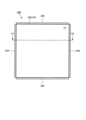
- FIG. 1 is a plan view of a radio wave reflecting device according to an embodiment of the present invention, as viewed from the radio wave incident surface side.
- 2 shows a cross-sectional view of a radio wave reflecting device corresponding to the A1-A2 line shown in FIG. 1 is a plan view of a photovoltaic element used in a radio wave reflecting device according to an embodiment of the present invention
- 3B is a cross-sectional view of the photovoltaic element corresponding to the line B1-B2 shown in FIG. 3A.
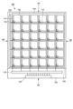
- 1 is a plan view of a radio wave reflecting element constituting a radio wave reflecting device according to an embodiment of the present invention
- 5 shows a cross-sectional view of the radio wave reflecting element corresponding to the C1-C2 line shown in FIG.
- 1 is a plan view of a radio wave reflecting element constituting a radio wave reflecting device according to an embodiment of the present invention
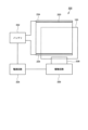
- 1 is a block diagram illustrating a configuration of a radio wave reflecting device according to an embodiment of the present invention
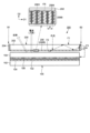
- 1 is a cross-sectional view of a radio wave reflecting device according to an embodiment of the present invention
- 1 is a cross-sectional view of a radio wave reflecting device according to an embodiment of the present invention
- 1 is a cross-sectional view of a radio wave reflecting device according to an embodiment of the present invention
- 1 is a cross-sectional view of a radio wave reflecting device according to an embodiment of the present invention
- 1 is a cross-sectional view of a radio wave reflecting device according to an embodiment of the present invention
- 1 is a cross-sectional view of a radio wave reflecting device according to an embodiment of the present invention
- 1 is a cross-sectional view of a radio wave reflecting device according to an embodiment of the present invention
- 1 is a cross-sectional view of a radio
- This embodiment shows an example of a device that integrally includes a liquid crystal-based radio wave reflector and a solar cell that converts light energy into electrical energy.
- the liquid crystal-based radio wave reflector is a reflector that can reflect radio waves asymmetrically.
- a device that includes a solar cell and a radio wave reflector is referred to as a "radio wave reflecting device.”
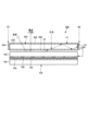
- FIG. 1 shows a plan view of the radio wave reflecting device 300 according to this embodiment when viewed from the radio wave incident surface side.
- FIG. 2 shows a cross-sectional view of the radio wave reflecting device 300 corresponding to the A1-A2 line shown in FIG. 1.
- the radio wave reflecting device 300 includes a radio wave reflecting element 100 and a solar cell 200 arranged on top of the radio wave reflecting element 100.
- the radio wave reflecting element 100 includes a first substrate 150 on which a bias electrode 102 is provided, a second substrate 152 on which a common electrode 104 is provided, and a liquid crystal layer 106 between the first substrate 150 and the second substrate 152.
- the radio wave reflecting element 100 is an element that reflects radio waves transmitted from a base station or the like in a controlled direction, and in the illustrated example, the side of the first substrate 150 is the incident surface of the radio waves.
- the radio wave reflecting device 300 has a structure in which the solar cell 200 is disposed on the first substrate 150, and thus the radio waves pass through the solar cell 200 and enter the radio wave reflecting element 100.
- the radio wave reflecting element 100 and the solar cell 200 are shown separated with an air layer between them.
- the structure shown in FIG. 2 is a schematic example, and the radio wave reflecting element 100 and the solar cell 200 may be provided in contact with each other. Also, a layer of transparent adhesive may be provided between the radio wave reflecting element 100 and the solar cell 200.
- the solar cell 200 includes a light-guiding section 202 and a light-receiving section 204 arranged around the light-guiding section 202.
- the solar cell 200 is arranged so that the light-guiding section 202 overlaps with the radio wave reflecting element 100, and the light-receiving section 204 does not overlap with the radio wave reflecting element 100. More specifically, the light-receiving section 204 is arranged so as not to overlap with the bias electrode 102 and the common electrode 104 of the radio wave reflecting element 100.
- the light-guiding section 202 is a plate-shaped member and has a first surface F1, a second surface F2 opposite the first surface F1, and a side surface F3 between the first surface F1 and the second surface F2.
- the light-receiving section 204 has a light-receiving surface and is arranged so that the light-receiving surface faces the side surface F3.
- the light receiving unit 204 may be disposed so as to be in contact with the side surface F3 of the light guide unit 202, or an optical system (e.g., a lens) that focuses light may be provided between the side surface F3 and the light receiving unit 204.
- the light guide section 202 is an optical member that guides the light incident from the first surface F1 to the side surface F3.
- the light guide section 202 has a characteristic of guiding a part of the light incident from the first surface F1 to the side surface F3 while totally reflecting it internally, and emitting it from the side surface F3.
- the light guide section 202 is a transparent member and is formed of an insulating material that has a low absorption coefficient for at least light in the visible band and the near-infrared band.
- the light guide section 202 is preferably formed of a material that is transparent, can guide light, and has almost no absorption or reflection effects on radio waves in the high-frequency band used in wireless communication.
- the light guide section 202 is preferably formed of a dielectric material such as glass, quartz, or resin.
- the light guide section 202 may be, for example, a flat member called a light guide plate.
- fine particles having a different refractive index from the base material forming the light guide section 202 may be dispersed in the light guide section 202. This configuration allows light to be guided to end F3 while being scattered within the light-guiding section 202.
- the light receiving section 204 is formed of a photovoltaic element that exhibits a photovoltaic effect (hereinafter, the photovoltaic element will be described using the same reference numerals as the light receiving section).
- the photovoltaic element 204 for example, a photovoltaic element using a silicon semiconductor (silicon solar cell), a photovoltaic element using a compound semiconductor such as gallium arsenide, copper, indium, or selenium (compound semiconductor solar cell), or a photovoltaic element using an organic semiconductor (organic solar cell) can be used.
- FIG. 3A shows a plan view of a silicon solar cell as an example of a photovoltaic element 204.
- FIG. 3B shows a cross-sectional view of the silicon solar cell corresponding to the line B1-B2 shown in FIG. 3A.
- FIG. 3A is a schematic diagram of the light receiving surface of a silicon solar cell 200, which has a structure in which a grid-shaped surface electrode 2042 is provided on a photoelectric conversion layer 2044. As shown in FIG. 3B, a back electrode 2046 is provided on the back side of the photoelectric conversion layer 2044. Furthermore, it is preferable that an anti-reflection film 2048 is provided on the light incident surface of the photovoltaic element 204.
- the photoelectric conversion layer 2044 includes a pn junction or a pin junction formed from a silicon semiconductor.
- the surface electrode 2042 is a negative side (n-type semiconductor layer side) electrode
- the back electrode 2046 is a positive side (p-type semiconductor layer side) electrode.
- the surface electrode 2042 and the back electrode 2046 are formed from a metal material such as aluminum.
- the photovoltaic element 204 is arranged along the side of the light-guiding section 202, and thus has a rectangular shape that is elongated in one direction.
- the surface electrode 2042 provided on the light-receiving surface has a grid-like shape to allow light to be incident on the photoelectric conversion layer 2044 and reduce in-plane resistance loss.
- the back electrode 2046 has a solid shape on the entire surface to reflect light that has not been photoelectrically converted back to the photoelectric conversion layer 2044.
- the photovoltaic element 204 has a metal electrode, which can hinder the passage of radio waves, but as shown in FIG. 1 and FIG. 2, the photovoltaic element 204 is arranged outside the radio wave reflecting element 100, and thus is arranged so as not to affect the characteristics of the radio wave reflecting device 300.
- the radio wave reflection device 300 is not limited to this example.
- the light receiving section 204 (photovoltaic element) may be divided into multiple parts on each side of the light guiding section 202.
- the light receiving section 204 does not need to surround the entire circumference of the light guiding section 202, and may be provided on at least a part of the side surface F3 of the light guiding section 202.
- the side surface F3 of the light guiding section 202 on which the light receiving section 204 is not provided may be covered with a metal film and have a structure that reflects the guided light. With such a configuration, it is possible to reduce the light leaking from the light guiding section 202 and increase the amount of light incident on the light receiving section 204.
- the surface on which the solar cell 200 is provided faces outward and is used as a reflecting surface. Therefore, radio waves transmitted from a base station or the like are incident on the radio wave reflecting element 100, and external light is incident on the light guiding section 202 of the solar cell 200.
- external light is incident on the first surface F1 of the light guiding section 202
- a part of the incident light is guided while repeating total reflection in the light guiding section 202 and is emitted from the side surface F3.
- the light emitted from the side surface F3 of the light guiding section 202 is received by the light receiving section (photovoltaic element) 204 and generates electric power.
- the electric power generated by the light receiving section (photovoltaic element) 204 is used as electric power to drive the radio wave reflecting element 100.
- the light guiding section 202 is formed of a material that does not absorb or reflect radio waves, the radio waves incident on the light guiding section 202 are incident on the radio wave reflecting element 100 without attenuation. The radio waves reflected by the radio wave reflecting element 100 then pass through the light guiding section 202 again and are emitted at a specified angle.
- the radio wave reflecting device 300 has a common incident surface for external light and radio waves.
- a light guiding section 202 is provided on the incident surface for external light and radio waves, and because the light guiding section 202 is made of a dielectric, the external light can be guided to the light receiving section (photovoltaic element) 204 and used for power generation, and the radio waves can be directly incident on the radio wave reflecting element 100 and reflected at a predetermined angle.
- FIG. 4 shows a plan view of the radio wave reflecting element 100 constituting the radio wave reflecting device 300.
- FIG. 5 shows a cross-sectional view of the radio wave reflecting element 100 corresponding to the area between C1 and C2 shown in FIG. 4.
- FIG. 4 and FIG. 5 will be made to FIG. 4 and FIG. 5 as appropriate.
- the radio wave reflecting element 100 includes a bias electrode 102, a common electrode 104, and a liquid crystal layer 106 between the bias electrode 102 and the common electrode 104.
- the bias electrodes 102 are arranged in a matrix in the X-axis direction and the Y-axis direction.
- the bias electrodes 102 and the common electrode 104 are arranged so as to overlap in a planar view.
- the common electrode 104 is large enough to overlap with all of the bias electrodes 102 arranged in a matrix. Note that the X-axis direction and the Y-axis direction shown in FIG. 4 are used for explanation, and the X-axis direction and the Y-axis direction can also be interpreted as a first direction and a second direction intersecting the first direction.
- the bias electrode 102 is provided on the first substrate 150, and the common electrode 104 is provided on the second substrate 152.
- the liquid crystal layer 106 is disposed in an area where the surface of the first substrate 150 on which the bias electrode 102 is provided and the surface of the second substrate 152 on which the common electrode 104 is provided face each other with a gap.
- the first substrate 150 has an area that extends outward from the second substrate 152.
- a first drive circuit 118 and a terminal section 122 are provided in this area.
- the first drive circuit 118 has a function of outputting a bias signal to the bias electrode 102.
- the terminal section 122 is an area that forms a connection with an external circuit, and is connected to, for example, a flexible printed circuit board (not shown). A signal and power that control the first drive circuit 118 are input to the terminal section 122.
- the liquid crystal layer 106 contains long, rod-shaped liquid crystal molecules. Since the liquid crystal molecules of the liquid crystal used in this embodiment have dielectric anisotropy, the dielectric constant of the liquid crystal layer 106 changes as the orientation state of the liquid crystal molecules changes. Specifically, the orientation state of the liquid crystal molecules can be changed by the potential difference between the bias electrode 102 and the common electrode 104.
- the bias electrode 102 can be considered to correspond to the patch, the liquid crystal layer 106 to the dielectric, and the common electrode 104 to the ground plate. Since the liquid crystal layer 106 has a variable dielectric constant, the phase of the radio waves reflected by the radio wave reflecting element 100 changes depending on the dielectric constant of the liquid crystal layer 106.
- the radio wave reflecting element 100 can control the orientation state of the liquid crystal molecules in the liquid crystal layer 106 by individually controlling the potential of the bias electrodes 102 arranged in a matrix. In other words, the radio wave reflecting element 100 can partially vary the dielectric constant of the liquid crystal layer 106 within the plane. With this function, the radio wave reflecting element 100 can create a phase difference in the reflected radio waves and control the traveling direction (reflection direction) to the intended direction.
- the initial alignment state of the liquid crystal molecules in the liquid crystal layer 106 is determined by the alignment film.
- a first alignment film 108A is provided on the first substrate 150, and a second alignment film 108B is provided on the second substrate 152.
- the first alignment film 108A is provided so as to cover the bias electrode 102, and the second alignment film 108B is provided so as to cover the common electrode 104.
- the first alignment film 108A and the second alignment film 108B only need to have the function of orienting the liquid crystal molecules, and there are no limitations on the material and manufacturing method.
- the first alignment film 108A and the second alignment film 108B are appropriately selected from vertical alignment films, horizontal alignment films, etc. depending on the type of liquid crystal.
- the first alignment film 108A and the second alignment film 108B are formed of, for example, polyimide.
- the radio wave reflecting element 100 shown in FIG. 4 has a structure in which bias electrodes 102 arranged in a matrix are connected in series for each arrangement in the Y-axis direction by strip wiring 110. Therefore, the radio wave reflecting element 100 shown in FIG. 4 is capable of controlling the potential of the bias electrodes 102 for each arrangement (each column) in the Y-axis direction. On the other hand, a constant voltage is applied to the common electrode 104 in common to the bias electrodes 102 arranged in a matrix. The common electrode 104 is controlled to have, for example, a ground potential. With this configuration, the radio wave reflecting element 100 can reflect incident radio waves at different angles in the left and right directions of the drawing, centered on a reflection axis VR parallel to the Y-axis direction.
- FIG. 6 shows another example of the radio wave reflecting element 100.
- the radio wave reflecting element 100 shown in FIG. 6 has a scanning signal line 112 extending in the X-axis direction and a bias signal line 114 extending in the Y-axis direction.
- the scanning signal line 112 and the bias signal line 114 are provided on a first substrate 150.
- a second drive circuit 120 is provided on the first substrate 150.
- the first drive circuit 118 has a function of outputting a bias signal that controls the alignment state of the liquid crystal
- the second drive circuit 120 has a function of outputting a scanning signal.
- the scanning signal line 112 and the bias signal line 114 are arranged to cross each other with an insulating layer (not shown) sandwiched therebetween.
- the bias signal line 114 is connected to a first drive circuit 118, and the scanning signal line 112 is connected to a second drive circuit 120.
- the bias electrodes 102 arranged in a matrix are each connected to a switching element 116.
- the switching (on and off) of the switching elements 116 is controlled by a scanning signal of the scanning signal line 112.
- the bias electrodes 102 arranged in a matrix are selected for each arrangement in the X-axis direction, and a bias signal is applied from the bias signal line 114.
- the switching elements 116 are formed, for example, of thin film transistors.
- the configuration of the radio wave reflecting element 100 shown in FIG. 6 makes it possible to apply a bias signal individually to each of the bias electrodes 102 arranged in a matrix. Therefore, the radio wave reflecting element 100 shown in FIG. 6 can control the direction of propagation of the reflected wave of the incident radio wave in the left-right direction of the drawing, centered on a reflection axis VR parallel to the Y-axis direction, and can also control the direction of propagation of the reflected wave in the up-down direction of the drawing, centered on a reflection axis HR parallel to the X-axis direction.
- FIG. 7 shows a block diagram of the radio wave reflecting device 300.
- the radio wave reflecting device 300 includes a battery 302 that stores electricity generated by the light receiving unit 204, a drive circuit 306 that drives the radio wave reflecting element 100, a power supply circuit 304 that supplies power from the battery 302 to the drive circuit 306, and a flexible wiring board 308 that connects the drive circuit 306 and the radio wave reflecting element 100.
- the radio wave reflecting device 300 may be configured such that the battery 302 is omitted and the output of the photovoltaic element 204 is directly supplied to the power supply circuit 304. However, by providing the radio wave reflecting device 300 with the battery 302, it is possible to store surplus power and drive the radio wave reflecting element 100 even at night.
- the radio wave reflecting device 300 includes a solar cell 200, and can supply power for driving the radio wave reflecting element 100.
- the solar cell 200 is composed of a light guide plate 202 and a light receiving section 204 arranged on the periphery of the light guide section 202.
- the radio wave reflecting plate 300 is arranged so that the light guide section 202, which does not affect radio waves, covers the front surface of the radio wave reflecting element 100, and the light receiving section 204 is arranged outside the radio wave reflecting element 100.
- This arrangement ensures a light receiving area for the solar cell 200, and prevents the radio wave reflecting element 100 from being affected by the reflection of radio waves.
- a film-type battery can be used as the battery 302.
- the film-type battery can be installed on the back surface of the radio wave reflecting element 100. With this configuration, the radio wave reflecting device 300 can be installed and driven even in places where it is difficult to secure a power source.
- the radio wave reflecting device 300 of this embodiment has the solar cell 200 disposed on the reflecting surface of the radio wave reflecting element 100, and the light receiving surface of the solar cell 200 is made of a material that does not affect the transmission of radio waves, so that it can generate power using external light while driving the radio wave reflecting element 100 to reflect incident radio waves in a predetermined direction.
- the radio wave reflecting device 300 can use the power generated by the solar cell 200 as power to drive the radio wave reflecting element 100, so the radio wave reflecting device 300 can be installed even in places where it is difficult to secure a power source.
- This embodiment shows an example of a radio wave reflecting device 300 having a different configuration from that of the first embodiment in terms of the light guiding section 202.
- the differences from the first embodiment will be mainly described, and descriptions of overlapping parts will be omitted as appropriate.
- FIG. 8 shows a cross-sectional view of a radio wave reflecting device 300 according to this embodiment.
- the radio wave reflecting device 300 has a structure in which a solar cell 200 is arranged on top of the front surface of a radio wave reflecting element 100.
- the solar cell 200 includes a light guiding section 202 and a light receiving section 204, and a functional member 206 for guiding external light is added to the light guiding section 202.
- the functional member 206 is disposed on the second surface F2 side of the light guide section 202.
- the functional member 206 is, for example, a reflective diffraction grating 206A.
- the reflective diffraction grating 206A has a structure in which grooves (parallel grooves) are formed on a flat plate surface formed by a dielectric substrate 2061, and a metal thin film 2062 is provided on the surface.
- the reflective diffraction grating 206A is preferably provided so as to overlap the entire surface on the second surface F2 side of the light guide section 202.
- the reflective diffraction grating 206A has a metal thin film 2062 formed on the surface to reflect incident light at a predetermined diffraction angle, but it is preferable that the metal thin film 2062 is thin in order to reduce the influence on radio waves.
- the metal thin film 2062 formed on the surface of the reflective diffraction grating 206A is preferably, for example, 50 nm or less. Such a thin metal thin film 2062 can reflect radio waves without attenuating them, although there is a slight decrease in reflectivity.
- FIG. 8 shows a configuration in which the functional member 206 is disposed on the second surface F2 side of the light-guiding section 202, the functional member 206 may also be disposed on the first surface F1 side of the light-guiding section 202.
- the radio wave reflecting device 300 has a configuration in which, in addition to the configuration shown in the first embodiment, a functional member 206 is added to the light-guiding section 202 that constitutes the solar cell 200.
- the configuration according to the second embodiment can increase the amount of light guided through the light-guiding section 202, and can increase the amount of power generated by the photovoltaic element 204.
- the other configurations are the same as those of the first embodiment, and the same effects can be obtained.
- This embodiment shows an example of a radio wave reflecting device 300 in which the configuration of the functional member 206 is different from that of the second embodiment.
- the differences from the second embodiment will be mainly described, and descriptions of overlapping parts will be omitted as appropriate.
- FIG. 9 shows the configuration of a radio wave reflecting device 300 according to this embodiment.
- FIG. 9 shows a configuration in which an optical diffraction layer 206B is used as the functional member 206.
- the optical diffraction layer 206B has the property of reflecting and diffracting at least a portion of the incident light in a wavelength band toward the light guide section 202.
- the optical diffraction layer 206B has optical anisotropy (birefringence) and has multiple optical axes.
- the optical anisotropy is, for example, uniaxial optical anisotropy.
- FIG. 9 shows a schematic structure of the light diffraction layer 206B in the inset.
- the light diffraction layer 206B includes a plurality of spiral structures 2063.
- Each of the spiral structures 2063 extends in the D2 direction and is arranged at intervals P in the D1 direction.
- the D2 direction in which each of the spiral structures 2063 extends is approximately perpendicular to the second surface F2 of the light guide section 202.
- the multiple spiral structures 2063 are composed of, for example, multiple liquid crystal molecules 2064.
- the multiple spiral structures 2063 have a structure in which multiple liquid crystal molecules 2064 are stacked while spirally rotating along the D2 direction.
- each of the spiral structures 2063 has a structure in which multiple liquid crystal molecules 2064 are arranged in a spiral shape while changing their orientation direction along the D2 direction. Since the spiral period of the spiral structures 2063 is relatively large, the optical diffraction layer 206B functions as a reflective diffraction grating that reflects light.
- the optical diffraction layer 206B has a number of helical structures 2063 in which a number of liquid crystal molecules are stacked while changing their orientation in a helical manner along the D2 direction, and such a number of helical structures 2063 are periodically arranged in the D1 direction, so that the optical diffraction layer 206B has a structure in which the refractive index changes gradually, and Fresnel reflection gradually occurs for incident light.
- the Fresnel reflection is strongest at the position where the refractive index changes the most.
- the reflective surface FR is shown by connecting the areas where the Fresnel reflection is strongest with straight lines.
- the light diffraction layer 206B forms a plurality of reflective surfaces FR.
- the reflective surfaces FR are approximately parallel to each other.
- the reflective surfaces FR are inclined with respect to the second surface F2 of the light guide section 202 and have a substantially planar shape extending in a fixed direction.
- the reflective surfaces FR selectively reflect the light incident from the light guide section 202 in accordance with Bragg's law.
- the light diffraction layer 206B reflects and diffracts light of at least a portion of the wavelength band of the incident light, and causes it to re-enter the light guide section 202.
- the optical diffraction layer 206B preferably transmits at least a portion of the light in the visible light band among the light incident on the optical diffraction layer 206B from the light guiding section 202, and reflects and diffracts a portion of the light from the visible light band to the near-infrared light band.
- the optical diffraction layer 206B reflects and diffracts at least a portion of the incident light, so that the diffracted light can be made to enter the light guiding section 202 again and guided. This can increase the amount of light guided by the light guiding section 202 and emitted from the side surface F3.
- the light guided by the light guiding section 202 and emitted from the side surface F3 can be light of a specific wavelength band.
- the light of the specific wavelength band is preferably light of a wavelength band with high light collection efficiency in the photovoltaic element 204.
- the light diffraction layer 206B may be in contact with the light guide section 202, or a transparent layer such as an adhesive layer may be interposed between the light diffraction layer 206B and the light guide section 202.
- the light diffraction layer 206B may be flexible, for example. It is preferable that the refractive index of the layer interposed between the light diffraction layer 206B and the light guide section 202 is approximately equal to the refractive index of the light guide section 202.
- the light diffraction layer 206B forms a reflective diffraction grating using a liquid crystal layer.
- Cholesteric liquid crystal can be used as the liquid crystal material.
- the light diffraction layer 206B is formed from a pair of glass substrates, a light distribution film, and a liquid crystal material, and does not use electrodes. Therefore, it can transmit radio waves without absorbing them.
- the functional member 206 shown in the second embodiment is formed from an optical diffraction layer 206B using a liquid crystal material, thereby making it possible to increase the amount of light guided through the light guide section 202 and increase the amount of power generated by the photovoltaic element 204.
- the other configurations are the same as those of the first embodiment, and the same effects can be obtained.
- a wavelength-converting member may be further added to the configuration of the light-guiding section 202 shown in the second and third embodiments.
- FIG. 10 shows the configuration of a radio wave reflecting device 300 according to this embodiment.
- a wavelength conversion layer 208 is provided on the first surface F1 side of the light-guiding section 202.
- the functional member 206 (light diffraction layer 206B) shown in the third embodiment has improved wavelength selectivity for diffracted light. Therefore, by using the wavelength conversion layer 208 to convert the wavelength to match the wavelength of the functional member 206 (light diffraction layer 206B), the utilization efficiency of the incident light can be improved.
- the wavelength conversion layer 208 converts all or part of the light from the ultraviolet band to the visible light band into light in the near-infrared band, thereby improving the efficiency of light utilization.
- the wavelength conversion layer 208 converts the visible light that is the incident light into light in a wavelength band that is highly collected by the photovoltaic element 204 (e.g., infrared light), but it may also be a layer that converts ultraviolet light into visible light or infrared light, or a layer that converts infrared light into visible light.
- a wavelength conversion layer 208 can be formed, for example, by applying an inorganic phosphor or an organic fluorescent material.
- the light guide section 202 by providing a wavelength conversion layer 208 in the light guide section 202, it is possible to increase the amount of light in a specific wavelength band among the light diffracted by the functional member 206 (light diffraction layer 206B) and re-entered into the light guide section 202, thereby increasing the amount of power generated by the photovoltaic element 204.
- the other configurations are the same as in the first embodiment, and the same effects can be obtained.
- a light scattering body may be used instead of the diffraction grating.
- FIG. 11 shows a cross-sectional view of the radio wave reflecting device 300 according to this embodiment.
- a light scattering layer 206C that scatters light transmitted through the light guide section 202 is used as the functional member 206.
- the light scattering layer 206C has a structure in which fine particles 2066 that scatter light are dispersed in a resin layer 2065 molded into a sheet shape. It is preferable that the fine particles 2066 have a particle size approximately equal to the wavelength of the light to be scattered. The particle size of the fine particles 2066 is not uniform, and fine particles of different particle sizes may be mixed together to scatter light in a specified wavelength band.
- the resin layer 2065 is formed of, for example, an acrylic, epoxy, vinyl, fluorine, or polyester resin.
- the fine particles 2066 are formed of an inorganic material or an organic material (resin material).
- the fine particles 2066 may be formed of a material such as titanium oxide or silica.
- FIG. 11 shows an example in which the resin layer 2065 has a flat surface, but the surface of the resin layer 2065 may be uneven due to the fine particles 2066.
- the functional member 206 shown in this embodiment can scatter light that has passed through the light-guiding section 202 and cause the scattered light to reenter the light-guiding section 202, thereby increasing the amount of light incident on the photovoltaic element 204.
- the resin layer 2065 since the resin layer 2065 only has fine particles 2066 dispersed therein, it is possible to prevent attenuation of radio waves that are incident on and reflected by the radio wave reflecting element 100.
- the other configurations are the same as those in the first embodiment, and the same effects can be obtained.
- This embodiment shows a radio wave reflecting device 300 having a structure in which the configuration of the light guiding section 202 is different from that of the first embodiment.
- the differences from the first embodiment will be mainly described, and common parts will be omitted as appropriate.
- FIG. 12 shows a cross-sectional view of the radio wave reflecting device 300 according to this embodiment.
- the radio wave reflecting device 300 has a structure in which a solar cell 200 and a radio wave reflecting element 100 are arranged one on top of the other.
- the solar cell 200 includes a light guide section 202 and a light receiving section 204, and the light guide section 202 is formed, for example, by a light guide plate 202.
- the light guide plate 202 has an uneven structure on its surface. The uneven structure may be provided on only one of the first surface F1 side and the second surface F2 side of the light guide plate 202, or may be provided on both surfaces.
- the uneven structure may have a periodic uneven structure, or may be a random unevenness (frosted glass-like) in which the unevenness does not have periodicity.
- the light guide plate 202 is formed of a resin material such as acrylic, or an inorganic material such as glass.
- Fine particles with different refractive indices such as titanium oxide, may also be dispersed in the light guide plate 202.
- the configuration of the light guide section 202 shown in this embodiment makes it possible to suppress surface reflection of external light, guide the incident light, and increase the amount of light incident on the photovoltaic element 204.
- the light guide plate 202 is made of a dielectric material, and the uneven structure formed on the surface does not affect radio waves, so attenuation of radio waves incident on and reflected from the radio wave reflecting element 100 can be prevented.
- the other configurations are the same as those of the first embodiment, and the same effects can be obtained.
- the configuration of the light guide section 202 shown in this embodiment can be replaced with the light guide section 202 in the second to fifth embodiments.
- the radio wave reflecting device 300 has a configuration in which a solar cell 200 is superimposed on a radio wave reflecting element 100 (more specifically, a configuration in which a light guiding section 202 is superimposed on the radio wave reflecting element 100), but in order to improve the gain of the reflected radio waves, it is preferable that the light guiding section 202 and the first substrate 150 of the radio wave reflecting element 100 have a predetermined thickness.
- FIG. 13A shows a cross-sectional view of the radio wave reflecting device 300.
- FIG. 13A shows that the radio wave reflecting element 100 and the light guiding section 202 constituting the solar cell 200 are arranged in close contact with each other, and that the total thickness of the first substrate 150 and the light guiding section 202 is Ta.
- a transparent adhesive may be interposed between the first substrate 150 and the light guiding section 202. It is preferable that the refractive index of the transparent adhesive is approximately the same as that of the first substrate 150 or the light guiding section 202.
- thickness Ta which is the total thickness of light-guiding section 202 and first substrate 150, has a thickness equivalent to ⁇ /4 (a quarter wavelength) when the wavelength of the radio wave is ⁇ .
- ⁇ /4 a quarter wavelength
- the total thickness Ta of the first substrate 150 and the light guiding section 202 is equivalent to 1/4 of the wavelength of the radio wave, so that attenuation of the reflected wave can be prevented.
- the light guiding section 202 can be selected to satisfy the relationship of formula (1) according to the frequency of the target radio wave, so that the configuration of this embodiment increases the degree of freedom in the design of the radio wave reflecting device 300.
- an air layer 210 may be interposed between the first substrate 150 and the light-guiding section 202.
- the thickness Tb of the air layer 210 is equal to or less than one-tenth of the wavelength of the incident radio wave (Tb ⁇ /10)
- the thickness Te of the first substrate 150 and the thickness Td of the light-guiding section 202 are each equivalent to 1/4 of the wavelength of the radio waves.
- the configuration of the radio wave reflecting device 300 according to this embodiment makes it possible to prevent attenuation of radio waves reflected by the radio wave reflecting element 100 and improve the gain of the reflected waves.
- the other configurations are the same as those of the first embodiment, and the same effects can be obtained.
- the configuration of the light guide section 202 shown in this embodiment can be replaced with the light guide section 202 in the second to sixth embodiments.
- the configurations of the radio wave reflecting device shown in the first to seventh embodiments can be combined as appropriate as long as they are not mutually contradictory. Furthermore, based on each embodiment, those in which a person skilled in the art appropriately adds or removes components or modifies the design, or adds or omits processes or modifies conditions, are also included in the scope of the present invention as long as they include the gist of the present invention.
Landscapes
- Photovoltaic Devices (AREA)
Priority Applications (2)
| Application Number | Priority Date | Filing Date | Title |
|---|---|---|---|
| JP2025532731A JPWO2025013756A1 (https=) | 2023-07-13 | 2024-07-04 | |
| CN202480039203.3A CN121312020A (zh) | 2023-07-13 | 2024-07-04 | 电波反射装置 |
Applications Claiming Priority (2)
| Application Number | Priority Date | Filing Date | Title |
|---|---|---|---|
| JP2023115084 | 2023-07-13 | ||
| JP2023-115084 | 2023-07-13 |
Related Child Applications (1)
| Application Number | Title | Priority Date | Filing Date |
|---|---|---|---|
| US19/435,811 Continuation US20260128529A1 (en) | 2023-07-13 | 2025-12-30 | Radio wave reflecting device |
Publications (1)
| Publication Number | Publication Date |
|---|---|
| WO2025013756A1 true WO2025013756A1 (ja) | 2025-01-16 |
Family
ID=94215483
Family Applications (1)
| Application Number | Title | Priority Date | Filing Date |
|---|---|---|---|
| PCT/JP2024/024278 Pending WO2025013756A1 (ja) | 2023-07-13 | 2024-07-04 | 電波反射装置 |
Country Status (3)
| Country | Link |
|---|---|
| JP (1) | JPWO2025013756A1 (https=) |
| CN (1) | CN121312020A (https=) |
| WO (1) | WO2025013756A1 (https=) |
Citations (5)
| Publication number | Priority date | Publication date | Assignee | Title |
|---|---|---|---|---|
| JPS60203599A (ja) * | 1984-03-29 | 1985-10-15 | 日本電気株式会社 | 太陽光発電衛星 |
| JP2019519136A (ja) * | 2016-05-03 | 2019-07-04 | カイメタ コーポレイション | 光起電力セルと一体化したアンテナ |
| CN113764900A (zh) * | 2021-08-23 | 2021-12-07 | 西安电子科技大学 | 一种集成有太阳能电池的混合可重构智能反射表面 |
| WO2022085248A1 (ja) * | 2020-10-22 | 2022-04-28 | 株式会社ジャパンディスプレイ | 太陽電池装置 |
| WO2023058399A1 (ja) * | 2021-10-07 | 2023-04-13 | 株式会社ジャパンディスプレイ | 電波反射装置 |
-
2024
- 2024-07-04 JP JP2025532731A patent/JPWO2025013756A1/ja active Pending
- 2024-07-04 WO PCT/JP2024/024278 patent/WO2025013756A1/ja active Pending
- 2024-07-04 CN CN202480039203.3A patent/CN121312020A/zh active Pending
Patent Citations (5)
| Publication number | Priority date | Publication date | Assignee | Title |
|---|---|---|---|---|
| JPS60203599A (ja) * | 1984-03-29 | 1985-10-15 | 日本電気株式会社 | 太陽光発電衛星 |
| JP2019519136A (ja) * | 2016-05-03 | 2019-07-04 | カイメタ コーポレイション | 光起電力セルと一体化したアンテナ |
| WO2022085248A1 (ja) * | 2020-10-22 | 2022-04-28 | 株式会社ジャパンディスプレイ | 太陽電池装置 |
| CN113764900A (zh) * | 2021-08-23 | 2021-12-07 | 西安电子科技大学 | 一种集成有太阳能电池的混合可重构智能反射表面 |
| WO2023058399A1 (ja) * | 2021-10-07 | 2023-04-13 | 株式会社ジャパンディスプレイ | 電波反射装置 |
Also Published As
| Publication number | Publication date |
|---|---|
| JPWO2025013756A1 (https=) | 2025-01-16 |
| CN121312020A (zh) | 2026-01-09 |
Similar Documents
| Publication | Publication Date | Title |
|---|---|---|
| US6473220B1 (en) | Film having transmissive and reflective properties | |
| US9157605B2 (en) | Illumination device | |
| US20190288145A1 (en) | Light-Concentrating Mechanism, Photovoltaic Power Generation Device, Window Structure, and Glass Window | |
| US20020180909A1 (en) | Device having reflective and transmissive properties | |
| US20090266413A1 (en) | Photovoltaic Cells With Gratings For Scattering Light Into Light-absorption Layers | |
| JP2006243485A (ja) | 透過光自動調光セル及び部材 | |
| CN113764900A (zh) | 一种集成有太阳能电池的混合可重构智能反射表面 | |
| US7847183B2 (en) | Three dimensional photo voltaic modules in an energy reception panel | |
| US20160048043A1 (en) | Optical Diode Comprising Components Made From Metamaterials | |
| JP2011135011A (ja) | 光起電力素子モジュールおよびその製造方法 | |
| JP5590965B2 (ja) | 光起電力素子モジュールおよびその製造方法 | |
| JP7667818B2 (ja) | ガラス建材 | |
| CN102305959B (zh) | 具有光栅结构的聚光系统 | |
| US8884156B2 (en) | Solar energy harvesting device using stimuli-responsive material | |
| CA2399065C (en) | Multiflecting light directing film | |
| WO2025013756A1 (ja) | 電波反射装置 | |
| JP6763614B2 (ja) | 光導波装置、光電変換装置、建築物、電子機器および発光装置 | |
| KR101025929B1 (ko) | 광도파로를 구비하는 태양전지 모듈 | |
| US20260128529A1 (en) | Radio wave reflecting device | |
| JP4924724B2 (ja) | 太陽電池パネル | |
| US20240021747A1 (en) | Photovoltaic cell device | |
| CN217656592U (zh) | 太阳能电池模组 | |
| Yu et al. | High-gain lens antenna using transmissive phase gradient metasurface | |
| US12446392B2 (en) | Photovoltaic cell device | |
| US20230246590A1 (en) | Solar power generation apparatus |
Legal Events
| Date | Code | Title | Description |
|---|---|---|---|
| 121 | Ep: the epo has been informed by wipo that ep was designated in this application |
Ref document number: 24839648 Country of ref document: EP Kind code of ref document: A1 |
|
| ENP | Entry into the national phase |
Ref document number: 2025532731 Country of ref document: JP Kind code of ref document: A |
|
| NENP | Non-entry into the national phase |
Ref country code: DE |