WO2025013178A1 - 光変調器および光変調器パッケージ - Google Patents
光変調器および光変調器パッケージ Download PDFInfo
- Publication number
- WO2025013178A1 WO2025013178A1 PCT/JP2023/025473 JP2023025473W WO2025013178A1 WO 2025013178 A1 WO2025013178 A1 WO 2025013178A1 JP 2023025473 W JP2023025473 W JP 2023025473W WO 2025013178 A1 WO2025013178 A1 WO 2025013178A1
- Authority
- WO
- WIPO (PCT)
- Prior art keywords
- pair
- optical
- optical modulator
- resistors
- electrical
- Prior art date
- Legal status (The legal status is an assumption and is not a legal conclusion. Google has not performed a legal analysis and makes no representation as to the accuracy of the status listed.)
- Ceased
Links
Images




Classifications
-
- G—PHYSICS
- G02—OPTICS
- G02F—OPTICAL DEVICES OR ARRANGEMENTS FOR THE CONTROL OF LIGHT BY MODIFICATION OF THE OPTICAL PROPERTIES OF THE MEDIA OF THE ELEMENTS INVOLVED THEREIN; NON-LINEAR OPTICS; FREQUENCY-CHANGING OF LIGHT; OPTICAL LOGIC ELEMENTS; OPTICAL ANALOGUE/DIGITAL CONVERTERS
- G02F1/00—Devices or arrangements for the control of the intensity, colour, phase, polarisation or direction of light arriving from an independent light source, e.g. switching, gating or modulating; Non-linear optics
- G02F1/01—Devices or arrangements for the control of the intensity, colour, phase, polarisation or direction of light arriving from an independent light source, e.g. switching, gating or modulating; Non-linear optics for the control of the intensity, phase, polarisation or colour
Definitions
- This disclosure relates to optical modulators and optical modulator packages.
- Mach-Zehnder optical modulators have low wavelength dependency, are essentially free of wavelength chirp components, and are fast, so they are widely used in optical communications, from medium- and long-distance optical communications using coherent systems to IMDD (direct modulation with direct detection) systems of several hundred meters.
- IMDD direct modulation with direct detection
- a Mach-Zehnder optical modulator is structured so that light incident on the input optical waveguide is split into two optical waveguides (arm optical waveguides) with an intensity ratio of approximately 1:1, and the split light is propagated a certain distance before being recombined and output.
- the phase of the two lights By changing the phase of the two lights using a phase modulation region provided in the two branched optical waveguides, it is possible to change the interference conditions of the light when combined and modulate the intensity or phase of the output light.
- the materials constituting the optical waveguide in the phase modulation region include dielectrics such as LiNbO3 and semiconductors such as InP, GaAs, and Si (silicon).
- the phase of the light propagating through the optical waveguide is changed by inputting a modulating electrical signal to an electrode arranged near the optical waveguide and applying a voltage to the optical waveguide.
- a modulating electrical signal to an electrode arranged near the optical waveguide and applying a voltage to the optical waveguide.
- V ⁇ half-wave voltage
- One non-limiting objective of this disclosure is to enable performance measurement (or characteristic testing) of a single optical modulator having a termination resistor.
- An optical modulator includes a pair of optical waveguides that guide each of the light beams branched from the input light, a pair of electrodes that correspond to the pair of optical waveguides and to which a modulating electrical signal for modulating the input light is input, and a pair of termination resistors that correspond to the pair of electrodes and are not electrically connected to each other.
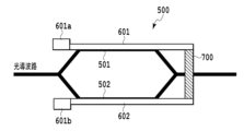
- FIG. 1 is a schematic top view showing a configuration example of a Mach-Zehnder optical modulator (MZM).
- MZM Mach-Zehnder optical modulator
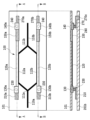
- FIG. 3 is a diagram showing a schematic diagram of an example of an MZM package including the MZM 100 shown in FIG. 2.
- 1A to 1C are diagrams illustrating an example of an MZM package including an MZM according to a first modified example of the first embodiment; 11 is a diagram showing a schematic diagram of an example of an MZM package including an MZM according to a second modification of the first embodiment;
- FIG. 13 is a schematic top view showing a configuration example of an MZM according to a second embodiment.
- FIG. 13 is a diagram illustrating an example of an MZM package including an MZM according to a second embodiment.
- FIG. 13 is a schematic top view showing a configuration example of an MZM according to a third embodiment.
- FIG. 13 is a diagram illustrating an example of an MZM package including an MZM according to a third embodiment.
- V ⁇ One of the performance indices of a Mach-Zehnder optical modulator (MZM) is the half-wave voltage, denoted as V ⁇ .
- the half-wave voltage V ⁇ is the voltage for changing the phase of light by ⁇ , and the smaller the half-wave voltage V ⁇ , the less voltage (or power) required to drive the optical modulator. Since there is an upper limit to the voltage amplitude of the drive circuit that provides the modulated electrical signal to the optical modulator, if the half-wave voltage V ⁇ is larger than the voltage amplitude of the drive circuit, a sufficient amount of phase change or sufficient intensity modulation cannot be obtained, and the quality of the transmission signal may deteriorate.
- the half-wave voltage V ⁇ can vary from wafer lot to wafer lot or chip to chip due to process variations. Therefore, when mass-producing communication modules that include MZMs, it may be necessary to perform a characteristic test of the half-wave voltage V ⁇ in advance.
- Non-Patent Document 1 as shown in FIG. 1, for example, a termination resistor 700 is connected between traveling-wave electrodes 601 and 602 provided for optical waveguides 501 and 502 that form two parallel arms constituting an MZM 500.
- the optical waveguides that form the arms may be conveniently referred to as “arm waveguides,” and the traveling-wave electrodes may be conveniently referred to as “arm electrodes.”
- Mounting pads 601a and 602a are provided at one end of each of the traveling wave electrodes 601 and 602, which are electrically connected to a driving circuit (not shown), and a modulated electrical signal is applied from the driving circuit (not shown) to each of the traveling wave electrodes 601 and 602 via the mounting pads 601a and 602a.
- the termination resistor 700 is connected between the traveling wave electrodes 601 and 602, so a direct current (DC) bias is not applied to only the traveling wave electrode corresponding to one of the two arms. This prevents DC measurements, such as the measurement of the half-wave voltage V ⁇ , and prevents, for example, characteristic testing of individual chips in the wafer state.
- DC direct current
- a structure is described in which the termination resistor is divided for each arm electrode, and the division of the termination resistor is released when the MZM is mounted on a package substrate (or a module substrate).
- An example of a structure in which the division is released is a structure in which resistors provided individually for the arm electrodes are electrically connected (in other words, short-circuited) when the MZM is mounted on a package substrate to form a termination resistor.
- resistors provided individually for the arm electrodes are electrically connected (in other words, short-circuited) when the MZM is mounted on a package substrate to form a termination resistor.
- no termination resistor is formed between the arm electrodes at the stage before the MZM is mounted on a package substrate, making it possible to measure the characteristics of the MZM alone, for example, to measure the half-wave voltage V ⁇ .
- first embodiment for example, in flip chip (FC) mounting, a structure is described in which wiring provided on a package substrate and a mounting pad of an MZM are electrically connected by a bump, and resistors provided for each arm electrode are electrically connected to form a termination resistor.
- FC flip chip
- the MZM 100 is a schematic top view showing an example of the configuration of a Mach-Zehnder optical modulator (MZM) 100 according to the first embodiment.
- the MZM 100 illustratively includes an optical circuit board 101, and, as examples of optical circuits formed on the optical circuit board 101, an input optical waveguide 110a, a branching coupler 111a, optical waveguides 112a and 112b corresponding to the two arm waveguides, a multiplexing coupler 111b, and an output optical waveguide 110b.
- light input to input optical waveguide 110a is branched into two at branching coupler 111a, and the two branched lights propagate through arm waveguides 112a and 112b, respectively, and are input to multiplexing coupler 111b.
- Multiplexing coupler 111b combines the light input from each of arm waveguides 112a and 112b, and outputs the combined light to output optical waveguide 110b.
- MZM 100 illustratively includes traveling-wave electrodes 120a and 120b provided corresponding to arm waveguides 112a and 112b, electrical pads 130a and 130b connected to one end of traveling-wave electrodes 120a and 120b, termination resistors 150a and 150b connected to the other end of traveling-wave electrodes 120a and 120b, and electrical pads 140a and 140b connected to the other end of termination resistors 150a and 150b.
- the "electrical pads” may be referred to as "mounting pads.”
- Mounting pads 130a and 130b are each electrically connected to a drive circuit (not shown), and a modulated electrical signal is provided from the drive circuit to traveling wave electrodes 120a and 120b via mounting pads 130a and 130b.
- the phase of the light that is split into two by the splitting coupler 111a and propagates through each of the arm waveguides 112a and 112b changes, and the optical interference conditions in the multiplexing coupler 111b change.
- the intensity or phase of the light output from the multiplexing coupler 111b to the output optical waveguide 110b is modulated.
- a semiconductor material such as Si, InP, or GaAs, or a dielectric material such as LiNbO3 may be used, for example.
- the termination resistors 150a and 150b are electrically isolated from each other (in other words, insulated) on the optical circuit board 101.
- the mounting pads 140a and 140b are electrically connected to each other via bump connections during FC mounting, for example, so that the other ends of the termination resistors 150a and 150b are electrically connected to each other (in other words, short-circuited).
- termination resistors 150a and 150b form a termination resistor between traveling-wave electrodes 120a and 120b in conjunction with bump connection during FC implementation. Therefore, the resistance value of each of termination resistors 150a and 150b has a resistance value that is, for example, a division of the intended resistance value of the termination resistor connected between traveling-wave electrodes 120a and 120b.
- the termination resistors 150a and 150b that are insulated from each other on the optical circuit board 101 will be referred to as partial termination resistors (or split termination resistors) 150a and 150b, respectively.
- the pair of partial termination resistors 150a and 150b may be referred to as partial termination resistor pair 150 for convenience.
- the termination resistor formed by shorting the partial termination resistors 150a and 150b by bump connection in FC mounting will be referred to as composite termination resistor 150ab for convenience.
- the electrical connection between the mounting pads 140a and 140b can be formed, for example, by bump-connecting each of the mounting pads 140a and 140b to electrical wiring provided on the package substrate 201 (described later in FIG. 3).
- FIG. 3 is a schematic diagram showing an example of an MZM package (or MZM module) including the MZM 100 shown in FIG. 2.
- FIG. 3 shows, as an example, an optical circuit board 101 including the MZM 100 FC-mounted on a package board 201. Because of the FC mounting, the optical circuit board 101 and the package board 201 are bump-connected with their surfaces on which the optical circuit or electrical wiring is provided facing each other, as shown in the lower part of FIG. 3, for example.
- the A-A cross section or B-B cross section shown in the upper part of Figure 3 corresponds to the structure shown in the lower part of Figure 3.
- a set of components is distinguished from each other by adding "a” or "b” to the reference symbol "120", for example, "120a” and "120b", in the upper part of Figure 3, the addition of "a” and "b” is omitted in the lower part of Figure 3, and a set of components is shown without distinction from each other.
- This method of notating symbols is the same in the following explanations and drawings used.
- the pair of mounting pads 130a and 130b may be referred to as mounting pad pair 130, and the pair of mounting pads 140a and 140b may be referred to as mounting pad pair 140.
- the package substrate 201 has, for example, on its upper surface, electrical wiring 210a and 210b to which an electrical modulation signal is provided from the drive circuit, and electrical wiring 220 having a length capable of electrically connecting between the mounting pad pair 140 on the optical circuit board 101.
- Two bumps 230 are provided on the top of each of the electrical wirings 210a and 210b during FC mounting, allowing electrical connection to the mounting pad pair 130 on the optical circuit board 101.
- two bumps 240 are provided on the top of each of both ends of the electrical wiring 220 during FC mounting, which enable electrical connection with the mounting pad pair 140 on the optical circuit board 101.
- the optical circuit board 101 is connected to the package substrate 201 by two bumps 230 and two bumps 240, for example, with the surface on which the MZM 100 is provided facing downward. With this connection, the mounting pad pair 130 of the optical circuit board 101 is electrically connected to the electrical wiring 210a and 210b, respectively, via the bumps 230.
- the mounting pad pair 140 connected to the partial termination resistor pair 150 is connected to the electrical wiring 220 via the bump 240, thereby shorting the partial termination resistor pair 150 and forming a composite termination resistor 150ab.
- the composite termination resistor 150ab is connected between the traveling wave electrodes 120a and 120b.
- the MZM 100 (optical circuit board 101) is FC mounted on the package board 201
- the partial termination resistors 150a and 150b provided individually for the traveling-wave electrodes 120a and 120b are electrically connected, and a composite termination resistor 150ab is formed between the traveling-wave electrodes 120a and 120b.
- the mounting pad pairs 140 of the MZM 100 may be electrically connected by wire bonding to electrically connect the partial termination resistor pairs 150 to form the composite termination resistor 150ab.
- FIG. 4 is a schematic diagram showing an example of an MZM package (or MZM module) including an MZM 100 according to variant 1 of the first embodiment.
- FIG. 4 exemplarily shows an optical circuit board 101 including an MZM 100 FU-mounted on a package board 201a. Because of the FU mounting, the optical circuit board 101 is mounted on the top of the package board 201a with the surface on which the MZM 100 is mounted facing up, as shown in the lower part of FIG. 4.
- the upper part of Figure 4 shows an example of the optical circuit board 101 provided on the top of the package substrate 201a, as viewed from directly above.
- the cross section taken along the line A-A or the line B-B shown in the upper part of Figure 4 corresponds to the structure shown in the lower part of Figure 4.
- the reference symbols 250a, 250b, and 260 indicate electric wires, which are conveniently and diagrammatically represented by curved lines so that it is easy to visually and intuitively grasp that they are electric wires. Therefore, the top view and the cross-sectional view taken along the line A-A in FIG. 4 may be inaccurate when focusing on the electric wires, but are merely for the convenience of explanation.
- the package substrate 201a does not need to be provided with electrical wiring 210a, 210b, and 220 that is electrically connected to the mounting pad pair 130 and the mounting pad pair 140, respectively, as illustrated in FIG. 3.
- the mounting pad pairs 130 are electrically connected, for example to the driver circuitry, by bonding of individual electrical wires 250a and 250b. Additionally, the mounting pad pairs 140 to which the partial termination resistor pairs 150 are connected are electrically connected by bonding of electrical wires 260.
- the mounting pad pair 140 is electrically connected by the electrical wire 260, and the partial termination resistor pair 150 is electrically connected to form the composite termination resistor 150ab. This connects the composite termination resistor 150ab between the traveling wave electrodes 120a and 120b.
- the partial termination resistors 150a and 150b are electrically isolated (or insulated) from each other, so it is permissible to apply a DC bias to one of the traveling wave electrodes 120a and 120b of the MZM100. Therefore, as in the first embodiment described above, it is possible to measure the characteristics of the MZM100 alone.
- FIG. 5 is a diagram showing a schematic example of an MZM package (or an MZM module) including an MZM 100 according to the second modification of the first embodiment.
- Fig. 5 shows, as an example, an optical circuit board 101 including an MZM 100 FC-mounted on a package board 201.
- Fig. 5 follows the notation of the configuration examples shown in the upper and lower parts of Fig. 3, and the cross section taken along the line A-A or the cross section taken along the line B-B shown in the upper part of Fig. 5 corresponds to the structure shown in the lower part of Fig. 5.
- the configuration illustrated in FIG. 5 differs from the configuration illustrated in FIG. 3 of the first embodiment in that, instead of electrical wiring 220 for electrically connecting (in other words, short-circuiting) the mounting pad pair 140a and 140b in the package substrate 201b, individual electrical wiring 270a and 270b are provided for each of the mounting pads 140a and 140b.
- Electrical wiring 270a and 270b are not electrically connected to each other in package substrate 201b.
- Each of electrical wiring 270a and 270b illustratively has a bump 240 at one end and the other end is connected to via 270c embedded in package substrate 201b, and can be electrically connected to an external device (e.g., an external power supply terminal, not shown) through via 270c.
- an external device e.g., an external power supply terminal, not shown
- MZM 100 can receive power (e.g., application of DC) through an external power supply terminal. Also, by electrically connecting mounting pads 140a and 140b via bump 240, electrical wiring 270a, 270b, and the external power supply terminal, partial termination resistors 150a and 150b are shorted, and composite termination resistor 150ab is formed.
- Such a structure according to Modification 2 is useful, for example, when using a drive circuit called an open collector type or open drain type that does not have a sending end resistor and operates by receiving a drive current from a signal output terminal, in a form in which the signal output terminal of the drive circuit is connected to MZM100 via mounting pads 130a and 130b.
- the signal output terminal of the drive circuit connected to mounting pads 130a and 130b is connected to an external power supply terminal through MZM100, and can operate by receiving a drive current.
- Second Embodiment Fig. 6 is a schematic top view showing a configuration example of the MZM 100A according to the second embodiment.
- the MZM 100A shown in Fig. 6 is different from the configuration shown in Fig. 2 of the first embodiment in, for example, the following two points.
- the other configurations may be understood to be equivalent or similar to those of the first embodiment.
- a pair of mounting pads 141a and 141b and a pair of mounting pads 142a and 142b are additionally provided behind the pair of mounting pads 140a and 140b (to the right of the paper in FIG. 6).
- adjustment resistors 161a, 161b, 162a, and 162b are additionally provided to electrically connect the mounting pads 140a-141a, the mounting pads 140b-141b, the mounting pads 141a-142a, and the mounting pads 141b-142b, respectively. Some or all of the adjustment resistors 161a, 161b, 162a, and 162b may have the same resistance value or different resistance values.
- mounting pad pair 140 the pair of mounting pads 141a and 141b and the pair of mounting pads 142a and 142b may be referred to as mounting pad pair 141 and mounting pad pair 142, respectively, for convenience.
- mounting pads 140a-141a and mounting pads 140b-141b when there is no need to distinguish between mounting pads 140a-141a and mounting pads 140b-141b, they may be referred to as mounting pads 140-141 for convenience.
- adjustment resistor 161a and 161b they may be referred to as adjustment resistor 161
- adjustment resistor 162a and 162b when there is no need to distinguish between adjustment resistors 162a and 162b, they may be referred to as adjustment resistor 162.
- mounting pad pair 141 and mounting pad pair 142 are added to mounting pad pair 140, thereby increasing the number of candidate positions for bump connection during FC mounting.
- the number of candidate positions for bump connection capable of electrically connecting partial termination resistors 150a and 150b increases from one position where mounting pad pair 140 is provided in the first embodiment (FIG. 3) to three different positions where each of the three mounting pad pairs 140 to 142 is provided.
- adjustment resistors 161 and 162 are electrically connected in series between mounting pads 140-141 and between mounting pads 141-142, respectively. Therefore, by selecting one of the three candidate positions for the bump connection, it is possible to vary the resistance value of composite termination resistor 150ab when partial termination resistors 150a and 150b are short-circuited.
- the resistance value of the composite termination resistor 150ab corresponds to the sum of the resistance value of each of the partial termination resistor pairs 150 and the resistance value of each of the two adjustment resistors 161a and 161b.
- the resistance value of the composite termination resistor 150ab is the sum of the resistance value of each of the partial termination resistor pairs 150 and the resistance values of each of the four adjustment resistors 161a, 161b, 162a, and 162b.
- FIG. 7 is a schematic diagram showing an example of an MZM package (or an MZM module) including an MZM 100A according to the second embodiment.
- FIG. 7 shows, as an example, an optical circuit board 101 including an MZM 100A FC-mounted on a package board 201.
- FIG. 7 follows the notation of the configuration examples shown in the upper and lower parts of FIG. 3, and the A-A cross section or B-B cross section shown in the upper part of FIG. 7 corresponds to the structure shown in the lower part of FIG. 7.
- the package substrate 201 illustrated in FIG. 7 differs from the configuration illustrated in FIG. 3 in that it additionally includes electrical wiring 221 and 222 that can electrically connect between the additional mounting pads 141a-141b and between the additional mounting pads 142a-142b during bump connection.
- electrical wiring 220, 221, and 222 capable of short-circuiting between the first row mounting pad pairs 140, the second row mounting pad pairs 141, and the third row mounting pad pairs 142 are arranged in parallel at different positions on the package substrate 201.
- the partial termination resistors 150a and 150b are short-circuited by the corresponding one of the electrical wirings 220, 221, and 222 to form a composite termination resistor 150ab.
- the spacing between the electrical wirings 220, 221, and 222 arranged in parallel on the package substrate 201 may be the same or different.
- one of the different mounting pad pairs 140, 141, and 142 on the optical circuit board 101 is selectively short-circuited to the corresponding electrical wiring 220, 221, or 222 on the package board 201 by a bump connection.
- the electrical connection path (in other words, the electrical path or short-circuit path) between the partial termination resistors 150a and 150b can be selectively set to either a path that does not include the adjustment resistors 161 and 162, or a path that includes some or all of the adjustment resistors 161 and 162, by selecting the bump connection position.
- the termination resistance value can be adjusted by selecting a short-circuit path. Therefore, even if there is an impedance mismatch between the characteristic impedance of the traveling wave electrodes 120a and 120b in the MZM 100 and the composite termination resistor 150ab, the impedance mismatch can be compensated for, and the quality of the transmitted modulated signal light can be improved.
- adjustment resistors 161a, 161b, 162a, and 162b are provided between mounting pads 140a and 141a, between mounting pads 140b and 141b, between mounting pads 141a and 142a, and between mounting pads 141b and 142b.
- adjustment resistors 161 or 162 may be provided only in some of the spaces between the four mounting pads.
- the positions of three different mounting pad pairs 140, 141, and 142 on the optical circuit board 101 are set as candidate bump connection positions, and three short-circuit path candidates that can obtain different composite termination resistance values are shown.
- two short-circuit path candidates or four or more short-circuit path candidates that can obtain different composite termination resistance values may be specified depending on the number of candidate bump connection positions.
- the second embodiment described above may also be implemented in combination with, for example, Modification 1 of the first embodiment (see FIG. 4).
- at least one of the mounting pad pairs 140 to 142 may be selectively short-circuited by wire bonding of the electrical wire 250 instead of the electrical wiring 220, 221, or 222.
- FIG. 8 is a schematic top view showing a configuration example of an MZM 100B according to the third embodiment.
- the MZM 100B shown in Fig. 8 is different from the configuration shown in Fig. 2 of the first embodiment in that it has mounting pads 145a and 145b instead of the mounting pads 140a and 140b.
- the pair of mounting pads 145a and 145b may be referred to as a mounting pad pair 145 for convenience.
- mounting pads 145a and 145b each have a size that is larger in length in the direction along the longitudinal direction of traveling wave electrodes 120a and 120b than mounting pads 140a and 140b shown in FIG. 2.
- FIG. 9 is a diagram showing a schematic example of an MZM package (or MZM module) including an MZM 100B according to the third embodiment, and shows, by way of example, an optical circuit board 101 including an MZM 100B FC-mounted on a package board 201.
- FIG. 9 follows the notation of the configuration examples shown in the upper and lower parts of FIG. 3, FIG. 5, and FIG. 7, respectively, and the A-A cross section or B-B cross section shown in the upper part of FIG. 9 corresponds to the structure shown in the lower part of FIG. 9.
- the package substrate 201 illustrated in FIG. 9 differs from the configuration illustrated in FIG. 3 in that it has electrical wiring 231, 232, and 233 having adjustment resistors 151, 152, and 153 instead of electrical wiring 220.
- the mounting pad pair 145 is common to these adjustment resistors 151 to 153 and electrical wiring 231 to 233.
- the resistance values of the adjustment resistors 151 to 153 may be the same or different in part or in whole. Note that some or all of the electrical wiring 231 to 233 may also serve as adjustment resistors, and some or all of the adjustment resistors 151 to 153 may not be provided separately.
- the electrical wiring 231-233 is provided on the package substrate 201 with a size and arrangement that allows electrical connection between the mounting pad pairs 145 by bump connections at different positions in the longitudinal direction of the mounting pad pairs 145 during FC mounting of the optical circuit board 101.
- the electrical wirings 231 to 233 are arranged in parallel at positions where the longitudinal distances of the mounting pad pairs 145 in a plan view relative to the partial termination resistor pair 150 are different in an area on the package substrate 201 that corresponds to each of the mounting pad pairs 145 when the optical circuit board 101 is FC mounted.
- the partial termination resistor pair 150 is short-circuited by an electrical path that includes a corresponding one of the adjustment resistors 151-153, forming a composite termination resistor 150ab.
- the spacing between the electrical wirings 231-233 arranged in parallel on the package substrate 201 may be the same or different.
- the partial termination resistor pair 150 is short-circuited by an electrical path including the adjustment resistor 151.
- the partial termination resistor pair 150 is short-circuited by an electrical path including the adjustment resistor 152.
- the partial termination resistor pair 150 is short-circuited by an electrical path including the adjustment resistor 153.
- the mounting pad pair 145 is common to the electrical wirings 231 to 233, and the bump connection target for the mounting pad pair 145 is selected to be one of the electrical wirings 231 to 233. This allows the short-circuit path between the partial termination resistor pair 150 to be set as a path that additionally includes one of the adjustment resistors 151 to 153.
- any one of the multiple electrical wirings 231-233 may be an electrical wiring that does not have an adjustment resistor.
- the mounting pad pair 145 can be short-circuited by bump connection of the electrical wiring 231, thereby short-circuiting the partial termination resistor pair 150 via a path that does not include an adjustment resistor.
- the termination resistance value can be adjusted by selecting the short-circuit path between the partial termination resistor pair 150, so that the impedance mismatch can be compensated for and the quality of the transmitted modulated signal light can be improved.
- the mounting pad pair 145 is common to the electrical wiring 231-233 and the adjustment resistors 151-153, and it is not necessary to provide the adjustment resistors 161 and 162 between the mounting pad pairs of the optical circuit board 101 as in the second embodiment.
- the adjustment resistors 151-153 can be formed separately for the electrical wiring 231-233 in the package board 201, which can improve the manufacturability of the optical circuit board 101 and the package board 201, and thus the manufacturability of the package including the MZM 100B, for example.
- the positions of three different electrical wirings 231-233 in the optical circuit board 101 are set as candidates for bump connection positions, and three short-circuit path candidates that can obtain different composite termination resistance values are shown.
- two short-circuit path candidates or four or more short-circuit path candidates that can obtain different composite termination resistance values may be specified depending on the number of candidates for bump connection positions.
- This disclosure is useful for technologies that use optical circuits, such as optical communication systems or optical information processing systems.
- MZM Mach-Zehnder Optical Modulator
- Optical circuit board 110a Input optical waveguide 110b Output optical waveguide 111a Branching coupler 111b Wave-combining coupler 112a, 112b Optical waveguide 120a, 120b Traveling wave electrode 130a, 130b, 140a, 140b, 141a, 141b, 142a, 142b, 145a, 145b Electrical pad 150a, 150b Termination resistor 151 to 153, 161a, 161b, 162a, 162b Adjustment resistor 201, 201a, 201b Package substrate 210a, 210b, 220 to 222, 231 to 233, 270a, 270b Electrical wiring 230, 240 Bump 250a, 250b, 260 Electrical wire 270c Via
Landscapes
- Physics & Mathematics (AREA)
- Nonlinear Science (AREA)
- General Physics & Mathematics (AREA)
- Optics & Photonics (AREA)
- Optical Modulation, Optical Deflection, Nonlinear Optics, Optical Demodulation, Optical Logic Elements (AREA)
Abstract
光変調器(100)は、入力光を分岐した光のそれぞれを導波する1対の光導波路(112a,112b)と、光導波路(112a,112b)のそれぞれに対応して設けられ、入力光を変調するための変調電気信号が入力される1対の電極(120a,120b)と、電極(120a,120b)のそれぞれに対応して設けられ、互いが電気的に未接続である1対の終端抵抗(150a,150b)と、を備える。
Description
本開示は、光変調器および光変調器パッケージに関する。
マッハツェンダ光変調器は、波長依存性が小さく、原理的に波長チャープ成分が無く、高速であることからコヒーレント方式を用いた中・長距離光通信から数百メートル程度のIMDD(直接検波直接変調)方式まで広く光通信に用いられている。
マッハツェンダ光変調器は、入力側の光導波路に入射した光を2つの光導波路(アーム光導波路)に概ね1:1の強度で分岐し、分岐した光を一定の長さ伝播させた後に、再度合波させて出力する構造を有する。2つに分岐された光導波路に設けられた位相変調領域により、2つの光の位相を変化させることで、合波時の光の干渉条件を変化させ、出力光の強度または位相を変調することができる。
位相変調領域の光導波路を構成する材料としては、LiNbO3等の誘電体、InP,GaAs,Si(シリコン)等の半導体が用いられる。これらの光導波路近傍に配置された電極に変調電気信号を入力して光導波路に電圧を印加することで、光導波路を伝搬する光の位相を変化させる。特に近年では、小型に光回路を集積できることから、Siを光導波路材料として用いた光変調器の研究・開発が盛んに行われている(例えば、非特許文献1を参照)。
Nan Qi, Xi Xiao, Shang Hu, Xianyao Li, Hao Li, Liyuan Liu, Zhiyong Li, Nanjian Wu, and Patrick Yin Chiang,「Co-Design and Demonstration of a 25-Gb/s Silicon-Photonic Mach-Zehnder Modulator With a CMOS-Based High-Swing Driver」IEEE JOURNAL OF SELECTED TOPICS IN QUANTUM ELECTRONICS, VOL. 22, NO. 6, pp. 3400410, 2016.
光変調器において変調電気信号が与えられる2系統の電極間に終端抵抗が電気的に接続された状態では、光変調器の性能(または特性)指標の1つである半波長電圧(Vπ)の測定(または検査)が妨げられ得る。
本開示の非限定的な目的の1つは、終端抵抗を有する光変調器単体の性能測定(または特性検査)を可能とすることにある。
本開示の一態様に係る光変調器は、入力光を分岐した光のそれぞれを導波する1対の光導波路と、前記1対の光導波路のそれぞれに対応して設けられ、前記入力光を変調するための変調電気信号が入力される1対の電極と、前記1対の電極のそれぞれに対応して設けられ、互いが電気的に未接続である1対の終端抵抗と、を備える。
以下、図面を参照しながら実施形態について詳細に説明する。なお、冗長な説明を避けて説明の簡易化および明瞭化を図る目的で、図面において、同一の番号を付した要素または部分は、特に断らない限り、同一または同様の要素または部分を指す。
[概要]
マッハツェンダ光変調器(MZM)の性能指標の1つにVπと表記される半波長電圧がある。半波長電圧Vπは光の位相をπ変化させるための電圧であり、半波長電圧Vπが小さいほど少ない電圧(または電力)にて光変調器を駆動できることを意味する。光変調器に変調電気信号を与える駆動回路の電圧振幅には上限が存在するため、半波長電圧Vπが駆動回路の電圧振幅よりも大きい場合には十分な位相変化量または十分な強度変調量が得られず、送信信号品質が劣化し得る。
マッハツェンダ光変調器(MZM)の性能指標の1つにVπと表記される半波長電圧がある。半波長電圧Vπは光の位相をπ変化させるための電圧であり、半波長電圧Vπが小さいほど少ない電圧(または電力)にて光変調器を駆動できることを意味する。光変調器に変調電気信号を与える駆動回路の電圧振幅には上限が存在するため、半波長電圧Vπが駆動回路の電圧振幅よりも大きい場合には十分な位相変化量または十分な強度変調量が得られず、送信信号品質が劣化し得る。
半波長電圧Vπには、プロセスばらつきによってウェハロット毎またはチップ毎に誤差が生じ得る。そのため、MZMを含む通信モジュールを量産するにあたっては、半波長電圧Vπの事前の特性検査が求められることがある。
非特許文献1においては、例えば図1に示すように、MZM500を構成する2つの並行するアームを成す光導波路501および502のそれぞれに対して設けられた進行波電極601および602の間に終端抵抗700が接続される。なお、アームを成す光導波路は便宜的に「アーム導波路」と称されてもよく、進行波電極は便宜的に「アーム電極」と称されてもよい。
進行波電極601および602のそれぞれの一端には、駆動回路(図示省略)と電気的に接続される実装パッド601aおよび602aが設けられ、実装パッド601aおよび602aを通じて駆動回路(図示省略)から進行波電極601および602のそれぞれに変調電気信号が与えられる。
このような構成のMZM500では、終端抵抗700が進行波電極601および602の間に接続されるため、2つのアームのうちの一方に対応する進行波電極のみに直流(DC)バイアスを印加することはしない。そのため、DC的な測定、例えば半波長電圧Vπの測定が妨げられ、例えば、ウェハの状態でのチップ単体の特性検査が妨げられる。
本開示の例示的な実施形態では、例えば、終端抵抗をアーム電極ごとに分割し、MZMのパッケージ基板(または、モジュール基板)への実装に伴って終端抵抗の分割が解かれる構造について説明する。
分割が解かれる構造とは、例示的に、アーム電極に対して個別に設けられた抵抗が、MZMのパッケージ基板への実装に伴って電気的に接続(別言すると、短絡)されることによって終端抵抗を形成する構造である。このような構造によって、例えば、MZMをパッケージ基板に実装する前の段階においてアーム電極間に終端抵抗は形成されていないので、MZM単体の特性測定、例えば半波長電圧Vπの測定が可能になる。
[第1の実施形態]
第1の実施形態では、例えば、フリップチップ(FC)実装において、パッケージ基板に設けられた配線とMZMの実装パッドとがバンプによって電気的に接続されることにより、アーム電極ごとに設けられた抵抗が電気的に接続されて終端抵抗を形成する構造について説明する。
第1の実施形態では、例えば、フリップチップ(FC)実装において、パッケージ基板に設けられた配線とMZMの実装パッドとがバンプによって電気的に接続されることにより、アーム電極ごとに設けられた抵抗が電気的に接続されて終端抵抗を形成する構造について説明する。
図2は、第1の実施形態に係るマッハツェンダ光変調器(MZM)100の構成例を示す模式的な上面図である。図2に示すように、MZM100は、例示的に、光回路基板101と、光回路基板101上に形成された光回路の例としての、入力光導波路110a、分岐カプラ111a、2つのアーム導波路に対応する光導波路112aおよび112b、合波カプラ111b、並びに、出力光導波路110bと、を備える。
光回路における光の伝搬に着目すると、入力光導波路110aに入力された光は、分岐カプラ111aにおいて2分岐され、2つの分岐光は、それぞれ、アーム導波路112aおよび112bを伝搬して合波カプラ111bに入力される。合波カプラ111bは、アーム導波路112aおよび112bのそれぞれから入力した光を合波して出力光導波路110bへ出力する。
一方、電気的な構成に着目すると、MZM100は、例示的に、アーム導波路112aおよび112bのそれぞれに対応して設けられた進行波電極120aおよび120bと、進行波電極120aおよび120bそれぞれの一端に接続された電気パッド130aおよび130bと、進行波電極120aおよび120bそれぞれの他端に一端が接続された終端抵抗150aおよび150bと、終端抵抗150aおよび150bそれぞれの他端に接続された電気パッド140aおよび140bと、を備える。なお、「電気パッド」は便宜的に「実装パッド」と称されてもよい。
実装パッド130aおよび130bは、それぞれ、図示を省略した駆動回路と電気的に接続され、駆動回路から実装パッド130aおよび130bを通じて変調電気信号が進行波電極120aおよび120bに与えられる。
変調電気信号の電圧変化に応じて、分岐カプラ111aにて2分岐されて各アーム導波路112aおよび112bを伝搬する光の位相が変化し、合波カプラ111bにおける光の干渉条件が変化する。光の干渉条件の変化に応じて、合波カプラ111bから出力光導波路110bへ出力される光の強度または位相が変調される。
なお、光の干渉条件を変化させる領域を形成するアーム導波路112aおよび112bには、例示的に、Si、InP、GaAsといった半導体材料、または、LiNbO3のような誘電体材料が適用されてよい。
終端抵抗150aおよび150bは、光回路基板101において互いに電気的に分離した状態(別言すると、絶縁状態)である。実装パッド140aおよび140bの間が例えばFC実装時のバンプ接続を介して電気的に接続されることによって、終端抵抗150aおよび150bそれぞれの他端の間が互いに電気的に接続(別言すると、短絡)される。
したがって、終端抵抗150aおよび150bは、FC実装時のバンプ接続に伴って進行波電極120aおよび120bの間の終端抵抗を形成する。そのため、個々の終端抵抗150aおよび150bの抵抗値は、例えば、進行波電極120aおよび120bの間に接続する終端抵抗としての所期の抵抗値を分割した抵抗値を有する。
以下、説明の便宜のため、光回路基板101において互いに絶縁状態にある終端抵抗150aおよび150bを、それぞれ、部分終端抵抗(または分割終端抵抗)150aおよび150bと称する。また、部分終端抵抗150aおよび150bのペアを便宜的に部分終端抵抗ペア150と表記することがある。一方、FC実装のバンプ接続によって部分終端抵抗150aおよび150bが短絡されて形成される終端抵抗を、便宜的に、合成終端抵抗150abと表記する。
実装パッド140aおよび140bの間の電気的な接続は、例えば、パッケージ基板201(図3より後述)に設けられた電気配線に、実装パッド140aおよび140bのそれぞれがバンプ接続されることで形成できる。
図3は、図2に例示したMZM100を含むMZMパッケージ(または、MZMモジュール)の例を模式的に示す図である。図3には、例示的に、MZM100を含む光回路基板101が、パッケージ基板201にFC実装された状態が示される。FC実装であるため、光回路基板101およびパッケージ基板201は、例えば図3の下段に示すように、光回路または電気配線の設けられた面どうしが互いに向き合ってバンプ接続される。
図3の上段には、MZM100の構成要素の配置を理解し易くするため、便宜的に、パッケージ基板201にFC実装された光回路基板101を上方から見た場合(裏面が見える)に、その反対面に設けられたMZM100の構成要素の配置が透過して示される。併せて、図3の上段には、便宜的に、パッケージ基板201に設けられた電気配線が点線によって部分的に透過して示される。
なお、図3の上段に示したA-A矢視断面またはB-B矢視断面が、図3の下段に示した構造に相当する。ただし、図3の上段では、例えば「120a」、「120b」のように符号「120」に「a」または「b」を付記して1組の構成要素を互いに区別して示すが、図3の下段では、「a」および「b」の付記を省略して1組の構成要素を互いに区別せずに示す。このような符号の表記法については、以降の説明および使用する図面においても同様とする。
また、以下において、便宜的に、実装パッド130aおよび130bのペアを実装パッドペア130と表記し、実装パッド140aおよび140bのペアを実装パッドペア140と表記することがある。
図3に示すように、パッケージ基板201は、例えば、その上面に、駆動回路から電気変調信号が与えられる電気配線210aおよび210bと、光回路基板101における実装パッドペア140の間を電気的に接続可能な長さを有する電気配線220と、を備える。
電気配線210aおよび210bそれぞれの上部には、光回路基板101における実装パッドペア130との電気的な接続をそれぞれ可能にする2つのバンプ230がFC実装時に設けられる。
また、電気配線220の両端部それぞれの上部には、光回路基板101における実装パッドペア140との電気的な接続をそれぞれ可能にする2つのバンプ240がFC実装時に設けられる。
光回路基板101は、例えば、MZM100の設けられた面を下向きにして2つのバンプ230および2つのバンプ240によってパッケージ基板201に接続される。この接続により、光回路基板101の実装パッドペア130がバンプ230を介して電気配線210aおよび210bとそれぞれ電気的に接続される。
併せて、部分終端抵抗ペア150に接続された実装パッドペア140が、バンプ240を介して電気配線220に接続されることで、部分終端抵抗ペア150の間が短絡されて合成終端抵抗150abが形成される。別言すると、進行波電極120aおよび120bの間に合成終端抵抗150abが接続される。
以上のように、第1の実施形態によれば、MZM100(光回路基板101)のパッケージ基板201へのFC実装に伴って、進行波電極120aおよび120bに対して個別に設けられた部分終端抵抗150aおよび150bが電気的に接続されて、合成終端抵抗150abが進行波電極120aおよび120bの間に形成される。
したがって、FC実装前の段階において、MZM100の進行波電極120aおよび120bの一方にDCバイアスを印加することが許容され、例えば半波長電圧VπのようなDCバイアスを利用した特性指標の測定が可能になる。よって、例えば、パッケージ化前のウェハの状態において、MZM100単体の特性測定(または特性検査)が可能になる。
(変形例1)
上述した第1の実施形態では、FC実装においてMZM100の実装パッド130bおよび140bの間がバンプ接続によって電気的に接続されることによって部分終端抵抗150aおよび150bが電気的に接続される例について説明した。
上述した第1の実施形態では、FC実装においてMZM100の実装パッド130bおよび140bの間がバンプ接続によって電気的に接続されることによって部分終端抵抗150aおよび150bが電気的に接続される例について説明した。
代替的に、例えば、フェイスアップ(FU)実装においてワイヤボンディングによってMZM100の実装パッドペア140の間を電気的に接続することにより、部分終端抵抗ペア150の間を電気的に接続して合成終端抵抗150abが形成されるようにしてもよい。
図4に非限定的な例を示す。図4は、第1の実施形態の変形例1に係るMZM100を含むMZMパッケージ(または、MZMモジュール)の例を模式的に示す図である。図4には、例示的に、MZM100を含む光回路基板101が、パッケージ基板201aにFU実装された状態が示される。FU実装であるため、図4の下段に例示するように、パッケージ基板201aの上部に、光回路基板101が、MZM100の設けられた面を上面にして設けられる。
図4の上段には、パッケージ基板201aの上部に設けられた光回路基板101を真上から見た例が示される。図4の上段に示したA-A矢視断面またはB-B矢視断面が、図4の下段に示した構造に相当する。
なお、図4において、符号250a、250bおよび260は、電気ワイヤを示し、電気ワイヤであることを視覚的および直感的に把握し易いように便宜的および模式的に湾曲した線によって表現している。そのため、図4における上面視およびA-A矢視断面視は、電気ワイヤに着目した場合に不正確な点があるかもしれないが、あくまでも説明の便宜である。
FU実装の場合、FC実装の場合とは異なり、パッケージ基板201aには、図3に例示したような、実装パッドペア130および実装パッドペア140とそれぞれ電気的に接続される電気配線210a、210bおよび220は設けられなくてよい。
代替的に、実装パッドペア130は、個別の電気ワイヤ250aおよび250bのボンディングによって例えば駆動回路と電気的に接続される。また、部分終端抵抗ペア150が接続された実装パッドペア140の間は、電気ワイヤ260のボンディングによって電気的に接続される。
実装パッドペア140の間が電気ワイヤ260によって電気的に接続されることで、部分終端抵抗ペア150の間が電気的に接続されて合成終端抵抗150abが形成される。これにより、進行波電極120aおよび120bの間に合成終端抵抗150abが接続される。
FU実装前の段階において、部分終端抵抗150aおよび150bは互いに電気的に分離(または絶縁)されているため、MZM100の進行波電極120aおよび120bの一方にDCバイアスを印加することが許容される。よって、上述した第1の実施形態と同様に、MZM100単体の特性測定が可能になる。
(変形例2)
図5は、第1の実施形態の変形例2に係るMZM100を含むMZMパッケージ(または、MZMモジュール)の例を模式的に示す図である。図5には、例示的に、MZM100を含む光回路基板101が、パッケージ基板201にFC実装された状態が示される。図5は、図3の上段および下段に例示した構成例の表記法に倣っており、図5の上段に示したA-A矢視断面またはB-B矢視断面が、図5の下段に示した構造に相当する。
図5は、第1の実施形態の変形例2に係るMZM100を含むMZMパッケージ(または、MZMモジュール)の例を模式的に示す図である。図5には、例示的に、MZM100を含む光回路基板101が、パッケージ基板201にFC実装された状態が示される。図5は、図3の上段および下段に例示した構成例の表記法に倣っており、図5の上段に示したA-A矢視断面またはB-B矢視断面が、図5の下段に示した構造に相当する。
図5に例示した構成は、第1の実施形態の図3に例示した構成に比して、パッケージ基板201bにおいて、実装パッドペア140aおよび140bの間を電気的に接続(別言すると、短絡)するための電気配線220に代えて、実装パッド140aおよび140bのそれぞれに個別の電気配線270aおよび270bが設けられた点が異なる。
電気配線270aおよび270bは、パッケージ基板201bにおいて互いに電気的に接続されていない。電気配線270aおよび270bのそれぞれは、例示的に、一端にバンプ240を有し、他端がパッケージ基板201bに埋設されたビア270cに接続されて、ビア270cを通じて外部機器(例えば、図示しない外部電源端子)と電気的に接続されることが可能である。
したがって、例えば、FC実装において、実装パッド140aおよび140bが、それぞれ、バンプ240を介して電気配線270aおよび270bに電気的に接続された場合、MZM100は外部電源端子を通じて電力の供給(例えば、DCの印可)を受けることが可能である。また、実装パッド140aおよび140bの間が、バンプ240、電気配線270a、270b、および、外部電源端子を介して電気的に接続されることで、部分終端抵抗150aおよび150bが短絡されて、合成終端抵抗150abが形成される。
このような変形例2に係る構造は、例えば、送端抵抗を有さず、信号出力端子から駆動電流の供給を受けて動作するオープンコレクタ型ないしはオープンドレイン型と呼ばれる駆動回路を用いる場合に、その駆動回路の信号出力端子とMZM100とを実装パッド130aおよび130bを介して接続する形態において有用である。変形例2に係る構造では、実装パッド130aおよび130bに接続される駆動回路の信号出力端子は、MZM100を通じて外部電源端子に接続され、駆動電流の供給を受けることで動作が可能となる。なお、FC実装前の段階においてMZM100単体の特性測定が可能であることは、第1の実施形態と同様である。
[第2の実施形態]
図6は、第2の実施形態に係るMZM100Aの構成例を示す模式的な上面図である。図6に示すMZM100Aは、第1の実施形態の図2に例示した構成に比して、例えば、以下の2点が異なる。その他の構成は第1の実施形態と同等または同様と理解されてよい。
図6は、第2の実施形態に係るMZM100Aの構成例を示す模式的な上面図である。図6に示すMZM100Aは、第1の実施形態の図2に例示した構成に比して、例えば、以下の2点が異なる。その他の構成は第1の実施形態と同等または同様と理解されてよい。
(1)光回路基板101において、実装パッド140aおよび140bのペアの後段(図6の紙面右方向)に、実装パッド141aおよび141bのペアと、実装パッド142aおよび142bのペアとが追加的に設けられる。
(2)光回路基板101において、実装パッド140a-141aの間、実装パッド140b-141bの間、実装パッド141a-142aの間、および、実装パッド141b-142bの間のそれぞれを電気的に接続する調整抵抗161a、161b、162aおよび162bが追加的に設けられる。調整抵抗161a、161b、162aおよび162bは、一部または全部が同じ抵抗値であってもよいし異なる抵抗値であってもよい。
なお、以下の説明において、実装パッド140aおよび140bのペアを実装パッドペア140と表記する場合と同様に、実装パッド141aおよび141bのペア、および、実装パッド142aおよび142bのペアを、それぞれ、便宜的に、実装パッドペア141、および、実装パッドペア142と表記することがある。
また、実装パッド140a-141a間と実装パッド140b-141b間とを互いに区別しない場合、便宜的に、実装パッド140-141間と表記することがある。また、調整抵抗161aおよび161bを互いに区別しない場合、調整抵抗161と表記し、調整抵抗162aおよび162bを互いに区別しない場合、調整抵抗162と表記することがある。
第2の実施形態では、実装パッドペア140に対して、実装パッドペア141、および、実装パッドペア142が追加されることによって、FC実装時のバンプ接続の候補位置が増加する。例えば、部分終端抵抗150aおよび150bを電気的に接続可能なバンプ接続の候補位置が、第1の実施形態(図3)では実装パッドペア140が設けられた位置の1つであったのに対し、3つの実装パッドペア140~142のそれぞれが設けられた異なる位置の3つに増加する。
ここで、実装パッド140-141間、および、実装パッド141-142間には、それぞれ、調整抵抗161および162が電気的に直列に接続されている。そのため、バンプ接続の箇所を上述した3つの候補位置の何れか1つに選ぶことで、部分終端抵抗150aおよび150bが短絡された時の合成終端抵抗150abの抵抗値を可変できる。
例えば、2段目の実装パッドペア141をバンプ接続の対象に選んだ場合、実装パッドペア141の間が短絡される。この場合の合成終端抵抗150abの抵抗値は、部分終端抵抗ペア150それぞれの抵抗値に、2つの調整抵抗161aおよび161bそれぞれの抵抗値を加えた値に相当する。
また、例えば、3段目の実装パッドペア142をバンプ接続の対象に選んだ場合、実装パッドペア142の間が短絡される。この場合の合成終端抵抗150abの抵抗値は、部分終端抵抗ペア150それぞれの抵抗値に4つの調整抵抗161a、161b、162aおよび162bそれぞれの抵抗値を加えた値になる。
このように、第2の実施形態では、光回路基板101のパッケージ基板201へのFC実装において、部分終端抵抗150aおよび150bの間を短絡させるバンプ接続の位置を変えることで、合成終端抵抗150abの抵抗値を調整することが可能である。
次に、図7を参照して、上述した構成を有する光回路基板101をパッケージ基板201にFC実装した例について説明する。図7は、第2の実施形態に係るMZM100Aを含むMZMパッケージ(または、MZMモジュール)の例を模式的に示す図である。
図7には、例示的に、MZM100Aを含む光回路基板101が、パッケージ基板201にFC実装された状態が示される。図7は、図3の上段および下段に例示した構成例の表記法に倣っており、図7の上段に示したA-A矢視断面またはB-B矢視断面が、図7の下段に示した構造に相当する。
図7に例示したパッケージ基板201は、図3に例示した構成に比して、追加の実装パッド141a-141bの間および追加の実装パッド142a-142bの間のそれぞれをバンプ接続時に電気的に接続可能な電気配線221および222を追加的に備える点が異なる。
別言すると、第2の実施形態では、1段目の実装パッドペア140の間、2段目の実装パッドペア141の間、および、3段目の実装パッドペア142の間のそれぞれを短絡可能な電気配線220、221および222が、パッケージ基板201上の異なる位置に並列して配置される。
したがって、既述のようにFC実装時のバンプ接続対象に、異なる位置の実装パッドペア140~142の何れか1つを選ぶことで、電気配線220、221および222のうちの対応する1つによって部分終端抵抗150aおよび150bの間が短絡されて合成終端抵抗150abが形成される。なお、パッケージ基板201において並列配置された電気配線220、221および222それぞれの配置間隔は、同じでもよいし異なってもよい。
以上のように、第2の実施形態では、FC実装時に、光回路基板101における異なる複数の実装パッドペア140、141および142の位置の何れか1つを、パッケージ基板201の対応する電気配線220、221または222とバンプ接続によって選択的に短絡する。
これにより、部分終端抵抗150aおよび150bの間の電気的な接続経路(別言すると、電気経路または短絡経路)を、バンプ接続位置の選択によって、調整抵抗161および162を含まない経路と、調整抵抗161および162の一部または全部を含む経路と、の何れかに選択的に設定できる。
したがって、例えば、合成終端抵抗150abに製造ばらつきがあったような場合に、短絡経路の選択によって終端抵抗値を調整できる。よって、例えば、MZM100における進行波電極120aおよび120bの特性インピーダンスと合成終端抵抗150abとの間にインピーダンスミスマッチがあったとしても、当該インピーダンスミスマッチを補償でき、送信変調信号光の品質を向上できる。
なお、上述した例では、実装パッド140a-141aの間、実装パッド140b-141bの間、実装パッド141a-142aの間、および、実装パッド141b-142bの間のそれぞれに調整抵抗161a、161b、162aおよび162bを設けた。しかし、調整抵抗161または162は、4箇所の実装パッド間のうちの一部に限定して設けられてもよい。
また、上述した例では、光回路基板101において3つの異なる実装パッドペア140、141および142の位置をバンプ接続位置の候補として、異なる合成終端抵抗値が得られる3通りの短絡経路候補を示した。しかし、異なる合成終端抵抗値が得られる2通りの短絡経路または4通り以上の短絡経路の候補が、バンプ接続位置の候補数に応じて規定されてもよい。
また、上述した第2の実施形態は、例えば、第1の実施形態の変形例1(図4参照)と組み合わせて実施されてもよい。例えば、FU実装において、実装パッドペア140~142のうちの少なくとも何れか1つを、電気配線220、221または222に代えて、電気ワイヤ250のワイヤボンディングによって選択的に短絡するようにしてもよい。
[第3の実施形態]
図8は、第3の実施形態に係るMZM100Bの構成例を示す模式的な上面図である。図8に示すMZM100Bは、第1の実施形態の図2に例示した構成に比して、実装パッド140aおよび140bに代えて、実装パッド145aおよび145bを備える点が異なる。なお、実装パッド145aおよび145bのペアを便宜的に実装パッドペア145と表記することがある。
図8は、第3の実施形態に係るMZM100Bの構成例を示す模式的な上面図である。図8に示すMZM100Bは、第1の実施形態の図2に例示した構成に比して、実装パッド140aおよび140bに代えて、実装パッド145aおよび145bを備える点が異なる。なお、実装パッド145aおよび145bのペアを便宜的に実装パッドペア145と表記することがある。
図8に示すように、実装パッド145aおよび145bのそれぞれは、図2に示した実装パッド140aおよび140bよりも、進行波電極120aおよび120bの長尺方向に沿った方向に長さを拡大したサイズを有する。
そのため、例えば、実装パッドペア145の長尺方向についてFC実装時におけるバンプ接続の候補位置を柔軟に設定できる。例えば、バンプ接続によって実装パッドペア145の間を電気的に接続する候補位置の数、別言すると、第2の実施形態において説明したような、部分終端抵抗ペア150の間の短絡経路数を柔軟に設定できる。
非限定的な例示として、第2の実施形態と同様に、異なる終端抵抗値が得られる複数(例えば、3通り)の短絡経路、別言すると、終端抵抗値を調整可能な複数の短絡経路を設ける構造について、図9を参照して説明する。
図9は、第3の実施形態に係るMZM100Bを含むMZMパッケージ(または、MZMモジュール)の例を模式的に示す図であり、例示的に、MZM100Bを含む光回路基板101が、パッケージ基板201にFC実装された状態が示される。図9は、図3、図5および図7それぞれの上段および下段に例示した構成例の表記法に倣っており、図9の上段に示したA-A矢視断面またはB-B矢視断面が、図9の下段に示した構造に相当する。
図9に例示したパッケージ基板201は、図3に例示した構成に比して、電気配線220に代えて、調整抵抗151、152および153を有する電気配線231、232および233を備える点が異なる。実装パッドペア145は、これらの調整抵抗151~153および電気配線231~233に対して共通である。
調整抵抗151~153それぞれの抵抗値は、一部または全部が同じであってもよいし異なっていてもよい。なお、電気配線231~233の一部または全部を調整抵抗と兼用にして、調整抵抗151~153の一部または全部を個別には設けないこととしてもよい。
電気配線231~233は、光回路基板101のFC実装時に、実装パッドペア145の間を実装パッドペア145の長尺方向における異なる位置のバンプ接続によって電気的に接続可能なサイズおよび配置にてパッケージ基板201に設けられる。
例えば、電気配線231~233は、光回路基板101のFC実装時の実装パッドペア145のそれぞれに対応するパッケージ基板201上の領域において、部分終端抵抗ペア150に対する平面視における実装パッドペア145の長尺方向の距離がそれぞれ異なる位置に並列して配置される。
したがって、FC実装時の実装パッドペア145に対するバンプ接続対象に、電気配線231~233のうちの1つを選ぶことで、部分終端抵抗ペア150の間が調整抵抗151~153のうちの対応する1つを含む電気経路にて短絡されて合成終端抵抗150abが形成される。なお、パッケージ基板201において並列配置された電気配線231~233の配置間隔は、それぞれ同じでもよいし異なってもよい。
例えば、電気配線231の長尺方向の両端部をバンプ接続によって実装パッドペア145と接続した場合、部分終端抵抗ペア150の間が調整抵抗151を含む電気経路にて短絡される。同様に、電気配線232の長尺方向の両端部をバンプ接続によって実装パッドペア145と接続した場合、部分終端抵抗ペア150の間が調整抵抗152を含む電気経路にて短絡される。電気配線233の長尺方向の両端部をバンプ接続によって実装パッドペア145と接続した場合、部分終端抵抗ペア150の間が調整抵抗153を含む電気経路にて短絡される。
このように、第3の実施形態では、実装パッドペア145を電気配線231~233に共通とし、実装パッドペア145に対するバンプ接続対象を電気配線231~233の何れかに選択する。これにより、部分終端抵抗ペア150の間の短絡経路を、調整抵抗151~153の何れか1つを追加的に含む経路に設定できる。
なお、複数の電気配線231~233のうち何れか1つ(例えば、電気配線231)は調整抵抗を有さない電気配線としてもよい。例えば、終端抵抗値の調整が不要な場合には、電気配線231のバンプ接続によって実装パッドペア145の間を短絡することで、部分終端抵抗ペア150の間を調整抵抗が含まれない経路にて短絡できる。
以上のように、第3の実施形態によれば、第2の実施形態と同様に、部分終端抵抗ペア150の間の短絡経路の選択によって終端抵抗値を調整できるので、インピーダンスミスマッチを補償でき、送信変調信号光の品質を向上できる。
加えて、第3の実施形態では、実装パッドペア145が電気配線231~233および調整抵抗151~153に共通であり、また、第2の実施形態のように調整抵抗161および162を光回路基板101の実装パッドペア間に設けなくてよい。代替的に、パッケージ基板201において電気配線231~233の別に調整抵抗151~153を形成すればよいので、例えば、光回路基板101およびパッケージ基板201の製造性、ひいてはMZM100Bを含むパッケージの製造性を向上できる。
なお、上述した例では、光回路基板101において3つの異なる電気配線231~233の位置をバンプ接続位置の候補として、異なる合成終端抵抗値が得られる3通りの短絡経路候補を示した。しかし、第2の実施形態と同様に、異なる合成終端抵抗値が得られる2通りの短絡経路または4通り以上の短絡経路の候補が、バンプ接続位置の候補数に応じて規定されてもよい。
以上、本開示について詳細に説明したが、本開示を通じて説明した内容に本開示の趣旨および範囲が限定されないことは当業者に明らかである。本開示は、請求の範囲の記載によって定まる本開示の趣旨および範囲を逸脱することなく修正及び変更態様として実施可能である。したがって、本開示の記載は、例示的な説明を目的とし、本開示の趣旨および範囲に対して何らの制限的な意味を有さない。
本開示は、光通信システム、または光情報処理システムのような光回路を用いる技術に有用である。
100 マッハツェンダ光変調器(MZM)
101 光回路基板
110a 入力光導波路
110b 出力光導波路
111a 分岐カプラ
111b 合波カプラ
112a,112b 光導波路
120a,120b 進行波電極
130a,130b,140a,140b,141a,141b,142a,142b,145a,145b 電気パッド
150a,150b 終端抵抗
151~153,161a,161b,162a,162b 調整抵抗
201,201a,201b パッケージ基板
210a,210b,220~222,231~233,270a,270b 電気配線
230,240 バンプ
250a,250b,260 電気ワイヤ
270c ビア
101 光回路基板
110a 入力光導波路
110b 出力光導波路
111a 分岐カプラ
111b 合波カプラ
112a,112b 光導波路
120a,120b 進行波電極
130a,130b,140a,140b,141a,141b,142a,142b,145a,145b 電気パッド
150a,150b 終端抵抗
151~153,161a,161b,162a,162b 調整抵抗
201,201a,201b パッケージ基板
210a,210b,220~222,231~233,270a,270b 電気配線
230,240 バンプ
250a,250b,260 電気ワイヤ
270c ビア
Claims (8)
- 入力光を分岐した光のそれぞれを導波する1対の光導波路と、
前記1対の光導波路のそれぞれに対応して設けられ、前記入力光を変調するための変調電気信号が入力される1対の電極と、
前記1対の電極のそれぞれに対応して設けられ、互いが電気的に未接続である1対の終端抵抗と、
を備える、光変調器。 - 前記1対の終端抵抗は、前記電極の間の所期の終端抵抗値を分割した抵抗値をそれぞれ有する、請求項1に記載の光変調器。
- 前記1対の抵抗は、前記光変調器を含む光回路基板のパッケージ基板への実装時に、前記パッケージ基板に設けられた電気配線に対するバンプ接続によって電気的に接続される、請求項1に記載の光変調器。
- 前記1対の抵抗は、前記光変調器を含む光回路基板のパッケージ基板への実装時に、ワイヤボンディングによって電気的に接続される、請求項1に記載の光変調器。
- 前記1対の抵抗は、外部電源端子に電気的に接続された前記電気配線に対する前記バンプ接続によって電気的に接続される、請求項3に記載の光変調器。
- 前記バンプ接続の異なる複数の候補位置に対応する複数の前記電気配線のうちの一部または全部を経由する電気経路に、前記終端抵抗の抵抗値を調整するための調整抵抗が設けられる、請求項3に記載の光変調器。
- 入力光を分岐した光のそれぞれを導波する1対の光導波路のそれぞれに対応して設けられ、前記入力光を変調するための変調電気信号が入力される1対の電極と、前記1対の電極のそれぞれに対応して設けられ、互いが電気的に未接続である1対の終端抵抗と、を含む光回路基板と、
1つまたは複数の電気配線と、前記電気配線の何れか1つを経由する電気経路で前記1対の終端抵抗を電気的に接続するバンプと、を含むパッケージ基板と、
を備える、光変調器パッケージ。 - 前記光回路基板または前記パッケージ基板において、前記バンプによる接続の異なる複数の候補位置に対応する複数の前記電気配線のうちの一部または全部を経由する電気経路に、前記終端抵抗の抵抗値を調整するための調整抵抗が設けられる、請求項7に記載の光変調器パッケージ。
Priority Applications (2)
| Application Number | Priority Date | Filing Date | Title |
|---|---|---|---|
| PCT/JP2023/025473 WO2025013178A1 (ja) | 2023-07-10 | 2023-07-10 | 光変調器および光変調器パッケージ |
| JP2025532268A JPWO2025013178A1 (ja) | 2023-07-10 | 2023-07-10 |
Applications Claiming Priority (1)
| Application Number | Priority Date | Filing Date | Title |
|---|---|---|---|
| PCT/JP2023/025473 WO2025013178A1 (ja) | 2023-07-10 | 2023-07-10 | 光変調器および光変調器パッケージ |
Publications (1)
| Publication Number | Publication Date |
|---|---|
| WO2025013178A1 true WO2025013178A1 (ja) | 2025-01-16 |
Family
ID=94215296
Family Applications (1)
| Application Number | Title | Priority Date | Filing Date |
|---|---|---|---|
| PCT/JP2023/025473 Ceased WO2025013178A1 (ja) | 2023-07-10 | 2023-07-10 | 光変調器および光変調器パッケージ |
Country Status (2)
| Country | Link |
|---|---|
| JP (1) | JPWO2025013178A1 (ja) |
| WO (1) | WO2025013178A1 (ja) |
Citations (6)
| Publication number | Priority date | Publication date | Assignee | Title |
|---|---|---|---|---|
| JP2004037695A (ja) * | 2002-07-02 | 2004-02-05 | Sumitomo Osaka Cement Co Ltd | 光変調器 |
| JP2004287116A (ja) * | 2003-03-24 | 2004-10-14 | Hitachi Ltd | 光送信装置 |
| JP2005159938A (ja) * | 2003-11-28 | 2005-06-16 | Nippon Telegr & Teleph Corp <Ntt> | 光クロック再生装置及び光クロック再生方法 |
| JP2016537691A (ja) * | 2013-11-25 | 2016-12-01 | フラウンホファー‐ゲゼルシャフト・ツア・フェルデルング・デア・アンゲヴァンテン・フォルシュング・エー・ファウ | 電気光学変調器装置 |
| US20170194308A1 (en) * | 2016-01-04 | 2017-07-06 | Infinera Corporation | Photonic integrated circuit package |
| US11177219B1 (en) * | 2020-09-16 | 2021-11-16 | Hewlett Packard Enterprise Development Lp | Photonic integrated circuit with integrated optical transceiver front-end circuitry for photonic devices and methods of fabricating the same |
-
2023
- 2023-07-10 WO PCT/JP2023/025473 patent/WO2025013178A1/ja not_active Ceased
- 2023-07-10 JP JP2025532268A patent/JPWO2025013178A1/ja active Pending
Patent Citations (6)
| Publication number | Priority date | Publication date | Assignee | Title |
|---|---|---|---|---|
| JP2004037695A (ja) * | 2002-07-02 | 2004-02-05 | Sumitomo Osaka Cement Co Ltd | 光変調器 |
| JP2004287116A (ja) * | 2003-03-24 | 2004-10-14 | Hitachi Ltd | 光送信装置 |
| JP2005159938A (ja) * | 2003-11-28 | 2005-06-16 | Nippon Telegr & Teleph Corp <Ntt> | 光クロック再生装置及び光クロック再生方法 |
| JP2016537691A (ja) * | 2013-11-25 | 2016-12-01 | フラウンホファー‐ゲゼルシャフト・ツア・フェルデルング・デア・アンゲヴァンテン・フォルシュング・エー・ファウ | 電気光学変調器装置 |
| US20170194308A1 (en) * | 2016-01-04 | 2017-07-06 | Infinera Corporation | Photonic integrated circuit package |
| US11177219B1 (en) * | 2020-09-16 | 2021-11-16 | Hewlett Packard Enterprise Development Lp | Photonic integrated circuit with integrated optical transceiver front-end circuitry for photonic devices and methods of fabricating the same |
Also Published As
| Publication number | Publication date |
|---|---|
| JPWO2025013178A1 (ja) | 2025-01-16 |
Similar Documents
| Publication | Publication Date | Title |
|---|---|---|
| JP7238340B2 (ja) | 光送受信器、これを用いた光トランシーバモジュール、及び光送受信器の試験方法 | |
| US10678112B2 (en) | Fully differential traveling wave series push-pull mach-zehnder modulator | |
| US9244327B2 (en) | Mach-Zehnder modulator with backplane voltage equalization | |
| JP5120341B2 (ja) | 光デバイス | |
| CN104467980B (zh) | 光模块和光发送器 | |
| JP5487774B2 (ja) | 光デバイスおよび光送信機 | |
| US8078015B2 (en) | Optical modulator | |
| US8917958B2 (en) | Electrical waveguide transmission device for use with a mach-zehnder optical modulator | |
| US6590691B1 (en) | Hybridly integrated optical modulation devices | |
| US20240210784A1 (en) | Optical waveguide element, optical modulator, and optical transmission device | |
| CN116018546B (zh) | 半导体iq调制器 | |
| Hosseinzadeh et al. | A 50-Gb/s optical transmitter based on co-design of a 45-nm CMOS soi distributed driver and 90-nm silicon photonic Mach-Zehnder modulator | |
| WO2025013178A1 (ja) | 光変調器および光変調器パッケージ | |
| JP2010152306A (ja) | 光変調器 | |
| US20180335681A1 (en) | Optical device | |
| US20250237828A1 (en) | Configuring index of refraction in a photonic integrated circuit | |
| Bernabé et al. | Packaging of photonic integrated circuit based high-speed coherent transmitter module | |
| EP4603896A1 (en) | Optical modulation device, optical modulator, optical modulation module, optical transmission apparatus, and optical transmission system | |
| US12436441B2 (en) | Silicon photonics-based optical modulation device with two metal layers | |
| JP7755184B2 (ja) | 光通信器 | |
| US20240160079A1 (en) | Optical modulator, optical transmitter, and biasvoltage adjustment method of optical modulator | |
| JP2715384B2 (ja) | 光配線システム | |
| JP7388021B2 (ja) | 光デバイス | |
| Matsui et al. | Co-Design of Photonic IC, Electronic IC, and Interposer for 1.6 Tbps O/E Converter in Active Optical Package | |
| JP2021144177A (ja) | 無光源状態でのバイアス条件決定が可能な集積化光送信器 |
Legal Events
| Date | Code | Title | Description |
|---|---|---|---|
| 121 | Ep: the epo has been informed by wipo that ep was designated in this application |
Ref document number: 23945058 Country of ref document: EP Kind code of ref document: A1 |
|
| ENP | Entry into the national phase |
Ref document number: 2025532268 Country of ref document: JP Kind code of ref document: A |
|
| WWE | Wipo information: entry into national phase |
Ref document number: 2025532268 Country of ref document: JP |
|
| NENP | Non-entry into the national phase |
Ref country code: DE |