WO2025009379A1 - コンデンサ素子製造用基板及びコンデンサ素子の製造方法 - Google Patents
コンデンサ素子製造用基板及びコンデンサ素子の製造方法 Download PDFInfo
- Publication number
- WO2025009379A1 WO2025009379A1 PCT/JP2024/021982 JP2024021982W WO2025009379A1 WO 2025009379 A1 WO2025009379 A1 WO 2025009379A1 JP 2024021982 W JP2024021982 W JP 2024021982W WO 2025009379 A1 WO2025009379 A1 WO 2025009379A1
- Authority
- WO
- WIPO (PCT)
- Prior art keywords
- layer
- substrate
- anode plate
- product
- capacitor element
- Prior art date
- Legal status (The legal status is an assumption and is not a legal conclusion. Google has not performed a legal analysis and makes no representation as to the accuracy of the status listed.)
- Ceased
Links
Images


Classifications
-
- H—ELECTRICITY
- H01—ELECTRIC ELEMENTS
- H01G—CAPACITORS; CAPACITORS, RECTIFIERS, DETECTORS, SWITCHING DEVICES, LIGHT-SENSITIVE OR TEMPERATURE-SENSITIVE DEVICES OF THE ELECTROLYTIC TYPE
- H01G9/00—Electrolytic capacitors, rectifiers, detectors, switching devices, light-sensitive or temperature-sensitive devices; Processes of their manufacture
- H01G9/004—Details
- H01G9/008—Terminals
- H01G9/012—Terminals specially adapted for solid capacitors
-
- H—ELECTRICITY
- H01—ELECTRIC ELEMENTS
- H01G—CAPACITORS; CAPACITORS, RECTIFIERS, DETECTORS, SWITCHING DEVICES, LIGHT-SENSITIVE OR TEMPERATURE-SENSITIVE DEVICES OF THE ELECTROLYTIC TYPE
- H01G9/00—Electrolytic capacitors, rectifiers, detectors, switching devices, light-sensitive or temperature-sensitive devices; Processes of their manufacture
- H01G9/15—Solid electrolytic capacitors
Definitions
- the present invention relates to a substrate for manufacturing capacitor elements and a method for manufacturing capacitor elements.
- Patent Document 1 discloses a module used in a semiconductor composite device that supplies a load with a DC voltage regulated by a voltage regulator including a semiconductor active element, the module comprising: a capacitor layer including at least one capacitor portion forming a capacitor; a connection terminal used for electrical connection to the voltage regulator and at least one of the load; and a through-hole conductor formed to penetrate the capacitor portion in the thickness direction of the capacitor layer, the capacitor being electrically connected to at least one of the load and the voltage regulator via the through-hole conductor.
- Patent Document 1 discloses a package substrate 200D as one embodiment of a module, which includes a capacitor layer 210, a first through-hole conductor 262A, and a second through-hole conductor 264A.
- the capacitor layer 210 includes a capacitor section 230, a conductive section 220 electrically connected to the first through-hole conductor 262A, a conductive section 240 electrically connected to the second through-hole conductor 264A, and an insulating section 225 laminated on the surface of the capacitor section 230.
- the capacitor layer 210 is formed by the following method:
- both sides of the aluminum foil that will become the anode plate 231 are processed to be porous, forming a porous portion 234 on the surface of the core portion 232.
- a dielectric layer is formed by applying an oxide film to the surface of the porous portion 234. After that, a cathode layer 236 is formed on the surface of the dielectric layer.
- a portion of the porous portion 234 may be removed, for example, by a dicing process or the like, until the core portion 232 is exposed, and Cu paste may be baked onto the exposed core portion 232. This forms the capacitor portion 230.
- a resin such as epoxy, polyimide, or phenol, or a mixed material of a resin such as epoxy, polyimide, or phenol with an inorganic filler such as silica or alumina, is laminated onto the capacitor section 230 and then thermally cured to seal the capacitor section 230 and form the insulating section 225.
- a conductive layer 212 for forming the conductive sections 220 and 240 for connecting the through-hole conductors to the electrodes of the capacitor section 230 is formed on the surface of the insulating section 225 by plating wiring processing or the like. Note that through holes may be formed after the sealing process.
- the conductive layer 212 is processed by etching or the like to form the conductive parts 220 and 240.
- holes are opened in the conductive parts 220 and 240 by laser processing or the like to reach the core 232 of the anode plate 231 and the cathode layer 236, and a conductor such as Cu is filled in the holes to electrically connect the core 232 of the anode plate 231 to the conductive part 220, and electrically connect the cathode layer 236 to the conductive part 240.
- the core 232 of the anode plate 231 may be directly connected to the through-hole conductor 262 at the end face of the anode plate 231. In this case, it is not necessary to form the conductive part 220.
- the adhesion between the insulating part (hereinafter also referred to as the sealing layer) and the anode plate or between the insulating part and the conductive part (hereinafter also referred to as the external electrode layer) is lower than in the product area. Furthermore, if the insulating part is composed of two or more layers, the adhesion between the insulating parts in the area outside the product is also lower than in the product area. Therefore, in the area outside the product, bulging due to delamination (interlayer peeling) is likely to occur, and in some cases, the bulging may progress to the product area.
- the present invention has been made to solve the above problems, and aims to provide a substrate for manufacturing capacitor elements that can suppress swelling caused by delamination. Furthermore, the present invention aims to provide a method for manufacturing capacitor elements using the substrate for manufacturing capacitor elements.
- the substrate for manufacturing a capacitor element of the present invention comprises a substrate layer divided into a product region constituting a capacitor element and an outside-product region surrounding at least a portion of the product region, and a sealing layer provided to cover at least one main surface of the substrate layer.
- the product region includes an anode plate having a porous portion on at least one main surface of a core portion, a dielectric layer provided on the surface of the porous portion, and a cathode layer provided on the surface of the dielectric layer.
- the outside-product region includes the core portion of the anode plate. At least a portion of the outside-product region located on the outer edge of the substrate layer is provided with a penetration portion penetrating the anode plate in the thickness direction. At least a portion of the penetration portion is filled with a filling member.
- the method for manufacturing a capacitor element of the present invention includes a step of isolating a product area by removing at least a portion of the non-product area from a substrate for manufacturing a capacitor element of the present invention.
- the present invention can provide a substrate for manufacturing capacitor elements that can suppress swelling caused by delamination. Furthermore, the present invention can provide a method for manufacturing capacitor elements using the substrate for manufacturing capacitor elements.
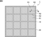
- FIG. 1 is an exploded perspective view showing a schematic example of a substrate for producing a capacitor element according to a first embodiment of the present invention.
- FIG. 2 is a plan view of the substrate for producing a capacitor element shown in FIG.
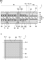
- FIG. 3 is a cross-sectional view that illustrates an example of a substrate for producing a capacitor element according to the first embodiment of the present invention.
- 4A and 4B are plan and cross-sectional views each showing an example of an arrangement of the through-holes in the outside-of-product region;
- 5A and 5B are plan and cross-sectional views each showing a schematic example of an arrangement of the through-holes in the outside-of-product region;
- FIG. 6A is a cross-sectional view that shows a schematic example of a process for separating a product region R1 from a capacitor element manufacturing substrate 1.
- Fig. 6B is a plan view that shows a schematic example of a process for separating a product region R1 from a capacitor element manufacturing substrate 1.
- Fig. 7A is a cross-sectional view that typically shows one example of a capacitor element obtained from the capacitor element production substrate 1.
- Fig. 7B is a plan view that typically shows one example of a capacitor element obtained from the capacitor element production substrate 1.
- FIG. 8 is a cross-sectional view that typically shows a first modified example of the capacitor element production substrate 1 shown in FIG. FIG.
- FIG. 9 is a cross-sectional view that typically shows a second modified example of the capacitor element production substrate 1 shown in FIG.
- FIG. 10 is a cross-sectional view that illustrates an example of a substrate for producing a capacitor element according to the second embodiment of the present invention.
- FIG. 11 is a cross-sectional view that illustrates a schematic diagram of another example of a substrate for producing a capacitor element according to the second embodiment of the present invention.
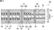
- FIG. 12 is a cross-sectional view that typically shows a modified example of the capacitor element production substrate 2 shown in FIG.
- FIG. 13 is a cross-sectional view that typically shows a modified example of the capacitor element production substrate 2' shown in FIG. FIG.
- FIG. 14 is a cross-sectional view that illustrates an example of a substrate for producing a capacitor element according to the third embodiment of the present invention.
- FIG. 15 is a cross-sectional view that illustrates a schematic diagram of another example of a substrate for producing a capacitor element according to the third embodiment of the present invention.
- FIG. 16 is a cross-sectional view that typically shows a modified example of the capacitor element production substrate 3 shown in FIG.
- FIG. 17 is a cross-sectional view that typically shows a modified example of the capacitor element production substrate 3' shown in FIG.
- terms indicating the relationship between elements e.g., "perpendicular,” “parallel,” “orthogonal,” etc.
- terms indicating the shapes of elements are not expressions that express only a strict meaning, but are expressions that include a range of substantial equivalence, for example, differences of about a few percent.
- Fig. 1 is an exploded perspective view showing a schematic example of a substrate for producing a capacitor element according to a first embodiment of the present invention.
- Fig. 2 is a plan view of the substrate for producing a capacitor element shown in Fig. 1.
- a first external electrode layer 91 and a second external electrode layer 92 which will be described later, are omitted in Figs. 1 and 2.
- the capacitor element manufacturing substrate 1 shown in Figures 1 and 2 comprises a substrate layer 10 and a sealing layer 20 arranged to cover at least one of the main surfaces of the substrate layer 10.
- the sealing layer 20 is provided so as to cover both opposing main surfaces in the thickness direction of the substrate layer 10.
- the substrate layer 10 is protected by the sealing layer 20.
- the sealing layer 20 may be composed of only one layer on one main surface side of the substrate layer 10, or may be composed of two or more layers. When the sealing layer 20 is composed of two or more layers, the materials constituting each layer may be the same or different.
- the sealing layer 20 is formed to seal the substrate layer 10, for example, by a method of thermocompressing an insulating resin sheet, or by applying an insulating resin paste and then thermally curing it.
- the substrate layer 10 is divided into a product region R1 and an outside-product region R2 that surrounds at least a portion of the product region R1.
- the capacitor element manufacturing substrate 1 is a semi-finished product. As described below, the product region R1 is separated from the capacitor element manufacturing substrate 1 to produce a capacitor element (for example, the capacitor element 100 shown in Figures 7A and 7B), which is a final product (finished product).
- a capacitor element for example, the capacitor element 100 shown in Figures 7A and 7B
- Product region R1 is the region that constitutes the capacitor element, which is the final product (finished product). There is no particular limit to the number of product regions R1 included in substrate layer 10, and there may be one or more.
- the product regions R1 may be arranged regularly or irregularly.
- the sizes and planar shapes of the product regions R1 may be the same, or some or all of them may be different.
- each product area R1 Although not shown in Figures 1 and 2, one or more capacitor units are arranged in each product area R1.
- the number of capacitor units arranged in each product area R1 may be the same, or some or all of them may be different.
- the capacitor sections may be arranged regularly or irregularly.
- the size and planar shape of the capacitor sections may be the same, or some or all of them may be different. It is preferable that the capacitor sections have the same configuration, but capacitor sections with different configurations may be included.
- the outside-product area R2 is arranged to surround the entire product area R1.
- the planar shape of the product area R1 is rectangular (i.e., square or oblong)
- the outside-product area R2 may be arranged to surround two opposing sides of the product area R1, may be arranged in an L-shape to surround two adjacent sides of the product area R1, or may be arranged in a frame shape to surround the four sides of the product area R1.
- FIG. 3 is a cross-sectional view showing a schematic example of a substrate for manufacturing capacitor elements according to the first embodiment of the present invention. Note that FIG. 3 is a cross-sectional view taken along line III-III of the substrate for manufacturing capacitor elements shown in FIG. 2.
- Product region R1 includes an anode plate 11 having a porous portion 11B on at least one main surface of a core portion 11A, a dielectric layer 13 provided on the surface of the porous portion 11B, and a cathode layer 12 provided on the surface of the dielectric layer 13. This makes up an electrolytic capacitor.
- the anode plate 11 has a porous portion 11B on both main surfaces of the core portion 11A, but it may also have a porous portion 11B on only one of the main surfaces of the core portion 11A.
- the capacitor section is formed by the anode plate 11, the dielectric layer 13, and the cathode layer 12.
- the cathode layer 12 includes, for example, a solid electrolyte layer 12A provided on the surface of the dielectric layer 13. It is preferable that the cathode layer 12 further includes a conductor layer 12B provided on the surface of the solid electrolyte layer 12A.
- the product region R1 constitutes a solid electrolytic capacitor.
- the outside-product region R2 includes the core 11A of the anode plate 11. As shown in FIG. 3, the outside-product region R2 may include an anode plate 11 having a porous portion 11B on at least one main surface of the core portion 11A, and may further include a dielectric layer 13 provided on the surface of the porous portion 11B.
- the outside-product area R2 is an area that does not function as a capacitor element in the final product, or is an area that is not used as a capacitor element in the final product. In the capacitor element in the final product, the outside-product area R2 may be completely removed, or a portion of the outside-product area R2 may remain.
- the anode To function as a capacitor element, the anode must be connected to the core 11A of the anode plate 11, and the cathode must be connected to the cathode layer 12. Therefore, the area where the anode is not connected to the core 11A of the anode plate 11 or the area where the cathode is not connected to the cathode layer 12 corresponds to the outside product area R2 that does not function as a capacitor element.
- the region does not function as a capacitor element in the final product and falls under the outside-product region R2. Also, even if there is a region in which a through-hole conductor electrically connected to the anode plate 11 and a through-hole conductor electrically connected to the cathode layer 12 are provided at the stage of the semi-finished capacitor element manufacturing substrate 1, the region that is removed before the final product falls under the outside-product region R2.
- a through-hole 30 is provided that penetrates the anode plate 11 in the thickness direction.
- the number of through-holes 30 is not particularly limited and may be one or more.
- the product outside region R2 in which the through-hole 30 is provided may include at least a portion of the region located on the outer edge of the substrate layer 10. Therefore, the through-hole 30 may be provided in a portion of the region located on the outer edge of the substrate layer 10, or the through-hole 30 may be provided in the entire region located on the outer edge of the substrate layer 10.
- the through-holes 30 may be holes that penetrate the anode plate 11 in the thickness direction, or may be grooves that divide the anode plate 11 in the thickness direction.
- the through-holes 30 may be a mixture of holes that penetrate the anode plate 11 in the thickness direction and grooves that divide the anode plate 11 in the thickness direction.
- the width of the through-hole 30 may be constant in the thickness direction, may decrease in the thickness direction, or may increase in the thickness direction. Also, the width of the through-hole 30 may be smaller at the center side of the anode plate 11 than at both main surfaces, or may be larger at the center side of the anode plate 11 than at both main surfaces.
- At least a portion of the through-hole 30 is filled with the filling member 40.
- the entire through-hole 30 is filled with the filling member 40, but only a portion of the through-hole 30 may be filled with the filling member 40.
- the filling member 40 includes an insulating member.
- the insulating member includes a sealing layer 20 that penetrates the through-hole 30.
- the sealing layer 20 only needs to penetrate at least a portion of the through-hole 30, and may penetrate the entire through-hole 30.
- the filling member 40 is preferably in contact with the sealing layer 20 on at least one main surface side of the substrate layer 10, and is preferably in contact with the sealing layer 20 on both main surface sides of the substrate layer 10.
- the filling member 40 may be integral with the sealing layer 20 on at least one main surface side of the substrate layer 10, or may be integral with the sealing layer 20 on both main surface sides of the substrate layer 10.
- a through-hole 30 may be provided in at least a portion of the outside-product region R2 that is located between adjacent product regions R1. In this case, it is preferable that at least a portion of the through-hole 30 is filled with the filling member 40.
- a dummy electrode layer 50 may be provided on the surface of the sealing layer 20.
- one dummy electrode layer 50 may be provided for the outside-product region R2, or multiple dummy electrode layers 50 may be provided.
- the dummy electrode layer 50 may be provided on the surface of the sealing layer 20 on both main surface sides, or on the surface of the sealing layer 20 on one of the main surface sides.
- the dummy electrode layer 50 may extend to the product region R1. In the outside-product region R2, the dummy electrode layer 50 may not be provided on the surface of the sealing layer 20.
- the dummy electrode layer 50 is an example of a dummy layer.
- the dummy layer may be a conductive layer like an electrode layer, or may be an insulating layer like an insulating layer.
- a dummy layer such as a dummy electrode layer 50 is provided in the outside-product region R2
- both ends of the through-hole 30 are covered by the dummy electrode layer 50, but either one end of the through-hole 30 may be covered by the dummy electrode layer 50.
- the configuration of the dummy electrode layer 50 is preferably the same as that of the first external electrode layer 91 and the second external electrode layer 92 described below.
- an insulating layer 15 may be provided between the anode plate 11 and the sealing layer 20.
- the insulating layer 15 may be provided between the sealing layer 20 on one of the main surfaces and the anode plate 11, or the insulating layer 15 may be provided between the sealing layer 20 on both main surfaces and the anode plate 11.
- the insulating layer 15 may be composed of only one layer, or may be composed of two or more layers. When the insulating layer 15 is composed of two or more layers, the materials constituting each layer may be the same or different.
- the insulating layer 15 includes a first insulating layer 15A provided on the surface of the dielectric layer 13 and a second insulating layer 15B provided on the surface of the first insulating layer 15A.
- the thickness of the first insulating layer 15A may be the same as the thickness of the second insulating layer 15B, may be greater than the thickness of the second insulating layer 15B, or may be smaller than the thickness of the second insulating layer 15B.
- the product region R1 may include a first through-hole conductor 61 that is arranged to penetrate the anode plate 11 and the sealing layer 20 in the thickness direction and is electrically connected to the anode plate 11.
- the first through-hole conductor 61 only needs to be provided on at least the inner wall surface of the first through hole 71 that penetrates the anode plate 11 and the sealing layer 20 in the thickness direction.
- the first through-hole conductor 61 may be provided only on the inner wall surface of the first through hole 71, or may be provided throughout the entire interior of the first through hole 71.
- one first through-hole conductor 61 may be provided inside the cathode layer 12 included in each capacitor portion, or two or more first through-hole conductors 61 may be provided.
- the end face of the cathode layer 12 and the first through-hole conductor 61 are insulated by an insulating material (insulating layer 15 in FIG. 3).
- the first through-hole conductor 61 is electrically connected to the anode plate 11 on the inner wall surface of the first through hole 71.
- a first resin filling portion 81 filled with a resin material may be provided inside the first through-hole conductor 61.
- the first resin filling portion 81 is provided in the space surrounded by the first through-hole conductor 61 in the first through hole 71.
- the first resin filling portion 81 may be a conductor or an insulator.
- the product region R1 may include a second through-hole conductor 62 that is arranged to penetrate the anode plate 11 and the sealing layer 20 in the thickness direction and is electrically connected to the cathode layer 12.
- the second through-hole conductor 62 may be provided at least on the inner wall surface of the second through hole 72 that penetrates the anode plate 11 and the sealing layer 20 in the thickness direction.
- the second through-hole conductor 62 may be provided only on the inner wall surface of the second through hole 72, or may be provided throughout the entire interior of the second through hole 72.
- one second through-hole conductor 62 may be provided inside the cathode layer 12 included in each capacitor section, or two or more second through-hole conductors 62 may be provided.
- the number of second through-hole conductors 62 may be the same as the number of first through-hole conductors 61, or may be different.
- the end face of the anode plate 11 and the second through-hole conductor 62 are insulated by an insulating material (part of the sealing layer 20 in FIG. 3).
- a second resin filling portion 82 filled with a resin material may be provided inside the second through-hole conductor 62.
- the second resin filling portion 82 is provided in the space surrounded by the second through-hole conductor 62 in the second through hole 72.
- the second resin filling portion 82 may be a conductor or an insulator.
- first through-hole conductor 61 or the second through-hole conductor 62 is provided inside the sealing layer 20, it is preferable that an insulating layer 15 is provided around the first through-hole conductor 61 or the second through-hole conductor 62 on at least one of the main surfaces of the anode plate 11.
- an insulating layer 15 may be provided on at least one of the main surfaces of the anode plate 11 so as to surround the periphery of the cathode layer 12.
- the insulating layer 15 may be provided so as to surround a portion of the periphery of the cathode layer 12, but it is preferable that the insulating layer 15 is provided so as to surround the entire periphery of the cathode layer 12.
- the product region R1 may include a third through-hole conductor that is arranged to penetrate the anode plate 11 and the sealing layer 20 in the thickness direction and is not electrically connected to the anode plate 11 and the cathode layer 12.
- the product region R1 may include a first external electrode layer 91 provided on the surface of the sealing layer 20 and electrically connected to the anode plate 11 and the first through-hole conductor 61.
- the first external electrode layer 91 may extend to the outside-product region R2.
- one first external electrode layer 91 may be provided, or multiple first external electrode layers 91 may be provided.
- the planar shape of the first external electrode layer 91 when viewed from the thickness direction is not particularly limited, and examples include a rectangle (square or oblong), a quadrangle other than a rectangle, a polygon such as a triangle, a pentagon, or a hexagon, a circle, an ellipse, or a combination of these.
- the planar shape of the first external electrode layer 91 may be an L-shape, a C-shape, a stepped shape, or the like.
- the product region R1 may include a second external electrode layer 92 provided on the surface of the sealing layer 20 and electrically connected to the cathode layer 12 and the second through-hole conductor 62.
- the second external electrode layer 92 may extend to the outside-product region R2.
- one second external electrode layer 92 may be provided, or multiple second external electrode layers 92 may be provided.
- the number of second external electrode layers 92 may be the same as the number of first external electrode layers 91, or may be different.
- the planar shape of the second external electrode layer 92 when viewed from the thickness direction is not particularly limited, and examples include a rectangle (square or rectangle), a quadrangle other than a rectangle, a polygon such as a triangle, a pentagon, or a hexagon, a circle, an ellipse, or a combination of these.
- the planar shape of the second external electrode layer 92 may also be an L-shape, a C-shape, a stepped shape, or the like.
- the planar shape of the second external electrode layer 92 when viewed from the thickness direction may be the same as or different from the planar shape of the first external electrode layer 91 when viewed from the thickness direction.
- the product region R1 may include a via conductor arranged to penetrate the sealing layer 20 in the thickness direction.
- the product region R1 may include a via conductor electrically connected to the anode plate 11.
- the anode plate 11 is electrically led out to the outside of the sealing layer 20 through the via conductor, and can be electrically connected to the outside of the sealing layer 20.
- the product region R1 may include a via conductor electrically connected to the cathode layer 12.
- the cathode layer 12 is electrically led out to the outside of the sealing layer 20 through the via conductor, and can be electrically connected to the outside of the sealing layer 20.
- FIG. 4A is a plan view showing a schematic example of the arrangement of the penetration parts in the area outside the product.
- FIG. 4B is a cross-sectional view showing a schematic example of the arrangement of the penetration parts in the area outside the product. Note that FIG. 4A is a plan view taken along line A-A in FIG. 4B.
- At least three penetrations 30 are arranged at equal intervals in the outside-product region R2 (see Figure 3, etc.).
- "Equal intervals” here does not mean only in the strict sense, but also means that the range is substantially the same, for example, including a difference of about a few percent.
- At least three penetrations 30 By arranging at least three penetrations 30 at equal intervals, localized stress concentration is prevented, thereby suppressing delamination. Note that as long as at least three penetrations 30 are arranged at equal intervals, penetrations 30 with different intervals may be included.
- the distance between the evenly spaced through-holes 30 (the length indicated by the arrows in FIG. 4A) is not particularly limited, but is preferably 1 mm or less. On the other hand, the distance between the evenly spaced through-holes 30 is, for example, 0.1 mm or more.
- FIG. 5A is a plan view showing a schematic example of another arrangement of the penetration parts in the area outside the product.
- FIG. 5B is a cross-sectional view showing a schematic example of another arrangement of the penetration parts in the area outside the product. Note that FIG. 5A is a plan view taken along line A-A in FIG. 5B.
- At least three through-holes 30 are arranged at equal intervals in the outside-product region R2 (see Figure 3, etc.), and it is preferable that at least two of the evenly spaced through-holes 30 have the same planar shape when viewed from the thickness direction. In particular, it is preferable that all of the evenly spaced through-holes 30 have the same planar shape.
- the phrase "same planar shape" used here does not only have a strict meaning, but also includes a substantially equivalent range, for example, a difference of about a few percent.
- FIG. 6A is a cross-sectional view that shows a schematic example of a process for separating a product region R1 from a substrate 1 for manufacturing capacitor elements.
- FIG. 6B is a plan view that shows a schematic example of a process for separating a product region R1 from a substrate 1 for manufacturing capacitor elements.
- the product region R1 is separated by removing the outside-product region R2 from the capacitor element manufacturing substrate 1.
- the entire outside-product region R2 may be removed by cutting the capacitor element manufacturing substrate 1 at the position of the cutting line CL1.
- a portion of the outside-product region R2 may be removed by cutting the capacitor element manufacturing substrate 1 at the position of the cutting line CL1a.
- FIG. 7A is a cross-sectional view that shows a schematic example of a capacitor element obtained from a substrate 1 for manufacturing capacitor elements.
- FIG. 7B is a plan view that shows a schematic example of a capacitor element obtained from a substrate 1 for manufacturing capacitor elements.
- FIG. 8 is a cross-sectional view that shows a schematic diagram of a first modified example of the capacitor element manufacturing substrate 1 shown in FIG. 3.
- the sealing layer 20 includes a first sealing layer 21 provided to cover at least one of the main surfaces of the substrate layer 10, and a second sealing layer 22 provided on the surface of the first sealing layer 21.
- the filling member 40 includes an insulating member.
- the insulating member includes a second sealing layer 22 that penetrates the through-hole 30.
- the second sealing layer 22 may penetrate at least a portion of the through-hole 30, or may penetrate the entire through-hole 30.
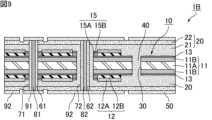
- FIG. 9 is a cross-sectional view that shows a schematic diagram of a second modified example of the capacitor element manufacturing substrate 1 shown in FIG. 3.
- the sealing layer 20 includes a first sealing layer 21 provided to cover at least one of the main surfaces of the substrate layer 10, and a second sealing layer 22 provided on the surface of the first sealing layer 21.
- the filling member 40 includes an insulating member.
- the insulating member includes a first sealing layer 21 that penetrates the through-hole 30.
- the first sealing layer 21 only needs to penetrate at least a portion of the through-hole 30, and may penetrate the entire through-hole 30.
- the adhesion between the first sealing layer 21 and the second sealing layer 22 in the outside-product region R2 can be improved by filling at least a portion of the penetration portion 30 with a filling member 40. Therefore, swelling due to delamination in the outside-product region R2 can be suppressed. This also makes it possible to suppress swelling in the product region R1.
- the filling member includes a conductive member.
- FIG. 10 is a cross-sectional view showing a schematic example of a substrate for manufacturing capacitor elements according to the second embodiment of the present invention.
- the filling member 40 includes a conductive member 41.
- the conductive member 41 needs to be provided at least on the inner wall surface of the through-hole 30.
- the conductive member 41 may be provided only on the inner wall surface of the through-hole 30, or may be provided throughout the entire interior of the through-hole 30.
- the conductive member 41 may be in contact with the anode plate 11 on the inner wall surface of the through portion 30.
- a resin-filled portion 45 filled with a resin material may be provided inside the conductive member 41.
- the resin-filled portion 45 is provided in the space surrounded by the conductive member 41 inside the through-hole 30.
- the resin-filled portion 45 may be a conductor or an insulator.
- the configuration of the conductive member 41 is the same as that of the first through-hole conductor 61 and the second through-hole conductor 62.
- a dummy electrode layer 50 may be provided on the surface of the sealing layer 20.
- a dummy layer such as a dummy electrode layer 50 is provided in the outside-product region R2
- both ends of the through-hole 30 are covered by the dummy electrode layer 50, but either one end of the through-hole 30 may be covered by the dummy electrode layer 50.
- the conductive member 41 included in the filling member 40 is connected to the dummy electrode layer 50. In this case, delamination is further suppressed.
- FIG. 11 is a cross-sectional view showing a schematic diagram of another example of a substrate for manufacturing capacitor elements according to the second embodiment of the present invention.
- the filling member 40 further includes an insulating member 42 located outside the conductive member 41.
- the filling member 40 may be composed of two or more layers of members extending inward from the inner wall surface of the through portion 30.
- the insulating member 42 includes a sealing layer 20 that penetrates the through-hole 30.
- the sealing layer 20 needs to penetrate at least a portion of the space between the anode plate 11 and the conductive member 41, and may penetrate entirely between the anode plate 11 and the conductive member 41.
- the insulating member 42 is preferably in contact with the sealing layer 20 on at least one main surface side of the substrate layer 10, and is preferably in contact with the sealing layer 20 on both main surface sides of the substrate layer 10.
- the insulating member 42 may be integral with the sealing layer 20 on at least one main surface side of the substrate layer 10, or may be integral with the sealing layer 20 on both main surface sides of the substrate layer 10.
- the filling member 40 includes an insulating member 42, so delamination is further suppressed compared to the capacitor element manufacturing substrate 2 shown in FIG. 10.
- FIG. 12 is a cross-sectional view that shows a schematic diagram of a modified example of the capacitor element manufacturing substrate 2 shown in FIG. 10.
- the sealing layer 20 may include a first sealing layer 21 provided to cover at least one of the main surfaces of the substrate layer 10, and a second sealing layer 22 provided on the surface of the first sealing layer 21.
- FIG. 13 is a cross-sectional view that shows a schematic diagram of a modified example of the capacitor element manufacturing substrate 2' shown in FIG. 11.
- the sealing layer 20 may include a first sealing layer 21 provided to cover at least one of the main surfaces of the substrate layer 10, and a second sealing layer 22 provided on the surface of the first sealing layer 21.
- the insulating member 42 includes a first sealing layer 21 that penetrates into the through-hole 30.
- the first sealing layer 21 may penetrate at least partially between the anode plate 11 and the conductive member 41, or may penetrate entirely between the anode plate 11 and the conductive member 41.
- the outside area of the product includes an anode plate having a porous portion on at least one main surface of a core portion, a dielectric layer provided on the surface of the porous portion, and a cathode layer provided on the surface of the dielectric layer.
- FIG. 14 is a cross-sectional view showing a schematic example of a substrate for manufacturing capacitor elements according to the third embodiment of the present invention.
- the outside-product region R2 includes an anode plate 11 having a porous portion 11B on at least one main surface of a core portion 11A, a dielectric layer 13 provided on the surface of the porous portion 11B, and a cathode layer 12 provided on the surface of the dielectric layer 13.
- the configuration of the cathode layer 12 provided in the outside product region R2 is the same as that of the cathode layer 12 provided in the product region R1.
- an insulating layer 15 may be provided between the anode plate 11 and the sealing layer 20.
- the penetration portion 30 penetrates the anode plate 11 and the insulating layer 15 in the thickness direction.
- the insulating layer 15 may be provided between the sealing layer 20 on one of the main surfaces and the anode plate 11, or between the sealing layer 20 on both main surfaces and the anode plate 11.
- the insulating layer 15 may be composed of only one layer, or may be composed of two or more layers. When the insulating layer 15 is composed of two or more layers, the materials constituting each layer may be the same or different.
- the insulating layer 15 includes a first insulating layer 15A provided on the surface of the dielectric layer 13, and a second insulating layer 15B provided on the surface of the first insulating layer 15A.
- the thickness of the first insulating layer 15A may be the same as the thickness of the second insulating layer 15B, may be greater than the thickness of the second insulating layer 15B, or may be smaller than the thickness of the second insulating layer 15B.
- the insulating layer 15 in the product outer region R2 is preferably provided around the through-hole 30. Also, in the product outer region R2, the insulating layer 15 may be provided so as to surround the cathode layer 12.
- the configuration of the insulating layer 15 provided in the outside-product region R2 is preferably the same as that of the insulating layer 15 provided in the product region R1. Note that the insulating layer 15 may not be provided in the product region R1, and may be provided only in the outside-product region R2. The configuration of the insulating layer 15 provided in the outside-product region R2 may be in contact with the insulating layer 15 provided in the product region R1, or may be separated from the insulating layer 15 provided in the product region R1.
- the outside-product region R2 has a common configuration with the product region R1, the difference in thickness of the sealing layer 20 between the product region R1 and the outside-product region R2 is reduced. This reduces the generation of stress due to undulations in the substrate.
- the filling material 40 it is possible to reduce swelling due to delamination in the outside-product region R2.
- FIG. 15 is a cross-sectional view showing a schematic diagram of another example of a substrate for manufacturing a capacitor element according to the third embodiment of the present invention.
- the outside-product region R2 includes an anode plate 11 having a porous portion 11B on at least one main surface of a core portion 11A, a dielectric layer 13 provided on the surface of the porous portion 11B, and a cathode layer 12 provided on the surface of the dielectric layer 13.
- an insulating layer 15 may be provided between the anode plate 11 and the sealing layer 20.
- the penetration portion 30 penetrates the anode plate 11 and the insulating layer 15 in the thickness direction.
- the insulating layer 15 may be provided between the sealing layer 20 on one of the main surfaces and the anode plate 11, or between the sealing layer 20 on both main surfaces and the anode plate 11.
- FIG. 16 is a cross-sectional view that shows a schematic diagram of a modified example of the capacitor element manufacturing substrate 3 shown in FIG. 14.
- the sealing layer 20 may include a first sealing layer 21 provided to cover at least one of the main surfaces of the substrate layer 10, and a second sealing layer 22 provided on the surface of the first sealing layer 21.
- FIG. 17 is a cross-sectional view that shows a schematic diagram of a modified example of the capacitor element manufacturing substrate 3' shown in FIG. 15.
- the sealing layer 20 may include a first sealing layer 21 provided to cover at least one of the main surfaces of the substrate layer 10, and a second sealing layer 22 provided on the surface of the first sealing layer 21.
- the insulating member 42 includes a first sealing layer 21 that penetrates the through-hole 30.
- the first sealing layer 21 may penetrate at least partially between the anode plate 11 and the conductive member 41, or may penetrate entirely between the anode plate 11 and the conductive member 41.
- the substrate for manufacturing capacitor elements of the present invention is not limited to the above-described embodiment, and various applications and modifications can be made within the scope of the present invention with respect to the configuration of the product area and non-product area, manufacturing conditions, etc.
- an insulating layer may be provided between the anode plate and the sealing layer in the outside-product area, as in the third embodiment.
- the penetration portion penetrates the anode plate and the insulating layer in the thickness direction.
- the insulating layer in the area outside the product is preferably provided around the penetration portion. Also, in the area outside the product, the insulating layer may be provided so as to surround the cathode layer.
- penetrations filled with the filling material described in the different embodiments may be mixed in.
- the planar shape of the capacitor portion when viewed from the thickness direction may be, for example, a rectangle (square or oblong), a quadrangle other than a rectangle, a polygon such as a triangle, a pentagon, or a hexagon, a circle, an ellipse, or a combination of these.
- the planar shape of the capacitor portion may also be an L-shape, a C-shape, a stepped shape, etc.
- the anode plate 11 is preferably made of a valve metal that exhibits so-called valve action.
- valve metals include simple metals such as aluminum, tantalum, niobium, titanium, and zirconium, or alloys containing at least one of these metals. Of these, aluminum or an aluminum alloy is preferred.
- the shape of the anode plate 11 is preferably flat, and more preferably foil-like.
- plate-like includes “foil-like”.
- the anode plate 11 may have a porous portion 11B on at least one of the main surfaces of the core portion 11A.
- the anode plate 11 may have a porous portion 11B on only one of the main surfaces of the core portion 11A, or may have a porous portion 11B on both main surfaces of the core portion 11A.
- the porous portion 11B is preferably a porous layer formed on the surface of the core portion 11A, and is more preferably an etched layer.
- the thickness of the anode plate 11 before the etching process is preferably 60 ⁇ m or more and 200 ⁇ m or less.
- the thickness of the unetched core portion 11A after the etching process is preferably 15 ⁇ m or more and 70 ⁇ m or less.
- the thickness of the porous portion 11B is designed according to the required withstand voltage and electrostatic capacitance, but it is preferable that the combined thickness of the porous portions 11B on both sides of the core portion 11A is 10 ⁇ m or more and 180 ⁇ m or less.
- the pore diameter of the porous portion 11B is preferably 10 nm or more and 600 nm or less.
- the pore diameter of the porous portion 11B means the median diameter D50 measured by a mercury porosimeter.
- the pore diameter of the porous portion 11B can be controlled, for example, by adjusting various etching conditions.
- the dielectric layer 13 provided on the surface of the porous portion 11B is porous, reflecting the surface condition of the porous portion 11B, and has a finely uneven surface shape.
- the dielectric layer 13 is preferably made of an oxide film of the valve metal.
- the dielectric layer 13 made of an oxide film can be formed by anodizing the surface of the aluminum foil in an aqueous solution containing ammonium adipate or the like (also called chemical conversion treatment).
- the thickness of the dielectric layer 13 is designed according to the required withstand voltage and capacitance, but is preferably 10 nm or more and 100 nm or less.
- the cathode layer 12 includes a solid electrolyte layer 12A
- examples of materials constituting the solid electrolyte layer 12A include conductive polymers such as polypyrroles, polythiophenes, and polyanilines. Among these, polythiophenes are preferred, and poly(3,4-ethylenedioxythiophene), also known as PEDOT, is particularly preferred.
- the conductive polymer may also include a dopant such as polystyrene sulfonate (PSS).
- PSS polystyrene sulfonate
- the solid electrolyte layer 12A preferably includes an inner layer that fills the pores (recesses) of the dielectric layer 13, and an outer layer that covers the dielectric layer 13.
- the thickness of the solid electrolyte layer 12A from the surface of the porous portion 11B is preferably 2 ⁇ m or more and 20 ⁇ m or less.
- the solid electrolyte layer 12A is formed, for example, by a method of forming a polymerized film of poly(3,4-ethylenedioxythiophene) or the like on the surface of the dielectric layer 13 using a treatment liquid containing a monomer such as 3,4-ethylenedioxythiophene, or by applying a dispersion of a polymer such as poly(3,4-ethylenedioxythiophene) to the surface of the dielectric layer 13 and drying it.
- the solid electrolyte layer 12A can be formed in a predetermined area by applying the above-mentioned treatment liquid or dispersion liquid to the surface of the dielectric layer 13 by a method such as sponge transfer, screen printing, dispenser application, or inkjet printing.
- the conductor layer 12B includes at least one of a conductive resin layer and a metal layer.
- the conductor layer 12B may be only a conductive resin layer or only a metal layer. It is preferable that the conductor layer 12B covers the entire surface of the solid electrolyte layer 12A.
- the conductive resin layer may be, for example, a conductive adhesive layer containing at least one conductive filler selected from the group consisting of silver filler, copper filler, nickel filler, and carbon filler.
- the metal layer examples include metal plating films and metal foils.
- the metal layer is preferably made of at least one metal selected from the group consisting of nickel, copper, silver, and alloys containing these metals as the main components.
- the term "main component" refers to the elemental component with the largest weight ratio.
- the conductive layer 12B includes, for example, a carbon layer provided on the surface of the solid electrolyte layer 12A and a copper layer provided on the surface of the carbon layer.
- the carbon layer is provided to electrically and mechanically connect the solid electrolyte layer 12A and the copper layer.
- the carbon layer can be formed in a predetermined area by applying carbon paste to the surface of the solid electrolyte layer 12A by sponge transfer, screen printing, dispenser application, inkjet printing, or other methods.
- the thickness of the carbon layer is preferably 2 ⁇ m or more and 20 ⁇ m or less.
- the copper layer can be formed in a predetermined area by applying copper paste to the surface of the carbon layer by sponge transfer, screen printing, spray application, dispenser application, inkjet printing, or other methods.
- the thickness of the copper layer is preferably 2 ⁇ m or more and 20 ⁇ m or less.
- the sealing layer 20 is made of an insulating material. In this case, it is preferable that the sealing layer 20 contains an insulating resin.
- Examples of insulating resins contained in the sealing layer 20 include epoxy resins, phenolic resins, etc.
- the sealing layer 20 further contains a filler.
- Examples of the filler contained in the sealing layer 20 include inorganic fillers such as silica particles and alumina particles.
- a layer such as a stress relief layer or a moisture-proof film may be provided between the anode plate 11 and the sealing layer 20.
- the insulating layer 15 is made of an insulating material. In this case, it is preferable that the insulating layer 15 is made of an insulating resin.
- Examples of insulating resins constituting the insulating layer 15 include polyphenylsulfone resin, polyethersulfone resin, cyanate ester resin, fluororesin (tetrafluoroethylene, tetrafluoroethylene-perfluoroalkylvinylether copolymer, etc.), polyimide resin, polyamideimide resin, epoxy resin, and derivatives or precursors thereof.
- the insulating layer 15 may be made of the same resin as the sealing layer 20. Unlike the sealing layer 20, if the insulating layer 15 contains inorganic filler, this may adversely affect the effective capacitance part of the capacitor, so it is preferable that the insulating layer 15 is made of a resin alone.
- the insulating layer 15 can be formed in a predetermined area by applying a mask material, such as a composition containing an insulating resin, to the surface of the porous portion 11B by a method such as sponge transfer, screen printing, dispenser application, or inkjet printing.
- a mask material such as a composition containing an insulating resin
- the insulating layer 15 may be formed on the porous portion 11B either before the dielectric layer 13 or after the dielectric layer 13.
- the first external electrode layer 91 is electrically connected to the anode plate 11.
- the first external electrode layer 91 is provided on the surface of the first through-hole conductor 61, and functions as a connection terminal for the capacitor section.
- the first external electrode layer 91 is electrically connected to the anode plate 11 via the first through-hole conductor 61, and functions as a connection terminal for the anode plate 11.
- the constituent material of the first external electrode layer 91 examples include metal materials containing low-resistance metals such as silver, gold, and copper.
- the first external electrode layer 91 is formed, for example, by plating the surface of the first through-hole conductor 61.
- a mixed material of at least one conductive filler selected from the group consisting of silver filler, copper filler, nickel filler, and carbon filler, and resin may be used as the constituent material of the first external electrode layer 91.
- the second external electrode layer 92 is electrically connected to the cathode layer 12.
- the second external electrode layer 92 is provided on the surface of the second through-hole conductor 62 and functions as a connection terminal of the capacitor section.
- the second external electrode layer 92 may be made of a metal material containing a low-resistance metal such as silver, gold, or copper.
- the second external electrode layer 92 is formed by, for example, plating the surface of the second through-hole conductor 62.
- a mixed material of at least one conductive filler selected from the group consisting of silver filler, copper filler, nickel filler, and carbon filler and resin may be used as the constituent material of the second external electrode layer 92.
- the constituent materials of the first external electrode layer 91 and the second external electrode layer 92 are preferably the same as each other at least in terms of type, but may be different from each other.
- each capacitor section may be provided with a first external electrode layer 91 electrically connected to the anode plate 11 and a second external electrode layer 92 electrically connected to the cathode layer 12, and at least one of the first external electrode layer 91 and the second external electrode layer 92 may be provided in common among the multiple capacitor sections.
- the first external electrode layer 91 and the second external electrode layer 92 may be provided on both main surfaces of the sealing layer 20, or may be provided on only one main surface of the sealing layer 20.
- the first through-hole conductor 61 When the first through-hole conductor 61 is electrically connected to the anode plate 11 on the inner wall surface of the first through hole 71, it is preferable that the first through-hole conductor 61 is electrically connected to the end surface of the anode plate 11 that faces the inner wall surface of the first through hole 71 in the surface direction. As a result, the anode plate 11 is electrically led out to the outside via the first through-hole conductor 61.
- the core portion 11A and the porous portion 11B are exposed on the end face of the anode plate 11 that is electrically connected to the first through-hole conductor 61.
- the porous portion 11B as well as the core portion 11A are electrically connected to the first through-hole conductor 61.
- the first through-hole conductor 61 is electrically connected to the anode plate 11 around the entire circumference of the first through hole 71.
- the connection resistance between the anode plate 11 and the first through-hole conductor 61 tends to decrease, and therefore the equivalent series resistance (ESR) tends to decrease.
- the second through-hole conductor 62 is electrically connected to the cathode layer 12, for example, via the second external electrode layer 92 and the via conductor.
- the first through-hole conductor 61 is formed, for example, as follows. First, a first through hole 71 is formed by drilling, laser processing, or the like, penetrating the anode plate 11 and the sealing layer 20 in the thickness direction. Then, the inner wall surface of the first through hole 71 is metallized with a metal material containing a low-resistance metal such as copper, gold, or silver, to form the first through-hole conductor 61. When forming the first through-hole conductor 61, for example, the inner wall surface of the first through hole 71 is metallized with an electroless copper plating process, an electrolytic copper plating process, or the like, to facilitate processing.
- a metal material containing a low-resistance metal such as copper, gold, or silver
- the method of forming the first through-hole conductor 61 may be a method of filling the first through hole 71 with a metal material, a composite material of metal and resin, or the like, in addition to a method of metallizing the inner wall surface of the first through hole 71.
- An anode connection layer may be provided between the anode plate 11 and the first through-hole conductor 61 in the surface direction.
- the anode plate 11 and the first through-hole conductor 61 may be electrically connected via the anode connection layer.
- the anode connection layer functions as a barrier layer for the anode plate 11, more specifically, as a barrier layer for the core portion 11A and the porous portion 11B.
- the anode connection layer functions as a barrier layer for the anode plate 11
- dissolution of the anode plate 11 that occurs during chemical treatment to form external electrode layers such as the first external electrode layer 91 is suppressed, and thus the infiltration of the chemical solution into the capacitor portion is suppressed, which tends to improve reliability.
- the anode connection layer preferably includes a layer mainly composed of nickel. In this case, damage to the metal (e.g., aluminum) constituting the anode plate 11 is reduced, and the barrier properties of the anode connection layer against the anode plate 11 are easily improved.
- the metal e.g., aluminum
- an anode connection layer does not have to be provided between the anode plate 11 and the first through-hole conductor 61 in the surface direction.
- the first through-hole conductor 61 may be directly connected to the end surface of the anode plate 11.
- the second through-hole conductor 62 is formed, for example, as follows. First, a through hole penetrating the anode plate 11 and the cathode layer 12 in the thickness direction is formed by drilling, laser processing, etc. Next, the above-mentioned through hole is filled with an insulating material. The part filled with the insulating material is drilled, laser processing, etc. to form the second through hole 72. At this time, the diameter of the second through hole 72 is made smaller than the diameter of the through hole filled with the insulating material, so that the insulating material is present between the inner wall surface of the previously formed through hole and the inner wall surface of the second through hole 72 in the surface direction.
- the inner wall surface of the second through hole 72 is metallized with a metal material containing a low-resistance metal such as copper, gold, or silver, to form the second through-hole conductor 62.
- a metal material containing a low-resistance metal such as copper, gold, or silver
- the inner wall surface of the second through hole 72 is metallized with electroless copper plating, electrolytic copper plating, etc., to facilitate processing.
- the method of forming the second through-hole conductor 62 may be a method of filling the second through-hole 72 with a metal material, a composite material of metal and resin, or the like, in addition to a method of metallizing the inner wall surface of the second through-hole 72.
- Examples of materials that can be used to make via conductors include metal materials that contain low-resistance metals such as silver, gold, and copper.
- the via conductor is formed, for example, by plating the inner wall surface of a via hole that penetrates the sealing layer 20 in the thickness direction with the metal material described above, or by filling it with a conductive paste and then performing a heat treatment.
- the capacitor element obtained from the capacitor element manufacturing substrate of the present invention can be suitably used as a constituent material of a composite electronic component.
- a composite electronic component includes, for example, a capacitor element, an external electrode layer provided on the surface of the sealing layer of the capacitor element and electrically connected to each of the anode plate and cathode layer of the capacitor element, and an electronic component connected to the external electrode layer.
- the electronic component connected to the external electrode layer may be a passive element or an active element. Both the passive element and the active element may be connected to the external electrode layer, or either the passive element or the active element may be connected to the external electrode layer. Also, a composite of a passive element and an active element may be connected to the external electrode layer.
- Passive elements include, for example, inductors. Active elements include memory, GPUs (Graphical Processing Units), CPUs (Central Processing Units), MPUs (Micro Processing Units), PMICs (Power Management ICs), etc.
- the capacitor element has a sheet-like shape overall. Therefore, in a composite electronic component, the capacitor element can be treated like a mounting board, and electronic components can be mounted on the capacitor element. Furthermore, by making the electronic components to be mounted on the capacitor element into a sheet-like shape, it is also possible to connect the capacitor element and electronic components in the thickness direction via through-hole conductors that penetrate each electronic component in the thickness direction. As a result, the active elements and passive elements can be configured like a single module.
- a switching regulator can be formed by electrically connecting a capacitor element between a voltage regulator including a semiconductor active element and a load to which the converted DC voltage is supplied.
- a circuit layer may be formed on one side of a capacitor matrix sheet on which multiple capacitor elements are laid out, and the capacitor elements may then be connected to passive or active elements.
- a capacitor element may be placed in a cavity provided in advance in the substrate, embedded in resin, and then a circuit layer may be formed on the resin.
- Another electronic component passive element or active element
- the capacitor element may be mounted on a smooth carrier such as a wafer or glass, an outer layer made of resin may be formed, a circuit layer may be formed, and then the capacitor element may be connected to a passive or active element.
- a smooth carrier such as a wafer or glass
- an outer layer made of resin may be formed
- a circuit layer may be formed, and then the capacitor element may be connected to a passive or active element.
- the product region includes an anode plate having a porous portion on at least one main surface of a core portion, a dielectric layer provided on a surface of the porous portion, and a cathode layer provided on a surface of the dielectric layer, the out-of-product region includes the core of the anode plate, a through-hole penetrating through the anode plate in a thickness direction is provided in at least a part of the region of the outside-of-product region that is located at an outer edge of the substrate layer, At least a portion of the through portion is filled with a filling member.
- ⁇ 3> The substrate for producing a capacitor element according to ⁇ 2>, wherein the filling member is composed of two or more layers of members extending inward from the inner wall surface of the through portion.
- ⁇ 4> The substrate for producing a capacitor element according to ⁇ 3>, wherein the filling member further includes an insulating member located outside the conductive member.
- ⁇ 6> The substrate for producing a capacitor element according to ⁇ 4> or ⁇ 5>, wherein the insulating member includes the sealing layer embedded in at least a portion of the through portion.
- the substrate for producing a capacitor element according to any one of ⁇ 1> to ⁇ 6>, wherein the outside-product area includes the anode plate having the porous portion on at least one main surface of the core portion, the dielectric layer provided on a surface of the porous portion, and the cathode layer provided on a surface of the dielectric layer.
- an insulating layer is provided between the anode plate and the sealing layer,
- ⁇ 9> The substrate for producing a capacitor element according to any one of ⁇ 1> to ⁇ 8>, wherein at least three of the through holes are arranged at equal intervals in the outside-product region.
- a dummy layer is provided on a surface of the sealing layer,
- a method for producing a capacitor element comprising a step of separating a product area by removing at least a part of an outside-product area from the capacitor element production substrate according to any one of ⁇ 1> to ⁇ 11>.
Landscapes
- Engineering & Computer Science (AREA)
- Power Engineering (AREA)
- Microelectronics & Electronic Packaging (AREA)
- Fixed Capacitors And Capacitor Manufacturing Machines (AREA)
Priority Applications (2)
| Application Number | Priority Date | Filing Date | Title |
|---|---|---|---|
| CN202480003484.7A CN119698677A (zh) | 2023-07-03 | 2024-06-18 | 电容器元件制造用基板和电容器元件的制造方法 |
| JP2024565012A JP7622919B1 (ja) | 2023-07-03 | 2024-06-18 | コンデンサ素子製造用基板及びコンデンサ素子の製造方法 |
Applications Claiming Priority (2)
| Application Number | Priority Date | Filing Date | Title |
|---|---|---|---|
| JP2023109533 | 2023-07-03 | ||
| JP2023-109533 | 2023-07-03 |
Publications (1)
| Publication Number | Publication Date |
|---|---|
| WO2025009379A1 true WO2025009379A1 (ja) | 2025-01-09 |
Family
ID=94172076
Family Applications (1)
| Application Number | Title | Priority Date | Filing Date |
|---|---|---|---|
| PCT/JP2024/021982 Ceased WO2025009379A1 (ja) | 2023-07-03 | 2024-06-18 | コンデンサ素子製造用基板及びコンデンサ素子の製造方法 |
Country Status (3)
| Country | Link |
|---|---|
| JP (1) | JP7622919B1 (https=) |
| CN (1) | CN119698677A (https=) |
| WO (1) | WO2025009379A1 (https=) |
Citations (2)
| Publication number | Priority date | Publication date | Assignee | Title |
|---|---|---|---|---|
| WO2021039053A1 (ja) * | 2019-08-27 | 2021-03-04 | 株式会社村田製作所 | コンデンサ、接続構造及びコンデンサの製造方法 |
| WO2022264575A1 (ja) * | 2021-06-16 | 2022-12-22 | 株式会社村田製作所 | コンデンサアレイ |
-
2024
- 2024-06-18 WO PCT/JP2024/021982 patent/WO2025009379A1/ja not_active Ceased
- 2024-06-18 JP JP2024565012A patent/JP7622919B1/ja active Active
- 2024-06-18 CN CN202480003484.7A patent/CN119698677A/zh active Pending
Patent Citations (2)
| Publication number | Priority date | Publication date | Assignee | Title |
|---|---|---|---|---|
| WO2021039053A1 (ja) * | 2019-08-27 | 2021-03-04 | 株式会社村田製作所 | コンデンサ、接続構造及びコンデンサの製造方法 |
| WO2022264575A1 (ja) * | 2021-06-16 | 2022-12-22 | 株式会社村田製作所 | コンデンサアレイ |
Also Published As
| Publication number | Publication date |
|---|---|
| JPWO2025009379A1 (https=) | 2025-01-09 |
| CN119698677A (zh) | 2025-03-25 |
| JP7622919B1 (ja) | 2025-01-28 |
Similar Documents
| Publication | Publication Date | Title |
|---|---|---|
| JP7597277B2 (ja) | コンデンサアレイ | |
| WO2023021881A1 (ja) | コンデンサ素子 | |
| US20250125098A1 (en) | Capacitor element | |
| US20250104933A1 (en) | Capacitor element | |
| WO2023218801A1 (ja) | コンデンサ | |
| US20250079090A1 (en) | Solid electrolytic capacitor and capacitor array | |
| JP7619540B1 (ja) | コンデンサ素子 | |
| JP7619541B1 (ja) | コンデンサ素子 | |
| JP7776019B2 (ja) | コンデンサ素子 | |
| JP7622919B1 (ja) | コンデンサ素子製造用基板及びコンデンサ素子の製造方法 | |
| WO2024190398A1 (ja) | コンデンサ素子 | |
| WO2024106239A1 (ja) | コンデンサ素子 | |
| JP7294563B1 (ja) | コンデンサアレイ及びコンデンサアレイ集合体 | |
| JP7729487B2 (ja) | コンデンサアレイ | |
| JP7772256B2 (ja) | コンデンサ内蔵基板 | |
| WO2026048931A1 (ja) | コンデンサ素子 | |
| WO2026048932A1 (ja) | コンデンサ素子 | |
| WO2025057559A1 (ja) | コンデンサ素子 | |
| WO2025069676A1 (ja) | コンデンサ素子 | |
| WO2025243714A1 (ja) | コンデンサ素子 | |
| WO2026048925A1 (ja) | コンデンサ素子 | |
| WO2026048934A1 (ja) | コンデンサ素子 | |
| WO2024181042A1 (ja) | コンデンサアレイ | |
| WO2024247589A1 (ja) | コンデンサ素子 | |
| WO2025084069A1 (ja) | コンデンサ内蔵基板 |
Legal Events
| Date | Code | Title | Description |
|---|---|---|---|
| WWE | Wipo information: entry into national phase |
Ref document number: 2024565012 Country of ref document: JP |
|
| WWE | Wipo information: entry into national phase |
Ref document number: 202480003484.7 Country of ref document: CN |
|
| 121 | Ep: the epo has been informed by wipo that ep was designated in this application |
Ref document number: 24835893 Country of ref document: EP Kind code of ref document: A1 |
|
| WWP | Wipo information: published in national office |
Ref document number: 202480003484.7 Country of ref document: CN |
|
| NENP | Non-entry into the national phase |
Ref country code: DE |