WO2025009328A1 - 半導体装置、および通信システム - Google Patents
半導体装置、および通信システム Download PDFInfo
- Publication number
- WO2025009328A1 WO2025009328A1 PCT/JP2024/020847 JP2024020847W WO2025009328A1 WO 2025009328 A1 WO2025009328 A1 WO 2025009328A1 JP 2024020847 W JP2024020847 W JP 2024020847W WO 2025009328 A1 WO2025009328 A1 WO 2025009328A1
- Authority
- WO
- WIPO (PCT)
- Prior art keywords
- data
- duty
- setting data
- value
- bits
- Prior art date
- Legal status (The legal status is an assumption and is not a legal conclusion. Google has not performed a legal analysis and makes no representation as to the accuracy of the status listed.)
- Ceased
Links
Images








Classifications
-
- H—ELECTRICITY
- H05—ELECTRIC TECHNIQUES NOT OTHERWISE PROVIDED FOR
- H05B—ELECTRIC HEATING; ELECTRIC LIGHT SOURCES NOT OTHERWISE PROVIDED FOR; CIRCUIT ARRANGEMENTS FOR ELECTRIC LIGHT SOURCES, IN GENERAL
- H05B45/00—Circuit arrangements for operating light-emitting diodes [LED]
- H05B45/30—Driver circuits
- H05B45/32—Pulse-control circuits
- H05B45/325—Pulse-width modulation [PWM]
-
- H—ELECTRICITY
- H05—ELECTRIC TECHNIQUES NOT OTHERWISE PROVIDED FOR
- H05B—ELECTRIC HEATING; ELECTRIC LIGHT SOURCES NOT OTHERWISE PROVIDED FOR; CIRCUIT ARRANGEMENTS FOR ELECTRIC LIGHT SOURCES, IN GENERAL
- H05B47/00—Circuit arrangements for operating light sources in general, i.e. where the type of light source is not relevant
- H05B47/10—Controlling the light source
- H05B47/165—Controlling the light source following a pre-assigned programmed sequence; Logic control [LC]
Definitions
- This disclosure relates to a semiconductor device and a communication system.
- Patent Document 1 An example of circuit technology related to serial communication is disclosed in Patent Document 1.
- the semiconductor device may have a function of performing PWM (Pulse Width Modulation) dimming as a device for driving a light emitting element, for example.
- PWM Pulse Width Modulation
- the duty may be set by serial communication. In this case, it is desired to reduce the amount of data transmitted to the semiconductor device by serial communication as much as possible.
- the purpose of this disclosure is to provide a semiconductor device that can reduce the amount of serial communication when setting PWM control.
- a semiconductor device includes: an interface unit configured to receive write data transmitted by serial communication from an external device; an update control unit having a relative calculation unit configured to perform calculations based on the write data; A register configured to store duty setting data indicating a PWM duty value; Equipped with The write data is Polarity data representing a decrease or increase; Gain data representing a gain value; Relative value data representing a relative change value; Including, the relative calculation unit calculates a calculation result by subtracting or adding a value obtained by multiplying the relative change value by the gain value to a current value of the duty setting data according to the polarity data; The update control section is configured to update the duty setting data based on the calculation result.
- FIG. 1 is a diagram illustrating a configuration of a communication system according to an exemplary embodiment of the present disclosure.
- FIG. 2 is a diagram showing a configuration of a semiconductor device according to an exemplary embodiment of the present disclosure.
- FIG. 3 is a diagram showing the data structure of the received data RX.
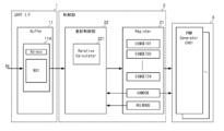
- FIG. 4 is a diagram showing a configuration example regarding updating of dimming settings in a semiconductor device.
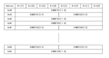
- FIG. 5 is a diagram showing a register map in the high resolution mode.
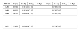
- FIG. 6 is a diagram showing the correspondence between addresses transmitted by the reception data RX and data corresponding to the addresses.
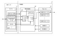
- FIG. 7 is a block diagram showing an example of updating the dimming setting data in the high resolution mode and the relative mode.
- FIG. 1 is a diagram illustrating a configuration of a communication system according to an exemplary embodiment of the present disclosure.
- FIG. 2 is a diagram showing a configuration of a semiconductor device according to an exemplary embodiment of the present disclosure.
- FIG. 3 is a diagram showing the
- FIG. 8A is a diagram showing an example of data transmitted by the reception data RX in the high resolution mode and the absolute mode.
- FIG. 8B is a diagram showing an example of data transmitted by the reception data RX in the high resolution mode and the absolute mode.
- FIG. 8C is a diagram showing an example of data transmitted by the reception data RX in the high resolution mode and the absolute mode.
- FIG. 9 is a block diagram showing an example of updating dimming setting data in the high resolution mode and the absolute mode.
- FIG. 10 is a diagram showing an example of a correspondence relationship between the range of the on-duty when gradation dimming is performed and the steps by which the on-duty is changed.
- FIG. 11 is a diagram showing a register map in the low resolution mode.
- FIG. 12 is a block diagram showing an example of updating dimming setting data in the low resolution mode and the absolute mode.
- FIG. 13 is a diagram showing a register map relating to the group setting function.
- FIG. 14 is a configuration diagram showing an example of updating dimming setting data using the group setting function.
- Communication System 1 is a diagram showing a configuration of a communication system 501 according to an exemplary embodiment of the present disclosure.
- the communication system 501 includes an MCU (Micro Controller Unit) 20, a CAN (Controller Area Network) transceiver 30, a CAN transceiver 40, and a plurality of semiconductor devices 10. Note that the communication system 501 is used, for example, in a vehicle.
- MCU Micro Controller Unit
- CAN Controller Area Network
- UART Universal Asynchronous Receiver/Transmitter
- CAN is a serial communication protocol standardized in international standards such as ISO 11898.
- the CAN transceiver 30 has a TXD (transmit data input) terminal 30A and a RXD (receive data output) terminal 30B.
- the CAN transceiver 30 outputs data input to the TXD terminal 30A to the CAN bus 35, and outputs data input from the CAN bus 35 from the RXD terminal 30B.
- the CAN transceiver 40 has an RXD terminal 40A and a TXD terminal 40B.
- the CAN transceiver 40 outputs data input to the TXD terminal 40B to the CAN bus 35, and outputs data input from the CAN bus 35 from the RXD terminal 40A.
- the semiconductor device 10 is an IC (integrated circuit) in which circuits with specific functions are integrated, and is configured as, for example, an LED (light emitting diode) driver IC. All of the multiple semiconductor devices 10 may be LED driver ICs, or some of the semiconductor devices may be LED driver ICs. Details of the semiconductor device 10 as an LED driver IC will be described later.
- the semiconductor device 10 has an RX (received data input) terminal 10A and a TX (transmitted data output) terminal 10B.
- the RX terminals 10A of the multiple semiconductor devices 10 are commonly connected to an RXD terminal 40A.
- the TX terminals 10B of the multiple semiconductor devices 10 are commonly connected to a TXD terminal 40B.
- the received data RX output from the RXD terminal 40A is input to the RX terminal 10A of each of the multiple semiconductor devices 10.
- the device address of one of the multiple semiconductor devices 10 is specified in the received data RX.
- the transmitted data TX output from the TX terminal 10B of each of the multiple semiconductor devices 10 is input to the TXD terminal 40B.
- FIG. 2 is a diagram showing a configuration of a semiconductor device 10 according to an exemplary embodiment of the present disclosure.
- the semiconductor device 10 shown in Fig. 2 is configured as an LED driver IC that drives an LED 6.
- An LED is an example of a light-emitting element.
- an LED driver is an example of a light-emitting element driving device.
- LEDs 6 are provided in multiple channels.
- the LEDs 6 have 24 channels as an example.
- the LEDs 6 may have multiple channels other than 24 channels, or may have a single channel.
- the LEDs 6 in each channel are each configured with LED elements connected in series. However, the LEDs 6 in each channel may be configured with LED elements connected in series/parallel, or may be configured with a single LED element.
- the semiconductor device 10 includes an integrated UART interface 1, a control unit 2, a PWM generating unit 3, and a current driver 4.
- the semiconductor device 10 also includes an RX terminal 10A, a TX terminal 10B, and a cathode terminal 10C as external terminals for establishing electrical connection with the outside.
- receive data RX input from the outside to RX terminal 10A is input to UART interface 1. Also, transmit data TX output from UART interface 1 is output to the outside from TX terminal 10B as mentioned above.
- the control unit 2 has a register 21.
- the control unit 2 updates the data in the register 21 based on the write data included in the received data RX.
- the control unit 2 reads data from the register 21. Details of the RX data will be described later.
- the PWM generating unit 3 is provided corresponding to each channel of the LED 6. Therefore, if the LED 6 has 24 channels, a PWM generating unit 3 is provided for each of the channels CH01 to CH24. Note that channel CHn corresponds to the nth channel.
- the dimming setting data for each channel is stored in the register 21.
- the PWM generating unit 3 for each channel generates a PWM signal with an on-duty based on the dimming setting data for each channel. In other words, the dimming setting data for each channel represents the on-duty for PWM dimming for each channel.
- a PWM signal is a pulse signal consisting of a high level and a low level.
- the period when the PWM signal is at the first level is the on period
- the period when the PWM signal is at the second level is the off period.
- the current driver 4 is provided for each channel of the LED 6. Therefore, if the LED 6 has 24 channels, a current driver 4 is provided for each of the channels CH01 to CH24.
- the current driver 4 for each channel is connected to the cathode of the LED 6 for each channel via the cathode terminal 10C.
- the anodes of the LED 6 for each channel are commonly connected to the application terminal of the power supply voltage Vcc.
- Each PWM signal generated by the PWM generation unit 3 of each channel is used to control the on/off state of the current driver 4 of each channel. Specifically, during the on period of the PWM signal, the current driver 4 is in the on state, and during the off period of the PWM signal, the current driver 4 is in the off state. When the current driver 4 is in the on state, a constant current flows through the LED 6, causing the LED 6 to emit light. When the current driver 4 is in the off state, no constant current flows through the LED 6, causing the LED 6 to turn off.
- the on-duty of PWM dimming is the percentage of the on-period in one cycle. The higher the on-duty, the brighter the LED 6.
- the dimming setting data for each channel can be updated based on the received data RX via UART communication, and the LEDs 6 for each channel can be PWM dimmed based on the on-duty set for each channel.
- the dimming setting data for all 24 channels can be updated by a single communication of received data RX, or the dimming setting data for only some of the channels (single or multiple channels) can be updated.
- Structure of received data 3 is a diagram showing the data structure of the received data RX.
- communication is performed in data units called frames.
- a frame is made up of bit data from a start bit to a stop bit. The start bit is at a low level, and the stop bit is at a high level.
- a predetermined number of bits of bit data are placed between the start bit and the stop bit. In the following, the predetermined number of bits is assumed to be 8 bits as an example. In this case, a frame is made up of 10 bits of bit data.
- the received data RX includes, from the beginning, a synchronization frame SYNC, a device frame Device, a data number frame NumofData, an address frame Address, data frames Data1 to DataN (N is an integer equal to or greater than 1), a CRC (Cyclic Redundancy Check) lower frame CRC16L, and a CRC upper frame CRC16H.
- a synchronization frame SYNC a device frame Device
- a data number frame NumofData an address frame Address
- data frames Data1 to DataN N is an integer equal to or greater than 1
- CRC Cyclic Redundancy Check
- the synchronization frame SYNC is bit data for setting the baud rate in the semiconductor device 10.
- the device frame Device includes a device address and a Read/Write bit.
- the device address is bit data that indicates the address of the target device (semiconductor device 10).
- the Read/Write bit is bit data that indicates a read or write.
- the data number frame NumofData is bit data that indicates the number of frames (i.e., N) in the data frames Data1 to DataN.
- the address frame Address is bit data that indicates the address for accessing the register 21.
- the data frames Data1 to DataN are bit data that indicate data for updating the data in the register 21. Note that if the Read/Write bit in the device frame Device indicates a read, the data frames Data1 to DataN are not included in the received data RX.
- the CRC lower frame CRC16L and the CRC upper frame CRC16H are bit data that indicate error detection codes added to the data frames Data1 to DataN.
- Fig. 4 is a diagram showing an example of a configuration for updating the dimming setting in the semiconductor device 10.
- the UART interface 1 has a buffer 11.
- receive data 11A is stored in the buffer 11.
- receive data 11A includes address data Address and write data WDT.
- the write data WDT is data transmitted by the data frame DataN (FIG. 3).
- the control unit 2 has an update control unit 22 together with a register 21.
- the update control unit 22 updates the dimming setting data DIMSET01 to DIMSET24 in the register 21 based on the received data 11A.
- the update control unit 22 has a relative calculation unit 221.
- the relative calculation unit 221 is used in the case of a relative update of the dimming setting data, which will be described later.
- the dimming setting data DIMSET01 to DIMSET24 is stored in register 21.
- the dimming setting data DIMSETn is the dimming setting for channel CHn and indicates the on-duty of channel CHn.
- the on-duty is a value between 0 and 100%.
- Resolution setting data HAMODE and relative mode setting data RELMODE are stored in register 21.
- the resolution setting data HAMODE is 1-bit data, and indicates the setting of high resolution mode or low resolution mode.
- the high resolution mode is a mode in which the dimming setting data DIMSETn is updated as a first predetermined number of bits (e.g., 12 bits), and the on-duty can be adjusted with a resolution of the first predetermined number of bits. If the first predetermined number of bits is, for example, 12 bits, the on-duty can be adjusted in steps of about 0.02%.
- the low resolution mode is a mode in which the dimming setting data DIMSETn is updated as a second predetermined number of bits (e.g., 8 bits) lower than the first predetermined number of bits, and the on-duty can be adjusted with a resolution of the second predetermined number of bits. If the second predetermined number of bits is, for example, 8 bits, the on-duty can be adjusted in steps of about 0.4%.
- the relative mode setting data RELMODE is 1-bit data that indicates the setting of relative or absolute mode.
- Relative mode is a mode in which the dimming setting data DIMSETn is updated based on the relative change from the current value.
- Absolute mode is a mode in which the dimming setting data DIMSETn is updated with an absolute value.
- the first predetermined number of bits is assumed to be 12 bits, as an example.
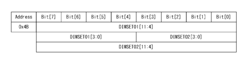
- FIG. 5 is a diagram showing the storage of dimming setting data DIMSETn in register 21 in high resolution mode. That is, FIG. 5 shows a register map. FIG. 5 shows the correspondence between addresses in register 21 and the dimming setting data DIMSETn stored in those addresses. As shown in FIG. 5, 8 bits of data can be stored in one address. The number of bits that can be stored in one address in register 21 is the second predetermined number of bits (the number of low resolution bits).
- Address 0x4B stores the upper 8 bits of DIMSET01.
- Address 0x4C stores the lower 4 bits of DIMSET01 in the upper part, and the lower 4 bits of DIMSET02 in the lower part.
- Address 0x4D stores the upper 8 bits of DIMSET02. Similar to this storage pattern of dimming setting data at addresses 0x4B to 0x4D, DIMSET03 to DIMSET24 are also stored at addresses 0x4E and onwards. In this way, 12 bits of DIMSET01 to DIMSET24 can be stored in each of the consecutive addresses from 0x4B to 0x6E.
- Figure 6 is a diagram showing the correspondence between the address transmitted by the received data RX in this case and the data corresponding to that address.
- the address shown in Figure 6 is transmitted by the address frame Address ( Figure 3).
- the 8-bit data (Bit [7:0]) shown in Figure 6 is transmitted by the data frame DataN ( Figure 3).
- the 8-bit data includes polarity data CHnSG, gain data CHnGAIN, and relative value data DUTYn.
- the polarity data CHnSG, gain data CHnGAIN, and relative value data DUTYn are data corresponding to channel CHn.
- the relative value data DUTYn is 5-bit data and indicates the relative change value.
- the relative value data DUTYn can take a value from 0 to 31.
- the dimming setting data DIMSETn of the channel CHn is updated as follows based on the polarity data CHnSG, the gain data CHnGAIN, and the relative value data DUTYn.
- DIMSETn DIMSETn ⁇ DUTYn ⁇ CHnGAIN Note that DIMSETn on the right side indicates the current value, and DIMSETn on the left side indicates the updated value.
- ⁇ indicates + (increase) or ⁇ (decrease) according to the polarity data CHnSG.
- DIMSETn DIMSETn - 5 x 2.
- the 8-bit data corresponding to the address shown in Figure 6 is the data transmitted in the first data frame Data1 when that address is transmitted in the address frame Address. It is possible to transmit only one channel's worth of the first data frame Data1, but when transmitting multiple channels, data for consecutive channels is transmitted in multiple data frames starting from the first data frame Data1. For example, when transmitting data for 24 channels, the address transmitted in the address frame Address is set to 0x4B, and 24 channels' worth of data (CH01SG to CH24SG, CH01GAIN to CH24GAIN, DUTY01 to DUTY24) is transmitted in 24 data frames Data1 to Data24.
- the example in Figure 7 shows a case where the address 0x4B is transmitted by the address frame Address.
- Received data RX is input to the UART interface 1, and received data 11A is stored in the buffer 11.
- the received data 11A includes write data WDT along with an address 0x4B.
- the write data WDT includes polarity data CH01SG, gain data CH01GAIN, and relative value data DUTY01 corresponding to channel CH01. In this case, the following calculation is performed in the relative calculation unit 221.
- DIMSET01 DIMSET01 ⁇ DUTY01 ⁇ CH01GAIN
- the value of the dimming setting data DIMSET01 in register 21 is updated based on the value of the dimming setting data DIMSET01 for channel CH01 calculated as above.
- dimming setting data DIMSETn for channels CH02 and onward which are not shown in Figure 7, is updated in the same manner as above.
- the following transmission is performed by the received data RX.
- the address corresponding to the first channel for which it is desired to update the dimming setting data is specified in the address frame Address.
- dimming setting data DIMSETn corresponding to consecutive addresses from the specified address in the register map is transmitted by the data frame DataN for the required number of channels.
- Figure 8A shows the data transmitted by the receive data RX when the only channel desired to be updated is channel CH01.
- 0x4B is specified in the address frame Address
- the upper bits of DIMSET01 are transmitted by the data frame Data1
- the lower bits of DIMSET01 are transmitted by the data frame Data2.
- the lower bits of DIMSET02 for channel CH02 are set as dummy data.
- FIG. 8B shows data transmitted by receive data RX when the channels desired to be updated are channels CH01 and CH02.
- 0x4B is specified in the address frame Address
- the upper bits of DIMSET01 are transmitted by data frame Data1
- the lower bits of DIMSET01 and the lower bits of DIMSET02 are transmitted by data frame Data2
- the upper bits of DIMSET02 are transmitted by data frame Data3.
- Figure 8C shows data transmitted by receive data RX when the only channel desired to be updated is channel CH02.
- 0x4C is specified in the address frame Address
- the lower bits of DIMSET02 are transmitted by data frame Data1
- the upper bits of DIMSET02 are transmitted by data frame Data2.
- the lower bits of DIMSET01 for channel CH01 are set as dummy data.
- the dimming setting data DIMSETn in register 21 is updated by the dimming setting data DIMSETn transmitted as described above. However, the data in register 21 is not updated by dummy data.
- the example in Figure 9 shows a case where only the dimming setting data DIMSET01 of channel CH01 is updated.
- Received data RX is input to the UART interface 1, and received data 11A is stored in the buffer 11.
- Received data 11A includes write data WDT along with address 0x4B.
- the write data WDT stores the upper and lower bits of DIMSET01 and the lower bits of DIMSET02 ( Figure 8A).
- the update control unit 22 updates DIMSET01 in the register 21 based on address 0x4B and the upper and lower bits of DIMSET01.
- FIG. 10 is a diagram showing an example of the correspondence between the on-duty range when performing gradation dimming and the step by which the on-duty is changed.
- the higher the duty the larger the step.
- the on-duty is increased from the current value to the target value in specified steps.
- the minimum step can be made small.
- the necessary steps are small, so dimming is possible by updating the dimming setting data in relative mode. Note that if it is necessary to change the on-duty significantly, absolute mode can be used.
- the multiple semiconductor devices 10 are assumed to be LED driver ICs. In this case, when updating the dimming setting data in each of the multiple semiconductor devices 10, it is necessary to transmit the received data RX to each of the multiple semiconductor devices 10 in sequence by serial communication, and it is effective to reduce the amount of communication in one transmission.
- FIG. 11 is a diagram (register map) showing the storage of dimming setting data DIMSETn in register 21 in low resolution mode.
- FIG. 11 shows the correspondence between addresses in register 21 and the dimming setting data DIMSETn stored at those addresses.
- the following transmission is performed by the received data RX.
- the address corresponding to the first channel for which it is desired to update the dimming setting data is specified in the address frame Address.
- dimming setting data DIMSETn corresponding to consecutive addresses from the specified address in the register map is transmitted by the data frame DataN for the required number of channels.
- DIMSET01 to DIMSET24 are transmitted using data frames Data1 to Data24.
- receive data RX is input to the UART interface 1, and receive data 11A is stored in the buffer 11.
- the receive data 11A includes write data WDT along with address 0x4B.
- the write data WDT includes DIMSET01, DIMSET02, etc.
- the update control unit 22 updates DIMSET01, DIMSET02, etc. in the register 21 based on the address 0x4B and DIMSET01, DIMSET02, etc.
- the dimming setting data DIMSETn can be updated with an address incremented from the specified address. In other words, when updating dimming setting data DIMSETn for multiple channels, it is possible to update by sending received data RX once, reducing the amount of communication.
- the semiconductor device 10 of the present embodiment may have a group setting function as described below.
- FIG. 13 is a diagram showing a register map in register 21 related to the group setting function.
- group setting data CHnDTYGRP is stored in each of the consecutive addresses from address 0x32 to 0x37.
- CH04DTYGRP to CH01DTYGRP are stored in address 0x32 from the most significant bit
- CH08DTYGRP to CH05DTYGRP are stored in address 0x33 from the most significant bit, and so on up to CH24DTYGRP.
- duty setting value data DTYGRPm is stored in each of the consecutive addresses from address 0x38 to 0x3C.
- the duty setting value data DTYGRPm is 12-bit data, and indicates the on-duty value set for the mth group.
- the upper 8 bits of DTYGRP1 are stored at address 0x38
- the lower 4 bits of DTYGRP2 and the lower 4 bits of DTYGRP1 are stored at address 0x39
- the upper 8 bits of DTYGRP2 are stored at address 0x3A
- the upper 8 bits of DTYGRP3 are stored at address 0x3B
- the lower 4 bits of DTYGRP3 are stored at address 0x3C.
- all channel update mode setting data GRPALL (1 bit) is stored at address 0x3C.
- address 0x32 is specified in the address frame Address, and in addition to the group setting data CH01DTYGRP to CH24DTYGRP, the duty setting value data DTYGRPm for the required number of groups is sent in the data frame DataN.
- the group setting data CH01DTYGRP to CH24DTYGRP and the duty setting value data DTYGRPm in register 21 are updated based on the data transmitted by the receive data RX. Then, the dimming setting data DIMSETn of the channels CHn grouped by the group setting data CH01DTYGRP to CH24DTYGRP is updated based on the duty setting value data DTYGRPm corresponding to each group.
- FIG. 14 is a configuration diagram (corresponding to FIG. 4) showing an example of updating dimming setting data DIMSETn using the group setting function.
- receive data RX is input to the UART interface 1, and receive data 11A is stored in the buffer 11.
- the receive data 11A includes write data WDT along with an address 0x32.
- the write data WDT includes group setting data CH01DTYGRP to CH24DTYGRP and duty setting value data DTYGRP1, 2. That is, in the example of FIG. 14, the number of groups to be divided is set to 2.
- the update control unit 22 updates the group setting data CH01DTYGRP to CH24DTYGRP in the register 21 based on the group setting data CH01DTYGRP to CH24DTYGRP, and updates the duty setting value data DTYGRP1, 2 in the register 12 based on the duty setting value data DTYGRP1, 2.
- dimming setting data DIMSET01-08 is updated by duty setting value data DTYGRP1
- dimming setting data DIMSET09-24 is updated by duty setting value data DTYGRP2.
- the dimming setting data is updated by update control unit 22.
- the group setting function is enabled and the all-channel update mode is disabled.
- GRPALL is, for example, 1
- the group setting function is disabled and the all-channel update mode is enabled.
- the dimming setting data DIMSETn for all channels (24 channels) is updated to the same value based on, for example, DTYGRP3.
- serial communication is not limited to UART communication, but may be I 2 C communication or the like.
- the semiconductor device (10) is An interface unit (1) configured to receive write data (WDT) transmitted from an external device via serial communication; an update control unit (22) having a relative calculation unit (221) configured to perform calculations based on the write data; A register (21) configured to store duty setting data (DIMSETn) indicating a duty value of a PWM; Equipped with The write data is Polarity data (CHnSG) representing a decrease or increase; Gain data (CHnGAIN) representing a gain value; Relative value data (DUTYn) representing a relative change value; Including, the relative calculation unit calculates a calculation result by subtracting or adding a value obtained by multiplying the relative change value by the gain value to a current value of the duty setting data according to the polarity data; The update control section is configured to update the duty setting data based on the calculation result (first configuration).
- WDT write data
- a register (21) configured to store duty setting data (DIMSETn) indicating a duty value of a PWM
- DIMSETn duty setting data
- This configuration allows the PWM duty value to be updated relatively, reducing the amount of data written. This solves the problem of reducing the amount of serial communication traffic when setting PWM control.
- the gain value may be set to 1 by the gain data (second configuration).
- the total number of bits (e.g., 8 bits) of the polarity data, gain data, and relative value data may be smaller than the first predetermined number of bits (e.g., 12 bits) of the duty setting data (third configuration).
- a relative mode in which the update control unit updates the duty setting data based on the calculation result an absolute mode in which the update control unit updates the duty setting data stored in the register by the duty setting data of the first predetermined number of bits included in the write data transmitted by the serial communication; (fourth configuration).
- a high resolution mode in which the duty setting data stored in the register has the first predetermined number of bits for example, 12 bits
- a low resolution mode in which the duty setting data stored in the register has a second predetermined number of bits (e.g., 8 bits) which is smaller than the first predetermined number of bits (fifth configuration).
- the number of bits of data that can be stored in one address in the register is the second predetermined number of bits
- the register In the high resolution mode, in the register, upper bits of the duty setting data of a first channel are stored in a first address (e.g., 0x4B), lower bits of the duty setting data of the first channel and lower bits of the duty setting data of a second channel are stored in a second address (e.g., 0x4C) obtained by incrementing the first address, and upper bits of the duty setting data of the second channel are stored in a third address (e.g., 0x4D) obtained by incrementing the second address.
- the register In the low resolution mode, the register may be configured so that the duty setting data for each channel is stored for each successive address (sixth configuration, FIG. 5 and FIG. 11).
- the duty setting data for a plurality of channels is stored in the register,
- the polarity data, the gain data, and the relative value data may correspond to the multiple channels (seventh configuration).
- any of the first to seventh configurations above it may be possible to configure it so that PWM dimming can be performed based on the duty setting data (eighth configuration).
- the higher the on-duty of the PWM dimming, the larger the step for changing the on-duty, and gradation dimming in which the on-duty is increased according to the step may be possible (ninth configuration).
- the duty setting data for a plurality of channels is stored in the register
- the update control unit may be configured to update the duty setting data based on the group setting data and the duty setting value data (tenth configuration).
- a mode in which the duty setting data corresponding to all of the plurality of channels is updated based on the duty setting value data corresponding to a predetermined group may be switchable (eleventh configuration).
- the serial communication may be UART communication (configuration 12).
- a communication system (501) is configured to include a semiconductor device (10) having any one of the first to twelfth configurations described above, and a transmitting device (40) configured to transmit the write data (thirteenth configuration).
- the input terminal (10A) provided in each of the multiple semiconductor devices and configured to input the write data may be commonly connected to the same output terminal (40A) provided in the transmitting device (fourteenth configuration).
- This disclosure can be used, for example, in vehicle-mounted communication systems.
Landscapes
- Circuit Arrangement For Electric Light Sources In General (AREA)
Abstract
シリアル通信により送信された書き込みデータ(WDT)は、減少または増加を表す極性データ(CHnSG)と、ゲイン値を表すゲインデータ(CHnGAIN)と、相対変化値を表す相対値データ(DUTYn)と、を含み、相対計算部(221)は、前記相対変化値に前記ゲイン値を乗算して得られる値を現状のデューティ設定データ(DIMSETn)の値に対して、前記極性データに応じて減算または加算して計算結果を算出し、更新制御部(22)は、前記計算結果によって前記デューティ設定データを更新する。
Description
本開示は、半導体装置、および通信システムに関する。
シリアル通信機能を備えた半導体装置が種々のアプリケーションで利用されている。
なお、シリアル通信に関する回路技術の一例は、特許文献1に開示されている。
[概要]
ここで、半導体装置は、例えば発光素子を駆動する装置として、PWM(Pulse Width Modulation)調光を行う機能を有する場合がある。このようなPWM調光などのPWM制御を行う場合に、デューティをシリアル通信により設定する場合がある。この場合、半導体装置へシリアル通信によって送信するデータ量をなるべく低減することが要望される。
ここで、半導体装置は、例えば発光素子を駆動する装置として、PWM(Pulse Width Modulation)調光を行う機能を有する場合がある。このようなPWM調光などのPWM制御を行う場合に、デューティをシリアル通信により設定する場合がある。この場合、半導体装置へシリアル通信によって送信するデータ量をなるべく低減することが要望される。
本開示は、PWM制御の設定時におけるシリアル通信の通信量を低減することが可能となる半導体装置を提供することを目的とする。
例えば、本開示の一態様に係る半導体装置は、
シリアル通信により送信された書き込みデータを外部から受信するように構成されるインタフェース部と、
前記書き込みデータに基づいて計算を行うように構成される相対計算部を有する更新制御部と、
PWMのデューティ値を示すデューティ設定データが格納されるように構成されるレジスタと、
を備え、
前記書き込みデータは、
減少または増加を表す極性データと、
ゲイン値を表すゲインデータと、
相対変化値を表す相対値データと、
を含み、
前記相対計算部は、前記相対変化値に前記ゲイン値を乗算して得られる値を現状の前記デューティ設定データの値に対して、前記極性データに応じて減算または加算して計算結果を算出し、
前記更新制御部は、前記計算結果によって前記デューティ設定データを更新する構成としている。
シリアル通信により送信された書き込みデータを外部から受信するように構成されるインタフェース部と、
前記書き込みデータに基づいて計算を行うように構成される相対計算部を有する更新制御部と、
PWMのデューティ値を示すデューティ設定データが格納されるように構成されるレジスタと、
を備え、
前記書き込みデータは、
減少または増加を表す極性データと、
ゲイン値を表すゲインデータと、
相対変化値を表す相対値データと、
を含み、
前記相対計算部は、前記相対変化値に前記ゲイン値を乗算して得られる値を現状の前記デューティ設定データの値に対して、前記極性データに応じて減算または加算して計算結果を算出し、
前記更新制御部は、前記計算結果によって前記デューティ設定データを更新する構成としている。
[詳細な説明]
以下、本開示の例示的な実施形態について、図面を参照して説明する。
以下、本開示の例示的な実施形態について、図面を参照して説明する。
<1.通信システム>
図1は、本開示の例示的な実施形態に係る通信システム501の構成を示す図である。通信システム501は、MCU(Micro Controller Unit)20と、CAN(Controller Area Network)トランシーバ30と、CANトランシーバ40と、複数の半導体装置10と、を備える。なお、通信システム501の用途は、一例として車載用である。
図1は、本開示の例示的な実施形態に係る通信システム501の構成を示す図である。通信システム501は、MCU(Micro Controller Unit)20と、CAN(Controller Area Network)トランシーバ30と、CANトランシーバ40と、複数の半導体装置10と、を備える。なお、通信システム501の用途は、一例として車載用である。
MCU20とCANトランシーバ30との間では、UART(Universal Asynchronous Receiver/Transmitter)による通信が行われる。UARTは、2つのデバイス間でシリアルデータを交換するためのプロトコルである。UARTでは、送信側と受信側の間で2本のラインにより双方向の通信が行われる。
CANトランシーバ30,40との間では、CANバス35による通信が行われる。CANは、国際標準規格のISO11898等で標準化されているシリアル通信プロトコルである。
CANトランシーバ30は、TXD(送信データ入力)端子30AとRXD(受信データ出力)端子30Bを有する。CANトランシーバ30は、TXD端子30Aに入力されたデータをCANバス35へ出力し、CANバス35から入力されたデータをRXD端子30Bから出力する。
CANトランシーバ40は、RXD端子40AとTXD端子40Bを有する。CANトランシーバ40は、TXD端子40Bに入力されたデータをCANバス35へ出力し、CANバス35から入力されたデータをRXD端子40Aから出力する。
半導体装置10は、所定機能の回路が集積化されたIC(集積回路)であり、例えばLED(発光ダイオード)ドライバICとして構成される。複数の半導体装置10は、すべての半導体装置がLEDドライバICであってもよいし、一部の半導体装置がLEDドライバICであってもよい。なお、LEDドライバICとしての半導体装置10の詳細については、後述する。
半導体装置10は、RX(受信データ入力)端子10AとTX(送信データ出力)端子10Bを有する。複数の半導体装置10のそれぞれのRX端子10Aは、RXD端子40Aに共通接続される。複数の半導体装置10のそれぞれのTX端子10Bは、TXD端子40Bに共通接続される。
RXD端子40Aから出力される受信データRXは、複数の半導体装置10のそれぞれのRX端子10Aに入力される。受信データRXには、複数の半導体装置10のうちいずれかのデバイスアドレスが指定されている。また、複数の半導体装置10のそれぞれのTX端子10Bから出力される送信データTXは、TXD端子40Bに入力される。
<2.半導体装置の構成>
図2は、本開示の例示的な実施形態に係る半導体装置10の構成を示す図である。図2に示す半導体装置10は、LED6を駆動するLEDドライバICとして構成される。LEDは、発光素子の一例である。すなわち、LEDドライバは、発光素子駆動装置の一例である。
図2は、本開示の例示的な実施形態に係る半導体装置10の構成を示す図である。図2に示す半導体装置10は、LED6を駆動するLEDドライバICとして構成される。LEDは、発光素子の一例である。すなわち、LEDドライバは、発光素子駆動装置の一例である。
LED6は、複数チャンネル設けられる。以下、LED6のチャンネルを一例として24チャンネルであるとする。なお、LED6のチャンネルは、24チャンネル以外の複数チャンネルであってもよいし、単数のチャンネルであってもよい。各チャンネルのLED6は、それぞれLED素子が直列に接続されて構成される。ただし、各チャンネルのLED6は、LED素子が直並列に接続されて構成されてもよいし、単数のLED素子から構成されてもよい。
半導体装置10は、UARTインタフェース1と、制御部2と、PWM生成部3と、電流ドライバ4と、を集積化して備える。また、半導体装置10は、外部との電気的接続を確立するための外部端子として、RX端子10A、TX端子10B、およびカソード端子10Cを備える。
先述したようにRX端子10Aに外部から入力された受信データRXは、UARTインタフェース1に入力される。また、UARTインタフェース1から出力された送信データTXは、先述したようにTX端子10Bから外部へ出力される。
制御部2は、レジスタ21を有する。UARTインタフェース1に入力された受信データRXがライト(書き込み)を示す場合、制御部2はレジスタ21を受信データRXに含まれる書き込みデータに基づいてレジスタ21のデータを更新(アップデート)する。一方、UARTインタフェース1に入力された受信データRXがリード(読み出し)を示す場合、制御部2はレジスタ21からデータを読み出す。なお、RXデータの詳細については後述する。
PWM生成部3は、LED6の各チャンネルに対応して設けられる。従って、LED6が24チャンネルであれば、PWM生成部3はチャンネルCH01からチャンネルCH24のそれぞれについて設けられる。なお、チャンネルCHnは、第nチャンネルに相当する。レジスタ21には、各チャンネルの調光設定データが格納される。各チャンネルのPWM生成部3は、それぞれ、各チャンネルの調光設定データに基づいたオンデューティのPWM信号を生成する。すなわち、各チャンネルの調光設定データは、各チャンネルのPWM調光用のオンデューティを表す。
PWM信号は、ハイレベルとローレベルからなるパルス信号である。1周期(PWM周期)において、PWM信号の第1レベル(例えばハイレベル)の期間がオン期間であり、PWM信号の第2レベル(例えばローレベル)の期間がオフ期間である。
電流ドライバ4は、LED6の各チャンネルに対応して設けられる。従って、LED6が24チャンネルであれば、電流ドライバ4はチャンネルCH01からチャンネルCH24のそれぞれについて設けられる。各チャンネルの電流ドライバ4は、それぞれ、各カソード端子10Cを介して各チャンネルのLED6のカソードに接続される。なお、各チャンネルのLED6のアノードは、電源電圧Vccの印加端に共通接続される。
各チャンネルのPWM生成部3により生成された各PWM信号は、それぞれ、各チャンネルの電流ドライバ4のオンオフ制御に用いられる。具体的には、PWM信号のオン期間では、電流ドライバ4がオン状態とされ、PWM信号のオフ期間では、電流ドライバ4がオフ状態とされる。電流ドライバ4がオン状態の場合、LED6に定電流が流れ、LED6が発光する。電流ドライバ4がオフ状態の場合、LED6に定電流が流れず、LED6が消灯する。PWM調光のオンデューティは、オン期間の1周期における割合である。オンデューティが高いほど、LED6は明るくなる。
このような構成により、UART通信による受信データRXに基づいて各チャンネルの調光設定データを更新し、各チャンネルに設定された各オンデューティに基づいて各チャンネルのLED6をPWM調光することができる。なお、後述するように、本実施形態では、1回の受信データRXの通信により、24チャンネルすべてのチャンネルの調光設定データを更新することもできるし、一部のチャンネル(単数または複数チャンネル)のみの調光設定データを更新することもできる。
<3.受信データの構成>
図3は、受信データRXのデータ構成を示す図である。UARTでは、フレームと呼ばれるデータ単位により通信が行われる。フレームは、スタートビットからストップビットまでのビットデータで構成される。スタートビットはローレベル、ストップビットはハイレベルとなる。スタートビットとストップビットの間には、所定ビット数のビットデータが配置される。以下では、一例として所定ビット数が8ビットであるとする。この場合、フレームは、10ビットのビットデータから構成される。
図3は、受信データRXのデータ構成を示す図である。UARTでは、フレームと呼ばれるデータ単位により通信が行われる。フレームは、スタートビットからストップビットまでのビットデータで構成される。スタートビットはローレベル、ストップビットはハイレベルとなる。スタートビットとストップビットの間には、所定ビット数のビットデータが配置される。以下では、一例として所定ビット数が8ビットであるとする。この場合、フレームは、10ビットのビットデータから構成される。
図3に示すように、受信データRXは、同期フレームSYNC、デバイスフレームDevice、データ数フレームNumofData、アドレスフレームAddress、データフレームData1~DataN(Nは1以上の整数)、CRC(Cyclic Redundancy Check)下位フレームCRC16L、およびCRC上位フレームCRC16Hを先頭から順に有する。
同期フレームSYNCは、半導体装置10にボーレートを設定するためのビットデータである。
デバイスフレームDeviceは、デバイスアドレスおよびRead/Writeビットなどを含む。デバイスアドレスは、対象デバイス(半導体装置10)のアドレスを示すビットデータである。Read/Writeビットは、リードあるいはライトを示すビットデータである。
データ数フレームNumofDataは、データフレームData1~DataNのフレーム数(すなわちN)を示すビットデータである。
アドレスフレームAddressは、レジスタ21へのアクセスのためのアドレスを示すビットデータである。
データフレームData1~DataNは、レジスタ21のデータ更新用のデータを示すビットデータである。なお、デバイスフレームDeviceにおいてRead/Writeビットがリードを示す場合は、データフレームData1~DataNは受信データRXに含められない。
CRC下位フレームCRC16LおよびCRC上位フレームCRC16Hは、データフレームData1~DataNに対して付加される誤り検出符号を示すビットデータである。
<4.調光設定の更新>
次に、レジスタ21における調光設定データの更新方法について説明する。図4は、半導体装置10における調光設定の更新に関する構成例を示す図である。
次に、レジスタ21における調光設定データの更新方法について説明する。図4は、半導体装置10における調光設定の更新に関する構成例を示す図である。
図4に示すように、UARTインタフェース1は、バッファ11を有する。受信データRXがUARTインタフェース11に入力されると、受信データ11Aがバッファ11に格納される。受信データ11Aは、アドレスデータAddressと書き込みデータWDTを含む。書き込みデータWDTは、データフレームDataN(図3)により送信されるデータである。
制御部2は、レジスタ21とともに更新制御部22を有する。更新制御部22は、受信データ11Aに基づいてレジスタ21における調光設定データDIMSET01~DIMSET24を更新する。更新制御部22は、相対計算部221を有する。相対計算部221は、後述する調光設定データの相対的更新の場合に用いられる。
レジスタ21には、調光設定データDIMSET01~DIMSET24が格納される。調光設定データDIMSETnは、チャンネルCHnの調光設定であり、チャンネルCHnのオンデューティを示す。オンデューティは、0~100%の値である。
レジスタ21には、分解能設定データHAMODEと相対モード設定データRELMODEが格納される。
分解能設定データHAMODEは、1ビットのデータであり、高分解能モードあるいは低分解能モードの設定を示す。高分解能モードは、調光設定データDIMSETnを第1所定ビット数(例えば12ビット)として更新するモードであり、オンデューティを第1所定ビット数の分解能で調整可能である。第1所定ビット数が例えば12ビットの場合は、オンデューティを約0.02%のステップで調整可能である。低分解能モードは、調光設定データDIMSETnを第1所定ビット数よりも低い第2所定ビット数(例えば8ビット)として更新するモードであり、オンデューティを第2所定ビット数の分解能で調整可能である。第2所定ビット数が例えば8ビットの場合は、オンデューティを約0.4%のステップで調整可能である。
相対モード設定データRELMODEは、1ビットのデータであり、相対モードあるいは絶対モードの設定を示す。相対モードは、調光設定データDIMSETnを現状の値からの相対的な変化により更新するモードである。絶対モードは、調光設定データDIMSETnを絶対値で更新するモードである。
<<高分解能モードの場合>>
ここでは、分解能モードが高分解能モードに設定された場合(HAMODE=1)の調光設定データの更新方法について説明する。ここで、上記第1所定ビット数は一例として12ビットであるとする。
ここでは、分解能モードが高分解能モードに設定された場合(HAMODE=1)の調光設定データの更新方法について説明する。ここで、上記第1所定ビット数は一例として12ビットであるとする。
図5は、高分解能モードの場合のレジスタ21における調光設定データDIMSETnの格納を示す図である。すなわち、図5は、レジスタマップを示す。図5では、レジスタ21におけるアドレスと、当該アドレスに格納される調光設定データDIMSETnの対応関係を示す。図5に示すように、1つのアドレスには8ビットのデータが格納可能である。レジスタ21において1つのアドレスに格納可能なビット数は、上記第2所定ビット数(低分解能のビット数)である。
なお、図5以降の図で示すアドレスの値は一例に過ぎない。アドレス0x4Bには、DIMSET01の上位8ビットが格納される。アドレス0x4Cには、DIMSET01の下位4ビットが上位に格納され、DIMSET02の下位4ビットが下位に格納される。アドレス0x4Dには、DIMSET02の上位8ビットが格納される。このようなアドレス0x4B~0x4Dにおける調光設定データの格納パターンと同様に、アドレス0x4E以降においてもDIMSET03~DIMSET24が格納される。このように、0x4Bから0x6Eまでの連続したアドレスにおいて、それぞれ12ビットのDIMSET01~DIMSET24を格納することができる。
ここで、高分解能モードかつ相対モード(RELMODE=1)に設定されている場合について説明する。図6は、この場合の受信データRXにより送信されるアドレスと当該アドレスに対応するデータとの対応関係を示す図である。図6で示すアドレスは、アドレスフレームAddress(図3)により送信される。図6で示す8ビットのデータ(Bit[7:0])は、データフレームDataN(図3)により送信される。
8ビットのデータには、極性データCHnSG、ゲインデータCHnGAIN、および相対値データDUTYnが含まれる。極性データCHnSG、ゲインデータCHnGAIN、および相対値データDUTYnは、チャンネルCHnに対応するデータである。
極性データCHnSGは、1ビットのデータであり、現状の調光設定データDIMSETnの値からの減少または増加を示す。例えば、CHnSG=0で減少、CHnSG=1で増加を表す。
ゲインデータCHnGAINは、2ビットのデータであり、ゲイン値を示す。例えば、CHnGAIN=0で1倍のゲイン、CHnGAIN=1で2倍のゲイン、CHnGAIN=2で8倍のゲイン、CHnGAIN=3で16倍のゲインを表す。
相対値データDUTYnは、5ビットのデータであり、相対変化値を示す。相対値データDUTYnは、0~31の値をとりうる。
極性データCHnSG、ゲインデータCHnGAIN、および相対値データDUTYnにより、チャンネルCHnの調光設定データDIMSETnが次のように更新される。
DIMSETn=DIMSETn±DUTYn×CHnGAIN
なお、右辺のDIMSETnが現状の値、左辺のDIMSETnが更新後の値を示す。また、±は、極性データCHnSGに応じた+(増加)または-(減少)を表す。
DIMSETn=DIMSETn±DUTYn×CHnGAIN
なお、右辺のDIMSETnが現状の値、左辺のDIMSETnが更新後の値を示す。また、±は、極性データCHnSGに応じた+(増加)または-(減少)を表す。
例えば、CHnSG=0、CHnGAIN=1、DUTYn=5の場合、DIMSETn=DIMSETn-5×2となる。
図6に示すアドレスに対応する8ビットのデータは、当該アドレスがアドレスフレームAddressにより送信される場合に、先頭のデータフレームData1により送信されるデータである。先頭のデータフレームData1の1チャンネル分だけ送信することも可能であるが、複数チャンネル分の送信の場合は、先頭のデータフレームData1から連続したチャンネル分のデータが複数のデータフレームにより送信される。例えば、24チャンネル分のデータを送信する場合は、アドレスフレームAddressで送信するアドレスを0x4Bとして、24個のデータフレームData1~Data24により24チャンネル分のデータ(CH01SG~CH24SG、CH01GAIN~CH24GAIN、DUTY01~DUTY24)を送信する。
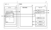
図7は、高分解能モードかつ相対モード(HAMODE=1、RELMODE=1)の場合の調光設定データDIMSETnの更新例を示す構成図である(図4に対応)。図7の例では、アドレスフレームAddressによりアドレス0x4Bが送信された場合を示す。
UARTインタフェース1に受信データRXが入力され、受信データ11Aがバッファ11に格納される。受信データ11Aには、アドレス0x4Bとともに、書き込みデータWDTが含まれる。書き込みデータWDTには、チャンネルCH01に対応する極性データCH01SG、ゲインデータCH01GAIN、および相対値データDUTY01が含まれる。この場合、相対計算部221において、下記のような計算が行われる。
DIMSET01=DIMSET01±DUTY01×CH01GAIN
DIMSET01=DIMSET01±DUTY01×CH01GAIN
上記のように計算されたチャンネルCH01の調光設定データDIMSET01の値により、レジスタ21における調光設定データDIMSET01の値が更新される。
なお、図7では図示を省略しているチャンネルCH02以降の調光設定データDIMSETnの更新も上記と同様に行われる。
次に、高分解能モードかつ絶対モード(HAMODE=1、RELMODE=0)に設定された場合の調光設定データの更新方法について説明する。
この場合、受信データRXにより次のような送信が行われる。レジスタ21のレジスタマップ(図5)において調光設定データの更新を所望する先頭チャンネルに対応するアドレスがアドレスフレームAddressに指定される。さらに、上記レジスタマップにおいて当該指定されたアドレスから連続したアドレスに対応する調光設定データDIMSETnが必要なチャンネル分だけデータフレームDataNにより送信される。
例えば図8Aは、更新を所望するチャンネルがチャンネルCH01のみである場合に受信データRXにより送信されるデータを示す。この場合、アドレスフレームAddressに0x4Bが指定され、DIMSET01の上位ビットがデータフレームData1により送信され、DIMSET01の下位ビットがデータフレームData2により送信される。この場合、チャンネルCH02のDIMSET02の下位ビットはダミーデータとされる。
また、例えば図8Bは、更新を所望するチャンネルがチャンネルCH01、CH02である場合に受信データRXにより送信されるデータを示す。この場合、アドレスフレームAddressに0x4Bが指定され、DIMSET01の上位ビットがデータフレームData1により送信され、DIMSET01の下位ビットおよびDIMSET02の下位ビットがデータフレームData2により送信され、DIMSET02の上位ビットがデータフレームData3により送信される。
また、例えば図8Cは、更新を所望するチャンネルがチャンネルCH02のみである場合に受信データRXにより送信されるデータを示す。この場合、アドレスフレームAddressに0x4Cが指定され、DIMSET02の下位ビットがデータフレームData1により送信され、DIMSET02の上位ビットがデータフレームData2により送信される。この場合、チャンネルCH01のDIMSET01の下位ビットはダミーデータとされる。
上記のように送信された調光設定データDIMSETnにより、レジスタ21における調光設定データDIMSETnが更新される。ただし、ダミーデータによってはレジスタ21のデータは更新されない。
図9は、高分解能モードかつ絶対モード(HAMODE=1、RELMODE=0)の場合の調光設定データDIMSETnの更新例を示す構成図である(図4に対応)。図9の例では、チャンネルCH01の調光設定データDIMSET01のみを更新する場合を示す。
UARTインタフェース1に受信データRXが入力され、受信データ11Aがバッファ11に格納される。受信データ11Aには、アドレス0x4Bとともに、書き込みデータWDTが含まれる。書き込みデータWDTには、DIMSET01の上位・下位ビット、およびDIMSET02の下位ビットが格納される(図8A)。これにより、更新制御部22は、アドレス0x4BおよびDIMSET01の上位・下位ビットに基づき、レジスタ21におけるDIMSET01を更新する。
上記のように本実施形態であれば、高分解能(例えば12ビット)である調光設定データDIMSETnを相対的あるいは絶対的に更新することが可能となる。ここで、図10は、グラデーション調光を行う場合のオンデューティの範囲と、オンデューティを変化させるステップとの対応関係の一例を示す図である。このように、デューティを高くするほど、ステップを大きくする。グラデーション調光では、オンデューティを現状値から目標値まで指定されたステップで増加させる。オンデューティを高分解能で表すことにより、最小ステップを小さくすることができる。このようなグラデーション調光などにおいては、必要なステップが小さいため、相対モードによる調光設定データの更新により調光が可能である。なお、オンデューティを大きく変化させる必要がある場合は、絶対モードを使用すればよい。
例えば、24チャンネル分の調光設定データを更新する場合、絶対モードであれば、24ch×12ビット=36バイトのデータ送信が必要となるが、相対モードであれば、24ch×8ビット=24バイトのデータ送信で済むことになり、通信量の低減が可能となる。特にPWM周波数が高い場合、通信量の低減がより有効となる。
また、図1に示すように、複数の半導体装置10の各RX端子10AをCANトランシーバ40の同一のRXD端子40Aに共通接続する場合に、複数の半導体装置10がLEDドライバICであるとする。この場合に、複数の半導体装置10のそれぞれにおいて調光設定データを更新する場合、シリアル通信により受信データRXを複数の半導体装置10のそれぞれに対して順に送信する必要があり、1回の送信における通信量を低減することが有効となる。
<<低分解能モードの場合>>
次に、分解能モードが低分解能モードに設定された場合(HAMODE=0)の調光設定データの更新方法について説明する。ここで、上記第2所定ビット数は一例として8ビットであるとする。
次に、分解能モードが低分解能モードに設定された場合(HAMODE=0)の調光設定データの更新方法について説明する。ここで、上記第2所定ビット数は一例として8ビットであるとする。
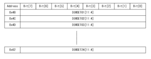
図11は、低分解能モードの場合のレジスタ21における調光設定データDIMSETnの格納を示す図(レジスタマップ)である。図11では、レジスタ21におけるアドレスと、当該アドレスに格納される調光設定データDIMSETnの対応関係を示す。
アドレス0x4Bから0x62までの連続した各アドレスには、それぞれ8ビットであるDIMSET01~DIMSET24のそれぞれが格納される。従って、低分解能モードでは、高分解能モード(図5)に対してレジスタマップを変更している。
この場合、受信データRXにより次のような送信が行われる。レジスタ21のレジスタマップ(図11)において調光設定データの更新を所望する先頭チャンネルに対応するアドレスがアドレスフレームAddressに指定される。さらに、上記レジスタマップにおいて当該指定されたアドレスから連続したアドレスに対応する調光設定データDIMSETnが必要なチャンネル分だけデータフレームDataNにより送信される。
例えば、24チャンネル分のデータを送信する場合は、アドレスフレームAddressに0x4Bが指定され、DIMSET01~DIMSET24がデータフレームData1~Data24により送信される。
図12は、低分解能モードかつ絶対モード(HAMODE=0、RELMODE=0)の場合の調光設定データDIMSETnの更新例を示す構成図である(図4に対応)。
図12の例では、UARTインタフェース1に受信データRXが入力され、受信データ11Aがバッファ11に格納される。受信データ11Aには、アドレス0x4Bとともに、書き込みデータWDTが含まれる。書き込みデータWDTには、DIMSET01、DIMSET02などが含まれる。これにより、更新制御部22は、アドレス0x4BおよびDIMSET01、DIMSET02などに基づき、レジスタ21におけるDIMSET01、DIMSET02などを更新する。
低分解能モードでは、図11に示すようなレジスタマップとすることで、アドレスフレームAddressによりアドレスを指定すれば、指定されたアドレスからインクリメントしたアドレスで調光設定データDIMSETnを更新することができる。すなわち、複数チャンネルの調光設定データDIMSETnを更新するときに、1回の受信データRXの送信により更新が可能となり、通信量を低減できる。
なお、低分解能モードでは、絶対的な更新であっても通信量を低減するので、相対モードには設定されない。
<5.グループ設定機能>
本実施形態の半導体装置10は、次に説明するようなグループ設定機能を有してもよい。
本実施形態の半導体装置10は、次に説明するようなグループ設定機能を有してもよい。
図13は、グループ設定機能に関するレジスタ21におけるレジスタマップを示す図である。図13の例では、アドレス0x32から0x37までの連続した各アドレスに対して、グループ設定データCHnDTYGRPが格納される。グループ設定データCHnDTYGRPは、2ビットのデータであり、チャンネルCHnにおけるグループ設定を示す。例えば、CHnDTYGRP=01の場合、第1グループに設定され、CHnDTYGRP=10の場合、第2グループに設定され、CHnDTYGRP=11の場合、第3グループに設定される。
図13では、具体的に、アドレス0x32に対して上位ビットから順に、CH04DTYGRP~CH01DTYGRPが格納され、アドレス0x33に対して上位ビットから順に、CH08DTYGRP~CH05DTYGRPが格納され、以降同様にCH24DTYGRPまで格納される。
図13では、アドレス0x38から0x3Cまでの連続した各アドレスに対して、デューティ設定値データDTYGRPmが格納される。デューティ設定値データDTYGRPmは、12ビットのデータであり、第mグループに設定されるオンデューティ値を示す。
図13では、具体的に、アドレス0x38に対してDTYGRP1の上位8ビットが格納され、アドレス0x39に対してDTYGRP2の下位4ビットとDTYGRP1の下位4ビットが格納され、アドレス0x3Aに対してDTYGRP2の上位8ビットが格納され、アドレス0x3Bに対してDTYGRP3の上位8ビットが格納され、アドレス0x3Cに対してDTYGRP3の下位4ビットが格納される。また、アドレス0x3Cには、全チャンネル更新モード設定データGRPALL(1ビット)が格納される。
受信データRXにおいては、アドレス0x32がアドレスフレームAddressに指定され、グループ設定データCH01DTYGRP~CH24DTYGRPに加えて、必要なグループ数に対するデューティ設定値データDTYGRPmがデータフレームDataNにより送信される。
上記のように受信データRXにより送信されたデータに基づき、レジスタ21におけるグループ設定データCH01DTYGRP~CH24DTYGRPおよびデューティ設定値データDTYGRPmが更新される。すると、グループ設定データCH01DTYGRP~CH24DTYGRPによりグループ分けされたチャンネルCHnの調光設定データDIMSETnが、グループごとに対応するデューティ設定値データDTYGRPmに基づいて更新される。
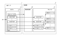
図14は、グループ設定機能を用いて調光設定データDIMSETnを更新する例を示す構成図である(図4に対応)。図14の例では、UARTインタフェース1に受信データRXが入力され、受信データ11Aがバッファ11に格納される。受信データ11Aには、アドレス0x32とともに、書き込みデータWDTが含まれる。書き込みデータWDTには、グループ設定データCH01DTYGRP~CH24DTYGRPおよびデューティ設定値データDTYGRP1,2が含まれる。すなわち、図14の例では、グループ分けするグループ数を2としている。
更新制御部22は、グループ設定データCH01DTYGRP~CH24DTYGRPに基づき、レジスタ21におけるグループ設定データCH01DTYGRP~CH24DTYGRPを更新するとともに、デューティ設定値データDTYGRP1,2に基づき、レジスタ12におけるデューティ設定値データDTYGRP1,2を更新する。
例えばグループ設定データCH01DTYGRP~CH24DTYGRPによってチャンネルCH01~08が第1グループ、チャンネルCH09~24が第2グループに設定された場合、図14に示すように、レジスタ21において、デューティ設定値データDTYGRP1により調光設定データDIMSET01~08が更新され、デューティ設定値データDTYGRP2により調光設定データDIMSET09~24が更新される。調光設定データの更新は、更新制御部22により行われる。
このようなグループ設定機能によれば、図14に示す例の場合、24チャンネル分の調光設定データの更新を行うために、グループ設定データCH01DTYGRP~CH24DTYGRPの送信による6バイト(=2ビット×24ch)に加えて、2つのグループ分のデューティ設定値データDTYGRP1,2の送信による3バイトが必要となり、合わせて9バイトの送信が必要である。これに対して、先述した高分解能モードかつ絶対モードの場合は、12ビット×24ch=36バイトの送信が必要となり、グループ設定機能の場合、通信量を低減できる。
なお、全チャンネル更新モード設定データGRPALLが例えば0の場合、グループ設定機能が有効となり、全チャンネル更新モードは無効となる。一方、GRPALLが例えば1の場合、グループ設定機能が無効となり、全チャンネル更新モードは有効となる。この場合、全チャンネル(24チャンネル)分の調光設定データDIMSETnが例えばDTYGRP3に基づいて同じ値に更新される。
<6.その他>
なお、本明細書中に開示されている種々の技術的特徴は、上記実施形態のほか、その技術的創作の主旨を逸脱しない範囲で種々の変更を加えることが可能である。すなわち、上記実施形態は、全ての点で例示であって制限的なものではないと考えられるべきであり、本開示の技術的範囲は、上記実施形態に限定されるものではなく、特許請求の範囲と均等の意味および範囲内に属する全ての変更が含まれると理解されるべきである。
なお、本明細書中に開示されている種々の技術的特徴は、上記実施形態のほか、その技術的創作の主旨を逸脱しない範囲で種々の変更を加えることが可能である。すなわち、上記実施形態は、全ての点で例示であって制限的なものではないと考えられるべきであり、本開示の技術的範囲は、上記実施形態に限定されるものではなく、特許請求の範囲と均等の意味および範囲内に属する全ての変更が含まれると理解されるべきである。
例えば、シリアル通信は、UART通信に限らず、I2C通信などであってもよい。
<7.付記>
以上のように、本開示の一態様に係る半導体装置(10)は、
シリアル通信により送信された書き込みデータ(WDT)を外部から受信するように構成されるインタフェース部(1)と、
前記書き込みデータに基づいて計算を行うように構成される相対計算部(221)を有する更新制御部(22)と、
PWMのデューティ値を示すデューティ設定データ(DIMSETn)が格納されるように構成されるレジスタ(21)と、
を備え、
前記書き込みデータは、
減少または増加を表す極性データ(CHnSG)と、
ゲイン値を表すゲインデータ(CHnGAIN)と、
相対変化値を表す相対値データ(DUTYn)と、
を含み、
前記相対計算部は、前記相対変化値に前記ゲイン値を乗算して得られる値を現状の前記デューティ設定データの値に対して、前記極性データに応じて減算または加算して計算結果を算出し、
前記更新制御部は、前記計算結果によって前記デューティ設定データを更新する構成としている(第1の構成)。
以上のように、本開示の一態様に係る半導体装置(10)は、
シリアル通信により送信された書き込みデータ(WDT)を外部から受信するように構成されるインタフェース部(1)と、
前記書き込みデータに基づいて計算を行うように構成される相対計算部(221)を有する更新制御部(22)と、
PWMのデューティ値を示すデューティ設定データ(DIMSETn)が格納されるように構成されるレジスタ(21)と、
を備え、
前記書き込みデータは、
減少または増加を表す極性データ(CHnSG)と、
ゲイン値を表すゲインデータ(CHnGAIN)と、
相対変化値を表す相対値データ(DUTYn)と、
を含み、
前記相対計算部は、前記相対変化値に前記ゲイン値を乗算して得られる値を現状の前記デューティ設定データの値に対して、前記極性データに応じて減算または加算して計算結果を算出し、
前記更新制御部は、前記計算結果によって前記デューティ設定データを更新する構成としている(第1の構成)。
このような構成によれば、PWMのデューティ値の更新を相対的に行うことができ、書き込みデータのデータ量を低減することができる。従って、PWM制御の設定時におけるシリアル通信の通信量を低減することを可能とする課題を解決できる。
また、上記第1の構成において、前記ゲインデータによって前記ゲイン値を1に設定可能である構成としてもよい(第2の構成)。
また、上記第1または第2の構成において、前記極性データのビット数と前記ゲインデータのビット数と前記相対値データのビット数を合わせたビット数(例えば8ビット)は、前記デューティ設定データの第1所定ビット数(例えば12ビット)よりも小さい構成としてもよい(第3の構成)。
また、上記第3の構成において、前記更新制御部が前記計算結果によって前記デューティ設定データを更新する相対モードと、
前記更新制御部が前記シリアル通信により送信された前記書き込みデータに含まれる前記第1所定ビット数の前記デューティ設定データによって前記レジスタに格納された前記デューティ設定データを更新する絶対モードと、
を有する構成としてもよい(第4の構成)。
前記更新制御部が前記シリアル通信により送信された前記書き込みデータに含まれる前記第1所定ビット数の前記デューティ設定データによって前記レジスタに格納された前記デューティ設定データを更新する絶対モードと、
を有する構成としてもよい(第4の構成)。
また、上記第3または第4の構成において、前記レジスタに格納された前記デューティ設定データが前記第1所定ビット数(例えば12ビット)である高分解能モードと、
前記レジスタに格納された前記デューティ設定データが前記第1所定ビット数よりも小さい第2所定ビット数(例えば8ビット)である低分解能モードと、
を有する構成としてもよい(第5の構成)。
前記レジスタに格納された前記デューティ設定データが前記第1所定ビット数よりも小さい第2所定ビット数(例えば8ビット)である低分解能モードと、
を有する構成としてもよい(第5の構成)。
また、上記第5の構成において、前記レジスタにおいて1つのアドレスに対して格納可能なデータのビット数は、前記第2所定ビット数であり、
前記高分解能モードの場合、前記レジスタにおいて、第1アドレス(例えば0x4B)に対して第1チャンネルの前記デューティ設定データの上位ビットが格納され、第1アドレスをインクリメントした第2アドレス(例えば0x4C)に対して前記第1チャンネルの前記デューティ設定データの下位ビットおよび第2チャンネルの前記デューティ設定データの下位ビットが格納され、前記第2アドレスをインクリメントした第3アドレス(例えば0x4D)に対して前記第2チャンネルの前記デューティ設定データの上位ビットが格納され、
前記低分解能モードの場合、前記レジスタにおいて、連続した各アドレスに対して各チャンネルの前記デューティ設定データがそれぞれ格納される構成としてもよい(第6の構成、図5および図11)。
前記高分解能モードの場合、前記レジスタにおいて、第1アドレス(例えば0x4B)に対して第1チャンネルの前記デューティ設定データの上位ビットが格納され、第1アドレスをインクリメントした第2アドレス(例えば0x4C)に対して前記第1チャンネルの前記デューティ設定データの下位ビットおよび第2チャンネルの前記デューティ設定データの下位ビットが格納され、前記第2アドレスをインクリメントした第3アドレス(例えば0x4D)に対して前記第2チャンネルの前記デューティ設定データの上位ビットが格納され、
前記低分解能モードの場合、前記レジスタにおいて、連続した各アドレスに対して各チャンネルの前記デューティ設定データがそれぞれ格納される構成としてもよい(第6の構成、図5および図11)。
また、上記第1から第6のいずれかの構成において、前記レジスタにおいて、複数チャンネルの前記デューティ設定データが格納され、
前記極性データ、前記ゲインデータ、および前記相対値データは、前記複数チャンネルに対応する構成としてもよい(第7の構成)。
前記極性データ、前記ゲインデータ、および前記相対値データは、前記複数チャンネルに対応する構成としてもよい(第7の構成)。
また、上記第1から第7のいずれかの構成において、前記デューティ設定データに基づいてPWM調光を行うことが可能である構成としてもよい(第8の構成)。
また、上記第8の構成において、前記PWM調光のオンデューティが高いほど、前記オンデューティを変化させるステップが大きく、前記オンデューティを前記ステップに従って増加させるグラデーション調光が可能である構成としてもよい(第9の構成)。
また、上記第1から第9のいずれかの構成において、前記レジスタにおいて、複数チャンネルの前記デューティ設定データが格納され、
前記複数チャンネルのチャンネルごとにグループを設定するためのグループ設定データ(CHnDTYGRP)と、前記グループごとの前記デューティ値を設定するためのデューティ設定値データ(DTYGRPm)とが前記書き込みデータに含まれる場合、前記更新制御部は、前記デューティ設定データを前記グループ設定データおよび前記デューティ設定値データに基づいて更新する構成としてもよい(第10の構成)。
前記複数チャンネルのチャンネルごとにグループを設定するためのグループ設定データ(CHnDTYGRP)と、前記グループごとの前記デューティ値を設定するためのデューティ設定値データ(DTYGRPm)とが前記書き込みデータに含まれる場合、前記更新制御部は、前記デューティ設定データを前記グループ設定データおよび前記デューティ設定値データに基づいて更新する構成としてもよい(第10の構成)。
また、上記第10の構成において、前記デューティ設定データを前記グループ設定データおよび前記デューティ設定値データに基づいて更新するモードと、
前記複数チャンネルのすべてのチャンネルに対応する前記デューティ設定データを、所定の前記グループに対応する前記デューティ設定値データに基づいて更新するモードと、を切り替え可能である構成としてもよい(第11の構成)。
前記複数チャンネルのすべてのチャンネルに対応する前記デューティ設定データを、所定の前記グループに対応する前記デューティ設定値データに基づいて更新するモードと、を切り替え可能である構成としてもよい(第11の構成)。
また、上記第1から第11のいずれかの構成において、前記シリアル通信は、UART通信である構成としてもよい(第12の構成)。
また、本開示の一態様に係る通信システム(501)は、上記第1から第12のいずれかの構成の半導体装置(10)と、前記書き込みデータを送信するように構成される送信装置(40)と、を備える構成としている(第13の構成)。
また、上記第13の構成において、複数の前記半導体装置のそれぞれに備えられ、前記書き込みデータが入力されるように構成される入力端子(10A)は、前記送信装置に備えられる同一の出力端子(40A)に共通接続される構成としてもよい(第14の構成)。
本開示は、例えば、車載用の通信システムに利用することが可能である。
1 UARTインタフェース
2 制御部
3 PWM生成部
4 電流ドライバ
6 LED
10 半導体装置
10A RX端子
10B TX端子
10C カソード端子
11 バッファ
11A 受信データ
21 レジスタ
22 更新制御部
30,40 CANトランシーバ
30A TXD端子
30B RXD端子
35 CANバス
40A RXD端子
40B TXD端子
221 相対計算部
501 通信システム
2 制御部
3 PWM生成部
4 電流ドライバ
6 LED
10 半導体装置
10A RX端子
10B TX端子
10C カソード端子
11 バッファ
11A 受信データ
21 レジスタ
22 更新制御部
30,40 CANトランシーバ
30A TXD端子
30B RXD端子
35 CANバス
40A RXD端子
40B TXD端子
221 相対計算部
501 通信システム
Claims (14)
- シリアル通信により送信された書き込みデータを外部から受信するように構成されるインタフェース部と、
前記書き込みデータに基づいて計算を行うように構成される相対計算部を有する更新制御部と、
PWMのデューティ値を示すデューティ設定データが格納されるように構成されるレジスタと、
を備え、
前記書き込みデータは、
減少または増加を表す極性データと、
ゲイン値を表すゲインデータと、
相対変化値を表す相対値データと、
を含み、
前記相対計算部は、前記相対変化値に前記ゲイン値を乗算して得られる値を現状の前記デューティ設定データの値に対して、前記極性データに応じて減算または加算して計算結果を算出し、
前記更新制御部は、前記計算結果によって前記デューティ設定データを更新する、半導体装置。 - 前記ゲインデータによって前記ゲイン値を1に設定可能である、請求項1に記載の半導体装置。
- 前記極性データのビット数と前記ゲインデータのビット数と前記相対値データのビット数を合わせたビット数は、前記デューティ設定データの第1所定ビット数よりも小さい、請求項1または請求項2に記載の半導体装置。
- 前記更新制御部が前記計算結果によって前記デューティ設定データを更新する相対モードと、
前記更新制御部が前記シリアル通信により送信された前記書き込みデータに含まれる前記第1所定ビット数の前記デューティ設定データによって前記レジスタに格納された前記デューティ設定データを更新する絶対モードと、
を有する、請求項3に記載の半導体装置。 - 前記レジスタに格納された前記デューティ設定データが前記第1所定ビット数である高分解能モードと、
前記レジスタに格納された前記デューティ設定データが前記第1所定ビット数よりも小さい第2所定ビット数である低分解能モードと、
を有する、請求項3または請求項4に記載の半導体装置。 - 前記レジスタにおいて1つのアドレスに対して格納可能なデータのビット数は、前記第2所定ビット数であり、
前記高分解能モードの場合、前記レジスタにおいて、第1アドレスに対して第1チャンネルの前記デューティ設定データの上位ビットが格納され、第1アドレスをインクリメントした第2アドレスに対して前記第1チャンネルの前記デューティ設定データの下位ビットおよび第2チャンネルの前記デューティ設定データの下位ビットが格納され、前記第2アドレスをインクリメントした第3アドレスに対して前記第2チャンネルの前記デューティ設定データの上位ビットが格納され、
前記低分解能モードの場合、前記レジスタにおいて、連続した各アドレスに対して各チャンネルの前記デューティ設定データがそれぞれ格納される、請求項5に記載の半導体装置。 - 前記レジスタにおいて、複数チャンネルの前記デューティ設定データが格納され、
前記極性データ、前記ゲインデータ、および前記相対値データは、前記複数チャンネルに対応する、請求項1から請求項6のいずれか1項に記載の半導体装置。 - 前記デューティ設定データに基づいてPWM調光を行うことが可能である、請求項1から請求項7のいずれか1項に記載の半導体装置。
- 前記PWM調光のオンデューティが高いほど、前記オンデューティを変化させるステップが大きく、前記オンデューティを前記ステップに従って増加させるグラデーション調光が可能である、請求項8に記載の半導体装置。
- 前記レジスタにおいて、複数チャンネルの前記デューティ設定データが格納され、
前記複数チャンネルのチャンネルごとにグループを設定するためのグループ設定データと、前記グループごとの前記デューティ値を設定するためのデューティ設定値データとが前記書き込みデータに含まれる場合、前記更新制御部は、前記デューティ設定データを前記グループ設定データおよび前記デューティ設定値データに基づいて更新する、請求項1から請求項9のいずれか1項に記載の半導体装置。 - 前記デューティ設定データを前記グループ設定データおよび前記デューティ設定値データに基づいて更新するモードと、
前記複数チャンネルのすべてのチャンネルに対応する前記デューティ設定データを、所定の前記グループに対応する前記デューティ設定値データに基づいて更新するモードと、を切り替え可能である、請求項10に記載の半導体装置。 - 前記シリアル通信は、UART通信である、請求項1から請求項11のいずれか1項に記載の半導体装置。
- 請求項1から請求項12のいずれか1項に記載の半導体装置と、前記書き込みデータを送信するように構成される送信装置と、を備える、通信システム。
- 複数の前記半導体装置のそれぞれに備えられ、前記書き込みデータが入力されるように構成される入力端子は、前記送信装置に備えられる同一の出力端子に共通接続される、請求項13に記載の通信システム。
Priority Applications (2)
| Application Number | Priority Date | Filing Date | Title |
|---|---|---|---|
| CN202480043730.1A CN121533139A (zh) | 2023-07-06 | 2024-06-07 | 半导体装置以及通信系统 |
| JP2025531441A JPWO2025009328A1 (ja) | 2023-07-06 | 2024-06-07 |
Applications Claiming Priority (2)
| Application Number | Priority Date | Filing Date | Title |
|---|---|---|---|
| JP2023-111348 | 2023-07-06 | ||
| JP2023111348 | 2023-07-06 |
Publications (1)
| Publication Number | Publication Date |
|---|---|
| WO2025009328A1 true WO2025009328A1 (ja) | 2025-01-09 |
Family
ID=94171893
Family Applications (1)
| Application Number | Title | Priority Date | Filing Date |
|---|---|---|---|
| PCT/JP2024/020847 Ceased WO2025009328A1 (ja) | 2023-07-06 | 2024-06-07 | 半導体装置、および通信システム |
Country Status (3)
| Country | Link |
|---|---|
| JP (1) | JPWO2025009328A1 (ja) |
| CN (1) | CN121533139A (ja) |
| WO (1) | WO2025009328A1 (ja) |
Cited By (1)
| Publication number | Priority date | Publication date | Assignee | Title |
|---|---|---|---|---|
| US20250016023A1 (en) * | 2023-07-05 | 2025-01-09 | Rohm Co., Ltd. | Semiconductor device and communication system |
Citations (2)
| Publication number | Priority date | Publication date | Assignee | Title |
|---|---|---|---|---|
| JP2009526365A (ja) * | 2006-02-10 | 2009-07-16 | フィリップス ソリッド−ステート ライティング ソリューションズ インコーポレイテッド | 負荷当たり単一のスイッチング段を使用した高力率の制御された電力供給のための方法及び装置 |
| JP2017506569A (ja) * | 2014-02-14 | 2017-03-09 | アプライド バイオフォトニクス リミテッド | 光線治療のための正弦波駆動システム及び方法 |
-
2024
- 2024-06-07 CN CN202480043730.1A patent/CN121533139A/zh active Pending
- 2024-06-07 WO PCT/JP2024/020847 patent/WO2025009328A1/ja not_active Ceased
- 2024-06-07 JP JP2025531441A patent/JPWO2025009328A1/ja active Pending
Patent Citations (2)
| Publication number | Priority date | Publication date | Assignee | Title |
|---|---|---|---|---|
| JP2009526365A (ja) * | 2006-02-10 | 2009-07-16 | フィリップス ソリッド−ステート ライティング ソリューションズ インコーポレイテッド | 負荷当たり単一のスイッチング段を使用した高力率の制御された電力供給のための方法及び装置 |
| JP2017506569A (ja) * | 2014-02-14 | 2017-03-09 | アプライド バイオフォトニクス リミテッド | 光線治療のための正弦波駆動システム及び方法 |
Cited By (2)
| Publication number | Priority date | Publication date | Assignee | Title |
|---|---|---|---|---|
| US20250016023A1 (en) * | 2023-07-05 | 2025-01-09 | Rohm Co., Ltd. | Semiconductor device and communication system |
| US12549409B2 (en) * | 2023-07-05 | 2026-02-10 | Rohm Co., Ltd. | Semiconductor device and communication system for updating setting data of multiple channels |
Also Published As
| Publication number | Publication date |
|---|---|
| JPWO2025009328A1 (ja) | 2025-01-09 |
| CN121533139A (zh) | 2026-02-13 |
Similar Documents
| Publication | Publication Date | Title |
|---|---|---|
| US8183789B2 (en) | Lighting system for avionics applications and control method thereof | |
| EP2478650B1 (en) | Apparatus and method for generating high resolution frames for dimming and visibility support in visible light communication | |
| CN1171417C (zh) | 处理通信系统中不同类型的消息的方法和设备 | |
| CN106464368A (zh) | 使用可见光通信传输识别符 | |
| WO2025009328A1 (ja) | 半導体装置、および通信システム | |
| US20250021513A1 (en) | Synchronization signal transmission method and serial communication system | |
| US20260121753A1 (en) | Signal transmission method and device, storage medium, and electronic device | |
| CN1802880B (zh) | 用于数据传输的光输出调制 | |
| EP4092971A1 (en) | Bus controlled lighting system | |
| JP2025008610A (ja) | 半導体装置、および通信システム | |
| CN105208021A (zh) | 一种数据通讯方法及其系统 | |
| JP4785929B2 (ja) | 光伝送システムにおける電気等化による光信号のジッタ低減 | |
| JP6771791B2 (ja) | エネルギー効率の高いデータフレーム交換 | |
| US12388689B2 (en) | Coding module for a transceiver | |
| CN1750723A (zh) | 半导体照明远程调光控制装置 | |
| US20080031200A1 (en) | Wlan device and method for numbering frames with sequence numbers | |
| CN113411161B (zh) | 光调顶电路及方法 | |
| KR20160136621A (ko) | 발광다이오드 조명장치 및 그 제어방법 | |
| CN106950890B (zh) | 基于双485通讯的智能开关电路 | |
| WO2014205926A1 (zh) | 一种实现调光的方法及调光装置 | |
| CN219609996U (zh) | 背光驱动电路、背光模组及显示设备 | |
| CN115441953A (zh) | 基于otn传送技术的光发射芯片 | |
| US7127177B1 (en) | Integrated post-amplifier and laser driver assembly with digital control interface | |
| CN105050274A (zh) | 一种舞台多路调光系统 | |
| US20250202522A1 (en) | Subscriber station for a serial bus system, and method for communication with differential signals in a serial bus system |
Legal Events
| Date | Code | Title | Description |
|---|---|---|---|
| 121 | Ep: the epo has been informed by wipo that ep was designated in this application |
Ref document number: 24835846 Country of ref document: EP Kind code of ref document: A1 |
|
| ENP | Entry into the national phase |
Ref document number: 2025531441 Country of ref document: JP Kind code of ref document: A |
|
| WWE | Wipo information: entry into national phase |
Ref document number: 2025531441 Country of ref document: JP |
|
| NENP | Non-entry into the national phase |
Ref country code: DE |