WO2025005103A1 - センサおよび位置検出装置 - Google Patents
センサおよび位置検出装置 Download PDFInfo
- Publication number
- WO2025005103A1 WO2025005103A1 PCT/JP2024/023084 JP2024023084W WO2025005103A1 WO 2025005103 A1 WO2025005103 A1 WO 2025005103A1 JP 2024023084 W JP2024023084 W JP 2024023084W WO 2025005103 A1 WO2025005103 A1 WO 2025005103A1
- Authority
- WO
- WIPO (PCT)
- Prior art keywords
- sensor
- electrode
- pen
- electrode layer
- layer
- Prior art date
- Legal status (The legal status is an assumption and is not a legal conclusion. Google has not performed a legal analysis and makes no representation as to the accuracy of the status listed.)
- Ceased
Links
Images



Classifications
-
- G—PHYSICS
- G06—COMPUTING OR CALCULATING; COUNTING
- G06F—ELECTRIC DIGITAL DATA PROCESSING
- G06F3/00—Input arrangements for transferring data to be processed into a form capable of being handled by the computer; Output arrangements for transferring data from processing unit to output unit, e.g. interface arrangements
- G06F3/01—Input arrangements or combined input and output arrangements for interaction between user and computer
- G06F3/03—Arrangements for converting the position or the displacement of a member into a coded form
- G06F3/041—Digitisers, e.g. for touch screens or touch pads, characterised by the transducing means
- G06F3/044—Digitisers, e.g. for touch screens or touch pads, characterised by the transducing means by capacitive means
- G06F3/0442—Digitisers, e.g. for touch screens or touch pads, characterised by the transducing means by capacitive means using active external devices, e.g. active pens, for transmitting changes in electrical potential to be received by the digitiser
-
- G—PHYSICS
- G06—COMPUTING OR CALCULATING; COUNTING
- G06F—ELECTRIC DIGITAL DATA PROCESSING
- G06F3/00—Input arrangements for transferring data to be processed into a form capable of being handled by the computer; Output arrangements for transferring data from processing unit to output unit, e.g. interface arrangements
- G06F3/01—Input arrangements or combined input and output arrangements for interaction between user and computer
- G06F3/03—Arrangements for converting the position or the displacement of a member into a coded form
- G06F3/041—Digitisers, e.g. for touch screens or touch pads, characterised by the transducing means
-
- G—PHYSICS
- G06—COMPUTING OR CALCULATING; COUNTING
- G06F—ELECTRIC DIGITAL DATA PROCESSING
- G06F3/00—Input arrangements for transferring data to be processed into a form capable of being handled by the computer; Output arrangements for transferring data from processing unit to output unit, e.g. interface arrangements
- G06F3/01—Input arrangements or combined input and output arrangements for interaction between user and computer
- G06F3/03—Arrangements for converting the position or the displacement of a member into a coded form
- G06F3/041—Digitisers, e.g. for touch screens or touch pads, characterised by the transducing means
- G06F3/0416—Control or interface arrangements specially adapted for digitisers
- G06F3/04164—Connections between sensors and controllers, e.g. routing lines between electrodes and connection pads
-
- G—PHYSICS
- G06—COMPUTING OR CALCULATING; COUNTING
- G06F—ELECTRIC DIGITAL DATA PROCESSING
- G06F3/00—Input arrangements for transferring data to be processed into a form capable of being handled by the computer; Output arrangements for transferring data from processing unit to output unit, e.g. interface arrangements
- G06F3/01—Input arrangements or combined input and output arrangements for interaction between user and computer
- G06F3/03—Arrangements for converting the position or the displacement of a member into a coded form
- G06F3/041—Digitisers, e.g. for touch screens or touch pads, characterised by the transducing means
- G06F3/0416—Control or interface arrangements specially adapted for digitisers
- G06F3/04166—Details of scanning methods, e.g. sampling time, grouping of sub areas or time sharing with display driving
-
- G—PHYSICS
- G06—COMPUTING OR CALCULATING; COUNTING
- G06F—ELECTRIC DIGITAL DATA PROCESSING
- G06F3/00—Input arrangements for transferring data to be processed into a form capable of being handled by the computer; Output arrangements for transferring data from processing unit to output unit, e.g. interface arrangements
- G06F3/01—Input arrangements or combined input and output arrangements for interaction between user and computer
- G06F3/03—Arrangements for converting the position or the displacement of a member into a coded form
- G06F3/041—Digitisers, e.g. for touch screens or touch pads, characterised by the transducing means
- G06F3/044—Digitisers, e.g. for touch screens or touch pads, characterised by the transducing means by capacitive means
-
- G—PHYSICS
- G06—COMPUTING OR CALCULATING; COUNTING
- G06F—ELECTRIC DIGITAL DATA PROCESSING
- G06F3/00—Input arrangements for transferring data to be processed into a form capable of being handled by the computer; Output arrangements for transferring data from processing unit to output unit, e.g. interface arrangements
- G06F3/01—Input arrangements or combined input and output arrangements for interaction between user and computer
- G06F3/03—Arrangements for converting the position or the displacement of a member into a coded form
- G06F3/041—Digitisers, e.g. for touch screens or touch pads, characterised by the transducing means
- G06F3/044—Digitisers, e.g. for touch screens or touch pads, characterised by the transducing means by capacitive means
- G06F3/0445—Digitisers, e.g. for touch screens or touch pads, characterised by the transducing means by capacitive means using two or more layers of sensing electrodes, e.g. using two layers of electrodes separated by a dielectric layer
-
- G—PHYSICS
- G06—COMPUTING OR CALCULATING; COUNTING
- G06F—ELECTRIC DIGITAL DATA PROCESSING
- G06F3/00—Input arrangements for transferring data to be processed into a form capable of being handled by the computer; Output arrangements for transferring data from processing unit to output unit, e.g. interface arrangements
- G06F3/01—Input arrangements or combined input and output arrangements for interaction between user and computer
- G06F3/03—Arrangements for converting the position or the displacement of a member into a coded form
- G06F3/041—Digitisers, e.g. for touch screens or touch pads, characterised by the transducing means
- G06F3/044—Digitisers, e.g. for touch screens or touch pads, characterised by the transducing means by capacitive means
- G06F3/0446—Digitisers, e.g. for touch screens or touch pads, characterised by the transducing means by capacitive means using a grid-like structure of electrodes in at least two directions, e.g. using row and column electrodes
-
- G—PHYSICS
- G06—COMPUTING OR CALCULATING; COUNTING
- G06F—ELECTRIC DIGITAL DATA PROCESSING
- G06F3/00—Input arrangements for transferring data to be processed into a form capable of being handled by the computer; Output arrangements for transferring data from processing unit to output unit, e.g. interface arrangements
- G06F3/01—Input arrangements or combined input and output arrangements for interaction between user and computer
- G06F3/03—Arrangements for converting the position or the displacement of a member into a coded form
- G06F3/041—Digitisers, e.g. for touch screens or touch pads, characterised by the transducing means
- G06F3/044—Digitisers, e.g. for touch screens or touch pads, characterised by the transducing means by capacitive means
- G06F3/0448—Details of the electrode shape, e.g. for enhancing the detection of touches, for generating specific electric field shapes, for enhancing display quality
-
- G—PHYSICS
- G06—COMPUTING OR CALCULATING; COUNTING
- G06F—ELECTRIC DIGITAL DATA PROCESSING
- G06F3/00—Input arrangements for transferring data to be processed into a form capable of being handled by the computer; Output arrangements for transferring data from processing unit to output unit, e.g. interface arrangements
- G06F3/01—Input arrangements or combined input and output arrangements for interaction between user and computer
- G06F3/03—Arrangements for converting the position or the displacement of a member into a coded form
- G06F3/041—Digitisers, e.g. for touch screens or touch pads, characterised by the transducing means
- G06F3/046—Digitisers, e.g. for touch screens or touch pads, characterised by the transducing means by electromagnetic means
-
- G—PHYSICS
- G06—COMPUTING OR CALCULATING; COUNTING
- G06F—ELECTRIC DIGITAL DATA PROCESSING
- G06F2203/00—Indexing scheme relating to G06F3/00 - G06F3/048
- G06F2203/041—Indexing scheme relating to G06F3/041 - G06F3/045
- G06F2203/04106—Multi-sensing digitiser, i.e. digitiser using at least two different sensing technologies simultaneously or alternatively, e.g. for detecting pen and finger, for saving power or for improving position detection
-
- G—PHYSICS
- G06—COMPUTING OR CALCULATING; COUNTING
- G06F—ELECTRIC DIGITAL DATA PROCESSING
- G06F2203/00—Indexing scheme relating to G06F3/00 - G06F3/048
- G06F2203/041—Indexing scheme relating to G06F3/041 - G06F3/045
- G06F2203/04112—Electrode mesh in capacitive digitiser: electrode for touch sensing is formed of a mesh of very fine, normally metallic, interconnected lines that are almost invisible to see. This provides a quite large but transparent electrode surface, without need for ITO or similar transparent conductive material
-
- G—PHYSICS
- G06—COMPUTING OR CALCULATING; COUNTING
- G06F—ELECTRIC DIGITAL DATA PROCESSING
- G06F2203/00—Indexing scheme relating to G06F3/00 - G06F3/048
- G06F2203/041—Indexing scheme relating to G06F3/041 - G06F3/045
- G06F2203/04113—Peripheral electrode pattern in resistive digitisers, i.e. electrodes at the periphery of the resistive sheet are shaped in patterns enhancing linearity of induced field
Definitions
- the present invention relates to a sensor and a position detection device.
- This position input device is composed of a pen-shaped position indicator (pen-type position indicator) and a position detection device having an input surface on which pointing operations and input of characters, figures, etc. are performed using this pen-type position indicator.
- the position indicator includes a resonant circuit consisting of a coil and a capacitor.
- the position detection device in order to obtain the coordinate of the position indicator in the X-axis direction within the active area AA, the position detection device an X sensor coil group including X sensor coils X0, . . . , X4 arranged in the X direction; A switch connected to the X sensor coil group; During the sending period, an alternating magnetic field (a sending magnetic field, the same applies below) is generated by passing a current through each of the X sensor coils arranged on the X axis.
- an X-axis TX/RX circuit for detecting, in a detection period following the transmission period, an electromotive force generated in each of the X sensor coils by a pen signal (an alternating magnetic field generated by a circuit of the position indicator, the same applies below) which is continuously generated from the position indicator that has stored energy in its resonant circuit during the transmission period, as a current or voltage;
- the present invention is configured to include the following.
- the position detection device A Y sensor coil group including Y sensor coils Y0, . . . , Y4 arranged in the Y direction; A switch connected to the Y sensor coil group; During the transmission period, a transmission magnetic field is generated by passing a current through each of the X sensor coils arranged on the Y axis.
- a Y-axis TX/RX circuit that detects, in a detection period following the transmission period, an electromotive force generated in each of the Y sensor coils by a pen signal that is continuously generated from the position indicator that has stored energy in the resonant circuit during the transmission period, as a current or voltage;
- the present invention is configured to include the following.
- the position detection device selects one sensor coil in a predetermined order from a plurality of sensor coils that constitute a position detection sensor, sends a transmission signal from the selected sensor coil to a position indicator, and charges a capacitor in the position indicator.
- the position detection device receives the signal transmitted from the resonant circuit of the position indicator by connecting the sensor coil used for transmission to a receiving circuit.
- the position detection device detects the position of the position indicator on the position detection device by sequentially switching the sensor coils to transmit and receive such signals.
- a global scan is performed to detect where the position indicator is located on the indicated position detection sensor by sequentially switching all sensor coils to detect the indicated position of the position indicator, and the approximate position on the position detection sensor is identified
- a sector scan is performed to select in sequence only a predetermined number of sensor coils in the vicinity of the identified approximate position to send and receive signals, and the position indicated by the position indicator is accurately identified.
- the coordinate of the position indicator in the Y-axis direction is derived by interpolation or the like from the distribution of uniaxial level values, such as the level value 34 obtained by the Y sensor coil Y0, the level value 118 obtained by the Y sensor coil Y1, ... and the level value 107 obtained by the Y sensor coil Y4, as shown by RXdata (top row) in the figure.
- the X-axis coordinate of the position indicator is derived by interpolation or other calculations from the distribution of uniaxial level values, such as the level value 25 obtained by X sensor coil X0, the level value 100 obtained by X1, ..., and the level value 99 obtained by X4, as shown by RXdata (lower row) in the figure.
- the levels on each of the two axes are acquired separately, and the coordinates are determined for each dimension on each of the X and Y axes using the respective distributions (RXdata), and these two are combined and output as two-dimensional coordinates after certain processing.
- a stack configuration is as shown in FIG. 19, in which a display 300 (comprising a display front panel layer 301 and a TFT back panel layer 302) is provided, and an EMR sensor consisting of a TX sensor coil group 100 and an RX sensor coil group 200 is provided on the underside of the display 300 via an adhesive layer (Glue). Furthermore, a touch sensor is provided on the upper side of the display 300, and a cover glass (which may be a cover film; the same applies below) that comes into contact with the pen is provided on the upper side of the touch sensor (see, for example, Patent Document 1).
- the touch sensor, display 300, and EMR sensor including the TX sensor coil group 100 and the RX sensor coil group 200
- the touch sensor, display 300, and EMR sensor were each constructed on separate substrates (separate layers), which resulted in a problem that the thickness of the stack structure in which these were bonded together with an adhesive layer was large, impairing the design.
- the present invention was made in consideration of the above-mentioned problems, and aims to provide a sensor and a position detection device including the sensor that maintains the performance of the position detection device while thinning the stack structure and improving design.
- One or more embodiments of the present invention include an on-cell mutual capacitance touch sensor, and an RX electrode layer in which a plurality of RX electrodes are arranged to detect a pen alternating magnetic field generated by a pen that stores energy due to an alternating magnetic field from a TX electrode layer provided with a TX electrode that generates an alternating magnetic field for detecting the position of a pen using electromagnetic induction, and the RX electrode layer is surrounded by a touch electrode formed by a mesh electrode pattern provided on the on-cell touch layer of the on-cell mutual capacitance touch sensor, and the sensor proposes a sensor in which adjacent floating patterns in the extension direction of the RX electrodes are connected by jumper wiring to form a linear RX electrode wiring.
- Form 2 One or more embodiments of the present invention propose a sensor that includes an on-cell mutual capacitance touch sensor and an electromagnetic induction sensor, in which a first electrode group constituting the on-cell mutual capacitance touch sensor and a second electrode group constituting the electromagnetic induction sensor are composed of three or less layers, including a layer in which at least a portion of the first electrode group and a portion of the second electrode group are mixed.
- One or more embodiments of the present invention are a position detection device that detects the position of a pen using electromagnetic induction, and includes a TX electrode layer provided with a TX electrode that generates an alternating magnetic field, an RX electrode layer provided with a plurality of RX electrodes that detect a pen alternating magnetic field generated by a pen that accumulates energy by the alternating magnetic field, an on-cell mutual capacitance touch sensor, a display that controls display pixels and the blinking of the display pixels, and a support plate provided below the pen and away from the display, and the RX electrode layer is surrounded by a touch electrode formed by a mesh electrode pattern provided on the on-cell touch layer of the on-cell mutual capacitance touch sensor, and the floating patterns adjacent in the extension direction of the RX electrodes are connected by jumper wiring to form the RX electrodes in a straight line.
- FIG. 1 is a diagram illustrating an arrangement of touch sensors in a sensor according to a first embodiment of the present invention
- 3A to 3C are diagrams showing an arrangement pattern of a mesh electrode layer on a transparent substrate of a touch sensor in the sensor according to the first embodiment of the present invention.
- 4A and 4B are diagrams showing jumper wiring on the rear surface of a transparent substrate of a touch sensor in the sensor according to the first embodiment of the present invention.
- 4 is a diagram showing the mesh electrode layer of FIG. 2 and the jumper wiring of FIG. 3 superimposed in the sensor according to the first embodiment of the present invention.
- FIG. 1 is a diagram showing an operation mode when detecting electrostatic capacitance (finger touch) by an electrostatic capacitance detection method using the sensor according to the first embodiment of the present invention.
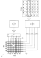
- FIG. 1 is a diagram showing an example of the configuration of a TX sensor coil group in a position detection device using a sensor according to a first embodiment of the present invention
- 11 is a diagram showing an operation mode process for performing pen detection by electromagnetic induction using the sensor according to the first embodiment of the present invention.
- FIG. This figure shows an example of a stack configuration in a sensor according to a second embodiment of the present invention, in which a position detection sensor, a touch sensor for detecting a finger or the like using a capacitance (self-capacitance or mutual capacitance) method, and a display device are combined (or incorporated).
- FIG. 11 is a diagram showing a configuration of a sensor according to a second embodiment of the present invention.
- FIGS. 13A and 13B are diagrams illustrating an operation mode process when a pen detection position is detected by an electromagnetic induction method using a sensor according to a second embodiment of the present invention.
- 10A and 10B are conceptual diagrams showing a coordinate deriving operation of a position detection device according to a second embodiment of the present invention.
- FIG. 10 is a diagram showing a wiring configuration in a modified example of the sensor according to the second embodiment of the present invention.
- FIG. 10 is a diagram showing a wiring configuration in a modified example of the sensor according to the second embodiment of the present invention.
- 13A and 13B are conceptual diagrams showing a coordinate deriving operation in a modified example of the position detection device according to the third embodiment of the present invention.
- FIG. 13 is a diagram showing an example of the configuration of a TX sensor coil group in a position detection device according to a fourth embodiment of the present invention.
- FIG. 13 is a diagram showing an example of the configuration of a TX sensor coil group in a position detection device according to a fourth embodiment of the present invention.
- FIG. 13 is a diagram showing an example of the configuration of a TX sensor coil group in a position detection device according to a fifth embodiment of the present invention.
- FIG. 13 is a conceptual diagram showing a coordinate deriving operation of a position detection device according to a conventional example.
- FIG. 1 is a diagram showing a conventional stack configuration in which a position detection device according to a conventional example, a touch sensor for detecting a finger or the like using a capacitance (self-capacitance or mutual capacitance) method, and a display device are combined (or incorporated).
- FIG. 1 First Embodiment A sensor 1 according to this embodiment will be described with reference to FIGS. 1 to 7.
- FIG. 1 A sensor 1 according to this embodiment will be described with reference to FIGS. 1 to 7.
- the sensor 1 of this embodiment is configured to include an on-cell type mutual capacitance touch sensor TS1 and an RX electrode layer (RX sensor coil group 200) for detecting the position of the pen by using electromagnetic induction.
- the on-cell mutual capacitance touch sensor TS1 is an integrated/universal sensor module provided on top of a laminate of a TFT back panel layer 302 and a display front panel layer 301, as shown in FIG.
- the on-cell mutual capacitance touch sensor TS1 is provided, for example, between the display front panel layer 301 and a glass substrate provided with a polarizing plate and a color filter (not shown) on the upper part of the display front panel layer 301.
- the on-cell mutual capacitance touch sensor TS1 is, for example, a mutual capacitance touch sensor.
- the RX electrode layer (RX sensor coil group 200) is a sensor that detects the pen alternating magnetic field generated by a pen that accumulates energy due to the alternating magnetic field from the TX electrode layer provided with TX electrodes that generate an alternating magnetic field for detecting the position of the pen using electromagnetic induction, and the RX electrode layer (RX sensor coil group 200) has multiple RX electrodes arranged thereon.
- the detailed configuration of the RX electrode layer (RX sensor coil group 200) for detecting the position of the pen by using electromagnetic induction will be described later.
- the sensor 1 is formed by integrating an RX electrode layer (RX sensor coil group 200) for detecting the position of a pen using electromagnetic induction into a mesh electrode pattern provided on the on-cell touch layer of an on-cell mutual capacitance touch sensor TS1, as shown in FIG. 4, for example.
- RX sensor coil group 200 for detecting the position of a pen using electromagnetic induction into a mesh electrode pattern provided on the on-cell touch layer of an on-cell mutual capacitance touch sensor TS1, as shown in FIG. 4, for example.
- the on-cell mutual capacitance touch sensor TS1 includes a plurality of first sensor electrodes (TX electrodes for touch panel) 210 and a plurality of second sensor electrodes 220 (RX electrode layers for touch panel).
- the plurality of first sensor electrodes (TX electrodes for touch panel) 210 and the plurality of second sensor electrodes 220 (RX electrode layers for touch panel) are superimposed on a display area (not shown).
- a plurality of first sensor electrodes 210 are arranged in the direction D1 shown in FIG.
- the first sensor electrode 210 has, for example, a diamond shape made up of a floating pattern 611 and a peripheral portion 612 surrounding the periphery of the floating pattern 611 .
- the peripheral portion 612 of the first sensor electrode 210 is connected to the peripheral portion 612 of the adjacent first sensor electrode 210 in the D1 direction by a mesh connection portion 613 to form a first touch sensor wiring (T0 to T4).
- the mesh connection portion 613 is formed from the same material as the first sensor electrode 210 .
- the first sensor electrode 210 is insulated in the mesh electrode layer from mesh patterns that do not form the first touch sensor wiring (for example, the floating pattern 611 and the second sensor electrode 220). As shown in FIG. 2, the D1 direction and the D2 direction intersect.
- the first sensor electrode 210 is a transmission electrode in the on-cell type mutual capacitance touch sensor TS1.
- a plurality of second sensor electrodes 220 are arranged in the direction D2 shown in FIG.
- the second sensor electrode 220 has, for example, a diamond shape made up of a floating pattern 611 and a peripheral portion 612 surrounding the periphery of the floating pattern 611 .
- the peripheral portion 612 of the second sensor electrode 220 is connected to the peripheral portion 612 of the adjacent second sensor electrode 220 in the D2 direction by jumper wiring 703 on the back side of the transparent substrate, forming a second touch sensor wiring (TR0 to TR5).
- the jumper wiring 703 is provided for connection on the back side of the transparent substrate, the mesh connection portion 613 and the jumper wiring 703 are insulated and do not need to be made of the same material as the second sensor electrode 220.
- the second sensor electrode 220 is a receiving electrode in the on-cell mutual capacitance touch sensor TS1, and one end of the second touch sensor wiring (TR0 to TR5) is connected to a touch sensor signal receiving circuit (not shown).
- RX electrode layer (RX sensor coil group 200) in the sensor 1 of this embodiment is formed by connecting one end of the EMR sensor wiring (ER0 to ER5) formed by connecting the peripheral portion 612 of the first sensor electrode 210 to the peripheral portion 612 of the adjacent first sensor electrode 210 in the D2 direction by jumper wiring 701, as shown in Figures 3 and 4.
- the RX electrode layer (RX sensor coil group 200) is a receiving electrode in the EMR sensor, and the other end of the EMR sensor wiring is connected to an RX signal receiving circuit (not shown).
- the jumper wiring 701, 702 are provided for connection on the back side of the transparent substrate, so the jumper wiring 701, 702 do not need to be made of the same material as the second sensor electrode 220.
- the sensor 1 performs capacitance detection operation using first touch sensor wirings T0-T4 consisting of a plurality of first sensor electrodes (TX electrodes for touch panel) 210 and second touch sensor wirings TR0-TR5 consisting of a plurality of second sensor electrodes (RX electrodes for touch panel) 220.
- the TX circuit 10 on the left side of the drawing drives one end of the first touch sensor wiring T1 selected by the switch 11 from the first touch sensor wirings T0 to T4 with a positive-phase touch signal.
- the TX circuit 10 on the right side in the figure drives the other end of the first touch sensor wiring T1 selected by the switch 11 among the first touch sensor wirings T0 to T4 with a positive-phase touch signal. This makes it possible to supply a desired potential (a TX signal for the touch sensor) to the first touch sensor wiring T1.
- the RX circuit 20 detects a change in mutual capacitance from a reference value at a cross point (the intersection of T1 and TR2) via the selected second touch sensor line TR2.
- the RX circuit 20 obtains the change in capacitance for each cross point as a two-dimensional heat map, and derives the position of the finger touch using calculations used in capacitance detection, such as center of gravity calculations.
- TX sensor coil group 100 TX sensor coil group 100
- RX sensor coil group 200 RX electrode layer
- FIG. 6 is a diagram showing an example of the configuration of the TX electrode layer (TX sensor coil group 100).
- the configuration of the TX electrode layer (TX sensor coil group 100) in the same figure is particularly effective when the TX electrode layer (TX sensor coil group 100) and the RX electrodes (RX sensor coil group 200) are provided in separate layers separated from each other and formed into a single layer.
- the TX electrode layer (TX sensor coil group 100) is formed on one surface of the substrate. As shown in Figure 6, the TX electrode layer (TX sensor coil group 100) includes TX electrodes 120...135 which respectively constitute the TX sensor coils T0, T1,...T15, and a connecting conductor 130 which serves as a connecting portion connecting the TX electrodes 120 to 135 to each other, and is configured in a comb-like (SAW) shape.
- SAW comb-like
- a position detection device equipped with the sensor 1 and TX electrode layer controls the switch 11 to, for example, bundle the TX electrodes 125 and 126 and connect them to the TX terminal of the TX circuit 10, while bundling the TX electrodes 128 and 129 and connecting them to the TX_inv terminal of the TX circuit 10.
- the TX circuit 10 controls the TX terminal and the TX_inv terminal so that the amount of change in current is in opposite phase to each other, thereby forming a stronger transmission magnetic field between the bundle of TX electrodes 125 and 126 and the bundle of TX electrodes 128 and 129 (near TX electrode 127) than when they are not bundled and than when TX_inv is set to a fixed potential.
- the switch 11 and the TX circuit 10 may be implemented on separate integrated circuits, or may be integrated into the same integrated circuit.
- the TX circuit 10 shown in the lower left of Figure 6 drives one end of a sensor coil (T5, T6 in the figure) selected by switch 11 from the sending sensor coils (TX sensor coils) T0 to T4 of the sending sensor coil group (TX sensor coil group 100) with a positive phase signal via the TX terminal during the sending period.
- one end of the sensor coil (T8, T9 in the figure) selected by the switch 11 is driven via the TX_inv terminal with a negative phase signal that produces a current change in phase opposite to that of the positive phase signal. This allows a strong emitted magnetic field to be generated near the pen position.
- the RX circuit 20 shown in FIG. 7 connects the RX sensor coils ER2 and ER3, which logically form one loop coil, to the input ends of a differential amplifier circuit via a switch 21, and detects the signal level of the pen signal passing through this loop coil. After that, a two-dimensional heat map (RX data) is acquired, and the pen coordinates, inclination, tilt direction, etc. are derived based on this two-dimensional heat map.
- the sensor 1 includes an on-cell mutual capacitance touch sensor TS1, and an RX electrode layer (RX sensor coil group 200) in which a plurality of RX electrodes are arranged to detect a pen alternating magnetic field generated by a pen that has stored energy due to an alternating magnetic field from a TX electrode layer (TX sensor coil group 100) in which a TX electrode that generates an alternating magnetic field for detecting the position of the pen using electromagnetic induction is arranged, and the RX electrode layer (RX sensor coil group 200) is surrounded by a touch electrode formed by a mesh electrode pattern arranged in the on-cell touch layer of the on-cell mutual capacitance touch sensor TS1, and adjacent floating patterns in the extension direction of the RX electrodes are connected by jumper wiring to form the RX electrode wiring in a straight line.
- RX sensor coil group 200 in which a plurality of RX electrodes are arranged to detect a pen alternating magnetic field generated by a pen that has stored energy due to an alternating magnetic field from a TX electrode
- At least an RX electrode layer (RX sensor coil group 200) for performing pen detection by electromagnetic induction is integrated into the on-cell mutual capacitance touch sensor TS1.
- the RX electrode layer (RX sensor coil group 200) is surrounded by a touch electrode formed by a mesh electrode pattern provided in the on-cell touch layer of the on-cell type mutual capacitance touch sensor TS1, and is formed by connecting adjacent floating patterns in the extension direction of the RX electrode. Therefore, in a position detection device using the sensor 1 according to this embodiment, the performance as a position detection device can be maintained while the stack structure can be made thin and the design can be improved.
- the floating patterns adjacent to each other in the extending direction of the RX electrodes are coupled to each other by jumper wiring.
- the jumper wiring can be made of a small diameter.
- the wiring is provided on the back side of the on-cell touch layer formed by the mesh electrode pattern. Therefore, the stack structure can be made thinner and the design can be improved without impairing the visibility of the display.
- one end of the EMR sensor wiring (ER0 to ER5) formed in a straight line is connected to a circuit section that receives a pen signal, which is a response alternating magnetic field, and acquires the level of the pen signal, and one end of the EMR sensor wiring (ER0 to ER5) is connected to each other by a jumper wiring 702. Therefore, the RX electrode layer (RX sensor coil group 200) used to detect the position of the pen using the electromagnetic induction method can have a thin stack structure to improve design, while maintaining its performance as a position detection device and without compromising the visibility of the display, while reducing costs.
- the sensor 1A of this embodiment includes an on-cell type mutual capacitance touch sensor TS1, a TX electrode layer (TX sensor coil group 100) provided with TX electrodes that generate an alternating magnetic field for detecting the position of the pen using electromagnetic induction, and an RX electrode layer (RX sensor coil group 200) provided with a plurality of RX electrodes that detect a pen alternating magnetic field generated by a pen that has stored energy by the alternating magnetic field from the TX electrode layer (TX sensor coil group 100).
- TX sensor coil group 100 TX electrode layer
- RX sensor coil group 200 provided with a plurality of RX electrodes that detect a pen alternating magnetic field generated by a pen that has stored energy by the alternating magnetic field from the TX electrode layer (TX sensor coil group 100).
- FIG. 8 shows an example of a stack configuration of a display in which the sensor 1A according to this embodiment is used, and is based on a display configuration known as on-cell touch.
- the display 300D is provided with a TFT back panel layer 302 that controls the display front panel layer 301, and the display front panel layer 301.
- FIG. 8 shows a so-called on-cell touch panel configuration in which a capacitive touch sensor TS1 is provided in a layer above the display front panel layer 301 and within the module of the display 300D.
- the sensor 1A for example, includes an on-cell type mutual capacitance touch sensor TS1 and an electromagnetic induction type sensor, and the first electrode group constituting the on-cell type mutual capacitance touch sensor TS1 and the second electrode group constituting the electromagnetic induction type sensor are configured with three or less layers, including a layer in which at least a portion of the first electrode group and a portion of the second electrode group are mixed.
- the sensor 1A is composed of three or less layers, including a layer in which a first electrode group constituting the on-cell type mutual capacitance touch sensor TS1 and a second electrode group constituting the electromagnetic induction type sensor are mixed with at least a portion of the first electrode group and a portion of the second electrode group (hereinafter referred to as a "mixed layer" as appropriate).
- the sensor 1A may be composed of, for example, at least a first layer provided with a first electrode group constituting the on-cell mutual capacitance touch sensor TS1, a second layer (mixed layer) provided with auxiliary wiring connecting between some of the first electrode groups and some of the second electrode groups constituting the electromagnetic induction type sensor, and a third layer provided with another part of the second electrode groups constituting the electromagnetic induction type sensor.
- a first layer in which an on-cell type mutual capacitance touch sensor TS1 is formed, a mixed layer, and a layer in which a part of an electromagnetic induction type sensor is formed are exemplified, but the mixed layer does not necessarily have to be an intermediate layer in a three-layer structure.
- the sensor 1A may have a two-layer structure, as shown in Figures 2, 3 and 9, consisting of a shared layer that shares an electrode group extending in a first direction of the on-cell mutual capacitance touch sensor TS1 with a portion of an electrode group of a second electrode group that generates an alternating magnetic field for detecting the position of the pen in an electromagnetic induction sensor, and a mixed layer in which another portion of the electrode group of the second electrode group that detects a pen alternating magnetic field generated by a pen that has stored energy by the alternating magnetic field from the portion of the electrode group of the second electrode group, and an electrode group extending in a second direction intersecting the first direction of the on-cell mutual capacitance touch sensor TS1 are each connected via auxiliary wiring.
- the auxiliary wiring includes, for example, a jumper wiring or a bridge wiring.
- the auxiliary wiring (such as a jumper wire or bridge wiring) is a conductor provided on a layer on which wiring to be electrically connected by the auxiliary wiring is formed, and complements conductors formed on other layers to form a touch sensor or an electromagnetic induction type sensor.
- the peripheral portions of the first sensor electrodes 210 adjacent to each other in the first direction are connected to each other by a connection portion formed of multiple wirings or wide wirings, and in some other electrode groups of the second electrode group, the floating patterns 611 of the second sensor electrodes 220 adjacent to each other in the extension direction are connected to each other by multiple auxiliary wirings.
- the shapes of the second sensor electrode 220 and the first sensor electrode 210 are different from those in Figures 9 and the like, but as shown in Figure 13, which shows the concept, multiple wirings are added to the peripheral portion 622 of the floating pattern 611 or the floating pattern 621 in the first sensor electrode 210 or the second sensor electrode 220.
- the TX electrode layer (TX sensor coil group 100) and the RX electrode layer (RX sensor coil group 200) are integrated into an on-cell mutual capacitance touch sensor TS1.
- the on-cell type mutual capacitance touch sensor TS1 is an on-cell type mutual capacitance touch sensor TS1 of an on-cell type mutual capacitance type, in which the RX electrode layer (RX sensor coil group 200) has the configuration shown in the first embodiment, and the TX electrode layer (TX sensor coil group 100A) is of a type in which, for example, T0 of a plurality of first sensor electrodes (TX electrodes for touch panel) 210 in the on-cell type mutual capacitance touch sensor TS1 is shared as ET0 of the TX electrode layer (TX sensor coil group 100A), as shown in FIG.
- the coil group formed by connecting some of the second electrode group by auxiliary wiring has a comb shape.
- the sensor electrodes 210, 220 of the on-cell mutual capacitance touch sensor TS1 include floating patterns 611, 621 and a peripheral portion surrounding the floating patterns 611, 621 from the outside, and a linear coil group including the floating pattern 621 and auxiliary wiring 702 extending from the open end side to the terminal end side of the comb-shaped coil group is arranged so as not to overlap in a planar view with a linear coil group including the peripheral portion 622 and auxiliary wiring 703 extending in a second direction intersecting the first direction of the on-cell mutual capacitance touch sensor TS1.
- the comb shape refers to a shape formed by a first wiring and a plurality of second wirings described below.
- the first wiring is a wiring extending in a first direction
- the second wiring is a plurality of wirings extending in a second direction intersecting the first direction
- the plurality of second wirings are arranged side by side in the first direction at a predetermined interval.
- the first wiring and the plurality of second wirings are electrically connected.
- the ends of the multiple second wirings are considered to be the terminal ends connected to the first wirings and the other ends are open ends, one end of each of the multiple second wirings is connected to the first wiring and the other ends are open, and the shape of each second wiring is comb-shaped.
- the other open ends of the multiple second wirings are connected to an integrated circuit and are used, for example, to supply a drive signal or detect a received signal.
- the TX circuit 10 shown on the left side of Figure 10 drives one end of the sensor coil (T1 in the figure) selected by switch 11 from the sending sensor coils (TX sensor coils) T0 to T4 of the sending sensor coil group (TX sensor coil group 100A) with a positive phase signal via the TX terminal during the sending period.
- one end of the sensor coil (TX sensor coil, T3 in the figure) selected by switch 11 is driven via the TX_inv terminal with a reverse phase signal that produces a current change that is reverse in phase to the current change of the positive phase signal.
- the TX circuit 10 located on the right side of the diagram drives the other end of the sensor coil (TX sensor coil, T3 in the diagram) selected by the switch 11 via the TX_inv terminal with a reverse phase signal that produces a current change that is reverse in phase to the current change of the positive phase signal.
- the other end of the sensor coil (TX sensor coil, T1 in the figure) selected by the switch 11 from the sending sensor coils T0 to T4 of the sending sensor coil (TX sensor coil 100A) group is driven with a positive phase signal via the TX terminal.
- the RX circuit 20 connects the RX sensor coils ER2 and ER3, which logically form one loop coil, to the input terminals of the differential amplifier circuit via the switch 21, and detects the signal level of the pen signal passing through this loop coil. Then, a two-dimensional heat map (RX data) is acquired, and the pen coordinates, inclination, tilt direction, etc. are derived based on this two-dimensional heat map.
- the sensor 1A of this embodiment is configured to include an on-cell type mutual capacitance touch sensor TS1, a TX electrode layer (TX sensor coil group 100) provided with TX electrodes that generate an alternating magnetic field for detecting the position of the pen using electromagnetic induction, and an RX electrode layer (RX sensor coil group 200) provided with a plurality of RX electrodes that detect a pen alternating magnetic field generated by a pen that has stored energy by the alternating magnetic field from the TX electrode layer (TX sensor coil group 100).
- TX sensor coil group 100 provided with TX electrodes that generate an alternating magnetic field for detecting the position of the pen using electromagnetic induction
- RX electrode layer RX sensor coil group 200
- the sensor 1A of this embodiment integrates the on-cell mutual capacitance touch sensor TS1 and an EMR sensor by utilizing the first sensor electrode (TX electrode for touch panel) 210 in the on-cell mutual capacitance touch sensor TS1 in the sensor 1 of the first embodiment as a TX electrode layer (TX sensor coil group 100A) for performing pen detection by electromagnetic induction when performing pen detection by electromagnetic induction. Therefore, in a position detection device using the sensor 1A according to this embodiment, the performance as a position detection device can be maintained while the stack structure can be made thin and the design can be improved. Furthermore, the floating patterns adjacent to each other in the extending direction of the RX electrode are coupled to each other by jumper wiring.
- the TX electrode layer (TX sensor coil group 100A) is made of a first sensor electrode (TX electrode for touch panel) 210 consisting of a touch electrode formed by a mesh electrode pattern provided on the on-cell touch layer of the on-cell type mutual capacitance touch sensor TS1.
- the stack structure can be made thinner and the design can be improved without impairing the visibility of the display.
- the sensor 1A of this embodiment comprises an on-cell type mutual capacitance type touch sensor TS1 and an electromagnetic induction type sensor, and the first electrode group constituting the on-cell type mutual capacitance type touch sensor TS1 and the second electrode group constituting the electromagnetic induction type sensor are composed of three or less layers, including a layer in which at least a portion of the first electrode group and a portion of the second electrode group are mixed.
- the sensor 1A is composed of three or less layers, including a layer in which a first electrode group constituting the on-cell type mutual capacitance touch sensor TS1 and a second electrode group constituting the electromagnetic induction type sensor are mixed with at least a portion of the first electrode group and a portion of the second electrode group (hereinafter referred to as a "mixed layer" as appropriate). Therefore, the stack structure can be made thin while maintaining the performance as a position detection device. Furthermore, by realizing the above stack configuration, the optical characteristics of the display device can be improved, and the design of the display device can also be improved.
- the sensor 1A of this embodiment is composed of at least a first layer provided with a first electrode group that constitutes an on-cell mutual capacitance touch sensor TS1, a second layer (mixed layer) provided with auxiliary wiring connecting some of the first electrode group and some of the second electrode group that constitutes an electromagnetic induction type sensor, and a third layer provided with another part of the second electrode group that constitutes the electromagnetic induction type sensor. Therefore, the stack structure can be made thin while maintaining the performance as a position detection device. Furthermore, by realizing the above stack configuration, the optical characteristics of the display device can be improved, and the design of the display device can also be improved.
- the sensor 1A of this embodiment has a two-layer structure consisting of a shared layer that shares an electrode group extending in a first direction of the on-cell mutual capacitance touch sensor TS1 and a portion of the second electrode group that generates an alternating magnetic field for detecting the position of the pen in the electromagnetic induction sensor, and an integrated layer in which the other portion of the second electrode group that detects the pen alternating magnetic field generated by a pen that has stored energy due to the alternating magnetic field from the portion of the second electrode group and the electrode group extending in a second direction intersecting the first direction of the on-cell mutual capacitance touch sensor TS1 are each connected via auxiliary wiring. Therefore, the stack structure can be made thinner while maintaining the performance as a position detection device. Moreover, by realizing the above stack configuration, the optical characteristics of the display device can be further improved, and the design of the display device can also be further improved.
- the auxiliary wiring includes a jumper wiring, a bridge wiring, or the like. Therefore, the stack structure can be made thin while maintaining the performance as a position detection device. Furthermore, by realizing the above stack configuration, the optical characteristics of the display device can be improved, and the design of the display device can also be improved.
- the coil group formed by connecting some of the second electrode group by auxiliary wiring has a comb shape.
- the coil group 200, in which some of the second electrode groups are connected by auxiliary wiring is formed in a comb shape, so that adjacent coils do not overlap each other and have gaps between them, and are wound in one turn (not multiple turns). Therefore, the optical characteristics of the display device can be improved.
- the coil group 200 in which some of the second electrode groups are connected by auxiliary wiring is formed in a comb shape, thereby making it possible to reduce the thickness of the stack structure and improve the design of the display device.
- the sensor electrodes 210, 220 of the on-cell mutual capacitance touch sensor TS1 include floating patterns 611, 621 and a peripheral portion surrounding the floating patterns 611, 621 from the outside, and a linear coil group including the floating pattern 621 and auxiliary wiring 702 extending from the open end side to the terminal end side of the comb-shaped coil group is arranged so as not to overlap in a planar view with the linear coil group including the peripheral portion 622 and auxiliary wiring 703 extending in a second direction intersecting the first direction of the on-cell mutual capacitance touch sensor TS1.
- a linear coil group including a peripheral portion 622 and auxiliary wiring 703 extending in a second direction intersecting the first direction of the on-cell mutual capacitance touch sensor TS1 is disposed between linear coil groups including a floating pattern 621 and auxiliary wiring 702 extending from the open end side toward the terminal end side of the comb-shaped coil group.
- a linear coil group including a peripheral portion 622 and auxiliary wiring 703 extending in a second direction intersecting the first direction of the on-cell mutual capacitance touch sensor TS1 is disposed between linear coil groups including a floating pattern 621 and auxiliary wiring 702 extending from the open end side to the terminal end side of the comb-shaped coil group, thereby preventing the generation of a large parasitic capacitance and improving the optical characteristics of the display device since no physical overlap occurs. Furthermore, while maintaining the performance as a position detection device, the stack structure can be made thinner, and the design of the display device can be improved.
- the peripheral portions of the first sensor electrodes 210 adjacent in the first direction are connected to each other by a connection portion formed of multiple wirings or wide wirings, and in some other electrode groups among the second electrode groups, the floating patterns 611 of the second sensor electrodes 220 adjacent in the extension direction are connected to each other by multiple auxiliary wirings. That is, as shown in FIG. 12, the peripheral portions of the first sensor electrodes 210 adjacent to each other in the first direction are connected to each other by a connection portion constituted by a plurality of wires or a wide wire. In addition, in other electrode groups of the second electrode group, the floating patterns 611 of the second sensor electrodes 220 adjacent to each other in the extension direction are connected to each other by a plurality of auxiliary wirings. By adopting such a connection form, the connection impedance between the electrodes can be reduced. Furthermore, by using a plurality of wirings, it is possible to suppress a decrease in visibility.
- a plurality of wirings are added to the peripheral portion 622 of the floating pattern 611 or the floating pattern 621 in the first sensor electrode 210 or the second sensor electrode 220.
- the impedance of the floating pattern 611 or the peripheral portion 622 of the floating pattern 621 in the first sensor electrode 210 or the second sensor electrode 220 can be reduced.
- the position detection device 2 is composed of a TX circuit 10, a switch 11, a TX sensor coil group 100, an RX sensor coil group 200, an RX circuit 20, and peripheral circuits such as an amplifier. Since the position detection device 2 according to this embodiment is a position detection device using the sensor 1 according to the first embodiment, detailed description of the RX sensor coil group 200 and the like will be omitted.
- the TX sensor coil group 100 is a plurality of conductors having a plurality of electrodes arranged in parallel in a first direction (X-axis direction) of the sensor.
- the TX sensor coils constituting the TX sensor coil group 100 are, for example, rectangular loop coils.
- the TX sensor coils constituting the TX sensor coil group 100 are arranged, for example, at equal intervals.
- the TX circuit 10 transmits a signal to the TX sensor coil group 100 via a switch 11 and functions as an alternating magnetic field generating unit that causes the TX sensor coil group 100 to generate an alternating magnetic field. That is, in the position detection device 2 according to this embodiment, the TX sensor coils T0, T1, . . . , T4 are connected to the TX circuit 10 and used to generate an alternating magnetic field, but are not used to detect pen signals.
- the RX circuit 20 functions as a pen signal level acquisition unit that receives a pen signal, which is a response alternating magnetic field from a position indicator stored by an alternating magnetic field, using multiple electrodes of the RX sensor coil group 200, and acquires the level of the pen signal. Specifically, the RX circuit 20 derives the coordinates of the pen, etc., at a cross point where a plurality of electrodes (TX electrodes) arranged in a row in a first direction (X-axis direction) of the sensor intersect with a plurality of electrodes (RX electrodes) arranged in a row in a second direction (Y-axis direction) that intersects with the first direction (X-axis direction). That is, the RX sensor coils R0, R1, . .
- the RX circuit 20 functions as an information derivation unit that derives information regarding the position of the position indicator using a two-dimensional distribution of the pen signal levels at each intersection between the multiple conductors of the TX sensor coil group 100 and the multiple electrodes of the RX sensor coil group 200.
- the information about the position of the pen includes either the inclination of the pen with respect to the normal to the sensor plane (the XY plane consisting of the X-axis and Y-axis) or the direction of the inclination of the pen with respect to the sensor plane.
- the information derivation unit of the RX circuit 20 derives either the inclination of the pen relative to the normal to the sensor plane or the direction of the inclination of the pen relative to the sensor plane based on the asymmetry of the two-dimensional distribution.
- the information derivation unit of the RX circuit 20 acquires a first reference position, which is the position indicated by the tip of the pen, acquires a second reference position that is convex upward or convex downward, and derives the direction of inclination of the pen relative to the sensor plane based on the direction of the second reference position relative to the first reference position.
- the information derivation unit of the RX circuit 20 derives the inclination of the pen with respect to the normal to the sensor plane based on the level intensity of the pen signal at the first reference position and the level intensity of the pen signal at the second reference position.
- the position detection device 2 selects one TX sensor coil from the TX sensor coil group 100 that generates a transmission magnetic field using the TX circuit 10 by switching using the switch 11, and drives the selected TX sensor coil by the TX circuit 10 to transmit a transmission magnetic field.
- FIG. 11 shows a state in which the TX sensor coil T1 is selected.
- the position detection device 2 acquires the level of the pen signal at the location of all the RX sensor coils after a certain transmission period, ie a period during which a certain amount of energy would be accumulated if the pen was in the vicinity of the TX sensor coil.
- the position detection device 2 detects the level values (33, 105, 118, 121, 110 in the figure) of the pen signal in the area where the TX sensor coil T1 and the RX sensor coils R1, R2, . . . R4 cross (hereinafter, coil cross point area).
- the position detection device 2 obtains two-dimensional heat map data RXdata by sequentially switching the selection of the TX sensor coils based on the signal levels at each coil cross point.
- the position detection device 2 After acquiring the two-dimensional heat map data RXdata, the position detection device 2 executes a coordinate processing process to obtain the pen coordinates, pen tilt (angle from the normal to the sensor surface) or pen orientation (tilt angle) based on the two-dimensional heat map data RXdata.
- FIGS. 15A and 15B The stack configuration of the position detection device 2 according to this embodiment will be described with reference to FIGS. 15A and 15B.
- the stack configuration described below is not limited to the position detection device 2 according to this embodiment, but can also be applied to the position detection device 2A shown in FIG. 14 or the conventional position detection device shown in FIG. 20 and the like.
- the stack configuration 1 of the position detection device 2 shown in FIG. 15A includes a TX electrode layer (TX sensor coil group 100) provided with TX electrodes that generate an alternating magnetic field, a display 300E that controls display pixels and the blinking of the display pixels, and an RX electrode layer (RX sensor coil group 200) provided with a plurality of RX electrodes that detect a pen alternating magnetic field generated by a pen that accumulates energy through an alternating magnetic field, on the opposite side of the display 300E from the side on which the TX electrode layer (TX sensor coil group 100) is provided.
- the stack configuration 1 of the position detection device 2 shown in FIG. 15A is configured such that the TX electrode layer (TX sensor coil group 100) and the RX electrode layer (RX sensor coil group 200) are provided in separate layers.
- a TX electrode layer (TX sensor coil group 100) is provided on the TFT back panel layer 302, and an RX electrode layer (RX sensor coil group 200) is provided on an upper layer above the display front panel layer 301 on which the on-cell type mutual capacitance touch sensor TS1 is provided, thereby forming a display 300E.
- a cover glass is attached to the top of the display 300E with an adhesive or the like.
- a sensor 1 integrating the capacitive touch sensor shown in the first embodiment and an RX electrode layer (RX sensor coil group 200) is provided on the upper side of the display front panel layer 301.
- a magnetic shield plate may be provided below the TX electrode layer (TX sensor coil group 100).
- the TX electrode layer (TX sensor coil group 100) is not provided on the TFT back panel layer 302, but is provided below the display 300F, and the RX electrode layer (RX sensor coil group 200) is provided together with the on-cell mutual capacitance touch sensor TS1 on a layer above the display front panel layer 301 on which the on-cell mutual capacitance touch sensor (electrostatic capacitance sensor) TS1 is provided, and a cover glass is provided above the layer.
- the stack configuration 2 of the position detection device 2 shown in FIG. 15B is configured such that the TX electrode layer (TX sensor coil group 100) and the RX electrode layer (RX sensor coil group 200) are provided in separate layers.
- a sensor 1 integrating the on-cell mutual capacitance touch sensor TS1 shown in the first embodiment and the RX electrode layer (RX sensor coil group 200) is provided on the upper side of the display front panel layer 301.
- a magnetic shield plate may be provided below the TX electrode layer (TX sensor coil group 100).
- the position detection device 2 is a position detection device that detects the position of a pen using electromagnetic induction, and includes a TX electrode layer (TX sensor coil group 100) provided with a TX electrode that generates an alternating magnetic field, an RX electrode layer (RX sensor coil group 200) provided with a plurality of RX electrodes that detect a pen alternating magnetic field generated by a pen that has accumulated energy by an alternating magnetic field, an on-cell mutual capacitance touch sensor TS1, and displays 300E, 300F that control display pixels and the blinking of the display pixels.
- TX sensor coil group 100 provided with a TX electrode that generates an alternating magnetic field
- RX sensor coil group 200 provided with a plurality of RX electrodes that detect a pen alternating magnetic field generated by a pen that has accumulated energy by an alternating magnetic field
- an on-cell mutual capacitance touch sensor TS1 an on-cell mutual capacitance touch sensor TS1
- the RX electrode layer (RX sensor coil group 200) is surrounded by a touch electrode formed by a mesh electrode pattern provided in the on-cell touch layer of the on-cell mutual capacitance touch sensor, and the RX electrode is formed in a straight line by connecting adjacent floating patterns in the extension direction of the RX electrode by jumper wiring, and the TX electrode layer (TX sensor coil group 100) is formed in a layer below the displays 300E, 300F. That is, in the position detection device 2 according to this embodiment, the TX electrode layer (TX sensor coil group 100) and the RX electrode layer (RX sensor coil group 200) are provided in separate layers.
- the RX electrode layer (the RX sensor coil group 200) is integrated into the on-cell mutual capacitance touch sensor TS1. Therefore, as shown in FIG. 13A , an RX electrode layer (RX sensor coil group 200) that operates with a smaller current than the TX electrode layer (TX sensor coil group 100) is integrated into a layer above the display front panel layer 301 on which the on-cell mutual capacitance touch sensor (electrostatic capacitance sensor) TS1 is provided, and the TX electrode layer (TX sensor coil group 100) is integrated into the TFT back panel layer 302 below the display front panel layer 301. This makes it possible to make the stack structure thinner and improve the design while maintaining the performance as a position detection device without impairing the visibility of the display 300E.
- the TX electrode layer (TX sensor coil group 100) is not provided on the TFT back panel layer 302 but is provided on the TX electrode layer (TX sensor coil group 100) below the display 300F, and an RX electrode layer (RX sensor coil group 200) is provided together with the on-cell mutual capacitance touch sensor TS1 on a layer above the display front panel layer 301 on which the on-cell mutual capacitance touch sensor (electrostatic capacitance sensor) TS1 is provided, and a cover glass is provided above them.
- the TX electrode layer (TX sensor coil group 100) and the RX electrode layer (RX sensor coil group 200) are provided in separate layers. Therefore, as shown in FIG. 15B, an RX electrode layer (RX sensor coil group 200) that operates with a smaller current than the TX electrode layer (TX sensor coil group 100) is integrated into a layer above the display front panel layer 301 on which the on-cell mutual capacitance touch sensor (electrostatic capacitance sensor) TS1 is provided, and the TX electrode layer (TX sensor coil group 100) is provided below the display 300F.
- the stack structure can be made thinner and the design can be improved while maintaining the performance as a position detection device without impairing the visibility of the display 300F.
- the TX electrodes 120 to 135 constituting the TX sensor coils T0, T1, ... T15, respectively, and a connection conductor 130 as a second connection portion connecting the TX electrodes 120 to 135 to each other are configured in a comb-like (SAW) shape.
- SAW comb-like
- the TX circuit 10 can form a stronger transmission magnetic field between the bundle of TX electrodes 125 and 126 and the bundle of TX electrodes 128 and 129 (near TX electrode 127) than when they are not bundled and than when TX_inv is set to a fixed potential.
- TX_inv is set to a fixed potential.
- bundling multiple TX electrodes it is possible to form a transmission magnetic field of the desired strength even if the TX electrode layer (TX sensor coil group 100) is formed using TX electrodes that originally have a narrow line width and high impedance.
- FIG. 16 shows a stack configuration including a flexible display that can be folded in a direction in which the upper surfaces of the cover films approach each other (valley fold direction) around a folding axis shown by a dashed line in the figure.
- the stack configuration 1 of the position detection device 3 is a display 300G of the so-called on-cell type mutual capacitance type TS1 shown in the first embodiment, in which the on-cell type mutual capacitance type TS1 is provided in a layer above the display front panel layer 301, and an RX electrode layer (RX sensor coil group 200) is integrated therein.
- TX electrode layer (TX sensor coil group 100) and the RX electrode layer (RX sensor coil group 200) are provided in separate layers.
- the TX electrode layer (TX sensor coil group 100) is formed on one surface side of the lower surface of the support plate 400 mounted thereon, the surface facing the pen.
- the TX electrode layer (the TX sensor coil group 100 ) is provided directly on one surface of the lower surface of the support plate 400 .
- the support plate 400 is made of a low-conductivity material that does not affect electromagnetic induction and is a rigid board having rigidity such as a glass epoxy board (e.g., FR4), and the TX electrode layer (TX sensor coil group 100) is provided by printing a conductive material such as copper, silver, copper, etc. on one surface of the support plate 400 (the upper surface in FIG. 16 ).
- Connector terminals on the FPC side are crimped to the pad group of the TX electrode layer (TX sensor coil group 100), and a controller is connected via the FPC.
- a magnetic shield plate may be provided below the TX electrode layer (TX sensor coil group 100).
- FIG. 17 is a diagram showing an example of the configuration of the TX electrode layer (TX sensor coil group 100).
- the configuration of the TX electrode layer (TX sensor coil group 100) shown in FIG. 17 is particularly effective when using a flexible display that can be bent like the configuration example of FIG.
- the TX electrode layer (TX sensor coil group 100) is mounted by printing on the underside of the support plate 400 for the pen.
- the TX electrode layer (TX sensor coil group 100) includes TX electrodes 120...135 which respectively constitute the TX sensor coils T0, T1,...T15, and a connecting conductor 130 which connects the TX electrodes 120 to 135 to each other, and is configured in a comb (SAW) shape.
- SAW comb
- the TX electrodes 120 to 135 are connected to a pad group 140 .
- the pad group 140 of the TX electrode layer (TX sensor coil group 100) is pressure-bonded to connector terminals of an FPC (not shown), and pins of a controller corresponding to each terminal are connected via the FPC, and the pad group 140 is driven as a TX sensor coil by the controller.
- the position detection device 3 has a stacked configuration including a foldable flexible display, and the display 300G is a so-called on-cell mutual capacitance touch sensor TS1, in which the on-cell mutual capacitance touch sensor TS1 is provided in a layer above the display front panel layer 301, and an RX electrode layer (RX sensor coil group 200) is integrated therein. That is, the position detection device 3 according to this embodiment has a configuration in which the TX electrode layer (TX sensor coil group 100) and the RX electrode layer (RX sensor coil group 200) are provided in separate layers.
- the TX electrode layer (TX sensor coil group 100) is formed on the lower surface side of the support plate 400 on which it is mounted, relative to the pen. Therefore, the performance as a position detection device can be maintained without impairing the visibility of the display 300G, and the stack structure can be made thin to improve the design.
- the TX electrode layer (TX sensor coil group 100) is formed on the underside of the support plate 400 on which the pen is mounted, and the connector terminal on the FPC side is crimped to the TX electrode layer (TX sensor coil group 100) and the controller is connected via the FPC. In other words, the upper surface of the support plate 400 remains flat against the pen, so that even if the display 300G is adhered to the top of the support plate 400 with adhesive or the like, the flatness or inclination of the display 300G is not affected.
- RX electrode layer RX sensor coil group 200
- RX sensor coil group 200 RX sensor coil group 200
- FIG. 18A shows a stack configuration including a flexible display with a split support plate.
- the display 300G is a so-called on-cell type mutual capacitance touch sensor TS1
- the on-cell type mutual capacitance touch sensor TS1 is provided in a layer above the display front panel layer 301, and an RX electrode layer (RX sensor coil group 200) is integrated therein.
- the stack configuration 1 of the position detection device 4 shown in FIG. 18A is configured such that the TX electrode layer (TX sensor coil group 100) and the RX electrode layer (RX sensor coil group 200) are provided in separate layers.
- the TX electrode layer (TX sensor coil group 100) is formed on the lower surface side of the support plates 400-1 and 400-2 to be mounted with respect to the pen.
- a TX electrode layer (TX sensor coil group 100-1) is provided directly on the upper surface of a first support plate 400-1, and a TX electrode layer (TX sensor coil group 100-2) is provided directly on the upper surface of a second support plate 400-2.
- the support plates 400-1, 400-2 are rigid substrates having rigidity such as a glass epoxy substrate (e.g., FR4), and the TX electrode layer (TX sensor coil group 100-1) and the TX electrode layer (TX sensor coil group 100-2) are provided by printing a conductive material such as copper, silver, copper, etc. on one surface of the support plate 400 (the upper surface in FIG. 16A).
- a group of pads or some of the TX sensor coil wiring connected via vias to the TX electrode layer (TX sensor coil group 100-1, TX sensor coil group 100-2) formed on the upper side of the first support plate 400-1 and the second support plate 400-2 are printed and crimped to a connector terminal that connects to a flexible substrate.
- a magnetic shield plate may be provided under the first support plate 400-1 and the second support plate 400-2 on which the TX electrode layer (TX sensor coil group 100-1) or the TX electrode layer (TX sensor coil group 100-2) is mounted.
- ⁇ Stack configuration 2 of position detection device 4> In the configuration of Figure 18B, unlike the configuration of Figure 18A, a TX electrode layer (TX sensor coil group 100-1) or a TX electrode layer (TX sensor coil group 100-2) is provided directly on one surface of the lower side of the separated first support plate 400-1 and second support plate 400-2.
- the stack configuration 2 of the position detection device 4 shown in FIG. 18B is configured such that the TX electrode layer (TX sensor coil group 100) and the RX electrode layer (RX sensor coil group 200) are provided in separate layers.
- the TX electrode layer (TX sensor coil group 100-1) and the TX electrode layer (TX sensor coil group 100-2) are crimped to connector terminals on the FPC side and connected to a controller via the FPC.
- a magnetic shield plate may be provided below the TX electrode layer (TX sensor coil group 100-1) and the TX electrode layer (TX sensor coil group 100-2).
- FIG. 19 is a diagram showing an example of the configuration of the TX electrode layer (TX sensor coil groups 100-1 and 100-2).
- the configuration of the TX electrode layer (TX sensor coil groups 100, 100-2) shown in FIG. 19 is particularly effective when using a flexible display that can be bent like the configuration examples of FIGS. 18A and 18B.
- the support plate 400 is separated, and the TX electrode layer is formed on the upper or lower surface side of the separated support plates 400-1 and 400-2 with respect to the pen.
- the TX electrode layer (TX sensor coil group 100) is configured to include a first TX electrode layer (TX sensor coil group 100-1) mounted by printing on the support plate 400-1 of FIG. 18A or 18B, and a second TX electrode layer (TX sensor coil group 100-2) mounted by printing on the support plate 400-2.
- TX sensor coil group 100 is configured to include a first TX electrode layer (TX sensor coil group 100-1) mounted by printing on the support plate 400-1 of FIG. 18A or 18B, and a second TX electrode layer (TX sensor coil group 100-2) mounted by printing on the support plate 400-2.
- pad groups 140-1 and 140-2 are printed on the lower surface side of support plate 400-2 and are pressure-bonded to connector terminals that connect to a flexible substrate.
- a bending portion 400-3 which is a flexible member or structure may be provided between support plates 400-1 and 400-2, and this portion may be provided with a bent waist connecting conductor 131 which is made of a material and has a structure which makes it less likely to break when bent compared to the connecting conductor 130 as the other first connecting portion.
- the TX electrode layer (TX sensor coil group 100) includes TX electrodes 120...135 which respectively constitute the TX sensor coils T0, T1,...T15, and a connecting conductor 130 which connects the TX electrodes 120 to 135 to each other, and is configured in a comb (SAW) shape.
- SAW comb
- the TX electrodes 120 to 127 are connected to a first pad group 140-1, and the TX electrodes 128 to 135 are connected to a second pad group 140-2.
- the pad group 140 of the TX electrode layer (TX sensor coil group 100) is pressure-bonded to connector terminals of an FPC (not shown), and pins of a controller corresponding to each terminal are connected via the FPC, and the pad group 140 is driven as a TX sensor coil by the controller.
- the position detection device 4 of this embodiment has a stacked configuration including a foldable flexible display, and the display 300G is a so-called on-cell type mutual capacitance touch sensor TS1, and the on-cell type mutual capacitance touch sensor TS1 is provided in a layer above the display front panel layer 301, and an RX electrode layer (RX sensor coil group 200) is integrated therein.
- a TX electrode layer (TX sensor coil group 100-1) or a TX electrode layer (TX sensor coil group 100-2) is provided directly on one surface of the lower side of the separated first support plate 400-1 and second support plate 400-2.
- the stack configuration 2 of the position detection device 4 is configured such that the TX electrode layer (TX sensor coil group 100) and the RX electrode layer (RX sensor coil group 200) are provided in separate layers. Therefore, the performance as a position detection device can be maintained without impairing the visibility of the display 300G, and the stack structure can be made thin to improve the design.
- the TX electrode layer (TX sensor coil groups 100-1, 100-2) is formed on the lower surface side of the first support plate 400-1 and the second support plate 400-2 to be mounted with respect to the pen.
- pad groups 140-1 and 140-2 are printed on the lower surface side of the support plate 400-2 and are pressure-bonded to connector terminals that connect to a flexible substrate.
- the upper surfaces of the first support plate 400-1 and the second support plate 400-2 are structured to maintain flatness as much as possible, and even if the display 300G is adhered to the upper part of the first support plate 400-1 and the second support plate 400-2 with an adhesive or the like, the structure is unlikely to affect the flatness or inclination of the display 300G.
- the position detection device 3 of this embodiment has a stack configuration including a foldable flexible display, and the display 300J is a so-called on-cell type mutual capacitance touch sensor TS1, and the on-cell type mutual capacitance touch sensor TS1 is provided in a layer above the display front panel layer 301, and an RX electrode layer (RX sensor coil group 200) is also provided.
- a TX electrode layer (TX sensor coil group 100-1) or a TX electrode layer (TX sensor coil group 100-2) is provided directly on one surface of the lower side of the separated first support plate 400-1 and second support plate 400-2.
- the stack configuration 3 of the position detection device 3 is configured such that the TX electrode layer (TX sensor coil group 100) and the RX electrode layer (RX sensor coil group 200) are provided in separate layers. Further, connector terminals on the FPC side are crimped to the TX electrode layer (TX sensor coil group 100-1) and the TX electrode layer (TX sensor coil group 100-2), and a controller is connected via the FPC. Therefore, the stack structure can be made thinner and the design can be improved without impairing the visibility of the display 300J and while maintaining the performance as a position detection device.
- the TX electrode layer (TX sensor coil group 100-1, TX sensor coil group 100-2) is formed on the underside of the pen of the first support plate 400-1 and the second support plate 400-2 to be mounted, and the connector terminal on the FPC side is crimped to the TX electrode layer (TX sensor coil group 100-1, TX sensor coil group 100-2) and the controller is connected via the FPC.
- the controller is connected via the FPC.
- the support plate 400 is separated, and the TX electrode layer (TX sensor coil group 100) is formed on the upper or lower surface side of the separated support plates 400-1 and 400-2 with respect to the pen.
- the TX electrode layer (TX sensor coil group 100) has the configuration shown in FIG. 19 and is composed of a first TX electrode layer (TX sensor coil group 100-1) mounted by printing on the support plate 400-1 in FIGS. 18A and 18B, and a second TX electrode layer (TX sensor coil group 100-2) mounted by printing on the support plate 400-2.
- the TX electrode layer (TX sensor coil group 100) of the position detection device 3 includes the TX electrodes 120...135 which respectively constitute the TX sensor coils T0, T1,...T15, and a connection conductor 130 as a second connection portion which connects the TX electrodes 120 to 135 to each other, and is configured in a comb-like (SAW-shaped) shape.
- the TX electrodes 125 and 126 are bundled and connected to the TX terminal of the TX circuit 10, while the TX electrodes 128 and 129 are bundled and connected to the TX_inv terminal of the TX circuit 10.
- the TX circuit 10 can form a stronger transmission magnetic field between the bundle of TX electrodes 125 and 126 and the bundle of TX electrodes 128 and 129 (near TX electrode 127) than when they are not bundled and than when TX_inv is set to a fixed potential.
- a transmission magnetic field of the desired strength can be formed even if the TX electrode layer (TX sensor coil group 100) is formed using TX electrodes with a narrow line width and high impedance.
- a sensor 1 is shown in which an RX electrode layer (RX sensor coil group 200) is integrated with an on-cell mutual capacitance touch sensor TS1.
- the first sensor electrode (TX electrode for touch panel) 210 may be used as a TX electrode layer (TX sensor coil group 100) for performing pen detection by electromagnetic induction, thereby essentially forming a sensor in which an RX electrode layer (RX sensor coil group 200) is integrated with an on-cell mutual capacitance touch sensor TS1, and the RX electrode layer (RX sensor coil group 200) may be formed in a separate layer.
- the TX electrodes have been described as electrodes for transmitting a magnetic field, and the RX electrodes have been described as electrodes for detecting pen signals, with their functions uniquely defined; however, the TX electrodes may operate as TX electrodes for transmitting a magnetic field in a time-division manner, and then as RX electrodes for detecting pen signals on another axis (e.g., the Y axis) different from the arrangement axis (e.g., the X axis) of the RX electrodes for detecting pen signals.
- the TX electrodes in the above-described embodiments may be interpreted as first electrodes arranged in a first direction, and the RX electrodes may be interpreted as second electrodes arranged in a second direction.
- the sensor 1, sensor 1A, and position detection devices 2 to 4 of the present invention can be realized by recording the processing of the TX circuit 10 etc. on a recording medium that can be read by a computer system, and having the TX circuit 10 etc. read and execute the program recorded on this recording medium.
- the computer system here includes hardware such as the OS and peripheral devices.
- the "computer system” also includes the homepage providing environment (or display environment).
- the above program may be transmitted from a computer system in which the program is stored in a storage device or the like to another computer system via a transmission medium, or by transmission waves in the transmission medium.
- the "transmission medium” that transmits the program refers to a medium that has the function of transmitting information, such as a network (communication network) such as the Internet or a communication line (communication line) such as a telephone line.
- the above program may also be one that realizes some of the functions described above. Furthermore, it may be one that realizes the functions described above in combination with a program that is already recorded in the computer system, a so-called differential file (differential program).
- TX electrode layer (TX sensor coil group) 100A TX electrode layer (TX sensor coil group) 100-1; first TX electrode layer 100-2; second TX electrode layer 120; TX electrode 121; TX electrode 125; TX electrode 126; TX electrode 127; TX electrode 128; TX electrode 129; TX electrode 130; connecting conductor 135; TX electrode 140; pad group 140-1; first pad group 140-2; second pad group 200; RX electrode layer (RX sensor coil group) 300; Display 300B; Display 300C; Display 300D; Display 300E; Display 300F; Display 300G; Display 300J; Display 300K; Display 300L; Display AA; Active Area
Landscapes
- Engineering & Computer Science (AREA)
- General Engineering & Computer Science (AREA)
- Theoretical Computer Science (AREA)
- Physics & Mathematics (AREA)
- Human Computer Interaction (AREA)
- General Physics & Mathematics (AREA)
- Electromagnetism (AREA)
- Quality & Reliability (AREA)
- Computer Networks & Wireless Communication (AREA)
- Position Input By Displaying (AREA)
- Measurement Of Length, Angles, Or The Like Using Electric Or Magnetic Means (AREA)
Abstract
Description
この位置入力装置は、ペン形状の位置指示器(ペン型位置指示器)と、このペン型位置指示器を用いて、ポインティング操作や文字及び図等の入力を行う入力面を有する位置検出装置と、から構成されている。
一方、位置検出装置は、図18に示すように、アクティブエリアAA内における位置指示器のX軸方向の座標を求めるために、
X方向に並べられたXセンサコイルX0、・・・、X4を含むXセンサコイル群と、
Xセンサコイル群に接続されたスイッチと、
・送出期間ではX軸に並べられたXセンサコイル群の各々に電流を流すことにより交番磁界(送出磁界、以下同じ)を生成し、
・送出期間の後の検出期間では、送出期間に共振回路にエネルギーを蓄えた位置指示器からその後も継続的に生成されるペン信号(位置指示器の回路により生成される交番磁界、以下同じ)によりXセンサコイル群の各々に生じる起電力を電流または電圧により検出するX軸TX/RX回路と、
を含み構成される。
Y方向に並べられたYセンサコイルY0、・・・、Y4を含むYセンサコイル群と、
Yセンサコイル群に接続されたスイッチと、
・送出期間ではY軸に並べられたXセンサコイル群の各々に電流を流すことで送出磁界を生成し、
・送出期間の後の検出期間では、送出期間に共振回路にエネルギーを蓄えた位置指示器からその後も継続的に生成されるペン信号によりYセンサコイル群の各々に生じる起電力を電流または電圧により検出する、Y軸TX/RX回路と、
を含み構成される。
一方で、位置検出装置は、送信に用いたセンサコイルを受信回路に接続して位置指示器の共振回路から送信される信号を受信する。
位置検出装置は、センサコイルを順次に切り替えて、このような信号の送受信を行うことによって、位置検出装置上における位置指示器の位置を検出する。
さらに、ディスプレイ300の上側には、タッチセンサが設けられ、タッチセンサの上側にペンが接するカバーガラス(カバーフィルムである場合も含む、以下同じ)が設けられた構成となっていた(例えば、特許文献1参照)。
図1から図7を用いて、本実施形態に係るセンサ1について説明する。
本実施形態に係るセンサ1は、図1~図4に示すように、オンセル型相互容量方式タッチセンサTS1と、電磁誘導作用を用いてペンの位置を検出するためのRX電極層(RXセンサコイル群200)と、を含んで構成されている。
オンセル型相互容量方式タッチセンサTS1は、例えば、ディスプレイフロントパネル層301の上部に設けられる図示しない偏光板とカラーフィルタとを設けたガラス基板とディスプレイフロントパネル層301との間に設けられている。
オンセル型相互容量方式タッチセンサTS1は、例えば、相互容量方式のタッチセンサである。
なお、電磁誘導作用を用いてペンの位置を検出するためのRX電極層(RXセンサコイル群200)の詳細な構成については、後述する。
図2に示すように、オンセル型相互容量方式タッチセンサTS1は、オンセル型相互容量方式タッチセンサTS1を上部から見た場合、透明基板の一面に設けられたメッシュ電極層のメッシュパターンとして形成されている。
オンセル型相互容量方式タッチセンサTS1は、複数の第1センサ電極(タッチパネル用TX電極)210と複数の第2センサ電極220(タッチパネル用RX電極層)を含む。
複数の第1センサ電極(タッチパネル用TX電極)210および複数の第2センサ電極220(タッチパネル用RX電極層)は、図示しない表示領域に重畳されている。
第1センサ電極210は、図2に示すように、例えば、フローティングパターン611と、フローティングパターン611の周囲を取り囲む周辺部612とからなるダイヤモンド形状となっている。
第1センサ電極210の周辺部612は、D1方向において隣接する第1センサ電極210の周辺部612とメッシュ接続部613により接続されて第1タッチセンサ配線(T0~T4)を形成している。
メッシュ接続部613は、第1センサ電極210と同様の素材で形成されている。
第1センサ電極210は、第1タッチセンサ配線を形成しないメッシュパターン(例えば、フローティングパターン611、第2センサ電極220)とメッシュ電極層においては絶縁されている。
図2に示すように、D1方向とD2方向とは交差している。
第1センサ電極210は、オンセル型相互容量方式タッチセンサTS1における送信電極である。
第2センサ電極220は、図2に示すように、例えば、フローティングパターン611と、フローティングパターン611の周囲を取り囲む周辺部612とからなるダイヤモンド形状となっている。
図4に示すように、第2センサ電極220の周辺部612は、D2方向において隣接する第2センサ電極220の周辺部612とジャンパ配線703により、透明基板の裏面側で接続され、第2タッチセンサ配線(TR0~TR5)を形成している。
ジャンパ配線703は、透明基板の裏面側での接続のために設けられているものであるため、メッシュ接続部613とジャンパ配線703とは、絶縁されており、第2センサ電極220と同様の素材である必要はない。
第2センサ電極220はオンセル型相互容量方式タッチセンサTS1における受信電極であり、第2タッチセンサ配線(TR0~TR5)の一端部は、図示しないタッチセンサ信号受信回路に接続されている。
本実施形態に係るセンサ1におけるRX電極層(RXセンサコイル群200)は、図3、図4に示すように、第1センサ電極210の周辺部612がD2方向において隣接する第1センサ電極210の周辺部612とジャンパ配線701により接続されて形成されるEMRセンサ配線(ER0~ER5)の一方の端部がジャンパ配線702によって相互に接続されることにより形成されている。
RX電極層(RXセンサコイル群200)は、EMRセンサにおける受信電極であり、EMRセンサ配線の他方の端部は、図示しないRX信号受信回路に接続されている。
図5を用いて、本実施形態に係るセンサ1における静電容量検出方式による静電容量(指タッチ)検出時の動作モードについて説明する。
一方で、図中右側のTX回路10は、第1タッチセンサ配線T0~T4のうち、スイッチ11により選択された第1タッチセンサ配線T1の他端を正相タッチ信号により駆動する。
これにより第1タッチセンサ配線T1に所望の電位(タッチセンサ用TX信号)を供給することが可能となる。
RX回路20は、静電容量のクロスポイント毎の変化を2次元ヒートマップとして取得し、重心演算など静電容量検出で用いられる演算を用いて指タッチの位置を導出する。
本実施形態に係るセンサ1を用いた電磁誘導方式によるペン検出を行うためには、センサ1よりも下方のレイアに設けられたTX電極層(TXセンサコイル群100)とセンサ1に設けられたRX電極層(RXセンサコイル群200)を用いる。
以下、図6を用いてTX電極層(TXセンサコイル群100)の構成を例示して、電磁誘導方式によるペン検出の動作について説明する。
図6は、TX電極層(TXセンサコイル群100)の構成例を示した図である。
同図のTX電極層(TXセンサコイル群100)の構成は、特に、TX電極層(TXセンサコイル群100)とRX電極(RXセンサコイル群200)とを離れた別々の層に設け、かつ単一層とした場合に特に有効である。
図6に示すように、TX電極層(TXセンサコイル群100)は、TXセンサコイルT0、T1、・・・T15を各々構成するTX電極120・・・TX電極135と、TX電極120~TX電極135を互いに接続する接続部としての接続導体130と、を含み櫛形(SAW形状)の形状に構成されている。
TX回路10は、TX端子とTX_inv端子とを互いに電流の変化量が逆相になるように制御することにより、TX電極125とTX電極126の束と、TX電極128とTX電極129の束との間(TX電極127付近)に、束にしない場合に比して、また、TX_invを固定電位とする場合に比して強い送出磁界を形成する。
なお、スイッチ11とTX回路10とは別個の集積回路上に実装するとしてもよいし、同一の集積回路に集約されていてもよい。
図7を用いて、本実施形態に係るセンサ1における電磁誘導方式によるペン検出時の動作モードについて説明する。
なお、図7では、電磁誘導方式によるペン検出時に、静電容量検出方式による静電容量(指タッチ)検出に関する構成要素は、機能しないため、表示を省略している。
これにより、ペン位置の付近に強い送出磁界を形成することができる。
この後、2次元ヒートマップ(RXdata)を取得し、この2次元ヒートマップに基づいてペンの座標、傾き、傾きの方角などを導出する。
以上、説明したように、本実施形態に係るセンサ1は、オンセル型相互容量方式タッチセンサTS1と、電磁誘導作用を用いてペンの位置を検出するための交番磁界を生成するTX電極が設けられたTX電極層(TXセンサコイル群100)からの交番磁界によりエネルギーを蓄積したペンが生成するペン交番磁界を検出するRX電極が複数配設されたRX電極層(RXセンサコイル群200)と、を含み、RX電極層(RXセンサコイル群200)は、オンセル型相互容量方式タッチセンサTS1のオンセルタッチ層に設けられたメッシュ電極パターンにより形成されたタッチ電極によって囲まれ、RX電極の延在方向に隣接するフローティングパターン同士をジャンパ配線によって結合してRX電極配線が直線状に形成されている。
つまり、本実施形態に係るセンサ1は、オンセル型相互容量方式タッチセンサTS1に少なくとも、電磁誘導方式によるペン検出を行うためのRX電極層(RXセンサコイル群200)が統合されている。
また、RX電極層(RXセンサコイル群200)は、オンセル型相互容量方式タッチセンサTS1のオンセルタッチ層に設けられたメッシュ電極パターンにより形成されたタッチ電極によって囲まれ、RX電極の延在方向に隣接するフローティングパターン同士を結合して形成されている。
そのため、本実施形態に係るセンサ1を用いた位置検出装置においては、位置検出装置としての性能を維持しつつ、スタック構造を薄型してデザイン性を向上させることができる。
また、本実施形態に係るセンサ1では、RX電極の延在方向に隣接するフローティングパターン同士がジャンパ配線によって結合されている。
つまり、RX電極に流れる電流は小電流であるため、ジャンパ配線は、細い径のものを用いることができる。
しかも、メッシュ電極パターンにより形成されるオンセルタッチ層の裏面側に配線される。
そのため、ディスプレイの視認性を害することなく、スタック構造を薄型してデザイン性を向上させることができる。
そのため、電磁誘導方式によるペンの位置検出に用いられるRX電極層(RXセンサコイル群200)は、コストを抑えながらディスプレイの視認性を損なうことのなく、位置検出装置としての性能を維持しつつ、スタック構造を薄型してデザイン性を向上させることができる。
図8から図13を用いて、本実施形態に係るセンサ1Aについて説明する。
本実施形態に係るセンサ1Aは、図8、図9に示すように、オンセル型相互容量方式タッチセンサTS1と、電磁誘導作用を用いてペンの位置を検出するための交番磁界を生成するTX電極が設けられたTX電極層(TXセンサコイル群100)と、TX電極層(TXセンサコイル群100)からの交番磁界によりエネルギーを蓄積したペンが生成するペン交番磁界を検出するRX電極が複数配設されたRX電極層(RXセンサコイル群200)と、を含んで構成されている。
なお、上記構成要素については、第1の実施形態とその機能等は同様であるため、その詳細な説明は省略する。
図8は、本実施形態に係るセンサ1Aが用いられるディスプレイのスタック構成の一例を示すものであり、所謂オンセルタッチと言われるディスプレイ構成を基にしている。
ディスプレイ300Dには、ディスプレイフロントパネル層301を制御するTFTバックパネル層302と、ディスプレイフロントパネル層301とが設けられている。
図8は、ディスプレイフロントパネル層301の上側の層であってディスプレイ300Dのモジュール内に、静電容量式のタッチセンサTS1が設けられた所謂オンセルタッチパネル構成を示している。
センサ1Aは、例えば、オンセル型相互容量方式タッチセンサTS1と、電磁誘導方式センサと、を備え、オンセル型相互容量方式タッチセンサTS1を構成する第1の電極群と電磁誘導方式センサを構成する第2の電極群とが、少なくとも第1の電極群の一部と第2の電極群の一部とが混在して設けられた層を含んで3層以下の層により構成されている。
つまり、センサ1Aは、オンセル型相互容量方式タッチセンサTS1を構成する第1の電極群と電磁誘導方式センサを構成する第2の電極群とが、少なくとも第1の電極群の一部と第2の電極群の一部とが混在する層(以下、適宜、「混在層」と記載する)を含んで3層以下の層により構成されている。
より具体的には、センサ1Aは、例えば、少なくとも、オンセル型相互容量方式タッチセンサTS1を構成する第1の電極群が設けられた第1の層と、第1の電極群の一部の電極群の間を接続する補助配線と電磁誘導方式センサを構成する第2の電極群の一部の電極群とが設けられた第2の層(混在層)と、電磁誘導方式センサを構成する第2の電極群の他の一部の電極群が設けられた第3の層と、により構成されていてもよい。
なお、上記では、オンセル型相互容量方式タッチセンサTS1が形成された第1の層、混在層、電磁誘導方式センサの一部が形成された層を例示したが、混在層は、3層構成の中間層であることは、必ずしも必要ではない。
つまり、性能等に支障がなければ、混在層が介在していれば、どのような組み合わせであってもよい。
また、センサ1Aは、例えば、図2、図3、図9に示すように、オンセル型相互容量方式タッチセンサTS1の第1の方向に延在する電極群と、電磁誘導方式センサにおいて、ペンの位置を検出するための交番磁界を生成する第2の電極群の一部の電極群とを共用化する共用層と、第2の電極群の一部の電極群からの交番磁界によりエネルギーを蓄積したペンが生成するペン交番磁界を検出する第2の電極群の他の一部の電極群と、オンセル型相互容量方式タッチセンサTS1の第1の方向と交差する第2の方向に延在する電極群とが、それぞれ補助配線を介して接続されている混在層と、からなる2層構造としてもよい。
ここで、補助配線は、例えば、ジャンパ配線もしくはブリッジ配線等を含む。
補助配線(ジャンパ線もしくはブリッジ配線等)は、補助配線により電気的に接続される配線が形成される層上に設けられる導体であり、他の層で形成されている導体と補完してタッチセンサまたは電磁誘導方式のセンサを形成するものである。
図12に示すように、第1の方向に隣接する第1センサ電極210の周辺部同士が複数の配線または、幅の広い配線で構成された接続部によって接続され、第2の電極群のうち他の一部の電極群は、延在方向に隣接する第2センサ電極220のフローティングパターン611同士が複数の補助配線によって接続されている。
図9等とは、第2センサ電極220および第1センサ電極210の形状は異なるが、概念を示す図13のように、第1センサ電極210あるいは第2センサ電極220におけるフローティングパターン611あるいはフローティングパターン621の周辺部622には、複数の配線が付加されている。
具体的には、オンセル型相互容量方式タッチセンサTS1は、オンセル型相互容量方式のオンセル型相互容量方式タッチセンサTS1であり、RX電極層(RXセンサコイル群200)は、第1の実施形態において示した構成を有しており、TX電極層(TXセンサコイル群100A)は、図9に示すように、例えば、オンセル型相互容量方式のタッチセンサTS1における複数の第1センサ電極(タッチパネル用TX電極)210のT0をTX電極層(TXセンサコイル群100A)のET0とするように兼用する方式となっている。
図3に示すように、第2の電極群のうち他の一部の電極群を補助配線により接続したコイル群の形状が櫛形である。
図9に示すように、オンセル型相互容量方式タッチセンサTS1のセンサ電極210、220がフローティングパターン611、621と該フローティングパターン611、621を外側から囲む周辺部とを含み、櫛形をなすコイル群の開放端側から終端側に向かうフローティングパターン621と補助配線702とを含む直線状のコイル群が、オンセル型相互容量方式タッチセンサTS1の第1の方向と交差する第2の方向に延在する周辺部622と補助配線703とを含む直線状のコイル群と平面視で重ならないように配設されている。
ここで、櫛形とは、以下の第1の配線と複数の第2の配線とがなす形状を指す。
第1の配線は、第1の方向に延在する配線であり、第2の配線は、第1の方向と交差する第2の方向に延在する複数の配線であって、複数の第2の配線同士は所定の間隔で第1の方向に並んで配設されている。
さらに、第1の配線と複数の第2の配線は電気的に接続されている。
ここで、便宜上、複数の第2の配線において、第1の配線に接続されている側を終端、他端を開放端とすると、複数の第2の配線の一端はともに第1の配線に接続され、他端は開放されており、その形状は櫛形となっている。
複数の第2の配線の他端である開放端は集積回路に接続され、例えば、駆動信号の供出あるいは受信信号の検出に用いられる。
以下、図10を用いて、本実施形態に係るセンサ1Aにおける電磁誘導方式によるペン検出時の動作モードについて説明する。
なお、静電容量検出方式による静電容量(指タッチ)検出時の動作モードについては、第1の実施形態と同様であるため、詳細な説明は省略する。
また、図10では、電磁誘導方式によるペン検出時に、静電容量検出方式による静電容量(指タッチ)検出に関する構成要素は、機能しないため、表示を省略している。
これにより、ペン位置の付近(図中T2の付近)に前述の強い送出磁界を形成することができる。
その後、2次元ヒートマップ(RXdata)を取得し、この2次元ヒートマップに基づいてペンの座標、傾き、傾きの方角などを導出する。
以上、説明したように、本実施形態に係るセンサ1Aは、オンセル型相互容量方式タッチセンサTS1と、電磁誘導作用を用いてペンの位置を検出するための交番磁界を生成するTX電極が設けられたTX電極層(TXセンサコイル群100)と、TX電極層(TXセンサコイル群100)からの交番磁界によりエネルギーを蓄積したペンが生成するペン交番磁界を検出するRX電極が複数配設されたRX電極層(RXセンサコイル群200)と、を含んで構成されている。
つまり、本実施形態に係るセンサ1Aは、第1の実施形態に係るセンサ1において、オンセル型相互容量方式タッチセンサTS1における第1センサ電極(タッチパネル用TX電極)210を電磁誘導方式によるペン検出を行う時には、電磁誘導方式によるペン検出を行うためのTX電極層(TXセンサコイル群100A)として利用することによって、オンセル型相互容量方式タッチセンサTS1とEMRセンサとを統合させている。
そのため、本実施形態に係るセンサ1Aを用いた位置検出装置においては、位置検出装置としての性能を維持しつつ、スタック構造を薄型してデザイン性を向上させることができる。
また、RX電極の延在方向に隣接するフローティングパターン同士は、ジャンパ配線によって結合される。
つまり、RX電極に流れる電流は小電流であるため、ジャンパ配線は、細い径のものを用いることができ、メッシュ電極パターンにより形成されるオンセルタッチ層の裏面側に配線される。
そのため、ディスプレイの視認性を害することなく、スタック構造を薄型してデザイン性を向上させることができる。
また、TX電極層(TXセンサコイル群100A)は、オンセル型相互容量方式タッチセンサTS1のオンセルタッチ層に設けられたメッシュ電極パターンにより形成されたタッチ電極からなる第1センサ電極(タッチパネル用TX電極)210からなる。
そのため、オンセル型相互容量方式タッチセンサTS1にRX電極層(RXセンサコイル群200)およびTX電極層(TXセンサコイル群100A)を統合しても、ディスプレイの視認性を害することなく、スタック構造を薄型してデザイン性を向上させることができる。
つまり、センサ1Aは、オンセル型相互容量方式タッチセンサTS1を構成する第1の電極群と電磁誘導方式センサを構成する第2の電極群とが、少なくとも第1の電極群の一部と第2の電極群の一部とが混在する層(以下、適宜、「混在層」と記載する)を含んで3層以下の層により構成されている。
そのため、位置検出装置としての性能を維持しつつ、スタック構造を薄型することができる。
また、上記のスタック構成を実現することにより、ディスプレイ装置の光学特性を向上させ、併せて、ディスプレイ装置のデザイン性を向上させることができる。
そのため、位置検出装置としての性能を維持しつつ、スタック構造を薄型することができる。
また、上記のスタック構成を実現することにより、ディスプレイ装置の光学特性を向上させ、併せて、ディスプレイ装置のデザイン性を向上させることができる。
そのため、位置検出装置としての性能を維持しつつ、スタック構造を更に薄型することができる。
また、上記のスタック構成を実現することにより、ディスプレイ装置の光学特性を更に向上させ、併せて、ディスプレイ装置のデザイン性を更に向上させることができる。
そのため、位置検出装置としての性能を維持しつつ、スタック構造を薄型することができる。
また、上記のスタック構成を実現することにより、ディスプレイ装置の光学特性を向上させ、併せて、ディスプレイ装置のデザイン性を向上させることができる。
つまり、第2の電極群のうち他の一部の電極群を補助配線により接続したコイル群200が、櫛形に形成されることにより、隣り合うコイル同士が互いに重なり合わず間にギャップを有し、1ターン巻き(複数ターン巻かれない)となっている。
そのため、ディスプレイ装置の光学特性を向上させることができる。
また、位置検出装置としての性能を維持しつつ、第2の電極群のうち他の一部の電極群を補助配線により接続したコイル群200が、櫛形に形成されることにより、スタック構造の薄型化を実現し、ディスプレイ装置のデザイン性を向上させることができる。
つまり、図9に示すように、平面視で、オンセル型相互容量方式タッチセンサTS1の第1の方向と交差する第2の方向に延在する周辺部622と補助配線703とを含む直線状のコイル群が、櫛形をなすコイル群の開放端側から終端側に向かうフローティングパターン621と補助配線702とを含む直線状のコイル群の間に配設されている。
オンセル型相互容量方式タッチセンサTS1の第1の方向と交差する第2の方向に延在する周辺部622と補助配線703とを含む直線状のコイル群と櫛形をなすコイル群の開放端側から終端側に向かうフローティングパターン621と補助配線702とを含む直線状のコイル群とが平面視で重なるようになってしまうと、オンセル型相互容量方式タッチセンサTS1の第1の方向と交差する第2の方向に延在する周辺部622と補助配線703とを含む直線状のコイル群と櫛形をなすコイル群の開放端側から終端側に向かうフローティングパターン621と補助配線702とを含む直線状のコイル群との間で大きな値の寄生容量が発生してしまい性能を損なることになる。
本実施形態に係るセンサ1Aにおいては、平面視で、オンセル型相互容量方式タッチセンサTS1の第1の方向と交差する第2の方向に延在する周辺部622と補助配線703とを含む直線状のコイル群が、櫛形をなすコイル群の開放端側から終端側に向かうフローティングパターン621と補助配線702とを含む直線状のコイル群の間に配設されるようにすることによって、大きな値の寄生容量の発生を防止するとともに、物理的な重なりが生じないことからディスプレイ装置の光学特性を向上させることができる。
また、位置検出装置としての性能を維持しつつ、スタック構造の薄型化を実現し、ディスプレイ装置のデザイン性を向上させることができる。
つまり、図12に示すように、第1の方向に隣接する第1センサ電極210の周辺部同士が複数の配線または、幅の広い配線で構成された接続部によって接続されている。
また、第2の電極群のうち他の一部の電極群は、延在方向に隣接する第2センサ電極220のフローティングパターン611同士が複数の補助配線によって接続されている。
このような接続形態を採用することにより、電極間の接続インピーダンスを低減させることができる。
さらに、複数の配線とすることにより、視認性の低減を抑制することができる。
このような形態を採用することにより、第1センサ電極210あるいは第2センサ電極220におけるフローティングパターン611あるいはフローティングパターン621の周辺部622のインピーダンスを低減させることができる。
以下、図14から図15を用いて、本実施形態に係る位置検出装置2について説明する。
位置検出装置2は、図13に示すように、TX回路10と、スイッチ11と、TXセンサコイル群100と、RXセンサコイル群200と、RX回路20と、及び増幅器などの周辺回路により構成されている。
なお、本実施形態に係る位置検出装置2は、第1の実施形態に係るセンサ1を用いた位置検出装置であるため、RXセンサコイル群200等の詳細な説明は省略する。
TXセンサコイル群100を構成するTXセンサコイルは、例えば、矩形のループコイルからなっている。
TXセンサコイル群100を構成するTXセンサコイルは、例えば、等間隔に並んで配置されている。
つまり、本実施形態に係る位置検出装置2では、TXセンサコイルT0、T1、・・・、T4は、TX回路10に接続され交番磁界を生成するために用いられるが、ペン信号の検出には、用いられない。
具体的には、RX回路20は、例えば、センサの第1の方向(X軸方向)に並設された複数の電極(TX電極)と、例えば、第1の方向(X軸方向)と交差する第2の方向(Y軸方向)に並設された複数の電極(RX電極)とが交わるクロスポイントにおいてペンの座標等を導出する。
つまり、RXセンサコイルR0、R1、・・・、R4は、RX回路20に接続されペン信号を検出するために用いられるが、送出磁界の生成には用いられない。
RX回路20は、TXセンサコイル群100の複数の導線とRXセンサコイル群200の複数の電極との各々の交点におけるペン信号のレベルの二次元分布を用いて、位置指示器の位置に関する情報を導出する情報導出部として機能する。
ここで、ペン(位置指示器)の位置に関する情報には、センサ平面(X軸とY軸とからなるXY平面)の法線に対するペンの傾きあるいは、センサ平面に対するペンの傾きの方向のいずれかを含む。
位置検出装置2は、TX回路10により送出磁界を生成するTXセンサコイル群100のうち1のTXセンサコイルを、スイッチ11により切り替えて選択し、選択されたTXセンサコイルをTX回路10により駆動し送出磁界を送出する。
図11においては、TXセンサコイルT1が選択された状態が示されている。
位置検出装置2は、TXセンサコイルT1とRXセンサコイルR1、R2・・・R4とがクロスする領域(以下、コイルクロスポイント領域)におけるペン信号のレベル値(図中33、105、118、121、110)を検出する。
位置検出装置2は、各々のコイルクロスポイントでの信号レベルを、順次TXセンサコイルの選択を切り替えることによって、2次元ヒートマップデータRXdataを得る。
図15Aおよび図15Bを用いて、本実施形態に係る位置検出装置2のスタック構成について説明する。
なお、以下、説明するスタック構成は、本実施形態に係る位置検出装置2に限らず、図14に示す位置検出装置2Aあるいは図20等に示す従来例に係る位置検出装置においても適用可能である。
図15Aに示す位置検出装置2のスタック構成1は、交番磁界を生成するTX電極が設けられたTX電極層(TXセンサコイル群100)と、表示画素と表示画素の明滅を制御するディスプレイ300Eと、ディスプレイ300Eを中心にTX電極層(TXセンサコイル群100)が設けられた側とは反対側に、交番磁界によりエネルギーを蓄積したペンが生成するペン交番磁界を検出するRX電極が複数配設されたRX電極層(RXセンサコイル群200)と、備えた構成となっている。
つまり、図15Aに示す位置検出装置2のスタック構成1は、TX電極層(TXセンサコイル群100)とRX電極層(RXセンサコイル群200)とを離れた別々の層に設ける構成となっている。
ディスプレイ300Eの上部には、カバーガラスが接着剤等によって接着されている。
なお、TX電極層(TXセンサコイル群100)の下側に磁気シールド板を設けるようにしてもよい。
図15Bに示すように、位置検出装置2のスタック構成2では、TX電極層(TXセンサコイル群100)はTFTバックパネル層302には設けられずに、ディスプレイ300Fより下側に設けられ、オンセル型相互容量方式タッチセンサ(静電容量センサ)TS1が設けられるディスプレイフロントパネル層301より上側の層にオンセル型相互容量方式タッチセンサTS1と共にRX電極層(RXセンサコイル群200)が設けられ、その上側にカバーガラスが設けられて構成されている。
つまり、図15Bに示す位置検出装置2のスタック構成2は、TX電極層(TXセンサコイル群100)とRX電極層(RXセンサコイル群200)とを離れた別々の層に設ける構成となっている。
なお、TX電極層(TXセンサコイル群100)の下側に磁気シールド板を設けるようにしてもよい。
本実施形態に係る位置検出装置2は、電磁誘導作用を用いてペンの位置を検出する位置検出装置であって、交番磁界を生成するTX電極が設けられたTX電極層(TXセンサコイル群100)と、交番磁界によりエネルギーを蓄積したペンが生成するペン交番磁界を検出するRX電極が複数配設されたRX電極層(RXセンサコイル群200)と、オンセル型相互容量方式タッチセンサTS1と、表示画素と前記表示画素の明滅を制御するディスプレイ300E、300Fと、を含み、RX電極層(RXセンサコイル群200)は、オンセル型相互容量方式タッチセンサのオンセルタッチ層に設けられたメッシュ電極パターンにより形成されたタッチ電極によって囲まれ、RX電極の延在方向に隣接するフローティングパターン同士をジャンパ配線によって結合してRX電極が直線状に形成され、TX電極層(TXセンサコイル群100)は、ディスプレイ300E、300Fよりも下側の層に形成されている。
つまり、本実施形態に係る位置検出装置2においては、TX電極層(TXセンサコイル群100)とRX電極層(RXセンサコイル群200)とを離れた別々の層に設ける構成となっている。
また、本実施形態に係る位置検出装置2において、RX電極層(RXセンサコイル群200)は、オンセル型相互容量方式タッチセンサTS1に統合されている。
そのため、図13Aに示すように、オンセル型相互容量方式タッチセンサ(静電容量センサ)TS1が設けられるディスプレイフロントパネル層301より上側の層に、TX電極層(TXセンサコイル群100)よりも小電流で動作するRX電極層(RXセンサコイル群200)が統合され、ディスプレイフロントパネル層301より下側のTFTバックパネル層302にTX電極層(TXセンサコイル群100)が統合されて設けられることにより、ディスプレイ300Eの視認性を害することのなく、位置検出装置としての性能を維持しつつ、スタック構造を薄型してデザイン性を向上させることができる。
つまり、本実施形態に係る位置検出装置2においては、TX電極層(TXセンサコイル群100)とRX電極層(RXセンサコイル群200)とを離れた別々の層に設ける構成となっている。
そのため、図15Bに示すように、オンセル型相互容量方式タッチセンサ(静電容量センサ)TS1が設けられるディスプレイフロントパネル層301より上側の層に、TX電極層(TXセンサコイル群100)よりも小電流で動作するRX電極層(RXセンサコイル群200)が統合され、ディスプレイ300Fより下側にTX電極層(TXセンサコイル群100)を設けることにより、ディスプレイ300Fの視認性を害することのなく、位置検出装置としての性能を維持しつつ、スタック構造を薄型してデザイン性を向上させることができる。
つまり、本実施形態に係る位置検出装置2においては、スイッチ11を制御することにより、例えば、TX電極125とTX電極126を束にしてTX回路10のTX端子に接続しつつ、TX電極128とTX電極129とを束にしてTX回路10のTX_inv端子に接続する。
また、TX回路10は、TX端子とTX_inv端子とを互いに電流の変化量が逆相になるように制御することにより、TX電極125とTX電極126の束と、TX電極128とTX電極129の束との間(TX電極127付近)に、束にしない場合に比して、また、TX_invを固定電位とする場合に比して強い送出磁界を形成することができる。
換言すれば、複数のTX電極を束にすることにより、本来線幅が細くインピーダンスが大きなTX電極によって、TX電極層(TXセンサコイル群100)を形成しても、所望の強さの送出磁界を形成することができる。
図16、図17を用いて、本実施形態に係る位置検出装置3について説明する。
なお、RX電極層(RXセンサコイル群200)の構成については、第1の実施形態から第3の実施形態と同様であるため、詳細な説明は、省略する。
図16は、カバーフィルムの上側面同士が近づく方向(谷折り方向)に図中一点鎖線で示す折曲軸を中心に折り曲げることができるフレキシブルディスプレイを含むスタック構成を示している。
図16に示すように、位置検出装置3のスタック構成1は、ディスプレイ300Gが第1の実施形態において示した所謂オンセル型相互容量方式TS1であり、ディスプレイフロントパネル層301より上側の層にオンセル型相互容量方式TS1が設けられるとともに、RX電極層(RXセンサコイル群200)が統合されて設けられている。
つまり、図16に示す位置検出装置3のスタック構成は、TX電極層(TXセンサコイル群100)とRX電極層(RXセンサコイル群200)とを離れた別々の層に設ける構成となっている。
また、TX電極層(TXセンサコイル群100)は、実装されるサポートプレート400のペンに対して下面の一方の面側に形成されている。
好ましくは、サポートプレート400は、電磁誘導に影響を与えない導電性の低い材料で構成され、かつガラスエポキシ基板(FR4等)等の剛性を有するリジッド基板であり、TX電極層(TXセンサコイル群100)は、サポートプレート400の一面(図16では上側の面)に銅、銀、カッパーなどの導電性材料がプリントにより実装されて設けられている。
TX電極層(TXセンサコイル群100)のパッド群には、FPC側のコネクタ端子を圧着しFPCを介してコントローラが接続されている。
また、図16のように、TX電極層(TXセンサコイル群100)の下側に磁気シールド板を設けるようにしてもよい。
図17は、TX電極層(TXセンサコイル群100)の構成例を示した図である。
図17に示すTX電極層(TXセンサコイル群100)の構成は、特に図16の構成例のように折り曲げることができるフレキシブルディスプレイを用いた場合に有効である。
TX電極層(TXセンサコイル群100)のパッド群140は、図示しないFPCのコネクタ端子に圧着されFPCを介して各々の端子に対応するコントローラのピンが接続され、コントローラによりTXセンサコイルとして駆動される。
以上、説明したように、本実施形態に係る位置検出装置3は、折り曲げることができるフレキシブルディスプレイを含むスタック構成であって、ディスプレイ300Gは所謂オンセル型相互容量方式タッチセンサTS1であり、ディスプレイフロントパネル層301より上側の層にオンセル型相互容量方式TS1が設けられるとともに、RX電極層(RXセンサコイル群200)が統合されて設けられている。
つまり、本実施形態に係る位置検出装置3は、TX電極層(TXセンサコイル群100)とRX電極層(RXセンサコイル群200)とを離れた別々の層に設ける構成となっている。
また、TX電極層(TXセンサコイル群100)は、実装されるサポートプレート400のペンに対して下面側に形成されている。
そのため、ディスプレイ300Gの視認性を損なうことのなく、位置検出装置としての性能を維持しつつ、スタック構造を薄型してデザイン性を向上させることができる。
また、TX電極層(TXセンサコイル群100)は、実装されるサポートプレート400のペンに対して下面側に形成されおり、TX電極層(TXセンサコイル群100)に対して、FPC側のコネクタ端子を圧着しFPCを介してコントローラが接続されている構造となっている。
換言すると、サポートプレート400のペンに対して上面は、フラットなままになっていることから、サポートプレート400の上部にディスプレイ300Gを接着剤等で接着されたとしても、ディスプレイ300Gの平面度や傾きに影響を与えない構造となっている。
図18、図19を用いて、本実施形態に係る位置検出装置4について説明する。
なお、RX電極層(RXセンサコイル群200)の構成については、第1の実施形態から第4の実施形態と同様であるため、詳細な説明は、省略する。
図18Aは、サポートプレートが分割されたフレキシブルディスプレイを含むスタック構成を示している。
第4の実施形態と同様に、ディスプレイ300Gは所謂オンセル型相互容量方式タッチセンサTS1であり、ディスプレイフロントパネル層301より上側の層にオンセル型相互容量方式タッチセンサTS1が設けられるとともに、RX電極層(RXセンサコイル群200)が統合されて設けられている。
つまり、図18Aに示す位置検出装置4のスタック構成1は、TX電極層(TXセンサコイル群100)とRX電極層(RXセンサコイル群200)とを離れた別々の層に設ける構成となっている。
TX電極層(TXセンサコイル群100)は、実装されるサポートプレート400-1、400-2のペンに対して下面側に形成されている。
好ましくは、サポートプレート400-1、400-2は、ガラスエポキシ基板(FR4等)等の剛性を有するリジッド基板であり、TX電極層(TXセンサコイル群100-1)およびTX電極層(TXセンサコイル群100-2)は、サポートプレート400の一面(図16Aでは上側の面)に銅、銀、カッパーなどの導電性材料がプリントにより実装されて設けられている。
また、第1のサポートプレート400-1および第2のサポートプレート400-2の下面側には、第1のサポートプレート400-1および第2のサポートプレート400-2の上面側に形成されたTX電極層(TXセンサコイル群100-1、TXセンサコイル群100-2)とビアを介して接続されるパッド群あるいは一部のTXセンサコイル配線がプリント実装され、フレキシブル基板と接続するコネクタ端子に圧着されている。
なお、図16Aに示すように、TX電極層(TXセンサコイル群100-1)あるいはTX電極層(TXセンサコイル群100-2)を実装した第1のサポートプレート400-1および第2のサポートプレート400-2の下側に磁気シールド板を設けるようにしてもよい。
図18Bの構成では、図18Aの構成とは異なり、分離した第1のサポートプレート400-1および第2のサポートプレート400-2の下側面の一面にTX電極層(TXセンサコイル群100-1)あるいはTX電極層(TXセンサコイル群100-2)が直接設けられている。
つまり、図18Bに示す位置検出装置4のスタック構成2は、TX電極層(TXセンサコイル群100)とRX電極層(RXセンサコイル群200)とを離れた別々の層に設ける構成となっている。
TX電極層(TXセンサコイル群100-1)およびTX電極層(TXセンサコイル群100-2)には、FPC側のコネクタ端子に圧着しFPCを介してコントローラが接続されている。
なお、図18Bのように、TX電極層(TXセンサコイル群100-1)およびTX電極層(TXセンサコイル群100-2)の下側に磁気シールド板を設けるようにしてもよい。
図19は、TX電極層(TXセンサコイル群100-1、100-2)の構成例を示した図である。
図19に示すTX電極層(TXセンサコイル群100、100-2)の構成は、特に図18A、図18Bの構成例のように折り曲げることができるフレキシブルディスプレイを用いた場合に有効である。
具体的には、図19の構成では、TX電極層(TXセンサコイル群100)は、図18Aあるいは図18Bのサポートプレート400-1にプリントにより実装された第1のTX電極層(TXセンサコイル群100-1)と、サポートプレート400-2にプリントにより実装された第2のTX電極層(TXセンサコイル群100-2)とを含み構成されている。
また、例えば、図18Bに示すように、サポートプレート400-2の下面側には、パッド群140-1、140-2がプリント実装され、フレキシブル基板と接続するコネクタ端子に圧着されている。
なお、サポートプレート400-1とサポートプレート400-2との間については、可撓性を有する部材あるいは構造である折り曲げ部400-3を設け、その部分は、他の第1の接続部としての接続導体130に比して曲げ操作に対して断線しにくいような材質、構造で構成された折り曲げ腰部接続導体131を設けるようにしてもよい。
TX電極層(TXセンサコイル群100)のパッド群140は、図示しないFPCのコネクタ端子に圧着されFPCを介して各々の端子に対応するコントローラのピンが接続され、コントローラによりTXセンサコイルとして駆動される。
本実施形態に係る位置検出装置4は、折り曲げることができるフレキシブルディスプレイを含むスタック構成であって、ディスプレイ300Gは所謂オンセル型相互容量方式タッチセンサTS1であり、ディスプレイフロントパネル層301より上側の層にオンセル型相互容量方式タッチセンサTS1が設けられるとともに、RX電極層(RXセンサコイル群200)が統合されて設けられている。
一方で、分離した第1のサポートプレート400-1および第2のサポートプレート400-2の下側面の一面にTX電極層(TXセンサコイル群100-1)あるいはTX電極層(TXセンサコイル群100-2)が直接設けられている。
つまり、位置検出装置4のスタック構成2は、TX電極層(TXセンサコイル群100)とRX電極層(RXセンサコイル群200)とを離れた別々の層に設ける構成となっている。
そのため、ディスプレイ300Gの視認性を損なうことのなく、位置検出装置としての性能を維持しつつ、スタック構造を薄型してデザイン性を向上させることができる。
また、TX電極層(TXセンサコイル群100-1、100-2)は、実装される第1のサポートプレート400-1および第2のサポートプレート400-2のペンに対して下面側に形成されている。
また、サポートプレート400-2の下面側には、パッド群140-1、140-2がプリント実装され、フレキシブル基板と接続するコネクタ端子に圧着されている。
そのため、第1のサポートプレート400-1および第2のサポートプレート400-2の上面は、平面度を極力維持する構造となっており、第1のサポートプレート400-1および第2のサポートプレート400-2の上部にディスプレイ300Gを接着剤等で接着しても、ディスプレイ300Gの平面度や傾きに影響を与えにくい構造となっている。
一方で、分離した第1のサポートプレート400―1および第2のサポートプレート400―2の下側面の一面にTX電極層(TXセンサコイル群100-1)あるいはTX電極層(TXセンサコイル群100-2)が直接設けられている。
つまり、位置検出装置3のスタック構成3は、TX電極層(TXセンサコイル群100)とRX電極層(RXセンサコイル群200)とを離れた別々の層に設ける構成となっている。
また、TX電極層(TXセンサコイル群100-1)およびTX電極層(TXセンサコイル群100-2)には、FPC側のコネクタ端子を圧着しFPCを介してコントローラが接続されている。
そのため、ディスプレイ300Jの視認性を損なうことのなく、位置検出装置としての性能を維持しつつ、スタック構造を薄型してデザイン性を向上させることができる。
また、TX電極層(TXセンサコイル群100-1、TXセンサコイル群100-2)は、実装される第1のサポートプレート400-1および第2のサポートプレート400-2のペンに対して下面側に形成されており、TX電極層(TXセンサコイル群100-1、TXセンサコイル群100-2)に対して、FPC側のコネクタ端子を圧着しFPCを介してコントローラが接続されている構造となっている。
換言すると、第1のサポートプレート400-1および第2のサポートプレート400-2のペンに対して上面は、フラットなままになっていることから、第1のサポートプレート400-1および第2のサポートプレート400-2の上部にディスプレイ300Jを接着剤等で接着しても、ディスプレイ300Jの平面度や傾きに影響を与えない構造となっている。
具体的には、TX電極層(TXセンサコイル群100)は、図19の構成を有し、図18A及び図18Bのサポートプレート400-1にプリントにより実装された第1のTX電極層(TXセンサコイル群100-1)と、サポートプレート400-2にプリントにより実装された第2のTX電極層(TXセンサコイル群100-2)とを含み構成されている。
また、本実施形態に係る位置検出装置3のTX電極層(TXセンサコイル群100)は、TXセンサコイルT0、T1、・・・T15を各々構成するTX電極120・・・TX電極135と、TX電極120~TX電極135を互いに接続する第2の接続部としての接続導体130と、を含み櫛形(SAW形状)の形状に構成されている。
つまり、本実施形態に係る位置検出装置3のTX電極層(TXセンサコイル群100)においては、スイッチ11を制御することにより、例えば、TX電極125とTX電極126を束にしてTX回路10のTX端子に接続しつつ、TX電極128とTX電極129とを束にしてTX回路10のTX_inv端子に接続する。
また、TX回路10は、TX端子とTX_inv端子とを互いに電流の変化量が逆相になるように制御することにより、TX電極125とTX電極126の束と、TX電極128とTX電極129の束との間(TX電極127付近)に、束にしない場合に比して、また、TX_invを固定電位とする場合に比して強い送出磁界を形成することができる。
換言すれば、複数のTX電極を束にすることにより、線幅が細くインピーダンスが大きなTX電極によって、TX電極層(TXセンサコイル群100)を形成しても、所望の強さの送出磁界を形成することができる。
第1の実施形態においては、オンセル型相互容量方式タッチセンサTS1にRX電極層(RXセンサコイル群200)を統合したセンサ1を示したが、第1センサ電極(タッチパネル用TX電極)210を電磁誘導方式によるペン検出を行う時には、電磁誘導方式によるペン検出を行うためのTX電極層(TXセンサコイル群100)として利用することにより、実質的に、オンセル型相互容量方式タッチセンサTS1にRX電極層(RXセンサコイル群200)を統合したセンサとし、RX電極層(RXセンサコイル群200)を別の層に形成するようにしてもよい。
上述の実施形態においては、説明内容を理解容易とするために、TX電極は磁界を送出するための電極、RX電極はペン信号を検出するための電極として、機能を一意に定めて説明したが、TX電極は、時分割で磁界を送出するためのTX電極として動作した後、ペン信号を検出するためのRX電極の配列軸(例えば、X軸)とは異なる他の軸(例えば、Y軸)のペン信号を検出するためのRX電極として動作するとしてもよい。
また、上述の実施形態におけるTX電極を第1の方向に併設された第1電極と、RX電極を第2方向に併設された第2電極と読み替えてもよい。
1A;センサ
2;位置検出器
3;位置検出器
4;位置検出器
10;TX回路
11;スイッチ
12;スイッチ
20;RX回路
100;TX電極層(TXセンサコイル群)
100A;TX電極層(TXセンサコイル群)
100-1;第1のTX電極層
100-2;第2のTX電極層
120;TX電極
121;TX電極
125;TX電極
126;TX電極
127;TX電極
128;TX電極
129;TX電極
130;接続導体
135;TX電極
140;パッド群
140-1;第1のパッド群
140-2;第2のパッド群
200;RX電極層(RXセンサコイル群)
300;ディスプレイ
300B;ディスプレイ
300C;ディスプレイ
300D;ディスプレイ
300E;ディスプレイ
300F;ディスプレイ
300G;ディスプレイ
300J;ディスプレイ
300K;ディスプレイ
300L;ディスプレイ
AA;アクティブエリア
Claims (22)
- オンセル型相互容量方式タッチセンサと、
電磁誘導作用を用いてペンの位置を検出するための交番磁界を生成するTX電極が設けられたTX電極層からの前記交番磁界によりエネルギーを蓄積したペンが生成するペン交番磁界を検出するRX電極が複数配設されたRX電極層と、
を含み、
前記RX電極層は、前記オンセル型相互容量方式タッチセンサのオンセルタッチ層に設けられたメッシュ電極パターンにより形成されたタッチ電極によって囲まれ、前記RX電極の延在方向に隣接するフローティングパターン同士をジャンパ配線によって結合してRX電極配線が直線状に形成されているセンサ。 - 前記直線状に形成された前記RX電極配線の一端は、応答交番磁界であるペン信号を受信し、ペン信号のレベルを取得する回路部に接続され、前記RX電極配線の終端は、ジャンパ線に接続されている請求項1に記載のセンサ。
- 前記オンセル型相互容量方式タッチセンサは、タッチセンサ用送出電界生成部を含み、
前記TX電極層は、前記タッチセンサ用送出電界生成部を共用する請求項1に記載のセンサ。 - オンセル型相互容量方式タッチセンサと、
電磁誘導方式センサと、
を備え、
前記オンセル型相互容量方式タッチセンサを構成する第1の電極群と前記電磁誘導方式センサを構成する第2の電極群とが、少なくとも前記第1の電極群の一部と前記第2の電極群の一部とが混在して配設される層を含んで3層以下の層により構成されているセンサ。 - 少なくとも、前記オンセル型相互容量方式タッチセンサを構成する前記第1の電極群が配設された第1の層と、
前記第1の電極群の一部の電極群の間を接続する補助配線と前記電磁誘導方式センサを構成する前記第2の電極群の一部の電極群とが設けられた第2の層と、
前記電磁誘導方式センサを構成する前記第2の電極群の他の一部の電極群が設けられた第3の層と、
により構成されている請求項4に記載のセンサ。 - 前記補助配線は、ジャンパ配線もしくはブリッジ配線を含む請求項5に記載のセンサ。
- 前記オンセル型相互容量方式タッチセンサの第1の方向に延在する電極群と、前記電磁誘導方式センサにおいて、ペンの位置を検出するための交番磁界を生成する前記第2の電極群の一部の電極群とを共用化する共用層と、
前記第2の電極群の一部の電極群からの前記交番磁界によりエネルギーを蓄積したペンが生成するペン交番磁界を検出する前記第2の電極群の他の一部の電極群と、前記オンセル型相互容量方式タッチセンサの前記第1の方向と交差する第2の方向に延在する電極群とが、それぞれ補助配線を介して接続されている混在層と、
により構成されている請求項4に記載のセンサ。 - 前記補助配線は、ジャンパ配線もしくはブリッジ配線を含む請求項7に記載のセンサ。
- 前記第2の電極群のうち他の一部の電極群を前記補助配線により接続したコイル群の形状が櫛形である請求項8に記載のセンサ。
- 前記オンセル型相互容量方式タッチセンサのセンサ電極がフローティングパターンと該フローティングパターンを外側から囲む周辺部とを含み、
前記櫛形をなす前記コイル群の開放端側から終端側に向かう前記フローティングパターンと前記補助配線とを含む直線状のコイル群が、前記オンセル型相互容量方式タッチセンサの前記第1の方向と交差する第2の方向に延在する前記周辺部と前記補助配線とを含む直線状のコイル群と平面視で重ならないように配設されている請求項9に記載のセンサ。 - 前記第1の方向に隣接する前記センサ電極の周辺部同士が複数の配線または、幅の広い配線で構成された接続部によって接続され、前記第2の電極群のうち他の一部の電極群は、延在方向に隣接する前記センサ電極のフローティングパターン同士が複数の前記補助配線によって接続されている請求項10に記載のセンサ。
- 前記センサ電極における前記フローティングパターンあるいは前記フローティングパターンの周辺部には、複数の配線が付加されている請求項11に記載のセンサ。
- 電磁誘導作用を用いてペンの位置を検出する位置検出装置であって、
交番磁界を生成するTX電極が設けられたTX電極層と、
前記交番磁界によりエネルギーを蓄積したペンが生成するペン交番磁界を検出するRX電極が複数配設されたRX電極層と、
オンセル型相互容量方式タッチセンサと、
表示画素と前記表示画素の明滅を制御するディスプレイと、
を含み、
前記RX電極層は、前記オンセル型相互容量方式タッチセンサのオンセルタッチ層に設けられたメッシュ電極パターンにより形成されたタッチ電極によって囲まれ、前記RX電極の延在方向に隣接するフローティングパターン同士をジャンパ配線によって結合して前記RX電極が直線状に形成されている位置検出装置。 - 前記ペンに対して前記ディスプレイよりも離れた下側に設けられたサポートプレートを含み、前記TX電極層は、前記サポートプレートの少なくともいずれか片面に形成されている請求項13に記載の位置検出装置。
- 前記TX電極層は、櫛形に形成されている請求項14に記載の位置検出装置。
- 前記TX電極層のTX電極の一端を接続する接続部を含む請求項15に記載の位置検出装置。
- 前記TX電極層が前記ペンに対して、前記サポートプレートの下面側に形成されている請求項14または16に記載の位置検出装置。
- パッド群あるいは一部のTXセンサコイル配線が前記サポートプレートの下面側に形成されるとともに、フレキシブル基板と接続するコネクタ端子に圧着されている請求項17に記載の位置検出装置。
- 前記サポートプレートが分離され、前記TX電極層が前記ペンに対して、分離した前記サポートプレートの上面側に形成され、パッド群あるいは一部のTXセンサコイル配線が分離した前記サポートプレートの下面側に形成されている請求項14または16に記載の位置検出装置。
- 前記パッド群は、分離した前記サポートプレートの上面側に形成された前記TX電極層とビアを介して、前記サポートプレートの下面側で接続されるとともに、フレキシブル基板と接続するコネクタ端子に圧着されている請求項19に記載の位置検出装置。
- 前記サポートプレートが分離され、前記TX電極層が前記ペンに対して、分離した前記サポートプレートの下面側に形成されている請求項14または16に記載の位置検出装置。
- アクティブエリアの外側に、前記直線状に形成された前記RX電極の一端を接続するメッシュ構造ではない接続部を含む請求項13に記載の位置検出装置。
Priority Applications (5)
| Application Number | Priority Date | Filing Date | Title |
|---|---|---|---|
| CN202480005892.6A CN120380446A (zh) | 2023-06-27 | 2024-06-26 | 传感器和位置检测装置 |
| KR1020257021229A KR20250107936A (ko) | 2023-06-27 | 2024-06-26 | 센서 및 위치 검출 장치 |
| JP2024559115A JP7610766B1 (ja) | 2023-06-27 | 2024-06-26 | センサおよび位置検出装置 |
| DE112024001619.7T DE112024001619T5 (de) | 2023-06-27 | 2024-06-26 | Sensor und positionserkennungsvorrichtung |
| US19/292,164 US20250355527A1 (en) | 2023-06-27 | 2025-08-06 | Sensor and position detection apparatus |
Applications Claiming Priority (6)
| Application Number | Priority Date | Filing Date | Title |
|---|---|---|---|
| US202363510440P | 2023-06-27 | 2023-06-27 | |
| US63/510,440 | 2023-06-27 | ||
| US202363517550P | 2023-08-03 | 2023-08-03 | |
| US63/517,550 | 2023-08-03 | ||
| JP2023-198704 | 2023-11-23 | ||
| JP2023198704 | 2023-11-23 |
Related Child Applications (1)
| Application Number | Title | Priority Date | Filing Date |
|---|---|---|---|
| US19/292,164 Continuation US20250355527A1 (en) | 2023-06-27 | 2025-08-06 | Sensor and position detection apparatus |
Publications (1)
| Publication Number | Publication Date |
|---|---|
| WO2025005103A1 true WO2025005103A1 (ja) | 2025-01-02 |
Family
ID=93939265
Family Applications (1)
| Application Number | Title | Priority Date | Filing Date |
|---|---|---|---|
| PCT/JP2024/023084 Ceased WO2025005103A1 (ja) | 2023-06-27 | 2024-06-26 | センサおよび位置検出装置 |
Country Status (7)
| Country | Link |
|---|---|
| US (1) | US20250355527A1 (ja) |
| JP (1) | JP7610766B1 (ja) |
| KR (1) | KR20250107936A (ja) |
| CN (1) | CN120380446A (ja) |
| DE (1) | DE112024001619T5 (ja) |
| TW (1) | TW202509737A (ja) |
| WO (1) | WO2025005103A1 (ja) |
Families Citing this family (2)
| Publication number | Priority date | Publication date | Assignee | Title |
|---|---|---|---|---|
| KR20250158071A (ko) * | 2023-06-27 | 2025-11-05 | 가부시키가이샤 와코무 | 위치 검출 방법, 위치 검출기 및 집적 회로 |
| KR20250174127A (ko) * | 2024-06-04 | 2025-12-12 | 삼성디스플레이 주식회사 | 전자 장치 |
Citations (4)
| Publication number | Priority date | Publication date | Assignee | Title |
|---|---|---|---|---|
| JP2018147348A (ja) * | 2017-03-08 | 2018-09-20 | 株式会社ジャパンディスプレイ | 表示装置 |
| JP6612075B2 (ja) * | 2015-07-23 | 2019-11-27 | 株式会社ジャパンディスプレイ | 表示装置、入力装置および表示装置の製造方法 |
| JP2021168204A (ja) * | 2017-11-29 | 2021-10-21 | 株式会社ワコム | センサコントローラによって時間スロットを用いて実行される通信方法、ペン先電極及び周辺電極を有するアクティブペンによって時間スロットを用いて実行される通信方法、センサコントローラ、並びに、アクティブペン |
| US20220107703A1 (en) * | 2020-10-07 | 2022-04-07 | Samsung Display Co., Ltd. | Display device including touch panel and method of driving display device including touch panel |
Family Cites Families (2)
| Publication number | Priority date | Publication date | Assignee | Title |
|---|---|---|---|---|
| JP4750629B2 (ja) | 2005-11-11 | 2011-08-17 | 株式会社ワコム | 位置検出装置及び位置検出用センス部品 |
| KR20250060937A (ko) * | 2021-10-21 | 2025-05-07 | 주식회사 하이딥 | 펜 및 터치 입력 시스템 |
-
2024
- 2024-06-26 WO PCT/JP2024/023084 patent/WO2025005103A1/ja not_active Ceased
- 2024-06-26 JP JP2024559115A patent/JP7610766B1/ja active Active
- 2024-06-26 KR KR1020257021229A patent/KR20250107936A/ko active Pending
- 2024-06-26 CN CN202480005892.6A patent/CN120380446A/zh active Pending
- 2024-06-26 DE DE112024001619.7T patent/DE112024001619T5/de active Pending
- 2024-06-27 TW TW113123947A patent/TW202509737A/zh unknown
-
2025
- 2025-08-06 US US19/292,164 patent/US20250355527A1/en active Pending
Patent Citations (4)
| Publication number | Priority date | Publication date | Assignee | Title |
|---|---|---|---|---|
| JP6612075B2 (ja) * | 2015-07-23 | 2019-11-27 | 株式会社ジャパンディスプレイ | 表示装置、入力装置および表示装置の製造方法 |
| JP2018147348A (ja) * | 2017-03-08 | 2018-09-20 | 株式会社ジャパンディスプレイ | 表示装置 |
| JP2021168204A (ja) * | 2017-11-29 | 2021-10-21 | 株式会社ワコム | センサコントローラによって時間スロットを用いて実行される通信方法、ペン先電極及び周辺電極を有するアクティブペンによって時間スロットを用いて実行される通信方法、センサコントローラ、並びに、アクティブペン |
| US20220107703A1 (en) * | 2020-10-07 | 2022-04-07 | Samsung Display Co., Ltd. | Display device including touch panel and method of driving display device including touch panel |
Also Published As
| Publication number | Publication date |
|---|---|
| US20250355527A1 (en) | 2025-11-20 |
| DE112024001619T5 (de) | 2026-01-15 |
| CN120380446A (zh) | 2025-07-25 |
| JP7610766B1 (ja) | 2025-01-08 |
| KR20250107936A (ko) | 2025-07-14 |
| TW202509737A (zh) | 2025-03-01 |
| JPWO2025005103A1 (ja) | 2025-01-02 |
Similar Documents
| Publication | Publication Date | Title |
|---|---|---|
| JP7610766B1 (ja) | センサおよび位置検出装置 | |
| JP6700496B2 (ja) | ペンが送信したペン信号を検出するためのセンサパネル | |
| JP6463870B1 (ja) | ペンが送信したペン信号を検出するためのセンサ | |
| JP2012515967A (ja) | 入力装置 | |
| JP2012515392A (ja) | 入力装置 | |
| US20260093350A1 (en) | Position detection device and display device | |
| KR101683680B1 (ko) | 압력 검출을 위한 전극시트 및 이를 포함하는 압력 검출 모듈 | |
| JPWO2019021572A1 (ja) | 位置検出センサ、位置検出装置および情報処理システム | |
| JP2025107608A (ja) | 位置検出方法、位置検出器および集積回路 | |
| CN107562254A (zh) | 触摸显示装置、背光单元和柔性印刷电路 | |
| KR102893538B1 (ko) | 위치 검출 장치 및 센서 | |
| KR20180029220A (ko) | 압력 검출을 위한 전극시트 및 이를 포함하는 터치 입력 장치 | |
| KR20160149176A (ko) | 압력 검출을 위한 전극시트 및 이를 포함하는 터치 입력 장치 | |
| JP2022049276A (ja) | タッチセンサ | |
| CN114051604A (zh) | 触摸传感器 |
Legal Events
| Date | Code | Title | Description |
|---|---|---|---|
| WWE | Wipo information: entry into national phase |
Ref document number: 2024559115 Country of ref document: JP |
|
| 121 | Ep: the epo has been informed by wipo that ep was designated in this application |
Ref document number: 24831963 Country of ref document: EP Kind code of ref document: A1 |
|
| WWE | Wipo information: entry into national phase |
Ref document number: 202480005892.6 Country of ref document: CN |
|
| WWP | Wipo information: published in national office |
Ref document number: 1020257021229 Country of ref document: KR |
|
| WWP | Wipo information: published in national office |
Ref document number: 202480005892.6 Country of ref document: CN |
|
| WWE | Wipo information: entry into national phase |
Ref document number: 112024001619 Country of ref document: DE |
|
| WWP | Wipo information: published in national office |
Ref document number: 112024001619 Country of ref document: DE |