WO2025004646A1 - 検出装置及びウェアラブルデバイス - Google Patents
検出装置及びウェアラブルデバイス Download PDFInfo
- Publication number
- WO2025004646A1 WO2025004646A1 PCT/JP2024/019181 JP2024019181W WO2025004646A1 WO 2025004646 A1 WO2025004646 A1 WO 2025004646A1 JP 2024019181 W JP2024019181 W JP 2024019181W WO 2025004646 A1 WO2025004646 A1 WO 2025004646A1
- Authority
- WO
- WIPO (PCT)
- Prior art keywords
- signal
- frequency
- domain data
- frequency domain
- circuit
- Prior art date
- Legal status (The legal status is an assumption and is not a legal conclusion. Google has not performed a legal analysis and makes no representation as to the accuracy of the status listed.)
- Ceased
Links
Images















Classifications
-
- A—HUMAN NECESSITIES
- A61—MEDICAL OR VETERINARY SCIENCE; HYGIENE
- A61B—DIAGNOSIS; SURGERY; IDENTIFICATION
- A61B5/00—Measuring for diagnostic purposes; Identification of persons
- A61B5/02—Detecting, measuring or recording for evaluating the cardiovascular system, e.g. pulse, heart rate, blood pressure or blood flow
Definitions
- the present invention relates to a detection device and a wearable device.
- Patent Document 1 describes an optical sensor in which multiple photoelectric conversion elements such as photodiodes are arranged on a semiconductor substrate.
- the optical sensor can detect biological information by changing the signal output from the photoelectric conversion elements according to the amount of light irradiated.
- periodic body movement noise caused by human movement such as walking may be erroneously determined as a pulse wave.
- the present disclosure aims to provide a detection device and a wearable device that can suppress periodic body movement noise when acquiring biometric information.
- a detection device includes a sensor area having a plurality of pixels arranged in a planar shape, a light source that irradiates the sensor area with light, and a detection circuit that acquires periodically varying biological information of a subject based on data acquired from the sensor area, and the detection circuit converts the detection values for each of the plurality of pixels acquired in time series into signal strengths for each frequency to generate first frequency domain data for each of the pixels, defines the maximum strength of the signal strengths corresponding to each frequency of the first frequency domain data as the first signal strength for each pixel, and defines an area within the sensor area where the first signal strength is equal to or greater than a predetermined value as a first area.
- first frequency domain data for pixels on the periphery of the first region based on first frequency domain data for pixels on the periphery of the first region, generate second frequency domain data by masking a predetermined frequency range of the first frequency domain data for all pixels in the first region, set the maximum strength of the signal strengths corresponding to each frequency of the second frequency domain data as the second signal strength for each pixel, set the region within the sensor region where the second signal strength is equal to or greater than a predetermined value as a second region, and acquire biometric information based on the second frequency domain data when the area of the second region is equal to or greater than the predetermined value, and acquire biometric information based on the first frequency domain data when the area of the second region is less than the predetermined value.
- a wearable device includes the above-described detection device and has a ring shape that can be attached to and detached from the human body.
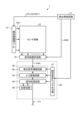
- FIG. 1 is a plan view showing a detection device according to an embodiment.
- FIG. 2 is a block diagram illustrating an example of the configuration of the detection device according to the embodiment.
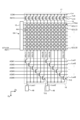
- FIG. 3 is a circuit diagram showing a detection device according to an embodiment.
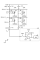
- FIG. 4 is a circuit diagram showing a plurality of pixels.
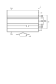
- FIG. 5 is a schematic partial cross-sectional view of the optical sensor according to the embodiment.
- FIG. 6 is a timing waveform diagram showing an example of the operation of the detection device according to the embodiment in one frame period.
- FIG. 7 is a timing waveform diagram showing an example of operation during the reset period in FIG.
- FIG. 8 is a timing waveform diagram showing an example of operation during the readout period in FIG.
- FIG. 1 is a plan view showing a detection device according to an embodiment.
- FIG. 2 is a block diagram illustrating an example of the configuration of the detection device according to the embodiment.
- FIG. 3 is a circuit diagram showing a detection device according to an embodiment.
- FIG. 9 is a timing waveform diagram showing an example of operation during a drive period of one gate line included in the readout period in FIG.
- FIG. 10 is an explanatory diagram for explaining the relationship between driving of the sensor region of the detection device according to the embodiment and the lighting operation of the light source.
- FIG. 11 is a schematic diagram showing a first application example of the detection device according to the embodiment.
- FIG. 12 is a schematic diagram showing a second application example of the detection device according to the embodiment.
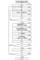
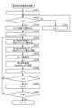
- FIG. 13 is a flowchart illustrating an example of a detection process flow in the detection device according to the embodiment.
- FIG. 14 is a sub-flowchart illustrating an example of the raw data acquisition process.
- FIG. 15 is a diagram showing detection values for F frames at each pixel in the detection area.
- FIG. 16 is a sub-flowchart illustrating an example of the first image generating process.
- FIG. 17 is a sub-flowchart illustrating an example of the first signal intensity extraction process.
- FIG. 18 is a diagram illustrating an example of the time domain data.
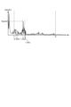
- FIG. 19 is a diagram illustrating an example of frequency domain data.
- FIG. 20 is a sub-flowchart showing an example of the binarization process in the first image generation process.
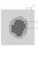
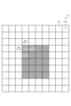
- FIG. 21 is a diagram showing a specific example of an image in which the first binary value for each pixel is visualized.
- FIG. 22 is a sub-flowchart illustrating an example of the filter generation process.
- FIG. 23 is a sub-flowchart showing an example of the edge extraction process.
- FIG. 24 is a diagram showing a specific example of an image in which the second binary value for each pixel is visualized.
- FIG. 25 is a sub-flowchart showing an example of the averaging process.
- FIG. 26 is a diagram showing an example of the average value of the signal intensities of a plurality of pixels in the image shown in FIG.
- FIG. 27 is a diagram illustrating an example of the filter value.
- FIG. 28 is a sub-flowchart illustrating an example of the second image generating process.
- FIG. 29 is a sub-flowchart illustrating an example of the second signal strength calculation process.
- FIG. 30 is a diagram illustrating an example of the second frequency domain data.
- FIG. 31 is a schematic diagram showing the positional relationship between the pulse wave component detection region and the body movement noise component detection region in the sensor region.
- FIG. 32 is a sub-flowchart showing an example of the binarization process in the second image generation process.
- FIG. 33 is a diagram showing a specific example of an image in which the third binary value for each pixel is visualized.
- FIG. 34 is a sub-flowchart showing an example of the pulse wave generating process.
- FIG. 35 is a sub-flowchart showing an example of the first pulse wave generating process.
- FIG. 36 is a sub-flowchart showing an example of the second pulse wave generating process.
- FIG. 37 is a diagram showing an example of the first frequency domain data in a case where the time domain data does not contain a periodic noise component such as body movement noise.
- FIG. 38 is a diagram showing an example of the second frequency domain data in a case where the time domain data does not contain a periodic noise component such as body movement noise.
- FIG. 1 is a plan view showing a detection device according to an embodiment.
- detection device 1 is configured as a detection device that is attached to, for example, a finger or wrist of a subject and detects the subject's pulse wave as biometric information.
- the detection device 1 has a sensor substrate 21, a sensor region 10, a gate line driving circuit 15, a signal line selection circuit 16, an AFE (Analog Front End) circuit 48, a control circuit 122, a power supply circuit 123, a first light source 61, and a second light source 62.
- AFE Analog Front End
- the detection device 1 is electrically connected to the host.
- the host is, for example, a higher-level control device of an apparatus (not shown) to which the detection device 1 is applied.
- the detection device 1 according to the first embodiment transmits the acquired biometric information to the host via the output circuit 126.
- the control board 121 is electrically connected to the sensor substrate 21 via a flexible printed circuit board 71.
- the flexible printed circuit board 71 is provided with an AFE circuit 48.
- the control board 121 is provided with a control circuit 122, a power supply circuit 123, and an output circuit 126.
- the control circuit 122 is, for example, a control IC (Control Integrated Circuit) that outputs a logic control signal.
- the control circuit 122 may be, for example, a PLD (Programmable Logic Device) such as an FPGA (Field Programmable Gate Array).
- the control circuit 122 supplies control signals to the sensor region 10, the gate line driving circuit 15, and the signal line selection circuit 16 to control the detection operation of the sensor region 10.
- the control circuit 122 also supplies control signals to the first light source 61 and the second light source 62 to control whether the first light source 61 and the second light source 62 are turned on or off.
- the power supply circuit 123 supplies voltage signals such as the sensor power supply potential VDDSNS (see FIG. 4) to the sensor region 10, the gate line driving circuit 15, and the signal line selection circuit 16.
- the power supply circuit 123 also supplies a power supply voltage to the first light source 61 and the second light source 62.
- the output circuit 126 is, for example, a USB controller IC, and controls communication between the control circuit 122 and the host.
- the sensor substrate 21 has a detection area AA and a peripheral area GA.
- the detection area AA is an area in which the multiple optical sensors PD (see FIG. 4) of the sensor area 10 are arranged in a matrix.
- the peripheral area GA is an area between the outer periphery of the detection area AA and the end of the sensor substrate 21, where no optical sensors PD are provided.
- the gate line driving circuit 15 and the signal line selection circuit 16 are provided in the peripheral area GA. Specifically, the gate line driving circuit 15 is provided in a region of the peripheral area GA that extends along the second direction Dy. The signal line selection circuit 16 is provided in a region of the peripheral area GA that extends along the first direction Dx, and is provided between the sensor area 10 and the AFE circuit 48.
- the first direction Dx is a direction in a plane parallel to the sensor substrate 21.
- the second direction Dy is a direction in a plane parallel to the sensor substrate 21, and is a direction perpendicular to the first direction Dx.
- the second direction Dy may intersect the first direction Dx without being perpendicular to it.
- the third direction Dz is a direction perpendicular to the first direction Dx and the second direction Dy, and is a normal direction of the sensor substrate 21.
- the multiple first light sources 61 are provided on the first light source substrate 51 and are arranged along the second direction Dy.
- the multiple second light sources 62 are provided on the second light source substrate 52 and are arranged along the second direction Dy.
- the first light source substrate 51 and the second light source substrate 52 are electrically connected to the control circuit 122 and the power supply circuit 123 via terminal portions 124 and 125, respectively, provided on the control board 121.
- the multiple first light sources 61 and the multiple second light sources 62 may be, for example, inorganic LEDs (Light Emitting Diodes) or organic ELs (OLEDs: Organic Light Emitting Diodes).
- the first light source 61 and the second light source 62 emit at least one of visible light, near-infrared light, and infrared light.
- the first light source 61 and the second light source 62 may emit light of different wavelengths, or may emit light of the same wavelength.
- the first light emitted by the first light source 61 (or the second light source 62) may be red light or infrared light, or may be blue light or green light.
- the first light emitted by the first light source 61 may be red light
- the second light emitted by the second light source 62 may be infrared light.
- the present disclosure is not limited by the emission colors of the first light source 61 and the second light source 62.
- the light emitted from the first light source 61 and the second light source 62 is reflected by or transmitted through the surface or interior of, for example, the subject's finger or wrist, and enters the sensor area 10. This allows the sensor area 10 to detect the subject's pulse wave.
- FIG. 2 is a block diagram showing an example of the configuration of a detection device according to an embodiment. As shown in FIG. 2, the detection device 1 further includes a detection control circuit 11 and a detection circuit 40.
- the sensor region 10 has multiple optical sensors PD.
- the optical sensors PD of the sensor region 10 are organic photodiodes (OPDs), and output an electrical signal corresponding to the irradiated light to the signal line selection circuit 16 as a detection signal Vdet.
- OPDs organic photodiodes
- the sensor region 10 also performs detection according to a gate drive signal Vgcl supplied from the gate line drive circuit 15.
- the detection control circuit 11 is a circuit that supplies control signals to the gate line drive circuit 15, the signal line selection circuit 16, and the detection circuit 40, respectively, and controls their operation.
- the detection control circuit 11 supplies various control signals, such as a start signal STV, a clock signal CK, and a reset signal RST1, to the gate line drive circuit 15.
- the detection control circuit 11 also supplies various control signals, such as a selection signal ASW, to the signal line selection circuit 16.
- the detection control circuit 11 also supplies various control signals to the first light source 61 and the second light source 62, and controls the lighting and non-lighting of each.
- the gate line driving circuit 15 is a circuit that drives multiple gate lines GCL (see FIG. 3) based on various control signals.
- the gate line driving circuit 15 selects multiple gate lines GCL sequentially or simultaneously, and supplies a gate driving signal Vgcl to the selected gate lines GCL. In this way, the gate line driving circuit 15 selects multiple photosensors PD connected to the gate lines GCL.
- the signal line selection circuit 16 is a switch circuit that sequentially or simultaneously selects multiple signal lines SGL (see FIG. 3).
- the signal line selection circuit 16 is, for example, a multiplexer.
- the signal line selection circuit 16 electrically connects the selected signal line SGL to the AFE circuit 48 based on a selection signal ASW supplied from the detection control circuit 11. As a result, the signal line selection circuit 16 outputs the detection signal Vdet of the optical sensor PD to the detection circuit 40.
- the detection circuit 40 includes an AFE circuit 48, a signal processing circuit 44, a memory circuit 46, and a detection timing control circuit 47.
- the detection timing control circuit 47 controls the AFE circuit 48 and the signal processing circuit 44 to operate in synchronization based on a control signal supplied from the detection control circuit 11.
- the AFE circuit 48 detects the detection signals of each optical sensor PD output from the sensor area 10 in time series.
- the AFE circuit 48 is, for example, an analog front-end IC.
- the AFE circuit 48 is a signal processing circuit that has at least the functions of the detection signal amplifier circuit 42 and the A/D conversion circuit 43.
- the detection signal amplifier circuit 42 amplifies the detection signal Vdet.
- the A/D conversion circuit 43 converts the analog signal output from the detection signal amplifier circuit 42 into a digital signal at a predetermined sampling period.
- the signal processing circuit 44 and the memory circuit 46 are included in the control circuit 122.
- the signal processing circuit 44 acquires the subject's pulse wave based on the detection values of each optical sensor PD output from the AFE circuit 48.
- the memory circuit 46 temporarily stores the signal processed by the signal processing circuit 44.
- the memory circuit 46 may include, for example, a RAM (Random Access Memory), a ROM (Read Only Memory), an EEPROM (Electrically Erasable Programmable Read Only Memory), etc.
- the memory circuit 46 may also be a register circuit, etc.
- FIG. 3 is a circuit diagram showing a detection device according to an embodiment. As shown in FIG. 3, the sensor area 10 has a plurality of pixels PAA arranged in a planar shape.
- the multiple pixels PAA are arranged, for example, in a matrix in the first direction Dx and the second direction Dy. Without being limited to this, the multiple pixels PAA may be arranged in a staggered pattern in the detection area AA.
- Each of the multiple pixels PAA is provided with a photosensor PD.
- Each photosensor PD outputs an electrical signal (electric potential) according to the light irradiated thereon.
- the gate line GCL extends in the first direction Dx and is connected to a plurality of pixels PAA arranged in the first direction Dx.
- the plurality of gate lines GCL(1), GCL(2), ..., GCL(8) are arranged in the second direction Dy and are each connected to the gate line driving circuit 15.
- gate lines GCL when there is no need to distinguish between the plurality of gate lines GCL(1), GCL(2), ..., GCL(8), they are simply referred to as gate lines GCL.
- the signal line SGL extends in the second direction Dy and is connected to the photosensors PD of the multiple pixels PAA arranged in the second direction Dy.
- the multiple signal lines SGL(1), SGL(2), ..., SGL(12) are arranged in the first direction Dx and are each connected to the signal line selection circuit 16 and the reset circuit 17.
- signal lines SGL when it is not necessary to distinguish between the multiple signal lines SGL(1), SGL(2), ..., SGL(12), they will simply be referred to as signal lines SGL.
- a sensor region 10 is provided between the signal line selection circuit 16 and the reset circuit 17.
- the signal line selection circuit 16 and the reset circuit 17 may each be connected to the ends of the signal lines SGL in the same direction.
- the gate line driving circuit 15 receives various control signals, such as a start signal STV, a clock signal CK, and a reset signal RST1, from the control circuit 122 (see FIG. 1). Based on the various control signals, the gate line driving circuit 15 sequentially selects multiple gate lines GCL(1), GCL(2), ..., GCL(8) in a time-division multiplexing manner. The gate line driving circuit 15 supplies a gate driving signal Vgcl to the selected gate line GCL. As a result, the gate driving signal Vgcl is supplied to multiple first switching elements Tr connected to the gate line GCL, and multiple pixels PAA arranged in the first direction Dx are selected as detection targets.
- various control signals such as a start signal STV, a clock signal CK, and a reset signal RST1
- the signal line selection circuit 16 has a plurality of selection signal lines Lsel, a plurality of output signal lines Lout, and a third switching element TrS.
- the plurality of third switching elements TrS are provided corresponding to the plurality of signal lines SGL, respectively.
- the six signal lines SGL(1), SGL(2), ..., SGL(6) are connected to a common output signal line Lout1.
- the six signal lines SGL(7), SGL(8), ..., SGL(12) are connected to a common output signal line Lout2.
- the output signal lines Lout1, Lout2 are each connected to the AFE circuit 48.
- the signal lines SGL(1), SGL(2), ..., SGL(6) are defined as a first signal line block
- the signal lines SGL(7), SGL(8), ..., SGL(12) are defined as a second signal line block.
- the multiple selection signal lines Lsel are each connected to the gate of the third switching element TrS included in one signal line block. Furthermore, one selection signal line Lsel is connected to the gate of the third switching element TrS of multiple signal line blocks.
- the selection signal lines Lsel1, Lsel2, ..., Lsel6 are connected to the third switching elements TrS corresponding to the signal lines SGL(1), SGL(2), ..., SGL(6), respectively.
- the selection signal line Lsel1 is connected to the third switching element TrS corresponding to the signal line SGL(1) and the third switching element TrS corresponding to the signal line SGL(7).
- the selection signal line Lsel2 is connected to the third switching element TrS corresponding to the signal line SGL(2) and the third switching element TrS corresponding to the signal line SGL(8).
- the control circuit 122 (see FIG. 1) sequentially supplies the selection signal ASW to the selection signal line Lsel.
- the signal line selection circuit 16 sequentially selects the signal lines SGL in one signal line block in a time-division manner through the operation of the third switching element TrS.
- the signal line selection circuit 16 also selects one signal line SGL each in each of the multiple signal line blocks.
- the detection device 1 can reduce the number of ICs (Integrated Circuits) including the AFE circuit 48, or the number of IC terminals.
- the reset circuit 17 has a reference signal line Lvr, a reset signal line Lrst, and a fourth switching element TrR.
- the fourth switching element TrR is provided corresponding to the multiple signal lines SGL.
- the reference signal line Lvr is connected to either the sources or the drains of the multiple fourth switching elements TrR.
- the reset signal line Lrst is connected to the gates of the multiple fourth switching elements TrR.
- the control circuit 122 supplies a reset signal RST2 to the reset signal line Lrst. This turns on the multiple fourth switching elements TrR, and the multiple signal lines SGL are electrically connected to the reference signal line Lvr.
- the power supply circuit 123 supplies a reference signal COM to the reference signal line Lvr. This causes the reference signal COM to be supplied to the capacitive elements Ca (see FIG. 4) included in the multiple pixels PAA.
- FIG. 4 is a circuit diagram showing a plurality of pixels of a detection device according to an embodiment. Note that FIG. 4 also shows the circuit configuration of an AFE circuit 48.
- pixel PAA includes a photosensor PD, a capacitive element Ca, and a first switching element Tr1.
- the capacitive element Ca is a capacitance (sensor capacitance) formed in the photosensor PD, and is equivalently connected in parallel with the photosensor PD.
- the signal line capacitance Cc is a parasitic capacitance formed in the signal line SGL, and is equivalently formed between the signal line SGL and the anode of the photosensor PD and one end of the capacitive element Ca.
- FIG. 4 of the multiple gate lines GCL, two gate lines GCL(m) and GCL(m+1) aligned in the second direction Dy are shown. Also, of the multiple signal lines SGL, two signal lines SGL(n) and SGL(n+1) aligned in the first direction Dx are shown.
- the pixel PAA is the area surrounded by the gate lines GCL and the signal lines SGL.
- the first switching element Tr is provided corresponding to the optical sensor PD.
- the first switching element Tr is composed of a thin film transistor, and in this example, is composed of an n-channel MOS (Metal Oxide Semiconductor) type TFT (Thin Film Transistor).
- MOS Metal Oxide Semiconductor
- TFT Thin Film Transistor
- the gates of the first switching elements Tr belonging to the multiple pixels PAA aligned in the first direction Dx are connected to the gate line GCL.
- the sources of the first switching elements Tr belonging to the multiple pixels PAA aligned in the second direction Dy are connected to the signal line SGL.
- the drains of the first switching elements Tr are connected to the cathodes of the photosensors PD and the capacitive elements Ca.
- the anode of the optical sensor PD is supplied with a sensor power signal (electric potential) VDDSNS from the power supply circuit 123.
- the cathode of the optical sensor PD is supplied with a reference signal COM, which is the initial electric potential of the signal line SGL and the capacitive element Ca, from the power supply circuit 123.
- the switch SSW is turned on during the readout period Pdet (see FIG. 6), and the AFE circuit 48 is connected to the signal line SGL.
- the detection signal amplifier circuit 42 of the AFE circuit 48 converts the current supplied from the signal line SGL into a voltage and amplifies it.
- a reference potential (Vref) having a fixed potential is input to the non-inverting input terminal (+) of the detection signal amplifier circuit 42, and the signal line SGL is connected to the inverting input terminal (-).
- a signal that is the same as the reference signal COM is input as the reference potential (Vref) voltage.
- the detection signal amplifier circuit 42 also has a capacitance element Cb and a reset switch RSW. In the reset period Prst (see FIG. 6), the reset switch RSW is turned on, and the charge of the capacitance element Cb is reset.
- FIG. 5 is a schematic partial cross-sectional view of an optical sensor according to an embodiment.
- the sensor region 10 of the detection device 1 includes a sensor substrate 21, a sensor structure 22, and a protective film 23.
- the sensor substrate 21 is, for example, an insulating substrate formed of a film-like resin.
- the sensor structure 22 has a TFT layer 221, an anode electrode (lower electrode) 222, a photosensor PD, and a cathode electrode (upper electrode) 226.
- the TFT layer 221 is provided with various wiring such as gate lines GCL and signal lines SGL.
- the sensor substrate 21 and the TFT layer 221 form a driving circuit that drives the sensor, and are also called a backplane.
- the optical sensor PD has an active layer 224, an electron transport layer (lower buffer layer) 223 provided between the active layer 224 and an anode electrode (lower electrode) 222, and a hole transport layer (upper buffer layer) 225 provided between the active layer 224 and a cathode electrode (upper electrode) 226.
- the electron transport layer (lower buffer layer) 223, active layer 224, and hole transport layer (upper buffer layer) 225 of the optical sensor PD are stacked in this order in a direction perpendicular to the sensor substrate 21.
- the characteristics (for example, voltage-current characteristics and resistance value) of the active layer 224 change depending on the light irradiated.
- An organic material is used as the material of the active layer 224.
- the active layer 224 is a bulk heterostructure in which a p-type organic semiconductor and an n-type fullerene derivative (PCBM) which is an n-type organic semiconductor are mixed.
- PCBM n-type fullerene derivative
- low molecular weight organic materials such as C 60 (fullerene), PCBM (phenyl C61-butyric acid methyl ester), CuPc (copper phthalocyanine), F 16 CuPc (fluorinated copper phthalocyanine), rubrene (5,6,11,12-tetraphenyltetracene), and PDI (perylene derivative) can be used as the active layer 224.
- C 60 fulllerene
- PCBM phenyl C61-butyric acid methyl ester
- CuPc copper phthalocyanine
- F 16 CuPc fluorinated copper phthalocyanine
- rubrene 5,6,11,12-tetraphenyltetracene
- PDI perylene derivative
- the active layer 224 can be formed by a deposition type (dry process) using these low molecular weight organic materials.
- the active layer 224 may be, for example, a laminated film of CuPc and F 16 CuPc, or a laminated film of rubrene and C 60.
- the active layer 224 can also be formed by a coating type (wet process).
- the active layer 224 is made of a material that combines the above-mentioned low molecular weight organic material and a polymer organic material.
- the polymer organic material for example, P3HT (poly(3-hexylthiophene)), F8BT (F8-alt-benzothiadiazole), etc. can be used.
- the active layer 224 can be a film in a state where P3HT and PCBM are mixed, or a film in a state where F8BT and PDI are mixed.
- the electron transport layer (lower buffer layer) 223 and the hole transport layer (upper buffer layer) 225 are provided to facilitate the electrons and holes generated in the active layer 224 reaching the anode electrode (lower electrode) 222 or the cathode electrode (upper electrode) 226.
- the electron transport layer (lower buffer layer) 223 is in direct contact with the anode electrode (lower electrode) 222.
- the active layer 224 is in direct contact with the electron transport layer (lower buffer layer) 223.
- the material used for the electron transport layer (lower buffer layer) 223 is ethoxylated polyethyleneimine (PEIE).
- the hole transport layer (upper buffer layer) 225 is in direct contact with the active layer 224, and the cathode electrode (upper electrode) 226 is in direct contact with the hole transport layer (upper buffer layer) 225.
- the hole transport layer (upper buffer layer) 225 is a metal oxide layer. Tungsten oxide (WO 3 ), molybdenum oxide, or the like is used as the metal oxide layer.
- the materials and manufacturing methods of the electron transport layer (lower buffer layer) 223, the active layer 224, and the hole transport layer (upper buffer layer) 225 are merely examples, and other materials and manufacturing methods may be used.
- the anode electrode (lower electrode) 222 and the cathode electrode (upper electrode) 226 face each other with the photosensor PD in between.
- the cathode electrode (upper electrode) 226 is made of a conductive material having translucency, such as ITO (Indium Tin Oxide).
- the anode electrode (lower electrode) 222 is made of a metal material, such as silver (Ag) or aluminum (Al). Alternatively, the anode electrode (lower electrode) 222 may be an alloy material containing at least one of these metal materials.
- the anode electrode (lower electrode) 222 can be formed as a semi-transparent electrode having light transmittance.
- the anode electrode (lower electrode) 222 is formed from a thin Ag film having a film thickness of 10 nm, and has a light transmittance of about 60%.
- the optical sensor PD can detect, for example, the first light LD irradiated from the first surface FD side.
- the protective film 23 is provided on the second surface FU, covering the cathode electrode (upper electrode) 226.
- the protective film 23 is a passivation film, and is provided to protect the photosensor PD.
- the reference signal COM that is the initial potential of the signal line SGL and the capacitance element Ca is supplied from the power supply circuit 123 to the cathode of the photosensor PD
- the sensor power supply signal VDDSNS is supplied from the power supply circuit 123 to the cathode of the photosensor PD
- the reference signal COM that is the initial potential of the signal line SGL and the capacitance element Ca is supplied from the power supply circuit 123 to the anode of the photosensor PD.
- the photosensor PD has an active layer 224, a hole transport layer (lower buffer layer) 223 provided between the active layer 224 and the cathode electrode (lower electrode) 222, and an electron transport layer (upper buffer layer) 225 provided between the active layer 224 and the anode electrode (upper electrode) 226.
- the hole transport layer (lower buffer layer) 223, active layer 224, and electron transport layer (upper buffer layer) 225 of the photosensor PD are stacked in this order in a direction perpendicular to the sensor substrate 21.
- the optical sensor PD is not limited to an organic photodiode (OPD).
- OPD organic photodiode
- the optical sensor PD may be, for example, a silicon photodiode (SiPD).
- FIG. 6 is a timing waveform diagram showing an example of the operation of the detection device according to the embodiment in one frame period.
- FIG. 7 is a timing waveform diagram showing an example of the operation of the reset period in FIG. 6.
- FIG. 8 is a timing waveform diagram showing an example of the operation of the readout period in FIG. 6.
- FIG. 9 is a timing waveform diagram showing an example of the operation of the drive period of one gate line included in the row readout period VR in FIG. 6.
- FIG. 10 is an explanatory diagram for explaining the relationship between the drive of the sensor region of the detection device according to the embodiment and the lighting operation of the light source.
- the detection device 1 has a reset period Prst, an exposure period Pex, and a readout period Pdet.
- the power supply circuit 123 supplies a sensor power supply signal VDDSNS to the anode of the photosensor PD throughout the reset period Prst, the exposure period Pex, and the readout period Pdet.
- the sensor power supply signal VDDSNS is a signal that applies a reverse bias between the anode and cathode of the photosensor PD.
- a reference signal COM of substantially 0.75V is applied to the cathode of the photosensor PD, but by applying a sensor power supply signal VDDSNS of substantially -1.25V to the anode, the anode and cathode are reverse biased at substantially 2.0V.
- the control circuit 122 sets the reset signal RST2 to "H” and then supplies a start signal STV and a clock signal CK to the gate line driving circuit 15, starting the reset period Prst.
- the control circuit 122 supplies the reference signal COM to the reset circuit 17 and turns on the fourth switching element TrR for supplying a reset voltage by the reset signal RST2.
- the reference signal COM is supplied to each signal line SGL as a reset voltage.
- the reference signal COM is set to, for example, 0.75 V.
- the gate line driving circuit 15 sequentially selects the gate lines GCL based on the start signal STV, the clock signal CK, and the reset signal RST1.
- the gate line driving circuit 15 sequentially supplies the gate driving signals Vgcl ⁇ Vgcl(1) to Vgcl(M) ⁇ to the gate lines GCL.
- the gate driving signal Vgcl has a pulse-like waveform having a power supply voltage VDD, which is a high-level voltage, and a power supply voltage VSS, which is a low-level voltage.
- the voltage of 0.75 V of the reference signal COM is supplied as the reset voltage.
- the gate line driving circuit 15 supplies a gate driving signal Vgcl(1) of a high-level voltage (power supply voltage VDD) to the gate line GCL(1) during period V(1).
- the control circuit 122 supplies at least one of the selection signals ASW1, ..., ASW6 (selection signal ASW1 in FIG. 7) to the signal line selection circuit 16 during the period when the gate driving signal Vgcl(1) is at a high-level voltage (power supply voltage VDD).
- the signal line SGL of the pixel PAA selected by the selection signal ASW1 is connected to the AFE circuit 48.
- the reset voltage reference signal COM
- the gate line driving circuit 15 supplies high-level voltage gate driving signals Vgcl(2), ..., Vgcl(M-1), Vgcl(M) to the gate lines GCL(2), ..., GCL(M-1), GCL(M), respectively, during periods V(2), ..., V(M-1), V(M).
- the capacitive elements Ca of all pixels PAA are sequentially electrically connected to the signal line SGL and the reference signal COM is supplied. As a result, the capacitance of the capacitive elements Ca is reset. Note that it is also possible to reset the capacitance of some of the capacitive elements Ca of the pixels PAA by partially selecting the gate lines and signal lines SGL.
- Examples of exposure timing include the gate line non-selection exposure control method and the constant exposure control method.
- the gate line non-selection exposure control method the gate drive signals ⁇ Vgcl(1) to (M) ⁇ are sequentially supplied to all gate lines GCL connected to the photosensor PD to be detected, and a reset voltage is supplied to all photosensors PD to be detected. After that, when all gate lines GCL connected to the photosensor PD to be detected are at a low voltage (the first switching element Tr is off), exposure begins, and exposure is performed during the exposure period Pex.
- the gate drive signals ⁇ Vgcl(1) to (M) ⁇ are sequentially supplied to the gate lines GCL connected to the photosensor PD to be detected, and reading is performed during the readout period Pdet.
- the gate drive signal Vgcl(1) is supplied to the gate line GCL during the reset period Prst, and then the exposure period Pex(1) begins.
- the exposure period Pex ⁇ (1)...(M) ⁇ is a substantial exposure period, which is a period during which the capacitance element Ca is charged from the photosensor PD, and does not include periods during which light is irradiated outside of this period.
- the charge charged in the capacitance element Ca during the reset period Prst flows as a reverse current (from the cathode to the anode) to the photosensor PD by light irradiation, and the potential difference between both ends of the capacitance element Ca decreases.
- the substantial exposure periods Pex(1),...,Pex(M) in the pixel PAA corresponding to each gate line GCL have different start and end timings.
- the exposure periods Pex(1),...,Pex(M) are each started at the timing when the gate drive signal Vgcl changes from the high-level voltage power supply voltage VDD to the low-level voltage power supply voltage VSS during the reset period Prst.
- each of the exposure periods Pex(1), ..., Pex(M) ends when the gate drive signal Vgcl changes from the power supply voltage VSS to the power supply voltage VDD during the readout period Pdet.
- the exposure time of each of the exposure periods Pex(1), ..., Pex(M) is equal.
- the control circuit 122 sets the reset signal RST2 to a low-level voltage. This stops the operation of the reset circuit 17.
- the reset signal may be at a high-level voltage only during the reset period Prst.
- the gate line drive circuit 15 sequentially supplies the gate drive signals Vgcl(1), ..., Vgcl(M) to the gate line GCL.
- the gate line driving circuit 15 supplies a gate driving signal Vgcl(1) of a high-level voltage (power supply voltage VDD) to the gate line GCL(1) during the row readout period VR(1).
- the control circuit 122 sequentially supplies selection signals ASW1, ..., ASW6 to the signal line selection circuit 16 during the period when the gate driving signal Vgcl(1) is at a high-level voltage (power supply voltage VDD).
- the signal lines SGL of the pixels PAA selected by the gate driving signal Vgcl(1) are sequentially connected to the AFE circuit 48.
- the detection signal Vdet is supplied to the AFE circuit 48 for each pixel PAA.
- the gate line driving circuit 15 supplies high-level voltage gate driving signals Vgcl(2), ..., Vgcl(M-1), Vgcl(M) to the gate lines GCL(2), ..., GCL(M-1), GCL(M) during the row readout periods VR(2), ..., VR(M-1), VR(M). That is, the gate line driving circuit 15 supplies the gate driving signal Vgcl to the gate line GCL for each row readout period VR(1), VR(2), ..., VR(M-1), VR(M). For each period in which each gate driving signal Vgcl is at a high level voltage, the signal line selection circuit 16 selects the signal lines SGL sequentially or simultaneously based on the selection signal ASW. The signal line selection circuit 16 connects each signal line SGL sequentially or simultaneously to one AFE circuit 48. As a result, during the readout period Pdet, the detection device 1 can output the detection signals Vdet of all pixels PAA to the AFE circuit 48.
- the output (Vout) of the third switching element TrS is reset to a reference potential (Vref) voltage in advance.
- the reference potential (Vref) voltage is a reset voltage, for example, 0.75V.
- the gate drive signal Vgcl(j) goes high, turning on the first switching element Tr of the row, and the signal line SGL of each row becomes a voltage corresponding to the charge stored in the capacitance (capacitive element Ca) of the pixel PAA.
- a period t2 occurs during which the selection signal ASW(k) goes high.
- the selection signal ASW(k) goes high and the third switching element TrS turns on, the AFE circuit 48 and the capacitance (capacitive element Ca) of the pixel PAA are electrically connected via the third switching element TrS. Therefore, the output (Vout) of the third switching element TrS (see FIG. 4) changes to a voltage corresponding to the charge stored in the capacitance (capacitor Ca) of the pixel PAA (period t3). In the example of FIG. 9, this voltage drops from the reset voltage as shown in period t3.
- the switch SSW is turned on (period t4 when the SSW signal is at a high level)
- the charge stored in the capacitance (capacitor Ca) of the pixel PAA moves to the capacitance (capacitor Cb) of the detection signal amplifier circuit 42 of the AFE circuit 48, and the output voltage of the detection signal amplifier circuit 42 becomes a voltage corresponding to the charge stored in the capacitor Cb.
- the inverting input of the detection signal amplifier circuit 42 becomes the imaginary short potential of the operational amplifier, so it becomes the reference potential (Vref).
- the output voltage of the detection signal amplifier circuit 42 is read out by the A/D conversion circuit 43.
- the waveforms of the selection signals ASW(k), ASW(k+1), ... corresponding to the signal lines SGL of each column become high to sequentially turn on the third switching elements TrS, and similar operations are sequentially performed to sequentially read out the charge stored in the capacitance (capacitance element Ca) of the pixel PAA connected to the gate line GCL.
- ASW(k), ASW(k+1), ... in FIG. 9 are, for example, any of ASW1 to ASW6 in FIG. 9.
- the voltage of the capacitor Cb becomes a voltage corresponding to the charge accumulated in the capacitance (capacitor Ca) of pixel PAA at the point where the third switching element TrS is turned on in response to the selection signal ASW (k).
- the output of the detection signal amplifier circuit 42 becomes a voltage corresponding to the capacitance of the capacitor Cb after the output (Vout) of the third switching element TrS becomes the reference potential (Vref) voltage due to an imaginary short.
- the output voltage of the detection signal amplifier circuit 42 is read by the A/D conversion circuit 43.
- the voltage of the capacitance element Cb is, for example, the voltage between two electrodes provided in the capacitor that constitutes the capacitance element Cb.
- the detection device 1 executes the above-mentioned reset period Prst, exposure period Pex ⁇ (1)...(M) ⁇ , and readout period Pdet.
- the gate line driving circuit 15 sequentially scans the gate lines GCL(1) to GCL(M).
- detection in periods t(1), t(2), t(3), and t(4) that is, detection in which the gate lines GCL(1) to GCL(M) are scanned in the reset period Prst and readout period Pdet and the detection signal Vdet is obtained from the signal line SGL of each column, is referred to as detection of one frame.
- the control circuit 122 can control the lighting and non-lighting of the light sources depending on the detection target.
- FIG. 10 shows an example in which the first light source 61 is turned on during periods t(1) and t(3), and the second light source 62 is turned on during periods t(2) and t(4). That is, in the first example shown in FIG. 10, the control circuit 122 alternately switches the first light source 61 and the second light source 62 on and off for each detection of one frame. This is not limited to the above, and for example, the control circuit 122 may switch the lighting and non-lighting of the first light source 61 and the second light source 62 on and off every predetermined period, or may light one of them continuously.
- FIG. 11 is a schematic diagram showing a first application example of the detection device according to the embodiment.
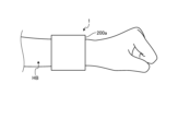
- FIG. 12 is a schematic diagram showing a second application example of the detection device according to the embodiment.
- the detection device 1 is a ring-shaped wearable device 200 that can be attached to and detached from the human body, and is worn on the subject's finger Fg.
- the finger Fg includes the thumb, index finger, middle finger, ring finger, little finger, etc.
- the detection device 1 according to the present disclosure acquires a pulse wave from the finger Fg on which it is worn.
- the detection device 1 is a ring-shaped wearable device 200a such as a smart watch, wristwatch, or wristband, and is worn on the subject's body HB.
- the human body HB includes the subject's wrist, arm, leg, etc.
- the detection device 1 acquires a pulse wave from the human body HB (e.g., the subject's arm) on which it is worn.
- periodic body movement noise caused by human body movements such as walking may be erroneously determined as a pulse wave.
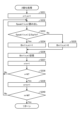
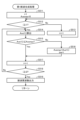
- FIG. 13 is a flowchart showing an example of a detection process flow in a detection device according to an embodiment. Each process shown in FIG. 13 is mainly executed by the signal processing circuit 44 of the detection circuit 40.
- X ⁇ n,m> indicates the variable for pixel PAA in column n and row m.
- the variable X ⁇ n,m> contains the coordinate information of pixel PAA from which the variable X ⁇ n,m> was obtained.
- X(f) ⁇ n,m> indicates the variable X ⁇ n,m> for the fth frame.
- the signal processing circuit 44 executes the raw data acquisition process shown in FIG. 14 to acquire detection values Raw(f) ⁇ n,m> for multiple frames in each pixel PAA of the sensor area 10 (FIG. 13, step S100).
- FIG. 14 is a sub-flowchart showing an example of the raw data acquisition process.
- the number of frames F when acquiring detection values Raw(f) ⁇ n,m> for multiple frames is set to a number that allows multiple pulse wave peaks to be acquired (for example, about 10 times).
- the number of frames F is defined by the following formula (1), where P is the acquisition period for the detection values Raw(f) ⁇ n,m> and t is the sampling period.
- the acquisition period P for the detection values Raw(f) ⁇ n,m> is, for example, 10 sec to 20 sec.
- the number of frames F is stored, for example, in the memory circuit 46.
- FIG. 15 is a diagram showing the detection values for F frames at each pixel in the detection area.
- the detection values Raw(f) ⁇ n,m> for F frames at each pixel PAA are stored in the memory circuit 46.
- FIG. 16 is a sub-flowchart showing an example of the first image generation process.
- FIG. 16 is a sub-flowchart showing an example of the first signal intensity extraction process.
- step S215 the detection value Raw(f) ⁇ n,m> for F frames at pixel PAA in the nth column and mth row is read out.
- FFT Fast Fourier Transform
- FIG. 18 is a diagram showing an example of time domain data.
- the horizontal axis indicates frame f (time)
- the vertical axis indicates the detection value Raw(f) ⁇ n,m> corresponding to each frame f.
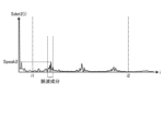
- FIG. 19 is a diagram showing an example of frequency domain data.
- the horizontal axis indicates frequency line i
- the vertical axis indicates signal strength Sdet(i) ⁇ n,m> corresponding to each frequency line i.
- the number I of frequency lines included in the frequency domain data is defined by the following equation (2).
- the signal processing circuit 44 limits the frequency domain data shown in FIG. 19 to a frequency range equal to or greater than the first frequency line i1 and less than the second frequency line i2, stores it in the memory circuit 46 as the first frequency domain data (signal strength Sdet1(i) ⁇ n,m>) (step S217), and extracts a peak value in the first frequency domain data (signal strength Sdet1(i) ⁇ n,m>) (step S218).
- the frequency corresponding to the first frequency line i1 is, for example, 0.5 Hz
- the frequency corresponding to the second frequency line i2 is, for example, 4 Hz.
- the first frequency domain data (signal strength Sdet1(i) ⁇ n,m>) is stored in the memory circuit 46.
- the signal processing circuit 44 stores the peak value extracted in step S218 in the memory circuit 46 as the first signal intensity Peak1 ⁇ n,m> for pixel PAA in the nth column and mth row (step S219).
- the signal component around 0.75 Hz is the body movement component
- the signal component around 1.3 Hz is the pulse wave component.
- the signal strength of the frequency line corresponding to the body movement component is extracted as the first signal strength Peak1 ⁇ n,m>.
- the first frequency domain data (signal intensity Sdet1(i) ⁇ n,m>) and the first signal intensity Peak1 ⁇ n,m> for each pixel PAA are stored in the memory circuit 46.
- FIG. 20 is a sub-flowchart showing an example of the binarization process in the first image generation process.
- the first binary value Bin1 ⁇ n,m> for each pixel PAA is stored in the memory circuit 46.
- the image shown in FIG. 21 is generated.
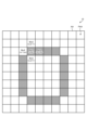
- FIG. 21 is a diagram showing a specific example of an image in which the first binary value for each pixel is visualized.
- FIG. 21 shows an example in which the first binary value Bin1 ⁇ n,m>, the first binary value Bin1 ⁇ n+1,m>, and the first binary value Bin1 ⁇ n,m+1> are "1," and the first binary value Bin1 ⁇ n,m-1> and the first binary value Bin1 ⁇ n-1,m> are "0.”
- the region in the image shown in FIG. 21 where the first binary value Bin1 is “1” is defined as the "first region.”
- the first region indicates the region in the image shown in FIG. 21 where the first signal strength Peak1 ⁇ n,m> is equal to or greater than the threshold value Sig1th.
- FIG. 22 is a sub-flowchart showing an example of the filter generation process.
- FIG. 23 is a sub-flowchart showing an example of edge extraction processing.
- the second binary value Bin2 ⁇ n,m> for each pixel PAA is stored in the memory circuit 46.
- the image shown in FIG. 24 is generated.
- FIG. 24 is a diagram showing a specific example of an image in which the second binary value for each pixel is visualized.
- FIG. 24 shows an example in which the second binary value Bin2 ⁇ n,m> and the second binary value Bin2 ⁇ n+1,m> are "1", and the second binary value Bin2 ⁇ n,m-1>, the second binary value Bin2 ⁇ n-1,m>, and the second binary value Bin2 ⁇ n,m+1> are "0".
- edge extraction process is just one example, and it is also possible to use, for example, a known contour tracing processing algorithm to extract pixels PAA located on the outer periphery of the first region (see FIG. 21).
- FIG. 25 is a sub-flowchart showing an example of the averaging process.
- the signal processing circuit 44 calculates the average value Ave(i) for each frequency line i of the first frequency domain data (signal strength Sdet1(i) ⁇ n,m>) for all pixels PAA included in the area where the second binary value Bin2 is "1" in the image shown in FIG. 24 (step S334).
- the average value Ave(i) for each frequency line i can be expressed by the following formula (3).
- the signal processing circuit 44 performs a threshold determination process on the average value Ave(i) calculated in step S334 to generate a filter value Fil(i) corresponding to the frequency line i. Specifically, the signal processing circuit 44 determines whether the average value Ave(i) calculated in step S334 is equal to or greater than a predetermined threshold value Aveth (step S335).
- the signal processing circuit 44 sets the filter value Fil(i) to "0" and stores it in the memory circuit 46 (step S336). If the average value Ave(i) is less than the threshold value Aveth (step S335; No), the signal processing circuit 44 sets the filter value Fil(i) to "1" and stores it in the memory circuit 46 (step S337).
- the filter value Fil(i) corresponding to the frequency line i where the signal strength Ave(i) after averaging is equal to or greater than the threshold value Aveth is stored in the memory circuit 46 as "0"
- the filter value Fil(i) corresponding to the frequency line i where the signal strength Ave(i) after averaging is less than the threshold value Aveth is stored in the memory circuit 46 as "1".
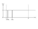
- step S339 When the frequency line i is equal to or greater than the second frequency line i2 (i ⁇ i2) (step S339; Yes), the process returns from the filter generation process shown in FIG. 22 to the detection process flow shown in FIG. 13.
- FIG. 26 is a diagram showing an example of the average value of the signal strength of multiple pixels in the image shown in FIG. 24.
- FIG. 27 is a diagram showing an example of the filter value.
- the horizontal axis indicates the frequency line i.
- the vertical axis shown in FIG. 26 indicates the average value Ave(i) corresponding to each frequency line i.
- the vertical axis shown in FIG. 27 indicates the filter value Fil(i) corresponding to each frequency line i.
- the above-mentioned process causes the filter value Fil of the frequency line where the average value Ave is equal to or greater than the threshold value Aveth to become "0."
- the example shown in Figures 26 and 27 shows an example where the filter value Fil around 0.75 Hz and the filter value Fil around 1.5 Hz are both "0.”
- the process returns from the filter generation process shown in FIG. 22 to the detection process flow shown in FIG. 13, and the second image generation process shown in FIG. 28 is executed (FIG. 13, step S400), and in the second signal strength calculation process shown in FIG. 29 (FIG. 28, step S410), the filter value Fil(i) is applied to the first frequency domain data (signal strength Sdet1(i) ⁇ n,m>). This suppresses the signal strength corresponding to the frequency line where the filter value Fil(i) is "0".
- FIG. 28 is a sub-flowchart showing an example of the second image generation process.
- FIG. 29 is a sub-flowchart showing an example of the second signal intensity calculation process.
- the signal processing circuit 44 reads out the filter value Fil(i) corresponding to the frequency line i from the memory circuit 46 (step S414).
- the second frequency domain data (signal strength Sdet2(i) ⁇ n,m>) can be expressed by the following formula (4).
- FIG. 30 is a diagram showing an example of second frequency domain data.
- the horizontal axis indicates frequency line i
- the vertical axis indicates signal strength Sdet2(i) ⁇ n,m> corresponding to each frequency line i.
- a filter value Fil(i) corresponding to each frequency line i to the first frequency domain data (signal strength Sdet1(i) ⁇ n,m>) for each pixel PAA, second frequency domain data (signal strength Sdet2(i) ⁇ n,m>) in which the signal strength corresponding to the frequency line where the filter value Fil(i) is "0" is suppressed is obtained.
- Second frequency domain data (signal strength Sdet2(i) ⁇ n,m>) in which the body movement component is suppressed is obtained.
- FIG. 31 is a schematic diagram showing the positional relationship between the pulse wave component detection area and the body movement noise component detection area in the sensor area.
- area A1+A2, which includes areas A1 and A2 indicates an area where the binarized value of the signal strength of the frequency component corresponding to body movement noise is "1".
- area A2 excluding area A1 indicates an area where the binarized value of the signal strength of the frequency component corresponding to the pulse wave component is "1".
- area A1 indicates an area where the binarized value of the signal strength of the frequency component corresponding to the pulse wave component is "0".
- the filter value Fil(i) corresponding to the frequency line where the average value Ave(i) of the first frequency domain data (signal strength Sdet1(i) ⁇ n,m>) in the edge portion corresponding to the area A1 is equal to or greater than a predetermined threshold value Aveth is set to "0", and applied to the first frequency domain data (signal strength Sdet1(i) ⁇ n,m>) for each pixel PAA in the entire area (detection area AA) of the sensor area 10 to calculate the second frequency domain data (signal strength Sdet2(i) ⁇ n,m>).
- the second frequency domain data (signal strength Sdet2(i) ⁇ n,m>) in which the body movement component is suppressed.
- the example shown in FIG. 30 shows an example in which the signal components around 0.75 Hz and 1.5 Hz are suppressed as body movement components.
- the signal processing circuit 44 extracts a peak value in the second frequency domain data (signal strength Sdet2(i) ⁇ n,m>) (step S418) and stores the peak value as the second signal strength Peak2 ⁇ n,m> in the memory circuit 46 (step S419).
- the signal component near 1.3 Hz is the pulse wave component.
- the signal strength of the frequency line corresponding to the pulse wave component is extracted as the second signal strength Peak2 ⁇ n,m>.
- the second frequency domain data (signal intensity Sdet2(i) ⁇ n,m>) and the second signal intensity Peak2 ⁇ n,m> for each pixel PAA are stored in the memory circuit 46.
- FIG. 32 is a sub-flowchart showing an example of the binarization process in the second image generation process.
- step S432 By repeating the processes from step S432 to step S440 N ⁇ M times, the third binary value Bin3 ⁇ n,m> for each pixel PAA is stored in the memory circuit 46. By applying the third binary value Bin3 ⁇ n,m> for each pixel PAA to the sensor area 10, the image shown in FIG. 33 is generated.
- FIG. 33 is a diagram showing a specific example of an image in which the third binary value for each pixel is visualized.
- FIG. 33 shows an example in which the third binary value Bin3 ⁇ n,m>, the third binary value Bin3 ⁇ n+1,m>, and the third binary value Bin3 ⁇ n,m+1> are "1", and the third binary value Bin3 ⁇ n,m-1> and the third binary value Bin3 ⁇ n-1,m> are "0".
- the region in the image shown in FIG. 33 where the third binary value Bin3 is "1" is defined as the "second region.”
- the second region indicates the region in the image shown in FIG. 33 where the second signal strength Peak2 ⁇ n,m> is equal to or greater than the threshold value Sig2th.
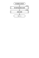
- FIG. 34 is a sub-flowchart showing an example of the pulse wave generation process.
- the signal processing circuit 44 calculates the area S2 of the second region (see FIG. 33) (step S501).
- the area S2 of the second region can be expressed by the following formula (5).
- the signal processing circuit 44 determines whether the area S2 of the second region is less than a predetermined threshold value S2th (S2 ⁇ S2th) (step S502).
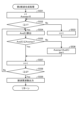
- step S502 If the area S2 of the second region is less than the threshold value S2th (step S502; Yes), the signal processing circuit 44 selects the first frequency domain data (signal strength Sdet1(i) ⁇ n,m>) (step S503) and executes the first pulse wave generation process shown in FIG. 35 (FIG. 34, step S510).
- FIG. 35 is a sub-flowchart showing an example of the first pulse wave generation process.
- the signal processing circuit 44 calculates the average value Ave1(i) for each frequency line i of the first frequency domain data (signal strength Sdet1(i) ⁇ n,m>) for all pixels PAA included in the first domain (see FIG. 21) (step S514).
- the average value Ave1(i) for each frequency line i can be expressed by the following formula (6).
- Ave1(i) ⁇ Sdet1(i) ⁇ n,m>/ ⁇ Bin1 ⁇ n,m>...(6)
- the signal processing circuit 44 executes a process of comparing the average value Ave1(i) calculated in step S514 with Avemax. Specifically, the signal processing circuit 44 determines whether the average value Ave1(i) calculated in step S514 is equal to or less than Avemax (step S515).
- the frequency line ipw corresponding to Avemax which is the peak value of the signal strength Ave1(i) after the averaging process, is stored in the memory circuit 46.
- step S518 When the frequency line i is equal to or greater than the second frequency line i2 (i ⁇ i2) (step S518; Yes), the frequency corresponding to the frequency line ipw is output as the pulse wave frequency to, for example, a host (step S519). Then, the process returns from the pulse wave generation process shown in FIG. 34 to the detection process flow shown in FIG. 13, and the detection process flow ends.
- step S502 if the area S2 of the second region is equal to or greater than the threshold value S2th (step S502; No), the signal processing circuit 44 selects the second frequency domain data (signal strength Sdet2(i) ⁇ n,m>) (step S504) and executes the first pulse wave generation process shown in FIG. 36 (FIG. 34, step S530).
- FIG. 36 is a sub-flowchart showing an example of the second pulse wave generation process.
- the signal processing circuit 44 calculates the average value Ave2(i) for each frequency line i of the second frequency domain data (signal strength Sdet2(i) ⁇ n,m>) for all pixels PAA included in the second domain (see FIG. 33) (step S534).
- the average value Ave2(i) for each frequency line i can be expressed by the following formula (7).
- Ave2(i) ⁇ Sdet2(i) ⁇ n,m>/ ⁇ Bin3 ⁇ n,m>...(7)
- the signal processing circuit 44 executes a process of comparing the average value Ave2(i) calculated in step S534 with Avemax. Specifically, the signal processing circuit 44 determines whether the average value Ave2(i) calculated in step S534 is equal to or less than Avemax (step S535).
- the frequency line ipw corresponding to Avemax which is the peak value of the signal strength Ave2(i) after the averaging process, is stored in the memory circuit 46.
- step S538 When the frequency line i becomes equal to or greater than the second frequency line i2 (i ⁇ i2) (step S538; Yes), the frequency corresponding to the frequency line ipw is output as the pulse wave frequency to, for example, a host (step S539). Then, the process returns from the pulse wave generation process shown in FIG. 34 to the detection process flow shown in FIG. 13, and the detection process flow ends.
- FIG. 37 is a diagram showing an example of first frequency domain data when the time domain data does not include periodic noise components such as body movement noise.
- FIG. 38 is a diagram showing an example of second frequency domain data when the time domain data does not include periodic noise components such as body movement noise.
- the pulse wave component of the first frequency domain data (signal strength Sdet1(i) ⁇ n,m>) is extracted as the first signal strength Peak1 in the first signal strength extraction process ( Figure 16, step S210) shown in Figure 17, and as a result, the second frequency domain data (signal strength Sdet2(i) ⁇ n,m>) in which the pulse wave component is suppressed is obtained in the second signal strength calculation process (Figure 28, step S410) shown in Figure 29.
- step S433 of the binarization process in the second image generation process shown in Figure 32 the number of pixels PAA in which the second signal strength Peak2 ⁇ n,m> is equal to or greater than the threshold value Sig2th (step S433; Yes) is drastically reduced, and as a result, the area S2 of the second region (see Figure 33) is reduced.
- the signal processing circuit 44 selects the first frequency domain data (signal strength Sdet1(i) ⁇ n,m>) (step S503) and executes the first pulse wave generation process shown in FIG. 35 (FIG. 34, step S510). This makes it possible to obtain a highly accurate pulse wave component regardless of the presence or absence of periodic noise components such as body movement noise.
- the above-mentioned processing makes it possible to suppress periodic body movement noise when acquiring biometric information.
- Detection device 10 Sensor region 11 Detection control circuit 15 Gate line driving circuit 16 Signal line selection circuit 21 Sensor substrate 22 Sensor structure 23 Protective film 40 Detection circuit 42 Detection signal amplifier circuit 43 A/D conversion circuit 44 Signal processing circuit 46 Memory circuit 47 Detection timing control circuit 48 AFE circuit 61 First light source (light source) 62 Second light source (light source) 122 Control circuit 123 Power supply circuit 126 Output circuit 200, 200a Wearable device 221 TFT layer 222 Anode electrode (lower electrode) (or cathode electrode (lower electrode)) 223 Electron transport layer (lower buffer layer) (or hole transport layer (lower buffer layer)) 224 Active layer 225 Hole transport layer (upper buffer layer) (or electron transport layer (upper buffer layer)) 226 Cathode electrode (upper electrode) (or anode electrode (upper electrode)) AA Detection area GA Peripheral area GCL Gate line PAA Pixel PD Optical sensor Pdet Readout period
Landscapes
- Health & Medical Sciences (AREA)
- Life Sciences & Earth Sciences (AREA)
- Biomedical Technology (AREA)
- Heart & Thoracic Surgery (AREA)
- Physiology (AREA)
- Biophysics (AREA)
- Pathology (AREA)
- Engineering & Computer Science (AREA)
- Cardiology (AREA)
- Physics & Mathematics (AREA)
- Medical Informatics (AREA)
- Molecular Biology (AREA)
- Surgery (AREA)
- Animal Behavior & Ethology (AREA)
- General Health & Medical Sciences (AREA)
- Public Health (AREA)
- Veterinary Medicine (AREA)
- Solid State Image Pick-Up Elements (AREA)
Abstract
生体情報を取得する際の周期的な体動ノイズを抑制することができる検出装置及びウェアラブルデバイスを提供する。時系列で取得した複数の画素ごとの検出値に基づき画素ごとの第1周波数領域データを生成する。第1周波数領域データの各周波数に対応する信号強度のうちの最大強度を画素ごとの第1信号強度とする。センサ領域内において第1信号強度が所定値以上となる領域を第1領域とする。第1領域の外周部の画素における第1周波数領域データに基づき、第1領域の全ての画素における第1周波数領域データの所定の周波数範囲をマスクした第2周波数領域データを生成する。第2周波数領域データの各周波数に対応する信号強度のうちの最大強度を画素ごとの第2信号強度とする。第2信号強度が所定値以上となる第2領域の面積が所定値以上である場合に、第2周波数領域データに基づき生体情報を取得する。第2領域の面積が所定値未満である場合に、第1周波数領域データに基づき生体情報を取得する。
Description
本発明は、検出装置及びウェアラブルデバイスに関する。
特許文献1には、フォトダイオード等の光電変換素子が半導体基板上に複数配列された光学式センサが記載されている。光学式センサは、照射される光量に応じて光電変換素子から出力される信号が変化することで、生体情報を検出できる。
検出装置を人体に装着して脈波を取得する際、歩行等の人体の運動によって生じる周期的な体動ノイズを脈波として誤判別する場合がある。
本開示は、生体情報を取得する際の周期的な体動ノイズを抑制することができる検出装置及びウェアラブルデバイスを提供することを目的とする。
本開示の一態様に係る検出装置は、面状に配置された複数の画素を有するセンサ領域と、前記センサ領域に光を照射する光源と、前記センサ領域から取得されるデータに基づき、周期的に変動する被験者の生体情報を取得する検出回路と、を備え、前記検出回路は、時系列で取得した複数の前記画素ごとの検出値を、それぞれ周波数ごとの信号強度に変換して、前記画素ごとの第1周波数領域データを生成し、前記第1周波数領域データの各周波数に対応する信号強度のうちの最大強度を画素ごとの第1信号強度とし、前記センサ領域内において、前記第1信号強度が所定値以上となる領域を第1領域とし、前記第1領域の外周部の画素における第1周波数領域データに基づき、前記第1領域の全ての画素における第1周波数領域データの所定の周波数範囲をマスクした第2周波数領域データを生成し、前記第2周波数領域データの各周波数に対応する信号強度のうちの最大強度を画素ごとの第2信号強度とし、前記センサ領域内において、前記第2信号強度が所定値以上となる領域を第2領域とし、前記第2領域の面積が所定値以上である場合に、前記第2周波数領域データに基づき生体情報を取得し、前記第2領域の面積が所定値未満である場合に、前記第1周波数領域データに基づき生体情報を取得する。
本開示の一態様に係るウェアラブルデバイスは、上記検出装置を備え、人体に着脱可能なリング型の形状を有する。
本発明を実施するための形態(実施形態)につき、図面を参照しつつ詳細に説明する。なお、以下の実施形態に記載した内容により本発明が限定されるものではない。また、以下に記載した構成要素には、当業者が容易に想定できるもの、実質的に同一のものが含まれる。さらに、以下に記載した構成要素は適宜組み合わせることが可能である。また、開示はあくまで一例にすぎず、当業者において、発明の主旨を保っての適宜変更について容易に想到し得るものについては、当然に本発明の範囲に含有されるものである。また、図面は説明をより明確にするため、実際の態様に比べ、各部の幅、厚さ、形状等について模式的に表される場合があるが、あくまで一例であって、本発明の解釈を限定するものではない。また、本明細書と各図において、既出の図に関して前述したものと同様の要素には、同一の符号を付して、詳細な説明を適宜省略することがある。
図1は、実施形態に係る検出装置を示す平面図である。本開示において、検出装置1は、例えば被験者の指や手首等に装着され、生体情報として被験者の脈波を検出する検出装置として構成される。
図1に示すように、検出装置1は、センサ基材21と、センサ領域10と、ゲート線駆動回路15と、信号線選択回路16と、AFE(Analog Front End)回路48と、制御回路122と、電源回路123と、第1光源61及び第2光源62と、を有する。
検出装置1は、ホストと電気的に接続される。ホストは、例えば検出装置1が適用される機器(不図示)の上位制御装置である。実施形態1に係る検出装置1は、取得した生体情報を、出力回路126を介してホストに送信する。
センサ基材21には、フレキシブルプリント基板71を介して制御基板121が電気的に接続される。フレキシブルプリント基板71には、AFE回路48が設けられている。制御基板121には、制御回路122、電源回路123、及び出力回路126が設けられている。
制御回路122は、例えばロジック制御信号を出力する制御IC(Control Integrated Circuit)である。制御回路122は、例えばFPGA(Field Programmable Gate Array)等のPLD(Programmable Logic Device)であっても良い。
制御回路122は、センサ領域10、ゲート線駆動回路15及び信号線選択回路16に制御信号を供給して、センサ領域10の検出動作を制御する。また、制御回路122は、第1光源61及び第2光源62に制御信号を供給して、第1光源61及び第2光源62の点灯又は非点灯を制御する。
電源回路123は、センサ電源電位VDDSNS(図4参照)等の電圧信号をセンサ領域10、ゲート線駆動回路15及び信号線選択回路16に供給する。また、電源回路123は、電源電圧を第1光源61及び第2光源62に供給する。
出力回路126は、例えばUSBコントローラICであり、制御回路122とホストとの間の通信制御を行う。
センサ基材21は、検出領域AAと、周辺領域GAとを有する。検出領域AAは、センサ領域10が有する複数の光センサPD(図4参照)が行列状に設けられた領域である。周辺領域GAは、検出領域AAの外周と、センサ基材21の端部との間の領域であり、光センサPDが設けられない領域である。
ゲート線駆動回路15及び信号線選択回路16は、周辺領域GAに設けられる。具体的には、ゲート線駆動回路15は、周辺領域GAのうち第2方向Dyに沿って延在する領域に設けられる。信号線選択回路16は、周辺領域GAのうち第1方向Dxに沿って延在する領域に設けられ、センサ領域10とAFE回路48との間に設けられる。
なお、第1方向Dxは、センサ基材21と平行な面内の一方向である。第2方向Dyは、センサ基材21と平行な面内の一方向であり、第1方向Dxと直交する方向である。なお、第2方向Dyは、第1方向Dxと直交しないで交差してもよい。また、第3方向Dzは、第1方向Dx及び第2方向Dyと直交する方向であり、センサ基材21の法線方向である。
複数の第1光源61は、第1光源基材51に設けられ、第2方向Dyに沿って配列される。複数の第2光源62は、第2光源基材52に設けられ、第2方向Dyに沿って配列される。第1光源基材51及び第2光源基材52は、それぞれ、制御基板121に設けられた端子部124、125を介して、制御回路122及び電源回路123と電気的に接続される。
複数の第1光源61及び複数の第2光源62は、例えば、無機LED(Light Emitting Diode)や、有機EL(OLED:Organic Light Emitting Diode)等が用いられる。
第1光源61及び第2光源62は、可視光、近赤外光、赤外光のうちの少なくとも1つを出射する。第1光源61及び第2光源62は、それぞれ異なる波長の光を出射する態様であっても良いし、同一波長の光を出射する態様であっても良い。具体的には、例えば、少なくとも第1光源61(又は第2光源62)を有する構成において、第1光源61(又は第2光源62)が出射する第1光は、赤色光又は赤外光であっても良いし、青色光又は緑色光であっても良い。あるいは、例えば、第1光源61及び第2光源62を有する構成において、第1光源61が出射する第1光が赤色光であり、第2光源62が出射する第2光が赤外光であっても良い。第1光源61及び第2光源62の発光色により本開示が限定されるものではない。
本開示において、第1光源61及び第2光源62から出射された光は、例えば、被験者の指や手首等の表面あるいは内部で反射又は透過してセンサ領域10に入射する。これにより、センサ領域10は、被験者の脈波を検出することができる。
図2は、実施形態に係る検出装置の構成例を示すブロック図である。図2に示すように、検出装置1は、さらに検出制御回路11と検出回路40と、有する。
センサ領域10は、複数の光センサPDを有する。センサ領域10が有する光センサPDは有機フォトダイオード(OPD:Organic Photodiode)であり、照射される光に応じた電気信号を、検出信号Vdetとして信号線選択回路16に出力する。また、センサ領域10は、ゲート線駆動回路15から供給されるゲート駆動信号Vgclにしたがって検出を行う。
検出制御回路11は、ゲート線駆動回路15、信号線選択回路16及び検出回路40にそれぞれ制御信号を供給し、これらの動作を制御する回路である。検出制御回路11は、スタート信号STV、クロック信号CK、リセット信号RST1等の各種制御信号をゲート線駆動回路15に供給する。また、検出制御回路11は、選択信号ASW等の各種制御信号を信号線選択回路16に供給する。また、検出制御回路11は、各種制御信号を第1光源61及び第2光源62に供給して、それぞれの点灯及び非点灯を制御する。
ゲート線駆動回路15は、各種制御信号に基づいて複数のゲート線GCL(図3参照)を駆動する回路である。ゲート線駆動回路15は、複数のゲート線GCLを順次又は同時に選択し、選択されたゲート線GCLにゲート駆動信号Vgclを供給する。これにより、ゲート線駆動回路15は、ゲート線GCLに接続された複数の光センサPDを選択する。
信号線選択回路16は、複数の信号線SGL(図3参照)を順次又は同時に選択するスイッチ回路である。信号線選択回路16は、例えばマルチプレクサである。信号線選択回路16は、検出制御回路11から供給される選択信号ASWに基づいて、選択された信号線SGLとAFE回路48とを電気的に接続する。これにより、信号線選択回路16は、光センサPDの検出信号Vdetを検出回路40に出力する。
検出回路40は、AFE回路48と、信号処理回路44と、記憶回路46と、検出タイミング制御回路47と、を備える。検出タイミング制御回路47は、検出制御回路11から供給される制御信号に基づいて、AFE回路48と、信号処理回路44と、が同期して動作するように制御する。
AFE回路48は、センサ領域10から出力される各光センサPDの検出信号を時系列で検出する。AFE回路48は、例えばアナログフロントエンドICである。
AFE回路48は、少なくとも検出信号増幅回路42及びA/D変換回路43の機能を有する信号処理回路である。検出信号増幅回路42は、検出信号Vdetを増幅する。A/D変換回路43は、検出信号増幅回路42から出力されるアナログ信号を所定のサンプリング周期でデジタル信号に変換する。
本開示において、信号処理回路44及び記憶回路46は、制御回路122に含まれる。
信号処理回路44は、AFE回路48から出力される各光センサPDの検出値に基づき、被験者の脈波を取得する。
記憶回路46は、信号処理回路44で処理された信号を一時的に保存する。記憶回路46は、例えばRAM(Random Access Memory)、ROM(Read Only Memory)、EEPROM(Electrically Erasable Programmable Read Only Memory)等を含む態様であっても良い。また、記憶回路46は、レジスタ回路等であっても良い。
次に、検出装置1の回路構成例について説明する。図3は、実施形態に係る検出装置を示す回路図である。図3に示すように、センサ領域10は、面状に配置された複数の画素PAAを有する。
具体的に、複数の画素PAAは、例えば、第1方向Dx及び第2方向Dyに並びマトリクス状に配列される。これに限定されず、複数の画素PAAは、検出領域AAにおいて千鳥配置される態様であっても良い。
複数の画素PAAには、それぞれ光センサPDが設けられている。光センサPDは、それぞれに照射される光に応じた電気信号(電位)を出力する。
ゲート線GCLは、第1方向Dxに延在し、第1方向Dxに配列された複数の画素PAAと接続される。また、複数のゲート線GCL(1)、GCL(2)、…、GCL(8)は、第2方向Dyに配列され、それぞれゲート線駆動回路15に接続される。なお、以下の説明において、複数のゲート線GCL(1)、GCL(2)、…、GCL(8)を区別して説明する必要がない場合には、単にゲート線GCLと表す。また、図3では説明を分かりやすくするために、8本のゲート線GCLを示しているが、あくまで一例であり、ゲート線GCLは、M本(Mは自然数、例えばM=256)配列されていてもよい。
信号線SGLは、第2方向Dyに延在し、第2方向Dyに配列された複数の画素PAAの光センサPDに接続される。また、複数の信号線SGL(1)、SGL(2)、…、SGL(12)は、第1方向Dxに配列されて、それぞれ信号線選択回路16及びリセット回路17に接続される。なお、以下の説明において、複数の信号線SGL(1)、SGL(2)、…、SGL(12)を区別して説明する必要がない場合には、単に信号線SGLと表す。
また、説明を分かりやすくするために、12本の信号線SGLを示しているが、あくまで一例であり、信号線SGLは、N本(Nは自然数、例えばN=252)配列されていてもよい。また、図3では、信号線選択回路16とリセット回路17との間にセンサ領域10が設けられている。これに限定されず、信号線選択回路16とリセット回路17とは、信号線SGLの同じ方向の端部にそれぞれ接続されていてもよい。
ゲート線駆動回路15は、スタート信号STV、クロック信号CK、リセット信号RST1等の各種制御信号を、制御回路122(図1参照)から受け取る。ゲート線駆動回路15は、各種制御信号に基づいて、複数のゲート線GCL(1)、GCL(2)、…、GCL(8)を時分割的に順次選択する。ゲート線駆動回路15は、選択されたゲート線GCLにゲート駆動信号Vgclを供給する。これにより、ゲート線GCLに接続された複数の第1スイッチング素子Trにゲート駆動信号Vgclが供給され、第1方向Dxに配列された複数の画素PAAが、検出対象として選択される。
信号線選択回路16は、複数の選択信号線Lselと、複数の出力信号線Loutと、第3スイッチング素子TrSと、を有する。複数の第3スイッチング素子TrSは、それぞれ複数の信号線SGLに対応して設けられている。6本の信号線SGL(1)、SGL(2)、…、SGL(6)は、共通の出力信号線Lout1に接続される。6本の信号線SGL(7)、SGL(8)、…、SGL(12)は、共通の出力信号線Lout2に接続される。出力信号線Lout1、Lout2は、それぞれAFE回路48に接続される。
ここで、信号線SGL(1)、SGL(2)、…、SGL(6)を第1信号線ブロックとし、信号線SGL(7)、SGL(8)、…、SGL(12)を第2信号線ブロックとする。複数の選択信号線Lselは、1つの信号線ブロックに含まれる第3スイッチング素子TrSのゲートにそれぞれ接続される。また、1本の選択信号線Lselは、複数の信号線ブロックの第3スイッチング素子TrSのゲートに接続される。
具体的には、選択信号線Lsel1、Lsel2、…、Lsel6は、それぞれ信号線SGL(1)、SGL(2)、…、SGL(6)に対応する第3スイッチング素子TrSと接続される。また、選択信号線Lsel1は、信号線SGL(1)に対応する第3スイッチング素子TrSと、信号線SGL(7)に対応する第3スイッチング素子TrSと、に接続される。選択信号線Lsel2は、信号線SGL(2)に対応する第3スイッチング素子TrSと、信号線SGL(8)に対応する第3スイッチング素子TrSと、に接続される。
制御回路122(図1参照)は、選択信号ASWを順次選択信号線Lselに供給する。これにより、信号線選択回路16は、第3スイッチング素子TrSの動作により、1つの信号線ブロックにおいて信号線SGLを時分割的に順次選択する。また、信号線選択回路16は、複数の信号線ブロックでそれぞれ1本ずつ信号線SGLを選択する。このような構成により、検出装置1は、AFE回路48を含むIC(Integrated Circuit)の数、又はICの端子数を少なくすることができる。
図3に示すように、リセット回路17は、基準信号線Lvr、リセット信号線Lrst及び第4スイッチング素子TrRを有する。第4スイッチング素子TrRは、複数の信号線SGLに対応して設けられている。基準信号線Lvrは、複数の第4スイッチング素子TrRのソース又はドレインの一方に接続される。リセット信号線Lrstは、複数の第4スイッチング素子TrRのゲートに接続される。
制御回路122は、リセット信号RST2をリセット信号線Lrstに供給する。これにより、複数の第4スイッチング素子TrRがオンになり、複数の信号線SGLは基準信号線Lvrと電気的に接続される。電源回路123は、基準信号COMを基準信号線Lvrに供給する。これにより、複数の画素PAAに含まれる容量素子Ca(図4参照)に基準信号COMが供給される。
図4は、実施形態に係る検出装置の複数の画素を示す回路図である。なお、図4では、AFE回路48の回路構成も併せて示している。図4に示すように、画素PAAは、光センサPDと、容量素子Caと、第1スイッチング素子Tr1とを含む。容量素子Caは、光センサPDに形成される容量(センサ容量)であり、等価的に光センサPDと並列に接続される。さらに、信号線容量Ccは、信号線SGLに形成される寄生容量であり、等価的に、信号線SGLと、光センサPDのアノード及び容量素子Caの一端側との間に形成される。
図4では、複数のゲート線GCLのうち、第2方向Dyに並ぶ2つのゲート線GCL(m)、GCL(m+1)を示す。また、複数の信号線SGLのうち、第1方向Dxに並ぶ2つの信号線SGL(n)、SGL(n+1)を示す。画素PAAは、ゲート線GCLと信号線SGLとで囲まれた領域である。
第1スイッチング素子Trは、光センサPDに対応して設けられる。第1スイッチング素子Trは、薄膜トランジスタにより構成されるものであり、この例では、nチャネルのMOS(Metal Oxide Semiconductor)型のTFT(Thin Film Transistor)で構成されている。
第1方向Dxに並ぶ複数の画素PAAに属する第1スイッチング素子Trのゲートは、ゲート線GCLに接続される。第2方向Dyに並ぶ複数の画素PAAに属する第1スイッチング素子Trのソースは、信号線SGLに接続される。第1スイッチング素子Trのドレインは、光センサPDのカソード及び容量素子Caに接続される。
光センサPDのアノードには、電源回路123からセンサ電源信号(電位)VDDSNSが供給される。また、光センサPDのカソードには、電源回路123から、信号線SGL及び容量素子Caの初期電位となる基準信号COMが供給される。
画素PAAに光が照射されると、光センサPDには光量に応じた電流が流れ、これにより容量素子Caには光量に応じた電荷が蓄積される。第1スイッチング素子Trがオンになると、容量素子Caに蓄積された電荷に応じて、信号線SGLに電流が流れる。信号線SGLは、信号線選択回路16の第3スイッチング素子TrSを介してAFE回路48に接続される。これにより、検出装置1は、画素PAAごとに光センサPDに照射される光の光量に応じた信号を検出できる。
AFE回路48は、読み出し期間Pdet(図6参照)にスイッチSSWがオンになり、信号線SGLと接続される。AFE回路48の検出信号増幅回路42は、信号線SGLから供給された電流を電圧に変換して増幅する。検出信号増幅回路42の非反転入力部(+)には、固定された電位を有する基準電位(Vref)が入力され、反転入力端子(-)には、信号線SGLが接続される。実施形態では、基準電位(Vref)電圧として基準信号COMと同じ信号が入力される。また、検出信号増幅回路42は、容量素子Cb及びリセットスイッチRSWを有する。リセット期間Prst(図6参照)において、リセットスイッチRSWがオンになり、容量素子Cbの電荷がリセットされる。
次に、光センサPDの構成について説明する。図5は、実施形態に係る光センサの模式的な部分断面図である。検出装置1のセンサ領域10は、センサ基材21と、センサ構造体22と、保護膜23と、を備える。センサ基材21は、例えば、フィルム状の樹脂で形成された絶縁性の基材である。
センサ構造体22は、TFT層221と、アノード電極(下部電極)222と、光センサPDと、カソード電極(上部電極)226と、を有する。
TFT層221には、ゲート線GCL、信号線SGL等の各種配線が設けられる。センサ基材21及びTFT層221は、センサを駆動する駆動回路であり、バックプレーンとも呼ばれる。
光センサPDは、活性層224と、活性層224とアノード電極(下部電極)222との間に設けられた電子輸送層(下側バッファ層)223と、活性層224とカソード電極(上部電極)226との間に設けられた正孔輸送層(上側バッファ層)225と、を有する。言い換えると、光センサPDの電子輸送層(下側バッファ層)223、活性層224、正孔輸送層(上側バッファ層)225は、センサ基材21に垂直な方向で、この順で積層される。
活性層224は、照射される光に応じて特性(例えば、電圧電流特性や抵抗値)が変化する。活性層224の材料として、有機材料が用いられる。具体的には、活性層224は、p型有機半導体と、n型有機半導体であるn型フラーレン誘導体(PCBM)とが混在するバルクヘテロ構造である。活性層224として、例えば、低分子有機材料であるC60(フラーレン)、PCBM(フェニルC61酪酸メチルエステル:Phenyl C61-butyric acid methyl ester)、CuPc(銅フタロシアニン:Copper Phthalocyanine)、F16CuPc(フッ素化銅フタロシアニン)、rubrene(ルブレン:5,6,11,12-tetraphenyltetracene)、PDI(Perylene(ペリレン)の誘導体)等を用いることができる。
活性層224は、これらの低分子有機材料を用いて蒸着型(Dry Process)で形成することができる。この場合、活性層224は、例えば、CuPcとF16CuPcとの積層膜、又はrubreneとC60との積層膜であってもよい。活性層224は、塗布型(Wet Process)で形成することもできる。この場合、活性層224は、上述した低分子有機材料と高分子有機材料とを組み合わせた材料が用いられる。高分子有機材料として、例えばP3HT(poly(3-hexylthiophene))、F8BT(F8-alt-benzothiadiazole)等を用いることができる。活性層224は、P3HTとPCBMとが混合した状態の膜、又はF8BTとPDIとが混合した状態の膜とすることができる。
電子輸送層(下側バッファ層)223及び正孔輸送層(上側バッファ層)225は、活性層224で発生した電子及び正孔がアノード電極(下部電極)222又はカソード電極(上部電極)226に到達しやすくするために設けられる。電子輸送層(下側バッファ層)223は、アノード電極(下部電極)222の上に直接、接する。活性層224は、電子輸送層(下側バッファ層)223の上に直接、接する。電子輸送層(下側バッファ層)223の材料は、エトキシ化ポリエチレンイミン(PEIE)が用いられる。
正孔輸送層(上側バッファ層)225は、活性層224の上に直接、接し、カソード電極(上部電極)226は、正孔輸送層(上側バッファ層)225の上に直接、接する。正孔輸送層(上側バッファ層)225は、酸化金属層とされる。酸化金属層として、酸化タングステン(WO3)、酸化モリブデン等が用いられる。
なお、電子輸送層(下側バッファ層)223、活性層224及び正孔輸送層(上側バッファ層)225の材料、製法はあくまで一例であり、他の材料、製法であってもよい。
アノード電極(下部電極)222と、カソード電極(上部電極)226とは、光センサPDを挟んで対向する。カソード電極(上部電極)226は、例えば、ITO(Indium Tin Oxide)等の透光性を有する導電性材料が用いられる。アノード電極(下部電極)222は、例えば、銀(Ag)やアルミニウム(Al)等の金属材料が用いられる。又は、アノード電極(下部電極)222は、これらの金属材料の少なくとも1以上を含む合金材料であってもよい。
アノード電極(下部電極)222の膜厚を制御することで、透光性を有する半透過型電極としてアノード電極(下部電極)222を形成できる。例えば、アノード電極(下部電極)222は、膜厚10nmのAg薄膜で形成することで、60%程度の透光性を有する。この場合、光センサPDは、例えば第1面FD側から照射される第1光LDを検出できる。
保護膜23は、カソード電極(上部電極)226を覆って第2面FUに設けられる。保護膜23は、パッシベーション膜であり、光センサPDを保護するために設けられている。
なお、図4では、光センサPDのアノードに電源回路123からセンサ電源信号VDDSNSが供給され、光センサPDのカソードに電源回路123から信号線SGL及び容量素子Caの初期電位となる基準信号COMが供給される構成を例示したが、例えば、光センサPDのカソードに電源回路123からセンサ電源信号VDDSNSが供給され、光センサPDのアノードに電源回路123から信号線SGL及び容量素子Caの初期電位となる基準信号COMが供給される構成であっても良い。この場合、上述した構成とは異なり、光センサPDは、活性層224と、活性層224とカソード電極(下部電極)222との間に設けられた正孔輸送層(下側バッファ層)223と、活性層224とアノード電極(上部電極)226との間に設けられた電子輸送層(上側バッファ層)225と、を有する。言い換えると、光センサPDの正孔輸送層(下側バッファ層)223、活性層224、電子輸送層(上側バッファ層)225は、センサ基材21に垂直な方向で、この順で積層される。
また、本開示において、光センサPDは有機フォトダイオード(OPD)に限定されない。光センサPDは、例えばシリコンフォトダイオード(SiPD)であっても良い。
次に、検出装置1の動作例について説明する。図6は、実施形態に係る検出装置の1フレーム期間における動作例を表すタイミング波形図である。図7は、図6におけるリセット期間の動作例を表すタイミング波形図である。図8は、図6における読み出し期間の動作例を表すタイミング波形図である。図9は、図6における行読み出し期間VRに含まれる1つのゲート線の駆動期間の動作例を表すタイミング波形図である。図10は、実施形態に係る検出装置のセンサ領域の駆動と、光源の点灯動作との関係を説明するための説明図である。
図6に示すように、検出装置1は、リセット期間Prst、露光期間Pex及び読み出し期間Pdetを有する。電源回路123は、リセット期間Prst、露光期間Pex及び読み出し期間Pdetに亘って、センサ電源信号VDDSNSを光センサPDのアノードに供給する。センサ電源信号VDDSNSは光センサPDのアノード-カソード間に逆バイアスを印加する信号である。例えば、光センサPDのカソードには実質0.75Vの基準信号COMがされているが、アノードに実質-1.25Vのセンサ電源信号VDDSNSを印加することにより、アノード-カソード間は実質2.0Vで逆バイアスされる。制御回路122は、リセット信号RST2を”H”とした後にゲート線駆動回路15にスタート信号STVおよびクロック信号CKを供給し、リセット期間Prstが開始する。リセット期間Prstにおいて、制御回路122は、基準信号COMをリセット回路17に供給し、リセット信号RST2によってリセット電圧を供給するための第4スイッチング素子TrRをオンさせる。これにより各信号線SGLにはリセット電圧として基準信号COMが供給される。基準信号COMは、例えば0.75Vとされる。
リセット期間Prstにおいて、ゲート線駆動回路15は、スタート信号STV、クロック信号CK及びリセット信号RST1に基づいて、順次ゲート線GCLを選択する。ゲート線駆動回路15は、ゲート駆動信号Vgcl{Vgcl(1)~Vgcl(M)}をゲート線GCLに順次供給する。ゲート駆動信号Vgclは、高レベル電圧である電源電圧VDDと低レベル電圧である電源電圧VSSとを有するパルス状の波形を有する。図6では、M本(例えばM=256)のゲート線GCLが設けられており、各ゲート線GCLに、ゲート駆動信号Vgcl(1)、…、Vgcl(M)が順次供給され、複数の第1スイッチング素子Trは各行毎に順次導通され、リセット電圧が供給される。リセット電圧として例えば、基準信号COMの電圧0.75Vが供給される。
具体的には、図7に示すように、ゲート線駆動回路15は、期間V(1)において、ゲート線GCL(1)に、高レベル電圧(電源電圧VDD)のゲート駆動信号Vgcl(1)を供給する。制御回路122は、ゲート駆動信号Vgcl(1)が高レベル電圧(電源電圧VDD)の期間に、選択信号ASW1、…、ASW6の少なくとも1つ(図7では選択信号ASW1)を、信号線選択回路16に供給する。これにより、選択信号ASW1により選択された画素PAAの信号線SGLがAFE回路48に接続される。この結果、第3スイッチング素子TrSとAFE回路48との間の接続配線にもリセット電圧(基準信号COM)が供給される。
同様に、ゲート線駆動回路15は、期間V(2)、…、V(M-1)、V(M)において、ゲート線GCL(2)、…、GCL(M-1)、GCL(M)に、それぞれ高レベル電圧のゲート駆動信号Vgcl(2)、…、Vgcl(M-1)、Vgcl(M)を供給する。
これにより、リセット期間Prstでは、全ての画素PAAの容量素子Caは、順次信号線SGLと電気的に接続されて、基準信号COMが供給される。この結果、容量素子Caの容量がリセットされる。尚、部分的にゲート線、および信号線SGLを選択することにより画素PAAのうち一部の容量素子Caの容量をリセットすることも可能である。
露光するタイミングの例として、ゲート線非選択時露光制御方法と常時露光制御方法がある。ゲート線非選択時露光制御方法においては、検出対象の光センサPDに接続された全てのゲート線GCLにゲート駆動信号{Vgcl(1)~(M)}が順次供給され、検出対象の全ての光センサPDにリセット電圧が供給される。その後、検出対象の光センサPDに接続された全てのゲート線GCLが低電圧(第1スイッチング素子Trがオフ)になると露光が開始され、露光期間Pexの間に露光が行われる。露光が終了すると前述のように検出対象の光センサPDに接続されたゲート線GCLにゲート駆動信号{Vgcl(1)~(M)}が順次供給され、読み出し期間Pdetに読み出しが行われる。常時露光制御方法においては、リセット期間Prst、読み出し期間Pdetにおいても露光を行う制御(常時露光制御)をすることも可能である。この場合は、リセット期間Prstにゲート駆動信号Vgcl(1)がゲート線GCLに供給された後に、露光期間Pex(1)が開始する。ここで、露光期間Pex{(1)・・・(M)}とは実質的な露光期間であり光センサPDから容量素子Caへ充電される期間とされ、この期間外に光が照射されている期間は含まない。リセット期間Prstに容量素子Caにチャージされた電荷が光照射によって光センサPDに逆方向電流(カソードからアノードへ)として流れ、容量素子Caの両端の電位差は減少する。なお、各ゲート線GCLに対応する画素PAAでの、実質的な露光期間Pex(1)、…、Pex(M)は、開始のタイミング及び終了のタイミングが異なっている。露光期間Pex(1)、…、Pex(M)は、それぞれ、リセット期間Prstでゲート駆動信号Vgclが高レベル電圧の電源電圧VDDから低レベル電圧の電源電圧VSSに変化したタイミングで開始される。また、露光期間Pex(1)、…、Pex(M)は、それぞれ、読み出し期間Pdetでゲート駆動信号Vgclが電源電圧VSSから電源電圧VDDに変化したタイミングで終了する。各露光期間Pex(1)、…、Pex(M)の露光時間の長さは等しい。
露光期間Pex{(1)・・・(M)}では、各画素PAAで、光センサPDに照射された光に応じて電流が流れる。この結果、各容量素子Caに電荷が蓄積される。
読み出し期間Pdetが開始する前のタイミングで、制御回路122は、リセット信号RST2を低レベル電圧にする。これにより、リセット回路17の動作が停止する。尚、リセット信号はリセット期間Prstのみ高レベル電圧としてもよい。読み出し期間Pdetでは、リセット期間Prstと同様に、ゲート線駆動回路15は、ゲート線GCLにゲート駆動信号Vgcl(1)、…、Vgcl(M)を順次供給する。
具体的には、図8に示すように、ゲート線駆動回路15は、行読み出し期間VR(1)において、ゲート線GCL(1)に、高レベル電圧(電源電圧VDD)のゲート駆動信号Vgcl(1)を供給する。制御回路122は、ゲート駆動信号Vgcl(1)が高レベル電圧(電源電圧VDD)の期間に、選択信号ASW1、…、ASW6を、信号線選択回路16に順次供給する。これにより、ゲート駆動信号Vgcl(1)により選択された画素PAAの信号線SGLが順次AFE回路48に接続される。この結果、検出信号Vdetが画素PAAごとにAFE回路48に供給される。
同様に、ゲート線駆動回路15は、行読み出し期間VR(2)、…、VR(M-1)、VR(M)において、ゲート線GCL(2)、…、GCL(M-1)、GCL(M)に、それぞれ高レベル電圧のゲート駆動信号Vgcl(2)、…、Vgcl(M-1)、Vgcl(M)を供給する。すなわち、ゲート線駆動回路15は、行読み出し期間VR(1)、VR(2)、…、VR(M-1)、VR(M)ごとに、ゲート線GCLにゲート駆動信号Vgclを供給する。各ゲート駆動信号Vgclが高レベル電圧となる期間ごとに、信号線選択回路16は選択信号ASWに基づいて、順次又は同時に信号線SGLを選択する。信号線選択回路16は、信号線SGLごとに順次又は同時に、1つのAFE回路48に接続する。これにより、読み出し期間Pdetで、検出装置1は、全ての画素PAAの検出信号VdetをAFE回路48に出力することができる。
以下、図9を参照して、図6における1つのゲート駆動信号Vgcl(j)の供給期間である行読み出し期間VR中の動作例について説明する。図6では、最初のゲート駆動信号Vgcl(1)に行読み出し期間VRの符号を付しているが、他のゲート駆動信号Vgcl(2)、…、Vgcl(M)についても同様である。jは、1からMのいずれかの自然数である。
図9および図4に示すように、第3スイッチング素子TrSの出力(Vout)は予め基準電位(Vref)電圧にリセットされている。基準電位(Vref)電圧はリセット電圧とされ、例えば0.75Vとされる。次にゲート駆動信号Vgcl(j)がハイレベルとなり当該行の第1スイッチング素子Trがオンし、各行の信号線SGLは当該画素PAAの容量(容量素子Ca)に蓄積された電荷に応じた電圧になる。ゲート駆動信号Vgcl(j)の立ち上がりから期間t1の経過後、選択信号ASW(k)がハイになる期間t2が生じる。選択信号ASW(k)がハイになって第3スイッチング素子TrSがオンすると、当該第3スイッチング素子TrSを介して、AFE回路48と画素PAAの容量(容量素子Ca)が電気的に接続される。このため、第3スイッチング素子TrSの出力(Vout)(図4参照)が当該画素PAAの容量(容量素子Ca)に蓄積された電荷に応じた電圧に変化する(期間t3)。図9の例では期間t3のようにこの電圧はリセット電圧から下がっている。その後、スイッチSSWがオン(SSW信号のハイレベルの期間t4)すると当該画素PAAの容量(容量素子Ca)に蓄積された電荷がAFE回路48の検出信号増幅回路42の容量(容量素子Cb)へ移動し、検出信号増幅回路42の出力電圧は容量素子Cbに蓄積された電荷に応じた電圧となる。このとき検出信号増幅回路42の反転入力部はオペアンプのイマジナリショート電位となるため、基準電位(Vref)となっている。検出信号増幅回路42の出力電圧はA/D変換回路43で読み出す。図9の例では、各列の信号線SGLに対応する選択信号ASW(k)、ASW(k+1)、…の波形がハイになって第3スイッチング素子TrSを順次オンさせ、同様の動作を順次行うことで当該ゲート線GCLに接続された画素PAAの容量(容量素子Ca)に蓄積された電荷を順次読み出している。なお図9におけるASW(k)、ASW(k+1)…は、例えば、図9におけるASW1からASW6のいずれかである。
具体的には、スイッチSSWがオンになる期間t4が生じると、画素PAAの容量(容量素子Ca)からAFE回路48の検出信号増幅回路42の容量(容量素子Cb)へ電荷が移動する。このとき検出信号増幅回路42の非反転入力(+)は、基準電位(Vref)電圧(例えば、0.75[V])にバイアスされている。このため、検出信号増幅回路42の入力間のイマジナリショートにより第3スイッチング素子TrSの出力(Vout)も基準電位(Vref)電圧になる。また、容量素子Cbの電圧は、選択信号ASW(k)に応じて第3スイッチング素子TrSがオンした箇所の画素PAAの容量(容量素子Ca)に蓄積された電荷に応じた電圧となる。検出信号増幅回路42の出力は、イマジナリショートによって第3スイッチング素子TrSの出力(Vout)が基準電位(Vref)電圧になった後に、容量素子Cbの容量に応じた電圧になる。検出信号増幅回路42の出力電圧はA/D変換回路43で読み取られる。なお、容量素子Cbの電圧とは、例えば、容量素子Cbを構成するコンデンサに設けられる2つの電極間の電圧である。
図10に示す例では、期間t(1)、期間t(2)、期間t(3)、期間t(4)のそれぞれにおいて、検出装置1は、上述したリセット期間Prst、露光期間Pex{(1)・・・(M)}及び読み出し期間Pdetを実行する。リセット期間Prst及び読み出し期間Pdetにおいて、ゲート線駆動回路15は、ゲート線GCL(1)からゲート線GCL(M)まで順次走査する。以下の説明において、期間t(1)、期間t(2)、期間t(3)、期間t(4)での検出、すなわち、リセット期間Prst及び読み出し期間Pdetでゲート線GCL(1)からゲート線GCL(M)まで走査され、各列の信号線SGLから検出信号Vdetを取得する検出を、1フレームの検出と表す。
制御回路122は、検出対象に応じて光源の点灯、非点灯を制御することができる。図10では、期間t(1)及び期間t(3)に第1光源61が点灯され、期間t(2)及び期間t(4)に第2光源62が点灯される例を示している。すなわち、図10に示す第1例において、制御回路122は、1フレームの検出ごとに、第1光源61と第2光源62とを交互に点灯、非点灯を切り換える。これに限らず、例えば、制御回路122は、所定期間ごとに第1光源61及び第2光源62の点灯、非点灯を切り換えてもよいし、いずれか一方を連続して点灯してもよい。
次に、実施形態1に係る検出装置1の適用例について説明する。図11は、実施形態に係る検出装置の第1適用例を示す模式図である。図12は、実施形態に係る検出装置の第2適用例を示す模式図である。
図11に示す第1適用例において、検出装置1は、人体に着脱自在な指輪型のウェアラブルデバイス200であり、被験者の指Fgに装着される。指Fgは、拇指、示指、中指、薬指、小指等を含む。図11に示す第1適用例において、本開示に係る検出装置1は、装着された指Fgから脈波を取得する。
図12に示す第2適用例において、検出装置1は、スマートウォッチ、腕時計、リストバンド等のリング型のウェアラブルデバイス200aであり、被験者の人体HBに装着される。人体HBは、被験者の手首、腕、足等を含む。図12に示す第2適用例において、検出装置1は、装着された人体HB(例えば被験者の腕)から脈波を取得する。
上述した構成の検出装置1を適用したウェアラブルデバイス200,200a(図11及び図12参照)を装着して脈波を取得する際、歩行等の人体の運動によって生じる周期的な体動ノイズを脈波として誤判別する場合がある。
以下、生体情報を取得する際の周期的な体動ノイズを抑制可能な処理の具体例について説明する。
図13は、実施形態に係る検出装置における検出処理フローの一例を示すフローチャートである。図13に示す各処理は、主に検出回路40の信号処理回路44により実行される。
以下の説明において、X<n,m>は、n列m行目の画素PAAにおける変数を示している。変数X<n,m>は、当該変数X<n,m>を取得した画素PAAの座標情報を含む。また、X(f)<n,m>は、fフレーム目の変数X<n,m>を示している。
図13に示す検出処理フローにおいて、まず、信号処理回路44は、図14に示すRawデータ取得処理を実行して、センサ領域10の各画素PAAにおける複数フレーム分の検出値Raw(f)<n,m>を取得する(図13、ステップS100)。図14は、Rawデータ取得処理の一例を示すサブフローチャートである。
複数フレーム分の検出値Raw(f)<n,m>を取得する際のフレーム数Fは、脈波のピークが複数回(例えば10回程度)取得可能な数が設定される。フレーム数Fは、検出値Raw(f)<n,m>の取得期間をP、サンプリング周期をtとして、下記(1)式で定義される。検出値Raw(f)<n,m>の取得期間Pは、例えば10sec~20secとされる。フレーム数Fは、例えば記憶回路46に記憶されている。
F=P/t・・・(1)
図14に示すRawデータ取得処理において、信号処理回路44は、初期フレームfを1(f=1)とし(ステップS101)、n=1、m=1として(ステップS102)、検出値Raw(f)<n,m>を取得し(ステップS103)、取得した検出値Raw(f)<n,m>を記憶回路46に記憶する(ステップS104)。図15は、検出領域内の各画素におけるFフレーム分の検出値を示す図である。
続いて、信号処理回路44は、n=n+1とし(ステップS105)、nがN(n=N)であるか否かを判定する(ステップS106)。nがN未満(n<N)であれば(ステップS106;No)、ステップS103の処理に戻る。
nがN(n=N)となると(ステップS106;Yes)、続いて、信号処理回路44は、m=m+1とし(ステップS107)、mがM(m=M)であるか否かを判定する(ステップS108)。mがM未満(m<M)であれば(ステップS108;No)、ステップS103の処理に戻る。
mがM(m=M)となると(ステップS108;Yes)、続いて、信号処理回路44は、f=f+1とし(ステップS109)、fがF(f=F)であるか否かを判定する(ステップS110)。fがF未満(f<F)であれば(ステップS110;No)、ステップS102の処理に戻る。
上記ステップS102からステップS110の処理をF回繰り返すことにより、各画素PAAにおけるFフレーム分の検出値Raw(f)<n,m>が記憶回路46に記憶される。
fがF(f=F)となると(ステップS110;Yes)、図13に示す検出処理フローに戻り、続いて、信号処理回路44は、図16に示す第1画像生成処理を実行する(図13、ステップS200)。図16は、第1画像生成処理の一例を示すサブフローチャートである。
図16に示す第1画像生成処理において、まず、信号処理回路44は、第1信号強度抽出処理を実行する(図16、ステップS210)。図17は、第1信号強度抽出処理の一例を示すサブフローチャートである。
図17に示す第1信号強度抽出処理において、信号処理回路44は、n=1、m=1とし(ステップS211)、初期フレームfを1(f=1)として(ステップS212)、記憶回路46から検出値Raw(f)<n,m>を読み出す(ステップS213)。さらに、信号処理回路44は、f=f+1とし(ステップS214)、fがF(f=F)であるか否かを判定する(ステップS215)。fがF未満(f<F)であれば(ステップS215;No)、ステップS213の処理に戻る。
上記ステップS213からステップS215の処理により、n列m行目の画素PAAにおけるFフレーム分の検出値Raw(f)<n,m>が読み出される。
fがF(f=F)となると(ステップS215;Yes)、信号処理回路44は、記憶回路46から読み出したFフレーム分の検出値Raw(f)<n,m>を時間領域データとしてフーリエ変換処理(ここでは、FFT(Fast Fourier Transform)処理)を実行し、周波数領域データSdet(i)<m,n>を生成する(ステップS216)。
図18は、時間領域データの一例を示す図である。図18において、横軸はフレームf(時間)を示し、縦軸は各フレームfに対応する検出値Raw(f)<n,m>を示している。
図19は、周波数領域データの一例を示す図である。図19において、横軸は周波数ラインiを示し、縦軸は各周波数ラインiに対応する信号強度Sdet(i)<n,m>を示している。周波数領域データに含まれる周波数ライン数Iは、下記(2)式で定義される。
I=1/(F×t)・・・(2)
続いて、信号処理回路44は、図19に示す周波数領域データを、第1周波数ラインi1以上第2周波数ラインi2未満の周波数範囲に制限し、第1周波数領域データ(信号強度Sdet1(i)<n,m>)として記憶回路46に記憶し(ステップS217)、当該第1周波数領域データ(信号強度Sdet1(i)<n,m>)におけるピーク値を抽出する(ステップS218)。第1周波数ラインi1に対応する周波数は、例えば0.5Hzとされ、第2周波数ラインi2に対応する周波数は、例えば4Hzとされる。第1周波数領域データ(信号強度Sdet1(i)<n,m>)は、記憶回路46に記憶される。
信号処理回路44は、ステップS218において抽出したピーク値を、n列m行目の画素PAAにおける第1信号強度Speak1<n,m>として記憶回路46に記憶する(ステップS219)。
図19に示す例では、0.75Hz付近の信号成分を体動成分とし、1.3Hz付近の信号成分を脈波成分としている。ここでは、体動成分に対応する周波数ラインの信号強度が第1信号強度Speak1<n,m>として抽出された例を示している。
そして、信号処理回路44は、n=n+1とし(ステップS220)、nがN(n=N)であるか否かを判定する(ステップS221)。nがN未満(n<N)であれば(ステップS221;No)、ステップS212の処理に戻る。
nがN(n=N)となると(ステップS221;Yes)、続いて、信号処理回路44は、m=m+1とし(ステップS222)、mがM(m=M)であるか否かを判定する(ステップS223)。mがM未満(m<M)であれば(ステップS223;No)、ステップS212の処理に戻る。
上記ステップS212からステップS223の処理をN×M回繰り返すことにより、画素PAAごとの第1周波数領域データ(信号強度Sdet1(i)<n,m>)及び第1信号強度Speak1<n,m>が記憶回路46に記憶される。
mがM(m=M)となると(ステップS223;Yes)、図16に示す第1画像生成処理に戻り、続いて、信号処理回路44は、図20に示す2値化処理を実行する(図16、ステップS230)。図20は、第1画像生成処理における2値化処理の一例を示すサブフローチャートである。
図20に示す2値化処理において、信号処理回路44は、n=1、m=1として(ステップS231)、記憶回路46から第1信号強度Speak1<n,m>を読み出し(ステップS232)、読み出した第1信号強度Speak1<n,m>が所定の閾値Sig1th以上(Speak1<n,m>≧Sig1th)であるか否かを判定する(ステップS233)。
第1信号強度Speak1<n,m>が閾値Sig1th以上であれば(ステップS233;Yes)、n列m行目の画素PAAにおける第1バイナリ値Bin1<n,m>を「1」として(Bin1<n,m>=1、ステップS234)、記憶回路46に記憶する(ステップS236)。
第1信号強度Speak1<n,m>が閾値Sig1th未満であれば(ステップS233;No)、n列m行目の画素PAAにおける第1バイナリ値Bin1<n,m>を「0」として(Bin1<n,m>=0、ステップS235)、記憶回路46に記憶する(ステップS236)。
そして、信号処理回路44は、n=n+1とし(ステップS237)、nがN(n=N)であるか否かを判定する(ステップS238)。nがN未満(n<N)であれば(ステップS238;No)、ステップS232の処理に戻る。
nがN(n=N)となると(ステップS238;Yes)、続いて、信号処理回路44は、m=m+1とし(ステップS239)、mがM(m=M)であるか否かを判定する(ステップS240)。mがM未満(m<M)であれば(ステップS240;No)、ステップS232の処理に戻る。
上記ステップS232からステップS240の処理をN×M回繰り返すことにより、画素PAAごとの第1バイナリ値Bin1<n,m>が記憶回路46に記憶される。画素PAAごとの第1バイナリ値Bin1<n,m>をセンサ領域10に適用することにより、図21に示す画像イメージが生成される。
図21は、画素ごとの第1バイナリ値を画像化した画像イメージの具体例を示す図である。図21では、第1バイナリ値Bin1<n,m>、第1バイナリ値Bin1<n+1,m>、及び第1バイナリ値Bin1<n,m+1>が「1」であり、第1バイナリ値Bin1<n,m-1>及び第1バイナリ値Bin1<n-1,m>が「0」である例を示している。
本開示では、図21に示す画像イメージにおいて、第1バイナリ値Bin1が「1」の領域を「第1領域」と定義する。言い換えると、第1領域は、図21に示す画像イメージにおいて、第1信号強度Speak1<n,m>が閾値Sig1th以上となる領域を示している。
mがM(m=M)となると(ステップS240;Yes)、図16に示す第1画像生成処理から図13に示す検出処理フローに戻り、続いて、信号処理回路44は、図22に示すフィルタ生成処理を実行する(図13、ステップS300)。図22は、フィルタ生成処理の一例を示すサブフローチャートである。
図22に示すフィルタ生成処理において、まず、信号処理回路44は、エッジ抽出処理を実行する(図22、ステップS310)。図23は、エッジ抽出処理の一例を示すサブフローチャートである。
図23に示すエッジ抽出処理において、信号処理回路44は、n=1、m=1として(ステップS311)、記憶回路46から第1バイナリ値Bin1<n,m>を読み出し(ステップS312)、第1バイナリ値Bin1<n,m>が「1」(Bin1<n,m>=1)であるか否かを判定する(ステップS313)。
第1バイナリ値Bin1<n,m>が「1」である場合(ステップS313;Yes)、続いて、信号処理回路44は、記憶回路46から第1バイナリ値Bin1<n,m-1>を読み出し(ステップS314)、第1バイナリ値Bin1<n,m-1>が「1」(Bin1<n,m-1>=1)であるか否かを判定する(ステップS315)。
第1バイナリ値Bin1<n,m-1>が「1」である場合(ステップS315;Yes)、続いて、信号処理回路44は、記憶回路46から第1バイナリ値Bin1<n-1,m>を読み出し(ステップS316)、第1バイナリ値Bin1<n-1,m>が「1」(Bin1<n-1,m>=1)であるか否かを判定する(ステップS317)。
第1バイナリ値Bin1<n-1,m>が「1」である場合(ステップS317;Yes)、続いて、信号処理回路44は、記憶回路46から第1バイナリ値Bin1<n+1,m>を読み出し(ステップS318)、第1バイナリ値Bin1<n+1,m>が「1」(Bin1<n+1,m>=1)であるか否かを判定する(ステップS319)。
第1バイナリ値Bin1<n+1,m>が「1」である場合(ステップS319;Yes)、続いて、信号処理回路44は、記憶回路46から第1バイナリ値Bin1<n,m+1>を読み出し(ステップS320)、第1バイナリ値Bin1<n,m+1>が「1」(Bin1<n,m+1>=1)であるか否かを判定する(ステップS321)。
第1バイナリ値Bin1<n,m>が「1」である場合に(ステップS313;Yes)、第1バイナリ値Bin1<n,m-1>が「0」であるか(ステップS315;No)、又は、第1バイナリ値Bin1<n-1,m>が「0」であるか(ステップS317;No)、又は、第1バイナリ値Bin1<n+1,m>が「0」であるか(ステップS319;No)、又は、第1バイナリ値Bin1<n,m+1>が「0」である場合(ステップS321;No)、信号処理回路44は、n列m行目の画素PAAにおける第2バイナリ値Bin2<n,m>を「1」として(Bin2<n,m>=1、ステップS322)、記憶回路46に記憶する(ステップS324)。
第1バイナリ値Bin1<n,m>が「0」であるか(ステップS313;No)、又は、第1バイナリ値Bin1<n,m>が「1」であり(ステップS313;Yes)、且つ、第1バイナリ値Bin1<n,m-1>が「1」であり(ステップS315;Yes)、且つ、第1バイナリ値Bin1<n-1,m>が「1」であり(ステップS317;Yes)、且つ、第1バイナリ値Bin1<n+1,m>が「1」であり(ステップS319;Yes)、且つ、第1バイナリ値Bin1<n,m+1>が「1」である場合(ステップS321;Yes)、信号処理回路44は、n列m行目の画素PAAにおける第2バイナリ値Bin2<n,m>を「0」として(Bin2<n,m>=0、ステップS323)、記憶回路46に記憶する(ステップS324)。
そして、信号処理回路44は、n=n+1とし(ステップS325)、nがN(n=N)であるか否かを判定する(ステップS326)。nがN未満(n<N)であれば(ステップS326;No)、ステップS312の処理に戻る。
nがN(n=N)となると(ステップS326;Yes)、続いて、信号処理回路44は、m=m+1とし(ステップS327)、mがM(m=M)であるか否かを判定する(ステップS328)。mがM未満(m<M)であれば(ステップS328;No)、ステップS312の処理に戻る。
上記ステップS312からステップS328の処理をN×M回繰り返すことにより、画素PAAごとの第2バイナリ値Bin2<n,m>が記憶回路46に記憶される。画素PAAごとの第2バイナリ値Bin2<n,m>をセンサ領域10に適用することにより、図24に示す画像イメージが生成される。
図24は、画素ごとの第2バイナリ値を画像化した画像イメージの具体例を示す図である。図24では、第2バイナリ値Bin2<n,m>及び第2バイナリ値Bin2<n+1,m>が「1」であり、第2バイナリ値Bin2<n,m-1>、第2バイナリ値Bin2<n-1,m>、及び第2バイナリ値Bin2<n,m+1>が「0」である例を示している。
なお、上述したエッジ抽出処理は一例であって、例えば、既知の輪郭追跡処理アルゴリズムを用いて、第1領域(図21参照)の外周部に位置する画素PAAを抽出する態様であっても良い。
mがM(m=M)となると(ステップS328;Yes)、図22に示すフィルタ生成処理に戻り、続いて、信号処理回路44は、図25に示す平均化処理を実行する(図22、ステップS330)。図25は、平均化処理の一例を示すサブフローチャートである。
図25に示す平均化処理において、信号処理回路44は、i=1として(ステップS331)、周波数ラインiが第1周波数ラインi1以上であるか否かを判定する(ステップS332)。周波数ラインiが第1周波数ラインi1未満であれば(ステップS332;No)、信号処理回路44は、周波数ラインiをインクリメントして(i=i+1、ステップS333)、周波数ラインiが第1周波数ラインi1以上となるまで(ステップS332;Yes)、ステップS332及びステップS333の処理を繰り返し実行する。
周波数ラインiが第1周波数ラインi1以上となると(ステップS332;Yes)、信号処理回路44は、図24に示す画像イメージにおいて、第2バイナリ値Bin2が「1」の領域に含まれる全ての画素PAAにおける第1周波数領域データ(信号強度Sdet1(i)<n,m>)の周波数ラインiごとの平均値Ave(i)を算出する(ステップS334)。周波数ラインiごとの平均値Ave(i)は、下記(3)式で表せる。
Ave(i)=ΣSdet1(i)<n,m>/ΣBin2<n,m>・・・(3)
続いて、信号処理回路44は、ステップS334において算出した平均値Ave(i)の閾値判定処理を実行して周波数ラインiに対応するフィルタ値Fil(i)を生成する。具体的に、信号処理回路44は、ステップS334において算出した平均値Ave(i)が所定の閾値Aveth以上であるか否かを判定する(ステップS335)。
平均値Ave(i)が閾値Aveth以上である場合(ステップS335;Yes)、信号処理回路44は、フィルタ値Fil(i)を「0」として、記憶回路46に記憶する(ステップS336)。平均値Ave(i)が閾値Aveth未満である場合(ステップS335;No)、信号処理回路44は、フィルタ値Fil(i)を「1」として、記憶回路46に記憶する(ステップS337)。
そして、信号処理回路44は、周波数ラインiをインクリメントして(i=i+1、ステップS338)、周波数ラインiが第2周波数ラインi2以上(i≧i2)であるか否かを判定する(ステップS339)。周波数ラインiが第2周波数ラインi2未満(i<i2)であれば(ステップS339;No)、ステップS334の処理に戻る。
上記ステップS334からステップS339の処理を繰り返すことにより、平均化処理後の信号強度Ave(i)が閾値Aveth以上である周波数ラインiに対応するフィルタ値Fil(i)が「0」として記憶回路46に記憶され、平均化処理後の信号強度Ave(i)が閾値Aveth未満である周波数ラインiに対応するフィルタ値Fil(i)が「1」として記憶回路46に記憶される。
周波数ラインiが第2周波数ラインi2以上(i≧i2)となると(ステップS339;Yes)、図22に示すフィルタ生成処理から図13に示す検出処理フローに戻る。
図26は、図24に示す画像イメージにおける複数の画素の信号強度の平均値の一例を示す図である。図27は、フィルタ値の一例を示す図である。図26及び図27において、横軸は周波数ラインiを示している。図26に示す縦軸は各周波数ラインiに対応する平均値Ave(i)を示している。図27に示す縦軸は、各周波数ラインiに対応するフィルタ値Fil(i)を示している。
図26及び図27に示すように、上述した処理により、平均値Aveが閾値Aveth以上となった周波数ラインのフィルタ値Filが「0」となる。図26及び図27に示す例では、0.75Hz付近のフィルタ値Filと1.5Hz付近のフィルタ値Filとが「0」となった例を示している。
本開示では、図22に示すフィルタ生成処理から図13に示す検出処理フローに戻り、図28に示す第2画像生成処理を実行し(図13、ステップS400)、図29に示す第2信号強度算出処理において(図28、ステップS410)、第1周波数領域データ(信号強度Sdet1(i)<n,m>)に対してフィルタ値Fil(i)を適用する。これにより、フィルタ値Fil(i)が「0」となった周波数ラインに対応する信号強度が抑制される。
図28は、第2画像生成処理の一例を示すサブフローチャートである。図29は、第2信号強度算出処理の一例を示すサブフローチャートである。
図29に示す第2信号強度算出処理において、信号処理回路44は、i=1として(ステップS411)、周波数ラインiが第1周波数ラインi1以上であるか否かを判定する(ステップS412)。周波数ラインiが第1周波数ラインi1未満であれば(ステップS412;No)、信号処理回路44は、周波数ラインiをインクリメントして(i=i+1、ステップS413)、周波数ラインiが第1周波数ラインi1以上となるまで(ステップS412;Yes)、ステップS412及びステップS413の処理を繰り返し実行する。
周波数ラインiが第1周波数ラインi1以上となると(ステップS412;Yes)、信号処理回路44は、記憶回路46から周波数ラインiに対応するフィルタ値Fil(i)を読み出す(ステップS414)。
続いて、信号処理回路44は、n=1、m=1とし(ステップS415)、記憶回路46から第1周波数領域データ(信号強度Sdet1(i)<n,m>)を読み出し(ステップS416)、読み出した第1周波数領域データの周波数ラインiに対応する信号強度Sdet1(i)<n,m>に対し、それぞれ周波数ラインiに応じたフィルタ値Fil(i)を乗じて、第2周波数領域データ(信号強度Sdet2(i)<n,m>)を算出し、記憶回路46に記憶する(ステップS417)。第2周波数領域データ(信号強度Sdet2(i)<n,m>)は、下記(4)式で表せる。
Sdet2(i)<n,m>=Sdet1(i)<n,m>×Fil(i)・・・(4)
図30は、第2周波数領域データの一例を示す図である。図30において、横軸は周波数ラインiを示し、縦軸は各周波数ラインiに対応する信号強度Sdet2(i)<n,m>を示している。図30に示すように、画素PAAごとの第1周波数領域データ(信号強度Sdet1(i)<n,m>)に対し、それぞれ周波数ラインiに応じたフィルタ値Fil(i)を適用することで、フィルタ値Fil(i)が「0」となった周波数ラインに対応する信号強度が抑制された第2周波数領域データ(信号強度Sdet2(i)<n,m>)が得られる。フィルタ値Fil(i)が「0」となった周波数ラインに対応する周波数と体動成分の周波数とが重なっている場合、体動成分が抑制された第2周波数領域データ(信号強度Sdet2(i)<n,m>)が得られる。
図31は、センサ領域における脈波成分検出領域と体動ノイズ成分検出領域との位置関係を示す概略図である。図31において、領域A1と領域A2とを含む領域A1+A2は、体動ノイズに対応する周波数成分の信号強度を2値化した値が「1」である領域を示している。これに対し、領域A1を除く領域A2は、脈波成分に対応する周波数成分の信号強度を2値化した値が「1」である領域を示している。言い換えると、領域A1+A2のうち、領域A1は、脈波成分に対応する周波数成分の信号強度を2値化した値が「0」である領域を示している。
図31に示すように、領域A1+A2は領域A2よりも広く、且つ、領域A2は、領域A1+A2の内側に含まれる。本開示では、領域A1に相当するエッジ部における第1周波数領域データ(信号強度Sdet1(i)<n,m>)の平均値Ave(i)が所定の閾値Aveth以上となった周波数ラインに対応するフィルタ値Fil(i)を「0」として、センサ領域10の全域(検出領域AA)の画素PAAごとの第1周波数領域データ(信号強度Sdet1(i)<n,m>)に適用し、第2周波数領域データ(信号強度Sdet2(i)<n,m>)を算出するようにしている。これにより、体動成分が抑制された第2周波数領域データ(信号強度Sdet2(i)<n,m>)を得ることができる。具体的に、図30に示す例では、0.75Hz付近の信号成分と1.5Hz付近の信号成分とが体動成分として抑制された例を示している。
続いて、信号処理回路44は、第2周波数領域データ(信号強度Sdet2(i)<n,m>)におけるピーク値を抽出し(ステップS418)、当該ピーク値を第2信号強度Speak2<n,m>として記憶回路46に記憶する(ステップS419)。
図30に示す例では、1.3Hz付近の信号成分を脈波成分としている。ここでは、脈波成分に対応する周波数ラインの信号強度が第2信号強度Speak2<n,m>として抽出された例を示している。
そして、信号処理回路44は、n=n+1とし(ステップS420)、nがN(n=N)であるか否かを判定する(ステップS421)。nがN未満(n<N)であれば(ステップS421;No)、ステップS416の処理に戻る。
nがN(n=N)となると(ステップS421;Yes)、続いて、信号処理回路44は、m=m+1とし(ステップS422)、mがM(m=M)であるか否かを判定する(ステップS423)。mがM未満(m<M)であれば(ステップS423;No)、ステップS416の処理に戻る。
上記ステップS416からステップS423の処理をN×M回繰り返すことにより、画素PAAごとの第2周波数領域データ(信号強度Sdet2(i)<n,m>)及び第2信号強度Speak2<n,m>が記憶回路46に記憶される。
mがM(m=M)となると(ステップS423;Yes)、図28に示す第2画像生成処理に戻り、続いて、信号処理回路44は、図32に示す2値化処理を実行する(図28、ステップS430)。図32は、第2画像生成処理における2値化処理の一例を示すサブフローチャートである。
図32に示す2値化処理において、信号処理回路44は、n=1、m=1として(ステップS431)、記憶回路46から第2信号強度Speak2<n,m>を読み出し(ステップS432)、読み出した第2信号強度Speak2<n,m>が所定の閾値Sig2th以上(Speak1<n,m>≧Sigth)であるか否かを判定する(ステップS433)。
第2信号強度Speak2<n,m>が閾値Sig2th以上であれば(ステップS433;Yes)、n列m行目の画素PAAにおける第3バイナリ値Bin3<n,m>を「1」として(Bin3<n,m>=1、ステップS434)、記憶回路46に記憶する(ステップS436)。
第2信号強度Speak2<n,m>が閾値Sig2th未満であれば(ステップS433;No)、n列m行目の画素PAAにおける第3バイナリ値Bin3<n,m>を「0」として(Bin3<n,m>=0、ステップS435)、記憶回路46に記憶する(ステップS436)。
そして、信号処理回路44は、n=n+1とし(ステップS437)、nがN(n=N)であるか否かを判定する(ステップS438)。nがN未満(n<N)であれば(ステップS438;No)、ステップS432の処理に戻る。
nがN(n=N)となると(ステップS438;Yes)、続いて、信号処理回路44は、m=m+1とし(ステップS439)、mがM(m=M)であるか否かを判定する(ステップS440)。mがM未満(m<M)であれば(ステップS440;No)、ステップS432の処理に戻る。
上記ステップS432からステップS440の処理をN×M回繰り返すことにより、画素PAAごとの第3バイナリ値Bin3<n,m>が記憶回路46に記憶される。画素PAAごとの第3バイナリ値Bin3<n,m>をセンサ領域10に適用することにより、図33に示す画像イメージが生成される。
図33は、画素ごとの第3バイナリ値を画像化した画像イメージの具体例を示す図である。図33では、第3バイナリ値Bin3<n,m>、第3バイナリ値Bin3<n+1,m>、及び第3バイナリ値Bin3<n,m+1>が「1」であり、第3バイナリ値Bin3<n,m-1>及び第3バイナリ値Bin3<n-1,m>が「0」である例を示している。
本開示では、図33に示す画像イメージにおいて、第3バイナリ値Bin3が「1」の領域を「第2領域」と定義する。言い換えると、第2領域は、図33に示す画像イメージにおいて、第2信号強度Speak2<n,m>が閾値Sig2th以上となる領域を示している。
mがM(m=M)となると(ステップS440;Yes)、図28に示す第2画像生成処理から図13に示す検出処理フローに戻り、続いて、信号処理回路44は、図34に示す脈波生成処理を実行する(図13、ステップS500)。図34は、脈波生成処理の一例を示すサブフローチャートである。
図34に示す脈波生成処理において、信号処理回路44は、第2領域(図33参照)の面積S2を算出する(ステップS501)。第2領域の面積S2は、下記(5)式で表せる。
S2=ΣBin3<n,m>・・・(5)
信号処理回路44は、第2領域の面積S2が所定の閾値S2th未満(S2<S2th)であるか否かを判定する(ステップS502)。
第2領域の面積S2が閾値S2th未満である場合(ステップS502;Yes)、信号処理回路44は、第1周波数領域データ(信号強度Sdet1(i)<n,m>)を選択して(ステップS503)、図35に示す第1脈波生成処理(図34、ステップS510)を実行する。図35は、第1脈波生成処理の一例を示すサブフローチャートである。
図35に示す第1脈波生成処理において、信号処理回路44は、i=1、Avemax=0として(ステップS511)、周波数ラインiが第1周波数ラインi1以上であるか否かを判定する(ステップS512)。周波数ラインiが第1周波数ラインi1未満であれば(ステップS512;No)、信号処理回路44は、周波数ラインiをインクリメントして(i=i+1、ステップS513)、周波数ラインiが第1周波数ラインi1以上となるまで(ステップS512;Yes)、ステップS512及びステップS513の処理を繰り返し実行する。
周波数ラインiが第1周波数ラインi1以上となると(ステップS512;Yes)、信号処理回路44は、第1領域(図21参照)に含まれる全ての画素PAAにおける第1周波数領域データ(信号強度Sdet1(i)<n,m>)の周波数ラインiごとの平均値Ave1(i)を算出する(ステップS514)。周波数ラインiごとの平均値Ave1(i)は、下記(6)式で表せる。
Ave1(i)=ΣSdet1(i)<n,m>/ΣBin1<n,m>・・・(6)
続いて、信号処理回路44は、ステップS514において算出した平均値Ave1(i)とAvemaxとの比較判定処理を実行する。具体的に、信号処理回路44は、ステップS514において算出した平均値Ave1(i)がAvemax以下であるか否かを判定する(ステップS515)。
平均値Ave1(i)がAvemax以下である場合(ステップS515;Yes)、ステップS517に移行する。平均値Ave1(i)がAvemaxを超えている場合(ステップS515;No)、信号処理回路44は、平均値Ave1(i)をAvemaxとし、周波数ラインiを脈波成分に対応する周波数ラインipwとして記憶回路46に記憶し(Avemax=Ave1(i)、ipw=i、ステップS516)、ステップS517に移行する。
ステップS517に移行すると、信号処理回路44は、周波数ラインiをインクリメントして(i=i+1、ステップS517)、周波数ラインiが第2周波数ラインi2以上(i≧i2)であるか否かを判定する(ステップS518)。周波数ラインiが第2周波数ラインi2未満(i<i2)であれば(ステップS518;No)、ステップS514の処理に戻る。
上記ステップS514からステップS518の処理を繰り返すことにより、平均化処理後の信号強度Ave1(i)のピーク値であるAvemaxに対応する周波数ラインipwが記憶回路46に記憶される。
周波数ラインiが第2周波数ラインi2以上(i≧i2)となると(ステップS518);Yes)、周波数ラインipwに相当する周波数を脈波周波数として、例えばホスト等に出力する(ステップS519)。そして、図34に示す脈波生成処理から図13に示す検出処理フローに戻り、検出処理フローを終了する。
図34に示すステップS502に戻り、第2領域の面積S2が閾値S2th以上である場合(ステップS502;No)、信号処理回路44は、第2周波数領域データ(信号強度Sdet2(i)<n,m>)を選択して(ステップS504)、図36に示す第1脈波生成処理(図34、ステップS530)を実行する。図36は、第2脈波生成処理の一例を示すサブフローチャートである。
図36に示す第2脈波生成処理において、信号処理回路44は、i=1、Avemax=0として(ステップS531)、周波数ラインiが第1周波数ラインi1以上であるか否かを判定する(ステップS532)。周波数ラインiが第1周波数ラインi1未満であれば(ステップS532;No)、信号処理回路44は、周波数ラインiをインクリメントして(i=i+1、ステップS533)、周波数ラインiが第1周波数ラインi1以上となるまで(ステップS532;Yes)、ステップS532及びステップS533の処理を繰り返し実行する。
周波数ラインiが第1周波数ラインi1以上となると(ステップS532;Yes)、信号処理回路44は、第2領域(図33参照)に含まれる全ての画素PAAにおける第2周波数領域データ(信号強度Sdet2(i)<n,m>)の周波数ラインiごとの平均値Ave2(i)を算出する(ステップS534)。周波数ラインiごとの平均値Ave2(i)は、下記(7)式で表せる。
Ave2(i)=ΣSdet2(i)<n,m>/ΣBin3<n,m>・・・(7)
続いて、信号処理回路44は、ステップS534において算出した平均値Ave2(i)とAvemaxとの比較判定処理を実行する。具体的に、信号処理回路44は、ステップS534において算出した平均値Ave2(i)がAvemax以下であるか否かを判定する(ステップS535)。
平均値Ave2(i)がAvemax以下である場合(ステップS535;Yes)、ステップS537に移行する。平均値Ave2(i)がAvemaxを超えている場合(ステップS535;No)、信号処理回路44は、平均値Ave2(i)をAvemaxとし、周波数ラインiを脈波成分に対応する周波数ラインipwとして記憶回路46に記憶し(Avemax=Ave2(i)、ipw=i、ステップS536)、ステップS537に移行する。
ステップS537に移行すると、信号処理回路44は、周波数ラインiをインクリメントして(i=i+1、ステップS537)、周波数ラインiが第2周波数ラインi2以上(i≧i2)であるか否かを判定する(ステップS538)。周波数ラインiが第2周波数ラインi2未満(i<i2)であれば(ステップS538;No)、ステップS534の処理に戻る。
上記ステップS534からステップS538の処理を繰り返すことにより、平均化処理後の信号強度Ave2(i)のピーク値であるAvemaxに対応する周波数ラインipwが記憶回路46に記憶される。
周波数ラインiが第2周波数ラインi2以上(i≧i2)となると(ステップS538;Yes)、周波数ラインipwに相当する周波数を脈波周波数として、例えばホスト等に出力する(ステップS539)。そして、図34に示す脈波生成処理から図13に示す検出処理フローに戻り、検出処理フローを終了する。
図37は、時間領域データに体動ノイズ等の周期的なノイズ成分を含んでいない場合の第1周波数領域データの一例を示す図である。図38は、時間領域データに体動ノイズ等の周期的なノイズ成分を含んでいない場合の第2周波数領域データの一例を示す図である。
図37及び図38に示す例では、図17に示す第1信号強度抽出処理(図16、ステップS210)において、第1周波数領域データ(信号強度Sdet1(i)<n,m>)の脈波成分を第1信号強度Speak1として抽出し、その結果として、図29に示す第2信号強度算出処理(図28、ステップS410)において、脈波成分が抑制された第2周波数領域データ(信号強度Sdet2(i)<n,m>)が得られた例を示している。この場合、図32に示す第2画像生成処理における2値化処理のステップS433において、第2信号強度Speak2<n,m>が閾値Sig2th以上(ステップS433;Yes)となる画素PAAが極端に減少することとなり、結果的に、第2領域(図33参照)の面積S2が小さくなる。
本開示では、図34に示す脈波生成処理において、第2領域の面積S2が閾値S2th未満である場合(ステップS502;Yes)、信号処理回路44は、第1周波数領域データ(信号強度Sdet1(i)<n,m>)を選択して(ステップS503)、図35に示す第1脈波生成処理(図34、ステップS510)を実行する態様としている。これにより、体動ノイズ等の周期的なノイズ成分の有無に依らず、高精度な脈波成分を得ることができる。
上述した処理により、生体情報を取得する際の周期的な体動ノイズを抑制することができる。
なお、上述した実施形態では、生体情報として脈波を取得する例について説明したが、本開示に係る検出装置1の適用範囲は脈波周波数に限定されず、周期的に変動する被験者の生体情報を取得する構成に広く適用可能である。
以上、本発明の好適な実施の形態を説明したが、本発明はこのような実施の形態に限定されるものではない。実施の形態で開示された内容はあくまで一例にすぎず、本発明の趣旨を逸脱しない範囲で種々の変更が可能である。本発明の趣旨を逸脱しない範囲で行われた適宜の変更についても、当然に本発明の技術的範囲に属する。上述した各実施形態及び各変形例の要旨を逸脱しない範囲で、構成要素の種々の省略、置換及び変更のうち少なくとも1つを行うことができる。
1 検出装置
10 センサ領域
11 検出制御回路
15 ゲート線駆動回路
16 信号線選択回路
21 センサ基材
22 センサ構造体
23 保護膜
40 検出回路
42 検出信号増幅回路
43 A/D変換回路
44 信号処理回路
46 記憶回路
47 検出タイミング制御回路
48 AFE回路
61 第1光源(光源)
62 第2光源(光源)
122 制御回路
123 電源回路
126 出力回路
200,200a ウェアラブルデバイス
221 TFT層
222 アノード電極(下部電極)(又は、カソード電極(下部電極))
223 電子輸送層(下側バッファ層)(又は、正孔輸送層(下側バッファ層))
224 活性層
225 正孔輸送層(上側バッファ層)(又は、電子輸送層(上側バッファ層))
226 カソード電極(上部電極)(又は、アノード電極(上部電極))
AA 検出領域
GA 周辺領域
GCL ゲート線
PAA 画素
PD 光センサ
Pdet 読み出し期間
Pex 露光期間
RSW リセットスイッチ
SGL 信号線
10 センサ領域
11 検出制御回路
15 ゲート線駆動回路
16 信号線選択回路
21 センサ基材
22 センサ構造体
23 保護膜
40 検出回路
42 検出信号増幅回路
43 A/D変換回路
44 信号処理回路
46 記憶回路
47 検出タイミング制御回路
48 AFE回路
61 第1光源(光源)
62 第2光源(光源)
122 制御回路
123 電源回路
126 出力回路
200,200a ウェアラブルデバイス
221 TFT層
222 アノード電極(下部電極)(又は、カソード電極(下部電極))
223 電子輸送層(下側バッファ層)(又は、正孔輸送層(下側バッファ層))
224 活性層
225 正孔輸送層(上側バッファ層)(又は、電子輸送層(上側バッファ層))
226 カソード電極(上部電極)(又は、アノード電極(上部電極))
AA 検出領域
GA 周辺領域
GCL ゲート線
PAA 画素
PD 光センサ
Pdet 読み出し期間
Pex 露光期間
RSW リセットスイッチ
SGL 信号線
Claims (16)
- 面状に配置された複数の画素を有するセンサ領域と、
前記センサ領域に光を照射する光源と、
前記センサ領域から取得されるデータに基づき、周期的に変動する被験者の生体情報を取得する検出回路と、
を備え、
前記検出回路は、
時系列で取得した複数の前記画素ごとの検出値を、それぞれ周波数ごとの信号強度に変換して、前記画素ごとの第1周波数領域データを生成し、
前記第1周波数領域データの各周波数に対応する信号強度のうちの最大強度を画素ごとの第1信号強度とし、
前記センサ領域内において、前記第1信号強度が所定値以上となる領域を第1領域とし、
前記第1領域の外周部の画素における第1周波数領域データに基づき、前記第1領域の全ての画素における第1周波数領域データの所定の周波数範囲をマスクした第2周波数領域データを生成し、
前記第2周波数領域データの各周波数に対応する信号強度のうちの最大強度を画素ごとの第2信号強度とし、
前記センサ領域内において、前記第2信号強度が所定値以上となる領域を第2領域とし、
前記第2領域の面積が所定値以上である場合に、前記第2周波数領域データに基づき生体情報を取得し、
前記第2領域の面積が所定値未満である場合に、前記第1周波数領域データに基づき生体情報を取得する、
検出装置。 - 前記検出回路は、
前記第1領域の外周部の複数の画素における第1周波数領域データの周波数ごとの信号強度をそれぞれ平均化処理し、当該平均化処理後の周波数領域データの各周波数のうち、信号強度が最大強度となる周波数を含む所定範囲をマスクするフィルタを生成し、
前記第1領域の全ての画素ごとの第1周波数領域データに対し、それぞれ前記フィルタを適用して、前記第2周波数領域データを生成する、
請求項1に記載の検出装置。 - 前記検出回路は、
前記フィルタを生成する際に、平均化処理後の信号強度が所定の閾値以上である周波数のフィルタ値を0とし、平均化処理後の信号強度が所定の閾値未満である周波数のフィルタ値を1とし、
前記第1周波数領域データの信号強度に対し、それぞれ周波数に応じたフィルタ値を乗じて、前記第2周波数領域データを生成する、
請求項2に記載の検出装置。 - 前記検出回路は、
前記第2領域の面積が所定値以上である場合に、前記第2領域に含まれる複数の画素の第2周波数領域データの信号強度を平均化処理して、平均化処理後の信号強度のピーク値に対応する周波数を生体情報として取得する、
請求項1に記載の検出装置。 - 前記検出回路は、
前記第2領域の面積が所定値未満である場合に、前記第1領域に含まれる複数の画素の第1周波数領域データの信号強度を平均化処理して、平均化処理後の信号強度のピーク値に対応する周波数を生体情報として取得する、
請求項1に記載の検出装置。 - 前記検出回路は、
生体情報を取得する際の周波数範囲を0.5Hz以上4Hz未満に制限する、
請求項1に記載の検出装置。 - 複数の前記画素には、それぞれ光センサが設けられ、
前記光センサは、有機フォトダイオードであり、
活性層と、
前記活性層との間に上側バッファ層を挟んで設けられた上部電極と、
前記活性層との間に下側バッファ層を挟んで設けられた下部電極と、
を有する、
請求項1に記載の検出装置。 - 前記光源は、
少なくとも前記センサ領域に第1光を照射する第1光源を含む、
請求項1に記載の検出装置。 - 前記第1光は、赤色光又は赤外光である、
請求項8に記載の検出装置。 - 前記第1光は、青色光又は緑色光である、
請求項8に記載の検出装置。 - 前記光源は、
前記センサ領域に第1光を照射する第1光源と、
前記センサ領域に第2光を照射する第2光源と、
を含む、
請求項1に記載の検出装置。 - 前記第1光は、赤色光であり、
前記第2光は、赤外光である、
請求項11に記載の検出装置。 - 請求項1に記載の検出装置を備え、
人体に着脱可能なリング型の形状を有する、
ウェアラブルデバイス。 - 人体の指に装着される、
請求項13に記載のウェアラブルデバイス。 - 人体の手首又は腕に装着される、
請求項13に記載のウェアラブルデバイス。 - 人体の足に装着される、
請求項13に記載のウェアラブルデバイス。
Priority Applications (1)
| Application Number | Priority Date | Filing Date | Title |
|---|---|---|---|
| JP2025529541A JPWO2025004646A1 (ja) | 2023-06-29 | 2024-05-24 |
Applications Claiming Priority (2)
| Application Number | Priority Date | Filing Date | Title |
|---|---|---|---|
| JP2023-107049 | 2023-06-29 | ||
| JP2023107049 | 2023-06-29 |
Publications (1)
| Publication Number | Publication Date |
|---|---|
| WO2025004646A1 true WO2025004646A1 (ja) | 2025-01-02 |
Family
ID=93938142
Family Applications (1)
| Application Number | Title | Priority Date | Filing Date |
|---|---|---|---|
| PCT/JP2024/019181 Ceased WO2025004646A1 (ja) | 2023-06-29 | 2024-05-24 | 検出装置及びウェアラブルデバイス |
Country Status (2)
| Country | Link |
|---|---|
| JP (1) | JPWO2025004646A1 (ja) |
| WO (1) | WO2025004646A1 (ja) |
Citations (3)
| Publication number | Priority date | Publication date | Assignee | Title |
|---|---|---|---|---|
| US5243992A (en) * | 1990-03-30 | 1993-09-14 | Colin Electronics Co., Ltd. | Pulse rate sensor system |
| JP2016182164A (ja) * | 2015-03-25 | 2016-10-20 | 株式会社三菱ケミカルホールディングス | 生体信号処理装置、生体信号処理プログラム、生体信号処理プログラムを記録したコンピュータ読み取り可能な記録媒体、生体信号処理方法 |
| WO2022137497A1 (ja) * | 2020-12-25 | 2022-06-30 | 日本電気株式会社 | 生体測定装置、生体測定方法、およびプログラム |
-
2024
- 2024-05-24 WO PCT/JP2024/019181 patent/WO2025004646A1/ja not_active Ceased
- 2024-05-24 JP JP2025529541A patent/JPWO2025004646A1/ja active Pending
Patent Citations (3)
| Publication number | Priority date | Publication date | Assignee | Title |
|---|---|---|---|---|
| US5243992A (en) * | 1990-03-30 | 1993-09-14 | Colin Electronics Co., Ltd. | Pulse rate sensor system |
| JP2016182164A (ja) * | 2015-03-25 | 2016-10-20 | 株式会社三菱ケミカルホールディングス | 生体信号処理装置、生体信号処理プログラム、生体信号処理プログラムを記録したコンピュータ読み取り可能な記録媒体、生体信号処理方法 |
| WO2022137497A1 (ja) * | 2020-12-25 | 2022-06-30 | 日本電気株式会社 | 生体測定装置、生体測定方法、およびプログラム |
Also Published As
| Publication number | Publication date |
|---|---|
| JPWO2025004646A1 (ja) | 2025-01-02 |
Similar Documents
| Publication | Publication Date | Title |
|---|---|---|
| CN114342082B (zh) | 检测装置 | |
| JP7575016B2 (ja) | 検出装置 | |
| JP7659615B2 (ja) | 検出装置、指紋検出装置及び静脈検出装置 | |
| JP7529906B2 (ja) | 検出装置 | |
| CN113711266B (zh) | 检测装置 | |
| JP7614952B2 (ja) | 検出装置 | |
| JP2023052917A (ja) | 検出装置 | |
| JP7699045B2 (ja) | 検出装置 | |
| JP7796218B2 (ja) | 検出装置 | |
| CN116134620A (zh) | 检测装置 | |
| JP7641826B2 (ja) | 検出装置 | |
| WO2025004646A1 (ja) | 検出装置及びウェアラブルデバイス | |
| JP7672302B2 (ja) | 検出システム | |
| JP7530844B2 (ja) | 検出装置 | |
| JP7614919B2 (ja) | 検出装置 | |
| JP7808820B2 (ja) | 検出装置及びウェアラブルデバイス | |
| WO2024117209A1 (ja) | 検出装置 | |
| JP2024088486A (ja) | 検出装置 | |
| JP2024076578A (ja) | 検出装置 | |
| WO2025079423A1 (ja) | 検出装置 |
Legal Events
| Date | Code | Title | Description |
|---|---|---|---|
| 121 | Ep: the epo has been informed by wipo that ep was designated in this application |
Ref document number: 24831517 Country of ref document: EP Kind code of ref document: A1 |
|
| ENP | Entry into the national phase |
Ref document number: 2025529541 Country of ref document: JP Kind code of ref document: A |
|
| WWE | Wipo information: entry into national phase |
Ref document number: 2025529541 Country of ref document: JP |
|
| NENP | Non-entry into the national phase |
Ref country code: DE |