WO2025004636A1 - テラヘルツ装置 - Google Patents
テラヘルツ装置 Download PDFInfo
- Publication number
- WO2025004636A1 WO2025004636A1 PCT/JP2024/018983 JP2024018983W WO2025004636A1 WO 2025004636 A1 WO2025004636 A1 WO 2025004636A1 JP 2024018983 W JP2024018983 W JP 2024018983W WO 2025004636 A1 WO2025004636 A1 WO 2025004636A1
- Authority
- WO
- WIPO (PCT)
- Prior art keywords
- electrode
- active element
- terahertz device
- substrate
- distance
- Prior art date
- Legal status (The legal status is an assumption and is not a legal conclusion. Google has not performed a legal analysis and makes no representation as to the accuracy of the status listed.)
- Ceased
Links
Images








Classifications
-
- G—PHYSICS
- G01—MEASURING; TESTING
- G01R—MEASURING ELECTRIC VARIABLES; MEASURING MAGNETIC VARIABLES
- G01R29/00—Arrangements for measuring or indicating electric quantities not covered by groups G01R19/00 - G01R27/00
- G01R29/08—Measuring electromagnetic field characteristics
-
- H—ELECTRICITY
- H03—ELECTRONIC CIRCUITRY
- H03B—GENERATION OF OSCILLATIONS, DIRECTLY OR BY FREQUENCY-CHANGING, BY CIRCUITS EMPLOYING ACTIVE ELEMENTS WHICH OPERATE IN A NON-SWITCHING MANNER; GENERATION OF NOISE BY SUCH CIRCUITS
- H03B7/00—Generation of oscillations using active element having a negative resistance between two of its electrodes
- H03B7/12—Generation of oscillations using active element having a negative resistance between two of its electrodes with frequency-determining element comprising distributed inductance and capacitance
- H03B7/14—Generation of oscillations using active element having a negative resistance between two of its electrodes with frequency-determining element comprising distributed inductance and capacitance active element being semiconductor device
Definitions
- This disclosure relates to terahertz devices.
- a known example of an element that emits or receives electromagnetic waves in the terahertz band is a terahertz device that integrates a resonant tunneling diode and a fine antenna (see, for example, Patent Document 1).
- Terahertz devices are used as light sources that output electromagnetic waves with frequencies in the terahertz band, or as detectors that detect electromagnetic waves with frequencies in the terahertz band. In such terahertz devices, there is a demand for higher output and improved resolution. For this reason, there is a demand for adjusting the impedance in the antenna.
- a terahertz device includes a substrate having a front surface and a back surface, a conductive layer formed on a portion of the front surface, a ring-shaped slot formed in the conductive layer, and a first active element and a second active element disposed within the slot for oscillating or detecting electromagnetic waves, the conductive layer including a first electrode partitioned by the slot and a second electrode formed to surround the first electrode via the slot, the first active element and the second active element being disposed on either side of the first electrode on a reference line passing through the center of the first electrode in a plan view viewed from a direction perpendicular to the front surface, and a first distance between both ends of the second electrode on the reference line is smaller than a first substrate distance between both ends of the substrate on the reference line.
- the terahertz device allows for impedance adjustment.
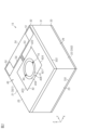
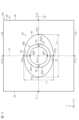
- FIG. 1 is a schematic plan view of an exemplary terahertz device according to a first embodiment.
- FIG. 2 is a schematic perspective view showing the terahertz device of FIG.
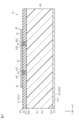
- FIG. 3 is a schematic cross-sectional view taken along line F3-F3 in FIG.
- FIG. 4 is a schematic plan view showing some components of the terahertz device of FIG.
- FIG. 5 is a schematic plan view showing the active element of the terahertz device of FIG. 1 and its periphery.
- FIG. 6 is a schematic plan view showing the active element of the terahertz device of FIG. 1 and its periphery.
- FIG. 7 is a schematic cross-sectional view showing the active element and its periphery shown in FIGS. FIG.
- FIG. 8 is a schematic plan view showing the resistor element of FIG. 1 and its periphery.
- FIG. 9 is a schematic cross-sectional view showing the resistor element of FIG. 8 and its periphery.
- FIG. 10 is a characteristic diagram showing the conductance of the terahertz device of FIG.
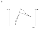
- FIG. 11 is a characteristic diagram showing the conductance and output power of the terahertz device of FIG.
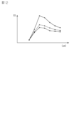
- FIG. 12 is a characteristic diagram showing the conductance of the terahertz device of FIG.
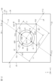
- FIG. 13 is a schematic plan view showing a terahertz device according to a modified example.
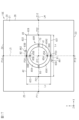
- FIG. 14 is a schematic plan view showing a terahertz device according to a modified example.
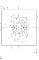
- FIG. 15 is a schematic plan view showing a terahertz device according to a modified example.
- FIG. 16 is a schematic plan view showing a terahertz device according to a modified example.
- FIG. 17 is a schematic plan view showing a terahertz device according to a modified example.
- FIG. 18 is a schematic plan view showing a terahertz device according to a modified example.
- FIG. 19 is a schematic plan view showing a terahertz device according to a modified example.
- FIG. 20 is a schematic plan view showing a terahertz device according to a modified example.
- FIG. 21 is a schematic plan view of an exemplary terahertz device according to the second embodiment.
- FIG. 22 is a schematic plan view showing the active element of the terahertz device of FIG. 21 and its periphery.
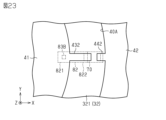
- FIG. 23 is a schematic plan view showing the active element of the terahertz device of FIG. 21 and its periphery.
- FIG. 24 is a schematic cross-sectional view showing the active element of FIG. 22 and its periphery.
- At least one means “one or more” of the desired options.
- at least one means “only one option” or “both of two options” if the number of options is two.
- at least one means “only one option” or “any combination of two or more options” if the number of options is three or more.
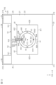
- FIG. 1 is a schematic plan view of an exemplary terahertz device 10 according to the first embodiment.
- FIG. 2 is a schematic perspective view of the terahertz device of FIG. 1.
- FIG. 3 is a schematic cross-sectional view taken along line F3-F3 of FIG. 1.
- FIG. 4 is a schematic plan view showing some components of the terahertz device 10 of FIG. 1, illustrating the arrangement of a first electrode 41, a second electrode 42, a first active element 60, a second active element 70, a first resistive element 81, and a second resistive element 82.
- the term "planar view” used in the present disclosure refers to viewing the terahertz device 10 in the Z-axis direction of the mutually orthogonal XYZ axes shown in FIG. 1.
- the terahertz device 10 includes a substrate 20.
- the substrate 20 is formed in a flat plate shape.
- the substrate 20 is formed in a rectangular parallelepiped shape.
- the substrate 20 includes a front surface 21, a back surface 22, and multiple side surfaces 23, 24, 25, and 26.
- the front surface 21 and the back surface 22 of the substrate 20 face opposite each other in the Z-axis direction. Therefore, "planar view” refers to viewing from a direction perpendicular to the front surface 21 of the substrate 20.
- perpendicular does not only mean strictly perpendicular, but also includes approximately perpendicular within the range in which the effect of this embodiment is achieved.
- the side surfaces 23 to 26 of the substrate 20 face either the X-axis direction or the Y-axis direction.
- the side surface 23 and the side surface 24 extend along the XZ plane.
- the side surface 23 and the side surface 24 face opposite each other in the Y-axis direction.
- the side surface 25 and the side surface 26 extend along the YZ plane. Side 25 and side 26 face opposite each other in the X-axis direction.
- the substrate 20 has a length Bx in the X-axis direction and a length By in the Y-axis direction.
- the length Bx in the X-axis direction can be 1 mm or less. In one example, the length Bx in the X-axis direction can be 500 ⁇ m.
- the length By in the Y-axis direction can be 1 mm or less. In one example, the length By in the Y-axis direction can be 500 ⁇ m.
- the substrate 20 includes a semiconductor substrate 31 and an insulating layer 32 on the semiconductor substrate 31 .
- the semiconductor substrate 31 is formed in a flat plate shape. As shown in Fig. 1, the shape of the semiconductor substrate 31 in a plan view is rectangular. In one example, the shape of the semiconductor substrate 31 in a plan view is square. Note that the shape of the semiconductor substrate 31 in a plan view is not limited to a rectangular shape, and may be a circular shape, an elliptical shape, or a polygonal shape.
- the semiconductor substrate 31 is formed of at least one semiconductor material selected from the group consisting of InP (indium phosphide), GaAs (gallium arsenide), AlGaAs (aluminum gallium arsenide), InGaAs (indium gallium arsenide), InGaAsP (indium gallium arsenide phosphide), Si (silicon), SiC (silicon carbide), GaN (gallium nitride), and single crystal AlN (aluminum nitride).
- the semiconductor substrate 31 is formed of a material containing InP.
- the semiconductor substrate 31 includes a substrate surface 311 and a substrate back surface 312.
- the substrate surface 311 and the substrate back surface 312 face in opposite directions.
- the substrate surface 311 faces the same side as the substrate surface 21, and the substrate back surface 312 faces the same side as the back surface 22.
- the semiconductor substrate 31 has substrate side surfaces that form part of each of the side surfaces 23 to 26. As the substrate surface 311 faces the same side as the substrate surface 21, the Z-axis direction is perpendicular to the substrate surface 311.
- the terahertz device 10 includes an insulating layer 32 provided on a semiconductor substrate 31.
- a substrate surface 311 of the semiconductor substrate 31 is covered with the insulating layer 32.
- the insulating layer 32 is made of an insulating material.
- the insulating layer 32 is made of a material including, for example, silicon oxide (SiO 2 ). In one example, the insulating layer 32 is formed over the entire substrate surface 311 of the semiconductor substrate 31.
- the insulating layer 32 has an insulating surface 321 and an insulating back surface 322 opposite the insulating surface 321.
- the insulating surface 321 faces the same side as the substrate surface 311, and the insulating back surface 322 faces the same side as the substrate back surface 312.
- the insulating surface 321 constitutes the surface 21.
- the insulating back surface 322 contacts the substrate surface 311 of the semiconductor substrate 31. Note that another member such as an insulating layer may be interposed between the substrate surface 311 of the semiconductor substrate 31 and the insulating layer 32.
- the insulating layer 32 has insulating side surfaces that constitute a part of each of the side surfaces 23 to 26.
- the terahertz device 10 includes a conductive layer 40 formed on the surface 21 of the substrate 20.
- the conductive layer 40 is formed on a portion of the surface 21 of the substrate 20.
- the conductive layer 40 is formed of at least one metal material selected from the group consisting of gold (Au), silver (Ag), aluminum (Al), copper (Cu), titanium (Ti), titanium nitride (TiN), and platinum (Pt). It can also be said that the conductive layer 40 contains at least one of Au, Ag, Al, Cu, Ti, and Pt.
- the conductive layer 40 is formed of a material containing Au.
- the conductive layer 40 is formed, for example, by sputtering.
- the conductive layer 40 may be formed of a laminated structure of multiple metal layers.
- the terahertz device 10 includes a slot 40A formed in the conductive layer 40.
- the slot 40A is formed in an annular shape in a planar view.
- the slot 40A is formed in an annular shape in a planar view.
- the terahertz device 10 includes an annular slot 40A.
- the conductive layer 40 includes a first electrode 41 partitioned by a slot 40A, and a second electrode 42 formed to surround the first electrode 41 via the slot 40A.
- the first electrode 41 is formed in a circular shape in a plan view.
- the first electrode 41 is disposed at the center of the substrate 20 in a plan view.
- the second electrode 42 is formed in a rectangular shape.
- the second electrode 42 includes a first side 421 and a second side 422 extending parallel to each other in a plan view, and a third side 423 and a fourth side 424 perpendicular to the first side 421 and the second side 422 in a plan view.
- the second electrode 42 is formed in a rectangular shape in which the lengths of the first side 421 and the second side 422 are greater than the lengths of the third side 423 and the fourth side 424. In one example, the second electrode 42 is disposed such that the first side 421 and the second side 422 extend in the X-axis direction in a plan view.
- the second electrode 42 may be in the shape of a square in which the lengths of the first side 421 and the second side 422 are equal to the lengths of the third side 423 and the fourth side 424.
- the second electrode 42 may be in the shape of a rectangle in which the lengths of the third side 423 and the fourth side 424 are greater than the lengths of the first side 421 and the second side 422.
- the terahertz device 10 includes a first active element 60 and a second active element 70 provided in the slot 40A.
- the first active element 60 and the second active element 70 are disposed in the slot 40A in a plan view. Therefore, it can be said that the first active element 60 and the second active element 70 are disposed between the first electrode 41 and the second electrode 42.
- the first active element 60 and the second active element 70 are elements that convert electromagnetic waves to electrical energy.
- electromagnetic waves include the concepts of either light or radio waves, or both.
- the first active element 60 and the second active element 70 are elements that oscillate electromagnetic waves (terahertz waves) in a specific frequency band, for example, the terahertz band.
- the first active element 60 and the second active element 70 can be said to be terahertz elements that oscillate terahertz waves.
- the first active element 60 and the second active element 70 are elements that detect terahertz waves, which are electromagnetic waves in a specific frequency band, for example, the terahertz band.
- the first active element 60 and the second active element 70 can be said to be terahertz elements that receive terahertz waves.
- the frequency band of the terahertz waves is, for example, 0.1 THz to 10 THz.
- the first active element 60 and the second active element 70 convert the supplied electrical energy into electromagnetic waves by oscillating due to the supplied electrical energy. As a result, the first active element 60 and the second active element 70 oscillate electromagnetic waves in a desired frequency band.
- the first active element 60 and the second active element 70 also receive electromagnetic waves and convert the electromagnetic waves into electrical energy. As a result, the first active element 60 and the second active element 70 detect electromagnetic waves in a desired frequency band.
- the first active element 60 and the second active element 70 may be, for example, resonant tunneling diodes (RTDs).
- the first active element 60 and the second active element 70 may be diodes or transistors other than RTDs.
- Other active elements may be, for example, TUNNETT (Tunnel injection Transit Time) diodes, IMPATT (Impact Ionization Avalanche Transit Time) diodes, GaAs-based field effect transistors (FETs), GaN-based FETs, high electron mobility transistors (HEMTs), heterojunction bipolar transistors (HBTs), or complementary metal-oxide-semiconductor (CMOS) FETs.
- TUNNETT Tunnelnel injection Transit Time
- IMPATT Impact Ionization Avalanche Transit Time
- FETs GaAs-based field effect transistors
- HEMTs high electron mobility transistors
- HBTs heterojunction bipolar transistors
- CMOS complementary metal-oxide-semic
- the shape of the first active element 60 and the second active element 70 in a planar view is rectangular. Note that the shape of the first active element 60 and the second active element 70 in a planar view is not limited to a rectangular shape, and may be a circular shape, an elliptical shape, or a polygonal shape.
- the first active element 60 and the second active element 70 are connected between the first electrode 41 and the second electrode 42.
- the first active element 60 and the second active element 70 are arranged on a reference line LM passing through the center 41C of the first electrode 41 in a plan view, sandwiching the first electrode 41.
- the reference line LM is set to extend in the X-axis direction.
- the reference line LM is parallel to the first side 421 of the second electrode 42 in a plan view.
- the reference line LM is also parallel to the side surfaces 23 and 24 of the substrate 20 in a plan view. Note that "parallel" does not only mean strictly parallel, but also includes roughly parallel within the range in which the effect of this embodiment is achieved.
- the first active element 60 and the second active element 70 are connected to the first electrode 41 and the second electrode 42 so that they oscillate in a phase inverted state (opposite phase).
- the first active element 60 and the second active element 70 are connected between the first electrode 41 and the second electrode 42 so that they are in parallel.
- the first active element 60 is connected between the second electrode 42 and the first electrode 41.
- the conductive layer 40 includes a connection portion 441 extending from the second electrode 42 toward the first electrode 41.
- the conductive layer 40 also includes a connection portion 431 extending from the first electrode 41 toward the second electrode 42.
- the first active element 60 is connected between the second electrode 42 and the first electrode 41 by the connection portion 441 and the connection portion 431.
- the second active element 70 is connected between the first electrode 41 and the second electrode 42.
- the conductive layer 40 includes a connection portion 432 extending from the first electrode 41 toward the second electrode 42.
- the conductive layer 40 includes a connection portion 442 extending from the second electrode 42 toward the first electrode 41.
- the second active element 70 is connected between the first electrode 41 and the second electrode 42 by the connection portion 432 and the connection portion 442.
- the terahertz device 10 includes a first resistive element 81 and a second resistive element 82.
- the first resistive element 81 and the second resistive element 82 are provided outside the slot 40A.
- the first resistive element 81 and the second resistive element 82 are arranged at a position overlapping the second electrode 42 in a planar view.
- the first resistive element 81 and the second resistive element 82 are arranged on either side of the first electrode 41.
- the first resistive element 81 and the second resistive element 82 are arranged at a symmetrical position with respect to the first electrode 41.
- the first resistive element 81 and the second resistive element 82 are arranged at a point symmetrical position with the center 41C of the first electrode 41 as the center.
- the first resistive element 81 and the second resistive element 82 are electrically connected in parallel to the first active element 60 and the second active element 70.
- the first resistive element 81 and the second resistive element 82 suppress parasitic oscillation. This makes it possible to stabilize oscillation in the terahertz device 10.
- the first resistor element 81 and the second resistor element 82 are electrically connected to the first electrode 41 at virtual short points 45A and 45B. It can be said that the first resistor element 81 and the second resistor element 82 are connected to both ends of the first electrode 41 on the auxiliary straight line LS that passes through the center 41C of the first electrode 41.
- the virtual short-circuit points 45A and 45B are portions where the electric field strength of the terahertz waves generated by the first active element 60 and the second active element 70, which oscillate in opposite phases, is relatively low, and can be said to be pseudo short-circuit points.
- the virtual short-circuit points 45A and 45B may be set in a range where the electric field strength of the terahertz waves is relatively low.
- the electric fields generated by the first active element 60 and the second active element 70, which oscillate in opposite phases, are added together in opposite phases. As a result, a portion where the electric field strength is relatively low occurs near the center between the first active element 60 and the second active element 70.
- the place where the electric field strength is relatively low occurs at an equal distance from the first active element 60 and the second active element 70.
- the place where the electric field strength is relatively low occurs along the auxiliary straight line LS that is perpendicular to the reference straight line LM that passes through the first active element 60 and the second active element 70 and passes through the center 41C of the first electrode 41, as shown in FIG. 4.
- FIG. 5 is a schematic plan view of an enlarged portion of the terahertz device 10 in Fig. 1, showing the arrangement of the first active element 60.
- Fig. 6 is a schematic plan view of an enlarged portion of the terahertz device 10 in Fig. 1, showing the arrangement of the second active element 70.
- Fig. 7 is a schematic cross-sectional view showing the first active element 60, the second active element 70 and their periphery.
- the first active element 60 is provided between the second electrode 42 and the semiconductor substrate 31 in the Z-axis direction.
- a semiconductor layer 61a is provided on the substrate surface 311 of the semiconductor substrate 31.
- the shape of the semiconductor layer 61a is rectangular in a plan view.
- the semiconductor layer 61a is formed of, for example, GaInAs.
- the semiconductor layer 61a is highly doped with n-type impurities.
- a GaInAs layer 62a is stacked on the semiconductor layer 61a.
- the GaInAs layer 62a is doped with n-type impurities.
- the n-type impurity concentration of the GaInAs layer 62a is lower than the n-type impurity concentration of the semiconductor layer 61a.
- a GaInAs layer 63a is stacked on the GaInAs layer 62a.
- the GaInAs layer 63a is not doped with impurities.
- An AlAs layer 64a is stacked on the GaInAs layer 63a.
- An InGaAs layer 65 is stacked on the AlAs layer 64a.
- the InGaAs layer 65 is not doped with impurities.
- An AlAs layer 64b is stacked on the InGaAs layer 65.
- the AlAs layer 64a, InGaAs layer 65, and AlAs layer 64b form a resonant tunnel section.
- a GaInAs layer 63b that is not doped with impurities is stacked on the AlAs layer 64b.
- a GaInAs layer 62b that is doped with n-type impurities is stacked on the GaInAs layer 63b.
- a GaInAs layer 61b that is doped with a high concentration of n-type impurities is stacked on the GaInAs layer 62b. Therefore, the n-type impurity concentration of the GaInAs layer 61b is higher than the n-type impurity concentration of the GaInAs layer 62b.
- the specific configuration of the first active element 60 can be changed as desired as long as it is capable of generating (or detecting, or both) electromagnetic waves.
- the first active element 60 may be anything that performs at least one of oscillation and detection of electromagnetic waves in the terahertz band.
- connection portion 441 extending from the second electrode 42 extends toward the semiconductor layer 61a and is electrically connected to the semiconductor layer 61a.
- connection portion 431 extending from the first electrode 41 contacts the upper surface of the GaInAs layer 61b and is electrically connected to the GaInAs layer 61b. In this manner, the first active element 60 is connected between the second electrode 42 and the first electrode 41.
- the second active element 70 is provided between the first electrode 41 and the semiconductor substrate 31 in the Z-axis direction.
- a semiconductor layer 71a is provided on the substrate surface 311 of the semiconductor substrate 31.
- the shape of the semiconductor layer 71a is rectangular in a plan view.
- the semiconductor layer 71a is formed of, for example, GaInAs.
- the semiconductor layer 71a is highly doped with n-type impurities.
- a GaInAs layer 72a is stacked on the semiconductor layer 71a.
- the GaInAs layer 72a is doped with n-type impurities.
- the n-type impurity concentration of the GaInAs layer 72a is lower than the n-type impurity concentration of the semiconductor layer 71a.
- a GaInAs layer 73a is stacked on the GaInAs layer 72a.
- the GaInAs layer 73a is not doped with impurities.
- An AlAs layer 74a is stacked on the GaInAs layer 73a.
- An InGaAs layer 75 is stacked on the AlAs layer 74a.
- the InGaAs layer 75 is not doped with impurities.
- An AlAs layer 74b is stacked on the InGaAs layer 75.
- the AlAs layer 74a, InGaAs layer 75, and AlAs layer 74b form a resonant tunnel section.
- a GaInAs layer 73b that is not doped with impurities is stacked on the AlAs layer 74b.
- a GaInAs layer 72b that is doped with n-type impurities is stacked on the GaInAs layer 73b.
- a GaInAs layer 71b that is doped with a high concentration of n-type impurities is stacked on the GaInAs layer 72b. Therefore, the n-type impurity concentration of the GaInAs layer 71b is higher than the n-type impurity concentration of the GaInAs layer 72b.
- the specific configuration of the second active element 70 can be changed as desired as long as it is capable of generating (or detecting, or both) electromagnetic waves.
- the second active element 70 may be anything that performs at least one of oscillation and detection of electromagnetic waves in the terahertz band.
- connection portion 432 extending from the first electrode 41 contacts the upper surface of the GaInAs layer 71b and is electrically connected to the GaInAs layer 71b.
- connection portion 442 extending from the second electrode 42 extends toward the semiconductor layer 71a and is electrically connected to the semiconductor layer 71a. In this manner, the second active element 70 is connected between the first electrode 41 and the second electrode 42.
- Fig. 8 is a schematic plan view showing an enlarged portion of the terahertz device 10 in Fig. 1, illustrating the arrangement of the first resistor element 81.
- Fig. 9 is a schematic cross-sectional view showing the first resistor element 81 in Fig. 8 and its periphery.
- the first resistor element 81 is provided between the semiconductor substrate 31 and the second electrode 42.
- the first resistor element 81 is provided on the substrate surface 311 of the semiconductor substrate 31.
- the shape of the first resistor element 81 is rectangular in a plan view.
- the first resistor element 81 is composed of a semiconductor layer doped with a high concentration of n-type impurities.
- the semiconductor layer may be GaInAs.
- the first resistive element 81 includes a first end 811 and a second end 812 opposite the first end.
- the first end 811 is electrically connected to the second electrode 42 by a via 83A formed on the first resistive element 81.
- the via 83A is formed of at least one metal material selected from the group consisting of Au, Ag, Al, Cu, Ti, TiN, and Pt. It can also be said that the via 83A includes at least one of Au, Ag, Al, Cu, Ti, and Pt. In one example, the via 83A is formed of a material including Au.
- the lower wiring 84A is electrically connected to the second end 812 of the first resistor element 81.
- the lower wiring 84A is disposed in the insulating layer 32 in the Z-axis direction. It can be said that the lower wiring 84A is disposed between the insulating front surface 321 and the insulating back surface 322 in the Z-axis direction.
- the insulating layer 32 may include a first insulating film formed on the semiconductor substrate 31 and a second insulating film formed on the first insulating film.
- the first insulating film may be formed, for example, with the same film thickness as the first resistor element 81.
- the lower wiring 84A may be formed on the first insulating film.
- the insulating layer 32 may include three or more insulating films.
- the lower wiring 84A is formed of at least one metal material selected from the group consisting of Au, Ag, Al, Cu, Ti, TiN, and Pt. It can also be said that the lower wiring 84A includes at least one of Au, Ag, Al, Cu, Ti, and Pt. In one example, the lower wiring 84A is made of a material containing Au.
- the lower wiring 84A extends toward the first electrode 41. It can be said that the lower wiring 84A extends so as to intersect with the slot 40A between the second electrode 42 and the first electrode 41.
- the lower wiring 84A is electrically connected to the first electrode 41 by a via 85A.
- the via 85A electrically connecting the lower wiring 84A and the first electrode 41 is disposed at the virtual short point 45A.
- the via 85A is formed of at least one metal material selected from the group consisting of Au, Ag, Al, Cu, Ti, TiN, and Pt. It can also be said that the via 85A includes at least one of Au, Ag, Al, Cu, Ti, and Pt. In one example, the via 85A is formed of a material including Au.
- the second resistor element 82 is electrically connected to the first electrode 41 and the second electrode 42, similar to the first resistor element 81.
- the second resistor element 82 is provided on the substrate surface 311 of the semiconductor substrate 31.
- the shape of the second resistor element 82 is rectangular in a plan view.
- the second resistor element 82 is composed of a semiconductor layer doped with a high concentration of n-type impurities.
- the semiconductor layer may be GaInAs.
- the second resistive element 82 includes a first end 821 and a second end 822 opposite to the first end.
- the first end 821 is electrically connected to the second electrode 42 by a via 83B formed on the second resistive element 82.
- the via 83B is formed of at least one metal material selected from the group consisting of Au, Ag, Al, Cu, Ti, TiN, and Pt. It can also be said that the via 83B includes at least one of Au, Ag, Al, Cu, Ti, and Pt. In one example, the via 83B is formed of a material including Au.
- the lower wiring 84B is electrically connected to the second end 822 of the second resistor element 82.
- the lower wiring 84B is disposed in the insulating layer 32 in the Z-axis direction. It can be said that the lower wiring 84B is disposed between the insulating front surface 321 and the insulating back surface 322 in the Z-axis direction.
- the insulating layer 32 may include a first insulating film formed on the semiconductor substrate 31 and a second insulating film formed on the first insulating film.
- the first insulating film may be formed with the same film thickness as the second resistor element 82, for example.
- the lower wiring 84B may be formed on the first insulating film. Note that the insulating layer 32 may include three or more insulating films.
- the lower wiring 84B is formed of at least one metal material selected from the group consisting of Au, Ag, Al, Cu, Ti, TiN, and Pt. It can also be said that the lower wiring 84B includes at least one of Au, Ag, Al, Cu, Ti, and Pt. In one example, the lower wiring 84B is made of a material containing Au.
- the lower wiring 84B extends toward the first electrode 41.
- the lower wiring 84B can be said to extend so as to intersect with the slot 40A between the second electrode 42 and the first electrode 41.
- the lower wiring 84B is electrically connected to the first electrode 41 by a via 85B.
- the via 85B electrically connecting the lower wiring 84B and the first electrode 41 is disposed at the virtual short point 45B.
- the via 85B is formed of at least one metal material selected from the group consisting of Au, Ag, Al, Cu, Ti, TiN, and Pt.
- the via 85B can also be said to include at least one of Au, Ag, Al, Cu, Ti, and Pt.
- the via 85B is formed of a material including Au.
- the terahertz device 10 includes a first electrode pad 51 and a second electrode pad 52 provided on the surface 21 of the substrate 20.
- the first electrode pad 51 and the second electrode pad 52 are arranged at the edge of the substrate 20.
- the first electrode pad 51 and the second electrode pad 52 are arranged along the side surface 24 on the surface 21 of the substrate 20.
- the first electrode pad 51 is arranged at a corner portion 21A formed by the side surface 24 and the side surface 26 on the surface 21 of the substrate 20.
- the second electrode pad 52 is arranged at a corner portion 21B formed by the side surface 24 and the side surface 25 on the surface 21 of the substrate 20.
- the terahertz device 10 also includes a first connection wiring 53 that connects the first electrode pad 51 and the first electrode 41.
- the first connection wiring 53 electrically connects the first electrode pad 51 and the first electrode 41.
- the first connection wiring 53 is preferably connected to the first electrode 41 at the virtual short-circuit point 45B. In this way, by connecting the first connection wiring 53 to the first electrode 41 at the virtual short-circuit point 45B, leakage of electromagnetic waves to the first connection wiring 53 can be suppressed.
- the first connection wiring 53 includes a first wiring 531, a second wiring 532, a lower wiring 533, and a via 534.
- the first wiring 531 extends in the X-axis direction from the first electrode pad 51.
- the second wiring 532 extends in the Y-axis direction from the tip of the first wiring 531.
- the via 534 is connected to the tip of the second wiring 532.
- the lower wiring 533 is connected to the second wiring 532 by the via 534 and is electrically connected to the lower wiring 84B.
- the first connection wiring 53 electrically connects the first electrode pad 51 and the first electrode 41 by the lower wiring 84B and the via 85B.
- the first connection wiring 53 connects the first electrode pad 51 to the virtual short point 45B of the first electrode 41.
- the lower wiring 533 of the first connection wiring 53 may be arranged on a path different from the lower wiring 84B and connected to the first electrode 41.
- the terahertz device 10 includes a second connection wiring 54 that connects the second electrode pad 52 and the second electrode 42.
- the second connection wiring 54 electrically connects the second electrode pad 52 and the second electrode 42.
- the second connection wiring 54 is preferably connected to the second electrode 42 at a virtual short point.
- the second connection wiring 54 includes a first wiring 541 and a second wiring 542.
- the first wiring 541 extends from the second electrode pad 52 in the X-axis direction.
- the second wiring 542 extends from the tip of the first wiring 541 in the Y-axis direction.
- the second wiring 542 extends from the tip of the first wiring 541 toward the second electrode 42 and is electrically connected to the second electrode 42.
- the second electrode pad 52 is connected to the second electrode 42 by the second connection wiring 54 in the vicinity of the auxiliary straight line LS that is the virtual short point. In this way, by connecting the second connection wiring 54 near the virtual short point, it is possible to suppress leakage of electromagnetic waves to the second connection wiring 54.
- the terahertz device 10 includes a reflective layer 33 provided on the rear surface 22 of the substrate 20.
- the reflective layer 33 is in contact with the rear surface 22 of the substrate 20.
- the reflective layer 33 includes a reflective surface 331 and a reflective rear surface 332 opposite to the reflective surface 331.
- the reflective surface 331 faces the same direction as the substrate front surface 311.
- the reflective rear surface 332 faces the same direction as the substrate rear surface 312.
- the reflective layer 33 has a thickness capable of reflecting electromagnetic waves generated or detected by the first active element 60 and the second active element 70.
- the reflective layer 33 is composed of a metal layer provided on the rear surface 22 of the substrate 20.
- the reflective layer 33 is formed of at least one metal material selected from the group consisting of Au, Ag, Al, Cu, Ti, TiN, and Pt. It can also be said that the reflective layer 33 contains at least one of Au, Ag, Al, Cu, Ti, and Pt.
- the reflective layer 33 is formed of a material containing Au.
- the reflective layer 33 may be formed of the same material as the conductive layer 40.
- the reflective layer 33 is formed, for example, by sputtering.
- the reflective layer 33 may be composed of a laminated structure of multiple metal layers.
- the terahertz device 10 includes a substrate 20, a conductive layer 40, a slot 40A, a first active element 60, and a second active element 70.
- the substrate 20 includes a front surface 21 and a back surface 22, and the conductive layer 40 is formed in a part of the front surface 21.
- the slot 40A is formed in the conductive layer 40.
- the slot 40A is formed in an annular shape.
- the first active element 60 and the second active element 70 are provided in the slot 40A.
- the conductive layer 40 includes a first electrode 41 partitioned by the slot 40A, and a second electrode 42 formed to surround the first electrode 41 via the slot 40A.
- An end face of the conductive layer 40 (the first electrode 41 and the second electrode 42) facing the annular slot 40A constitutes a ring slot antenna 40R.
- the distance L12 between the first active element 60 and the second active element 70 in the circumferential direction of the slot 40A is equal to 1/2 the effective wavelength ⁇ g of the terahertz waves generated by the first active element 60 and the second active element 70.
- “equal” includes cases where the compared objects have some difference due to the influence of dimensional tolerances, etc., in addition to cases where they are exactly equal.
- the effective wavelength ⁇ g is the wavelength of the terahertz waves propagating inside the terahertz device 10.
- the size (radius) of the slot 40A is set corresponding to the distance L12 between the first active element 60 and the second active element 70. In one example, the radius of the slot 40A may be 30 ⁇ m.
- the first active element 60 and the second active element 70 are arranged on a reference line LM that passes through the center 41C of the first electrode 41. It can be said that this terahertz device 10 includes two oscillators consisting of two semicircular slots 40A1, 40A2 and the first active element 60 and the second active element 70 arranged in each semicircular slot 40A1, 40A2.
- the first electrode 41 and the second electrode 42 facing the semicircular slots 40A1, 40A2 in which the first active element 60 and the second active element 70 are arranged respectively constitute a slot antenna.
- the polarization direction of the terahertz wave generated by the slot antenna of the terahertz device 10 coincides with the extension direction of the reference line LM on which the first active element 60 and the second active element 70 are arranged.
- the second electrode 42 includes a first end P21 and a second end P22, which are opposite ends on the reference line LM in a plan view.
- the second electrode 42 has a first distance Lx between the first end P21 and the second end P22.
- the first distance Lx can be said to be the electrode size of the second electrode 42 in the polarization direction (the direction along the reference line LM).
- the substrate 20 includes a first substrate end P11 and a second substrate end P12, which are opposite ends on the reference line LM.
- the substrate 20 has a first substrate distance Cx between the first substrate end P11 and the second substrate end P12.
- the first substrate distance Cx can be said to be the substrate size of the substrate 20 in the polarization direction (the direction along the reference line LM).
- the first distance Lx of the second electrode 42 is smaller than the first substrate distance Cx of the substrate 20. It can be said that the terahertz device 10 includes a second electrode 42 with a first distance Lx (electrode size) smaller than the first substrate distance Cx of the substrate 20. This changes the standing wave distribution in the second electrode 42. The standing wave distribution affects the impedance at the locations where the first active element 60 and the second active element 70 are arranged. Therefore, the impedance can be adjusted by changing the standing wave distribution, that is, by changing the first distance Lx of the second electrode 42.
- Figure 10 shows an example of the overall conductance of the terahertz device 10 versus the first distance Lx at the resonant frequency.
- the horizontal axis is the first distance Lx
- the vertical axis is the conductance (S).
- the characteristics shown in Figure 10 are for a case where the radius of the slot 40A is 30 ⁇ m.
- the second electrode 42 includes a third end P23 and a fourth end P24 on an auxiliary line LS that is perpendicular to the reference line LM and passes through the center 41C of the first electrode 41 in a plan view.
- the second electrode 42 has a second distance Ly between the third end P23 and the fourth end P24.
- the second distance Ly can be said to be the electrode size of the second electrode 42 in a direction perpendicular to the polarization direction (the direction along the auxiliary line LS).
- the second distance Ly may be the same as the first distance Lx.
- the second distance Ly may be smaller than the first distance Lx, or may be larger than the first distance Lx.
- the substrate 20 includes a third substrate end P13 and a fourth substrate end P14, which are opposite ends on the auxiliary line LS.
- the substrate 20 has a second substrate distance Cy between the third substrate end P13 and the fourth substrate end P14.
- the second substrate distance Cy can be said to be the substrate size of the substrate 20 in a direction perpendicular to the polarization direction (the direction along the auxiliary line LS).
- the second distance Ly of the second electrode 42 is smaller than the second substrate distance Cy of the substrate 20. It can be said that the terahertz device 10 includes a second electrode 42 with a second distance Ly (electrode size) smaller than the second substrate distance Cy of the substrate 20. This changes the standing wave distribution in the second electrode 42. The standing wave distribution affects the impedance at the locations where the first active element 60 and the second active element 70 are arranged. Therefore, the impedance can be adjusted by changing the standing wave distribution, that is, by changing the second distance Ly of the second electrode 42.
- FIG. 12 shows an example of the calculation result of the overall conductance of the terahertz device 10 with respect to the first distance Lx when the second distance Ly is changed at the resonant frequency.
- the horizontal axis is the first distance Lx
- the vertical axis is the conductance (S).
- the characteristics shown in FIG. 12 are for a case in which the radius of the slot 40A is 30 ⁇ m.
- the solid line, dashed line, and dashed line show the conductance at different second distances Ly.
- the second distance Ly is increased in the order of the solid line, dashed line, and dashed line.
- Figure 11 shows an example of the overall conductance of the terahertz device 10 and the power of the terahertz waves generated by the terahertz device 10 when the first distance Lx is changed at the resonant frequency.
- the horizontal axis represents the first distance Lx
- the vertical axis represents the conductance and the power of the terahertz waves. Note that the characteristics shown in Figure 11 are for a second distance Ly of 100 ⁇ m.
- the solid line represents the conductance, and the dashed line represents the power.
- the terahertz device 10 includes a substrate 20, a conductive layer 40, a slot 40A, a first active element 60, and a second active element 70.
- the substrate 20 includes a front surface 21 and a back surface 22, and the conductive layer 40 is formed in a part of the front surface 21.
- the slot 40A is formed in the conductive layer 40.
- the slot 40A is formed in an annular shape.
- the first active element 60 and the second active element 70 are provided in the slot 40A.
- the conductive layer 40 includes a first electrode 41 partitioned by the slot 40A, and a second electrode 42 formed to surround the first electrode 41 via the slot 40A.
- the standing wave distribution in the second electrode 42 changes.
- the standing wave distribution affects the impedance at the locations where the first active element 60 and the second active element 70 are arranged.
- the impedance can be adjusted.
- the output power (output electric power) of the terahertz device 10 can be improved, that is, a higher output can be achieved.
- the second distance Ly between the third end P23 and the fourth end P24, which are both ends of the second electrode 42 on the auxiliary line LS that passes through the center 41C of the first electrode 41 and is perpendicular to the reference line LM, is smaller than the second substrate distance Cy between the third substrate end P13 and the fourth substrate end P14, which are both ends of the substrate 20 on the auxiliary line LS.
- the standing wave distribution in the second electrode 42 changes. The standing wave distribution affects the impedance at the locations where the first active element 60 and the second active element 70 are arranged. As a result, the impedance can be adjusted.
- the first active element 60 and the second active element 70 are connected in parallel. Therefore, by oscillating the first active element 60 and the second active element 70 in opposite phases, the output power (output electric power) of the terahertz device 10 can be improved.
- (1-4) Includes a first resistive element 81 and a second resistive element 82 connected in parallel to the first active element 60 and the second active element 70. This allows the oscillation to be stabilized in the terahertz device 10.
- the terahertz device 10 includes a reflective layer 33 provided on the rear surface 312 of the semiconductor substrate 31.
- the reflective layer 33 reflects electromagnetic waves radiated from the ring slot antenna 40R toward the semiconductor substrate 31. Therefore, the terahertz device 10 can radiate electromagnetic waves in the direction in which the substrate front surface 311 of the substrate 20 faces.
- the first electrode pad 51 and the second electrode pad 52 may be disposed at the corners 21A and 21B of the substrate 20. This configuration makes it possible to prevent the first electrode pad 51 and the second electrode pad 52 from blocking the electromagnetic waves reflected by the reflective layer 33 and heading toward the surface 21.
- the first electrode pad 51 is connected to the first electrode 41 by a first connection wiring 53.
- the first connection wiring 53 is connected to the virtual short point 45B of the first electrode 41. By connecting the first connection wiring 53 to the virtual short point 45B, leakage of electromagnetic waves to the first connection wiring 53 can be suppressed.
- the second electrode pad 52 is connected to the second electrode 42 by the second connection wiring 54.
- the second connection wiring 54 is connected to the second electrode 42 near the auxiliary straight line LS, which is a virtual short-circuit point.
- the first embodiment can be modified, for example, as follows.
- the first embodiment can be combined with the following modifications as long as no technical contradiction occurs.
- the same reference numerals as in the first embodiment are used for the parts common to the first embodiment, and the description thereof will be omitted.
- the terahertz device 10A of the modified example includes an elliptical second electrode 42.
- the second electrode 42 includes a first end P21 and a second end P22 on the reference line LM.
- the second electrode 42 also includes a third end P23 and a fourth end P24 on the auxiliary line LS.
- the second electrode 42 has an elliptical shape in which the first distance Lx between the first end P21 and the second end P22 is greater than the second distance Ly between the third end P23 and the fourth end P24.
- the second electrode 42 of this terahertz device 10A does not have corners, unlike the second electrode 42 of the first embodiment. Therefore, in this terahertz device 10A, radiation from the outer circumferential end of the second electrode 42 can be suppressed, and the radiation pattern can be improved.
- the second electrode 42 may be circular in shape with the first distance Lx and the second distance Ly being equal.
- the second electrode 42 may be elliptical in shape with the first distance Lx being smaller than the second distance Ly.
- the shape of the second electrode 42 may be any shape other than elliptical, such as a polygon, a rhombus, a trapezoid, an oval, or the like.
- the modified terahertz device 10B differs from the first embodiment in the arrangement of the first active element 60 and the second active element 70.
- the reference line LM passing through the center 41C of the first electrode 41 is inclined with respect to the first side 421 and the second side 422 of the second electrode 42 in a planar view.
- the first side 421 and the second side 422 of the second electrode 42 are parallel to the side surface 23 and the side surface 24 of the substrate 20.
- the first active element 60 and the second active element 70 are arranged on the reference line LM with the first electrode 41 in between.
- the first active element 60 and the second active element 70 are arranged at positions rotated in the X-axis direction and the Y-axis direction around the center 41C of the first electrode 41.
- the terahertz device 10B of this modified example can adjust the first distance Lx and the second distance Ly by changing the rotation angle of the first active element 60 and the second active element 70, that is, the angle of the reference line LM relative to the first side 421 and the second side 422 of the second electrode 42.
- the terahertz device 10B of the modified example can adjust the impedance by changing the inclination of the reference line LM that indicates the polarization direction by the first active element 60 and the second active element 70, without changing the size of the second electrode 42.
- the modified terahertz device 10C includes a rectangular second electrode 42.
- a first side 421 and a second side 422 of the second electrode 42 are inclined with respect to the side surface 23 and the side surface 24 of the substrate 20.
- the reference line LM is parallel to the first side 421 of the second electrode 42.
- the second electrode 42 may be inclined with respect to the substrate 20 in a planar view.
- the modified terahertz device 10C can change the first substrate distance Cx between the first substrate end P11 and the second substrate end P12, which are both ends of the substrate 20, by the angle of the second electrode 42, i.e., the angle of the reference line LM.
- the modified terahertz device 10D includes a rectangular second electrode 42.
- the first side 421 and the second side 422 of the second electrode 42 are parallel to the side surfaces 23 and 24 of the substrate 20.
- the second electrode 42 is disposed closer to the side surfaces 23 and 26 of the substrate 20.
- the second electrode 42 includes a first end P21 and a second end P22 on the reference line LM.
- the distance LC1 from the center 41C of the first electrode 41 to the first end P21 is smaller than the distance LC2 from the center 41C of the first electrode 41 to the second end P22.
- the second electrode 42 also includes a third end P23 and a fourth end P24 on the auxiliary line LS.
- the distance LC3 from the center 41C of the first electrode 41 to the third end P23 is larger than the distance LC4 from the center 41C of the first electrode 41 to the fourth end P24.
- the second electrode 42 can be said to be arranged asymmetrically with respect to the center 41C of the first electrode 41.
- the admittance of the first active element 60 and the second active element 70 are asymmetric.
- impedance matching can be performed for each of the active elements of different mesa sizes.
- the first resistor element 81 and the second resistor element 82 are arranged outside the second electrode 42.
- the first resistor element 81 is arranged to extend along the first side 421 of the second electrode 42
- the second resistor element 82 is arranged to extend along the second side 422 of the second electrode 42. It can be said that the first resistor element 81 and the second resistor element 82 are arranged at positions that do not overlap with the second electrode 42.
- the second electrode 42 includes resistor connection portions 461, 462 that protrude in the Y-axis direction from the first side 421 and the second side 422.
- the first resistor element 81 and the second resistor element 82 are electrically connected to the second electrode 42 by vias 83A, 83B and the resistor connection portions 461, 462.
- the second distance Ly of the second electrode 42 can be made smaller.
- the first resistor element 81 and the second resistor element 82 are arranged at an angle with respect to the first side 421 and the second side 422 of the second electrode 42.
- the first resistor element 81 and the second resistor element 82 are arranged so that a portion of each of them overlaps with the second electrode 42. It can be said that the first resistor element 81 and the second resistor element 82 are arranged so that a portion of each of them is located outside the second electrode 42.
- the first resistor element 81 and the second resistor element 82 are electrically connected to the second electrode 42 by vias 83A and 83B arranged at positions overlapping with the second electrode 42.
- the modified terahertz device 10G includes an upper wiring 55 arranged to straddle the slot 40A. More specifically, the modified terahertz device 10G includes a first connection wiring 53 that electrically connects the first electrode pad 51 and the first electrode 41.
- the first connection wiring 53 includes a first wiring 531, a second wiring 532, an upper wiring 55, and vias 561 and 562.
- the terahertz device 10G includes an insulating layer 57 formed on the conductive layer 40.
- the upper wiring 55 is formed on the insulating layer 57.
- the upper wiring 55 is electrically connected to the second wiring 532 by a via 561 that penetrates the insulating layer 57.
- the upper wiring 55 is electrically connected to the first electrode 41 by a via 562 that penetrates the insulating layer 57.
- the via 562 may be disposed at the virtual short point 45B.
- the first resistive element 81 and the second resistive element 82 may be electrically connected to the first electrode 41 by a configuration similar to the upper wiring 55 shown in FIG. 19.
- the first resistive element 81 and the second resistive element 82 may be electrically connected to the first electrode 41 by a configuration similar to the upper wiring 55 shown in FIG. 19.
- the modified terahertz device 10H includes a second electrode pad 52 arranged diagonally from the first electrode pad 51.
- the second electrode pad 52 is arranged at a corner 21C formed by side 23 and side 25 on the surface 21 of the substrate 20.
- the second electrode pad 52 is on the opposite side of the center 41C of the first electrode 41 from the virtual short-circuit point 45B of the first electrode 41 to which the first electrode pad 51 is connected, and is electrically connected to the second electrode 42 at the virtual short-circuit point 45C of the second electrode 42.
- the second electrode pad 52 is electrically connected to the first side 421 of the second electrode 42 by the second connection wiring 54. In this way, by connecting the second connection wiring 54 to the second electrode 42 at the virtual short-circuit point 45C, it is possible to further reduce the leakage of electromagnetic waves to the second connection wiring 54.
- the second electrode pad 52 may be disposed at the corner 21D formed by the side surface 23 and the side surface 26 on the surface 21 of the substrate 20, as shown by the dashed line in FIG. 20.
- Fig. 21 is a schematic plan view of an exemplary terahertz device 100 according to the second embodiment.
- Fig. 22 is a schematic plan view showing some components of the terahertz device 100 of Fig. 21, showing a first active element 60 and a first resistive element 81.
- Fig. 23 is a schematic plan view showing some components of the terahertz device 100 of Fig. 21, showing a second active element 70 and a second resistive element 82.
- Fig. 24 is a schematic cross-sectional view showing the first active element 60 and the first resistive element 81 of Fig. 21.
- the terahertz device 100 of the second embodiment includes a first resistive element 81 and a second resistive element 82 arranged to overlap the first active element 60 and the second active element 70 in a planar view.
- the first resistive element 81 is connected in parallel to the first active element 60.
- the second resistive element 82 is connected in parallel to the second active element 70.
- the first resistor element 81 is arranged so as to overlap the first active element 60 in a planar view.
- the first resistor element 81 includes a first end 811 and a second end 812.
- the second end 812 of the first resistor element 81 is electrically connected to the first active element 60.
- the first end 811 of the first resistor element 81 is arranged so as to overlap the first electrode 41.
- the first end 811 of the first resistor element 81 is electrically connected to the first electrode 41 by a via 83A.
- the second resistive element 82 is arranged so as to overlap with the second active element 70 in a planar view.
- the second resistive element 82 includes a first end 821 and a second end 822.
- the second end 822 of the second resistive element 82 is electrically connected to the second active element 70.
- the first end 821 of the second resistive element 82 is arranged so as to overlap with the first electrode 41.
- the first end 821 of the second resistive element 82 is electrically connected to the first electrode 41 by a via 83B.
- the first resistor element 81 is formed on the substrate surface 311 of the semiconductor substrate 31.
- the first resistor element 81 is disposed adjacent to the semiconductor layer 61a of the first active element 60.
- the GaInAs layer 62a of the first active element 60 is disposed so as to overlap both the semiconductor layer 61a and the first resistor element 81.
- the semiconductor layer 61a and the first resistor element 81 may be made of the same material.
- the semiconductor layer 61a and the first resistor element 81 are made of GaInAs.
- the semiconductor layer 61a and the first resistor element 81 may be doped with a high concentration of n-type impurities.
- the first resistor element 81 may be formed integrally with the semiconductor layer 61a.
- the boundary between the semiconductor layer 61a and the first resistor element 81 is shown by a dashed line, but this dashed line does not necessarily mean that there is an actually identifiable boundary.
- the second resistor element 82 is configured in the same way as the first resistor element 81.
- the terahertz device 100 of the second embodiment functions as a detector that detects terahertz waves.
- the first resistor element 81 is electrically connected in parallel to the first active element 60.
- the second resistor element 82 is electrically connected in parallel to the second active element 70.
- the first resistor element 81 and the second resistor element 82 of the second embodiment can suppress oscillation of the first active element 60 and the second active element 70.
- the terahertz device 100 of the second embodiment includes a first active element 60 and a second active element 70 arranged on either side of the first electrode 41, similar to the terahertz device 10 of the first embodiment, and is capable of adjusting impedance.
- the terahertz device 100 of the second embodiment detects terahertz waves by the first active element 60 and the second active element 70. Therefore, the terahertz device 100 of the second embodiment can improve the resolution.
- the terahertz device 100 of the second embodiment includes a first resistive element 81 arranged to overlap the first active element 60, and a second resistive element 82 arranged to overlap the second active element 70.
- the first resistive element 81 and the second resistive element 82 suppress the oscillation of the first active element 60 and the second active element 70. Therefore, the terahertz device 100 of the second embodiment can suppress the oscillation of the first active element 60 and the second active element 70.
- the reflective layer 33 may be omitted.
- the semiconductor substrate 31 may be made up of multiple laminated substrates.
- the term "on” as used in this disclosure includes both the meanings of "on” and “above,” unless the context clearly indicates otherwise.
- the phrase “a first layer is formed on a second layer” is intended to mean that in some embodiments, the first layer may be disposed directly on the second layer in contact with the second layer, while in other embodiments, the first layer may be disposed above the second layer without contacting the second layer. That is, the term “on” does not exclude a structure in which another layer is formed between the first and second layers.
- the Z-axis direction used in this disclosure does not necessarily have to be the vertical direction, nor does it have to be perfectly aligned with the vertical direction. Therefore, various structures according to this disclosure (for example, the structure shown in FIG. 1) are not limited to the "up” and “down” in the Z-axis direction described in this specification being "up” and “down” in the vertical direction.
- the X-axis direction may be the vertical direction
- the Y-axis direction may be the vertical direction.
- annular as used in this disclosure may refer to any structure that forms a loop, i.e., a continuous shape with no ends.
- Annular shapes include, but are not limited to, circles, ellipses, and polygons with sharp or rounded corners.
- the first distance (Lx) is smaller than the effective wavelength ( ⁇ g) of the electromagnetic wave. 2.
- the first distance (Lx) is equal to or less than 1/2 of the effective wavelength ( ⁇ g) of the electromagnetic wave. 3.
- a second distance (Ly) between both ends (P23, P24) of the second electrode (42) on an auxiliary line (LS) that passes through the center of the first electrode (41) and is perpendicular to the reference line (LM) is smaller than a second substrate distance (Cy) between both ends (P13, P14) of the substrate on the auxiliary line (LS).
- the second distance (Ly) is smaller than the effective wavelength ( ⁇ g) of the electromagnetic wave; 5.
- the second distance (Ly) is equal to or less than 1/2 of the effective wavelength ( ⁇ g) of the electromagnetic wave. 6.
- the second distance (Ly) is smaller than the first distance (Lx); 7.
- the first resistor element (81) and the second resistor element (82) are disposed symmetrically with respect to the first electrode (41). 11.
- the first resistor element (81) and the second resistor element (82) are electrically connected to the first electrode (41) at a virtual short point (45A, 45B). 12.
- the first resistor element (81) and the second resistor element (82) are electrically connected to both ends of the first electrode (41) on the auxiliary straight line (LS). 12.
- the first resistor element (81) is arranged so as to overlap the first active element (60), and the second resistor element (82) is arranged so as to overlap the second active element (70).
- a reflective layer (33) is provided on the back surface (22) of the substrate and reflects the electromagnetic wave,
- the reflective layer (33) is arranged so as to overlap the slot (40A) in the plan view. 15.
- the terahertz device according to any one of claims 4 to 14.
- the first electrode pad (51) and the second electrode pad (52) are disposed at the ends (corner portions) of the substrate. 17.
- the first connection wiring (53) and the second connection wiring (54) are electrically connected to the first electrode (41) and the second electrode (42) at a virtual short-circuit point.
- the first connection wiring (53) and the second connection wiring (54) are electrically connected to ends of the first electrode (41) and the second electrode (42) on the auxiliary straight line (LS); 19.
- the terahertz device according to any one of claims 16 to 18.
- the first and second active elements (60, 70) are any one of a resonant tunneling diode, a Tannett diode, an IMPATT diode, a GaAs-based field effect transistor, a GaN-based FET, a high electron mobility transistor, a heterojunction bipolar transistor, and a CMOSFET. 20. The terahertz device of claim 1 ,
- the substrate (20) is rectangular in the plan view and includes a first side (23) and a second side (24) facing opposite each other in a first direction in the plan view;
- the reference line (LM) is parallel to the first side surface (23) in the plan view. 21.
- the terahertz device according to any one of claims 1 to 20.
- the substrate (20) is rectangular in the plan view and includes a first side (23) and a second side (24) facing opposite each other in a first direction in the plan view;
- the reference line (LM) is inclined with respect to the first side surface (23) in the plan view. 21.
- the terahertz device according to any one of claims 1 to 20.
- the second electrode (42) is rectangular in the plan view and includes a first side (421) and a second side (422) that are parallel to each other,
- the reference line (LM) is parallel to the first side (421) in the plan view. 23.
- the second electrode (42) is rectangular in the plan view and includes a first side (421) and a second side (422) that are parallel to each other,
- the reference line (LM) is inclined with respect to the first side (421) in the plan view.
- the second electrode (42) includes a first end (P21) and a second end (P22) on the reference straight line (LM),
- the first distance (Lx) is the distance between the first end (P21) and the second end (P22),
- a distance (LC1) from a center (41C) of the first electrode (41) to the first end (P21) is different from a distance (LC2) from the center (41C) of the first electrode (41) to the second end (P22); 25.
- the terahertz device according to any one of claims 1 to 24.
- the second electrode (42) includes a third end (P23) and a fourth end (P24) on the auxiliary straight line (LS),
- the second distance (Ly) is the distance between the third end (P23) and the fourth end (P24),
- a distance (LC3) from the center (41C) of the first electrode (41) to the third end (P23) is different from a distance (LC4) from the center (41C) of the first electrode (41) to the fourth end (P24); 20.
Landscapes
- Physics & Mathematics (AREA)
- Electromagnetism (AREA)
- General Physics & Mathematics (AREA)
- Investigating Or Analysing Materials By Optical Means (AREA)
- Light Receiving Elements (AREA)
Abstract
テラヘルツ装置は、基板と、基板の表面の一部に形成された導電層と、導電層に形成された環状のスロットとを含む。第1能動素子および第2能動素子は、スロット内に設けられている。導電層は、スロットによって区画された第1電極と、スロットを介して第1電極を囲むように形成された第2電極と、を含む。第1能動素子および第2能動素子は、平面視で第1電極の中心を通る基準直線上に第1電極を挟んで配置されている。基準直線上における第2電極の第1端と第2端との間の第1距離は、基準直線上における基板の第1基板端と第2基板端との間の第1基板距離より小さい。
Description
本開示は、テラヘルツ装置に関するものである。
近年、トランジスタなどの電子デバイスの微細化が進み、電子デバイスの大きさがナノサイズになってきたため、量子効果と呼ばれる現象が観測されるようになっている。そして、この量子効果を利用した超高速デバイスや新機能デバイスの実現を目指した開発が進められている。
そのような環境の中で、周波数が0.1THz~10THzであるテラヘルツ帯と呼ばれる周波数領域の電磁波を利用して大容量通信や情報処理、あるいはイメージングや計測などを行う試みが行われている。この周波数領域は、光と電波との両方の特性を兼ね備えており、この周波数帯で動作するデバイスが実現されれば、上述したイメージング、大容量通信、情報処理のほか、物性分析、天文、生物などの様々な分野における計測など、多くの用途に利用され得る。
テラヘルツ帯の周波数の電磁波を発する素子または受信する素子としては、たとえば共鳴トンネルダイオードと微細アンテナを集積する構造のテラヘルツ装置が知られている(たとえば特許文献1参照)。
ところで、テラヘルツ装置は、テラヘルツ帯の周波数の電磁波を出力する光源またはテラヘルツ帯の周波数の電磁波を検出する検出器として用いられる。このようなテラヘルツ装置においては、高出力化や分解能の向上が望まれている。このため、アンテナにおけるインピーダンスの調整が求められる。
本開示の一態様であるテラヘルツ装置は、表面および裏面を含む基板と、前記表面の一部に形成された導電層と、前記導電層に形成された環状のスロットと、前記スロット内に設けられ、電磁波の発振または検出を行う第1能動素子および第2能動素子と、を備え、前記導電層は、前記スロットによって区画された第1電極と、前記スロットを介して前記第1電極を囲むように形成された第2電極と、を含み、前記第1能動素子および前記第2能動素子は、前記表面に垂直な方向から視た平面視で前記第1電極の中心を通る基準直線上に前記第1電極を挟んで配置されており、前記基準直線上における前記第2電極の両端間の第1距離が、前記基準直線上における前記基板の両端間の第1基板距離より小さい。
本開示の一態様であるテラヘルツ装置によれば、インピーダンスの調整を図ることができる。
以下、添付図面を参照して本開示のテラヘルツ装置のいくつかの実施形態を説明する。なお、説明を簡単かつ明確にするために、図面に示される構成要素は必ずしも一定の縮尺で描かれていない。また、理解を容易にするために、断面図では、ハッチング線が省略されている場合がある。添付の図面は、本開示の実施形態を例示するに過ぎず、本開示を制限するものとみなされるべきではない。本開示における「第1」、「第2」、「第3」等の用語は、単に対象物を区別するために用いられており、対象物を順位づけするものではない。本明細書において「等しい」とは、正確に等しい場合の他、寸法公差等の影響により比較対象同士に多少の相違がある場合も含む。
以下の詳細な記載は、本開示の例示的な実施形態を具体化する装置、システム、および方法を含む。この詳細な記載は本来説明のためのものに過ぎず、本開示の実施形態またはこのような実施形態の適用および使用を限定することを意図しない。
本明細書において使用される「少なくとも1つ」という表現は、所望の選択肢の「1つ以上」を意味する。一例として、本明細書において使用される「少なくとも1つ」という表現は、選択肢の数が2つであれば「1つの選択肢のみ」または「2つの選択肢の双方」を意味する。他の例として、本明細書において使用される「少なくとも1つ」という表現は、選択肢の数が3つ以上であれば「1つの選択肢のみ」または「2つ以上の任意の選択肢の組み合わせ」を意味する。
(第1実施形態)
図1から図12を参照して、第1実施形態のテラヘルツ装置10について説明する。
(テラヘルツ装置の概略構成)
図1は、第1実施形態に係る例示的なテラヘルツ装置10の概略平面図である。図2は、図1のテラヘルツ装置の概略斜視図である。図3は、図1のF3-F3線に沿った概略断面図である。図4は、図1のテラヘルツ装置10の一部の構成要素を示す概略平面図であり、第1電極41、第2電極42、第1能動素子60、第2能動素子70、第1抵抗素子81、および第2抵抗素子82の配置を示す。なお、本開示において使用される平面視という用語は、図1に示される互いに直交するXYZ軸のZ軸方向にテラヘルツ装置10を視ることをいう。
図1から図12を参照して、第1実施形態のテラヘルツ装置10について説明する。
(テラヘルツ装置の概略構成)
図1は、第1実施形態に係る例示的なテラヘルツ装置10の概略平面図である。図2は、図1のテラヘルツ装置の概略斜視図である。図3は、図1のF3-F3線に沿った概略断面図である。図4は、図1のテラヘルツ装置10の一部の構成要素を示す概略平面図であり、第1電極41、第2電極42、第1能動素子60、第2能動素子70、第1抵抗素子81、および第2抵抗素子82の配置を示す。なお、本開示において使用される平面視という用語は、図1に示される互いに直交するXYZ軸のZ軸方向にテラヘルツ装置10を視ることをいう。
図1~図4に示すように、テラヘルツ装置10は、基板20を含む。基板20は、平板状に形成されている。図1に示すように、基板20は、直方体状に形成されている。基板20は、表面21、裏面22、複数の側面23,24,25,26を含む。基板20の表面21と基板20の裏面22は、Z軸方向において、互いに反対側を向く。このため、「平面視」とは、基板20の表面21に対して垂直な方向から視ることを指す。また、「垂直」とは、厳密に垂直の場合のみでなく、本実施形態における作用効果を奏する範囲内で概ね垂直の場合も含まれる。基板20の側面23~26は、X軸方向とY軸方向の何れかを向く。側面23と側面24は、XZ平面に沿って延びている。側面23と側面24は、Y軸方向において、互いに反対側を向く。側面25と側面26は、YZ平面に沿って延びている。側面25と側面26は、X軸方向において、互いに反対側を向く。
基板20は、X軸方向における長さBxと、Y軸方向における長さByとを有する。X軸方向における長さBxは、1mm以下とすることができる。一例では、X軸方向における長さBxは、500μmとすることができる。Y軸方向における長さByは、1mm以下とすることができる。一例では、Y軸方向における長さByは、500μmとすることができる。
図2、図3に示すように、基板20は、半導体基板31と、半導体基板31上の絶縁層32と、を含む。
半導体基板31は、平板状に形成されている。図1に示すように、平面視における半導体基板31の形状は、矩形状である。一例では、半導体基板31の形状は、平面視正方形状である。なお、平面視における半導体基板31の形状は、矩形状に限定されず、円形状、楕円形状、多角形状であってもよい。
半導体基板31は、平板状に形成されている。図1に示すように、平面視における半導体基板31の形状は、矩形状である。一例では、半導体基板31の形状は、平面視正方形状である。なお、平面視における半導体基板31の形状は、矩形状に限定されず、円形状、楕円形状、多角形状であってもよい。
半導体基板31は、InP(インジウムリン)、GaAs(ヒ化ガリウム)、AlGaAs(アルミニウムガリウムヒ素)、InGaAs(インジウムガリウムヒ素)、InGaAsP(インジウムガリウムヒ素リン)、Si(シリコン)、SiC(炭化シリコン)、GaN(窒化ガリウム)、および単結晶AlN(窒化アルミニウム)の群から選択される少なくとも一種の半導体材料によって形成されている。一例では、半導体基板31は、InPを含む材料によって形成されている。
半導体基板31は、基板表面311、基板裏面312を含む。基板表面311と基板裏面312は、互いに反対側を向く。基板表面311は表面21と同じ側を向き、基板裏面312は裏面22と同じ側を向いている。半導体基板31は、側面23~26の各々の一部を構成する基板側面を有する。基板表面311が表面21と同じ側を向いているため、Z軸方向は基板表面311に対して垂直な方向である。
テラヘルツ装置10は、半導体基板31上に設けられた絶縁層32を含む。半導体基板31の基板表面311は、絶縁層32により覆われている。絶縁層32は、絶縁材料によって形成されている。絶縁層32は、たとえば酸化シリコン(SiO2)を含む材料によって形成されている。一例では、絶縁層32は、半導体基板31の基板表面311の全体にわたり形成されている。
絶縁層32は、絶縁表面321および絶縁表面321とは反対側の絶縁裏面322を有する。絶縁表面321は基板表面311と同じ側を向き、絶縁裏面322は基板裏面312と同じ側を向いている。絶縁表面321は、表面21を構成している。絶縁裏面322は、半導体基板31の基板表面311と接している。なお、半導体基板31の基板表面311と絶縁層32との間には、絶縁層等の別の部材が介在していてもよい。絶縁層32は、側面23~26の各々の一部を構成する絶縁側面を有する。
テラヘルツ装置10は、基板20の表面21に形成された導電層40を含む。導電層40は、基板20の表面21の一部に形成されている。導電層40は、金(Au)、銀(Ag)、アルミニウム(Al)、銅(Cu)、チタン(Ti)、窒化チタン(TiN)、およびプラチナ(Pt)の群から選択される少なくとも一種の金属材料によって形成されている。導電層40は、Au、Ag、Al、Cu、Ti、およびPtの少なくとも1つを含むともいえる。一例では、導電層40は、Auを含む材料によって形成されている。導電層40は、たとえばスパッタリングによって形成されている。導電層40は、複数の金属層の積層構造によって構成されていてもよい。
テラヘルツ装置10は、導電層40に形成されたスロット40Aを含む。スロット40Aは、平面視において、環状に形成されている。一例では、スロット40Aは、平面視において、円環状に形成されている。したがって、テラヘルツ装置10は、円環状のスロット40Aを含む。
導電層40は、スロット40Aによって区画された第1電極41と、スロット40Aを介して第1電極41を囲むように形成された第2電極42と、を含む。一例では、第1電極41は、平面視において、円形状に形成されている。一例では、第1電極41は、平面視において、基板20の中心に配置されている。一例では、第2電極42は、矩形状に形成されている。第2電極42は、平面視において、互いに平行に延びる第1辺421および第2辺422と、第1辺421および第2辺422と直交する第3辺423および第4辺424を含む。一例では、第2電極42は、第1辺421および第2辺422の長さが、第3辺423および第4辺424の長さよりも大きい長方形状に形成されている。一例では、第2電極42は、平面視において、第1辺421および第2辺422がX軸方向に延びるように配置されている。なお、第2電極42は、第1辺421および第2辺422の長さと、第3辺423および第4辺424の長さとが等しい正方形状であってよい。また、第2電極42は、第1辺421および第2辺422の長さよりも、第3辺423および第4辺424の長さが大きい長方形状であってよい。
テラヘルツ装置10は、スロット40A内に設けられた第1能動素子60および第2能動素子70を含む。第1能動素子60および第2能動素子70は、平面視において、スロット40A内に配置されている。したがって、第1能動素子60および第2能動素子70は、第1電極41と第2電極42との間に配置されているといえる。
第1能動素子60および第2能動素子70は、電磁波と電気エネルギーとの変換を行う素子である。なお、電磁波とは、光および電波のいずれか一方あるいは両方の概念を含むものである。第1能動素子60および第2能動素子70は、所定の周波数帯、たとえばテラヘルツ帯の電磁波(テラヘルツ波)を発振する素子である。この場合、第1能動素子60および第2能動素子70は、テラヘルツ波を発振するテラヘルツ素子であるといえる。またたとえば、第1能動素子60および第2能動素子70は、所定の周波数帯、たとえばテラヘルツ帯の電磁波であるテラヘルツ波を検出する素子である。この場合、第1能動素子60および第2能動素子70は、テラヘルツ波を受信するテラヘルツ素子であるといえる。ここで、テラヘルツ波の周波数帯は、たとえば0.1THz以上10THz以下である。
第1能動素子60および第2能動素子70は、供給される電気エネルギーによる発振によって、供給される電気エネルギーを電磁波に変換する。これにより、第1能動素子60および第2能動素子70は、所望の周波数帯の電磁波を発振する。また、第1能動素子60および第2能動素子70は、電磁波を受信し、その電磁波を電気エネルギーに変換する。これにより、第1能動素子60および第2能動素子70は、所望の周波数帯の電磁波を検出する。
第1能動素子60および第2能動素子70は、一例では、共鳴トンネルダイオード(RTD:Resonant Tunneling Diode)であってよい。第1能動素子60および第2能動素子70は、RTD以外のダイオードやトランジスタであってよい。他の能動素子としては、たとえば、タンネット(TUNNETT:Tunnel injection Transit Time)ダイオード、インパット(IMPATT:Impact Ionization Avalanche Transit Time)ダイオード、GaAs系電界効果トランジスタ(FET:Field Effect Transistor)、GaN系FET、高電子移動度トランジスタ(HEMT:High Electron Mobility Transistor)、あるいは、ヘテロ接合バイポーラトランジスタ(HBT:Hetero junction Bipolar Transistor)、CMOS(Complementary Metal-Oxide-Semiconductor)FETであってもよい。
平面視における第1能動素子60および第2能動素子70の形状は、矩形状である。なお、平面視における第1能動素子60および第2能動素子70の形状は、矩形状に限られず、円形状、楕円形状、および多角形状のいずれかであってもよい。
図4に示すように、第1能動素子60および第2能動素子70は、第1電極41と第2電極42との間に接続されている。第1能動素子60および第2能動素子70は、平面視において、第1電極41の中心41Cを通る基準直線LM上に、第1電極41を挟んで配置されている。第1実施形態において、基準直線LMは、X軸方向に延びるように設定されている。第1実施形態において、基準直線LMは、平面視において、第2電極42の第1辺421と平行である。また、基準直線LMは、平面視において、基板20の側面23,24と平行である。なお、「平行」とは、厳密に平行の場合のみでなく、本実施形態における作用効果を奏する範囲内で概ね平行の場合も含まれる。
第1能動素子60および第2能動素子70は、互いに位相が反転した状態(逆位相)で発振するように、第1電極41および第2電極42に接続されている。第1能動素子60および第2能動素子70は、並列となるように、第1電極41と第2電極42との間に接続されている。
図1、図3、図4に示すように、第1能動素子60は、第2電極42と第1電極41との間に接続されている。導電層40は、第2電極42から第1電極41に向けて延びる接続部441を含む。また、導電層40は、第1電極41から第2電極42に向けて延びる接続部431を含む。第1能動素子60は、接続部441と接続部431とによって、第2電極42と第1電極41との間に接続されている。
図1、図3、図4に示すように、第2能動素子70は、第1電極41と第2電極42との間に接続されている。導電層40は、第1電極41から第2電極42に向けて延びる接続部432を含む。導電層40は、第2電極42から第1電極41に向けて延びる接続部442を含む。第2能動素子70は、接続部432と接続部442とによって、第1電極41と第2電極42との間に接続されている。
図1、図4に示すように、テラヘルツ装置10は、第1抵抗素子81および第2抵抗素子82を含む。第1抵抗素子81および第2抵抗素子82は、スロット40Aの外側に設けられている。一例では、第1抵抗素子81および第2抵抗素子82は、平面視において、第2電極42と重なる位置に配置されている。第1抵抗素子81と第2抵抗素子82は、第1電極41を挟んで配置されている。第1抵抗素子81と第2抵抗素子82は、第1電極41に対して対称位置に配置されている。第1実施形態のテラヘルツ装置10において、第1抵抗素子81と第2抵抗素子82は、第1電極41の中心41Cを中心とする点対称の位置に配置されている。
第1抵抗素子81および第2抵抗素子82は、第1能動素子60と第2能動素子70に対して電気的に並列に接続される。第1抵抗素子81および第2抵抗素子82は、寄生発振を抑制する。これにより、テラヘルツ装置10において、発振を安定化することができる。
第1抵抗素子81および第2抵抗素子82は、第1電極41に対して仮想短絡点45A,45Bにて電気的に接続されている。第1抵抗素子81および第2抵抗素子82は、第1電極41の中心41Cを通る補助直線LS上における第1電極41の両端に接続されているといえる。
仮想短絡点45A,45Bは、逆位相で発振動作する第1能動素子60と第2能動素子70によって生じるテラヘルツ波の電界強度が相対的に低い部分であり、擬似的な短絡点ということができる。仮想短絡点45A,45Bは、テラヘルツ波の電界強度が相対的に低い範囲に設定されてよい。逆位相で発振動作する第1能動素子60および第2能動素子70にて生じる電界は、逆相で互いに足し合わされる。これにより、電界強度は、第1能動素子60と第2能動素子70との中央付近にて相対的に低い部分が生じる。このため、電界強度が相対的に低い場所は、第1能動素子60と第2能動素子70とから等距離に生じる。電界強度が相対的に低い場所は、図4に示すように、第1能動素子60および第2能動素子70を通る基準直線LMと直交して第1電極41の中心41Cを通る補助直線LSに沿って生じる。
(第1能動素子、第2能動素子の詳細)
図5は、図1のテラヘルツ装置10の一部を拡大した概略平面図であり、第1能動素子60の配置を示す。図6は、図1のテラヘルツ装置10の一部を拡大した概略平面図であり、第2能動素子70の配置を示す。図7は、第1能動素子60、第2能動素子70およびその周辺を示す概略断面図である。
図5は、図1のテラヘルツ装置10の一部を拡大した概略平面図であり、第1能動素子60の配置を示す。図6は、図1のテラヘルツ装置10の一部を拡大した概略平面図であり、第2能動素子70の配置を示す。図7は、第1能動素子60、第2能動素子70およびその周辺を示す概略断面図である。
第1能動素子60を実現するための構成の一例を説明する。
図5、図7に示すように、第1能動素子60は、Z軸方向において、第2電極42と半導体基板31との間に設けられている。
図5、図7に示すように、第1能動素子60は、Z軸方向において、第2電極42と半導体基板31との間に設けられている。
図7に示すように、半導体基板31の基板表面311上には、半導体層61aが設けられている。一例では、半導体層61aの形状は、平面視で矩形状である。半導体層61aは、たとえばGaInAsによって形成されている。半導体層61aには、n型不純物が高濃度にドープされている。半導体層61a上には、GaInAs層62aが積層されている。GaInAs層62aには、n型不純物がドープされている。GaInAs層62aのn型不純物濃度は、半導体層61aのn型不純物濃度よりも低い。GaInAs層62a上には、GaInAs層63aが積層されている。GaInAs層63aには、不純物がドープされていない。
GaInAs層63a上には、AlAs層64aが積層されている。AlAs層64a上には、InGaAs層65が積層されている。InGaAs層65には、不純物がドープされていない。InGaAs層65上にはAlAs層64bが積層されている。これらAlAs層64aとInGaAs層65とAlAs層64bとによって共鳴トンネル部が構成されている。
AlAs層64b上には、不純物がドープされていないGaInAs層63bが積層されている。GaInAs層63b上には、n型不純物がドープされているGaInAs層62bが積層されている。GaInAs層62b上には、n型不純物が高濃度にドープされたGaInAs層61bが積層されている。このため、GaInAs層61bのn型不純物濃度は、GaInAs層62bのn型不純物濃度よりも高い。
なお、第1能動素子60の具体的な構成は、電磁波を発生(あるいは検出およびその両方)可能なものであれば任意に変更可能である。換言すれば、第1能動素子60は、テラヘルツ帯の電磁波に対して発振および検出の少なくとも一方を行うものであればよいともいえる。
第2電極42から延びる接続部441は、半導体層61aに向けて延び、半導体層61aと電気的に接続されている。第1電極41から延びる接続部431は、GaInAs層61bの上面と接し、GaInAs層61bと電気的に接続されている。このように、第1能動素子60は、第2電極42と第1電極41との間に接続されている。
第2能動素子70を実現するための構成の一例を説明する。
図6、図7に示すように、第2能動素子70は、Z軸方向において、第1電極41と半導体基板31との間に設けられている。
図6、図7に示すように、第2能動素子70は、Z軸方向において、第1電極41と半導体基板31との間に設けられている。
図7に示すように、半導体基板31の基板表面311上には、半導体層71aが設けられている。一例では、半導体層71aの形状は、平面視で矩形状である。半導体層71aは、たとえばGaInAsによって形成されている。半導体層71aには、n型不純物が高濃度にドープされている。半導体層71a上には、GaInAs層72aが積層されている。GaInAs層72aには、n型不純物がドープされている。GaInAs層72aのn型不純物濃度は、半導体層71aのn型不純物濃度よりも低い。GaInAs層72a上には、GaInAs層73aが積層されている。GaInAs層73aには、不純物がドープされていない。
GaInAs層73a上には、AlAs層74aが積層されている。AlAs層74a上には、InGaAs層75が積層されている。InGaAs層75には、不純物がドープされていない。InGaAs層75上にはAlAs層74bが積層されている。これらAlAs層74aとInGaAs層75とAlAs層74bとによって共鳴トンネル部が構成されている。
AlAs層74b上には、不純物がドープされていないGaInAs層73bが積層されている。GaInAs層73b上には、n型不純物がドープされているGaInAs層72bが積層されている。GaInAs層72b上には、n型不純物が高濃度にドープされたGaInAs層71bが積層されている。このため、GaInAs層71bのn型不純物濃度は、GaInAs層72bのn型不純物濃度よりも高い。
なお、第2能動素子70の具体的な構成は、電磁波を発生(あるいは検出およびその両方)可能なものであれば任意に変更可能である。換言すれば、第2能動素子70は、テラヘルツ帯の電磁波に対して発振および検出の少なくとも一方を行うものであればよいともいえる。
第1電極41から延びる接続部432は、GaInAs層71bの上面と接し、GaInAs層71bと電気的に接続されている。第2電極42から延びる接続部442は、半導体層71aに向けて延び、半導体層71aと電気的に接続されている。このように、第2能動素子70は、第1電極41と第2電極42との間に接続されている。
(抵抗素子の詳細)
図8は、図1のテラヘルツ装置10の一部を拡大した概略平面図であり、第1抵抗素子81の配置を示す。図9は、図8の第1抵抗素子81およびその周辺を示す概略断面図である。
図8は、図1のテラヘルツ装置10の一部を拡大した概略平面図であり、第1抵抗素子81の配置を示す。図9は、図8の第1抵抗素子81およびその周辺を示す概略断面図である。
図9に示すように、第1抵抗素子81は、半導体基板31と第2電極42との間に設けられている。第1抵抗素子81は、半導体基板31の基板表面311上に設けられている。一例では、第1抵抗素子81の形状は、平面視で矩形状である。第1抵抗素子81は、n型不純物が高濃度にドープされた半導体層により構成されている。半導体層は、一例ではGaInAsであってよい。
第1抵抗素子81は、第1端部811と、第1端部とは反対側の第2端部812とを含む。第1端部811は、第1抵抗素子81上に形成されたビア83Aによって第2電極42と電気的に接続されている。ビア83Aは、Au、Ag、Al、Cu、Ti、TiN、およびPtの群から選択される少なくとも一種の金属材料によって形成されている。ビア83Aは、Au、Ag、Al、Cu、Ti、およびPtの少なくとも1つを含むともいえる。一例では、ビア83Aは、Auを含む材料によって形成されている。
第1抵抗素子81の第2端部812には、下部配線84Aが電気的に接続されている。下部配線84Aは、Z軸方向において、絶縁層32内に配置されている。下部配線84Aは、Z軸方向において、絶縁表面321と絶縁裏面322との間に配置されているといえる。一例では、絶縁層32は半導体基板31上に形成された第1絶縁膜と、第1絶縁膜上に形成された第2絶縁膜と、を含んでいてよい。第1絶縁膜は、たとえば第1抵抗素子81と同じ膜厚にて形成されていてよい。下部配線84Aは、第1絶縁膜上に形成されてよい。なお、絶縁層32は、3つ以上の絶縁膜を含んでいてよい。下部配線84Aは、Au、Ag、Al、Cu、Ti、TiN、およびPtの群から選択される少なくとも一種の金属材料によって形成されている。下部配線84Aは、Au、Ag、Al、Cu、Ti、およびPtの少なくとも1つを含むともいえる。一例では、下部配線84Aは、Auを含む材料によって形成されている。
図4、図8に示すように、下部配線84Aは、第1電極41に向けて延びている。下部配線84Aは、第2電極42と第1電極41との間のスロット40Aと交差するように延びているといえる。下部配線84Aは、ビア85Aにより第1電極41と電気的に接続されている。図4に示すように、下部配線84Aと第1電極41とを電気的に接続するビア85Aは、仮想短絡点45Aに配置されている。ビア85Aは、Au、Ag、Al、Cu、Ti、TiN、およびPtの群から選択される少なくとも一種の金属材料によって形成されている。ビア85Aは、Au、Ag、Al、Cu、Ti、およびPtの少なくとも1つを含むともいえる。一例では、ビア85Aは、Auを含む材料によって形成されている。
図1、図4に示すように、第2抵抗素子82は、第1抵抗素子81と同様に、第1電極41と第2電極42とに電気的に接続されている。第2抵抗素子82は、図示しないが、半導体基板31の基板表面311上に設けられている。一例では、第2抵抗素子82の形状は、平面視で矩形状である。第2抵抗素子82は、n型不純物が高濃度にドープされ半導体層により構成されている。半導体層は、一例ではGaInAsであってよい。
第2抵抗素子82は、第1端部821と、第1端部とは反対側の第2端部822とを含む。第1端部821は、第2抵抗素子82上に形成されたビア83Bによって第2電極42と電気的に接続されている。ビア83Bは、Au、Ag、Al、Cu、Ti、TiN、およびPtの群から選択される少なくとも一種の金属材料によって形成されている。ビア83Bは、Au、Ag、Al、Cu、Ti、およびPtの少なくとも1つを含むともいえる。一例では、ビア83Bは、Auを含む材料によって形成されている。
第2抵抗素子82の第2端部822には、下部配線84Bが電気的に接続されている。下部配線84Bは、Z軸方向において、絶縁層32内に配置されている。下部配線84Bは、Z軸方向において、絶縁表面321と絶縁裏面322との間に配置されているといえる。一例では、絶縁層32は半導体基板31上に形成された第1絶縁膜と、第1絶縁膜上に形成された第2絶縁膜と、を含んでいてよい。第1絶縁膜は、たとえば第2抵抗素子82と同じ膜厚にて形成されていてよい。下部配線84Bは、第1絶縁膜上に形成されてよい。なお、絶縁層32は、3つ以上の絶縁膜を含んでいてよい。下部配線84Bは、Au、Ag、Al、Cu、Ti、TiN、およびPtの群から選択される少なくとも一種の金属材料によって形成されている。下部配線84Bは、Au、Ag、Al、Cu、Ti、およびPtの少なくとも1つを含むともいえる。一例では、下部配線84Bは、Auを含む材料によって形成されている。
図4、図8に示すように、下部配線84Bは、第1電極41に向けて延びている。下部配線84Bは、平面視において、第2電極42と第1電極41との間のスロット40Aと交差するように延びているといえる。下部配線84Bは、ビア85Bにより第1電極41と電気的に接続されている。図4に示すように、下部配線84Bと第1電極41とを電気的に接続するビア85Bは、仮想短絡点45Bに配置されている。ビア85Bは、Au、Ag、Al、Cu、Ti、TiN、およびPtの群から選択される少なくとも一種の金属材料によって形成されている。ビア85Bは、Au、Ag、Al、Cu、Ti、およびPtの少なくとも1つを含むともいえる。一例では、ビア85Bは、Auを含む材料によって形成されている。
(第1電極パッド、第2電極パッド)
図1、図2に示すように、テラヘルツ装置10は、基板20の表面21に設けられた第1電極パッド51および第2電極パッド52を含む。第1電極パッド51および第2電極パッド52は、基板20の端に配置されている。一例では、第1電極パッド51および第2電極パッド52は、基板20の表面21において、側面24に沿って配列されている。第1実施形態では、第1電極パッド51は、基板20の表面21において、側面24と側面26とにより構成される角部21Aに配置されている。第2電極パッド52は、基板20の表面21において、側面24と側面25とにより構成される角部21Bに配置されている。
図1、図2に示すように、テラヘルツ装置10は、基板20の表面21に設けられた第1電極パッド51および第2電極パッド52を含む。第1電極パッド51および第2電極パッド52は、基板20の端に配置されている。一例では、第1電極パッド51および第2電極パッド52は、基板20の表面21において、側面24に沿って配列されている。第1実施形態では、第1電極パッド51は、基板20の表面21において、側面24と側面26とにより構成される角部21Aに配置されている。第2電極パッド52は、基板20の表面21において、側面24と側面25とにより構成される角部21Bに配置されている。
また、テラヘルツ装置10は、第1電極パッド51と第1電極41とを接続する第1接続配線53を含む。第1接続配線53は、第1電極パッド51と第1電極41とを電気的に接続する。第1接続配線53は、第1電極41に対して、仮想短絡点45Bにて接続されることが好ましい。このように、第1電極41に対して、第1接続配線53を仮想短絡点45Bにて接続することにより、第1接続配線53への電磁波の漏れを抑制できる。
一例では、第1接続配線53は、第1配線531、第2配線532と、下部配線533、ビア534を含む。第1配線531は、第1電極パッド51からX軸方向に延びている。第2配線532は、第1配線531の先端からY軸方向に延びている。ビア534は、第2配線532の先端に接続されている。下部配線533は、ビア534により第2配線532と接続されるとともに、下部配線84Bと電気的に接続されている。これにより、第1接続配線53は、下部配線84Bおよびビア85Bによって、第1電極パッド51と第1電極41と電気的に接続する。このように、第1接続配線53は、第1電極パッド51を第1電極41の仮想短絡点45Bに接続する。なお、第1接続配線53の下部配線533は、下部配線84Bと異なる経路に配置されて第1電極41と接続されてよい。
テラヘルツ装置10は、第2電極パッド52と第2電極42とを接続する第2接続配線54を含む。第2接続配線54は、第2電極パッド52と第2電極42とを電気的に接続する。第2接続配線54は、第2電極42に対して、仮想短絡点にて接続されることが好ましい。一例では、第2接続配線54は、第1配線541と第2配線542とを含む。第1配線541は、第2電極パッド52からX軸方向に延びている。第2配線542は、第1配線541の先端からY軸方向に延びている。第2配線542は、第1配線541の先端から第2電極42に向けて延び、第2電極42と電気的に接続されている。第1実施形態のテラヘルツ装置10では、第2電極パッド52は、第2接続配線54によって、第2電極42に対して、仮想短絡点となる補助直線LSの近傍にて接続されている。このように、仮想短絡点の近傍に第2接続配線54を接続することにより、第2接続配線54への電磁波の漏れを抑制できる。
(反射層)
テラヘルツ装置10は、基板20の裏面22に設けられた反射層33を含む。反射層33は、基板20の裏面22に接している。反射層33は、反射表面331と、反射表面331とは反対側の反射裏面332と、を含む。反射表面331は、基板表面311と同じ方向を向く。反射裏面332は、基板裏面312と同じ方向を向く。反射層33は、第1能動素子60および第2能動素子70にて発生または検波する電磁波を反射可能な厚さを有する。
テラヘルツ装置10は、基板20の裏面22に設けられた反射層33を含む。反射層33は、基板20の裏面22に接している。反射層33は、反射表面331と、反射表面331とは反対側の反射裏面332と、を含む。反射表面331は、基板表面311と同じ方向を向く。反射裏面332は、基板裏面312と同じ方向を向く。反射層33は、第1能動素子60および第2能動素子70にて発生または検波する電磁波を反射可能な厚さを有する。
反射層33は、基板20の裏面22に設けられた金属層により構成されている。反射層33は、Au、Ag、Al、Cu、Ti、TiN、およびPtの群から選択される少なくとも一種の金属材料によって形成されている。反射層33は、Au、Ag、Al、Cu、Ti、およびPtの少なくとも1つを含むともいえる。一例では、反射層33は、Auを含む材料によって形成されている。反射層33は、導電層40と同じ材料により形成されていてよい。反射層33は、たとえばスパッタリングによって形成されている。反射層33は、複数の金属層の積層構造によって構成されていてもよい。
(作用)
次に、第1実施形態のテラヘルツ装置10の作用について説明する。
テラヘルツ装置10は、基板20、導電層40、スロット40A、第1能動素子60および第2能動素子70を含む。基板20は、表面21および裏面22を含み、導電層40は、表面21の一部に形成されている。スロット40Aは、導電層40に形成されている。スロット40Aは、環状に形成されている。第1能動素子60および第2能動素子70は、スロット40A内に設けられている。導電層40は、スロット40Aによって区画された第1電極41と、スロット40Aを介して第1電極41を囲むように形成された第2電極42と、を含む。環状のスロット40Aに面する導電層40(第1電極41、第2電極42)の端面がリングスロットアンテナ40Rを構成する。
次に、第1実施形態のテラヘルツ装置10の作用について説明する。
テラヘルツ装置10は、基板20、導電層40、スロット40A、第1能動素子60および第2能動素子70を含む。基板20は、表面21および裏面22を含み、導電層40は、表面21の一部に形成されている。スロット40Aは、導電層40に形成されている。スロット40Aは、環状に形成されている。第1能動素子60および第2能動素子70は、スロット40A内に設けられている。導電層40は、スロット40Aによって区画された第1電極41と、スロット40Aを介して第1電極41を囲むように形成された第2電極42と、を含む。環状のスロット40Aに面する導電層40(第1電極41、第2電極42)の端面がリングスロットアンテナ40Rを構成する。
図4に示すように、スロット40Aの周方向における第1能動素子60と第2能動素子70との間の距離L12は、第1能動素子60および第2能動素子70により発生するテラヘルツ波の実効波長λgの1/2と等しい。本開示において「等しい」とは、正確に等しい場合の他、寸法公差等の影響により比較対象同士に多少の相違がある場合も含む。実効波長λgは、テラヘルツ装置10の内部を伝播するテラヘルツ波の波長である。スロット40Aの大きさ(半径)は、第1能動素子60と第2能動素子70との間の距離L12に対応して設定される。一例では、スロット40Aの半径は、30μmとしてよい。
第1能動素子60および第2能動素子70は、第1電極41の中心41Cを通る基準直線LM上に配置されている。このテラヘルツ装置10は、2つの半円スロット40A1,40A2と、各半円スロット40A1,40A2に配置された第1能動素子60および第2能動素子70とにより構成される2つの発振器を含むといえる。そして、第1能動素子60および第2能動素子70が配置された半円スロット40A1,40A2に面する第1電極41および第2電極42は、それぞれスロットアンテナを構成する。テラヘルツ装置10のスロットアンテナにより発生するテラヘルツ波の偏波方向は、第1能動素子60および第2能動素子70が配置された基準直線LMの延びる方向と一致する。
第2電極42は、平面視において、基準直線LM上の両端となる第1端P21および第2端P22を含む。第2電極42は、第1端P21と第2端P22との間の第1距離Lxを有している。第1距離Lxは、偏波方向(基準直線LMに沿った方向)における第2電極42の電極サイズということができる。
基板20は、平面視において、基準直線LM上の両端となる第1基板端P11および第2基板端P12を含む。基板20は、第1基板端P11と第2基板端P12との間の第1基板距離Cxを有している。第1基板距離Cxは、偏波方向(基準直線LMに沿った方向)における基板20の基板サイズということができる。
第2電極42の第1距離Lxは、基板20の第1基板距離Cxよりも小さい。テラヘルツ装置10は、基板20の第1基板距離Cxよりも小さい第1距離Lx(電極サイズ)の第2電極42を含むといえる。これにより、第2電極42内の定在波分布が変化する。定在波分布は、第1能動素子60および第2能動素子70の配置箇所におけるインピーダンスに影響する。このため、定在波分布を変更する、つまり第2電極42の第1距離Lxを変更することにより、インピーダンスを調整することができる。
図10は、共振周波数において、第1距離Lxに対するテラヘルツ装置10の全体のコンダクタンスの一例を示す。図10において、横軸は第1距離Lx、縦軸はコンダクタンス(S)である。図10に示す特性は、スロット40Aの半径を30μmとした場合のものである。第1距離Lxを調整することにより、テラヘルツ装置10の全体のコンダクタンスを調整できる。したがって、第1能動素子60および第2能動素子70と環状のスロット40Aを含むリングスロットアンテナ40Rのインピーダンスを調整することができる。
図10に示すように、全体のコンダクタンスは、第1距離Lxが小さくなると大きく低下することが判る。第1距離Lxは、テラヘルツ波の実効波長λgより小さいことが好ましい。第1距離Lxは、テラヘルツ波の実効波長λgの1/2(=λg/2)以下であることが好ましい。第1距離Lxは、実効波長λgの1/2より小さくてよい。
また、第2電極42は、平面視において、基準直線LMと直交して第1電極41の中心41Cを通る補助直線LS上に第3端P23と第4端P24とを含む。第2電極42は、第3端P23と第4端P24との間の第2距離Lyを有している。第2距離Lyは、偏波方向と直交する方向(補助直線LSに沿った方向)における第2電極42の電極サイズということができる。第2距離Lyは、第1距離Lxと同じであってよい。また、第2距離Lyは、第1距離Lxより小さくてもよく、また第1距離Lxより大きくてもよい。
基板20は、平面視において、補助直線LS上の両端となる第3基板端P13および第4基板端P14を含む。基板20は、第3基板端P13と第4基板端P14との間の第2基板距離Cyを有している。第2基板距離Cyは、偏波方向と直交する方向(補助直線LSに沿った方向)における基板20の基板サイズということができる。
第2電極42の第2距離Lyは、基板20の第2基板距離Cyよりも小さい。テラヘルツ装置10は、基板20の第2基板距離Cyよりも小さい第2距離Ly(電極サイズ)の第2電極42を含むといえる。これにより、第2電極42内の定在波分布が変化する。定在波分布は、第1能動素子60および第2能動素子70の配置箇所におけるインピーダンスに影響する。このため、定在波分布を変更する、つまり第2電極42の第2距離Lyを変更することにより、インピーダンスを調整することができる。
図12は、共振周波数において、第2距離Lyを変更したときの第1距離Lxに対するテラヘルツ装置10の全体のコンダクタンスの演算結果の一例を示す。図12において、横軸は第1距離Lx、縦軸はコンダクタンス(S)である。図12に示す特性は、スロット40Aの半径を30μmとした場合のものである。また、図12において、実線、破線、一点鎖線は、異なる第2距離Lyにおけるコンダクタンスを示している。図12において、実線、破線、一点鎖線の順番で、第2距離Lyを大きくしている。一例では、実線は第2距離Ly=100μm、破線は第2距離Ly=150μm、一点鎖線は第2距離Ly=200μmの場合を示している。第2距離Lyを調整することにより、テラヘルツ装置10の全体のコンダクタンスを調整できる。したがって、第1能動素子60および第2能動素子70と環状のスロット40Aとを含むリングスロットアンテナ40Rのインピーダンスを調整することができる。
図11は、共振周波数において、第1距離Lxを変更したときのテラヘルツ装置10全体のコンダクタンスと、テラヘルツ装置10から生じるテラヘルツ波のパワーと、の一例を示す。図11において、横軸は第1距離Lx、縦軸はコンダクタンスとテラヘルツ波のパワーである。なお、図11に示す特性は、第2距離Lyを100μmとしたものである。図11において、実線はコンダクタンス、破線はパワーを示す。第1距離Lxを変更することにより、全体のコンダクタンスとテラヘルツ波のパワーとを調整できる。
以上記述したように、第1実施形態によれば、以下の効果を奏する。
(1-1)テラヘルツ装置10は、基板20、導電層40、スロット40A、第1能動素子60および第2能動素子70を含む。基板20は、表面21および裏面22を含み、導電層40は、表面21の一部に形成されている。スロット40Aは、導電層40に形成されている。スロット40Aは、環状に形成されている。第1能動素子60および第2能動素子70は、スロット40A内に設けられている。導電層40は、スロット40Aによって区画された第1電極41と、スロット40Aを介して第1電極41を囲むように形成された第2電極42と、を含む。第1能動素子60および第2能動素子70は、平面視で第1電極41の中心41Cを通る基準直線LM上に第1電極41を挟んで配置されている。基準直線LM上における第2電極42の第1端P21と第2端P22との間の第1距離Lxは、基準直線LM上における基板20の第1基板端P11と第2基板端P12との間の第1基板距離Cxより小さい。
(1-1)テラヘルツ装置10は、基板20、導電層40、スロット40A、第1能動素子60および第2能動素子70を含む。基板20は、表面21および裏面22を含み、導電層40は、表面21の一部に形成されている。スロット40Aは、導電層40に形成されている。スロット40Aは、環状に形成されている。第1能動素子60および第2能動素子70は、スロット40A内に設けられている。導電層40は、スロット40Aによって区画された第1電極41と、スロット40Aを介して第1電極41を囲むように形成された第2電極42と、を含む。第1能動素子60および第2能動素子70は、平面視で第1電極41の中心41Cを通る基準直線LM上に第1電極41を挟んで配置されている。基準直線LM上における第2電極42の第1端P21と第2端P22との間の第1距離Lxは、基準直線LM上における基板20の第1基板端P11と第2基板端P12との間の第1基板距離Cxより小さい。
テラヘルツ装置10では、第2電極42内の定在波分布が変化する。定在波分布は、第1能動素子60および第2能動素子70の配置箇所におけるインピーダンスに影響する。この結果、インピーダンスを調整することができる。そして、インピーダンスを調整することにより、テラヘルツ装置10の出力パワー(出力電力)の向上を図る、つまり高出力化を図ることができる。
(1-2)平面視において、第1電極41の中心41Cを通り基準直線LMと直交する補助直線LS上における第2電極42の両端となる第3端P23および第4端P24の間の第2距離Lyは、補助直線LS上における基板20の両端となる第3基板端P13および第4基板端P14の間の第2基板距離Cyより小さい。テラヘルツ装置10では、第2電極42内の定在波分布が変化する。定在波分布は、第1能動素子60および第2能動素子70の配置箇所におけるインピーダンスに影響する。この結果、インピーダンスを調整することができる。
(1-3)第1能動素子60と第2能動素子70は、並列に接続されている。したがって、第1能動素子60と第2能動素子70とを逆位相にて発振動作させることで、テラヘルツ装置10の出力パワー(出力電力)を向上できる。
(1-4)第1能動素子60および第2能動素子70に対して並列に接続された第1抵抗素子81および第2抵抗素子82を含む。これにより、テラヘルツ装置10において、発振を安定化することができる。
(1-5)テラヘルツ装置10は、半導体基板31の基板裏面312に設けられた反射層33を含む。反射層33は、リングスロットアンテナ40Rから半導体基板31に向けて放射された電磁波を反射する。このため、テラヘルツ装置10は、基板20の基板表面311が向く方向に向けて電磁波を放射できる。
(1-6)第1電極パッド51および第2電極パッド52は、基板20の角部21A,21Bに配置されていてよい。この構成によれば、反射層33にて反射して表面21に向かう電磁波を第1電極パッド51および第2電極パッド52が遮ることを抑制できる。
(1-7)第1電極パッド51は、第1接続配線53によって第1電極41に接続されている。第1接続配線53は、第1電極41の仮想短絡点45Bに接続されている。第1接続配線53を仮想短絡点45Bに接続することにより、第1接続配線53への電磁波の漏れを抑制できる。
(1-8)第2電極パッド52は、第2接続配線54によって第2電極42に接続されている。第2接続配線54は、第2電極42に対して、仮想短絡点なる補助直線LSの近傍にて接続されている。第2接続配線54を仮想短絡点の近傍にて第2電極42に接続することにより、第2接続配線54への電磁波の漏れを抑制できる。
(第1実施形態の変更例)
上記第1実施形態は例えば以下のように変更できる。上記第1実施形態と以下の各変更例は、技術的な矛盾が生じない限り、互いに組み合せることができる。なお、以下の変更例において、上記第1実施形態と共通する部分については、上記第1実施形態と同一の符号を付してその説明を省略する。
上記第1実施形態は例えば以下のように変更できる。上記第1実施形態と以下の各変更例は、技術的な矛盾が生じない限り、互いに組み合せることができる。なお、以下の変更例において、上記第1実施形態と共通する部分については、上記第1実施形態と同一の符号を付してその説明を省略する。
図13に示すように、変更例のテラヘルツ装置10Aは、楕円形状の第2電極42を含む。第2電極42は、基準直線LMにおける第1端P21と第2端P22とを含む。また、第2電極42は、補助直線LSにおける第3端P23および第4端P24を含む。第2電極42は、第1端P21と第2端P22との間の第1距離Lxが、第3端P23と第4端P24との間の第2距離Lyよりも大きい楕円形状である。このテラヘルツ装置10Aの第2電極42は、第1実施形態の第2電極42に比べ、角部分を有していない。したがって、このテラヘルツ装置10Aでは、第2電極42の外周端部からの放射を抑制でき、放射パターンを改善できる。
なお、第2電極42は、第1距離Lxと第2距離Lyとが互いに等しい円形状であってもよい。また、第2電極42は、第1距離Lxが第2距離Lyよりも小さい楕円形状であってもよい。また、第2電極42の形状は、楕円形以外の形状、たとえば、多角形状、菱形状、台形、長円形状、等の任意の形状であってもよい。
図14に示すように、変更例のテラヘルツ装置10Bは、第1能動素子60および第2能動素子70の配置が第1実施形態と異なる。変更例のテラヘルツ装置10Bにおいて、第1電極41の中心41Cを通る基準直線LMは、平面視で第2電極42の第1辺421および第2辺422に対して傾いている。第2電極42の第1辺421と第2辺422は、基板20の側面23および側面24と平行である。第1能動素子60および第2能動素子70は、基準直線LM上において、第1電極41を挟んで配置されている。第1能動素子60および第2能動素子70は、第1電極41の中心41Cを中心として、X軸方向およびY軸方向に対して回転した位置に配置されている。
この変更例のテラヘルツ装置10Bは、第1能動素子60および第2能動素子70の回転角度、つまり第2電極42の第1辺421および第2辺422に対する基準直線LMの角度を変更することにより、第1距離Lx及び第2距離Lyを調整できる。このように、変更例のテラヘルツ装置10Bは、第2電極42の大きさを変更することなく、第1能動素子60および第2能動素子70による偏波方向を示す基準直線LMの傾きによってインピーダンスを調整できる。
図15に示すように、変更例のテラヘルツ装置10Cは、矩形状の第2電極42を含む。第2電極42の第1辺421および第2辺422は、基板20の側面23および側面24に対して傾いている。基準直線LMは、第2電極42の第1辺421と平行である。このように、第2電極42が基板20に対して平面視で傾いていてもよい。この変更例のテラヘルツ装置10Cは、第2電極42の角度、つまり基準直線LMの角度によって、基板20の両端となる第1基板端P11および第2基板端P12の間の第1基板距離Cxを変更することができる。
図16に示すように、変更例のテラヘルツ装置10Dは、矩形状の第2電極42を含む。第2電極42の第1辺421および第2辺422は、基板20の側面23および側面24と平行である。そして、第2電極42は、基板20の側面23,26寄りに配置されている。第2電極42は、基準直線LM上の第1端P21および第2端P22を含む。第1電極41の中心41Cから第1端P21までの距離LC1は、第1電極41の中心41Cから第2端P22までの距離LC2よりも小さい。また、第2電極42は、補助直線LS上の第3端P23および第4端P24を含む。第1電極41の中心41Cから第3端P23までの距離LC3は、第1電極41の中心41Cから第4端P24までの距離LC4よりも大きい。第2電極42は、第1電極41の中心41Cに対して非対称に配置されているといえる。この変更例のテラヘルツ装置10Dは、第1能動素子60と第2能動素子70とにおけるアドミッタンスが非対称となる。この変更例のテラヘルツ装置10Dは、異なるメササイズの能動素子に対してそれぞれインピーダンス整合を行うことができる。
図17に示すように、変更例のテラヘルツ装置10Eにおいて、第1抵抗素子81および第2抵抗素子82は、第2電極42の外側に配置されている。第1抵抗素子81は、第2電極42の第1辺421に沿って延びるように配置され、第2抵抗素子82は、第2電極42の第2辺422に沿って延びるように配置されている。第1抵抗素子81および第2抵抗素子82は、第2電極42と重ならない位置に配置されているといえる。第2電極42は、第1辺421および第2辺422からY軸方向に突出する抵抗接続部461,462を含む。第1抵抗素子81および第2抵抗素子82は、ビア83A,83Bと抵抗接続部461,462とによって第2電極42と電気的に接続されている。この変更例のテラヘルツ装置10Eのように、第1抵抗素子81および第2抵抗素子82を第2電極42の外側に配置することにより、第2電極42の第2距離Lyをより小さくできる。
図18に示すように、変更例のテラヘルツ装置10Fのように、第1抵抗素子81および第2抵抗素子82は、第2電極42の第1辺421と第2辺422とに対して傾いて配置されている。第1抵抗素子81および第2抵抗素子82は、一部が第2電極42と重なるように配置されている。第1抵抗素子81および第2抵抗素子82は、一部が第2電極42の外側に位置するように配置されているといえる。第1抵抗素子81および第2抵抗素子82は、第2電極42と重なる位置に配置されたビア83A,83Bによって、第2電極42と電気的に接続されている。この変更例のテラヘルツ装置10Fのように、第1抵抗素子81および第2抵抗素子82の一部が第2電極42と重なるように配置することにより、第2電極42の第2距離Lyをより小さくできる。
図19に示すように、変更例のテラヘルツ装置10Gは、スロット40Aを跨ぐように配置された上部配線55を含む。詳述すると、変更例のテラヘルツ装置10Gは、第1電極パッド51と第1電極41とを電気的に接続する第1接続配線53を含む。第1接続配線53は、第1配線531、第2配線532、上部配線55、ビア561,562を含む。テラヘルツ装置10Gは、導電層40の上に形成された絶縁層57を含む。上部配線55は、絶縁層57の上に形成されている。上部配線55は、絶縁層57を貫通するビア561により第2配線532と電気的に接続されている。そして、上部配線55は、絶縁層57を貫通するビア562により第1電極41と電気的に接続されている。ビア562は、仮想短絡点45Bに配置されていいてよい。
図17に示す変更例のテラヘルツ装置10Eにおいて、第1抵抗素子81および第2抵抗素子82は、図19に示す上部配線55と同様の構成により第1電極41と電気的に接続されてよい。また、図18に示す変更例のテラヘルツ装置10Fにおいて、第1抵抗素子81および第2抵抗素子82は、図19に示す上部配線55と同様の構成により第1電極41と電気的に接続されてよい。
図20に示すように、変更例のテラヘルツ装置10Hは、第1電極パッド51と対角上に配置された第2電極パッド52を含む。第2電極パッド52は、基板20の表面21において、側面23と側面25とにより構成される角部21Cに配置されている。
第2電極パッド52は、第1電極41の中心41Cに対して、第1電極パッド51が接続された第1電極41の仮想短絡点45Bとは反対側であって、第2電極42の仮想短絡点45Cにおいて第2電極42と電気的に接続されている。第2電極パッド52は、第2接続配線54によって、第2電極42の第1辺421に対して電気的に接続されている。このように、第2電極42に対して、仮想短絡点45Cにて第2接続配線54を接続することにより、第2接続配線54に対する電磁波の漏れをより低減できる。なお、第2電極パッド52は、図20において一点鎖線にて示すように、基板20の表面21において、側面23と側面26とにより構成される角部21Dに配置されていてよい。
(第2実施形態)
図21から図24を参照して、第2実施形態のテラヘルツ装置100について説明する。
図21から図24を参照して、第2実施形態のテラヘルツ装置100について説明する。
なお、第2実施形態において、第1実施形態と共通する部分については、第1実施形態と同一の符号を付してその説明を省略する。
図21は、第2実施形態に係る例示的なテラヘルツ装置100の概略平面図である。図22は、図21のテラヘルツ装置100の一部の構成要素を示す概略平面図であり、第1能動素子60と第1抵抗素子81を示している。図23は、図21のテラヘルツ装置100の一部の構成要素を示す概略平面図であり、第2能動素子70と第2抵抗素子82を示している。図24は、図21の第1能動素子60および第1抵抗素子81を示す概略断面図である。
図21は、第2実施形態に係る例示的なテラヘルツ装置100の概略平面図である。図22は、図21のテラヘルツ装置100の一部の構成要素を示す概略平面図であり、第1能動素子60と第1抵抗素子81を示している。図23は、図21のテラヘルツ装置100の一部の構成要素を示す概略平面図であり、第2能動素子70と第2抵抗素子82を示している。図24は、図21の第1能動素子60および第1抵抗素子81を示す概略断面図である。
図21に示すように、第2実施形態のテラヘルツ装置100は、平面視で第1能動素子60および第2能動素子70と重なるように配置された第1抵抗素子81および第2抵抗素子82を含む。第1抵抗素子81は、第1能動素子60に対して並列に接続されている。第2抵抗素子82は、第2能動素子70に対して並列に接続されている。
図22に示すように、第1抵抗素子81は、平面視で第1能動素子60と重なるように配置されている。第1抵抗素子81は第1端部811と第2端部812とを含む。第1抵抗素子81の第2端部812は、第1能動素子60と電気的に接続されている。第1抵抗素子81の第1端部811は、第1電極41と重なるように配置されている。第1抵抗素子81の第1端部811は、ビア83Aにより第1電極41と電気的に接続されている。
図23に示すように、第2抵抗素子82は、平面視で第2能動素子70と重なるように配置されている。第2抵抗素子82は第1端部821と第2端部822とを含む。第2抵抗素子82の第2端部822は、第2能動素子70と電気的に接続されている。第2抵抗素子82の第1端部821は、第1電極41と重なるように配置されている。第2抵抗素子82の第1端部821は、ビア83Bにより第1電極41と電気的に接続されている。
図24に示すように、第1抵抗素子81は、半導体基板31の基板表面311上に形成されている。第1抵抗素子81は、第1能動素子60の半導体層61aに隣り合って配置されている。第1能動素子60のGaInAs層62aは、半導体層61aと第1抵抗素子81との双方に重なるように配置されている。
半導体層61aと第1抵抗素子81は、同じ材料により構成されていてよい。一例では、半導体層61aと第1抵抗素子81は、GaInAsによって形成されている。半導体層61aと第1抵抗素子81は、n型不純物が高濃度にドープされていてよい。第1抵抗素子81は、半導体層61aと一体的に形成されていてよい。図24では、半導体層61aと第1抵抗素子81との境界を破線にて示しているが、この破線は、実際に確認できる境界が存在することを必ずしも意味しない。図示しないが、第2抵抗素子82は、第1抵抗素子81と同様に構成されている。
第2実施形態のテラヘルツ装置100は、テラヘルツ波を検出する検出器として機能する。
図21から図23に示すように、第1抵抗素子81は、第1能動素子60と電気的に並列接続されている。第2抵抗素子82は、第2能動素子70と電気的に並列接続されている。第2実施形態の第1抵抗素子81および第2抵抗素子82は、第1能動素子60および第2能動素子70の発振を抑制できる。
図21から図23に示すように、第1抵抗素子81は、第1能動素子60と電気的に並列接続されている。第2抵抗素子82は、第2能動素子70と電気的に並列接続されている。第2実施形態の第1抵抗素子81および第2抵抗素子82は、第1能動素子60および第2能動素子70の発振を抑制できる。
以上記述したように、第2実施形態によれば、第1実施形態の効果に加え、以下の効果を奏する。
(2-1)第2実施形態のテラヘルツ装置100は、第1実施形態のテラヘルツ装置10と同様に、第1電極41を挟んで配置された第1能動素子60および第2能動素子70を含み、インピーダンスを調整することができる。そして、第2実施形態のテラヘルツ装置100は、第1能動素子60および第2能動素子70によって、テラヘルツ波を検出する。したがって、第2実施形態のテラヘルツ装置100は、分解能の向上を図ることができる。
(2-1)第2実施形態のテラヘルツ装置100は、第1実施形態のテラヘルツ装置10と同様に、第1電極41を挟んで配置された第1能動素子60および第2能動素子70を含み、インピーダンスを調整することができる。そして、第2実施形態のテラヘルツ装置100は、第1能動素子60および第2能動素子70によって、テラヘルツ波を検出する。したがって、第2実施形態のテラヘルツ装置100は、分解能の向上を図ることができる。
(2-2)第2実施形態のテラヘルツ装置100は、第1能動素子60と重なるように配置された第1抵抗素子81と、第2能動素子70と重なるように配置された第2抵抗素子82と、を含む。第1抵抗素子81および第2抵抗素子82は、第1能動素子60および第2能動素子70の発振を抑制する。したがって、第2実施形態のテラヘルツ装置100は、第1能動素子60および第2能動素子70の発振を抑制できる。
(変更例)
上記実施形態は例えば以下のように変更できる。上記実施形態と以下の各変更例は、技術的な矛盾が生じない限り、互いに組み合せることができる。なお、以下の変更例において、上記実施形態と共通する部分については、上記実施形態と同一の符号を付してその説明を省略する。
上記実施形態は例えば以下のように変更できる。上記実施形態と以下の各変更例は、技術的な矛盾が生じない限り、互いに組み合せることができる。なお、以下の変更例において、上記実施形態と共通する部分については、上記実施形態と同一の符号を付してその説明を省略する。
・反射層33は省略されてもよい。
・半導体基板31は、積層された複数の基板から構成されてもよい。
本開示で使用される「~上に」という用語は、文脈によって明らかにそうでないことが示されない限り、「~上に」と「~の上方に」との双方の意味を含む。したがって、「第1層が第2層上に形成される」という表現は、或る実施形態では第1層が第2層に接触して第2層上に直接配置され得るが、他の実施形態では第1層が第2層に接触することなく第2層の上方に配置され得ることが意図される。すなわち、「~上に」という用語は、第1層と第2層との間に他の層が形成される構造を排除しない。
・半導体基板31は、積層された複数の基板から構成されてもよい。
本開示で使用される「~上に」という用語は、文脈によって明らかにそうでないことが示されない限り、「~上に」と「~の上方に」との双方の意味を含む。したがって、「第1層が第2層上に形成される」という表現は、或る実施形態では第1層が第2層に接触して第2層上に直接配置され得るが、他の実施形態では第1層が第2層に接触することなく第2層の上方に配置され得ることが意図される。すなわち、「~上に」という用語は、第1層と第2層との間に他の層が形成される構造を排除しない。
本開示で使用されるZ軸方向は必ずしも鉛直方向である必要はなく、鉛直方向に完全に一致している必要もない。したがって、本開示による種々の構造(たとえば、図1に示される構造)は、本明細書で説明されるZ軸方向の「上」および「下」が鉛直方向の「上」および「下」であることに限定されない。たとえば、X軸方向が鉛直方向であってもよく、またはY軸方向が鉛直方向であってもよい。
本開示で使用される「環状」という用語は、ループ、すなわち端部のない連続形状、を形成する任意の構造を指すことがある。「環状」の形状には、円形、楕円形、および、尖ったまたは丸い角を有する多角形が含まれるが、これらに限定されない。
(付記)
本開示から把握できる技術的思想を以下に記載する。なお、限定する意図ではなく理解の補助のために、付記に記載される構成要素には、実施形態中の対応する構成要素の参照符号が付されている。参照符号は、理解の補助のために例として示すものであり、各付記に記載された構成要素は、参照符号で示される構成要素に限定されるべきではない。
本開示から把握できる技術的思想を以下に記載する。なお、限定する意図ではなく理解の補助のために、付記に記載される構成要素には、実施形態中の対応する構成要素の参照符号が付されている。参照符号は、理解の補助のために例として示すものであり、各付記に記載された構成要素は、参照符号で示される構成要素に限定されるべきではない。
(付記1)
表面(21)および裏面(22)を含む基板(20)と、
前記表面(21)の一部に形成された導電層(40)と、
前記導電層(40)に形成された環状のスロット(40A)と、
前記スロット(40A)内に設けられ、電磁波の発振または検出を行う第1能動素子(60)および第2能動素子(70)と、
を備え、
前記導電層(40)は、
前記スロット(40A)によって区画された第1電極(41)と、
前記スロット(40A)を介して前記第1電極(41)を囲むように形成された第2電極(42)と、
を含み、
前記第1能動素子(60)および前記第2能動素子(70)は、前記表面(21)に垂直な方向から視た平面視で前記第1電極(41)の中心を通る基準直線(LM)上に前記第1電極(41)を挟んで配置されており、
前記基準直線(LM)上における前記第2電極(42)の両端(P21,P22)間の第1距離(Lx)が、前記基準直線(LM)上における前記基板の両端(P11,P12)間の第1基板距離(Cx)より小さい、
テラヘルツ装置。
表面(21)および裏面(22)を含む基板(20)と、
前記表面(21)の一部に形成された導電層(40)と、
前記導電層(40)に形成された環状のスロット(40A)と、
前記スロット(40A)内に設けられ、電磁波の発振または検出を行う第1能動素子(60)および第2能動素子(70)と、
を備え、
前記導電層(40)は、
前記スロット(40A)によって区画された第1電極(41)と、
前記スロット(40A)を介して前記第1電極(41)を囲むように形成された第2電極(42)と、
を含み、
前記第1能動素子(60)および前記第2能動素子(70)は、前記表面(21)に垂直な方向から視た平面視で前記第1電極(41)の中心を通る基準直線(LM)上に前記第1電極(41)を挟んで配置されており、
前記基準直線(LM)上における前記第2電極(42)の両端(P21,P22)間の第1距離(Lx)が、前記基準直線(LM)上における前記基板の両端(P11,P12)間の第1基板距離(Cx)より小さい、
テラヘルツ装置。
(付記2)
前記第1距離(Lx)は、前記電磁波の実効波長(λg)より小さい、
付記1に記載のテラヘルツ装置。
前記第1距離(Lx)は、前記電磁波の実効波長(λg)より小さい、
付記1に記載のテラヘルツ装置。
(付記3)
前記第1距離(Lx)は、前記電磁波の実効波長(λg)の1/2以下である、
付記2に記載のテラヘルツ装置。
前記第1距離(Lx)は、前記電磁波の実効波長(λg)の1/2以下である、
付記2に記載のテラヘルツ装置。
(付記4)
前記平面視において、前記第1電極(41)の中心を通り前記基準直線(LM)と直交する補助直線(LS)上における前記第2電極(42)の両端(P23,P24)間の第2距離(Ly)は、前記補助直線(LS)上における前記基板の両端(P13,P14)間の第2基板距離(Cy)より小さい、
付記1から付記3のいずれか1つに記載のテラヘルツ装置。
前記平面視において、前記第1電極(41)の中心を通り前記基準直線(LM)と直交する補助直線(LS)上における前記第2電極(42)の両端(P23,P24)間の第2距離(Ly)は、前記補助直線(LS)上における前記基板の両端(P13,P14)間の第2基板距離(Cy)より小さい、
付記1から付記3のいずれか1つに記載のテラヘルツ装置。
(付記5)
前記第2距離(Ly)は、前記電磁波の実効波長(λg)より小さい、
付記4に記載のテラヘルツ装置。
前記第2距離(Ly)は、前記電磁波の実効波長(λg)より小さい、
付記4に記載のテラヘルツ装置。
(付記6)
前記第2距離(Ly)は、前記電磁波の実効波長(λg)の1/2以下である、
付記5に記載のテラヘルツ装置。
前記第2距離(Ly)は、前記電磁波の実効波長(λg)の1/2以下である、
付記5に記載のテラヘルツ装置。
(付記7)
前記第2距離(Ly)は、前記第1距離(Lx)より小さい、
付記4から付記6のいずれか1つに記載のテラヘルツ装置。
前記第2距離(Ly)は、前記第1距離(Lx)より小さい、
付記4から付記6のいずれか1つに記載のテラヘルツ装置。
(付記8)
前記平面視において、前記スロット(40A)は円環状であり、前記第1電極(41)は円形状である、
付記4から付記7のいずれか1つに記載のテラヘルツ装置。
前記平面視において、前記スロット(40A)は円環状であり、前記第1電極(41)は円形状である、
付記4から付記7のいずれか1つに記載のテラヘルツ装置。
(付記9)
前記第1能動素子(60)と前記第2能動素子(70)は並列に接続されている、
付記4から付記8のいずれか1つに記載のテラヘルツ装置。
前記第1能動素子(60)と前記第2能動素子(70)は並列に接続されている、
付記4から付記8のいずれか1つに記載のテラヘルツ装置。
(付記10)
前記第1能動素子(60)および前記第2能動素子(70)に対して電気的に並列に接続された第1抵抗素子(81)および第2抵抗素子(82)を含む、
付記4から付記9のいずれか1つに記載のテラヘルツ装置。
前記第1能動素子(60)および前記第2能動素子(70)に対して電気的に並列に接続された第1抵抗素子(81)および第2抵抗素子(82)を含む、
付記4から付記9のいずれか1つに記載のテラヘルツ装置。
(付記11)
前記第1抵抗素子(81)および前記第2抵抗素子(82)は、前記第1電極(41)を挟んで対称位置に配置されている、
付記10に記載のテラヘルツ装置。
前記第1抵抗素子(81)および前記第2抵抗素子(82)は、前記第1電極(41)を挟んで対称位置に配置されている、
付記10に記載のテラヘルツ装置。
(付記12)
前記第1抵抗素子(81)および前記第2抵抗素子(82)は、前記第1電極(41)に対して仮想短絡点(45A,45B)にて電気的に接続されている、
付記10または付記11に記載のテラヘルツ装置。
前記第1抵抗素子(81)および前記第2抵抗素子(82)は、前記第1電極(41)に対して仮想短絡点(45A,45B)にて電気的に接続されている、
付記10または付記11に記載のテラヘルツ装置。
(付記13)
前記第1抵抗素子(81)および前記第2抵抗素子(82)は、前記補助直線(LS)上における前記第1電極(41)の両端に電気的に接続されている、
付記10または付記11に記載のテラヘルツ装置。
前記第1抵抗素子(81)および前記第2抵抗素子(82)は、前記補助直線(LS)上における前記第1電極(41)の両端に電気的に接続されている、
付記10または付記11に記載のテラヘルツ装置。
(付記14)
前記平面視において、前記第1抵抗素子(81)は前記第1能動素子(60)と重なるように配置され、前記第2抵抗素子(82)は前記第2能動素子(70)と重なるように配置されている、
付記10または付記11に記載のテラヘルツ装置。
前記平面視において、前記第1抵抗素子(81)は前記第1能動素子(60)と重なるように配置され、前記第2抵抗素子(82)は前記第2能動素子(70)と重なるように配置されている、
付記10または付記11に記載のテラヘルツ装置。
(付記15)
前記基板の前記裏面(22)に設けられ、前記電磁波を反射する反射層(33)を含み、
前記反射層(33)は、前記平面視において、前記スロット(40A)と重なるように配置されている、
付記4から付記14のいずれか1つに記載のテラヘルツ装置。
前記基板の前記裏面(22)に設けられ、前記電磁波を反射する反射層(33)を含み、
前記反射層(33)は、前記平面視において、前記スロット(40A)と重なるように配置されている、
付記4から付記14のいずれか1つに記載のテラヘルツ装置。
(付記16)
前記基板の前記表面(21)に設けられた第1電極パッド(51)および第2電極パッド(52)と、
前記第1電極パッド(51)と前記第1電極(41)とを接続する第1接続配線(53)と、
前記第2電極パッド(52)と前記第2電極(42)とを接続する第2接続配線(54)と、
を含む、
付記4から付記15のいずれか1つに記載のテラヘルツ装置。
前記基板の前記表面(21)に設けられた第1電極パッド(51)および第2電極パッド(52)と、
前記第1電極パッド(51)と前記第1電極(41)とを接続する第1接続配線(53)と、
前記第2電極パッド(52)と前記第2電極(42)とを接続する第2接続配線(54)と、
を含む、
付記4から付記15のいずれか1つに記載のテラヘルツ装置。
(付記17)
前記第1電極パッド(51)および前記第2電極パッド(52)は、前記基板の端(コーナ部)に配置されている、
付記16に記載のテラヘルツ装置。
前記第1電極パッド(51)および前記第2電極パッド(52)は、前記基板の端(コーナ部)に配置されている、
付記16に記載のテラヘルツ装置。
(付記18)
前記第1接続配線(53)および前記第2接続配線(54)は、仮想短絡点にて前記第1電極(41)および前記第2電極(42)に電気的に接続されている、
付記16または付記17に記載のテラヘルツ装置。
前記第1接続配線(53)および前記第2接続配線(54)は、仮想短絡点にて前記第1電極(41)および前記第2電極(42)に電気的に接続されている、
付記16または付記17に記載のテラヘルツ装置。
(付記19)
前記第1接続配線(53)および前記第2接続配線(54)は、前記補助直線(LS)上における前記第1電極(41)および前記第2電極(42)の端部に電気的に接続されている、
付記16から付記18のいずれか1つに記載のテラヘルツ装置。
前記第1接続配線(53)および前記第2接続配線(54)は、前記補助直線(LS)上における前記第1電極(41)および前記第2電極(42)の端部に電気的に接続されている、
付記16から付記18のいずれか1つに記載のテラヘルツ装置。
(付記20)
前記第1および第2能動素子(60,70)は、共鳴トンネルダイオード、タンネットダイオード、インパットダイオード、GaAs系電界効果トランジスタ、GaN系FET、高電子移動度トランジスタ、ヘテロ接合バイポーラトランジスタ、CMOSFETのいずれかである、
付記1から付記19のいずれか1つに記載のテラヘルツ装置。
前記第1および第2能動素子(60,70)は、共鳴トンネルダイオード、タンネットダイオード、インパットダイオード、GaAs系電界効果トランジスタ、GaN系FET、高電子移動度トランジスタ、ヘテロ接合バイポーラトランジスタ、CMOSFETのいずれかである、
付記1から付記19のいずれか1つに記載のテラヘルツ装置。
(付記21)
前記基板(20)は、前記平面視で矩形状であり、前記平面視で第1方向において互いに反対側を向く第1側面(23)および第2側面(24)を含み、
前記基準直線(LM)は、前記平面視で前記第1側面(23)と平行である、
付記1から付記20のいずれか1つに記載のテラヘルツ装置。
前記基板(20)は、前記平面視で矩形状であり、前記平面視で第1方向において互いに反対側を向く第1側面(23)および第2側面(24)を含み、
前記基準直線(LM)は、前記平面視で前記第1側面(23)と平行である、
付記1から付記20のいずれか1つに記載のテラヘルツ装置。
(付記22)
前記基板(20)は、前記平面視で矩形状であり、前記平面視で第1方向において互いに反対側を向く第1側面(23)および第2側面(24)を含み、
前記基準直線(LM)は、前記平面視で前記第1側面(23)に対して傾いている、
付記1から付記20のいずれか1つに記載のテラヘルツ装置。
前記基板(20)は、前記平面視で矩形状であり、前記平面視で第1方向において互いに反対側を向く第1側面(23)および第2側面(24)を含み、
前記基準直線(LM)は、前記平面視で前記第1側面(23)に対して傾いている、
付記1から付記20のいずれか1つに記載のテラヘルツ装置。
(付記23)
前記第2電極(42)は、前記平面視で矩形状であり、互いに平行な第1辺(421)および第2辺(422)を含み、
前記基準直線(LM)は、前記平面視で前記第1辺(421)と平行である、
付記21または付記22に記載のテラヘルツ装置。
前記第2電極(42)は、前記平面視で矩形状であり、互いに平行な第1辺(421)および第2辺(422)を含み、
前記基準直線(LM)は、前記平面視で前記第1辺(421)と平行である、
付記21または付記22に記載のテラヘルツ装置。
(付記24)
前記第2電極(42)は、前記平面視で矩形状であり、互いに平行な第1辺(421)および第2辺(422)を含み、
前記基準直線(LM)は、前記平面視で前記第1辺(421)に対して傾いている、
付記21または付記22に記載のテラヘルツ装置。
前記第2電極(42)は、前記平面視で矩形状であり、互いに平行な第1辺(421)および第2辺(422)を含み、
前記基準直線(LM)は、前記平面視で前記第1辺(421)に対して傾いている、
付記21または付記22に記載のテラヘルツ装置。
(付記25)
前記第2電極(42)は、前記基準直線(LM)上における第1端(P21)および第2端(P22)を含み、
前記第1距離(Lx)は、前記第1端(P21)と前記第2端(P22)との間の距離であり、
前記第1電極(41)の中心(41C)から前記第1端(P21)までの距離(LC1)は、前記第1電極(41)の中心(41C)から前記第2端(P22)までの距離(LC2)と異なる、
付記1から付記24のいずれか1つに記載のテラヘルツ装置。
前記第2電極(42)は、前記基準直線(LM)上における第1端(P21)および第2端(P22)を含み、
前記第1距離(Lx)は、前記第1端(P21)と前記第2端(P22)との間の距離であり、
前記第1電極(41)の中心(41C)から前記第1端(P21)までの距離(LC1)は、前記第1電極(41)の中心(41C)から前記第2端(P22)までの距離(LC2)と異なる、
付記1から付記24のいずれか1つに記載のテラヘルツ装置。
(付記26)
前記第2電極(42)は、前記補助直線(LS)上における第3端(P23)および第4端(P24)を含み、
前記第2距離(Ly)は、前記第3端(P23)と前記第4端(P24)との間の距離であり、
前記第1電極(41)の中心(41C)から前記第3端(P23)までの距離(LC3)は、前記第1電極(41)の中心(41C)から前記第4端(P24)までの距離(LC4)と異なる、
付記4から19のいずれか1つに記載のテラヘルツ装置。
前記第2電極(42)は、前記補助直線(LS)上における第3端(P23)および第4端(P24)を含み、
前記第2距離(Ly)は、前記第3端(P23)と前記第4端(P24)との間の距離であり、
前記第1電極(41)の中心(41C)から前記第3端(P23)までの距離(LC3)は、前記第1電極(41)の中心(41C)から前記第4端(P24)までの距離(LC4)と異なる、
付記4から19のいずれか1つに記載のテラヘルツ装置。
(付記27)
前記第2電極(42)は、平面視で楕円形状である、付記1から付記20のいずれか1つに記載のテラヘルツ装置。
前記第2電極(42)は、平面視で楕円形状である、付記1から付記20のいずれか1つに記載のテラヘルツ装置。
(付記28)
前記第1電極(41)は、平面視で前記基板(20)の中心に配置されている、付記1から付記27のいずれか1つに記載のテラヘルツ装置。
前記第1電極(41)は、平面視で前記基板(20)の中心に配置されている、付記1から付記27のいずれか1つに記載のテラヘルツ装置。
以上の説明は単に例示である。本開示の技術を説明する目的のために列挙された構成要素および方法(製造プロセス)以外に、より多くの考えられる組み合わせおよび置換が可能であることを当業者は認識し得る。本開示は、特許請求の範囲を含む本開示の範囲内に含まれるすべての代替、変形、および変更を包含することが意図される。
10,10A~10H,100 テラヘルツ装置
20 基板
21 表面
21A~21D 角部
22 裏面
23~26 側面
31 半導体基板
311 基板表面
312 基板裏面
32 絶縁層
321 絶縁表面
322 絶縁裏面
33 反射層
331 反射表面
332 反射裏面
40 導電層
40A スロット
40A1 半円スロット
40A2 半円スロット
40R リングスロットアンテナ
41 第1電極
41C 中心
42 第2電極
45A~45C 仮想短絡点
51 第1電極パッド
52 第2電極パッド
53 第1接続配線
54 第2接続配線
55 上部配線
57 絶縁層
60 第1能動素子
70 第2能動素子
81 第1抵抗素子
811,812 第1端部,第2端部
82 第2抵抗素子
821,822 第1端部,第2端部
83A,83B ビア
84A,84B 下部配線
85A,85B ビア
421~424 第1辺~第4辺
431,432 接続部
441,442 接続部
461,462 抵抗接続部
531,532 第1配線,第2配線
533 下部配線
534 ビア
541,542 第1配線,第2配線
561,562 ビア
λg 実効波長
Bx,By 長さ
Cx 第1基板距離
Cy 第2基板距離
L12 距離
LC1~LC4 距離
LM 基準直線
LS 補助直線
Lx 第1距離
Ly 第2距離
P11~P14 第1基板端~第4基板端
P21~P24 第1端~第4端
20 基板
21 表面
21A~21D 角部
22 裏面
23~26 側面
31 半導体基板
311 基板表面
312 基板裏面
32 絶縁層
321 絶縁表面
322 絶縁裏面
33 反射層
331 反射表面
332 反射裏面
40 導電層
40A スロット
40A1 半円スロット
40A2 半円スロット
40R リングスロットアンテナ
41 第1電極
41C 中心
42 第2電極
45A~45C 仮想短絡点
51 第1電極パッド
52 第2電極パッド
53 第1接続配線
54 第2接続配線
55 上部配線
57 絶縁層
60 第1能動素子
70 第2能動素子
81 第1抵抗素子
811,812 第1端部,第2端部
82 第2抵抗素子
821,822 第1端部,第2端部
83A,83B ビア
84A,84B 下部配線
85A,85B ビア
421~424 第1辺~第4辺
431,432 接続部
441,442 接続部
461,462 抵抗接続部
531,532 第1配線,第2配線
533 下部配線
534 ビア
541,542 第1配線,第2配線
561,562 ビア
λg 実効波長
Bx,By 長さ
Cx 第1基板距離
Cy 第2基板距離
L12 距離
LC1~LC4 距離
LM 基準直線
LS 補助直線
Lx 第1距離
Ly 第2距離
P11~P14 第1基板端~第4基板端
P21~P24 第1端~第4端
Claims (18)
- 表面および裏面を含む基板と、
前記表面の一部に形成された導電層と、
前記導電層に形成された環状のスロットと、
前記スロット内に設けられ、電磁波の発振または検出を行う第1能動素子および第2能動素子と、
を備え、
前記導電層は、
前記スロットによって区画された第1電極と、
前記スロットを介して前記第1電極を囲むように形成された第2電極と、
を含み、
前記第1能動素子および前記第2能動素子は、前記表面に垂直な方向から視た平面視で前記第1電極の中心を通る基準直線上に前記第1電極を挟んで配置されており、
前記基準直線上における前記第2電極の両端間の第1距離が、前記基準直線上における前記基板の両端間の第1基板距離より小さい、
テラヘルツ装置。 - 前記第1距離は、前記電磁波の実効波長より小さい、
請求項1に記載のテラヘルツ装置。 - 前記第1距離は、前記電磁波の実効波長の1/2以下である、
請求項2に記載のテラヘルツ装置。 - 前記平面視において、前記第1電極の中心を通り前記基準直線と直交する補助直線上における前記第2電極の両端間の第2距離は、前記補助直線上における前記基板の両端間の第2基板距離より小さい、
請求項1から請求項3のいずれか一項に記載のテラヘルツ装置。 - 前記第2距離は、前記電磁波の実効波長より小さい、
請求項4に記載のテラヘルツ装置。 - 前記第2距離は、前記電磁波の実効波長の1/2以下である、
請求項5に記載のテラヘルツ装置。 - 前記第2距離は、前記第1距離より小さい、
請求項4から請求項6のいずれか一項に記載のテラヘルツ装置。 - 前記平面視において、前記スロットは円環状であり、前記第1電極は円形状である、
請求項4から請求項7のいずれか一項に記載のテラヘルツ装置。 - 前記第1能動素子と前記第2能動素子は並列に接続されている、
請求項4から請求項8のいずれか一項に記載のテラヘルツ装置。 - 前記第1能動素子および前記第2能動素子に対して電気的に並列に接続された第1抵抗素子および第2抵抗素子を含む、
請求項4から請求項9のいずれか一項に記載のテラヘルツ装置。 - 前記第1抵抗素子および前記第2抵抗素子は、前記第1電極を挟んで対称位置に配置されている、
請求項10に記載のテラヘルツ装置。 - 前記第1抵抗素子および前記第2抵抗素子は、前記補助直線上における前記第1電極の両端に電気的に接続されている、
請求項10または請求項11に記載のテラヘルツ装置。 - 前記平面視において、前記第1抵抗素子は前記第1能動素子と重なるように配置され、前記第2抵抗素子は前記第2能動素子と重なるように配置されている、
請求項10または請求項11に記載のテラヘルツ装置。 - 前記基板の前記裏面に設けられ、前記電磁波を反射する反射層を含み、
前記反射層は、前記平面視において、前記スロットと重なるように配置されている、
請求項4から請求項13のいずれか一項に記載のテラヘルツ装置。 - 前記基板の前記表面に設けられた第1電極パッドおよび第2電極パッドと、
前記第1電極パッドと前記第1電極とを接続する第1接続配線と、
前記第2電極パッドと前記第2電極とを接続する第2接続配線と、
を含む、
請求項4から請求項14のいずれか一項に記載のテラヘルツ装置。 - 前記第1電極パッドおよび前記第2電極パッドは、前記基板の端に配置されている、
請求項15に記載のテラヘルツ装置。 - 前記第1接続配線および前記第2接続配線は、前記補助直線上における前記第1電極および前記第2電極の端部に電気的に接続されている、
請求項15または請求項16に記載のテラヘルツ装置。 - 前記第1および第2能動素子は、共鳴トンネルダイオード、タンネットダイオード、インパットダイオード、GaAs系電界効果トランジスタ、GaN系FET、高電子移動度トランジスタ、ヘテロ接合バイポーラトランジスタ、CMOSFETのいずれかである、
請求項1から請求項17のいずれか一項に記載のテラヘルツ装置。
Priority Applications (2)
| Application Number | Priority Date | Filing Date | Title |
|---|---|---|---|
| JP2025529534A JPWO2025004636A1 (ja) | 2023-06-29 | 2024-05-23 | |
| US19/430,520 US20260121285A1 (en) | 2023-06-29 | 2025-12-23 | Terahertz device |
Applications Claiming Priority (2)
| Application Number | Priority Date | Filing Date | Title |
|---|---|---|---|
| JP2023-106931 | 2023-06-29 | ||
| JP2023106931 | 2023-06-29 |
Related Child Applications (1)
| Application Number | Title | Priority Date | Filing Date |
|---|---|---|---|
| US19/430,520 Continuation US20260121285A1 (en) | 2023-06-29 | 2025-12-23 | Terahertz device |
Publications (1)
| Publication Number | Publication Date |
|---|---|
| WO2025004636A1 true WO2025004636A1 (ja) | 2025-01-02 |
Family
ID=93938261
Family Applications (1)
| Application Number | Title | Priority Date | Filing Date |
|---|---|---|---|
| PCT/JP2024/018983 Ceased WO2025004636A1 (ja) | 2023-06-29 | 2024-05-23 | テラヘルツ装置 |
Country Status (3)
| Country | Link |
|---|---|
| US (1) | US20260121285A1 (ja) |
| JP (1) | JPWO2025004636A1 (ja) |
| WO (1) | WO2025004636A1 (ja) |
Citations (7)
| Publication number | Priority date | Publication date | Assignee | Title |
|---|---|---|---|---|
| US20120236895A1 (en) * | 2010-08-11 | 2012-09-20 | Miles Technologies, Llc | Split ring resonator creating a photonic metamaterial |
| JP2016111542A (ja) * | 2014-12-08 | 2016-06-20 | ローム株式会社 | テラヘルツ素子およびその製造方法 |
| WO2019004204A1 (ja) * | 2017-06-27 | 2019-01-03 | ローム株式会社 | テラヘルツ素子、半導体装置 |
| JP2019075544A (ja) * | 2017-10-18 | 2019-05-16 | ローム株式会社 | テラヘルツ装置 |
| JP2020115500A (ja) * | 2019-01-17 | 2020-07-30 | ローム株式会社 | テラヘルツ素子 |
| WO2021006105A1 (ja) * | 2019-07-05 | 2021-01-14 | ローム株式会社 | テラヘルツ装置 |
| US20230163154A1 (en) * | 2021-11-19 | 2023-05-25 | Samsung Electronics Co., Ltd. | Terahertz wave-visible light conversion device and image sensing device including the same |
-
2024
- 2024-05-23 JP JP2025529534A patent/JPWO2025004636A1/ja active Pending
- 2024-05-23 WO PCT/JP2024/018983 patent/WO2025004636A1/ja not_active Ceased
-
2025
- 2025-12-23 US US19/430,520 patent/US20260121285A1/en active Pending
Patent Citations (7)
| Publication number | Priority date | Publication date | Assignee | Title |
|---|---|---|---|---|
| US20120236895A1 (en) * | 2010-08-11 | 2012-09-20 | Miles Technologies, Llc | Split ring resonator creating a photonic metamaterial |
| JP2016111542A (ja) * | 2014-12-08 | 2016-06-20 | ローム株式会社 | テラヘルツ素子およびその製造方法 |
| WO2019004204A1 (ja) * | 2017-06-27 | 2019-01-03 | ローム株式会社 | テラヘルツ素子、半導体装置 |
| JP2019075544A (ja) * | 2017-10-18 | 2019-05-16 | ローム株式会社 | テラヘルツ装置 |
| JP2020115500A (ja) * | 2019-01-17 | 2020-07-30 | ローム株式会社 | テラヘルツ素子 |
| WO2021006105A1 (ja) * | 2019-07-05 | 2021-01-14 | ローム株式会社 | テラヘルツ装置 |
| US20230163154A1 (en) * | 2021-11-19 | 2023-05-25 | Samsung Electronics Co., Ltd. | Terahertz wave-visible light conversion device and image sensing device including the same |
Also Published As
| Publication number | Publication date |
|---|---|
| US20260121285A1 (en) | 2026-04-30 |
| JPWO2025004636A1 (ja) | 2025-01-02 |
Similar Documents
| Publication | Publication Date | Title |
|---|---|---|
| US12278423B2 (en) | Terahertz element and semiconductor device | |
| US12099005B2 (en) | Terahertz device | |
| JP2014207654A (ja) | 導波路素子 | |
| CN114503360B (zh) | 太赫兹装置 | |
| JP7192188B2 (ja) | テラヘルツ装置 | |
| WO2025004636A1 (ja) | テラヘルツ装置 | |
| US11156550B2 (en) | Terahertz-wave detector and terahertz unit | |
| JP7284585B2 (ja) | テラヘルツ素子 | |
| WO2024009769A1 (ja) | テラヘルツ装置 | |
| WO2026079195A1 (ja) | テラヘルツ装置 | |
| JP7393897B2 (ja) | テラヘルツ装置 | |
| US20250233321A1 (en) | Antenna apparatus, communication apparatus, and image capturing system | |
| US20260123085A1 (en) | Terahertz device | |
| WO2026018750A1 (ja) | テラヘルツ装置 | |
| WO2019077994A1 (ja) | テラヘルツ装置 | |
| JP7780383B2 (ja) | アンテナ装置、通信装置、及び、撮像システム | |
| WO2023228965A1 (ja) | テラヘルツ装置 | |
| JP7177545B2 (ja) | アンテナ装置 | |
| WO2026014370A1 (ja) | テラヘルツシステム |
Legal Events
| Date | Code | Title | Description |
|---|---|---|---|
| ENP | Entry into the national phase |
Ref document number: 2025529534 Country of ref document: JP Kind code of ref document: A |
|
| WWE | Wipo information: entry into national phase |
Ref document number: 2025529534 Country of ref document: JP |
|
| NENP | Non-entry into the national phase |
Ref country code: DE |