WO2025004563A1 - 空隙層、空隙層の製造方法、積層体、光学部材、及び光学装置 - Google Patents
空隙層、空隙層の製造方法、積層体、光学部材、及び光学装置 Download PDFInfo
- Publication number
- WO2025004563A1 WO2025004563A1 PCT/JP2024/017667 JP2024017667W WO2025004563A1 WO 2025004563 A1 WO2025004563 A1 WO 2025004563A1 JP 2024017667 W JP2024017667 W JP 2024017667W WO 2025004563 A1 WO2025004563 A1 WO 2025004563A1
- Authority
- WO
- WIPO (PCT)
- Prior art keywords
- layer
- gel
- void layer
- void
- silane compound
- Prior art date
- Legal status (The legal status is an assumption and is not a legal conclusion. Google has not performed a legal analysis and makes no representation as to the accuracy of the status listed.)
- Ceased
Links
Images
Classifications
-
- B—PERFORMING OPERATIONS; TRANSPORTING
- B32—LAYERED PRODUCTS
- B32B—LAYERED PRODUCTS, i.e. PRODUCTS BUILT-UP OF STRATA OF FLAT OR NON-FLAT, e.g. CELLULAR OR HONEYCOMB, FORM
- B32B27/00—Layered products comprising a layer of synthetic resin
-
- B—PERFORMING OPERATIONS; TRANSPORTING
- B32—LAYERED PRODUCTS
- B32B—LAYERED PRODUCTS, i.e. PRODUCTS BUILT-UP OF STRATA OF FLAT OR NON-FLAT, e.g. CELLULAR OR HONEYCOMB, FORM
- B32B5/00—Layered products characterised by the non- homogeneity or physical structure, i.e. comprising a fibrous, filamentary, particulate or foam layer; Layered products characterised by having a layer differing constitutionally or physically in different parts
- B32B5/18—Layered products characterised by the non- homogeneity or physical structure, i.e. comprising a fibrous, filamentary, particulate or foam layer; Layered products characterised by having a layer differing constitutionally or physically in different parts characterised by features of a layer of foamed material
-
- B—PERFORMING OPERATIONS; TRANSPORTING
- B32—LAYERED PRODUCTS
- B32B—LAYERED PRODUCTS, i.e. PRODUCTS BUILT-UP OF STRATA OF FLAT OR NON-FLAT, e.g. CELLULAR OR HONEYCOMB, FORM
- B32B7/00—Layered products characterised by the relation between layers; Layered products characterised by the relative orientation of features between layers, or by the relative values of a measurable parameter between layers, i.e. products comprising layers having different physical, chemical or physicochemical properties; Layered products characterised by the interconnection of layers
- B32B7/02—Physical, chemical or physicochemical properties
- B32B7/023—Optical properties
-
- B—PERFORMING OPERATIONS; TRANSPORTING
- B32—LAYERED PRODUCTS
- B32B—LAYERED PRODUCTS, i.e. PRODUCTS BUILT-UP OF STRATA OF FLAT OR NON-FLAT, e.g. CELLULAR OR HONEYCOMB, FORM
- B32B7/00—Layered products characterised by the relation between layers; Layered products characterised by the relative orientation of features between layers, or by the relative values of a measurable parameter between layers, i.e. products comprising layers having different physical, chemical or physicochemical properties; Layered products characterised by the interconnection of layers
- B32B7/04—Interconnection of layers
- B32B7/06—Interconnection of layers permitting easy separation
-
- B—PERFORMING OPERATIONS; TRANSPORTING
- B32—LAYERED PRODUCTS
- B32B—LAYERED PRODUCTS, i.e. PRODUCTS BUILT-UP OF STRATA OF FLAT OR NON-FLAT, e.g. CELLULAR OR HONEYCOMB, FORM
- B32B7/00—Layered products characterised by the relation between layers; Layered products characterised by the relative orientation of features between layers, or by the relative values of a measurable parameter between layers, i.e. products comprising layers having different physical, chemical or physicochemical properties; Layered products characterised by the interconnection of layers
- B32B7/04—Interconnection of layers
- B32B7/12—Interconnection of layers using interposed adhesives or interposed materials with bonding properties
-
- C—CHEMISTRY; METALLURGY
- C08—ORGANIC MACROMOLECULAR COMPOUNDS; THEIR PREPARATION OR CHEMICAL WORKING-UP; COMPOSITIONS BASED THEREON
- C08G—MACROMOLECULAR COMPOUNDS OBTAINED OTHERWISE THAN BY REACTIONS ONLY INVOLVING UNSATURATED CARBON-TO-CARBON BONDS
- C08G77/00—Macromolecular compounds obtained by reactions forming a linkage containing silicon with or without sulfur, nitrogen, oxygen or carbon in the main chain of the macromolecule
- C08G77/04—Polysiloxanes
-
- C—CHEMISTRY; METALLURGY
- C08—ORGANIC MACROMOLECULAR COMPOUNDS; THEIR PREPARATION OR CHEMICAL WORKING-UP; COMPOSITIONS BASED THEREON
- C08J—WORKING-UP; GENERAL PROCESSES OF COMPOUNDING; AFTER-TREATMENT NOT COVERED BY SUBCLASSES C08B, C08C, C08F, C08G or C08H
- C08J9/00—Working-up of macromolecular substances to porous or cellular articles or materials; After-treatment thereof
- C08J9/35—Composite foams, i.e. continuous macromolecular foams containing discontinuous cellular particles or fragments
-
- C—CHEMISTRY; METALLURGY
- C09—DYES; PAINTS; POLISHES; NATURAL RESINS; ADHESIVES; COMPOSITIONS NOT OTHERWISE PROVIDED FOR; APPLICATIONS OF MATERIALS NOT OTHERWISE PROVIDED FOR
- C09J—ADHESIVES; NON-MECHANICAL ASPECTS OF ADHESIVE PROCESSES IN GENERAL; ADHESIVE PROCESSES NOT PROVIDED FOR ELSEWHERE; USE OF MATERIALS AS ADHESIVES
- C09J7/00—Adhesives in the form of films or foils
- C09J7/20—Adhesives in the form of films or foils characterised by their carriers
- C09J7/22—Plastics; Metallised plastics
- C09J7/26—Porous or cellular plastics
-
- G—PHYSICS
- G02—OPTICS
- G02B—OPTICAL ELEMENTS, SYSTEMS OR APPARATUS
- G02B1/00—Optical elements characterised by the material of which they are made; Optical coatings for optical elements
- G02B1/04—Optical elements characterised by the material of which they are made; Optical coatings for optical elements made of organic materials, e.g. plastics
-
- G—PHYSICS
- G02—OPTICS
- G02B—OPTICAL ELEMENTS, SYSTEMS OR APPARATUS
- G02B1/00—Optical elements characterised by the material of which they are made; Optical coatings for optical elements
- G02B1/10—Optical coatings produced by application to, or surface treatment of, optical elements
-
- G—PHYSICS
- G02—OPTICS
- G02B—OPTICAL ELEMENTS, SYSTEMS OR APPARATUS
- G02B5/00—Optical elements other than lenses
- G02B5/08—Mirrors
-
- H—ELECTRICITY
- H10—SEMICONDUCTOR DEVICES; ELECTRIC SOLID-STATE DEVICES NOT OTHERWISE PROVIDED FOR
- H10K—ORGANIC ELECTRIC SOLID-STATE DEVICES
- H10K50/00—Organic light-emitting devices
- H10K50/80—Constructional details
- H10K50/84—Passivation; Containers; Encapsulations
-
- H—ELECTRICITY
- H10—SEMICONDUCTOR DEVICES; ELECTRIC SOLID-STATE DEVICES NOT OTHERWISE PROVIDED FOR
- H10K—ORGANIC ELECTRIC SOLID-STATE DEVICES
- H10K50/00—Organic light-emitting devices
- H10K50/80—Constructional details
- H10K50/85—Arrangements for extracting light from the devices
- H10K50/856—Arrangements for extracting light from the devices comprising reflective means
-
- H—ELECTRICITY
- H10—SEMICONDUCTOR DEVICES; ELECTRIC SOLID-STATE DEVICES NOT OTHERWISE PROVIDED FOR
- H10K—ORGANIC ELECTRIC SOLID-STATE DEVICES
- H10K50/00—Organic light-emitting devices
- H10K50/80—Constructional details
- H10K50/86—Arrangements for improving contrast, e.g. preventing reflection of ambient light
-
- H—ELECTRICITY
- H10—SEMICONDUCTOR DEVICES; ELECTRIC SOLID-STATE DEVICES NOT OTHERWISE PROVIDED FOR
- H10K—ORGANIC ELECTRIC SOLID-STATE DEVICES
- H10K59/00—Integrated devices, or assemblies of multiple devices, comprising at least one organic light-emitting element covered by group H10K50/00
- H10K59/10—OLED displays
Definitions
- the present disclosure relates to a void layer, a method for manufacturing a void layer, a laminate, an optical member, and an optical device.
- Patent Document 1 discloses a laminate in which a layer with a lower refractive index than the light guide plate is inserted between the light guide plate and the reflector plate.
- the low refractive index layer for example, a void layer having voids is used in order to make the refractive index as close as possible to that of air.
- a void layer is a layer that has voids.
- the refractive index of a void layer tends to be lower as the porosity of the void layer is increased.
- the mechanical strength of the void layer tends to be lower.
- the refractive index of a void layer and the mechanical strength of the void layer. Therefore, it is desirable to realize a void layer that has high mechanical strength even if it has a low refractive index.
- the present disclosure therefore aims to provide a void layer that has a low refractive index and excellent mechanical strength, a method for manufacturing a void layer, a laminate, an optical member, and an optical device.
- the air gap layer of the present disclosure is It is a porous layer in which pulverized gel silicon compound is chemically bonded.
- the gel silicon compound is a compound in which a silane compound is condensed or partially condensed,
- the silane compound includes a monofunctional to trifunctional silane compound and a tetrafunctional silane compound,
- the refractive index of the air gap layer is 1.30 or less.
- the air gap layer of the present disclosure is It is a void layer in which the pulverized gel-like silicon compound is chemically bonded in the presence of an additive.
- the gel silicon compound is a compound in which a silane compound is condensed or partially condensed,
- the additives include at least one of a crosslinking reaction accelerator and a precursor thereof, and a crosslinking auxiliary; Relative to the total amount of the silane compounds, The total content of the crosslinking reaction accelerator and its precursor is 1.5 mol% or more, The total content of the crosslinking auxiliary is 2.0 mol% or more,
- the refractive index of the air gap layer is 1.30 or less.
- the method for producing the air gap layer according to the present disclosure includes: The method includes a gel silica synthesis step, a gel crushing step, and a bonding step,
- the gel silica synthesis step includes a step of synthesizing a gel silicon compound by condensing or partially condensing a silane compound,
- the silane compound includes a monofunctional to trifunctional silane compound and a tetrafunctional silane compound
- the gel crushing step includes a step of crushing the gel silicon compound to obtain a crushed product
- the bonding step includes a step of chemically bonding the pulverized material.
- the method for producing the air gap layer according to the present disclosure includes: The method includes a gel silica synthesis step, a gel crushing step, and a bonding step,
- the gel silica synthesis step includes a step of synthesizing a gel silicon compound by condensing or partially condensing a silane compound
- the gel crushing step includes a step of crushing the gel silicon compound to obtain a crushed product
- the bonding step includes a step of chemically bonding the pulverized material in the presence of an additive
- the additives include at least one of a crosslinking reaction accelerator and a precursor thereof, and a crosslinking auxiliary.
- the laminate of the present disclosure comprises: The porous layer of the present disclosure and an adhesive layer are included, The adhesive layer is laminated directly on one or both sides of the porous layer.
- the optical member of the present disclosure includes the void layer of the present disclosure or the laminate of the present disclosure.
- the optical device of the present disclosure includes the optical member of the present disclosure.
- the present disclosure provides a void layer that has a low refractive index and excellent mechanical strength, a method for manufacturing the void layer, a laminate, an optical member, and an optical device.
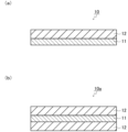
- FIG. 1(a) and (b) are cross-sectional views illustrating the configuration of a laminate according to the present disclosure.
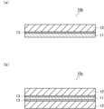
- 2(a) and (b) are cross-sectional views showing another example of the configuration of the laminate of the present disclosure.
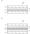
- 3(a) and (b) are cross-sectional views showing still another example of the configuration of the laminate of the present disclosure.
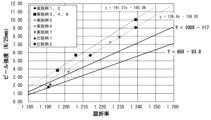
- FIG. 4 is a graph showing the relationship between peel strength and refractive index.
- the term “adhesive layer” refers to a layer formed of at least one of an adhesive and an adhesive.
- the term “adhesive layer” may be an "adhesive layer” formed of an adhesive, an “adhesive layer” formed of an adhesive, or a layer containing both an adhesive and an adhesive.
- an adhesive and an adhesive may be collectively referred to as an "adhesive”.
- an agent with relatively weak adhesive or bonding strength e.g., an agent that allows the adherend to be removed again
- an agent with relatively strong adhesive or bonding strength e.g., an agent that does not allow the adherend to be removed again or is very difficult to remove
- on or “on a surface” can mean on or in direct contact with a surface, or through another layer, etc.
- interlayer means any part that is included between one layer and another layer, including the one layer and the other layer. That is, for example, when referring to the interlayer between one layer and another layer, it may be any part of the one layer, any part of the other layer, or any part of another layer that is included between the one layer and the other layer. It may also be the boundary part between any two layers of the one layer, the other layer, and the other layer.
- the void layer of the present disclosure is a void layer to which the pulverized gel silicon compound is chemically bonded, the gel silicon compound is a compound in which a silane compound is condensed or partially condensed, the silane compound includes a monofunctional silane compound, a trifunctional silane compound, and a tetrafunctional silane compound, and the refractive index of the void layer is 1.30 or less.
- the void layer of the present disclosure is, as another embodiment, a void layer to which the pulverized gel silicon compound is chemically bonded under the coexistence condition of an additive
- the gel silicon compound is a compound in which a silane compound is condensed or partially condensed
- the additive includes at least one of a crosslinking reaction accelerator and its precursor, and a crosslinking auxiliary, the total content ratio of the crosslinking reaction accelerator and its precursor is 1.5 mol% or more, the total content ratio of the crosslinking auxiliary is 2.0 mol% or more, and the refractive index of the void layer is 1.30 or less.
- the form of use of the porous layer of the present disclosure is not particularly limited, and it can be used, for example, in the laminate of the present disclosure described above.
- the laminate of the present disclosure includes the void layer of the present disclosure and an adhesive layer, as described above.
- the adhesive layer is directly laminated to one or both sides of the void layer.
- the adhesive layer being "directly laminated" to the void layer means, for example, that the adhesive layer may be in direct contact with the void layer, or that the adhesive layer may be laminated to the void layer via the intermediate layer.
- FIG. 1(a) shows an example of the configuration of the laminate of the present disclosure.
- an adhesive layer 12 is directly laminated on one side of a void layer 11.
- the void layer 11 is a void layer to which a pulverized gel-like silicon compound is chemically bonded.
- the gel-like silicon compound is a compound in which a silane compound is condensed or partially condensed.
- the silane compound includes a monofunctional to trifunctional silane compound and a tetrafunctional silane compound, and the content ratio of the tetrafunctional silane compound to the amount of substance of the monofunctional to trifunctional silane compound is 1 to 25 mol %.
- the refractive index of the void layer 11 is 1.30 or less.
- FIG. 1(b) shows another example of the configuration of the laminate of the present disclosure.
- this laminate 10a has adhesive layers 12 laminated directly on both sides of the void layer 11.
- the laminate of the present disclosure may have an intermediate layer between the void layer and the adhesive layer, and the intermediate layer may be a layer formed by the merging of the void layer and the adhesive layer.
- FIG. 2 shows an example of such a laminate of the present disclosure.
- the laminate 10b of FIG. 2(a) has an adhesive layer 12 directly laminated on one side of the void layer 11.
- This laminate 10b is the same as the laminate 10 of FIG. 1(a) except that an intermediate layer 13 is present between the void layer 11 and the adhesive layer 12.
- the intermediate layer 13 is a layer formed by the merging of the void layer 11 and the adhesive layer 12.
- This laminate 10c is the same as the laminate 10a of FIG. 1(b) except that an intermediate layer 13 is present between the void layer 11 and each adhesive layer 12.
- the intermediate layer 13 is a layer formed by combining the void layer 11 and the adhesive layer 12.
- the laminate of the present disclosure may or may not include other components other than the void layer, the adhesive layer, and the intermediate layer.
- the other components are not particularly limited, and may be, for example, a substrate.
- the substrate is also not particularly limited, and may be, for example, a film (e.g., a resin film), a glass plate, etc., as described below.
- FIG. 3 shows an example of such a laminate of the present disclosure.
- the laminate 10d of FIG. 3(a) is the same as the laminate 10b of FIG. 2(a) except that, as shown in the figure, a substrate 14 is provided in direct contact with the surface of the void layer 11 opposite the adhesive layer 12, and on the surface of the adhesive layer 12 opposite the void layer 11.
- FIG. 3(b) is the same as the laminate 10c of FIG. 3(b) except that, as shown in the figure, a substrate 14 is provided in direct contact with the surface of the adhesive layer 12 on both sides opposite the void layer 11.
- the substrate 14 is provided on both sides of the laminate.
- the present disclosure is not limited thereto, and for example, the substrate 14 may be provided on only one side.
- the substrate 14 is provided so as to be in direct contact with the void layer 11 or the adhesive layer 12.
- the present disclosure is not limited thereto, and for example, other components may be present between the substrate 14 and the void layer 11 or the adhesive layer 12.
- the other components are not particularly limited, and may be, for example, an optical functional layer.
- the optical functional layer is also not particularly limited, and may be, for example, an optical functional layer used in a general optical film, and may be, for example, a microlens film, a prism film, a diffusion film, a polarizing reflection film, a polarizing film, a retardation film, a high refractive index layer, etc.
- the void layer of the present disclosure is a void layer in which the pulverized gel silicon compound is chemically bonded.
- the void layer is a layer in which a new pore structure (new void structure) that cannot be obtained in a layer formed from the gel silicon compound is formed, and a nanoscale void layer with high porosity can be formed.
- the void layer is, for example, a gel silicon compound
- the pulverized materials are chemically bonded to each other while adjusting the number of siloxane bond functional groups of the gel silicon compound.
- the "gel silicon compound” refers to a polymeric porous body containing siloxane bonds, and includes, for example, a porous body containing silsesquioxane as a constituent unit.
- the void layer is chemically bonded (e.g., cross-linked) in a bonding process. Therefore, when the void layer is a functional porous body, for example, the void layer has a structure with voids, but can maintain sufficient strength and flexibility. Therefore, according to the present disclosure, the void layer can be easily and simply applied to various objects.
- the form in which the pulverized materials are chemically bonded is not particularly limited, and specific examples of the chemical bond include, for example, a covalent bond, an ionic bond, and a metallic bond.
- the pulverized materials may be cross-linked (cross-linked) with each other by a covalent bond.
- the form of the chemical bond (for example, the above-mentioned cross-linking bond) of the pulverized materials may be, for example, a form in which the pulverized materials are directly bonded with each other, or a form in which the pulverized materials are indirectly bonded with each other via other substances such as a cross-linking auxiliary, a linker, or a spacer.
- the method of chemically bonding the pulverized materials is as described in the manufacturing method of the void layer described later.
- the cross-linked bond is, for example, a siloxane bond.
- the siloxane bond include the T2 bond, T3 bond, and T4 bond shown below.
- the gel silicon compound When the gel silicon compound has a siloxane bond, it may have, for example, any one type of bond, any two types of bonds, or all three types of bonds.
- the ratio of T4 among the siloxane bonds is high, the film strength will be easily expressed, but the void size will be small and the flexibility will be weak. For this reason, it is preferable to change the ratio of T2, T3, and T4 depending on the application, for example.
- the gel-like silicon compound is a compound in which a silane compound is condensed or partially condensed, as described above.
- the condensation can be, for example, dehydration condensation.
- the partially condensed state refers to a state in which, for example, some of the condensable functional groups (e.g., alkoxy groups, etc.) contained in the silane compound are condensed, and the other functional groups are not condensed and the condensable functional groups remain.
- some of the silane compounds are siloxane-bonded, and the other silane compounds are unbonded.
- the proportion of the unbonded silane compounds is, for example, less than 50%, 30% or less, or 15% or less.
- the void layer of the present disclosure includes, as the silane compound, a monofunctional silane compound and a tetrafunctional silane compound.
- the silane compound may include, for example, at least one silane compound selected from the monofunctional silane compounds and may further include a tetrafunctional silane compound.
- Examples of the monofunctional silane compound include monofunctional alkoxysilanes.
- Examples of the tetrafunctional silane compound include tetrafunctional alkoxysilanes.
- Examples of the monofunctional silane compound include trimethylmethoxysilane (TMMS), trimethylethoxysilane (TMES), trimethylpropoxysilane (TMPS), and the like.
- Examples of the bifunctional silane compound include dimethyldimethoxysilane (DDMS), dimethyldiethoxysilane (DDES), dimethyldipropoxysilane (DDPS), and the like.
- Examples of the trifunctional silane compounds include methyltrimethoxysilane (MTMS), methyltriethoxysilane (MTES), methyltrippropoxysilane (MTPS), 3-acryloxypropyltriethoxysilane, vinyltrimethoxysilane, vinyltriethoxysilane, 4-vinylbutyltrimethoxysilane, 4-vinylbutyltriethoxysilane, 8-vinyloctyltrimethoxysilane, 8-vinyloctyltriethoxysilane, 10-methacryloyloxydecyltrimethoxysilane, 10-acryloyloxydecyltrimethoxysilane, 10-methacryloyloxydecyltriethoxysilane, 10-acryl
- the content ratio of the tetrafunctional silane compound relative to the amount of substance of the mono- to trifunctional silane compound is, for example, 1 to 25 mol%.
- the lower limit of the content ratio is, for example, 2 mol% or more, 3 mol% or more, or 3.5 mol% or more
- the upper limit is, for example, 20 mol% or less, 15 mol% or less, or 10 mol% or less
- the range is, for example, 2 to 20 mol%, 3 to 15 mol%, 3.5 to 15 mol%, or 3.5 to 10 mol%.
- the content ratio is not too high from the viewpoint of ease of crushing in the gel crushing process.
- the content ratio is not too low from the viewpoint of improving the strength of the low refractive index layer.
- the void layer of the present disclosure is, for example, a void layer in which the pulverized gel silicon compound is chemically bonded in the presence of an additive.
- the additive may include, for example, at least one of a crosslinking reaction accelerator and a precursor thereof.
- the crosslinking reaction accelerator may be, for example, an acidic substance or a basic substance.
- the crosslinking reaction accelerator may be, for example, a catalyst that promotes chemical bonding (crosslinking) between the pulverized gel silicon compound.
- the precursor of the crosslinking reaction accelerator may be, for example, a substance that generates the crosslinking reaction accelerator by light or heat (crosslinking accelerator generator).
- the crosslinking reaction promoter include a photoactive catalyst and a thermally active catalyst.
- the photoactive catalyst for example, in the bonding process described below, the gel silicon compounds can be chemically bonded (for example, crosslinked) together without heating. With this, for example, in the bonding process, the crushed material to be bonded is less likely to shrink, so a higher void ratio can be maintained.
- photocatalyst generator a substance that generates a catalyst by light
- thermally active catalyst a substance that generates a catalyst by heat
- photocatalyst generator is not particularly limited, but examples thereof include photobase generators (substances that generate a basic catalyst when irradiated with light) and photoacid generators (substances that generate an acid catalyst when irradiated with light), and photobase generators are preferred.
- Examples of the photobase generator include 9-anthrylmethyl N,N-diethylcarbamate (trade name WPBG-018), (E)-1-[3-(2-hydroxyphenyl)-2-propenoyl]piperidine (trade name WPBG-027), 1-(anthraquinon-2-yl)ethyl imidazolecarboxylate (trade name WPBG-140), 2-nitrophenyl Examples include methyl 4-methacryloyloxypiperidine-1-carboxylate (trade name WPBG-165), 1,2-diisopropyl-3-[bis(dimethylamino)methylene]guanidium 2-(3-benzoylphenyl)propionate (trade name WPBG-266), 1,2-dicyclohexyl-4,4,5,5-tetramethylbiguanidium n-butyltriphenylborate (trade name WPBG-300), and 2-(9-oxoxanthen-2-yl)propionic acid 1,5
- the above-mentioned product names containing "WPBG” are all product names of Wako Pure Chemical Industries, Ltd.
- the photoacid generator include aromatic sulfonium salts (trade name SP-170: ADEKA), triarylsulfonium salts (trade name CPI101A: SAN-APRO), and aromatic iodonium salts (trade name Irgacure250: CIBA JAPAN).
- the crosslinking reaction accelerator that chemically bonds the pulverized gel silicon compound is not limited to the photoactive catalyst and the photocatalyst generator, and may be, for example, a thermally active catalyst or a thermal catalyst generator such as urea.
- crosslinking reaction accelerator that chemically bonds the pulverized gel silicon compound
- base catalysts such as potassium hydroxide, sodium hydroxide, and ammonium hydroxide
- acid catalysts such as hydrochloric acid, acetic acid, and oxalic acid.
- base catalysts are preferred.
- the crosslinking reaction accelerator and its precursor can be used by adding at least one of the crosslinking reaction accelerator and its precursor to a sol particle liquid (e.g., a suspension) containing the pulverized material (gel-like silicon compound) immediately before coating, or as a mixed liquid in which the crosslinking reaction accelerator and at least one of the precursors are mixed in a solvent.
- the mixed liquid may be, for example, a coating liquid directly added to the sol particle liquid and dissolved, a solution in which the crosslinking reaction accelerator and at least one of the precursors are dissolved in a solvent, or a dispersion in which the crosslinking reaction accelerator and at least one of the precursors are dispersed in a solvent.
- the solvent is not particularly limited, and examples thereof include water and buffer solutions.
- the amount of the crosslinking reaction accelerator and its precursor added is not particularly limited, and is, for example, 0.01 to 20% by weight, 0.05 to 10% by weight, or 0.1 to 5% by weight relative to the weight of the gel-like silicon compound.
- the lower limit of the total content ratio of the crosslinking reaction accelerator and its precursor relative to the total amount of the mono- to trifunctional silane compound and the tetrafunctional silane compound is, for example, 1 mol% or more, 1.5 mol% or more, 2 mol% or more, or 2.5 mol% or more, and the upper limit is, for example, 5 mol% or less, 4 mol% or less, 3.5 mol% or less, or 3 mol% or less.
- the lower limit of the total content ratio of the crosslinking reaction accelerator and its precursor relative to the total substance amount of the silane compounds is, for example, 1.5 mol% or more, 2 mol% or more, or 2.5 mol% or more, and the upper limit is, for example, 5 mol% or less, 4 mol% or less, 3.5 mol% or less, or 3 mol% or less.
- the additive may also include, for example, a cross-linking auxiliary.
- the cross-linking auxiliary can be considered a medium for indirectly bonding the pulverized gel silicon compound particles together by chemically bonding the pulverized gel silicon compound particles together.
- the cross-linking auxiliary penetrates between the pulverized particles, and the pulverized particles and the cross-linking auxiliary interact or bond with each other, making it possible to bond the pulverized particles together even if they are somewhat distant from each other, thereby efficiently increasing strength.
- the crosslinking auxiliary a multi-crosslinked silane monomer is preferable.
- the multi-crosslinked silane monomer has, for example, 2 to 3 alkoxysilyl groups, the chain length between the alkoxysilyl groups may be 1 to 10 carbon atoms, and may also contain elements other than carbon.
- crosslinking auxiliary examples include bis(trimethoxysilyl)ethane, bis(triethoxysilyl)ethane, bis(trimethoxysilyl)methane, bis(triethoxysilyl)methane, bis(triethoxysilyl)propane, bis(trimethoxysilyl)propane, bis(triethoxysilyl)butane, bis(trimethoxysilyl)butane, bis(triethoxysilyl)pentane, bis(trimethoxysilyl)pentane, bis(triethoxysilyl)hexane, bis(trimethoxysilyl)hexane, bis(trimethoxysilyl)-N-butyl-N-propyl-ethane-1,2-diamine, tris-(3-trimethoxysilylpropyl)isocyanurate, and tris-(3-triethoxysilylpropyl)
- the lower limit of the total content of the crosslinking auxiliary relative to the total amount of the mono- to trifunctional silane compound and the tetrafunctional silane compound is, for example, 1 mol% or more, 2 mol% or more, 2.5 mol% or more, or 3 mol% or more, and the upper limit is, for example, 6 mol% or less, 5.5 mol% or less, 5 mol% or less, 4.5 mol% or less, or 3.5 mol% or less.
- the lower limit of the total content of the crosslinking auxiliary relative to the total substance amount of the silane compounds is, for example, 2 mol% or more, or 2.5 mol% or more, and the upper limit is, for example, 6 mol% or less, 5 mol% or less, 4 mol% or less, 3.5 mol% or less, or 3 mol% or less.
- the void layer of the present disclosure has, for example, a pore structure.
- the void size of the pores in the void layer refers to the diameter of the long axis of the void (hole) among the diameters of the long axis and the short axis.
- the pore size is, for example, 5 nm to 200 nm.
- the void size is, for example, 5 nm or more, 10 nm or more, or 20 nm or more, with an upper limit of, for example, 200 nm or less, 150 nm or less, 100 nm or less, 50 nm or less, 40 nm or less, or 30 nm or less, and the range is, for example, 5 nm to 200 nm, or 10 nm to 100 nm.
- the preferred void size is determined depending on the application in which the void structure is used, and therefore, for example, it is necessary to adjust the void size to a desired void size depending on the purpose.
- the void size can be evaluated, for example, by the following method.
- the morphology of the void layer can be observed and analyzed using a scanning electron microscope (SEM).
- SEM scanning electron microscope
- the void layer is subjected to FIB processing (accelerating voltage: 30 kV) under cooling, and a cross-sectional electron image can be obtained at a magnification of 100,000 times with respect to the obtained cross-sectional sample using a FIB-SEM (manufactured by FEI: product name Helios NanoLab600, accelerating voltage: 1 kV).
- the pore size can be quantified by the BET test method. Specifically, 0.1 g of the sample (the pore layer) is placed in the capillary of a pore distribution/specific surface area measuring device (BELLSORP MINI/product name of Microtrack Bell Co., Ltd.), and then dried under reduced pressure at room temperature for 24 hours to degas the gas in the pore structure. Then, nitrogen gas is adsorbed onto the sample, and a BET plot, a BJH plot, and an adsorption isotherm are drawn to determine the pore distribution. This allows the pore size to be evaluated.
- a pore distribution/specific surface area measuring device BELLSORP MINI/product name of Microtrack Bell Co., Ltd.
- the void layer of the present disclosure may have a pore structure (porous structure) as described above, and may be, for example, an open-cell structure in which the pore structure is continuous.
- the open-cell structure means, for example, that the pore structure is three-dimensionally connected in the void layer, and can also be said to be a state in which the internal voids of the pore structure are continuous.
- the void layer forms a monolith structure in which the open-cell structure has a plurality of pore distributions.
- the monolith structure refers to, for example, a structure in which fine nano-sized voids exist, and a hierarchical structure in which the nano-voids are aggregated and exist as an open-cell structure.
- the monolith structure for example, it is possible to achieve both film strength and high porosity by imparting film strength with fine voids and high porosity with coarse open-cell voids.
- the particle size distribution of the pulverized material can be controlled to a desired size to form the monolith structure.
- the haze indicating transparency is not particularly limited, and the lower limit is, for example, 0.1% or more, 0.2% or more, or 0.3% or more, and the upper limit is, for example, 10% or less, 5% or less, or 3% or less, and the range is, for example, 0.1 to 10%, 0.2 to 5%, or 0.3 to 3%.
- the haze can be measured, for example, by the following method.
- the porous layer (porous layer of the present disclosure) is cut to a size of 50 mm x 50 mm, and is set in a haze meter (HM-150, manufactured by Murakami Color Research Laboratory Co., Ltd.) to measure the haze.
- the refractive index of a medium is generally defined as the ratio between the transmission speed of the wavefront of light in a vacuum and the propagation speed within the medium.
- the refractive index refers to the refractive index measured at a wavelength of 550 nm unless otherwise specified. There are no particular limitations on the method for measuring the refractive index, and it can be measured, for example, by the following method.
- the refractive index of the void layer of the present disclosure is 1.30 or less.
- the upper limit of the refractive index of the void layer is, for example, 1.30 or less, less than 1.30, 1.26 or less, 1.25 or less, less than 1.25, 1.24 or less, 1.23 or less, or 1.22 or less
- the lower limit is, for example, 1.05 or more, 1.10 or more, 1.15 or more, 1.16 or more, 1.17 or more, 1.18 or more, or 1.19 or more
- the range is, for example, 1.05 or more and less than 1.30, 1.05 or more and less than 1.30, 1.10 or more and less than 1.25, 1.15 or more and less than 1.25, or 1.19 or more and less than 1.25.
- the method for measuring the refractive index of the void layer is not particularly limited, and can be measured, for example, by the following method.
- the porosity of the void layer has a lower limit of, for example, 30 volume % or more, or 50 volume % or more, and an upper limit of, for example, 90 volume % or less, 75 volume % or less, or 60 volume % or less, and the range is, for example, 30 to 90 volume %, 50 to 75 volume %, or 50 to 60 volume %.
- the void remaining rate of the porous layer is, for example, at its lower limit, 10 volume% or more, 20 volume% or more, 30 volume% or more, 40 volume% or more, 50 volume% or more, 60 volume% or more, 70 volume% or more, 80 volume% or more, 85 volume% or more, or more than 85 volume%.
- the method for measuring the refractive index of the porous layer is not particularly limited, and can be measured, for example, by the following method.
- the laminate thus produced is placed in an oven at a temperature of 85° C. and a humidity of 85% RH, and a heat and humidity durability test is carried out for 500 hours.
- the degree to which the voids in the porous layer are filled after the heat and humidity durability test is confirmed by SEM, and the remaining porosity can be calculated.
- the shape of the void layer of the present disclosure is not particularly limited, and may be, for example, a film shape or a block shape, etc.
- the method for producing the void layer of the present disclosure is not particularly limited, but may be, for example, the method for producing a void layer described below, or the method described in WO 2019/065999 and WO 2019/065803. The descriptions in these publications are incorporated herein by reference.
- the adhesive layer is not particularly limited.
- the adhesive or the adhesive forming the adhesive layer is not particularly limited, and for example, a general adhesive or adhesive can be used.
- the adhesive or the adhesive include polymer adhesives such as acrylic, vinyl alcohol, silicone, polyester, polyurethane, polyether, and rubber adhesives.
- examples also include adhesives composed of water-soluble crosslinking agents of vinyl alcohol polymers such as glutaraldehyde, melamine, and oxalic acid. These adhesives and adhesives may be used alone or in combination (for example, mixed, laminated, etc.).
- the thickness of the adhesive layer is not particularly limited, and may be, for example, 0.1 to 100 ⁇ m, 5 to 50 ⁇ m, 10 to 30 ⁇ m, or 12 to 25 ⁇ m.
- Nanoindentation hardness evaluation A measurement sample is cut into a size of about 1 cm square and fixed to a predetermined support, and the nanoindentation hardness of the adhesive layer in the laminate of the present disclosure is measured under the following conditions.
- the nanoindentation hardness can be measured by a nanoindentation method.
- ⁇ Analyzer Hysitron Inc.
- Triboindenter ⁇ Used indenter: Conical (spherical: diameter 20 ⁇ m) Measurement method: Single indentation measurement Measurement temperature: Room temperature Indentation depth: 2000 nm
- Nanoindentation hardness Pmax/A
- the nanoindentation hardness may be the nanoindentation hardness of either the surface of the adhesive layer or the cross section of the adhesive layer.
- the interlayer peel strength between the void layer and the adhesive layer measured at a tensile speed of 0.3 m/min using a tensile tester is, for example, 3 N/25 mm or more.
- the lower limit of the peel strength may be, for example, 3.5 N/25 mm or more, 4.0 N/25 mm or more, or 5.0 N/25 mm or more.
- the upper limit of the peel strength is not particularly limited, but is, for example, 20 N/25 mm or less, 15 N/25 mm or less, or 10 N/25 mm or less.
- the peel strength is, for example, a peel strength measured due to cohesive failure of the void layer.
- the method for measuring the peel strength is not particularly limited, and can be measured, for example, by the following method.
- a resin film substrate having a void layer (void layer of the present disclosure) and a tacky adhesive layer (tacky adhesive layer in the laminate of the present disclosure) formed thereon is prepared, and an acrylic adhesive layer (thickness 20 ⁇ m) is bonded to the opposite side of the void layer in the resin film substrate.
- the bonded sample is cut to 50 mm x 25 mm to prepare an adhesive tape piece.
- the tacky adhesive layer (thickness 10 ⁇ m) on the void layer side is bonded to a PET film (T100: manufactured by Mitsubishi Plastics Film Co., Ltd.) cut into a strip of 25 mm x 100 mm, and the acrylic adhesive layer on the resin film substrate side is laminated and fixed with glass.
- a tensile tester manufactured by Shimadzu Corporation, product name: Autograph (registered trademark) AG-Xplus
- the refractive index of the void layer of the present disclosure measured in the laminate state is, for example, 1.30 or less.
- the upper limit of the refractive index of the void layer measured in the laminate state is, for example, 1.30 or less, less than 1.30, 1.26 or less, 1.25 or less, less than 1.25, 1.24 or less, 1.23 or less, or 1.22 or less
- the lower limit is, for example, 1.05 or more, 1.10 or more, 1.15 or more, 1.16 or more, 1.17 or more, 1.18 or more, or 1.19 or more
- the range is, for example, 1.05 or more and less than 1.30, 1.05 or more and less than 1.30, 1.10 or more and less than 1.25, 1.15 or more and less than 1.25, or 1.19 or more and less than 1.25.
- the method for measuring the refractive index of the void layer of the present disclosure measured in the laminate state is not particularly limited, and can be measured, for example, by the following method.
- the laminate of the present disclosure may satisfy the following condition (2), for example, when the refractive index is X and the peel strength is Y.
- Fig. 4 shows a graph showing the relationship between the peel strength and the refractive index under condition (1).
- Condition (2) Y ⁇ 100X-117
- condition (1) or the condition (2) for example, a laminate having a low refractive index and high peel strength (i.e., excellent mechanical strength) can be obtained.
- the type, content ratio, etc. of the tetrafunctional silane compound and the additive may be appropriately adjusted, although there is no particular limitation thereto.
- the intermediate layer is not particularly limited, but for example, as described above, is a layer formed by merging a part of the void layer with a part of the adhesive layer.
- the thickness of the intermediate layer is not particularly limited, but for example, is 1 to 1500 nm, 5 to 1000 nm, 10 to 800 nm, or 20 to 500 nm.
- the form of the laminate disclosed herein is not particularly limited, but is typically in the form of a film.
- the laminate of the present disclosure is, for example, a roll body.
- the laminate of the present disclosure may further include a resin film, for example, as described above, and the void layer may be formed on the long resin film.
- another long film may be laminated on the laminate of the present disclosure, or another long resin film (for example, an interleaf paper, a release film, a surface protection film, etc.) may be laminated on the laminate of the present disclosure including the resin film and the void layer, and then wound into a roll body.
- the method for producing the laminate of the present disclosure is not particularly limited, but it can be produced, for example, by the production method of the present disclosure shown below.
- the method for producing the optical laminate of the present disclosure that does not contain a resin film can be performed in the same manner as the production method of the laminate of the present disclosure, except that no resin film is used, unless otherwise specified.
- the method for producing the void layer and the laminate of the present disclosure is not particularly limited, and may be, for example, the production method described below. However, the following description is merely an example and does not limit the present disclosure in any way.
- the method for producing a laminate including a void layer according to the present disclosure includes, for example, a void layer forming step of forming the void layer, and an adhesive layer forming step of forming the adhesive layer on the void layer.
- the method for producing the laminate may further include an intermediate layer forming step of reacting the void layer with the adhesive layer to form the intermediate layer.
- the void layer forming process includes a gel silica synthesis process, a gel crushing process, and a bonding process, as described above.
- the void layer forming process may or may not include other processes in addition to the gel silica synthesis process, the gel crushing process, and the bonding process.
- the other processes are not particularly limited, but include, for example, a coating process and a drying process, which will be described later.
- the gel silica synthesis process includes a process of synthesizing a gel silicon compound by condensing or partially condensing the silane compound.
- the gel silica synthesis process may include, for example, a process of gelling a block of porous material in a solvent to form a gel.
- the gel gelled by the gel silica synthesis process is used in the first grinding stage (for example, the first grinding stage described below) of multiple grinding stages described below.
- the method for manufacturing the void layer includes, for example, an aging step in which the gelled gel is aged in a solvent.
- the gel after the aging step is used in the first crushing step (e.g., the first crushing step) of the multiple crushing steps.
- the gel crushing step includes a step of crushing the gel-like silicon compound to obtain a crushed product.
- the gel crushing step may be a single step, but is preferably divided into multiple crushing steps.
- the number of crushing steps is not particularly limited, and may be, for example, two steps or three or more steps.
- the volume average particle diameter of the gel after the first crushing step may be, for example, 0.5 to 100 ⁇ m, 1 to 100 ⁇ m, 1 to 50 ⁇ m, 2 to 20 ⁇ m, or 3 to 10 ⁇ m.
- the volume average particle diameter of the gel after the second crushing step may be, for example, 10 to 1000 nm, 100 to 500 nm, or 200 to 300 nm.
- the volume average particle diameter indicates the particle size variation of the crushed material in the liquid containing the gel (gel-containing liquid).
- the volume average particle diameter can be measured, for example, by a particle size distribution evaluation device such as a dynamic light scattering method or a laser diffraction method, and an electron microscope such as a scanning electron microscope (SEM) or a transmission electron microscope (TEM).
- SEM scanning electron microscope
- TEM transmission electron microscope
- the solvent replacement step is performed to replace the solvent with another solvent.
- the gel in the other solvent is used in the first crushing step (e.g., the first crushing step) of the multiple crushing steps.
- the grinding of the porous body is controlled, for example, while measuring the shear viscosity of the liquid.
- At least one of the multiple grinding stages (e.g., at least one of the first grinding stage and the second grinding stage) of the method for producing a porous layer disclosed herein is carried out, for example, by high-pressure media-less grinding.
- gel powder-containing liquid obtained by a process including the gel crushing process may be simply referred to as "gel powder-containing liquid.”
- the gel powder-containing liquid can form the void layer as a functional porous body, for example, by forming a coating film and chemically bonding the pulverized material in the coating film through a bonding process.
- the gel powder-containing liquid can provide the void layer on various objects, for example. Therefore, the gel powder-containing liquid and the manufacturing method thereof are useful, for example, in manufacturing the void layer.
- the liquid containing the crushed gel has, for example, extremely excellent uniformity, so that when the void layer is used for applications such as optical components, the appearance can be improved.
- the gel powder-containing liquid may be, for example, a gel powder-containing liquid that is applied (coated) onto a substrate (application step) and then dried (drying step) to obtain a layer having a high porosity (porous layer).
- the coating method of the gel powder-containing liquid is not particularly limited, and a general coating method can be adopted.
- the coating method include the slot die method, reverse gravure coating method, microgravure method (microgravure coating method), dip method (dip coating method), spin coating method, brush coating method, roll coating method, flexographic printing method, wire bar coating method, spray coating method, extrusion coating method, curtain coating method, and reverse coating method.
- the extrusion coating method, curtain coating method, roll coating method, and microgravure coating method are preferred.
- the coating amount of the gel powder-containing liquid is not particularly limited, and can be appropriately set, for example, so that the thickness of the void layer is appropriate.
- the thickness of the void layer is not particularly limited, and is, for example, as described above.
- the gel powder-containing liquid is dried (i.e., the dispersion medium contained in the gel powder-containing liquid is removed) to form the coating film (precursor of the void layer) after drying.
- the temperature of the drying process in the drying step is, for example, 50 to 250°C, 60 to 150°C, or 70 to 130°C, and the drying time is, for example, 0.1 to 30 minutes, 0.2 to 10 minutes, or 0.3 to 3 minutes.
- the drying temperature and time are preferably lower and shorter in terms of, for example, continuous productivity and the development of a high porosity.
- the substrate may expand in the drying oven as the substrate approaches the glass transition temperature of the substrate, and defects such as cracks may occur in the formed void structure immediately after coating.
- the conditions are too lenient, for example, in roll-to-roll processing, residual solvent may be contained at the time of leaving the drying oven, and when rubbed against the roll in the next process, defects in appearance such as scratches may occur.
- the drying method may be, for example, natural drying, heat drying, or reduced pressure drying.
- the drying method is not particularly limited, and for example, a general heating means may be used.
- the heating means include a hot air blower, a heating roll, and a far-infrared heater. Among these, when continuous industrial production is assumed, it is preferable to use heat drying.
- the bonding step includes a step of chemically bonding the pulverized material.
- the bonding step can be performed, for example, by irradiating the coating film containing a catalyst or catalyst generator that has been added in advance to the gel pulverized material-containing liquid with light or by heating, or by spraying the catalyst onto the coating film and then irradiating it with light or by heating, or by irradiating it with light or by heating while spraying the catalyst or catalyst generator.
- the catalyst may be, for example, the crosslinking reaction accelerator, or may be a strength enhancer that improves the strength of the void layer, or the crosslinking accelerator may also function as the strength enhancer.
- the integrated light amount of the light irradiation is not particularly limited, but is, for example, 200 to 800 mJ/cm 2 , 250 to 600 mJ/cm 2 , or 300 to 400 mJ/cm 2 calculated at 360 nm. From the viewpoint of preventing an insufficient amount of irradiation resulting in insufficient effect due to insufficient decomposition of the catalyst generator caused by light absorption, an integrated light amount of 200 mJ/cm 2 or more is preferable. Moreover, from the viewpoint of preventing damage to the substrate under the void layer and the occurrence of thermal wrinkles, an integrated light amount of 800 mJ/cm 2 or less is preferable.
- the heating temperature and heating time in the heating are not particularly limited, and the conditions of the heat treatment are not particularly limited.
- the heating temperature is, for example, 50 to 250°C, 60 to 150°C, or 70 to 130°C, and the heating time is, for example, 0.1 to 30 minutes, 0.2 to 10 minutes, or 0.3 to 3 minutes.
- the step of drying the applied gel powder-containing liquid as described above may also serve as a step of carrying out a chemical reaction in the presence of the catalyst. That is, in the step of drying the applied gel powder-containing liquid (e.g., a suspension), the pulverized materials may be chemically bonded to each other by a chemical reaction in the presence of the catalyst.
- the pulverized materials may be further bonded to each other by further heating the coating film after the drying step.
- the chemical reaction in the presence of the catalyst may also occur in the step of preparing the microporous particle-containing liquid (e.g., a suspension) and the step of applying the microporous particle-containing liquid.
- this assumption does not limit the present disclosure in any way.
- the adhesive layer forming step may include, for example, an adhesive coating liquid application step of applying the adhesive coating liquid to a substrate, and a heat drying step of heating and drying the substrate coated with the adhesive coating liquid.
- the adhesive layer side of an adhesive tape or the like having the adhesive layer laminated on a substrate may be attached to the void layer to form the adhesive layer on the void layer.
- the substrate such as the adhesive tape may be left attached as it is, or may be peeled off from the adhesive layer.
- the adhesive layer may be manufactured using the adhesive coating liquid, for example, as described above.
- the adhesive layer forming step can be carried out, for example, as follows.
- the adhesive coating liquid is produced by a mixing step of mixing all the components of the adhesive coating liquid.
- the adhesive coating liquid may contain, for example, a (meth)acrylic polymer, and may or may not further contain a crosslinking agent (for example, an isocyanate-based crosslinking agent or an epoxy-based crosslinking agent).
- the adhesive coating liquid may contain, for example, the (meth)acrylic polymer, a monomer having one or two reactive double bonds in one molecule, a crosslinking agent, and an organic peroxide. In this case, if the adhesive coating liquid contains other components, the other components may also be mixed together.
- the polymerization solvent used in producing the (meth)acrylic polymer may be mixed as it is as a component of the adhesive coating liquid without removing it.
- the method for producing the adhesive coating liquid may or may not include other steps other than the mixing step, and may simply mix all the components of the adhesive coating liquid by the mixing step.
- the substrate is not particularly limited and may be, for example, a substrate such as a film.
- the substrate may preferably be, for example, a substrate made of a thermoplastic resin, a substrate made of glass, an inorganic substrate such as silicon, a plastic molded from a thermosetting resin, an element such as a semiconductor, or a carbon fiber-based material such as a carbon nanotube, but is not limited thereto.
- the substrate may be in the form of, for example, a film or a plate.
- thermoplastic resin examples include polyethylene terephthalate (PET), acrylic, cellulose acetate propionate (CAP), cycloolefin polymer (COP), triacetyl cellulose (TAC), polyethylene naphthalate (PEN), polyethylene (PE), polypropylene (PP), etc.
- PET polyethylene terephthalate
- CAP cellulose acetate propionate
- COP cycloolefin polymer
- TAC triacetyl cellulose
- PEN polyethylene naphthalate
- PE polypropylene
- the thickness of the adhesive coating liquid is not particularly limited, but may be appropriately adjusted so that the adhesive layer after drying has a predetermined thickness.
- the thickness of the adhesive layer after drying is also not particularly limited, but may be, for example, as described below.
- the substrate coated with the adhesive coating liquid is heated and dried (heat drying process).
- the temperature of the heat drying is not particularly limited, but may be, for example, 50°C or more, 80°C or more, 100°C or more, or 155°C or more, and may be, for example, 200°C or less, 180°C or less, or 160°C or less.
- the time of the heat drying is not particularly limited, but may be, for example, 0.5 minutes or more, 1 minute or more, or 3 minutes or more, and may be, for example, 60 minutes or less, 30 minutes or less, 20 minutes or less, or 10 minutes or less.
- the adhesive layer and the void layer are bonded together (bonding step).
- This method is not particularly limited, but for example, as described above, the adhesive layer side of an adhesive tape or the like in which the adhesive layer of the present disclosure is laminated on a substrate may be bonded onto the void layer to form the adhesive layer on the void layer. In this manner, the laminate of the present disclosure can be manufactured.
- the thickness of the adhesive layer is not particularly limited, but is, for example, 0.1 to 100 ⁇ m, 5 to 50 ⁇ m, 10 to 30 ⁇ m, or 12 to 25 ⁇ m.
- a heating step may be further performed in which the adhesive layer and the void layer are heated after the lamination step.
- this heating step may be referred to as an "aging step".
- the heating temperature is not particularly limited, but may be, for example, 40°C or higher, 45°C or higher, or 50°C or higher, and may be, for example, 80°C or lower, 70°C or lower, 60°C or lower, or 55°C or lower.
- the heating time is not particularly limited, but may be, for example, 1 minute or more, 10 minutes or more, 60 minutes or more, or 1800 minutes or more, and may be, for example, 3000 minutes or less, 2800 minutes or less, 2500 minutes or less, or 2000 minutes or less.
- the intermediate layer is formed by the merging of the void layer and the adhesive layer.
- the intermediate layer serves as a stopper, and the voids in the void layer are filled with the adhesive, thereby suppressing a decrease in the porosity.
- the fusion of the void layer and the adhesive layer may be such that the adhesive layer is embedded in the voids of the void layer and chemically bonded to it, or the adhesive layer may be embedded in the voids of the void layer.
- the adhesive layer can protect the void layer from physical damage (particularly scratches).
- the adhesive layer is preferably, but not limited to, one with excellent pressure resistance so that the void layer is not crushed even in a void layer-containing adhesive sheet that does not have a substrate (substrate-less).
- the laminate of the present disclosure thus obtained may be, for example, further laminated with another film (layer) as described above to form a laminate structure including the void layer (porous structure).
- each component in the laminate structure, may be laminated, for example, via the adhesive layer (adhesive or adhesive).
- the lamination of each of the above components may be performed, for example, by continuous processing using a long film (such as roll-to-roll processing) for efficiency, or, if the substrate is a molded product, element, etc., batch processing may be performed before lamination.
- a long film such as roll-to-roll processing
- batch processing may be performed before lamination.
- the optical member of the present disclosure includes the void layer of the present disclosure or the laminate of the present disclosure.
- the optical member of the present disclosure is characterized by including the void layer of the present disclosure or the laminate of the present disclosure, and other configurations are not limited in any way.
- the optical member of the present disclosure may further include other layers in addition to the void layer or the laminate.
- the optical member of the present disclosure is, for example, in a roll form.
- the optical device of the present disclosure includes the optical member of the present disclosure.
- the optical device of the present disclosure is not particularly limited, and may be, for example, an image display device or a lighting device.
- the image display device include a liquid crystal display, an organic EL (Electro Luminescence) display, and a micro LED (Light Emitting Diode) display.
- the lighting device include organic EL lighting.
- the number of parts (relative amount used) of each substance is in parts by mass (parts by weight) unless otherwise specified.
- an adhesive adheresive composition
- “adhesive layer” corresponds to "adhesive layer”.
- “adhesive layer” and “adhesive layer” are synonymous unless otherwise specified.
- the nanoindentation hardness, the refractive index of the void layer measured in the laminate state (Refractive Index (Laminate)), and the refractive index when only the void layer is measured (Refractive Index (Void Layer)), peel strength, and void remaining rate were each measured by the methods described in the embodiments.
- acrylic pressure-sensitive adhesive composition (acrylic pressure-sensitive adhesive solution) was prepared by blending 0.2 parts of an isocyanate crosslinking agent (trade name "Coronate L” manufactured by Nippon Polyurethane Industry Co., Ltd., an adduct of trimethylolpropane and tolylene diisocyanate), 0.3 parts of benzoyl peroxide (trade name "Niper BMT” manufactured by Nippon Oil & Fats Corporation), and 0.1 parts of ⁇ -glycidoxypropylmethoxysilane (trade name "KBM-403" manufactured by Shin-Etsu Chemical Co., Ltd.) with 100 parts of the solid content of the acrylic polymer solution obtained in (1) above.
- an isocyanate crosslinking agent trade name "Coronate L” manufactured by Nippon Polyurethane Industry Co., Ltd., an adduct of trimethylolpropane and tolylene diisocyanate
- benzoyl peroxide trade name "Niper BMT” manufactured by
- (meth)acrylic polymer (A1) solution A monomer mixture containing 79.5 parts of butyl acrylate, 15 parts of N-acryloylmorpholine, 5 parts of acrylic acid, and 0.5 parts of 4-hydroxybutyl acrylate was charged into a four-neck flask equipped with a stirring blade, a thermometer, a nitrogen gas inlet tube, and a cooler. Furthermore, 0.1 parts of 2,2'-azobisisobutyronitrile as a polymerization initiator was charged together with 70 parts of ethyl acetate with respect to 100 parts of the monomer mixture, and nitrogen gas was introduced while gently stirring to replace the atmosphere with nitrogen.
- (meth)acrylic pressure-sensitive adhesive composition 0.2 parts of an isocyanate crosslinking agent (trade name "Coronate L” manufactured by Nippon Polyurethane Industry Co., Ltd., an adduct of trimethylolpropane and tolylene diisocyanate) and 0.2 parts of an epoxy crosslinking agent 1,3-bis(N,N-diglycidylaminomethyl)cyclohexane (trade name "Tetrad C” manufactured by Mitsubishi Gas Chemical Company, Inc.) were blended with 100 parts of the solid content of the obtained solution of the (meth)acrylic polymer (A1) to prepare a solution of an acrylic pressure-sensitive adhesive composition.
- an isocyanate crosslinking agent trade name "Coronate L” manufactured by Nippon Polyurethane Industry Co., Ltd., an adduct of trimethylolpropane and tolylene diisocyanate
- a solution of an acrylic pressure-sensitive adhesive composition was prepared by blending 0.1 parts of an isocyanate crosslinking agent (manufactured by Mitsui Takeda Chemical Co., Ltd. under the trade name "Takenate D110N", trimethylolpropane xylylene diisocyanate), 0.1 parts of benzoyl peroxide (manufactured by Nippon Oil & Fats Co., Ltd. under the trade name "Niper BMT”), and 0.2 parts of ⁇ -glycidoxypropyl methoxysilane (manufactured by Shin-Etsu Chemical Co., Ltd. under the trade name "KBM-403”) with 100 parts of the solid content of the acrylic polymer solution obtained in (1) above.
- an isocyanate crosslinking agent manufactured by Mitsui Takeda Chemical Co., Ltd. under the trade name "Takenate D110N", trimethylolpropane xylylene diisocyanate
- benzoyl peroxide manufactured
- Laminates including a void layer in Examples 1 to 8 and Comparative Examples 1 to 3 were produced by the following method.
- Example 1 Gelation of silicon compound (gel silica synthesis process) 1.90 g of methyltrimethoxysilane (MTMS) and 0.1 g of tetraethoxysilane (TEOS), which are precursors of silicon compounds, were dissolved in 4.4 g of dimethyl sulfoxide (DMSO) to prepare a mixed solution A. 1.0 g of 0.01 mol/L oxalic acid solution was added to this mixed solution A, and MTMS was hydrolyzed by stirring at room temperature for 30 minutes to produce a mixed solution B containing tris(hydroxy)methylsilane and tetra(hydroxy)silane.
- DMSO dimethyl sulfoxide
- the crushing process (high-pressure media-less crushing) was performed using a homogenizer (manufactured by SMT Co., Ltd., product name "UH-50"), and 1.85 g of the gel-like compound and 1.15 g of IPA in the mixed liquid D were weighed into a 5 cc screw bottle, and then crushed for 2 minutes under the conditions of 50 W and 20 kHz.
- a homogenizer manufactured by SMT Co., Ltd., product name "UH-50”
- the gel-like silicon compound in the mixed liquid D was pulverized by this pulverization process, and the mixed liquid D became a pulverized sol liquid E.
- the volume average particle size which indicates the particle size variation of the pulverized material contained in the sol liquid E, was confirmed to be 0.50 to 0.70 ⁇ m using a dynamic light scattering nanotrack particle size analyzer (manufactured by Nikkiso Co., Ltd., UPA-EX150 type) and was found to be 0.50 to 0.70 ⁇ m.
- a 1.5 wt % MEK (methyl ethyl ketone) solution of a photobase generator (product name: WPBG266, Wako Pure Chemical Industries, Ltd.), which is a precursor of a crosslinking reaction accelerator, and 0.036 g of a 5% MEK solution of a crosslinking auxiliary (bis(trimethoxysilyl)hexane) were added to 0.75 g of the sol liquid E to obtain a coating liquid for forming a low refractive index layer.
- the coating liquid for forming the low refractive index layer was applied to an acrylic substrate and dried to form a void layer with a thickness of about 850 nm (void ratio 59% by volume).
- the coating was performed using a wire bar, and the drying temperature and drying time were 100°C and 2 minutes, respectively.
- UV irradiation 300 mJ was performed from the void layer surface to bond the pulverized gel compound together (bonding process).
- the bonding between the pulverized gel compound in the bonding process includes at least one of cross-linking (covalent bond) in which the pulverized gel compounds are directly bonded to each other without the aid of a cross-linking auxiliary, and cross-linking (covalent bond) via the aid of the cross-linking auxiliary.
- a 10 ⁇ m thick adhesive 1 was attached to the void layer surface, and aged at 50°C for 30 hours to produce the void layer of this example.
- the laminate of this example was also produced using the produced void layer.
- Example 2 The porous layer of this example was produced by carrying out the same operation as in Example 1, except that the amounts of the photobase generator and crosslinking auxiliary added in Example 1 were changed to 0.186 g of a 1.5 wt % MEK (methyl ethyl ketone) solution of a photobase generator (Wako Pure Chemical Industries, Ltd., product name: WPBG266) and 0.054 g of a 5% MEK solution of a crosslinking auxiliary (1,6-bis(trimethoxysilyl)hexane) per 0.75 g of sol solution E.
- the produced porous layer was used to produce a laminate of this example.
- Example 3 The air gap layer of this example was manufactured by the same procedure as in Example 1, except that the amount of tetraethoxysilane (TEOS) added in Example 1 was changed to 0.2 g.
- the laminate of this example was manufactured by using the manufactured air gap layer.
- Example 4 The air gap layer of this example was manufactured by the same procedure as in Example 2, except that the amount of tetraethoxysilane (TEOS) added in Example 1 was changed to 0.2 g.
- the laminate of this example was manufactured by using the manufactured air gap layer.
- Example 5 The air gap layer of this example was produced by carrying out the same operation as in Example 1, except that the adhesive 2 was used instead of the adhesive 1 used in Example 1. In addition, the produced air gap layer was used to produce the laminate of this example.
- Example 6 The air gap layer of this example was manufactured by the same procedure as in Example 1, except that the amount of tetraethoxysilane (TEOS) added in Example 1 was changed to 0.3 g.
- the laminate of this example was manufactured by using the manufactured air gap layer.
- Example 7 The air gap layer of this example was manufactured by the same procedure as in Example 1, except that the amount of tetraethoxysilane (TEOS) added in Example 1 was changed to 0.4 g. In addition, the laminate of this example was manufactured by using the manufactured air gap layer.
- TEOS tetraethoxysilane
- Example 8 The amount of tetraethoxysilane (TEOS) added in Example 1 was changed to 0.2 g, and the amount of the photobase generator and the bis-crosslinking accelerator added was changed to 0.062 g of a 1.5 wt % concentration MEK (methyl ethyl ketone) solution of the photobase generator (Wako Pure Chemical Industries, Ltd., product name: WPBG266) and 0.018 g of a 5% concentration MEK solution of the bis-crosslinking accelerator ((trimethoxysilyl)hexane) per 0.75 g of sol solution E, except that the operation was the same as in Example 1 to produce the void layer of this example. In addition, the laminate of this example was produced using the produced void layer.
- MEK methyl ethyl ketone
- Comparative Example 1 The air gap layer of this comparative example was produced in the same manner as in Example 9, except that tetraethoxysilane (TEOS) was not added. The produced air gap layer was used to produce a laminate of this comparative example.
- TEOS tetraethoxysilane
- Comparative Example 2 The void layer of this comparative example was produced by carrying out the same operation as in Comparative Example 1, except that the adhesive 2 was used instead of the adhesive 1 used in Comparative Example 1. In addition, the produced void layer was used to produce the laminate of this example.
- Comparative Example 3 The void layer of this comparative example was produced in the same manner as in Comparative Example 1, except that the adhesive 3 was used instead of the adhesive 1 used in Comparative Example 1. In addition, the produced void layer was used to produce the laminate of this comparative example.
- the laminates including the void layer of the examples had good interlayer peel strengths of 3 N/25 mm or more.
- the laminates of the comparative examples all had interlayer peel strengths of less than 3 N/25 mm.
- Figure 4 shows a graph showing the relationship between peel strength and refractive index for examples and comparative examples in which the nanoindentation hardness is 0.5 MPa or more when laminated.
- the peel strength between the void layer and the adhesive layer was 3N/25mm or more.
- the void layers of all examples satisfied the condition (1) (Y ⁇ 80X-93.8) described in the embodiment.
- the void layers of the examples which contain a tetrafunctional silane compound as a silane compound, have a higher peel strength than void layers having the same refractive index but not containing a tetrafunctional silane compound.
- the condition (2) (Y ⁇ 100X-117) described in the embodiment was satisfied.
- the peel strength was further improved.
- the void layer is a void layer in which pulverized gel silicon compound is chemically bonded,
- the gel silicon compound is a compound in which a silane compound is condensed or partially condensed,
- the silane compound includes a monofunctional to trifunctional silane compound and a tetrafunctional silane compound,
- the refractive index of the gap layer is 1.30 or less.
- Void layer (Appendix 2)
- the content ratio of the tetrafunctional silane compound to the amount of the monofunctional to trifunctional silane compound is 1 to 25 mol %. 2.
- the void layer is a void layer in which the pulverized gel silicon compound is chemically bonded in the presence of an additive,
- the additive includes at least one of a crosslinking reaction accelerator and a precursor thereof,
- the precursor is a substance that generates the crosslinking reaction accelerator by the action of light or heat.
- the air gap layer according to claim 3, wherein the crosslinking reaction accelerator is an acidic substance or a basic substance.
- (Appendix 5) 5.
- the air gap layer according to claim 3 or 4 wherein the total content of the crosslinking reaction accelerator and its precursor is 1 mol % or more relative to the total amount of the mono- to trifunctional silane compound and the tetrafunctional silane compound.
- the void layer is a void layer in which the pulverized gel silicon compound is chemically bonded in the presence of an additive,
- the additive includes a crosslinking auxiliary.
- the void layer according to any one of claims 1 to 5.
- the void layer is a void layer in which pulverized gel silicon compound is chemically bonded in the presence of an additive,
- the gel silicon compound is a compound in which a silane compound is condensed or partially condensed,
- the additives include at least one of a crosslinking reaction accelerator and a precursor thereof, and a crosslinking auxiliary; Relative to the total amount of the silane compounds,
- the total content of the crosslinking reaction accelerator and its precursor is 1.5 mol% or more
- the total content of the crosslinking auxiliary is 2.0 mol% or more
- the refractive index of the gap layer is 1.30 or less. Void layer.
- the method includes a gel silica synthesis step, a gel crushing step, and a bonding step
- the gel silica synthesis step includes a step of synthesizing a gel silicon compound by condensing or partially condensing a silane compound
- the silane compound includes a monofunctional to trifunctional silane compound and a tetrafunctional silane compound
- the gel crushing step includes a step of crushing the gel silicon compound to obtain a crushed product
- the bonding step includes a step of chemically bonding the pulverized material.
- a method for producing a gap layer comprising the steps of:
- the method includes a gel silica synthesis step, a gel crushing step, and a bonding step
- the gel silica synthesis step includes a step of synthesizing a gel silicon compound by condensing or partially condensing a silane compound
- the gel crushing step includes a step of crushing the gel silicon compound to obtain a crushed product
- the bonding step includes a step of chemically bonding the pulverized material in the presence of an additive
- the additives include at least one of a crosslinking reaction accelerator and a precursor thereof, and a crosslinking auxiliary.
- the present disclosure can provide a void layer having a low refractive index and excellent mechanical strength, a method for manufacturing a void layer, a laminate, an optical member, and an optical device.
- the applications of the present disclosure are not particularly limited.
- the optical device of the present disclosure is not particularly limited, and examples thereof include image display devices and lighting devices. Examples of the image display devices include liquid crystal displays, organic EL displays, and micro LED displays. Examples of the lighting devices include organic EL lighting.
- the applications of the laminate of the present disclosure are not limited to the optical members and optical devices of the present disclosure, and are arbitrary, and can be used for a wide range of applications.
Landscapes
- Physics & Mathematics (AREA)
- Chemical & Material Sciences (AREA)
- Optics & Photonics (AREA)
- General Physics & Mathematics (AREA)
- Organic Chemistry (AREA)
- Medicinal Chemistry (AREA)
- Polymers & Plastics (AREA)
- Health & Medical Sciences (AREA)
- Chemical Kinetics & Catalysis (AREA)
- Engineering & Computer Science (AREA)
- Materials Engineering (AREA)
- Composite Materials (AREA)
- Laminated Bodies (AREA)
- Silicon Polymers (AREA)
- Surface Treatment Of Optical Elements (AREA)
- Manufacture Of Porous Articles, And Recovery And Treatment Of Waste Products (AREA)
- Optical Elements Other Than Lenses (AREA)
- Electroluminescent Light Sources (AREA)
- Joining Of Glass To Other Materials (AREA)
- Pigments, Carbon Blacks, Or Wood Stains (AREA)
- Paints Or Removers (AREA)
Abstract
低屈折率であり、かつ、機械的強度に優れた空隙層を提供する。 本開示の空隙層(11)は、ゲル状ケイ素化合物の粉砕物が化学的に結合している空隙層であり、前記ゲル状ケイ素化合物は、シラン化合物が縮合又は部分的に縮合した化合物であり、前記シラン化合物として、1~3官能シラン化合物及び4官能シラン化合物を含み、空隙層(11)の屈折率が、1.30以下である。
Description
本開示は、空隙層、空隙層の製造方法、積層体、光学部材、及び光学装置に関する。
光学デバイスにおいては、例えば、全反射層として、低屈折率層を用いることが提案されている。例えば、特許文献1では、導光板と反射板との間に導光板よりも低屈折率である層を挿入した積層体が開示されている。低屈折率層としては、例えば、屈折率をなるべく空気に近い低屈折率とするために、空隙を有する空隙層が用いられる。
前述のとおり、空隙層は空隙を有する層である。一般的に、空隙層の屈折率は、空隙層の空隙率を高くするほど、低屈折率となる傾向にある。一方で、空隙層の空隙率を高くした場合、空隙層は機械的強度が低くなる傾向にある。すなわち、空隙層の屈折率と空隙層の機械的強度はトレードオフの関係にある。したがって、低屈折率であっても機械的強度の高い空隙層の実現が望まれる。
そこで、本開示は、低屈折率であり、かつ、機械的強度に優れた空隙層、空隙層の製造方法、積層体、光学部材、及び光学装置の提供を目的とする。
前記目的を達成するために、本開示の空隙層は、
ゲル状ケイ素化合物の粉砕物が化学的に結合している空隙層であり、
前記ゲル状ケイ素化合物は、シラン化合物が縮合又は部分的に縮合した化合物であり、
前記シラン化合物として、1~3官能シラン化合物及び4官能シラン化合物を含み、
前記空隙層の屈折率が、1.30以下である。
ゲル状ケイ素化合物の粉砕物が化学的に結合している空隙層であり、
前記ゲル状ケイ素化合物は、シラン化合物が縮合又は部分的に縮合した化合物であり、
前記シラン化合物として、1~3官能シラン化合物及び4官能シラン化合物を含み、
前記空隙層の屈折率が、1.30以下である。
本開示の空隙層は、
添加剤の共存条件においてゲル状ケイ素化合物の粉砕物が化学的に結合している空隙層であり、
前記ゲル状ケイ素化合物は、シラン化合物が縮合又は部分的に縮合した化合物であり、
前記添加剤として、架橋反応促進剤及びその前駆体の少なくとも一方、並びに架橋補助剤を含み、
前記シラン化合物の合計の物質量に対して、
前記架橋反応促進剤及びその前駆体の合計含有割合が、1.5mol%以上であり、
前記架橋補助剤の合計含有割合が、2.0mol%以上であり、
前記空隙層の屈折率が、1.30以下である。
添加剤の共存条件においてゲル状ケイ素化合物の粉砕物が化学的に結合している空隙層であり、
前記ゲル状ケイ素化合物は、シラン化合物が縮合又は部分的に縮合した化合物であり、
前記添加剤として、架橋反応促進剤及びその前駆体の少なくとも一方、並びに架橋補助剤を含み、
前記シラン化合物の合計の物質量に対して、
前記架橋反応促進剤及びその前駆体の合計含有割合が、1.5mol%以上であり、
前記架橋補助剤の合計含有割合が、2.0mol%以上であり、
前記空隙層の屈折率が、1.30以下である。
本開示の空隙層の製造方法は、
ゲル状シリカ合成工程、ゲル粉砕工程、及び結合工程を含み、
前記ゲル状シリカ合成工程は、シラン化合物を縮合又は部分的に縮合させてゲル状ケイ素化合物を合成する工程を含み、
前記シラン化合物は、1~3官能シラン化合物及び4官能シラン化合物を含み、
前記ゲル粉砕工程は、前記ゲル状ケイ素化合物を粉砕して粉砕物を得る工程を含み、
前記結合工程は、前記粉砕物を化学的に結合させる工程を含む。
ゲル状シリカ合成工程、ゲル粉砕工程、及び結合工程を含み、
前記ゲル状シリカ合成工程は、シラン化合物を縮合又は部分的に縮合させてゲル状ケイ素化合物を合成する工程を含み、
前記シラン化合物は、1~3官能シラン化合物及び4官能シラン化合物を含み、
前記ゲル粉砕工程は、前記ゲル状ケイ素化合物を粉砕して粉砕物を得る工程を含み、
前記結合工程は、前記粉砕物を化学的に結合させる工程を含む。
本開示の空隙層の製造方法は、
ゲル状シリカ合成工程、ゲル粉砕工程、及び結合工程を含み、
前記ゲル状シリカ合成工程は、シラン化合物を縮合又は部分的に縮合させてゲル状ケイ素化合物を合成する工程を含み、
前記ゲル粉砕工程は、前記ゲル状ケイ素化合物を粉砕して粉砕物を得る工程を含み、
前記結合工程は、添加剤の共存条件において前記粉砕物を化学的に結合させる工程を含み、
前記添加剤として、架橋反応促進剤及びその前駆体の少なくとも一方、並びに架橋補助剤を含む。
ゲル状シリカ合成工程、ゲル粉砕工程、及び結合工程を含み、
前記ゲル状シリカ合成工程は、シラン化合物を縮合又は部分的に縮合させてゲル状ケイ素化合物を合成する工程を含み、
前記ゲル粉砕工程は、前記ゲル状ケイ素化合物を粉砕して粉砕物を得る工程を含み、
前記結合工程は、添加剤の共存条件において前記粉砕物を化学的に結合させる工程を含み、
前記添加剤として、架橋反応促進剤及びその前駆体の少なくとも一方、並びに架橋補助剤を含む。
本開示の積層体は、
本開示の空隙層と、粘接着層とを含み、
前記粘接着層が、前記空隙層の片面又は両面に直接積層されている。
本開示の空隙層と、粘接着層とを含み、
前記粘接着層が、前記空隙層の片面又は両面に直接積層されている。
本開示の光学部材は、本開示の空隙層、または本開示の積層体を含む。
本開示の光学装置は、本開示の光学部材を含む。
本開示によれば、低屈折率であり、かつ、機械的強度に優れた空隙層、空隙層の製造方法、積層体、光学部材、及び光学装置を提供することができる。
つぎに、本開示について、例をあげてさらに具体的に説明する。ただし、本開示は、以下の説明により、なんら限定されない。
本開示において、「粘接着層」は、粘着剤及び接着剤の少なくとも一方により形成された層をいう。本開示において、「粘接着層」は、特に断らない限り、粘着剤により形成された「粘着剤層」であってもよく、接着剤により形成された「接着剤層」であってもよく、粘着剤及び接着剤の両方を含む層であってもよい。また、本開示において、粘着剤と接着剤とをまとめて「粘接着剤」という場合がある。一般的に、粘着力又は接着力が比較的弱い剤(例えば、被接着物の再剥離が可能な剤)を「粘着剤」と呼び、粘着力又は接着力が比較的強い剤(例えば、被接着物の再剥離が不可能であるか、又はきわめて困難な剤)を「接着剤」と呼んで区別する場合がある。本開示において、粘着剤と接着剤とに明確な区別は無い。また、本開示において、「粘着力」と「接着力」とに明確な区別はない。
本開示において、「上に」又は「面上に」は、上に、又は面上に直接接触した状態でもよいし、他の層等を介した状態でもよい。
本開示において、「層間」は、一方の層と他の層との間に含まれる、前記一方の層と前記他の層を含む任意の部分を意味する。すなわち、例えば、一方の層と他の層との層間という場合、前記一方の層の任意の部分であってもよく、前記他の層の任意の部分であってもよく、前記一方の層と前記他の層との間に含まれる別の層の任意の部分であってもよい。また、前記一方の層、前記他の層、及び前記別の層のうちのいずれか2つの層との境界部分であってもよい。
[1.空隙層、積層体]
本開示の空隙層は、前述のとおり、ゲル状ケイ素化合物の粉砕物が化学的に結合している空隙層であり、前記ゲル状ケイ素化合物は、シラン化合物が縮合又は部分的に縮合した化合物であり、前記シラン化合物として、1~3官能シラン化合物及び4官能シラン化合物を含み、前記空隙層の屈折率は、1.30以下である。また、本開示の空隙層は、別の態様として、添加剤の共存条件においてゲル状ケイ素化合物の粉砕物が化学的に結合している空隙層であり、前記ゲル状ケイ素化合物は、シラン化合物が縮合又は部分的に縮合した化合物であり、前記添加剤として、架橋反応促進剤及びその前駆体の少なくとも一方、並びに架橋補助剤を含み、前記シラン化合物の合計の物質量に対して、前記架橋反応促進剤及びその前駆体の合計含有割合が、1.5mol%以上であり、前記架橋補助剤の合計含有割合が、2.0mol%以上であり、前記空隙層の屈折率が、1.30以下である。本開示の空隙層の使用形態は特に限定されないが、例えば、前述した本開示の積層体等に使用できる。
本開示の空隙層は、前述のとおり、ゲル状ケイ素化合物の粉砕物が化学的に結合している空隙層であり、前記ゲル状ケイ素化合物は、シラン化合物が縮合又は部分的に縮合した化合物であり、前記シラン化合物として、1~3官能シラン化合物及び4官能シラン化合物を含み、前記空隙層の屈折率は、1.30以下である。また、本開示の空隙層は、別の態様として、添加剤の共存条件においてゲル状ケイ素化合物の粉砕物が化学的に結合している空隙層であり、前記ゲル状ケイ素化合物は、シラン化合物が縮合又は部分的に縮合した化合物であり、前記添加剤として、架橋反応促進剤及びその前駆体の少なくとも一方、並びに架橋補助剤を含み、前記シラン化合物の合計の物質量に対して、前記架橋反応促進剤及びその前駆体の合計含有割合が、1.5mol%以上であり、前記架橋補助剤の合計含有割合が、2.0mol%以上であり、前記空隙層の屈折率が、1.30以下である。本開示の空隙層の使用形態は特に限定されないが、例えば、前述した本開示の積層体等に使用できる。
また、本開示の積層体は、前述のとおり、本開示の空隙層と、粘接着層とを含む。前記粘接着層が、前記空隙層の片面又は両面に直接積層されている。本開示において、前記粘接着層が前記空隙層に「直接積層され」は、例えば、前記粘接着層が前記空隙層に直接接触していてもよいし、前記粘接着層が、前記中間層を介して前記空隙層に積層されていてもよい。
図1(a)の断面図に、本開示の積層体における構成の一例を示す。図示のとおり、この積層体10は、空隙層11の片面に粘接着層12が直接積層されている。ここで、空隙層11は、ゲル状ケイ素化合物の粉砕物が化学的に結合している空隙層である。また、前記ゲル状ケイ素化合物は、シラン化合物が縮合又は部分的に縮合した化合物である。前記シラン化合物として、1~3官能シラン化合物及び4官能シラン化合物を含み、前記1~3官能シラン化合物の物質量に対する前記4官能シラン化合物の含有割合が、1~25mol%である。空隙層11の屈折率は、1.30以下である。
また、図1(b)の断面図に、本開示の積層体における構成の別の一例を示す。図示のとおり、この積層体10aは、空隙層11の両面に粘接着層12が直接積層されている。
また、本開示の積層体は、前述のとおり、前記空隙層と前記粘接着層との間に中間層が存在し、前記中間層は、前記空隙層と前記粘接着層との合一によって形成された層であってもよい。図2に、そのような本開示の積層体の例を示す。図2(a)の積層体10bは、図示のとおり、空隙層11の片面に粘接着層12が直接積層されている。この積層体10bは、空隙層11と粘接着層12との間に中間層13が存在していること以外は、図1(a)の積層体10と同じである。中間層13は、空隙層11と粘接着層12との合一によって形成された層である。図2(b)の積層体10cは、図示のとおり、空隙層11の両面に粘接着層12が直接積層されている。この積層体10cは、空隙層11とそれぞれの粘接着層12との間に中間層13が存在していること以外は、図1(b)の積層体10aと同じである。中間層13は、図2(a)と同様に、空隙層11と粘接着層12との合一によって形成された層である。
また、本開示の積層体は、前記空隙層、前記粘接着層、及び前記中間層以外の他の構成要素を含んでいてもよいし、含んでいなくてもよい。前記他の構成要素も特に限定されないが、例えば、基材等であってもよい。前記基材も特に限定されないが、例えば、後述するように、フィルム(例えば樹脂フィルム)、ガラス板等であってもよい。図3に、そのような本開示の積層体の例を示す。図3(a)の積層体10dは、図示のとおり、空隙層11における粘接着層12と反対側の面上に、及び、粘接着層12における空隙層11と反対側の面上に、それぞれ基材14が直接接触して設けられていること以外は図2(a)の積層体10bと同じである。図3(b)の積層体10eは、図示のとおり、両側の粘接着層12における空隙層11と反対側の面上に、それぞれ基材14が直接接触して設けられていること以外は図3(b)の積層体10cと同じである。図3(a)及び図3(b)では積層体の両側に基材14が設けられている。しかし、本開示はこれに限定されず、例えば、いずれか一方の側のみに基材14が設けられていてもよい。また、図3(a)及び図3(b)では、基材14が空隙層11又は粘接着層12に直接接触するように設けられている。しかし、本開示はこれに限定されず、例えば、基材14と空隙層11又は粘接着層12との間に他の構成要素が存在していてもよい。前記他の構成要素も特に限定されないが、例えば、光学機能層でもよい。前記光学機能層も特に限定されず、例えば、一般的な光学フィルムに用いられる光学機能層でもよく、例えば、マイクロレンズフィルム、プリズムフィルム、拡散フィルム、偏光反射フィルム、偏光フィルム、位相差フィルム、高屈折率層等であってもよい。
本開示の空隙層は、前述のとおり、ゲル状ケイ素化合物の粉砕物が化学的に結合している空隙層である。前記ゲル状ケイ素化合物の粉砕物を使用することで、前記ゲル状ケイ素化合物の三次元構造が破壊され、前記ゲル状ケイ素化合物とは異なる新たな三次元構造が形成されている。このように、前記空隙層は、前記ゲル状ケイ素化合物から形成される層では得られない新たな孔構造(新たな空隙構造)が形成された層となったことで、空隙率が高いナノスケールの空隙層を形成することができる。また、前記空隙層は、例えば、ゲル状ケイ素化合物である場合、前記ゲル状ケイ素化合物のシロキサン結合官能基数を調整しつつ、前記粉砕物同士を化学的に結合する。ここで、「ゲル状ケイ素化合物」はシロキサン結合を含む高分子多孔体のことであり、例えば、シルセスキオキサンを構成単位として含む多孔体を含む。また、前記空隙層の前駆体として新たな三次元構造が形成された後に、結合工程で化学結合(例えば、架橋)されるため、前記空隙層は、例えば、前記空隙層が機能性多孔体である場合、空隙を有する構造であるが、十分な強度と可撓性とを維持できる。したがって、本開示によれば、容易且つ簡便に、空隙層を、様々な対象物に付与することができる。
本開示の空隙層において、前記粉砕物が化学的に結合している形態(化学結合の形態)は、特に制限されず、前記化学結合の具体例は、例えば、共有結合、イオン結合、金属結合等があげられる。例えば、前記粉砕物同士が共有結合により架橋(架橋結合)されていてもよい。また、前記粉砕物の化学結合(例えば、前述の架橋結合)の形態は、例えば、前記粉砕物同士が直接結合する形態であってもよく、前記粉砕物同士が架橋補助剤、リンカー、スペーサー等の他の物質を介して間接的に結合する形態であってもよい。なお、前記粉砕物を化学的に結合させる方法は、後述する空隙層の製造方法において、説明するとおりである。
前記架橋結合は、例えば、シロキサン結合である。シロキサン結合は、例えば、以下に示す、T2の結合、T3の結合、T4の結合が例示できる。前記ゲル状ケイ素化合物がシロキサン結合を有する場合、例えば、いずれか一種の結合を有してもよいし、いずれか二種の結合を有してもよいし、三種全ての結合を有してもよい。前記シロキサン結合のうち、T2及びT3の比率が多いほど、可撓性に富み、ゲル本来の特性を期待できるが、膜強度が脆弱になる。一方で、前記シロキサン結合のうちT4比率が多いと、膜強度が発現しやすいが、空隙サイズが小さくなり、可撓性が脆くなる。このため、例えば、用途に応じて、T2、T3、T4比率を変えることが好ましい。
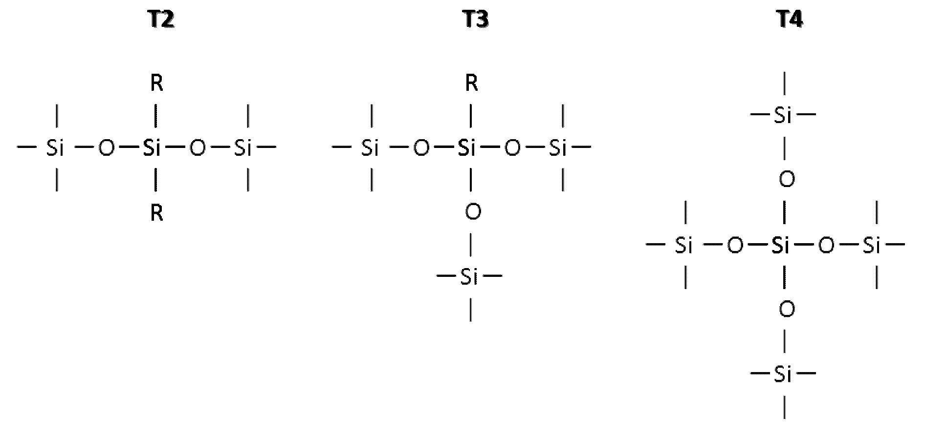
本開示の空隙層が前記シロキサン結合を有する場合、T2、T3及びT4の割合は、例えば、T2を「1」として相対的に表した場合、T2:T3:T4=1:[1~100]:[0~50]、1:[1~80]:[1~40]、1:[5~60]:[1~30]である。
本開示の空隙層において、前記ゲル状ケイ素化合物は、前述のとおり、シラン化合物が縮合又は部分的に縮合した化合物である。前記縮合は、例えば、脱水縮合などがあげられる。また、前記部分的に縮合した状態とは、例えば、前記シラン化合物に含まれる縮合性官能基(例えば、アルコキシ基等)のうち、一部の官能基が縮合しており、その他の官能基は縮合せずに縮合性官能基が残留している状態をいう。言い換えれば、例えば、前記シラン化合物のうち、一部のシラン化合物がシロキサン結合し、その他のシラン化合物が未結合の状態であるともいえる。前記未結合のシラン化合物の割合は、例えば、50%未満、30%以下、15%以下、である。
本開示の空隙層は、前記シラン化合物として、前述のとおり、1~3官能シラン化合物及び4官能シラン化合物を含む。前記シラン化合物として、例えば、1~3官能シラン化合物の中から少なくとも一つのシラン化合物を含み、さらに4官能シラン化合物を含むものであってもよい。前記1~3官能シラン化合物としては、例えば、1~3官能アルコキシシランがあげられる。前記4官能シラン化合物としては、例えば、4官能アルコキシシランがあげられる。前記1官能シラン化合物としては、例えば、トリメチルメトキシシラン(TMMS)、トリメチルエトキシシラン(TMES)、トリメチルプロポキシシラン(TMPS)等があげられる。前記2官能シラン化合物としては、例えば、ジメチルジメトキシシラン(DDMS)、ジメチルジエトキシシラン(DDES)、ジメチルジプロポキシシラン(DDPS)等があげられる。前記3官能シラン化合物としては、例えば、メチルトリメトキシシラン(MTMS)、メチルトリエトキシシラン(MTES)、メチルトリプロポキシシラン(MTPS)、3-アクリロキシプロピルトリエトキシシラン、ビニルトリメトキシシラン、ビニルトリエトキシシラン、4-ビニルブチルトリメトキシシラン、4-ビニルブチルトリエトキシシラン、8-ビニルオクチルトリメトキシシラン、8-ビニルオクチルトリエトキシシラン、10-メタクリロイルオキシデシルトリメトキシシラン、10-アクリロイルオキシデシルトリメトキシシラン、10-メタクリロイルオキシデシルトリエトキシシラン、10-アクリロイルオキシデシルトリエトキシシラン等があげられる。前記4官能シラン化合物としては、例えば、テトラメトキシシラン(TMOS)、テトラエトキシシラン(TEOS)、テトラプロポキシシラン(TPOS)等があげられる。
本開示の空隙層において、前記1~3官能シラン化合物の物質量に対する前記4官能シラン化合物の含有割合は、例えば、1~25mol%である。前記含有割合は、その下限が、例えば、2mol%以上、3mol%以上、又は3.5mol%以上であり、その上限が、例えば、20mol%以下、15mol%以下、又は10mol%以下であり、その範囲が、例えば、2~20mol%、3~15mol%、3.5~15mol%、又は3.5~10mol%である。なお、前記含有割合は、ゲル粉砕工程における粉砕の容易さの観点から高すぎないことが好ましい。また、前記含有割合は、低屈折率層の強度改善の観点から低すぎないことが好ましい。
本開示の空隙層は、例えば、添加剤の共存条件において前記ゲル状ケイ素化合物の粉砕物が化学的に結合した空隙層である。前記添加剤として、例えば、架橋反応促進剤及びその前駆体の少なくとも一方を含んでもよい。前記架橋反応促進剤は、例えば、酸性物質であってもよく、塩基性物質であってもよい。前記架橋反応促進剤は、例えば、前記ゲル状ケイ素化合物の粉砕物同士の化学的な結合(架橋結合)を促進する触媒ということもできる。また、前記架橋反応促進剤の前駆体は、例えば、光又は熱により前記架橋反応促進剤を発生する物質(架橋促進剤発生剤)ということもできる。
前記ゲル状ケイ素化合物同士を化学的に結合させる化学反応としては、シリカゾル分子に含まれる残留シラノール基の脱水縮合反応を利用することが好ましい。シラノール基の水酸基同士の反応を前記架橋反応促進剤で促進することで、短時間で空隙構造を硬化させる連続成膜が可能である。前記架橋反応促進剤としては、例えば、光活性触媒及び熱活性触媒があげられる。前記光活性触媒によれば、例えば、後述する結合工程において、加熱によらずに前記ゲル状ケイ素化合物同士を化学的に結合(例えば架橋結合)させることができる。これによれば、例えば、前記結合工程において、結合させる前記粉砕物の収縮が起こりにくいため、より高い空隙率を維持できる。例えば、前記光活性触媒に加え、又はこれに代えて、光により触媒を発生する物質(光触媒発生剤)を用いてもよいし、前記熱活性触媒に加え、又はこれに代えて、熱により触媒を発生する物質(熱触媒発生剤)を用いてもよい。前記光触媒発生剤としては、特に限定されないが、例えば、光塩基発生剤(光照射により塩基性触媒を発生する物質)、光酸発生剤(光照射により酸性触媒を発生する物質)等があげられ、光塩基発生剤が好ましい。前記光塩基発生剤としては、例えば、9-アントリルメチル N,N-ジエチルカルバメート(9-anthrylmethyl N,N-diethylcarbamate、商品名WPBG-018)、(E)-1-[3-(2-ヒドロキシフェニル)-2-プロペノイル]ピペリジン((E)-1-[3-(2-hydroxyphenyl)-2-propenoyl]piperidine、商品名WPBG-027)、1-(アントラキノン-2-イル)エチル イミダゾールカルボキシレート(1-(anthraquinon-2-yl)ethyl imidazolecarboxylate、商品名WPBG-140)、2-ニトロフェニルメチル 4-メタクリロイルオキシピペリジン-1-カルボキシラート(商品名WPBG-165)、1,2-ジイソプロピル-3-〔ビス(ジメチルアミノ)メチレン〕グアニジウム 2-(3-ベンゾイルフェニル)プロピオナート(商品名WPBG-266)、1,2-ジシクロヘキシル-4,4,5,5-テトラメチルビグアニジウム n-ブチルトリフェニルボラート(商品名WPBG-300)、及び2-(9-オキソキサンテン-2-イル)プロピオン酸1,5,7-トリアザビシクロ[4.4.0]デカ-5-エン(東京化成工業株式会社)、4-ピペリジンメタノールを含む化合物(商品名HDPD-PB100:ヘレウス社製)等があげられる。なお、前記「WPBG」を含む商品名は、いずれも和光純薬工業株式会社の商品名である。前記光酸発生剤としては、例えば、芳香族スルホニウム塩(商品名SP-170:ADEKA社)、トリアリールスルホニウム塩(商品名CPI101A:サンアプロ社)、芳香族ヨードニウム塩(商品名Irgacure250:チバ・ジャパン社)等があげられる。また、前記ゲル状ケイ素化合物の粉砕物同士を化学的に結合させる架橋反応促進剤は、前記光活性触媒及び前記光触媒発生剤に限定されず、例えば、熱活性触媒又は尿素のような熱触媒発生剤でもよい。前記ゲル状ケイ素化合物の粉砕物同士を化学的に結合させる架橋反応促進剤は、例えば、水酸化カリウム、水酸化ナトリウム、水酸化アンモニウム等の塩基触媒、塩酸、酢酸、シュウ酸等の酸触媒等があげられる。これらの中で、塩基触媒が好ましい。前記架橋反応促進剤及びその前駆体は、例えば、前記粉砕物(ゲル状ケイ素化合物)を含むゾル粒子液(例えば懸濁液)に、前記架橋反応促進剤及びその前駆体の少なくとも一方を塗工直前に添加して使用する、又は前記架橋反応促進剤及びその前駆体の少なくとも一方を溶媒に混合した混合液として使用することができる。前記混合液は、例えば、前記ゾル粒子液に直接添加して溶解した塗工液、前記架橋反応促進剤及びその前駆体の少なくとも一方を溶媒に溶解した溶液、又は、前記架橋反応促進剤及びその前駆体の少なくとも一方を溶媒に分散した分散液でもよい。前記溶媒は、特に制限されず、例えば、水、緩衝液等があげられる。前記架橋反応促進剤及びその前駆体の添加量は、特に限定されないが、例えば、前記ゲル状ケイ素化合物の重量に対し、例えば、0.01~20重量%、0.05~10重量%、又は0.1~5重量%である。
前記1~3官能シラン化合物及び前記4官能シラン化合物の合計の物質量に対して、前記架橋反応促進剤及びその前駆体の合計含有割合は、その下限が、例えば、1mol%以上、1.5mol%以上、2mol%以上、又は2.5mol%以上であり、その上限が、例えば、5mol%以下、4mol%以下、3.5mol%以下、又は3mol%以下である。
なお、本開示の空隙層において、前記シラン化合物として前記4官能シラン化合物を含まない場合、前記シラン化合物の合計の物質量に対して、前記架橋反応促進剤及びその前駆体の合計含有割合は、その下限が、例えば、1.5mol%以上、2mol%以上、又は2.5mol%以上であり、その上限が、例えば、5mol%以下、4mol%以下、3.5mol%以下、又は3mol%以下である。
また、前記添加剤として、例えば、架橋補助剤を含んでもよい。前記架橋補助剤は、例えば、ゲル状ケイ素化合物の粉砕物と前記架橋補助剤との化学的な結合により、前記ゲル状ケイ素化合物の粉砕物同士を間接的に結合させるための媒体ということもできる。前記架橋補助剤が、前記粉砕物同士の間に入り込み、前記粉砕物と前記架橋補助剤が各々相互作用もしくは結合することで、距離的に多少離れた前記粉砕物同士も結合させることが可能であり、効率よく強度を上げることが可能となる。
前記架橋補助剤としては、多架橋シランモノマーが好ましい。前記多架橋シランモノマーは、具体的には、例えば、2以上3以下のアルコキシシリル基を有し、アルコキシシリル基間の鎖長が炭素数1以上10以下であってもよく、炭素以外の元素も含んでもよい。前記架橋補助剤としては、例えば、ビス(トリメトキシシリル)エタン、ビス(トリエトキシシリル)エタン、ビス(トリメトキシシリル)メタン、ビス(トリエトキシシリル)メタン、ビス(トリエトキシシリル)プロパン、ビス(トリメトキシシリル)プロパン、ビス(トリエトキシシリル)ブタン、ビス(トリメトキシシリル)ブタン、ビス(トリエトキシシリル)ペンタン、ビス(トリメトキシシリル)ペンタン、ビス(トリエトキシシリル)ヘキサン、ビス(トリメトキシシリル)ヘキサン、ビス(トリメトキシシリル)-N-ブチル-N-プロピル-エタン-1,2-ジアミン、トリス-(3-トリメトキシシリルプロピル)イソシアヌレート、トリス-(3-トリエトキシシリルプロピル)イソシアヌレート等があげられる。前記架橋補助剤の添加量は、特に限定されないが、例えば、前記ゲル状ケイ素化合物の重量に対し、0.01~20重量%、0.05~15重量%、又は0.1~10重量%である。
前記1~3官能シラン化合物及び前記4官能シラン化合物の合計の物質量に対して、前記架橋補助剤の合計含有割合は、その下限が、例えば、1mol%以上、2mol%以上、2.5mol%以上、又は3mol%以上であり、その上限が、例えば、6mol%以下、5.5mol%以下、5mol%以下、4.5mol%以下、又は3.5mol%以下である。
なお、本開示の空隙層において、前記シラン化合物として前記4官能シラン化合物を含まない場合、前記シラン化合物の合計の物質量に対して、前記架橋補助剤の合計含有割合は、その下限が、例えば、2mol%以上、又は2.5mol%以上であり、その上限が、例えば、6mol%以下、5mol%以下、4mol%以下、3.5mol%以下、又は3mol%以下である。
本開示の空隙層は、例えば、孔構造を有している。前記空隙層における、孔の空隙サイズは、空隙(孔)の長軸の直径及び短軸の直径のうち、前記長軸の直径を指すものとする。空孔サイズは、例えば、5nm~200nmである。前記空隙サイズは、例えば、5nm以上、10nm以上、又は20nm以上であり、その上限が、例えば、200nm以下、150nm以下、100nm以下、50nm以下、40nm以下、又は30nm以下であり、その範囲が、例えば、5nm~200nm、又は10nm~100nmである。前記空隙サイズは、空隙構造を用いる用途に応じて好ましい空隙サイズが決まるため、例えば、目的に応じて、所望の空隙サイズに調整する必要がある。前記空隙サイズは、例えば、以下の方法により評価できる。
(空隙層の断面SEM観察)
本開示において、空隙層の形態は、SEM(走査型電子顕微鏡)を用いて観察及び解析できる。具体的には、例えば、前記空隙層を、冷却下でFIB加工(加速電圧:30kV)し、得られた断面サンプルについてFIB-SEM(FEI社製:商品名Helios NanoLab600、加速電圧:1kV)により、観察倍率100,000倍にて断面電子像を得ることができる。
本開示において、空隙層の形態は、SEM(走査型電子顕微鏡)を用いて観察及び解析できる。具体的には、例えば、前記空隙層を、冷却下でFIB加工(加速電圧:30kV)し、得られた断面サンプルについてFIB-SEM(FEI社製:商品名Helios NanoLab600、加速電圧:1kV)により、観察倍率100,000倍にて断面電子像を得ることができる。
(空隙サイズの評価)
本開示において、前記空隙サイズは、BET試験法により定量化できる。具体的には、細孔分布/比表面積測定装置(BELLSORP MINI/マイクロトラックベル社の商品名)のキャピラリに、サンプル(前記空隙層)を0.1g投入した後、室温で24時間、減圧乾燥を行って、空隙構造内の気体を脱気する。そして、前記サンプルに窒素ガスを吸着させることで、BETプロット及びBJHプロット、吸着等温線を描き、細孔分布を求める。これによって、空隙サイズが評価できる。
本開示において、前記空隙サイズは、BET試験法により定量化できる。具体的には、細孔分布/比表面積測定装置(BELLSORP MINI/マイクロトラックベル社の商品名)のキャピラリに、サンプル(前記空隙層)を0.1g投入した後、室温で24時間、減圧乾燥を行って、空隙構造内の気体を脱気する。そして、前記サンプルに窒素ガスを吸着させることで、BETプロット及びBJHプロット、吸着等温線を描き、細孔分布を求める。これによって、空隙サイズが評価できる。
本開示の空隙層は、例えば、前述のように孔構造(多孔質構造)を有していてもよく、例えば、前記孔構造が連続した連泡構造体であってもよい。前記連泡構造体とは、例えば、前記空隙層において、三次元的に、孔構造が連なっていることを意味し、前記孔構造の内部空隙が連続している状態ともいえる。多孔質体が連泡構造を有する場合、これにより、バルク中に占める空隙率を高めることが可能であるが、中空シリカのような独泡粒子を使用する場合は、連泡構造を形成できない。これに対して、前記空隙層は、ゾル粒子(ゾルを形成する多孔体ゲルの粉砕物)が三次元の樹状構造を有するために、塗工膜(前記多孔体ゲルの粉砕物を含むゾルの塗工膜)中で、前記樹状粒子が沈降・堆積することで、容易に連泡構造を形成することが可能である。また、前記空隙層は、より好ましくは、連泡構造が複数の細孔分布を有するモノリス構造を形成することが好ましい。前記モノリス構造は、例えば、ナノサイズの微細な空隙が存在する構造と、同ナノ空隙が集合した連泡構造として存在する階層構造を指すものとする。前記モノリス構造を形成する場合、例えば、微細な空隙で膜強度を付与しつつ、粗大な連泡空隙で高空隙率を付与し、膜強度と高空隙率とを両立することができる。それらのモノリス構造を形成するには、例えば、まず、前記粉砕物に粉砕する前段階の前記多孔体ゲルにおいて、生成する空隙構造の細孔分布を制御することが重要である。また、例えば、前記多孔体ゲルを粉砕する際、前記粉砕物の粒度分布を、所望のサイズに制御することで、前記モノリス構造を形成させることができる。
本開示の空隙層において、透明性を示すヘイズは、特に制限されず、その下限が、例えば、0.1%以上、0.2%以上、又は0.3%以上であり、その上限が、例えば、10%以下、5%以下、3%以下であり、その範囲が、例えば、0.1~10%、0.2~5%、又は0.3~3%である。
前記ヘイズは、例えば、以下のような方法により測定できる。
(ヘイズの評価)
空隙層(本開示の空隙層)を50mm×50mmのサイズにカットし、ヘイズメーター(村上色彩技術研究所社製:HM-150)にセットしてヘイズを測定する。ヘイズ値については、以下の式より算出を行う。
ヘイズ(%)=[拡散透過率(%)/全光線透過率(%)]×100(%)
空隙層(本開示の空隙層)を50mm×50mmのサイズにカットし、ヘイズメーター(村上色彩技術研究所社製:HM-150)にセットしてヘイズを測定する。ヘイズ値については、以下の式より算出を行う。
ヘイズ(%)=[拡散透過率(%)/全光線透過率(%)]×100(%)
屈折率は、一般に、真空中の光の波面の伝達速度と、媒質内の伝播速度との比を、その媒質の屈折率という。なお、本開示において、前記屈折率は、特に断らない限り、波長550nmにおいて測定した屈折率をいう。また、屈折率の測定方法は、特に限定されず、例えば、下記の方法により測定できる。
本開示の空隙層の屈折率は、前述のとおり、1.30以下である。前記空隙層の屈折率は、その上限が、例えば、1.30以下、1.30未満、1.26以下、1.25以下、1.25未満、1.24以下、1.23以下、又は1.22以下であり、その下限が、例えば、1.05以上、1.10以上、1.15以上、1.16以上、1.17以上、1.18以上、又は1.19以上であり、その範囲が、例えば、1.05以上1.30以下、1.05以上1.30未満、1.10以上1.25以下、1.15以上1.25未満、又は1.19以上1.25未満である。前記空隙層の屈折率の測定方法は、特に限定されず、例えば、下記の方法により測定できる。
前記空隙層の空隙率は、その下限が、例えば、30体積%以上、又は50体積%以上であり、その上限が、例えば、90体積%以下、75体積%以下、又は60体積%以下であり、その範囲が、例えば、30~90体積%、50~75体積%、又は50~60体積%である。
(空隙層の屈折率の評価)
アクリルフィルムに空隙層(本開示の空隙層)を形成した後に、50mm×50mmのサイズにカットし、これを粘着層でガラス板(厚み:3mm)の表面に貼合する。前記ガラス板の裏面中央部(直径20mm程度)を黒インクで塗りつぶして、前記ガラス板の裏面で反射しないサンプルを調製する。エリプソメーター(J.A.Woollam Japan社製:VASE)に前記サンプルをセットし、550nmの波長、入射角50~80度の条件で、屈折率を測定し、その平均値を屈折率とする。
アクリルフィルムに空隙層(本開示の空隙層)を形成した後に、50mm×50mmのサイズにカットし、これを粘着層でガラス板(厚み:3mm)の表面に貼合する。前記ガラス板の裏面中央部(直径20mm程度)を黒インクで塗りつぶして、前記ガラス板の裏面で反射しないサンプルを調製する。エリプソメーター(J.A.Woollam Japan社製:VASE)に前記サンプルをセットし、550nmの波長、入射角50~80度の条件で、屈折率を測定し、その平均値を屈折率とする。
温度85℃、湿度85%RHで500時間保持する加熱加湿耐久性試験後の、前記空隙層の空隙残存率は、例えば、その下限が、10体積%以上、20体積%以上、30体積%以上、40体積%以上、50体積%以上、60体積%以上、70体積%以上、80体積%以上、85体積%以上、又は85体積%を超える。前記空隙層の屈折率の測定方法は、特に限定されず、例えば、下記の方法により測定できる。
(空隙層の空隙残存率の評価)
作製した積層体を、温度85℃、湿度85%RHのオーブンに投入し、500時間の加熱加湿耐久性試験を行なう。前記加熱加湿耐久性試験後の空隙層の空隙箇所の埋まり度合をSEMで確認し、空隙率の残存率を算出することができる。
作製した積層体を、温度85℃、湿度85%RHのオーブンに投入し、500時間の加熱加湿耐久性試験を行なう。前記加熱加湿耐久性試験後の空隙層の空隙箇所の埋まり度合をSEMで確認し、空隙率の残存率を算出することができる。
本開示の空隙層の厚みは、特に制限されず、その下限が、例えば、0.05μm以上、又は0.1μm以上であり、その上限が、例えば、1000μm以下、100μm以下、10μm以下、5μm以下、又は2μm以下であり、その範囲が、例えば、0.05~1000μm、又は0.1~100μmである。
本開示の空隙層の形態は、特に制限されず、例えば、フィルム形状でもよいし、ブロック形状等でもよい。
本開示の空隙層の製造方法は、特に制限されないが、例えば、後述する空隙層の製造方法、又は国際公開第2019/065999号、国際公開第2019/065803号に記載された方法で製造することができる。当該公報の記載は、本明細書に参考として援用される。
本開示において、前記粘接着層は、特に限定されない。本開示において、前記粘接着層を形成する粘着剤又は接着剤は特に限定されず、例えば、一般的な粘着剤又は接着剤等が使用できる。前記粘着剤又は接着剤としては、例えば、アクリル系、ビニルアルコール系、シリコーン系、ポリエステル系、ポリウレタン系、ポリエーテル系等のポリマー製接着剤、ゴム系接着剤等があげられる。また、グルタルアルデヒド、メラミン、シュウ酸等のビニルアルコール系ポリマーの水溶性架橋剤等から構成される接着剤等もあげられる。これら粘着剤及び接着剤は、1種類のみ用いても、複数種類を併用(例えば、混合、積層等)してもよい。前記粘接着層の厚みは、特に制限されないが、例えば、0.1~100μm、5~50μm、10~30μm、又は12~25μmである。
本開示の積層体の前記粘接着層において、前記ナノインデンテーション硬さは、例えば、0.5MPa以上である。前記ナノインデンテーション硬さは、その下限が、例えば、0.55MPa以上、0.6MPa以上、又は0.65MPa以上であってもよく、その上限が、例えば、2.0MPa以下、1.5MPa以下、1.3MPa以下、又は1.1MPa以下であってもよい。前記ナノインデンテーション硬さの測定方法は、特に限定されず、例えば、下記の方法により測定できる。
(ナノインデンテーション硬さの評価)
測定用サンプルを1cm角程度に切り出して所定の支持体に固定し、本開示の積層体における粘接着層のナノインデーション硬さを下記条件にて測定する。ナノインデンテーション硬さは、ナノインデンテーション法により測定することができる。
・分析装置:Hysitron Inc.製、Triboindenter
・使用圧子:Conical(球形:直径20μm)
・測定方法:単一押し込み測定
・測定温度:室温
・押し込み深さ:2000nm
測定用サンプルを1cm角程度に切り出して所定の支持体に固定し、本開示の積層体における粘接着層のナノインデーション硬さを下記条件にて測定する。ナノインデンテーション硬さは、ナノインデンテーション法により測定することができる。
・分析装置:Hysitron Inc.製、Triboindenter
・使用圧子:Conical(球形:直径20μm)
・測定方法:単一押し込み測定
・測定温度:室温
・押し込み深さ:2000nm
測定によって得られる最大荷重(Pmax)と接触投影面積(A)から、下記式によってナノインデンテーション硬さを算出する。
ナノインデンテーション硬さ=Pmax/A
ナノインデンテーション硬さ=Pmax/A
なお、前記ナノインデンテーション硬さは、粘着層表面及び粘着層断面のいずれのナノインデンテーション硬さであってもよい。
本開示の積層体において、引張試験機を用いて引張速度0.3m/minで測定される前記空隙層と前記粘接着層との層間のピール強度は、例えば、3N/25mm以上である。前記ピール強度は、その下限が、例えば、3.5N/25mm以上、4.0N/25mm以上、又は5.0N/25mm以上であってもよい。本開示の積層体の層間の機械的強度は、前記ピール強度が高いほど向上するため、前記ピール強度の上限値は特に限定されないが、例えば、20N/25mm以下、15N/25mm以下、又は10N/25mm以下である。前記ピール強度は、例えば、前記空隙層の凝集破壊に起因して測定されるピール強度である。前記ピール強度の測定方法は、特に限定されず、例えば、下記の方法により測定できる。
(層間のピール強度の評価)
樹脂フィルム基材上に空隙層(本開示の空隙層)と粘接着層(本開示の積層体における粘接着層)が形成されたものを用意し、前記樹脂フィルム基材において前記空隙層と反対側にアクリル粘着層(厚み20μm)を貼合する。貼り合わせたサンプルを、50mm×25mmにカットして粘着テープ片を作製する。つぎに、空隙層側の粘接着層(厚み10μm)を、25mm×100mmの短冊状にカットしたPETフィルム(T100:三菱樹脂フィルム社製)に貼合し、前記樹脂フィルム基材側のアクリル粘着層をガラスとラミネートして固定する。このように作製したサンプルを、チャック間距離が100mmになるように引張試験機(株式会社島津製作所製、商品名:オートグラフ(登録商標)AG-Xplus)にチャッキングした後、0.3m/minの引張速度で180°ピール試験を行う。50mmピール試験をN=3回実施し、その平均試験力を、前記層間のピール強度とする。
樹脂フィルム基材上に空隙層(本開示の空隙層)と粘接着層(本開示の積層体における粘接着層)が形成されたものを用意し、前記樹脂フィルム基材において前記空隙層と反対側にアクリル粘着層(厚み20μm)を貼合する。貼り合わせたサンプルを、50mm×25mmにカットして粘着テープ片を作製する。つぎに、空隙層側の粘接着層(厚み10μm)を、25mm×100mmの短冊状にカットしたPETフィルム(T100:三菱樹脂フィルム社製)に貼合し、前記樹脂フィルム基材側のアクリル粘着層をガラスとラミネートして固定する。このように作製したサンプルを、チャック間距離が100mmになるように引張試験機(株式会社島津製作所製、商品名:オートグラフ(登録商標)AG-Xplus)にチャッキングした後、0.3m/minの引張速度で180°ピール試験を行う。50mmピール試験をN=3回実施し、その平均試験力を、前記層間のピール強度とする。
前記積層体の状態で測定される本開示の空隙層の屈折率は、例えば、1.30以下である。前記積層体の状態で測定される空隙層の屈折率は、その上限が、例えば、1.30以下、1.30未満、1.26以下、1.25以下、1.25未満、1.24以下、1.23以下、又は1.22以下であり、その下限が、例えば、1.05以上、1.10以上、1.15以上、1.16以上、1.17以上、1.18以上、又は1.19以上であり、その範囲が、例えば、1.05以上1.30以下、1.05以上1.30未満、1.10以上1.25以下、1.15以上1.25未満、又は1.19以上1.25未満である。前記積層体の状態で測定される本開示の空隙層の屈折率の測定方法は、特に限定されず、例えば、下記の方法により測定できる。
(積層体の状態で測定される空隙層の屈折率の評価)
空隙層上に粘接着層を設けた積層体(ガラス/粘接着層/空隙層/アクリル基材)の基材面側に、プリズムカプラ(メトリコン社製)のプリズムを密着させ、レーザーを用いて全反射臨界角を測定する。測定した臨界角の値から屈折率を算出することができる。
空隙層上に粘接着層を設けた積層体(ガラス/粘接着層/空隙層/アクリル基材)の基材面側に、プリズムカプラ(メトリコン社製)のプリズムを密着させ、レーザーを用いて全反射臨界角を測定する。測定した臨界角の値から屈折率を算出することができる。
本開示の積層体は、例えば、前記屈折率をX、前記ピール強度をYとしたときに、下記条件(1)を満たすものであってもよい。図4に、条件(1)におけるピール強度と屈折率の関係を示すグラフを示す。なお、図4において、横軸は屈折率であり、縦軸はピール強度(N/25mm)を示す。
条件(1):Y≧80X-93.8
条件(1):Y≧80X-93.8
また、本開示の積層体は、例えば、前記屈折率をX、前記ピール強度をYとしたときに、下記条件(2)を満たすものであってもよい。図4に、条件(1)におけるピール強度と屈折率の関係を示すグラフを示す。
条件(2):Y≧100X-117
条件(2):Y≧100X-117
前記条件(1)又は前記条件(2)を満たす場合、例えば、低屈折率でありながらピール強度が高い(すなわち、機械的強度に優れる)積層体を得ることができる。前記条件(1)及び前記条件(2)を満たすために、特に限定されないが、例えば、前記4官能シラン化合物や前記添加剤の種類、含有割合等を適宜調整してもよい。
本開示において、前記中間層は、特に限定されないが、例えば、前述のとおり、前記空隙層の一部が前記粘接着層の一部と合一することにより形成された層である。前記中間層の厚みは、特に制限されないが、例えば、1~1500nm、5~1000nm、10~800nm、又は20~500nmである。
本開示の積層体の形態は、特に制限されないが、フィルム形状が通常である。
本開示の積層体は、例えば、ロール体である。また、本開示の積層体は、例えば、前述のように、さらに樹脂フィルムを含み、長尺な前記樹脂フィルム上に、前記空隙層が形成されてもよい。この場合、本開示の積層体には別の長尺フィルムが積層されていてもよく、前記樹脂フィルムと前記空隙層とを含む本開示の積層体に、別の長尺樹脂フィルム(例えば、合紙、離型フィルム、表面保護フィルム等)を積層した後、ロール体に巻かれた形態であってもよい。
本開示の積層体の製造方法は、特に制限されないが、例えば、以下に示す本開示の製造方法により製造することができる。また、樹脂フィルムを含まない本開示の光学積層体の製造方法については、特に断らない限り、樹脂フィルムを用いない以外は本開示の積層体の製造方法と同様にして行うことができる。
[2.空隙層の製造方法、積層体の製造方法]
本開示の空隙層、及び本開示の積層体を製造する方法は、特に限定されないが、例えば、以下に説明する製造方法により行うことができる。ただし、以下の説明は例示であり、本開示をなんら限定しない。
本開示の空隙層、及び本開示の積層体を製造する方法は、特に限定されないが、例えば、以下に説明する製造方法により行うことができる。ただし、以下の説明は例示であり、本開示をなんら限定しない。
本開示の空隙層を含む積層体の製造方法は、例えば、前記空隙層を形成する空隙層形成工程、及び、前記空隙層上に前記粘接着層を形成する粘接着層形成工程を含む。前記積層体の製造方法は、さらに、前記空隙層を、前記粘接着層と反応させて前記中間層を形成する中間層形成工程を含んでもよい。
前記空隙層形成工程(本開示の空隙層の製造方法)は、前述のとおり、ゲル状シリカ合成工程、ゲル粉砕工程、及び結合工程を含む。前記空隙層形成工程(本開示の空隙層の製造方法)は、前記ゲル状シリカ合成工程、前記ゲル粉砕工程、及び前記結合工程以外の他の工程を含んでいてもよいし、含んでいなくてもよい。前記他の工程としては、特に限定されないが、例えば、後述する塗工工程、乾燥工程等があげられる。
前記ゲル状シリカ合成工程は、前記シラン化合物を縮合又は部分的に縮合させてゲル状ケイ素化合物を合成する工程を含む。前記ゲル状シリカ合成工程は、例えば、塊状の多孔体を溶媒中でゲル化してゲルとする工程を含んでもよい。この場合、例えば、後述する複数段階の粉砕段階のうち最初の粉砕段階(例えば、後述する第1の粉砕段階)において、前記ゲル状シリカ合成工程によりゲル化した前記ゲルを使用する。
前記空隙層の製造方法は、例えば、ゲル化した前記ゲルを溶媒中で熟成する熟成工程を含む。この場合、例えば、前記複数段階の粉砕段階のうち最初の粉砕段階(例えば、前記第1の粉砕段階)において、前記熟成工程後の前記ゲルを使用する。
前記ゲル粉砕工程は、前記ゲル状ケイ素化合物を粉砕して粉砕物を得る工程を含む。前記ゲル粉砕工程は、1段階でもよいが、複数の粉砕段階に分けて行うことが好ましい。前記粉砕段階数は、特に限定されず、例えば、2段階でもよいし、3段階以上でもよい。
前記第1の粉砕段階後の前記ゲルの体積平均粒子径は、例えば、0.5~100μm、1~100μm、1~50μm、2~20μm、又は3~10μmであってもよい。前記第2の粉砕段階後の前記ゲルの体積平均粒子径は、例えば、10~1000nm、100~500nm、又は200~300nmであってもよい。前記体積平均粒子径は、前記ゲルを含む液(ゲル含有液)における前記粉砕物の粒度バラツキを示す。前記体積平均粒子径は、例えば、動的光散乱法、レーザー回折法等の粒度分布評価装置、及び走査型電子顕微鏡(SEM)、透過型電子顕微鏡(TEM)等の電子顕微鏡等により測定することができる。
本開示の空隙層の製造方法は、例えば、前記ゲル状シリカ合成工程の後、前記溶媒を他の溶媒に置換する前記溶媒置換工程を行う。この場合、例えば、前記複数段階の粉砕段階のうち最初の粉砕段階(例えば、前記第1の粉砕段階)において、前記他の溶媒中の前記ゲルを使用する。
本開示の空隙層の製造方法の前記複数段階の粉砕段階の少なくとも一つ(例えば、前記第1の粉砕段階及び前記第2の粉砕段階の少なくとも一方)において、例えば、前記液のせん断粘度を測定しながら前記多孔体の粉砕を制御する。
本開示の空隙層の製造方法の前記複数段階の粉砕段階の少なくとも一つ(例えば、前記第1の粉砕段階及び前記第2の粉砕段階の少なくとも一方)を、例えば、高圧メディアレス粉砕により行う。
なお、以下、本開示の空隙層の製造方法において、前記ゲル粉砕工程を含む工程により得られるゲル粉砕物含有液を、単に「ゲル粉砕物含有液」ということがある。
前記ゲル粉砕物含有液によれば、例えば、その塗工膜を形成し、結合工程により前記塗工膜中の前記粉砕物を化学的に結合させることで、機能性多孔体としての前記空隙層を形成できる。前記ゲル粉砕物含有液によれば、例えば、前記空隙層を、様々な対象物に付与することができる。したがって、前記ゲル粉砕物含有液及びその製造方法は、例えば、前記空隙層の製造において有用である。
前記ゲル粉砕物含有液は、例えば、極めて優れた均一性を有しているため、例えば、前記空隙層を、光学部材等の用途に適用した場合、その外観を良好にすることができる。
前記ゲル粉砕物含有液は、例えば、前記ゲル粉砕物含有液を基板上に塗工(コーティング)し(塗工工程)、さらに乾燥することで(乾燥工程)、高い空隙率を有する層(空隙層)を得るための、ゲル粉砕物含有液であってもよい。
前記塗工工程において、前記ゲル粉砕物含有液の塗工方法は特に限定されず、一般的な塗工方法を採用できる。前記塗工方法としては、例えば、スロットダイ法、リバースグラビアコート法、マイクログラビア法(マイクログラビアコート法)、ディップ法(ディップコート法)、スピンコート法、刷毛塗り法、ロールコート法、フレキソ印刷法、ワイヤーバーコート法、スプレーコート法、エクストルージョンコート法、カーテンコート法、リバースコート法等が挙げられる。これらの中で、生産性、塗膜の平滑性等の観点から、エクストルージョンコート法、カーテンコート法、ロールコート法、マイクログラビアコート法等が好ましい。前記ゲル粉砕物含有液の塗工量は、特に限定されず、例えば、前記空隙層の厚みが適切になるように、適宜設定可能である。前記空隙層の厚みは、特に限定されず、例えば、前述の通りである。
前記乾燥工程において、前記ゲル粉砕物含有液を乾燥し(すなわち、前記ゲル粉砕物含有液に含まれる分散媒を除去し)、前記乾燥後の塗工膜(空隙層の前駆体)を形成する。前記乾燥工程における乾燥処理の温度は、例えば、50~250℃、60~150℃、70~130℃であり、前記乾燥処理の時間は、例えば、0.1~30分、0.2~10分、0.3~3分である。乾燥処理温度、及び時間については、例えば、連続生産性や高い空孔率の発現の関連では、より低く短いほうが好ましい。条件が厳しすぎると、例えば、基材が樹脂フィルムの場合、前記基材のガラス転移温度に近づくことで、前記基材が乾燥炉の中で伸展してしまい、塗工直後に、形成された空隙構造にクラック等の欠点が発生する可能性がある。一方で、条件が緩すぎる場合、例えば、ロールトゥロール加工において乾燥炉を出たタイミングで残留溶媒を含むため、次工程でロールと擦れた際に、スクラッチ傷が入る等の外観上の不具合が発生する可能性がある。
前記乾燥処理の方法は、例えば、自然乾燥でもよいし、加熱乾燥でもよいし、減圧乾燥でもよい。前記乾燥方法は、特に制限されず、例えば、一般的な加熱手段が使用できる。前記加熱手段は、例えば、熱風器、加熱ロール、遠赤外線ヒーター等が挙げられる。中でも、工業的に連続生産することを前提とした場合は、加熱乾燥を用いることが好ましい。
前記結合工程は、前記粉砕物を化学的に結合させる工程を含む。前記結合工程は、例えば、事前に前記ゲル粉砕物含有液に添加された触媒もしくは触媒発生剤を含む前記塗工膜に対し光照射もしくは加熱、又は、前記塗工膜に、前記触媒を吹き付けてから光照射もしくは加熱、又は、前記触媒もしくは前記触媒発生剤を吹き付けながら光照射もしくは加熱することによって、行うことができる。前記触媒は、例えば、前記架橋反応促進剤でも良く、前記空隙層の強度を向上させる強度向上剤であっても良く、前記架橋促進剤が前記強度向上剤を兼ねていてもよい。
前記光照射における、光照射の積算光量は、特に限定されないが、@360nm換算で、例えば、200~800mJ/cm2、250~600mJ/cm2、又は300~400mJ/cm2である。照射量が十分でなく触媒発生剤の光吸収による分解が進まず効果が不十分となることを防止する観点からは、200mJ/cm2以上の積算光量がよい。また、空隙層下の基材にダメージがかかり、熱ジワが発生することを防止する観点からは、800mJ/cm2以下の積算光量がよい。
前記加熱における、加熱温度及び加熱時間は特に限定されず、前記加熱処理の条件は、特に制限されず、前記加熱温度は、例えば、50~250℃、60~150℃、70~130℃であり、前記加熱時間は、例えば、0.1~30分、0.2~10分、0.3~3分である。又は、前述のとおり塗工された前記ゲル粉砕物含有液を乾燥する工程が、前記触媒存在下での化学反応を行う工程を兼ねていてもよい。すなわち、塗工された前記ゲル粉砕物含有液(例えば懸濁液)を乾燥する工程において、前記触媒存在下での化学反応により、前記粉砕物同士を化学的に結合させてもよい。この場合において、前記乾燥工程後に前記塗工膜をさらに加熱することにより、前記粉砕物(微細孔粒子)同士をさらに強固に結合させてもよい。さらに、前記触媒存在下での化学反応は、前記微細孔粒子含有液(例えば懸濁液)を作製する工程、及び、前記微細孔粒子含有液を塗工する工程においても起こる場合があると推測される。しかしながら、この推測は、本開示を何ら限定しない。
前記粘接着層形成工程は、例えば、前記粘接着剤塗工液を基材に塗布する粘接着剤塗工液塗布工程と、前記粘接着剤塗工液が塗布された前記基材を加熱乾燥する加熱乾燥工程と、を含んでいてもよい。例えば、基材上に前記粘接着層が積層された粘着テープ等の、前記粘接着層側を、前記空隙層の上に貼り合せることにより、前記空隙層上に前記粘接着層を形成してもよい。この場合、前記粘着テープ等の基材は、そのまま貼り合せたままにしてもよいし、前記粘接着層から剥離してもよい。特に、基材を剥離して、基材を有しない(基材レスの)積層体とすることで、厚みを大幅に低減することができ、デバイス等の厚み増加を抑制できる。本開示において、前記粘接着層は、例えば、前述のとおり、前記粘接着剤塗工液を用いて製造することができる。
前記粘接着層形成工程は、例えば、以下のようにして行うことができる。まず、前記粘接着剤塗工液の全成分を混合する混合工程により、前記粘接着剤塗工液を製造する。前記粘接着剤塗工液は、例えば、(メタ)アクリル系ポリマーを含んでいてもよく、また、例えば、さらに架橋剤(例えばイソシアネート系架橋剤やエポキシ系架橋剤)を含んでいてもよいし、含んでいなくてもよい。前記粘接着剤塗工液は、例えば、前記(メタ)アクリル系ポリマーと、反応性二重結合を1分子中に1つ又は2つ有するモノマーと架橋剤と、有機過酸化物とを含んでいてもよい。このとき、前記粘接着剤塗工液が、他の成分を含む場合は、前記他の成分も一緒に混合してもよい。例えば、前記(メタ)アクリル系ポリマー製造時の重合溶媒を除去せずに、そのまま前記粘接着剤塗工液の成分として混合してもよい。また、前記粘接着剤塗工液の製造方法は、前記混合工程以外の他の工程を含んでいてもよいが、含んでいなくてもよく、単に前記混合工程により前記粘接着剤塗工液の全成分を混合するのみでもよい。
つぎに、前記粘接着剤塗工液を基材に塗布する(粘接着剤塗工液塗布工程)。前記基材は、特に制限されず、例えば、フィルム等の基材であってもよい。前記基材は、例えば、熱可塑性樹脂製の基材、ガラス製の基材、シリコンに代表される無機基板、熱硬化性樹脂等で成形されたプラスチック、半導体等の素子、カーボンナノチューブに代表される炭素繊維系材料等が好ましく使用できるが、これらに限定されない。前記基材の形態は、例えば、フィルム、プレート等があげられる。前記熱可塑性樹脂は、例えば、ポリエチレンテレフタレート(PET)、アクリル、セルロースアセテートプロピオネート(CAP)、シクロオレフィンポリマー(COP)、トリアセチルセルロース(TAC)、ポリエチレンナフタレート(PEN)、ポリエチレン(PE)、ポリプロピレン(PP)等があげられる。また、前記粘接着剤塗工液塗布工程において、前記粘接着剤塗工液の塗布厚みは、特に限定されないが、例えば、乾燥後の粘接着層の厚みが所定の厚みになるように適宜調整すればよい。乾燥後の粘接着層の厚みも特に限定されないが、例えば、後述のとおりである。
つぎに、前記粘接着剤塗工液が塗布された前記基材を加熱乾燥する(加熱乾燥工程)。この加熱乾燥工程において、加熱乾燥の温度は、特に限定されないが、例えば、50℃以上、80℃以上、100℃以上、又は155℃以上であってもよく、例えば、200℃以下、180℃以下、又は160℃以下であってもよい。加熱乾燥の時間は、特に限定されないが、例えば、0.5分以上、1分以上、又は3分以上であってもよく、例えば、60分以下、30分以下、20分以下、又は10分以下であってもよい。この加熱乾燥工程において、例えば、前記(メタ)アクリル系ポリマーと架橋剤との間で、架橋反応及びグラフト重合が起こる。これにより、例えば、前述のとおり、前記粘接着剤塗工液中に存在する半高分子ポリマーの量が減少し、前記粘接着層が前記第1の光学シートの前記凹部中に侵入しにくくなる。以上のようにして、本開示の積層体に用いる前記粘接着層を製造できる。
つぎに、前述のとおり、前記粘接着層と前記空隙層とを貼り合せる(貼合工程)。この方法は特に限定されないが、例えば、前述のとおり、基材上に前記本開示の粘接着層が積層された粘着テープ等の、前記粘接着層側を、前記空隙層の上に貼り合せることにより、前記空隙層上に前記粘接着層を形成してもよい。以上のようにして、前記本開示の積層体を製造できる。
前記粘接着層の厚みは、特に制限されないが、例えば、0.1~100μm、5~50μm、10~30μm、又は12~25μmである。
前記本開示の積層体の製造方法において、例えば、さらに、前記貼合工程後に前記粘接着層及び前記空隙層を加熱する加熱工程を行ってもよい。以下において、この加熱工程を「エージング工程」という場合がある。前記加熱工程(エージング工程)において、加熱温度は、特に限定されないが、例えば、40℃以上、45℃以上、又は50℃以上であってもよく、例えば、80℃以下、70℃以下、60℃以下、又は55℃以下であってもよい。加熱時間は、特に限定されないが、例えば、1分以上、10分以上、60分以上、又は1800分以上であってもよく、例えば、3000分以下、2800分以下、2500分以下、又は2000分以下であってもよい。このエージング工程において、例えば、前記空隙層と前記粘接着層との合一によって前記中間層が形成される。そして、例えば、前記中間層がストッパーとなり、前記空隙層の空隙が粘着剤によって埋まることによる空隙率の減少を抑制できる。なお、前記空隙層と前記粘接着層との合一は、前記粘接着層が前記空隙層の空隙に埋まり込んで且つ化学的に結合したものであってもよいし、前記粘接着層が前記空隙層の空隙に埋まり込んだものであってもよい。
前記粘接着層により、前記空隙層を、物理的ダメージ(特に擦傷)から保護することが可能である。また、前記粘接着層は、基材を有しない(基材レスの)空隙層含有粘接着シートとしても前記空隙層が潰れないように、耐圧性に優れたものが好ましいが、特に限定されない。
このようにして得られる本開示の積層体は、例えば、前述のとおり、さらに、他のフィルム(層)と積層して、前記空隙層(多孔質構造)を含む積層構造体としてもよい。この場合、前記積層構造体において、各構成要素は、例えば、前記粘接着層(粘着剤又は接着剤)を介して積層させてもよい。
前記各構成要素の積層は、例えば、効率的であることから、長尺フィルムを用いた連続処理(いわゆるRoll to Roll等)により積層を行ってもよく、基材が成形物・素子等の場合はバッチ処理を行ったものを積層してもよい。
[3.光学部材]
本開示の光学部材は、前述のように、本開示の空隙層、又は本開示の積層体を含む。本開示の光学部材は、本開示の空隙層、又は本開示の積層体を含むことが特徴であって、その他の構成は何ら制限されない。本開示の光学部材は、例えば、前記空隙層、又は前記積層体の他に、他の層をさらに含んでもよい。本開示の光学部材は、例えば、ロール状である。
本開示の光学部材は、前述のように、本開示の空隙層、又は本開示の積層体を含む。本開示の光学部材は、本開示の空隙層、又は本開示の積層体を含むことが特徴であって、その他の構成は何ら制限されない。本開示の光学部材は、例えば、前記空隙層、又は前記積層体の他に、他の層をさらに含んでもよい。本開示の光学部材は、例えば、ロール状である。
[4.光学装置]
本開示の光学装置は、前述のように、本開示の光学部材を含む。本開示の光学装置は、特に限定されないが、例えば、画像表示装置でも照明装置でもよい。前記画像表示装置としては、例えば、液晶ディスプレイ、有機EL(Electro Luminescence)ディスプレイ、マイクロLED(Light Emitting Diode)ディスプレイ等があげられる。前記照明装置としては、例えば、有機EL照明等があげられる。
本開示の光学装置は、前述のように、本開示の光学部材を含む。本開示の光学装置は、特に限定されないが、例えば、画像表示装置でも照明装置でもよい。前記画像表示装置としては、例えば、液晶ディスプレイ、有機EL(Electro Luminescence)ディスプレイ、マイクロLED(Light Emitting Diode)ディスプレイ等があげられる。前記照明装置としては、例えば、有機EL照明等があげられる。
つぎに、本開示の実施例について説明する。ただし、本開示は、以下の実施例に限定されない。
なお、以下の参考例、実施例及び比較例において、各物質の部数(相対的な使用量)は、特に断らない限り、質量部(重量部)である。以下の参考例、実施例及び比較例において、粘接着剤としては、後述する粘着剤(粘着剤組成物)を用いた。以下の参考例、実施例及び比較例において、「粘着剤層」は、「粘接着層」に該当する。すなわち、以下の参考例、実施例及び比較例においては、特に断らない限り、「粘着剤層」と「粘接着層」とは同義である。
また、以下の参考例、実施例及び比較例において、ナノインデンテーション硬さ、積層体の状態で測定される空隙層の屈折率(屈折率(積層体))、及び空隙層のみを測定した場合における屈折率(屈折率(空隙層))、ピール強度、及び空隙残存率は、それぞれ、実施形態に記載した方法により測定した。
なお、以下の各参考例、実施例及び比較例における粘接着層においては、塗工した粘着剤の加熱乾燥によって、ポリマー(アクリル系ポリマー)が架橋剤により架橋され、架橋構造が形成されたと推測されるが、架橋構造については確認していない。
[参考例1:粘接着層(粘着剤1)の形成]
下記(1)~(3)の手順により、本参考例(参考例1)の粘接着層を形成した。
下記(1)~(3)の手順により、本参考例(参考例1)の粘接着層を形成した。
(1)アクリル系ポリマー溶液の調製
撹拌羽根、温度計、窒素ガス導入管、冷却器を備えた4つ口フラスコ内に、ブチルアクリレート90.7部、N-アクリロイルモルホリン6部、アクリル酸3部、2-ヒドロキシブチルアクリレート0.3部、及び、重合開始剤として2,2’-アゾビスイソブチロニトリル0.1重量部を、酢酸エチル100gと共に入れた。つぎに、前記4つ口フラスコ内の内容物を緩やかに撹拌しながら窒素ガスを導入して窒素置換した。その後、前記4つ口フラスコ内の液温を55℃付近に保って8時間重合反応を行い、アクリル系ポリマー溶液を調製した。
撹拌羽根、温度計、窒素ガス導入管、冷却器を備えた4つ口フラスコ内に、ブチルアクリレート90.7部、N-アクリロイルモルホリン6部、アクリル酸3部、2-ヒドロキシブチルアクリレート0.3部、及び、重合開始剤として2,2’-アゾビスイソブチロニトリル0.1重量部を、酢酸エチル100gと共に入れた。つぎに、前記4つ口フラスコ内の内容物を緩やかに撹拌しながら窒素ガスを導入して窒素置換した。その後、前記4つ口フラスコ内の液温を55℃付近に保って8時間重合反応を行い、アクリル系ポリマー溶液を調製した。
(2)アクリル系粘着剤組成物の調製
前記(1)で得られたアクリル系ポリマー溶液の固形分100部に対して、イソシアネート系架橋剤(日本ポリウレタン工業社製の商品名「コロネートL」、トリメチロールプロパンのトリレンジイソシアネートのアダクト体)0.2部、ベンゾイルパーオキサイド(日本油脂社製の商品名「ナイパーBMT」)0.3部、γ-グリシドキシプロピルメトキシシラン(信越化学工業社製の商品名「KBM-403」)0.1部を配合したアクリル系粘着剤組成物(アクリル系粘着剤溶液)を調製した。
前記(1)で得られたアクリル系ポリマー溶液の固形分100部に対して、イソシアネート系架橋剤(日本ポリウレタン工業社製の商品名「コロネートL」、トリメチロールプロパンのトリレンジイソシアネートのアダクト体)0.2部、ベンゾイルパーオキサイド(日本油脂社製の商品名「ナイパーBMT」)0.3部、γ-グリシドキシプロピルメトキシシラン(信越化学工業社製の商品名「KBM-403」)0.1部を配合したアクリル系粘着剤組成物(アクリル系粘着剤溶液)を調製した。
(3)粘接着層の形成
前記(2)で得られたアクリル系粘着剤組成物を、シリコーン処理を施したポリエチレンテレフタレート(PET)フィルム(三菱化学ポリエステルフィルム社製、厚さ:38μm)の片面に、乾燥後の粘着剤層の厚さが10μmになるように塗布し、150℃で3分間乾燥を行い、粘着剤層(粘接着層)である粘着剤1を形成した。
前記(2)で得られたアクリル系粘着剤組成物を、シリコーン処理を施したポリエチレンテレフタレート(PET)フィルム(三菱化学ポリエステルフィルム社製、厚さ:38μm)の片面に、乾燥後の粘着剤層の厚さが10μmになるように塗布し、150℃で3分間乾燥を行い、粘着剤層(粘接着層)である粘着剤1を形成した。
[参考例2:粘接着層(粘着剤2)の形成]
下記(1)~(3)の手順により、本参考例(参考例2)の粘接着層を形成した。
下記(1)~(3)の手順により、本参考例(参考例2)の粘接着層を形成した。
(1)(メタ)アクリル系ポリマー(A1)溶液の調製
攪拌羽根、温度計、窒素ガス導入管、冷却器を備えた4つ口フラスコに、ブチルアクリレート79.5部、N-アクリロイルモルホリン15部、アクリル酸5部、4-ヒドロキシブチルアクリレート0.5部を含有するモノマー混合物を仕込んだ。さらに、前記モノマー混合物100部に対して、重合開始剤として2,2'-アゾビスイソブチロニトリル0.1部を酢酸エチル70部と共に仕込み、緩やかに撹枠しながら窒素ガスを導入して窒素置換した後、フラスコ内の液温を55℃付近に保って2時間重合反応を行って、重量平均分子量(Mw)300万、Mw/Mn=2.5の(メタ)アクリル系ポリマー(A1) の溶液を調製した。
攪拌羽根、温度計、窒素ガス導入管、冷却器を備えた4つ口フラスコに、ブチルアクリレート79.5部、N-アクリロイルモルホリン15部、アクリル酸5部、4-ヒドロキシブチルアクリレート0.5部を含有するモノマー混合物を仕込んだ。さらに、前記モノマー混合物100部に対して、重合開始剤として2,2'-アゾビスイソブチロニトリル0.1部を酢酸エチル70部と共に仕込み、緩やかに撹枠しながら窒素ガスを導入して窒素置換した後、フラスコ内の液温を55℃付近に保って2時間重合反応を行って、重量平均分子量(Mw)300万、Mw/Mn=2.5の(メタ)アクリル系ポリマー(A1) の溶液を調製した。
(2)(メタ)アクリル系粘着剤組成物の調製
得られた前記(メタ)アクリル系ポリマー(A1)の溶液の固形分100部に対して、イソシアネート架橋剤(日本ポリウレタン工業社製の商品名「コロネートL」、トリメチロールプロパンのトリレンジイソシアネートのアダクト体)0.2部、エポキシ架橋剤1,3-ビス(N,N-ジグリシジルアミノメチル)シクロヘキサン(三菱ガス化学社製の商品名「テトラッドC」)0.2部を配合して、アクリル系粘着剤組成物の溶液を調製した。
得られた前記(メタ)アクリル系ポリマー(A1)の溶液の固形分100部に対して、イソシアネート架橋剤(日本ポリウレタン工業社製の商品名「コロネートL」、トリメチロールプロパンのトリレンジイソシアネートのアダクト体)0.2部、エポキシ架橋剤1,3-ビス(N,N-ジグリシジルアミノメチル)シクロヘキサン(三菱ガス化学社製の商品名「テトラッドC」)0.2部を配合して、アクリル系粘着剤組成物の溶液を調製した。
(3)粘接着層の形成
次いで、前記アクリル系粘着剤組成物の溶液を、シリコーン系剥離剤で処理されたポリエチレンテレフタレートフィルム(セパレータフィルム:三菱化学ポリエステルフィルム(株)製、MRF38)の片面に、乾燥後の粘着剤層の厚さが10μmになるように塗布し、155℃で1分間乾燥を行い、セパレータフィルムの表面に粘着剤層(粘接着層)である粘着剤2を形成した。
次いで、前記アクリル系粘着剤組成物の溶液を、シリコーン系剥離剤で処理されたポリエチレンテレフタレートフィルム(セパレータフィルム:三菱化学ポリエステルフィルム(株)製、MRF38)の片面に、乾燥後の粘着剤層の厚さが10μmになるように塗布し、155℃で1分間乾燥を行い、セパレータフィルムの表面に粘着剤層(粘接着層)である粘着剤2を形成した。
[参考例3:粘接着層(粘着剤3)の形成]
下記(1)~(3)の手順により、本参考例(参考例3)の粘接着層を形成した。
下記(1)~(3)の手順により、本参考例(参考例3)の粘接着層を形成した。
(1)アクリル系ポリマー溶液の調製
撹拌羽根、温度計、窒素ガス導入管、冷却器を備えた4つ口フラスコ内に、ブチルアクリレート99部、4-ヒドロキシブチルアクリレート1部、及び、重合開始剤として2,2’-アゾビスイソブチロニトリル0.1部を、酢酸エチル100部と共に入れた。つぎに、前記4つ口フラスコ内の内容物を緩やかに撹拌しながら窒素ガスを導入して窒素置換した。その後、前記4つ口フラスコ内の液温を55℃付近に保って8時間重合反応を行 い、アクリル系ポリマーの溶液を調製した。
撹拌羽根、温度計、窒素ガス導入管、冷却器を備えた4つ口フラスコ内に、ブチルアクリレート99部、4-ヒドロキシブチルアクリレート1部、及び、重合開始剤として2,2’-アゾビスイソブチロニトリル0.1部を、酢酸エチル100部と共に入れた。つぎに、前記4つ口フラスコ内の内容物を緩やかに撹拌しながら窒素ガスを導入して窒素置換した。その後、前記4つ口フラスコ内の液温を55℃付近に保って8時間重合反応を行 い、アクリル系ポリマーの溶液を調製した。
(2)アクリル系粘着剤組成物の調製
前記(1)で得られたアクリル系ポリマー溶液の固形分100部に対して、イソシアネート架橋剤(三井武田ケミカル社製の商品名「タケネートD110N」、トリメチロールプロパンキシリレンジイソシアネート)0.1部、ベンゾイルパーオキサイド(日本油脂社製の商品名「ナイパーBMT」)0.1部、γ-グリシドキシプロピルメトキシシラン(信越化学工業社製の商品名「KBM-403」)0.2部を配合して、アクリル系粘着剤組成物の溶液を調製した。
前記(1)で得られたアクリル系ポリマー溶液の固形分100部に対して、イソシアネート架橋剤(三井武田ケミカル社製の商品名「タケネートD110N」、トリメチロールプロパンキシリレンジイソシアネート)0.1部、ベンゾイルパーオキサイド(日本油脂社製の商品名「ナイパーBMT」)0.1部、γ-グリシドキシプロピルメトキシシラン(信越化学工業社製の商品名「KBM-403」)0.2部を配合して、アクリル系粘着剤組成物の溶液を調製した。
(3)粘接着層の形成
前記(2)で得られたアクリル系粘着剤組成物の溶液を、シリコーン系剥離剤で処理されたポリエチレンテレフタレートフィルム(セパレータフィルム:三菱化学ポリエステルフィルム株式会社製、商品名「MRF38」)の片面に塗布し、150℃で3分間乾燥を行い、セパレータフィルムの表面に厚さが20μmの粘着剤層(粘接着層)である粘着剤3を形成した。
前記(2)で得られたアクリル系粘着剤組成物の溶液を、シリコーン系剥離剤で処理されたポリエチレンテレフタレートフィルム(セパレータフィルム:三菱化学ポリエステルフィルム株式会社製、商品名「MRF38」)の片面に塗布し、150℃で3分間乾燥を行い、セパレータフィルムの表面に厚さが20μmの粘着剤層(粘接着層)である粘着剤3を形成した。
[実施例1~8、比較例1~3:空隙層を含む積層体の製造]
以下の方法により、実施例1~8、比較例1~3の空隙層を含む積層体を製造した。
以下の方法により、実施例1~8、比較例1~3の空隙層を含む積層体を製造した。
(実施例1)
(1)ケイ素化合物のゲル化(ゲル状シリカ合成工程)
4.4gのジメチルスルホキシド(DMSO)に、ケイ素化合物の前駆体であるメチルトリメトキシシラン(MTMS)を1.90gとテトラエトキシシラン(TEOS)を0.1g溶解させて混合液Aを調製した。この混合液Aに、0.01mol/Lのシュウ酸水溶液を1.0g添加し、室温で30分撹拌を行うことでMTMSを加水分解して、トリス(ヒドロキシ)メチルシラン及びテトラ(ヒドロキシ)シランを含む混合液Bを生成した。5.5gのDMSOに、28重量%のアンモニア水0.38g、及び純水0.2gを添加した後、さらに、上記混合液Bを追添し、室温で15分撹拌することで、トリス(ヒドロキシ)メチルシラン及びテトラ(ヒドロキシ)シランのゲル化を行い、ゲル状ケイ素化合物を含む混合液Cを得た。
(2)熟成処理
上記のように調製したゲル状ケイ素化合物を含む混合液Cを、そのまま、40℃で20時間インキュベートして、熟成処理を行った。
上記のように調製したゲル状ケイ素化合物を含む混合液Cを、そのまま、40℃で20時間インキュベートして、熟成処理を行った。
(3)粉砕処理(ゲル粉砕工程)
つぎに、上記のように熟成処理したゲル状ケイ素化合物を、スパチュラを用いて数mm~数cmサイズの顆粒状に砕いた。次いで、混合液Cにイソプロピルアルコール(IPA)を40g添加し、軽く撹拌した後、室温で6時間静置して、ゲル中の溶媒及び触媒をデカンテーションした。同様のデカンテーション処理を3回行うことにより、溶媒置換し、混合液Dを得た。次いで、混合液D中のゲル状ケイ素化合物を粉砕処理(高圧メディアレス粉砕)した。粉砕処理(高圧メディアレス粉砕)は、ホモジナイザー(エスエムテー社製、商品名「UH-50」)を使用し、5ccのスクリュー瓶に、混合液D中のゲル状化合物1.85g及びIPAを1.15g秤量した後、50W、20kHzの条件で2分間の粉砕で行った。
つぎに、上記のように熟成処理したゲル状ケイ素化合物を、スパチュラを用いて数mm~数cmサイズの顆粒状に砕いた。次いで、混合液Cにイソプロピルアルコール(IPA)を40g添加し、軽く撹拌した後、室温で6時間静置して、ゲル中の溶媒及び触媒をデカンテーションした。同様のデカンテーション処理を3回行うことにより、溶媒置換し、混合液Dを得た。次いで、混合液D中のゲル状ケイ素化合物を粉砕処理(高圧メディアレス粉砕)した。粉砕処理(高圧メディアレス粉砕)は、ホモジナイザー(エスエムテー社製、商品名「UH-50」)を使用し、5ccのスクリュー瓶に、混合液D中のゲル状化合物1.85g及びIPAを1.15g秤量した後、50W、20kHzの条件で2分間の粉砕で行った。
この粉砕処理によって、上記混合液D中のゲル状ケイ素化合物が粉砕されたことにより、混合液Dは、粉砕物のゾル液Eとなった。ゾル液Eに含まれる粉砕物の粒度バラツキを示す体積平均粒子径を、動的光散乱式ナノトラック粒度分析計(日機装社製、UPA-EX150型)にて確認したところ、0.50~0.70μmであった。さらに、0.75gのゾル液Eに対し、架橋反応促進剤の前駆体である光塩基発生剤(和光純薬工業株式会社、商品名:WPBG266)の1.5重量%濃度MEK(メチルエチルケトン)溶液を0.124g、架橋補助剤(ビス(トリメトキシシリル)ヘキサン)の5%濃度MEK溶液を0.036gの比率で添加し、低屈折率層形成用塗工液を得た。
低屈折率層形成用塗工液を、アクリル基材上に塗工・乾燥し、膜厚約850nmの空隙層(空隙率59体積%)を形成した。なお、ワイヤーバーにより塗工し、乾燥温度及び乾燥時間はそれぞれ100℃及び2分とした。つぎに、空隙層面からUV照射(300mJ)を行ない、前記ゲル状化合物の粉砕物同士を結合させた(結合工程)。なお、結合工程による前記ゲル状化合物の粉砕物同士の結合には、前記粉砕物同士が架橋補助剤を介さずに直接結合した架橋結合(共有結合)、及び前記架橋補助剤を介したか架橋結合(共有結合)の少なくとも一方が含まれると推察される。その後、厚み10μmの粘着剤1を前記空隙層面上に貼り合わせし、50℃で30hエージングを行ない、本実施例の空隙層を製造した。また、製造した空隙層を用いて、本実施例の積層体を製造した。
(実施例2)
実施例1における光塩基発生剤及び架橋補助剤の添加量を、0.75gのゾル液Eに対し、光塩基発生剤(和光純薬工業株式会社、商品名:WPBG266)の1.5重量%濃度MEK(メチルエチルケトン)溶液を0.186g、架橋補助剤(1,6-ビス(トリメトキシシリル)ヘキサン)の5%濃度MEK溶液を0.054gの比率に変更した以外は、実施例1と同様の操作を行って本実施例の空隙層を製造した。また、製造した空隙層を用いて本実施例の積層体を製造した。
実施例1における光塩基発生剤及び架橋補助剤の添加量を、0.75gのゾル液Eに対し、光塩基発生剤(和光純薬工業株式会社、商品名:WPBG266)の1.5重量%濃度MEK(メチルエチルケトン)溶液を0.186g、架橋補助剤(1,6-ビス(トリメトキシシリル)ヘキサン)の5%濃度MEK溶液を0.054gの比率に変更した以外は、実施例1と同様の操作を行って本実施例の空隙層を製造した。また、製造した空隙層を用いて本実施例の積層体を製造した。
(実施例3)
実施例1におけるテトラエトキシシラン(TEOS)の添加量を0.2gに変更した以外は実施例1と同様の操作を行って本実施例の空隙層を製造した。また、製造した空隙層を用いて本実施例の積層体を製造した。
実施例1におけるテトラエトキシシラン(TEOS)の添加量を0.2gに変更した以外は実施例1と同様の操作を行って本実施例の空隙層を製造した。また、製造した空隙層を用いて本実施例の積層体を製造した。
(実施例4)
実施例1におけるテトラエトキシシラン(TEOS)の添加量を0.2gに変更した以外は実施例2と同様の操作を行って本実施例の空隙層を製造した。また、製造した空隙層を用いて本実施例の積層体を製造した。
実施例1におけるテトラエトキシシラン(TEOS)の添加量を0.2gに変更した以外は実施例2と同様の操作を行って本実施例の空隙層を製造した。また、製造した空隙層を用いて本実施例の積層体を製造した。
(実施例5)
実施例1で使用した粘着剤1に代えて、粘着剤2を使用したこと以外は実施例1と同様の操作を行って本実施例の空隙層を製造した。また、製造した空隙層を用いて本実施例の積層体を製造した。
実施例1で使用した粘着剤1に代えて、粘着剤2を使用したこと以外は実施例1と同様の操作を行って本実施例の空隙層を製造した。また、製造した空隙層を用いて本実施例の積層体を製造した。
(実施例6)
実施例1におけるテトラエトキシシラン(TEOS)の添加量を0.3gに変更した以外は実施例1と同様の操作を行って本実施例の空隙層を製造した。また、製造した空隙層を用いて本実施例の積層体を製造した。
実施例1におけるテトラエトキシシラン(TEOS)の添加量を0.3gに変更した以外は実施例1と同様の操作を行って本実施例の空隙層を製造した。また、製造した空隙層を用いて本実施例の積層体を製造した。
(実施例7)
実施例1におけるテトラエトキシシラン(TEOS)の添加量を0.4gに変更した以外は実施例1と同様の操作を行って本実施例の空隙層を製造した。また、製造した空隙層を用いて本実施例の積層体を製造した。
実施例1におけるテトラエトキシシラン(TEOS)の添加量を0.4gに変更した以外は実施例1と同様の操作を行って本実施例の空隙層を製造した。また、製造した空隙層を用いて本実施例の積層体を製造した。
(実施例8)
実施例1におけるテトラエトキシシラン(TEOS)の添加量を0.2gに変更し、光塩基発生剤及びビス架橋促進剤の添加量を、0.75gのゾル液Eに対し、光塩基発生剤(和光純薬工業株式会社、商品名:WPBG266)の1.5重量%濃度MEK(メチルエチルケトン)溶液を0.062g、ビス架橋促進剤((トリメトキシシリル)ヘキサン)の5%濃度MEK溶液を0.018gに変更した以外は、実施例1と同様の操作を行って本実施例の空隙層を製造した。また、製造した空隙層を用いて本実施例の積層体を製造した。
実施例1におけるテトラエトキシシラン(TEOS)の添加量を0.2gに変更し、光塩基発生剤及びビス架橋促進剤の添加量を、0.75gのゾル液Eに対し、光塩基発生剤(和光純薬工業株式会社、商品名:WPBG266)の1.5重量%濃度MEK(メチルエチルケトン)溶液を0.062g、ビス架橋促進剤((トリメトキシシリル)ヘキサン)の5%濃度MEK溶液を0.018gに変更した以外は、実施例1と同様の操作を行って本実施例の空隙層を製造した。また、製造した空隙層を用いて本実施例の積層体を製造した。
(比較例1)
実施例9において、テトラエトキシシラン(TEOS)を添加しなかったこと以外は、実施例9と同様の操作を行って本比較例の空隙層を製造した。また、製造した空隙層を用いて本比較例の積層体を製造した。
実施例9において、テトラエトキシシラン(TEOS)を添加しなかったこと以外は、実施例9と同様の操作を行って本比較例の空隙層を製造した。また、製造した空隙層を用いて本比較例の積層体を製造した。
(比較例2)
比較例1で使用した粘着剤1に代えて、粘着剤2を使用したこと以外は比較例1と同様の操作を行って本比較例の空隙層を製造した。また、製造した空隙層を用いて本実施例の積層体を製造した。
比較例1で使用した粘着剤1に代えて、粘着剤2を使用したこと以外は比較例1と同様の操作を行って本比較例の空隙層を製造した。また、製造した空隙層を用いて本実施例の積層体を製造した。
(比較例3)
比較例1で使用した粘着剤1に代えて、粘着剤3を使用したこと以外は比較例1と同様の操作を行って本比較例の空隙層を製造した。また、製造した空隙層を用いて本比較例の積層体を製造した。
比較例1で使用した粘着剤1に代えて、粘着剤3を使用したこと以外は比較例1と同様の操作を行って本比較例の空隙層を製造した。また、製造した空隙層を用いて本比較例の積層体を製造した。
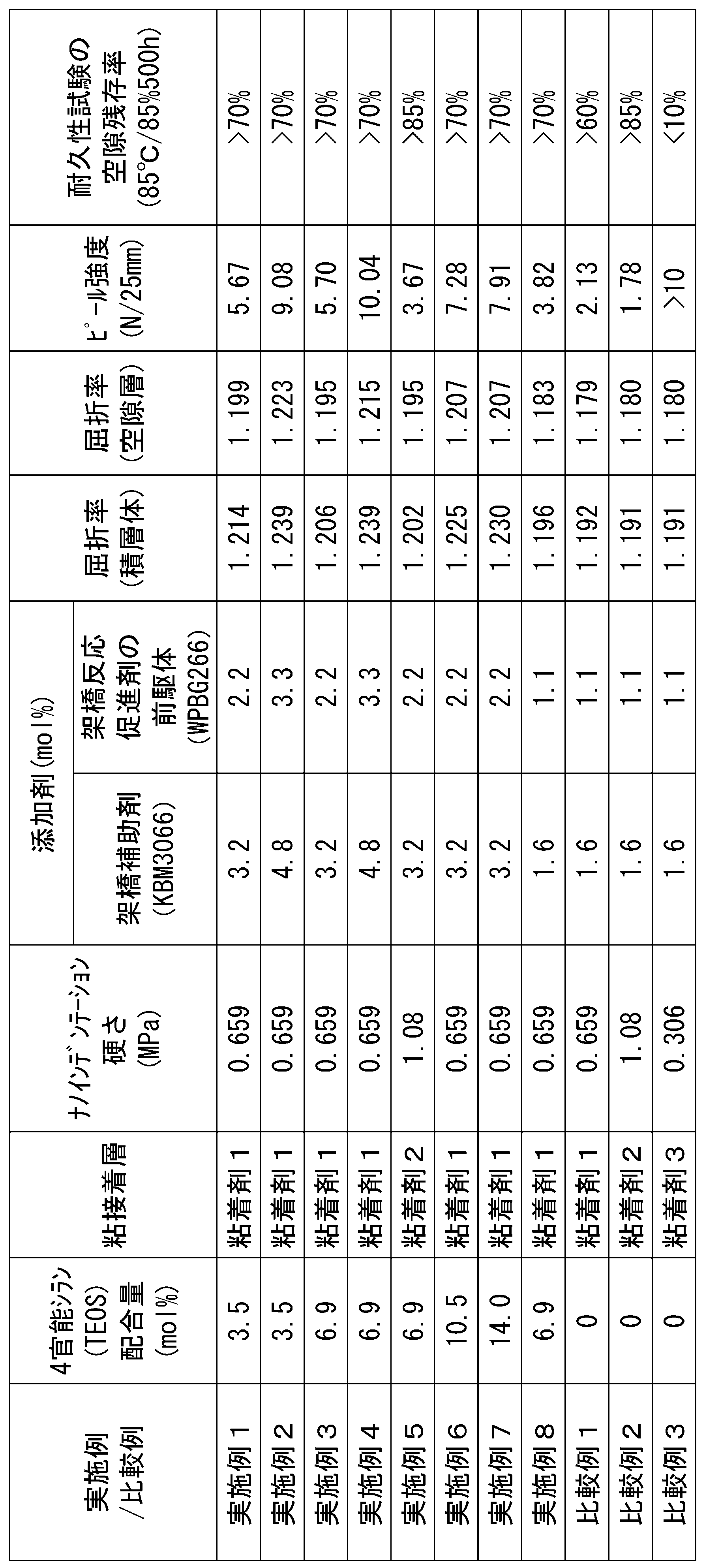
前記表1に示したとおり、実施例の空隙層を含む積層体は、層間のピール強度が3N/25mm以上であり、良好であった。一方で、比較例の積層体は、いずれも層間のピール強度が3N/25mm未満となった。
また、図4に、積層体とした際にナノインデンテーション硬さが0.5MPa以上となる実施例及び比較例の、ピール強度と屈折率の関係を示すグラフを示す。図4において、式「Y=136.4x-159.92」は、4官能シラン化合物を3官能シラン化合物に対して3.5mol%配合し、かつ、架橋補助剤及び架橋反応促進剤を発生する物質の添加量のみを変えた、実施例1、2の2点の平均をとった一次関数式である。式「Y=141.37x-165.06」は、4官能シラン化合物を3官能シラン化合物に対して6.9モル%配合し、かつ、架橋補助剤及び架橋反応促進剤を発生する物質の添加量のみを変えた、実施例3、4、8の3点の平均をとった一次関数式である。
図4のとおり、すべての実施例は、空隙層と粘接着層との層間のピール強度が3N/25mm以上となった。また、すべての実施例の空隙層は、実施形態記載の条件(1)(Y≧80X-93.8)を満たす結果となった。さらに、実施例の空隙層は、シラン化合物として4官能シラン化合物を含むことにより、同じ屈折率を有する4官能シラン化合物を含まない空隙層と比べて、ピール強度が大きくなることがわかった。すなわち、実施形態記載の条件(2)(Y≧100X-117)を満たす結果となった。また、架橋補助剤及び架橋反応促進剤(架橋反応促進剤の前駆体)の含有割合を増やすことで、よりピール強度が向上する結果となった。
本開示は、例えば、以下の付記のように記載することも可能である。ただし、以下の付記は例示であり、本開示はこれらの形態のみに限定されない。
(付記1)
空隙層であって、
前記空隙層は、ゲル状ケイ素化合物の粉砕物が化学的に結合している空隙層であり、
前記ゲル状ケイ素化合物は、シラン化合物が縮合又は部分的に縮合した化合物であり、
前記シラン化合物として、1~3官能シラン化合物及び4官能シラン化合物を含み、
前記空隙層の屈折率が、1.30以下である、
空隙層。
(付記2)
前記1~3官能シラン化合物の物質量に対する前記4官能シラン化合物の含有割合が、1~25mol%である、
付記1記載の空隙層。
(付記3)
前記空隙層が、添加剤の共存条件において前記ゲル状ケイ素化合物の粉砕物が化学的に結合した空隙層であり、
前記添加剤として、架橋反応促進剤及びその前駆体の少なくとも一方を含み、
前記前駆体が、光又は熱により前記架橋反応促進剤を発生する物質である、
付記1又は2記載の空隙層。
(付記4)
前記架橋反応促進剤が、酸性物質又は塩基性物質である、付記3記載の空隙層。
(付記5)
前記1~3官能シラン化合物及び前記4官能シラン化合物の合計の物質量に対して、前記架橋反応促進剤及びその前駆体の合計含有割合が、1mol%以上である、付記3又は4記載の空隙層。
(付記6)
前記空隙層が、添加剤の共存条件において前記ゲル状ケイ素化合物の粉砕物が化学的に結合した空隙層であり、
前記添加剤として、架橋補助剤を含む、
付記1から5のいずれかに記載の空隙層。
(付記7)
前記1~3官能シラン化合物及び前記4官能シラン化合物の合計の物質量に対して、前記架橋補助剤の合計含有割合が、1mol%以上である、付記6記載の空隙層。
(付記8)
空隙層であって、
前記空隙層は、添加剤の共存条件においてゲル状ケイ素化合物の粉砕物が化学的に結合している空隙層であり、
前記ゲル状ケイ素化合物は、シラン化合物が縮合又は部分的に縮合した化合物であり、
前記添加剤として、架橋反応促進剤及びその前駆体の少なくとも一方、並びに架橋補助剤を含み、
前記シラン化合物の合計の物質量に対して、
前記架橋反応促進剤及びその前駆体の合計含有割合が、1.5mol%以上であり、
前記架橋補助剤の合計含有割合が、2.0mol%以上であり、
前記空隙層の屈折率が、1.30以下である、
空隙層。
(付記9)
ゲル状シリカ合成工程、ゲル粉砕工程、及び結合工程を含み、
前記ゲル状シリカ合成工程は、シラン化合物を縮合又は部分的に縮合させてゲル状ケイ素化合物を合成する工程を含み、
前記シラン化合物は、1~3官能シラン化合物及び4官能シラン化合物を含み、
前記ゲル粉砕工程は、前記ゲル状ケイ素化合物を粉砕して粉砕物を得る工程を含み、
前記結合工程は、前記粉砕物を化学的に結合させる工程を含む、
空隙層の製造方法。
(付記10)
空隙層の製造方法であって、
ゲル状シリカ合成工程、ゲル粉砕工程、及び結合工程を含み、
前記ゲル状シリカ合成工程は、シラン化合物を縮合又は部分的に縮合させてゲル状ケイ素化合物を合成する工程を含み、
前記ゲル粉砕工程は、前記ゲル状ケイ素化合物を粉砕して粉砕物を得る工程を含み、
前記結合工程は、添加剤の共存条件において前記粉砕物を化学的に結合させる工程を含み、
前記添加剤として、架橋反応促進剤及びその前駆体の少なくとも一方、並びに架橋補助剤を含む、
空隙層の製造方法。
(付記11)
付記1から8のいずれかに記載の空隙層と、粘接着層とを含み、
前記粘接着層が、前記空隙層の片面又は両面に直接積層されている、積層体。
(付記12)
付記1から8のいずれかに記載の空隙層を含む、光学部材。
(付記13)
付記11記載の積層体を含む、光学部材。
(付記14)
付記12記載の光学部材を含む、光学装置。
(付記15)
画像表示装置、又は照明装置である、付記14記載の光学装置。
(付記16)
付記13記載の光学部材を含む、光学装置。
(付記17)
画像表示装置、又は照明装置である、付記16記載の光学装置。
空隙層であって、
前記空隙層は、ゲル状ケイ素化合物の粉砕物が化学的に結合している空隙層であり、
前記ゲル状ケイ素化合物は、シラン化合物が縮合又は部分的に縮合した化合物であり、
前記シラン化合物として、1~3官能シラン化合物及び4官能シラン化合物を含み、
前記空隙層の屈折率が、1.30以下である、
空隙層。
(付記2)
前記1~3官能シラン化合物の物質量に対する前記4官能シラン化合物の含有割合が、1~25mol%である、
付記1記載の空隙層。
(付記3)
前記空隙層が、添加剤の共存条件において前記ゲル状ケイ素化合物の粉砕物が化学的に結合した空隙層であり、
前記添加剤として、架橋反応促進剤及びその前駆体の少なくとも一方を含み、
前記前駆体が、光又は熱により前記架橋反応促進剤を発生する物質である、
付記1又は2記載の空隙層。
(付記4)
前記架橋反応促進剤が、酸性物質又は塩基性物質である、付記3記載の空隙層。
(付記5)
前記1~3官能シラン化合物及び前記4官能シラン化合物の合計の物質量に対して、前記架橋反応促進剤及びその前駆体の合計含有割合が、1mol%以上である、付記3又は4記載の空隙層。
(付記6)
前記空隙層が、添加剤の共存条件において前記ゲル状ケイ素化合物の粉砕物が化学的に結合した空隙層であり、
前記添加剤として、架橋補助剤を含む、
付記1から5のいずれかに記載の空隙層。
(付記7)
前記1~3官能シラン化合物及び前記4官能シラン化合物の合計の物質量に対して、前記架橋補助剤の合計含有割合が、1mol%以上である、付記6記載の空隙層。
(付記8)
空隙層であって、
前記空隙層は、添加剤の共存条件においてゲル状ケイ素化合物の粉砕物が化学的に結合している空隙層であり、
前記ゲル状ケイ素化合物は、シラン化合物が縮合又は部分的に縮合した化合物であり、
前記添加剤として、架橋反応促進剤及びその前駆体の少なくとも一方、並びに架橋補助剤を含み、
前記シラン化合物の合計の物質量に対して、
前記架橋反応促進剤及びその前駆体の合計含有割合が、1.5mol%以上であり、
前記架橋補助剤の合計含有割合が、2.0mol%以上であり、
前記空隙層の屈折率が、1.30以下である、
空隙層。
(付記9)
ゲル状シリカ合成工程、ゲル粉砕工程、及び結合工程を含み、
前記ゲル状シリカ合成工程は、シラン化合物を縮合又は部分的に縮合させてゲル状ケイ素化合物を合成する工程を含み、
前記シラン化合物は、1~3官能シラン化合物及び4官能シラン化合物を含み、
前記ゲル粉砕工程は、前記ゲル状ケイ素化合物を粉砕して粉砕物を得る工程を含み、
前記結合工程は、前記粉砕物を化学的に結合させる工程を含む、
空隙層の製造方法。
(付記10)
空隙層の製造方法であって、
ゲル状シリカ合成工程、ゲル粉砕工程、及び結合工程を含み、
前記ゲル状シリカ合成工程は、シラン化合物を縮合又は部分的に縮合させてゲル状ケイ素化合物を合成する工程を含み、
前記ゲル粉砕工程は、前記ゲル状ケイ素化合物を粉砕して粉砕物を得る工程を含み、
前記結合工程は、添加剤の共存条件において前記粉砕物を化学的に結合させる工程を含み、
前記添加剤として、架橋反応促進剤及びその前駆体の少なくとも一方、並びに架橋補助剤を含む、
空隙層の製造方法。
(付記11)
付記1から8のいずれかに記載の空隙層と、粘接着層とを含み、
前記粘接着層が、前記空隙層の片面又は両面に直接積層されている、積層体。
(付記12)
付記1から8のいずれかに記載の空隙層を含む、光学部材。
(付記13)
付記11記載の積層体を含む、光学部材。
(付記14)
付記12記載の光学部材を含む、光学装置。
(付記15)
画像表示装置、又は照明装置である、付記14記載の光学装置。
(付記16)
付記13記載の光学部材を含む、光学装置。
(付記17)
画像表示装置、又は照明装置である、付記16記載の光学装置。
以上、説明したとおり、本開示によれば、低屈折率であり、かつ、機械的強度に優れた空隙層、空隙層の製造方法、積層体、光学部材、及び光学装置を提供することができる。本開示の用途は特に限定されない。例えば、本開示の光学装置は、特に限定されず、画像表示装置、照明装置等があげられる。前記画像表示装置としては、例えば、液晶ディスプレイ、有機ELディスプレイ、マイクロLEDディスプレイ等があげられる。前記照明装置としては、例えば、有機EL照明等があげられる。さらに、本開示の積層体の用途は、本開示の光学部材及び光学装置に限定されず任意であり、広範な用途に使用可能である。
この出願は、2023年6月29日に出願された日本出願特願2023-107487を基礎とする優先権を主張し、その開示のすべてをここに取り込む。
10、10a、10b、10c、10d、10e 積層体
11 空隙層
12 粘接着層
13 中間層
14 基材
11 空隙層
12 粘接着層
13 中間層
14 基材
Claims (15)
- 空隙層であって、
前記空隙層は、ゲル状ケイ素化合物の粉砕物が化学的に結合している空隙層であり、
前記ゲル状ケイ素化合物は、シラン化合物が縮合又は部分的に縮合した化合物であり、
前記シラン化合物として、1~3官能シラン化合物及び4官能シラン化合物を含み、
前記空隙層の屈折率が、1.30以下である、
空隙層。 - 前記1~3官能シラン化合物の物質量に対する前記4官能シラン化合物の含有割合が、1~25mol%である、
請求項1記載の空隙層。 - 前記空隙層が、添加剤の共存条件において前記ゲル状ケイ素化合物の粉砕物が化学的に結合した空隙層であり、
前記添加剤として、架橋反応促進剤及びその前駆体の少なくとも一方を含み、
前記前駆体が、光又は熱により前記架橋反応促進剤を発生する物質である、
請求項1記載の空隙層。 - 前記架橋反応促進剤が、酸性物質又は塩基性物質である、請求項3記載の空隙層。
- 前記1~3官能シラン化合物及び前記4官能シラン化合物の合計の物質量に対して、前記架橋反応促進剤及びその前駆体の合計含有割合が、1mol%以上である、請求項3記載の空隙層。
- 前記空隙層が、添加剤の共存条件において前記ゲル状ケイ素化合物の粉砕物が化学的に結合した空隙層であり、
前記添加剤として、架橋補助剤を含む、
請求項1記載の空隙層。 - 前記1~3官能シラン化合物及び前記4官能シラン化合物の合計の物質量に対して、前記架橋補助剤の合計含有割合が、1mol%以上である、請求項6記載の空隙層。
- 空隙層であって、
前記空隙層は、添加剤の共存条件においてゲル状ケイ素化合物の粉砕物が化学的に結合している空隙層であり、
前記ゲル状ケイ素化合物は、シラン化合物が縮合又は部分的に縮合した化合物であり、
前記添加剤として、架橋反応促進剤及びその前駆体の少なくとも一方、並びに架橋補助剤を含み、
前記シラン化合物の合計の物質量に対して、
前記架橋反応促進剤及びその前駆体の合計含有割合が、1.5mol%以上であり、
前記架橋補助剤の合計含有割合が、2.0mol%以上であり、
前記空隙層の屈折率が、1.30以下である、
空隙層。 - ゲル状シリカ合成工程、ゲル粉砕工程、及び結合工程を含み、
前記ゲル状シリカ合成工程は、シラン化合物を縮合又は部分的に縮合させてゲル状ケイ素化合物を合成する工程を含み、
前記シラン化合物は、1~3官能シラン化合物及び4官能シラン化合物を含み、
前記ゲル粉砕工程は、前記ゲル状ケイ素化合物を粉砕して粉砕物を得る工程を含み、
前記結合工程は、前記粉砕物を化学的に結合させる工程を含む、
空隙層の製造方法。 - 空隙層の製造方法であって、
ゲル状シリカ合成工程、ゲル粉砕工程、及び結合工程を含み、
前記ゲル状シリカ合成工程は、シラン化合物を縮合又は部分的に縮合させてゲル状ケイ素化合物を合成する工程を含み、
前記ゲル粉砕工程は、前記ゲル状ケイ素化合物を粉砕して粉砕物を得る工程を含み、
前記結合工程は、添加剤の共存条件において前記粉砕物を化学的に結合させる工程を含み、
前記添加剤として、架橋反応促進剤及びその前駆体の少なくとも一方、並びに架橋補助剤を含む、
空隙層の製造方法。 - 請求項1から8のいずれか一項に記載の空隙層と、粘接着層とを含み、
前記粘接着層が、前記空隙層の片面又は両面に直接積層されている、積層体。 - 請求項1から8のいずれか一項に記載の空隙層を含む、光学部材。
- 請求項11記載の積層体を含む、光学部材。
- 請求項12記載の光学部材を含む、光学装置。
- 画像表示装置、又は照明装置である、請求項14記載の光学装置。
Priority Applications (4)
| Application Number | Priority Date | Filing Date | Title |
|---|---|---|---|
| CN202610086051.3A CN121975182A (zh) | 2023-06-29 | 2024-05-13 | 空隙层、空隙层的制造方法、层叠体、光学构件、及光学装置 |
| CN202480042829.XA CN121399504A (zh) | 2023-06-29 | 2024-05-13 | 空隙层、空隙层的制造方法、层叠体、光学构件、及光学装置 |
| KR1020257040764A KR20260030056A (ko) | 2023-06-29 | 2024-05-13 | 공극층, 공극층의 제조 방법, 적층체, 광학 부재, 및 광학 장치 |
| KR1020267009782A KR20260047651A (ko) | 2023-06-29 | 2024-05-13 | 공극층, 공극층의 제조 방법, 적층체, 광학 부재, 및 광학 장치 |
Applications Claiming Priority (2)
| Application Number | Priority Date | Filing Date | Title |
|---|---|---|---|
| JP2023-107487 | 2023-06-29 | ||
| JP2023107487A JP2025006592A (ja) | 2023-06-29 | 2023-06-29 | 空隙層、空隙層の製造方法、積層体、光学部材、及び光学装置 |
Publications (1)
| Publication Number | Publication Date |
|---|---|
| WO2025004563A1 true WO2025004563A1 (ja) | 2025-01-02 |
Family
ID=93938100
Family Applications (1)
| Application Number | Title | Priority Date | Filing Date |
|---|---|---|---|
| PCT/JP2024/017667 Ceased WO2025004563A1 (ja) | 2023-06-29 | 2024-05-13 | 空隙層、空隙層の製造方法、積層体、光学部材、及び光学装置 |
Country Status (5)
| Country | Link |
|---|---|
| JP (2) | JP2025006592A (ja) |
| KR (2) | KR20260047651A (ja) |
| CN (2) | CN121975182A (ja) |
| TW (2) | TW202513472A (ja) |
| WO (1) | WO2025004563A1 (ja) |
Citations (4)
| Publication number | Priority date | Publication date | Assignee | Title |
|---|---|---|---|---|
| JP2017069003A (ja) * | 2015-09-29 | 2017-04-06 | 日東電工株式会社 | フレキシブル発光デバイス、照明装置および画像表示装置 |
| JP2018123233A (ja) * | 2017-01-31 | 2018-08-09 | 日東電工株式会社 | 空隙層、空隙層含有粘接着シート、空隙層の製造方法、空隙層含有粘接着シートの製造方法、および光学デバイス |
| JP2019064259A (ja) * | 2017-09-29 | 2019-04-25 | 日東電工株式会社 | 積層体、光学部材および光学装置 |
| WO2021193591A1 (ja) * | 2020-03-24 | 2021-09-30 | 日東電工株式会社 | 両面粘着剤層付光学積層体および光学装置 |
-
2023
- 2023-06-29 JP JP2023107487A patent/JP2025006592A/ja active Pending
-
2024
- 2024-05-13 CN CN202610086051.3A patent/CN121975182A/zh active Pending
- 2024-05-13 CN CN202480042829.XA patent/CN121399504A/zh active Pending
- 2024-05-13 KR KR1020267009782A patent/KR20260047651A/ko active Pending
- 2024-05-13 KR KR1020257040764A patent/KR20260030056A/ko active Pending
- 2024-05-13 WO PCT/JP2024/017667 patent/WO2025004563A1/ja not_active Ceased
- 2024-06-19 TW TW113122660A patent/TW202513472A/zh unknown
- 2024-06-19 TW TW114150090A patent/TW202615347A/zh unknown
-
2025
- 2025-11-05 JP JP2025186597A patent/JP2026015375A/ja active Pending
Patent Citations (4)
| Publication number | Priority date | Publication date | Assignee | Title |
|---|---|---|---|---|
| JP2017069003A (ja) * | 2015-09-29 | 2017-04-06 | 日東電工株式会社 | フレキシブル発光デバイス、照明装置および画像表示装置 |
| JP2018123233A (ja) * | 2017-01-31 | 2018-08-09 | 日東電工株式会社 | 空隙層、空隙層含有粘接着シート、空隙層の製造方法、空隙層含有粘接着シートの製造方法、および光学デバイス |
| JP2019064259A (ja) * | 2017-09-29 | 2019-04-25 | 日東電工株式会社 | 積層体、光学部材および光学装置 |
| WO2021193591A1 (ja) * | 2020-03-24 | 2021-09-30 | 日東電工株式会社 | 両面粘着剤層付光学積層体および光学装置 |
Also Published As
| Publication number | Publication date |
|---|---|
| TW202615347A (zh) | 2026-04-16 |
| KR20260047651A (ko) | 2026-04-08 |
| KR20260030056A (ko) | 2026-03-05 |
| TW202513472A (zh) | 2025-04-01 |
| CN121399504A (zh) | 2026-01-23 |
| JP2025006592A (ja) | 2025-01-17 |
| CN121975182A (zh) | 2026-05-05 |
| JP2026015375A (ja) | 2026-01-29 |
Similar Documents
| Publication | Publication Date | Title |
|---|---|---|
| US11396614B2 (en) | Void-containing layer, laminate, method for producing void-containing layer, optical member, and optical apparatus | |
| KR102477728B1 (ko) | 실리콘 다공체 및 그 제조 방법 | |
| US11402569B2 (en) | Optical sheet for light guide plate type liquid crystal display, backlight unit for light guide plate type liquid crystal display, and light guide plate type liquid crystal display | |
| JP7182358B2 (ja) | 低屈折率層含有粘接着シート、低屈折率層含有粘接着シートの製造方法、および光学デバイス | |
| JP7662735B2 (ja) | 積層体、光学部材および光学装置 | |
| TWI871274B (zh) | 積層體、光學構件及光學裝置 | |
| JP6563750B2 (ja) | 塗料およびその製造方法 | |
| TWI876001B (zh) | 雙面附黏著劑層之光學積層體及光學裝置 | |
| WO2018142813A1 (ja) | 低屈折率層含有粘接着シート、低屈折率層含有粘接着シートの製造方法、および光学デバイス | |
| US20260116040A1 (en) | Laminate, optical member, and optical device | |
| JP2025006592A (ja) | 空隙層、空隙層の製造方法、積層体、光学部材、及び光学装置 | |
| WO2016104765A1 (ja) | 塗料およびその製造方法 | |
| JP2020073629A (ja) | 空隙層、積層体、空隙層の製造方法、光学部材および光学装置 | |
| JP7729730B2 (ja) | 光学積層体、光学積層体の製造方法、光学部材、光学装置、光学部材の製造方法、及び光学装置の製造方法 |
Legal Events
| Date | Code | Title | Description |
|---|---|---|---|
| 121 | Ep: the epo has been informed by wipo that ep was designated in this application |
Ref document number: 24831436 Country of ref document: EP Kind code of ref document: A1 |
|
| NENP | Non-entry into the national phase |
Ref country code: DE |
|
| 122 | Ep: pct application non-entry in european phase |
Ref document number: 24831436 Country of ref document: EP Kind code of ref document: A1 |