WO2025004543A1 - 半導体装置 - Google Patents
半導体装置 Download PDFInfo
- Publication number
- WO2025004543A1 WO2025004543A1 PCT/JP2024/017093 JP2024017093W WO2025004543A1 WO 2025004543 A1 WO2025004543 A1 WO 2025004543A1 JP 2024017093 W JP2024017093 W JP 2024017093W WO 2025004543 A1 WO2025004543 A1 WO 2025004543A1
- Authority
- WO
- WIPO (PCT)
- Prior art keywords
- trench
- region
- electric field
- impurity region
- semiconductor device
- Prior art date
- Legal status (The legal status is an assumption and is not a legal conclusion. Google has not performed a legal analysis and makes no representation as to the accuracy of the status listed.)
- Ceased
Links
Images









Classifications
-
- H—ELECTRICITY
- H10—SEMICONDUCTOR DEVICES; ELECTRIC SOLID-STATE DEVICES NOT OTHERWISE PROVIDED FOR
- H10D—INORGANIC ELECTRIC SEMICONDUCTOR DEVICES
- H10D62/00—Semiconductor bodies, or regions thereof, of devices having potential barriers
- H10D62/40—Crystalline structures
- H10D62/405—Orientations of crystalline planes
-
- H—ELECTRICITY
- H10—SEMICONDUCTOR DEVICES; ELECTRIC SOLID-STATE DEVICES NOT OTHERWISE PROVIDED FOR
- H10D—INORGANIC ELECTRIC SEMICONDUCTOR DEVICES
- H10D12/00—Bipolar devices controlled by the field effect, e.g. insulated-gate bipolar transistors [IGBT]
- H10D12/01—Manufacture or treatment
- H10D12/031—Manufacture or treatment of IGBTs
-
- H—ELECTRICITY
- H10—SEMICONDUCTOR DEVICES; ELECTRIC SOLID-STATE DEVICES NOT OTHERWISE PROVIDED FOR
- H10D—INORGANIC ELECTRIC SEMICONDUCTOR DEVICES
- H10D12/00—Bipolar devices controlled by the field effect, e.g. insulated-gate bipolar transistors [IGBT]
- H10D12/01—Manufacture or treatment
- H10D12/031—Manufacture or treatment of IGBTs
- H10D12/032—Manufacture or treatment of IGBTs of vertical IGBTs
- H10D12/038—Manufacture or treatment of IGBTs of vertical IGBTs having a recessed gate, e.g. trench-gate IGBTs
-
- H—ELECTRICITY
- H10—SEMICONDUCTOR DEVICES; ELECTRIC SOLID-STATE DEVICES NOT OTHERWISE PROVIDED FOR
- H10D—INORGANIC ELECTRIC SEMICONDUCTOR DEVICES
- H10D12/00—Bipolar devices controlled by the field effect, e.g. insulated-gate bipolar transistors [IGBT]
- H10D12/411—Insulated-gate bipolar transistors [IGBT]
- H10D12/415—Insulated-gate bipolar transistors [IGBT] having edge termination structures
-
- H—ELECTRICITY
- H10—SEMICONDUCTOR DEVICES; ELECTRIC SOLID-STATE DEVICES NOT OTHERWISE PROVIDED FOR
- H10D—INORGANIC ELECTRIC SEMICONDUCTOR DEVICES
- H10D12/00—Bipolar devices controlled by the field effect, e.g. insulated-gate bipolar transistors [IGBT]
- H10D12/411—Insulated-gate bipolar transistors [IGBT]
- H10D12/441—Vertical IGBTs
- H10D12/461—Vertical IGBTs having non-planar surfaces, e.g. having trenches, recesses or pillars in the surfaces of the emitter, base or collector regions
- H10D12/481—Vertical IGBTs having non-planar surfaces, e.g. having trenches, recesses or pillars in the surfaces of the emitter, base or collector regions having gate structures on slanted surfaces, on vertical surfaces, or in grooves, e.g. trench gate IGBTs
-
- H—ELECTRICITY
- H10—SEMICONDUCTOR DEVICES; ELECTRIC SOLID-STATE DEVICES NOT OTHERWISE PROVIDED FOR
- H10D—INORGANIC ELECTRIC SEMICONDUCTOR DEVICES
- H10D30/00—Field-effect transistors [FET]
- H10D30/60—Insulated-gate field-effect transistors [IGFET]
- H10D30/64—Double-diffused metal-oxide semiconductor [DMOS] FETs
- H10D30/66—Vertical DMOS [VDMOS] FETs
- H10D30/665—Vertical DMOS [VDMOS] FETs having edge termination structures
-
- H—ELECTRICITY
- H10—SEMICONDUCTOR DEVICES; ELECTRIC SOLID-STATE DEVICES NOT OTHERWISE PROVIDED FOR
- H10D—INORGANIC ELECTRIC SEMICONDUCTOR DEVICES
- H10D30/00—Field-effect transistors [FET]
- H10D30/60—Insulated-gate field-effect transistors [IGFET]
- H10D30/64—Double-diffused metal-oxide semiconductor [DMOS] FETs
- H10D30/66—Vertical DMOS [VDMOS] FETs
- H10D30/668—Vertical DMOS [VDMOS] FETs having trench gate electrodes, e.g. UMOS transistors
-
- H—ELECTRICITY
- H10—SEMICONDUCTOR DEVICES; ELECTRIC SOLID-STATE DEVICES NOT OTHERWISE PROVIDED FOR
- H10D—INORGANIC ELECTRIC SEMICONDUCTOR DEVICES
- H10D62/00—Semiconductor bodies, or regions thereof, of devices having potential barriers
- H10D62/10—Shapes, relative sizes or dispositions of the regions of the semiconductor bodies; Shapes of the semiconductor bodies
- H10D62/102—Constructional design considerations for preventing surface leakage or controlling electric field concentration
- H10D62/103—Constructional design considerations for preventing surface leakage or controlling electric field concentration for increasing or controlling the breakdown voltage of reverse-biased devices
- H10D62/105—Constructional design considerations for preventing surface leakage or controlling electric field concentration for increasing or controlling the breakdown voltage of reverse-biased devices by having particular doping profiles, shapes or arrangements of PN junctions; by having supplementary regions, e.g. junction termination extension [JTE]
- H10D62/106—Constructional design considerations for preventing surface leakage or controlling electric field concentration for increasing or controlling the breakdown voltage of reverse-biased devices by having particular doping profiles, shapes or arrangements of PN junctions; by having supplementary regions, e.g. junction termination extension [JTE] having supplementary regions doped oppositely to or in rectifying contact with regions of the semiconductor bodies, e.g. guard rings with PN or Schottky junctions
-
- H—ELECTRICITY
- H10—SEMICONDUCTOR DEVICES; ELECTRIC SOLID-STATE DEVICES NOT OTHERWISE PROVIDED FOR
- H10D—INORGANIC ELECTRIC SEMICONDUCTOR DEVICES
- H10D62/00—Semiconductor bodies, or regions thereof, of devices having potential barriers
- H10D62/10—Shapes, relative sizes or dispositions of the regions of the semiconductor bodies; Shapes of the semiconductor bodies
- H10D62/102—Constructional design considerations for preventing surface leakage or controlling electric field concentration
- H10D62/103—Constructional design considerations for preventing surface leakage or controlling electric field concentration for increasing or controlling the breakdown voltage of reverse-biased devices
- H10D62/105—Constructional design considerations for preventing surface leakage or controlling electric field concentration for increasing or controlling the breakdown voltage of reverse-biased devices by having particular doping profiles, shapes or arrangements of PN junctions; by having supplementary regions, e.g. junction termination extension [JTE]
- H10D62/106—Constructional design considerations for preventing surface leakage or controlling electric field concentration for increasing or controlling the breakdown voltage of reverse-biased devices by having particular doping profiles, shapes or arrangements of PN junctions; by having supplementary regions, e.g. junction termination extension [JTE] having supplementary regions doped oppositely to or in rectifying contact with regions of the semiconductor bodies, e.g. guard rings with PN or Schottky junctions
- H10D62/107—Buried supplementary regions, e.g. buried guard rings
-
- H—ELECTRICITY
- H10—SEMICONDUCTOR DEVICES; ELECTRIC SOLID-STATE DEVICES NOT OTHERWISE PROVIDED FOR
- H10D—INORGANIC ELECTRIC SEMICONDUCTOR DEVICES
- H10D62/00—Semiconductor bodies, or regions thereof, of devices having potential barriers
- H10D62/10—Shapes, relative sizes or dispositions of the regions of the semiconductor bodies; Shapes of the semiconductor bodies
- H10D62/102—Constructional design considerations for preventing surface leakage or controlling electric field concentration
- H10D62/103—Constructional design considerations for preventing surface leakage or controlling electric field concentration for increasing or controlling the breakdown voltage of reverse-biased devices
- H10D62/105—Constructional design considerations for preventing surface leakage or controlling electric field concentration for increasing or controlling the breakdown voltage of reverse-biased devices by having particular doping profiles, shapes or arrangements of PN junctions; by having supplementary regions, e.g. junction termination extension [JTE]
- H10D62/109—Reduced surface field [RESURF] PN junction structures
-
- H—ELECTRICITY
- H10—SEMICONDUCTOR DEVICES; ELECTRIC SOLID-STATE DEVICES NOT OTHERWISE PROVIDED FOR
- H10D—INORGANIC ELECTRIC SEMICONDUCTOR DEVICES
- H10D62/00—Semiconductor bodies, or regions thereof, of devices having potential barriers
- H10D62/10—Shapes, relative sizes or dispositions of the regions of the semiconductor bodies; Shapes of the semiconductor bodies
- H10D62/124—Shapes, relative sizes or dispositions of the regions of semiconductor bodies or of junctions between the regions
- H10D62/126—Top-view geometrical layouts of the regions or the junctions
- H10D62/127—Top-view geometrical layouts of the regions or the junctions of cellular field-effect devices, e.g. multicellular DMOS transistors or IGBTs
-
- H—ELECTRICITY
- H10—SEMICONDUCTOR DEVICES; ELECTRIC SOLID-STATE DEVICES NOT OTHERWISE PROVIDED FOR
- H10D—INORGANIC ELECTRIC SEMICONDUCTOR DEVICES
- H10D62/00—Semiconductor bodies, or regions thereof, of devices having potential barriers
- H10D62/10—Shapes, relative sizes or dispositions of the regions of the semiconductor bodies; Shapes of the semiconductor bodies
- H10D62/13—Semiconductor regions connected to electrodes carrying current to be rectified, amplified or switched, e.g. source or drain regions
- H10D62/149—Source or drain regions of field-effect devices
- H10D62/151—Source or drain regions of field-effect devices of IGFETs
- H10D62/156—Drain regions of DMOS transistors
- H10D62/157—Impurity concentrations or distributions
-
- H—ELECTRICITY
- H10—SEMICONDUCTOR DEVICES; ELECTRIC SOLID-STATE DEVICES NOT OTHERWISE PROVIDED FOR
- H10D—INORGANIC ELECTRIC SEMICONDUCTOR DEVICES
- H10D62/00—Semiconductor bodies, or regions thereof, of devices having potential barriers
- H10D62/10—Shapes, relative sizes or dispositions of the regions of the semiconductor bodies; Shapes of the semiconductor bodies
- H10D62/17—Semiconductor regions connected to electrodes not carrying current to be rectified, amplified or switched, e.g. channel regions
- H10D62/393—Body regions of DMOS transistors or IGBTs
-
- H—ELECTRICITY
- H10—SEMICONDUCTOR DEVICES; ELECTRIC SOLID-STATE DEVICES NOT OTHERWISE PROVIDED FOR
- H10D—INORGANIC ELECTRIC SEMICONDUCTOR DEVICES
- H10D62/00—Semiconductor bodies, or regions thereof, of devices having potential barriers
- H10D62/80—Semiconductor bodies, or regions thereof, of devices having potential barriers characterised by the materials
- H10D62/83—Semiconductor bodies, or regions thereof, of devices having potential barriers characterised by the materials being Group IV materials, e.g. B-doped Si or undoped Ge
- H10D62/832—Semiconductor bodies, or regions thereof, of devices having potential barriers characterised by the materials being Group IV materials, e.g. B-doped Si or undoped Ge being Group IV materials comprising two or more elements, e.g. SiGe
- H10D62/8325—Silicon carbide
Definitions
- the first direction X is the m-axis direction ([1-100] direction) of the SiC single crystal
- the second direction Y is the a-axis direction ([11-20] direction) of the SiC single crystal.
- the first direction X may be the a-axis direction of the SiC single crystal
- the second direction Y may be the m-axis direction of the SiC single crystal.
- the chip 2 (first main surface 3 and second main surface 4) has an off angle ⁇ o that is inclined at a predetermined angle in a predetermined off direction Do with respect to the c-plane of the SiC single crystal.
- the c-axis ((0001) axis) of the SiC single crystal is inclined by the off angle ⁇ o from the vertical axis toward the off direction Do.
- the c-plane of the SiC single crystal is inclined by the off angle ⁇ o with respect to the horizontal plane.
- the off-direction Do is preferably the a-axis direction of the SiC single crystal (i.e., the second direction Y).
- the off-angle ⁇ o may be greater than 0° and less than or equal to 10°.
- the off-angle ⁇ o may have a value that falls within any one of the following ranges: greater than 0° and less than or equal to 1°, 1° or more and less than or equal to 2.5°, 2.5° or more and less than or equal to 5°, 5° or more and less than or equal to 7.5°, and 7.5° or more and less than or equal to 10°.
- the semiconductor layer 7 includes an n-type drift region 8.
- the drift region 8 is formed by a portion (n-type portion) of the semiconductor layer 7. More specifically, the drift region 8 is formed by a portion of the semiconductor layer 7 on the second main surface 4 side relative to the body region 15 (described later) and the electric field relaxation structure 21 (described later) in the vertical direction Z.
- the boundary between the base layer 6 and the semiconductor layer 7 is not necessarily visible, but can be indirectly evaluated and/or determined from other configurations and elements.
- the semiconductor layer 7 has an off-direction Do and an off-angle ⁇ o that are approximately the same as the off-direction Do and off-angle ⁇ o of the base layer 6.
- the n-type impurity concentration of the semiconductor layer 7 (drift region 8) is preferably lower than the n-type impurity concentration of the base layer 6.
- the semiconductor layer 7 may have a peak n-type impurity concentration of 1 ⁇ 10 15 cm -3 or more and 1 ⁇ 10 18 cm -3 or less.
- the n-type impurity concentration of the semiconductor layer 7 may be approximately constant in the thickness direction.
- the n-type impurity concentration of the semiconductor layer 7 may have a concentration gradient that gradually increases and/or gradually decreases in the stacking direction (crystal growth direction).
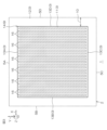
- the semiconductor device 1 includes a peripheral region 10 that is set outside the active region 9 in the chip 2.
- the peripheral region 10 is provided in a region between the periphery of the chip 2 and the active region 9 in a planar view.
- the peripheral region 10 extends in a band shape along the active region 9 in a planar view, and is set in a polygonal ring shape (a square ring in this embodiment) that surrounds the active region 9.
- the active surface 11 may be referred to as the "first surface portion,” the outer peripheral surface 12 as the “second surface portion,” the first to fourth connection surfaces 13A to 13D as the “connection surface portion,” and the active plateau 14 as the “active mesa portion.”
- the active surface 11, the outer peripheral surface 12, and the first to fourth connection surfaces 13A to 13D may be considered to be components of the chip 2 (first main surface 3).
- the active surface 11 is formed in the active region 9. That is, the active surface 11 is formed at a distance inward from the periphery (first to fourth side surfaces 5A to 5D) of the first main surface 3.
- the active surface 11 has a flat surface extending in the first direction X and the second direction Y.
- the active surface 11 is formed by a c-plane (Si-plane).
- the active surface 11 is formed in a quadrangle shape having four sides parallel to the first to fourth side surfaces 5A to 5D in a plan view.
- the outer peripheral surface 12 is formed in the outer peripheral region 10. That is, the outer peripheral surface 12 is formed outside the active surface 11.
- the outer peripheral surface 12 is recessed in the thickness direction of the chip 2 (towards the second main surface 4) relative to the active surface 11. Specifically, in this embodiment, the outer peripheral surface 12 is recessed to a depth less than the thickness of the semiconductor layer 7 so as to expose the semiconductor layer 7. That is, the outer peripheral surface 12 faces the base layer 6 with a portion of the semiconductor layer 7 in between, exposing the semiconductor layer 7.
- the outer peripheral surface 12 extends in a band shape along the active surface 11 in a plan view, and is formed in a ring shape (specifically, a square ring shape) surrounding the active surface 11.
- the outer peripheral surface 12 has a flat surface extending in the first direction X and the second direction Y, and is formed approximately parallel to the active surface 11.
- the outer peripheral surface 12 is formed by a c-plane (Si-plane).
- the outer peripheral surface 12 is connected to the first to fourth side surfaces 5A to 5D.
- the outer peripheral surface 12 has an outer peripheral depth DO.
- the outer peripheral depth DO may be 0.1 ⁇ m or more and 2 ⁇ m or less.
- the outer peripheral depth DO may have a value that falls within any one of the following ranges: 0.1 ⁇ m or more and 0.25 ⁇ m or less, 0.25 ⁇ m or more and 0.5 ⁇ m or less, 0.5 ⁇ m or more and 0.75 ⁇ m or less, 0.75 ⁇ m or more and 1 ⁇ m or less, 1 ⁇ m or more and 1.5 ⁇ m or less, and 1.5 ⁇ m or more and 2 ⁇ m or less.
- the outer peripheral depth DO is preferably 0.1 ⁇ m or more and 1.5 ⁇ m or less.
- the first to fourth connection surfaces 13A to 13D extend in the vertical direction Z and connect the active surface 11 and the outer peripheral surface 12.
- the first connection surface 13A is located on the first side surface 5A side
- the second connection surface 13B is located on the second side surface 5B side
- the third connection surface 13C is located on the third side surface 5C side
- the fourth connection surface 13D is located on the fourth side surface 5D side.
- the first connection surface 13A and the third connection surface 13C extend in the first direction X and face the second direction Y.
- the second connection surface 13B and the fourth connection surface 13D extend in the second direction Y and face the first direction X.
- the first to fourth connection surfaces 13A to 13D may extend approximately vertically between the active surface 11 and the outer peripheral surface 12 so as to define a quadrangular prism-shaped active plateau 14.
- the first to fourth connection surfaces 13A to 13D may be inclined obliquely downward from the active surface 11 toward the outer peripheral surface 12 so as to define a quadrangular pyramid-shaped active plateau 14.
- the active plateau 14 is defined in a protruding shape on the semiconductor layer 7 at the first main surface 3.
- the active plateau 14 is formed only on the semiconductor layer 7, and is not formed on the base layer 6.
- the body region 15 may have a peak p-type impurity concentration of 1 ⁇ 10 15 cm ⁇ 3 or more and 1 ⁇ 10 18 cm ⁇ 3 or less.
- the p-type impurity concentration of the body region 15 is preferably adjusted by at least one trivalent element.
- the trivalent element of the body region 15 may be at least one of boron, aluminum, gallium, and indium.
- the semiconductor device 1 includes a plurality of trench electrode type trench structures 16 formed on the first main surface 3 (active surface 11) in the active region 9.
- the trench structures 16 may be referred to as "gate structures", “trench gate structures”, etc.
- a gate potential is applied to the plurality of trench structures 16 as a control potential.
- the plurality of trench structures 16 control the inversion and non-inversion of the channel (current path) in the body region 15 in response to the gate potential.
- the multiple trench structures 16 are arranged at intervals inward from the periphery (first to fourth connection surfaces 13A to 13D) of the active surface 11 in the active region 9.
- the multiple trench structures 16 are arranged at intervals in the first direction X, and are each formed in a strip shape extending in the second direction Y.
- the multiple trench structures 16 are arranged at intervals in the m-axis direction and each extends in the a-axis direction.
- the multiple trench structures 16 are arranged in stripes extending in the a-axis direction (second direction Y).
- the extension direction of the multiple trench structures 16 coincides with the off-direction Do of the semiconductor layer 7.
- the multiple trench structures 16 are formed at intervals from the lower end (base layer 6) of the semiconductor layer 7 toward the first main surface 3 (active surface 11), and face the base layer 6 with a portion of the semiconductor layer 7 in between.
- the multiple trench structures 16 define a lower region 7a in the region between the bottom walls of the multiple trench structures 16 and the lower end (base layer 6) of the semiconductor layer 7.
- Each trench structure 16 has a trench width WT in the arrangement direction and a trench depth DT in the vertical direction Z.
- the trench width WT is preferably less than the second thickness T2 of the semiconductor layer 7.
- the trench width WT may be 0.1 ⁇ m or more and 5 ⁇ m or less.
- the trench width WT may have a value falling within any one of the following ranges: 0.1 ⁇ m to 0.25 ⁇ m, 0.25 ⁇ m to 0.5 ⁇ m, 0.5 ⁇ m to 0.75 ⁇ m, 0.75 ⁇ m to 1 ⁇ m, 1 ⁇ m to 1.5 ⁇ m, 1.5 ⁇ m to 2 ⁇ m, 2 ⁇ m to 2.5 ⁇ m, 2.5 ⁇ m to 3 ⁇ m, 3 ⁇ m to 3.5 ⁇ m, 3.5 ⁇ m to 4 ⁇ m, 4 ⁇ m to 4.5 ⁇ m, and 4.5 ⁇ m to 5 ⁇ m.
- the trench depth DT is preferably less than the second thickness T2 of the semiconductor layer 7. It is particularly preferable that the trench depth DT is approximately equal to the aforementioned outer periphery depth DO. Of course, the trench depth DT may be greater than or less than the outer periphery depth DO.
- the trench depth DT is preferably greater than the trench width WT.
- each of the multiple trench structures 16 has an aspect ratio DT/WT that extends in a vertically elongated columnar shape.
- the aspect ratio DT/WT is the ratio of the trench width WT to the trench depth DT.
- the trench depth DT may be 0.1 ⁇ m or more and 5 ⁇ m or less.
- the trench depth DT may have a value in any one of the following ranges: 0.1 ⁇ m to 0.25 ⁇ m, 0.25 ⁇ m to 0.5 ⁇ m, 0.5 ⁇ m to 1 ⁇ m, 1 ⁇ m to 1.5 ⁇ m, 1.5 ⁇ m to 2 ⁇ m, 2 ⁇ m to 3 ⁇ m, 3 ⁇ m to 4 ⁇ m, and 4 ⁇ m to 5 ⁇ m.
- the trench depth DT is preferably 0.1 ⁇ m to 1.5 ⁇ m, and more preferably 0.5 ⁇ m to 1.5 ⁇ m.
- the multiple trench structures 16 are arranged in the first direction X at intervals of the trench pitch PT.
- the trench pitch PT is preferably less than the second thickness T2 of the semiconductor layer 7.
- the trench pitch PT is preferably less than the trench depth DT.
- the trench pitch PT may be 0.1 ⁇ m or more and 5 ⁇ m or less.
- the trench pitch PT may have a value in any one of the ranges of 0.1 ⁇ m to 0.25 ⁇ m, 0.25 ⁇ m to 0.5 ⁇ m, 0.5 ⁇ m to 0.75 ⁇ m, 0.75 ⁇ m to 1 ⁇ m, 1 ⁇ m to 1.5 ⁇ m, 1.5 ⁇ m to 2 ⁇ m, 2 ⁇ m to 2.5 ⁇ m, 2.5 ⁇ m to 3 ⁇ m, 3 ⁇ m to 3.5 ⁇ m, 3.5 ⁇ m to 4 ⁇ m, 4 ⁇ m to 4.5 ⁇ m, and 4.5 ⁇ m to 5 ⁇ m.
- the trench pitch PT is preferably 0.5 ⁇ m to 3 ⁇ m, and more preferably 0.5 ⁇ m to 1.5 ⁇ m.
- Each trench structure 16 includes a trench 17, an insulating film 18, and a buried electrode 19.
- the trench 17 is formed in the active surface 11 and defines the walls (side walls and bottom wall) of the trench structure 16.
- the bottom wall of the trench 17 preferably has a flat portion.
- a mesa portion 20 formed by a part of the semiconductor layer 7 is formed between adjacent trenches 17.
- the mesa portion 20 may be referred to as an "element mesa portion.”
- the multiple trenches 17 and multiple mesa portions 20 are in the form of stripes extending along the second direction Y, and are arranged alternately in the first direction X.
- the multiple trenches 17 and multiple mesa portions 20 are arranged in a stripe pattern as a whole.
- the flat portion of the bottom wall of trench 17 extends approximately parallel to first main surface 3.
- the bottom wall of trench 17 has an off angle ⁇ o that is inclined at a predetermined angle in a predetermined off direction Do relative to the c-plane.
- the bottom wall of trench 17 has a flat portion that extends in the off direction Do.
- the bottom wall of trench 17 may be curved in an arc shape toward the lower end side of semiconductor layer 7.
- the insulating film 18 covers the wall surface of the trench 17.
- the insulating film 18 may include at least one of a silicon oxide film, a silicon nitride film, and a silicon oxynitride film.
- the insulating film 18 has a single-layer structure made of a silicon oxide film. It is particularly preferable that the insulating film 18 includes a silicon oxide film made of an oxide of the chip 2.
- the buried electrode 19 is buried in the trench 17 and faces the channel across the insulating film 18. In this embodiment, the buried electrode 19 faces the body region 15 across the insulating film 18.
- the buried electrode 19 may include p-type or n-type conductive polysilicon.
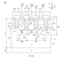
- the semiconductor device 1 includes a plurality of p-type electric field relaxation structures 21 formed at intervals in the horizontal direction in the semiconductor layer 7. Specifically, the plurality of electric field relaxation structures 21 are formed in the mesa portion 20 and the lower region 7a in the semiconductor layer 7. The plurality of electric field relaxation structures 21 are formed in the thickness range between the lower end of the semiconductor layer 7 and the bottom walls of the plurality of trench structures 16.
- the electric field relaxation structures 21 are arranged at intervals in the first direction X in the lower region 7a, and are each formed in a strip shape extending in the second direction Y. In other words, the electric field relaxation structures 21 are arranged at intervals in the m-axis direction and extend in the a-axis direction of the SiC single crystal. The electric field relaxation structures 21 are formed in stripes extending in the a-axis direction (second direction Y), and the extension direction of the electric field relaxation structures 21 coincides with the off-direction Do of the semiconductor layer 7.
- the electric field relaxation structures 21 are arranged at intervals of the relaxation pitch PR in the first direction X. It is preferable that the relaxation pitch PR is at least twice the trench pitch PT.
- the relaxation pitch PR may have a value in any one of the following ranges: 0.25 ⁇ m to 0.5 ⁇ m, 0.5 ⁇ m to 0.75 ⁇ m, 0.75 ⁇ m to 1 ⁇ m, 1 ⁇ m to 1.5 ⁇ m, 1.5 ⁇ m to 2 ⁇ m, 2 ⁇ m to 2.5 ⁇ m, 2.5 ⁇ m to 3 ⁇ m, 3 ⁇ m to 3.5 ⁇ m, 3.5 ⁇ m to 4 ⁇ m, 4 ⁇ m to 4.5 ⁇ m, and 4.5 ⁇ m to 5 ⁇ m.
- the relaxation pitch PR is preferably 2.5 ⁇ m to 3 ⁇ m.
- the trench pitch PT is preferably 0.5 ⁇ m to 1.5 ⁇ m.
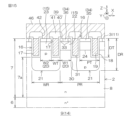
- Each electric field relaxation structure 21 is formed integrally with the body region 15 and spans the bottom walls of multiple trenches 17.
- each electric field relaxation structure 21 extends from the body region 15 sandwiched between two adjacent trenches 17 downward in the vertical direction Z below the bottom walls of the trenches 17, and spreads in the horizontal direction along the first main surface 3, overlapping the bottom walls of the trenches 17 on both sides.
- Each electric field relaxation structure 21 covers the bottom wall of the trench 17.
- each electric field relaxation structure 21 forms at least a part of each of the side walls and bottom walls of the trench 17, and is in contact with the insulating film 18.
- Each electric field relaxation structure 21 has a substantially L-shaped exposed surface that is exposed within each trench 17 as the lower part of the side wall of the trench 17 and the bottom wall of the trench 17 that is continuous with the lower part of the side wall.
- the body region 15 includes a channel portion 22 and a non-channel portion 23.
- the channel portion 22 is physically and electrically isolated from the electric field relaxation structure 21.
- a channel is formed along the wall surface of the trench 17 adjacent to the channel portion 22.
- the non-channel portion 23 is physically and electrically integrated with the electric field relaxation structure 21.
- the non-channel portion 23 has a bottom wall covered from below by the electric field relaxation structure 21.
- the channel portions 22 and non-channel portions 23 may be arranged alternately in the first direction X as shown in Figures 7 to 9, or multiple channel portions 22 may be interposed between adjacent non-channel portions 23.
- multiple electric field relaxation structures 21 may be alternately connected to multiple mesa portions 20 arranged in the first direction X with trenches 17 between them, or multiple mesa portions 20 to which no electric field relaxation structure 21 is connected may be interposed between mesa portions 20 to which an electric field relaxation structure 21 is connected.
- the channel portion 22 and the non-channel portion 23 have the same width in the first direction X.
- the first width W1 of the mesa portion 20 that forms the channel portion 22 and the second width W2 of the mesa portion 20 that forms the non-channel portion 23 may be the same.
- the first width W1 second width W2 is obtained by arranging multiple trenches 17 at equal intervals (trench pitch PT) in the first direction X.
- the electric field relaxation structure 21 forms a boundary portion 24 with the bottom of the non-channel portion 23 between adjacent trenches 17.
- the boundary portion 24 is formed in a linear shape in cross section that divides the mesa portion 20 horizontally from the sidewall of the trench 17 on one side to the sidewall of the trench 17 on the other side.
- the boundary portion 24 divides the mesa portion 20 into the body region 15 (non-channel portion 23) on the first main surface 3 side and the electric field relaxation structure 21 on the second main surface 4 side.
- the boundary portion 24 does not need to be clearly defined by image analysis (e.g., SEM image analysis, etc.) because both the body region 15 (non-channel portion 23) and the electric field relaxation structure 21 are p-type.
- image analysis e.g., SEM image analysis, etc.
- the fact that the body region 15 and the electric field relaxation structure 21 are continuous in the vertical direction Z may be confirmed, for example, by obtaining a profile of the p-type impurity concentration in the vertical direction Z from the first main surface 3 to the second main surface 4.
- the body region 15 corresponding to the channel portion 22 may be referred to as a "first body region 25 of the second conductivity type," and the integral body region 15 corresponding to the non-channel portion 23 and the electric field relaxation structure 21 may be referred to as a "second body region 26 of the second conductivity type.”
- the first body regions 25 and the second body regions 26 may be alternately arranged in the first direction X as shown in FIG. 8, or multiple first body regions 25 may be interposed between adjacent second body regions 26.
- the first body region 25 is formed only in the mesa portion 20 between adjacent trenches 17, and has a bottom on the first main surface 3 side of the bottom wall of the trench 17.
- the second body region 26 has the mesa portion 20 between adjacent trenches 17 and a protrusion 27 that protrudes from the mesa portion 20 toward the second main surface 4 side of the bottom wall of the trench 17.
- the protrusion 27 of the second body region 26 spreads in the horizontal direction along the first main surface 3, overlaps with the bottom walls of the trenches 17 on both sides, and covers the bottom walls of the trenches 17 from below.
- each electric field relaxation structure 21 may integrally have a base portion 28 on the second main surface 4 side of the bottom walls of two adjacent trenches 17, and a protrusion portion 29 sandwiched between two adjacent trenches 17.
- the base portion 28 overlaps two adjacent trenches 17 and crosses the area between the two trenches 17 in the first direction X.
- the base portion 28 has a width greater than the trench pitch PT.
- the base portion 28 has an end that protrudes horizontally outward beyond the area directly below the mesa portion 20.
- the protrusion 29 extends from the base portion 28 along the sidewall of each trench 17 to the inside of the mesa portion 20 and is connected to the bottom of the body region 15.
- the protrusion 29 is formed over the entire mesa portion 20, from the bottom wall of the trench 17 in the vertical direction Z to the body region 15.
- each electric field relaxation structure 21 may have an end 30 at a central position of the bottom wall on the non-channel portion 23 side relative to the wall surface (sidewall) of the trench 17 on the channel portion 22 side in the width direction of the trench 17.
- the bottom wall of the trench 17 may have a first portion 31 formed on the non-channel portion 23 side in the width direction of the trench 17 and covered by the electric field relaxation structure 21.
- the bottom wall of the trench 17 may also have a second portion 32 formed on the channel portion 22 side relative to the first portion 31 and covered by the semiconductor layer 7 (drift region 8).
- each electric field relaxation structure 21 may be planar and parallel or approximately parallel to the first main surface 3 in the first direction X and the second direction Y. Therefore, in this embodiment, the portion of each electric field relaxation structure 21 closer to the second main surface 4 than the bottom wall of the trench 17 (the protruding portion 27 of the second body region 26) is formed in an approximately rectangular shape in cross section.
- the p-type impurity concentration of the electric field relaxation structure 21 is preferably higher than the p-type impurity concentration of the body region 15.
- the electric field relaxation structure 21 may have a peak p-type impurity concentration of 1 ⁇ 10 16 cm ⁇ 3 or more and 1 ⁇ 10 19 cm ⁇ 3 or less.
- the p-type impurity concentration of the electric field relaxation structure 21 may be approximately constant in the thickness direction.
- the p-type impurity concentration of the electric field relaxation structure 21 may have a concentration gradient that gradually increases and/or gradually decreases in the stacking direction (crystal growth direction).
- the electric field relaxation structure 21 has a relaxation depth DR in the vertical direction Z that is greater than that of the trench 17. More preferably, the relaxation depth DR of the electric field relaxation structure 21 is at least twice the trench depth DT. Of course, the relaxation depth DR may be less than twice the trench depth DT.
- the relaxation depth DR may have a value in any one of the following ranges: greater than 0.25 ⁇ m and equal to or less than 0.5 ⁇ m, equal to or greater than 0.5 ⁇ m and equal to or less than 1 ⁇ m, equal to or greater than 1.5 ⁇ m, equal to or greater than 1.5 ⁇ m and equal to or less than 2 ⁇ m, equal to or greater than 2 ⁇ m and equal to or less than 3 ⁇ m, equal to or greater than 3 ⁇ m and equal to or less than 4 ⁇ m, and equal to or greater than 4 ⁇ m and equal to or less than 5 ⁇ m.
- the relaxation depth DR is preferably equal to or greater than 2 ⁇ m and equal to or less than 3 ⁇ m, in which case the trench depth DT is preferably equal to or greater than 0.5 ⁇ m and equal to or less than 1.5 ⁇ m.
- Each of the multiple electric field relaxation structures 21 has a relaxation width WR in the arrangement direction. It is preferable that the relaxation width WR is at least wider than the second width W2 (the width of the mesa portion 20 of the non-channel portion 23). Of course, the relaxation width WR may be the same width as the second width W2.
- the relaxation width WR may be 0.25 ⁇ m or more and 5 ⁇ m or less.
- the relaxation width WR may have a value that falls within any one of the following ranges: 0.25 ⁇ m or more and 0.5 ⁇ m or less, 0.5 ⁇ m or more and 0.75 ⁇ m or less, 0.75 ⁇ m or more and 1 ⁇ m or less, 1 ⁇ m or more and 1.5 ⁇ m or less, 1.5 ⁇ m or more and 2 ⁇ m or less, 2 ⁇ m or more and 2.5 ⁇ m or less, 2.5 ⁇ m or more and 3 ⁇ m or less, 3 ⁇ m or more and 3.5 ⁇ m or less, 3.5 ⁇ m or more and 4 ⁇ m or less, 4 ⁇ m or more and 4.5 ⁇ m or less, and 4.5 ⁇ m or more and 5 ⁇ m or less.
- the semiconductor device 1 includes a plurality of source regions 33 formed on one side of a plurality of trench structures 16 in the surface layer portion of the first main surface 3 (active surface 11).
- the plurality of source regions 33 which are an example of a third impurity region, are formed in the surface layer portion of the body region 15.
- the plurality of source regions 33 are selectively formed in the channel portion 22 of the plurality of body regions 15 including the channel portion 22 and the non-channel portion 23.
- the plurality of source regions 33 have a higher n-type impurity concentration (peak value) than that of the semiconductor layer 7.
- the plurality of source regions 33 may have an n-type impurity concentration (peak value) of not less than 1 ⁇ 10 18 cm ⁇ 3 and not more than 1 ⁇ 10 21 cm ⁇ 3 .
- the multiple source regions 33 extend in a band shape in the extension direction of the corresponding trench structure 16 in a plan view.
- the multiple source regions 33 are formed at intervals from the bottom of the body region 15 toward the active surface 11, and face the drift region 8 directly below, sandwiching a part of the body region 15 in the vertical direction Z.
- the semiconductor device 1 includes a plurality of contact regions 34 formed in the surface portion of the first main surface 3 (active surface 11) in the region between the plurality of trench structures 16.
- the plurality of contact regions 34 are formed in the surface portion of the body region 15.
- the multiple contact regions 34 have a p-type impurity concentration (peak value) higher than the p-type impurity concentration (peak value) of the body region 15.
- the p-type impurity concentration (peak value) of the multiple contact regions 34 is higher than the p-type impurity concentration (peak value) of the multiple electric field relaxation structures 21.
- the multiple contact regions 34 may have a p-type impurity concentration (peak value) of 1 ⁇ 10 18 cm ⁇ 3 or more and 1 ⁇ 10 21 cm ⁇ 3 or less.
- the multiple contact regions 34 include a first contact region 35 and a second contact region 36.
- the first contact region 35 is formed in the non-channel portion 23, and the second contact region 36 is formed in the channel portion 22.
- the first contact region 35 is formed over the entire first main surface 3 between the trench structure 16 on one side of the non-channel portion 23 and the trench structure 16 on the other side.
- the first contact region 35 extends in a band shape in the extension direction of the multiple trench structures 16.
- the first contact region 35 crosses the mesa portion 20 of the non-channel portion 23 from the trench structure 16 on one side of the non-channel portion 23 to the trench structure 16 on the other side.
- the first contact region 35 is exposed on the wall surfaces (sidewalls) of the trench 17 on both sides of the non-channel portion 23 in the first direction X, and is in contact with the insulating film 18.
- the first contact region 35 is formed at a distance from the bottom of the body region 15 toward the active surface 11, and faces the drift region 8 directly below in the vertical direction Z, sandwiching the body region 15 and a part of the electric field relaxation structure 21 therebetween.
- the second contact region 36 is interposed in the region between the adjacent source regions 33 in the channel portion 22, and extends in a band shape in the extension direction of the trench structures 16.
- the second contact region 36 is formed at a distance from the bottom of the body region 15 toward the active surface 11, and faces the drift region 8 directly below, sandwiching a part of the body region 15 in the vertical direction Z.
- the source region 33 is selectively formed in the channel portion 22 out of the channel portion 22 and the non-channel portion 23.
- the source region 33 is not formed in the non-channel portion 23, and the first contact region 35 is formed over the entire surface portion of the body region 15. This makes it possible to separate the function of the channel portion 22 that forms a current path from the function of the non-channel portion 23 that ensures electrical contact with the body region 15. As a result, an efficient ON operation can be achieved.
- the lower portion of the body region 15 is completely covered by the electric field relaxation structure 21, so it is not very effective as a channel. Therefore, in the non-channel portion 23, the first contact region 35 is formed over the entire surface portion of the body region 15, thereby stabilizing the potential of the body region 15.
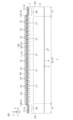
- Figure 10 is a perspective view showing the configuration of the outer peripheral region 10.
- Figure 11 is a cross-sectional view showing a main part of the outer peripheral region 10.
- the semiconductor device 1 includes a p-type well region 37 formed in a surface layer portion of the outer peripheral surface 12.
- the well region 37 is formed at a distance from the periphery of the outer peripheral surface 12 (first to fourth side surfaces 5A to 5D) toward the active surface 11 in a plan view, and extends in a band shape along the active surface 11.
- the well region 37 is formed in a ring shape (specifically, a square ring shape) surrounding the active surface 11 in a plan view.
- the well region 37 is pulled out from the surface portion of the outer peripheral surface 12 toward the first to fourth connection surfaces 13A to 13D and extends along the surface portions of the first to fourth connection surfaces 13A to 13D.
- the well region 37 is electrically connected to the body region 15 at the surface portion of the active surface 11.
- the well region 37 is formed at a distance from the lower end of the semiconductor layer 7 towards the outer circumferential surface 12, and faces the base layer 6 with a part of the semiconductor layer 7 in between.
- the well region 37 forms a pn junction with the semiconductor layer 7.
- the well region 37 may have a peak p-type impurity concentration of 1 ⁇ 10 15 cm -3 or more and 1 ⁇ 10 18 cm -3 or less.
- the well region 37 has a p-type impurity concentration lower than the p-type impurity concentration of the contact region 34.
- the p-type impurity concentration of the well region 37 may be higher than the p-type impurity concentration of the body region 15. Of course, the p-type impurity concentration of the well region 37 may be lower than the body region 15. It is preferable that the p-type impurity concentration of the well region 37 is adjusted by at least one kind of trivalent element.
- the trivalent element of the well region 37 may be the same kind as the trivalent element of the electric field relaxation structure 21, or may be a different kind from the trivalent element of the electric field relaxation structure 21.
- the trivalent element of the well region 37 may be at least one kind of boron, aluminum, gallium, and indium.
- the semiconductor device 1 includes at least one (preferably 2 to 20) p-type field region 38 formed in the surface layer of the outer peripheral surface 12 (first main surface 3) in the outer peripheral region 10.
- the number of the multiple field regions 38 is typically 4 to 8.
- the multiple field regions 38 are formed in an electrically floating state, and relieve the electric field within the chip 2 at the periphery of the first main surface 3.
- the number, width, depth, p-type impurity concentration, etc. of the field regions 38 are arbitrary and can take various values depending on the electric field to be relieved.
- the multiple field regions 38 are arranged at intervals from the periphery of the active surface 11 (first to fourth connection surfaces 13A to 13D) and the periphery of the chip 2 (first to fourth side surfaces 5A to 5D). Specifically, the multiple field regions 38 are arranged at intervals from the well region 37 to the periphery side of the outer circumferential surface 12.
- the multiple field regions 38 are formed in a band shape extending along the active region 9 in a planar view.
- the multiple field regions 38 each have a portion extending in a band shape in the first direction X and a portion extending in a band shape in the second direction Y.
- the multiple field regions 38 are formed in a ring shape (specifically, a square ring shape) surrounding the active region 9 (i.e., the multiple electric field relaxation structures 21) in a planar view.
- the multiple field regions 38 are formed in the semiconductor layer 7 at intervals from the lower end of the semiconductor layer 7 toward the outer circumferential surface 12, and form a pn junction with the semiconductor layer 7. It is preferable that the multiple field regions 38 have a bottom portion located on the outer circumferential surface 12 side relative to the intermediate portion of the thickness range of the semiconductor layer 7.
- the multiple field regions 38 are formed at intervals from the multiple electric field relaxation structures 21 toward the peripheral edge of the chip 2. Therefore, the multiple field regions 38 do not face the multiple electric field relaxation structures 21 in the vertical direction Z.
- the multiple field regions 38 are located closer to the second main surface 4 of the semiconductor layer 7 than the bottom wall of the trench structure 16.
- the bottoms of the multiple field regions 38 may be located closer to the first main surface 3 of the semiconductor layer 7 than the depth positions of the bottoms of the multiple electric field relaxation structures 21.
- the bottoms of the multiple field regions 38 may be located closer to the second main surface 4 of the semiconductor layer 7 than the depth positions of the bottoms of the multiple electric field relaxation structures 21.
- the plurality of field regions 38 may have a peak p-type impurity concentration of 1 ⁇ 10 15 cm ⁇ 3 or more and 1 ⁇ 10 18 cm ⁇ 3 or less.
- the p-type impurity concentration of the field region 38 may be approximately equal to the p-type impurity concentration of the body region 15.
- the p-type impurity concentration of the plurality of field regions 38 may be higher than the p-type impurity concentration of the body region 15.
- the p-type impurity concentration of the plurality of field regions 38 may be lower than the p-type impurity concentration of the body region 15.
- the p-type impurity concentration of the multiple field regions 38 is preferably adjusted by at least one type of trivalent element.
- the trivalent element of the field region 38 may be the same type as the trivalent element of the electric field relaxation structure 21, or may be a different type from the trivalent element of the electric field relaxation structure 21.
- the trivalent element of the field region 38 may be at least one type of boron, aluminum, gallium, and indium.
- the multiple field regions 38 are preferably formed at a pitch different from the relaxation pitch PR of the electric field relaxation structure 21. It is particularly preferable that the pitch of the multiple field regions 38 is smaller than the relaxation pitch PR. The pitch of the multiple field regions 38 may be larger than the relaxation pitch PR. The pitch of the multiple field regions 38 may be approximately equal to the relaxation pitch PR.
- the semiconductor device 1 includes an interlayer insulating film 39 covering the first main surface 3.
- the interlayer insulating film 39 may be referred to as an "insulating film,” an "interlayer film,” an “intermediate insulating film,” or the like.
- the interlayer insulating film 39 has a layered structure including a first insulating film 40 and a second insulating film 41.
- the first insulating film 40 may include at least one of a silicon oxide film, a silicon nitride film, and a silicon oxynitride film. It is particularly preferable that the first insulating film 40 includes a silicon oxide film made of an oxide of the chip 2 (semiconductor layer 7).
- the first insulating film 40 selectively covers the first main surface 3 in the active region 9 and the peripheral region 10. Specifically, the first insulating film 40 selectively covers the active surface 11, the peripheral surface 12, and the first to fourth connection surfaces 13A to 13D. The first insulating film 40 is connected to the insulating film 18 in the active surface 11, exposing the buried electrode 19.
- the first insulating film 40 covers the well region 37 and the multiple field regions 38 on the outer peripheral surface 12.
- the first insulating film 40 is continuous with the first to fourth side surfaces 5A to 5D.
- the first insulating film 40 may be formed at a distance inward from the periphery of the outer peripheral surface 12, exposing the semiconductor layer 7 from the periphery of the outer peripheral surface 12.
- the first insulating film 40 covers the body region 15 and well region 37 on the first to fourth connection surfaces 13A to 13D.
- the second insulating film 41 is laminated on the first insulating film 40.
- the second insulating film 41 may include at least one of a silicon oxide film, a silicon nitride film, and a silicon oxynitride film.
- the interlayer insulating film 39 preferably includes a silicon oxide film.
- the second insulating film 41 covers the first main surface 3 in the active region 9 and the peripheral region 10, sandwiching the first insulating film 40 between them. Specifically, the second insulating film 41 selectively covers the active surface 11, the peripheral surface 12, and the first to fourth connection surfaces 13A to 13D, sandwiching the first insulating film 40 between them.
- the second insulating film 41 covers the multiple trench structures 16 (buried electrodes 19) in the active region 9.
- the second insulating film 41 covers the well region 37 and multiple field regions 38 in the peripheral region 10, sandwiching the first insulating film 40 between them.
- the second insulating film 41 is continuous with the first to fourth side surfaces 5A to 5D.
- the second insulating film 41 may be formed at a distance inward from the periphery of the peripheral surface 12, exposing the periphery of the first main surface 3 together with the first insulating film 40.
- the semiconductor device 1 includes a plurality of contact openings 42 formed in the interlayer insulating film 39.
- the plurality of contact openings 42 include a plurality of contact openings 42 (not shown) that expose a plurality of trench structures 16 (buried electrodes 19), and a plurality of contact openings 42 that expose a plurality of source regions 33.
- the plurality of contact openings 42 for the source regions 33 are formed in the regions between the plurality of adjacent trench structures 16, and expose the plurality of source regions 33 and the plurality of contact regions 34.
- the semiconductor device 1 includes a sidewall structure 43 disposed in the interlayer insulating film 39 so as to cover at least one of the first to fourth connection surfaces 13A to 13D.
- the sidewall structure 43 is disposed on the first insulating film 40 and is covered by the second insulating film 41.
- the sidewall structure 43 reduces the step formed between the active surface 11 and the outer peripheral surface 12.
- the sidewall structure 43 is formed in a band shape extending along at least one of the first to fourth connection surfaces 13A to 13D.
- the sidewall structure 43 is formed in a ring shape (specifically, a square ring shape) extending along the first to fourth connection surfaces 13A to 13D so as to surround the active surface 11 in a plan view.
- the sidewall structure 43 may have a portion that extends in a film shape along the outer peripheral surface 12, and a portion that extends in a film shape along the first to fourth connection surfaces 13A to 13D.
- the sidewall structure 43 is formed at a distance from the innermost field region 38 toward the active surface 11, and faces the well region 37 in the horizontal and vertical directions Z, sandwiching the first insulating film 40 therebetween.
- the sidewall structure 43 may face the body region 15, sandwiching the first insulating film 40 therebetween.
- the semiconductor device 1 includes a gate pad 44 disposed on the interlayer insulating film 39.
- the gate pad 44 is an electrode to which a gate potential is applied from the outside.
- the gate pad 44 may be referred to as a "gate pad electrode", a "first pad electrode”, etc.
- the gate pad 44 may have a layered structure including a Ti-based metal film and an Al-based metal film layered in this order from the interlayer insulating film 39 side.
- the gate pad 44 is disposed on a portion of the interlayer insulating film 39 that covers the active region 9. Specifically, the gate pad 44 is disposed on the active surface 11 at a distance from the outer peripheral surface 12 in a plan view. The gate pad 44 is disposed in a region close to the center of one side of the active surface 11 (the second connection surface 13B in this embodiment) in a plan view.
- the gate pad 44 may be disposed in a region along any of the central portions of the first to fourth connection surfaces 13A to 13D.
- the gate pad 44 may be disposed at any corner of the active surface 11 in a planar view.
- the gate pad 44 may also be disposed at the central portion of the active surface 11 in a planar view.
- the gate pad 44 is formed in a quadrangular shape in a planar view.
- the semiconductor device 1 includes at least one gate wiring 45 (multiple in this embodiment) that is drawn from the gate pad 44 onto the interlayer insulating film 39.
- the gate wiring 45 may also be referred to as a "wiring", a “wiring electrode”, etc.
- the multiple gate wirings 45 are arranged on the active surface 11 at a distance from the outer peripheral surface 12 in a plan view.
- the multiple gate wirings 45 may have a laminated structure including a Ti-based metal film and an Al-based metal film laminated in this order from the interlayer insulating film 39 side.
- the multiple gate wirings 45 include a first gate wiring 45A and a second gate wiring 45B.
- the first gate wiring 45A is pulled out from the gate pad 44 toward the first connection surface 13A and extends in a line along the periphery of the active surface 11 so as to intersect (specifically, perpendicularly) with a portion (specifically, one end) of the multiple trench structures 16.
- the first gate wiring 45A penetrates the interlayer insulating film 39 via the multiple contact openings 42 and is electrically connected to one end of the multiple trench structures 16.
- the second gate wiring 45B is pulled out from the gate pad 44 toward the third connection surface 13C and extends in a line along the periphery of the active surface 11 so as to intersect (specifically, perpendicular to) a portion (specifically, the other end) of the multiple trench structures 16.
- the second gate wiring 45B penetrates the interlayer insulating film 39 via the multiple contact openings 42 and is electrically connected to the other end of the multiple trench structures 16.
- the semiconductor device 1 includes a source pad 46 disposed on the interlayer insulating film 39 at a distance from the gate pad 44 and the gate wiring 45.
- the source pad 46 is an electrode to which a source potential is applied from the outside.
- the source pad 46 may be referred to as a "source pad electrode", a "second pad electrode”, etc.
- the source pad 46 may have a layered structure including a Ti-based metal film and an Al-based metal film layered in this order from the interlayer insulating film 39 side.
- the source pad 46 is disposed on the active surface 11 at a distance from the outer peripheral surface 12 in a plan view.
- the source pad 46 is formed in a polygonal shape having a recess along the gate pad 44 in a plan view.
- the source pad 46 may also be formed in a square shape in a plan view.
- the source pad 46 penetrates the interlayer insulating film 39 through a plurality of contact openings 42, and is electrically connected to the body region 15, the plurality of source regions 33, and the plurality of contact regions 34. In other words, the source pad 46 is electrically connected to the plurality of electric field relaxation structures 21 through the body region 15.
- the semiconductor device 1 includes a drain pad 47 covering the second main surface 4.
- the drain pad 47 is an electrode to which a drain potential is applied from the outside.
- the drain pad 47 may be referred to as a "drain pad electrode”, a “third pad electrode”, etc.
- the drain pad 47 forms an ohmic contact with the base layer 6 exposed from the second main surface 4.
- the drain pad 47 is electrically connected to the multiple drift regions 8 via the base layer 6.
- the drain pad 47 may cover the entire second main surface 4 so as to be continuous with the periphery of the chip 2 (first to fourth side surfaces 5A to 5D).
- the drain pad 47 may cover the second main surface 4 at a distance inward from the periphery of the chip 2 so as to expose the periphery of the chip 2.
- the breakdown voltage that can be applied between the source pad 46 and the drain pad 47 (between the first main surface 3 and the second main surface 4) may be 500 V or more and 3000 V or less.
- the breakdown voltage may have a value that belongs to any one of the following ranges: 500 V or more and 1000 V or less, 1000 V or more and 1500 V or less, 1500 V or more and 2000 V or less, 2000 V or more and 2500 V or less, and 2500 V or more and 3000 V or less.
- FIG. 12 is a schematic diagram showing a wafer 50 used in the manufacture of the semiconductor device 1.
- the wafer 50 is a substrate for the base layer 6 and contains SiC single crystal.
- the wafer 50 is formed in a flat disk shape. Of course, the wafer 50 may also be formed in a flat rectangular parallelepiped shape.
- the wafer 50 has a first wafer main surface 51 on one side, a second wafer main surface 52 on the other side, and a wafer side surface 53 connecting the first wafer main surface 51 and the second wafer main surface 52.
- the first wafer main surface 51 corresponds to the upper end of the base layer 6, and the second wafer main surface 52 corresponds to the lower end of the base layer 6.
- the first wafer main surface 51 and the second wafer main surface 52 are formed by the c-plane of the SiC single crystal.
- the first wafer main surface 51 is formed by the silicon surface of the SiC single crystal, and the second wafer main surface 52 is formed by the carbon surface of the SiC single crystal.
- the wafer 50 (the first wafer main surface 51 and the second wafer main surface 52) has the off-direction Do and off-angle ⁇ o described above.
- the wafer 50 has a mark 54 on the wafer side surface 53 that indicates the crystal orientation of the SiC single crystal.
- the mark 54 may include either or both of an orientation flat and an orientation notch.
- the orientation flat consists of a cutout that is cut in a straight line in a plan view.
- the orientation notch consists of a cutout that is cut in a concave shape (e.g., a tapered shape) toward the center of the first wafer main surface 51 in a plan view.
- the mark 54 may include either or both of a first orientation flat extending in the m-axis direction and a second orientation flat extending in the a-axis direction.
- the mark 54 may include either or both of an orientation notch recessed in the m-axis direction and an orientation notch recessed in the a-axis direction.
- FIG. 12 an orientation flat extending in the m-axis direction (first direction X) in a plan view is shown.
- a plurality of device regions 55 and a plurality of cutting lines 56 are set on the wafer 50 by alignment marks or the like.
- Each device region 55 is an area corresponding to a semiconductor device 1.
- Each of the plurality of device regions 55 is set to have a rectangular shape in a plan view.
- the multiple device regions 55 are set in a matrix along the first direction X and the second direction Y in a plan view.
- the multiple device regions 55 are each set at intervals inward from the periphery of the first wafer main surface 51 in a plan view.
- the multiple cutting lines 56 are set in a lattice extending along the first direction X and the second direction Y to partition the multiple device regions 55.
- FIG. 13 is a flowchart showing an example of a method for manufacturing the semiconductor device 1.
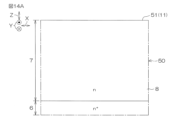
- FIG. 14A to FIG. 14H are cross-sectional views showing an example of a method for manufacturing the semiconductor device 1.
- FIG. 14A to FIG. 14H are cross-sectional views corresponding to FIG. 7.
- the aforementioned wafer 50 preparation process is carried out (step S1 in FIG. 13).
- the semiconductor layer 7 formation process is carried out (step S2 in FIG. 13).
- the semiconductor layer 7 is formed starting from the first wafer main surface 51 (wafer 50) by epitaxial growth.
- step S3 in FIG. 13 the process of forming the body region 15 is carried out.
- p-type impurities are introduced into the entire semiconductor layer 7.
- the body region 15 is formed over the entire surface portion of the semiconductor layer 7.
- a step of forming a first mask 60 having a predetermined pattern is performed (step S4 in FIG. 13).
- the first mask 60 is preferably an inorganic mask (hard mask).
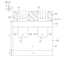
- the first mask 60 is disposed on the upper end of the semiconductor layer 7, and has a plurality of first openings 61 that expose regions in which a plurality of electric field relaxation structures 21 are to be formed.
- a step of forming a plurality of electric field relaxation structures 21 is performed (step S5 in FIG. 13).
- p-type impurities are selectively introduced into the semiconductor layer 7 via the first mask 60. This forms the electric field relaxation structures 21 connected to the lower portion of the body region 15.
- the electric field relaxation structure 21 may be formed by a channeling ion implantation method.
- the channeling implantation process is performed based on data (information) of the off angle ⁇ o. If it is a channeling implantation process, the electric field relaxation structure 21 can be selectively and easily formed at a deep position in the semiconductor layer 7. If the electric field relaxation structure 21 is formed by a channeling ion implantation method, the electric field relaxation structure 21 may be formed before the body region 15.
- the first mask 60 is removed (step S6 in FIG. 13).
- a process for forming a plurality of source regions 33 is carried out (step S7 in FIG. 13).
- the plurality of source regions 33 are formed by introducing n-type impurities into the surface layer of the semiconductor layer 7 by ion implantation through a mask (not shown) having a predetermined layout.
- a process for forming a plurality of contact regions 34 is performed (step S8 in FIG. 13).
- the plurality of contact regions 34 are formed by introducing p-type impurities into the surface layer of the semiconductor layer 7 by ion implantation through a mask (not shown) having a predetermined layout.
- the first contact region 35 and the second contact region 36 are formed physically independent of each other.
- the process for forming the contact regions 34 may be performed prior to the process for forming the source region 33.
- a process for forming a plurality of trenches 17 is performed.
- a second mask (not shown) having a predetermined pattern is formed (step S9 in FIG. 13).
- the second mask is preferably an inorganic mask (hard mask).
- unnecessary portions of the semiconductor layer 7 are removed by an etching method via the second mask.
- the etching method may be either or both of a wet etching method and a dry etching method.
- the etching method is preferably an RIE (Reactive Ion Etching) method.
- RIE Reactive Ion Etching
- a step of forming the insulating film 18 is performed (step S11 in FIG. 13).
- the step of forming the insulating film 18 also serves as a step of forming the first insulating film 40.
- the insulating film 18 may be formed by either one or both of a CVD (Chemical Vapor Deposition) method and an oxidation process method.
- the insulating film 18 and the first insulating film 40 are typically formed by a thermal oxidation process method.
- the insulating film 18 is formed in the form of a film on the wall surfaces of the multiple trenches 17, and the first insulating film 40 is formed in the form of a film in the region of the upper end of the semiconductor layer 7 outside the multiple trenches 17.
- a process for forming the buried electrode 19 is performed (step S12 in FIG. 13).
- This process includes a process for forming a base electrode film on the insulating film 18.
- the base electrode film includes conductive polysilicon.
- the base electrode film backfills the multiple trenches 17 and covers the upper end of the semiconductor layer 7.
- the base electrode film may be formed by a CVD method.
- unnecessary portions of the buried electrode 19 are removed by an etching method.
- the unnecessary portions of the buried electrode 19 are removed until the insulating film 18 is exposed.
- the etching method may be either one or both of a wet etching method and a dry etching method. As a result, multiple buried electrodes 19 are buried in the multiple trenches 17, respectively, and multiple trench structures 16 are formed.
- the interlayer insulating film 39 may be formed by a CVD method.
- a plurality of contact openings 42 having a predetermined layout are formed in the interlayer insulating film 39 by an etching method using a mask (not shown) having a predetermined layout.
- the gate pad 44, gate wiring 45, and source pad 46 are formed by depositing a metal film on the interlayer insulating film 39 by sputtering, and then shaping it into a predetermined layout by etching using a mask (not shown) having a predetermined layout.
- drain pad 47 is formed by depositing a metal film on the second wafer main surface 52 by a sputtering method.
- the wafer 50 is then cut along a number of intended cutting lines 56 (step S16 in FIG. 13).
- the electric field relaxation structure 21 is formed on the bottom wall of the trench 17, so that the electric field concentration on the bottom wall of the trench 17 in the trench gate structure related to the MISFET (Metal Insulator Semiconductor Field Effect Transistor) can be mitigated.
- MISFET Metal Insulator Semiconductor Field Effect Transistor
- the electric field relaxation structure 21 is not formed one-to-one with each trench 17, but spans the bottom walls of multiple trenches 17. In this form, one electric field relaxation structure 21 spans the bottom walls of two adjacent trenches 17. This allows the dimensions of the electric field relaxation structure 21 (e.g., relaxation width WR, relaxation pitch PR, etc.) to be set with an independent design that is not dependent on the width WT of each trench 17 or the pitch PT of multiple trenches 17. As a result, with appropriate design, the electric field relaxation structure 21 can be easily fabricated.
- the electric field relaxation structure 21 e.g., relaxation width WR, relaxation pitch PR, etc.
- a sufficient processing dimension margin can be obtained by using a pattern of the electric field relaxation structure 21 having a width WR wider than the trench pitch PT.
- the trench pitch PT the relaxation pitch PR
- the electric field relaxation structure 21 will be formed horizontally away from the trench 17, and the bottom wall of the trench 17 will not be covered with the electric field relaxation structure 21, which may cause a decrease in breakdown voltage.
- the electric field relaxation structure 21 is formed wide in the horizontal direction, so that the bottom wall of the trench 17 can be reliably covered with the electric field relaxation structure 21.
- the electric field relaxation structure 21 must be formed deeper than the body region 15, so the first mask 60 must be formed relatively thick.
- the ions In order to implant ions deep into the region, the ions must be accelerated with high energy, and this is to prevent the accelerated ions from penetrating the first mask 60 for implantation. Therefore, as the width of the first mask 60 becomes narrower due to miniaturization, the aspect ratio of the first mask 60 tends to become higher. If the aspect ratio is high, the durability of the first mask 60 against external forces decreases, and the first mask 60 is more likely to fall or tilt due to its own weight or external forces.
- the dimensions of the electric field relaxation structure 21 can be designed independently of the dimensions of the trench 17, the aspect ratio of the first mask 60 can be kept low. As a result, the electric field relaxation structure 21 can be formed with high precision even if the trench 17 is miniaturized.
- the portion of the body region 15 that is physically and electrically integrated with the electric field relaxation structure 21 is covered with the second conductivity type portion (body region 15 and electric field relaxation structure 21) from the sidewall to the bottom wall of the trench 17. Since the range in which an inversion layer should be formed along the inner wall of the trench 17 is long, the voltage (threshold voltage) required to form a channel tends to be selectively higher than that of the channel portion 22. Therefore, by making the portion of the body region 15 that is physically and electrically integrated with the electric field relaxation structure 21 into a non-channel portion 23, it is possible to suppress variation in the threshold voltage of the semiconductor device 1.
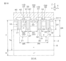
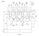
- FIGS. 15 to 20 are diagrams showing first to sixth modified examples of the semiconductor device 1. Next, the modified examples of the semiconductor device 1 will be described with reference to FIGS. 15 to 20.
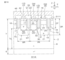
- each electric field relaxation structure 21 may have an end 30 at the position of the wall surface (sidewall) of the trench 17 on the channel portion 22 side in the width direction of the trench 17.
- the wall surface (sidewall) of the trench 17 and the end 30 of the electric field relaxation structure 21 may be linearly continuous in the vertical direction Z.
- the bottom wall of the trench 17 is completely covered by the electric field relaxation structure 21, so the electric field concentration on the bottom wall of the trench 17 can be further alleviated.
- the electric field relaxation structure 21 acts as an obstacle, making it difficult for a current path to form in the portion of the bottom wall of the trench 17 on the channel portion 22 side. Therefore, compared to Figures 7 to 9, there is a possibility that the on-resistance may increase. In other words, the structures of Figures 7 to 9 can achieve a good balance between alleviating the electric field concentration on the bottom wall of the trench 17 and reducing the on-resistance.
- each electric field relaxation structure 21 may be a curved surface that bulges out toward the channel portion 22 in the horizontal direction (at least one of the first direction X and the second direction Y) instead of being a flat surface that is parallel or approximately parallel to the vertical direction Z from the bottom wall of the trench 17.
- the curved apex 70 of the end 30 of each electric field relaxation structure 21 is located inside (on the non-channel section 23 side) relative to the wall surface (sidewall) of the trench 17 on the channel section 22 side.
- the curved end 30 is formed to be set back toward the non-channel section 23 side in the horizontal direction relative to the wall surface (sidewall) of the trench 17 on the channel section 22 side.
- a source region 33 may be formed in a portion of the non-channel portion 23.
- a plurality of source regions 33 may be formed at intervals in the extension direction of the corresponding trench structure 16 in a plan view.
- the non-channel portion 23 has an electric field relaxation structure 21 with a higher p-type impurity concentration than the body region 15, so a channel (inversion layer) is less likely to form in the non-channel portion 23 than in the channel portion 22. Despite these conditions, by forming a source region 33 in the non-channel portion 23, the non-channel portion 23 can also be given the function of channel formation.
- the first width W1 of the mesa portion 20 that forms the channel portion 22 may be wider than the second width W2 of the mesa portion 20 that forms the non-channel portion 23.
- the ratio of the channel portion 22 to the entire chip 2 can be increased, thereby improving the channel density.
- the multiple electric field relaxation structures 21 may span the bottom walls of three or more trenches 17 that are continuous in the first direction X. In this case, each electric field relaxation structure 21 spans the bottom walls of both end trenches 17 of the three or more trenches 17 that are continuous in the first direction X. In FIG. 19, each electric field relaxation structure 21 spans the bottom walls of three trenches 17 that are continuous in the first direction X.
- the bottom wall of the central trench 17 of the three trenches 17 is completely covered by the electric field relaxation structure 21.
- the body regions 15 on both sides of the central trench 17 in the first direction X are non-channel portions 23 connected to the electric field relaxation structure 21.
- the bottom walls of the two trenches 17 at both ends of the three trenches 17 are partially covered by the electric field relaxation structure 21.
- the bottom walls of the two trenches 17 at both ends have a first portion 31 covered by the electric field relaxation structure 21 and a second portion 32 covered by the semiconductor layer 7 (drift region 8).
- the element structure of the semiconductor device 1 may be an IGBT (Insulated Gate Bipolar Transistor) structure, unlike the MISFET structure of FIGS. 7 to 9.
- a p-type collector region 71 may be formed instead of the base layer 6.
- a p-type base region 72 may be formed by the body region 15, and an n-type emitter region 73 may be formed by the source region 33.
- the electric field relaxation structure 21 spans the bottom walls of multiple trenches 17. This makes it possible to relax the electric field concentration on the bottom walls of the trenches 17 in the trench gate structure of the IGBT.
- the base layer 6 and the semiconductor layer 7 each contain a SiC single crystal.
- at least one or all of the base layer 6 and the semiconductor layer 7 may contain a single crystal of a wide band gap semiconductor other than a SiC single crystal.
- a wide band gap semiconductor is a semiconductor having a band gap larger than that of silicon.
- Examples of single crystals of wide band gap semiconductors include silicon carbide (SiC), gallium nitride (GaN), diamond (C), and gallium oxide (Ga 2 O 3 ).
- the base layer 6 and the semiconductor layer 7 may be made of the same type of single crystal, or may be made of different types of single crystal. At least one or all of the base layer 6 and the semiconductor layer 7 may be made of silicon (Si).
- semiconductor device in the following items may be replaced with "SiC semiconductor device,” “wide band gap semiconductor device,” “semiconductor switching device,” “semiconductor rectifier device,” “MISFET device,” “IGBT device,” “diode device,” etc., as necessary.
- a chip (2) having a first major surface (3) and an opposite second major surface (4); a first impurity region (7, 8) of a first conductivity type formed in a surface layer portion of the first main surface (3); a second impurity region (15, 72) of a second conductivity type formed in a surface layer portion of the first impurity region (7, 8); a third impurity region (33, 73) of the first conductivity type formed in a surface layer portion of the second impurity region (15, 72); a plurality of trenches (17) extending from the first main surface (3) through the third impurity region (33, 73) and the second impurity region (15, 72) to reach the first impurity region (7, 8); and a second conductivity type electric field relaxation structure (21) formed integrally with the second impurity region (15, 72) and spanning the bottom walls of the plurality of trenches (17).
- the electric field relaxation structure (21) is formed on the bottom wall of the trench (17), it is possible to relax the electric field concentration on the bottom wall of the trench (17).
- the electric field relaxation structure (21) is not formed one-to-one with each trench (17), but spans the bottom walls of multiple trenches (17). This allows the dimensions of the electric field relaxation structure (21) to be set by an independent design that does not depend on the width of each trench (17) or the pitch of the multiple trenches (17). As a result, the electric field relaxation structure (21) can be easily manufactured by appropriate design. For example, even under design conditions where the pitch of the multiple trench (17) patterns is narrow due to miniaturization, a sufficient processing dimension margin can be obtained by using a pattern of the electric field relaxation structure (21) having a width wider than the pitch of the trenches (17).
- Appendix 1-2 The semiconductor device (1) described in Appendix 1-1, wherein the second impurity region (15, 72) includes a channel portion (22) that is physically and electrically separated from the electric field relaxation structure (21), in which a channel is formed along the trench (17) adjacent to the channel portion (22), and a non-channel portion (23) that is physically and electrically integrated with the electric field relaxation structure (21) and has a bottom wall covered by the electric field relaxation structure (21).
- the portion of the second impurity region (15, 72) that is physically and electrically integrated with the electric field relaxation structure (21) is covered with the second conductivity type portion (the second impurity region (15, 72) and the electric field relaxation structure (21)) from the sidewall to the bottom wall of the trench (17). Since the range in which an inversion layer should be formed along the inner wall of the trench (17) is long, the voltage required for channel formation (threshold voltage) tends to be selectively high in that portion. Therefore, by making the portion of the second impurity region (15, 72) that is physically and electrically integrated with the electric field relaxation structure (21) into a non-channel portion (23), it is possible to suppress the variation in the threshold voltage.
- the width (W1) of the channel portion (22) can be made wider than the non-channel portion (23), thereby increasing the ratio of the channel portion (22) to the entire chip (2), thereby improving the channel density.
- Appendix 1-4 The semiconductor device (1) described in Appendix 1-2 or Appendix 1-3, wherein the electric field relaxation structure (21) has an end portion (30) at a central position of the bottom wall on the non-channel portion (23) side relative to a wall surface of the trench (17) on the channel portion (22) side in the width direction of the trench (17).
- the portion of the bottom wall of the trench (17) on the channel portion (22) side is covered with the first impurity region (7, 8) (first conductivity type), so that a sufficient current path can be secured along the wall surface of the trench (17) on the channel portion (22) side. This makes it possible to reduce the on-resistance.
- the third impurity region (33, 73) is selectively formed in the channel portion (22) of the channel portion (22) and the non-channel portion (23); a fourth impurity region (34, 35, 36) of a second conductivity type formed in a surface layer portion of the second impurity region (15, 72) and having a higher impurity concentration than the second impurity region (15, 72);
- the semiconductor device (1) according to any one of Supplementary Notes 1-2 to 1-5, wherein the fourth impurity region (34, 35, 36) includes a first contact region (35) formed in the non-channel portion (23).
- the third impurity region (33, 73) is selectively formed in the channel portion (22) of the channel portion (22) and the non-channel portion (23).
- the third impurity region (33, 73) is not formed in the non-channel portion (23), and the first contact region (35) is formed.
- This configuration ensures electrical contact with the second impurity region (15, 72) even in the channel portion (22).
- the channel portion (22) and the non-channel portion (23) are each partitioned into regions sandwiched between a plurality of the trenches (17),
- the first contact region (35) is formed over the entire first main surface (3) between the trench (17) on one side of the non-channel portion (23) and the trench (17) on the other side of the non-channel portion (23);
- a channel in the channel portion (22), a channel can be formed on the wall surfaces of both the trench (17) on one side and the trench (17) on the other side. Since multiple current paths can be formed in one channel portion (22), the on-resistance can be reduced.
- a plurality of the electric field relaxation structures (21) are arranged at intervals, The semiconductor device (1) according to any one of Appendix 1-1 to Appendix 1-8, wherein the pitch (PR) between adjacent electric field relaxation structures (21) is at least twice the pitch (PT) between adjacent trenches (17).
- the depth (DT) of the trench (17) is 0.5 ⁇ m or more and 1.5 ⁇ m or less,
- the semiconductor device (1) according to any one of Appendix 1-1 to Appendix 1-12, wherein the depth (DR) of the electric field relaxation structure (21) is 2 ⁇ m or more and 3 ⁇ m or less.
- Appendix 1-16 a drain region (6) of a first conductivity type formed on the second main surface (4) side with respect to the first impurity region (7, 8); a body region (15) formed by the second impurity region (15, 72); a source region (33) formed by the third impurity region (33, 73);
- the semiconductor device (1) according to any one of Appendices 1-1 to 1-15, comprising a trench gate structure (16) formed by the trench (17), an insulating film (18) covering a wall surface of the trench (17), and a buried electrode (19) buried in the trench (17).
- This configuration makes it possible to easily manufacture a structure that can reduce electric field concentration on the bottom wall of a trench gate structure (16) related to a MISFET (Metal Insulator Semiconductor Field Effect Transistor).
- MISFET Metal Insulator Semiconductor Field Effect Transistor
- Appendix 1-17 a collector region (71) of a second conductivity type formed on the second main surface (4) side with respect to the first impurity region (7, 8); a base region (72) formed by the second impurity region (15, 72); an emitter region (73) formed by the third impurity region (33, 73);
- the semiconductor device (1) according to any one of Appendices 1-1 to 1-15, comprising a trench gate structure (16) formed by the trench (17), an insulating film (18) covering a wall surface of the trench (17), and a buried electrode (19) buried in the trench (17).
- This configuration makes it easy to manufacture a structure that can reduce electric field concentration on the bottom wall of a trench gate structure (16) for an IGBT (Insulated Gate Bipolar Transistor).
- IGBT Insulated Gate Bipolar Transistor
- the impurity concentration of the second impurity region (15, 72) is 1 ⁇ 10 15 cm ⁇ 3 or more and 1 ⁇ 10 18 cm ⁇ 3 or less,
Landscapes
- Electrodes Of Semiconductors (AREA)
Abstract
半導体装置は、第1主面およびその反対側の第2主面を有するチップと、前記第1主面の表層部に形成された第1導電型の第1不純物領域と、前記第1不純物領域の表層部に形成された第2導電型の第2不純物領域と、前記第2不純物領域の表層部に形成された第1導電型の第3不純物領域と、前記第1主面から前記第3不純物領域および前記第2不純物領域を通って前記第1不純物領域に達する複数のトレンチと、前記第2不純物領域と一体的に形成され、前記複数のトレンチの底壁に跨る第2導電型の電界緩和構造とを含む。
Description
本出願は、2023年6月26日に日本国特許庁に提出された特願2023-104405号に対応しており、この出願の全開示はここに引用により組み込まれるものとする。
本開示は、半導体装置に関する。
特許文献1は、チャネリング注入法によって炭化ケイ素層に導入された不純物領域を有する電子デバイスを開示している。
[概要]
本開示の一実施形態は、トレンチ底壁への電界集中を緩和できる構造を容易に製造可能な半導体装置を提供する。
本開示の一実施形態は、トレンチ底壁への電界集中を緩和できる構造を容易に製造可能な半導体装置を提供する。
本開示の一実施形態に係る半導体装置は、第1主面およびその反対側の第2主面を有するチップと、前記第1主面の表層部に形成された第1導電型の第1不純物領域と、前記第1不純物領域の表層部に形成された第2導電型の第2不純物領域と、前記第2不純物領域の表層部に形成された第1導電型の第3不純物領域と、前記第1主面から前記第3不純物領域および前記第2不純物領域を通って前記第1不純物領域に達する複数のトレンチと、前記第2不純物領域と一体的に形成され、前記複数のトレンチの底壁に跨る第2導電型の電界緩和構造とを含む。
[詳細な説明]
次に、本開示の実施形態を、添付図面を参照して詳細に説明する。
次に、本開示の実施形態を、添付図面を参照して詳細に説明する。
添付図面は、いずれも模式図であり、厳密に図示されたものではなく、縮尺、比率、角度等は必ずしも一致しない。添付図面の間で対応する構造には同一の参照符号が付され、重複する説明は省略または簡略化される。説明が省略または簡略化された構造については、省略または簡略化される前になされた説明が適用される。
この明細書において「ほぼ(substantially)」の文言が使用される場合、この文言は、比較対象の数値(形態)と等しい数値(形態)を含む他、比較対象の数値(形態)を基準とする±10%の範囲の数値誤差(形態誤差)も含む。以下の説明では「第1」、「第2」、「第3」等の文言が使用されるが、これらは説明順序を明確にするために各構造の名称に付された記号であり、各構造の名称を限定する趣旨で付されていない。
以下の説明では、「p型」または「n型」を用いて半導体(不純物)の導電型が示されるが、「p型」が「第1導電型」と称され、「n型」が「第2導電型」と称されてもよい。むろん、「n型」が「第1導電型」と称され、「p型」が「第2導電型」と称されてもよい。「p型」は3価元素に起因する導電型であり、「n型」は5価元素に起因する導電型である。3価元素は、特に言及されない限り、ホウ素、アルミニウム、ガリウムおよびインジウムのうちの少なくとも1種である。5価元素は、特に言及されない限り、窒素、リン、ヒ素、アンチモンおよびビスマスのうちの少なくとも1種である。
図1は、実施形態に係る半導体装置1を示す平面図である。図2は、図1に示すII-II線に沿う断面図である。図3は、チップ2のレイアウト例を示す平面図である。図4は、チップ2のレイアウト例を示す斜視図である。図5は、活性領域9と共にトレンチ構造16を示す平面図である。図6は、活性領域9と共に、トレンチ構造16および電界緩和構造21を示す断面斜視図である。図7~図9は、トレンチ構造16および電界緩和構造21を示す拡大断面図である。図7~図9は、表示された参照符号のみが異なる同じ断面図である。電界緩和構造21の形状は、図7~図9を参照して、様々な局面から説明される。
図1~図9を参照して、半導体装置1は、SiC単結晶を含むチップ2を含む。チップ2は、「SiCチップ」または「半導体チップ」と称されてもよい。チップ2は、この形態(this embodiment)では、六方晶のSiC単結晶からなり、直方体形状に形成されている。六方晶のSiC単結晶は、2H(Hexagonal)-SiC単結晶、4H-SiC単結晶、6H-SiC単結晶等を含む複数種のポリタイプを有している。この形態では、チップ2が4H-SiC単結晶からなる例が示されるが、チップ2は他のポリタイプからなっていてもよい。
チップ2は、一方側の第1主面3、他方側の第2主面4、ならびに、第1主面3および第2主面4を接続する第1~第4側面5A~5Dを有している。第1主面3および第2主面4は、鉛直方向Zから見た平面視(以下、単に「平面視」という。)において四角形状に形成されている。鉛直方向Zは、チップ2の厚さ方向や第1主面3(第2主面4)の法線方向でもある。第1主面3および第2主面4は、平面視において正方形状または長方形状に形成されていてもよい。
第1主面3および第2主面4は、SiC単結晶のc面によって形成されていることが好ましい。この場合、第1主面3はSiC単結晶のシリコン面((0001)面)によって形成され、第2主面4はSiC単結晶のカーボン面((000-1)面)によって形成されていることが好ましい。
第1側面5Aを起点とするチップ2の周方向(図1では反時計回り)に関して、第2側面5Bは第1側面5Aに接続され、第3側面5Cは第2側面5Bに接続され、第4側面5Dは第1側面5Aおよび第3側面5Cに接続されている。第1側面5Aおよび第3側面5Cは、第1主面3に沿う第1方向Xに延び、第1方向Xに交差(具体的には直交)する第2方向Yに対向している。第2側面5Bおよび第4側面5Dは、第2方向Yに延び、第1方向Xに対向している。
この形態では、第1方向XがSiC単結晶のm軸方向([1-100]方向)であり、第2方向YがSiC単結晶のa軸方向([11-20]方向)である。むろん、第1方向XがSiC単結晶のa軸方向であり、第2方向YがSiC単結晶のm軸方向であってもよい。
第1方向Xおよび第2方向Yを含むXY平面は、鉛直方向Zに直交する水平面を形成する。以下では、鉛直方向Zに沿って延びる軸が「鉛直軸」と表現されることがある。また、以下では、第1方向Xおよび第2方向Yが「水平方向」と表現されることがある。水平方向は、第1主面3に沿って延びる方向でもある。
図4を参照して、チップ2(第1主面3および第2主面4)は、SiC単結晶のc面に対して所定のオフ方向Doに所定の角度で傾斜したオフ角θoを有している。つまり、SiC単結晶のc軸((0001)軸)は、鉛直軸からオフ方向Doに向けてオフ角θo分だけ傾斜している。また、SiC単結晶のc面は、水平面に対してオフ角θo分だけ傾斜している。
オフ方向Doは、SiC単結晶のa軸方向(つまり第2方向Y)であることが好ましい。オフ角θoは、0°を超えて10°以下であってもよい。オフ角θoは、0°を超えて1°以下、1°以上2.5°以下、2.5°以上5°以下、5°以上7.5°以下、および、7.5°以上10°以下のいずれか1つの範囲に属する値を有していてもよい。
オフ角θoは、5°以下であることが好ましい。オフ角θoは、2°以上4.5°以下であることが特に好ましい。オフ角θoは、典型的には、4°±0.1°の範囲に設定される。むろん、この明細書は、オフ角θoが0°である形態(つまり、第1主面3がc面に対してジャスト面である形態)を除外しない。
チップ2は、SiC単結晶からなるn型のベース層6を含む。ベース層6は、「ドレイン領域」、「ベースSiC層」、「ベース領域」等と称されてもよい。ベース層6は、水平方向に層状に延び、第2主面4および第1~第4側面5A~5Dの一部を形成している。ベース層6は、この形態では、SiC単結晶製の基板(つまりSiC基板)からなる。ベース層6は、前述のオフ方向Doおよびオフ角θoを有している。
ベース層6は、1×1018cm-3以上1×1021cm-3以下のn型不純物濃度をピーク値として有していてもよい。ベース層6は、厚さ方向にほぼ一定のn型不純物濃度を有していることが好ましい。ベース層6のn型不純物濃度は、単一種の5価元素によって調整されていることが好ましい。ベース層6のn型不純物濃度は、リン以外の5価元素によって調整されていることが特に好ましい。ベース層6のn型不純物濃度は、この形態では、窒素によって調整されている。
ベース層6は、第1厚さT1を有している。第1厚さT1は、5μm以上300μm以下であってもよい。第1厚さT1は、5μm以上50μm以下、50μm以上100μm以下、100μm以上150μm以下、150μm以上200μm以下、200μm以上250μm以下、および、250μm以上300μm以下のいずれか1つの範囲に属する値を有していてもよい。第1厚さT1は、50μm以上250μm以下であることが好ましい。
チップ2は、ベース層6の上に積層されたSiC単結晶製の半導体層7を含む。第1不純物領域の一例としての半導体層7は「ドリフト領域」、「SiC層」、「半導体領域」等と称されてもよい。半導体層7は、水平方向に層状に延び、第1主面3および第1~第4側面5A~5Dの一部を形成している。半導体層7は、ベース層6を起点に結晶成長されたエピタキシャル層(つまりSiCエピタキシャル層)からなる。
半導体層7は、下端および上端を有している。半導体層7の下端は結晶成長起点であり、半導体層7の上端は結晶成長終点である。半導体層7の下端は、半導体層7の底部でもある。半導体層7はベース層6から連続的に結晶成長されているため、半導体層7の下端はベース層6の上端に一致している。
半導体層7は、n型のドリフト領域8を含む。ドリフト領域8は、この形態では、半導体層7の一部(n型部分)によって形成されている。より詳細には、ドリフト領域8は、鉛直方向Zにおいてボディ領域15(後述)および電界緩和構造21(後述)に対して第2主面4側の半導体層7の部分によって形成されている。
ベース層6および半導体層7の間の境界部は必ずしも視認できるものではなく、他の構成や要素から間接的に評価および/または判定され得る。半導体層7は、ベース層6のオフ方向Doおよびオフ角θoにほぼ一致したオフ方向Doおよびオフ角θoを有している。
半導体層7(ドリフト領域8)のn型不純物濃度は、ベース層6のn型不純物濃度未満であることが好ましい。半導体層7は、1×1015cm-3以上1×1018cm-3以下のn型不純物濃度をピーク値として有していてもよい。半導体層7のn型不純物濃度は、厚さ方向にほぼ一定であってもよい。むろん、半導体層7のn型不純物濃度は、積層方向(結晶成長方向)に向けて漸増および/または漸減する濃度勾配を有していてもよい。
半導体層7のn型不純物濃度は、この形態では、窒素によって調節されている。半導体層7は、少なくとも1種の5価元素によって調整されたn型不純物濃度を有していてもよい。たとえば、半導体層7のn型不純物濃度は、窒素、リン、ヒ素、アンチモンおよびビスマスのうちの少なくとも1種によって調節されていてもよい。半導体層7は、リン以外の5価元素を含むことが好ましい。
半導体層7は、第1厚さT1未満の第2厚さT2を有している。第2厚さT2は、1μm以上10μm以下であってもよい。第2厚さT2は、1μm以上2μm以下、2μm以上4μm以下、4μm以上6μm以下、6μm以上8μm以下、および、8μm以上10μm以下のいずれか1つの範囲に属する値を有していてもよい。第2厚さT2は、2μm以上8μm以下であることが好ましい。
半導体装置1は、チップ2に設定された活性領域9を含む。活性領域9は、平面視においてチップ2の周縁(第1~第4側面5A~5D)から間隔を空けてチップ2の内方部に設定されている。活性領域9は、平面視においてチップ2の周縁に平行な4辺を有する多角形状(この形態では四角形状)に設定されている。活性領域9の平面積は、第1主面3の平面積の50%以上90%以下であることが好ましい。
半導体装置1は、チップ2において活性領域9外に設定された外周領域10を含む。外周領域10は、平面視においてチップ2の周縁および活性領域9の間の領域に設けられている。外周領域10は、平面視において活性領域9に沿って帯状に延び、活性領域9を取り囲む多角環状(この形態では四角環状)に設定されている。
半導体装置1は、第1主面3に形成された活性面11(active surface)、外周面12(outer surface)および第1~第4接続面13A~13D(connecting surface)を含む。活性面11、外周面12および第1~第4接続面13A~13Dは、第1主面3において活性台地14を区画している。
活性面11が「第1面部」と称され、外周面12が「第2面部」と称され、第1~第4接続面13A~13Dが「接続面部」と称され、活性台地14が「活性メサ部」と称されてもよい。活性面11、外周面12および第1~第4接続面13A~13D(つまり活性台地14)は、チップ2(第1主面3)の構成要素と見なされてもよい。
活性面11は、活性領域9に形成されている。つまり、活性面11は、第1主面3の周縁(第1~第4側面5A~5D)から内方に間隔を空けて形成されている。活性面11は、第1方向Xおよび第2方向Yに延びる平坦面を有している。活性面11は、この形態では、c面(Si面)によって形成されている。活性面11は、この形態では、平面視において第1~第4側面5A~5Dに平行な4辺を有する四角形状に形成されている。
外周面12は、外周領域10に形成されている。つまり、外周面12は、活性面11外に形成されている。外周面12は、活性面11に対してチップ2の厚さ方向(第2主面4側)に窪んでいる。具体的には、外周面12は、この形態では、半導体層7を露出させるように半導体層7の厚さ未満の深さで窪んでいる。つまり、外周面12は、半導体層7の一部を挟んでベース層6に対向し、半導体層7を露出させている。
外周面12は、平面視において活性面11に沿って帯状に延び、活性面11を取り囲む環状(具体的には四角環状)に形成されている。外周面12は、第1方向Xおよび第2方向Yに延びる平坦面を有し、活性面11に対してほぼ平行に形成されている。外周面12は、この形態では、c面(Si面)によって形成されている。外周面12は、第1~第4側面5A~5Dに連なっている。
外周面12は、外周深さDOを有している。外周深さDOは、0.1μm以上2μm以下であってもよい。外周深さDOは、0.1μm以上0.25μm以下、0.25μm以上0.5μm以下、0.5μm以上0.75μm以下、0.75μm以上1μm以下、1μm以上1.5μm以下、および、1.5μm以上2μm以下のいずれか1つの範囲に属する値を有していてもよい。外周深さDOは、0.1μm以上1.5μm以下であることが好ましい。
第1~第4接続面13A~13Dは、鉛直方向Zに延び、活性面11および外周面12を接続している。第1接続面13Aは第1側面5A側に位置され、第2接続面13Bは第2側面5B側に位置され、第3接続面13Cは第3側面5C側に位置され、第4接続面13Dは第4側面5D側に位置されている。第1接続面13Aおよび第3接続面13Cは、第1方向Xに延び、第2方向Yに対向している。第2接続面13Bおよび第4接続面13Dは、第2方向Yに延び、第1方向Xに対向している。
第1~第4接続面13A~13Dは、四角柱状の活性台地14が区画されるように活性面11および外周面12の間をほぼ垂直に延びていてもよい。第1~第4接続面13A~13Dは、四角錘台状の活性台地14が区画されるように活性面11から外周面12に向かって斜め下り傾斜していてもよい。このように、活性台地14は、第1主面3において半導体層7に突状に区画されている。活性台地14は、半導体層7のみに形成され、ベース層6には形成されていない。
図6~図9を参照して、半導体装置1は、第1主面3(活性面11)の表層部に形成されたp型のボディ領域15を含む。第2不純物領域の一例としてのボディ領域15は、この形態では、活性面11に沿って延びる層状に形成されている。ボディ領域15は、活性面11の全域に形成され、第1~第4接続面13A~13Dから露出していてもよい。ボディ領域15は、半導体層7の下端から活性面11側に間隔を空けて形成されている。ボディ領域15は、外周面12の深さ位置から活性面11側に間隔を空けて形成され、活性面11から露出していることが好ましい。
ボディ領域15は、1×1015cm-3以上1×1018cm-3以下のp型不純物濃度をピーク値として有していてもよい。ボディ領域15のp型不純物濃度は、少なくとも1種の3価元素によって調整されていることが好ましい。ボディ領域15の3価元素は、ホウ素、アルミニウム、ガリウムおよびインジウムのうちの少なくとも1種であってもよい。
半導体装置1は、活性領域9において第1主面3(活性面11)に形成されたトレンチ電極型の複数のトレンチ構造16を含む。トレンチ構造16は、「ゲート構造」、「トレンチゲート構造」等と称されてもよい。複数のトレンチ構造16には、制御電位としてのゲート電位が付与される。複数のトレンチ構造16は、ゲート電位に応答してボディ領域15内におけるチャネル(電流経路)の反転および非反転を制御する。
複数のトレンチ構造16は、活性領域9において活性面11の周縁(第1~第4接続面13A~13D)から内方に間隔を空けて配置されている。複数のトレンチ構造16は、この形態では、第1方向Xに間隔を空けて配列され、第2方向Yに延びる帯状にそれぞれ形成されている。
つまり、複数のトレンチ構造16は、m軸方向に間隔を空けて配列され、a軸方向にそれぞれ延びている。また、複数のトレンチ構造16は、この形態では、a軸方向(第2方向Y)に延びるストライプ状に配列されている。複数のトレンチ構造16の延在方向は半導体層7のオフ方向Doに一致している。
複数のトレンチ構造16は、半導体層7の下端(ベース層6)から第1主面3(活性面11)側に間隔を空けて形成され、半導体層7の一部を挟んでベース層6に対向している。複数のトレンチ構造16は、複数のトレンチ構造16の底壁および半導体層7の下端(ベース層6)の間の領域において下側領域7aを区画している。
各トレンチ構造16は、配列方向にトレンチ幅WTを有し、鉛直方向Zにトレンチ深さDTを有している。トレンチ幅WTは、半導体層7の第2厚さT2未満であることが好ましい。トレンチ幅WTは、0.1μm以上5μm以下であってもよい。
トレンチ幅WTは、0.1μm以上0.25μm以下、0.25μm以上0.5μm以下、0.5μm以上0.75μm以下、0.75μm以上1μm以下、1μm以上1.5μm以下、1.5μm以上2μm以下、2μm以上2.5μm以下、2.5μm以上3μm以下、3μm以上3.5μm以下、3.5μm以上4μm以下、4μm以上4.5μm以下、および、4.5μm以上5μm以下のいずれか1つの範囲に属する値を有していてもよい。
トレンチ深さDTは、半導体層7の第2厚さT2未満であることが好ましい。トレンチ深さDTは、前述の外周深さDOとほぼ等しいことが特に好ましい。むろん、トレンチ深さDTは、外周深さDO以上であってもよいし、外周深さDO未満であってもよい。
トレンチ深さDTは、トレンチ幅WTよりも大きいことが好ましい。つまり、複数のトレンチ構造16は、縦長柱状に延びるアスペクト比DT/WTそれぞれ有していることが好ましい。アスペクト比DT/WTは、トレンチ深さDTに対するトレンチ幅WTの比である。トレンチ深さDTは、0.1μm以上5μm以下であってもよい。
トレンチ深さDTは、0.1μm以上0.25μm以下、0.25μm以上0.5μm以下、0.5μm以上1μm以下、1μm以上1.5μm以下、1.5μm以上2μm以下、2μm以上3μm以下、3μm以上4μm以下、および、4μm以上5μm以下のいずれか1つの範囲に属する値を有していてもよい。トレンチ深さDTは、0.1μm以上1.5μm以下であることが好ましく、0.5μm以上1.5μm以下であることが、より好ましい。
複数のトレンチ構造16は、第1方向XにトレンチピッチPTの間隔を空けて配列されている。トレンチピッチPTは、半導体層7の第2厚さT2未満であることが好ましい。トレンチピッチPTは、トレンチ深さDT未満であることが好ましい。トレンチピッチPTは、0.1μm以上5μm以下であってもよい。
トレンチピッチPTは、0.1μm以上0.25μm以下、0.25μm以上0.5μm以下、0.5μm以上0.75μm以下、0.75μm以上1μm以下、1μm以上1.5μm以下、1.5μm以上2μm以下、2μm以上2.5μm以下、2.5μm以上3μm以下、3μm以上3.5μm以下、3.5μm以上4μm以下、4μm以上4.5μm以下、および、4.5μm以上5μm以下のいずれか1つの範囲に属する値を有していてもよい。トレンチピッチPTは、0.5μm以上3μm以下であることが好ましく、0.5μm以上1.5μm以下であることが、より好ましい。
各トレンチ構造16は、トレンチ17、絶縁膜18および埋設電極19を含む。トレンチ17は、活性面11に形成され、トレンチ構造16の壁面(側壁および底壁)を区画している。トレンチ17の底壁は、平坦に延びる部分を有していることが好ましい。隣り合うトレンチ17の間には、半導体層7の一部により形成されたメサ部20が形成されている。メサ部20は、「素子メサ部」と称されてもよい。この形態では、複数のトレンチ17および複数のメサ部20が、第2方向Yに沿って延びる帯状であり、第1方向Xに交互に配列されている。複数のトレンチ17および複数のメサ部20は、全体としてストライプ状に配列されている。
トレンチ17の底壁の平坦部は、第1主面3に対してほぼ平行に延びていることが特に好ましい。つまり、トレンチ17の底壁は、c面に対して所定のオフ方向Doに所定の角度で傾斜したオフ角θoを有していることが好ましい。つまり、トレンチ17の底壁は、オフ方向Doに延びる平坦部を有していることが好ましい。むろん、トレンチ17の底壁は、半導体層7の下端側に向けて円弧状に湾曲していてもよい。
絶縁膜18は、トレンチ17の壁面を被覆している。絶縁膜18は、酸化シリコン膜、窒化シリコン膜および酸窒化シリコン膜のうちの少なくとも1つを含んでいてもよい。絶縁膜18は、この形態では、酸化シリコン膜からなる単層構造を有している。絶縁膜18は、チップ2の酸化物からなる酸化シリコン膜を含むことが特に好ましい。
埋設電極19は、トレンチ17に埋設され、絶縁膜18を挟んでチャネルに対向している。埋設電極19は、この形態では、絶縁膜18を挟んでボディ領域15に対向している。埋設電極19は、p型またはn型の導電性ポリシリコンを含んでいてもよい。
半導体装置1は、半導体層7内において水平方向に間隔を空けて形成されたp型の複数の電界緩和構造21を含む。具体的には、複数の電界緩和構造21は、半導体層7内においてメサ部20および下側領域7aに形成されている。複数の電界緩和構造21は、半導体層7の下端および複数のトレンチ構造16の底壁の間の厚さ範囲に形成されている。
複数の電界緩和構造21は、下側領域7aにおいて第1方向Xに間隔を空けて配列され、第2方向Yに延びる帯状にそれぞれ形成されている。つまり、複数の電界緩和構造21は、m軸方向に間隔を空けて配列され、SiC単結晶のa軸方向に延びている。複数の電界緩和構造21はa軸方向(第2方向Y)に延びるストライプ状に形成され、複数の電界緩和構造21の延在方向は半導体層7のオフ方向Doに一致している。
複数の電界緩和構造21は、第1方向Xに緩和ピッチPRの間隔を空けて配列されている。緩和ピッチPRは、トレンチピッチPTの2倍以上であることが好ましい。
緩和ピッチPRは、0.25μm以上0.5μm以下、0.5μm以上0.75μm以下、0.75μm以上1μm以下、1μm以上1.5μm以下、1.5μm以上2μm以下、2μm以上2.5μm以下、2.5μm以上3μm以下、3μm以上3.5μm以下、3.5μm以上4μm以下、4μm以上4.5μm以下、および、4.5μm以上5μm以下のいずれか1つの範囲に属する値を有していてもよい。緩和ピッチPRは、2.5μm以上3μm以下であることが好ましい。この場合、トレンチピッチPTは、0.5μm以上1.5μm以下であることが好ましい。
各電界緩和構造21は、ボディ領域15と一体的に形成され、複数のトレンチ17の底壁に跨っている。この形態では、各電界緩和構造21は、隣り合う2つのトレンチ17に挟まれたボディ領域15から鉛直方向Zにおいてトレンチ17の底壁よりも下方に延び、かつ第1主面3に沿う水平方向に沿って広がり、両側のトレンチ17の底壁に重なっている。
各電界緩和構造21は、トレンチ17の底壁を被覆している。言い換えれば、各電界緩和構造21は、トレンチ17の側壁および底壁それぞれの少なくとも一部を形成し、絶縁膜18に接している。各電界緩和構造21は、各トレンチ17内において、トレンチ17の側壁の下部および側壁の下部に連続するトレンチ17の底壁として露出する略L字状の露出面を有している。
ボディ領域15は、チャネル部22および非チャネル部23を含む。チャネル部22は、電界緩和構造21から物理的かつ電気的に分離されている。チャネル部22に隣接するトレンチ17の壁面に沿ってチャネルが形成される。非チャネル部23は、電界緩和構造21と物理的かつ電気的に一体である。非チャネル部23は、電界緩和構造21により下方から被覆された底壁を有している。
チャネル部22および非チャネル部23は、図7~図9に示すように第1方向Xに交互に配列されていてもよいし、隣り合う非チャネル部23の間に複数のチャネル部22が介在していてもよい。つまり、複数の電界緩和構造21は、第1方向Xにトレンチ17を隔てて配列された複数のメサ部20に交互に接続されていてもよいし、電界緩和構造21が接続されたメサ部20の間に、電界緩和構造21が接続されていない複数のメサ部20が介在していてもよい。
この形態では、チャネル部22および非チャネル部23は、第1方向Xに同じ幅を有している。チャネル部22を形成するメサ部20の第1幅W1と、非チャネル部23を形成するメサ部20の第2幅W2が同じであってもよい。第1幅W1=第2幅W2は、複数のトレンチ17を第1方向Xに等しい間隔(トレンチピッチPT)で配列することによって得られる。
電界緩和構造21は、隣り合うトレンチ17の間の非チャネル部23の底部との間に境界部24を形成している。境界部24は、一方側のトレンチ17の側壁から他方側のトレンチ17の側壁に至るまで水平方向に沿ってメサ部20を分断する断面視直線状に形成されている。境界部24は、メサ部20を第1主面3側のボディ領域15(非チャネル部23)と第2主面4側の電界緩和構造21とに分割している。
境界部24は、ボディ領域15(非チャネル部23)および電界緩和構造21のいずれもがp型であるため、画像分析(たとえば、SEM画像分析等)により明確に定義できなくてもよい。ボディ領域15および電界緩和構造21が鉛直方向Zに連続していることは、たとえば、第1主面3から第2主面4に向かう鉛直方向Zのp型不純物濃度のプロファイルを取得することにより確認されてもよい。
図8を参照して、ボディ領域15および電界緩和構造21がいずれもp型であることを考慮して、チャネル部22に相当するボディ領域15が「第2導電型の第1ボディ領域25」と称され、非チャネル部23に相当するボディ領域15および電界緩和構造21の一体物が「第2導電型の第2ボディ領域26」と称されてもよい。この場合、第1ボディ領域25および第2ボディ領域26は、図8に示すように第1方向Xに交互に配列されていてもよいし、隣り合う第2ボディ領域26の間に複数の第1ボディ領域25が介在していてもよい。
第1ボディ領域25は、隣り合うトレンチ17の間のメサ部20のみに形成され、トレンチ17の底壁よりも第1主面3側に底部を有している。一方、第2ボディ領域26は、隣り合うトレンチ17の間のメサ部20およびメサ部20からトレンチ17の底壁よりも第2主面4側に突出する突出部27を有している。第2ボディ領域26の突出部27は、第1主面3に沿う水平方向に沿って広がり、両側のトレンチ17の底壁に重なって下方からトレンチ17の底壁を被覆している。
図9を参照して、他の局面において、各電界緩和構造21は、隣り合う2つのトレンチ17の底壁よりも第2主面4側のベース部28と、隣り合う2つのトレンチ17に挟まれた突出部29とを一体的に有していてもよい。
ベース部28は、隣り合う2つのトレンチ17に重なり、当該2つのトレンチ17の間の領域を第1方向Xに横切っている。ベース部28は、トレンチピッチPTよりも広い幅を有している。ベース部28は、メサ部20の直下の領域よりも水平方向の外側に張り出した端部を有している。
突出部29は、ベース部28から各トレンチ17の側壁に沿ってメサ部20の内側に延び、ボディ領域15の底部に接続されている。突出部29は、トレンチ17の底壁から鉛直方向Zにボディ領域15まで、メサ部20の全体にわたって形成されている。
図7~図9を参照して、各電界緩和構造21(第2ボディ領域26)は、トレンチ17の幅方向において、チャネル部22側のトレンチ17の壁面(側壁)よりも非チャネル部23側の底壁の中央位置に端部30を有していてもよい。これにより、トレンチ17の底壁は、トレンチ17の幅方向において非チャネル部23側に形成され、電界緩和構造21に被覆された第1部分31を有していてもよい。また、トレンチ17の底壁は、第1部分31に対してチャネル部22側に形成され、半導体層7(ドリフト領域8)により被覆された第2部分32を有していてもよい。トレンチ17の底壁のチャネル部22側の部分がドリフト領域8に被覆されているので、チャネル部22側のトレンチ17の壁面(側壁および底壁)に沿って電流経路を十分に確保することができる。これにより、オン抵抗を低減することができる。
各電界緩和構造21の底部は、第1方向Xおよび第2方向Yにおいて、第1主面3に平行または略平行な平面状であってもよい。したがって、この形態では、各電界緩和構造21のトレンチ17の底壁よりも第2主面4側の部分(第2ボディ領域26の突出部27)は、断面視略四角形状に形成されている。
電界緩和構造21のp型不純物濃度は、ボディ領域15のp型不純物濃度よりも高いことが好ましい。電界緩和構造21は、1×1016cm-3以上1×1019cm-3以下のp型不純物濃度をピーク値として有していてもよい。電界緩和構造21のp型不純物濃度は、厚さ方向にほぼ一定であってもよい。むろん、電界緩和構造21のp型不純物濃度は、積層方向(結晶成長方向)に向けて漸増および/または漸減する濃度勾配を有していてもよい。
電界緩和構造21は、鉛直方向Zにトレンチ17よりも大きな緩和深さDRを有している。より好ましくは、電界緩和構造21の緩和深さDRは、トレンチ深さDTの2倍以上である。むろん、緩和深さDRは、トレンチ深さDTの2倍未満であってもよい。
緩和深さDRは、0.25μmを超えて0.5μm以下、0.5μm以上1μm以下、1μm以上1.5μm以下、1.5μm以上2μm以下、2μm以上3μm以下、3μm以上4μm以下、および、4μm以上5μm以下のいずれか1つの範囲に属する値を有していてもよい。緩和深さDRは、2μm以上3μm以下であることが好ましく、この場合、トレンチ深さDTは、0.5μm以上1.5μm以下であることが好ましい。
複数の電界緩和構造21は、配列方向に緩和幅WRをそれぞれ有している。緩和幅WRは、少なくとも第2幅W2(非チャネル部23のメサ部20の幅)よりも広いことが好ましい。むろん、緩和幅WRは、第2幅W2と同じ幅であってもよい。
緩和幅WRは、0.25μm以上5μm以下であってもよい。緩和幅WRは、0.25μm以上0.5μm以下、0.5μm以上0.75μm以下、0.75μm以上1μm以下、1μm以上1.5μm以下、1.5μm以上2μm以下、2μm以上2.5μm以下、2.5μm以上3μm以下、3μm以上3.5μm以下、3.5μm以上4μm以下、4μm以上4.5μm以下、および、4.5μm以上5μm以下のいずれか1つの範囲に属する値を有していてもよい。
半導体装置1は、第1主面3(活性面11)の表層部において複数のトレンチ構造16の片側サイドに形成された複数のソース領域33を含む。第3不純物領域の一例としての複数のソース領域33は、ボディ領域15の表層部に形成されている。この形態では、複数のソース領域33は、チャネル部22および非チャネル部23を含む複数のボディ領域15のうち、チャネル部22に選択的に形成されている。
複数のソース領域33は、半導体層7よりも高いn型不純物濃度(ピーク値)を有している。複数のソース領域33は、1×1018cm-3以上1×1021cm-3以下のn型不純物濃度をピーク値として有していてもよい。
図5を参照して、複数のソース領域33は、平面視において対応するトレンチ構造16の延在方向に帯状に延びている。複数のソース領域33は、ボディ領域15の底部から活性面11側に間隔を空けて形成され、鉛直方向Zにボディ領域15の一部を挟んで直下のドリフト領域8に対向している。複数のソース領域33は、直下の複数のドリフト領域8と共に対応するトレンチ構造16の壁面に沿って延びるチャネル(電流経路)を区画する。
半導体装置1は、第1主面3(活性面11)の表層部において複数のトレンチ構造16の間の領域に形成された複数のコンタクト領域34を含む。複数のコンタクト領域34は、ボディ領域15の表層部に形成されている。
複数のコンタクト領域34は、ボディ領域15のp型不純物濃度(ピーク値)よりも高いp型不純物濃度(ピーク値)を有している。複数のコンタクト領域34のp型不純物濃度(ピーク値)は、複数の電界緩和構造21のp型不純物濃度(ピーク値)よりも高い。複数のコンタクト領域34は、1×1018cm-3以上1×1021cm-3以下のp型不純物濃度をピーク値として有していてもよい。
複数のコンタクト領域34は、第1コンタクト領域35および第2コンタクト領域36を含む。第1コンタクト領域35が非チャネル部23に形成され、第2コンタクト領域36がチャネル部22に形成されている。
第1コンタクト領域35は、非チャネル部23の一方側のトレンチ構造16と他方側のトレンチ構造16との間の第1主面3の全体にわたって形成されている。第1コンタクト領域35は、複数のトレンチ構造16の延在方向に帯状に延びている。第1コンタクト領域35は、非チャネル部23の一方側のトレンチ構造16から他方側のトレンチ構造16に至るまで、非チャネル部23のメサ部20を横切っている。
第1コンタクト領域35は、非チャネル部23の第1方向Xの両側のトレンチ17の壁面(側壁)に露出し、絶縁膜18に接している。第1コンタクト領域35は、ボディ領域15の底部から活性面11側に間隔を空けて形成され、鉛直方向Zにボディ領域15および電界緩和構造21の一部を挟んで直下のドリフト領域8に対向している。
第2コンタクト領域36は、チャネル部22において、互いに隣り合う複数のソース領域33の間の領域に介在され、複数のトレンチ構造16の延在方向に帯状に延びている。第2コンタクト領域36は、ボディ領域15の底部から活性面11側に間隔を空けて形成され、鉛直方向Zにボディ領域15の一部を挟んで直下のドリフト領域8に対向している。
このように、チャネル部22および非チャネル部23のうちチャネル部22に選択的にソース領域33が形成されている。一方、この形態では、非チャネル部23には、ソース領域33が形成されず、ボディ領域15の表層部全体に第1コンタクト領域35が形成されている。これにより、電流経路を形成するチャネル部22の機能と、ボディ領域15に対する電気的なコンタクトを確保する非チャネル部23の機能とを分けることができる。その結果、効率よくオン動作を行うことができる。
非チャネル部23では、ボディ領域15の下部が電界緩和構造21に完全に被覆されているため、チャネルとしての実効性が高くない。したがって、非チャネル部23ではボディ領域15の表層部全体に第1コンタクト領域35を形成することにより、ボディ領域15の電位の安定化を図ることができる。
以下、外周領域10側の構成が示される。図10は、外周領域10の構成を示す斜視図である。図11は、外周領域10の一要部を示す断面図である。
半導体装置1は、外周面12の表層部に形成されたp型のウェル領域37を含む。ウェル領域37は、平面視において外周面12の周縁(第1~第4側面5A~5D)から活性面11側に間隔を空けて形成され、活性面11に沿って帯状に延びている。ウェル領域37は、この形態では、平面視において活性面11を取り囲む環状(具体的には四角環状)に形成されている。
ウェル領域37は、外周面12の表層部から第1~第4接続面13A~13D側に引き出され、第1~第4接続面13A~13Dの表層部に沿って延びている。ウェル領域37は、活性面11の表層部においてボディ領域15に電気的に接続されている。
ウェル領域37は、半導体層7の下端から外周面12側に間隔を空けて形成され、半導体層7の一部を挟んでベース層6に対向している。ウェル領域37は、半導体層7とpn接合部を形成している。ウェル領域37は、1×1015cm-3以上1×1018cm-3以下のp型不純物濃度をピーク値として有していてもよい。ウェル領域37は、コンタクト領域34のp型不純物濃度よりも低いp型不純物濃度を有している。
ウェル領域37のp型不純物濃度は、ボディ領域15のp型不純物濃度よりも高くてもよい。むろん、ウェル領域37のp型不純物濃度は、ボディ領域15よりも低くてもよい。ウェル領域37のp型不純物濃度は、少なくとも1種の3価元素によって調整されていることが好ましい。ウェル領域37の3価元素は、電界緩和構造21の3価元素と同一種であってもよいし、電界緩和構造21の3価元素と異なる種であってもよい。ウェル領域37の3価元素は、ホウ素、アルミニウム、ガリウムおよびインジウムのうちの少なくとも1種であってもよい。
半導体装置1は、外周領域10において外周面12(第1主面3)の表層部に形成された少なくとも1つ(好ましくは2個以上20個以下)のp型のフィールド領域38を含む。複数のフィールド領域38の個数は、典型的には、4個以上8個以下である。複数のフィールド領域38は、電気的に浮遊状態に形成され、第1主面3の周縁部においてチップ2内の電界を緩和する。フィールド領域38の個数、幅、深さ、p型不純物濃度等は任意であり、緩和すべき電界に応じて種々の値を取り得る。
複数のフィールド領域38は、この形態では、活性面11の周縁(第1~第4接続面13A~13D)およびチップ2の周縁(第1~第4側面5A~5D)から間隔を空けて配列されている。具体的には、複数のフィールド領域38は、ウェル領域37から外周面12の周縁側に間隔を空けて配列されている。
複数のフィールド領域38は、平面視において活性領域9に沿って延びる帯状に形成されている。複数のフィールド領域38は、第1方向Xに帯状に延びる部分、および、第2方向Yに帯状に延びる部分をそれぞれ有している。複数のフィールド領域38は、この形態では、平面視において活性領域9(つまり複数の電界緩和構造21)を取り囲む環状(具体的には四角環状)に形成されている。
複数のフィールド領域38は、半導体層7の下端から外周面12側に間隔を空けて半導体層7内に形成され、半導体層7とpn接合部を形成している。複数のフィールド領域38は、半導体層7の厚さ範囲の中間部に対して外周面12側に位置する底部を有していることが好ましい。
複数のフィールド領域38は、この形態では、複数の電界緩和構造21からチップ2の周縁側に間隔を空けて形成されている。したがって、複数のフィールド領域38は、鉛直方向Zに複数の電界緩和構造21に対向していない。複数のフィールド領域38は、トレンチ構造16の底壁よりも半導体層7の第2主面4側に位置されている。
複数のフィールド領域38の底部は、複数の電界緩和構造21の底部の深さ位置よりも半導体層7の第1主面3側に位置されていてもよい。むろん、複数のフィールド領域38の底部は、複数の電界緩和構造21の底部の深さ位置よりも半導体層7の第2主面4側に位置されていてもよい。
複数のフィールド領域38は、1×1015cm-3以上1×1018cm-3以下のp型不純物濃度をピーク値として有していてもよい。フィールド領域38のp型不純物濃度は、ボディ領域15のp型不純物濃度とほぼ等しくてもよい。複数のフィールド領域38のp型不純物濃度は、ボディ領域15のp型不純物濃度も高くてもよい。複数のフィールド領域38のp型不純物濃度は、ボディ領域15のp型不純物濃度よりも低くてもよい。
複数のフィールド領域38のp型不純物濃度は、少なくとも1種の3価元素によって調整されていることが好ましい。フィールド領域38の3価元素は、電界緩和構造21の3価元素と同一種であってもよいし、電界緩和構造21の3価元素と異なる種であってもよい。フィールド領域38の3価元素は、ホウ素、アルミニウム、ガリウムおよびインジウムのうちの少なくとも1種であってもよい。
複数のフィールド領域38は、電界緩和構造21の緩和幅WRとは異なる幅を有していることが好ましい。つまり、複数のフィールド領域38による電界緩和効果は、複数の電界緩和構造21から切り離して調節されることが好ましい。複数のフィールド領域38の幅は、緩和幅WRよりも小さいことが特に好ましい。むろん、複数のフィールド領域38の幅は、緩和幅WRよりも大きくてもよい。また、複数のフィールド領域38の幅は、緩和幅WRとほぼ等しくてもよい。
複数のフィールド領域38は、電界緩和構造21の緩和ピッチPRとは異なるピッチで形成されていることが好ましい。複数のフィールド領域38のピッチは、緩和ピッチPRよりも小さいことが特に好ましい。複数のフィールド領域38のピッチは、緩和ピッチPRよりも大きくてもよい。複数のフィールド領域38のピッチは、緩和ピッチPRとほぼ等しくてもよい。
半導体装置1は、第1主面3を被覆する層間絶縁膜39を含む。層間絶縁膜39は、「絶縁膜」、「層間膜」、「中間絶縁膜」等と称されてもよい。層間絶縁膜39は、この形態では、第1絶縁膜40および第2絶縁膜41を含む積層構造を有している。第1絶縁膜40は、酸化シリコン膜、窒化シリコン膜および酸窒化シリコン膜のうちの少なくとも1つを含んでいてもよい。第1絶縁膜40は、チップ2(半導体層7)の酸化物からなる酸化シリコン膜を含むことが特に好ましい。
第1絶縁膜40は、活性領域9および外周領域10において第1主面3を選択的に被覆している。具体的には、第1絶縁膜40は、活性面11、外周面12および第1~第4接続面13A~13Dを選択的に被覆している。第1絶縁膜40は、活性面11において絶縁膜18に接続され、埋設電極19を露出させている。
第1絶縁膜40は、外周面12においてウェル領域37および複数のフィールド領域38を被覆している。第1絶縁膜40は、この形態では、第1~第4側面5A~5Dに連なっている。むろん、第1絶縁膜40は、外周面12の周縁から内方に間隔を空けて形成され、外周面12の周縁部から半導体層7を露出させていてもよい。第1絶縁膜40は、第1~第4接続面13A~13Dにおいてボディ領域15およびウェル領域37を被覆している。
第2絶縁膜41は、第1絶縁膜40の上に積層されている。第2絶縁膜41は、酸化シリコン膜、窒化シリコン膜および酸窒化シリコン膜のうちの少なくとも1つを含んでいてもよい。層間絶縁膜39は、酸化シリコン膜を含むことが好ましい。第2絶縁膜41は、活性領域9および外周領域10において第1絶縁膜40を挟んで第1主面3を被覆している。具体的には、第2絶縁膜41は、第1絶縁膜40を挟んで活性面11、外周面12および第1~第4接続面13A~13Dを選択的に被覆している。
第2絶縁膜41は、活性領域9において複数のトレンチ構造16(埋設電極19)を被覆している。第2絶縁膜41は、外周領域10において第1絶縁膜40を挟んでウェル領域37および複数のフィールド領域38を被覆している。第2絶縁膜41は、この形態では、第1~第4側面5A~5Dに連なっている。むろん、第2絶縁膜41は、外周面12の周縁から内方に間隔を空けて形成され、第1絶縁膜40と共に第1主面3の周縁部を露出させていてもよい。
半導体装置1は、層間絶縁膜39に形成された複数のコンタクト開口42を含む。複数のコンタクト開口42は、複数のトレンチ構造16(埋設電極19)を露出させる複数のコンタクト開口42(図示略)、および、複数のソース領域33を露出させる複数のコンタクト開口42を含む。ソース領域33用の複数のコンタクト開口42は、隣り合う複数のトレンチ構造16の間の領域に形成され、複数のソース領域33および複数のコンタクト領域34を露出させている。
半導体装置1は、第1~第4接続面13A~13Dのうちの少なくとも1つを被覆するように層間絶縁膜39内に配置されたサイドウォール構造43を含む。サイドウォール構造43は、第1絶縁膜40の上に配置され、第2絶縁膜41によって被覆されている。サイドウォール構造43は、活性面11および外周面12の間に形成された段差を緩和する。
サイドウォール構造43は、第1~第4接続面13A~13Dのうちの少なくとも1つに沿って延びる帯状に形成されている。サイドウォール構造43は、この形態では、平面視において活性面11を取り囲むように第1~第4接続面13A~13Dに沿って延びる環状(具体的には四角環状)に形成されている。
サイドウォール構造43は、外周面12に沿って膜状に延びる部分、および、第1~第4接続面13A~13Dに沿って膜状に延びる部分を有していてもよい。サイドウォール構造43は、この形態では、最内のフィールド領域38から活性面11側に間隔を空けて形成され、水平方向および鉛直方向Zに第1絶縁膜40を挟んでウェル領域37に対向している。サイドウォール構造43は、第1絶縁膜40を挟んでボディ領域15に対向していてもよい。
図1を参照して、半導体装置1は、層間絶縁膜39の上に配置されたゲートパッド44を含む。ゲートパッド44は、外部からゲート電位が付与される電極である。ゲートパッド44は、「ゲートパッド電極」、「第1パッド電極」等と称されてもよい。ゲートパッド44は、層間絶縁膜39側からこの順に積層されたTi系金属膜およびAl系金属膜を含む積層構造を有していてもよい。
ゲートパッド44は、この形態では、層間絶縁膜39のうち活性領域9を被覆する部分の上に配置されている。具体的には、ゲートパッド44は、平面視において外周面12から間隔を空けて活性面11の上に配置されている。ゲートパッド44は、平面視において活性面11の一辺(この形態では第2接続面13B)の中央部に近接する領域に配置されている。
むろん、ゲートパッド44は、第1~第4接続面13A~13Dの中央部のいずれかに沿う領域に配置されていてもよい。むろん、ゲートパッド44は、平面視において活性面11の任意の角部に配置されていてもよい。また、ゲートパッド44は、平面視において活性面11の中央部に配置されていてもよい。ゲートパッド44は、この形態では、平面視において四角形状に形成されている。
半導体装置1は、ゲートパッド44から層間絶縁膜39の上に引き出された少なくとも1つ(この形態では複数)のゲート配線45を含む。ゲート配線45は、「配線」、「配線電極」等と称されてもよい。複数のゲート配線45は、この形態では、平面視において外周面12から間隔を空けて活性面11の上に配置されている。
複数のゲート配線45は、層間絶縁膜39側からこの順に積層されたTi系金属膜およびAl系金属膜を含む積層構造を有していてもよい。複数のゲート配線45は、この形態では、第1ゲート配線45Aおよび第2ゲート配線45Bを含む。
第1ゲート配線45Aは、ゲートパッド44から第1接続面13A側に向けて引き出され、複数のトレンチ構造16の一部(具体的には一端部)に交差(具体的には直交)するように活性面11の周縁に沿ってライン状に延びている。第1ゲート配線45Aは、複数のコンタクト開口42を介して層間絶縁膜39を貫通し、複数のトレンチ構造16の一端部に電気的に接続されている。
第2ゲート配線45Bは、ゲートパッド44から第3接続面13C側に向けて引き出され、複数のトレンチ構造16の一部(具体的には他端部)に交差(具体的には直交)するように活性面11の周縁に沿ってライン状に延びている。第2ゲート配線45Bは、複数のコンタクト開口42を介して層間絶縁膜39を貫通し、複数のトレンチ構造16の他端部に電気的に接続されている。
半導体装置1は、ゲートパッド44およびゲート配線45から間隔を空けて層間絶縁膜39の上に配置されたソースパッド46を含む。ソースパッド46は、外部からソース電位が付与される電極である。ソースパッド46は、「ソースパッド電極」、「第2パッド電極」等と称されてもよい。ソースパッド46は、層間絶縁膜39側からこの順に積層されたTi系金属膜およびAl系金属膜を含む積層構造を有していてもよい。
ソースパッド46は、この形態では、平面視において外周面12から間隔を空けて活性面11の上に配置されている。ソースパッド46は、この形態では、平面視においてゲートパッド44に沿って窪んだ凹部を有する多角形状に形成されている。むろん、ソースパッド46は、平面視において四角形状に形成されていてもよい。
ソースパッド46は、複数のコンタクト開口42を介して層間絶縁膜39を貫通し、ボディ領域15、複数のソース領域33および複数のコンタクト領域34に電気的に接続されている。つまり、ソースパッド46は、ボディ領域15を介して複数の電界緩和構造21に電気的に接続されている。
半導体装置1は、第2主面4を被覆するドレインパッド47を含む。ドレインパッド47は、外部からドレイン電位が付与される電極である。ドレインパッド47は、「ドレインパッド電極」、「第3パッド電極」等と称されてもよい。ドレインパッド47は、第2主面4から露出したベース層6とオーミック接触を形成している。
つまり、ドレインパッド47は、ベース層6を介して複数のドリフト領域8に電気的に接続されている。ドレインパッド47は、チップ2の周縁(第1~第4側面5A~5D)に連なるように第2主面4の全域を被覆していてもよい。ドレインパッド47は、チップ2の周縁部を露出させるように、チップ2の周縁から内方に間隔を空けて第2主面4を被覆していてもよい。
ソースパッド46およびドレインパッド47の間(第1主面3および第2主面4の間)に印加可能なブレークダウン電圧は、500V以上3000V以下であってもよい。ブレークダウン電圧は、500V以上1000V以下、1000V以上1500V以下、1500V以上2000V以下、2000V以上2500V以下、および、2500V以上3000V以下のいずれか1つの範囲に属する値を有していてもよい。
図12は、半導体装置1の製造に使用されるウエハ50を示す概略図である。ウエハ50は、ベース層6の基材であり、SiC単結晶を含む。ウエハ50は、扁平な円盤状に形成されている。むろん、ウエハ50は、扁平な直方体形状に形成されていてもよい。ウエハ50は、一方側の第1ウエハ主面51、他方側の第2ウエハ主面52、ならびに、第1ウエハ主面51および第2ウエハ主面52を接続するウエハ側面53を有している。
第1ウエハ主面51はベース層6の上端に対応し、第2ウエハ主面52はベース層6の下端に対応している。第1ウエハ主面51および第2ウエハ主面52は、SiC単結晶のc面によって形成されている。第1ウエハ主面51はSiC単結晶のシリコン面によって形成され、第2ウエハ主面52はSiC単結晶のカーボン面によって形成されている。ウエハ50(第1ウエハ主面51および第2ウエハ主面52)は、前述のオフ方向Doおよびオフ角θoを有している。
ウエハ50は、ウエハ側面53においてSiC単結晶の結晶方位を示す目印54を有している。目印54は、オリエンテーションフラットおよびオリエンテーションノッチのいずれか一方または双方を含んでいてもよい。オリエンテーションフラットは、平面視において直線状に切り欠かれた切り欠き部からなる。オリエンテーションノッチは、平面視において第1ウエハ主面51の中央部に向けて凹形状(たとえば先細り形状)に切り欠かれた切り欠き部からなる。
目印54は、m軸方向に延びる第1のオリエンテーションフラット、および、a軸方向に延びる第2のオリエンテーションフラットのいずれか一方または双方を含んでいてもよい。目印54は、m軸方向に窪んだオリエンテーションノッチ、および、a軸方向に窪んだオリエンテーションノッチのいずれか一方または双方を含んでいてもよい。図12では、平面視においてm軸方向(第1方向X)に延びるオリエンテーションフラットが示されている。
たとえば、ウエハ50には、アライメントマーク等によって複数のデバイス領域55および複数の切断予定ライン56が設定される。各デバイス領域55は、半導体装置1に対応する領域である。複数のデバイス領域55は、平面視において四角形状にそれぞれ設定されている。
複数のデバイス領域55は、この形態では、平面視において第1方向Xおよび第2方向Yに沿って行列状に設定される。複数のデバイス領域55は、平面視において第1ウエハ主面51の周縁から内方に間隔を空けてそれぞれ設定されている。複数の切断予定ライン56は、複数のデバイス領域55を区画するように第1方向Xおよび第2方向Yに沿って延びる格子状に設定されている。
図13は、半導体装置1の製造方法例を示すフローチャートである。図14A~図14Hは、半導体装置1の製造方法例を示す断面図である。図14A~図14Hは、図7に対応する断面図である。
まず、図14Aを参照して、前述のウエハ50の用意工程が実施される(図13のステップS1)。次に、半導体層7の形成工程が実施される(図13のステップS2)。半導体層7は、エピタキシャル成長法によって第1ウエハ主面51(ウエハ50)を起点に形成される。
次に、図14Bを参照して、ボディ領域15の形成工程が実施される(図13のステップS3)。ボディ領域15の形成工程では、p型不純物が半導体層7の全域に導入される。これにより、半導体層7の表層部の全域にボディ領域15が形成される。
次に、図14Cを参照して、所定パターンを有する第1マスク60の形成工程が実施される(図13のステップS4)。第1マスク60は、無機マスク(ハードマスク)であることが好ましい。第1マスク60は、半導体層7の上端の上に配置され、複数の電界緩和構造21を形成すべき領域を露出させる複数の第1開口61を有している。次に、複数の電界緩和構造21の形成工程が実施される(図13のステップS5)。電界緩和構造21の形成工程では、第1マスク60を介してp型不純物が半導体層7に選択的に導入される。これにより、ボディ領域15の下部に接続された電界緩和構造21が形成される。
電界緩和構造21の形成方法として、種々のイオン注入方法が適用できる。たとえば、電界緩和構造21は、チャネリングイオン注入法によって形成されてもよい。チャネリング注入工程は、オフ角θoのデータ(情報)に基づいて実施される。チャネリング中注入工程であれば、電界緩和構造21を半導体層7の深い位置に選択的に簡単に形成することができる。電界緩和構造21がチャネリングイオン注入法によって形成される場合、電界緩和構造21は、ボディ領域15よりも先に形成されてもよい。
次に、図14Dを参照して、第1マスク60が除去される(図13のステップS6)。
次に、図14Eを参照して、複数のソース領域33の形成工程が実施される(図13のステップS7)。複数のソース領域33は、所定レイアウトを有するマスク(図示せず)を介するイオン注入法によってn型不純物を半導体層7の表層部に導入することによって形成される。
次に、図14Fを参照して、複数のコンタクト領域34の形成工程が実施される(図13のステップS8)。複数のコンタクト領域34は、所定レイアウトを有するマスク(図示せず)を介するイオン注入法によってp型不純物を半導体層7の表層部に導入することによって形成される。この際、第1コンタクト領域35および第2コンタクト領域36は、互いに物理的に独立して形成される。コンタクト領域34の形成工程は、ソース領域33の形成工程に先立って実施されてもよい。
次に、図14Gを参照して、複数のトレンチ17の形成工程が実施される。まず、所定パターンを有する第2マスク(図示せず)が形成される(図13のステップS9)。第2マスクは、無機マスク(ハードマスク)であることが好ましい。次に、第2マスクを介するエッチング法によって、半導体層7の不要な部分が除去される。エッチング法は、ウエットエッチング法およびドライエッチング法のいずれか一方または双方であってもよい。エッチング法は、RIE(Reactive Ion Etching)法であることが好ましい。これにより、半導体層7の上端に複数のトレンチ17が形成される(図13のステップS10)。また、半導体層7の上端に活性面11、外周面12および第1~第4接続面12A~12Dが形成される。複数のトレンチ17の形成工程後、第2マスクは除去される。
次に、図14Hを参照して、絶縁膜18の形成工程が実施される(図13のステップS11)。絶縁膜18の形成工程は、第1絶縁膜40の形成工程を兼ねている。絶縁膜18は、CVD(Chemical Vapor Deposition)法および酸化処理法のいずれか一方または双方によって形成されてもよい。絶縁膜18および第1絶縁膜40は、典型的には、熱酸化処理法によって形成される。絶縁膜18は複数のトレンチ17の壁面に膜状に形成され、第1絶縁膜40は半導体層7の上端のうち複数のトレンチ17外の領域に膜状に形成される。
次に、埋設電極19の形成工程が実施される(図13のステップS12)。この工程は、絶縁膜18の上にベース電極膜を形成する工程を含む。ベース電極膜は、この形態では、導電性ポリシリコンを含む。ベース電極膜は、複数のトレンチ17を埋め戻し、半導体層7の上端を被覆する。ベース電極膜は、CVD法によって形成されてもよい。次に、埋設電極19の不要な部分がエッチング法によって除去される。埋設電極19の不要な部分は、絶縁膜18が露出するまで除去される。エッチング法は、ウエットエッチング法およびドライエッチング法のいずれか一方または双方であってもよい。これにより、複数のトレンチ17内に複数の埋設電極19がそれぞれ埋設され、複数のトレンチ構造16が形成される。
次に、層間絶縁膜39(第2絶縁膜41)の形成工程が実施される(図13のステップS13)。層間絶縁膜39は、CVD法によって形成されてもよい。層間絶縁膜39には、所定レイアウトを有するマスク(図示せず)を介するエッチング法によって所定レイアウトを有する複数のコンタクト開口42が形成される。
次に、ゲートパッド44、ゲート配線45およびソースパッド46の形成工程が実施される(図13のステップS14)。ゲートパッド44、ゲート配線45およびソースパッド46は、スパッタ法によって金属膜を層間絶縁膜39の上に堆積させた後、所定レイアウトを有するマスク(図示せず)を介するエッチング法によって所定レイアウトに成形されることによって形成される。
次に、ドレインパッド47の形成工程が実施される(図13のステップS15)。ドレインパッド47は、スパッタ法によって金属膜を第2ウエハ主面52の上に堆積させることによって形成される。その後、ウエハ50が複数の切断予定ライン56に沿って切断される(図13のステップS16)。以上を含む工程を経て、1枚のウエハ50から複数の半導体装置1が製造される。
以上のように、トレンチ17の底壁に電界緩和構造21が形成されているので、MISFET(Metal Insulator Semiconductor Field Effect Transistor)に係るトレンチゲート構造のトレンチ17の底壁への電界集中を緩和することができる。
電界緩和構造21は、各トレンチ17に対して1対1で形成されておらず、複数のトレンチ17の底壁に跨っている。この形態では、1つの電界緩和構造21が、隣り合う2つのトレンチ17の底壁に跨っている。これにより、各トレンチ17の幅WTや複数のトレンチ17のピッチPTに依存しない独立した設計で、電界緩和構造21の寸法(たとえば、緩和幅WR、緩和ピッチPR等)を設定することができる。その結果、適切に設計することにより、電界緩和構造21を容易に作製することができる。
したがって、微細化により複数のトレンチ構造16のパターンのピッチPTが狭い設計条件においても、当該トレンチピッチPTよりも広い幅WRを有する電界緩和構造21のパターンを利用することにより、十分な加工寸法マージンを得ることができる。たとえば、トレンチピッチPT=緩和ピッチPRである場合、電界緩和構造21の形成時に少しでもマスクパターンがずれると、電界緩和構造21が水平方向にトレンチ17から離れて形成され、トレンチ17の底壁が電界緩和構造21で被覆されず、耐圧の低下が懸念される。しかしながら、この形態の半導体装置1によれば、電界緩和構造21の形成時にマスクパターンのずれが生じても、電界緩和構造21が水平方向に幅広く形成されるので、トレンチ17の底壁を電界緩和構造21で確実に被覆することができる。
また、図14Cおよび図14Dの工程では、電界緩和構造21をボディ領域15よりも深く形成する必要があるため、第1マスク60を比較的厚く形成する必要がある。深い位置へイオンを注入するにはイオンを高いエネルギで加速させなければならず、加速イオンが第1マスク60を貫通して注入されることを防止するためである。そのため、微細化により第1マスク60の幅が狭くなるにしたがって、第1マスク60のアスペクト比が高くなる傾向にある。アスペクト比が高いと、外力への第1マスク60の耐久性が低下し、自重や外力により倒れたり傾いたりしやすくなる。これに対し、電界緩和構造21の寸法(たとえば、緩和幅WR、緩和ピッチPR等)をトレンチ17の寸法から独立して設計できるのであれば、第1マスク60のアスペクト比を低く抑えることができる。その結果、トレンチ17が微細化されても精度よく電界緩和構造21を形成することができる。
また、ボディ領域15において電界緩和構造21と物理的かつ電気的に一体である部分は、トレンチ17の側壁から底壁に至るまで第2導電型部分(ボディ領域15および電界緩和構造21)で被覆される。トレンチ17の内壁に沿って反転層を形成すべき範囲が長くなるため、チャネル形成に必要な電圧(閾値電圧)がチャネル部22に比べて選択的に高くなりやすい。そこで、ボディ領域15において電界緩和構造21と物理的かつ電気的に一体である部分を非チャネル部23にすることにより、半導体装置1の閾値電圧のばらつきを抑制することができる。
図15~図20は、半導体装置1の第1~第6変形例を示す図である。次に、図15~図20を参照して、半導体装置1の変形例について説明する。
図15を参照して、各電界緩和構造21は、トレンチ17の幅方向において、チャネル部22側のトレンチ17の壁面(側壁)の位置に端部30を有していてもよい。たとえば、断面視において、トレンチ17の壁面(側壁)および電界緩和構造21の端部30が鉛直方向Zに直線状に連続していてもよい。
この構成によれば、トレンチ17の底壁が電界緩和構造21により完全に被覆されるので、トレンチ17の底壁への電界集中を一層緩和することができる。ただし、図7~図9の構造と比較して、電界緩和構造21が障害となってトレンチ17の底壁のチャネル部22側の部分に電流経路が形成され難くなる。そのため、図7~図9との比較においては、オン抵抗が上昇する可能性がある。言い換えれば、図7~図9の構造では、トレンチ17の底壁への電界集中の緩和と、オン抵抗の低減とをバランスよく達成することができる。
図16を参照して、各電界緩和構造21の端部30は、トレンチ17の底壁から鉛直方向Zに平行または略平行な平面状ではなく、水平方向(第1方向Xおよび第2方向Yの少なくとも一方)のチャネル部22側に向かって膨らむ曲面状であってもよい。
この場合、各電界緩和構造21の端部30の曲面の頂部70は、チャネル部22側のトレンチ17の壁面(側壁)よりも内側(非チャネル部23側)に位置していることが好ましい。言い換えれば、曲面状の端部30は、水平方向において、チャネル部22側のトレンチ17の壁面(側壁)よりも非チャネル部23側に後退して形成されていることが好ましい。これにより、トレンチ17の底壁のチャネル部22側の部分がドリフト領域8に被覆されているので、チャネル部22側のトレンチ17の壁面(側壁および底壁)に沿って電流経路を十分に確保することができる。その結果、オン抵抗を低減することができる。
図17を参照して、非チャネル部23の一部においてソース領域33が形成されていてもよい。たとえば、複数のソース領域33が、平面視において対応するトレンチ構造16の延在方向に間隔を空けて形成されていてもよい。
非チャネル部23は、ボディ領域15よりもp型不純物濃度が高い電界緩和構造21が形成されているため、チャネル部22に比べてチャネル(反転層)が形成されにくい。このような条件であるが、非チャネル部23にソース領域33を形成することにより、非チャネル部23にもチャネル形成の機能を付与することができる。
図18を参照して、チャネル部22を形成するメサ部20の第1幅W1は、非チャネル部23を形成するメサ部20の第2幅W2よりも広くてもよい。
この構成によれば、第1幅W1を第2幅W2よりも広くすることにより、チップ2の全体に対するチャネル部22の比率を増加できるので、チャネル密度を向上することができる。
図19を参照して、複数の電界緩和構造21は、第1方向Xに連続する3つ以上のトレンチ17の底壁に跨っていてもよい。この場合、各電界緩和構造21は、第1方向Xに連続する3つ以上のトレンチ17のうち両端のトレンチ17の底壁に跨っている。図19では、各電界緩和構造21が、第1方向Xに連続する3つのトレンチ17の底壁に跨っている。
3つのトレンチ17のうち中央のトレンチ17の底壁は、電界緩和構造21に完全に被覆されている。当該中央のトレンチ17の第1方向Xの両側のボディ領域15は、電界緩和構造21に接続された非チャネル部23である。3つのトレンチ17のうち両端の2つのトレンチ17の底壁は、電界緩和構造21に部分的に被覆されている。これにより、両端の2つのトレンチ17の底壁は、電界緩和構造21に被覆された第1部分31と、半導体層7(ドリフト領域8)により被覆された第2部分32とを有している。
図20を参照して、半導体装置1の素子構造は、図7~図9のMISFET構造とは異なり、IGBT(Insulated Gate Bipolar Transistor)構造であってもよい。この場合、ベース層6に変えて、p型のコレクタ領域71が形成されていてもよい。また、ボディ領域15によりp型のベース領域72が形成され、ソース領域33によりn型のエミッタ領域73が形成されていてもよい。
この構成においても、電界緩和構造21が複数のトレンチ17の底壁に跨っている。そのため、IGBTに係るトレンチゲート構造のトレンチ17の底壁への電界集中を緩和することができる。
本開示の実施形態について説明したが、本開示は他の形態で実施することもできる。
たとえば、前述の各実施形態では、SiC単結晶をそれぞれ含むベース層6および半導体層7が採用された。しかし、ベース層6および半導体層7の少なくとも1つまたは全部は、SiC単結晶以外のワイドバンドギャップ半導体の単結晶を含んでいてもよい。
ワイドバンドギャップ半導体は、シリコンのバンドギャップよりも大きいバンドギャップを有する半導体である。ワイドバンドギャップ半導体の単結晶として、炭化シリコン(SiC)、窒化ガリウム(GaN)、ダイヤモンド(C)、酸化ガリウム(Ga2O3)等が例示される。ベース層6および半導体層7は、同一種類の単結晶によって構成されていてもよいし、異なる種類の単結晶によって構成されていてもよい。また、ベース層6および半導体層7の少なくとも1つまたは全部は、シリコン(Si)により構成されていてもよい。
以下、この明細書および図面から抽出される特徴例が示される。以下、括弧内の英数字等は前述の実施形態における対応構成要素等を表すが、各付記(Clause)の範囲を実施形態に限定する趣旨ではない。以下の項目に係る「半導体装置」は、必要に応じて「SiC半導体装置」、「ワイドバンドギャップ半導体装置」、「半導体スイッチング装置」、「半導体整流装置」、「MISFET装置」、「IGBT装置」、「ダイオード装置」等に置き換えられてもよい。
[付記1-1]
第1主面(3)およびその反対側の第2主面(4)を有するチップ(2)と、
前記第1主面(3)の表層部に形成された第1導電型の第1不純物領域(7,8)と、
前記第1不純物領域(7,8)の表層部に形成された第2導電型の第2不純物領域(15,72)と、
前記第2不純物領域(15,72)の表層部に形成された第1導電型の第3不純物領域(33,73)と、
前記第1主面(3)から前記第3不純物領域(33,73)および前記第2不純物領域(15,72)を通って前記第1不純物領域(7,8)に達する複数のトレンチ(17)と、
前記第2不純物領域(15,72)と一体的に形成され、前記複数のトレンチ(17)の底壁に跨る第2導電型の電界緩和構造(21)とを含む、半導体装置(1)。
第1主面(3)およびその反対側の第2主面(4)を有するチップ(2)と、
前記第1主面(3)の表層部に形成された第1導電型の第1不純物領域(7,8)と、
前記第1不純物領域(7,8)の表層部に形成された第2導電型の第2不純物領域(15,72)と、
前記第2不純物領域(15,72)の表層部に形成された第1導電型の第3不純物領域(33,73)と、
前記第1主面(3)から前記第3不純物領域(33,73)および前記第2不純物領域(15,72)を通って前記第1不純物領域(7,8)に達する複数のトレンチ(17)と、
前記第2不純物領域(15,72)と一体的に形成され、前記複数のトレンチ(17)の底壁に跨る第2導電型の電界緩和構造(21)とを含む、半導体装置(1)。
この構成によれば、トレンチ(17)の底壁に電界緩和構造(21)が形成されているので、トレンチ(17)底壁への電界集中を緩和することができる。電界緩和構造(21)は、各トレンチ(17)に対して1対1で形成されておらず、複数のトレンチ(17)の底壁に跨っている。これにより、各トレンチ(17)の幅や複数のトレンチ(17)のピッチに依存しない独立した設計で、電界緩和構造(21)の寸法を設定することができる。その結果、適切に設計することにより、電界緩和構造(21)を容易に作製することができる。たとえば、微細化により複数のトレンチ(17)パターンのピッチが狭い設計条件においても、当該トレンチ(17)ピッチよりも広い幅を有する電界緩和構造(21)のパターンを利用することにより、十分な加工寸法マージンを得ることができる。
[付記1-2]
前記第2不純物領域(15,72)は、前記電界緩和構造(21)から物理的かつ電気的に分離されたチャネル部(22)であって、前記チャネル部(22)に隣接する前記トレンチ(17)に沿ってチャネルが形成されるチャネル部(22)と、前記電界緩和構造(21)と物理的かつ電気的に一体であり、前記電界緩和構造(21)により被覆された底壁を有する非チャネル部(23)とを含む、付記1-1に記載の半導体装置(1)。
前記第2不純物領域(15,72)は、前記電界緩和構造(21)から物理的かつ電気的に分離されたチャネル部(22)であって、前記チャネル部(22)に隣接する前記トレンチ(17)に沿ってチャネルが形成されるチャネル部(22)と、前記電界緩和構造(21)と物理的かつ電気的に一体であり、前記電界緩和構造(21)により被覆された底壁を有する非チャネル部(23)とを含む、付記1-1に記載の半導体装置(1)。
第2不純物領域(15,72)において電界緩和構造(21)と物理的かつ電気的に一体である部分は、トレンチ(17)の側壁から底壁に至るまで第2導電型部分(第2不純物領域(15,72)および電界緩和構造(21))で被覆される。トレンチ(17)の内壁に沿って反転層を形成すべき範囲が長くなるため、チャネル形成に必要な電圧(閾値電圧)が当該部分において選択的に高くなりやすい。そこで、第2不純物領域(15,72)において電界緩和構造(21)と物理的かつ電気的に一体である部分を非チャネル部(23)にすることにより、閾値電圧のばらつきを抑制することができる。
[付記1-3]
前記チャネル部(22)は、前記非チャネル部(23)よりも広い幅(W1)を有している、付記1-2に記載の半導体装置(1)。
前記チャネル部(22)は、前記非チャネル部(23)よりも広い幅(W1)を有している、付記1-2に記載の半導体装置(1)。
この構成によれば、チャネル部(22)の幅(W1)を非チャネル部(23)よりも広くすることにより、チップ(2)全体に対するチャネル部(22)の比率を増加できるので、チャネル密度を向上することができる。
[付記1-4]
前記電界緩和構造(21)は、前記トレンチ(17)の幅方向において、前記チャネル部(22)側の前記トレンチ(17)の壁面よりも前記非チャネル部(23)側の前記底壁の中央位置に端部(30)を有している、付記1-2または付記1-3に記載の半導体装置(1)。
前記電界緩和構造(21)は、前記トレンチ(17)の幅方向において、前記チャネル部(22)側の前記トレンチ(17)の壁面よりも前記非チャネル部(23)側の前記底壁の中央位置に端部(30)を有している、付記1-2または付記1-3に記載の半導体装置(1)。
この構成によれば、電界緩和構造(21)とチャネル部(22)側のトレンチ(17)の壁面との間に間隔が空けられているので、チャネル部(22)側のトレンチ(17)の壁面に沿って電流経路を十分に確保することができる。これにより、オン抵抗を低減することができる。
[付記1-5]
前記トレンチ(17)の前記底壁は、前記トレンチ(17)の幅方向において前記非チャネル部(23)側に形成され、前記電界緩和構造(21)に被覆された第1部分(31)と、前記第1部分(31)に対して前記チャネル部(22)側に形成され、前記第1不純物領域(7,8)により被覆された第2部分(32)とを含む、付記1-2~付記1-4のいずれか一項に記載の半導体装置(1)。
前記トレンチ(17)の前記底壁は、前記トレンチ(17)の幅方向において前記非チャネル部(23)側に形成され、前記電界緩和構造(21)に被覆された第1部分(31)と、前記第1部分(31)に対して前記チャネル部(22)側に形成され、前記第1不純物領域(7,8)により被覆された第2部分(32)とを含む、付記1-2~付記1-4のいずれか一項に記載の半導体装置(1)。
この構成によれば、トレンチ(17)の底壁のチャネル部(22)側の部分が第1不純物領域(7,8)(第1導電型)に被覆されているので、チャネル部(22)側のトレンチ(17)の壁面に沿って電流経路を十分に確保することができる。これにより、オン抵抗を低減することができる。
[付記1-6]
前記第3不純物領域(33,73)は、前記チャネル部(22)および前記非チャネル部(23)のうち前記チャネル部(22)に選択的に形成されており、
前記第2不純物領域(15,72)の表層部に形成され、前記第2不純物領域(15,72)よりも高い不純物濃度を有する第2導電型の第4不純物領域(34,35,36)をさらに含み、
前記第4不純物領域(34,35,36)は、前記非チャネル部(23)に形成された第1コンタクト領域(35)を含む、付記1-2~付記1-5のいずれか一項に記載の半導体装置(1)。
前記第3不純物領域(33,73)は、前記チャネル部(22)および前記非チャネル部(23)のうち前記チャネル部(22)に選択的に形成されており、
前記第2不純物領域(15,72)の表層部に形成され、前記第2不純物領域(15,72)よりも高い不純物濃度を有する第2導電型の第4不純物領域(34,35,36)をさらに含み、
前記第4不純物領域(34,35,36)は、前記非チャネル部(23)に形成された第1コンタクト領域(35)を含む、付記1-2~付記1-5のいずれか一項に記載の半導体装置(1)。
この構成によれば、チャネル部(22)および非チャネル部(23)のうちチャネル部(22)に選択的に第3不純物領域(33,73)が形成されている。一方、非チャネル部(23)には、第3不純物領域(33,73)が形成されず、第1コンタクト領域(35)が形成されている。電流経路を形成するチャネル部(22)の機能と、第2不純物領域(15,72)に対する電気的なコンタクトを確保する非チャネル部(23)の機能とを分けることにより、効率よくオン動作を行うことができる。
[付記1-7]
前記第4不純物領域(34,35,36)は、前記チャネル部(22)において前記第3不純物領域(33,73)を貫通して前記第2不純物領域(15,72)に接続された第2コンタクト領域(36)を含む、付記1-6に記載の半導体装置(1)。
前記第4不純物領域(34,35,36)は、前記チャネル部(22)において前記第3不純物領域(33,73)を貫通して前記第2不純物領域(15,72)に接続された第2コンタクト領域(36)を含む、付記1-6に記載の半導体装置(1)。
この構成によれば、チャネル部(22)においても第2不純物領域(15,72)に対する電気的なコンタクトを確保することができる。
[付記1-8]
前記チャネル部(22)および前記非チャネル部(23)は、それぞれ、複数の前記トレンチ(17)で挟まれた領域に区画されており、
前記第1コンタクト領域(35)は、前記非チャネル部(23)の一方側の前記トレンチ(17)と他方側の前記トレンチ(17)との間の前記第1主面(3)の全体にわたって形成されており、
前記第2コンタクト領域(36)は、前記チャネル部(22)の一方側の前記トレンチ(17)および他方側の前記トレンチ(17)のそれぞれに隣接して配置された複数の前記第3不純物領域(33,73)に挟まれて形成されている、付記1-7に記載の半導体装置(1)。
前記チャネル部(22)および前記非チャネル部(23)は、それぞれ、複数の前記トレンチ(17)で挟まれた領域に区画されており、
前記第1コンタクト領域(35)は、前記非チャネル部(23)の一方側の前記トレンチ(17)と他方側の前記トレンチ(17)との間の前記第1主面(3)の全体にわたって形成されており、
前記第2コンタクト領域(36)は、前記チャネル部(22)の一方側の前記トレンチ(17)および他方側の前記トレンチ(17)のそれぞれに隣接して配置された複数の前記第3不純物領域(33,73)に挟まれて形成されている、付記1-7に記載の半導体装置(1)。
この構成によれば、チャネル部(22)において、一方側のトレンチ(17)および他方側のトレンチ(17)の両方のトレンチ(17)の壁面にチャネルを形成することができる。1つのチャネル部(22)で複数の電流経路を形成できるので、オン抵抗を低減することができる。
[付記1-9]
複数の前記電界緩和構造(21)が間隔を空けて配列されており、
隣り合う前記電界緩和構造(21)のピッチ(PR)は、隣り合う前記トレンチ(17)のピッチ(PT)の2倍以上である、付記1-1~付記1-8のいずれか一項に記載の半導体装置(1)。
複数の前記電界緩和構造(21)が間隔を空けて配列されており、
隣り合う前記電界緩和構造(21)のピッチ(PR)は、隣り合う前記トレンチ(17)のピッチ(PT)の2倍以上である、付記1-1~付記1-8のいずれか一項に記載の半導体装置(1)。
この構成によれば、微細なトレンチ(17)パターンが形成される場合でも、電界緩和構造(21)の加工寸法マージンに比較的余裕を持たせることができる。これにより、電界緩和構造(21)を容易に作製することができる。
[付記1-10]
前記トレンチ(17)のピッチ(PT)は、4μm以下である、付記1-9に記載の半導体装置(1)。
前記トレンチ(17)のピッチ(PT)は、4μm以下である、付記1-9に記載の半導体装置(1)。
[付記1-11]
前記トレンチ(17)のピッチ(PT)は、0.5μm以上3μm以下である、付記1-9または付記1-10に記載の半導体装置(1)。
前記トレンチ(17)のピッチ(PT)は、0.5μm以上3μm以下である、付記1-9または付記1-10に記載の半導体装置(1)。
[付記1-12]
前記電界緩和構造(21)の深さ(DR)は、前記トレンチ(17)の深さ(DT)の2倍以上である、付記1-1~付記1-11のいずれか一項に記載の半導体装置(1)。
前記電界緩和構造(21)の深さ(DR)は、前記トレンチ(17)の深さ(DT)の2倍以上である、付記1-1~付記1-11のいずれか一項に記載の半導体装置(1)。
[付記1-13]
前記トレンチ(17)の深さ(DT)は、0.5μm以上1.5μm以下であり、
前記電界緩和構造(21)の深さ(DR)は、2μm以上3μm以下である、付記1-1~付記1-12のいずれか一項に記載の半導体装置(1)。
前記トレンチ(17)の深さ(DT)は、0.5μm以上1.5μm以下であり、
前記電界緩和構造(21)の深さ(DR)は、2μm以上3μm以下である、付記1-1~付記1-12のいずれか一項に記載の半導体装置(1)。
[付記1-14]
前記複数の電界緩和構造(21)は、隣り合う2つの前記トレンチ(17)の前記底壁に跨る少なくとも1つの前記電界緩和構造(21)を含む、付記1-9~付記1-11のいずれか一項に記載の半導体装置(1)。
前記複数の電界緩和構造(21)は、隣り合う2つの前記トレンチ(17)の前記底壁に跨る少なくとも1つの前記電界緩和構造(21)を含む、付記1-9~付記1-11のいずれか一項に記載の半導体装置(1)。
[付記1-15]
前記複数の電界緩和構造(21)は、連続する3つの前記トレンチ(17)のうち両端の前記トレンチ(17)の前記底壁に跨る少なくとも1つの前記電界緩和構造(21)を含む、付記1-9~付記1-11のいずれか一項に記載の半導体装置(1)。
前記複数の電界緩和構造(21)は、連続する3つの前記トレンチ(17)のうち両端の前記トレンチ(17)の前記底壁に跨る少なくとも1つの前記電界緩和構造(21)を含む、付記1-9~付記1-11のいずれか一項に記載の半導体装置(1)。
[付記1-16]
前記第1不純物領域(7,8)に対して前記第2主面(4)側に形成された第1導電型のドレイン領域(6)と、
前記第2不純物領域(15,72)により形成されたボディ領域(15)と、
前記第3不純物領域(33,73)により形成されたソース領域(33)と、
前記トレンチ(17)、前記トレンチ(17)の壁面を被覆する絶縁膜(18)、および前記トレンチ(17)に埋設された埋設電極(19)により形成されたトレンチゲート構造(16)とを含む、付記1-1~付記1-15のいずれか一項に記載の半導体装置(1)。
前記第1不純物領域(7,8)に対して前記第2主面(4)側に形成された第1導電型のドレイン領域(6)と、
前記第2不純物領域(15,72)により形成されたボディ領域(15)と、
前記第3不純物領域(33,73)により形成されたソース領域(33)と、
前記トレンチ(17)、前記トレンチ(17)の壁面を被覆する絶縁膜(18)、および前記トレンチ(17)に埋設された埋設電極(19)により形成されたトレンチゲート構造(16)とを含む、付記1-1~付記1-15のいずれか一項に記載の半導体装置(1)。
この構成によれば、MISFET(Metal Insulator Semiconductor Field Effect Transistor)に係るトレンチゲート構造(16)の底壁の電界集中を緩和できる構造を容易に製造することができる。
[付記1-17]
前記第1不純物領域(7,8)に対して前記第2主面(4)側に形成された第2導電型のコレクタ領域(71)と、
前記第2不純物領域(15,72)により形成されたベース領域(72)と、
前記第3不純物領域(33,73)により形成されたエミッタ領域(73)と、
前記トレンチ(17)、前記トレンチ(17)の壁面を被覆する絶縁膜(18)、および前記トレンチ(17)に埋設された埋設電極(19)により形成されたトレンチゲート構造(16)とを含む、付記1-1~付記1-15のいずれか一項に記載の半導体装置(1)。
前記第1不純物領域(7,8)に対して前記第2主面(4)側に形成された第2導電型のコレクタ領域(71)と、
前記第2不純物領域(15,72)により形成されたベース領域(72)と、
前記第3不純物領域(33,73)により形成されたエミッタ領域(73)と、
前記トレンチ(17)、前記トレンチ(17)の壁面を被覆する絶縁膜(18)、および前記トレンチ(17)に埋設された埋設電極(19)により形成されたトレンチゲート構造(16)とを含む、付記1-1~付記1-15のいずれか一項に記載の半導体装置(1)。
この構成によれば、IGBT(Insulated Gate Bipolar Transistor)に係るトレンチゲート構造(16)の底壁の電界集中を緩和できる構造を容易に製造することができる。
[付記1-18]
前記チップ(2)は、SiCチップ(2)を含む、付記1-1~付記1-17のいずれか一項に記載の半導体装置(1)。
前記チップ(2)は、SiCチップ(2)を含む、付記1-1~付記1-17のいずれか一項に記載の半導体装置(1)。
[付記1-19]
前記電界緩和構造(21)は、前記第2不純物領域(15,72)よりも高い不純物濃度を有している、付記1-1~付記1-18のいずれか一項に記載の半導体装置(1)。
前記電界緩和構造(21)は、前記第2不純物領域(15,72)よりも高い不純物濃度を有している、付記1-1~付記1-18のいずれか一項に記載の半導体装置(1)。
[付記1-20]
前記第2不純物領域(15,72)の不純物濃度は、1×1015cm-3以上1×1018cm-3以下であり、
前記電界緩和構造(21)の不純物濃度は、1×1016cm-3以上1×1019cm-3以下である、付記1-19に記載の半導体装置(1)。
前記第2不純物領域(15,72)の不純物濃度は、1×1015cm-3以上1×1018cm-3以下であり、
前記電界緩和構造(21)の不純物濃度は、1×1016cm-3以上1×1019cm-3以下である、付記1-19に記載の半導体装置(1)。
1 :半導体装置
2 :チップ
3 :第1主面
4 :第2主面
5A :第1側面
5B :第2側面
5C :第3側面
5D :第4側面
6 :ベース層
7 :半導体層
7a :下側領域
8 :ドリフト領域
9 :活性領域
10 :外周領域
11 :活性面
12 :外周面
12A :第1接続面
12B :第2接続面
12C :第3接続面
12D :第4接続面
13A :第1接続面
13B :第2接続面
13C :第3接続面
13D :第4接続面
14 :活性台地
15 :ボディ領域
16 :トレンチ構造
17 :トレンチ
18 :絶縁膜
19 :埋設電極
20 :メサ部
21 :電界緩和構造
22 :チャネル部
23 :非チャネル部
24 :境界部
25 :第1ボディ領域
26 :第2ボディ領域
27 :突出部
28 :ベース部
29 :突出部
30 :端部
31 :第1部分
32 :第2部分
33 :ソース領域
34 :コンタクト領域
35 :第1コンタクト領域
36 :第2コンタクト領域
37 :ウェル領域
38 :フィールド領域
39 :層間絶縁膜
40 :第1絶縁膜
41 :第2絶縁膜
42 :コンタクト開口
43 :サイドウォール構造
44 :ゲートパッド
45 :ゲート配線
45A :第1ゲート配線
45B :第2ゲート配線
46 :ソースパッド
47 :ドレインパッド
50 :ウエハ
51 :第1ウエハ主面
52 :第2ウエハ主面
53 :ウエハ側面
54 :目印
55 :デバイス領域
56 :切断予定ライン
60 :第1マスク
61 :第1開口
71 :コレクタ領域
72 :ベース領域
73 :エミッタ領域
DO :外周深さ
DR :緩和深さ
DT :トレンチ深さ
Do :オフ方向
PR :緩和ピッチ
PT :トレンチピッチ
T1 :第1厚さ
T2 :第2厚さ
W1 :第1幅
W2 :第2幅
WR :緩和幅
WT :トレンチ幅
X :第1方向
Y :第2方向
Z :鉛直方向
θo :オフ角
2 :チップ
3 :第1主面
4 :第2主面
5A :第1側面
5B :第2側面
5C :第3側面
5D :第4側面
6 :ベース層
7 :半導体層
7a :下側領域
8 :ドリフト領域
9 :活性領域
10 :外周領域
11 :活性面
12 :外周面
12A :第1接続面
12B :第2接続面
12C :第3接続面
12D :第4接続面
13A :第1接続面
13B :第2接続面
13C :第3接続面
13D :第4接続面
14 :活性台地
15 :ボディ領域
16 :トレンチ構造
17 :トレンチ
18 :絶縁膜
19 :埋設電極
20 :メサ部
21 :電界緩和構造
22 :チャネル部
23 :非チャネル部
24 :境界部
25 :第1ボディ領域
26 :第2ボディ領域
27 :突出部
28 :ベース部
29 :突出部
30 :端部
31 :第1部分
32 :第2部分
33 :ソース領域
34 :コンタクト領域
35 :第1コンタクト領域
36 :第2コンタクト領域
37 :ウェル領域
38 :フィールド領域
39 :層間絶縁膜
40 :第1絶縁膜
41 :第2絶縁膜
42 :コンタクト開口
43 :サイドウォール構造
44 :ゲートパッド
45 :ゲート配線
45A :第1ゲート配線
45B :第2ゲート配線
46 :ソースパッド
47 :ドレインパッド
50 :ウエハ
51 :第1ウエハ主面
52 :第2ウエハ主面
53 :ウエハ側面
54 :目印
55 :デバイス領域
56 :切断予定ライン
60 :第1マスク
61 :第1開口
71 :コレクタ領域
72 :ベース領域
73 :エミッタ領域
DO :外周深さ
DR :緩和深さ
DT :トレンチ深さ
Do :オフ方向
PR :緩和ピッチ
PT :トレンチピッチ
T1 :第1厚さ
T2 :第2厚さ
W1 :第1幅
W2 :第2幅
WR :緩和幅
WT :トレンチ幅
X :第1方向
Y :第2方向
Z :鉛直方向
θo :オフ角
Claims (20)
- 第1主面およびその反対側の第2主面を有するチップと、
前記第1主面の表層部に形成された第1導電型の第1不純物領域と、
前記第1不純物領域の表層部に形成された第2導電型の第2不純物領域と、
前記第2不純物領域の表層部に形成された第1導電型の第3不純物領域と、
前記第1主面から前記第3不純物領域および前記第2不純物領域を通って前記第1不純物領域に達する複数のトレンチと、
前記第2不純物領域と一体的に形成され、前記複数のトレンチの底壁に跨る第2導電型の電界緩和構造とを含む、半導体装置。 - 前記第2不純物領域は、前記電界緩和構造から物理的かつ電気的に分離されたチャネル部であって、前記チャネル部に隣接する前記トレンチに沿ってチャネルが形成されるチャネル部と、前記電界緩和構造と物理的かつ電気的に一体であり、前記電界緩和構造により被覆された底壁を有する非チャネル部とを含む、請求項1に記載の半導体装置。
- 前記チャネル部は、前記非チャネル部よりも広い幅を有している、請求項2に記載の半導体装置。
- 前記電界緩和構造は、前記トレンチの幅方向において、前記チャネル部側の前記トレンチの壁面よりも前記非チャネル部側の前記底壁の中央位置に端部を有している、請求項2または3に記載の半導体装置。
- 前記トレンチの前記底壁は、前記トレンチの幅方向において前記非チャネル部側に形成され、前記電界緩和構造に被覆された第1部分と、前記第1部分に対して前記チャネル部側に形成され、前記第1不純物領域により被覆された第2部分とを含む、請求項2~4のいずれか一項に記載の半導体装置。
- 前記第3不純物領域は、前記チャネル部および前記非チャネル部のうち前記チャネル部に選択的に形成されており、
前記第2不純物領域の表層部に形成され、前記第2不純物領域よりも高い不純物濃度を有する第2導電型の第4不純物領域をさらに含み、
前記第4不純物領域は、前記非チャネル部に形成された第1コンタクト領域を含む、請求項2~5のいずれか一項に記載の半導体装置。 - 前記第4不純物領域は、前記チャネル部において前記第3不純物領域を貫通して前記第2不純物領域に接続された第2コンタクト領域を含む、請求項6に記載の半導体装置。
- 前記チャネル部および前記非チャネル部は、それぞれ、複数の前記トレンチで挟まれた領域に区画されており、
前記第1コンタクト領域は、前記非チャネル部の一方側の前記トレンチと他方側の前記トレンチとの間の前記第1主面の全体にわたって形成されており、
前記第2コンタクト領域は、前記チャネル部の一方側の前記トレンチおよび他方側の前記トレンチのそれぞれに隣接して配置された複数の前記第3不純物領域に挟まれて形成されている、請求項7に記載の半導体装置。 - 複数の前記電界緩和構造が間隔を空けて配列されており、
隣り合う前記電界緩和構造のピッチは、隣り合う前記トレンチのピッチの2倍以上である、請求項1~8のいずれか一項に記載の半導体装置。 - 前記トレンチのピッチは、4μm以下である、請求項9に記載の半導体装置。
- 前記トレンチのピッチは、0.5μm以上3μm以下である、請求項9または10に記載の半導体装置。
- 前記電界緩和構造の深さは、前記トレンチの深さの2倍以上である、請求項1~11のいずれか一項に記載の半導体装置。
- 前記トレンチの深さは、0.5μm以上1.5μm以下であり、
前記電界緩和構造の深さは、2μm以上3μm以下である、請求項1~12のいずれか一項に記載の半導体装置。 - 前記複数の電界緩和構造は、隣り合う2つの前記トレンチの前記底壁に跨る少なくとも1つの前記電界緩和構造を含む、請求項9~11のいずれか一項に記載の半導体装置。
- 前記複数の電界緩和構造は、連続する3つの前記トレンチのうち両端の前記トレンチの前記底壁に跨る少なくとも1つの前記電界緩和構造を含む、請求項9~11のいずれか一項に記載の半導体装置。
- 前記第1不純物領域に対して前記第2主面側に形成された第1導電型のドレイン領域と、
前記第2不純物領域により形成されたボディ領域と、
前記第3不純物領域により形成されたソース領域と、
前記トレンチ、前記トレンチの壁面を被覆する絶縁膜、および前記トレンチに埋設された埋設電極により形成されたトレンチゲート構造とを含む、請求項1~15のいずれか一項に記載の半導体装置。 - 前記第1不純物領域に対して前記第2主面側に形成された第2導電型のコレクタ領域と、
前記第2不純物領域により形成されたベース領域と、
前記第3不純物領域により形成されたエミッタ領域と、
前記トレンチ、前記トレンチの壁面を被覆する絶縁膜、および前記トレンチに埋設された埋設電極により形成されたトレンチゲート構造とを含む、請求項1~15のいずれか一項に記載の半導体装置。 - 前記チップは、SiCチップを含む、請求項1~17のいずれか一項に記載の半導体装置。
- 前記電界緩和構造は、前記第2不純物領域よりも高い不純物濃度を有している、請求項1~18のいずれか一項に記載の半導体装置。
- 前記第2不純物領域の不純物濃度は、1×1015cm-3以上1×1018cm-3以下であり、
前記電界緩和構造の不純物濃度は、1×1016cm-3以上1×1019cm-3以下である、請求項19に記載の半導体装置。
Priority Applications (2)
| Application Number | Priority Date | Filing Date | Title |
|---|---|---|---|
| JP2025529484A JPWO2025004543A1 (ja) | 2023-06-26 | 2024-05-08 | |
| US19/415,844 US20260101548A1 (en) | 2023-06-26 | 2025-12-11 | Semiconductor device |
Applications Claiming Priority (2)
| Application Number | Priority Date | Filing Date | Title |
|---|---|---|---|
| JP2023104405 | 2023-06-26 | ||
| JP2023-104405 | 2023-06-26 |
Related Child Applications (1)
| Application Number | Title | Priority Date | Filing Date |
|---|---|---|---|
| US19/415,844 Continuation US20260101548A1 (en) | 2023-06-26 | 2025-12-11 | Semiconductor device |
Publications (1)
| Publication Number | Publication Date |
|---|---|
| WO2025004543A1 true WO2025004543A1 (ja) | 2025-01-02 |
Family
ID=93938240
Family Applications (1)
| Application Number | Title | Priority Date | Filing Date |
|---|---|---|---|
| PCT/JP2024/017093 Ceased WO2025004543A1 (ja) | 2023-06-26 | 2024-05-08 | 半導体装置 |
Country Status (3)
| Country | Link |
|---|---|
| US (1) | US20260101548A1 (ja) |
| JP (1) | JPWO2025004543A1 (ja) |
| WO (1) | WO2025004543A1 (ja) |
Citations (6)
| Publication number | Priority date | Publication date | Assignee | Title |
|---|---|---|---|---|
| JP2016201563A (ja) * | 2016-07-26 | 2016-12-01 | ルネサスエレクトロニクス株式会社 | 狭アクティブセルie型トレンチゲートigbt |
| JP2018078319A (ja) * | 2011-05-16 | 2018-05-17 | ルネサスエレクトロニクス株式会社 | Igbtの製造方法 |
| JP2021150406A (ja) * | 2020-03-17 | 2021-09-27 | 富士電機株式会社 | 炭化珪素半導体装置 |
| JP2022022449A (ja) * | 2017-04-03 | 2022-02-03 | 富士電機株式会社 | 半導体装置 |
| JP2022028028A (ja) * | 2017-12-11 | 2022-02-14 | 富士電機株式会社 | 絶縁ゲート型半導体装置の製造方法 |
| WO2022123923A1 (ja) * | 2020-12-07 | 2022-06-16 | 富士電機株式会社 | 半導体装置 |
-
2024
- 2024-05-08 JP JP2025529484A patent/JPWO2025004543A1/ja active Pending
- 2024-05-08 WO PCT/JP2024/017093 patent/WO2025004543A1/ja not_active Ceased
-
2025
- 2025-12-11 US US19/415,844 patent/US20260101548A1/en active Pending
Patent Citations (6)
| Publication number | Priority date | Publication date | Assignee | Title |
|---|---|---|---|---|
| JP2018078319A (ja) * | 2011-05-16 | 2018-05-17 | ルネサスエレクトロニクス株式会社 | Igbtの製造方法 |
| JP2016201563A (ja) * | 2016-07-26 | 2016-12-01 | ルネサスエレクトロニクス株式会社 | 狭アクティブセルie型トレンチゲートigbt |
| JP2022022449A (ja) * | 2017-04-03 | 2022-02-03 | 富士電機株式会社 | 半導体装置 |
| JP2022028028A (ja) * | 2017-12-11 | 2022-02-14 | 富士電機株式会社 | 絶縁ゲート型半導体装置の製造方法 |
| JP2021150406A (ja) * | 2020-03-17 | 2021-09-27 | 富士電機株式会社 | 炭化珪素半導体装置 |
| WO2022123923A1 (ja) * | 2020-12-07 | 2022-06-16 | 富士電機株式会社 | 半導体装置 |
Also Published As
| Publication number | Publication date |
|---|---|
| US20260101548A1 (en) | 2026-04-09 |
| JPWO2025004543A1 (ja) | 2025-01-02 |
Similar Documents
| Publication | Publication Date | Title |
|---|---|---|
| US11004936B2 (en) | Silicon carbide insulated-gate power field effect transistor | |
| US20250204023A1 (en) | Semiconductor device having a gate insulating layer | |
| CN115699330A (zh) | 绝缘栅型半导体装置 | |
| CN115917756A (zh) | 绝缘栅型半导体装置 | |
| US12272746B2 (en) | Semiconductor device | |
| WO2025004543A1 (ja) | 半導体装置 | |
| WO2025018064A1 (ja) | 半導体装置 | |
| WO2025018065A1 (ja) | 半導体装置 | |
| US20260090057A1 (en) | Semiconductor device and method for manufacturing same | |
| US20260090037A1 (en) | Sic semiconductor device | |
| US20260032949A1 (en) | Semiconductor device and manufacturing method for semiconductor device | |
| US20260032950A1 (en) | Semiconductor device and manufacturing method for same | |
| US20260020303A1 (en) | Semiconductor device | |
| US20260020325A1 (en) | Semiconductor device | |
| WO2024257527A1 (ja) | 半導体装置および半導体装置の製造方法 | |
| WO2024195461A1 (ja) | 半導体装置および半導体装置の製造方法 | |
| WO2025013769A1 (ja) | 半導体装置 | |
| WO2025177996A1 (ja) | 半導体装置 | |
| WO2025177995A1 (ja) | 半導体装置 | |
| WO2025074763A1 (ja) | 半導体装置 | |
| WO2025023129A1 (ja) | 半導体装置 | |
| WO2026018786A1 (ja) | 半導体装置 | |
| WO2025023128A1 (ja) | 半導体装置 | |
| JP2026053873A (ja) | 半導体装置 | |
| WO2025197728A1 (ja) | 半導体装置 |
Legal Events
| Date | Code | Title | Description |
|---|---|---|---|
| ENP | Entry into the national phase |
Ref document number: 2025529484 Country of ref document: JP Kind code of ref document: A |
|
| WWE | Wipo information: entry into national phase |
Ref document number: 2025529484 Country of ref document: JP |
|
| NENP | Non-entry into the national phase |
Ref country code: DE |