WO2024262191A1 - 検出装置及び検出装置の製造方法 - Google Patents
検出装置及び検出装置の製造方法 Download PDFInfo
- Publication number
- WO2024262191A1 WO2024262191A1 PCT/JP2024/017755 JP2024017755W WO2024262191A1 WO 2024262191 A1 WO2024262191 A1 WO 2024262191A1 JP 2024017755 W JP2024017755 W JP 2024017755W WO 2024262191 A1 WO2024262191 A1 WO 2024262191A1
- Authority
- WO
- WIPO (PCT)
- Prior art keywords
- buffer layer
- layer
- substrate
- active layer
- upper electrode
- Prior art date
- Legal status (The legal status is an assumption and is not a legal conclusion. Google has not performed a legal analysis and makes no representation as to the accuracy of the status listed.)
- Ceased
Links
Images





Classifications
-
- H—ELECTRICITY
- H10—SEMICONDUCTOR DEVICES; ELECTRIC SOLID-STATE DEVICES NOT OTHERWISE PROVIDED FOR
- H10K—ORGANIC ELECTRIC SOLID-STATE DEVICES
- H10K30/00—Organic devices sensitive to infrared radiation, light, electromagnetic radiation of shorter wavelength or corpuscular radiation
- H10K30/30—Organic devices sensitive to infrared radiation, light, electromagnetic radiation of shorter wavelength or corpuscular radiation comprising bulk heterojunctions, e.g. interpenetrating networks of donor and acceptor material domains
-
- H—ELECTRICITY
- H10—SEMICONDUCTOR DEVICES; ELECTRIC SOLID-STATE DEVICES NOT OTHERWISE PROVIDED FOR
- H10K—ORGANIC ELECTRIC SOLID-STATE DEVICES
- H10K30/00—Organic devices sensitive to infrared radiation, light, electromagnetic radiation of shorter wavelength or corpuscular radiation
- H10K30/60—Organic devices sensitive to infrared radiation, light, electromagnetic radiation of shorter wavelength or corpuscular radiation in which radiation controls flow of current through the devices, e.g. photoresistors
-
- H—ELECTRICITY
- H10—SEMICONDUCTOR DEVICES; ELECTRIC SOLID-STATE DEVICES NOT OTHERWISE PROVIDED FOR
- H10K—ORGANIC ELECTRIC SOLID-STATE DEVICES
- H10K30/00—Organic devices sensitive to infrared radiation, light, electromagnetic radiation of shorter wavelength or corpuscular radiation
- H10K30/80—Constructional details
- H10K30/88—Passivation; Containers; Encapsulations
-
- H—ELECTRICITY
- H10—SEMICONDUCTOR DEVICES; ELECTRIC SOLID-STATE DEVICES NOT OTHERWISE PROVIDED FOR
- H10K—ORGANIC ELECTRIC SOLID-STATE DEVICES
- H10K39/00—Integrated devices, or assemblies of multiple devices, comprising at least one organic radiation-sensitive element covered by group H10K30/00
- H10K39/30—Devices controlled by radiation
- H10K39/32—Organic image sensors
Definitions
- the present invention relates to a detection device and a method for manufacturing a detection device.
- Optical sensors capable of detecting fingerprint patterns and vein patterns are known (for example, see Patent Document 1). Such optical sensors have multiple photodiodes (OPD: Organic Photodiodes) that use an organic semiconductor material as the active layer. As described in Patent Document 2, the photodiodes are stacked in the following order: a lower electrode, an electron transport layer, an active layer, a hole transport layer, and an upper electrode. The electron transport layer or the hole transport layer is also called a buffer layer.
- OPD Organic Photodiodes
- the patterning mask may come into contact with the film surface of the active layer, etc. If scratches or foreign matter adhere to the film surface of the active layer, etc., this can cause film thickness and shape variations on the outer edge side of the OPD. If this film thickness and shape variation occurs, the state of the light incident on the organic photosensor will change, and there is a possibility that the detection accuracy will decrease.
- Patent Documents 3 to 5 describe techniques related to masks used in forming conductive films and color filters for liquid crystal display devices. However, Patent Documents 3 to 5 do not describe a detection device having an OPD or a manufacturing method thereof.
- the present invention aims to provide a detection device and a method for manufacturing the detection device that can prevent scratches on the organic optical sensor and adhesion of foreign matter.
- a detection device includes a substrate, an organic insulating film and a barrier film stacked on the substrate, an organic photosensor stacked in the following order on the barrier film in a detection region of the substrate: a lower electrode, a lower buffer layer, an active layer, an upper buffer layer, and an upper electrode, and a sealing film that covers the organic photosensor.
- the sides of the lower buffer layer, the active layer, and the upper buffer layer are covered by the upper electrode, and the upper electrode is covered by the sealing film.
- a method for manufacturing a detection device includes the steps of forming an organic insulating film, a barrier film, a lower electrode, a lower buffer layer, an active layer, and an upper buffer layer on a substrate in that order; forming an upper metal layer on the upper buffer layer in a region of the substrate corresponding to the detection region using a first patterning mask, and removing the lower buffer layer, the active layer, and the upper buffer layer in a region where the upper metal layer is not provided; and forming an upper electrode on the upper metal layer using a second patterning mask, in which in the step of forming the upper electrode, the distance between the inner wall of the opening of the second patterning mask and the side of the active layer is 500 ⁇ m or more, and the side of the lower buffer layer, the active layer, and the upper buffer layer are covered with the upper electrode.
- a method for manufacturing a detection device includes the steps of forming an organic insulating film, a barrier film, a lower electrode, a lower buffer layer, an active layer, and an upper buffer layer on a substrate in that order; forming an upper metal layer on the upper buffer layer in a region of the substrate corresponding to the detection region using a first patterning mask, and removing the lower buffer layer, the active layer, and the upper buffer layer in a region where the upper metal layer is not provided; and forming an upper electrode on the upper metal layer using a second patterning mask, in which the second patterning mask is supported on a spacer provided on the outer edge side of the substrate, and the sides of the lower buffer layer, the active layer, and the upper buffer layer are covered with the upper electrode.
- FIG. 1 is a plan view illustrating a detection device according to a first embodiment.
- FIG. 2 is a block diagram showing an example of the configuration of the detection device according to the first embodiment.
- FIG. 3 is a circuit diagram showing the detection device according to the first embodiment.
- FIG. 4 is a plan view showing a schematic configuration of a lower electrode, a lower buffer layer, an active layer, an upper buffer layer, and an upper electrode of a plurality of photodiodes.
- FIG. 5 is a cross-sectional view taken along line V-V' of FIG.
- FIG. 6 is a cross-sectional view taken along line VI-VI' of FIG.
- FIG. 7 is an explanatory diagram that illustrates a manufacturing process of the detection device according to the first embodiment.
- FIG. 8 is an explanatory diagram showing an enlarged view of steps ST1 and ST2 in FIG.
- FIG. 9 is an explanatory diagram illustrating a manufacturing process of the detection device according to the second embodiment.
- the term "on top” is used, unless otherwise specified, to include both a case in which another structure is placed directly on top of a structure so as to be in contact with the structure, and a case in which another structure is placed above a structure via yet another structure.
- First Embodiment Fig. 1 is a plan view showing a detection device according to the first embodiment.
- the detection device 1 has a substrate 21, a sensor unit 10, a gate line driving circuit 15, a signal line selection circuit 16, a detection circuit 48, a control circuit 122, a power supply circuit 123, a first light source substrate 51, a second light source substrate 52, and light sources 53 and 54.
- the first light source substrate 51 is provided with a plurality of light sources 53.
- the second light source substrate 52 is provided with a plurality of light sources 54.
- the control board 121 is electrically connected to the board 21 via the wiring board 71.
- the wiring board 71 is, for example, a flexible printed circuit board or a rigid board.
- the detection circuit 48 is provided on the wiring board 71.
- the control board 121 is provided with a control circuit 122 and a power supply circuit 123.
- the control circuit 122 is, for example, an FPGA (Field Programmable Gate Array).
- the control circuit 122 supplies control signals to the sensor unit 10, the gate line driving circuit 15, and the signal line selection circuit 16 to control the detection operation of the sensor unit 10.
- the control circuit 122 also supplies control signals to the light sources 53 and 54 to control the lighting or non-lighting of the light sources 53 and 54.
- the power supply circuit 123 supplies voltage signals such as a sensor power supply signal VDDSNS (see FIG. 3) to the sensor unit 10, the gate line driving circuit 15, and the signal line selection circuit 16. In addition, the power supply circuit 123 supplies power supply voltage to the light sources 53 and 54.
- VDDSNS sensor power supply signal
- the substrate 21 has a detection area AA and a peripheral area GA.
- the detection area AA is an area in which the multiple photodiodes PD (see FIG. 4) of the sensor unit 10 are provided.
- the peripheral area GA is an area between the outer periphery of the detection area AA and the outer edge of the substrate 21, and is an area in which the multiple photodiodes PD are not provided.
- the gate line driving circuit 15 and the signal line selection circuit 16 are provided in the peripheral area GA. Specifically, the gate line driving circuit 15 is provided in a region of the peripheral area GA that extends along the second direction Dy. The signal line selection circuit 16 is provided in a region of the peripheral area GA that extends along the first direction Dx, and is provided between the sensor unit 10 and the detection circuit 48.
- the first direction Dx is a direction in a plane parallel to the substrate 21.
- the second direction Dy is a direction in a plane parallel to the substrate 21, and is a direction perpendicular to the first direction Dx.
- the second direction Dy may intersect the first direction Dx without being perpendicular to it.
- the third direction Dz is a direction perpendicular to the first direction Dx and the second direction Dy, and is the normal direction of the main surface of the substrate 21.
- plane view refers to the positional relationship when viewed from a direction perpendicular to the substrate 21.
- the multiple light sources 53 are provided on the first light source substrate 51 and are arranged along the second direction Dy.
- the multiple light sources 54 are provided on the second light source substrate 52 and are arranged along the second direction Dy.
- the first light source substrate 51 and the second light source substrate 52 are electrically connected to the control circuit 122 and the power supply circuit 123 via terminal portions 124 and 125, respectively, provided on the control board 121.
- the multiple light sources 53 and the multiple light sources 54 may be, for example, inorganic light-emitting diodes (LEDs) or organic light-emitting diodes (OLEDs).
- the multiple light sources 53 and the multiple light sources 54 each emit light of a different wavelength.
- the first light emitted from the light source 53 is mainly reflected by the surface of the object to be detected, such as a finger, and enters the sensor unit 10. This allows the sensor unit 10 to detect a fingerprint by detecting the uneven shape of the surface of the finger.
- the second light emitted from the light source 54 is mainly reflected inside the finger or passes through the finger and enters the sensor unit 10. This allows the sensor unit 10 to detect information about a living body inside the finger.
- Information about a living body includes, for example, the pulse waves, pulse, and blood vessel images of the finger or palm.
- the detection device 1 may be configured as a fingerprint detection device that detects fingerprints, or a vein detection device that detects blood vessel patterns such as veins.
- the detection device 1 is provided with multiple types of light sources 53, 54 as light sources. However, this is not limited to this, and there may be only one type of light source. For example, multiple light sources 53 and multiple light sources 54 may be arranged on each of the first light source substrate 51 and the second light source substrate 52. Furthermore, there may be one or three or more light source substrates on which the light sources 53 and the light sources 54 are arranged. Alternatively, it is sufficient that at least one or more light sources are arranged.
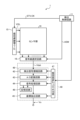
- FIG. 2 is a block diagram showing an example of the configuration of a detection device according to an embodiment.
- the detection device 1 further includes a detection control circuit 11 and a detection unit 40. Some or all of the functions of the detection control circuit 11 are included in the control circuit 122. In addition, some or all of the functions of the detection unit 40 other than the detection circuit 48 are included in the control circuit 122.
- the sensor unit 10 has multiple photodiodes PD.
- the photodiodes PD of the sensor unit 10 output an electrical signal corresponding to the irradiated light as a detection signal Vdet to the signal line selection circuit 16.
- the sensor unit 10 also performs detection according to the gate drive signal VGL supplied from the gate line drive circuit 15.
- the detection control circuit 11 is a circuit that supplies control signals to the gate line drive circuit 15, the signal line selection circuit 16, and the detection unit 40, respectively, and controls their operation.
- the detection control circuit 11 supplies various control signals, such as a start signal STV and a clock signal CK, to the gate line drive circuit 15.
- the detection control circuit 11 also supplies various control signals, such as a selection signal ASW, to the signal line selection circuit 16.
- the detection control circuit 11 also supplies various control signals to the light sources 53 and 54, controlling their lighting and non-lighting.
- the gate line driving circuit 15 is a circuit that drives multiple gate lines GL (see FIG. 3) based on various control signals.
- the gate line driving circuit 15 selects multiple gate lines GL sequentially or simultaneously, and supplies a gate driving signal VGL to the selected gate lines GL. In this way, the gate line driving circuit 15 selects multiple photodiodes PD connected to the gate lines GL.
- the signal line selection circuit 16 is a switch circuit that sequentially or simultaneously selects multiple signal lines SL (see FIG. 3).
- the signal line selection circuit 16 is, for example, a multiplexer.
- the signal line selection circuit 16 connects the selected signal line SL to the detection circuit 48 based on the selection signal ASW supplied from the detection control circuit 11. As a result, the signal line selection circuit 16 outputs the detection signal Vdet of the photodiode PD to the detection unit 40.
- the detection unit 40 includes a detection circuit 48, a signal processing circuit 44, a coordinate extraction circuit 45, a memory circuit 46, and a detection timing control circuit 47.
- the detection timing control circuit 47 controls the detection circuit 48, the signal processing circuit 44, and the coordinate extraction circuit 45 to operate in synchronization based on a control signal supplied from the detection control circuit 11.
- the detection circuit 48 is, for example, an analog front-end circuit (AFE).
- the detection circuit 48 is a signal processing circuit having at least the functions of a detection signal amplifier circuit 42 and an A/D conversion circuit 43.
- the detection signal amplifier circuit 42 amplifies the detection signal Vdet.
- the A/D conversion circuit 43 converts the analog signal output from the detection signal amplifier circuit 42 into a digital signal.
- the signal processing circuit 44 is a logic circuit that detects a predetermined physical quantity input to the sensor unit 10 based on the output signal of the detection circuit 48. When a finger is in contact with or close to the detection surface, the signal processing circuit 44 can detect unevenness on the surface of the finger or palm based on the signal from the detection circuit 48. The signal processing circuit 44 can also detect information about the living body based on the signal from the detection circuit 48. The information about the living body is, for example, an image of the blood vessels in the finger or palm, pulse waves, pulse rate, blood oxygen concentration, etc.
- the memory circuit 46 temporarily stores the signal calculated by the signal processing circuit 44.
- the memory circuit 46 may be, for example, a RAM (Random Access Memory), a register circuit, etc.
- the coordinate extraction circuit 45 is a logic circuit that determines the detection coordinates of the unevenness of the surface of a finger, etc., when the signal processing circuit 44 detects contact or proximity of a finger.
- the coordinate extraction circuit 45 is also a logic circuit that determines the detection coordinates of the blood vessels of the finger or palm.
- the coordinate extraction circuit 45 combines the detection signals Vdet output from each photodiode PD of the sensor unit 10 to generate two-dimensional information indicating the shape of the unevenness of the surface of the finger, etc., and two-dimensional information indicating the shape of the blood vessels of the finger or palm.
- the coordinate extraction circuit 45 may output the detection signal Vdet as the sensor output voltage Vo without calculating the detection coordinates.
- FIG. 3 is a circuit diagram showing a detection device according to an embodiment. Note that FIG. 3 also shows the circuit configuration of a detection circuit 48.
- a sensor pixel PX includes a photodiode PD, a capacitance element Ca, and a drive transistor Tr.
- the capacitance element Ca is a capacitance (sensor capacitance) formed in the photodiode PD, and is equivalently connected in parallel with the photodiode PD.
- FIG. 3 of the multiple gate lines GL, two gate lines GL(m) and GL(m+1) aligned in the second direction Dy are shown. Also, of the multiple signal lines SL, two signal lines SL(n) and SL(n+1) aligned in the first direction Dx are shown.
- the sensor pixel PX is the area surrounded by the gate line GL and the signal line SL.
- the drive transistor Tr is provided corresponding to each of the multiple photodiodes PD.
- the drive transistor Tr is composed of a thin film transistor, and in this example, is composed of an n-channel MOS (Metal Oxide Semiconductor) type TFT (Thin Film Transistor).
- Each of the multiple gate lines GL is connected to the gates of multiple drive transistors Tr arranged in a first direction Dx.
- Each of the multiple signal lines SL is connected to one of the sources and drains of multiple drive transistors Tr arranged in a second direction Dy.
- the other of the sources and drains of the multiple drive transistors Tr is connected to the cathode of the photodiode PD and the capacitance element Ca.
- the anode of the photodiode PD is supplied with a sensor power supply signal VDDSNS from the power supply circuit 123 (see FIG. 1).
- the signal line SL and the capacitance element Ca are supplied with a sensor reference voltage COM, which is the initial potential of the signal line SL and the capacitance element Ca, from the power supply circuit 123 via the reset transistor TrR.
- the switch SSW of the detection circuit 48 is turned on and connected to the signal line SL.
- the detection signal amplifier circuit 42 of the detection circuit 48 converts the current or charge supplied from the signal line SL into a voltage corresponding to the current or charge.
- a reference potential (Vref) having a fixed potential is input to the non-inverting input section (+) of the detection signal amplifier circuit 42, and the signal line SL is connected to the inverting input section (-).
- a signal equal to the sensor reference voltage COM is input as the reference potential (Vref) voltage.
- the control circuit 122 see FIG.
- the detection signal amplifier circuit 42 also has a capacitance element Cb and a reset switch RSW. During the reset period, the reset switch RSW is turned on and the charge of the capacitance element Cb is reset.
- the driving transistor Tr is not limited to an n-type TFT, and may be a p-type TFT.
- the pixel circuit of the sensor pixel PX shown in FIG. 3 is merely an example, and the sensor pixel PX may be provided with multiple transistors corresponding to one photodiode PD.
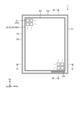
- Figure 4 is a plan view that shows a schematic configuration of the lower electrode, lower buffer layer, active layer, upper buffer layer, and upper electrode of multiple photodiodes.
- multiple photodiodes PD (organic photosensors) are arranged in a matrix in the detection area AA.
- the multiple photodiodes PD have a lower electrode 31, a lower buffer layer 32, an active layer 33, an upper buffer layer 34, an upper metal layer 35M, and an upper electrode 35.
- the multiple lower electrodes 31 are provided separately for each of the multiple photodiodes PD and are arranged in a matrix in the detection area AA.
- the lower buffer layer 32, the active layer 33, the upper buffer layer 34, and the upper metal layer 35M are provided continuously across the multiple photodiodes PD and are provided throughout the entire detection area AA.
- the upper electrode 35 is provided continuously across multiple photodiodes PD, and is provided in the detection area AA and the peripheral area GA.
- the upper electrode 35 is provided to cover the lower buffer layer 32, the active layer 33, the upper buffer layer 34, and the upper metal layer 35M.
- the outer edge of the upper electrode 35 is located outside (toward the outer edge of the substrate 21) the outer edges of the lower buffer layer 32, the active layer 33, the upper buffer layer 34, and the upper metal layer 35M.
- a part of the upper electrode 35 is connected to a contact portion CN provided in the peripheral area GA, and is electrically connected to an external circuit (for example, the control circuit 122 or the power supply circuit 123 (see FIG. 1)) through wiring on the substrate 21.
- the detection device 1 has a sealing film 90 that covers the multiple photodiodes PD.
- the sealing film 90 is provided across the detection area AA and the peripheral area GA, and is provided up to the outer edge side of the substrate 21.
- the sealing film 90 is provided to cover the multiple photodiodes PD.
- the outer edge of the sealing film 90 is located outside the outer edge of the upper electrode 35 (on the outer edge side of the substrate 21).
- the wiring board 71 (see FIG. 1) is not shown in FIG. 4, the wiring board 71 is connected to a terminal provided on the substrate 21 outside the upper electrode 35.
- the sealing film 90 may have an opening at the connection point between the wiring board 71 and the terminal, if necessary.
- Figure 5 is a cross-sectional view taken along line V-V' in Figure 4.
- Figure 6 is a cross-sectional view taken along line VI-VI' in Figure 4.
- the direction perpendicular to the surface of the substrate 21, from the substrate 21 toward the sealing film 90 is referred to as the "upper side” or simply “upper”.
- the direction from the sealing film 90 toward the substrate 21 is referred to as the "lower side” or simply “lower”.
- the detection device 1 has a substrate 21, a TFT layer 22, an organic insulating film 26, a barrier film 27, a photodiode PD, and a sealing film 90.
- the TFT layer 22, the organic insulating film 26, the barrier film 27, the photodiode PD, and the sealing film 90 are stacked in this order on the substrate 21.
- the substrate 21 is an insulating substrate formed from a film-like resin.
- the TFT layer 22 is a circuit formation layer in which the pixel circuits of the sensor pixels PX (see FIG. 3) are formed.
- the TFT layer 22 includes various wiring such as the drive transistors Tr, gate lines GL, and signal lines SL, as well as multiple inorganic insulating films that provide insulation between layers.
- the organic insulating film 26 is provided to cover the drive transistor Tr formed in the TFT layer 22.
- the organic insulating film 26 is a planarization film formed from an organic insulating material.
- the barrier film 27 is provided on the organic insulating film 26.
- the barrier film 27 is formed from an inorganic insulating material such as a silicon nitride film (SiN).
- the photodiode PD is provided on the barrier film 27.
- the photodiode PD is stacked in the following order, perpendicular to the substrate 21: lower electrode 31, lower buffer layer 32, active layer 33, upper buffer layer 34, upper metal layer 35M, and upper electrode 35.
- the photodiode PD of this embodiment is an organic photodiode (OPD) that uses an organic semiconductor as the active layer 33.
- OPD organic photodiode
- the lower electrode 31 is formed of a conductive material having light transmissivity, such as ITO (Indium Tin Oxide).
- the lower buffer layer 32, the active layer 33, the upper buffer layer 34, the upper metal layer 35M, and the upper electrode 35 are provided continuously across multiple photodiodes PD. Specifically, the lower buffer layer 32, the active layer 33, the upper buffer layer 34, the upper metal layer 35M, and the upper electrode 35 are provided overlapping the lower electrode 31, and are also provided in the region between adjacent lower electrodes 31.
- the insulating film 36 is provided to cover the periphery of the lower electrode 31.
- the insulating film 36 insulates the lower electrodes 31 of adjacent photodiodes PD. Even if a step occurs in the lower buffer layer 32 at the periphery of the lower electrode 31, the insulating film 36 is provided, so that the occurrence of a short circuit between the active layer 33 and the lower electrode 31 can be suppressed.
- the insulating film 36 is formed of an inorganic insulating material such as a silicon nitride film (SiN) or a silicon oxide film (SiO 2 ).
- the insulating film 36 is provided to cover the periphery of the contact portion CN.
- the insulating film 36 is provided to cover the entire barrier film 27, but is not limited thereto, and may be provided to cover at least the periphery of the lower electrode 31 and the periphery of the contact portion CN.
- the active layer 33 changes its characteristics (for example, voltage-current characteristics and resistance value) depending on the light irradiated thereto.
- An organic material is used as the material of the active layer 33.
- the active layer 33 has a bulk heterostructure in which a p-type organic semiconductor and an n-type fullerene derivative (PCBM) which is an n-type organic semiconductor are mixed.
- PCBM n-type fullerene derivative
- low molecular weight organic materials such as C 60 (fullerene), PCBM (phenyl C 61 -butyric acid methyl ester), CuPc (copper phthalocyanine), F 16 CuPc (fluorinated copper phthalocyanine) , rubrene (5,6,11,12-tetraphenyltetracene), and PDI (perylene derivative) can be used as the active layer 33.
- C 60 fulllerene
- PCBM phenyl C 61 -butyric acid methyl ester
- CuPc copper phthalocyanine
- F 16 CuPc fluorinated copper phthalocyanine
- rubrene 5,6,11,12-tetraphenyltetracene
- PDI perylene derivative
- the active layer 33 can be formed by a deposition type (dry process) using these low molecular weight organic materials.
- the active layer 33 may be, for example, a laminated film of CuPc and F 16 CuPc, or a laminated film of rubrene and C 60.
- the active layer 33 can also be formed by a coating type (wet process).
- the active layer 33 is made of a material that combines the above-mentioned low molecular weight organic material and a polymer organic material.
- the polymer organic material for example, P3HT (poly(3-hexylthiophene)), F8BT (F8-alt-benzothiadiazole), etc. can be used.
- the active layer 33 can be a film in a state where P3HT and PCBM are mixed, or a film in a state where F8BT and PDI are mixed.
- the active layer 33 is not limited to a bulk heterostructure and may be a PIN type.
- the lower buffer layer 32 and the upper buffer layer 34 are provided to facilitate the holes and electrons generated in the active layer 33 reaching the lower electrode 31 or the upper electrode 35.
- the lower buffer layer 32 is provided between the lower electrode 31 and the active layer 33, and is in direct contact with the lower electrode 31 and the active layer 33.
- the lower buffer layer 32 is also provided between adjacent lower electrodes 31, covering the barrier film 27 and the insulating film 36.
- the upper buffer layer 34 is provided between the active layer 33 and the upper electrode 35.
- the upper metal layer 35M is provided between the upper buffer layer 34 and the upper electrode 35.
- the upper buffer layer 34 is in direct contact with the active layer 33 and the upper metal layer 35M.
- the lower electrode 31 is the cathode electrode of the photodiode PD
- the upper electrode 35 is the anode electrode of the photodiode PD
- the lower buffer layer 32 is an electron transport layer
- the upper buffer layer 34 is a hole transport layer.
- the material of the electron transport layer is ethoxylated polyethyleneimine (PEIE).
- PEIE polyethyleneimine
- the material of the hole transport layer is a metal oxide layer.
- tungsten oxide (WO 3 ), molybdenum oxide, or the like is used as the metal oxide layer.
- the lower electrode 31 may be the anode electrode of the photodiode PD, and the upper electrode 35 may be the cathode electrode of the photodiode PD.
- the lower buffer layer 32 may be a hole transport layer, and the upper buffer layer 34 may be an electron transport layer.
- the upper metal layer 35M is formed to have the same width (area) as the lower buffer layer 32, the active layer 33, and the upper buffer layer 34.
- the upper metal layer 35M functions as the upper electrode of the photodiode PD and also functions as a mask when patterning the lower buffer layer 32, the active layer 33, and the upper buffer layer 34.
- the manufacturing process of the photodiode PD will be described later with reference to FIG. 7.
- the side surfaces of the photodiode PD are shown as being perpendicular to the surface of the substrate 21.
- the side surfaces 32s, 33s, 34s, and 35Ms of the photodiode PD have a forward tapered shape (see the enlarged view in Figure 8).
- the upper electrode 35 covers the top surface of the upper metal layer 35M, as well as the side surface 32s of the lower buffer layer 32, the side surface 33s of the active layer 33, the side surface 34s of the upper buffer layer 34, and the side surface 35Ms of the upper metal layer 35M.
- side surface 32s of the lower buffer layer 32, side surface 33s of the active layer 33, side surface 34s of the upper buffer layer 34, and side surface 35Ms of the upper metal layer 35M may be referred to as "side surfaces 32s, 33s, 34s, 35Ms of the photodiode PD.”
- the upper electrode 35 includes an overlapping portion 35a, a side portion 35b, and an extending portion 35c.
- the overlapping portion 35a covers the upper surface of the upper metal layer 35M.
- the side portion 35b covers the side surfaces 32s, 33s, 34s, and 35Ms of the photodiode PD.
- the upper end of the side portion 35b is connected to the overlapping portion 35a, and the lower end of the side portion 35b is connected to the extending portion 35c.
- the extending portion 35c extends to the peripheral area GA outside the side surfaces 32s, 33s, 34s, and 35Ms of the multiple photodiodes PD.
- the extending portion 35c of the upper electrode 35 is provided on the barrier film 27 and the insulating film 36 in a region that does not overlap with the multiple photodiodes PD.
- the side surface 35s on the outer edge of the upper electrode 35 (side surface 35s of extension portion 35c) is located closer to the outer edge of the substrate 21 than the side surfaces 32s, 33s, 34s, 35Ms of the multiple photodiodes PD.
- the planar area of the upper electrode 35 is larger than the planar areas of the lower buffer layer 32, the active layer 33, the upper buffer layer 34, and the upper metal layer 35M.
- the side surface 35s of the upper electrode 35 is located closer to the detection area AA than the side surface of the barrier film 27. Also, as shown in FIG. 6, a portion of the extension portion 35c of the upper electrode 35 extends to an area overlapping with the contact portion CN and is connected to the contact portion CN.
- the upper electrode 35 is formed of a conductive material having translucency, such as ITO or IZO. Without being limited thereto, the upper electrode 35 may be formed of a conductive material having no translucency, such as silver (Ag).
- the upper metal layer 35M is formed of a metal material, such as silver (Ag). In other words, the upper metal layer 35M may be made of the same metal material as the upper electrode 35.
- the sealing film 90 is provided to cover the multiple photodiodes PD.
- the sealing film 90 is provided to cover the overlapping portion 35a, side portion 35b, and extension portion 35c of the upper electrode 35.
- the side surface of the sealing film 90 is located closer to the outer edge of the substrate 21 than the side surface 35s on the outer edge side of the upper electrode 35.
- the sealing film 90 effectively seals the photodiodes PD and can prevent moisture from entering from the outside.
- the sealing film 90 covers the side surface 35s on the outer edge side of the upper electrode 35, it can effectively prevent moisture from entering from the outer edge side of the substrate 21 compared to when the upper electrode 35 extends to the outer edge side of the substrate 21.
- the sealing film 90 is formed of an inorganic film such as a silicon nitride film or an aluminum oxide film.
- the sealing film 90 is not limited to a single layer film, but may be a laminated film in which multiple inorganic films are stacked. Alternatively, the sealing film 90 may be a laminated film in which an organic film formed of a resin film such as acrylic and an inorganic film are stacked.
- the side surfaces 32s, 33s, 34s, and 35Ms of the lower buffer layer 32, active layer 33, upper buffer layer 34, and upper metal layer 35M are covered with the upper electrode 35. This makes it possible to suppress contact between the patterning mask and the active layer 33 when forming the upper electrode 35, compared to when the upper electrode 35 is formed in the same shape as the lower buffer layer 32, active layer 33, and upper buffer layer 34.
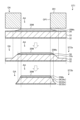
- Fig. 7 is an explanatory diagram that shows a schematic diagram of the manufacturing process of the detection device according to the first embodiment.
- Fig. 8 is an explanatory diagram that shows an enlarged view of steps ST1 and ST2 in Fig. 7. Note that in Fig. 7, the lower buffer layer 32 and the upper buffer layer 34 are omitted in order to make the drawing easier to see.
- a TFT layer 22, an organic insulating film 26, and a barrier film 27 are formed on a substrate 21.
- the lower electrode 31 is patterned in a matrix shape corresponding to the arrangement of the multiple photodiodes PD.
- the lower buffer layer 32, the active layer 33, and the upper buffer layer 34 are formed over the entire surface of the substrate 21, across the detection area AA and the peripheral area GA.
- a film forming device uses a first patterning mask 201 to form an upper metal layer 35M on the upper buffer layer 34 in an area corresponding to the detection area AA of the substrate 21 (step ST1).
- the first patterning mask 201 for forming the upper metal layer 35M is a metal mask having an opening OP1.
- the opening OP1 is provided at a position overlapping with the area (detection area AA) where multiple photodiodes PD are to be formed.
- the upper metal layer 35M is formed by sputtering, vapor deposition, plasma CVD, or the like.
- the first patterning mask 201 is positioned above and spaced apart from the upper buffer layer 34.
- the upper metal layer 35M is deposited around the opening OP1 of the first patterning mask 201 to the outside.
- the side surface 35Ms of the upper metal layer 35M is formed to have a forward tapered shape.
- the lower buffer layer 32, the active layer 33, and the upper buffer layer 34 are removed from the regions where the upper metal layer 35M is not provided (step ST2).
- the upper metal layer 35M is used as a mask.
- the lower buffer layer 32, the active layer 33, and the upper buffer layer 34 in the regions that do not overlap with the upper metal layer 35M are removed by dry etching.
- the lower buffer layer 32, the active layer 33, and the upper buffer layer 34 in the regions that overlap with the upper metal layer 35M are formed as a plurality of photodiodes PD.
- etching of the lower buffer layer 32, the active layer 33, and the upper buffer layer 34 first proceeds in the region outside the side surface 35Ms of the upper metal layer 35M.
- the thin outer edge portion the portion overlapping the side surface 35Ms of the upper metal layer 35M is also etched.
- step ST2b of FIG. 8 when the outer edge portion of the upper metal layer 35M is further removed, etching of the lower buffer layer 32, active layer 33, and upper buffer layer 34 proceeds sequentially in the areas overlapping with the removed portion of the upper metal layer 35M.
- the side surfaces 32s, 33s, and 34s of the lower buffer layer 32, active layer 33, and upper buffer layer 34 of the photodiode PD are formed to have a forward tapered shape.
- the side surface 35Ms of the upper metal layer 35M is also formed to have a forward tapered shape.
- a film forming apparatus uses a second patterning mask 202 to form an upper electrode 35 on the upper metal layer 35M (step ST3).
- the second patterning mask 202 for forming the upper electrode 35 is a metal mask having an opening OP2.
- the opening OP2 of the second patterning mask 202 has a width W2 that is at least greater than the width W1 of the active layer 33.
- the width W1 of the active layer 33 is the maximum width between the side surfaces 33s of the active layer 33.
- the active layer 33 has a forward tapered shape, and the maximum width W1 of the active layer 33 is the distance at the portion where the lower end of the side surface 33s of the active layer 33 contacts the insulating film 36 or the barrier film 27.
- the distance L1 between the inner wall of the opening OP2 of the second patterning mask 202 and the side surface 33s of the active layer 33 is 500 ⁇ m or more. More specifically, the distance L1 is the distance between the inner wall of the opening OP2 of the second patterning mask 202 and the lower end of the side surface 33s of the active layer 33, which contacts the insulating film 36 or the barrier film 27, in a direction parallel to the surface of the substrate 21. The distance L1 is different for each side of the photodiode PD depending on the alignment accuracy of the second patterning mask 202. For example, as shown in FIG.
- the distance L1 between the inner wall of the opening OP2 and the side surface 33s of the active layer 33 is larger than the distance L1 on the opposite side.
- the second patterning mask 202 is arranged so that the minimum distance L1 among the distances L1 along the outer edge of the photodiode PD is 500 ⁇ m or more.
- the width W2 of the opening OP2 is smaller than the width of the barrier film 27 formed on the substrate 21.
- the inner wall of the opening OP2 of the second patterning mask 202 overlaps with the outer edge side of the barrier film 27 formed on the substrate 21.
- the upper electrode 35 is formed to cover the top surface of the upper metal layer 35M, as well as the side surfaces 32s, 33s, 34s of the photodiode PD and the side surface 35Ms of the upper metal layer 35M.
- the upper electrode 35 is provided extending further to the outer edge side of the substrate 21 than the side surface 33s of the active layer 33.
- the side surface 35s on the outer edge side of the upper electrode 35 is formed inside (towards the detection area AA) than the side surface of the barrier film 27.
- a film forming device forms a sealing film 90 covering the upper electrode 35 (step ST4).
- a patterning mask (not shown) for forming the sealing film 90 has an opening with a width larger than the opening OP2.
- the sealing film 90 is formed covering the entire surface of the upper electrode 35.
- the side surface 35s on the outer edge side of the upper electrode 35 is also covered by the sealing film 90.
- the side surface 35s on the outer edge side of the upper electrode 35 is formed inside (towards the detection area AA) more than the side surface of the sealing film 90.
- the detection device 1 of this embodiment is formed by the above-mentioned process.
- the inner wall of the opening OP2 of the second patterning mask 202 is positioned at a predetermined distance L1 from the side surface 33s of the active layer 33. This makes it possible to suppress contact between the second patterning mask 202 and the side surface 33s of the active layer 33, compared to when the upper electrode 35 is formed in the same shape as the lower buffer layer 32, the active layer 33, and the upper buffer layer 34, i.e., when the side surface 35s of the upper electrode 35 is provided at a position overlapping the side surfaces 32s, 33s, 34s, and 35Ms of the photodiode PD.
- the manufacturing process of the detection device 1 shown in Figures 7 and 8 is merely a schematic illustration and can be modified as appropriate.
- the layered structure and forward tapered shapes of the side surfaces 32s, 33s, and 34s shown in Figure 8 are shown exaggerated to make it easier to understand, and the film thickness, inclination, width, etc. of the side surfaces 32s, 33s, and 34s may be different.
- Second Embodiment 9 is an explanatory diagram showing a manufacturing process of the detection device according to the second embodiment.
- the same components as those described in the above embodiment are denoted by the same reference numerals, and duplicated description will be omitted.
- the lower buffer layer 32 and the upper buffer layer 34 are omitted, as in FIG. 7.
- the manufacturing process shown in FIG. 9 corresponds to the process (step ST3) of forming the upper electrode 35 in FIG. 7.
- the processes of depositing the upper metal layer 35M, removing the active layer 33, and depositing the sealing film 90 are similar to the processes of steps ST1, ST2, and ST4 described above in FIG. 7, and repeated explanations will be omitted.
- the second patterning mask 202 is supported on spacers 203 provided on the outer edge side of the substrate 21.
- the height of the spacers 203 is greater than the total height of the lower buffer layer 32, the active layer 33, the upper buffer layer 34, and the upper metal layer 35M.
- the spacers 203 are resin tapes made of a resin material such as polyimide.
- the second patterning mask 202 is disposed above the upper metal layer 35M. More specifically, in the direction perpendicular to the substrate 21, the lower surface of the second patterning mask 202 is disposed at a distance from the upper surface of the upper metal layer 35M.
- the width W2 of the opening OP2 of the second patterning mask 202 is at least greater than the width W1 of the active layer 33.
- the inner wall of the opening OP2 of the second patterning mask 202 may be positioned so as to overlap the side surface 33s of the active layer 33.
- the distance L1 (see FIG. 7) between the inner wall of the opening OP2 of the second patterning mask 202 and the side surface 33s of the active layer 33 may be 500 ⁇ m or less.
- a film forming device uses the second patterning mask 202 to form the upper electrode 35 on the upper metal layer 35M (step ST3A).
- the upper electrode 35 is formed between the lower surface of the second patterning mask 202 and the upper surface of the upper metal layer 35M.
- the upper electrode 35 is formed to cover the upper surface of the upper metal layer 35M, as well as the side surfaces 32s, 33s, and 34s of the photodiode PD and the side surface 35Ms of the upper metal layer 35M.
- the second patterning mask 202 is supported by the spacers 203 during the deposition process of the upper electrode 35, so that contact between the second patterning mask 202 and the respective side surfaces 32s, 33s, and 34s of the lower buffer layer 32, active layer 33, and upper buffer layer 34 can be suppressed.
Landscapes
- Physics & Mathematics (AREA)
- Electromagnetism (AREA)
- Solid State Image Pick-Up Elements (AREA)
Abstract
検出装置は、基板と、基板の上に積層された有機絶縁膜及びバリア膜と、基板の検出領域で、バリア膜の上に、下部電極、下部バッファ層、活性層、上部バッファ層及び上部電極の順に積層された有機光センサと、有機光センサを覆う封止膜と、を有し、下部バッファ層、活性層及び上部バッファ層の側面は、上部電極で覆われており、上部電極は、封止膜で覆われている。
Description
本発明は、検出装置及び検出装置の製造方法に関する。
指紋パターンや静脈パターンを検出可能な光センサが知られている(例えば、特許文献1)。このような光センサは、活性層として有機半導体材料が用いられた複数のフォトダイオード(OPD:Organic Photodiode)を有する。特許文献2に記載されるように、フォトダイオードは、例えば、下部電極、電子輸送層、活性層、正孔輸送層、上部電極の順に積層される。電子輸送層又は正孔輸送層は、バッファ層とも呼ばれる。
OPDを有する検出装置の製造工程において、パターニング用マスクを用いた成膜工程で、パターニング用マスクと活性層等の膜面とが接触する場合がある。活性層等の膜面に傷や異物が付着すると、OPDの外縁側で膜厚ばらつきや形状ばらつきを引き起こす要因となる。この膜厚ばらつきや形状ばらつきが生じると、有機光センサに入射する光の状態が異なり、検出精度が低下する可能性がある。
特許文献3から特許文献5には、液晶表示装置の導電膜やカラーフィルタの成膜に用いられるマスクに関する技術が記載されている。しかし、特許文献3から特許文献5には、OPDを有する検出装置及びその製造方法について記載されていない。
本発明は、有機光センサの傷の発生や異物の付着を抑制することが可能な検出装置及び検出装置の製造方法を提供することを目的とする。
本発明の一態様の検出装置は、基板と、前記基板の上に積層された有機絶縁膜及びバリア膜と、前記基板の検出領域で、前記バリア膜の上に、下部電極、下部バッファ層、活性層、上部バッファ層及び上部電極の順に積層された有機光センサと、前記有機光センサを覆う封止膜と、を有し、前記下部バッファ層、前記活性層及び前記上部バッファ層の側面は、前記上部電極で覆われており、前記上部電極は、前記封止膜で覆われている。
本発明の一態様の検出装置の製造方法は、基板の上に、有機絶縁膜、バリア膜、下部電極、下部バッファ層、活性層、上部バッファ層の順に形成する工程と、第1パターニング用マスクを用いて、前記基板の検出領域に対応する領域で前記上部バッファ層の上に上部メタル層を形成し、前記上部メタル層が設けられていない領域で、前記下部バッファ層、前記活性層及び前記上部バッファ層を除去する工程と、第2パターニング用マスクを用いて、前記上部メタル層の上に上部電極を形成する工程と、を有し、前記上部電極を形成する工程で、前記第2パターニング用マスクの開口の内壁と、前記活性層の側面との距離は500μm以上であり、前記下部バッファ層、前記活性層及び前記上部バッファ層の側面は、前記上部電極で覆われる。
本発明の一態様の検出装置の製造方法は、基板の上に、有機絶縁膜、バリア膜、下部電極、下部バッファ層、活性層、上部バッファ層の順に形成する工程と、第1パターニング用マスクを用いて、前記基板の検出領域に対応する領域で前記上部バッファ層の上に上部メタル層を形成し、前記上部メタル層が設けられていない領域で、前記下部バッファ層、前記活性層及び前記上部バッファ層を除去する工程と、第2パターニング用マスクを用いて、前記上部メタル層の上に上部電極を形成する工程と、を有し、前記上部電極を形成する工程で、前記第2パターニング用マスクは、前記基板の外縁側に設けられたスペーサの上に支持され、前記下部バッファ層、前記活性層及び前記上部バッファ層の側面は、前記上部電極で覆われる。
本発明を実施するための形態(実施形態)につき、図面を参照しつつ詳細に説明する。以下の実施形態に記載した内容により本開示が限定されるものではない。また、以下に記載した構成要素には、当業者が容易に想定できるもの、実質的に同一のものが含まれる。さらに、以下に記載した構成要素は適宜組み合わせることが可能である。なお、開示はあくまで一例にすぎず、当業者において、本開示の主旨を保っての適宜変更について容易に想到し得るものについては、当然に本開示の範囲に含有されるものである。また、図面は説明をより明確にするため、実際の態様に比べ、各部の幅、厚さ、形状等について模式的に表される場合があるが、あくまで一例であって、本開示の解釈を限定するものではない。また、本開示と各図において、既出の図に関して前述したものと同様の要素には、同一の符号を付して、詳細な説明を適宜省略することがある。
本明細書及び特許請求の範囲において、ある構造体の上に他の構造体を配置する態様を表現するにあたり、単に「上に」と表記する場合、特に断りの無い限りは、ある構造体に接するように、直上に他の構造体を配置する場合と、ある構造体の上方に、さらに別の構造体を介して他の構造体を配置する場合との両方を含むものとする。
(第1実施形態)
図1は、第1実施形態に係る検出装置を模式的に示す平面図である。図1に示すように、検出装置1は、基板21と、センサ部10と、ゲート線駆動回路15と、信号線選択回路16と、検出回路48と、制御回路122と、電源回路123と、第1光源基材51と、第2光源基材52と、光源53、54と、を有する。第1光源基材51には、複数の光源53が設けられる。第2光源基材52には複数の光源54が設けられる。
図1は、第1実施形態に係る検出装置を模式的に示す平面図である。図1に示すように、検出装置1は、基板21と、センサ部10と、ゲート線駆動回路15と、信号線選択回路16と、検出回路48と、制御回路122と、電源回路123と、第1光源基材51と、第2光源基材52と、光源53、54と、を有する。第1光源基材51には、複数の光源53が設けられる。第2光源基材52には複数の光源54が設けられる。
基板21には、配線基板71を介して制御基板121が電気的に接続される。配線基板71は、例えばフレキシブルプリント基板やリジット基板である。配線基板71には、検出回路48が設けられている。制御基板121には、制御回路122及び電源回路123が設けられている。制御回路122は、例えばFPGA(Field Programmable Gate Array)である。制御回路122は、センサ部10、ゲート線駆動回路15及び信号線選択回路16に制御信号を供給して、センサ部10の検出動作を制御する。また、制御回路122は、光源53、54に制御信号を供給して、光源53、54の点灯又は非点灯を制御する。電源回路123は、センサ電源信号VDDSNS(図3参照)等の電圧信号をセンサ部10、ゲート線駆動回路15及び信号線選択回路16に供給する。また、電源回路123は、電源電圧を光源53、54に供給する。
基板21は、検出領域AAと、周辺領域GAとを有する。検出領域AAは、センサ部10が有する複数のフォトダイオードPD(図4参照)が設けられた領域である。周辺領域GAは、検出領域AAの外周と、基板21の外縁との間の領域であり、複数のフォトダイオードPDが設けられない領域である。
ゲート線駆動回路15及び信号線選択回路16は、周辺領域GAに設けられる。具体的には、ゲート線駆動回路15は、周辺領域GAのうち第2方向Dyに沿って延在する領域に設けられる。信号線選択回路16は、周辺領域GAのうち第1方向Dxに沿って延在する領域に設けられ、センサ部10と検出回路48との間に設けられる。
なお、以下の説明において、第1方向Dxは、基板21と平行な面内の一方向である。第2方向Dyは、基板21と平行な面内の一方向であり、第1方向Dxと直交する方向である。なお、第2方向Dyは、第1方向Dxと直交しないで交差してもよい。第3方向Dzは、第1方向Dx及び第2方向Dyと直交する方向であり、基板21の主面の法線方向である。また、「平面視」とは、基板21と垂直な方向から見た場合の位置関係をいう。
複数の光源53は、第1光源基材51に設けられ、第2方向Dyに沿って配列される。複数の光源54は、第2光源基材52に設けられ、第2方向Dyに沿って配列される。第1光源基材51及び第2光源基材52は、それぞれ、制御基板121に設けられた端子部124、125を介して、制御回路122及び電源回路123と電気的に接続される。
複数の光源53及び複数の光源54は、例えば、無機LED(Light Emitting Diode)や、有機EL(OLED:Organic Light Emitting Diode)等が用いられる。複数の光源53及び複数の光源54は、それぞれ異なる波長の光を出射する。
光源53から出射された第1光は、主に指等の被検出体の表面で反射されセンサ部10に入射する。これにより、センサ部10は、指等の表面の凹凸の形状を検出することで指紋を検出することができる。光源54から出射された第2光は、主に指等の内部で反射し又は指等を透過してセンサ部10に入射する。これにより、センサ部10は、指等の内部の生体に関する情報を検出できる。生体に関する情報とは、例えば、指や掌の脈波、脈拍、血管像等である。すなわち、検出装置1は、指紋を検出する指紋検出装置や、静脈などの血管パターンを検出する静脈検出装置として構成されてもよい。
なお、図1に示す光源53、54の配置は、あくまで一例であり適宜変更することができる。検出装置1は、光源として複数種類の光源53、54が設けられている。ただし、これに限定されず、光源は1種類であってもよい。例えば、第1光源基材51及び第2光源基材52のそれぞれに、複数の光源53及び複数の光源54が配置されていてもよい。また、光源53及び光源54が設けられる光源基材は1つ又は3つ以上であってもよい。あるいは、光源は、少なくとも1つ以上配置されていればよい。
図2は、実施形態に係る検出装置の構成例を示すブロック図である。図2に示すように、検出装置1は、さらに検出制御回路11と検出部40と、を有する。検出制御回路11の機能の一部又は全部は、制御回路122に含まれる。また、検出部40のうち、検出回路48以外の機能の一部又は全部は、制御回路122に含まれる。
センサ部10は、複数のフォトダイオードPDを有する。センサ部10が有するフォトダイオードPDは、照射される光に応じた電気信号を、検出信号Vdetとして信号線選択回路16に出力する。また、センサ部10は、ゲート線駆動回路15から供給されるゲート駆動信号VGLにしたがって検出を行う。
検出制御回路11は、ゲート線駆動回路15、信号線選択回路16及び検出部40にそれぞれ制御信号を供給し、これらの動作を制御する回路である。検出制御回路11は、スタート信号STV、クロック信号CK等の各種制御信号をゲート線駆動回路15に供給する。また、検出制御回路11は、選択信号ASW等の各種制御信号を信号線選択回路16に供給する。また、検出制御回路11は、各種制御信号を光源53、54に供給して、それぞれの点灯及び非点灯を制御する。
ゲート線駆動回路15は、各種制御信号に基づいて複数のゲート線GL(図3参照)を駆動する回路である。ゲート線駆動回路15は、複数のゲート線GLを順次又は同時に選択し、選択されたゲート線GLにゲート駆動信号VGLを供給する。これにより、ゲート線駆動回路15は、ゲート線GLに接続された複数のフォトダイオードPDを選択する。
信号線選択回路16は、複数の信号線SL(図3参照)を順次又は同時に選択するスイッチ回路である。信号線選択回路16は、例えばマルチプレクサである。信号線選択回路16は、検出制御回路11から供給される選択信号ASWに基づいて、選択された信号線SLと検出回路48とを接続する。これにより、信号線選択回路16は、フォトダイオードPDの検出信号Vdetを検出部40に出力する。
検出部40は、検出回路48と、信号処理回路44と、座標抽出回路45と、記憶回路46と、検出タイミング制御回路47と、を備える。検出タイミング制御回路47は、検出制御回路11から供給される制御信号に基づいて、検出回路48と、信号処理回路44と、座標抽出回路45と、が同期して動作するように制御する。
検出回路48は、例えばアナログフロントエンド回路(AFE、Analog Front End)である。検出回路48は、少なくとも検出信号増幅回路42及びA/D変換回路43の機能を有する信号処理回路である。検出信号増幅回路42は、検出信号Vdetを増幅する。A/D変換回路43は、検出信号増幅回路42から出力されるアナログ信号をデジタル信号に変換する。
信号処理回路44は、検出回路48の出力信号に基づいて、センサ部10に入力された所定の物理量を検出する論理回路である。信号処理回路44は、指が検出面に接触又は近接した場合に、検出回路48からの信号に基づいて指や掌の表面の凹凸を検出できる。また、信号処理回路44は、検出回路48からの信号に基づいて生体に関する情報を検出できる。生体に関する情報は、例えば、指や掌の血管像、脈波、脈拍、血中酸素濃度等である。
記憶回路46は、信号処理回路44で演算された信号を一時的に保存する。記憶回路46は、例えばRAM(Random Access Memory)、レジスタ回路等であってもよい。
座標抽出回路45は、信号処理回路44において指の接触又は近接が検出されたときに、指等の表面の凹凸の検出座標を求める論理回路である。また、座標抽出回路45は、指や掌の血管の検出座標を求める論理回路である。座標抽出回路45は、センサ部10の各フォトダイオードPDから出力される検出信号Vdetを組み合わせて、指等の表面の凹凸の形状を示す二次元情報及び指や掌の血管の形状を示す二次元情報を生成する。なお、座標抽出回路45は、検出座標を算出せずにセンサ出力電圧Voとして検出信号Vdetを出力してもよい。
図3は、実施形態に係る検出装置を示す回路図である。なお、図3では、検出回路48の回路構成も併せて示している。図3に示すように、センサ画素PXは、フォトダイオードPDと、容量素子Caと、駆動トランジスタTrとを含む。容量素子Caは、フォトダイオードPDに形成される容量(センサ容量)であり、等価的にフォトダイオードPDと並列に接続される。
図3では、複数のゲート線GLのうち、第2方向Dyに並ぶ2つのゲート線GL(m)、GL(m+1)を示す。また、複数の信号線SLのうち、第1方向Dxに並ぶ2つの信号線SL(n)、SL(n+1)を示す。センサ画素PXは、ゲート線GLと信号線SLとで囲まれた領域である。
駆動トランジスタTrは、複数のフォトダイオードPDのそれぞれに対応して設けられる。駆動トランジスタTrは、薄膜トランジスタにより構成されるものであり、この例では、nチャネルのMOS(Metal Oxide Semiconductor)型のTFT(Thin Film Transistor)で構成されている。
複数のゲート線GLのそれぞれは、第1方向Dxに配列された複数の駆動トランジスタTrのゲートに接続される。複数の信号線SLのそれぞれは、第2方向Dyに配列された複数の駆動トランジスタTrのソース及びドレインの一方に接続される。複数の駆動トランジスタTrのソース及びドレインの他方は、フォトダイオードPDのカソード及び容量素子Caに接続される。
フォトダイオードPDのアノードには、電源回路123(図1参照)からセンサ電源信号VDDSNSが供給される。また、信号線SL及び容量素子Caには、電源回路123からリセットトランジスタTrRを介して、信号線SL及び容量素子Caの初期電位となるセンサ基準電圧COMが供給される。
露光期間でセンサ画素PXに光が照射されると、フォトダイオードPDには光量に応じた電流が流れ、これにより容量素子Caに電荷が蓄積される。読み出し期間で駆動トランジスタTrがオンになると、容量素子Caに蓄積された電荷に応じて、信号線SLに電流が流れる。信号線SLは、信号線選択回路16の出力トランジスタTrSを介して検出回路48に接続される。これにより、検出装置1は、センサ画素PXごとにフォトダイオードPDに照射される光の光量に応じた信号を検出できる。
検出回路48は、読み出し期間にスイッチSSWがオンになり、信号線SLと接続される。検出回路48の検出信号増幅回路42は、信号線SLから供給された電流または電荷に応じた電圧に変換する。検出信号増幅回路42の非反転入力部(+)には、固定された電位を有する基準電位(Vref)が入力され、反転入力部(-)には、信号線SLが接続される。実施形態では、基準電位(Vref)電圧としてセンサ基準電圧COMと同じ信号が入力される。制御回路122(図1参照)は、光が照射された場合の検出信号Vdetと、光が照射されていない場合の検出信号Vdetとの差分をセンサ出力電圧Voとして演算する。また、検出信号増幅回路42は、容量素子Cb及びリセットスイッチRSWを有する。リセット期間においてリセットスイッチRSWがオンになり、容量素子Cbの電荷がリセットされる。
なお、駆動トランジスタTrは、n型TFTに限定されず、p型TFTで構成されてもよい。また、図3に示すセンサ画素PXの画素回路はあくまで一例であり、センサ画素PXには、1つのフォトダイオードPDに対応して、複数のトランジスタが設けられていてもよい。
次に、図4から図6を参照して、フォトダイオードPDの構成について説明する。図4は、複数のフォトダイオードが有する下部電極、下部バッファ層、活性層、上部バッファ層及び上部電極の構成を模式的に示す平面図である。
図4に示すように、複数のフォトダイオードPD(有機光センサ)は、検出領域AAにマトリクス状に配置される。複数のフォトダイオードPDは、下部電極31と、下部バッファ層32と、活性層33と、上部バッファ層34と、上部メタル層35Mと、上部電極35と、を有する。複数の下部電極31は、複数のフォトダイオードPDごとに離隔して設けられ、検出領域AAにマトリクス状に配置される。下部バッファ層32、活性層33、上部バッファ層34及び上部メタル層35Mは、複数のフォトダイオードPDに亘って連続して設けられ、検出領域AA全体に設けられる。
上部電極35は複数のフォトダイオードPDに亘って連続して設けられ、検出領域AA及び周辺領域GAに設けられる。上部電極35は、下部バッファ層32、活性層33、上部バッファ層34及び上部メタル層35Mを覆って設けられる。また、上部電極35の外縁は、下部バッファ層32、活性層33、上部バッファ層34及び上部メタル層35Mの外縁よりも外側(基板21の外縁側)に位置する。上部電極35の一部は周辺領域GAに設けられたコンタクト部CNに接続され、基板21の配線を通して、外部回路(例えば制御回路122や電源回路123(図1参照))に電気的に接続される。
検出装置1は、複数のフォトダイオードPDを覆う封止膜90を有する。封止膜90は、検出領域AA及び周辺領域GAに亘って設けられ、基板21の外縁側まで設けられる。封止膜90は、複数のフォトダイオードPDを覆って設けられる。封止膜90の外縁は、上部電極35の外縁よりも外側(基板21の外縁側)に位置する。
なお、図4では配線基板71(図1参照)の図示を省略しているが、配線基板71は、上部電極35の外側で基板21に設けられた端子と接続される。また、封止膜90には必要に応じて、配線基板71と端子との接続箇所に開口が設けられていてもよい。
次に、検出装置1の複数のフォトダイオードPD及び封止膜90の積層構造について説明する。図5は、図4のV-V’断面図である。図6は、図4のVI-VI’断面図である。
なお、以下の説明では、基板21の表面に垂直な方向において、基板21から封止膜90に向かう方向を「上側」又は単に「上」とする。また、封止膜90から基板21に向かう方向を「下側」又は単に「下」とする。
図5及び図6に示すように、検出装置1は、基板21、TFT層22、有機絶縁膜26、バリア膜27、フォトダイオードPD、及び、封止膜90を有する。検出領域AAで、基板21の上にTFT層22、有機絶縁膜26、バリア膜27、フォトダイオードPD、封止膜90の順に積層される。
基板21は、フィルム状の樹脂で形成された絶縁性基板である。TFT層22は、センサ画素PX(図3参照)が有する画素回路が形成された回路形成層である。TFT層22は、駆動トランジスタTr、ゲート線GL、信号線SL等の各種配線、及び、層間を絶縁する複数の無機絶縁膜を含む。
有機絶縁膜26は、TFT層22に形成された駆動トランジスタTrを覆って設けられる。有機絶縁膜26は、有機絶縁材料で形成された平坦化膜である。バリア膜27は、有機絶縁膜26の上に設けられる。バリア膜27は、例えばシリコン窒化膜(SiN)等の無機絶縁材料で形成される。
フォトダイオードPDは、バリア膜27の上に設けられる。フォトダイオードPDは、基板21に垂直な方向で、下部電極31、下部バッファ層32、活性層33、上部バッファ層34、上部メタル層35M、上部電極35の順に積層される。本実施形態のフォトダイオードPDは、活性層33として有機半導体が用いられた有機フォトダイオード(OPD:Organic Photodiode)である。
下部電極31は、例えば、ITO(Indium Tin Oxide)等の透光性を有する導電材料で形成される。下部バッファ層32、活性層33、上部バッファ層34、上部メタル層35M及び上部電極35は、複数のフォトダイオードPDに亘って連続して設けられる。具体的には、下部バッファ層32、活性層33、上部バッファ層34、上部メタル層35M及び上部電極35は、下部電極31に重なって設けられるとともに、隣接する下部電極31の間の領域にも設けられる。
絶縁膜36は下部電極31の周縁部を覆って設けられる。絶縁膜36により、隣り合うフォトダイオードPDの下部電極31間が絶縁される。また、下部電極31の周縁部で、下部バッファ層32に段切れが生じた場合であっても、絶縁膜36が設けられているので、活性層33と下部電極31とのショート(短絡)が発生することを抑制できる。本実施形態では、絶縁膜36は、シリコン窒化膜(SiN)あるいはシリコン酸化膜(SiO2)等の無機絶縁材料で形成される。また、絶縁膜36はコンタクト部CNの周縁部を覆って設けられる。絶縁膜36は、バリア膜27の全体を覆って設けられているが、これに限定されず、少なくとも下部電極31の周縁部及びコンタクト部CNの周縁部を覆って設けられていればよい。
活性層33は、照射される光に応じて特性(例えば、電圧電流特性や抵抗値)が変化する。活性層33の材料として、有機材料が用いられる。具体的には、活性層33は、p型有機半導体と、n型有機半導体であるn型フラーレン誘導体(PCBM)とが混在するバルクヘテロ構造である。活性層33として、例えば、低分子有機材料であるC60(フラーレン)、PCBM(フェニルC61酪酸メチルエステル:Phenyl C61-butyric acid methyl ester)、CuPc(銅フタロシアニン:Copper Phthalocyanine)、F16CuPc(フッ素化銅フタロシアニン)、rubrene(ルブレン:5,6,11,12-tetraphenyltetracene)、PDI(Perylene(ペリレン)の誘導体)等を用いることができる。
活性層33は、これらの低分子有機材料を用いて蒸着型(Dry Process)で形成することができる。この場合、活性層33は、例えば、CuPcとF16CuPcとの積層膜、又はrubreneとC60との積層膜であってもよい。活性層33は、塗布型(Wet Process)で形成することもできる。この場合、活性層33は、上述した低分子有機材料と高分子有機材料とを組み合わせた材料が用いられる。高分子有機材料として、例えばP3HT(poly(3-hexylthiophene))、F8BT(F8-alt-benzothiadiazole)等を用いることができる。活性層33は、P3HTとPCBMとが混合した状態の膜、又はF8BTとPDIとが混合した状態の膜とすることができる。なお、活性層33は、バルクヘテロ構造に限定されずPIN型であってもよい。
下部バッファ層32及び上部バッファ層34は、活性層33で発生した正孔及び電子が下部電極31又は上部電極35に到達しやすくするために設けられる。下部バッファ層32は、下部電極31と活性層33との間に設けられ、下部電極31及び活性層33と直接接する。また、下部バッファ層32は、隣り合う下部電極31の間でバリア膜27及び絶縁膜36を覆って設けられる。
上部バッファ層34は、活性層33と、上部電極35との間に設けられる。また、上部メタル層35Mは、上部バッファ層34と、上部電極35との間に設けられる。上部バッファ層34は、活性層33及び上部メタル層35Mと直接接する。
本実施形態では、下部電極31がフォトダイオードPDのカソード電極であり、上部電極35がフォトダイオードPDのアノード電極である。この場合、下部バッファ層32は電子輸送層であり、上部バッファ層34は正孔輸送層である。電子輸送層の材料は、エトキシ化ポリエチレンイミン(PEIE)が用いられる。正孔輸送層の材料は、酸化金属層とされる。酸化金属層として、酸化タングステン(WO3)、酸化モリブデン等が用いられる。
なお、下部電極31がフォトダイオードPDのアノード電極であり、上部電極35がフォトダイオードPDのカソード電極であってもよい。この場合、下部バッファ層32は正孔輸送層であり、上部バッファ層34は電子輸送層であってもよい。
上部メタル層35Mは、下部バッファ層32、活性層33及び上部バッファ層34と同等の幅(面積)を有して形成される。上部メタル層35Mは、フォトダイオードPDの上部電極としての機能と、下部バッファ層32、活性層33及び上部バッファ層34をパターニングする際のマスクとしての機能を兼用する。フォトダイオードPDの製造工程については、図7にて後述する。
図5及び図6では、模式的に、フォトダイオードPDの側面(下部バッファ層32、活性層33、上部バッファ層34及び上部メタル層35Mの側面32s、33s、34s、35Ms)を、基板21の表面に対して垂直に図示している。ただし、実際には、フォトダイオードPDの側面32s、33s、34s、35Msは順テーパ形状である(図8の拡大図を参照)。
上部電極35は、上部メタル層35Mの上面を覆うとともに、下部バッファ層32の側面32s、活性層33の側面33s、上部バッファ層34の側面34s及び上部メタル層35Mの側面35Msを覆う。以下の説明では、「下部バッファ層32の側面32s、活性層33の側面33s、上部バッファ層34の側面34s及び上部メタル層35Mの側面35Ms」を「フォトダイオードPDの側面32s、33s、34s、35Ms」と表す場合がある。
より具体的には、上部電極35は、重畳部35aと、側部35bと、延在部35cとを含む。重畳部35aは、上部メタル層35Mの上面を覆う。側部35bは、フォトダイオードPDの側面32s、33s、34s、35Msを覆う。側部35bの上端は重畳部35aと接続され、側部35bの下端は延在部35cと接続される。延在部35cは、複数のフォトダイオードPDの側面32s、33s、34s、35Msよりも外側で周辺領域GAまで延在する。上部電極35の延在部35cは、複数のフォトダイオードPDと重ならない領域で、バリア膜27及び絶縁膜36の上に設けられる。
上部電極35の外縁側の側面35s(延在部35cの側面35s)は、複数のフォトダイオードPDの側面32s、33s、34s、35Msよりも基板21の外縁側に位置する。言い換えると、上部電極35の平面積は、下部バッファ層32、活性層33、上部バッファ層34及び上部メタル層35Mの平面積よりも大きい。基板21の外縁側で、上部電極35の側面35sは、バリア膜27の側面よりも検出領域AA側に位置する。また、図6に示すように、上部電極35の延在部35cの一部は、コンタクト部CNと重なる領域まで延在し、コンタクト部CNと接続される。
上部電極35は、例えば、ITOやIZO等の透光性を有する導電材料で形成される。これに限定されず、上部電極35は、例えば、銀(Ag)等の非透光性を有する導電材料で形成されてもよい。上部メタル層35Mは、例えば、銀(Ag)等の金属材料で形成される。すなわち、上部メタル層35Mは、上部電極35と同じ金属材料であってもよい。
封止膜90は、複数のフォトダイオードPDを覆って設けられる。封止膜90は、上部電極35の重畳部35a、側部35b及び延在部35cを覆って設けられる。封止膜90の側面は、上部電極35の外縁側の側面35sよりも基板21の外縁側に位置する。封止膜90によりフォトダイオードPDは良好に封止され、外部からの水分の侵入を抑制することができる。また、封止膜90が上部電極35の外縁側の側面35sを覆っているので、上部電極35が基板21の外縁側まで延在する場合に比べて、基板21の外縁側からの水分の侵入を良好に抑制することができる。
封止膜90は、例えばシリコン窒化膜や酸化アルミニウム膜などの無機膜で形成される。封止膜90は単層膜に限定されず、複数の無機膜が積層された積層膜であってもよい。あるいは、封止膜90は、アクリルなどの樹脂膜で形成された有機膜と、無機膜とが積層された積層膜であってもよい。
以上のように、本実施形態の検出装置1において、下部バッファ層32、活性層33、上部バッファ層34及び上部メタル層35Mの側面32s、33s、34s、35Msは、上部電極35で覆われている。これにより、上部電極35が下部バッファ層32、活性層33及び上部バッファ層34と同等の形状で形成された場合に比べて、上部電極35を成膜する際の、パターニング用マスクと活性層33との接触を抑制することができる。
(検出装置の製造方法)
次に、図7を参照して、本実施形態の検出装置1の製造方法について説明する。図7は、第1実施形態に係る検出装置の製造工程を模式的に示す説明図である。図8は、図7におけるステップST1及びステップST2の工程を拡大して示す説明図である。なお、図7では、図面を見やすくするために下部バッファ層32及び上部バッファ層34を省略して示す。
次に、図7を参照して、本実施形態の検出装置1の製造方法について説明する。図7は、第1実施形態に係る検出装置の製造工程を模式的に示す説明図である。図8は、図7におけるステップST1及びステップST2の工程を拡大して示す説明図である。なお、図7では、図面を見やすくするために下部バッファ層32及び上部バッファ層34を省略して示す。
図7に示すように、基板21の上に、TFT層22、有機絶縁膜26、バリア膜27が形成される。バリア膜27の上にフォトダイオードPDを構成する下部電極31、絶縁膜36、下部バッファ層32(図8参照)、活性層33、上部バッファ層34(図8参照)がこの順に成膜される。下部電極31は、複数のフォトダイオードPDの配置に対応してマトリクス状にパターニングされる。下部バッファ層32、活性層33、上部バッファ層34は、検出領域AA及び周辺領域GAに亘って、基板21の全面に形成される。
次に成膜装置(図示しない)は、第1パターニング用マスク201を用いて、基板21の検出領域AAに対応する領域で、上部バッファ層34の上に上部メタル層35Mを形成する(ステップST1)。上部メタル層35M形成用の第1パターニング用マスク201は、開口OP1を有するメタルマスクである。開口OP1は、複数のフォトダイオードPDが形成される予定の領域(検出領域AA)と重なる位置に設けられる。上部メタル層35Mは、スパッタリング法、蒸着法、プラズマCVD法等により成膜される。
ここで、図8のステップST1に示すように、上部メタル層35Mの成膜工程において、第1パターニング用マスク201は、上部バッファ層34よりも上方に離隔して配置される。上部メタル層35Mは、第1パターニング用マスク201の開口OP1よりも外側に回り込んで成膜される。この結果、上部メタル層35Mの側面35Msは、順テーパ形状を有して形成される。
次に、図7に示すように、上部メタル層35Mが設けられていない領域で、下部バッファ層32、活性層33及び上部バッファ層34が除去される(ステップST2)。ステップST2の除去工程において、上部メタル層35Mがマスクとして用いられる。上部メタル層35Mと重ならない領域の下部バッファ層32、活性層33及び上部バッファ層34は、ドライエッチングにより除去される。言い換えると、上部メタル層35Mと重なる領域の下部バッファ層32、活性層33及び上部バッファ層34は、複数のフォトダイオードPDとして形成される。
ここで、図8のステップST2aに示すように、下部バッファ層32、活性層33及び上部バッファ層34の除去工程において、まず、上部メタル層35Mの側面35Msよりも外側の領域で、下部バッファ層32、活性層33及び上部バッファ層34のエッチングが進行する。この際、下部バッファ層32、活性層33及び上部バッファ層34とともに、上部メタル層35Mのうち、薄く形成された外縁部分(側面35Msと重なる部分)もエッチングされる。
図8のステップST2bに示すように、さらに上部メタル層35Mの外縁部分が除去されると、上部メタル層35Mの除去された部分と重なる領域で、下部バッファ層32、活性層33及び上部バッファ層34のエッチングが順次進行する。これにより、フォトダイオードPDの下部バッファ層32、活性層33及び上部バッファ層34の各側面32s、33s、34sは、順テーパ形状を有して形成される。また、上部メタル層35Mの側面35Msも順テーパ形状を有して形成される。
次に、図7に示すように、成膜装置(図示しない)は、第2パターニング用マスク202を用いて、上部メタル層35Mの上に上部電極35を形成する(ステップST3)。上部電極35形成用の第2パターニング用マスク202は、開口OP2を有するメタルマスクである。第2パターニング用マスク202の開口OP2は、少なくとも活性層33の幅W1よりも大きい幅W2を有する。ここで、活性層33の幅W1は、活性層33の側面33sの間の最大幅とする。具体的には、活性層33は順テーパ形状であり、活性層33の最大の幅W1は、活性層33の側面33sの下端で、絶縁膜36又はバリア膜27と接する部分での距離とする。
第2パターニング用マスク202の開口OP2の内壁と、活性層33の側面33sとの距離L1は500μm以上である。より詳細には、距離L1は、基板21の表面に平行な方向で、第2パターニング用マスク202の開口OP2の内壁と、活性層33の側面33sの下端で、絶縁膜36又はバリア膜27と接する部分との距離である。また、距離L1は、第2パターニング用マスク202の位置合わせ精度に応じて、フォトダイオードPDの各辺で異なる。例えば図7に示すように、コンタクト部CNが設けられた部分では、開口OP2の内壁と、活性層33の側面33sとの距離L1は、反対側での距離L1に比べて大きい。本実施形態では、フォトダイオードPDの外縁に沿った距離L1のうち、最小の距離L1が500μm以上となるように、第2パターニング用マスク202が配置される。
また、開口OP2の幅W2は、基板21に形成されたバリア膜27の幅よりも小さい。第2パターニング用マスク202の開口OP2の内壁は、基板21に形成されたバリア膜27の外縁側と重なる。
これにより、上部電極35は、上部メタル層35Mの上面を覆うとともに、フォトダイオードPDの各側面32s、33s、34s及び上部メタル層35Mの側面35Msを覆って形成される。上部電極35は、活性層33の側面33sよりも基板21の外縁側まで延在して設けられる。また、上部電極35の外縁側の側面35sは、バリア膜27の側面よりも内側(検出領域AA側)に形成される。
次に、成膜装置(図示しない)は、上部電極35を覆って封止膜90を形成する(ステップST4)。封止膜90を形成するパターニング用マスク(図示しない)は、開口OP2よりも大きい幅の開口を有する。これにより、封止膜90は上部電極35の全面を覆って形成される。上部電極35の外縁側の側面35sも封止膜90に覆われる。言い換えると、上部電極35の外縁側の側面35sは、封止膜90の側面よりも内側(検出領域AA側)に形成される。
以上のような工程により、本実施形態の検出装置1が形成される。本実施形態では、ステップST3に示す上部電極35を形成する工程で、第2パターニング用マスク202の開口OP2の内壁が、活性層33の側面33sと所定の距離L1を有して配置される。これにより、上部電極35が下部バッファ層32、活性層33及び上部バッファ層34と同等の形状で形成された場合、すなわち、上部電極35の側面35sが、フォトダイオードPDの側面32s、33s、34s、35Msと重なる位置に設けられた場合に比べて、第2パターニング用マスク202と活性層33の側面33sとの接触を抑制することができる。
また、図8に示すように、下部バッファ層32、活性層33及び上部バッファ層34の各側面32s、33s、34sが順テーパ形状を有する構成であっても、第2パターニング用マスク202と各側面32s、33s、34sとの接触を抑制することができる。したがって、本実施形態では、フォトダイオードPDの外縁側での傷の発生や異物の付着を抑制することができる。
なお、図7及び図8に示す検出装置1の製造工程は、あくまで模式的に示したものであり、適宜変更することができる。例えば、図8に示す積層構造及び各側面32s、33s、34sの順テーパ形状は、理解を容易にするために強調して示しており、膜厚や、各側面32s、33s、34sの傾き、幅等は、異なっていてもよい。
(第2実施形態)
図9は、第2実施形態に係る検出装置の製造工程を模式的に示す説明図である。なお、以下の説明では、上述した実施形態で説明したものと同じ構成要素には同一の符号を付して重複する説明は省略する。図9では、図7と同様に下部バッファ層32及び上部バッファ層34を省略して示す。
図9は、第2実施形態に係る検出装置の製造工程を模式的に示す説明図である。なお、以下の説明では、上述した実施形態で説明したものと同じ構成要素には同一の符号を付して重複する説明は省略する。図9では、図7と同様に下部バッファ層32及び上部バッファ層34を省略して示す。
図9に示す製造工程は、図7における上部電極35を形成する工程(ステップST3)に対応する。第2実施形態において、上部メタル層35Mの成膜、活性層33の除去及び封止膜90の成膜工程は、図7にて上述したステップST1、ST2、ST4の工程と同様であり、繰り返しの説明は省略する。
図9に示すように、第2実施形態では、第2パターニング用マスク202は、基板21の外縁側に設けられたスペーサ203の上に支持される。スペーサ203の高さは、下部バッファ層32、活性層33、上部バッファ層34及び上部メタル層35Mの合計高さよりも高い。スペーサ203は、例えばポリイミド等の樹脂材料で形成される樹脂テープである。
第2パターニング用マスク202は、上部メタル層35Mよりも上方に配置される。寄り詳細には、基板21に垂直な方向で、第2パターニング用マスク202の下面は、上部メタル層35Mの上面と離隔して配置される。第2パターニング用マスク202の開口OP2の幅W2は、少なくとも活性層33の幅W1よりも大きい。ただし、本実施形態では、第2パターニング用マスク202の開口OP2の内壁は、活性層33の側面33sと重なって位置していてもよい。すなわち、第2パターニング用マスク202の開口OP2の内壁と、活性層33の側面33sとの距離L1(図7参照)は500μm以下であってもよい。
成膜装置(図示しない)は、第2パターニング用マスク202を用いて、上部メタル層35Mの上に上部電極35を形成する(ステップST3A)。本実施形態では、上部電極35は、第2パターニング用マスク202の下面と、上部メタル層35Mの上面との間を回り込んで成膜される。これにより、上部電極35は、上部メタル層35Mの上面を覆うとともに、フォトダイオードPDの各側面32s、33s、34s及び上部メタル層35Mの側面35Msを覆って形成される。
本実施形態では、上部電極35の成膜工程で、スペーサ203により第2パターニング用マスク202を支持しているので、第2パターニング用マスク202と下部バッファ層32、活性層33、上部バッファ層34の各側面32s、33s、34sとの接触を抑制することができる。
以上、本発明の好適な実施の形態を説明したが、本発明はこのような実施の形態に限定されるものではない。実施の形態で開示された内容はあくまで一例にすぎず、本発明の趣旨を逸脱しない範囲で種々の変更が可能である。本発明の趣旨を逸脱しない範囲で行われた適宜の変更についても、当然に本発明の技術的範囲に属する。上述した各実施形態及び各変形例の要旨を逸脱しない範囲で、構成要素の種々の省略、置換及び変更のうち少なくとも1つを行うことができる。
1 検出装置
10 センサ部
21 基板
22 TFT層
26 有機絶縁膜
27 バリア膜
31 下部電極
32 下部バッファ層
33 活性層
34 上部バッファ層
35 上部電極
35M 上部メタル層
40 検出部
90 封止膜
201 第1パターニング用マスク
202 第2パターニング用マスク
203 スペーサ
AA 検出領域
GA 周辺領域
PD フォトダイオード
10 センサ部
21 基板
22 TFT層
26 有機絶縁膜
27 バリア膜
31 下部電極
32 下部バッファ層
33 活性層
34 上部バッファ層
35 上部電極
35M 上部メタル層
40 検出部
90 封止膜
201 第1パターニング用マスク
202 第2パターニング用マスク
203 スペーサ
AA 検出領域
GA 周辺領域
PD フォトダイオード
Claims (7)
- 基板と、
前記基板の上に積層された有機絶縁膜及びバリア膜と、
前記基板の検出領域で、前記バリア膜の上に、下部電極、下部バッファ層、活性層、上部バッファ層及び上部電極の順に積層された有機光センサと、
前記有機光センサを覆う封止膜と、を有し、
前記下部バッファ層、前記活性層及び前記上部バッファ層の側面は、前記上部電極で覆われており、
前記上部電極は、前記封止膜で覆われている
検出装置。 - 前記基板の外縁側で、前記上部電極の側面は、前記バリア膜の側面よりも前記検出領域側に位置する
請求項1に記載の検出装置。 - 前記有機光センサの側面は、順テーパ形状である
請求項1に記載の検出装置。 - 前記上部バッファ層と前記上部電極との間に設けられた上部メタル層を有する
請求項1に記載の検出装置。 - 前記上部メタル層の側面は、順テーパ形状である
請求項4に記載の検出装置。 - 基板の上に、有機絶縁膜、バリア膜、下部電極、下部バッファ層、活性層、上部バッファ層の順に形成する工程と、
第1パターニング用マスクを用いて、前記基板の検出領域に対応する領域で前記上部バッファ層の上に上部メタル層を形成し、前記上部メタル層が設けられていない領域で、前記下部バッファ層、前記活性層及び前記上部バッファ層を除去する工程と、
第2パターニング用マスクを用いて、前記上部メタル層の上に上部電極を形成する工程と、を有し、
前記上部電極を形成する工程で、前記第2パターニング用マスクの開口の内壁と、前記活性層の側面との距離は500μm以上であり、
前記下部バッファ層、前記活性層及び前記上部バッファ層の側面は、前記上部電極で覆われる
検出装置の製造方法。 - 基板の上に、有機絶縁膜、バリア膜、下部電極、下部バッファ層、活性層、上部バッファ層の順に形成する工程と、
第1パターニング用マスクを用いて、前記基板の検出領域に対応する領域で前記上部バッファ層の上に上部メタル層を形成し、前記上部メタル層が設けられていない領域で、前記下部バッファ層、前記活性層及び前記上部バッファ層を除去する工程と、
第2パターニング用マスクを用いて、前記上部メタル層の上に上部電極を形成する工程と、を有し、
前記上部電極を形成する工程で、前記第2パターニング用マスクは、前記基板の外縁側に設けられたスペーサの上に支持され、
前記下部バッファ層、前記活性層及び前記上部バッファ層の側面は、前記上部電極で覆われる
検出装置の製造方法。
Priority Applications (1)
| Application Number | Priority Date | Filing Date | Title |
|---|---|---|---|
| JP2025527568A JPWO2024262191A1 (ja) | 2023-06-20 | 2024-05-14 |
Applications Claiming Priority (2)
| Application Number | Priority Date | Filing Date | Title |
|---|---|---|---|
| JP2023100536 | 2023-06-20 | ||
| JP2023-100536 | 2023-06-20 |
Publications (1)
| Publication Number | Publication Date |
|---|---|
| WO2024262191A1 true WO2024262191A1 (ja) | 2024-12-26 |
Family
ID=93935534
Family Applications (1)
| Application Number | Title | Priority Date | Filing Date |
|---|---|---|---|
| PCT/JP2024/017755 Ceased WO2024262191A1 (ja) | 2023-06-20 | 2024-05-14 | 検出装置及び検出装置の製造方法 |
Country Status (2)
| Country | Link |
|---|---|
| JP (1) | JPWO2024262191A1 (ja) |
| WO (1) | WO2024262191A1 (ja) |
Citations (5)
| Publication number | Priority date | Publication date | Assignee | Title |
|---|---|---|---|---|
| JP2006049874A (ja) * | 2004-07-06 | 2006-02-16 | Fuji Photo Film Co Ltd | 機能素子及びその製造方法 |
| JP2015056554A (ja) * | 2013-09-12 | 2015-03-23 | ソニー株式会社 | 固体撮像素子および製造方法、並びに電子機器 |
| WO2017061176A1 (ja) * | 2015-10-06 | 2017-04-13 | ソニー株式会社 | 固体撮像素子および固体撮像素子の製造方法 |
| JP2022094304A (ja) * | 2019-10-04 | 2022-06-24 | 株式会社半導体エネルギー研究所 | 半導体装置 |
| JP2023012380A (ja) * | 2021-07-13 | 2023-01-25 | 株式会社ジャパンディスプレイ | 検出装置 |
-
2024
- 2024-05-14 WO PCT/JP2024/017755 patent/WO2024262191A1/ja not_active Ceased
- 2024-05-14 JP JP2025527568A patent/JPWO2024262191A1/ja active Pending
Patent Citations (5)
| Publication number | Priority date | Publication date | Assignee | Title |
|---|---|---|---|---|
| JP2006049874A (ja) * | 2004-07-06 | 2006-02-16 | Fuji Photo Film Co Ltd | 機能素子及びその製造方法 |
| JP2015056554A (ja) * | 2013-09-12 | 2015-03-23 | ソニー株式会社 | 固体撮像素子および製造方法、並びに電子機器 |
| WO2017061176A1 (ja) * | 2015-10-06 | 2017-04-13 | ソニー株式会社 | 固体撮像素子および固体撮像素子の製造方法 |
| JP2022094304A (ja) * | 2019-10-04 | 2022-06-24 | 株式会社半導体エネルギー研究所 | 半導体装置 |
| JP2023012380A (ja) * | 2021-07-13 | 2023-01-25 | 株式会社ジャパンディスプレイ | 検出装置 |
Also Published As
| Publication number | Publication date |
|---|---|
| JPWO2024262191A1 (ja) | 2024-12-26 |
Similar Documents
| Publication | Publication Date | Title |
|---|---|---|
| JP7220775B2 (ja) | 検出装置 | |
| JP7633109B2 (ja) | 検出装置 | |
| JP7751416B2 (ja) | 検出装置 | |
| US20250008759A1 (en) | Detection device | |
| JP7818127B2 (ja) | 検出装置 | |
| JP7645689B2 (ja) | 検出装置及び撮像装置 | |
| CN113711362A (zh) | 包括薄膜晶体管和有机光电二极管的图像传感器阵列器件 | |
| JP2026020189A (ja) | 電子機器 | |
| US12364091B2 (en) | Detection device | |
| JP7806101B2 (ja) | 検出装置 | |
| WO2024262191A1 (ja) | 検出装置及び検出装置の製造方法 | |
| JP7606941B2 (ja) | 検出装置 | |
| JP7684887B2 (ja) | 検出装置 | |
| WO2026042483A1 (ja) | 検出装置及び検出装置の製造方法 | |
| US20250255085A1 (en) | Detection device | |
| WO2026034159A1 (ja) | 検出装置及び検出装置の製造方法 | |
| WO2024257502A1 (ja) | 検出装置 | |
| WO2026048984A1 (ja) | 検出装置 | |
| WO2024135561A1 (ja) | 検出装置 | |
| WO2025105160A1 (ja) | 検出装置 | |
| JP2025148873A (ja) | 電子機器 | |
| WO2026053915A1 (ja) | 検出装置及び検出装置の製造方法 | |
| WO2024135768A1 (ja) | 検出装置 | |
| US12396102B2 (en) | Electronic device | |
| JP2024084351A (ja) | 検出装置及びその製造方法 |
Legal Events
| Date | Code | Title | Description |
|---|---|---|---|
| 121 | Ep: the epo has been informed by wipo that ep was designated in this application |
Ref document number: 24825600 Country of ref document: EP Kind code of ref document: A1 |
|
| ENP | Entry into the national phase |
Ref document number: 2025527568 Country of ref document: JP Kind code of ref document: A |
|
| WWE | Wipo information: entry into national phase |
Ref document number: 2025527568 Country of ref document: JP |
|
| NENP | Non-entry into the national phase |
Ref country code: DE |