WO2024257549A1 - 半導体装置および車両 - Google Patents
半導体装置および車両 Download PDFInfo
- Publication number
- WO2024257549A1 WO2024257549A1 PCT/JP2024/018300 JP2024018300W WO2024257549A1 WO 2024257549 A1 WO2024257549 A1 WO 2024257549A1 JP 2024018300 W JP2024018300 W JP 2024018300W WO 2024257549 A1 WO2024257549 A1 WO 2024257549A1
- Authority
- WO
- WIPO (PCT)
- Prior art keywords
- terminal
- conductive
- electrode
- semiconductor device
- conductive member
- Prior art date
- Legal status (The legal status is an assumption and is not a legal conclusion. Google has not performed a legal analysis and makes no representation as to the accuracy of the status listed.)
- Ceased
Links
Images







Classifications
-
- H—ELECTRICITY
- H10—SEMICONDUCTOR DEVICES; ELECTRIC SOLID-STATE DEVICES NOT OTHERWISE PROVIDED FOR
- H10W—GENERIC PACKAGES, INTERCONNECTIONS, CONNECTORS OR OTHER CONSTRUCTIONAL DETAILS OF DEVICES COVERED BY CLASS H10
- H10W90/00—Package configurations
- H10W90/701—Package configurations characterised by the relative positions of pads or connectors relative to package parts
- H10W90/791—Package configurations characterised by the relative positions of pads or connectors relative to package parts of direct-bonded pads
- H10W90/794—Package configurations characterised by the relative positions of pads or connectors relative to package parts of direct-bonded pads between a chip and a stacked insulating package substrate, interposer or RDL
-
- H—ELECTRICITY
- H10—SEMICONDUCTOR DEVICES; ELECTRIC SOLID-STATE DEVICES NOT OTHERWISE PROVIDED FOR
- H10D—INORGANIC ELECTRIC SEMICONDUCTOR DEVICES
- H10D80/00—Assemblies of multiple devices comprising at least one device covered by this subclass
- H10D80/20—Assemblies of multiple devices comprising at least one device covered by this subclass the at least one device being covered by groups H10D1/00 - H10D48/00, e.g. assemblies comprising capacitors, power FETs or Schottky diodes
- H10D80/251—FETs covered by H10D30/00, e.g. power FETs
-
- H—ELECTRICITY
- H10—SEMICONDUCTOR DEVICES; ELECTRIC SOLID-STATE DEVICES NOT OTHERWISE PROVIDED FOR
- H10W—GENERIC PACKAGES, INTERCONNECTIONS, CONNECTORS OR OTHER CONSTRUCTIONAL DETAILS OF DEVICES COVERED BY CLASS H10
- H10W70/00—Package substrates; Interposers; Redistribution layers [RDL]
- H10W70/60—Insulating or insulated package substrates; Interposers; Redistribution layers
- H10W70/611—Insulating or insulated package substrates; Interposers; Redistribution layers for connecting multiple chips together
-
- H—ELECTRICITY
- H10—SEMICONDUCTOR DEVICES; ELECTRIC SOLID-STATE DEVICES NOT OTHERWISE PROVIDED FOR
- H10W—GENERIC PACKAGES, INTERCONNECTIONS, CONNECTORS OR OTHER CONSTRUCTIONAL DETAILS OF DEVICES COVERED BY CLASS H10
- H10W70/00—Package substrates; Interposers; Redistribution layers [RDL]
- H10W70/60—Insulating or insulated package substrates; Interposers; Redistribution layers
- H10W70/62—Insulating or insulated package substrates; Interposers; Redistribution layers characterised by their interconnections
- H10W70/65—Shapes or dispositions of interconnections
- H10W70/652—Cross-sectional shapes
- H10W70/6528—Cross-sectional shapes of the portions that connect to chips, wafers or package parts
-
- H—ELECTRICITY
- H10—SEMICONDUCTOR DEVICES; ELECTRIC SOLID-STATE DEVICES NOT OTHERWISE PROVIDED FOR
- H10W—GENERIC PACKAGES, INTERCONNECTIONS, CONNECTORS OR OTHER CONSTRUCTIONAL DETAILS OF DEVICES COVERED BY CLASS H10
- H10W70/00—Package substrates; Interposers; Redistribution layers [RDL]
- H10W70/60—Insulating or insulated package substrates; Interposers; Redistribution layers
- H10W70/62—Insulating or insulated package substrates; Interposers; Redistribution layers characterised by their interconnections
- H10W70/65—Shapes or dispositions of interconnections
- H10W70/654—Top-view layouts
-
- H—ELECTRICITY
- H10—SEMICONDUCTOR DEVICES; ELECTRIC SOLID-STATE DEVICES NOT OTHERWISE PROVIDED FOR
- H10W—GENERIC PACKAGES, INTERCONNECTIONS, CONNECTORS OR OTHER CONSTRUCTIONAL DETAILS OF DEVICES COVERED BY CLASS H10
- H10W72/00—Interconnections or connectors in packages
-
- H—ELECTRICITY
- H10—SEMICONDUCTOR DEVICES; ELECTRIC SOLID-STATE DEVICES NOT OTHERWISE PROVIDED FOR
- H10W—GENERIC PACKAGES, INTERCONNECTIONS, CONNECTORS OR OTHER CONSTRUCTIONAL DETAILS OF DEVICES COVERED BY CLASS H10
- H10W72/00—Interconnections or connectors in packages
- H10W72/60—Strap connectors, e.g. thick copper clips for grounding of power devices
- H10W72/631—Shapes of strap connectors
- H10W72/634—Cross-sectional shape
-
- H—ELECTRICITY
- H10—SEMICONDUCTOR DEVICES; ELECTRIC SOLID-STATE DEVICES NOT OTHERWISE PROVIDED FOR
- H10W—GENERIC PACKAGES, INTERCONNECTIONS, CONNECTORS OR OTHER CONSTRUCTIONAL DETAILS OF DEVICES COVERED BY CLASS H10
- H10W72/00—Interconnections or connectors in packages
- H10W72/60—Strap connectors, e.g. thick copper clips for grounding of power devices
- H10W72/631—Shapes of strap connectors
- H10W72/637—Multiple strap connectors having different shapes
-
- H—ELECTRICITY
- H10—SEMICONDUCTOR DEVICES; ELECTRIC SOLID-STATE DEVICES NOT OTHERWISE PROVIDED FOR
- H10W—GENERIC PACKAGES, INTERCONNECTIONS, CONNECTORS OR OTHER CONSTRUCTIONAL DETAILS OF DEVICES COVERED BY CLASS H10
- H10W90/00—Package configurations
-
- H—ELECTRICITY
- H10—SEMICONDUCTOR DEVICES; ELECTRIC SOLID-STATE DEVICES NOT OTHERWISE PROVIDED FOR
- H10W—GENERIC PACKAGES, INTERCONNECTIONS, CONNECTORS OR OTHER CONSTRUCTIONAL DETAILS OF DEVICES COVERED BY CLASS H10
- H10W90/00—Package configurations
- H10W90/10—Configurations of laterally-adjacent chips
-
- H—ELECTRICITY
- H10—SEMICONDUCTOR DEVICES; ELECTRIC SOLID-STATE DEVICES NOT OTHERWISE PROVIDED FOR
- H10W—GENERIC PACKAGES, INTERCONNECTIONS, CONNECTORS OR OTHER CONSTRUCTIONAL DETAILS OF DEVICES COVERED BY CLASS H10
- H10W90/00—Package configurations
- H10W90/701—Package configurations characterised by the relative positions of pads or connectors relative to package parts
- H10W90/761—Package configurations characterised by the relative positions of pads or connectors relative to package parts of strap connectors
- H10W90/763—Package configurations characterised by the relative positions of pads or connectors relative to package parts of strap connectors between laterally-adjacent chips
-
- H—ELECTRICITY
- H10—SEMICONDUCTOR DEVICES; ELECTRIC SOLID-STATE DEVICES NOT OTHERWISE PROVIDED FOR
- H10W—GENERIC PACKAGES, INTERCONNECTIONS, CONNECTORS OR OTHER CONSTRUCTIONAL DETAILS OF DEVICES COVERED BY CLASS H10
- H10W90/00—Package configurations
- H10W90/701—Package configurations characterised by the relative positions of pads or connectors relative to package parts
- H10W90/761—Package configurations characterised by the relative positions of pads or connectors relative to package parts of strap connectors
- H10W90/764—Package configurations characterised by the relative positions of pads or connectors relative to package parts of strap connectors between a chip and a stacked insulating package substrate, interposer or RDL
Definitions
- This disclosure relates to a semiconductor device and a vehicle.
- Patent Document 1 discloses a conventional semiconductor device (power module).
- the semiconductor device described in Patent Document 1 has input and output terminals through which the main current to be switched flows, and multiple control terminals.
- the input terminals, output terminals, and multiple control terminals are appropriately arranged.
- An object of the present disclosure is to provide a semiconductor device that is an improvement over conventional semiconductor devices.
- an object of the present disclosure is to provide a semiconductor device that allows terminals to be more appropriately arranged.
- Another object of the present disclosure is to provide a vehicle equipped with such a semiconductor device.
- the semiconductor device provided by the first aspect of the present disclosure includes a first conductive portion, a second conductive portion, one or more first semiconductor elements having a first electrode that is a positive electrode of a current path to be switched, a second electrode that is a negative electrode, and a third electrode for switching the conduction state between the first electrode and the second electrode, one or more second semiconductor elements having a first electrode that is a positive electrode of a current path to be switched, a second electrode that is a negative electrode, and a third electrode for switching the conduction state between the first electrode and the second electrode, two first terminals, a second terminal, a third terminal, a first conductive member, a second conductive member, a plurality of first control terminals, a plurality of second control terminals, and a sealing resin.
- the first conductive portion has a first main surface facing a first side in the thickness direction
- the second conductive portion has a second main surface facing the first side in the thickness direction.
- the first conductive portion In a first direction perpendicular to the thickness direction, the first conductive portion is arranged on the first side, and the second conductive portion is arranged on the second side.
- the first electrode of the first semiconductor element is conductively bonded to the first main surface
- the first electrode of the second semiconductor element is conductively bonded to the second main surface.
- the first control terminals are located on the first side of the first semiconductor element in the first direction, are spaced apart from each other in a second direction perpendicular to the first direction and the thickness direction, and protrude to the first side in the thickness direction with respect to the first conductive portion.
- the two first terminals are spaced apart from each other in the second direction, are connected to the first main surface, and protrude to the first side in the first direction beyond the first control terminals.
- the second terminal is located between the two first terminals in the second direction, and protrudes to the first side in the first direction beyond the first control terminals.
- the third terminal is connected to the second main surface.
- the first conductive member is conductively bonded to the second electrode and the second main surface of the first semiconductor element.
- the second conductive member is electrically connected to the second electrode and the second terminal of the second semiconductor element.
- the second terminal and the second conductive member form a conductive path that is located outside the first control terminals in the second direction.
- the vehicle provided by the second aspect of the present disclosure includes a drive source and a semiconductor device provided by the first aspect of the present disclosure, the semiconductor device being electrically connected to the drive source.
- the above configuration allows the terminals to be more appropriately arranged in the semiconductor device.
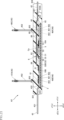
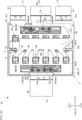
- FIG. 1 is a perspective view of a main portion of a semiconductor device according to a first embodiment of the present disclosure.
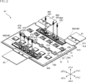
- FIG. 2 is a perspective view of a main part showing the semiconductor device according to the first embodiment of the present disclosure.
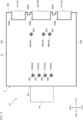
- FIG. 3 is a plan view showing the semiconductor device according to the first embodiment of the present disclosure.
- FIG. 4 is a plan view showing a main part of the semiconductor device according to the first embodiment of the present disclosure.
- FIG. 5 is a side view showing a main part of the semiconductor device according to the first embodiment of the present disclosure.
- FIG. 6 is a plan view showing a main part of the semiconductor device according to the first embodiment of the present disclosure.
- FIG. 7 is a plan view showing a main part of the semiconductor device according to the first embodiment of the present disclosure.
- FIG. 1 is a perspective view of a main portion of a semiconductor device according to a first embodiment of the present disclosure.
- FIG. 2 is a perspective view of a main part showing the semiconductor device according to the first embodiment of
- FIG. 8 is a side view showing the semiconductor device according to the first embodiment of the present disclosure.
- FIG. 9 is a bottom view showing the semiconductor device according to the first embodiment of the present disclosure.
- FIG. 10 is a cross-sectional view taken along line XX in FIG.
- FIG. 11 is a cross-sectional view taken along line XI-XI in FIG.
- FIG. 12 is an enlarged cross-sectional view of a main part showing the semiconductor device according to the first embodiment of the present disclosure.
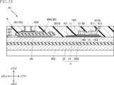
- FIG. 13 is an enlarged cross-sectional view of a main portion showing the semiconductor device according to the first embodiment of the present disclosure.
- FIG. 14 is a cross-sectional view taken along line XIV-XIV in FIG. FIG.
- FIG. 15 is a cross-sectional view taken along line XV-XV in FIG.
- FIG. 16 is a cross-sectional view taken along line XVI-XVI in FIG.
- FIG. 17 is a cross-sectional view taken along line XVII-XVII in FIG.
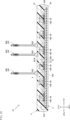
- FIG. 18 is a cross-sectional view taken along line XVIII-XVIII in FIG.
- FIG. 19 is a circuit diagram showing the semiconductor device according to the first embodiment of the present disclosure.
- FIG. 20 is a system configuration diagram showing a vehicle equipped with the semiconductor device according to the first embodiment of the present disclosure.
- FIG. 21 is a cross-sectional view showing a semiconductor device according to the second embodiment of the present disclosure.
- FIG. 22 is a partial plan view showing a semiconductor device according to a third embodiment of the present disclosure.
- an object A is formed on an object B" and “an object A is formed on an object B” include “an object A is formed directly on an object B” and “an object A is formed on an object B with another object interposed between the object A and the object B” unless otherwise specified.
- an object A is disposed on an object B” and “an object A is disposed on an object B” include “an object A is disposed directly on an object B” and “an object A is disposed on an object B with another object interposed between the object A and the object B" unless otherwise specified.
- an object A is located on an object B includes “an object A is located on an object B in contact with an object B” and “an object A is located on an object B with another object interposed between the object A and the object B” unless otherwise specified.
- an object A overlaps an object B when viewed in a certain direction includes “an object A overlaps the entire object B” and “an object A overlaps a part of an object B.”
- a surface A faces in direction B is not limited to the case where the angle of surface A with respect to direction B is 90°, but also includes the case where surface A is tilted with respect to direction B.
- FIGS. 1 to 19 show a semiconductor device according to a first embodiment of the present disclosure.
- the semiconductor device A1 of this embodiment includes a plurality of first semiconductor elements 10A, a plurality of second semiconductor elements 10B, a support substrate 3, a second terminal 42, a third terminal 43, two first terminals 41, a plurality of control terminals 45, a control terminal support 48, a first conductive member 5, a second conductive member 6, and a sealing resin 8.
- FIG. 1 is a perspective view of a main part of the semiconductor device A1.
- FIG. 2 is a perspective view of a main part of the semiconductor device A1.
- FIG. 3 is a plan view of the semiconductor device A1.
- FIG. 4 is a plan view of a main part of the semiconductor device A1.
- FIG. 5 is a side view of a main part of the semiconductor device A1.
- FIG. 6 is a plan view of a main part of the semiconductor device A1.
- FIG. 7 is a plan view of a main part of the semiconductor device A1.
- FIG. 8 is a side view of the semiconductor device A1.
- FIG. 9 is a bottom view of the semiconductor device A1.
- FIG. 10 is a cross-sectional view taken along line X-X in FIG. 4.
- FIG. 10 is a cross-sectional view taken along line X-X in FIG. 4.
- FIG. 11 is a cross-sectional view taken along line XI-XI in FIG. 4.
- FIG. 12 is an enlarged cross-sectional view of a main part of the semiconductor device A1.
- FIG. 13 is an enlarged cross-sectional view of a main part of the semiconductor device A1.
- FIG. 14 is a cross-sectional view taken along line XIV-XIV in FIG. 4.
- FIG. 15 is a cross-sectional view taken along line XV-XV in FIG. 4.
- FIG. 16 is a cross-sectional view taken along line XVI-XVI in FIG. 4.
- FIG. 17 is a cross-sectional view taken along line XVII-XVII in FIG. 4.
- FIG. 18 is a cross-sectional view taken along line XVIII-XVIII in FIG. 4.
- FIG. 19 is a circuit diagram showing semiconductor device A1.
- the thickness direction z is the "thickness direction” of this disclosure
- the first direction x is the “first direction” of this disclosure
- the second direction y is the “second direction” of this disclosure.
- the first semiconductor elements 10A and the second semiconductor elements 10B are electronic components that are the core of the functions of the semiconductor device A1.
- the material of each of the first semiconductor elements 10A and the second semiconductor elements 10B is a semiconductor material mainly made of, for example, SiC (silicon carbide). This semiconductor material is not limited to SiC, and may be Si (silicon), GaN (gallium nitride), or C (diamond).
- Each of the first semiconductor elements 10A and the second semiconductor elements 10B is a power semiconductor chip having a switching function, such as a MOSFET (Metal Oxide Semiconductor Field Effect Transistor).
- MOSFET Metal Oxide Semiconductor Field Effect Transistor
- the first semiconductor elements 10A and the second semiconductor elements 10B are MOSFETs, but are not limited thereto and may be other transistors such as an IGBT (Insulated Gate Bipolar Transistor).
- Each of the first semiconductor elements 10A and the second semiconductor elements 10B is the same element.
- Each of the first semiconductor elements 10A and each of the second semiconductor elements 10B is, for example, an n-channel MOSFET, but may also be a p-channel MOSFET.
- the first semiconductor element 10A and the second semiconductor element 10B each have an element main surface 101 and an element back surface 102.
- the element main surface 101 and the element back surface 102 are separated in the thickness direction z.
- the element main surface 101 faces the z1 side in the thickness direction z
- the element back surface 102 faces the z2 side in the thickness direction z.
- the semiconductor device A1 has four first semiconductor elements 10A and four second semiconductor elements 10B, but the number of first semiconductor elements 10A and the number of second semiconductor elements 10B are not limited to this configuration and are changed as appropriate according to the performance required of the semiconductor device A1.
- four first semiconductor elements 10A and four second semiconductor elements 10B are arranged.
- the number of first semiconductor elements 10A and the number of second semiconductor elements 10B may be two or three, or five or more.
- the number of first semiconductor elements 10A and the number of second semiconductor elements 10B may be equal to or different from each other.
- the number of first semiconductor elements 10A and the number of second semiconductor elements 10B are determined by the current capacity handled by the semiconductor device A1.
- the semiconductor device A1 is configured, for example, as a half-bridge type switching circuit.
- the multiple first semiconductor elements 10A configure the upper arm circuit of the semiconductor device A1
- the multiple second semiconductor elements 10B configure the lower arm circuit.
- the multiple first semiconductor elements 10A are connected in parallel with each other, and in the lower arm circuit, the multiple second semiconductor elements 10B are connected in parallel with each other.
- Each first semiconductor element 10A and each second semiconductor element 10B are connected in series to configure a bridge layer.
- each of the first semiconductor elements 10A is mounted on a first conductive portion 32A of a support substrate 3 described later.
- the first semiconductor elements 10A are arranged, for example, in the second direction y and are spaced apart from each other.
- the first semiconductor elements 10A may be arranged spaced apart from each other in the second direction y and at different positions in the first direction x.
- Each first semiconductor element 10A is conductively bonded to the first conductive portion 32A via a first conductive bonding material 19A.
- the element back surface 102 faces the first conductive portion 32A.
- the first semiconductor elements 10A may be mounted on a metal member different from a part of the DBC substrate or the like.
- the metal member corresponds to the first conductive portion in this disclosure.
- This metal member may be supported by, for example, the first conductive portion 32A.
- each of the second semiconductor elements 10B is mounted on a second conductive portion 32B of the support substrate 3 described later.
- the second semiconductor elements 10B are arranged, for example, in the second direction y and spaced apart from each other.
- the second semiconductor elements 10B may be arranged spaced apart from each other in the second direction y and at different positions in the first direction x.
- Each second semiconductor element 10B is conductively bonded to the second conductive portion 32B via the second conductive bonding material 19B.
- the element back surface 102 faces the second conductive portion 32B.
- the first semiconductor elements 10A and the second semiconductor elements 10B overlap when viewed in the first direction x, but they do not have to overlap.
- the multiple second semiconductor elements 10B may be mounted on a metal member that is different from a part of the DBC substrate, etc.
- the metal member corresponds to the second conductive portion in this disclosure. This metal member may be supported by, for example, the second conductive portion 32B.
- the multiple first semiconductor elements 10A and the multiple second semiconductor elements 10B each have a gate electrode 11, a source electrode 12, a source sense electrode 13, and a drain electrode 15.
- the configurations of the gate electrode 11, the source electrode 12, the source sense electrode 13, and the drain electrode 15 described below are common to each of the first semiconductor elements 10A and each of the second semiconductor elements 10B.
- the gate electrode 11, the source electrode 12, and the source sense electrode 13 are provided on the element main surface 101.
- the gate electrode 11, the source electrode 12, and the source sense electrode 13 are insulated by an insulating film (not shown).
- the drain electrode 15 is provided on the element back surface 102.
- the drain electrode 15 is an example of a first electrode of the present disclosure.
- the drain electrode 15 is the positive electrode of the current path to be switched in the semiconductor device A1.
- the drain electrode 15 covers the entire area (or substantially the entire area) of the back surface 102 of the element.
- the drain electrode 15 is formed, for example, by Ag (silver) plating.
- the source electrode 12 is an example of a second electrode of the present disclosure.
- the source electrode 12 is the negative electrode of the current path to be switched in the semiconductor device A1.
- the gate electrode 11 is an example of a third electrode of the present disclosure.
- the gate electrode 11 is an electrode for switching the conduction state between the drain electrode 15 and the source electrode 12, and a drive signal (for example, a gate voltage) for driving the first semiconductor element 10A (second semiconductor element 10B) is input to the gate electrode 11.
- the source sense electrode 13 is an electrode at the same potential as the source electrode 12.
- each first semiconductor element 10A switches between a conductive state and a cut-off state in response to the drive signal.
- a current flows from the drain electrode 15 to the source electrode 12, and in the cut-off state, this current does not flow.
- each first semiconductor element 10A (each second semiconductor element 10B) performs a switching operation.
- the semiconductor device A1 converts a DC voltage input between the two first terminals 41 and the second terminals 42 into, for example, an AC voltage, using the switching function of the multiple first semiconductor elements 10A and the multiple second semiconductor elements 10B, and outputs the AC voltage from the third terminal 43.
- the support substrate 3 supports a plurality of first semiconductor elements 10A and a plurality of second semiconductor elements 10B.
- the specific configuration of the support substrate 3 is not limited in any way, and may be, for example, a DBC (Direct Bonded Copper) substrate or an AMB (Active Metal Brazing) substrate.
- the support substrate 3 includes an insulating layer 31, a first metal layer 32, and a back metal layer 33.
- the first metal layer 32 includes a first conductive portion 32A and a second conductive portion 32B.
- the dimension of the support substrate 3 in the thickness direction z is, for example, 0.4 mm or more and 3.0 mm or less.
- the insulating layer 31 is, for example, a ceramic with excellent thermal conductivity.
- An example of such a ceramic is SiN (silicon nitride).
- the insulating layer 31 is not limited to ceramics, and may be an insulating resin sheet or the like.
- the insulating layer 31 is, for example, rectangular in plan view.
- the dimension of the insulating layer 31 in the thickness direction z is, for example, 0.05 mm or more and 1.0 mm or less.
- the first conductive portion 32A supports a plurality of first semiconductor elements 10A
- the second conductive portion 32B supports a plurality of second semiconductor elements 10B.
- the first conductive portion 32A and the second conductive portion 32B are formed on the upper surface of the insulating layer 31 (the surface facing the z1 side in the thickness direction z).
- the constituent material of the first conductive portion 32A and the second conductive portion 32B includes, for example, Cu (copper).
- the constituent material may include, for example, Al (aluminum) other than Cu (copper).
- the first conductive portion 32A and the second conductive portion 32B are spaced apart in the first direction x.
- the first conductive portion 32A is located on the x1 side of the second conductive portion 32B in the first direction x.
- the first conductive portion 32A and the second conductive portion 32B are each, for example, rectangular in a plan view.
- the first conductive portion 32A has a first main surface 301A.
- the first main surface 301A is a plane facing the z1 side in the thickness direction z.
- a plurality of first semiconductor elements 10A are respectively bonded to the first main surface 301A of the first conductive portion 32A via a first conductive bonding material 19A.
- the second conductive portion 32B has a second main surface 301B.
- the second main surface 301B is a plane facing the z1 side in the thickness direction z.
- a plurality of second semiconductor elements 10B are bonded to the second main surface 301B of the second conductive portion 32B via a second conductive bonding material 19B.
- the constituent materials of the first conductive bonding material 19A and the second conductive bonding material 19B are not particularly limited, and may be, for example, solder, a metal paste material containing a metal such as Ag (silver), or a sintered metal containing a metal such as Ag (silver).
- the dimension of the first conductive portion 32A and the second conductive portion 32B in the thickness direction z is, for example, 0.1 mm or more and 1.5 mm or less.
- the back metal layer 33 is formed on the lower surface (surface facing the z2 side in the thickness direction z) of the insulating layer 31.
- the constituent material of the back metal layer 33 is the same as the constituent material of the first metal layer 32.
- the back metal layer 33 has a back surface 302.
- the back surface 302 is a flat surface facing the z2 side in the thickness direction z. In the example shown in FIG. 9, the back surface 302 is exposed from the sealing resin 8, for example.
- a heat dissipation member for example, a heat sink
- the back surface 302 may not be exposed from the sealing resin 8 and may be covered by the sealing resin 8.
- the back surface metal layer 33 overlaps both the first conductive portion 32A and the second conductive portion 32B in a plan view.
- the second terminal 42, the third terminal 43, and the two first terminals 41 are each made of a plate-shaped metal plate.
- This metal plate contains, for example, Cu (copper) or a Cu (copper) alloy.
- the DC voltage to be converted is input to the second terminal 42 and the first terminal 41.
- the first terminal 41 is a positive electrode (P terminal), and the second terminal 42 is a negative electrode (N terminal).
- the AC voltage converted by the first semiconductor element 10A and the second semiconductor element 10B is output from the third terminal 43.
- the second terminal 42, the third terminal 43, and the two first terminals 41 each include a portion covered by the sealing resin 8 and a portion exposed from the sealing resin 8.
- the two first terminals 41 are arranged apart from each other in the second direction y, as shown in Figs. 1 to 7.
- the two first terminals 41 are each connected to the first main surface 301A of the first conductive portion 32A.
- the two first terminals 41 are located on the x1 side in the first direction x with respect to the multiple first semiconductor elements 10A, as shown in Figs. 6 and 7.
- the two first terminals 41 are conductive to the first conductive portion 32A, and are conductive to the drain electrodes 15 of each first semiconductor element 10A via the first conductive portion 32A.
- the first terminal 41 has a first terminal portion 411, a first connection portion 412, and a first step portion 413.
- the first terminal portion 411 is exposed from the sealing resin 8 and is used when electrically connecting the semiconductor device A1 to the outside.
- the first connection portion 412 is conductively joined to the first main surface 301A of the first conductive portion 32A.
- the first step portion 413 is interposed between the first terminal portion 411 and the first connection portion 412, and makes the first terminal portion 411 and the first connection portion 412 different in position in the thickness direction z.
- the second terminal 42 is electrically connected to the source electrodes 12 of the second semiconductor elements 10B via the second conductive member 6.
- the second terminal 42 and the second conductive member 6 are formed separately from each other and are electrically connected to each other.
- the second terminal 42 and the second conductive member 6 may be an integral member.
- An integral member is formed, for example, by subjecting a single metal plate material to cutting and bending processes, and does not include a bonding material for bonding the two members to each other.
- the second terminal 42 is located between the two first terminals 41 in the second direction y.
- the second terminal 42 is located on the x1 side of the first direction x with respect to the first semiconductor elements 10A.
- the second terminal 42 has a second terminal portion 421 and a second connection portion 422, as shown in FIG. 14.
- the second terminal portion 421 is exposed from the sealing resin 8 and is a portion used when electrically connecting the semiconductor device A1 to the outside.
- the second terminal portion 421 is located between the two first terminal portions 411 in the second direction y.
- the second terminal portion 421 is exposed from the sealing resin 8.
- the second connection portion 422 extends from the second terminal portion 421 to the x2 side in the x direction.
- the third terminal 43 is conductively joined to the second conductive portion 32B.
- the third terminal 43 is located on the x2 side of the first direction x with respect to the multiple second semiconductor elements 10B.
- the third terminal 43 is conductive to the second conductive portion 32B, and is also conductive to the drain electrodes 15 of the multiple second semiconductor elements 10B via the second conductive portion 32B.
- the number of third terminals 43 is not limited to one, and may be, for example, two or more.
- the third terminal 43 has a third terminal portion 431 and a third connection portion 432.
- the third terminal portion 431 is exposed from the sealing resin 8 and is a portion used when electrically connecting the semiconductor device A1 to the outside.
- the third connection portion 432 extends from the third terminal portion 431 to the x1 side in the x direction.
- the third connection portion 432 is conductively joined to the second main surface 301B of the second conductive portion 32B.
- the multiple control terminals 45 are pin-shaped terminals for controlling each of the first semiconductor elements 10A and each of the second semiconductor elements 10B.
- the multiple control terminals 45 include multiple first control terminals 46A, 46B, 46E and multiple second control terminals 47A, 47B, 47C, 47E.
- the multiple first control terminals 46A, 46B, 46E are used for controlling each of the first semiconductor elements 10A, etc.
- the multiple second control terminals 47A, 47B, 47C, 47E are used for controlling each of the second semiconductor elements 10B, etc.
- the first control terminals 46A, 46B, 46E are arranged apart from each other in the second direction y.
- the first control terminals 46A, 46B, 46E are arranged in a substantially straight line along the second direction y, but this is not limited thereto, and may be arranged at different positions in the first direction.
- each of the first control terminals 46A, 46B, 46E protrudes from the sealing resin 8 to the z1 side in the thickness direction z.
- Each of the first control terminals 46A, 46B, 46E is supported by the first conductive portion 32A via a control terminal support 48 (first support portion 48A described later).
- Each of the first control terminals 46A, 46B, 46E is located between the first semiconductor elements 10A and the second terminal 42 and the first terminal 41 in the first direction x, as shown in FIG. 4 and FIG. 6.
- the first control terminal 46A is a terminal (gate terminal) for inputting a drive signal to the multiple first semiconductor elements 10A.
- a drive signal for driving the multiple first semiconductor elements 10A is input to the first control terminal 46A (for example, a gate voltage is applied).
- the first control terminal 46B is a terminal (source sense terminal) for detecting source signals of the multiple first semiconductor elements 10A.
- the voltage (voltage corresponding to the source current) applied to each source electrode 12 of the multiple first semiconductor elements 10A is detected from the first control terminal 46B.
- the first control terminal 46E is a terminal (drain sense terminal) for detecting the drain signals of the multiple first semiconductor elements 10A.
- the voltage (voltage corresponding to the drain current) applied to the drain electrodes 15 of the multiple first semiconductor elements 10A is detected from the first control terminal 46E.
- the second control terminals 47A, 47B, 47C, and 47E are spaced apart from one another in the second direction y.
- the second control terminals 47A, 47B, 47C, and 47E are arranged in a substantially straight line along the second direction y, but this is not limited thereto, and may be arranged at different positions in the first direction.
- each of the second control terminals 47A, 47B, 47C, and 47E is supported by the second conductive portion 32B via a control terminal support 48 (second support portion 48B described later).
- each of the second control terminals 47A, 47B, 47C, and 47E is located between the second semiconductor elements 10B and the two third terminals 43 in the first direction x.
- the second control terminal 47A is a terminal (gate terminal) for inputting a drive signal to the multiple second semiconductor elements 10B.
- a drive signal for driving the multiple second semiconductor elements 10B is input to the second control terminal 47A (for example, a gate voltage is applied).
- the second control terminal 47B is a terminal (source sense terminal) for detecting source signals of the multiple second semiconductor elements 10B.
- the voltage (voltage corresponding to the source current) applied to each source electrode 12 of the multiple second semiconductor elements 10B is detected from the second control terminal 47B.
- the second control terminals 47C and 47E are terminals used for temperature detection using the thermistor 17.
- Each of the multiple control terminals 45 includes a holder 451 and a metal pin 452.
- the holder 451 is made of a conductive material. As shown in Figures 12 and 13, the holder 451 is bonded to the control terminal support 48 (first metal layer 482 described below) via a conductive bonding material 459.
- the holder 451 includes a cylindrical portion, an upper end flange, and a lower end flange. The upper end flange is connected to the upper part of the cylindrical portion, and the lower end flange is connected to the lower part of the cylindrical portion.
- a metal pin 452 is inserted through at least the upper end flange and the cylindrical portion of the holder 451.
- the holder 451 is covered with sealing resin 8 (second protrusion 852 described below).
- the metal pin 452 is a rod-shaped member extending in the thickness direction z.
- the metal pin 452 is supported, for example, by being pressed into the holder 451.
- the metal pin 452 is electrically connected to the control terminal support 48 (the first metal layer 482 described below) at least via the holder 451.
- the control terminal support 48 supports the multiple control terminals 45.
- the control terminal support 48 is interposed between the first main surface 301A and the second main surface 301B and the multiple control terminals 45 in the thickness direction z.
- the control terminal support 48 includes a first support portion 48A and a second support portion 48B.
- the first support portion 48A is disposed on the first conductive portion 32A and supports the first control terminals 46A to 46E of the control terminals 45.
- the first support portion 48A is bonded to the first conductive portion 32A via a bonding material 49 as shown in FIG. 12.
- the bonding material 49 may be conductive or insulating, and may be, for example, solder.
- the second support portion 48B is disposed on the second conductive portion 32B and supports the second control terminals 47A to 47D of the control terminals 45.
- the second support portion 48B is bonded to the second conductive portion 32B via a bonding material 49 as shown in FIG. 13.
- the control terminal support 48 (each of the first support portion 48A and the second support portion 48B) is formed, for example, from a DBC (Direct Bonded Copper) substrate.
- the control terminal support 48 has an insulating layer 481, a first metal layer 482, and a second metal layer 483 stacked on top of each other.
- the insulating layer 481 is made of, for example, ceramics.
- the insulating layer 481 is, for example, rectangular in plan view.
- the first metal layer 482 is formed on the upper surface of the insulating layer 481, as shown in Figures 12 and 13. Each control terminal 45 is disposed on the first metal layer 482.
- the first metal layer 482 includes, for example, Cu (copper) or a Cu (copper) alloy. As shown in Figures 6 and 7, the first metal layer 482 includes a first portion 482A, a second portion 482B, a fifth portion 482E, a sixth portion 482F, and a seventh portion 482G.
- the first portion 482A, the second portion 482B, the fifth portion 482E, the sixth portion 482F, and the seventh portion 482G are separated and insulated from each other.
- the first portion 482A has multiple wires 71 bonded thereto, and is electrically connected to the gate electrode 11 of each of the first semiconductor elements 10A (each of the second semiconductor elements 10B) via each wire 71. Wires 71, 72, 74, 75, and 76 are omitted in figures other than FIG. 7.
- the first control terminal 46A is bonded to the first portion 482A of the first support portion 48A, and the second control terminal 47A is bonded to 482B of the second support portion 48B.
- the sixth portion 482F is electrically connected to the gate electrode 11 of one of the first semiconductor elements 10A via a wire 71.
- the sixth portion 482F is electrically connected to the first portion 482A via a wire 75.
- the seventh portion 482G has multiple wires 72 bonded thereto, and is electrically connected to the source sense electrodes 13 of the first semiconductor elements 10A (second semiconductor elements 10B) via the wires 72.
- the seventh portion 482G is electrically connected to the second portion 482B via wires 76.
- the first control terminal 46B is bonded to the second portion 482B of the first support portion 48A, and the second control terminal 47B is bonded to the second portion 482B of the second support portion 48B.
- the fifth portion 482E of the first support portion 48A is joined to the wire 74 and is electrically connected to the first conductive portion 32A via the wire 74.
- the first control terminal 46E is joined to the fifth portion 482E of the first support portion 48A.
- the thermistor 17 is conductively joined to the fifth portion 482E and the third portion 482C of the second support portion 48B.
- the second control terminal 47E is joined to the fifth portion 482E of the second support portion 48B, and the second control terminal 47C is joined to the third portion 482C of the second support portion 48B.
- Wires 71, 72, 74, 75, and 76 are, for example, bonding wires.
- the material of each of wires 71, 72, and 74 includes, for example, any of Au (gold), Al (aluminum), and Cu (copper).
- the second metal layer 483 is formed on the lower surface of the insulating layer 481, as shown in Figures 12 and 13.
- the second metal layer 483 of the first support portion 48A is bonded to the first conductive portion 32A via a bonding material 49, as shown in Figure 12.
- the second metal layer 483 of the second support portion 48B is bonded to the second conductive portion 32B via a bonding material 49, as shown in Figure 13.
- the first conductive member 5 and the second conductive member 6 are located on the z1 side in the thickness direction z from the first main surface 301A and the second main surface 301B, and overlap the first main surface 301A and the second main surface 301B in a plan view.
- the first conductive member 5 and the second conductive member 6 are each made of a metal plate material.
- the metal includes, for example, Cu (copper) or a Cu (copper) alloy.
- the first conductive member 5 and the second conductive member 6 are metal plate materials that are appropriately bent.
- the first conductive member 5 is connected to the source electrodes 12 of the multiple first semiconductor elements 10A and the second conductive portion 32B, and provides electrical continuity between the source electrodes 12 of the multiple first semiconductor elements 10A and the second conductive portion 32B.
- the first conductive member 5 forms a path for the main circuit current that is switched by the multiple first semiconductor elements 10A.
- the first conductive member 5 includes a main portion 53, multiple fourth connection portions 51, and multiple fifth connection portions 52.
- the main portion 53 is located between the multiple first semiconductor elements 10A and the second conductive portion 32B in the first direction x, and is a band-shaped portion extending in the second direction y in a planar view.
- the main portion 53 is spaced apart in the thickness direction z from the first main surface 301A and the second main surface 301B on the z1 side of the thickness direction z. As shown in FIG. 14 etc., the main portion 53 is located on the z2 side of the thickness direction z with respect to the main portion 63 of the second conductive member 6 described later.
- the main portion 53 is disposed parallel to the first main surface 301A and the second main surface 301B.
- a plurality of first openings 514 are formed in the main portion 53.
- the plurality of first openings 514 expose portions of the insulating layer 31 located between the first conductive portion 32A and the second conductive portion 32B.
- the plurality of first openings 514 are formed to facilitate the flow of the resin material between the upper side (z1 side in the thickness direction z) and the lower side (z2 side in the thickness direction z) near the main portion 53 (first conductive member 5) when injecting a fluid resin material to form the sealing resin 8.
- the plurality of fourth connection parts 51 and the plurality of fifth connection parts 52 are each connected to the main part 53.
- the plurality of fourth connection parts 51 are arranged corresponding to the plurality of first semiconductor elements 10A.
- each fourth connection part 51 is located on the x1 side of the first direction x with respect to the main part 53.
- Each fifth connection part 52 is located on the x2 side of the first direction x with respect to the main part 53.
- each fourth connection part 51 and the corresponding source electrode 12 of the first semiconductor element 10A are joined via a conductive bonding material 59.
- Each fifth connection part 52 and the second conductive part 32B are joined via a conductive bonding material 59.
- the material of the conductive bonding material 59 is not particularly limited, and may be, for example, solder, a metal paste material, or a sintered metal.
- the fourth connection part 51 has two parts spaced apart in the second direction y. These two parts are joined to the source electrode 12 on either side in the second direction y, sandwiching a gate finger (not shown) of the source electrode 12 of the first semiconductor element 10A.
- the second conductive member 6 is electrically connected to the source electrodes 12 of the second semiconductor elements 10B and the second terminals 42 and 42, and conducts them. As shown in FIG. 1, FIG. 4, and FIG. 18, the second terminals 42 and the second conductive member 6 form a conductive path Cp.
- the conductive path Cp is located outside the first control terminals 46 in the second direction y.
- the second terminals 42 and the second conductive member 6 form two conductive paths Cp.
- One conductive path Cp is located on the y1 side of the second direction y with respect to the first control terminals 46, and the other conductive path Cp is located on the y2 side of the second direction y with respect to the first control terminals 46.
- the two conductive paths Cp are located on both outsides of the first control terminals 46 in the second direction y.
- the conduction path Cp is shown by a dashed line, but this is for ease of understanding, and the actual conduction direction of the conduction path Cp is determined by the shapes of the second terminal 42 and the second conductive member 6, etc.
- the second conductive member 6 has a plurality of sixth connection parts 61, a seventh connection part 62, a main part 63, a plurality of relay parts 64, two relay parts 65, and two relay parts 66, as shown in Figures 4, 13, and 14.
- the sixth connection portions 61 are portions that are individually bonded to the second semiconductor elements 10B. Each sixth connection portion 61 and the source electrode 12 of each second semiconductor element 10B are bonded via a conductive bonding material 69.
- the material of the conductive bonding material 69 is not particularly limited, and may be, for example, solder, a metal paste material, or a sintered metal.
- the sixth connection portion 61 has two flat portions 611 and two first inclined portions 612.
- the two flat portions 611 are aligned in the second direction y.
- the two flat portions 611 are spaced apart from each other in the second direction y.
- the shape of the flat portion 611 is not limited in any way, and in the illustrated example, it is rectangular.
- the two flat portions are joined to the source electrode 12 on both sides in the second direction y, sandwiching a gate finger (not shown) of the source electrode 12 of the second semiconductor element 10B therebetween.
- the two first inclined portions 612 are connected to the x1 side of the two flat portions 611 in the x direction.
- the first inclined portions 612 are inclined so that the further they are from the flat portions 611 in the first direction x, the closer they are to the z1 side in the thickness direction z.
- the two seventh connection parts 62 are each electrically connected to the second connection part 422 of the second terminal 42.
- the seventh connection part 62 is conductively joined to the second connection part 422.
- the method of conductive joining There are no limitations on the method of conductive joining, and methods such as ultrasonic joining, laser joining, welding, or methods using solder, metal paste, sintered silver, etc. may be used as appropriate.
- the seventh connection part 62 is joined to the second connection part 422 via a conductive joining material 69.
- the two seventh connection parts 62 are arranged apart in the second direction y.
- the main portion 63 is interposed between the sixth connection portions 61 and the seventh connection portion 62.
- the main portion 63 is a flat portion perpendicular to the thickness direction z.
- the multiple relay parts 64 are individually interposed between the multiple sixth connection parts 61 and the main part 63.
- the multiple relay parts 64 are arranged radially from the main part 63 toward the multiple sixth connection parts 61.
- the two relay portions 65 extend outward in the second direction y from the two seventh connection portions 62. As shown in Figures 4, 10, and 15, the relay portions 65 overlap the first connection portion 412 of the first terminal 41 when viewed in the thickness direction z. The relay portions 65 are located on the z1 side of the first connection portion 412 in the thickness direction z.
- the two relay parts 66 are individually interposed between the main part 63 and the two relay parts 65.
- the two relay parts 66 are located on both outer sides in the second direction y relative to the multiple first control terminals 46.
- the relay part 66 has an extension part 661.
- the extension part 661 is a part that extends to the z2 side in the thickness direction z on the outer side in the second direction y.
- the sealing resin 8 covers the first semiconductor elements 10A, the second semiconductor elements 10B, the support substrate 3 (excluding the back surface 302), the second terminal 42, the third terminal 43, and a portion of each of the two first terminals 41, the control terminals 45, the control terminal support 48, the first conductive member 5, the second conductive member 6, and the wires 71, 72, and 74.
- the sealing resin 8 is made of, for example, a black epoxy resin.
- the sealing resin 8 is formed, for example, by molding.
- the sealing resin 8 has, for example, a dimension in the first direction x of about 35 mm to 60 mm, a dimension in the second direction y of about 35 mm to 50 mm, and a dimension in the thickness direction z of about 4 mm to 15 mm. These dimensions are the size of the maximum portion along each direction.
- the sealing resin 8 has a resin main surface 81, a resin back surface 82, and a plurality of resin side surfaces 831 to 834.
- the resin main surface 81 and the resin back surface 82 are separated in the thickness direction z, as shown in Figures 8, 10, 16, etc.
- the resin main surface 81 faces the z1 side in the thickness direction z
- the resin back surface 82 faces the z2 side in the thickness direction z.
- a plurality of control terminals 45 protrude from the resin main surface 81.
- the resin back surface 82 is frame-shaped in plan view surrounding the back surface 302 (the lower surface of the back surface metal layer 33) of the support substrate 3.
- the back surface 302 of the support substrate 3 is exposed from the resin back surface 82, and is, for example, flush with the resin back surface 82.
- the multiple resin side surfaces 831 to 834 are each connected to both the resin main surface 81 and the resin back surface 82, and are sandwiched between them in the thickness direction z. As shown in FIG. 3 and other figures, the resin side surface 831 and the resin side surface 832 are separated in the first direction x. The resin side surface 831 faces the x2 side of the first direction x, and the resin side surface 832 faces the x1 side of the first direction x. Two third terminals 43 protrude from the resin side surface 831, and the second terminal 42, the second terminal 42, and the first terminal 41 protrude from the resin side surface 832. As shown in FIG. 3 and other figures, the resin side surface 833 and the resin side surface 834 are separated in the second direction y. The resin side surface 833 faces the y2 side of the second direction y, and the resin side surface 834 faces the y1 side of the second direction y.
- a plurality of recesses 832a are formed on the resin side surface 832.
- Each recess 832a is a portion recessed in the first direction x in a plan view.
- the plurality of recesses 832a are formed between the second terminal 42 and the first terminal 41 in a plan view.
- the plurality of recesses 832a are provided to increase the creepage distance along the resin side surface 832 between the second terminal 42 and the first terminal 41.
- a plurality of recesses 832b are formed on the resin side surface 832.
- the plurality of recesses 832b are recessed from the resin side surface 832 toward the x2 side in the first direction x.
- the first terminal portions 411 of the two first terminals 41 and the second terminal portions 421 of the second terminals 42 are exposed from the plurality of recesses 832b.
- the resin side surface 832 may not be formed with a plurality of recesses 832b, and the first terminal portions 411 and the second connection portions 422 may be configured to protrude from the resin side surface 832 toward the x1 side in the first direction x, for example.
- the sealing resin 8 has a plurality of second protrusions 852.
- the plurality of second protrusions 852 protrude from the resin main surface 81 in the thickness direction z.
- the plurality of second protrusions 852 overlap the plurality of control terminals 45 in a plan view.
- Each metal pin 452 of the plurality of control terminals 45 protrudes from each second protrusion 852.
- Each second protrusion 852 is frustum-shaped.
- the second protrusion 852 covers the holder 451 and a portion of the metal pin 452 in each control terminal 45.
- the vehicle B1 is, for example, an electric vehicle (EV).
- EV electric vehicle
- vehicle B1 is equipped with an on-board charger 91, a storage battery 92, and a drive system 93.
- Power is supplied to the on-board charger 91 wirelessly from a power supply facility (not shown) installed outdoors. Alternatively, power may be supplied from the power supply facility to the on-board charger 91 via a wired connection.
- the on-board charger 91 is configured with a step-up DC-DC converter. The voltage of the power supplied to the on-board charger 91 is stepped up by the converter and then supplied to the storage battery 92. The stepped-up voltage is, for example, 600V.
- the drive system 93 drives the vehicle B1.
- the drive system 93 has an inverter 931 and a drive source 932.
- the semiconductor device A1 constitutes part of the inverter 931.
- the power stored in the storage battery 92 is supplied to the inverter 931.
- the power supplied from the storage battery 92 to the inverter 931 is DC power.
- a step-up DC-DC converter may be further provided between the storage battery 92 and the inverter 931.
- the inverter 931 converts DC power into AC power.
- the inverter 931 including the semiconductor device A1 is conductive to the drive source 932.
- the driving source 932 has an AC motor and a transmission.
- the AC motor rotates and the rotation is transmitted to the transmission.
- the transmission appropriately reduces the rotation speed transmitted from the AC motor and then rotates the drive shaft of the vehicle B1. This drives the vehicle B1.
- the semiconductor device A1 in the inverter 931 is necessary to output AC power whose frequency has been appropriately changed to correspond to the required rotation speed of the AC motor.
- the conductive path Cp formed by the second conductive member 6 and the second terminal 42 is disposed outside the first control terminals 46 in the second direction y. This makes it possible to more appropriately dispose the second terminal 42 and the first control terminals 46 while avoiding interference between the second conductive member 6 and the second terminal 42 and the first control terminals 46.
- the second conductive member 6 and the second terminal 42 are configured as separate components. This makes it possible to prevent the individual components that make up the conductive path Cp from becoming excessively large.
- two conductive paths Cp are configured.
- the two conductive paths Cp are arranged on both outsides of the multiple first control terminals 46 in the second direction y, and are paths that bypass the multiple first control terminals 46 to the outside in the second direction y. This makes it possible to allow a larger current to flow between the second terminal 42 and the second conductive member 6 while avoiding interference between the second conductive member 6 and the multiple first control terminals 46 and the second terminal 42.
- the relay portion 65 overlaps with the first connection portion 412 when viewed in the thickness direction z, and is located on the z1 side of the first connection portion 412 in the thickness direction z. This makes it possible to more reliably insulate the first terminal 41 from the second conductive member 6 while preventing the semiconductor device A1 from becoming larger in size when viewed in the thickness direction z.
- the sixth connection portion 61 has two flat portions 611 and two first inclined portions 612.
- the two first inclined portions 612 are connected to the x1 side of the two flat portions 611 in the first direction x. This makes it possible to prevent the current flowing through the source electrode 12 from concentrating in one place.
- the two flat portions 611 are spaced apart in the second direction y. This allows current to flow reliably through both the two flat portions 611 and the two first inclined portions 612, which is advantageous in preventing current concentration.
- the gate finger (not shown) of the source electrode 12 can be positioned between them.
- FIGS. 21 and 22 show other embodiments of the present disclosure.
- elements that are the same as or similar to those in the above embodiment are given the same reference numerals as in the above embodiment.
- the configurations of the various parts in each embodiment can be combined with each other as appropriate to the extent that no technical contradictions arise.
- FIG. 21 shows a semiconductor device according to a second embodiment of the present disclosure.
- the semiconductor device A2 of this embodiment differs from the above-described embodiment in the configuration of the second conductive member 6 and the second terminal 42.
- the second conductive member 6 and the second terminal 42 are configured as a single member. In other words, the second conductive member 6 and the second terminal 42 are connected to each other without a joint or the like that joins them together.
- the second terminal 42 and the multiple first control terminals 46 can be more appropriately arranged.
- the specific configuration of the second conductive member 6 and the second terminal 42 that constitute the conductive path Cp is not limited in any way.
- the configuration in which the second conductive member 6 and the second terminal 42 are electrically connected is not limited to the configuration in which the second conductive member 6 and the second terminal 42 are conductively joined as in the semiconductor device A1, but is a concept that includes a configuration in which the second conductive member 6 and the second terminal 42 are formed by an integrated member as in this embodiment.
- FIG. 22 shows a semiconductor device according to a third embodiment of the present disclosure.
- the semiconductor device A3 of this embodiment differs from the above-described embodiments in the number of conductive paths Cp.
- one conductive path Cp is formed by the second terminal 42 and the second conductive member 6.
- the conductive path Cp is located on the y1 side of the second direction y with respect to the multiple first control terminals 46.
- the second conductive member 6 has one seventh connection portion 62, one relay portion 65, and one relay portion 66.
- This embodiment also allows the second terminal 42 and the multiple first control terminals 46 to be more appropriately arranged. As can be understood from this embodiment, there is no limitation on the number of conductive paths Cp.
- the semiconductor device and vehicle according to the present disclosure are not limited to the above-mentioned embodiment.
- the specific configuration of each part of the semiconductor device and vehicle according to the present disclosure can be freely designed in various ways.
- the present disclosure includes the embodiments described in the following appendix.
- Appendix 1 A first conductive portion; A second conductive portion; one or more first semiconductor elements having a first electrode which is a positive electrode of a current path to be switched, a second electrode which is a negative electrode, and a third electrode for switching a conduction state between the first electrode and the second electrode; one or more second semiconductor elements having a first electrode which is a positive electrode of a current path to be switched, a second electrode which is a negative electrode, and a third electrode for switching a conduction state between the first electrode and the second electrode; Two first terminals; A second terminal; A third terminal; A first conductive member; A second conductive member; A plurality of first control terminals; A plurality of second control terminals; and a sealing resin; the first conductive portion has a first main surface facing a first side in a thickness direction; the second conductive portion has a second main surface facing the first side in the thickness direction, In a first direction perpendicular to the thickness direction, the first conductive portion is disposed on a first side, and the second
- Appendix 2 The semiconductor device according to claim 1, wherein the first terminal has a first terminal portion exposed from the sealing resin and a first connection portion conductively joined to the first main surface. Appendix 3. 3. The semiconductor device according to claim 2, wherein the second terminal has a second terminal portion exposed from the sealing resin. Appendix 4. 4. The semiconductor device according to claim 3, wherein the third terminal has a third terminal portion exposed from the sealing resin and a third connection portion conductively joined to the second main surface. Appendix 5. The semiconductor device according to claim 3 or 4, wherein the first conductive member has a fourth connection portion conductively joined to the second electrode of the first semiconductor element and a fifth connection portion conductively joined to the second main surface. Appendix 6.
- the semiconductor device according to claim 5 wherein the first conductive member has a plurality of the fourth connection portions that are individually conductively joined to the second electrodes of the plurality of the first semiconductor elements. Appendix 7. 7. The semiconductor device according to claim 6, wherein the first conductive member further has a main portion interposed between the plurality of fourth connection portions and the fifth connection portion. Appendix 8. 8. The semiconductor device according to claim 3, further comprising a first support portion interposed between the plurality of first control terminals and the first conductive portion. Appendix 9. 9. The semiconductor device according to claim 3, wherein the second terminal and the second conductive member are separate from each other and are conductively joined. Appendix 10.
- the second terminal has a second connection portion extending from the second terminal portion to the second side in the first direction, 10.
- Appendix 11 The semiconductor device according to claim 10, wherein the second conductive member has a sixth connection portion that is conductively joined to the second electrode of the second semiconductor element.
- Appendix 12. a plurality of the second semiconductor elements arranged apart from each other in the second direction; The semiconductor device according to claim 11, wherein the second conductive member has a plurality of the sixth connection portions that are individually conductively joined to the second electrodes of the plurality of the second semiconductor elements.
- Appendix 13. 13 13.
- the second conductive member further includes a seventh connection portion conductively joined to the second connection portion, and a main portion interposed between the sixth connection portion and the seventh connection portion.
- Appendix 14. 14 The semiconductor device according to claim 13, wherein the second terminal and the second conductive member form two of the conductive paths located on both outer sides of the plurality of first control terminals in the second direction. Appendix 15. 15. The semiconductor device according to claim 14, wherein the second conductive member has two of the seventh connection portions and a plurality of relay portions that individually relay the main portion and the two seventh connection portions. Appendix 16. 9. The semiconductor device according to claim 3, wherein the second terminal and the second conductive member are an integral member. Appendix 17. A driving source; A semiconductor device according to any one of claims 1 to 16, The semiconductor device is electrically connected to the drive source.
Landscapes
- Lead Frames For Integrated Circuits (AREA)
Abstract
半導体装置(A1)は、第1導電部(32A)と、第2導電部(32B)と、第1半導体素子(10A)と、第2半導体素子(10B)と、2つの第1端子(41)と、第2端子(42)と、第3端子(43)と、第1導通部材(5)と、第2導通部材(6)と、複数の第1制御端子(46)と、複数の第2制御端子(47)と、封止樹脂とを備える。厚さ方向(z)と直交する第1方向(x)において、前記第1導電部および前記第2導電部は、互いに離隔配置されている。前記第2端子と前記第2導通部材とによって、前記厚さ方向および前記第1方向に直交する第2方向(y)における前記複数の第1制御端子の外側に位置する導通経路(Cp)が構成されている。
Description
本開示は、半導体装置および車両に関する。
従来、MOSFET(Metal Oxide Semiconductor Field Effect Transistor)やIGBT(Insulated Gate Bipolar Transistor)などの電力用スイッチング素子を備える半導体装置が知られている。特許文献1には、従来の半導体装置(パワーモジュール)が開示されている。特許文献1に記載の半導体装置は、スイッチング対象である主電流が流れる入力端子および出力端子と、複数の制御端子とを備える。
入力端子および出力端子と、複数の制御端子とは、適切に配置されることが好ましい。
本開示は、従来より改良が施された半導体装置を提供することを一の課題とする。特に本開示は、上記した事情に鑑み、端子をより適切に配置することが可能な半導体装置を提供することを一の課題とする。また本開示は、そのような半導体装置を備えた車両を提供することを一の課題とする。
本開示の第1の側面によって提供される半導体装置は、第1導電部と、第2導電部と、スイッチング対象の電流経路の正極である第1電極、負極である第2電極、および前記第1電極と前記第2電極との導通状態を切り替えるための第3電極を有する1以上の第1半導体素子と、スイッチング対象の電流経路の正極である第1電極、負極である第2電極、および前記第1電極と前記第2電極との導通状態を切り替えるための第3電極を有する1以上の第2半導体素子と、2つの第1端子と、第2端子と、第3端子と、第1導通部材と、第2導通部材と、複数の第1制御端子と、複数の第2制御端子と、封止樹脂と、を備える。前記第1導電部は、厚さ方向の第1側を向く第1主面を有し、前記第2導電部は、前記厚さ方向の前記第1側を向く第2主面を有する。前記厚さ方向と直交する第1方向において、前記第1導電部は、第1側に配置され、前記第2導電部は、第2側に配置されている。前記第1半導体素子の前記第1電極は、前記第1主面に導通接合されており、前記第2半導体素子の前記第1電極は、前記第2主面に導通接合されている。前記複数の第1制御端子は、前記第1方向において前記第1半導体素子に対して前記第1側に位置し、前記第1方向および厚さ方向と直交する第2方向に互いに離隔して配置されており、且つ前記第1導電部に対して前記厚さ方向の第1側に突出している。前記2つの第1端子は、前記第2方向において互いに離れて配置され、各々が前記第1主面に接続されており、且つ前記複数の第1制御端子よりも前記第1方向の前記第1側に突出している。前記第2端子は、前記第2方向において前記2つの第1端子の間に位置し、且つ前記複数の第1制御端子よりも前記第1方向の前記第1側に突出している。前記第3端子は、前記第2主面に接続されている。前記第1導通部材は、前記第1半導体素子の前記第2電極と前記第2主面とに導通接合されている。前記第2導通部材は、前記第2半導体素子の前記第2電極と前記第2端子とに電気的に接続されている。前記第2端子と前記第2導通部材とによって、前記第2方向における前記複数の第1制御端子の外側に位置する導通経路が構成されている。
本開示の第2の側面によって提供される車両は、駆動源と、本開示の第1の側面によって提供される半導体装置と、を備え、前記半導体装置は、前記駆動源に導通している。
上記構成によれば、半導体装置において、端子をより適切に配置することができる。
本開示のその他の特徴および利点は、添付図面を参照して以下に行う詳細な説明によって、より明らかとなろう。
以下、本開示の好ましい実施の形態につき、図面を参照して具体的に説明する。
本開示における「第1」、「第2」、「第3」等の用語は、単に識別のために用いたものであり、それらの対象物に順列を付することを意図していない。
本開示において、「ある物Aがある物Bに形成されている」および「ある物Aがある物B上に形成されている」とは、特段の断りのない限り、「ある物Aがある物Bに直接形成されていること」、および、「ある物Aとある物Bとの間に他の物を介在させつつ、ある物Aがある物Bに形成されていること」を含む。同様に、「ある物Aがある物Bに配置されている」および「ある物Aがある物B上に配置されている」とは、特段の断りのない限り、「ある物Aがある物Bに直接配置されていること」、および、「ある物Aとある物Bとの間に他の物を介在させつつ、ある物Aがある物Bに配置されていること」を含む。同様に、「ある物Aがある物B上に位置している」とは、特段の断りのない限り、「ある物Aがある物Bに接して、ある物Aがある物B上に位置していること」、および、「ある物Aとある物Bとの間に他の物が介在しつつ、ある物Aがある物B上に位置していること」を含む。「ある物Aがある物Bにある方向に見て重なる」とは、特段の断りのない限り、「ある物Aがある物Bのすべてに重なること」、および、「ある物Aがある物Bの一部に重なること」を含む。本開示において「ある面Aが方向B(の一方側または他方側)を向く」とは、面Aの方向Bに対する角度が90°である場合に限定されず、面Aが方向Bに対して傾いている場合を含む。
図1~図19は、本開示の第1実施形態に係る半導体装置を示している。本実施形態の半導体装置A1は、複数の第1半導体素子10A、複数の第2半導体素子10B、支持基板3、第2端子42、第3端子43、2つの第1端子41、複数の制御端子45、制御端子支持体48、第1導通部材5、第2導通部材6および封止樹脂8を備えている。
図1は、半導体装置A1を示す要部斜視図である。図2は、半導体装置A1を示す要部斜視図である。図3は、半導体装置A1を示す平面図である。図4は、半導体装置A1を示す要部平面図である。図5は、半導体装置A1を示す要部側面図である。図6は、半導体装置A1を示す要部平面図である。図7は、半導体装置A1を示す要部平面図である。図8は、半導体装置A1を示す側面図である。図9は、半導体装置A1を示す底面図である。図10は、図4のX-X線に沿う断面図である。図11は、図4のXI-XI線に沿う断面図である。図12は、半導体装置A1を示す要部拡大断面図である。図13は、半導体装置A1を示す要部拡大断面図である。図14は、図4のXIV-XIV線に沿う断面図である。図15は、図4のXV-XV線に沿う断面図である。図16は、図4のXVI-XVI線に沿う断面図である。図17は、図4のXVII-XVII線に沿う断面図である。図18は、図4のXVIII-XVIII線に沿う断面図である。図19は、半導体装置A1を示す回路図である。
これらの図において、たとえば、厚さ方向zは、本開示の「厚さ方向」であり、第1方向xは、本開示の「第1方向」であり、第2方向yは、本開示の「第2方向」である。
複数の第1半導体素子10Aおよび複数の第2半導体素子10Bはそれぞれ、半導体装置A1の機能中枢となる電子部品である。各第1半導体素子10Aおよび各第2半導体素子10Bの構成材料は、たとえばSiC(炭化ケイ素)を主とする半導体材料である。この半導体材料は、SiCに限定されず、Si(シリコン)、GaN(窒化ガリウム)あるいはC(ダイヤモンド)などであってもよい。各第1半導体素子10Aおよび各第2半導体素子10Bは、たとえば、MOSFET(Metal Oxide Semiconductor Field Effect Transistor)などのスイッチング機能を有するパワー半導体チップである。本実施形態においては、第1半導体素子10Aおよび第2半導体素子10BがMOSFETである場合を示すが、これに限定されず、IGBT(Insulated Gate Bipolar Transistor;絶縁ゲートバイポーラトランジスタ)などの他のトランジスタであってもよい。各第1半導体素子10Aおよび各第2半導体素子10Bは、いずれも同一素子である。各第1半導体素子10Aおよび各第2半導体素子10Bは、たとえばnチャネル型のMOSFETであるが、pチャネル型のMOSFETであってもよい。
第1半導体素子10Aおよび第2半導体素子10Bはそれぞれ、図7,図12、図13に示すように、素子主面101および素子裏面102を有する。各第1半導体素子10Aおよび各第2半導体素子10Bにおいて、素子主面101と素子裏面102とは厚さ方向zに離隔する。素子主面101は、厚さ方向zのz1側を向き、素子裏面102は、厚さ方向zのz2側を向く。
本実施形態では、半導体装置A1は、4つの第1半導体素子10Aと4つの第2半導体素子10Bとを備えているが、第1半導体素子10Aの数および第2半導体素子10Bの数は、本構成に限定されず、半導体装置A1に要求される性能に応じて適宜変更される。図6、図7の例では、第1半導体素子10Aおよび第2半導体素子10Bがそれぞれ4個ずつ配置される。第1半導体素子10Aおよび第2半導体素子10Bの数は、それぞれ2個または3個でもよく、それぞれ5個以上でもよい。第1半導体素子10Aの数と第2半導体素子10Bの数とは、等しくてもよく、異なってもよい。第1半導体素子10Aおよび第2半導体素子10Bの数は、半導体装置A1が取り扱う電流容量によって決定される。
半導体装置A1は、図19に示すように、たとえばハーフブリッジ型のスイッチング回路として構成される。この場合、複数の第1半導体素子10Aは、半導体装置A1の上アーム回路を構成し、複数の第2半導体素子10Bは、下アーム回路を構成する。上アーム回路において、複数の第1半導体素子10Aは互いに並列に接続され、下アーム回路において、複数の第2半導体素子10Bは互いに並列に接続される。各第1半導体素子10Aと各第2半導体素子10Bとは、直列に接続され、ブリッジ層を構成する。
複数の第1半導体素子10Aはそれぞれ、図6、図7および図17などに示すように、後述の支持基板3の第1導電部32Aに搭載されている。図6、図7に示す例では、複数の第1半導体素子10Aは、たとえば第2方向yに並んでおり、互いに離隔している。複数の第1半導体素子10Aは、第2方向yに互いに離隔した配置であって、第1方向xにおける位置が互いに異なる配置であってもよい。各第1半導体素子10Aは、第1導電性接合材19Aを介して、第1導電部32Aに導通接合されている。各第1半導体素子10Aは、第1導電部32Aに接合された際、素子裏面102が第1導電部32Aに対向する。本実施形態とは異なり、複数の第1半導体素子10Aは、DBC基板等の一部とは異なる金属部材に搭載されていてもよい。この場合、当該金属部材が本開示における第1導電部に相当する。この金属部材は、たとえば第1導電部32Aに支持されていてもよい。
複数の第2半導体素子10Bはそれぞれ、図6、図7および図16などに示すように、後述の支持基板3の第2導電部32Bに搭載されている。図6、図7に示す例では、複数の第2半導体素子10Bは、たとえば第2方向yに並んでおり、互いに離隔している。複数の第2半導体素子10Bは、第2方向yに互いに離隔した配置であって、第1方向xにおける位置が互いに異なる配置であってもよい。各第2半導体素子10Bは、第2導電性接合材19Bを介して、第2導電部32Bに導通接合されている。各第2半導体素子10Bは、第2導電部32Bに接合された際、素子裏面102が第2導電部32Bに対向する。図7から理解されるように、第1方向xに視て、複数の第1半導体素子10Aと複数の第2半導体素子10Bとは、重なっているが、重なっていなくてもよい。本実施形態とは異なり、複数の第2半導体素子10Bは、DBC基板等の一部とは異なる金属部材に搭載されていてもよい。この場合、当該金属部材が本開示における第2導電部に相当する。この金属部材は、たとえば第2導電部32Bに支持されていてもよい。
複数の第1半導体素子10Aおよび複数の第2半導体素子10Bはそれぞれ、ゲート電極11、ソース電極12、ソースセンス電極13およびドレイン電極15を有する。以下で説明するゲート電極11、ソース電極12、ソースセンス電極13およびドレイン電極15の構成は、各第1半導体素子10Aおよび各第2半導体素子10Bにおいて共通する。ゲート電極11、ソース電極12およびソースセンス電極13は、素子主面101に設けられている。ゲート電極11、ソース電極12およびソースセンス電極13は、図示しない絶縁膜により絶縁されている。ドレイン電極15は、素子裏面102に設けられている。
ドレイン電極15は、本開示の第1電極の一例である。ドレイン電極15は、半導体装置A1のスイッチング対象の電流経路の正極である。ドレイン電極15は、素子裏面102の全域(あるいは略全域)を覆っている。ドレイン電極15は、たとえばAg(銀)めっきにより構成される。ソース電極12は、本開示の第2電極の一例である。ソース電極12は、半導体装置A1のスイッチング対象の電流経路の負極である。ゲート電極11は、本開示の第3電極の一例である。ゲート電極11は、ドレイン電極15とソース電極12との導通状態を切り替えるための電極であり、第1半導体素子10A(第2半導体素子10B)を駆動させるための駆動信号(たとえばゲート電圧)が入力される。ソースセンス電極13は、ソース電極12と同電位の電極である。
各第1半導体素子10A(各第2半導体素子10B)は、ゲート電極11に駆動信号(ゲート電圧)が入力されると、この駆動信号に応じて、導通状態と遮断状態とが切り替わる。導通状態では、ドレイン電極15からソース電極12に電流が流れ、遮断状態では、この電流が流れない。つまり、各第1半導体素子10A(各第2半導体素子10B)は、スイッチング動作を行う。半導体装置A1は、複数の第1半導体素子10Aおよび複数の第2半導体素子10Bのスイッチング機能により、2つの第1端子41と第2端子42との間に入力される直流電圧をたとえば交流電圧に変換して、第3端子43から交流電圧を出力する。
支持基板3は、複数の第1半導体素子10Aおよび複数の第2半導体素子10Bを支持する。支持基板3の具体的構成は何ら限定されず、たとえばDBC(Direct Bonded Copper)基板またはAMB(Active Metal Brazing)基板で構成される。支持基板3は、絶縁層31、第1金属層32および裏面金属層33を含む。第1金属層32は、第1導電部32Aおよび第2導電部32Bを含む。支持基板3の厚さ方向zの寸法は、たとえば0.4mm以上3.0mm以下である。
絶縁層31は、たとえば熱伝導性の優れたセラミックスである。このようなセラミックスとしては、たとえばSiN(窒化ケイ素)がある。絶縁層31は、セラミックスに限定されず、絶縁樹脂シートなどであってもよい。絶縁層31は、たとえば平面視矩形状である。絶縁層31の厚さ方向zの寸法は、たとえば0.05mm以上1.0mm以下である。
第1導電部32Aは、複数の第1半導体素子10Aを支持し、第2導電部32Bは、複数の第2半導体素子10Bを支持する。第1導電部32Aおよび第2導電部32Bは、絶縁層31の上面(厚さ方向zのz1側を向く面)に形成されている。第1導電部32Aおよび第2導電部32Bの構成材料は、たとえばCu(銅)を含む。当該構成材料はCu(銅)以外のたとえばAl(アルミニウム)を含んでいてもよい。第1導電部32Aおよび第2導電部32Bは、第1方向xに離隔する。第1導電部32Aは、第2導電部32Bの第1方向xのx1側に位置する。第1導電部32Aおよび第2導電部32Bはそれぞれ、たとえば平面視矩形状である。第1導電部32Aおよび第2導電部32Bは、第1導通部材5および第2導通部材6とともに、複数の第1半導体素子10Aおよび複数の第2半導体素子10Bによってスイッチングされる主回路電流の経路を構成する。
第1導電部32Aは、第1主面301Aを有する。第1主面301Aは、厚さ方向zのz1側を向く平面である。第1導電部32Aの第1主面301Aには、第1導電性接合材19Aを介して複数の第1半導体素子10Aがそれぞれ接合されている。第2導電部32Bは、第2主面301Bを有する。第2主面301Bは、厚さ方向zのz1側を向く平面である。第2導電部32Bの第2主面301Bには、第2導電性接合材19Bを介して複数の第2半導体素子10Bが接合されている。第1導電性接合材19Aおよび第2導電性接合材19Bの構成材料は特に限定されず、たとえば、はんだ、Ag(銀)等の金属を含む金属ペースト材、あるいは、Ag(銀)等の金属を含む焼結金属などである。第1導電部32Aおよび第2導電部32Bの厚さ方向zの寸法は、たとえば0.1mm以上1.5mm以下である。
裏面金属層33は、絶縁層31の下面(厚さ方向zのz2側を向く面)に形成されている。裏面金属層33の構成材料は、第1金属層32の構成材料と同じである。裏面金属層33は、裏面302を有する。裏面302は、厚さ方向zのz2側を向く平面である。裏面302は、図9に示す例では、たとえば封止樹脂8から露出する。裏面302には、図示しない放熱部材(たとえばヒートシンク)などが取り付け可能である。裏面302は、封止樹脂8から露出せず、封止樹脂8に覆われていてもよい。裏面金属層33は、平面視において、第1導電部32Aおよび第2導電部32Bの双方に重なる。
第2端子42、第3端子43、および2つの第1端子41はそれぞれ、板状の金属板からなる。この金属板は、たとえばCu(銅)またはCu(銅)合金を含む。
図19に示すように、第2端子42および第1端子41には、電力変換対象となる直流電圧が入力される。第1端子41は正極(P端子)であり、第2端子42はそれぞれ負極(N端子)である。第3端子43から、第1半導体素子10Aおよび第2半導体素子10Bにより電力変換された交流電圧が出力される。第2端子42、第3端子43、および2つの第1端子41はそれぞれ、封止樹脂8に覆われた部分と封止樹脂8から露出した部分とを含む。
2つの第1端子41は、図1~図7に示すように、第2方向yにおいて互いに離れて配置されている。2つの第1端子41は、各々が第1導電部32Aの第1主面301Aに接続されている。2つの第1端子41は、図6、図7などに示すように、複数の第1半導体素子10Aに対して、第1方向xのx1側に位置する。2つの第1端子41は、第1導電部32Aに導通し、かつ、第1導電部32Aを介して、各第1半導体素子10Aのドレイン電極15に導通する。本実施形態においては、第1端子41は、第1端子部411、第1接続部412および第1段差部413を有する。
第1端子部411は、封止樹脂8から露出しており、半導体装置A1を電気的に外部接続する際に用いられる部位である。第1接続部412は、図10および図15に示すように、第1導電部32Aの第1主面301Aに導通接合されている。導通接合の手法は何ら限定されず、超音波接合、レーザ接合、溶接等の手法、あるいははんだ、金属ペースト、銀焼結体等を用いた手法、等が適宜採用される。第1段差部413は、第1端子部411と第1接続部412との間に介在しており、第1端子部411と第1接続部412との厚さ方向zにおける位置を異ならせている。
第2端子42は、第2導通部材6を介して複数の第2半導体素子10Bのソース電極12に導通している。本実施形態においては、第2端子42と第2導通部材6とは、互いに別体に形成されており、互いに導通接合されている。第2端子42と第2導通部材6とは、一体の部材であってもよい。一体の部材とは、たとえば単一の金属板材料に対して切断加工および折り曲げ加工等を施すことによって形成されており、互いを接合するための接合材等を含まない構成をいう。図1および図4に示すように、第2端子42は、第2方向yにおいて2つの第1端子41の間に位置する。第2端子42は、複数の第1半導体素子10Aに対して、第1方向xのx1側に位置する。本実施形態においては、第2端子42は、図14に示すように、第2端子部421および第2接続部422を有する。
第2端子部421は、封止樹脂8から露出しており、半導体装置A1を電気的に外部接続する際に用いられる部位である。第2端子部421は、第2方向yにおいて2つの第1端子部411の間に位置する。第2端子部421は、封止樹脂8から露出している。第2接続部422は、第2端子部421からx方向のx2側に延びている。
第3端子43は、図6、図7および図14から理解されるように、第2導電部32Bに導通接合されている。導通接合の手法は何ら限定されず、超音波接合、レーザ接合、溶接等の手法、あるいははんだ、金属ペースト、銀焼結体等を用いた手法、等が適宜採用される。第3端子43は、図6などに示すように、複数の第2半導体素子10Bに対して、第1方向xのx2側に位置する。第3端子43は、第2導電部32Bに導通し、かつ、第2導電部32Bを介して、複数の第2半導体素子10Bのドレイン電極15に導通する。第3端子43の数は、1つに限定されず、たとえば2以上であってもよい。
本実施形態においては、第3端子43は、第3端子部431および第3接続部432を有する。第3端子部431は、封止樹脂8から露出しており、半導体装置A1を電気的に外部接続する際に用いられる部位である。第3接続部432は、第3端子部431からx方向のx1側に延びている。第3接続部432は、第2導電部32Bの第2主面301Bに導通接合されている。
複数の制御端子45は、各第1半導体素子10Aおよび各第2半導体素子10Bを制御するためのピン状の端子である。複数の制御端子45は、複数の第1制御端子46A,46B,46Eおよび複数の第2制御端子47A,47B,47C,47Eを含む。複数の第1制御端子46A,46B,46Eは、各第1半導体素子10Aの制御などに用いられる。複数の第2制御端子47A,47B,47C,47Eは、各第2半導体素子10Bの制御などに用いられる。
複数の第1制御端子46A,46B,46Eは、第2方向yに互いに離隔して配置されている。図示された例においては、複数の第1制御端子46A,46B,46Eは、第2方向yに沿ってほぼ一直線上に配置されているが、これに限定されず、たとえば第1方向における位置が互いに異なる配置であってもよい。各第1制御端子46A,46B,46Eは、図6、図11および図18などに示すように、封止樹脂8から厚さ方向zのz1側に突出している。各第1制御端子46A,46B,46Eは、制御端子支持体48(後述の第1支持部48A)を介して、第1導電部32Aに支持される。各第1制御端子46A,46B,46Eは、図4および図6に示すように、第1方向xにおいて、複数の第1半導体素子10Aと、第2端子42および第1端子41との間に位置する。
第1制御端子46Aは、複数の第1半導体素子10Aの駆動信号入力用の端子(ゲート端子)である。第1制御端子46Aには、複数の第1半導体素子10Aを駆動させるための駆動信号が入力される(たとえばゲート電圧が印加される)。
第1制御端子46Bは、複数の第1半導体素子10Aのソース信号検出用の端子(ソースセンス端子)である。第1制御端子46Bから、複数の第1半導体素子10Aの各ソース電極12に印加される電圧(ソース電流に対応した電圧)が検出される。
第1制御端子46Eは、複数の第1半導体素子10Aのドレイン信号検出用の端子(ドレインセンス端子)である。第1制御端子46Eから、複数の第1半導体素子10Aのドレイン電極15に印加される電圧(ドレイン電流に対応した電圧)が検出される。
複数の第2制御端子47A,47B,47C,47Eは、第2方向yに互いに離隔して配置されている。図示された例においては、複数の第2制御端子47A,47B,47C,47Eは、第2方向yに沿ってほぼ一直線上に配置されているが、これに限定されず、たとえば第1方向における位置が互いに異なる配置であってもよい。各第2制御端子47A,47B,47C,47Eは、図6および図11などに示すように、制御端子支持体48(後述の第2支持部48B)を介して、第2導電部32Bに支持される。各第2制御端子47A,47B,47C,47Eは、図4および図6に示すように、第1方向xにおいて、複数の第2半導体素子10Bと2つの第3端子43との間に位置する。
第2制御端子47Aは、複数の第2半導体素子10Bの駆動信号入力用の端子(ゲート端子)である。第2制御端子47Aには、複数の第2半導体素子10Bを駆動させるための駆動信号が入力される(たとえばゲート電圧が印加される)。
第2制御端子47Bは、複数の第2半導体素子10Bのソース信号検出用の端子(ソースセンス端子)である。第2制御端子47Bから、複数の第2半導体素子10Bの各ソース電極12に印加される電圧(ソース電流に対応した電圧)が検出される。
第2制御端子47C,47Eは、サーミスタ17を用いた温度検出に用いられる端子である。
複数の制御端子45(複数の第1制御端子46A~46Eおよび複数の第2制御端子47A~47D)はそれぞれ、ホルダ451および金属ピン452を含む。
ホルダ451は、導電性材料からなる。ホルダ451は、図12、図13に示すように、導電性接合材459を介して、制御端子支持体48(後述の第1金属層482)に接合されている。ホルダ451は、筒状部、上端鍔部および下端鍔部を含む。上端鍔部は、筒状部の上方につながり、下端鍔部は、筒状部の下方につながる。ホルダ451のうちの少なくとも上端鍔部および筒状部に、金属ピン452が挿通されている。ホルダ451は、封止樹脂8(後述の第2突出部852)に覆われている。
金属ピン452は、厚さ方向zに延びる棒状部材である。金属ピン452は、たとえばホルダ451に圧入されることで支持されている。金属ピン452は、少なくともホルダ451を介して、制御端子支持体48(後述の第1金属層482)に導通する。
制御端子支持体48は、複数の制御端子45を支持する。制御端子支持体48は、厚さ方向zにおいて、第1主面301Aおよび第2主面301Bと複数の制御端子45との間に介在する。
制御端子支持体48は、第1支持部48Aおよび第2支持部48Bを含む。第1支持部48Aは、第1導電部32A上に配置され、複数の制御端子45のうちの複数の第1制御端子46A~46Eを支持する。第1支持部48Aは、図12に示すように、接合材49を介して、第1導電部32Aに接合されている。接合材49は、導電性でも絶縁性でもよいが、たとえばはんだが用いられる。第2支持部48Bは、第2導電部32B上に配置され、複数の制御端子45のうちの複数の第2制御端子47A~47Dを支持する。第2支持部48Bは、図13に示すように、接合材49を介して、第2導電部32Bに接合されている。
制御端子支持体48(第1支持部48Aおよび第2支持部48Bのそれぞれ)は、たとえばDBC(Direct Bonded Copper)基板で構成される。制御端子支持体48は、互いに積層された絶縁層481、第1金属層482および第2金属層483を有する。
絶縁層481は、たとえばセラミックスからなる。絶縁層481は、たとえば平面視矩形状である。
第1金属層482は、図12、図13などに示すように、絶縁層481の上面に形成されている。各制御端子45は、第1金属層482上に配置されている。第1金属層482は、たとえばCu(銅)またはCu(銅)合金を含む。図6および図7などに示すように、第1金属層482は、第1部分482A、第2部分482B、第5部分482E、第6部分482F、第7部分482Gを含む。第1部分482A、第2部分482B、第5部分482E、第6部分482F、第7部分482G互いに離隔し、絶縁されている。
第1部分482Aは、複数のワイヤ71が接合され、各ワイヤ71を介して、各第1半導体素子10A(各第2半導体素子10B)のゲート電極11に導通する。図7以外の図においては、ワイヤ71,72,74,75,76を省略している。第1支持部48Aの第1部分482Aには、第1制御端子46Aが接合されており、第2支持部48Bの482Bには、第2制御端子47Aが接合されている。
第6部分482Fは、ワイヤ71を介して1つの第1半導体素子10Aのゲート電極11と導通している。第6部分482Fは、ワイヤ75を介して第1部分482Aと導通している。
第7部分482Gは、複数のワイヤ72が接合され、各ワイヤ72を介して、各第1半導体素子10A(各第2半導体素子10B)のソースセンス電極13に導通する。第7部分482Gは、ワイヤ76を介して第2部分482Bと導通している。第1支持部48Aの第2部分482Bには、第1制御端子46Bが接合されており、第2支持部48Bの第2部分482Bには、第2制御端子47Bが接合されている。
図6に示すように、第1支持部48Aの第5部分482Eは、ワイヤ74が接合され、ワイヤ74を介して、第1導電部32Aに導通する。第1支持部48Aの第5部分482Eには、第1制御端子46Eが接合されている。
第2支持部48Bの第5部分482Eと第3部分482Cには、サーミスタ17が導通接合されている。第2支持部48Bの第5部分482Eには、第2制御端子47Eが接合されており、第2支持部48Bの第3部分482Cには、第2制御端子47Cが接合されている。
ワイヤ71,72,74,75,76は、たとえばボンディングワイヤである。各ワイヤ71,72,74の構成材料は、たとえばAu(金)、Al(アルミ)あるいはCu(銅)のいずれかを含む。
第2金属層483は、図12、図13などに示すように、絶縁層481の下面に形成されている。第1支持部48Aの第2金属層483は、図12に示すように、接合材49を介して、第1導電部32Aに接合される。第2支持部48Bの第2金属層483は、図13に示すように、接合材49を介して、第2導電部32Bに接合される。
第1導通部材5および第2導通部材6は、第1導電部32Aおよび第2導電部32Bとともに、複数の第1半導体素子10Aおよび複数の第2半導体素子10Bによってスイッチングされる主回路電流の経路を構成する。第1導通部材5および第2導通部材6は、第1主面301Aおよび第2主面301Bから厚さ方向zのz1側に位置し、かつ、平面視において第1主面301Aおよび第2主面301Bに重なる。本実施形態では、第1導通部材5および第2導通部材6はそれぞれ、金属製の板材により構成される。当該金属は、たとえばCu(銅)またはCu(銅)合金を含む。具体的には、第1導通部材5および第2導通部材6は、適宜折り曲げられた金属製の板材である。
図2および図6に示すように、第1導通部材5は、複数の第1半導体素子10Aのソース電極12と第2導電部32Bとに接続され、複数の第1半導体素子10Aのソース電極12と第2導電部32Bとを導通させる。第1導通部材5は、複数の第1半導体素子10Aによってスイッチングされる主回路電流の経路を構成する。第1導通部材5は、図2および図6に示すように、主部53、複数の第4接続部51および複数の第5接続部52を含む。
主部53は、第1方向xにおいて、複数の第1半導体素子10Aと第2導電部32Bとの間に位置し、平面視において第2方向yに延びる帯状の部位である。主部53は、厚さ方向zにおいて第1主面301Aおよび第2主面301Bから厚さ方向zのz1側に離隔している。図14などに示すように、主部53は、後述する第2導通部材6の主部63に対して厚さ方向zのz2側に位置する。
本実施形態において、主部53は、第1主面301Aおよび第2主面301Bと平行に配置されている。主部53には、複数の第1開口514が形成されている。複数の第1開口514からは、絶縁層31のうち第1導電部32Aと第2導電部32Bとの間に位置する部分が現れている。複数の第1開口514は、封止樹脂8を形成するために流動性の樹脂材料を注入する際に、主部53(第1導通部材5)の付近において上側(厚さ方向zのz1側)と下側(厚さ方向zのz2側)との間で樹脂材料を流動しやすくするために形成される。
図6などに示すように、複数の第4接続部51および複数の第5接続部52はそれぞれ、主部53につながっている。複数の第4接続部51は、複数の第1半導体素子10Aに対応して配置される。具体的には、各第4接続部51は、主部53に対して第1方向xのx1側に位置している。各第5接続部52は、主部53に対して第1方向xのx2側に位置している。図12に示すように、各第4接続部51とこれに対応する第1半導体素子10Aのソース電極12とは、導電性接合材59を介して接合される。各第5接続部52と第2導電部32Bとは、導電性接合材59を介して接合される。導電性接合材59の構成材料は特に限定されず、たとえばはんだ、金属ペースト材、あるいは、焼結金属などである。本実施形態においては、第4接続部51は、第2方向yに離隔した2つの部分を有する。これらの2つの部分は、第1半導体素子10Aのソース電極12のゲートフィンガー(図示略)を挟んで、第2方向yの両側においてソース電極12に接合されている。
第2導通部材6は、複数の第2半導体素子10Bのソース電極12と第2端子42および第2端子42とに電気的に接続されており、これらを導通させている。図1、図4および図18に示すように、第2端子42と第2導通部材6とによって、導通経路Cpが構成されている。導通経路Cpは、複数の第1制御端子46に対して第2方向yの外側に位置している。本実施形態においては、第2端子42と第2導通部材6とによって、2つの導通経路Cpが構成されている。1つの導通経路Cpは、複数の第1制御端子46に対して第2方向yのy1側に位置しており、もう1つの導通経路Cpは、複数の第1制御端子46に対して第2方向yのy2側に位置している。すなわち、2つの導通経路Cpは、複数の第1制御端子46に対して第2方向yの両外側に位置している。図示された例においては、導通経路Cpは、一点鎖線で示しているが、これは理解の便宜であり、実際の導通経路Cpの導通方向は、第2端子42および第2導通部材6の形状等によって決定される。
本実施形態においては、第2導通部材6は、図4、図13および図14に示すように、複数の第6接続部61、第7接続部62、主部63複数の中継部64、2つの中継部65および2つの中継部66を有する。
複数の第6接続部61は、複数の第2半導体素子10Bに個別に接合される部位である。各第6接続部61と各第2半導体素子10Bのソース電極12とは、導電性接合材69を介して接合される。導電性接合材69の構成材料は特に限定されず、たとえばはんだ、金属ペースト材、あるいは、焼結金属などである。本実施形態において、第6接続部61は、2つの平坦部611および2つの第1傾斜部612を有する。
2つの平坦部611は、第2方向yに並んでいる。2つの平坦部611は、第2方向yに互いに離隔している。平坦部611の形状は何ら限定されず、図示された例においては、矩形状である。2つの平坦部は、第2半導体素子10Bのソース電極12のゲートフィンガー(図示略)を挟んで、第2方向yの両側においてソース電極12に接合されている。
2つの第1傾斜部612は、2つの平坦部611のx方向のx1側に繋がる。第1傾斜部612は、第1方向xにおいて平坦部611から離隔するほど厚さ方向zのz1側に位置するように傾斜している。
2つの第7接続部62は、第2端子42の第2接続部422にそれぞれ電気的に接続されている。図示された例においては、第7接続部62は、第2接続部422に導通接合されている。導通接合の手法は何ら限定されず、超音波接合、レーザ接合、溶接等の手法、あるいははんだ、金属ペースト、銀焼結体等を用いた手法、等が適宜採用される。図示された例においては、第7接続部62は、導電性接合材69を介して第2接続部422に接合されている。2つの第7接続部62は、第2方向yに離れて配置されている。
主部63は、複数の第6接続部61と第7接続部62との間に介在している。主部63は、厚さ方向zに対して直交する平板状の部位である。
複数の中継部64は、複数の第6接続部61と主部63との間に個別に介在している。図示された例においては、複数の中継部64は、主部63から複数の第6接続部61に向けて放射状に配置されている。
2つの中継部65は、2つの第7接続部62から第2方向yの外側に延びている。図4、図10および図15に示すように、中継部65は、厚さ方向zに視て、第1端子41の第1接続部412と重なる。中継部65は、第1接続部412に対して厚さ方向zのz1側に位置している。
2つの中継部66は、主部63と2つの中継部65との間に個別に介在している。2つの中継部66は、複数の第1制御端子46に対して第2方向yの両外側に位置している。図示された例においては、中継部66は、延出部661を有する。延出部661は、第2方向yの外側において厚さ方向zのz2側に延出する部分である。
封止樹脂8は、複数の第1半導体素子10Aと、複数の第2半導体素子10Bと、支持基板3(裏面302を除く)と、第2端子42、第3端子43、および2つの第1端子41の一部ずつと、複数の制御端子45の一部ずつと、制御端子支持体48と、第1導通部材5と、第2導通部材6と、複数のワイヤ71,72,74と、をそれぞれ覆っている。封止樹脂8は、たとえば黒色のエポキシ樹脂で構成される。封止樹脂8は、たとえばモールド成形により形成される。封止樹脂8は、たとえば第1方向xの寸法が35mm~60mm程度であり、たとえば第2方向yの寸法が35mm~50mm程度であり、たとえば厚さ方向zの寸法が4mm~15mm程度である。これらの寸法は、各方向に沿う最大部分の大きさである。封止樹脂8は、樹脂主面81、樹脂裏面82および複数の樹脂側面831~834を有する。
樹脂主面81と樹脂裏面82とは、図8、図10および図16などに示すように、厚さ方向zに離隔する。樹脂主面81は、厚さ方向zのz1側を向き、樹脂裏面82は、厚さ方向zのz2側を向く。樹脂主面81から複数の制御端子45(複数の第1制御端子46A~46Eおよび複数の第2制御端子47A~47D)が突き出ている。樹脂裏面82は、図9に示すように、平面視において支持基板3の裏面302(裏面金属層33の下面)を囲む枠状である。支持基板3の裏面302は、樹脂裏面82から露出し、たとえば樹脂裏面82と面一である。
複数の樹脂側面831~834はそれぞれ、樹脂主面81および樹脂裏面82の双方につながり、かつ、厚さ方向zにおいてこれらに挟まれている。図3などに示すように、樹脂側面831と樹脂側面832とは第1方向xに離隔する。樹脂側面831は第1方向xのx2側を向き、樹脂側面832は、第1方向xのx1側を向く。樹脂側面831から2つの第3端子43が突き出ており、樹脂側面832から第2端子42、第2端子42および第1端子41が突き出ている。図3などに示すように、樹脂側面833と樹脂側面834とは、第2方向yに離隔する。樹脂側面833は、第2方向yのy2側を向き、樹脂側面834は、第2方向yのy1側を向く。
樹脂側面832には、図3に示すように、複数の凹部832aが形成されている。各凹部832aは、平面視において第1方向xに窪んだ部位である。複数の凹部832aは、平面視において第2端子42と第1端子41との間に形成されている。複数の凹部832aは、第2端子42と第1端子41との樹脂側面832に沿う沿面距離を大きくするために設けられている。
樹脂側面832には、図3、図9~図11、図14および図15に示すように、複数の凹部832bが形成されている。複数の凹部832bは、樹脂側面832から第1方向xのx2側に凹んでいる。複数の凹部832bからは、2つの第1端子41の第1端子部411と第2端子42の第2端子部421とが露出している。樹脂側面832に複数の凹部832bが形成されておらず、第1端子部411および第2接続部422は、たとえば樹脂側面832から第1方向xのx1側に突出する構成であってもよい。
封止樹脂8は、図11および図18に示すように、複数の第2突出部852を有する。複数の第2突出部852は、樹脂主面81から厚さ方向zに突出している。複数の第2突出部852は、平面視において複数の制御端子45に重なる。複数の制御端子45の各金属ピン452は、各第2突出部852から突き出ている。各第2突出部852は、円錐台状である。第2突出部852は、各制御端子45において、ホルダ451と金属ピン452の一部とを覆う。
次に、図20に基づき、半導体装置A1が搭載された車両B1について説明する。車両B1は、たとえば電気自動車(EV)である。
図20に示すように、車両B1は、車載充電器91、蓄電池92および駆動系統93を備える。車載充電器91には、屋外に設置された給電施設(図示略)から無線により電力が供給される。この他、給電施設から車載充電器91への電力の供給手段は、有線でもよい。車載充電器91には、昇圧型のDC-DCコンバータが構成されている。車載充電器91に供給された電力の電圧は、当該コンバータにより昇圧された後、蓄電池92に給電される。昇圧された電圧は、たとえば600Vである。
駆動系統93は、車両B1を駆動する。駆動系統93は、インバータ931および駆動源932を有する。半導体装置A1は、インバータ931の一部を構成する。蓄電池92に蓄えられた電力は、インバータ931に給電される。蓄電池92からインバータ931に給電される電力は、直流電力である。この他、図20に示す電力系統とは異なり、蓄電池92とインバータ931との間に昇圧型のDC-DCコンバータをさらに設けてもよい。インバータ931は、直流電力を交流電力に変換する。半導体装置A1を含めたインバータ931は、駆動源932に導通している。
駆動源932は、交流モータおよび変速機を有する。インバータ931によって変換された交流電力が駆動源932に供給されると、交流モータが回転するとともに、その回転が変速機に伝達される。変速機は、交流モータから伝達された回転数を適宜減じた上で、車両B1の駆動軸を回転させる。これにより、車両B1が駆動する。車両B1の駆動にあたっては、アクセルペダルの変動量などの情報に基づき交流モータの回転数を自在に操作する必要がある。インバータ931における半導体装置A1は、要求される交流モータの回転数に対応させるべく、周波数が適宜変化された交流電力を出力するために必要である。
次に、本実施形態の作用について説明する。
図1、図4および図18に示すように、第2導通部材6および第2端子42によって構成された導通経路Cpが、第2方向yにおいて複数の第1制御端子46の外側に配置されている。このため、第2導通部材6および第2端子42と複数の第1制御端子46とが干渉することを回避しつつ、第2端子42、および複数の第1制御端子46をより適切に配置することができる。
第2導通部材6と第2端子42とは、別体の部品として構成されている。これにより、導通経路Cpを構成する個々の部品が、過度に大きくなることを回避することができる。
半導体装置A1においては、2つの導通経路Cpが構成されている。2つの導通経路Cpは、複数の第1制御端子46の第2方向yの両外側に配置されており、複数の第1制御端子46を第2方向yの外側に迂回する経路となっている。これにより、第2導通部材6および第2端子42と複数の第1制御端子46とが干渉することを回避しつつ、第2端子42と第2導通部材6とにより多くの電流を流すことができる。
図4、図10および図15に示すように、中継部65は、厚さ方向zに視て第1接続部412と重なり、厚さ方向zにおいて第1接続部412のz1側に位置している。これにより、第1端子41と第2導通部材6とをより確実に絶縁しつつ、半導体装置A1の厚さ方向zに視た大きさが大きくなることを抑制することができる。
第6接続部61は、2つの平坦部611と2つの第1傾斜部612とを有する。2つの第1傾斜部612は、2つの平坦部611に対して第1方向xのx1側に繋がっている。これにより、ソース電極12に流れる電流が一箇所に集中することを抑制することができる。
2つの平坦部611は、第2方向yに離隔している。これにより、2つの平坦部611および2つの第1傾斜部612の双方に、確実に電流を流すことが可能であり、電流集中の抑制に好ましい。
2つの平坦部611を互いに離隔することにより、これらの間にソース電極12のゲートフィンガー(図示略)を配置させることができる。
図21、図22は、本開示の他の実施形態を示している。同図において、上記実施形態と同一または類似の要素には、上記実施形態と同一の符号を付している。各実施形態における各部の構成は、技術的な矛盾を生じない範囲において相互に適宜組み合わせ可能である。
図21は、本開示の第2実施形態に係る半導体装置を示している。本実施形態の半導体装置A2は、第2導通部材6および第2端子42の構成が、上述した実施形態と異なっている。
本実施形態においては、第2導通部材6と第2端子42とは、一体の部材によって構成されている。すなわち、第2導通部材6と第2端子42とは、互いを接合する接合部等を介することなく、繋がっている。
本実施形態によっても、第2端子42、および複数の第1制御端子46をより適切に配置することができる。本実施形態から理解されるように、導通経路Cpを構成する第2導通部材6および第2端子42の具体的な構成は、何ら限定されない。第2導通部材6と第2端子42とが電気的に接続された構成とは、半導体装置A1のように第2導通部材6と第2端子42とが導通接合された構成に限定されず、本実施形態のように第2導通部材6と第2端子42とが一体の部材によって形成された構成を含む概念である。
図22は、本開示の第3実施形態に係る半導体装置を示している。本実施形態の半導体装置A3は、導通経路Cpの個数が、上述した実施形態と異なっている。
本実施形態においては、第2端子42および第2導通部材6によって、1つの導通経路Cpが構成されている。本実施形態の導通経路Cpは、複数の第1制御端子46に対して第2方向yのy1側に位置している。第2導通部材6は、1つの第7接続部62、1つの中継部65および1つの中継部66を有する。
本実施形態によっても、第2端子42、および複数の第1制御端子46をより適切に配置することができる。本実施形態から理解されるように、導通経路Cpの個数は、何ら限定されない。
本開示に係る半導体装置および車両は、上述した実施形態に限定されるものではない。本開示に係る半導体装置および車両の各部の具体的な構成は、種々に設計変更自在である。本開示は、以下の付記に記載された実施形態を含む。
付記1.
第1導電部と、
第2導電部と、
スイッチング対象の電流経路の正極である第1電極、負極である第2電極、および前記第1電極と前記第2電極との導通状態を切り替えるための第3電極を有する1以上の第1半導体素子と、
スイッチング対象の電流経路の正極である第1電極、負極である第2電極、および前記第1電極と前記第2電極との導通状態を切り替えるための第3電極を有する1以上の第2半導体素子と、
2つの第1端子と、
第2端子と、
第3端子と、
第1導通部材と、
第2導通部材と、
複数の第1制御端子と、
複数の第2制御端子と、
封止樹脂と、を備え、
前記第1導電部は、厚さ方向の第1側を向く第1主面を有し、
前記第2導電部は、前記厚さ方向の前記第1側を向く第2主面を有し、
前記厚さ方向と直交する第1方向において、前記第1導電部は、第1側に配置され、前記第2導電部は、第2側に配置され、
前記第1半導体素子の前記第1電極は、前記第1主面に導通接合されており、
前記第2半導体素子の前記第1電極は、前記第2主面に導通接合されており、
前記複数の第1制御端子は、前記第1方向において前記第1半導体素子に対して前記第1側に位置し、前記第1方向および厚さ方向と直交する第2方向に互いに離隔して配置されており、且つ前記第1導電部に対して前記厚さ方向の第1側に突出しており、
前記2つの第1端子は、前記第2方向において互いに離れて配置され、各々が前記第1主面に接続されており、且つ前記複数の第1制御端子よりも前記第1方向の前記第1側に突出しており、
前記第2端子は、前記第2方向において前記2つの第1端子の間に位置し、且つ前記複数の第1制御端子よりも前記第1方向の前記第1側に突出しており、
前記第3端子は、前記第2主面に接続されており、
前記第1導通部材は、前記第1半導体素子の前記第2電極と前記第2主面とに導通接合されており、
前記第2導通部材は、前記第2半導体素子の前記第2電極と前記第2端子とに電気的に接続されており、
前記第2端子と前記第2導通部材とによって、前記第2方向における前記複数の第1制御端子の外側に位置する導通経路が構成されている、半導体装置。
付記2.
前記第1端子は、前記封止樹脂から露出する第1端子部と、前記第1主面に導通接合された第1接続部と、を有する、付記1に記載の半導体装置。
付記3.
前記第2端子は、前記封止樹脂から露出する第2端子部を有する、付記2に記載の半導体装置。
付記4.
前記第3端子は、前記封止樹脂から露出する第3端子部および前記第2主面に導通接合された第3接続部を有する、付記3に記載の半導体装置。
付記5.
前記第1導通部材は、前記第1半導体素子の前記第2電極に導通接合された第4接続部と、前記第2主面に導通接合された第5接続部と、を有する、付記3または4に記載の半導体装置。
付記6.
前記第2方向に互いに離隔して配置された複数の前記第1半導体素子を備え、
前記第1導通部材は、前記複数の前記第1半導体素子の前記第2電極に個別に導通接合された複数の前記第4接続部を有する、付記5に記載の半導体装置。
付記7.
前記第1導通部材は、前記複数の第4接続部と前記第5接続部との間に介在する主部をさらに有する、付記6に記載の半導体装置。
付記8.
前記複数の第1制御端子と前記第1導電部との間に介在する第1支持部をさらに備える、付記3ないし7のいずれかに記載の半導体装置。
付記9.
前記第2端子と前記第2導通部材とは、互いに別体であり、且つ導通接合されている、付記3ないし8のいずれかに記載の半導体装置。
付記10.
前記第2端子は、前記第2端子部から前記第1方向の前記第2側に延びる第2接続部を有し、
前記第2接続部と前記第2導通部材とが導通接合されている、付記9に記載の半導体装置。
付記11.
前記第2導通部材は、前記第2半導体素子の前記第2電極に導通接合された第6接続部を有する、付記10に記載の半導体装置。
付記12.
前記第2方向に互いに離隔して配置された複数の前記第2半導体素子を備え、
前記第2導通部材は、前記複数の前記第2半導体素子の前記第2電極に個別に導通接合された複数の前記第6接続部を有する、付記11に記載の半導体装置。
付記13.
前記第2導通部材は、前記第2接続部に導通接合された第7接続部と、前記第6接続部および前記第7接続部の間に介在する主部と、をさらに有する、付記12に記載の半導体装置。
付記14.
前記第2端子と前記第2導通部材とによって、前記第2方向における前記複数の第1制御端子の両外側に位置する2つの前記導通経路が構成されている、付記13に記載の半導体装置。
付記15.
前記第2導通部材は、2つの前記第7接続部と、前記主部と前記2つの第7接続部とを個別に中継する複数の中継部と、を有する、付記14に記載の半導体装置。
付記16.
前記第2端子と前記第2導通部材とは、一体の部材である、付記3ないし8のいずれかに記載の半導体装置。
付記17.
駆動源と、
付記1ないし16のいずれかに記載の半導体装置と、を備え、
前記半導体装置は、前記駆動源に導通している、車両。
第1導電部と、
第2導電部と、
スイッチング対象の電流経路の正極である第1電極、負極である第2電極、および前記第1電極と前記第2電極との導通状態を切り替えるための第3電極を有する1以上の第1半導体素子と、
スイッチング対象の電流経路の正極である第1電極、負極である第2電極、および前記第1電極と前記第2電極との導通状態を切り替えるための第3電極を有する1以上の第2半導体素子と、
2つの第1端子と、
第2端子と、
第3端子と、
第1導通部材と、
第2導通部材と、
複数の第1制御端子と、
複数の第2制御端子と、
封止樹脂と、を備え、
前記第1導電部は、厚さ方向の第1側を向く第1主面を有し、
前記第2導電部は、前記厚さ方向の前記第1側を向く第2主面を有し、
前記厚さ方向と直交する第1方向において、前記第1導電部は、第1側に配置され、前記第2導電部は、第2側に配置され、
前記第1半導体素子の前記第1電極は、前記第1主面に導通接合されており、
前記第2半導体素子の前記第1電極は、前記第2主面に導通接合されており、
前記複数の第1制御端子は、前記第1方向において前記第1半導体素子に対して前記第1側に位置し、前記第1方向および厚さ方向と直交する第2方向に互いに離隔して配置されており、且つ前記第1導電部に対して前記厚さ方向の第1側に突出しており、
前記2つの第1端子は、前記第2方向において互いに離れて配置され、各々が前記第1主面に接続されており、且つ前記複数の第1制御端子よりも前記第1方向の前記第1側に突出しており、
前記第2端子は、前記第2方向において前記2つの第1端子の間に位置し、且つ前記複数の第1制御端子よりも前記第1方向の前記第1側に突出しており、
前記第3端子は、前記第2主面に接続されており、
前記第1導通部材は、前記第1半導体素子の前記第2電極と前記第2主面とに導通接合されており、
前記第2導通部材は、前記第2半導体素子の前記第2電極と前記第2端子とに電気的に接続されており、
前記第2端子と前記第2導通部材とによって、前記第2方向における前記複数の第1制御端子の外側に位置する導通経路が構成されている、半導体装置。
付記2.
前記第1端子は、前記封止樹脂から露出する第1端子部と、前記第1主面に導通接合された第1接続部と、を有する、付記1に記載の半導体装置。
付記3.
前記第2端子は、前記封止樹脂から露出する第2端子部を有する、付記2に記載の半導体装置。
付記4.
前記第3端子は、前記封止樹脂から露出する第3端子部および前記第2主面に導通接合された第3接続部を有する、付記3に記載の半導体装置。
付記5.
前記第1導通部材は、前記第1半導体素子の前記第2電極に導通接合された第4接続部と、前記第2主面に導通接合された第5接続部と、を有する、付記3または4に記載の半導体装置。
付記6.
前記第2方向に互いに離隔して配置された複数の前記第1半導体素子を備え、
前記第1導通部材は、前記複数の前記第1半導体素子の前記第2電極に個別に導通接合された複数の前記第4接続部を有する、付記5に記載の半導体装置。
付記7.
前記第1導通部材は、前記複数の第4接続部と前記第5接続部との間に介在する主部をさらに有する、付記6に記載の半導体装置。
付記8.
前記複数の第1制御端子と前記第1導電部との間に介在する第1支持部をさらに備える、付記3ないし7のいずれかに記載の半導体装置。
付記9.
前記第2端子と前記第2導通部材とは、互いに別体であり、且つ導通接合されている、付記3ないし8のいずれかに記載の半導体装置。
付記10.
前記第2端子は、前記第2端子部から前記第1方向の前記第2側に延びる第2接続部を有し、
前記第2接続部と前記第2導通部材とが導通接合されている、付記9に記載の半導体装置。
付記11.
前記第2導通部材は、前記第2半導体素子の前記第2電極に導通接合された第6接続部を有する、付記10に記載の半導体装置。
付記12.
前記第2方向に互いに離隔して配置された複数の前記第2半導体素子を備え、
前記第2導通部材は、前記複数の前記第2半導体素子の前記第2電極に個別に導通接合された複数の前記第6接続部を有する、付記11に記載の半導体装置。
付記13.
前記第2導通部材は、前記第2接続部に導通接合された第7接続部と、前記第6接続部および前記第7接続部の間に介在する主部と、をさらに有する、付記12に記載の半導体装置。
付記14.
前記第2端子と前記第2導通部材とによって、前記第2方向における前記複数の第1制御端子の両外側に位置する2つの前記導通経路が構成されている、付記13に記載の半導体装置。
付記15.
前記第2導通部材は、2つの前記第7接続部と、前記主部と前記2つの第7接続部とを個別に中継する複数の中継部と、を有する、付記14に記載の半導体装置。
付記16.
前記第2端子と前記第2導通部材とは、一体の部材である、付記3ないし8のいずれかに記載の半導体装置。
付記17.
駆動源と、
付記1ないし16のいずれかに記載の半導体装置と、を備え、
前記半導体装置は、前記駆動源に導通している、車両。
A1,A2:半導体装置 B1:車両
3:支持基板 5:第1導通部材
6:第2導通部材 8:封止樹脂
10A:第1半導体素子 10B:第2半導体素子
11:ゲート電極 12:ソース電極
13:ソースセンス電極 15:ドレイン電極
19A:第1導電性接合材 19B:第2導電性接合材
31:絶縁層 32:第1金属層
32A:第1導電部 32B:第2導電部
33:裏面金属層 41:第1端子
42:第2端子 43:第3端子 45:制御端子
46,46A,46B,46C,46D,46E:第1制御端子
47A,47B,47C,47D,47E:第2制御端子
48:制御端子支持体 48A:第1支持部
48B:第2支持部 49:接合材
51:第4接続部 52:第5接続部
53:主部 59:導電性接合材
61:第6接続部 62:第7接続部
63:主部 64:段差部
66:第3経路部 69:導電性接合材
71,72,74:ワイヤ 81:樹脂主面
82:樹脂裏面 91:車載充電器
92:蓄電池 93:駆動系統
101:素子主面 102:素子裏面
301A:第1主面 301B:第2主面
302:裏面 411:第1端子部
412:第1接続部 413:第1段差部
421:第2端子部 422:第2接続部
431:第3端子部 432:第3接続部
451:ホルダ 452:金属ピン
459:導電性接合材 481:絶縁層
482:第1金属層 482A:第1部分
482B:第2部分 482C:第3部分
482E:第5部分 483:第2金属層
514:第1開口 602:第1段差部
603:第2段差部 611:平坦部
612:第1傾斜部 831:樹脂側面
832:樹脂側面 832a,832b:凹部
833,834:樹脂側面 852:第2突出部
931:インバータ 932:駆動源
Cp:導通経路 Tb:厚さ
x:第1方向 y:第2方向 z:厚さ方向
3:支持基板 5:第1導通部材
6:第2導通部材 8:封止樹脂
10A:第1半導体素子 10B:第2半導体素子
11:ゲート電極 12:ソース電極
13:ソースセンス電極 15:ドレイン電極
19A:第1導電性接合材 19B:第2導電性接合材
31:絶縁層 32:第1金属層
32A:第1導電部 32B:第2導電部
33:裏面金属層 41:第1端子
42:第2端子 43:第3端子 45:制御端子
46,46A,46B,46C,46D,46E:第1制御端子
47A,47B,47C,47D,47E:第2制御端子
48:制御端子支持体 48A:第1支持部
48B:第2支持部 49:接合材
51:第4接続部 52:第5接続部
53:主部 59:導電性接合材
61:第6接続部 62:第7接続部
63:主部 64:段差部
66:第3経路部 69:導電性接合材
71,72,74:ワイヤ 81:樹脂主面
82:樹脂裏面 91:車載充電器
92:蓄電池 93:駆動系統
101:素子主面 102:素子裏面
301A:第1主面 301B:第2主面
302:裏面 411:第1端子部
412:第1接続部 413:第1段差部
421:第2端子部 422:第2接続部
431:第3端子部 432:第3接続部
451:ホルダ 452:金属ピン
459:導電性接合材 481:絶縁層
482:第1金属層 482A:第1部分
482B:第2部分 482C:第3部分
482E:第5部分 483:第2金属層
514:第1開口 602:第1段差部
603:第2段差部 611:平坦部
612:第1傾斜部 831:樹脂側面
832:樹脂側面 832a,832b:凹部
833,834:樹脂側面 852:第2突出部
931:インバータ 932:駆動源
Cp:導通経路 Tb:厚さ
x:第1方向 y:第2方向 z:厚さ方向
Claims (17)
- 第1導電部と、
第2導電部と、
スイッチング対象の電流経路の正極である第1電極、負極である第2電極、および前記第1電極と前記第2電極との導通状態を切り替えるための第3電極を有する1以上の第1半導体素子と、
スイッチング対象の電流経路の正極である第1電極、負極である第2電極、および前記第1電極と前記第2電極との導通状態を切り替えるための第3電極を有する1以上の第2半導体素子と、
2つの第1端子と、
第2端子と、
第3端子と、
第1導通部材と、
第2導通部材と、
複数の第1制御端子と、
複数の第2制御端子と、
封止樹脂と、を備え、
前記第1導電部は、厚さ方向の第1側を向く第1主面を有し、
前記第2導電部は、前記厚さ方向の前記第1側を向く第2主面を有し、
前記厚さ方向と直交する第1方向において、前記第1導電部は、第1側に配置され、前記第2導電部は、第2側に配置され、
前記第1半導体素子の前記第1電極は、前記第1主面に導通接合されており、
前記第2半導体素子の前記第1電極は、前記第2主面に導通接合されており、
前記複数の第1制御端子は、前記第1方向において前記第1半導体素子に対して前記第1側に位置し、前記第1方向および厚さ方向と直交する第2方向に互いに離隔して配置されており、且つ前記第1導電部に対して前記厚さ方向の第1側に突出しており、
前記2つの第1端子は、前記第2方向において互いに離れて配置され、各々が前記第1主面に接続されており、且つ前記複数の第1制御端子よりも前記第1方向の前記第1側に突出しており、
前記第2端子は、前記第2方向において前記2つの第1端子の間に位置し、且つ前記複数の第1制御端子よりも前記第1方向の前記第1側に突出しており、
前記第3端子は、前記第2主面に接続されており、
前記第1導通部材は、前記第1半導体素子の前記第2電極と前記第2主面とに導通接合されており、
前記第2導通部材は、前記第2半導体素子の前記第2電極と前記第2端子とに電気的に接続されており、
前記第2端子と前記第2導通部材とによって、前記第2方向における前記複数の第1制御端子の外側に位置する導通経路が構成されている、半導体装置。 - 前記第1端子は、前記封止樹脂から露出する第1端子部と、前記第1主面に導通接合された第1接続部と、を有する、請求項1に記載の半導体装置。
- 前記第2端子は、前記封止樹脂から露出する第2端子部を有する、請求項2に記載の半導体装置。
- 前記第3端子は、前記封止樹脂から露出する第3端子部および前記第2主面に導通接合された第3接続部を有する、請求項3に記載の半導体装置。
- 前記第1導通部材は、前記第1半導体素子の前記第2電極に導通接合された第4接続部と、前記第2主面に導通接合された第5接続部と、を有する、請求項3または4に記載の半導体装置。
- 前記第2方向に互いに離隔して配置された複数の前記第1半導体素子を備え、
前記第1導通部材は、前記複数の前記第1半導体素子の前記第2電極に個別に導通接合された複数の前記第4接続部を有する、請求項5に記載の半導体装置。 - 前記第1導通部材は、前記複数の第4接続部と前記第5接続部との間に介在する主部をさらに有する、請求項6に記載の半導体装置。
- 前記複数の第1制御端子と前記第1導電部との間に介在する第1支持部をさらに備える、請求項3ないし7のいずれかに記載の半導体装置。
- 前記第2端子と前記第2導通部材とは、互いに別体であり、且つ導通接合されている、請求項3ないし8のいずれかに記載の半導体装置。
- 前記第2端子は、前記第2端子部から前記第1方向の前記第2側に延びる第2接続部を有し、
前記第2接続部と前記第2導通部材とが導通接合されている、請求項9に記載の半導体装置。 - 前記第2導通部材は、前記第2半導体素子の前記第2電極に導通接合された第6接続部を有する、請求項10に記載の半導体装置。
- 前記第2方向に互いに離隔して配置された複数の前記第2半導体素子を備え、
前記第2導通部材は、前記複数の前記第2半導体素子の前記第2電極に個別に導通接合された複数の前記第6接続部を有する、請求項11に記載の半導体装置。 - 前記第2導通部材は、前記第2接続部に導通接合された第7接続部と、前記第6接続部および前記第7接続部の間に介在する主部と、をさらに有する、請求項12に記載の半導体装置。
- 前記第2端子と前記第2導通部材とによって、前記第2方向における前記複数の第1制御端子の両外側に位置する2つの前記導通経路が構成されている、請求項13に記載の半導体装置。
- 前記第2導通部材は、2つの前記第7接続部と、前記主部と前記2つの第7接続部とを個別に中継する複数の中継部と、を有する、請求項14に記載の半導体装置。
- 前記第2端子と前記第2導通部材とは、一体の部材である、請求項3ないし8のいずれかに記載の半導体装置。
- 駆動源と、
請求項1ないし16のいずれかに記載の半導体装置と、を備え、
前記半導体装置は、前記駆動源に導通している、車両。
Priority Applications (2)
| Application Number | Priority Date | Filing Date | Title |
|---|---|---|---|
| JP2025527588A JPWO2024257549A1 (ja) | 2023-06-15 | 2024-05-17 | |
| US19/411,915 US20260096491A1 (en) | 2023-06-15 | 2025-12-08 | Semiconductor device and vehicle |
Applications Claiming Priority (2)
| Application Number | Priority Date | Filing Date | Title |
|---|---|---|---|
| JP2023098411 | 2023-06-15 | ||
| JP2023-098411 | 2023-06-15 |
Related Child Applications (1)
| Application Number | Title | Priority Date | Filing Date |
|---|---|---|---|
| US19/411,915 Continuation US20260096491A1 (en) | 2023-06-15 | 2025-12-08 | Semiconductor device and vehicle |
Publications (1)
| Publication Number | Publication Date |
|---|---|
| WO2024257549A1 true WO2024257549A1 (ja) | 2024-12-19 |
Family
ID=93852083
Family Applications (1)
| Application Number | Title | Priority Date | Filing Date |
|---|---|---|---|
| PCT/JP2024/018300 Ceased WO2024257549A1 (ja) | 2023-06-15 | 2024-05-17 | 半導体装置および車両 |
Country Status (3)
| Country | Link |
|---|---|
| US (1) | US20260096491A1 (ja) |
| JP (1) | JPWO2024257549A1 (ja) |
| WO (1) | WO2024257549A1 (ja) |
Citations (2)
| Publication number | Priority date | Publication date | Assignee | Title |
|---|---|---|---|---|
| WO2022080063A1 (ja) * | 2020-10-14 | 2022-04-21 | ローム株式会社 | 半導体モジュール |
| WO2022264834A1 (ja) * | 2021-06-15 | 2022-12-22 | ローム株式会社 | 半導体装置 |
-
2024
- 2024-05-17 JP JP2025527588A patent/JPWO2024257549A1/ja active Pending
- 2024-05-17 WO PCT/JP2024/018300 patent/WO2024257549A1/ja not_active Ceased
-
2025
- 2025-12-08 US US19/411,915 patent/US20260096491A1/en active Pending
Patent Citations (2)
| Publication number | Priority date | Publication date | Assignee | Title |
|---|---|---|---|---|
| WO2022080063A1 (ja) * | 2020-10-14 | 2022-04-21 | ローム株式会社 | 半導体モジュール |
| WO2022264834A1 (ja) * | 2021-06-15 | 2022-12-22 | ローム株式会社 | 半導体装置 |
Also Published As
| Publication number | Publication date |
|---|---|
| US20260096491A1 (en) | 2026-04-02 |
| JPWO2024257549A1 (ja) | 2024-12-19 |
Similar Documents
| Publication | Publication Date | Title |
|---|---|---|
| JP7725758B1 (ja) | 半導体装置、および半導体装置の製造方法 | |
| US20240321693A1 (en) | Semiconductor device | |
| WO2023190334A1 (ja) | 半導体装置 | |
| WO2024247629A1 (ja) | 半導体装置および車両 | |
| US20240429139A1 (en) | Semiconductor device | |
| WO2022264834A1 (ja) | 半導体装置 | |
| US20250149405A1 (en) | Semiconductor device, electric power conversion unit and method for manufacturing semiconductor device | |
| WO2024116851A1 (ja) | 半導体装置および電力変換ユニット | |
| WO2024257549A1 (ja) | 半導体装置および車両 | |
| WO2025164225A1 (ja) | 半導体装置 | |
| WO2025154475A1 (ja) | 半導体装置および半導体装置の製造方法 | |
| WO2023189840A1 (ja) | 半導体装置 | |
| WO2025169688A1 (ja) | 半導体装置 | |
| US20250210532A1 (en) | Semiconductor device | |
| WO2025142441A1 (ja) | 半導体装置および半導体装置の製造方法 | |
| US20260076248A1 (en) | Bonded structure, semiconductor device, and bonding method | |
| WO2025177812A1 (ja) | 半導体装置 | |
| JP2026009433A (ja) | パワーユニット | |
| JP2024166747A (ja) | 接合構造、半導体装置、および接合方法 | |
| WO2026074948A1 (ja) | 半導体モジュール | |
| WO2026048611A1 (ja) | 半導体装置および半導体装置の製造方法 | |
| WO2025187381A1 (ja) | 半導体モジュールの製造方法および半導体モジュール | |
| JP2025170665A (ja) | 半導体モジュール | |
| WO2026023458A1 (ja) | 半導体装置の製造方法および半導体装置 | |
| WO2024225036A1 (ja) | 半導体装置および車両 |
Legal Events
| Date | Code | Title | Description |
|---|---|---|---|
| 121 | Ep: the epo has been informed by wipo that ep was designated in this application |
Ref document number: 24823171 Country of ref document: EP Kind code of ref document: A1 |
|
| ENP | Entry into the national phase |
Ref document number: 2025527588 Country of ref document: JP Kind code of ref document: A |
|
| WWE | Wipo information: entry into national phase |
Ref document number: 2025527588 Country of ref document: JP |
|
| NENP | Non-entry into the national phase |
Ref country code: DE |