WO2024257527A1 - 半導体装置および半導体装置の製造方法 - Google Patents
半導体装置および半導体装置の製造方法 Download PDFInfo
- Publication number
- WO2024257527A1 WO2024257527A1 PCT/JP2024/017697 JP2024017697W WO2024257527A1 WO 2024257527 A1 WO2024257527 A1 WO 2024257527A1 JP 2024017697 W JP2024017697 W JP 2024017697W WO 2024257527 A1 WO2024257527 A1 WO 2024257527A1
- Authority
- WO
- WIPO (PCT)
- Prior art keywords
- region
- film
- electrode
- semiconductor device
- semiconductor
- Prior art date
- Legal status (The legal status is an assumption and is not a legal conclusion. Google has not performed a legal analysis and makes no representation as to the accuracy of the status listed.)
- Ceased
Links
Images








Classifications
-
- H—ELECTRICITY
- H10—SEMICONDUCTOR DEVICES; ELECTRIC SOLID-STATE DEVICES NOT OTHERWISE PROVIDED FOR
- H10P—GENERIC PROCESSES OR APPARATUS FOR THE MANUFACTURE OR TREATMENT OF DEVICES COVERED BY CLASS H10
- H10P30/00—Ion implantation into wafers, substrates or parts of devices
- H10P30/20—Ion implantation into wafers, substrates or parts of devices into semiconductor materials, e.g. for doping
- H10P30/22—Ion implantation into wafers, substrates or parts of devices into semiconductor materials, e.g. for doping using masks
-
- H—ELECTRICITY
- H10—SEMICONDUCTOR DEVICES; ELECTRIC SOLID-STATE DEVICES NOT OTHERWISE PROVIDED FOR
- H10D—INORGANIC ELECTRIC SEMICONDUCTOR DEVICES
- H10D30/00—Field-effect transistors [FET]
- H10D30/01—Manufacture or treatment
- H10D30/021—Manufacture or treatment of FETs having insulated gates [IGFET]
- H10D30/028—Manufacture or treatment of FETs having insulated gates [IGFET] of double-diffused metal oxide semiconductor [DMOS] FETs
- H10D30/0291—Manufacture or treatment of FETs having insulated gates [IGFET] of double-diffused metal oxide semiconductor [DMOS] FETs of vertical DMOS [VDMOS] FETs
-
- H—ELECTRICITY
- H10—SEMICONDUCTOR DEVICES; ELECTRIC SOLID-STATE DEVICES NOT OTHERWISE PROVIDED FOR
- H10D—INORGANIC ELECTRIC SEMICONDUCTOR DEVICES
- H10D30/00—Field-effect transistors [FET]
- H10D30/60—Insulated-gate field-effect transistors [IGFET]
- H10D30/64—Double-diffused metal-oxide semiconductor [DMOS] FETs
- H10D30/66—Vertical DMOS [VDMOS] FETs
- H10D30/662—Vertical DMOS [VDMOS] FETs having a drift region having a doping concentration that is higher between adjacent body regions relative to other parts of the drift region
-
- H—ELECTRICITY
- H10—SEMICONDUCTOR DEVICES; ELECTRIC SOLID-STATE DEVICES NOT OTHERWISE PROVIDED FOR
- H10D—INORGANIC ELECTRIC SEMICONDUCTOR DEVICES
- H10D30/00—Field-effect transistors [FET]
- H10D30/60—Insulated-gate field-effect transistors [IGFET]
- H10D30/64—Double-diffused metal-oxide semiconductor [DMOS] FETs
- H10D30/66—Vertical DMOS [VDMOS] FETs
- H10D30/665—Vertical DMOS [VDMOS] FETs having edge termination structures
-
- H—ELECTRICITY
- H10—SEMICONDUCTOR DEVICES; ELECTRIC SOLID-STATE DEVICES NOT OTHERWISE PROVIDED FOR
- H10D—INORGANIC ELECTRIC SEMICONDUCTOR DEVICES
- H10D62/00—Semiconductor bodies, or regions thereof, of devices having potential barriers
- H10D62/10—Shapes, relative sizes or dispositions of the regions of the semiconductor bodies; Shapes of the semiconductor bodies
- H10D62/102—Constructional design considerations for preventing surface leakage or controlling electric field concentration
- H10D62/103—Constructional design considerations for preventing surface leakage or controlling electric field concentration for increasing or controlling the breakdown voltage of reverse-biased devices
- H10D62/105—Constructional design considerations for preventing surface leakage or controlling electric field concentration for increasing or controlling the breakdown voltage of reverse-biased devices by having particular doping profiles, shapes or arrangements of PN junctions; by having supplementary regions, e.g. junction termination extension [JTE]
- H10D62/106—Constructional design considerations for preventing surface leakage or controlling electric field concentration for increasing or controlling the breakdown voltage of reverse-biased devices by having particular doping profiles, shapes or arrangements of PN junctions; by having supplementary regions, e.g. junction termination extension [JTE] having supplementary regions doped oppositely to or in rectifying contact with regions of the semiconductor bodies, e.g. guard rings with PN or Schottky junctions
- H10D62/107—Buried supplementary regions, e.g. buried guard rings
-
- H—ELECTRICITY
- H10—SEMICONDUCTOR DEVICES; ELECTRIC SOLID-STATE DEVICES NOT OTHERWISE PROVIDED FOR
- H10D—INORGANIC ELECTRIC SEMICONDUCTOR DEVICES
- H10D62/00—Semiconductor bodies, or regions thereof, of devices having potential barriers
- H10D62/10—Shapes, relative sizes or dispositions of the regions of the semiconductor bodies; Shapes of the semiconductor bodies
- H10D62/124—Shapes, relative sizes or dispositions of the regions of semiconductor bodies or of junctions between the regions
- H10D62/126—Top-view geometrical layouts of the regions or the junctions
- H10D62/127—Top-view geometrical layouts of the regions or the junctions of cellular field-effect devices, e.g. multicellular DMOS transistors or IGBTs
-
- H—ELECTRICITY
- H10—SEMICONDUCTOR DEVICES; ELECTRIC SOLID-STATE DEVICES NOT OTHERWISE PROVIDED FOR
- H10D—INORGANIC ELECTRIC SEMICONDUCTOR DEVICES
- H10D62/00—Semiconductor bodies, or regions thereof, of devices having potential barriers
- H10D62/10—Shapes, relative sizes or dispositions of the regions of the semiconductor bodies; Shapes of the semiconductor bodies
- H10D62/13—Semiconductor regions connected to electrodes carrying current to be rectified, amplified or switched, e.g. source or drain regions
- H10D62/149—Source or drain regions of field-effect devices
- H10D62/151—Source or drain regions of field-effect devices of IGFETs
- H10D62/156—Drain regions of DMOS transistors
- H10D62/157—Impurity concentrations or distributions
-
- H—ELECTRICITY
- H10—SEMICONDUCTOR DEVICES; ELECTRIC SOLID-STATE DEVICES NOT OTHERWISE PROVIDED FOR
- H10D—INORGANIC ELECTRIC SEMICONDUCTOR DEVICES
- H10D62/00—Semiconductor bodies, or regions thereof, of devices having potential barriers
- H10D62/10—Shapes, relative sizes or dispositions of the regions of the semiconductor bodies; Shapes of the semiconductor bodies
- H10D62/17—Semiconductor regions connected to electrodes not carrying current to be rectified, amplified or switched, e.g. channel regions
- H10D62/393—Body regions of DMOS transistors or IGBTs
-
- H—ELECTRICITY
- H10—SEMICONDUCTOR DEVICES; ELECTRIC SOLID-STATE DEVICES NOT OTHERWISE PROVIDED FOR
- H10D—INORGANIC ELECTRIC SEMICONDUCTOR DEVICES
- H10D62/00—Semiconductor bodies, or regions thereof, of devices having potential barriers
- H10D62/40—Crystalline structures
- H10D62/405—Orientations of crystalline planes
-
- H—ELECTRICITY
- H10—SEMICONDUCTOR DEVICES; ELECTRIC SOLID-STATE DEVICES NOT OTHERWISE PROVIDED FOR
- H10D—INORGANIC ELECTRIC SEMICONDUCTOR DEVICES
- H10D62/00—Semiconductor bodies, or regions thereof, of devices having potential barriers
- H10D62/80—Semiconductor bodies, or regions thereof, of devices having potential barriers characterised by the materials
- H10D62/83—Semiconductor bodies, or regions thereof, of devices having potential barriers characterised by the materials being Group IV materials, e.g. B-doped Si or undoped Ge
- H10D62/832—Semiconductor bodies, or regions thereof, of devices having potential barriers characterised by the materials being Group IV materials, e.g. B-doped Si or undoped Ge being Group IV materials comprising two or more elements, e.g. SiGe
- H10D62/8325—Silicon carbide
-
- H—ELECTRICITY
- H10—SEMICONDUCTOR DEVICES; ELECTRIC SOLID-STATE DEVICES NOT OTHERWISE PROVIDED FOR
- H10P—GENERIC PROCESSES OR APPARATUS FOR THE MANUFACTURE OR TREATMENT OF DEVICES COVERED BY CLASS H10
- H10P30/00—Ion implantation into wafers, substrates or parts of devices
- H10P30/20—Ion implantation into wafers, substrates or parts of devices into semiconductor materials, e.g. for doping
- H10P30/208—Ion implantation into wafers, substrates or parts of devices into semiconductor materials, e.g. for doping of electrically inactive species
Definitions
- This disclosure relates to a semiconductor device and a method for manufacturing the same.
- Patent Document 1 discloses a SiC semiconductor device including a plurality of p-type body regions formed on the surface portion of an n - type SiC semiconductor layer, each of which constitutes a unit cell, an n-type source region formed inside the p-type body region, a gate electrode facing the p-type body region via a gate insulating film, an n + type drain region and a p + type collector region formed adjacent to each other on the back surface portion of the SiC semiconductor layer, and an n - type drift region between the p-type body region and the n + type drain region, and the p + type collector region is formed so as to cover a region including at least two unit cells in the X-axis along the surface of the SiC semiconductor layer.
- One embodiment of the present disclosure provides a semiconductor device and a method for manufacturing the same that can form impurity regions with high precision even in fine patterns.
- One embodiment of the present disclosure provides a semiconductor device including a chip formed of a wide band gap semiconductor and having a main surface on which a semiconductor region of a first conductivity type is formed, a base impurity region of a second conductivity type formed in a surface layer portion of the semiconductor region, a first impurity region formed in a surface layer portion of the base impurity region, and a second impurity region of an opposite conductivity type to the first impurity region formed in the surface layer portion of the base impurity region, the second impurity region being adjacent to the first impurity region in a first direction, the second impurity region being formed in a band shape extending in a second direction perpendicular to the first direction, and having a protrusion that selectively protrudes into the first impurity region in the first direction.
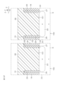
- One embodiment of the present disclosure includes a process for selectively forming a plurality of body regions spaced apart in a first direction in a surface layer of the semiconductor region by selectively injecting a second conductivity type impurity into the semiconductor region, and a process for forming a first mask that selectively covers each of the body regions, the first mask including a first portion that extends in a second direction perpendicular to the first direction and has a first width in the first direction, and a pair of protrusions that protrude from a center of the first portion in the second direction to both sides in the first direction, and a process for injecting the first conductivity type impurity into the body region through the first mask.
- the semiconductor device and manufacturing method thereof according to one embodiment of the present disclosure can form impurity regions with high precision even in fine patterns.
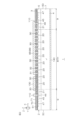
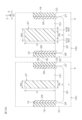
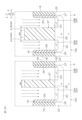
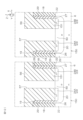
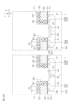
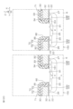
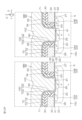
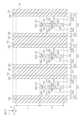
- FIG. 1 is a plan view showing a semiconductor device according to an embodiment.
- FIG. 2 is a cross-sectional view taken along the line II-II shown in FIG.
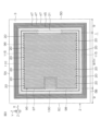
- FIG. 3 is a plan view showing an example of the layout of the first main surface.
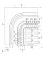
- FIG. 4 is an enlarged plan view showing a main portion of the first main surface.
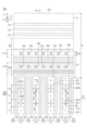
- FIG. 5 is an enlarged plan view showing further essential parts of the first main surface.
- FIG. 6 is an enlarged plan view showing the main part of FIG.
- FIG. 7 is a cross-sectional view taken along line VII-VII shown in FIG.
- FIG. 8 is a cross-sectional view taken along line VIII-VIII shown in FIG.
- FIG. 9 is a cross-sectional view taken along line IX-IX shown in FIG.
- FIG. 1 is a plan view showing a semiconductor device according to an embodiment.
- FIG. 2 is a cross-sectional view taken along the line II-II shown in FIG.
- FIG. 3 is a plan view
- FIG. 10 is a cross-sectional view taken along line X-X shown in FIG.
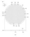
- FIG. 11 is a schematic diagram showing a wafer.
- FIG. 12A is a cross-sectional view showing a method for manufacturing a semiconductor device.
- FIG. 12B is a cross-sectional view showing a step subsequent to that of FIG. 12A.
- FIG. 12C is a cross-sectional view showing a step subsequent to FIG. 12B.
- FIG. 12D is a cross-sectional view showing a step subsequent to FIG. 12C.
- FIG. 12E is a cross-sectional view showing a step subsequent to FIG. 12D.
- FIG. 12F is a cross-sectional view showing a step subsequent to FIG. 12E.
- FIG. 12A is a cross-sectional view showing a method for manufacturing a semiconductor device.
- FIG. 12B is a cross-sectional view showing a step subsequent to that of FIG. 12A.
- FIG. 12C is a cross-section
- FIG. 12G is a cross-sectional view showing a step subsequent to FIG. 12F.
- FIG. 12H is a cross-sectional view showing a step subsequent to FIG. 12G.
- FIG. 12I is a cross-sectional view showing a step subsequent to FIG. 12H.
- FIG. 12J is a cross-sectional view showing a step subsequent to FIG. 12I.
- FIG. 12K is a cross-sectional view showing a step subsequent to FIG. 12J.
- FIG. 12L is a cross-sectional view showing a step subsequent to FIG. 12K.
- FIG. 12M is a cross-sectional view showing a step subsequent to FIG. 12L.
- FIG. 12N is a cross-sectional view showing a step subsequent to FIG. 12M.
- FIG. 12G is a cross-sectional view showing a step subsequent to FIG. 12F.
- FIG. 12H is a cross-sectional view showing a step subsequent to FIG. 12G.
- FIG. 12I
- FIG. 12O is a cross-sectional view showing a step subsequent to FIG. 12N.
- FIG. 12P is a cross-sectional view showing a step subsequent to that shown in FIG. 12O.
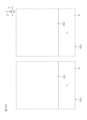
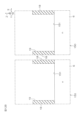
- FIG. 13 is a diagram showing a plane pattern of the first mask shown in FIG. 12G.
- FIG. 14 is a cross-sectional view showing a modification of the source region and the body contact region of FIG.
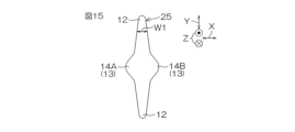
- FIG. 15 is a diagram showing a first modified example of the body contact region.
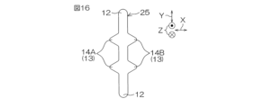
- FIG. 16 is a diagram showing a second modified example of the body contact region.
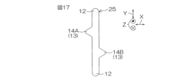
- FIG. 17 is a diagram showing a third modified example of the body contact region.
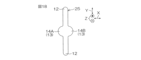
- FIG. 18 is a diagram showing a fourth modification of the body contact region.
- FIG. 19 is a diagram showing a fifth modification of the body contact region.
- this term includes a numerical value (shape) that is equal to the numerical value (shape) of the comparison target, as well as a numerical error (shape error) within a range of ⁇ 10% based on the numerical value (shape) of the comparison target.
- shape a numerical value that is equal to the numerical value (shape) of the comparison target
- error a numerical error within a range of ⁇ 10% based on the numerical value (shape) of the comparison target.
- the conductivity type of a semiconductor is indicated using “p-type” or “n-type”, but “p-type” may also be referred to as the “first conductivity type” and “n-type” as the “second conductivity type”. Of course, “n-type” may also be referred to as the "first conductivity type” and “p-type” as the “second conductivity type”.
- P-type is a conductivity type resulting from a trivalent element
- n-type is a conductivity type resulting from a pentavalent element.
- the trivalent element is at least one of boron, aluminum, gallium, and indium.
- the pentavalent element is at least one of nitrogen, phosphorus, arsenic, antimony, and bismuth.
- FIG. 1 is a plan view showing a semiconductor device 1 according to an embodiment.
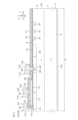
- FIG. 2 is a cross-sectional view taken along line II-II shown in FIG. 1.
- FIG. 3 is a plan view showing an example layout of a first main surface 3.
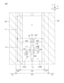
- FIG. 4 is an enlarged plan view showing a main portion of the first main surface 3.
- FIG. 5 is an enlarged plan view showing further main portions of the first main surface 3.
- FIG. 6 is an enlarged plan view showing the main parts of FIG. 5.
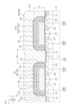
- FIG. 7 is a cross-sectional view taken along line VII-VII shown in FIG. 5.
- FIG. 8 is a cross-sectional view taken along line VIII-VIII shown in FIG. 5.
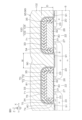
- FIG. 9 is a cross-sectional view taken along line IX-IX shown in FIG. 5.
- FIG. 10 is a cross-sectional view taken along line X-X shown in FIG. 5.
- semiconductor device 1 is a semiconductor switching device having an insulated gate type transistor structure Tr as an example of a device structure.
- the transistor structure Tr has a vertical structure.
- Semiconductor device 1 is a SiC semiconductor device having a chip 2 including a SiC single crystal. Chip 2 may be referred to as a "SiC chip” or a "semiconductor chip.”
- the chip 2 is made of hexagonal SiC single crystal and is formed into a rectangular parallelepiped shape.
- the hexagonal SiC single crystal has a number of polytypes including 2H (Hexagonal)-SiC single crystal, 4H-SiC single crystal, 6H-SiC single crystal, etc.
- the chip 2 is made of 4H-SiC single crystal, but the chip 2 may be made of other polytypes.
- the chip 2 has a first main surface 3 on one side, a second main surface 4 on the other side, and first to fourth side surfaces 5A to 5D connecting the first main surface 3 and the second main surface 4.
- the first main surface 3 and the second main surface 4 are formed in a quadrangular shape in a plan view seen from the vertical direction Z (hereinafter simply referred to as "plan view").
- the vertical direction Z is also the thickness direction of the chip 2 and the normal direction of the first main surface 3 (second main surface 4).
- the first main surface 3 and the second main surface 4 may be formed in a square or rectangular shape in a plan view.
- the first main surface 3 and the second main surface 4 are preferably formed by the c-plane of the SiC single crystal.
- the first main surface 3 is formed by the silicon surface ((0001) surface) of the SiC single crystal
- the second main surface 4 is formed by the carbon surface ((000-1) surface) of the SiC single crystal.
- the first side surface 5A and the second side surface 5B extend in a first direction X along the first main surface 3 and face a second direction Y that intersects with the first direction X along the first main surface 3. Specifically, the second direction Y is perpendicular to the first direction X.
- the third side surface 5C and the fourth side surface 5D extend in the second direction Y and face the first direction X.
- first direction X refers to the third side surface 5C side
- second direction Y refers to the first side surface 5A side
- second side of the second direction Y refers to the second side surface 5B side.
- first direction X is the m-axis direction ([1-100] direction) of the SiC single crystal
- the second direction Y is the a-axis direction ([11-20] direction) of the SiC single crystal.
- first direction X may be the a-axis direction of the SiC single crystal
- second direction Y may be the m-axis direction of the SiC single crystal.
- the chip 2 (first main surface 3 and second main surface 4) has an off angle that is inclined at a predetermined angle in a predetermined off direction with respect to the c-plane of the SiC single crystal.
- the c-axis ((0001) axis) of the SiC single crystal is inclined from the vertical axis toward the off direction by the off angle.
- the c-plane of the SiC single crystal is inclined by the off angle with respect to the horizontal plane.
- the off-direction is preferably the a-axis direction of the SiC single crystal (i.e., the second direction Y).
- the off-angle may be greater than 0° and less than or equal to 10°.
- the off-angle may have a value that falls within at least one of the following ranges: greater than 0° and less than or equal to 1°, 1° or more and less than or equal to 2.5°, 2.5° or more and less than or equal to 5°, 5° or more and less than or equal to 7.5°, and 7.5° or more and less than or equal to 10°.
- the off angle is preferably 5° or less. It is particularly preferable that the off angle be 2° or more and 4.5° or less.
- the off angle is typically set in the range of 4° ⁇ 0.1°. This specification does not exclude a configuration in which the off angle is 0° (i.e., a configuration in which the first main surface 3 is a just plane relative to the c-plane).
- the semiconductor device 1 includes an n-type first semiconductor region 6 formed in a region (surface layer) on the first main surface 3 side in the chip 2.
- the first semiconductor region 6 may be referred to as a "drift region,” “drain drift region,” “drain region,” etc.
- a drain potential is applied to the first semiconductor region 6 as a high potential (first potential).
- the first semiconductor region 6 is formed in a layer extending along the first main surface 3, and is exposed from the first main surface 3 and the first to fourth side surfaces 5A to 5D.
- the first semiconductor region 6 is made of an epitaxial layer (specifically, a SiC epitaxial layer).
- the semiconductor device 1 includes an n-type second semiconductor region 7 formed in a region (surface layer) on the second main surface 4 side in the chip 2. A drain potential is applied to the second semiconductor region 7.
- the second semiconductor region 7 may be referred to as a "drain region” or the like.
- the second semiconductor region 7 has a higher n-type impurity concentration than the first semiconductor region 6, and is electrically connected to the first semiconductor region 6 in the chip 2.
- the second semiconductor region 7 is formed in a layer extending along the second main surface 4, and is exposed from the second main surface 4 and the first to fourth side surfaces 5A to 5D.
- the second semiconductor region 7 is made of a semiconductor substrate (specifically, a SiC substrate).
- the chip 2 has a layered structure including a semiconductor substrate and an epitaxial layer.
- the second semiconductor region 7 has a thickness greater than that of the first semiconductor region 6.
- the semiconductor device 1 includes an active region 8 set in the chip 2.
- the active region 8 includes a device structure (transistor structure Tr) and is a region where an output current (drain current) is generated.
- the active region 8 is set in the inner part of the chip 2 at a distance from the periphery (first to fourth side faces 5A to 5D) of the chip 2 in a plan view.
- the active region 8 is set in a polygonal shape (a square shape in this embodiment) having four sides parallel to the periphery of the chip 2 in a plan view.
- the planar area of the active region 8 is preferably 50% to 90% of the planar area of the first main surface 3.
- the semiconductor device 1 includes a peripheral region 9 that is set outside the active region 8 in the chip 2.
- the peripheral region 9 is provided in a region between the periphery of the chip 2 and the active region 8 in a planar view.
- the peripheral region 9 extends in a band shape along the active region 8 in a planar view, and is set in a polygonal ring shape (a square ring in this embodiment) that surrounds the active region 8.
- the semiconductor device 1 includes a plurality of p-type body regions 20 formed in a surface layer portion of the first main surface 3 in the active region 8.
- a source potential is applied to the plurality of body regions 20 as a low potential (second potential) different from a high potential (first potential).
- the plurality of body regions 20 are arranged at intervals in the first direction X, and are each formed in a band shape extending in the second direction Y. In other words, the plurality of body regions 20 are arranged in a stripe shape extending in the second direction Y.
- the multiple body regions 20 are formed at intervals from the bottom of the first semiconductor region 6 toward the first main surface 3, and face the second semiconductor region 7 across a portion of the first semiconductor region 6. It is preferable that the multiple body regions 20 are formed at intervals from the middle of the first semiconductor region 6 toward the first main surface 3. The multiple body regions 20 are exposed from the first main surface 3.
- the semiconductor device 1 includes a p-type outer body region 21 formed in the surface layer of the first main surface 3 in the peripheral region 9.
- the outer body region 21 preferably has a p-type impurity concentration that is approximately equal to the p-type impurity concentration of the body region 20.
- the p-type impurity concentration of the outer body region 21 may be less than the p-type impurity concentration of the body region 20, or may be higher than the p-type impurity concentration of the body region 20.
- the outer body region 21 is formed at a distance from the periphery of the first main surface 3 (first to fourth side surfaces 5A to 5D) toward the active region 8, and extends in a band along the active region 8.
- the outer body region 21 has a portion that extends in a band in the first direction X and a portion that extends in a band in the second direction Y in a plan view, and divides the active region 8 from multiple directions.
- the outer body region 21 surrounds the active region 8 in a plan view and is partitioned into a polygonal ring (a square ring in this embodiment) having four sides parallel to the periphery of the first main surface 3.
- the outer body region 21 forms the boundary between the active region 8 and the peripheral region 9.
- the outer body region 21 may have an edge portion that connects the portion extending in the first direction X and the portion extending in the second direction Y in a circular arc shape (preferably a quadrant arc shape) in a plan view (see FIG. 4).
- the outer body region 21 has an inner edge on the active region 8 side and an outer edge on the peripheral side of the first main surface 3.
- the inner edge of the outer body region 21 is connected to the multiple body regions 20 in a portion extending in the first direction X. As a result, the outer body region 21 is fixed to the same potential as the multiple body regions 20.
- the outer body region 21 preferably has a width greater than the width of the body region 20.
- the width of the body region 20 is the width in a direction perpendicular to the extension direction (i.e., the first direction X).
- the width of the outer body region 21 is the width in a direction perpendicular to the extension direction.
- the width of the outer body region 21 may be approximately equal to the width of the body region 20, or may be less than the thickness of the body region 20.
- the ratio of the width of the outer body region 21 to the width of the body region 20 may be greater than or equal to 10 and less than or equal to 50. It is preferable that the width ratio be greater than or equal to 20 and less than or equal to 40.
- the outer body region 21 is formed at a distance from the bottom of the first semiconductor region 6 toward the first main surface 3, and faces the second semiconductor region 7 across a portion of the first semiconductor region 6. It is preferable that the outer body region 21 is formed at a distance from the middle of the first semiconductor region 6 toward the first main surface 3. The outer body region 21 is exposed from the first main surface 3.
- the outer body region 21 has a thickness (depth) that is approximately equal to the thickness (depth) of the body region 20.
- the thickness of the outer body region 21 may be less than the thickness of the body region 20, or may be greater than the thickness of the body region 20.
- the semiconductor device 1 includes a plurality of n-type surface drift regions 22 formed in a surface portion of the first main surface 3.
- the plurality of surface drift regions 22 each consist of a portion of the first semiconductor region 6.
- the plurality of surface drift regions 22 may have an n-type impurity concentration higher than the n-type impurity concentration of the first semiconductor region 6, or may have an n-type impurity concentration lower than the n-type impurity concentration of the first semiconductor region 6.
- the multiple surface drift regions 22 are each defined in a region between multiple adjacent body regions 20 in the first direction X. Specifically, the multiple surface drift regions 22 are each defined by multiple body regions 20 and outer body regions 21 in the surface portion of the first main surface 3. The multiple surface drift regions 22 are arranged at intervals in the first direction X, and are each formed in a band shape extending in the second direction Y. In other words, the multiple surface drift regions 22 are formed in a stripe shape extending in the second direction Y.
- the semiconductor device 1 includes n-type source regions 23 formed in the surface layer of each of the body regions 20.
- the source regions 23 have an n-type impurity concentration higher than the n-type impurity concentration of the first semiconductor region 6.
- a source potential is applied to the source regions 23.
- the semiconductor device 1 includes a plurality of p-type contact regions 25 formed in the surface layer of each of the body regions 20 in the active region 8.
- the contact regions 25 may be referred to as "backgate regions.”
- a source potential is applied to the contact regions 25.
- the contact regions 25 have a p-type impurity concentration higher than the p-type impurity concentration of the body regions 20.
- each body region 20 has a plurality of first sections 10 and a plurality of second sections 11 alternating in the second direction Y. There need not be a clear boundary between the first sections 10 and the second sections 11. In Figures 5 and 6, for clarity, the boundary between the first section 10 and the second section 11 is shown by a dashed line. As shown in Figures 5 and 6, the first section 10 and the second section 11 may have the same length in the second direction Y or may have different lengths. For example, the first section 10 may be longer than the second section 11 in the second direction Y, and the first section 10 may be shorter than the second section 11.
- the multiple contact regions 25 are arranged at intervals for each first section 10 so as to skip each second section 11 in the second direction Y.
- the contact region 25 and the regions on both sides of the contact region 25 in the first direction X may be the first sections 10.
- the second sections 11 may be the regions between the multiple contact regions 25 adjacent to each other in the second direction Y.
- Each contact region 25 extends in a band shape along the extension direction (second direction Y) of the body region 20.
- the contact region 25 is formed at a distance from the outer body region 21 in the second direction Y. In other words, the contact region 25 is not formed in the outer body region 21.
- the contact region 25 is formed at a distance from the bottom of the body region 20 toward the first main surface 3, and faces the first semiconductor region 6 with a part of the body region 20 in between.
- Each contact region 25 is formed at a distance from both the periphery on one side and the other side of the body region 20 in the first direction X. In this embodiment, the contact region 25 is formed in the center of the body region 20 in the first direction X.
- the source region 23 is separated into a plurality of source regions 24A, 24B in the first section 10.
- one contact region 25 is interposed in the region between the first source region 24A and the second source region 24B in the surface layer portion of the corresponding body region 20.
- Each contact region 25 is sandwiched between the first source region 24A and the second source region 24B in the first direction X.
- the multiple source regions 24A, 24B include a first source region 24A located on one side of the first direction X and a second source region 24B located on the other side of the first direction X in the surface layer portion of each body region 20.
- one first source region 24A is formed on one end side of the body region 20 in the first direction X
- one second source region 24B is formed on the other end side of the body region 20.
- the contact region 25 includes a first portion 12 extending in a band shape in the second direction Y, and a plurality of protrusions 13 protruding outward in the first direction X from the first portion 12.
- the first portion 12 crosses the first section 10 of the body region 20 in the second direction Y, and has an end at the boundary between the first section 10 and the second section 11.
- the first portion 12 may be referred to by another name depending on its planar shape.
- the first portion 12 when the shape assumed excluding the convex portion 13 (the shape in which the parts facing each other above and below the convex portion 13 in the second direction Y are connected by a dashed line 17) is a band in a planar view, the first portion 12 may be referred to as a band-shaped portion.
- the width (first width W1) of the first portion 12 may be, for example, 0.2 ⁇ m or more and 0.6 ⁇ m or less.
- the first width W1 may be constant or approximately constant in the second direction Y.
- the multiple protrusions 13 may include a pair of protrusions 14A, 14B that protrude from the center of the first portion 12 in the second direction Y to both sides in the first direction X. That is, one protrusion 13 is formed on one side and one on the other side in the first direction X of the first portion 12.
- the protrusion 13 that protrudes toward the first source region 24A is the first protrusion 14A
- the protrusion 13 that protrudes toward the second source region 24B is the second protrusion 14B.
- the first protrusion 14A and the second protrusion 14B protrude toward opposite sides from the same position on the first portion 12.
- Each of the protrusions 14A, 14B may protrude from the first portion 12 and have a polygonal shape in a plan view having one or more apexes 49.
- each of the protrusions 14A, 14B is formed in a triangular shape in a plan view.
- the apexes 49 have a rounded shape.
- the pair of protrusions 14A, 14B may have a diamond or circular overall shape in plan view, protruding evenly on both sides of the first portion 12.
- the overall shape of the pair of protrusions 14A, 14B may be a shape defined by the outline 15 of the pair of protrusions 14A, 14B and an inner extension line 16 (virtual line) of the outline 15 toward the inside of the contact region 25 (first portion 12).
- a diamond pattern is shown as the overall shape of the pair of protrusions 14A, 14B.
- the overall width (second width W2) of the pair of protrusions 14A, 14B from the end of the first protrusion 14A in the first direction X to the end of the second protrusion 14B in the first direction X may be 1.2 ⁇ m or more and 1.6 ⁇ m or less.
- the width WS of each of the first source region 24A and the second source region 24B on both sides of the first portion 12 in the first direction X may be greater than the overall width (second width W2) of the pair of protrusions 14A, 14B.
- the width WS may be, for example, 2 ⁇ m or more and 4 ⁇ m or less.
- the semiconductor device 1 includes a plurality of p-type channel regions 26, 27 formed in a surface portion of the first main surface 3.
- the plurality of channel regions 26, 27 are partitioned in the surface portion of the plurality of body regions 20 in regions between the ends of the plurality of body regions 20 (the plurality of surface drift regions 22) and the periphery of the source region 23.
- the plurality of channel regions 26, 27 are arranged at intervals in the first direction X and are each formed in a band shape extending in the second direction Y.
- the plurality of channel regions 26, 27 are arranged in stripes extending in the second direction Y.
- the multiple channel regions 26, 27 include multiple first channel regions 26 and multiple second channel regions 27.
- the multiple first channel regions 26 are formed in the region on the multiple first source regions 24A side, and form a current path extending in the horizontal direction.
- the multiple second channel regions 27 are formed in the region on the multiple second source regions 24B side, and form a current path extending in the horizontal direction.
- the semiconductor device 1 includes a plurality of planar electrode type gate structures 30 arranged on the first main surface 3 in the active region 8.
- the plurality of gate structures 30 are arranged at intervals in the first direction X, and are each formed in a band shape extending in the second direction Y. In other words, the plurality of gate structures 30 are arranged in stripes extending in the second direction Y.
- the extension direction of the plurality of gate structures 30 coincides with the off-direction of the SiC single crystal.
- Each gate structure 30 is disposed on at least one channel region 26, 27.
- each gate structure 30 is disposed across one surface drift region 22 and straddles two adjacent body regions 20, covering a plurality of channel regions 26, 27.
- each gate structure 30 is disposed across the source region 23 on one body region 20 side and the source region 23 on the other body region 20 side, covering the surface drift region 22, the source region 23 (first source region 24A and second source region 24B), the first channel region 26, and the second channel region 27.
- the gate structure 30 has a stacked structure including an insulating film 31 and a gate electrode 32.
- the gate structure 30 does not have an insulating sidewall structure (spacer) on the side of the gate electrode 32.
- the insulating film 31 may include at least one of a silicon oxide film, a silicon nitride film, and a silicon oxynitride film.
- the insulating film 31 has a single layer structure made of a silicon oxide film. It is particularly preferable that the insulating film 31 includes a silicon oxide film made of an oxide of the chip 2.
- the insulating film 31 covers the first main surface 3 in a film-like shape and is disposed on at least one of the channel regions 26, 27. In this embodiment, the insulating film 31 is disposed so as to cross one surface drift region 22 and straddle two adjacent body regions 20, covering multiple channel regions 26, 27.
- the insulating film 31 is disposed across the source region 23 on one body region 20 side and the source region 23 on the other body region 20 side, and covers the surface drift region 22, the source region 23 (first source region 24A and second source region 24B), the first channel region 26, and the second channel region 27.
- the insulating film 31 partially covers the first source region 24A at a distance from the contact region 25, and exposes a part of the first source region 24A and the contact region 25 from the first main surface 3.
- the insulating film 31 partially covers the second source region 24B at a distance from the contact region 25, and exposes a part of the second source region 24B and the contact region 25 from the first main surface 3.
- the insulating film 31 partially covers the source region 23, and exposes a part of the source region 23 from the first main surface 3.
- the thickness of the insulating film 31 may be 10 nm or more and 150 nm or less.
- the thickness of the insulating film 31 may be a value that belongs to at least one of the following ranges: 10 nm or more and 25 nm or less, 25 nm or more and 50 nm or less, 50 nm or more and 75 nm or less, 75 nm or more and 100 nm or less, 100 nm or more and 125 nm or less, and 125 nm or more and 150 nm or less.
- the thickness of the insulating film 31 is preferably 25 nm or more and 75 nm or less.
- the gate electrode 32 is disposed on the insulating film 31 and faces at least one of the channel regions 26, 27 across the insulating film 31.
- a gate potential is applied to the gate electrode 32 as a control potential.
- the gate electrode 32 controls the inversion and non-inversion of at least one of the channel regions 26, 27 in response to the gate potential.
- the gate electrode 32 includes a conductive semiconductor polycrystal.
- the gate electrode 32 may include either or both of p-type conductive polysilicon and n-type conductive polysilicon.
- the conductivity type of the gate electrode 32 is adjusted according to the gate threshold voltage to be achieved.
- the gate electrode 32 may be referred to as a "polysilicon gate", a “poly gate”, etc.
- the gate electrode 32 is formed in a strip shape extending in the second direction Y. In other words, the extension direction of the gate electrode 32 coincides with the off-direction of the SiC single crystal. In this embodiment, the gate electrode 32 is formed spaced inward from both ends of the insulating film 31 in the first direction X, exposing both ends of the insulating film 31. The gate electrode 32 is disposed on the insulating film 31 so as to straddle two adjacent body regions 20 across one surface drift region 22, and faces multiple channel regions 26, 27 across the insulating film 31.
- the gate electrode 32 is disposed so as to straddle the source region 23 on one body region 20 side and the source region 23 on the other body region 20 side, and faces the surface drift region 22, the source region 23 (first source region 24A and second source region 24B), the first channel region 26, and the second channel region 27 across the insulating film 31.
- the gate electrode 32 has an electrode surface 33, a first sidewall 34 on one side in the first direction X, and a second sidewall 35 on the other side in the first direction X.
- the electrode surface 33 extends along the insulating film 31 (first main surface 3).
- the electrode surface 33 may extend approximately parallel to the insulating film 31 (first main surface 3).
- the first side wall 34 is formed at a distance from one end of the insulating film 31 to the other end in the first direction X, and extends in the vertical direction Z.
- the second side wall 35 is formed at a distance from the other end of the insulating film 31 to the one end in the first direction X, and extends in the vertical direction Z.
- the first sidewall 34 and the second sidewall 35 may extend perpendicularly to the insulating film 31. That is, the gate electrode 32 may be formed in a quadrangular shape (flattened rectangular shape) in cross-sectional view. The first sidewall 34 and the second sidewall 35 may be inclined obliquely toward the electrode surface 33. That is, the gate electrode 32 may be formed in a tapered shape (preferably an isosceles trapezoidal shape) in cross-sectional view.
- the width of the gate structure 30 may be 1 ⁇ m or more and 10 ⁇ m or less.
- the width of the gate structure 30 is the width in a direction perpendicular to the extension direction (i.e., the first direction X).
- the width of the gate structure 30 is preferably 1 ⁇ m or more and 5 ⁇ m or less.
- the semiconductor device 1 includes a p-type termination region 45 formed on the first main surface 3 in the peripheral region 9.
- the termination region 45 may be referred to as a "well region", a “termination well region”, etc.
- the termination region 45 may have a p-type impurity concentration approximately equal to the p-type impurity concentration of the outer body region 21.
- the p-type impurity concentration of the termination region 45 may be higher than the p-type impurity concentration of the outer body region 21, or may be lower than the p-type impurity concentration of the outer body region 21.
- the termination region 45 is spaced inward from the periphery of the first main surface 3 and is formed in the region between the periphery of the first main surface 3 and the outer body region 21.
- the termination region 45 extends in a band shape along the outer body region 21 in a plan view.
- the termination region 45 has a portion that extends in a band shape in the first direction X and a portion that extends in a band shape in the second direction Y in a plan view, and divides the active region 8 from multiple directions.
- the termination region 45 is formed at a distance from the bottom of the first semiconductor region 6 toward the first main surface 3, and faces the second semiconductor region 7 across a portion of the first semiconductor region 6.
- the termination region 45 is preferably formed at a distance from the middle of the first semiconductor region 6 toward the first main surface 3.
- the termination region 45 may have a thickness (depth) approximately equal to the thickness (depth) of the outer body region 21.
- the thickness of the termination region 45 may be greater than the thickness of the outer body region 21, or may be less than the thickness of the outer body region 21.
- the termination region 45 (inner edge) has an overlap region 46 that overlaps the outer edge of the outer body region 21.
- the overlap region 46 is a high-concentration region that includes the outer edge of the outer body region 21 and the inner edge of the termination region 45.
- the overlap region 46 includes both the p-type impurities of the outer body region 21 and the p-type impurities of the termination region 45, and has a p-type impurity concentration that is higher than both the p-type impurity concentration of the outer body region 21 and the p-type impurity concentration of the termination region 45.
- the overlap region 46 extends in a band shape along the outer body region 21 in a plan view.
- the overlap region 46 has a portion that extends in a band shape in the first direction X and a portion that extends in a band shape in the second direction Y in a plan view, and divides the active region 8 from multiple directions.
- the overlap region 46 is divided into a polygonal ring shape (a square ring shape in this embodiment) having four sides parallel to the periphery of the first main surface 3.
- the width of the overlap region 46 is preferably greater than the width of the body region 20.
- the width of the overlap region 46 may be less than or equal to the width of the body region 20.
- the semiconductor device 1 may have a relatively high-concentration p-type well region (46) instead of the overlap region 46.
- the well region (46) has a p-type impurity concentration higher than both the p-type impurity concentration of the outer body region 21 and the p-type impurity concentration of the termination region 45.
- the well region (46) may be formed in either or both of the surface layer of the outer body region 21 and the surface layer of the termination region 45.
- the field region 47 may have a p-type impurity concentration that is approximately equal to the p-type impurity concentration of the body region 20 (termination region 45).
- the p-type impurity concentration of the field region 47 may be higher than the p-type impurity concentration of the body region 20 (termination region 45), or may be lower than the p-type impurity concentration of the body region 20 (termination region 45).
- the multiple field regions 47 are formed in the region between the periphery of the first main surface 3 and the active region 8, with a gap inward from the periphery of the first main surface 3. Specifically, the multiple field regions 47 are formed in the region between the periphery of the first main surface 3 and the outer body region 21. More specifically, the multiple field regions 47 are arranged in the region between the periphery of the first main surface 3 and the termination region 45, with a gap from the termination region 45 to the periphery side of the first main surface 3.
- the multiple field regions 47 are formed at intervals from the bottom of the first semiconductor region 6 toward the first main surface 3, and face the second semiconductor region 7 across a portion of the first semiconductor region 6. It is preferable that the multiple field regions 47 are formed at intervals from the middle of the first semiconductor region 6 toward the first main surface 3.
- the semiconductor device 1 includes a peripheral insulating film 51 that covers the first main surface 3 in the peripheral region 9.
- the peripheral insulating film 51 may include at least one of a silicon oxide film, a silicon nitride film, and a silicon oxynitride film.
- the peripheral insulating film 51 has a single-layer structure made of a silicon oxide film. It is particularly preferable that the peripheral insulating film 51 includes a silicon oxide film made of an oxide of the chip 2.
- the peripheral insulating film 51 is preferably made of the same type of insulating material as the insulating film 31.
- the peripheral insulating film 51 preferably has a thickness approximately equal to that of the insulating film 31.
- the peripheral insulating film 51 covers the first main surface 3 in the peripheral region 9 in the form of a film.
- the peripheral insulating film 51 collectively covers the outer body region 21, the termination region 45, and the multiple field regions 47.
- the peripheral insulating film 51 is connected to the multiple insulating films 31 on the active region 8 side. Specifically, the peripheral insulating film 51 is formed integrally with the multiple insulating films 31, and forms one insulating film together with the multiple insulating films 31.
- the semiconductor device 1 includes a gate wiring 52 arranged on the first main surface 3 in the peripheral region 9.
- the semiconductor device 1 does not have an insulating sidewall structure (spacer) on the side of the gate wiring 52.
- the gate wiring 52 is selectively routed on the first main surface 3 and has a portion that extends in a different direction from the multiple gate electrodes 32.
- the gate wiring 52 is connected to the multiple gate electrodes 32 and applies a gate signal to the multiple gate electrodes 32.
- the gate wiring 52 may be referred to as a "polysilicon gate wiring", a "poly gate wiring", a "second gate electrode”, etc.
- the gate wiring 52 includes a conductive semiconductor polycrystal.
- the gate wiring 52 may include either or both of p-type conductive polysilicon and n-type conductive polysilicon. It is preferable that the gate wiring 52 has the same conductivity type as the gate electrode 32. The conductivity type of the gate wiring 52 is adjusted according to the conductivity type of the gate electrode 32.
- the gate wiring 52 is disposed on the peripheral insulating film 51 in the peripheral region 9. Specifically, the gate wiring 52 is disposed on a portion of the peripheral insulating film 51 that covers the outer body region 21, and faces the outer body region 21 across the peripheral insulating film 51.
- the gate wiring 52 is formed at a distance from the periphery of the first main surface 3 toward the active region 8, and extends in a strip along the active region 8.
- the gate wiring 52 has a portion that extends in a strip in the first direction X and a portion that extends in a strip in the second direction Y in a plan view, and defines the active region 8 from multiple directions.
- the gate wiring 52 surrounds the active region 8 in a plan view and is partitioned into a polygonal ring (a square ring in this embodiment) having four sides parallel to the periphery of the first main surface 3.
- the gate wiring 52 may be end-shaped or endless.
- the gate wiring 52 extends in a strip shape (ring shape in this embodiment) along the outer body region 21 in a plan view and faces the outer body region 21 across the outer insulating film 51 over the entire area in the stacking direction.
- the gate wiring 52 may have an edge portion that connects the portion extending in the first direction X and the portion extending in the second direction Y in a plan view in an arc shape (preferably a quadrant arc shape) (see FIG. 4).
- the gate wiring 52 is formed narrower than the outer body region 21 in a plan view, and is disposed above the outer body region 21 at a distance from the inner and outer edges of the outer body region 21.
- the multiple gate electrodes 32 are extended up to above the outer body region 21, and the gate wiring 52 is connected to the multiple gate electrodes 32 above the outer body region 21.
- the width of the gate wiring 52 is preferably greater than the width of the gate electrode 32.
- the width of the gate wiring 52 is the width in a direction perpendicular to the extension direction.
- the width of the gate wiring 52 may be less than or equal to the width of the gate electrode 32.
- the width of the gate wiring 52 may be greater than the width of the outer body region 21.
- the thickness of the gate wiring 52 is preferably approximately equal to the thickness of the gate electrode 32.
- the gate wiring 52 has a wiring surface 53, a first wiring sidewall 54 on the inner edge side, and a second wiring sidewall 55 on the outer edge side.
- the wiring surface 53 extends along the peripheral insulating film 51 (first main surface 3).
- the wiring surface 53 may extend approximately parallel to the peripheral insulating film 51 (first main surface 3).
- the first wiring sidewall 54 extends in the vertical direction Z on the peripheral insulating film 51, and the second wiring sidewall 55 extends in the vertical direction Z on the peripheral insulating film 51.
- the first wiring sidewall 54 is connected to the multiple gate electrodes 32 (the first sidewall 34 and the second sidewall 35) in the portion extending in the first direction X.
- the gate wiring 52 has multiple portions connected in a T-shape to the multiple gate electrodes 32. As a result, the gate wiring 52 is fixed to the same potential as the multiple gate electrodes 32.
- the first wiring sidewall 54 and the second wiring sidewall 55 may extend perpendicularly to the peripheral insulating film 51. That is, the gate wiring 52 may be formed in a quadrangular shape (flattened rectangular shape) in cross section. The first wiring sidewall 54 and the second wiring sidewall 55 may be inclined obliquely toward the wiring surface 53. That is, the gate wiring 52 may be formed in a tapered shape (preferably an isosceles trapezoidal shape) in cross section.
- the semiconductor device 1 includes an insulating interlayer film 70 that covers the first main surface 3.
- the interlayer film 70 may also be called an "interlayer insulating film,” an “intermediate insulating film,” or the like.
- the interlayer film 70 has an insulating surface 71 that extends along the first main surface 3.
- the interlayer film 70 collectively covers the active region 8 and the peripheral region 9 on the first main surface 3.
- the interlayer film 70 covers the multiple gate structures 30 in the active region 8. For each gate structure 30, the interlayer film 70 directly covers both the insulating film 31 and the gate electrode 32. In other words, the interlayer film 70 has a portion that directly covers the electrode surface 33, the first sidewall 34, and the second sidewall 35 of the gate electrode 32.
- the interlayer film 70 collectively covers the outer body region 21, the termination region 45, and the multiple field regions 47 in the peripheral region 9, sandwiching the peripheral insulating film 51 therebetween.
- the interlayer film 70 directly covers both the peripheral insulating film 51 and the gate wiring 52. That is, the interlayer film 70 has a portion that directly covers the wiring surface 53, the first wiring sidewall 54, and the second wiring sidewall 55 of the gate wiring 52.
- the interlayer film 70 is continuous with the first to fourth side surfaces 5A to 5D.
- the interlayer film 70 may be formed at a distance inward from the first to fourth side surfaces 5A to 5D, exposing the peripheral portion of the first main surface 3 (first semiconductor region 6).
- the interlayer film 70 has a layered structure including a first oxide film 72 (first insulating film) and a second oxide film 73 (second insulating film) that are layered in this order from the first main surface 3 side.
- the interlayer film 70 has an insulating surface 71 formed by the second oxide film 73.
- the first oxide film 72 has a single layer structure made of a silicon oxide film with no added impurities.
- the first oxide film 72 may be referred to as an NSG film (Nondoped Silicate Glass film).
- the first oxide film 72 collectively covers the active region 8 and the peripheral region 9.
- the first oxide film 72 collectively covers the multiple gate structures 30 in the active region 8.
- the first oxide film 72 covers both the insulating film 31 and the gate electrode 32 of each gate structure 30 in a film-like manner.
- the first oxide film 72 has a first covering portion 74, a second covering portion 75, and a third covering portion 76.
- the first covering portion 74 extends horizontally in a film shape along the insulating film 31 (first main surface 3), and has a portion that contacts the first sidewall 34 (second sidewall 35) of the gate electrode 32.
- the first covering portion 74 (first oxide film 72) has a thickness less than the thickness of the gate electrode 32, and covers the insulating film 31 with a gap from the height position of the electrode surface 33 of the gate electrode 32 toward the insulating film 31.
- the second covering portion 75 is extended from the first covering portion 74 toward the electrode surface 33 in the stacking direction, and directly covers the first side wall 34 (second side wall 35) in a film-like manner.
- the third covering portion 76 is pulled out from the second covering portion 75 toward the electrode surface 33 and extends horizontally along the electrode surface 33 in the form of a film.
- the third covering portion 76 directly covers the entire area of the electrode surface 33 between the first side wall 34 and the second side wall 35. It is preferable that the third covering portion 76 forms an arc corner portion curved in an arc shape together with the second covering portion 75 in the portion covering the corner portion of the gate electrode 32.
- the arc corner portion may have a center of curvature on the gate electrode 32 side.
- the first oxide film 72 collectively covers the outer body region 21, the termination region 45, and the multiple field regions 47 in the peripheral region 9, sandwiching the peripheral insulating film 51 therebetween.
- the first oxide film 72 covers the gate wiring 52 in the peripheral region 9.
- the second oxide film 73 may have a single layer structure made of a silicon oxide film containing phosphorus, or a multilayer structure including a silicon oxide film containing phosphorus.
- the silicon oxide film containing phosphorus may contain boron.
- the silicon oxide film containing phosphorus may be called a PSG film (Phosphorus Silicon Glass film).
- the silicon oxide film containing both phosphorus and boron may be called a BPSG film (Boron Phosphorus Silicon Glass film).
- the second oxide film 73 may have a single layer structure made of a PSG film or a BPSG film laminated on the first oxide film 72.
- the second oxide film 73 may have a laminate structure including a PSG film laminated on the first oxide film 72 and a BPSG film laminated on the PSG film.
- the second oxide film 73 may have a laminate structure including a BPSG film laminated on the first oxide film 72 and a PSG film laminated on the BPSG film.
- the second oxide film 73 has a single layer structure made of a PSG film, as an example.
- the second oxide film 73 covers the first oxide film 72 in a film-like manner, and collectively covers the active region 8 and the peripheral region 9 with the first oxide film 72 in between.
- the second oxide film 73 collectively covers the multiple gate structures 30 in the active region 8 with the first oxide film 72 in between.
- the second oxide film 73 covers both the insulating film 31 and the gate electrode 32 in a film-like manner with the first oxide film 72 in between.
- the second oxide film 73 includes a first upper coating portion 80 and a second upper coating portion 81.
- the first upper coating portion 80 covers the first coating portion 74 of the first oxide film 72.
- the first upper coating portion 80 covers the insulating film 31 in the portion located above the first coating portion 74, sandwiching the first coating portion 74.
- the first upper covering portion 80 extends in a film-like shape in the stacking direction from above the first covering portion 74 along the second covering portion 75, and covers the first side wall 34 (second side wall 35) of the gate structure 30 with the second covering portion 75 in between.
- the second upper covering portion 81 covers the third covering portion 76 of the first oxide film 72.
- the second upper covering portion 81 extends horizontally in a film shape from the first upper covering portion 80 along the third covering portion 76, and covers the electrode surface 33 of the gate structure 30 with the third covering portion 76 in between.
- the second upper covering portion 81 covers the entire electrode surface 33 with the third covering portion 76 in between the first side wall 34 and the second side wall 35. It is preferable that the second upper covering portion 81 forms an arc corner portion curved in an arc shape together with the first upper covering portion 80 in the portion covering the corner portion of the gate wiring 52.
- the arc corner portion may have a center of curvature on the gate wiring 52 side.
- the second oxide film 73 collectively covers the outer body region 21, the termination region 45, and the multiple field regions 47 in the peripheral region 9, sandwiching the peripheral insulating film 51 and the first oxide film 72 between them.
- the second oxide film 73 covers the gate wiring 52 in the peripheral region 9, sandwiching the first oxide film 72 between them.
- the semiconductor device 1 includes a plurality of source openings 90 formed in the interlayer film 70 in the active region 8.
- the plurality of source openings 90 are formed in regions to the sides of the plurality of gate electrodes 32 at intervals from the plurality of gate electrodes 32, respectively, and expose the first main surface 3 (chip 2).
- the plurality of source openings 90 are formed in regions between the plurality of gate electrodes 32, respectively, and penetrate the insulating film 31 and the interlayer film 70.
- the multiple source openings 90 penetrate both the first oxide film 72 and the second oxide film 73, and have wall surfaces defined by both the first oxide film 72 and the second oxide film 73.
- the multiple source openings 90 have opening ends defined by arc corners of the interlayer film 70.
- the multiple source openings 90 expose the corresponding multiple source regions 23 (first source region 24A and second source region 24B) and contact region 25, respectively.
- a plurality of source openings 90 may be formed in a region between two gate structures 30 adjacent in the first direction X.
- the plurality of source openings 90 may be formed in a line in the second direction Y with a space therebetween.
- each source opening 90 may be formed in a quadrilateral shape (square shape) in a plan view, a rectangular shape extending in the first direction X, a rectangular shape extending in the second direction Y, a hexagonal shape, a circular shape, or the like.
- the source opening 90 may have a width W of 0.2 ⁇ m or more and 3 ⁇ m or less.
- the width W of the source opening 90 is preferably 0.3 ⁇ m or more and 1 ⁇ m or less.
- the source opening 90 may have a depth D of 0.2 ⁇ m or more and 2 ⁇ m or less.
- the depth D of the source opening 90 is preferably 0.5 ⁇ m or more and 1 ⁇ m or less.
- the source opening 90 preferably has an aspect ratio D/W of 0.3 or more and 3 or less.
- the aspect ratio D/W is defined by the ratio of the depth D of the source opening 90 to the width W of the source opening 90.
- the aspect ratio D/W is preferably 0.5 or more and 2 or less. It is particularly preferable that the aspect ratio D/W is greater than 1. With this configuration, the multiple gate structures 30 are arranged at a narrow pitch.
- the semiconductor device 1 includes a plurality of source recesses 91 formed in the first main surface 3 in the portions exposed from the plurality of source openings 90.
- the semiconductor device 1 does not necessarily have to have the source recesses 91. Therefore, a configuration that does not have the source recesses 91 may be adopted.
- the multiple source recesses 91 each have a planar shape that matches the planar shape of the corresponding source opening 90, and are recessed from the first main surface 3 toward the second main surface 4.
- the multiple source recesses 91 are formed at intervals from the bottoms of the corresponding body regions 20 toward the first main surface 3, exposing the corresponding multiple source regions 23 and contact regions 25.
- the multiple source recesses 91 are formed at intervals from the bottoms of the corresponding multiple source regions 23 (contact regions 25) toward the first main surface 3.
- the semiconductor device 1 includes at least one (in this embodiment, multiple) outer openings 92 formed in the interlayer film 70 in the peripheral region 9.
- the multiple outer openings 92 are formed in a portion of the interlayer film 70 that covers the termination region 45.
- the multiple outer openings 92 penetrate the interlayer film 70 and expose the termination region 45.
- the multiple outer openings 92 are formed in a portion of the interlayer film 70 that covers the overlap region 46 of the termination region 45 and expose the overlap region 46.
- the outer openings 92 may expose the outer body region 21 instead of or in addition to the termination region 45 (overlapping region 46).
- the outer openings 92 penetrate both the first oxide film 72 and the second oxide film 73, and have wall surfaces defined by both the first oxide film 72 and the second oxide film 73.
- the outer openings 92 have opening ends defined by arc corners of the interlayer film 70.
- the multiple outer openings 92 are formed at intervals along the termination region 45 (overlap region 46) (see Figures 4 and 5).
- the multiple outer openings 92 may be formed in a quadrangular (square), rectangular, hexagonal, circular, or other shape in a plan view.
- the multiple outer openings 92 may be formed in a band shape extending along the termination region 45 (overlap region 46) in a plan view.
- the outer openings 92 may have an aspect ratio D/W (preferably greater than 1) similar to the source openings 90.
- the semiconductor device 1 may have a single outer opening 92.
- the single outer opening 92 may be formed in a band shape extending along the termination region 45 (overlapping region 46).
- the single outer opening 92 may have a portion extending in a band shape in the first direction X and a portion extending in a band shape in the second direction Y in a plan view.
- the single outer opening 92 may be formed in a polygonal ring shape (a square ring in this embodiment) with four sides parallel to the periphery of the first main surface 3, either with or without ends.
- the single outer opening 92 may have an edge portion that connects the portion extending in the first direction X and the portion extending in the second direction Y in an arc shape (preferably a quadrant arc shape) following the termination region 45 (overlapping region 46) in a plan view (see FIG. 4).
- the semiconductor device 1 includes a plurality of outer recesses 93 formed in the portions of the first main surface 3 exposed from the plurality of outer openings 92.
- the semiconductor device 1 does not necessarily have to have the outer recesses 93. Therefore, a configuration that does not have the outer recesses 93 may be adopted.
- the multiple outer recesses 93 each have a planar shape that matches the planar shape of the corresponding outer opening 92, and are recessed from the first main surface 3 toward the second main surface 4.
- the multiple outer recesses 93 are formed at intervals from the bottom of the termination region 45 (overlap region 46) toward the first main surface 3, and each exposes the termination region 45 (overlap region 46).
- the semiconductor device 1 includes at least one (in this embodiment, multiple) gate openings 94 formed in the interlayer film 70 in the peripheral region 9.
- the multiple gate openings 94 are formed in a portion of the interlayer film 70 that covers the gate wiring 52.
- the multiple gate openings 94 penetrate the interlayer film 70 and expose the wiring surface 53 of the gate wiring 52.
- the multiple gate openings 94 penetrate both the first oxide film 72 and the second oxide film 73, and have wall surfaces defined by both the first oxide film 72 and the second oxide film 73.
- the multiple gate openings 94 have opening ends defined by arc corners of the interlayer film 70.
- the semiconductor device 1 may have a single gate opening 94.
- the single gate opening 94 may be formed in a strip shape extending along the gate wiring 52.
- the single gate opening 94 may have a portion extending in a strip shape in the first direction X and a portion extending in a strip shape in the second direction Y in a plan view.
- the single gate opening 94 may be formed in a polygonal ring shape (a square ring in this embodiment) with or without ends, having four sides parallel to the periphery of the first main surface 3.
- the single gate opening 94 may have an edge portion that connects the portion extending in the first direction X and the portion extending in the second direction Y in an arc shape (preferably a quadrant arc shape) in a plan view following the gate wiring 52 (see FIG. 4).
- the semiconductor device 1 includes a source pad electrode 95 disposed on the interlayer film 70.
- the source pad electrode 95 is a terminal electrode to which a source potential is applied from the outside.
- the source pad electrode 95 may also be referred to as a "first pad electrode,” a “first main surface electrode,” a “first terminal electrode,” etc.
- the source pad electrode 95 is disposed on a portion of the interlayer film 70 that covers the active region 8.
- the source pad electrode 95 covers the multiple gate electrodes 32 with the interlayer film 70 in between, and is electrically isolated from the multiple gate electrodes 32 by the interlayer film 70.
- the source pad electrode 95 is electrically connected to the multiple body regions 20, the outer body region 21, the multiple source regions 23 (first source region 24A and second source region 24B), the contact region 25, etc. through the multiple source openings 90.
- the source pad electrode 95 has a first pad portion 96, a second pad portion 97, and a third pad portion 98.
- the first pad portion 96 has a relatively large planar area and forms the main body of the source pad electrode 95.
- the first pad portion 96 is formed in a polygonal shape (a square shape in this embodiment) having four sides parallel to the periphery of the chip 2 in a plan view, and is biased toward the fourth side surface 5D relative to the center of the active region 8.
- the first pad portion 96 covers the multiple gate electrodes 32 with the interlayer film 70 in between, and is electrically connected to the multiple body regions 20, etc. via the multiple source openings 90.
- the second pad portion 97 has a planar area less than that of the first pad portion 96, and is pulled out in a strip shape (rectangular shape) from one end of the first pad portion 96 in the second direction Y (the end on the first side surface 5A side) toward the third side surface 5C.
- the second pad portion 97 covers the multiple gate electrodes 32 with the interlayer film 70 in between, and is electrically connected to the multiple body regions 20, etc. via the multiple source openings 90.
- the third pad portion 98 has a planar area less than that of the first pad portion 96, and is pulled out in a strip shape (rectangular shape) from the other end of the first pad portion 96 in the second direction Y (the end on the second side surface 5B side) toward the third side surface 5C, and faces the second pad portion 97 in the second direction Y.
- the third pad portion 98 covers the multiple gate electrodes 32 with the interlayer film 70 in between, and is electrically connected to the multiple body regions 20 etc. via the multiple source openings 90.
- the plane area of the third pad portion 98 may be approximately equal to the plane area of the second pad portion 97. Of course, the plane area of the third pad portion 98 may be greater than the plane area of the second pad portion 97, or may be less than the plane area of the second pad portion 97. Either or both of the second pad portion 97 and the third pad portion 98 may be used as a terminal portion for monitoring a current.
- the source pad electrode 95 does not necessarily have to have both the second pad portion 97 and the third pad portion 98 at the same time.
- the source pad electrode 95 may have only one of the second pad portion 97 and the third pad portion 98.
- the source pad electrode 95 may be composed of only the first pad portion 96, and may not have the second pad portion 97 or the third pad portion 98.
- the source pad electrode 95 includes a first underlying electrode film 100 and a first main electrode film 102.
- the first underlying electrode film 100 may be referred to as the "source underlying electrode film,” and the first main electrode film 102 may be referred to as the "source main electrode film.”
- the first underlying electrode film 100 forms the lower layer of the source pad electrode 95 (first pad portion 96, second pad portion 97, and third pad portion 98) and covers the interlayer film 70 in the active region 8.
- the first underlying electrode film 100 collectively covers the region of the interlayer film 70 in which the multiple source openings 90 are formed. In other words, the first underlying electrode film 100 penetrates into the multiple source openings 90 from above the insulating surface 71.
- the first underlying electrode film 100 has a portion that covers the insulating surface 71 of the interlayer film 70 in a film-like manner, and a portion that covers the wall surfaces of the multiple source openings 90 in a film-like manner.
- the first underlying electrode film 100 defines recesses in each of the multiple source openings 90.
- the first underlying electrode film 100 may have a portion that partially covers the gate wiring 52 with the interlayer film 70 in between.
- the first underlying electrode film 100 may be formed spaced inward from the gate wiring 52 in a plan view.
- the first base electrode film 100 has a layered structure including a first electrode film 103 layered on the interlayer film 70, and a second electrode film 104 layered on the first electrode film 103.
- the first electrode film 103 includes a Ti film
- the second electrode film 104 includes a TiN film.
- the first base electrode film 100 does not necessarily have to have a laminated structure, and may have a single layer structure consisting of either the first electrode film 103 (Ti film) or the second electrode film 104 (TiN film).
- the thickness of the first electrode film 103 may be 10 nm or more and 100 nm or less.
- the thickness of the second electrode film 104 may be 50 nm or more and 200 nm or less.
- the first electrode film 103 collectively covers the region of the interlayer film 70 in which the multiple source openings 90 are formed, and extends into the multiple source openings 90 from above the insulating surface 71.
- the first electrode film 103 has a portion that covers the insulating surface 71 of the interlayer film 70 in a film-like manner, and a portion that covers the wall surfaces of the multiple source openings 90 in a film-like manner.
- the first electrode film 103 directly covers the insulating surface 71.
- the first electrode film 103 directly covers the second oxide film 73 on the insulating surface 71.
- the first oxide film 72 faces the multiple gate electrodes 32 across the interlayer film 70 in the portion covering the insulating surface 71.
- the first electrode film 103 covers the arc corner of the interlayer film 70 (second oxide film 73) in a film-like manner, following the arc corner of the interlayer film 70 (second oxide film 73), and extends into the source opening 90.
- the first electrode film 103 has a portion that extends in an arc shape at the arc corner. This improves the film-forming property of the first electrode film 103 on the interlayer film 70 (the wall surface of the source opening 90).
- the first electrode film 103 extends along the wall surface of the source opening 90 and covers the insulating film 31, the first oxide film 72, and the second oxide film 73.
- the first electrode film 103 faces the first sidewall 34 (second sidewall 35) of the gate electrode 32 with the interlayer film 70 in between.
- the first electrode film 103 covers the first main surface 3 at the bottom of each source opening 90 in a film-like manner, and is electrically connected to the first main surface 3. Specifically, the first electrode film 103 has a portion that covers the bottom of each source opening 90 in a film-like manner, and is electrically connected to the multiple source regions 23 (first source region 24A and second source region 24B) and contact region 25.
- the second electrode film 104 covers the area of the interlayer film 70 on the first electrode film 103 where the multiple source openings 90 are formed.
- the second electrode film 104 has a portion that covers the insulating surface 71 of the interlayer film 70 in a film-like manner, sandwiching the first electrode film 103, and a portion that covers the wall surfaces of the multiple source openings 90 in a film-like manner, sandwiching the first electrode film 103.
- the second electrode film 104 faces the multiple gate electrodes 32 across the first electrode film 103 and the interlayer film 70 in the portion covering the insulating surface 71.
- the second electrode film 104 covers the arc corners of the interlayer film 70 (second oxide film 73) in a film-like manner and extends into the source opening 90.
- the second electrode film 104 has a portion that extends in an arc shape at the arc corners of the interlayer film 70. This improves the film-forming properties of the second electrode film 104 on the interlayer film 70 (the wall surface of the source opening 90).
- the second electrode film 104 extends along the wall surface of the source opening 90, and covers the insulating film 31, the first oxide film 72, and the second oxide film 73 with the first electrode film 103 in between.
- the second electrode film 104 faces the first sidewall 34 (second sidewall 35) of the gate electrode 32 with the first electrode film 103 and the interlayer film 70 in between.
- the second electrode film 104 has a portion that covers the bottom of each source opening 90 in a film-like manner, sandwiching the first electrode film 103 therebetween, and is electrically connected to the multiple source regions 23 (first source region 24A and second source region 24B) and the contact region 25.
- the first main electrode film 102 forms the upper layer of the source pad electrode 95 (first pad portion 96, second pad portion 97, and third pad portion 98) and covers the first base electrode film 100 in a film form.
- the first main electrode film 102 contains a conductive material different from the conductive material of the first base electrode film 100.
- the first main electrode film 102 may include at least one of an Al film, an Al alloy film, a Cu film, and a Cu alloy film.
- the Al alloy film may include at least one of an AlSi alloy film, an AlCu alloy film, and an AlSiCu alloy film.
- the first main electrode film 102 has a thickness greater than the thickness (total thickness) of the first base electrode film 100.
- the thickness of the first main electrode film 102 may be 0.5 ⁇ m or more and 5 ⁇ m or less.
- the thickness of the first main electrode film 102 may have a value that belongs to at least one of the following ranges: 0.5 ⁇ m or more and 1 ⁇ m or less, 1 ⁇ m or more and 1.5 ⁇ m or less, 1.5 ⁇ m or more and 2 ⁇ m or less, 2 ⁇ m or more and 2.5 ⁇ m or less, 2.5 ⁇ m or more and 3 ⁇ m or less, 3 ⁇ m or more and 3.5 ⁇ m or less, 3.5 ⁇ m or more and 4 ⁇ m or less, 4 ⁇ m or more and 4.5 ⁇ m or less, and 4.5 ⁇ m or more and 5 ⁇ m or less.
- the first main electrode film 102 is mechanically and electrically connected to the first underlying electrode film 100 in the portion covering the insulating surface 71. As a result, the first main electrode film 102 faces the multiple gate electrodes 32 with the first underlying electrode film 100 and the interlayer film 70 in between.
- the semiconductor device 1 includes a source finger electrode 110 that is extended from the source pad electrode 95 onto the peripheral region 9.
- the source finger electrode 110 transmits the source potential applied to the source pad electrode 95 to the peripheral region 9.
- the source finger electrode 110 is extended from the portion of the source pad electrode 95 (first pad portion 96) on the fourth side surface 5D side onto the portion of the interlayer film 70 that covers the peripheral region 9.
- the source finger electrodes 110 are extended to above the termination region 45 and are electrically connected to the termination region 45 via a plurality of outer openings 92. Specifically, the source finger electrodes 110 are electrically connected to the overlap region 46 of the termination region 45 via a plurality of outer openings 92.
- the source finger electrode 110 extends in a strip shape along the termination region 45 (overlapping region 46).
- the source finger electrode 110 has a portion extending in a strip shape in the first direction X in a plan view and a portion extending in a strip shape in the second direction Y.
- the source finger electrode 110 is formed in a polygonal ring shape (a square ring shape in this embodiment) having four sides parallel to the periphery of the first main surface 3, and surrounds the source pad electrode 95.
- the source finger electrode 110 may have an edge portion that connects the portion extending in the first direction X and the portion extending in the second direction Y in a plan view in an arc shape (preferably a quadrant arc shape) (see FIG. 4).
- the source finger electrode 110 like the source pad electrode 95, includes a first underlying electrode film 100 and a first main electrode film 102.
- the first underlying electrode film 100 forms the lower layer of the source finger electrode 110 and covers the interlayer film 70 in the peripheral region 9.
- the first underlying electrode film 100 collectively covers the region of the interlayer film 70 where the multiple outer openings 92 are formed. In other words, the first underlying electrode film 100 extends into the multiple outer openings 92 from above the insulating surface 71.
- the first underlying electrode film 100 has a portion that covers the insulating surface 71 of the interlayer film 70 in a film-like manner, and a portion that covers the wall surfaces of the multiple outer openings 92 in a film-like manner.
- the first underlying electrode film 100 defines recesses in each of the multiple outer openings 92.
- the first underlying electrode film 100 has a layered structure including a first electrode film 103 and a second electrode film 104, similar to the source pad electrode 95.
- the first main electrode film 102 forms the upper layer of the source finger electrode 110 and covers the first underlying electrode film 100 in a film-like manner.
- the first main electrode film 102 is mechanically and electrically connected to the first underlying electrode film 100 in the portion covering the insulating surface 71.
- the first main electrode film 102 is electrically connected to the termination region 45 (overlap region 46) via the first underlying electrode film 100.
- the semiconductor device 1 includes a gate finger electrode 115 selectively routed over the interlayer film 70.
- the gate finger electrode 115 transmits a gate potential to the gate wiring 52.
- the gate finger electrode 115 is routed over a portion of the interlayer film 70 that covers the gate wiring 52 (i.e., over the outer peripheral region 9), and is electrically connected to the gate wiring 52 through a plurality of gate openings 94.
- the gate finger electrode 115 is disposed in a region between the source pad electrode 95 and the source finger electrode 110 and spaced apart from the source pad electrode 95 and the source finger electrode 110.
- the gate finger electrode 115 is disposed on the gate wiring 52 and extends in a strip shape along the gate wiring 52.
- the gate finger electrode 115 has a portion that extends in a strip shape in the first direction X and a portion that extends in a strip shape in the second direction Y in a plan view.
- the gate finger electrode 115 is formed in a band shape with four sides parallel to the periphery of the first main surface 3, and surrounds the source pad electrode 95.
- the gate finger electrode 115 may have an edge portion that connects the portion extending in the first direction X and the portion extending in the second direction Y in a circular arc shape (preferably a quadrant arc shape) in a plan view (see FIG. 4).
- the gate finger electrode 115 has a pair of open ends on the fourth side surface 5D side through which the source finger electrode 110 passes.
- the gate finger electrode 115 includes a second underlying electrode film 120 and a second main electrode film 122.
- the second underlying electrode film 120 may be referred to as the "gate underlying electrode film,” and the second main electrode film 122 may be referred to as the "gate main electrode film.”
- the second underlying electrode film 120 forms a lower layer of the gate finger electrode 115, and covers the interlayer film 70 in the peripheral region 9.
- the second underlying electrode film 120 collectively covers the region of the interlayer film 70 in which the multiple gate openings 94 are formed. In other words, the second underlying electrode film 120 penetrates into the multiple gate openings 94 from above the insulating surface 71.
- the second underlying electrode film 120 has a portion that covers the insulating surface 71 of the interlayer film 70 in a film-like manner, and a portion that covers the wall surfaces of the multiple gate openings 94 in a film-like manner.
- the second underlying electrode film 120 defines multiple recesses within the multiple gate openings 94.
- the second underlying electrode film 120 has a layered structure similar to that of the first electrode film 103 and the second electrode film 104 of the first underlying electrode film 100.
- the layered structure of the second underlying electrode film 120 is similar to that of the first electrode film 103 and the second electrode film 104 of the first underlying electrode film 100, so a description thereof will be omitted.
- the second main electrode film 122 forms the upper layer of the gate finger electrode 115 and covers the second base electrode film 120 in a film form.
- the second main electrode film 122 contains a conductive material different from the conductive material of the second base electrode film 120.
- the second main electrode film 122 may include at least one of an Al film, an Al alloy film, a Cu film, and a Cu alloy film.
- the Al alloy film may include at least one of an AlSi alloy film, an AlCu alloy film, and an AlSiCu alloy film.
- the second main electrode film 122 preferably includes the same type of conductive material as the conductive material of the first main electrode film 102.
- the second main electrode film 122 may have a thickness approximately equal to that of the first main electrode film 102.
- the second main electrode film 122 is mechanically and electrically connected to the second base electrode film 120 in the portion covering the insulating surface 71.
- the semiconductor device 1 includes a gate pad electrode 130 disposed on the interlayer film 70.
- the gate pad electrode 130 is a terminal electrode to which a gate potential is applied from the outside.
- the gate pad electrode 130 may also be referred to as a "second pad electrode,” a “second main surface electrode,” a “second terminal electrode,” etc.
- the gate pad electrode 130 is disposed in a region between the source pad electrode 95 and the source finger electrode 110 and spaced apart from the source pad electrode 95 and the source finger electrode 110.
- the gate pad electrode 130 is disposed in a region on the third side surface 5C side relative to the first pad portion 96, and is sandwiched between the second pad portion 97 and the third pad portion 98. In other words, the gate pad electrode 130 faces the first pad portion 96 in the first direction X, and faces the second pad portion 97 and the third pad portion 98 in the second direction Y.
- the gate pad electrode 130 is formed in a polygonal shape (a square shape in this embodiment) with four sides parallel to the periphery of the chip 2 in a plan view.
- the gate pad electrode 130 has a planar area less than that of the source pad electrode 95 (first pad portion 96).
- the gate pad electrode 130 may have a planar area less than that of the second pad portion 97 (third pad portion 98).
- the gate pad electrode 130 is disposed on the portion covering the active region 8 and the peripheral region 9, and is connected to the gate finger electrode 115.
- the gate pad electrode 130 may cover multiple gate electrodes 32 with the interlayer film 70 in between, or may cover the gate wiring 52 with the interlayer film 70 in between.
- the gate pad electrode 130 like the gate finger electrode 115, includes a second base electrode film 120 and a second main electrode film 122.
- the second base electrode film 120 forms the lower layer of the gate pad electrode 130 and covers the interlayer film 70 in a film-like manner.
- the second main electrode film 122 forms the upper layer of the gate pad electrode 130 and covers the second base electrode film 120 in a film-like manner.
- the gate potential applied to the gate pad electrode 130 is applied to the gate wiring 52 via the gate finger electrode 115.
- the gate potential is transmitted to the multiple gate electrodes 32 via a wiring path (current path) along the gate wiring 52. This causes the multiple gate electrodes 32 to be turned on, controlling the on/off of the multiple channel regions 26, 27.
- the semiconductor device 1 includes a drain pad electrode 140 covering the second main surface 4.
- the drain pad electrode 140 is a terminal electrode to which a drain potential is applied from the outside.
- the drain pad electrode 140 may be referred to as a "third pad electrode,” a "third main surface electrode,” a “third terminal electrode,” or the like.
- the drain pad electrode 140 is electrically connected to the second semiconductor region 7.
- the drain pad electrode 140 may cover the entire second main surface 4 so as to be continuous with the periphery of the second main surface 4 (first to fourth side surfaces 5A to 5D).
- the drain pad electrode 140 may partially cover the second main surface 4 so as to expose the periphery of the second main surface 4.
- the breakdown voltage that can be applied between the source pad electrode 95 and the drain pad electrode 140 (between the first main surface 3 and the second main surface 4) may be 500 V or more and 3000 V or less.
- the breakdown voltage may have a value that belongs to at least one of the following ranges: 500 V or more and 1000 V or less, 1000 V or more and 1500 V or less, 1500 V or more and 2000 V or less, 2000 V or more and 2500 V or less, and 2500 V or more and 3000 V or less.
- FIG. 11 is a schematic diagram showing a wafer 150 used in the manufacture of a semiconductor device 1.
- the wafer 150 is the base material of the chip 2 and contains a SiC single crystal.
- the wafer 150 is formed in a flat disk shape. Of course, the wafer 150 may also be formed in a flat rectangular parallelepiped shape.
- the wafer 150 has a first wafer main surface 151 on one side, a second wafer main surface 152 on the other side, and a wafer side surface 153 connecting the first wafer main surface 151 and the second wafer main surface 152.
- the first wafer main surface 151 corresponds to the first main surface 3 of the chip 2
- the second wafer main surface 152 corresponds to the second main surface 4 of the chip 2.
- the first wafer main surface 151 and the second wafer main surface 152 are formed by the c-plane of the SiC single crystal.
- the first wafer main surface 151 is formed by the silicon surface of the SiC single crystal
- the second wafer main surface 152 is formed by the carbon surface of the SiC single crystal.
- the wafer 150 (the first wafer main surface 151 and the second wafer main surface 152) has the off-direction and off-angle described above.
- the wafer 150 has a mark 154 on the wafer side surface 153 that indicates the crystal orientation of the SiC single crystal.
- the mark 154 may include either or both of an orientation flat and an orientation notch.
- the orientation flat is a cutout that is cut in a straight line in a plan view.
- the orientation notch is a cutout that is cut in a concave shape (e.g., a tapered shape) toward the center of the first wafer main surface 151 in a plan view.
- the mark 154 may include either or both of a first orientation flat extending in the m-axis direction and a second orientation flat extending in the a-axis direction.
- the mark 154 may include either or both of an orientation notch recessed in the m-axis direction and an orientation notch recessed in the a-axis direction.
- the wafer 150 includes a first semiconductor region 6 in a region (surface layer) on the first wafer main surface 151 side.
- the first semiconductor region 6 is formed in a layer extending along the first wafer main surface 151.
- the first semiconductor region 6 is made of an epitaxial layer (specifically, a SiC epitaxial layer).
- the wafer 150 includes a second semiconductor region 7 in the region (surface layer) on the second wafer main surface 152 side.
- the second semiconductor region 7 is formed in a layer extending along the second wafer main surface 4, and is electrically connected to the first semiconductor region 6.
- the second semiconductor region 7 is made of the wafer main body (specifically, a SiC wafer). That is, in this embodiment, the wafer 150 is made of an epitaxial wafer (so-called epiwafer) having a layered structure including the wafer main body and an epitaxial layer.
- a plurality of device regions 155 and a plurality of cutting lines 156 are set on the wafer 150 by alignment marks or the like.
- Each device region 155 is an area corresponding to a semiconductor device 1.
- Each of the plurality of device regions 155 is set to have a rectangular shape in a plan view.
- the multiple device regions 155 are set in a matrix along the first direction X and the second direction Y in a plan view.
- the multiple device regions 155 are each set at intervals inward from the periphery of the first wafer main surface 151 in a plan view.
- the multiple cutting lines 156 are set in a lattice shape extending along the first direction X and the second direction Y to partition the multiple device regions 155.
- FIGS. 12A to 12P are cross-sectional views showing a manufacturing method for semiconductor device 1.
- a cross section of a portion of active region 8 of one device region 155 is shown.
- the left figures correspond to a portion of the cross section in FIG. 7, and the right figures correspond to a portion of the cross section in FIG. 8.
- FIG. 13 is a diagram showing the planar pattern of first mask 37 shown in FIG. 12G.
- the base mask 18 is preferably an inorganic mask (i.e., a hard mask).
- the base mask 18 may include at least one of a silicon oxide film, a silicon nitride film, and a silicon oxynitride film.
- the base mask 18 is made of a silicon oxide film (insulating film).
- the base mask 18 may be formed by a CVD method.
- the base mask 18 is patterned to form a base opening 19.
- the base opening 19 selectively exposes the area of the first wafer main surface 151 where the body region 20 and the outer body region 21 (not shown) are to be formed.
- p-type impurities are selectively introduced into the surface layer of the first wafer main surface 151 by ion implantation through the base mask 18, forming a plurality of body regions 20.
- p-type impurities are selectively introduced into the surface layer of the first wafer main surface 151 by ion implantation through the base mask 18, forming outer body regions 21.
- a sidewall insulating film 28 is formed on the first wafer main surface 151 so as to cover the base mask 18 and the body region 20.
- the sidewall insulating film 28 is preferably an inorganic mask (i.e., a hard mask).
- the sidewall insulating film 28 may include at least one of a silicon oxide film, a silicon nitride film, and a silicon oxynitride film.
- the sidewall insulating film 28 is made of a silicon oxide film (insulating film).
- the sidewall insulating film 28 may be formed by a CVD method.
- the sidewall insulating film 28 is etched back. The etchback is continued until the surfaces of the base mask 18 and the body region 20 are exposed. As a result, the portions of the sidewall insulating film 28 that contact the sides of the base mask 18 are selectively left to form sidewalls 29.
- the sidewalls 29 cover the periphery of each body region 20.
- the portions of the body region 20 covered by the sidewalls 29 are the multiple channel regions 26, 27.
- the width WB of the exposed region of the body region 20 sandwiched between adjacent sidewalls 29 may be, for example, 4 ⁇ m or more and 10 ⁇ m or less.
- a mask material 36 is formed to cover the sidewalls 29 and the base mask 18 so as to backfill the base opening 19 of the base mask 18.
- the mask material 36 may be an organic material.
- the mask material 36 may include a positive or negative type photosensitive resin film (i.e., a resist film) as an organic material.
- the mask material 36 may also be an inorganic material (for example, a silicon oxide film, a silicon nitride film, a polysilicon film, etc.).
- the mask material 36 is patterned to form a first mask 37.
- the first mask 37 has a first opening 38 that exposes the region in which the source region 23 (first source region 24A and second source region 24B) is to be formed.
- the first mask 37 matches the planar shape of the contact region 25.
- the first mask 37 includes a first portion 39 extending in a band shape in the second direction Y, and a plurality of protrusions 40 protruding outward in the first direction X from the first portion 39.
- the first portion 39 crosses the first section 10 of the body region 20 in the second direction Y, and has an end at the boundary between the first section 10 and the second section 11.
- the first portion 39 may be referred to by another name depending on its planar shape. For example, as shown in FIG. 13, if the shape assumed excluding the convex portion 40 (the shape of the parts facing each other above and below the convex portion 40 in the second direction Y connected by a dashed line 44) is a band in plan view, the first portion 39 may be referred to as a band-shaped portion.
- the width (third width W3) of the first portion 39 may be, for example, 0.2 ⁇ m or more and 0.6 ⁇ m or less.
- the multiple protrusions 40 may include a pair of protrusions 41A, 41B that protrude from the center of the first portion 39 in the second direction Y to both sides in the first direction X. That is, one protrusion 40 is formed on one side and one on the other side in the first direction X of the first portion 39.
- the protrusion 40 that protrudes toward the channel region 26 is the first protrusion 41A
- the protrusion 40 that protrudes toward the channel region 27 is the second protrusion 41B.
- the first protrusion 41A and the second protrusion 41B protrude toward opposite sides from the same position on the first portion 39.
- Each of the protrusions 41A, 41B may protrude from the first portion 39 and have a polygonal shape in a plan view having one or more apexes 48.
- each of the protrusions 41A, 41B is formed in a triangular shape in a plan view.
- the apexes 48 have a sharply pointed shape.
- the pair of protrusions 41A, 41B may have a diamond or circular overall shape that protrudes evenly on both sides of the first portion 39 in a plan view.
- the overall shape of the pair of protrusions 41A, 41B may be a shape defined by the outline 42 of the pair of protrusions 41A, 41B and an inner extension line 43 (virtual line) of the outline 42 toward the inside of the contact region 25 (first portion 39).
- a diamond pattern is shown as the overall shape of the pair of protrusions 41A, 41B.
- the overall width (fourth width W4) of the pair of protrusions 41A, 41B from the end of the first protrusion 41A in the first direction X to the end of the second protrusion 41B in the first direction X may be 1.2 ⁇ m or more and 1.6 ⁇ m or less.
- the aspect ratio (height H of first mask 37/third width W3) of first portion 39 of first mask 37 may be 5 or more and 25 or less.
- the aspect ratio (height H of first mask 37/fourth width W4) of the portion of first mask 37 where a pair of protrusions 41A, 41B are formed may be 0.8 or more and 4.8 or less.
- n-type impurities are selectively introduced into the surface layer of the body region 20 by ion implantation through the first mask 37, forming the source region 23.
- a contact pattern region 50 is formed, which is made up of a part of the body region 20 that was covered by the first mask 37. After the source region 23 is formed, the first mask 37 is removed.
- a mask material is formed to cover the sidewalls 29 and the base mask 18.
- the mask material may be an organic material.
- the mask material may include a positive or negative type photosensitive resin film (i.e., a resist film) as an organic material.
- the mask material may be an inorganic material (e.g., a silicon oxide film, a silicon nitride film, a polysilicon film, etc.).
- the mask material is patterned to form a second mask 56.
- the second mask 56 has a second opening 57 that exposes the area where the contact region 25 is to be formed.
- p-type impurities are selectively introduced into the surface layer of the body region 20 by ion implantation through the second mask 56 to form the contact region 25.
- the contact region 25 is formed in the same planar pattern as the first mask 37.
- slight pattern deviations may occur due to errors in the ion incidence angle when introducing the p-type impurities. Therefore, the tops 49 of the pair of protrusions 14A, 14B of the contact region 25 may have a rounded shape, unlike the tops 48 of the pair of protrusions 41A, 41B of the first mask 37 (see FIG. 6).
- a base insulating film 58 is formed to cover the first wafer main surface 151.
- the base insulating film 58 is the base of the insulating film 31 and the peripheral insulating film 51.
- the base insulating film 58 may be formed by a chemical vapor deposition (CVD) method or an oxidation process (e.g., a thermal oxidation process).
- a base electrode is formed on the base insulating film 58.
- the base electrode is the base of the gate electrode 32 and the gate wiring 52.
- the base electrode includes conductive polysilicon.
- the base electrode may be formed by a CVD method.
- the base electrode is patterned to form the gate electrode 32 and the gate wiring 52.
- an interlayer film 70 is formed on the first wafer main surface 151.
- the interlayer film 70 is formed to have a portion that directly covers the electrode surface 33, the first sidewall 34, and the second sidewall 35 of the gate electrode 32.
- the interlayer film 70 has a laminated structure including a first oxide film 72 and a second oxide film 73.
- the first oxide film 72 includes a silicon oxide film with no impurities added.
- the second oxide film 73 includes a silicon oxide film containing phosphorus.
- the first oxide film 72 may be formed by a CVD method.
- the second oxide film 73 may be formed by a CVD method.
- a reflow process heat treatment process
- a mask having a predetermined layout is placed on the interlayer film 70.
- the mask exposes the areas where the source openings 90, the outer openings 92, and the gate openings 94 are to be formed, and covers the other areas.
- unnecessary portions of the interlayer film 70 and the base insulating film 58 are removed by an etching method using the mask.
- the etching method may be a wet etching method and/or a dry etching method.
- the etching method is preferably an anisotropic dry etching method (e.g., RIE (Reactive Ion Etching) method).
- RIE Reactive Ion Etching
- This step may include a step of forming a plurality of source recesses 91 and a step of forming a plurality of outer recesses 93. In this case, a step of further digging down the portions of the first wafer main surface 151 exposed from the plurality of source openings 90 and the plurality of outer openings 92 toward the second wafer main surface 152 is performed. The mask is then removed.
- a reflow process forms a surface at the upper corner of the interlayer film 70 that curves obliquely upwards of the gate electrode 32.
- the reflow conditions There are no particular restrictions on the reflow conditions, so long as they cause the upper corner of the interlayer film 70, which is sharp after the etching in FIG. 12N, to become arc-shaped.
- the conditions may be appropriately determined depending on the film thickness and film quality of the interlayer film 70, the opening width of the source opening 90, etc.
- the first underlying electrode film 100 and the second underlying electrode film 120 are formed on the interlayer film 70.
- the first underlying electrode film 100 and the second underlying electrode film 120 may be formed by a sputtering method or a vapor deposition method.
- the first main electrode film 102 and the second main electrode film 122 are formed on the first underlying electrode film 100 and the second underlying electrode film 120, respectively.
- the first main electrode film 102 and the second main electrode film 122 may include at least one of an Al film, an Al alloy film, a Cu film, and a Cu alloy film.
- the Al alloy film may include at least one of an AlSi alloy film, an AlCu alloy film, and an AlSiCu alloy film.
- the first main electrode film 102 and the second main electrode film 122 may be formed by a sputtering method or a vapor deposition method.
- a drain pad electrode 140 is formed on the second wafer main surface 152.
- the drain pad electrode 140 may be formed by sputtering or vapor deposition.
- the wafer 150 is then cut along the intended cutting lines 156, and multiple semiconductor devices 1 are cut out. Through the steps including those described above, the semiconductor device 1 is manufactured.
- multiple gate structures 30 may be arranged with a narrow pitch. Since the distance between adjacent gate structures 30 becomes narrower, the formation areas of the source region 23 and the contact region 25 also become narrower. As a result, the installation areas of the first mask 37 and the second mask 56 when forming the source region 23 and the contact region 25 are reduced.
- the first mask 37 is formed away from the base mask 18 and the sidewalls 29, etc., and therefore has no lateral support. This reduces the resistance to external forces, and makes the mask more susceptible to tipping or tilting due to its own weight or external forces.
- the first mask 37 has a pair of protrusions 41A, 41B, and is partially formed wider.
- the pair of protrusions 41A, 41B improves the resistance (strength) to external forces, and therefore makes it possible to prevent the first mask 37 from tipping or tilting.
- the source region 23 and the contact region 25 can be formed with high precision even in fine patterns.
- the chip 2 is a wide band gap semiconductor (SiC in this embodiment).
- the diffusion coefficient of the implanted impurity ions is low in the wide band gap semiconductor. Therefore, when forming an impurity region toward the bottom of the wafer 150, a method using high acceleration implantation is used instead of thermal diffusion used for Si and the like.
- the first mask 37 is made thick to prevent the n-type impurity from penetrating the first mask 37 and being implanted into the contact pattern region 50 when the source region 23 is formed.
- the aspect ratio (height H of the first mask 37/third width W3) is set to 5 or more and 25 or less in the first portion 39 of the first mask 37.
- the first mask 37 may fall or tilt.
- the presence of the pair of protrusions 41A and 41B can eliminate such concerns.
- the contact region 25 must be formed by injecting p-type impurities at an excessive concentration capable of canceling the n-type of the previously formed source region 23, and the surface condition of the first wafer main surface 151 may deteriorate (for example, the surface may become rough) due to the excessive injection of impurity ions, and the function of the semiconductor device 1 may deteriorate.
- the contact resistance between the source pad electrode 95 and the contact region 25 may increase due to the surface roughness.
- the above-mentioned method requires only one ion injection into each impurity region, so the surface condition of the first wafer main surface 151 can be maintained in a good state.
- the contact region 25 is partially formed to be wider to form a pair of protrusions 14A, 14B, but as shown in FIG. 14, the first source region 24A and the second source region 24B may be partially formed to be wider.
- a pair of protrusions 59A, 59B may be formed protruding toward the inside of the contact region 25 from the first source region 24A and the second source region 24B, respectively.
- a structure similar to the pair of protrusions 14A, 14B may be applied to the fine impurity regions formed in the chip 2, regardless of their function. For example, it may be applied to a plurality of field regions 47 formed in the peripheral region 9.
- the patterns shown in Figures 15 to 19 may also be used as deformation patterns for the contact region 25.
- the first width W1 of the first portion 12 of the contact region 25 gradually narrows from the pair of protrusions 14A, 14B toward the end in the second direction Y.
- the first portion 12 may be formed in a generally tapered shape in a plan view.
- each of the protrusions 14A, 14B is formed in a semicircular shape when viewed from above.
- each of the protrusions 14A, 14B is formed in a rectangular shape when viewed from above. In this case, the corners (tops 49) of the rectangle may have a rounded shape.
- a configuration may be adopted in which the relationship between the a-axis direction and the m-axis direction is interchanged.
- a specific configuration in this case can be obtained by interchanging the "a-axis direction (off direction)" and the "m-axis direction (direction perpendicular to the off direction)" in the above description and the accompanying drawings.
- an n-type second semiconductor region 7 is shown.
- a p-type second semiconductor region 7 may be used instead of the n-type second semiconductor region 7.
- an IGBT (Insulated Gate Bipolar Transistor) structure is formed instead of the MISFET structure.
- the "source” of the MISFET structure is replaced with the "emitter” of the IGBT structure, and the "drain” of the MISFET structure is replaced with the "collector” of the IGBT structure.
- the p-type second semiconductor region 7 may be an impurity region containing p-type impurities introduced into the surface layer of the second main surface 4 of the chip 2 by ion implantation.
- the second impurity region (25, 13) is formed in a band shape extending in a second direction (Y) perpendicular to the first direction (X), and has a convex portion (13) that selectively protrudes into the first impurity region (13, 25) in the first direction (X).
- Appendix 1-3 The semiconductor device (1) described in Appendix 1-2, wherein the second impurity region (25, 13) includes a first portion (12) extending in the second direction (Y) and having a first width (W1) in the first direction (X), and the pair of protrusions (14A, 14B) protruding from a center in the second direction (Y) of the first portion (12) on both sides in the first direction (X).
- Appendix 1-4 The semiconductor device (1) described in Appendix 1-3, wherein the pair of protrusions (14A, 14B) have an overall diamond or circular shape in a plan view, protruding evenly on both sides of the first portion (12).
- the first width (W1) of the first portion (12) is equal to or greater than 0.2 ⁇ m and equal to or less than 0.6 ⁇ m,
- the semiconductor device (1) described in Appendix 1-3 or Appendix 1-4, wherein a second width (W2) of the pair of protrusions (14A, 14B) from an end of one of the protrusions (13) to an end of the other of the protrusions (13) is 1.2 ⁇ m or more and 1.6 ⁇ m or less.
- Appendix 1-6 The semiconductor device (1) described in Appendix 1-5, wherein a width (WS) of the first impurity region (13, 25) in the first direction (X) is greater than the second width (W2) of the pair of protrusions (14A, 14B).
- a plurality of the body regions (20) are arranged in stripes extending in the second direction (Y), Each of the body regions (20) has a plurality of first sections (10) and a plurality of second sections (11) alternately arranged in the second direction (Y);
- Appendix 1-9 The semiconductor device (1) described in Appendix 1-8, wherein the body contact region (25) includes a first portion (12) that crosses the first section (10) in the second direction (Y) and has a first width (W1) in the first direction (X), and the pair of protrusions (14A, 14B) that protrude from a center of the first portion (12) in the second direction (Y) to both sides in the first direction (X).
- Appendix 1-10 The semiconductor device (1) described in Appendix 1-9, wherein the pair of protrusions (14A, 14B) have an overall diamond or circular shape in a plan view, protruding evenly on both sides of the first portion (12).
- the first width (W1) of the first portion (12) is equal to or greater than 0.2 ⁇ m and equal to or less than 0.6 ⁇ m,
- the semiconductor device (1) described in Appendix 1-10, wherein a second width (W2) of the pair of protrusions (14A, 14B) from an end of one of the protrusions (14A) to an end of the other of the protrusions (14B) is 1.2 ⁇ m or more and 1.6 ⁇ m or less.
- Appendix 1-12 The semiconductor device (1) described in Appendix 1-11, wherein a width (WS) of the first impurity region (13) in the first direction (X) is greater than the second width (W2) of the pair of protrusions (14A, 14B).
- a plurality of the body regions (20) are arranged in stripes extending in the second direction (Y), Each of the body regions (20) has a plurality of first sections (10) and a plurality of second sections (11) alternately arranged in the second direction (Y);
- [Appendix 1-17] forming a hard mask (18) on the main surface (151) having an opening (19) selectively in a region where the body region (20) is to be formed; forming a sidewall (29) on a side of the hard mask (18) to cover a region in which the channel (26, 27) is to be formed after forming the body region (20) by implanting a second conductive type impurity through the hard mask (18); forming a mask material (36) covering the sidewalls (29) and the hard mask (18) so as to backfill the opening in the hard mask (18);
- Appendix 1-18 The method for manufacturing a semiconductor device (1) according to appendix 1-16 or appendix 1-17, wherein an aspect ratio (height (H) of the first portion (39)/width (W3) of the first portion (39)) of the first mask (37) is 5 or more and 25 or less.
Landscapes
- Electrodes Of Semiconductors (AREA)
Abstract
Description
ワイドバンドギャップ半導体により形成され、第1導電型の半導体領域(6)が形成された主面を有するチップ(2)と、
前記半導体領域(6)の表層部に形成された第2導電型のベース不純物領域(20)と、
前記ベース不純物領域(20)の表層部に形成された第1不純物領域(13,25)と、
前記ベース不純物領域(20)の表層部に形成された前記第1不純物領域(13,25)とは反対導電型の第2不純物領域(25,13)であって、第1方向(X)において前記第1不純物領域(13,25)に隣り合う第2不純物領域(25,13)とを含み、
前記第2不純物領域(25,13)は、前記第1方向(X)に直交する第2方向(Y)に延びる帯状に形成され、前記第1方向(X)において前記第1不純物領域(13,25)に選択的に突出する凸部(13)を有している、半導体装置(1)。
前記第2不純物領域(25,13)は、前記第1方向(X)の両側から前記第1不純物領域(13,25)に挟まれており、
一対の前記凸部(14A,14B)が、前記第1方向(X)において互いに反対側に向かって突出している、付記1-1に記載の半導体装置(1)。
前記第2不純物領域(25,13)は、前記第2方向(Y)に延び、前記第1方向(X)において第1幅(W1)を有する第1部分(12)と、前記第1部分(12)の前記第2方向(Y)中央から前記第1方向(X)の両側に突出する前記一対の前記凸部(14A,14B)とを含む、付記1-2に記載の半導体装置(1)。
前記一対の前記凸部(14A,14B)は、平面視において、前記第1部分(12)に対して両側に均等に突出する、ひし形または円形の全体形状を有している、付記1-3に記載の半導体装置(1)。
前記第1部分(12)の前記第1幅(W1)は、0.2μm以上0.6μm以下であり、
一方の前記凸部(13)の端部から他方の前記凸部(13)の端部までの前記一対の前記凸部(14A,14B)の全体の第2幅(W2)は、1.2μm以上1.6μm以下である、付記1-3または付記1-4に記載の半導体装置(1)。
前記第1不純物領域(13,25)の前記第1方向(X)における幅(WS)は、前記一対の前記凸部(14A,14B)の前記第2幅(W2)よりも大きい、付記1-5に記載の半導体装置(1)。
前記半導体領域(6)の表層部に形成された前記ベース不純物領域(20)としてのボディ領域(20)と、
前記ボディ領域(20)の表層部に形成された前記第1不純物領域(13)と、
前記ボディ領域(20)の表層部に形成され、前記第1不純物領域(13)を貫通して前記ボディ領域(20)に接続された前記第2不純物領域(25)としてのボディコンタクト領域(25)と、
前記ボディ領域(20)の表層部において前記半導体領域(6)および前記第1不純物領域(13)の間の領域に形成されるチャネル(26,27)と、
前記チャネル(26,27)上に絶縁膜(31)を介して形成されたゲート電極(32)とを含む、付記1-1に記載の半導体装置(1)。
複数の前記ボディ領域(20)が前記第2方向(Y)に延びるストライプ状に配列されており、
各前記ボディ領域(20)は、前記第2方向(Y)において複数の第1区間(10)および複数の第2区間(11)を交互に有し、
複数の前記ボディコンタクト領域(25)は、前記第2方向(Y)において各前記第2区間(11)をスキップするように、前記第1区間(10)ごとに間隔を空けて配列されている、付記1-7に記載の半導体装置(1)。
前記ボディコンタクト領域(25)は、前記第2方向(Y)において前記第1区間(10)を横切り、前記第1方向(X)において第1幅(W1)を有する第1部分(12)と、前記第1部分(12)の前記第2方向(Y)中央から前記第1方向(X)の両側に突出する前記一対の前記凸部(14A,14B)とを含む、付記1-8に記載の半導体装置(1)。
前記一対の前記凸部(14A,14B)は、平面視において、前記第1部分(12)に対して両側に均等に突出する、ひし形または円形の全体形状を有している、付記1-9に記載の半導体装置(1)。
前記第1部分(12)の前記第1幅(W1)は、0.2μm以上0.6μm以下であり、
一方の前記凸部(14A)の端部から他方の前記凸部(14B)の端部までの前記一対の前記凸部(14A,14B)の全体の第2幅(W2)は、1.2μm以上1.6μm以下である、付記1-10に記載の半導体装置(1)。
前記第1不純物領域(13)の前記第1方向(X)における幅(WS)は、前記一対の前記凸部(14A,14B)の前記第2幅(W2)よりも大きい、付記1-11に記載の半導体装置(1)。
前記半導体領域(6)の表層部に形成された前記ベース不純物領域(20)としてのボディ領域(20)と、
前記ボディ領域(20)の表層部に形成された前記第2不純物領域(13)と、
前記ボディ領域(20)の表層部に形成され、前記第2不純物領域(13)を貫通して前記ボディ領域(20)に接続された前記第1不純物領域(25)としてのボディコンタクト領域(25)と、
前記ボディ領域(20)の表層部において前記半導体領域(6)および前記第2不純物領域(13)の間の領域に形成されるチャネル(26,27)と、
前記チャネル(26,27)上に絶縁膜(31)を介して形成されたゲート電極(32)とを含む、付記1-1に記載の半導体装置(1)。
複数の前記ボディ領域(20)が前記第2方向(Y)に延びるストライプ状に配列されており、
各前記ボディ領域(20)は、前記第2方向(Y)において複数の第1区間(10)および複数の第2区間(11)を交互に有し、
複数のボディコンタクト領域(25)は、前記第2方向(Y)において各前記第2区間(11)をスキップするように、前記第1区間(10)ごとに間隔を空けて配列されている、付記1-13に記載の半導体装置(1)。
前記チップ(2)が、SiCチップである、付記1-1~付記1-14のいずれか一項に記載の半導体装置(1)。
ワイドバンドギャップ半導体により形成され、第1導電型の半導体領域(6)が形成された主面(151)を有するウエハ(150)を準備し、前記半導体領域(6)に第2導電型不純物を選択的に注入することにより、前記半導体領域(6)の表層部に、第1方向(X)において間隔を空けた複数のボディ領域(20)を選択的に形成する工程と、
各前記ボディ領域(20)を選択的に被覆する第1マスク(37)を形成する工程であって、前記第1マスク(37)は、前記第1方向(X)に直交する第2方向(Y)に延び、前記第1方向(X)において第1幅(W3)を有する第1部分(39)と、前記第1部分(39)の前記第2方向(Y)中央から前記第1方向(X)の両側に突出する前記一対の前記凸部(41A,41B)とを含み、
前記第1マスク(37)を介して前記ボディ領域(20)に第1導電型不純物を注入することにより、前記ボディ領域(20)の表層部に第1不純物領域(13)を形成し、かつ前記第1マスク(37)で被覆されていた領域に前記ボディ領域(20)の一部からなるコンタクトパターン領域(50)を残す工程と、
前記コンタクトパターン領域(50)を選択的に露出させる開口(57)を有し、前記第1不純物領域(13)を被覆する第2マスク(56)を形成する工程と、
前記第2マスク(56)を介して前記コンタクトパターン領域(50)に第2導電型不純物を注入することにより、前記ボディ領域(20)の表層部にボディコンタクト領域(25)を形成する工程と、
前記ボディ領域(20)の表層部において前記半導体領域(6)および前記第1不純物領域(13)の間の領域に形成されるチャネル(26,27)を被覆するゲート電極(32)を形成する工程とを含む、半導体装置(1)の製造方法。
前記主面(151)上に、前記ボディ領域(20)を形成すべき領域に選択的に開口(19)を有するハードマスク(18)を形成する工程と、
前記ハードマスク(18)を介する第2導電型不純物の注入により前記ボディ領域(20)の形成後、前記ハードマスク(18)の側部に、前記チャネル(26,27)を形成すべき領域を被覆するサイドウォール(29)を形成する工程と、
前記ハードマスク(18)の前記開口を埋め戻すように前記サイドウォール(29)および前記ハードマスク(18)を被覆するマスク材料(36)を形成する工程と、
前記マスク材料(36)をパターニングすることにより、前記第1マスク(37)を形成する工程とをさらに含む、付記1-16に記載の半導体装置(1)の製造方法。
前記第1マスク(37)の前記第1部分(12)におけるアスペクト比(前記第1部分(39)の高さ(H)/前記第1部分(39)の幅(W3))は、5以上25以下である、付記1-16または付記1-17に記載の半導体装置(1)の製造方法。
2 :チップ
3 :第1主面
4 :第2主面
5A :第1側面
5B :第2側面
5C :第3側面
5D :第4側面
6 :第1半導体領域
7 :第2半導体領域
8 :活性領域
9 :外周領域
10 :第1区間
11 :第2区間
12 :第1部分
13 :凸部
14A :第1凸部
14B :第2凸部
15 :アウトライン
16 :内側延長線
17 :破線
18 :ベースマスク
19 :ベース開口
20 :ボディ領域
21 :アウターボディ領域
22 :表層ドリフト領域
23 :ソース領域
24A :第1ソース領域
24B :第2ソース領域
25 :コンタクト領域
26 :第1チャネル領域
27 :第2チャネル領域
28 :サイドウォール絶縁膜
29 :サイドウォール
30 :ゲート構造
31 :絶縁膜
32 :ゲート電極
33 :電極面
34 :第1側壁
35 :第2側壁
36 :マスク材料
37 :第1マスク
38 :第1開口
39 :第1部分
40 :凸部
41A :第1凸部
41B :第2凸部
42 :アウトライン
43 :内側延長線
44 :破線
45 :終端領域
46 :オーバラップ領域
47 :フィールド領域
48 :頂部
49 :頂部
50 :コンタクトパターン領域
51 :外周絶縁膜
52 :ゲート配線
53 :配線面
54 :第1配線側壁
55 :第2配線側壁
56 :第2マスク
57 :第2開口
58 :ベース絶縁膜
59A :凸部
59B :凸部
70 :層間膜
71 :絶縁面
72 :第1酸化膜
73 :第2酸化膜
74 :第1被覆部
75 :第2被覆部
76 :第3被覆部
80 :第1上被覆部
81 :第2上被覆部
90 :ソース開口
91 :ソースリセス
92 :アウター開口
93 :アウターリセス
94 :ゲート開口
95 :ソースパッド電極
96 :第1パッド部
97 :第2パッド部
98 :第3パッド部
100 :第1下地電極膜
102 :第1主電極膜
103 :第1電極膜
104 :第2電極膜
110 :ソースフィンガー電極
115 :ゲートフィンガー電極
120 :第2下地電極膜
122 :第2主電極膜
130 :ゲートパッド電極
140 :ドレインパッド電極
150 :ウエハ
151 :第1ウエハ主面
152 :第2ウエハ主面
153 :ウエハ側面
154 :目印
155 :デバイス領域
156 :切断予定ライン
W1 :第1幅
W2 :第2幅
W3 :第3幅
W4 :第4幅
X :第1方向
Y :第2方向
Z :鉛直方向
Claims (18)
- ワイドバンドギャップ半導体により形成され、第1導電型の半導体領域が形成された主面を有するチップと、
前記半導体領域の表層部に形成された第2導電型のベース不純物領域と、
前記ベース不純物領域の表層部に形成された第1不純物領域と、
前記ベース不純物領域の表層部に形成された前記第1不純物領域とは反対導電型の第2不純物領域であって、第1方向において前記第1不純物領域に隣り合う第2不純物領域とを含み、
前記第2不純物領域は、前記第1方向に直交する第2方向に延びる帯状に形成され、前記第1方向において前記第1不純物領域に選択的に突出する凸部を有している、半導体装置。 - 前記第2不純物領域は、前記第1方向の両側から前記第1不純物領域に挟まれており、
一対の前記凸部が、前記第1方向において互いに反対側に向かって突出している、請求項1に記載の半導体装置。 - 前記第2不純物領域は、前記第2方向に延び、前記第1方向において第1幅を有する第1部分と、前記第1部分の前記第2方向中央から前記第1方向の両側に突出する前記一対の凸部とを含む、請求項2に記載の半導体装置。
- 前記一対の凸部は、平面視において、前記第1部分に対して両側に均等に突出する、ひし形または円形の全体形状を有している、請求項3に記載の半導体装置。
- 前記第1部分の前記第1幅は、0.2μm以上0.6μm以下であり、
一方の前記凸部の端部から他方の前記凸部の端部までの前記一対の凸部の全体の第2幅は、1.2μm以上1.6μm以下である、請求項3または4に記載の半導体装置。 - 前記第1不純物領域の前記第1方向における幅は、前記一対の凸部の前記第2幅よりも大きい、請求項5に記載の半導体装置。
- 前記半導体領域の表層部に形成された前記ベース不純物領域としてのボディ領域と、
前記ボディ領域の表層部に形成された前記第1不純物領域と、
前記ボディ領域の表層部に形成され、前記第1不純物領域を貫通して前記ボディ領域に接続された前記第2不純物領域としてのボディコンタクト領域と、
前記ボディ領域の表層部において前記半導体領域および前記第1不純物領域の間の領域に形成されるチャネルと、
前記チャネル上に絶縁膜を介して形成されたゲート電極とを含む、請求項1に記載の半導体装置。 - 複数の前記ボディ領域が前記第2方向に延びるストライプ状に配列されており、
各前記ボディ領域は、前記第2方向において複数の第1区間および複数の第2区間を交互に有し、
複数の前記ボディコンタクト領域は、前記第2方向において各前記第2区間をスキップするように、前記第1区間ごとに間隔を空けて配列されている、請求項7に記載の半導体装置。 - 前記ボディコンタクト領域は、前記第2方向において前記第1区間を横切り、前記第1方向において第1幅を有する第1部分と、前記第1部分の前記第2方向中央から前記第1方向の両側に突出する前記一対の凸部とを含む、請求項8に記載の半導体装置。
- 前記一対の凸部は、平面視において、前記第1部分に対して両側に均等に突出する、ひし形または円形の全体形状を有している、請求項9に記載の半導体装置。
- 前記第1部分の前記第1幅は、0.2μm以上0.6μm以下であり、
一方の前記凸部の端部から他方の前記凸部の端部までの前記一対の凸部の全体の第2幅は、1.2μm以上1.6μm以下である、請求項10に記載の半導体装置。 - 前記第1不純物領域の前記第1方向における幅は、前記一対の凸部の前記第2幅よりも大きい、請求項11に記載の半導体装置。
- 前記半導体領域の表層部に形成された前記ベース不純物領域としてのボディ領域と、
前記ボディ領域の表層部に形成された前記第2不純物領域と、
前記ボディ領域の表層部に形成され、前記第2不純物領域を貫通して前記ボディ領域に接続された前記第1不純物領域としてのボディコンタクト領域と、
前記ボディ領域の表層部において前記半導体領域および前記第2不純物領域の間の領域に形成されるチャネルと、
前記チャネル上に絶縁膜を介して形成されたゲート電極とを含む、請求項1に記載の半導体装置。 - 複数の前記ボディ領域が前記第2方向に延びるストライプ状に配列されており、
各前記ボディ領域は、前記第2方向において複数の第1区間および複数の第2区間を交互に有し、
複数のボディコンタクト領域は、前記第2方向において各前記第2区間をスキップするように、前記第1区間ごとに間隔を空けて配列されている、請求項13に記載の半導体装置。 - 前記チップが、SiCチップである、請求項1~14のいずれか一項に記載の半導体装置。
- ワイドバンドギャップ半導体により形成され、第1導電型の半導体領域が形成された主面を有するウエハを準備し、前記半導体領域に第2導電型不純物を選択的に注入することにより、前記半導体領域の表層部に、第1方向において間隔を空けた複数のボディ領域を選択的に形成する工程と、
各前記ボディ領域を選択的に被覆する第1マスクを形成する工程であって、前記第1マスクは、前記第1方向に直交する第2方向に延び、前記第1方向において第1幅を有する第1部分と、前記第1部分の前記第2方向中央から前記第1方向の両側に突出する前記一対の凸部とを含み、
前記第1マスクを介して前記ボディ領域に第1導電型不純物を注入することにより、前記ボディ領域の表層部に第1不純物領域を形成し、かつ前記第1マスクで被覆されていた領域に前記ボディ領域の一部からなるコンタクトパターン領域を残す工程と、
前記コンタクトパターン領域を選択的に露出させる開口を有し、前記第1不純物領域を被覆する第2マスクを形成する工程と、
前記第2マスクを介して前記コンタクトパターン領域に第2導電型不純物を注入することにより、前記ボディ領域の表層部にボディコンタクト領域を形成する工程と、
前記ボディ領域の表層部において前記半導体領域および前記第1不純物領域の間の領域に形成されるチャネルを被覆するゲート電極を形成する工程とを含む、半導体装置の製造方法。 - 前記主面上に、前記ボディ領域を形成すべき領域に選択的に開口を有するハードマスクを形成する工程と、
前記ハードマスクを介する第2導電型不純物の注入により前記ボディ領域の形成後、前記ハードマスクの側部に、前記チャネルを形成すべき領域を被覆するサイドウォールを形成する工程と、
前記ハードマスクの前記開口を埋め戻すように前記サイドウォールおよび前記ハードマスクを被覆するマスク材料を形成する工程と、
前記マスク材料をパターニングすることにより、前記第1マスクを形成する工程とをさらに含む、請求項16に記載の半導体装置の製造方法。 - 前記第1マスクの前記第1部分におけるアスペクト比(前記第1部分の高さ/前記第1部分の幅)は、5以上25以下である、請求項16または17に記載の半導体装置の製造方法。
Priority Applications (4)
| Application Number | Priority Date | Filing Date | Title |
|---|---|---|---|
| CN202480038144.8A CN121336507A (zh) | 2023-06-16 | 2024-05-13 | 半导体装置及半导体装置的制造方法 |
| JP2025527565A JPWO2024257527A1 (ja) | 2023-06-16 | 2024-05-13 | |
| DE112024002583.8T DE112024002583T5 (de) | 2023-06-16 | 2024-05-13 | Halbleiterbauelement und verfahren zur herstellung eines halbleiterbauelements |
| US19/411,403 US20260096137A1 (en) | 2023-06-16 | 2025-12-08 | Semiconductor device and method for manufacturing semiconductor device |
Applications Claiming Priority (2)
| Application Number | Priority Date | Filing Date | Title |
|---|---|---|---|
| JP2023-099595 | 2023-06-16 | ||
| JP2023099595 | 2023-06-16 |
Related Child Applications (1)
| Application Number | Title | Priority Date | Filing Date |
|---|---|---|---|
| US19/411,403 Continuation US20260096137A1 (en) | 2023-06-16 | 2025-12-08 | Semiconductor device and method for manufacturing semiconductor device |
Publications (1)
| Publication Number | Publication Date |
|---|---|
| WO2024257527A1 true WO2024257527A1 (ja) | 2024-12-19 |
Family
ID=93852035
Family Applications (1)
| Application Number | Title | Priority Date | Filing Date |
|---|---|---|---|
| PCT/JP2024/017697 Ceased WO2024257527A1 (ja) | 2023-06-16 | 2024-05-13 | 半導体装置および半導体装置の製造方法 |
Country Status (5)
| Country | Link |
|---|---|
| US (1) | US20260096137A1 (ja) |
| JP (1) | JPWO2024257527A1 (ja) |
| CN (1) | CN121336507A (ja) |
| DE (1) | DE112024002583T5 (ja) |
| WO (1) | WO2024257527A1 (ja) |
Citations (6)
| Publication number | Priority date | Publication date | Assignee | Title |
|---|---|---|---|---|
| WO2007135940A1 (ja) * | 2006-05-18 | 2007-11-29 | Panasonic Corporation | 半導体素子およびその製造方法 |
| WO2008087763A1 (ja) * | 2007-01-16 | 2008-07-24 | Panasonic Corporation | 半導体装置およびその製造方法 |
| WO2010004715A1 (ja) * | 2008-07-09 | 2010-01-14 | パナソニック株式会社 | 半導体素子およびその製造方法 |
| JP2017191916A (ja) * | 2016-04-15 | 2017-10-19 | 株式会社日立製作所 | 半導体装置およびその製造方法 |
| JP2021027138A (ja) * | 2019-08-02 | 2021-02-22 | 株式会社東芝 | 半導体装置、インバータ回路、駆動装置、車両、及び、昇降機 |
| JP2021182639A (ja) * | 2017-06-06 | 2021-11-25 | 三菱電機株式会社 | 半導体装置および電力変換装置 |
Family Cites Families (1)
| Publication number | Priority date | Publication date | Assignee | Title |
|---|---|---|---|---|
| JP2015207588A (ja) | 2014-04-17 | 2015-11-19 | ローム株式会社 | 半導体装置 |
-
2024
- 2024-05-13 DE DE112024002583.8T patent/DE112024002583T5/de active Pending
- 2024-05-13 CN CN202480038144.8A patent/CN121336507A/zh active Pending
- 2024-05-13 WO PCT/JP2024/017697 patent/WO2024257527A1/ja not_active Ceased
- 2024-05-13 JP JP2025527565A patent/JPWO2024257527A1/ja active Pending
-
2025
- 2025-12-08 US US19/411,403 patent/US20260096137A1/en active Pending
Patent Citations (6)
| Publication number | Priority date | Publication date | Assignee | Title |
|---|---|---|---|---|
| WO2007135940A1 (ja) * | 2006-05-18 | 2007-11-29 | Panasonic Corporation | 半導体素子およびその製造方法 |
| WO2008087763A1 (ja) * | 2007-01-16 | 2008-07-24 | Panasonic Corporation | 半導体装置およびその製造方法 |
| WO2010004715A1 (ja) * | 2008-07-09 | 2010-01-14 | パナソニック株式会社 | 半導体素子およびその製造方法 |
| JP2017191916A (ja) * | 2016-04-15 | 2017-10-19 | 株式会社日立製作所 | 半導体装置およびその製造方法 |
| JP2021182639A (ja) * | 2017-06-06 | 2021-11-25 | 三菱電機株式会社 | 半導体装置および電力変換装置 |
| JP2021027138A (ja) * | 2019-08-02 | 2021-02-22 | 株式会社東芝 | 半導体装置、インバータ回路、駆動装置、車両、及び、昇降機 |
Also Published As
| Publication number | Publication date |
|---|---|
| US20260096137A1 (en) | 2026-04-02 |
| JPWO2024257527A1 (ja) | 2024-12-19 |
| DE112024002583T5 (de) | 2026-04-23 |
| CN121336507A (zh) | 2026-01-13 |
Similar Documents
| Publication | Publication Date | Title |
|---|---|---|
| CN101449384B (zh) | 半导体元件及其制造方法 | |
| JP2025100881A (ja) | 半導体装置の製造方法 | |
| US20260032950A1 (en) | Semiconductor device and manufacturing method for same | |
| JP7705037B2 (ja) | 炭化ケイ素半導体装置およびその製造方法 | |
| US20260096137A1 (en) | Semiconductor device and method for manufacturing semiconductor device | |
| US20260020303A1 (en) | Semiconductor device | |
| WO2024195461A1 (ja) | 半導体装置および半導体装置の製造方法 | |
| US20260101548A1 (en) | Semiconductor device | |
| US20260090037A1 (en) | Sic semiconductor device | |
| US20260090057A1 (en) | Semiconductor device and method for manufacturing same | |
| US20260032949A1 (en) | Semiconductor device and manufacturing method for semiconductor device | |
| US20260143742A1 (en) | Semiconductor device | |
| WO2025205020A1 (ja) | 半導体装置および半導体装置の製造方法 | |
| US20260136591A1 (en) | Semiconductor device | |
| JP2024171896A (ja) | 半導体装置 | |
| WO2025018065A1 (ja) | 半導体装置 | |
| WO2026058816A1 (ja) | 半導体装置 | |
| WO2026058817A1 (ja) | 半導体装置および半導体装置の製造方法 | |
| WO2025013769A1 (ja) | 半導体装置 | |
| WO2025023129A1 (ja) | 半導体装置 | |
| WO2026094782A1 (ja) | 半導体装置および半導体装置の製造方法 | |
| WO2025018064A1 (ja) | 半導体装置 | |
| WO2025023128A1 (ja) | 半導体装置 | |
| WO2024203339A1 (ja) | 半導体装置 | |
| CN120937525A (zh) | 半导体装置 |
Legal Events
| Date | Code | Title | Description |
|---|---|---|---|
| 121 | Ep: the epo has been informed by wipo that ep was designated in this application |
Ref document number: 24823149 Country of ref document: EP Kind code of ref document: A1 |
|
| ENP | Entry into the national phase |
Ref document number: 2025527565 Country of ref document: JP Kind code of ref document: A |
|
| WWE | Wipo information: entry into national phase |
Ref document number: 2025527565 Country of ref document: JP |
|
| WWE | Wipo information: entry into national phase |
Ref document number: 112024002583 Country of ref document: DE |
|
| WWP | Wipo information: published in national office |
Ref document number: 112024002583 Country of ref document: DE |