WO2024257500A1 - カプラ、バトラーマトリクス回路、送信回路および送信装置 - Google Patents
カプラ、バトラーマトリクス回路、送信回路および送信装置 Download PDFInfo
- Publication number
- WO2024257500A1 WO2024257500A1 PCT/JP2024/016624 JP2024016624W WO2024257500A1 WO 2024257500 A1 WO2024257500 A1 WO 2024257500A1 JP 2024016624 W JP2024016624 W JP 2024016624W WO 2024257500 A1 WO2024257500 A1 WO 2024257500A1
- Authority
- WO
- WIPO (PCT)
- Prior art keywords
- coupler
- line
- port
- signal
- amplifier
- Prior art date
- Legal status (The legal status is an assumption and is not a legal conclusion. Google has not performed a legal analysis and makes no representation as to the accuracy of the status listed.)
- Ceased
Links
Images





Classifications
-
- H—ELECTRICITY
- H01—ELECTRIC ELEMENTS
- H01P—WAVEGUIDES; RESONATORS, LINES, OR OTHER DEVICES OF THE WAVEGUIDE TYPE
- H01P5/00—Coupling devices of the waveguide type
- H01P5/12—Coupling devices having more than two ports
- H01P5/16—Conjugate devices, i.e. devices having at least one port decoupled from one other port
- H01P5/18—Conjugate devices, i.e. devices having at least one port decoupled from one other port consisting of two coupled guides, e.g. directional couplers
-
- H—ELECTRICITY
- H01—ELECTRIC ELEMENTS
- H01Q—ANTENNAS, i.e. RADIO AERIALS
- H01Q21/00—Antenna arrays or systems
- H01Q21/06—Arrays of individually energised antenna units similarly polarised and spaced apart
-
- H—ELECTRICITY
- H01—ELECTRIC ELEMENTS
- H01Q—ANTENNAS, i.e. RADIO AERIALS
- H01Q3/00—Arrangements for changing or varying the orientation or the shape of the directional pattern of the waves radiated from an antenna or antenna system
- H01Q3/26—Arrangements for changing or varying the orientation or the shape of the directional pattern of the waves radiated from an antenna or antenna system varying the relative phase or relative amplitude of energisation between two or more active radiating elements; varying the distribution of energy across a radiating aperture
- H01Q3/30—Arrangements for changing or varying the orientation or the shape of the directional pattern of the waves radiated from an antenna or antenna system varying the relative phase or relative amplitude of energisation between two or more active radiating elements; varying the distribution of energy across a radiating aperture varying the relative phase between the radiating elements of an array
- H01Q3/34—Arrangements for changing or varying the orientation or the shape of the directional pattern of the waves radiated from an antenna or antenna system varying the relative phase or relative amplitude of energisation between two or more active radiating elements; varying the distribution of energy across a radiating aperture varying the relative phase between the radiating elements of an array by electrical means
- H01Q3/40—Arrangements for changing or varying the orientation or the shape of the directional pattern of the waves radiated from an antenna or antenna system varying the relative phase or relative amplitude of energisation between two or more active radiating elements; varying the distribution of energy across a radiating aperture varying the relative phase between the radiating elements of an array by electrical means with phasing matrix
Definitions
- the present disclosure relates to a coupler, a Butler matrix circuit, a transmitting circuit, and a transmitting device.
- This application claims priority based on Japanese Patent Application No. 2023-95946, filed on June 12, 2023, the disclosure of which is incorporated herein in its entirety.
- Patent Document 1 International Publication No. WO 2008/018565 discloses the following high-frequency component. That is, the high-frequency component is a high-frequency circuit having a high-frequency amplifier and an output matching circuit that receives high-frequency power output from the high-frequency amplifier, the high-frequency circuit being configured on a multi-layer substrate formed by stacking multiple dielectric layers, the output matching circuit having a first transmission line that propagates the high-frequency power from the high-frequency amplifier side to the output terminal side, and at least a portion of the first transmission line is formed by connecting multiple conductor patterns formed across multiple dielectric layers in series in the stacking direction.
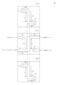
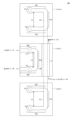
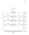
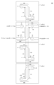
- the coupler disclosed herein is a coupled-line type coupler having a multi-layer structure in which multiple conductor layers are stacked, and includes a first line and a second line formed in different conductor layers, the first line being formed in multiple conductor layers sandwiching the conductor layer in which the second line is formed, and the first line and the second line at least partially overlap in the stacking direction of the conductor layers.
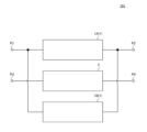
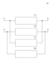
- FIG. 1 is an equivalent circuit diagram of a coupler according to an embodiment of the present disclosure.
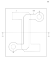
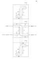
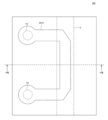
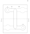
- FIG. 2 is a diagram illustrating a schematic configuration of a coupler according to an embodiment of the present disclosure.
- FIG. 3 is a diagram illustrating a schematic configuration of a coupler according to an embodiment of the present disclosure.
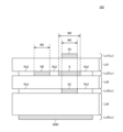
- FIG. 4 is a diagram illustrating a schematic configuration of a coupler according to an embodiment of the present disclosure.
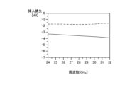
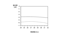
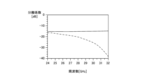
- FIG. 5 is a diagram illustrating a simulation result of the transmission characteristic of a coupler according to an embodiment of the present disclosure.
- FIG. 6 is a diagram illustrating a simulation result of the transmission characteristic of a coupler according to an embodiment of the present disclosure.
- FIG. 7 is a diagram illustrating a simulation result of the transmission characteristic of the coupler according to the embodiment of the present disclosure.
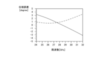
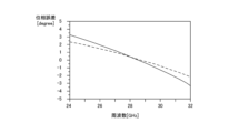
- FIG. 8 is a diagram illustrating a simulation result of the phase characteristic of the coupler according to the embodiment of the present disclosure.
- FIG. 9 is an equivalent circuit diagram of a coupler according to a first modification of the embodiment of the present disclosure.
- FIG. 10 is a diagram illustrating a schematic configuration of a coupler according to a first modification of the embodiment of the present disclosure.
- FIG. 11 is a diagram illustrating a schematic configuration of a coupler according to a first modification of the embodiment of the present disclosure.
- FIG. 12 is a diagram illustrating a schematic configuration of a coupler according to a first modification of the embodiment of the present disclosure.
- FIG. 13 is a diagram illustrating a simulation result of the phase characteristic of a coupler according to a modified example of an embodiment of the present disclosure.
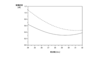
- FIG. 14 is a diagram illustrating a simulation result of the amplitude characteristic of a coupler according to a modified example of an embodiment of the present disclosure.
- FIG. 15 is an equivalent circuit diagram of a coupler according to a second modification of the embodiment of the present disclosure.
- FIG. 16 is a diagram illustrating a schematic configuration of a coupler according to a second modification of the embodiment of the present disclosure.
- FIG. 17 is a diagram illustrating a schematic configuration of a coupler according to a second modification of the embodiment of the present disclosure.
- FIG. 18 is a diagram illustrating a schematic configuration of a coupler according to a second modification of the embodiment of the present disclosure.
- FIG. 19 is an equivalent circuit diagram of a coupler according to a third modification of the embodiment of the present disclosure.
- FIG. 20 is a diagram illustrating a schematic configuration of a coupler according to a third modification of the embodiment of the present disclosure.
- FIG. 21 is a diagram illustrating a schematic configuration of a coupler according to a third modification of the embodiment of the present disclosure.
- FIG. 22 is a diagram illustrating a schematic configuration of a coupler according to a third modification of the embodiment of the present disclosure.
- FIG. 23 is a diagram illustrating a configuration of a transmission/reception device according to an embodiment of the present disclosure.
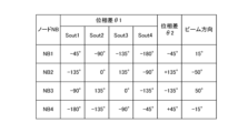
- FIG. 24 is a diagram illustrating an example of the beam direction of an RF signal transmitted by a transmission/reception device according to an embodiment of the present disclosure.
- branch-line hybrid couplers are often used as couplers that distribute signals equally, but the component size of branch-line hybrid couplers is large.
- the present disclosure has been made to solve the above-mentioned problems, and its purpose is to provide a coupler, a Butler matrix circuit, a transmission circuit, and a transmission device that can realize the miniaturization of electronic components equipped with couplers.
- coupler 101A outputs an RF signal Su based on an RF signal Sin received from each antenna 221 in a beam direction of -50° and amplified in each amplifier 211 to signal input/output unit 111 via isolation port P4 and switch 121.
- the transmission/reception circuit 301 is configured to include a bidirectional amplifier 211, but this is not limited to this.
- the transmission/reception circuit 301 may be configured to include a one-way amplifier for transmission and a one-way amplifier for reception that operate in a time division manner instead of the amplifier 211.
- the transmission/reception device 401 is described as being configured to transmit and receive RF signals, this is not limited thereto.
- the transmission/reception device 401 may be configured to transmit RF signals but not receive RF signals.
- the transmission/reception device 401 has a signal input unit that receives an analog signal from a signal processing unit (not shown) instead of the signal input/output unit 111.
- the transmission/reception device 401 may be configured to receive RF signals but not transmit RF signals.
- the transmission/reception device 401 has a signal output unit that outputs an analog signal to a signal processing unit (not shown) instead of the signal input/output unit 111.
- the transceiver circuit 301 is configured to transmit and receive RF signals, this is not limited thereto.
- the transceiver circuit 301 may be configured to transmit RF signals but not receive RF signals.
- the transceiver circuit 301 includes a one-way amplifier that amplifies the RF signal Sout, instead of the bidirectional amplifier 211.
- the transceiver circuit 301 may be configured to receive RF signals but not transmit RF signals.
- the transceiver circuit 301 includes a one-way amplifier that amplifies the RF signal Sin, instead of the bidirectional amplifier 211.
Landscapes
- Waveguides (AREA)
Abstract
Description
この出願は、2023年6月12日に出願された日本出願特願2023-95946号を基礎とする優先権を主張し、その開示のすべてをここに取り込む。
バトラーマトリクス回路およびドハティアンプ等の電子部品において、信号を等分配するカプラとして、ブランチライン型のハイブリッドカプラが用いられる場合が多い。しかしながら、ブランチライン型のハイブリッドカプラの場合、部品サイズが大きくなる。
本開示によれば、カプラを備える電子部品の小型化を実現することができる。
最初に、本開示の実施形態の内容を列記して説明する。
図1は、本開示の実施の形態に係るカプラの等価回路図である。図1を参照して、カプラ101は、主線路1である主線路1A,1Bと、副線路2と、入力ポートP1と、出力ポートP2と、結合ポートP3と、アイソレーションポートP4とを備える。入力ポートP1、出力ポートP2、結合ポートP3およびアイソレーションポートP4は、たとえば、端子であってもよいし、基板上のノードであってもよい。主線路1は、第1線路の一例である。副線路2は、第2線路の一例である。
図9は、本開示の実施の形態の変形例1に係るカプラの等価回路図である。図9を参照して、カプラ102は、カプラ101と比べて、主線路1の代わりに主線路3を備え、副線路2の代わりに副線路4である副線路4A,4Bを備える。主線路3は、第2線路の一例である。副線路4は、第1線路の一例である。
図15は、本開示の実施の形態の変形例2に係るカプラの等価回路図である。図15を参照して、カプラ103は、カプラ101と比べて、主線路1の代わりに主線路5である主線路5A,5B,5Cを備え、副線路2の代わりに副線路6を備える。主線路5は、第1線路の一例である。副線路6は、第2線路の一例である。
図19は、本開示の実施の形態の変形例3に係るカプラの等価回路図である。図19を参照して、カプラ104は、カプラ101と比べて、副線路2の代わりに副線路8である副線路8A,8Bを備える。副線路8は、第2線路の一例である。
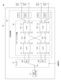
図23は、本開示の実施の形態に係る送受信装置の構成を示す図である。図23を参照して、送受信装置401は、信号入出力部111と、スイッチ121と、送受信回路301と、アンテナ221であるアンテナ221A,221B,221C,221Dとを備える。送受信装置401は、送信装置の一例である。アンテナ221A,221B,221C,221Dは、それぞれ、第1アンテナ、第2アンテナ、第3アンテナおよび第4アンテナの一例である。送受信装置401は、20GHz以上の周波数帯域のRF(Radio Freqency)信号のビームフォーミングに用いられる。
信号入出力部111は、図示しない信号処理部からアナログ信号を受けて、受けたアナログ信号に基づくRF信号Sdをスイッチ121経由でバトラーマトリクス回路201へ出力する。
アンテナ221は、RF信号Sinを受信し、受信したRF信号Sinを対応のアンプ211へ出力する。より詳細には、アンテナ221Aは、RF信号SinであるRF信号Sin1を受信してアンプ211Aへ出力する。また、アンテナ221Bは、RF信号SinであるRF信号Sin2を受信してアンプ211Bへ出力する。また、アンテナ221Cは、RF信号SinであるRF信号Sin3を受信してアンプ211Cへ出力する。また、アンテナ221Dは、RF信号SinであるRF信号Sin4を受信してアンプ211Dへ出力する。
[付記1]
20GHz以上の周波数帯域の信号の送信に用いられる送信回路であって、
同一の基板上に形成され、かつ複数の導電体層が積層された多層構成を有する結合線路型のカプラを複数備える、バトラーマトリクス回路と、
前記基板に搭載された複数のアンプとを備え、
前記カプラは、互いに異なる前記導電体層に形成された第1線路および第2線路を備え、前記第1線路は、前記第2線路が形成された前記導電体層を間に挟む複数の前記導電体層に亘って形成され、前記第1線路および前記第2線路は、前記導電体層の積層方向において少なくとも一部が重なっており、
前記カプラは、入力ポート、出力ポート、結合ポートおよびアイソレーションポートを含み、
第1の前記カプラの前記結合ポートが第3の前記カプラの前記入力ポートに接続され、
第2の前記カプラの前記結合ポートが前記第3のカプラの前記アイソレーションポートに接続され、
前記第1のカプラの前記出力ポートが第4の前記カプラの前記入力ポートに接続され、
前記第2のカプラの前記出力ポートが前記第4のカプラの前記アイソレーションポートに接続され、
前記複数のアンプは、前記第3のカプラの前記結合ポートから出力される信号を増幅する第1アンプと、前記第3のカプラの前記出力ポートから出力される信号を増幅する第2アンプと、前記第4のカプラの前記結合ポートから出力される信号を増幅する第3アンプと、前記第4のカプラの前記出力ポートから出力される信号を増幅する第4アンプとを含み、
前記複数のアンプは、GaNトランジスタを用いて構成される、送信回路。
2,4,4A,4B,6,8,8A,8B 副線路
11A,11B,21,31,41A,41B,51A,51B,51C,81A,81B 結合部分
12A,12B,13A,13B,22,23,32,33,42A,42B,43A,43B,52A,52B,52C,53A,53B,53C,82A,82B,83A,83B 配線部分
101,101A,101B,101C,101D,102,103,104 カプラ
111 信号入出力部
121 スイッチ
151A,151B 移相器
201 バトラーマトリクス回路
211,211A,211B,211C,211D アンプ
221,221A,221B,221C,221D アンテナ
251 基板
301 送受信回路
401 送受信装置
P1 入力ポート
P2 出力ポート
P3 結合ポート
P4 アイソレーションポート
V1,V2,V3,V4,V5,V6,V9,V10 ビア
Lc,Lc1,Lc2,Lc3,Lc4,Lc5 導電体層
Ld1,Ld2,Ld3,Ld4 誘電体層
Rs2,Rs3,Rs5 樹脂
GND グランドパターン
NA,NB,NB1,NB2,NB3,NB4 ノード
Claims (7)
- 複数の導電体層が積層された多層構成を有する結合線路型のカプラであって、
互いに異なる前記導電体層に形成された第1線路および第2線路を備え、
前記第1線路は、前記第2線路が形成された前記導電体層を間に挟む複数の前記導電体層に形成され、
前記第1線路および前記第2線路は、前記導電体層の積層方向において少なくとも一部が重なっている、カプラ。 - 前記第1線路は、第1端が前記カプラにおける入力ポートに接続され、かつ第2端が前記カプラにおける出力ポートに接続され、
前記第2線路は、第1端が前記カプラにおける結合ポートに接続され、かつ第2端が前記カプラにおけるアイソレーションポートに接続されている、請求項1に記載のカプラ。 - 前記第1線路は、前記第2線路が形成された前記導電体層にさらに形成される、請求項1または請求項2に記載のカプラ。
- 同一の基板上に形成され、かつ複数の導電体層が積層された多層構成を有する結合線路型のカプラを複数備え、
前記カプラは、互いに異なる前記導電体層に形成された第1線路および第2線路を備え、前記第1線路は、前記第2線路が形成された前記導電体層を間に挟む複数の前記導電体層に亘って形成され、前記第1線路および前記第2線路は、前記導電体層の積層方向において少なくとも一部が重なっており、
前記カプラは、入力ポート、出力ポート、結合ポートおよびアイソレーションポートを含み、
第1の前記カプラの前記結合ポートが第3の前記カプラの前記入力ポートに接続され、
第2の前記カプラの前記結合ポートが前記第3のカプラの前記アイソレーションポートに接続され、
前記第1のカプラの前記出力ポートが第4の前記カプラの前記入力ポートに接続され、
前記第2のカプラの前記出力ポートが前記第4のカプラの前記アイソレーションポートに接続されている、バトラーマトリクス回路。 - 前記第1線路および前記第2線路は、前記導電体層の積層方向において交差している、請求項4に記載のバトラーマトリクス回路。
- 20GHz以上の周波数帯域の信号の送信に用いられる送信回路であって、
請求項4または請求項5に記載のバトラーマトリクス回路と、
前記基板に搭載された複数のアンプとを備え、
前記複数のアンプは、前記第3のカプラの前記結合ポートから出力される信号を増幅する第1アンプと、前記第3のカプラの前記出力ポートから出力される信号を増幅する第2アンプと、前記第4のカプラの前記結合ポートから出力される信号を増幅する第3アンプと、前記第4のカプラの前記出力ポートから出力される信号を増幅する第4アンプとを含む、送信回路。 - ビームフォーミングに用いられる送信装置であって、
請求項6に記載の送信回路と、
複数のアンテナとを備え、
前記複数のアンテナは、前記第1アンプにより増幅された信号を送信する第1アンテナと、前記第2アンプにより増幅された信号を送信する第2アンテナと、前記第3アンプにより増幅された信号を送信する第3アンテナと、前記第4アンプにより増幅された信号を送信する第4アンテナとを含む、送信装置。
Priority Applications (2)
| Application Number | Priority Date | Filing Date | Title |
|---|---|---|---|
| JP2025527535A JPWO2024257500A1 (ja) | 2023-06-12 | 2024-04-30 | |
| CN202480034441.5A CN121175870A (zh) | 2023-06-12 | 2024-04-30 | 耦合器、巴特勒矩阵电路、发送电路及发送装置 |
Applications Claiming Priority (2)
| Application Number | Priority Date | Filing Date | Title |
|---|---|---|---|
| JP2023-095946 | 2023-06-12 | ||
| JP2023095946 | 2023-06-12 |
Publications (1)
| Publication Number | Publication Date |
|---|---|
| WO2024257500A1 true WO2024257500A1 (ja) | 2024-12-19 |
Family
ID=93851961
Family Applications (1)
| Application Number | Title | Priority Date | Filing Date |
|---|---|---|---|
| PCT/JP2024/016624 Ceased WO2024257500A1 (ja) | 2023-06-12 | 2024-04-30 | カプラ、バトラーマトリクス回路、送信回路および送信装置 |
Country Status (3)
| Country | Link |
|---|---|
| JP (1) | JPWO2024257500A1 (ja) |
| CN (1) | CN121175870A (ja) |
| WO (1) | WO2024257500A1 (ja) |
Citations (3)
| Publication number | Priority date | Publication date | Assignee | Title |
|---|---|---|---|---|
| WO2019116648A1 (ja) * | 2017-12-11 | 2019-06-20 | ソニーセミコンダクタソリューションズ株式会社 | バトラーマトリクス回路、フェーズドアレイアンテナ、フロントエンドモジュール及び無線通信端末 |
| WO2019189228A1 (ja) * | 2018-03-29 | 2019-10-03 | 株式会社村田製作所 | 方向性結合器 |
| WO2022080089A1 (ja) * | 2020-10-12 | 2022-04-21 | 株式会社村田製作所 | 方向性結合器 |
-
2024
- 2024-04-30 WO PCT/JP2024/016624 patent/WO2024257500A1/ja not_active Ceased
- 2024-04-30 JP JP2025527535A patent/JPWO2024257500A1/ja active Pending
- 2024-04-30 CN CN202480034441.5A patent/CN121175870A/zh active Pending
Patent Citations (3)
| Publication number | Priority date | Publication date | Assignee | Title |
|---|---|---|---|---|
| WO2019116648A1 (ja) * | 2017-12-11 | 2019-06-20 | ソニーセミコンダクタソリューションズ株式会社 | バトラーマトリクス回路、フェーズドアレイアンテナ、フロントエンドモジュール及び無線通信端末 |
| WO2019189228A1 (ja) * | 2018-03-29 | 2019-10-03 | 株式会社村田製作所 | 方向性結合器 |
| WO2022080089A1 (ja) * | 2020-10-12 | 2022-04-21 | 株式会社村田製作所 | 方向性結合器 |
Non-Patent Citations (1)
| Title |
|---|
| KUO, CHECHUNG ET AL.: "A Fully SiP Integrated V-Band Butler Matrix End-Fire Beam- Switching Transmitter Using Flip-Chip Assembled CMOS Chips on LTCC", IEEE TRANSACTIONS ON MICROWAVE THEORY AND TECHNIQUES, vol. 60, no. 5, May 2012 (2012-05-01), pages 1424 - 1436, XP011442422, Retrieved from the Internet <URL:https://ieeexplore.ieee.org/abstract/document/6172540> [retrieved on 20240627], DOI: 10.1109/TMTT.2012.2187795 * |
Also Published As
| Publication number | Publication date |
|---|---|
| JPWO2024257500A1 (ja) | 2024-12-19 |
| CN121175870A (zh) | 2025-12-19 |
Similar Documents
| Publication | Publication Date | Title |
|---|---|---|
| US11631933B2 (en) | Antenna module and communication device | |
| CN102273005B (zh) | 整合式毫米波移相器及其方法 | |
| EP0511728B1 (en) | Coplanar waveguide directional coupler and flip-chip microwave monolithic integrated circuit assembly incorporating the coupler | |
| US8013784B2 (en) | Butler matrix for 3D integrated RF front-ends | |
| US10461393B2 (en) | Bidirectional coupler, monitor circuit, and front-end circuit | |
| WO2019026595A1 (ja) | アンテナモジュールおよび通信装置 | |
| US11870164B2 (en) | Antenna module and communication device equipped with the same | |
| CN112582770B (zh) | 定向耦合器及电子部件模块 | |
| JP7524478B2 (ja) | 複数の表面境界を有するビームフォーマicチップ付き集積アンテナアレイ | |
| US20160087823A1 (en) | Non-reciprocal components with balanced distributedly modulated capacitors (dmc) | |
| KR20210103400A (ko) | 고주파 모듈 및 통신 장치 | |
| JP2019087832A (ja) | 双方向型方向性結合器 | |
| US12347917B2 (en) | Directional coupler | |
| JP2021129172A (ja) | インピーダンス変換器及び電子装置 | |
| WO2022209727A1 (ja) | 高周波モジュールおよび通信装置 | |
| KR100951552B1 (ko) | 방향성 결합기 및 이를 포함하는 듀플렉스 송수신 시스템의시스템 인 패키지 | |
| CN121175870A (zh) | 耦合器、巴特勒矩阵电路、发送电路及发送装置 | |
| WO2022107460A1 (ja) | 高周波モジュールおよび通信装置 | |
| US12537511B2 (en) | Radio-frequency module and communication device | |
| US12542342B2 (en) | Directional coupler | |
| WO2018212238A1 (ja) | 方向性結合器および通信装置 | |
| US20230007765A1 (en) | Circuit structure | |
| WO2022209757A1 (ja) | 高周波モジュールおよび通信装置 | |
| KR20230154890A (ko) | Rf 구성 요소 사이에 동일 평면 도파관 상호연결부를 사용하는 안테나 장치 | |
| KR102603211B1 (ko) | 다층 구조 위상 천이기 |
Legal Events
| Date | Code | Title | Description |
|---|---|---|---|
| 121 | Ep: the epo has been informed by wipo that ep was designated in this application |
Ref document number: 24823122 Country of ref document: EP Kind code of ref document: A1 |
|
| ENP | Entry into the national phase |
Ref document number: 2025527535 Country of ref document: JP Kind code of ref document: A |
|
| WWE | Wipo information: entry into national phase |
Ref document number: 2025527535 Country of ref document: JP |
|
| NENP | Non-entry into the national phase |
Ref country code: DE |
|
| 122 | Ep: pct application non-entry in european phase |
Ref document number: 24823122 Country of ref document: EP Kind code of ref document: A1 |