WO2024252853A1 - 照明装置 - Google Patents
照明装置 Download PDFInfo
- Publication number
- WO2024252853A1 WO2024252853A1 PCT/JP2024/017590 JP2024017590W WO2024252853A1 WO 2024252853 A1 WO2024252853 A1 WO 2024252853A1 JP 2024017590 W JP2024017590 W JP 2024017590W WO 2024252853 A1 WO2024252853 A1 WO 2024252853A1
- Authority
- WO
- WIPO (PCT)
- Prior art keywords
- optical element
- signal
- pulse wave
- input
- liquid crystal
- Prior art date
- Legal status (The legal status is an assumption and is not a legal conclusion. Google has not performed a legal analysis and makes no representation as to the accuracy of the status listed.)
- Ceased
Links
Images




Classifications
-
- G—PHYSICS
- G02—OPTICS
- G02F—OPTICAL DEVICES OR ARRANGEMENTS FOR THE CONTROL OF LIGHT BY MODIFICATION OF THE OPTICAL PROPERTIES OF THE MEDIA OF THE ELEMENTS INVOLVED THEREIN; NON-LINEAR OPTICS; FREQUENCY-CHANGING OF LIGHT; OPTICAL LOGIC ELEMENTS; OPTICAL ANALOGUE/DIGITAL CONVERTERS
- G02F1/00—Devices or arrangements for the control of the intensity, colour, phase, polarisation or direction of light arriving from an independent light source, e.g. switching, gating or modulating; Non-linear optics
- G02F1/01—Devices or arrangements for the control of the intensity, colour, phase, polarisation or direction of light arriving from an independent light source, e.g. switching, gating or modulating; Non-linear optics for the control of the intensity, phase, polarisation or colour
- G02F1/13—Devices or arrangements for the control of the intensity, colour, phase, polarisation or direction of light arriving from an independent light source, e.g. switching, gating or modulating; Non-linear optics for the control of the intensity, phase, polarisation or colour based on liquid crystals, e.g. single liquid crystal display cells
- G02F1/133—Constructional arrangements; Operation of liquid crystal cells; Circuit arrangements
- G02F1/1333—Constructional arrangements; Manufacturing methods
- G02F1/1347—Arrangement of liquid crystal layers or cells in which the final condition of one light beam is achieved by the addition of the effects of two or more layers or cells
-
- F—MECHANICAL ENGINEERING; LIGHTING; HEATING; WEAPONS; BLASTING
- F21—LIGHTING
- F21L—LIGHTING DEVICES OR SYSTEMS THEREOF, BEING PORTABLE OR SPECIALLY ADAPTED FOR TRANSPORTATION
- F21L4/00—Electric lighting devices with self-contained electric batteries or cells
-
- F—MECHANICAL ENGINEERING; LIGHTING; HEATING; WEAPONS; BLASTING
- F21—LIGHTING
- F21L—LIGHTING DEVICES OR SYSTEMS THEREOF, BEING PORTABLE OR SPECIALLY ADAPTED FOR TRANSPORTATION
- F21L4/00—Electric lighting devices with self-contained electric batteries or cells
- F21L4/04—Electric lighting devices with self-contained electric batteries or cells characterised by the provision of a light source housing portion adjustably fixed to the remainder of the device
-
- F—MECHANICAL ENGINEERING; LIGHTING; HEATING; WEAPONS; BLASTING
- F21—LIGHTING
- F21V—FUNCTIONAL FEATURES OR DETAILS OF LIGHTING DEVICES OR SYSTEMS THEREOF; STRUCTURAL COMBINATIONS OF LIGHTING DEVICES WITH OTHER ARTICLES, NOT OTHERWISE PROVIDED FOR
- F21V14/00—Controlling the distribution of the light emitted by adjustment of elements
-
- F—MECHANICAL ENGINEERING; LIGHTING; HEATING; WEAPONS; BLASTING
- F21—LIGHTING
- F21V—FUNCTIONAL FEATURES OR DETAILS OF LIGHTING DEVICES OR SYSTEMS THEREOF; STRUCTURAL COMBINATIONS OF LIGHTING DEVICES WITH OTHER ARTICLES, NOT OTHERWISE PROVIDED FOR
- F21V14/00—Controlling the distribution of the light emitted by adjustment of elements
- F21V14/003—Controlling the distribution of the light emitted by adjustment of elements by interposition of elements with electrically controlled variable light transmissivity, e.g. liquid crystal elements or electrochromic devices
-
- F—MECHANICAL ENGINEERING; LIGHTING; HEATING; WEAPONS; BLASTING
- F21—LIGHTING
- F21V—FUNCTIONAL FEATURES OR DETAILS OF LIGHTING DEVICES OR SYSTEMS THEREOF; STRUCTURAL COMBINATIONS OF LIGHTING DEVICES WITH OTHER ARTICLES, NOT OTHERWISE PROVIDED FOR
- F21V23/00—Arrangement of electric circuit elements in or on lighting devices
- F21V23/04—Arrangement of electric circuit elements in or on lighting devices the elements being switches
-
- F—MECHANICAL ENGINEERING; LIGHTING; HEATING; WEAPONS; BLASTING
- F21—LIGHTING
- F21V—FUNCTIONAL FEATURES OR DETAILS OF LIGHTING DEVICES OR SYSTEMS THEREOF; STRUCTURAL COMBINATIONS OF LIGHTING DEVICES WITH OTHER ARTICLES, NOT OTHERWISE PROVIDED FOR
- F21V5/00—Refractors for light sources
-
- G—PHYSICS
- G02—OPTICS
- G02F—OPTICAL DEVICES OR ARRANGEMENTS FOR THE CONTROL OF LIGHT BY MODIFICATION OF THE OPTICAL PROPERTIES OF THE MEDIA OF THE ELEMENTS INVOLVED THEREIN; NON-LINEAR OPTICS; FREQUENCY-CHANGING OF LIGHT; OPTICAL LOGIC ELEMENTS; OPTICAL ANALOGUE/DIGITAL CONVERTERS
- G02F1/00—Devices or arrangements for the control of the intensity, colour, phase, polarisation or direction of light arriving from an independent light source, e.g. switching, gating or modulating; Non-linear optics
- G02F1/01—Devices or arrangements for the control of the intensity, colour, phase, polarisation or direction of light arriving from an independent light source, e.g. switching, gating or modulating; Non-linear optics for the control of the intensity, phase, polarisation or colour
- G02F1/13—Devices or arrangements for the control of the intensity, colour, phase, polarisation or direction of light arriving from an independent light source, e.g. switching, gating or modulating; Non-linear optics for the control of the intensity, phase, polarisation or colour based on liquid crystals, e.g. single liquid crystal display cells
-
- G—PHYSICS
- G02—OPTICS
- G02F—OPTICAL DEVICES OR ARRANGEMENTS FOR THE CONTROL OF LIGHT BY MODIFICATION OF THE OPTICAL PROPERTIES OF THE MEDIA OF THE ELEMENTS INVOLVED THEREIN; NON-LINEAR OPTICS; FREQUENCY-CHANGING OF LIGHT; OPTICAL LOGIC ELEMENTS; OPTICAL ANALOGUE/DIGITAL CONVERTERS
- G02F1/00—Devices or arrangements for the control of the intensity, colour, phase, polarisation or direction of light arriving from an independent light source, e.g. switching, gating or modulating; Non-linear optics
- G02F1/01—Devices or arrangements for the control of the intensity, colour, phase, polarisation or direction of light arriving from an independent light source, e.g. switching, gating or modulating; Non-linear optics for the control of the intensity, phase, polarisation or colour
- G02F1/13—Devices or arrangements for the control of the intensity, colour, phase, polarisation or direction of light arriving from an independent light source, e.g. switching, gating or modulating; Non-linear optics for the control of the intensity, phase, polarisation or colour based on liquid crystals, e.g. single liquid crystal display cells
- G02F1/133—Constructional arrangements; Operation of liquid crystal cells; Circuit arrangements
-
- G—PHYSICS
- G02—OPTICS
- G02F—OPTICAL DEVICES OR ARRANGEMENTS FOR THE CONTROL OF LIGHT BY MODIFICATION OF THE OPTICAL PROPERTIES OF THE MEDIA OF THE ELEMENTS INVOLVED THEREIN; NON-LINEAR OPTICS; FREQUENCY-CHANGING OF LIGHT; OPTICAL LOGIC ELEMENTS; OPTICAL ANALOGUE/DIGITAL CONVERTERS
- G02F1/00—Devices or arrangements for the control of the intensity, colour, phase, polarisation or direction of light arriving from an independent light source, e.g. switching, gating or modulating; Non-linear optics
- G02F1/01—Devices or arrangements for the control of the intensity, colour, phase, polarisation or direction of light arriving from an independent light source, e.g. switching, gating or modulating; Non-linear optics for the control of the intensity, phase, polarisation or colour
- G02F1/13—Devices or arrangements for the control of the intensity, colour, phase, polarisation or direction of light arriving from an independent light source, e.g. switching, gating or modulating; Non-linear optics for the control of the intensity, phase, polarisation or colour based on liquid crystals, e.g. single liquid crystal display cells
- G02F1/133—Constructional arrangements; Operation of liquid crystal cells; Circuit arrangements
- G02F1/13306—Circuit arrangements or driving methods for the control of single liquid crystal cells
-
- G—PHYSICS
- G02—OPTICS
- G02F—OPTICAL DEVICES OR ARRANGEMENTS FOR THE CONTROL OF LIGHT BY MODIFICATION OF THE OPTICAL PROPERTIES OF THE MEDIA OF THE ELEMENTS INVOLVED THEREIN; NON-LINEAR OPTICS; FREQUENCY-CHANGING OF LIGHT; OPTICAL LOGIC ELEMENTS; OPTICAL ANALOGUE/DIGITAL CONVERTERS
- G02F1/00—Devices or arrangements for the control of the intensity, colour, phase, polarisation or direction of light arriving from an independent light source, e.g. switching, gating or modulating; Non-linear optics
- G02F1/01—Devices or arrangements for the control of the intensity, colour, phase, polarisation or direction of light arriving from an independent light source, e.g. switching, gating or modulating; Non-linear optics for the control of the intensity, phase, polarisation or colour
- G02F1/13—Devices or arrangements for the control of the intensity, colour, phase, polarisation or direction of light arriving from an independent light source, e.g. switching, gating or modulating; Non-linear optics for the control of the intensity, phase, polarisation or colour based on liquid crystals, e.g. single liquid crystal display cells
- G02F1/133—Constructional arrangements; Operation of liquid crystal cells; Circuit arrangements
- G02F1/1333—Constructional arrangements; Manufacturing methods
- G02F1/1335—Structural association of cells with optical devices, e.g. polarisers or reflectors
- G02F1/1336—Illuminating devices
- G02F1/133602—Direct backlight
- G02F1/133612—Electrical details
-
- G—PHYSICS
- G02—OPTICS
- G02F—OPTICAL DEVICES OR ARRANGEMENTS FOR THE CONTROL OF LIGHT BY MODIFICATION OF THE OPTICAL PROPERTIES OF THE MEDIA OF THE ELEMENTS INVOLVED THEREIN; NON-LINEAR OPTICS; FREQUENCY-CHANGING OF LIGHT; OPTICAL LOGIC ELEMENTS; OPTICAL ANALOGUE/DIGITAL CONVERTERS
- G02F1/00—Devices or arrangements for the control of the intensity, colour, phase, polarisation or direction of light arriving from an independent light source, e.g. switching, gating or modulating; Non-linear optics
- G02F1/01—Devices or arrangements for the control of the intensity, colour, phase, polarisation or direction of light arriving from an independent light source, e.g. switching, gating or modulating; Non-linear optics for the control of the intensity, phase, polarisation or colour
- G02F1/13—Devices or arrangements for the control of the intensity, colour, phase, polarisation or direction of light arriving from an independent light source, e.g. switching, gating or modulating; Non-linear optics for the control of the intensity, phase, polarisation or colour based on liquid crystals, e.g. single liquid crystal display cells
- G02F1/133—Constructional arrangements; Operation of liquid crystal cells; Circuit arrangements
- G02F1/1333—Constructional arrangements; Manufacturing methods
- G02F1/1343—Electrodes
- G02F1/134309—Electrodes characterised by their geometrical arrangement
Definitions
- One embodiment of the present invention relates to a lighting device that uses liquid crystal to control the distribution of light emitted from a light source.
- liquid crystal lenses optical elements that utilize the change in refractive index of liquid crystals by adjusting the voltage applied to the liquid crystal, known as liquid crystal lenses.
- development of lighting devices that use light sources and liquid crystal lenses is underway (see, for example, Patent Document 1).
- the spread of light emitted from the lighting device i.e., the light distribution angle
- the optical element such as a liquid crystal lens
- Such lighting devices are not only used by installing them in a predetermined position, but also by users carrying them around. When a user uses the lighting device while holding it, it is preferable that the light distribution angle can be easily adjusted while the user is holding the lighting device.
- One of the objects of one embodiment of the present invention is to provide a lighting device that can easily adjust the light distribution angle. Also, one of the objects of one embodiment of the present invention is to provide a lighting device that can easily adjust the light distribution shape.
- the lighting device includes a light source, an optical element including a first liquid crystal cell that transmits light emitted from the light source in a diffusible manner, an optical element driving circuit unit connected to the optical element and generating a signal for driving the optical element, and a first push switch including a push button operated by a user and connected to the optical element driving circuit unit,
- the first liquid crystal cell includes a first substrate on which first transparent electrodes and second transparent electrodes extending in a first direction are alternately provided, a second substrate on which third transparent electrodes and fourth transparent electrodes extending in a second direction intersecting the first direction are alternately provided, and a liquid crystal layer between the first substrate and the second substrate
- the optical element driving circuit unit is electrically connected to a plurality of input side contacts of the first push switch.
- the optical element includes a first resistor voltage divider circuit, a first output terminal electrically connected to the output contact of the first push switch and outputting a first signal having a first pulse wave, and a second output terminal electrically connected to the output contact of the first push switch and outputting a second signal having a second pulse wave in which the phase of the first pulse wave is inverted.
- the first signal is input to the optical element so that the first pulse wave is applied to the first transparent electrode
- the second signal is input to the optical element so that the second pulse wave is applied to the second transparent electrode.
- the lighting device includes a light source, an optical element including a first liquid crystal cell that transmits light emitted from the light source in a diffusible manner, an optical element driving circuit connected to the optical element and generating a signal for driving the optical element, a first push switch including a first push button operated by a user and connected to the optical element driving circuit, and a second push switch including a second push button operated by a user, the first input side contact, the second input side contact, the third input side contact, and the fourth input side contact being electrically connected to the optical element driving circuit, and the first output side contact and the second output side contact being electrically connected to the optical element, and the first liquid crystal cell includes a first substrate on which first transparent electrodes and second transparent electrodes extending in a first direction are alternately provided, a second substrate on which third transparent electrodes and fourth transparent electrodes extending in a second direction intersecting the first direction are alternately provided, and a first substrate and a second substrate on which third transparent electrodes and fourth transparent electrodes
- the optical element driving circuit generates a first signal having a first pulse wave, a second signal having an inverted phase of the first pulse wave, and a third signal having a fixed potential
- the first signal and the second signal are input to the first input contact and the second input contact of the second push switch, respectively
- the third signal is input to the third input contact and the fourth input contact of the second push switch
- each time the second push button of the second push switch is pressed one of the first input contact and the second input contact electrically connected to the first output contact is selected, and one of the third input contact and the fourth input contact electrically connected to the second output contact is selected, and the first pulse wave and the second pulse wave are applied to the first transparent electrode and the second transparent electrode, respectively, or a fixed potential is applied to the first transparent electrode and the second transparent electrode.
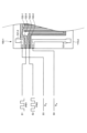
- 1 is a schematic side view showing a configuration of an illumination device according to an embodiment of the present invention.
- 1 is a schematic top view showing a configuration of an illumination device according to an embodiment of the present invention.
- 1 is a schematic block diagram showing an internal configuration of a lighting device according to an embodiment of the present invention;
- 1 is a schematic cross-sectional view showing a configuration of an optical element of an illumination device according to one embodiment of the present invention.
- 1 is a schematic cross-sectional view showing a configuration of an optical element of an illumination device according to one embodiment of the present invention.
- 2 is a schematic plan view showing an electrode pattern of a liquid crystal cell included in an optical element of an illumination device according to one embodiment of the present invention.
- FIG. 2 is a schematic plan view showing an electrode pattern of a liquid crystal cell included in an optical element of an illumination device according to one embodiment of the present invention.
- FIG. 5A and 5B are schematic diagrams illustrating optical characteristics of a liquid crystal cell included in an optical element of an illumination device according to one embodiment of the present invention.
- 5A and 5B are schematic diagrams illustrating optical characteristics of a liquid crystal cell included in an optical element of an illumination device according to one embodiment of the present invention.
- 2 is a block diagram showing a circuit configuration of an optical element driving circuit section of an illumination device according to an embodiment of the present invention.
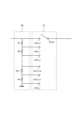
- FIG. 1 is a circuit diagram showing a circuit configuration of a push switch and a resistive voltage divider circuit included in an optical element driving circuit section of an illumination device according to an embodiment of the present invention.
- FIG. 4 is a schematic diagram showing a signal input to an optical element of an illumination device according to one embodiment of the present invention.
- FIG. 2 is a block diagram showing a circuit configuration of an optical element driving circuit section of an illumination device according to an embodiment of the present invention.
- FIG. 2 is a block diagram showing a circuit configuration of an optical element driving circuit section of an illumination device according to an embodiment of the present invention.
- FIG. 1 is a schematic block diagram showing an internal configuration of a lighting device according to an embodiment of the present invention; 4 is a schematic diagram showing a signal input to an optical element of an illumination device according to one embodiment of the present invention.
- drawings may show the width, thickness, shape, etc. of each part in a schematic manner compared to the actual embodiment, but these are merely examples, and the illustrated shapes themselves do not limit the interpretation of the present invention.
- components with the same functions as those explained in relation to previous drawings in the specification may be given the same reference numerals even in separate drawings, and duplicate explanations may be omitted.
- each structure When a film is processed to form multiple structures, each structure may have a different function or role, and each structure may be formed on a different base.
- these multiple structures originate from a film formed as the same layer in the same process, and are made of the same material. Therefore, these multiple films are defined as existing in the same layer.
- FIG. 1A First Embodiment An illumination device 1 according to an embodiment of the present invention will be described with reference to FIGS. 1A to 7.
- FIG. 1A First Embodiment An illumination device 1 according to an embodiment of the present invention will be described with reference to FIGS. 1A to 7.
- FIG. 1A First Embodiment An illumination device 1 according to an embodiment of the present invention will be described with reference to FIGS. 1A to 7.
- Configuration of lighting device 1] 1A and 1B are schematic side and top views, respectively, illustrating the configuration of an illumination device 1 according to one embodiment of the present invention.
- the lighting device 1 includes a main body 1a and a lighting unit 1b.
- the lighting unit 1b is connected to an end of the main body 1a.
- the main body 1a has a cylindrical shape, and light is emitted from the lighting unit 1b. While holding the main body 1a, the user can illuminate the surroundings of the user with the light emitted from the lighting unit 1b. In this way, the lighting device 1 can be used as a flashlight. However, the usage of the lighting device 1 is not limited to this.
- the lighting device 1 can also be used as a spotlight.
- the direction in which the main body 1a extends is defined as the z-axis direction when viewed from above.
- the emission direction of the light emitted from the illumination unit 1b is the z-axis direction.
- the direction perpendicular to the z-axis direction is defined as the x-axis direction.
- the diffusion direction of the light emitted from the illumination unit 1b is the x-axis direction.
- the direction perpendicular to the z-axis and x-axis directions is defined as the y-axis direction.
- the main body 1a has a curved shape. Specifically, the main body 1a extends parallel to the z-axis direction and has a shape in which a portion parallel to the z-axis direction that is connected to the lighting unit 1b is combined with a portion extending in a direction not parallel to the z-axis direction.
- the main body 1a has such a shape, even when the user uses the lighting device 1 close to the user's face, the user can hold the main body 1a without applying excessive force to the user's wrist to illuminate the user's surroundings.
- the shape of the main body 1a is not limited to this.
- the shape of the main body 1a can be a shape that corresponds to the usage manner of the lighting device 1.
- the upper surface of the main body 1a is provided with a push button for a push switch 61.
- the push switch 61 adjusts the light distribution angle of the light emitted from the lighting unit 1b. That is, when the user presses the push button for the push switch 61, the light distribution angle of the light emitted from the lighting unit 1b changes in stages.
- the main body 1a also includes a light source adjustment switch 71 that adjusts the brightness of the light emitted from the lighting unit 1b.
- a knob for a slide switch or a push button for a push switch may be provided on the side of the main body 1a.
- the light source adjustment switch 71 is a slide switch, the brightness of the light emitted from the lighting unit 1b can be continuously adjusted by sliding the knob.
- the light source adjustment switch 71 is a push switch, the brightness of the light emitted from the lighting unit 1b can be adjusted in stages by pressing the push button for the push switch.
- FIG. 1C is a schematic block diagram showing the internal configuration of a lighting device 1 according to one embodiment of the present invention.
- the lighting device 1 includes an optical element 10, a light source 20, an optical adjustment unit 30, a battery 40, a charging module 50, an optical element drive circuit unit 60, and a light source drive circuit unit 70.
- the optical element 10, the light source 20, and the optical adjustment unit 30 are housed in the lighting unit 1b.
- the battery 40, the charging module 50, the optical element drive circuit unit 60, and the light source drive circuit unit 70 are housed in the main body unit 1a.
- FIG. 1C shows the connections between the components.
- the optical element drive circuit unit 60 is connected to the optical element 10 and the battery 40.
- the optical element drive circuit unit 60 receives power from the battery 40, and generates a signal to drive the optical element 10.
- the optical element drive circuit unit 60 is also connected to a push switch 61.
- the light source drive circuit unit 70 is connected to the light source 20 and the battery 40.
- the light source drive circuit unit 70 receives power from the battery 40, and generates a signal to drive the light source 20.
- the light source drive circuit unit 70 is also connected to a light source adjustment switch 71.
- the battery 40 is connected to the charging module 50.
- the battery 40 can be a so-called secondary battery (e.g., lithium ion battery, etc.) that can be used repeatedly by charging.
- the battery 40 can be charged via the charging module 50.
- the charging module 50 controls the charging of the battery 40 while preventing overcharging of the battery 40.
- the battery 40 can be charged in a wired or wireless configuration. In a wired configuration, the charging module 50 is provided with a terminal for connecting a power cable, and power is charged to the battery 40 via the power cable connected to the terminal of the charging module 50. In a wireless configuration, a power receiving coil is provided in the charging module 50, and the power converted by the power receiving coil is charged to the battery 40.
- a configuration in which the charging module 50 is not provided can also be applied to the lighting device 1.
- a so-called primary battery e.g., alkaline dry battery or manganese dry battery, etc.
- the battery 40 can be used as the battery 40.
- the light source 20 emits light to the optical element 10.
- a light emitting diode LED
- a plurality of LEDs may be used as the light source 20.
- LEDs of the same color may be used, or LEDs of different colors may be used.
- the light source 20 is not limited to an LED.
- the light source 20 may be any element or device that can emit light.
- the optical adjustment unit 30 is disposed between the optical element 10 and the light source 20, and converges, diffuses, or reflects the light emitted from the light source 20.
- the optical adjustment unit 30 is an optical component that is a lens or a reflector, or a combination of these.
- FIG. 2A and 2B are schematic cross-sectional views showing a configuration of an optical element 10 of an illumination device 1 according to an embodiment of the present invention.
- Fig. 2A is a cross-sectional view of the optical element 10 cut along a plane perpendicular to the y-axis direction
- Fig. 2B is a cross-sectional view of the optical element 10 cut along a plane perpendicular to the x-axis direction.
- the optical element 10 includes four liquid crystal cells 100 (first liquid crystal cell 100-1, second liquid crystal cell 100-2, third liquid crystal cell 100-3, and fourth liquid crystal cell 100-4).
- the first liquid crystal cell 100-1, second liquid crystal cell 100-2, third liquid crystal cell 100-3, and fourth liquid crystal cell 100-4 are stacked in order in the z-axis direction from the side closest to the light source 20.
- Light emitted from the light source 20 is incident on the first liquid crystal cell 100-1 and is emitted from the fourth liquid crystal cell 100-4.
- the diffusion and polarization of light are controlled by the four liquid crystal cells 100 included in the optical element 10, and the light distribution of the light emitted from the fourth liquid crystal cell 100-4 can be changed. That is, the optical element 10 transmits the light emitted from the light source 20 in a diffusible manner and can control the light distribution.
- FIGS 2A and 2B show the configuration of an optical element 10 including four liquid crystal cells 100, but the number of liquid crystal cells 100 included in the optical element 10 is not limited to four. It is sufficient that the optical element 10 includes at least one liquid crystal cell 100.
- each of the first liquid crystal cell 100-1 to the fourth liquid crystal cell 100-4 includes a first substrate 110-1, a second substrate 110-2, a plurality of first transparent electrodes 120-1, a plurality of second transparent electrodes 120-2, a plurality of third transparent electrodes 120-3, a plurality of fourth transparent electrodes 120-4, a first alignment film 130-1, a second alignment film 130-2, a sealant 140, and a liquid crystal layer 150.
- the first transparent electrodes 120-1 and the second transparent electrodes 120-2 are alternately provided on the first substrate 110-1.
- a first alignment film 130-1 is provided on the first substrate 110-1 so as to cover the first transparent electrodes 120-1 and the second transparent electrodes 120-2.
- a third transparent electrode 120-3 and a fourth transparent electrode 120-4 are alternately provided on the second substrate 110-2.
- a second alignment film 130-2 is provided so as to cover the third transparent electrode 120-3 and the fourth transparent electrode 120-4.
- the first substrate 110-1 and the second substrate 110-2 are disposed so that the first transparent electrode 120-1 and the second transparent electrode 120-2 face the third transparent electrode 120-3 and the fourth transparent electrode 120-4, and are bonded via a sealant 140 provided on the periphery of the first substrate 110-1 and the second substrate 110-2.
- a liquid crystal is sealed in the space surrounded by the first substrate 110-1 (more specifically, the first alignment film 130-1), the second substrate 110-2 (more specifically, the second alignment film 130-2), and the sealant 140, and a liquid crystal layer 150 is provided between the first substrate 110-1 and the second substrate 110-2.
- An optically elastic resin layer 160 is provided between the first liquid crystal cell 100-1 and the second liquid crystal cell 100-2. Similarly, an optically elastic resin layer 160 is provided between the second liquid crystal cell 100-2 and the third liquid crystal cell 100-3, and between the third liquid crystal cell 100-3 and the fourth liquid crystal cell 100-4.
- an adhesive containing a light-transmitting acrylic resin can be used as the optically elastic resin layer 160. In other words, the optically elastic resin layer 160 can bond and fix two adjacent liquid crystal cells 100 together.
- Each of the first substrate 110-1 and the second substrate 110-2 may be a rigid substrate having optical transparency, such as a glass substrate, a quartz substrate, or a sapphire substrate. Also, each of the first substrate 110-1 and the second substrate 110-2 may be a flexible substrate having optical transparency, such as a polyimide resin substrate, an acrylic resin substrate, a siloxane resin substrate, or a fluororesin substrate.
- Each of the first transparent electrode 120-1, the second transparent electrode 120-2, the third transparent electrode 120-3, and the fourth transparent electrode 120-4 functions as an electrode for forming an electric field in the liquid crystal layer 150.
- Each of the first transparent electrode 120-1, the second transparent electrode 120-2, the third transparent electrode 120-3, and the fourth transparent electrode 120-4 is made of a transparent conductive material such as indium tin oxide (ITO) or indium zinc oxide (IZO).
- the first transparent electrode 120-1 and the second transparent electrode 120-2 extend in the x-axis direction
- the third transparent electrode 120-3 and the fourth transparent electrode 120-4 extend in the y-axis direction
- the first transparent electrode 120-1 and the second transparent electrode 120-2 extend in the y-axis direction
- the third transparent electrode 120-3 and the fourth transparent electrode 120-4 extend in the x-axis direction.
- transparent electrodes 120 when there is no particular distinction between the first transparent electrode 120-1 to the fourth transparent electrode 120-4, they may be referred to as transparent electrodes 120.
- the first alignment film 130-1 and the second alignment film 130-2 each align the liquid crystal molecules in the liquid crystal layer 150 in a predetermined direction.
- a polyimide resin or the like is used as each of the first alignment film 130-1 and the second alignment film 130-2.
- each of the first alignment film 130-1 and the second alignment film 130-2 may be given alignment characteristics by an alignment treatment such as a rubbing method or a photo-alignment method.
- the rubbing method is a method in which the surface of the alignment film is rubbed in one direction.
- the photo-alignment method is a method in which the alignment film is irradiated with linearly polarized ultraviolet light.
- the first alignment film 130-1 is oriented so that the liquid crystal molecules on the first substrate 110-1 side of the liquid crystal layer 150 are aligned in a direction perpendicular to the extension direction of the first transparent electrode 120-1 and the second transparent electrode 120-2.
- the second alignment film 130-2 is oriented so that the liquid crystal molecules on the second substrate 110-2 side of the liquid crystal layer 150 are aligned in a direction perpendicular to the extension direction of the third transparent electrode 120-3 and the fourth transparent electrode 120-4.
- the long axes of the liquid crystal molecules on the first substrate 110-1 side are oriented in the y-axis direction, and the long axes of the liquid crystal molecules on the second substrate 110-2 side are oriented in the x-axis direction.
- the long axes of the liquid crystal molecules on the first substrate 110-1 side are aligned in the x-axis direction, and the long axes of the liquid crystal molecules on the second substrate 110-2 side are aligned in the y-axis direction.
- an adhesive containing epoxy resin or acrylic resin is used as the sealing material 140.
- the adhesive may be of the ultraviolet curing type or the heat curing type.
- the liquid crystal layer 150 can refract the light passing through it or change the polarization state of the light passing through it depending on the orientation state of the liquid crystal molecules.
- Nematic liquid crystals or the like are used as the liquid crystal for the liquid crystal layer 150.
- the liquid crystal described in this embodiment is of the positive type, but it is also possible to apply a negative type by changing the orientation direction of the liquid crystal molecules when no voltage is applied to the transparent electrode 120.
- the liquid crystal contains a chiral agent that imparts a twist to the liquid crystal molecules.
- Electrode pattern of liquid crystal cell 100 3A and 3B are schematic plan views showing the electrode patterns of the liquid crystal cell 100 included in the optical element 10 of the illumination device 1 according to one embodiment of the present invention. Specifically, Fig. 3A is a plan view showing the electrode patterns formed on the first substrate 110-1 of the first liquid crystal cell 100-1, and Fig. 3B is a plan view showing the electrode patterns formed on the second substrate 110-2 of the first liquid crystal cell 100-1.
- a first connection pad 121-1 and a second connection pad 121-2 are provided on the first substrate 110-1.
- the first transparent electrodes 120-1 are electrically connected to the first connection pad 121-1.
- the second transparent electrodes 120-2 are electrically connected to the second connection pad 121-2.
- a first alignment film 130-1 is provided on the first transparent electrodes 120-1 and the second transparent electrodes 120-2 (not shown in FIG. 3A).
- the first alignment film 130-1 has been subjected to an alignment treatment, and the alignment direction of the first alignment film 130-1 is the y-axis direction.
- the second substrate 110-2 is provided with a third connection pad 121-3, a fourth connection pad 121-4, a first terminal 122-1, a second terminal 122-2, a third terminal 122-3, and a fourth terminal 122-4.
- the third transparent electrodes 120-3 are electrically connected to the third terminal 122-3.
- the fourth transparent electrodes 120-4 are electrically connected to the fourth terminal 122-4.
- the third connection pad 121-3 is electrically connected to the first terminal 122-1.
- the fourth connection pad 121-4 is electrically connected to the second terminal 122-2.
- a second alignment film 130-2 is provided on the third transparent electrodes 120-3 and the fourth transparent electrodes 120-4 (not shown in FIG. 3B).
- the second alignment film 130-2 has been subjected to alignment treatment, and the alignment direction of the first alignment film 130-1 is the x-axis direction.
- the first connection pad 121-1 and the second connection pad 121-2 overlap with the third connection pad 121-3 and the fourth connection pad 121-4, respectively.
- a conductive electrode is provided between the first connection pad 121-1 and the third connection pad 121-3, and the first connection pad 121-1 and the third connection pad 121-3 are electrically connected via the conductive electrode.
- a conductive electrode is provided between the second connection pad 121-2 and the fourth connection pad 121-4, and the second connection pad 121-2 and the fourth connection pad 121-4 are electrically connected via the conductive electrode. Therefore, the first transparent electrode 120-1 and the second transparent electrode 120-2 on the first substrate 110-1 are electrically connected to the first terminal 122-1 and the second terminal 122-2, respectively.
- the electrode pattern of the second liquid crystal cell 100-2 is the same as the electrode pattern of the first liquid crystal cell 100-1.
- the configuration of the electrode patterns of the third liquid crystal cell 100-3 and the fourth liquid crystal cell 100-4 is similar to the configuration of the electrode pattern of the first liquid crystal cell 100-1, except that the extension direction of the transparent electrode 120 differs by 90°.
- the first terminal 122-1 to the fourth terminal 122-4 on the second substrate 110-2 are exposed from the first substrate 110-1.
- the exposed first terminal 122-1 to the fourth terminal 122-4 are electrically connected to the optical element driving circuit unit 60.
- a signal generated in the optical element driving circuit unit 60 is input to the first terminal 122-1 to the fourth terminal 122-4 of each of the first liquid crystal cell 100-1 to the fourth liquid crystal cell 100-4, and a predetermined potential is applied to each of the first transparent electrode 120-1 to the fourth transparent electrode 120-4 of each of the first liquid crystal cell 100-1 to the fourth liquid crystal cell 100-4. This changes the alignment state of the liquid crystal molecules in the liquid crystal layer 150 of each of the first liquid crystal cell 100-1 to the fourth liquid crystal cell 100-4, and can change the distribution of light passing through the optical element 10.
- FIG. 4A and 4B are schematic diagrams illustrating optical characteristics of the liquid crystal cell 100 included in the optical element 10 of the lighting device 1 according to one embodiment of the present invention. Specifically, Fig. 4A shows the liquid crystal cell 100 in a state where no voltage is applied to the transparent electrode 120, and Fig. 4B shows the liquid crystal cell 100 in a state where a voltage is applied to the transparent electrode 120.
- the liquid crystal molecules on the first substrate 110-1 side of the liquid crystal layer 150 are aligned in the y-axis direction, and the liquid crystal molecules on the second substrate 110-2 side of the liquid crystal layer 150 are aligned in the x-axis direction. Therefore, when no voltage is applied to any of the first transparent electrode 120-1 to the fourth transparent electrode 120-4, the liquid crystal molecules in the liquid crystal layer 150 are aligned so as to be twisted 90° as they move from the first substrate 110-1 to the second substrate 110-2. Furthermore, the polarization plane (the direction of the polarization axis or polarization component) of the light passing through the liquid crystal layer 150 is rotated 90° according to the orientation direction of the liquid crystal molecules. In other words, the light passing through the liquid crystal layer 150 (more specifically, the polarization component of the light passing through the liquid crystal layer 150) is rotated.
- the liquid crystal molecules in the liquid crystal layer 150 are oriented so as to be twisted 90° from the first substrate 110-1 toward the second substrate 110-2, while the liquid crystal molecules near the first substrate 110-1 are arranged in a convex arc shape relative to the first substrate 110-1 due to the transverse electric field between the first transparent electrode 120-1 and the second transparent electrode 120-2, and the liquid crystal molecules near the second substrate 110-2 are arranged in a convex arc shape relative to the second substrate 110-2 due to the transverse electric field between the third transparent electrode 120-3 and the fourth transparent electrode 120-4.
- the liquid crystal molecules arranged in a convex arc shape have a refractive index distribution, and the polarized component of light along the orientation direction of the liquid crystal molecules is diffused.
- the cell gap d which is the distance between the first substrate 110-1 and the second substrate 110-2, is sufficiently larger than the distance between the two adjacent transparent electrodes 120 (for example, 8 ⁇ m ⁇ d ⁇ 50 ⁇ m, preferably 10 ⁇ m ⁇ d ⁇ 30 ⁇ m, and more preferably 15 ⁇ m ⁇ d ⁇ 25 ⁇ m), so the electric field formed between the transparent electrodes 120 does not have much effect on the liquid crystal molecules located near the center between the first substrate 110-1 and the second substrate 110-2.
- the light emitted from the light source 20 contains a polarized component in the x-axis direction (hereinafter referred to as the "P polarized component”) and a polarized component in the y-axis direction (hereinafter referred to as the "S polarized component").
- P polarized component a polarized component in the x-axis direction
- S polarized component a polarized component in the y-axis direction
- the light entering the liquid crystal cell 100 will be described below as being divided into a first light 1000-1 having a P polarized component and a second light 1000-2 having an S polarized component.
- the P-polarized component of the first light 1000-1 incident on the liquid crystal layer 150 from the first substrate 110-1 is different from the orientation direction of the liquid crystal molecules on the first substrate 110-1 side, so the first light 1000-1 is not diffused (see (1) in FIG. 4B).
- the first light 1000-1 is rotated while passing through the liquid crystal layer 150, and the polarization component changes from the P-polarized component to the S-polarized component.
- the S-polarized component of the first light 1000-1 is different from the orientation direction of the liquid crystal molecules on the second substrate 110-2 side, so the first light 1000-1 is not diffused (see (2) in FIG. 4B).
- the S-polarized component of the second light 1000-2 incident on the liquid crystal layer 150 from the first substrate 110-1 is aligned in the same direction as the liquid crystal molecules on the first substrate 110-1 side, so the second light 1000-2 is diffused in the y-axis direction according to the refractive index distribution of the liquid crystal molecules (see (3) in FIG. 4B).
- the second light 1000-2 is rotated while passing through the liquid crystal layer 150, and the polarization component changes from the S-polarized component to the P-polarized component.
- the P-polarized component of the second light 1000-2 is aligned in the same direction as the liquid crystal molecules on the second substrate 110-2 side, so the second light 1000-2 is diffused in the x-axis direction according to the refractive index distribution of the liquid crystal molecules (see (4) in FIG. 4B).
- FIG. 5 is a block diagram showing a circuit configuration of the optical element driving circuit section 60 of the lighting device 1 according to an embodiment of the present invention. Note that Fig. 5 shows an example of the circuit configuration of the optical element driving circuit section 60, and the circuit configuration of the optical element driving circuit section 60 is not limited thereto. Also, components that can be understood by those skilled in the art may be omitted in Fig. 5.
- the optical element driving circuit section 60 includes a push switch 61, a resistive voltage dividing circuit 66, a first transistor Tr1, a second transistor Tr2, a third transistor Tr3, and an oscillator OSC.
- a potential is supplied to the optical element driving circuit section 60 from a battery 40.
- the potential output from the battery 40 is, for example, 15 V, but is not limited to this. However, for the sake of convenience, the following description will be given assuming that the output potential of the battery 40 is 15 V.
- the resistive voltage divider circuit 66 is electrically connected to the battery 40.
- the resistive voltage divider circuit 66 is also electrically connected to the push switch 61.
- the resistive voltage divider circuit 66 divides the 15V potential supplied from the battery 40 in stages to generate multiple potentials.
- the push switch 61 selects and outputs one of the multiple potentials generated by the resistive voltage divider circuit 66.
- the circuit configuration of the push switch 61 and the resistive voltage divider circuit 66 will be described with reference to FIG. 6.
- FIG. 6 is a circuit diagram showing the circuit configuration of a push switch 61 and a resistive voltage divider circuit 66 included in an optical element driving circuit section 60 of an illumination device 1 according to one embodiment of the present invention.
- the resistive voltage divider circuit 66 includes a number of resistors R1, R2, ..., Rn-1, Rn (n is a natural number).
- the push switch 61 also includes a number of input side contacts 61in_0, 61in_1, 61in_2, ..., 61in_n-2, 61in_n-1, 61in_n, and an output side contact 61out.
- a potential of 15V is divided according to the number of resistors R1, R2, ..., Rn-1, Rn, and a number of potentials in the range of 0 to 15V are generated.
- the generated potentials are input to each of the input side contacts 61in_0, 61in_1, 61in_2, ..., 61in_n-2, 61in_n-1, 61in_n.
- the input contact 61in_0 is electrically connected to the battery 40 without passing through the resistors R1, R2, ..., Rn-1, Rn, and 15 V is input to the input contact 61in_0.
- the input contact 61in_n is electrically connected to GND (0 V), and 0 V is input to the input contact 61in_n.
- a potential according to the division ratio of the resistors R1, R2, ..., Rn-1, Rn is input to each of the input contacts 61in_1, 61in_2, ..., 61in_n-2, 61in_n-1. That is, potentials of different magnitudes are input to each of the input contacts 61in_0, 61in_1, 61in_2, ..., 61in_n-2, 61in_n-1, 61in_n.
- the potential generated by the resistive voltage divider circuit 66 is a stepped (discontinuous) potential within the range of 0 to 15 V.
- the potentials input to the multiple input side contacts 61in_0, 61in_1, 61in_2, ..., 61in_n-2, 61in_n-1, 61in_n decrease from 15 V to 0 V in that order, but the interval between the potentials input to two adjacent input side contacts may be the same or different.
- one of the multiple input side contacts 61in_0, 61in_1, 61in_2, ..., 61in_n-2, 61in_n-1, 61in_n is selected, and one of the multiple input side contacts 61in_0, 61in_1, 61in_2, ..., 61in_n-2, 61in_n-1, 61in_n is electrically connected to the output side contact 61out.
- the electrical connection with the output side contact 61out may be switched in the order of input side contacts 61in_0, 61in_1, 61in_2, ..., 61in_n-2, 61in_n-1, 61in_n, or the electrical connection with the output side contact 61out may be switched in the order of input side contacts 61in_n, 61in_n-1, 61in_n-2, ..., 61in_2, 61in_1, 61in_0.
- the electrical connection with the output side contact 61out may be switched in the order of the input side contacts 61in_0, 61in_1, 61in_2, ..., 61in_n-2, 61in_n-1, 61in_n, and then the electrical connection with the output side contact 61out may be switched again in the order of the input side contacts 61in_0, 61in_1, 61in_2, ..., 61in_n-2, 61in_n-1, 61in_n, or the electrical connection with the output side contact 61out may be switched in the order of the input side contacts 61in_n-1, 61in_n-2, ..., 61in_2, 61in_1, 61in_0, and then the electrical connection with the output side contact 61out may be switched again in the order of the input side contacts 61in_n-1, 61in_n-2, ..., 61in_2, 61in_1, 61in_0.
- the resistive voltage divider circuit 66 and the push switch 61 can generate multiple potentials in stages from the input potential, and select and output one of the multiple generated potentials.
- the potential to be output can be controlled by operating the push button of the push switch 61.
- optical element driving circuit unit 60 will be described.
- the optical element driving circuit section 60 includes a first output terminal 67_1, a second output terminal 67_2, a third output terminal 67_3, a fourth output terminal 67_4, and a fifth output terminal 67_5.
- a signal for driving the optical element 10 is generated, and a first signal S1, a second signal S2, a third signal S3, a fourth signal S4, and a fifth signal S5 are output from the first output terminal 67_1, the second output terminal 67_2, the third output terminal 67_3, the fourth output terminal 67_4, and the fifth output terminal 67_5, respectively.
- the oscillator OSC is electrically connected to the gate of the first transistor Tr1 and the gate of the second transistor Tr2.
- the oscillator OSC generates and outputs a square wave.
- the frequency of the square wave is, for example, 60 Hz, but is not limited to this.
- the square wave output from the oscillator OSC is input to the gate of the first transistor Tr1 and the gate of the second transistor Tr2. Therefore, each of the first transistor Tr1 and the second transistor Tr2 repeats an on state and an off state according to the frequency of the square wave.
- One of the source and drain of the first transistor Tr1 is electrically connected to the output contact of the push switch 61 via the contact C1.
- the contact C1 is electrically connected to the first output terminal 67_1 via the node N1.
- the other of the source and drain of the first transistor Tr1 is electrically connected to GND (0V). Therefore, when the first transistor Tr1 is in the on state, the potential of the node N1 is 0V. On the other hand, when the first transistor Tr1 is in the off state, the potential of the node N1 is a predetermined potential selected by operating the push button of the push switch 61.
- the first signal S1 having the first pulse wave PW1 with the predetermined potential as an amplitude is output from the first output terminal 67_1 electrically connected to the node N1.
- the first pulse wave PW1 has a phase that is the inverted phase of the rectangular wave generated by the oscillator OSC.
- One of the source and drain of the second transistor Tr2 is electrically connected to the battery 40 via contact C2.
- Contact C2 is electrically connected to the gate of the third transistor Tr3 via node N2.
- the other of the source and drain of the second transistor Tr2 is electrically connected to GND (0V). Therefore, when the second transistor Tr2 is in the on state, the potential of the node N2 is 0V. On the other hand, when the second transistor Tr2 is in the off state, the potential of the node N2 is 15V. In other words, the potential of the node N2 alternates between 0V and 15V depending on the frequency of the square wave.
- the gate of the third transistor Tr3 is electrically connected to the node N2.
- One of the source and drain of the third transistor Tr3 is electrically connected to the output contact of the push switch 61 through the contact C3.
- the contact C3 is electrically connected to the second output terminal 67_2 through the node N3.
- the other of the source and drain of the third transistor Tr3 is electrically connected to GND (0V). Therefore, when the third transistor Tr3 is in the on state, the potential of the node N3 is 0V. On the other hand, when the third transistor Tr3 is in the off state, the potential of the node N3 is a predetermined potential selected by operating the push button of the push switch 61.
- the second signal S2 having the second pulse wave PW2 with the predetermined potential as an amplitude is output from the second output terminal 67_2 electrically connected to the node N3.
- the second pulse wave PW2 has the same phase as the phase of the rectangular wave generated by the oscillator OSC.
- the third output terminal 67_3 to the fifth output terminal 67_5 are electrically connected to the output contact 61out of the push switch 61. Therefore, the third signal S3 to the fifth signal S5 output from the third output terminal 67_3 to the fifth output terminal 67_5 have a fixed potential P fix corresponding to a predetermined potential.
- a resistive voltage divider circuit may be electrically connected to the fifth output terminal 67_5, and the fifth signal S5 having a fixed potential (for example, an intermediate potential of a predetermined potential) generated by the resistive voltage divider circuit may be output from the fifth output terminal 67_5.
- the first signal S1 to the fourth signal S4 generated by the optical element driving circuit unit 60 are input to the optical element 10.
- the signals input to the optical element 10 and the driving of the optical element 10 in the lighting device 1 will be described.
- FIG. 7 is a schematic diagram showing a signal input to the optical element 10 of the lighting device 1 according to one embodiment of the present invention.
- the first liquid crystal cell 100-1 of the optical element 10 is shown.
- the first signal S1 to the fourth signal S4 are input to the first terminal 122-1 to the fourth terminal 122-4, respectively.
- the first terminal 122-1 to the fourth terminal 122-4 are electrically connected to the first transparent electrode 120-1 to the fourth transparent electrode 120-4, respectively. Therefore, a first pulse wave PW1 is applied to the first transparent electrode 120-1, a second pulse wave PW2 is applied to the second transparent electrode 120-2, and a fixed potential P fix is applied to the third transparent electrode 120-3 and the fourth transparent electrode 120-4.
- the first pulse wave PW1 and the second pulse wave PW2 have the same amplitude, but the phases are inverted. Therefore, a transverse electric field is generated between the first transparent electrode 120-1 and the second transparent electrode 120-2, and the alignment state of the liquid crystal molecules on the first substrate 110-1 side changes. Since the same fixed potential P fix is applied to the third signal S3 and the fourth signal S4, no transverse electric field is generated between the third transparent electrode 120-3 and the fourth transparent electrode 120-4, and the alignment state of the liquid crystal molecules on the second substrate 110-2 side does not change. In this case, the light passing through the first liquid crystal cell 100-1 is diffused in the y-axis direction.
- the diffusion angle in the y-axis direction changes depending on the magnitude of the amplitude of the first pulse wave PW1 and the second pulse wave PW2, but the diffusion angle in the y-axis direction can be easily adjusted by operating the push button of the push switch 61.
- the light emitted from the lighting device 1 has a linear light distribution shape that is extended in the y-axis direction.
- the lighting device 1 can emit light having a linear light distribution shape stretched in one axis direction (y-axis direction).
- the light distribution angle of the light emitted from the lighting device 1 is controlled in stages by operating the push button of the push switch 61. That is, the user can change the output from the output side contact 61out in stages by pressing the push button of the push switch 61.
- This allows the amplitude of the first pulse wave PW1 and the second pulse wave PW2 to be changed in stages. Since the amplitude of each pulse wave corresponds to the potential difference between the transparent electrodes 120 of each liquid crystal cell 100 of the optical element 10, the potential difference between the transparent electrodes increases as the amplitude of the pulse wave increases.
- the refractive index distribution of the liquid crystal molecules increases, and the light distribution angle increases.
- the potential difference between the transparent electrodes decreases as the amplitude of the pulse wave decreases.
- the refractive index distribution of the liquid crystal molecules decreases, and the light distribution angle also decreases. In this way, the light distribution angle of the light emitted from the lighting device 1 can be easily adjusted by simply pressing the push switch 61. By pressing the push switch 61, the magnitude of the fixed potential Pfix can also be changed.
- the lighting device 1 can be modified in various ways. Below, several modified examples of the optical element drive circuit section 60 of the lighting device 1 are described. Note that below, descriptions of configurations similar to the configuration of the optical element drive circuit section 60 may be omitted.
- FIG. 8 is a block diagram showing the circuit configuration of the optical element driving circuit section 60A of the lighting device 1 according to one embodiment of the present invention.
- the first output terminal 67_1 and the third output terminal 67_3 are electrically connected to the node N1. Therefore, the first signal S1 output from the first output terminal 67_1 and the third signal S3 output from the third output terminal 67_3 each have a first pulse wave PW1.
- the second output terminal 67_2 and the fourth output terminal 67_4 are electrically connected to the node N3. Therefore, the second signal S2 output from the second output terminal 67_2 and the fourth signal S4 output from the fourth output terminal 67_4 each have a second pulse wave PW2.
- the fifth output terminal 67_5 is electrically connected to the output side contact 61out of the push switch 61. Therefore, the fifth signal S5 output from the fifth output terminal 67_5 has a fixed potential P fix corresponding to a predetermined potential.
- the first signal S1 to the fourth signal S4 are input to the first terminal 122-1 to the fourth terminal 122-4, respectively.
- the first terminal 122-1 to the fourth terminal 122-4 are electrically connected to the first transparent electrode 120-1 to the fourth transparent electrode 120-4, respectively. Therefore, the first pulse wave PW1 is applied to the first transparent electrode 120-1 and the third transparent electrode 120-3, and the second pulse wave PW2 is applied to the second transparent electrode 120-2 and the fourth transparent electrode 120-4.
- the first pulse wave PW1 and the second pulse wave PW2 have the same amplitude but inverted phase. Therefore, a transverse electric field is generated between the first transparent electrode 120-1 and the second transparent electrode 120-2, changing the alignment state of the liquid crystal molecules on the first substrate 110-1 side. Also, a transverse electric field is generated between the third transparent electrode 120-3 and the fourth transparent electrode 120-4, changing the alignment state of the liquid crystal molecules on the second substrate 110-2 side.
- the light passing through the first liquid crystal cell 100-1 is diffused in the x-axis and y-axis directions. Therefore, the light irradiated from the lighting device 1 according to this modified example has a circular light distribution shape diffused in the x-axis and y-axis directions.
- the lighting device 1 can emit light having a circular light distribution shape.
- the light distribution angle of the light emitted from the lighting device 1 is controlled in stages by operating the push button of the push switch 61. In other words, the user can easily adjust the light distribution angle of the light emitted from the lighting device 1 by simply pressing the push button of the push switch 61.
- FIG. 9 is a block diagram showing the circuit configuration of the optical element driving circuit section 60B of the lighting device 1 according to one embodiment of the present invention.
- the optical element driving circuit section 60B includes a first output terminal 67_1, a second output terminal 67_2, a third output terminal 67_3, a fourth output terminal 67_4, a fifth output terminal 67_5, and a sixth output terminal 67_6.
- a signal for driving the optical element 10 is generated, and a first signal S1, a second signal S2, a third signal S3, a fourth signal S4, a fifth signal S5, and a sixth signal S6 are output from the first output terminal 67_1, the second output terminal 67_2, the third output terminal 67_3, the fourth output terminal 67_4, the fifth output terminal 67_5, and the sixth output terminal 67_6, respectively.
- the optical element driving circuit section 60B includes two push switches 61 and two resistive voltage divider circuits 66.
- the resistive voltage divider circuit 66 and the push switch 61 are used not only to generate the first signal S1 and the second signal S2, but also to generate the third signal S3 and the fourth signal S4.
- a circuit connected to one of the two push switches 61 includes a first output terminal 67_1, a second output terminal 67_2, and a fifth output terminal 67_5, and the first signal S1, the second signal S2, and the fifth signal S5 are output from the first output terminal 67_1, the second output terminal 67_2, and the fifth output terminal 67_5, respectively.
- the circuit connected to the other of the two push switches 61 includes a third output terminal 67_3, a fourth output terminal 67_4, and a sixth output terminal 67_6, and a third signal S3, a fourth signal S4, and a sixth signal S6 are output from the third output terminal 67_3, the fourth output terminal 67_4, and the sixth output terminal 67_6, respectively.
- the first signal S1 and the third signal S3 each have a first pulse wave PW1
- the second signal S2 and the fourth signal S4 each have a second pulse wave PW2
- the fifth signal S5 and the sixth signal S6 each have a fixed potential P fix corresponding to a predetermined potential.
- the first signal S1 to the fourth signal S4 are input to the first terminal 122-1 to the fourth terminal 122-4, respectively.
- the first terminal 122-1 to the fourth terminal 122-4 are electrically connected to the first transparent electrode 120-1 to the fourth transparent electrode 120-4, respectively. Therefore, the first pulse wave PW1 is applied to the first transparent electrode 120-1 and the third transparent electrode 120-3, and the second pulse wave PW2 is applied to the second transparent electrode 120-2 and the fourth transparent electrode 120-4.
- the first pulse wave PW1 and the second pulse wave PW2 have the same amplitude but inverted phase. Therefore, a transverse electric field is generated between the first transparent electrode 120-1 and the second transparent electrode 120-2, changing the alignment state of the liquid crystal molecules on the first substrate 110-1 side. Also, a transverse electric field is generated between the third transparent electrode 120-3 and the fourth transparent electrode 120-4, changing the alignment state of the liquid crystal molecules on the second substrate 110-2 side.
- the light passing through the first liquid crystal cell 100-1 is diffused in the x-axis and y-axis directions. Therefore, the light irradiated from the lighting device 1 according to this modified example has a circular light distribution shape diffused in the x-axis and y-axis directions.
- the lighting device 1 can emit light having a circular light distribution shape.
- the light distribution angle of the light emitted from the lighting device 1 is controlled in stages by operating the push button of the push switch 61. That is, the user can easily adjust the light distribution angle of the light emitted from the lighting device 1 by simply pressing the push button of the push switch 61.
- the amplitudes of the first pulse wave PW1 and the second pulse wave PW2 of the first signal S1 and the second signal S2 and the amplitudes of the first pulse wave PW1 and the second pulse wave PW2 of the third signal S3 and the fourth signal are controlled by each push switch 61.
- the light distribution angle in the x-axis direction and the light distribution angle in the y-axis direction can be adjusted separately and independently, and not only a circular shape but also an elliptical shape can be formed.
- FIG. 10 is a schematic block diagram showing the internal configuration of a lighting device 2 according to one embodiment of the present invention.
- the lighting device 2 includes an optical element 10, a light source 20, an optical adjustment unit 30, a battery 40, a charging module 50, an optical element driving circuit unit 60, and a light source driving circuit unit 70.
- the optical element driving circuit unit 60 of the lighting device 2 is connected to not only a push switch 61 but also a push switch 62.
- the push switch 62 is disposed between the optical element driving circuit unit 60 and the optical element 10.
- the optical element 10 is electrically connected to the optical element driving circuit unit 60 via the push switch 62.
- the push button of the push switch 62 is provided on the upper surface of the main body 1a, similar to the push button of the push switch 61.
- the push button of the push switch 62 is disposed on the upper surface of the main body 1a in the z-axis direction or the x-axis direction, side by side with the push button of the push switch 61.
- the position of the push button of the push switch 62 is not limited to this configuration.
- the push button of the push switch 62 may be provided on the side of the main body 1a.
- the push switch 62 controls the light distribution shape of the light irradiated from the illumination unit 1b. That is, when the user presses the push button of the push switch 62, the light distribution shape of the light irradiated from the illumination unit 1b changes. In other words, the push switch 62 controls the signal input to the optical element 10, and can switch the light distribution shape.
- the signal input to the optical element 10 and the driving of the optical element 10 in the illumination device 2 will be described with reference to FIG. 11.
- FIG. 11 is a schematic diagram showing a signal input to the optical element 10 of the lighting device 2 according to one embodiment of the present invention.
- the first liquid crystal cell 100-1 of the optical element 10 is shown.
- the push switch 62 includes a plurality of input side contacts 62in_1, 62in_2, 62in_3, 62in_4, and a plurality of output side contacts 62out_1, 62out_2.
- the output side contact 62out_1 is electrically connected to one of the input side contacts 62in_1, 62in_2, and the output side contact 62out_2 is electrically connected to one of the input side contacts 62in_3, 62in_4.
- the electrical connections of the output side contacts 62out_1, 62out_2 in the push switch 62 are linked.
- the output side contact 62out_1 When the output side contact 62out_1 is electrically connected to the input side contact 62in_1, the output side contact 62out_2 is electrically connected to the input side contact 62in_3. On the other hand, when the output contact 62out_1 is electrically connected to the input contact 62in_2, the output contact 62out_2 is electrically connected to the input contact 62in_4. Each time the push button of the push switch 62 is pressed, the electrical connection of the output contacts 62out_1 and 62out_2 is switched.
- the first signal S1 and the second signal S2 are input to the input side contacts 62in_1 and 62in_3, respectively. Furthermore, the fifth signal is input to the input side contacts 62in_2 and 62in_4.
- the first signal S1 and the second signal S2 are input to the first terminal 122-1 and the second terminal 122-2, respectively.
- the third signal S3 and the fourth signal S4 are input to the third terminal 122-3 and the fourth terminal 122-4, respectively. Therefore, the first pulse wave PW1 is applied to the first transparent electrode 120-1 and the third transparent electrode 120-3, and the second pulse wave PW2 is applied to the second transparent electrode 120-2 and the fourth transparent electrode 120-4.
- a transverse electric field is generated between the first transparent electrode 120-1 and the second transparent electrode 120-2, causing a change in the alignment state of the liquid crystal molecules on the first substrate 110-1 side.
- a transverse electric field is generated between the third transparent electrode 120-3 and the fourth transparent electrode 120-4, causing a change in the alignment state of the liquid crystal molecules on the second substrate 110-2 side.
- the light passing through the first liquid crystal cell 100-1 is diffused in the x-axis and y-axis directions. Therefore, the light irradiated from the lighting device 2 has a circular light distribution shape diffused in the x-axis and y-axis directions.
- a fifth signal S5 is input to the first terminal 122-1 and the second terminal 122-2.
- a third signal S3 and a fourth signal S4 are input to the third terminal 122-3 and the fourth terminal 122-4, respectively. Therefore, a fixed potential P fix is applied to the first transparent electrode 120-1 and the second transparent electrode 120-2, a first pulse wave PW1 is applied to the third transparent electrode 120-3, and a second pulse wave PW2 is applied to the fourth transparent electrode 120-4.
- each of the four push switches 62 may be connected to the first liquid crystal cell 100-1 to the fourth liquid crystal cell 100-4, and each of the multiple contacts of one switch may be electrically connected to the first terminal 122-1 to the fourth terminal 122-4 of each of the first liquid crystal cell 100-1 to the fourth liquid crystal cell.
- the connection between the terminals of each liquid crystal cell 100 (the first terminal 122-1 to the fourth terminal 122-4) and the push switch 62 may change depending on the light distribution shape. In the lighting device 2, various light distribution shapes can be formed using the push switches 62.
- the light distribution shape can be switched between circular and linear by operating the push button of the push switch 62, and light can be emitted. Furthermore, the light distribution angle of the light emitted from the lighting device 2 is controlled in stages by operating the push button of the push switch 61. In other words, the user can easily adjust the light distribution shape and light distribution angle of the light emitted from the lighting device 2 by simply pressing the push buttons of the push switches 62 and 61.
Landscapes
- Physics & Mathematics (AREA)
- Nonlinear Science (AREA)
- Chemical & Material Sciences (AREA)
- Crystallography & Structural Chemistry (AREA)
- General Physics & Mathematics (AREA)
- Optics & Photonics (AREA)
- Mathematical Physics (AREA)
- Engineering & Computer Science (AREA)
- General Engineering & Computer Science (AREA)
- Geometry (AREA)
- Liquid Crystal (AREA)
Abstract
本発明の照明装置は、光学素子に含まれる第1の液晶セルを駆動するための信号を生成する光学素子駆動回路部(60)と、ユーザによって操作される押ボタンを含み、光学素子駆動回路部(60)と接続される第1のプッシュスイッチ(61)と、を含み、光学素子駆動回路部(60)は、第1のパルス波(PW1)を有する第1の信号(S1)および第1のパルス波(PW1)の位相が反転された第2のパルス波(PW2)を有する第2の信号(S2)を生成し、第1の信号(S1)は、第1のパルス波(PW1)が第1の透明電極に印加されるように光学素子に入力され、第2の信号(S2)は、第2のパルス波(PW2)が第2の透明電極に印加されるように光学素子に入力され、第1のプッシュスイッチ(61)の押ボタン(61)が押されるたびに出力側接点と電気的に接続される複数の入力側接点の1つが選択され、第1のパルス波(PW1)および第2のパルス波(PW2)の各々の振幅が段階的に変化する。
Description
本発明の一実施形態は、液晶を利用し、光源から出射された光の配光を制御する照明装置に関する。
従来より、液晶に印加する電圧を調整し、液晶の屈折率が変化することを利用した光学素子、いわゆる液晶レンズが知られている。また、光源および液晶レンズを用いた照明装置の開発が進められている(例えば、特許文献1参照)。
液晶レンズのような光学素子を含む照明装置では、照明装置から照射される光の拡がり、すなわち、配光角を光学素子によって調整することができる。このような照明装置では、照明装置を所定の位置に設置して使用する場合だけでなく、ユーザが携帯して使用する場合もある。ユーザが照明装置を握りながら使用する場合、配光角の調整は、ユーザが照明装置を握った状態において簡便に行うことができることが好ましい。
本発明の一実施形態は、配光角を容易に調整することができる照明装置を提供することを目的の一つとする。また、本発明の一実施形態は、配光形状を容易に調整することができる照明装置を提供することを目的の一つとする。
本発明の一実施形態に係る照明装置は、光源と、光源から出射された光を拡散可能に透過する第1の液晶セルを含む光学素子と、光学素子と接続され、光学素子を駆動するための信号を生成する光学素子駆動回路部と、ユーザによって操作される押ボタンを含み、光学素子駆動回路部と接続される第1のプッシュスイッチと、を含み、第1の液晶セルは、第1の方向に延在する第1の透明電極および第2の透明電極が交互に設けられた第1の基板と、第1の方向と交差する第2の方向に延在する第3の透明電極および第4の透明電極が交互に設けられた第2の基板と、第1の基板と第2の基板との間の液晶層と、を含み、光学素子駆動回路部は、第1のプッシュスイッチの複数の入力側接点と電気的に接続される第1の抵抗分圧回路と、第1のプッシュスイッチの出力側接点と電気的に接続され、第1のパルス波を有する第1の信号が出力される第1の出力端子と、第1のプッシュスイッチの出力側接点と電気的に接続され、第1のパルス波の位相が反転された第2のパルス波を有する第2の信号が出力される第2の出力端子と、を含み、第1の信号は、第1のパルス波が第1の透明電極に印加されるように光学素子に入力され、第2の信号は、第2のパルス波が第2の透明電極に印加されるように光学素子に入力され、第1のプッシュスイッチの押ボタンが押されるたびに出力側接点と電気的に接続される複数の入力側接点の1つが選択され、第1のパルス波および第2のパルス波の各々の振幅が段階的に変化する。
本発明の一実施形態に係る照明装置は、光源と、光源から出射された光を拡散可能に透過する第1の液晶セルを含む光学素子と、光学素子と接続され、光学素子を駆動するための信号を生成する光学素子駆動回路部と、ユーザによって操作される第1の押ボタンを含み、光学素子駆動回路部と接続される第1のプッシュスイッチと、ユーザによって操作される第2の押ボタンを含み、第1の入力側接点、第2の入力側接点、第3の入力側接点、および第4の入力側接点が光学素子駆動回路部と電気的に接続され、第1の出力側接点および第2の出力側接点が光学素子と電気的に接続される第2のプッシュスイッチと、を含み、第1の液晶セルは、第1の方向に延在する第1の透明電極および第2の透明電極が交互に設けられた第1の基板と、第1の方向と交差する第2の方向に延在する第3の透明電極および第4の透明電極が交互に設けられた第2の基板と、第1の基板と第2の基板との間の液晶層と、を含み、光学素子駆動回路部は、第1のパルス波を有する第1の信号、第1のパルス波の位相が反転された第2の信号、および固定電位を有する第3の信号を生成し、第2のプッシュスイッチの第1の入力側接点および第2の入力側接点には、それぞれ、第1の信号および第2の信号が入力され、第2のプッシュスイッチの第3の入力側接点および第4の入力側接点には、第3の信号が入力され、第2のプッシュスイッチの第2の押ボタンが押されるたびに、第1の出力側接点と電気的に接続される第1の入力側接点および第2の入力側接点の1つが選択され、かつ、第2の出力側接点と電気的に接続される第3の入力側接点および第4の入力側接点の1つが選択され、第1のパルス波および第2のパルス波が、それぞれ、第1の透明電極および第2の透明電極に印加されるか、または固定電位が第1の透明電極および第2の透明電極に印加される。
以下、本発明の各実施形態において、図面等を参照しつつ説明する。但し、本発明は、その技術的思想の要旨を逸脱しない範囲において様々な態様で実施することができ、以下に例示する実施形態の記載内容に限定して解釈されるものではない。
図面は、説明をより明確にするため、実際の態様に比べ、各部の幅、厚さ、形状等について模式的に表される場合があるが、あくまで一例であって、図示の形状そのものが本発明の解釈を限定するものではない。また、図面において、明細書中で既出の図に関して説明したものと同様の機能を備えた構成要素には、別図であっても同一の符号を付して、重複する説明を省略する場合がある。
ある一つの膜を加工して複数の構造体を形成した場合、各々の構造体は異なる機能、役割を有する場合があり、また各々の構造体はそれが形成される下地が異なる場合がある。しかしながらこれら複数の構造体は、同一の工程で同一層として形成された膜に由来するものであり、同一の材料を有する。従って、これら複数の膜は同一層に存在しているものと定義する。
ある構造体の上に他の構造体を配置する態様を表現するにあたり、単に「上」と表記する場合、特に断りの無い限りは、ある構造体に接して、直上に他の構造体を配置する場合と、ある構造体の上方に、さらに別の構造体を介して他の構造体を配置する場合との両方を含むものとする。
<第1実施形態>
図1A~図7を参照して、本発明の一実施形態に係る照明装置1について説明する。
図1A~図7を参照して、本発明の一実施形態に係る照明装置1について説明する。
[1.照明装置1の構成]
図1Aおよび図1Bは、それぞれ、本発明の一実施形態に係る照明装置1の構成を示す模式的な側面図および上面図である。
図1Aおよび図1Bは、それぞれ、本発明の一実施形態に係る照明装置1の構成を示す模式的な側面図および上面図である。
図1Aおよび図1Bに示すように、照明装置1は、本体部1aおよび照明部1bを含む。照明部1bは、本体部1aの端部に接続されている。本体部1aは筒形状を有し、照明部1bから光が照射される。ユーザは、本体部1aを握りながら、照明部1bから照射された光によりユーザの周囲を照らすことができる。このように、照明装置1は、懐中電灯として利用することができる。但し、照明装置1の利用態様はこれに限られない。照明装置1は、スポットライトとしても利用することができる。
なお、以下では、説明の便宜上、上面視において、本体部1aが延在する方向をz軸方向とする。すなわち、照明部1bから照射される光の出射方向はz軸方向である。また、上面視において、z軸方向に直交する方向をx軸方向とする。すなわち、照明部1bから放射される光の拡散方向はx軸方向である。また、z軸方向およびx軸方向に直交する方向をy軸方向とする。
側面視において、本体部1aは屈曲した形状を有する。具体的には、本体部1aは、z軸方向と平行に延在し、照明部1bと接続されるz軸方向に平行な部分と、z軸方向と平行でない方向に延在する部分とが結合された形状を有する。本体部1aがこのような形状を有すると、ユーザが照明装置1をユーザの顔の近くで使用する場合であっても、ユーザは、ユーザの手首に無理な力をかけることなく本体部1aを握り、ユーザの周囲を照らすことができる。但し、本体部1aの形状はこれに限られない。本体部1aの形状は、照明装置1の利用態様に応じた形状とすることができる。
本体部1aの上面には、プッシュスイッチ61の押ボタンが設けられている。プッシュスイッチ61は、照明部1bから照射される光の配光角を調整する。すなわち、ユーザがプッシュスイッチ61の押ボタンを押すと、照明部1bから照射される光の配光角が段階的に変化する。また、本体部1aは、照明部1bから照射される光の輝度を調整する光源調整スイッチ71を含む。本体部1aの側面には、スライドスイッチのつまみが設けられていてもよく、プッシュスイッチの押ボタンが設けられていてもよい。光源調整スイッチ71がスライドスイッチであるとき、つまみをスライドさせることにより、照明部1bから照射される光の輝度を連続的に調整することができる。一方、光源調整スイッチ71がプッシュスイッチであるとき、プッシュスイッチの押ボタンを押すことにより、照明部1bから照射される光の輝度を段階的に調整することができる。
図1Cは、本発明の一実施形態に係る照明装置1の内部構成を示す模式的なブロック図である。
図1Cに示すように、照明装置1は、光学素子10、光源20、光学調整部30、バッテリ40、充電モジュール50、光学素子駆動回路部60、および光源駆動回路部70を含む。光学素子10、光源20、および光学調整部30は、照明部1b内に収容されている。バッテリ40、充電モジュール50、光学素子駆動回路部60、および光源駆動回路部70は、本体部1a内に収容されている。
図1Cには、各構成要素の接続関係が示されている。光学素子駆動回路部60は、光学素子10およびバッテリ40と接続されている。光学素子駆動回路部60には、バッテリ40から電力が供給され、光学素子駆動回路部60は、光学素子10を駆動する信号を生成する。また、光学素子駆動回路部60は、プッシュスイッチ61と接続されている。光源駆動回路部70は、光源20およびバッテリ40と接続されている。光源駆動回路部70には、バッテリ40から電力が供給され、光源駆動回路部70は、光源20を駆動する信号を生成する。また、光源駆動回路部70は、光源調整スイッチ71と接続されている。
バッテリ40は、充電モジュール50と接続されている。バッテリ40として、充電することにより繰り返し使用することができる、いわゆる二次電池(例えば、リチウムイオン電池など)を用いることができる。バッテリ40は、充電モジュール50を介して充電することができる。充電モジュール50は、バッテリ40への過充電を防止しながら、バッテリ40の充電を制御する。バッテリ40への充電は、有線を用いる構成であってもよく、無線を用いる構成であってもよい。有線を用いる構成では、充電モジュール50に電源ケーブルを接続する端子が設けられており、充電モジュール50の端子に接続された電源ケーブルを介してバッテリ40に電力が充電される。また、無線を用いる構成では、充電モジュール50に受電用コイルが設けられており、受電用コイルによって変換された電力がバッテリ40に充電される。なお、照明装置1では、充電モジュール50が設けられない構成も適用可能である。この場合、バッテリ40として、充電することができない、いわゆる一次電池(例えば、アルカリ乾電池またはマンガン乾電池など)を用いることができる。
光源20は、光学素子10に光を出射する。光源20として、例えば、発光ダイオード(Light Emitting Diode:LED)を用いることができる。光源20として、複数のLEDが用いられてもよい。光源20として複数のLEDが用いられる場合、同じ色のLEDが用いられてよく、異なる色のLEDが用いられてもよい。なお、光源20はLEDに限定されない。光源20は、光を出射することができる素子または装置であればよい。
光学調整部30は、光学素子10と光源20との間に配置され、光源20から出射された光を収束し、拡散し、または反射する。例えば、光学調整部30は、レンズもしくはリフレクタ、またはこれらを組み合わせた光学部材である。
[2.光学素子10の構成]
ここで、図2A~図4Bを参照して、光学素子10の構成について説明する。
ここで、図2A~図4Bを参照して、光学素子10の構成について説明する。
[2-1.光学素子10の構造]
図2Aおよび図2Bの各々は、本発明の一実施形態に係る照明装置1の光学素子10の構成を示す模式的な断面図である。図2Aは、y軸方向に垂直な面で切断された光学素子10の断面図であり、図2Bは、x軸方向に垂直な面で切断された光学素子10の断面図である。
図2Aおよび図2Bの各々は、本発明の一実施形態に係る照明装置1の光学素子10の構成を示す模式的な断面図である。図2Aは、y軸方向に垂直な面で切断された光学素子10の断面図であり、図2Bは、x軸方向に垂直な面で切断された光学素子10の断面図である。
光学素子10は、4つの液晶セル100(第1の液晶セル100-1、第2の液晶セル100-2、第3の液晶セル100-3、および第4の液晶セル100-4)を含む。光学素子10では、光源20に近い方から、第1の液晶セル100-1、第2の液晶セル100-2、第3の液晶セル100-3、および第4の液晶セル100-4が、z軸方向に順に積層されている。光源20から出射された光は、第1の液晶セル100-1に入射され、第4の液晶セル100-4から出射される。照明装置1では、光学素子10に含まれる4つの液晶セル100により、光の拡散および偏光が制御され、第4の液晶セル100-4から出射される光の配光を変化させることができる。すなわち、光学素子10は、光源20から出射された光を拡散可能に透過し、配光を制御することができる。
図2Aおよび図2Bには、4つの液晶セル100を含む光学素子10の構成が示されているが、光学素子10に含まれる液晶セル100の数は4つに限られない。光学素子10には、少なくとも1つの液晶セル100が含まれていればよい。
図2Aおよび図2Bに示すように、第1の液晶セル100-1~第4の液晶セル100-4の各々は、第1の基板110-1、第2の基板110-2、複数の第1の透明電極120-1、複数の第2の透明電極120-2、複数の第3の透明電極120-3、複数の第4の透明電極120-4、第1の配向膜130-1、第2の配向膜130-2、シール材140、および液晶層150を含む。第1の基板110-1上には、第1の透明電極120-1と第2の透明電極120-2とが交互に設けられている。また、第1の基板110-1上には、第1の透明電極120-1および第2の透明電極120-2を覆うように、第1の配向膜130-1が設けられている。第2の基板110-2上には、第3の透明電極120-3と第4の透明電極120-4とが交互に設けられている。また、第2の基板110-2上には、第3の透明電極120-3および第4の透明電極120-4を覆うように、第2の配向膜130-2が設けられている。第1の基板110-1と第2の基板110-2とは、第1の透明電極120-1および第2の透明電極120-2と、第3の透明電極120-3および第4の透明電極120-4とが対向するように配置され、第1の基板110-1および第2の基板110-2の周辺部に設けられたシール材140を介して、接着されている。第1の基板110-1(より具体的には、第1の配向膜130-1)、第2の基板110-2(より具体的には、第2の配向膜130-2)、およびシール材140で囲まれた空間には液晶が封入され、第1の基板110-1と第2の基板110-2との間に液晶層150が設けられている。
第1の液晶セル100-1と第2の液晶セル100-2との間には、光学弾性樹脂層160が設けられている。同様に、第2の液晶セル100-2と第3の液晶セル100-3との間、および第3の液晶セル100-3と第4の液晶セル100-4との間にも、光学弾性樹脂層160が設けられている。光学弾性樹脂層160として、例えば、透光性を有するアクリル樹脂を含む接着剤を用いることができる。すなわち、光学弾性樹脂層160は、隣接する2つの液晶セル100を接着し、固定することができる。
第1の基板110-1および第2の基板110-2の各々として、例えば、ガラス基板、石英基板、またはサファイア基板などの透光性を有する剛性基板が用いられる。また、第1の基板110-1および第2の基板110-2の各々として、例えば、ポリイミド樹脂基板、アクリル樹脂基板、シロキサン樹脂基板、またはフッ素樹脂基板などの透光性を有する可撓性基板を用いることもできる。
第1の透明電極120-1、第2の透明電極120-2、第3の透明電極120-3、および第4の透明電極120-4の各々は、液晶層150に電界を形成するための電極として機能する。第1の透明電極120-1、第2の透明電極120-2、第3の透明電極120-3、および第4の透明電極120-4の各々として、例えば、インジウム・スズ酸化物(ITO)またはインジウム・亜鉛酸化物(IZO)などの透明導電材料が用いられる。
第1の液晶セル100-1および第2の液晶セル100-2において、第1の透明電極120-1および第2の透明電極120-2はx軸方向に延在し、第3の透明電極120-3および第4の透明電極120-4はy軸方向に延在している。また、第3の液晶セル100-3および第4の液晶セル100-4において、第1の透明電極120-1および第2の透明電極120-2はy軸方向に延在し、第3の透明電極120-3および第4の透明電極120-4はx軸方向に延在している。
なお、以下では、第1の透明電極120-1~第4の透明電極120-4を特に区別しないときは、透明電極120として説明する場合がある。
第1の配向膜130-1および第2の配向膜130-2の各々は、液晶層150内の液晶分子を所定の方向に配向させる。第1の配向膜130-1および第2の配向膜130-2の各々として、ポリイミド樹脂などが用いられる。なお、第1の配向膜130-1および第2の配向膜130-2の各々は、ラビング法または光配向法などの配向処理によって配向特性が付与されてもよい。ラビング法は、配向膜の表面を一方向に擦る方法である。また、光配向法は、配向膜に直線偏光の紫外線を照射する方法である。
第1の配向膜130-1は、第1の透明電極120-1および第2の透明電極120-2の延在方向と直交する方向に、液晶層150の第1の基板110-1側の液晶分子が整列するように配向処理が行われる。また、第2の配向膜130-2は、第3の透明電極120-3および第4の透明電極120-4の延在方向と直交する方向に、液晶層150の第2の基板110-2側の液晶分子が整列するように配向処理が行われる。そのため、第1の液晶セル100-1および第2の液晶セル100-2において、第1の基板110-1側の液晶分子の長軸はy軸方向に配向し、第2の基板110-2側の液晶分子の長軸はx軸方向に配向する。また、第3の液晶セル100-3および第4の液晶セル100-4において、第1の基板110-1側の液晶分子の長軸はx軸方向に配向し、第2の基板110-2側の液晶分子の長軸はy軸方向に配向する。
シール材140として、エポキシ樹脂またはアクリル樹脂を含む接着材などが用いられる。なお、接着材は、紫外線硬化型であってもよく、熱硬化型であってもよい。
液晶層150は、液晶分子の配向状態に応じて、透過する光を屈折させ、または透過する光の偏光状態を変化させることができる。液晶層150の液晶として、ネマティック液晶などが用いられる。本実施形態で説明する液晶はポジ型であるが、透明電極120に電圧を印加しない状態における液晶分子の配向方向などを変更することによりネガ型を適用する構成も可能である。また、液晶には、液晶分子にねじれを付与するカイラル剤が含まれていることが好ましい。
[2-2.液晶セル100の電極パターン]
図3Aおよび図3Bの各々は、本発明の一実施形態に係る照明装置1の光学素子10に含まれる液晶セル100の電極パターンを示す模式的な平面図である。具体的には、図3Aは、第1の液晶セル100-1の第1の基板110-1上に形成される電極パターンを示す平面図であり、図3Bは、第1の液晶セル100-1の第2の基板110-2上に形成される電極パターンを示す平面図である。
図3Aおよび図3Bの各々は、本発明の一実施形態に係る照明装置1の光学素子10に含まれる液晶セル100の電極パターンを示す模式的な平面図である。具体的には、図3Aは、第1の液晶セル100-1の第1の基板110-1上に形成される電極パターンを示す平面図であり、図3Bは、第1の液晶セル100-1の第2の基板110-2上に形成される電極パターンを示す平面図である。
図3Aに示すように、第1の基板110-1上には、第1の接続パッド121-1および第2の接続パッド121-2が設けられている。複数の第1の透明電極120-1は、第1の接続パッド121-1と電気的に接続されている。複数の第2の透明電極120-2は、第2の接続パッド121-2と電気的に接続されている。なお、上述したように、複数の第1の透明電極120-1および複数の第2の透明電極120-2の上には、第1の配向膜130-1が設けられている(図3Aでは図示せず)。第1の配向膜130-1には配向処理が行われており、第1の配向膜130-1の配向方向はy軸方向である。
図3Bに示すように、第2の基板110-2上には、第3の接続パッド121-3、第4の接続パッド121-4、第1の端子122-1、第2の端子122-2、第3の端子122-3、および第4の端子122-4が設けられている。複数の第3の透明電極120-3は、第3の端子122-3と電気的に接続されている。複数の第4の透明電極120-4は、第4の端子122-4と電気的に接続されている。また、第3の接続パッド121-3は、第1の端子122-1と電気的に接続されている。第4の接続パッド121-4は、第2の端子122-2と電気的に接続されている。なお、上述したように、複数の第3の透明電極120-3および複数の第4の透明電極120-4の上には、第2の配向膜130-2が設けられている(図3Bでは図示せず)。第2の配向膜130-2には配向処理が行われており、第1の配向膜130-1の配向方向はx軸方向である。
第1の基板110-1と第2の基板110-2とが貼り合わせられると、第1の接続パッド121-1および第2の接続パッド121-2は、それぞれ、第3の接続パッド121-3および第4の接続パッド121-4と重畳する。第1の接続パッド121-1と第3の接続パッド121-3との間には、導通電極が設けられており、第1の接続パッド121-1と第3の接続パッド121-3とは、導通電極を介して電気的に接続されている。同様に、第2の接続パッド121-2と第4の接続パッド121-4との間にも、導通電極が設けられており、第2の接続パッド121-2と第4の接続パッド121-4とは、導通電極を介して電気的に接続されている。したがって、第1の基板110-1上の第1の透明電極120-1および第2の透明電極120-2は、それぞれ、第1の端子122-1および第2の端子122-2と電気的に接続されている。
第2の液晶セル100-2の電極パターンは、第1の液晶セル100-1の電極パターンと同一である。第3の液晶セル100-3および第4の液晶セル100-4の電極パターンの構成は、透明電極120の延在方向が90°異なる点を除き、第1の液晶セル100-1の電極パターンの構成と同様である。
液晶セル100では、第2の基板110-2上の第1の端子122-1~第4の端子122-4が、第1の基板110-1から露出されている。第1の液晶セル100-1~第4の液晶セル100-4の各々において、露出された第1の端子122-1~第4の端子122-4は、光学素子駆動回路部60と電気的に接続されている。詳細は後述するが、光学素子駆動回路部60において生成される信号が第1の液晶セル100-1~第4の液晶セル100-4の各々の第1の端子122-1~第4の端子122-4に入力されることにより、第1の液晶セル100-1~第4の液晶セル100-4の各々の第1の透明電極120-1~第4の透明電極120-4のそれぞれに所定の電位が印加される。これにより、第1の液晶セル100-1~第4の液晶セル100-4の各々の液晶層150の液晶分子の配向状態が変化し、光学素子10を透過する光の配光を変化させることができる。
[2-3.液晶セル100の光学特性]
図4Aおよび図4Bの各々は、本発明の一実施形態に係る照明装置1の光学素子10に含まれる液晶セル100の光学特性を説明する模式図である。具体的には、図4Aは、透明電極120に電圧が印加されていない状態の液晶セル100を示し、図4Bは、透明電極120に電圧が印加されている状態の液晶セル100を示す。
図4Aおよび図4Bの各々は、本発明の一実施形態に係る照明装置1の光学素子10に含まれる液晶セル100の光学特性を説明する模式図である。具体的には、図4Aは、透明電極120に電圧が印加されていない状態の液晶セル100を示し、図4Bは、透明電極120に電圧が印加されている状態の液晶セル100を示す。
図4Aに示すように、液晶層150の第1の基板110-1側の液晶分子はy軸方向に配向し、液晶層150の第2の基板110-2側の液晶分子はx軸方向に配向している。そのため、第1の透明電極120-1~第4の透明電極120-4のいずれにも電圧が印加されていない状態では、液晶層150内の液晶分子は、第1の基板110-1から第2の基板110-2に向かうにつれて90°捩じれるように配向する。また、液晶層150を透過する光は、液晶分子の配向方向に従って、偏光面(偏光軸または偏光成分の向き)が90°回転される。すなわち、液晶層150を透過する光(より具体的には、液晶層150を透過する光の偏光成分)は、旋光する。
一方、隣接する2つの透明電極120間で電位差が生じるように電圧が印加されると、隣接する2つの透明電極120間に電界(以下、「横電界」という。)が発生し、液晶分子の配向状態が変化する。図4Bに示すように、液晶層150内の液晶分子は、第1の基板110-1から第2の基板110-2に向かうにつれて90°捩じれるように配向しながら、第1の基板110-1近傍の液晶分子は、第1の透明電極120-1と第2の透明電極120-2との間の横電界によって第1の基板110-1に対して凸円弧状に配列し、第2の基板110-2近傍の液晶分子は、第3の透明電極120-3と第4の透明電極120-4との間の横電界によって第2の基板110-2に対して凸円弧状に配列する。凸円弧状に配列した液晶分子は屈折率分布を有し、液晶分子の配向方向と沿った光の偏光成分が拡散される。なお、第1の基板110-1と第2の基板110-2の間の間隔であるセルギャップdは、隣接する2つの透明電極120間の距離よりも十分に大きい(例えば、8μm≦d≦50μm、好ましくは10μm≦d≦30μm、さらに好ましくは15μm≦d≦25μm)ため、第1の基板110-1と第2の基板110-2との間の中央近傍に位置する液晶分子には上記透明電極120間に形成される電界はあまり影響しない。
光源20から出射された光は、x軸方向の偏光成分(以下、「P偏光成分」という。)およびy軸方向の偏光成分(以下、「S偏光成分」という。)を含むが、以下では、便宜上、液晶セル100に入射する光を、P偏光成分を有する第1の光1000-1とS偏光成分を有する第2の光1000-2とに分けて説明する。
第1の基板110-1から液晶層150に入射した第1の光1000-1のP偏光成分は、第1の基板110-1側の液晶分子の配向方向と異なるため、第1の光1000-1は拡散されない(図4B中の(1)参照)。また、第1の光1000-1は、液晶層150を通過する過程で旋光し、偏光成分がP偏光成分からS偏光成分に変化する。第1の光1000-1のS偏光成分は、第2の基板110-2側の液晶分子の配向方向と異なるため、第1の光1000-1は拡散されない(図4B中の(2)参照)。
第1の基板110-1から液晶層150に入射した第2の光1000-2のS偏光成分は、第1の基板110-1側の液晶分子の配向方向と同じであるため、第2の光1000-2は、液晶分子の屈折率分布に従ってy軸方向に拡散される(図4B中の(3)参照)。また、第2の光1000-2は、液晶層150を通過する過程で旋光し、偏光成分がS偏光成分からP偏光成分に変化する。第2の光1000-2のP偏光成分は、第2の基板110-2側の液晶分子の配向方向と同じであるため、第2の光1000-2は、液晶分子の屈折率分布に従ってx軸方向に拡散される(図4B中の(4)参照)。
以上の説明は1つの液晶セル100の構成であるが、複数の液晶セル100を含む光学素子10では、複数の液晶セル100のそれぞれによって、光学素子10に入射する光のP偏光成分またはS偏光成分が制御される。
[3.光学素子駆動回路部60の構成]
図5は、本発明の一実施形態に係る照明装置1の光学素子駆動回路部60の回路構成を示すブロック図である。なお、図5は、光学素子駆動回路部60の回路構成の一例であり、光学素子駆動回路部60の回路構成はこれに限られるものではない。また、図5では、当業者であれば理解することができる構成要素が省略されている場合がある。
図5は、本発明の一実施形態に係る照明装置1の光学素子駆動回路部60の回路構成を示すブロック図である。なお、図5は、光学素子駆動回路部60の回路構成の一例であり、光学素子駆動回路部60の回路構成はこれに限られるものではない。また、図5では、当業者であれば理解することができる構成要素が省略されている場合がある。
図5に示すように、光学素子駆動回路部60は、プッシュスイッチ61、抵抗分圧回路66、第1のトランジスタTr1、第2のトランジスタTr2、第3のトランジスタTr3、および発振器OSCを含む。光学素子駆動回路部60には、バッテリ40から電位が供給される。バッテリ40から出力される電位は、例えば、15Vであるが、これに限られない。但し、以下では、便宜上、バッテリ40の出力電位が15Vとして説明する。
抵抗分圧回路66は、バッテリ40と電気的に接続されている。また、抵抗分圧回路66は、プッシュスイッチ61と電気的に接続されている。抵抗分圧回路66は、バッテリ40から供給される15Vの電位を段階的に分割し、複数の電位を生成する。プッシュスイッチ61は、抵抗分圧回路66によって生成された複数の電位の1つを選択して出力する。ここで、図6を参照して、プッシュスイッチ61および抵抗分圧回路66の回路構成について説明する。
図6は、本発明の一実施形態に係る照明装置1の光学素子駆動回路部60に含まれるプッシュスイッチ61および抵抗分圧回路66の回路構成を示す回路図である。
抵抗分圧回路66は、複数の抵抗R1、R2、・・・、Rn-1、Rnを含む(nは自然数)。また、プッシュスイッチ61は、複数の入力側接点61in_0、61in_1、61in_2、・・・、61in_n-2、61in_n-1、61in_n、および出力側接点61outを含む。抵抗分圧回路66では、複数の抵抗R1、R2、・・・、Rn-1、Rnの数に応じて15Vの電位が分割され、0~15Vの範囲内の複数の電位が生成される。また、生成された複数の電位は、複数の入力側接点61in_0、61in_1、61in_2、・・・、61in_n-2、61in_n-1、61in_nのそれぞれに入力される。具体的には、入力側接点61in_0は、複数の抵抗R1、R2、・・・、Rn-1、Rnを介することなくバッテリ40と電気的に接続されており、入力側接点61in_0には15Vが入力される。入力側接点61in_nは、GND(0V)と電気的に接続されており、入力側接点61in_nには、0Vが入力される。入力側接点61in_1、61in_2、・・・、61in_n-2、61in_n-1のそれぞれには、複数の抵抗R1、R2、・・・、Rn-1、Rnの分割比に応じた電位が入力される。すなわち、複数の入力側接点61in_0、61in_1、61in_2、・・・、61in_n-2、61in_n-1、61in_nのそれぞれには、大きさの異なる電位が入力される。
抵抗分圧回路66で生成される電位は、0~15Vの範囲内における段階的な(不連続な)電位である。複数の入力側接点61in_0、61in_1、61in_2、・・・、61in_n-2、61in_n-1、61in_nに入力される電位は、この順で15Vから0Vまで低下するが、隣接する2つの入力側接点に入力される電位の間隔は、同じであってもよく、異なっていてもよい。
プッシュスイッチ61では、押ボタンが押されると、複数の入力側接点61in_0、61in_1、61in_2、・・・、61in_n-2、61in_n-1、61in_nのうちの1つが選択され、複数の入力側接点61in_0、61in_1、61in_2、・・・、61in_n-2、61in_n-1、61in_nの1つと出力側接点61outとが電気的に接続される。プッシュスイッチ61では、押ボタンが押されるたびに、入力側接点61in_0、61in_1、61in_2、・・・、61in_n-2、61in_n-1、61in_nの順で出力側接点61outとの電気的接続が切り替えられてもよく、または入力側接点61in_n、61in_n-1、61in_n-2、・・・、61in_2、61in_1、61in_0の順で出力側接点61outとの電気的接続が切り替えられてもよい。また、入力側接点61in_0、61in_1、61in_2、・・・、61in_n-2、61in_n-1、61in_nの順で出力側接点61outとの電気的接続が切り替えられた後、入力側接点61in_0に戻り、再度、入力側接点61in_0、61in_1、61in_2、・・・、61in_n-2、61in_n-1、61in_nの順で出力側接点61outとの電気的接続が切り替えられてもよく、または入力側接点61in_n-1に戻り、入力側接点61in_n-1、61in_n-2、・・・、61in_2、61in_1、61in_0の順で出力側接点61outとの電気的接続が切り替えられてもよい。
このように、抵抗分圧回路66およびプッシュスイッチ61によれば、入力された電位から複数の電位を段階的に生成し、生成された複数の電位のうちの1つを選択して出力することができる。また、出力される電位は、プッシュスイッチ61の押ボタンの操作によって制御することができる。
再び、図5を参照して、光学素子駆動回路部60について説明する。
光学素子駆動回路部60は、第1の出力端子67_1、第2の出力端子67_2、第3の出力端子67_3、第4の出力端子67_4、および第5の出力端子67_5を含む。光学素子駆動回路部60では、光学素子10を駆動する信号が生成され、第1の出力端子67_1、第2の出力端子67_2、第3の出力端子67_3、第4の出力端子67_4、および第5の出力端子67_5のそれぞれから、第1の信号S1、第2の信号S2、第3の信号S3、第4の信号S4、および第5の信号S5が出力される。
発振器OSCは、第1のトランジスタTr1のゲートおよび第2のトランジスタTr2のゲートと電気的に接続されている。発振器OSCは矩形波を生成し、出力する。矩形波の周波数は、例えば、60Hzであるが、これに限られない。発振器OSCから出力された矩形波は、第1のトランジスタTr1のゲートおよび第2のトランジスタTr2のゲートに入力される。そのため、第1のトランジスタTr1および第2のトランジスタTr2の各々は、矩形波の周波数に応じて、オン状態とオフ状態とを繰り返す。
第1のトランジスタTr1のソースおよびドレインの一方は、接点C1を介して、プッシュスイッチ61の出力側接点と電気的に接続されている。接点C1は、ノードN1を介して、第1の出力端子67_1と電気的に接続されている。また、第1のトランジスタTr1のソースおよびドレインの他方は、GND(0V)と電気的に接続されている。そのため、第1のトランジスタTr1がオン状態であるとき、ノードN1の電位は0Vとなる。一方、第1のトランジスタTr1がオフ状態であるとき、ノードN1の電位はプッシュスイッチ61の押ボタンの操作によって選択された所定の電位となる。すなわち、ノードN1と電気的に接続される第1の出力端子67_1からは、所定の電位を振幅とする第1のパルス波PW1を有する第1の信号S1が出力される。なお、第1のパルス波PW1は、発振器OSCで生成される矩形波の位相が反転された位相を有する。
第2のトランジスタTr2のソースおよびドレインの一方は、接点C2を介して、バッテリ40と電気的に接続されている。接点C2は、ノードN2を介して、第3のトランジスタTr3のゲートと電気的に接続されている。また、第2のトランジスタTr2のソースおよびドレインの他方は、GND(0V)と電気的に接続されている。そのため、第2のトランジスタTr2がオン状態であるとき、ノードN2の電位は0Vとなる。一方、第2のトランジスタTr2がオフ状態であるとき、ノードN2の電位は15Vとなる。すなわち、ノードN2の電位は、矩形波の周波数に応じて、0Vと15Vとが繰り返される。
第3のトランジスタTr3のゲートは、ノードN2と電気的に接続されている。また、第3のトランジスタTr3のソースおよびドレインの一方は、接点C3を介して、プッシュスイッチ61の出力側接点と電気的に接続されている。接点C3は、ノードN3を介して、第2の出力端子67_2と電気的に接続されている。さらに、第3のトランジスタTr3のソースおよびドレインの他方は、GND(0V)と電気的に接続されている。そのため、第3のトランジスタTr3がオン状態であるとき、ノードN3の電位は0Vとなる。一方、第3のトランジスタTr3がオフ状態であるとき、ノードN3の電位はプッシュスイッチ61の押ボタンの操作によって選択された所定の電位となる。すなわち、ノードN3と電気的に接続される第2の出力端子67_2からは、所定の電位を振幅とする第2のパルス波PW2を有する第2の信号S2が出力される。なお、第2のパルス波PW2は、発振器OSCで生成される矩形波の位相と同じ位相を有する。
第3の出力端子67_3~第5の出力端子67_5は、プッシュスイッチ61の出力側接点61outと電気的に接続されている。そのため、第3の出力端子67_3~第5の出力端子67_5から出力される第3の信号S3~第5の信号S5は、所定の電位に対応する固定電位Pfixを有する。なお、図示しないが、第5の出力端子67_5に抵抗分圧回路が電気的に接続され、第5の出力端子67_5から、抵抗分圧回路によって生成された固定電位(例えば、所定の電位の中間電位など)を有する第5の信号S5が出力されてもよい。
光学素子駆動回路部60で生成された第1の信号S1~第4の信号S4は、光学素子10に入力される。ここで、図7を参照して、照明装置1における、光学素子10に入力される信号および光学素子10の駆動について説明する。
図7は、本発明の一実施形態に係る照明装置1の光学素子10に入力される信号を示す模式図である。図7には、光学素子10の第1の液晶セル100-1が示されている。
第1の信号S1~第4の信号S4は、それぞれ、第1の端子122-1~第4の端子122-4に入力される。第1の端子122-1~第4の端子122-4は、それぞれ、第1の透明電極120-1~第4の透明電極120-4と電気的に接続されている。そのため、第1の透明電極120-1には第1のパルス波PW1が印加され、第2の透明電極120-2には第2のパルス波PW2が印加され、ならびに第3の透明電極120-3および第4の透明電極120-4には固定電位Pfixが印加される。
第1のパルス波PW1と第2のパルス波PW2とでは、振幅は同じであるものの、位相が反転している。そのため、第1の透明電極120-1と第2の透明電極120-2との間で横電界が発生し、第1の基板110-1側の液晶分子の配向状態が変化する。第3の信号S3および第4の信号S4は、同じ固定電位Pfixが印加されているため、第3の透明電極120-3と第4の透明電極120-4との間で横電界は発生せず、第2の基板110-2側の液晶分子の配向状態は変化しない。この場合、第1の液晶セル100-1を透過する光は、y軸方向に拡散される。なお、y軸方向の拡散角は、第1のパルス波PW1および第2のパルス波PW2の振幅の大きさによって変化するが、y軸方向への拡散角は、プッシュスイッチ61の押ボタンの操作により、簡便に調整することができる。
詳細な説明は省略するが、第2の液晶セル100-2~第4の液晶セル100-4にも、透過する光がy軸方向に拡散されるように、適宜、信号が入力される。したがって、照明装置1から照射される光は、y軸方向に延伸された直線状の配光形状を有する。
以上説明したように、本実施形態に係る照明装置1では、一軸方向(y軸方向)に延伸された直線状の配光形状を有する光を照射することができる。照明装置1から照射される光の配光角は、プッシュスイッチ61の押ボタンの操作により、段階的に制御される。すなわち、ユーザがプッシュスイッチ61の押ボタンを押すことにより、出力側接点61outからの出力を段階的に変化させることができる。これにより、第1のパルス波PW1および第2のパルス波PW2の振幅を段階的に変化させることができる。当該各パルス波の振幅は光学素子10の各液晶セル100の透明電極120間の電位差に対応しているので、パルス波の振幅が大きくなるほど透明電極間の電位差が大きくなる。この場合、液晶分子の屈折率分布は大きくなり、光の配光角が大きくなる。また、パルス波の振幅が小さくなるほど透明電極間の電位差が小さくなる。この場合、液晶分子の屈折率分布は小さくなり、光の配光角も小さくなる。このようにプッシュスイッチ61の押圧操作だけで、容易に、照明装置1から照射される光の配光角が調整される。なお、上記プッシュスイッチ61の押圧操作では、固定電位Pfixの大きさも変化させることができる。
照明装置1は、さまざまな変形が可能である。以下では、照明装置1の光学素子駆動回路部60のいくつかの変形例について説明する。なお、以下では、光学素子駆動回路部60の構成と同様の構成については、その構成の説明を省略する場合がある。
<変形例1>
図8を参照して、光学素子駆動回路部60の変形例である光学素子駆動回路部60Aについて説明する。
図8を参照して、光学素子駆動回路部60の変形例である光学素子駆動回路部60Aについて説明する。
図8は、本発明の一実施形態に係る照明装置1の光学素子駆動回路部60Aの回路構成を示すブロック図である。
第1の出力端子67_1および第3の出力端子67_3は、ノードN1と電気的に接続されている。そのため、第1の出力端子67_1から出力される第1の信号S1および第3の出力端子67_3から出力される第3の信号S3の各々は、第1のパルス波PW1を有する。第2の出力端子67_2および第4の出力端子67_4は、ノードN3と電気的に接続されている。そのため、第2の出力端子67_2から出力される第2の信号S2および第4の出力端子67_4から出力される第4の信号S4の各々は、第2のパルス波PW2を有する。第5の出力端子67_5は、プッシュスイッチ61の出力側接点61outと電気的に接続されている。そのため、第5の出力端子67_5から出力される第5の信号S5は、所定の電位に対応する固定電位Pfixを有する。
第1の信号S1~第4の信号S4は、それぞれ、第1の端子122-1~第4の端子122-4に入力される。第1の端子122-1~第4の端子122-4は、それぞれ、第1の透明電極120-1~第4の透明電極120-4と電気的に接続されている。そのため、第1の透明電極120-1および第3の透明電極120-3には第1のパルス波PW1が印加され、ならびに第2の透明電極120-2および第4の透明電極120-4には第2のパルス波PW2が印加される。
第1のパルス波PW1と第2のパルス波PW2とでは、振幅は同じであるものの、位相が反転している。そのため、第1の透明電極120-1と第2の透明電極120-2との間で横電界が発生し、第1の基板110-1側の液晶分子の配向状態が変化する。また、第3の透明電極120-3と第4の透明電極120-4との間で横電界が発生し、第2の基板110-2側の液晶分子の配向状態が変化する。この場合、第1の液晶セル100-1を透過する光は、x軸方向およびy軸方向に拡散される。したがって、本変形例に係る照明装置1から照射される光は、x軸方向およびy軸方向に拡散された円形状の配光形状を有する。
以上説明したように、本変形例に係る照明装置1では、円形状の配光形状を有する光を照射することができる。照明装置1から照射される光の配光角は、プッシュスイッチ61の押ボタンの操作により、段階的に制御される。すなわち、ユーザは、プッシュスイッチ61の押ボタンを押すだけで、容易に、照明装置1から照射される光の配光角を調整することができる。
<変形例2>
図9を参照して、光学素子駆動回路部60の変形例である光学素子駆動回路部60Bについて説明する。
図9を参照して、光学素子駆動回路部60の変形例である光学素子駆動回路部60Bについて説明する。
図9は、本発明の一実施形態に係る照明装置1の光学素子駆動回路部60Bの回路構成を示すブロック図である。
光学素子駆動回路部60Bは、第1の出力端子67_1、第2の出力端子67_2、第3の出力端子67_3、第4の出力端子67_4、第5の出力端子67_5、および第6の出力端子67_6を含む。光学素子駆動回路部60Bでは、光学素子10を駆動する信号が生成され、第1の出力端子67_1、第2の出力端子67_2、第3の出力端子67_3、第4の出力端子67_4、第5の出力端子67_5、および第6の出力端子67_6から、それぞれ、第1の信号S1、第2の信号S2、第3の信号S3、第4の信号S4、第5の信号S5、および第6の信号S6が出力される。
光学素子駆動回路部60Bは、2つのプッシュスイッチ61および2つの抵抗分圧回路66を含む。光学素子駆動回路部60Bでは、第1の信号S1および第2の信号S2の生成だけでなく、第3の信号S3および第4の信号S4の生成においても、抵抗分圧回路66およびプッシュスイッチ61が用いられる。具体的には、2つのプッシュスイッチ61の一方と接続された回路が第1の出力端子67_1、第2の出力端子67_2、および第5の出力端子67_5を含み、第1の出力端子67_1、第2の出力端子67_2、および第5の出力端子67_5のそれぞれから第1の信号S1、第2の信号S2、および第5の信号S5が出力される。また、2つのプッシュスイッチ61の他方と接続された回路が第3の出力端子67_3、第4の出力端子67_4、および第6の出力端子67_6を含み、第3の出力端子67_3、第4の出力端子67_4、および第6の出力端子67_6のそれぞれから第3の信号S3、第4の信号S4、および第6の信号S6が出力される。
光学素子駆動回路部60Bでは、第1の信号S1および第3の信号S3の各々が第1のパルス波PW1を有し、第2の信号S2および第4の信号S4の各々が第2のパルス波PW2を有し、ならびに第5の信号S5および第6の信号S6の各々が所定の電位に対応する固定電位Pfixを有する。
第1の信号S1~第4の信号S4は、それぞれ、第1の端子122-1~第4の端子122-4に入力される。第1の端子122-1~第4の端子122-4は、それぞれ、第1の透明電極120-1~第4の透明電極120-4と電気的に接続されている。そのため、第1の透明電極120-1および第3の透明電極120-3には第1のパルス波PW1が印加され、ならびに第2の透明電極120-2および第4の透明電極120-4には第2のパルス波PW2が印加される。
第1のパルス波PW1と第2のパルス波PW2とでは、振幅は同じであるものの、位相が反転している。そのため、第1の透明電極120-1と第2の透明電極120-2との間で横電界が発生し、第1の基板110-1側の液晶分子の配向状態が変化する。また、第3の透明電極120-3と第4の透明電極120-4との間で横電界が発生し、第2の基板110-2側の液晶分子の配向状態が変化する。この場合、第1の液晶セル100-1を透過する光は、x軸方向およびy軸方向に拡散される。したがって、本変形例に係る照明装置1から照射される光は、x軸方向およびy軸方向に拡散された円形状の配光形状を有する。
以上説明したように、本変形例に係る照明装置1では、円形状の配光形状を有する光を照射することができる。照明装置1から照射される光の配光角は、プッシュスイッチ61の押ボタンの操作により、段階的に制御される。すなわち、ユーザは、プッシュスイッチ61の押ボタンを押すだけで、容易に、照明装置1から照射される光の配光角を調整することができる。また、本変形例に係る照明装置1では、第1の信号S1および第2の信号S2の第1のパルス波PW1および第2のパルス波PW2の各々の振幅と、第3の信号S3および第4の信号の第1のパルス波PW1および第2のパルス波PW2の各々の振幅とを、各プッシュスイッチ61によって制御する。そのため、本変形例に係る照明装置1では、x軸方向の配光角およびy軸方向の配光角を別個独立に調整することができ、円形形状だけでなく、楕円形状のような配光形状も形成することができる。
<第2実施形態>
図10および図11を参照して、本発明の一実施形態に係る照明装置2について説明する。なお、以下では、照明装置1の構成と同様の構成については、その構成の説明を省略する場合がある。
図10および図11を参照して、本発明の一実施形態に係る照明装置2について説明する。なお、以下では、照明装置1の構成と同様の構成については、その構成の説明を省略する場合がある。
図10は、本発明に一実施形態に係る照明装置2の内部構成を示す模式的なブロック図である。
図10に示すように、照明装置2は、光学素子10、光源20、光学調整部30、バッテリ40、充電モジュール50、光学素子駆動回路部60、および光源駆動回路部70を含む。照明装置2の光学素子駆動回路部60は、プッシュスイッチ61だけでなく、プッシュスイッチ62と接続されている。具体的には、プッシュスイッチ62は、光学素子駆動回路部60と光学素子10との間に配置されている。換言すると、光学素子10は、プッシュスイッチ62を介して、光学素子駆動回路部60と電気的に接続されている。プッシュスイッチ62の押ボタンは、プッシュスイッチ61の押ボタンと同様に、本体部1aの上面に設けられている。例えば、プッシュスイッチ62の押ボタンは、本体部1aの上面において、z軸方向またはx軸方向にプッシュスイッチ61の押ボタンと並べて配置される。但し、プッシュスイッチ62の押ボタンの位置は、この構成に限られない。プッシュスイッチ62の押ボタンは、本体部1aの側面に設けられていてもよい。
プッシュスイッチ62は、照明部1bから照射される光の配光形状を制御する。すなわち、ユーザがプッシュスイッチ62の押ボタンを押すと、照明部1bから照射される光の配光形状が変化する。換言すると、プッシュスイッチ62は、光学素子10に入力される信号を制御し、配光形状を切り替えることができる。以下では、図11を参照して、照明装置2における、光学素子10に入力される信号および光学素子10の駆動について説明する。
図11は、本発明の一実施形態に係る照明装置2の光学素子10に入力される信号を示す模式図である。図11には、光学素子10の第1の液晶セル100-1が示されている。
プッシュスイッチ62は、複数の入力側接点62in_1、62in_2、62in_3、62in_4、および複数の出力側接点62out_1、62out_2を含む。プッシュスイッチ62において、出力側接点62out_1は、入力側接点62in_1、62in_2の1つと電気的に接続され、出力側接点62out_2は、入力側接点62in_3、62in_4の1つと電気的に接続される。プッシュスイッチ62における出力側接点62out_1、62out_2の電気的接続は連動している。出力側接点62out_1が入力側接点62in_1と電気的に接続されるとき、出力側接点62out_2は入力側接点62in_3と電気的に接続される。一方、出力側接点62out_1が入力側接点62in_2と電気的に接続されるとき、出力側接点62out_2は入力側接点62in_4と電気的に接続される。プッシュスイッチ62の押ボタンが押されるたびに、出力側接点62out_1、62out_2の電気的接続が切り替わる。
図11に示すように、入力側接点62in_1、62in_3には、それぞれ、第1の信号S1および第2の信号S2が入力される。また、入力側接点62in_2、62in_4には、第5の信号が入力される。
出力側接点62out_1、62out_2が、それぞれ、入力側接点62in_1、62in_3と電気的に接続されると、第1の端子122-1および第2の端子122-2には、それぞれ、第1の信号S1および第2の信号S2が入力される。また、第3の端子122-3および第4の端子122-4には、それぞれ、第3の信号S3および第4の信号S4が入力される。そのため、第1の透明電極120-1および第3の透明電極120-3には第1のパルス波PW1が印加され、ならびに第2の透明電極120-2および第4の透明電極120-4には第2のパルス波PW2が印加される。
この場合、第1の透明電極120-1と第2の透明電極120-2との間で横電界が発生し、第1の基板110-1側の液晶分子の配向状態が変化する。また、第3の透明電極120-3と第4の透明電極120-4との間で横電界が発生し、第2の基板110-2側の液晶分子の配向状態が変化する。そのため、第1の液晶セル100-1を透過する光は、x軸方向およびy軸方向に拡散される。したがって、照明装置2から照射される光は、x軸方向およびy軸方向に拡散された円形状の配光形状を有する。
出力側接点62out_1、62out_2が、それぞれ、入力側接点62in_2、62in_4と電気的に接続されると、第1の端子122-1および第2の端子122-2には、第5の信号S5が入力される。また、第3の端子122-3および第4の端子122-4には、それぞれ、第3の信号S3および第4の信号S4が入力される。そのため、第1の透明電極120-1および第2の透明電極120-2には固定電位Pfixが印加され、第3の透明電極120-3には第1のパルス波PW1が印加され、および第4の透明電極120-4には第2のパルス波PW2が印加される。
この場合、第1の透明電極120-1と第2の透明電極120-2との間で横電界は発生せず、第1の基板110-1側の液晶分子の配向状態は変化しない。一方、第3の透明電極120-3と第4の透明電極120-4との間で横電界が発生し、第2の基板110-2側の液晶分子の配向状態が変化する。そのため、第1の液晶セル100-1を透過する光は、x軸方向に拡散される。したがって、照明装置2から照射される光は、x軸方向に延伸された直線状の配光形状を有する。
上記では、便宜上、プッシュスイッチ62が第1の液晶セル100-1と接続されている構成を説明したが、プッシュスイッチ62は第2の液晶セル100-2~第4の液晶セル100-4にも接続されていることが好ましい。この場合、4つのプッシュスイッチ62のそれぞれが第1の液晶セル100-1~第4の液晶セル100-4に接続されていてもよく、1つのスイッチの複数の接点のそれぞれが第1の液晶セル100-1~第4の液晶セルの各々の第1の端子122-1~第4の端子122-4と電気的に接続されていてもよい。なお、詳細は省略するが、各液晶セル100の端子(第1の端子122-1~第4の端子122-4)とプッシュスイッチ62との接続は、配光形状に応じて変わり得る。照明装置2では、プッシュスイッチ62を用いて、様々な配光形状を形成することができる。
以上説明したように、本実施形態に係る照明装置2では、プッシュスイッチ62の押ボタンの操作により、配光形状を円形状または直線状に切り替え、光を照射することができる。また、照明装置2から照射される光の配光角は、プッシュスイッチ61の押ボタンの操作により、段階的に制御される。すなわち、ユーザは、プッシュスイッチ62およびプッシュスイッチ61の各々の押ボタンを押すだけで、容易に、照明装置2から照射される光の配光形状および配光角を調整することができる。
変形例も含めて、各実施形態は、技術的な矛盾を生じない限り、互いに組み合わせることができる。
本発明の思想の範疇において、当業者であれば、各種の変更例および修正例に相当し得るものであり、それら変更例および修正例についても本発明の範囲に属するものと了解される。例えば、上述の各実施形態に対して、当業者が適宜、構成要素の追加、削除もしくは設計変更を行ったもの、または、工程の追加、省略もしくは条件変更を行ったものも、本発明の要旨を備えている限り、本発明の範囲に含まれる。
また、各実施形態によりもたらされる他の作用効果について本明細書の記載から明らかなもの、または当業者において適宜想到し得るものについては、当然に本発明によりもたらされるものと解される。
1、2:照明装置、 1a:本体部、 1b:照明部、 10:光学素子、 20:光源、 30:光学調整部、 40:バッテリ、 50:充電モジュール、 60、60A、60B:光学素子駆動回路部、 61:プッシュスイッチ、 61in:入力側接点、 61out:出力側接点、 62:プッシュスイッチ、 62in:入力側接点、 62out:出力側接点、 66:抵抗分圧回路、 67:出力端子、 70:光源駆動回路部、 71:光源調整スイッチ、 100:液晶セル、 100-1:第1の液晶セル、 100-2:第2の液晶セル、 100-3:第3の液晶セル、 100-4:第4の液晶セル、 110-1:第1の基板、 110-2:第2の基板、 120:透明電極、 120-1:第1の透明電極、 120-2:第2の透明電極、 120-3:第3の透明電極、 120-4:第4の透明電極、 121-1:第1の接続パッド、 121-2:第2の接続パッド、 121-3:第3の接続パッド、 121-4:第4の接続パッド、 122-1:第1の端子、 122-2:第2の端子、 122-3:第3の端子、 122-4:第4の端子、 130-1:第1の配向膜、 130-2:第2の配向膜、 140:シール材、 150:液晶層、 160:光学弾性樹脂層、 1000-1:第1の光、 1000-2:第2の光、 C1、C2、C3:接点、 N1、N2、N3:ノード、 OSC:発振器、 R1、R2、Rn-1、Rn:抵抗、 S1:第1の信号、 S2:第2の信号、 S3:第3の信号、 S4:第4の信号、 S5:第5の信号、 S6:第6の信号、 Tr1:第1のトランジスタ、 Tr2:第2のトランジスタ、 Tr3:第3のトランジスタ
Claims (10)
- 光源と、
前記光源から出射された光を拡散可能に透過する第1の液晶セルを含む光学素子と、
前記光学素子と接続され、前記光学素子を駆動するための信号を生成する光学素子駆動回路部と、
ユーザによって操作される押ボタンを含み、前記光学素子駆動回路部と接続される第1のプッシュスイッチと、を含み、
前記第1の液晶セルは、
第1の方向に延在する第1の透明電極および第2の透明電極が交互に設けられた第1の基板と、
前記第1の方向と交差する第2の方向に延在する第3の透明電極および第4の透明電極が交互に設けられた第2の基板と、
前記第1の基板と前記第2の基板との間の液晶層と、を含み、
前記光学素子駆動回路部は、
前記第1のプッシュスイッチの複数の入力側接点と電気的に接続される第1の抵抗分圧回路と、
前記第1のプッシュスイッチの出力側接点と電気的に接続され、第1のパルス波を有する第1の信号が出力される第1の出力端子と、
前記第1のプッシュスイッチの前記出力側接点と電気的に接続され、前記第1のパルス波の位相が反転された第2のパルス波を有する第2の信号が出力される第2の出力端子と、を含み、
前記第1の信号は、前記第1のパルス波が前記第1の透明電極に印加されるように前記光学素子に入力され、
前記第2の信号は、前記第2のパルス波が前記第2の透明電極に印加されるように前記光学素子に入力され、
前記第1のプッシュスイッチの前記押ボタンが押されるたびに前記出力側接点と電気的に接続される前記複数の入力側接点の1つが選択され、前記第1のパルス波および前記第2のパルス波の各々の振幅が段階的に変化する、照明装置。 - 前記光学素子駆動回路部は、さらに、
前記第1のプッシュスイッチの出力側接点と電気的に接続され、固定電位を有する第3の信号が出力される第3の出力端子と、
前記第1のプッシュスイッチの出力側接点と電気的に接続され、前記固定電位を有する第4の信号が出力される第4の出力端子と、を含み、
前記第3の信号は、前記固定電位が前記第3の透明電極に印加されるように前記光学素子に入力され、
前記第4の信号は、前記固定電位が前記第4の透明電極に印加されるように前記光学素子に入力される、請求項1に記載の照明装置。 - 前記光学素子駆動回路部は、さらに、
前記第1のプッシュスイッチの出力側接点と電気的に接続され、前記第1のパルス波を有する第3の信号が出力される第3の出力端子と、
前記第1のプッシュスイッチの出力側接点と電気的に接続され、前記第2のパルス波を有する第4の信号が出力される第4の出力端子と、を含み、
前記第3の信号は、前記第1のパルス波が前記第3の透明電極に印加されるように前記光学素子に入力され、
前記第4の信号は、前記第2のパルス波が前記第4の透明電極に印加されるように前記光学素子に入力される、請求項1に記載の照明装置。 - さらに、前記ユーザによって操作される押ボタンを含み、前記光学素子駆動回路部と接続される第2のプッシュスイッチを含み、
前記光学素子駆動回路部は、
前記第2のプッシュスイッチの複数の入力側接点と電気的に接続される第2の抵抗分圧回路と、
前記第2のプッシュスイッチの出力側接点と電気的に接続され、第3のパルス波を有する第3の信号が出力される第3の出力端子と、
前記第2のプッシュスイッチの前記出力側接点と電気的に接続され、前記第3のパルス波の位相が反転された第4のパルス波を有する第4の信号が出力される第4の出力端子と、を含み、
前記第3の信号は、前記第3のパルス波が前記第3の透明電極に印加されるように前記光学素子に入力され、
前記第4の信号は、前記第4のパルス波が前記第4の透明電極に印加されるように前記光学素子に入力され、
前記第2のプッシュスイッチの前記押ボタンが押されるたびに前記出力側接点と電気的に接続される前記複数の入力側接点の1つが選択され、前記第3のパルス波および前記第4のパルス波の各々の振幅が段階的に変化する、請求項1に記載の照明装置。 - 光源と、
前記光源から出射された光を拡散可能に透過する第1の液晶セルを含む光学素子と、
前記光学素子と接続され、前記光学素子を駆動するための信号を生成する光学素子駆動回路部と、
ユーザによって操作される第1の押ボタンを含み、前記光学素子駆動回路部と接続される第1のプッシュスイッチと、
前記ユーザによって操作される第2の押ボタンを含み、第1の入力側接点、第2の入力側接点、第3の入力側接点、および第4の入力側接点が前記光学素子駆動回路部と電気的に接続され、第1の出力側接点および第2の出力側接点が前記光学素子と電気的に接続される第2のプッシュスイッチと、を含み、
前記第1の液晶セルは、
第1の方向に延在する第1の透明電極および第2の透明電極が交互に設けられた第1の基板と、
前記第1の方向と交差する第2の方向に延在する第3の透明電極および第4の透明電極が交互に設けられた第2の基板と、
前記第1の基板と前記第2の基板との間の液晶層と、を含み、
前記光学素子駆動回路部は、第1のパルス波を有する第1の信号、前記第1のパルス波の位相が反転された第2の信号、および固定電位を有する第3の信号を生成し、
前記第2のプッシュスイッチの前記第1の入力側接点および前記第2の入力側接点には、それぞれ、前記第1の信号および前記第2の信号が入力され、
前記第2のプッシュスイッチの前記第3の入力側接点および前記第4の入力側接点には、前記第3の信号が入力され、
前記第2のプッシュスイッチの前記第2の押ボタンが押されるたびに、前記第1の出力側接点と電気的に接続される前記第1の入力側接点および前記第2の入力側接点の1つが選択され、かつ、前記第2の出力側接点と電気的に接続される前記第3の入力側接点および前記第4の入力側接点の1つが選択され、
前記第1のパルス波および第2のパルス波が、それぞれ、前記第1の透明電極および前記第2の透明電極に印加されるか、または前記固定電位が前記第1の透明電極および前記第2の透明電極に印加される、照明装置。 - 前記光学素子駆動回路部は、前記第1のプッシュスイッチの前記第1の押ボタンが押されるたびに、前記第1のパルス波および前記第2のパルス波の各々の振幅を段階的に変化させる、請求項5に記載の照明装置。
- 前記光学素子駆動回路部は、さらに、前記第1のパルス波を有する第4の信号および前記第2のパルス波を有する第5の信号を生成し、
前記第4の信号は、前記第1のパルス波が前記第3の透明電極に印加されるように前記光学素子に入力され、
前記第5の信号は、前記第2のパルス波が前記第4の透明電極に印加されるように前記光学素子に入力される、請求項5に記載の照明装置。 - さらに、前記光源の輝度を調整可能に操作される光源調整スイッチを含む、請求項1乃至請求項7のいずれか一項に記載の照明装置。
- 前記光源調整スイッチは、前記光源の前記輝度を連続的に調整可能なスライドスイッチである、請求項8に記載の照明装置。
- 前記光源調整スイッチは、前記光源の前記輝度を段階的に調整可能なプッシュスイッチである、請求項8に記載の照明装置。
Priority Applications (2)
| Application Number | Priority Date | Filing Date | Title |
|---|---|---|---|
| JP2025526007A JPWO2024252853A1 (ja) | 2023-06-06 | 2024-05-13 | |
| US19/392,765 US20260071735A1 (en) | 2023-06-06 | 2025-11-18 | Lighting device |
Applications Claiming Priority (2)
| Application Number | Priority Date | Filing Date | Title |
|---|---|---|---|
| JP2023093363 | 2023-06-06 | ||
| JP2023-093363 | 2023-06-06 |
Related Child Applications (1)
| Application Number | Title | Priority Date | Filing Date |
|---|---|---|---|
| US19/392,765 Continuation US20260071735A1 (en) | 2023-06-06 | 2025-11-18 | Lighting device |
Publications (1)
| Publication Number | Publication Date |
|---|---|
| WO2024252853A1 true WO2024252853A1 (ja) | 2024-12-12 |
Family
ID=93795305
Family Applications (1)
| Application Number | Title | Priority Date | Filing Date |
|---|---|---|---|
| PCT/JP2024/017590 Ceased WO2024252853A1 (ja) | 2023-06-06 | 2024-05-13 | 照明装置 |
Country Status (3)
| Country | Link |
|---|---|
| US (1) | US20260071735A1 (ja) |
| JP (1) | JPWO2024252853A1 (ja) |
| WO (1) | WO2024252853A1 (ja) |
Citations (2)
| Publication number | Priority date | Publication date | Assignee | Title |
|---|---|---|---|---|
| CN217273621U (zh) * | 2022-01-19 | 2022-08-23 | 宁波天瑞电器有限公司 | 一种可多模式切换的涉猎灯 |
| WO2023079826A1 (ja) * | 2021-11-08 | 2023-05-11 | 株式会社ジャパンディスプレイ | 照明装置 |
-
2024
- 2024-05-13 WO PCT/JP2024/017590 patent/WO2024252853A1/ja not_active Ceased
- 2024-05-13 JP JP2025526007A patent/JPWO2024252853A1/ja active Pending
-
2025
- 2025-11-18 US US19/392,765 patent/US20260071735A1/en active Pending
Patent Citations (2)
| Publication number | Priority date | Publication date | Assignee | Title |
|---|---|---|---|---|
| WO2023079826A1 (ja) * | 2021-11-08 | 2023-05-11 | 株式会社ジャパンディスプレイ | 照明装置 |
| CN217273621U (zh) * | 2022-01-19 | 2022-08-23 | 宁波天瑞电器有限公司 | 一种可多模式切换的涉猎灯 |
Also Published As
| Publication number | Publication date |
|---|---|
| JPWO2024252853A1 (ja) | 2024-12-12 |
| US20260071735A1 (en) | 2026-03-12 |
Similar Documents
| Publication | Publication Date | Title |
|---|---|---|
| JP7716561B2 (ja) | 液晶光制御装置 | |
| JP2025023259A (ja) | 光学素子および照明装置 | |
| CN105467651B (zh) | 显示装置 | |
| CN117413219B (zh) | 光学元件 | |
| WO2023157508A1 (ja) | 照明装置 | |
| US20260071735A1 (en) | Lighting device | |
| JP2025039841A (ja) | 光学装置 | |
| US20260085815A1 (en) | Lighting device | |
| US12248227B2 (en) | Method for driving optical element | |
| WO2024176604A1 (ja) | 照明装置 | |
| JP7802197B2 (ja) | 光学素子および照明装置 | |
| JP7796893B2 (ja) | 照明装置 | |
| CN120225949A (zh) | 照明装置 | |
| JP7733838B2 (ja) | 照明システム | |
| CN117255966B (zh) | 液晶光学元件及照明装置 | |
| JP7738776B2 (ja) | 照明装置とその駆動方法 | |
| WO2025182238A1 (ja) | 照明装置およびその駆動方法 | |
| JP2022156704A (ja) | 通信装置および通信方法 | |
| US20260118732A1 (en) | Optical element and lighting devices including the optical element | |
| WO2025249065A1 (ja) | 照明装置 | |
| US12554167B2 (en) | Lighting device | |
| WO2025204021A1 (ja) | 光学素子および照明装置 | |
| WO2025220296A1 (ja) | 液晶セル、光学素子、および照明装置 | |
| CA3236383A1 (en) | Lighting device | |
| WO2025062811A1 (ja) | 液晶光学素子及び照明装置 |
Legal Events
| Date | Code | Title | Description |
|---|---|---|---|
| 121 | Ep: the epo has been informed by wipo that ep was designated in this application |
Ref document number: 24819090 Country of ref document: EP Kind code of ref document: A1 |
|
| ENP | Entry into the national phase |
Ref document number: 2025526007 Country of ref document: JP Kind code of ref document: A |
|
| NENP | Non-entry into the national phase |
Ref country code: DE |