WO2024252697A1 - 測定用基板及び測定用基板の製造方法 - Google Patents
測定用基板及び測定用基板の製造方法 Download PDFInfo
- Publication number
- WO2024252697A1 WO2024252697A1 PCT/JP2023/045689 JP2023045689W WO2024252697A1 WO 2024252697 A1 WO2024252697 A1 WO 2024252697A1 JP 2023045689 W JP2023045689 W JP 2023045689W WO 2024252697 A1 WO2024252697 A1 WO 2024252697A1
- Authority
- WO
- WIPO (PCT)
- Prior art keywords
- insulating member
- measurement substrate
- metal particles
- metal
- substrate according
- Prior art date
- Legal status (The legal status is an assumption and is not a legal conclusion. Google has not performed a legal analysis and makes no representation as to the accuracy of the status listed.)
- Ceased
Links
Images





Classifications
-
- B—PERFORMING OPERATIONS; TRANSPORTING
- B22—CASTING; POWDER METALLURGY
- B22F—WORKING METALLIC POWDER; MANUFACTURE OF ARTICLES FROM METALLIC POWDER; MAKING METALLIC POWDER; APPARATUS OR DEVICES SPECIALLY ADAPTED FOR METALLIC POWDER
- B22F1/00—Metallic powder; Treatment of metallic powder, e.g. to facilitate working or to improve properties
- B22F1/05—Metallic powder characterised by the size or surface area of the particles
- B22F1/054—Nanosized particles
-
- B—PERFORMING OPERATIONS; TRANSPORTING
- B22—CASTING; POWDER METALLURGY
- B22F—WORKING METALLIC POWDER; MANUFACTURE OF ARTICLES FROM METALLIC POWDER; MAKING METALLIC POWDER; APPARATUS OR DEVICES SPECIALLY ADAPTED FOR METALLIC POWDER
- B22F1/00—Metallic powder; Treatment of metallic powder, e.g. to facilitate working or to improve properties
- B22F1/18—Non-metallic particles coated with metal
-
- B—PERFORMING OPERATIONS; TRANSPORTING
- B22—CASTING; POWDER METALLURGY
- B22F—WORKING METALLIC POWDER; MANUFACTURE OF ARTICLES FROM METALLIC POWDER; MAKING METALLIC POWDER; APPARATUS OR DEVICES SPECIALLY ADAPTED FOR METALLIC POWDER
- B22F3/00—Manufacture of workpieces or articles from metallic powder characterised by the manner of compacting or sintering; Apparatus specially adapted therefor ; Presses and furnaces
- B22F3/24—After-treatment of workpieces or articles
-
- B—PERFORMING OPERATIONS; TRANSPORTING
- B22—CASTING; POWDER METALLURGY
- B22F—WORKING METALLIC POWDER; MANUFACTURE OF ARTICLES FROM METALLIC POWDER; MAKING METALLIC POWDER; APPARATUS OR DEVICES SPECIALLY ADAPTED FOR METALLIC POWDER
- B22F7/00—Manufacture of composite layers, workpieces, or articles, comprising metallic powder, by sintering the powder, with or without compacting wherein at least one part is obtained by sintering or compression
- B22F7/02—Manufacture of composite layers, workpieces, or articles, comprising metallic powder, by sintering the powder, with or without compacting wherein at least one part is obtained by sintering or compression of composite layers
- B22F7/04—Manufacture of composite layers, workpieces, or articles, comprising metallic powder, by sintering the powder, with or without compacting wherein at least one part is obtained by sintering or compression of composite layers with one or more layers not made from powder, e.g. made from solid metal
-
- G—PHYSICS
- G01—MEASURING; TESTING
- G01N—INVESTIGATING OR ANALYSING MATERIALS BY DETERMINING THEIR CHEMICAL OR PHYSICAL PROPERTIES
- G01N21/00—Investigating or analysing materials by the use of optical means, i.e. using sub-millimetre waves, infrared, visible or ultraviolet light
- G01N21/17—Systems in which incident light is modified in accordance with the properties of the material investigated
- G01N21/41—Refractivity; Phase-affecting properties, e.g. optical path length
Definitions
- the present invention relates to a measurement substrate and a method for manufacturing a measurement substrate.
- SPR surface plasmon resonance
- plasmons electron waves
- metal surfaces a mode of electron waves that couples with light occurs due to the boundary conditions specific to the surface. This is called surface plasmon.
- Methods for exciting surface plasmons include forming a diffraction grating on the metal surface to couple light with plasmons, and using evanescent waves.
- An example of a sensor that uses surface plasmon resonance is a sensor consisting of a total reflection prism and a metal film formed on the surface of the prism that comes into contact with a target substance.
- the refractive index of the surface changes depending on the minute amount of antigen adsorption in the antigen-antibody reaction, which changes the wavelength of the surface plasmon resonance, making it possible to sense the minute amount of antigen adsorption from the change in resonance wavelength.
- Patent Document 1 discloses a method for manufacturing a substrate for SPR measurement, which comprises an insulating member preparation step of preparing an insulating member having a positive or negative charge on its surface, a colloidal crystal dispersion preparation step of preparing a charged colloidal crystal dispersion in which colloidal crystals made of metal colloidal particles having an opposite charge to the surface charge of the insulating member are dispersed in a dispersion medium, and a surface formation step of contacting the insulating member with the charged colloidal crystal dispersion to form a single layer structure of metal colloidal crystals on the insulating member.
- a dispersion of charged colloidal crystals is brought into contact with an insulating member, and one layer of the charged colloidal crystals is adsorbed onto the insulating member by electrostatic attraction.
- a substrate for SPR measurement can be manufactured in which two-dimensional charged metal colloidal crystals are arranged at a predetermined lattice spacing on an insulating member.
- Patent Document 1 does not require complex pattern formation techniques such as lithography to control the arrangement of metal particles, making it easy to manufacture, and since two-dimensional charged metal colloidal crystals are arranged on an insulating member at a predetermined lattice spacing, it is possible to manufacture a substrate for SPR measurement that can be used to construct a localized surface plasmon sensor with high detection sensitivity.
- the particle diameter of the gold particles used as the metal particles is usually 150 to 200 nm. If the particle diameter is made larger than this, it becomes difficult to prepare a dispersion of colloidal crystals due to the effect of an increase in weight. As a result, it becomes difficult to form a two-dimensional colloidal crystallization layer on an insulating member.
- the present invention has been made to solve the above problems, and aims to provide a measurement substrate that can arrange metal particles in a single layer on an insulating member even if the particle diameter of the metal particles is large. Furthermore, the present invention aims to provide a manufacturing method for a measurement substrate that can form a single layer structure of metal colloid crystals made of metal particles on an insulating member even if the particle diameter of the metal particles is large.
- the measurement substrate of the present invention comprises an insulating member and metal particles arranged on the insulating member.
- the metal particles arranged on the insulating member are arranged in a single layer in at least a portion of the region.
- the metal particles have a core-shell structure including a core portion and a shell portion made of a metal that covers the core portion.
- the method for manufacturing a measurement substrate of the present invention includes an insulating member preparation step of preparing an insulating member having a positive or negative charge on its surface, a colloidal crystal dispersion preparation step of preparing a charged colloidal crystal dispersion in which metal colloidal crystals consisting of metal particles with a core-shell structure having an opposite charge to the surface charge of the insulating member are dispersed in a dispersion medium, and a surface formation step of contacting the charged colloidal crystal dispersion with the insulating member to form a monolayer structure of the metal colloidal crystals on the insulating member.
- the present invention it is possible to provide a measurement substrate that allows metal particles to be arranged in a single layer on an insulating member even if the particle diameter of the metal particles is large. Furthermore, according to the present invention, it is possible to provide a manufacturing method for a measurement substrate that allows a single layer structure of metal colloid crystals made of metal particles to be formed on an insulating member even if the particle diameter of the metal particles is large.
- FIG. 1 is a perspective view showing a schematic example of a measurement substrate of the present invention.
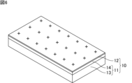
- FIG. 2 is a cross-sectional view that illustrates an example of the measurement substrate of the present invention.
- FIG. 3 is a plan view diagrammatically illustrating another example of the measuring substrate of the present invention.
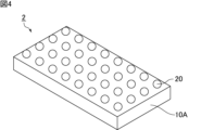
- FIG. 4 is a perspective view showing a schematic diagram of still another example of the measuring substrate of the present invention.
- FIG. 5 is a process diagram that illustrates an example of a method for producing a measurement substrate according to the present invention.
- FIG. 6 is a perspective view that illustrates an example of the insulating member prepared in the insulating member preparing step S11.
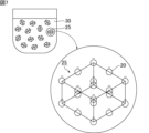
- FIG. 7 is a schematic diagram showing an example of the colloidal crystal dispersion liquid prepared in the colloidal crystal dispersion liquid preparation step S12.
- 8A and 8B are perspective views each showing a schematic example of the surface forming step S13.
- FIG. 9 is a perspective view that illustrates an example of a measuring substrate obtained by the measuring substrate
- the measurement substrate and the method for manufacturing the measurement substrate of the present invention will be described below.
- the present invention is not limited to the following embodiments, and can be appropriately modified and applied within the scope of the present invention.
- the present invention also includes a combination of two or more of the individual preferable configurations of the present invention described in the following embodiments.
- the measurement substrate of the present invention is used, for example, as an optical measurement substrate such as a surface plasmon resonance (SPR) measurement substrate.
- an optical measurement substrate such as a surface plasmon resonance (SPR) measurement substrate.
- SPR surface plasmon resonance
- FIG. 1 is a perspective view showing a schematic example of a measurement substrate of the present invention.
- FIG. 2 is a cross-sectional view showing a schematic example of a measurement substrate of the present invention.
- the measurement substrate 1 shown in Figures 1 and 2 includes an insulating member 10 and metal particles 20.
- the insulating member 10 is a conductive substrate 11 with an insulating film 12 provided on its surface.
- a MIM (Metal-Insulator-Metal) structure can be formed on the measurement substrate 1.
- the conductive substrate 11 is, for example, an insulating substrate 13 having a metal film 14 provided on its surface.
- the conductive substrate 11 may be a metal substrate, etc.
- Examples of insulating substrates 13 include glass substrates and ceramic substrates.
- the metal film 14 can be formed by methods such as vapor deposition, sputtering, and chemical plating.
- the type of metal film 14 is preferably a noble metal such as gold or silver that can exhibit strong plasmon resonance.
- the thickness of the metal film 14 is, for example, 1 nm or more and 100 nm or less. If the thickness of the metal film 14 is 100 nm or less, when the measurement substrate 1 is an SPR measurement substrate, the strength of the electric field due to the excitation of localized surface plasmons becomes stronger, and the sensitivity in the MIM-type SPR measurement becomes higher. In addition, if the thickness of the metal film 14 is 1 nm or more, pinholes are less likely to occur in the metal film 14.
- the insulating film 12 preferably has a positive or negative charge.
- the surface of the insulating member 10 preferably has a positive or negative charge.
- the insulating film 12 having a positive charge can be, for example, at least one type of insulating film selected from a silica film modified with a silane coupling agent having an aminopropyl group, and a film formed by adsorption of polyethyleneimine and poly(2-vinylpyridine).
- An example of the negatively charged insulating film 12 is a film formed by adsorption of a negatively charged polymer.
- a negatively charged polymer such as polyacrylic acid and polystyrene sulfonic acid, and introduction of negative charges such as silanol groups can be used.
- the thickness of the insulating film 12 is not particularly limited, and may be smaller than the thickness of the metal film 14, may be the same as the thickness of the metal film 14, or may be larger than the thickness of the metal film 14.
- the metal particles 20 are arranged in a single layer on the insulating member 10. In other words, the metal particles 20 are arranged two-dimensionally on the insulating member 10. It is preferable that the metal particles 20 are arranged in a single layer in all regions of the insulating member 10, but it is sufficient that the metal particles 20 are arranged in a single layer in at least some regions.
- the measurement substrate 1 is observed using a microscope such as an optical microscope or an electron microscope, if the metal particles 20 are observed only when the height of the sample stage is set to a certain height, it can be confirmed that the metal particles 20 are arranged in a single layer on the insulating member 10.
- the metal particle 20 has a core-shell structure including a core portion 21 and a shell portion 22 made of metal that covers the core portion 21.
- the specific gravity can be changed between the core portion 21 and the shell portion 22. Therefore, by making the specific gravity of the core portion 21 smaller than that of the shell portion 22, it is possible to suppress an increase in weight even if the particle diameter of the metal particles 20 is large, compared to when the metal particles 20 are solid particles made of metal. Therefore, it is possible to arrange metal particles 20 with large particle diameters in a single layer on the insulating member 10 using the method described below.
- the shell portion 22 only needs to cover at least a portion of the surface of the core portion 21. Therefore, the shell portion 22 may cover only a portion of the surface of the core portion 21, or may cover the entire surface of the core portion 21. There may be a mixture of metal particles 20 in which the shell portion 22 covers only a portion of the surface of the core portion 21, and metal particles 20 in which the shell portion 22 covers the entire surface of the core portion 21.
- the specific gravity of the core portion 21 is smaller than that of the shell portion 22.
- the particle diameter of the metal particles 20 can be increased, so that not only the near-infrared wavelength range (around 650 to 1000 nm), which is called the "biological window" and through which light easily passes through living organisms, but also higher wavelength ranges can be utilized, which is expected to improve the detection sensitivity as a biosensor.
- the peak wavelength of the surface plasmon resonance can be shifted to the longer wavelength side even if the particle diameter is the same, compared to when the metal particle 20 is a solid particle made of metal. This is presumably because the amplitude of the plasmon becomes larger due to the presence of an electrical insulator inside the metal particle 20.
- the core portion 21 is made of, for example, silicon oxide, titanium oxide, or polystyrene. From the viewpoint of making the particle diameter of the metal particles 20 uniform, silicon oxide such as SiO2 or titanium oxide such as TiO2 is preferable.
- the core portion 21 may be made of an inorganic material or an organic material.
- the core portion 21 may be made of an electrical insulator.
- the shell portion 22 is made of, for example, gold or silver. Gold is preferred from the viewpoint of suppressing oxidation and sulfurization of the metal particles 20.
- the core portion 21 is made of silicon oxide such as SiO2 and the shell portion 22 is made of gold.
- the shell portion 22 preferably has a charge of the opposite sign to the surface charge of the insulating member 10.
- the surface of the metal particle 20 preferably has a charge of the opposite sign to the surface charge of the insulating member 10.
- the metal particles 20 are arranged on the insulating member 10 at intervals due to the electrostatic repulsive force acting between the metal particles 20.
- the negatively charged metal particles 20 are adsorbed to the surface of the insulating member 10 by electrostatic attraction.
- a two-dimensional colloidal crystal in which metal particles 20 are regularly arranged is preferably formed on an insulating member 10.
- the metal particles 20 are regularly arranged two-dimensionally on the insulating member 10 with spaces between them.
- FIG. 3 is a plan view showing a schematic diagram of another example of a measurement substrate according to the present invention.
- a region (domain) in which metal particles 20 are regularly arranged in a two-dimensional manner may change orientation and become aggregated into a polycrystalline state.
- the distance between the metal particles 20 is not particularly limited, but if the distance between the metal particles 20 is too small, for example, it will be difficult for antibodies to enter, and the detection sensitivity will decrease. On the other hand, if the distance between the metal particles 20 is too large, there will be fewer metal particles 20 per unit area, and performance will decrease. For this reason, the distance between the metal particles 20 needs to be set appropriately. By setting the distance between the metal particles 20 appropriately, for example, when the measurement substrate 1 is an SPR measurement substrate, surface plasmon resonance can be actively generated.
- the distance between metal particles 20 is measured as the average interparticle distance for 100 to 200 metal particles 20 in a plan view such as that shown in Figure 3.
- the average particle size of the metal particles 20 is preferably 100 nm or more and 500 nm or less.
- the metal particles 20 have a core-shell structure, even if the average particle diameter of the metal particles 20 is 100 nm or more, the metal particles 20 can be arranged in a single layer on the insulating member 10.
- the average particle diameter of the metal particles 20 may be 150 nm or more, or 200 nm or more.
- the average particle size of the metal particles 20 is 500 nm or less, the settling speed in the liquid medium will be slow, making it easier to produce three-dimensional crystals in the manufacturing method described below.
- the average particle size of the metal particles 20 may be 450 nm or less, or may be 400 nm or less.
- the average particle size of the metal particles 20 is measured as the average particle size (diameter) of 100 or more and 200 or less metal particles 20 in a plan view such as that shown in Figure 3.
- FIG. 4 is a perspective view showing a schematic diagram of yet another example of a measurement substrate according to the present invention.
- the measurement substrate 2 shown in FIG. 4 includes an insulating member 10A and metal particles 20.
- the insulating member 10A is an insulating substrate.
- examples of the insulating member 10A include a glass substrate and a ceramic substrate.
- the measurement substrate 2 shown in FIG. 4 has a common configuration with the measurement substrate 1 shown in FIG. 1, except that it has an insulating member 10A instead of the insulating member 10. As with the insulating member 10, it is preferable that the surface of the insulating member 10A has a positive or negative charge.
- the measurement substrate of the present invention is preferably manufactured by the following method.
- FIG. 5 is a process diagram that shows a schematic example of a method for manufacturing a measurement substrate according to the present invention.
- the manufacturing method of the measurement substrate of the present invention includes an insulating member preparation process S11, a colloidal crystal dispersion preparation process S12, and a surface formation process S13.
- FIG. 6 is a schematic perspective view of an example of an insulating member prepared in the insulating member preparation step S11.
- an insulating member 10 having a positive or negative charge on its surface is prepared.
- the surface of the insulating member 10 has a positive charge.
- an insulating member 10 is prepared, which is a conductive substrate 11 having an insulating film 12 provided on its surface.
- the conductive substrate 11 is, for example, an insulating substrate 13 having a metal film 14 provided on its surface.
- the conductive substrate 11 may be a metal substrate, etc.
- an insulating substrate an insulating member 10A
- the surface of the insulating member 10A has a positive or negative charge.
- FIG. 7 is a schematic diagram showing an example of a colloidal crystal dispersion liquid prepared in the colloidal crystal dispersion liquid preparation step S12.
- a charged colloidal crystal dispersion liquid 30 is prepared in which metal colloidal crystals 25 made of metal particles 20 with a core-shell structure having a charge of the opposite sign to the surface charge of the insulating member 10 are dispersed in a dispersion medium.
- the surfaces of the metal particles 20 have a negative charge.
- the metal particle 20 has a core-shell structure including a core portion 21 and a shell portion 22 made of a metal that covers the core portion 21.
- a compound e.g., sodium 3-mercapto-1-propanesulfonate (MPS)
- a functional group e.g., mercapto group, etc.
- a functional group that forms a negative charge e.g., sulfonic acid group or carboxylic acid group, etc.
- FIGS. 8A and 8B are perspective views that show a schematic example of the surface formation process S13.
- the insulating member 10 is contacted with a charged colloidal crystal dispersion liquid 30 to form a single layer structure of metal colloidal crystals 25 on the insulating member 10.
- a negatively (or positively) charged colloidal crystal dispersion 30 is brought into contact with an insulating member 10 having a positive (or negative) charge, and only one layer of the colloidal crystal lattice is adsorbed to the insulating member 10 by electrostatic attraction, and then the excess charged colloidal crystal dispersion 30 is washed away by washing with a solvent such as water.
- FIG. 9 is a schematic perspective view of an example of a measurement substrate obtained by the measurement substrate manufacturing method of the present invention.
- a measurement substrate 1 is obtained in which a two-dimensional colloidal crystal of metal particles 20 is formed on an insulating member 10.
- the method for manufacturing a measurement substrate of the present invention forms a single layer structure of metal colloidal crystals, making it possible to control the arrangement of metal particles without using complex pattern formation techniques. This makes it easy to manufacture the measurement substrate, and allows the construction of a sensor with high detection sensitivity.
- the metal particles have a core-shell structure including a core portion and a shell portion made of a metal that covers the core portion.
- ⁇ 3> The measurement substrate according to ⁇ 1> or ⁇ 2>, wherein the measurement substrate is an optical measurement substrate.
- ⁇ 4> The measurement substrate according to ⁇ 3>, wherein the measurement substrate is a substrate for surface plasmon resonance measurement.
- ⁇ 5> The measurement substrate according to any one of ⁇ 1> to ⁇ 4>, wherein the average particle diameter of the metal particles is 100 nm or more and 500 nm or less.
- ⁇ 6> The measurement substrate according to any one of ⁇ 1> to ⁇ 5>, wherein the specific gravity of the core portion is smaller than the specific gravity of the shell portion.
- ⁇ 7> The measurement substrate according to ⁇ 6>, wherein the core portion is made of silicon oxide, titanium oxide or polystyrene.
- ⁇ 9> The measuring substrate according to any one of ⁇ 1> to ⁇ 8>, wherein the insulating member is an insulating substrate.
- insulating member is a conductive substrate having an insulating film provided on a surface thereof.
- ⁇ 11> The measurement substrate according to any one of ⁇ 1> to ⁇ 10>, wherein a two-dimensional colloidal crystal in which the metal particles are regularly arranged is formed on the insulating member.
- ⁇ 14> The method for producing a measurement substrate according to ⁇ 13>, wherein the measurement substrate is a substrate for surface plasmon resonance measurement.
- ⁇ 15> The method for manufacturing a measurement substrate according to any one of ⁇ 12> to ⁇ 14>, wherein an average particle diameter of the metal particles is 100 nm or more and 500 nm or less.
- ⁇ 16> The method for manufacturing a measurement substrate according to any one of ⁇ 12> to ⁇ 15>, wherein the specific gravity of the core portion is smaller than the specific gravity of the shell portion.
- ⁇ 17> The method for producing a measurement substrate according to ⁇ 16>, wherein the core portion is made of silicon oxide, titanium oxide or polystyrene.
- ⁇ 18> The method for manufacturing a measurement substrate according to ⁇ 16> or ⁇ 17>, wherein the shell portion is made of gold or silver.
- ⁇ 19> The method for manufacturing a measurement substrate according to any one of ⁇ 12> to ⁇ 18>, wherein the insulating member is an insulating substrate.
- ⁇ 20> The method for manufacturing a measurement substrate according to any one of ⁇ 12> to ⁇ 18>, wherein the insulating member is a conductive substrate having an insulating film provided on a surface thereof.
Landscapes
- Engineering & Computer Science (AREA)
- Chemical & Material Sciences (AREA)
- Mechanical Engineering (AREA)
- Manufacturing & Machinery (AREA)
- Analytical Chemistry (AREA)
- Composite Materials (AREA)
- General Health & Medical Sciences (AREA)
- General Physics & Mathematics (AREA)
- Immunology (AREA)
- Pathology (AREA)
- Physics & Mathematics (AREA)
- Biochemistry (AREA)
- Life Sciences & Earth Sciences (AREA)
- Materials Engineering (AREA)
- Health & Medical Sciences (AREA)
- Inorganic Chemistry (AREA)
- Nanotechnology (AREA)
- Investigating Or Analysing Materials By Optical Means (AREA)
Abstract
測定用基板1は、絶縁部材10と、絶縁部材10上に配列された金属粒子20と、を備える。絶縁部材10上に配列された金属粒子20が、少なくとも一部の領域において、単層に配列されている。金属粒子20は、コア部21と、コア部21を覆う金属からなるシェル部22とを含むコアシェル構造を有する。
Description
本発明は、測定用基板及び測定用基板の製造方法に関する。
近年、抗原抗体反応を利用した医療用のセンサー等、表面吸着を利用した様々なセンサーが開発されている。これらのセンサーには、表面吸着量を高感度で他の信号に変換するトランスデューサーとしての材料が必要となる。このようなセンサー用材料の一例として、金、銀、白金等の金属に光を照射したとき発現する、金属内の自由電子の集団的振動、すなわち、表面プラズモン共鳴(Surface Plasmon Resonance:SPR)を利用した分光分析が注目されている。この技術の原理は次のとおりである。
一般に、光は電子波(plasmon)とはカップリングしないが、金属表面においては表面固有の境界条件により光とカップリングを起こす電子波のモードが生じる。これを表面プラズモン(surface plasmon)と呼ぶ。表面プラズモンを励起する方法としては、金属表面に回折格子を形成して光とプラズモンを結合させる方法や、エバネッセント波を利用する方法がある。表面プラズモン共鳴を利用したセンサーとしては、例えば、全反射型プリズムと、当該プリズムの表面に形成された標的物質に接触する金属膜とからなるセンサーが挙げられる。このような構成により、抗原抗体反応における抗原の微量な吸着量によって表面の屈折率が変化し、これによって表面プラズモン共鳴の波長が変化するため、共鳴波長の変化から抗原の微量な吸着量のセンシングを行うことができる。
特許文献1には、表面が正又は負の電荷を有する絶縁部材を用意する絶縁部材準備工程と、上記絶縁部材の表面電荷と反対符号の電荷を有する金属コロイド粒子からなるコロイド結晶が分散媒に分散した荷電コロイド結晶分散液を調製するコロイド結晶分散液調製工程と、上記絶縁部材に上記荷電コロイド結晶分散液を接触させて、上記絶縁部材上に金属コロイド結晶の単層構造を形成させる表面形成工程と、を備えることを特徴とするSPR測定用基板の製造方法が開示されている。
特許文献1に記載の製造方法では、絶縁部材に荷電コロイド結晶分散液を接触させることにより、静電引力によって荷電コロイド結晶の一層分を絶縁部材上に吸着させる。こうして、絶縁部材上に2次元の荷電金属コロイド結晶が所定の格子間隔で並んだSPR測定用基板を製造することができる。
したがって、特許文献1に記載の製造方法によれば、金属粒子の配置を制御するためのリソグラフィー等の複雑なパターン形成技術を必要とせず、製造が容易であり、また、絶縁部材上に2次元の荷電金属コロイド結晶が所定の格子間隔で並ぶため、検出感度の高い局在型の表面プラズモンセンサーを構築することのできるSPR測定用基板を製造することができる、とされている。
バイオセンサーとして、「生体の窓」と呼ばれる、光が生体を透過しやすい近赤外の波長域(650~1000nm付近)を有効利用する場合には、例えば、粒子径の大きい金属粒子を用いて、表面プラズモン共鳴のピーク波長を長波長側にシフトさせることが必要になる。
しかしながら、特許文献1に記載の製造方法においては、金属粒子として用いられている金粒子の粒子径が通常150~200nmであり、これよりも粒子径を大きくすると、重量が増加する影響によってコロイド結晶の分散液を調製することが困難になる。そのため、2次元のコロイド結晶化層を絶縁部材上に形成することが困難になる。
なお、上記の問題は、SPR測定用基板に限らず、SPR測定用基板と同様の構成を有する測定用基板に共通する問題である。
本発明は、上記の問題を解決するためになされたものであり、金属粒子の粒子径を大きくしても、当該金属粒子を絶縁部材上に単層で配列させることが可能な測定用基板を提供することを目的とする。さらに、本発明は、金属粒子の粒子径を大きくしても、当該金属粒子からなる金属コロイド結晶の単層構造を絶縁部材上に形成することが可能な測定用基板の製造方法を提供することを目的とする。
本発明の測定用基板は、絶縁部材と、上記絶縁部材上に配列された金属粒子と、を備える。上記絶縁部材上に配列された上記金属粒子が、少なくとも一部の領域において、単層に配列されている。上記金属粒子は、コア部と、上記コア部を覆う金属からなるシェル部とを含むコアシェル構造を有する。
本発明の測定用基板の製造方法は、表面が正又は負の電荷を有する絶縁部材を準備する絶縁部材準備工程と、上記絶縁部材の表面電荷と反対符号の電荷を有するコアシェル構造の金属粒子からなる金属コロイド結晶が分散媒に分散した荷電コロイド結晶分散液を調製するコロイド結晶分散液調製工程と、上記絶縁部材に上記荷電コロイド結晶分散液を接触させて、上記絶縁部材上に上記金属コロイド結晶の単層構造を形成する表面形成工程と、を備える。
本発明によれば、金属粒子の粒子径を大きくしても、当該金属粒子を絶縁部材上に単層で配列させることが可能な測定用基板を提供することができる。さらに、本発明によれば、金属粒子の粒子径を大きくしても、当該金属粒子からなる金属コロイド結晶の単層構造を絶縁部材上に形成することが可能な測定用基板の製造方法を提供することができる。
以下、本発明の測定用基板及び測定用基板の製造方法について説明する。
しかしながら、本発明は、以下の実施形態に限定されるものではなく、本発明の要旨を変更しない範囲において適宜変更して適用することができる。以下の実施形態において記載する本発明の個々の望ましい構成を2つ以上組み合わせたものもまた本発明である。
しかしながら、本発明は、以下の実施形態に限定されるものではなく、本発明の要旨を変更しない範囲において適宜変更して適用することができる。以下の実施形態において記載する本発明の個々の望ましい構成を2つ以上組み合わせたものもまた本発明である。
本発明の測定用基板は、例えば、表面プラズモン共鳴(SPR)測定用基板等の光学測定用基板として用いられる。
以下に示す図面は模式図であり、その寸法、縦横比の縮尺等は実際の製品と異なる場合がある。図中、同一又は相当部分には同一符号を用いることとする。また、各図において、同一要素には同一符号を付して重複する説明を省略する。
図1は、本発明の測定用基板の一例を模式的に示す斜視図である。図2は、本発明の測定用基板の一例を模式的に示す断面図である。
図1及び図2に示す測定用基板1は、絶縁部材10と、金属粒子20と、を備える。
図1及び図2に示す例では、絶縁部材10は、表面に絶縁膜12が設けられた導電性の基板11である。この場合、測定用基板1にMIM(Metal-Insulator-Metal)構造を形成することができる。
導電性の基板11は、例えば、表面に金属膜14が設けられた絶縁性の基板13である。あるいは、導電性の基板11は、金属基板等であってもよい。
絶縁性の基板13としては、例えば、ガラス基板、セラミック基板等が挙げられる。
金属膜14は、例えば、蒸着、スパッタリング、化学めっき等の方法により形成することができる。
測定用基板1がSPR測定用基板である場合、金属膜14の種類としては、強いプラズモン共鳴を示し得る金又は銀等の貴金属が好適である。
金属膜14の厚さは、例えば、1nm以上、100nm以下である。金属膜14の厚さが100nm以下であると、測定用基板1がSPR測定用基板である場合に、局在型の表面プラズモンの励起による電場の強さが強くなるため、MIM型SPR測定における感度が高くなる。また、金属膜14の厚さが1nm以上であると、金属膜14にピンホールが生じにくくなる。
絶縁膜12は、正又は負の電荷を有することが好ましい。すなわち、絶縁部材10の表面は、正又は負の電荷を有することが好ましい。
正電荷を有する絶縁膜12としては、例えば、アミノプロピル基を有するシランカップリング剤で修飾したシリカ膜や、ポリエチレンイミン及びポリ(2-ビニルピリジン)の吸着により形成される膜より選ばれる少なくとも1種の絶縁膜が挙げられる。
負電荷を有する絶縁膜12としては、例えば、負電荷を有する高分子の吸着により形成される膜が挙げられる。絶縁皮膜に負電荷を与えるためには、例えば、ポリアクリル酸、ポリスチレンスルホン酸等のアニオン性高分子電解質の吸着、シラノール基等の負荷電の導入等の方法が利用できる。
絶縁膜12の厚さは特に限定されず、金属膜14の厚さより小さくてもよく、金属膜14の厚さと同じでもよく、金属膜14の厚さより大きくてもよい。
金属粒子20は、絶縁部材10上に単層で配列されている。言い換えると、金属粒子20は、絶縁部材10上に2次元的に配列されている。なお、金属粒子20は絶縁部材10の全ての領域において単層で配列されていることが好ましいが、少なくとも一部の領域において単層で配列されていればよい。
例えば、光学顕微鏡、電子顕微鏡等の顕微鏡を用いて測定用基板1を観察した際、試料台の高さを一定の高さに設定したときのみ金属粒子20が観察される場合、金属粒子20が絶縁部材10上に単層で配列されていると確認することができる。
図2に示すように、金属粒子20は、コア部21と、コア部21を覆う金属からなるシェル部22とを含むコアシェル構造を有する。
金属粒子20がコアシェル構造を有する場合、コア部21とシェル部22とで比重を変えることができる。そのため、コア部21の比重をシェル部22の比重より小さくすることにより、金属粒子20が金属からなる中実粒子である場合に比べて、金属粒子20の粒子径を大きくしても重量の増加を抑制することができる。したがって、後述する方法を用いて、粒子径の大きな金属粒子20を絶縁部材10上に単層で配列させることが可能になる。
シェル部22は、コア部21の表面の少なくとも一部のみを覆っていればよい。そのため、シェル部22は、コア部21の表面の一部のみを覆っていてもよく、コア部21の表面の全体を覆っていてもよい。シェル部22がコア部21の表面の一部のみを覆う金属粒子20と、シェル部22がコア部21の表面の全体を覆う金属粒子20とが混在してもよい。
上記のとおり、コア部21の比重は、シェル部22の比重より小さいことが好ましい。コア部21及びシェル部22の比重を調整することにより、金属粒子20の粒子径を大きくできるため、「生体の窓」と呼ばれる、光が生体を透過しやすい近赤外の波長域(650~1000nm付近)だけでなく、更なる高波長域も利用可能になり、バイオセンサーとしての検出感度の向上が期待できる。
また、金属粒子20のコア部21が電気絶縁体から構成される場合には、金属粒子20が金属からなる中実粒子である場合に比べて、粒子径が同じであっても表面プラズモン共鳴のピーク波長を長波長側にシフトさせることができる。その理由としては、金属粒子20の内部に電気絶縁体が存在することにより、プラズモンの振幅が大きくなるためではないかと推定される。
コア部21は、例えば、酸化ケイ素、酸化チタン又はポリスチレンからなる。金属粒子20の粒子径を揃える観点からは、SiO2等の酸化ケイ素又はTiO2等の酸化チタンが好ましい。コア部21は、無機物から構成されてもよく、有機物から構成されてもよい。コア部21は、電気絶縁体から構成されてもよい。
シェル部22は、例えば、金又は銀からなる。金属粒子20の酸化及び硫化を抑える観点からは、金が好ましい。
中でも、コア部21がSiO2等の酸化ケイ素からなり、シェル部22が金からなることが好ましい。
シェル部22は、絶縁部材10の表面電荷と反対符号の電荷を有することが好ましい。すなわち、金属粒子20の表面は、絶縁部材10の表面電荷と反対符号の電荷を有することが好ましい。
図2に示すように、例えば、絶縁部材10の表面(図2に示す例では絶縁膜12)が正電荷を有し、金属粒子20の表面が負電荷を有する場合、金属粒子20同士は、金属粒子20の間に働く静電的な反発力によって、間隔を空けて絶縁部材10上に配列される。一方、絶縁部材10の表面が正電荷を有するため、負電荷を有する金属粒子20は静電引力によって絶縁部材10の表面に吸着する。
図1に示す測定用基板1のように、絶縁部材10上には、金属粒子20が規則的に配列された2次元コロイド結晶が形成されていることが好ましい。この場合、金属粒子20同士は、間隔を空けて絶縁部材10上に2次元的に規則的に並んで配置されていることが好ましい。
図3は、本発明の測定用基板の別の一例を模式的に示す平面図である。
図3に示す測定用基板1Aのように、金属粒子20が2次元的に規則的に配列されている領域(ドメイン)が、向きを変えて凝集した多結晶状態になっていてもよい。
なお、図1又は図3には示されていないが、絶縁部材10上に金属粒子20の2次元コロイド結晶が形成されている場合、金属粒子20が規則的に配列されている領域のみが存在してもよく、金属粒子20が規則的に配列されている領域に加えて、金属粒子20が不規則に配列されている領域が存在してもよい。
金属粒子20同士の間隔は特に限定されないが、金属粒子20同士の間隔が小さ過ぎると、例えば抗体が入りにくくなり、検出感度が落ちる。一方、金属粒子20同士の間隔が大き過ぎると、単位面積当たりの金属粒子20が少なくなり、性能が落ちる。そのため、金属粒子20同士の間隔は適切に設定する必要がある。金属粒子20同士の間隔を適切に設定することで、例えば測定用基板1がSPR測定用基板である場合、表面プラズモン共鳴を活発に発生させることができる。
金属粒子20同士の間隔は、図3に示すような平面図において、100個以上、200個以下の金属粒子20を対象とする粒子間距離の平均値として測定される。
金属粒子20の平均粒子径は、100nm以上、500nm以下であることが好ましい。
上記のとおり、金属粒子20がコアシェル構造を有するため、金属粒子20の平均粒子径が100nm以上であっても、金属粒子20を絶縁部材10上に単層で配列させることができる。金属粒子20の平均粒子径は、150nm以上であってもよく、200nm以上であってもよい。
一方、金属粒子20の平均粒子径が500nm以下であると、液体媒体中での沈降速度が遅くなるため、後述する製造方法において3次元結晶が生成されやすくなる。金属粒子20の平均粒子径は、450nm以下であってもよく、400nm以下であってもよい。
金属粒子20の平均粒子径は、図3に示すような平面図において、100個以上、200個以下の金属粒子20を対象とする粒子径(直径)の平均値として測定される。
図4は、本発明の測定用基板のさらに別の一例を模式的に示す斜視図である。
図4に示す測定用基板2は、絶縁部材10Aと、金属粒子20と、を備える。
図4に示す例では、絶縁部材10Aは、絶縁性の基板である。この場合、絶縁部材10Aとしては、例えば、ガラス基板、セラミック基板等が挙げられる。
図4に示す測定用基板2は、絶縁部材10に代えて絶縁部材10Aを備えることを除いて、図1に示す測定用基板1と共通の構成を有する。絶縁部材10と同様、絶縁部材10Aの表面は、正又は負の電荷を有することが好ましい。
本発明の測定用基板は、好ましくは、以下の方法により製造される。
図5は、本発明の測定用基板の製造方法の一例を模式的に示す工程図である。
本発明の測定用基板の製造方法は、絶縁部材準備工程S11と、コロイド結晶分散液調製工程S12と、表面形成工程S13と、を備える。
図6は、絶縁部材準備工程S11で準備される絶縁部材の一例を模式的に示す斜視図である。
絶縁部材準備工程S11では、表面が正又は負の電荷を有する絶縁部材10を準備する。図6に示す例では、絶縁部材10の表面は正電荷を有する。
例えば、図1に示す測定用基板1を製造する場合、表面に絶縁膜12が設けられた導電性の基板11である絶縁部材10が準備される。導電性の基板11は、例えば、表面に金属膜14が設けられた絶縁性の基板13である。あるいは、導電性の基板11は、金属基板等であってもよい。
一方、図4に示す測定用基板2を製造する場合、絶縁部材準備工程S11では、絶縁性の基板である絶縁部材10Aが準備される。絶縁部材10Aの表面は、正又は負の電荷を有する。
図7は、コロイド結晶分散液調製工程S12で調製されるコロイド結晶分散液の一例を示す模式図である。
コロイド結晶分散液調製工程S12では、絶縁部材10の表面電荷と反対符号の電荷を有するコアシェル構造の金属粒子20からなる金属コロイド結晶25が分散媒に分散した荷電コロイド結晶分散液30を調製する。図7に示す例では、金属粒子20の表面は負電荷を有する。
図7には示されていないが、図1において説明したとおり、金属粒子20は、コア部21と、コア部21を覆う金属からなるシェル部22とを含むコアシェル構造を有する。
例えば、金属粒子20のコロイド分散液に、シェル部22を構成する金属と結合する官能基(例えばメルカプト基等)及び負電荷を形成する官能基(例えばスルホン酸基又はカルボン酸基等)を有する化合物(例えば、3-メルカプト-1-プロパンスルホン酸ナトリウム(MPS)等)を添加する。そして、イオン交換樹脂を添加する等して不純物イオンを除去すると、粒子間の静電斥力が十分強くなり、分散液中で荷電コロイド結晶構造が形成され、金属粒子20が所定の間隔で配列した荷電コロイド結晶分散液30が調製される。
図8A及び図8Bは、表面形成工程S13の一例を模式的に示す斜視図である。
表面形成工程S13では、絶縁部材10に荷電コロイド結晶分散液30を接触させて、絶縁部材10上に金属コロイド結晶25の単層構造を形成する。
具体的には、正(又は負)の電荷を有する絶縁部材10上に負(又は正)の電荷を有する荷電コロイド結晶分散液30を接触させ、静電引力によって、コロイド結晶格子の一層だけを絶縁部材10に吸着させた後、水等の溶媒で洗浄して余分な荷電コロイド結晶分散液30を洗い流す。
図9は、本発明の測定用基板の製造方法により得られる測定用基板の一例を模式的に示す斜視図である。
以上の工程により、例えば、金属粒子20の2次元コロイド結晶が絶縁部材10上に形成された測定用基板1が得られる。
本発明の測定用基板の製造方法によれば、金属コロイド結晶の単層構造が形成されることにより、複雑なパターン形成技術を用いなくても、金属粒子の配置を制御することができる。そのため、測定用基板の製造が容易であり、かつ、検出感度の高いセンサーを構築することができる。
本明細書には、以下の内容が開示されている。
<1>
絶縁部材と、
上記絶縁部材上に配列された金属粒子と、を備え、
上記絶縁部材上に配列された上記金属粒子が、少なくとも一部の領域において、単層に配列され、
上記金属粒子は、コア部と、上記コア部を覆う金属からなるシェル部とを含むコアシェル構造を有する、測定用基板。
絶縁部材と、
上記絶縁部材上に配列された金属粒子と、を備え、
上記絶縁部材上に配列された上記金属粒子が、少なくとも一部の領域において、単層に配列され、
上記金属粒子は、コア部と、上記コア部を覆う金属からなるシェル部とを含むコアシェル構造を有する、測定用基板。
<2>
上記絶縁部材上に配列された上記金属粒子が、全ての領域において、単層に配列されている、<1>に記載の測定用基板。
上記絶縁部材上に配列された上記金属粒子が、全ての領域において、単層に配列されている、<1>に記載の測定用基板。
<3>
上記測定用基板が光学測定用基板である、<1>又は<2>に記載の測定用基板。
上記測定用基板が光学測定用基板である、<1>又は<2>に記載の測定用基板。
<4>
上記測定用基板が表面プラズモン共鳴測定用基板である、<3>に記載の測定用基板。
上記測定用基板が表面プラズモン共鳴測定用基板である、<3>に記載の測定用基板。
<5>
上記金属粒子の平均粒子径は、100nm以上、500nm以下である、<1>~<4>のいずれか1つに記載の測定用基板。
上記金属粒子の平均粒子径は、100nm以上、500nm以下である、<1>~<4>のいずれか1つに記載の測定用基板。
<6>
上記コア部の比重は、上記シェル部の比重より小さい、<1>~<5>のいずれか1つに記載の測定用基板。
上記コア部の比重は、上記シェル部の比重より小さい、<1>~<5>のいずれか1つに記載の測定用基板。
<7>
上記コア部は、酸化ケイ素、酸化チタン又はポリスチレンからなる、<6>に記載の測定用基板。
上記コア部は、酸化ケイ素、酸化チタン又はポリスチレンからなる、<6>に記載の測定用基板。
<8>
上記シェル部は、金又は銀からなる、<6>又は<7>に記載の測定用基板。
上記シェル部は、金又は銀からなる、<6>又は<7>に記載の測定用基板。
<9>
上記絶縁部材は、絶縁性の基板である、<1>~<8>のいずれか1つに記載の測定用基板。
上記絶縁部材は、絶縁性の基板である、<1>~<8>のいずれか1つに記載の測定用基板。
<10>
上記絶縁部材は、表面に絶縁膜が設けられた導電性の基板である、<1>~<8>のいずれか1つに記載の測定用基板。
上記絶縁部材は、表面に絶縁膜が設けられた導電性の基板である、<1>~<8>のいずれか1つに記載の測定用基板。
<11>
上記絶縁部材上には、上記金属粒子が規則的に配列された2次元コロイド結晶が形成されている、<1>~<10>のいずれか1つに記載の測定用基板。
上記絶縁部材上には、上記金属粒子が規則的に配列された2次元コロイド結晶が形成されている、<1>~<10>のいずれか1つに記載の測定用基板。
<12>
表面が正又は負の電荷を有する絶縁部材を準備する絶縁部材準備工程と、
上記絶縁部材の表面電荷と反対符号の電荷を有するコアシェル構造の金属粒子からなる金属コロイド結晶が分散媒に分散した荷電コロイド結晶分散液を調製するコロイド結晶分散液調製工程と、
上記絶縁部材に上記荷電コロイド結晶分散液を接触させて、上記絶縁部材上に上記金属コロイド結晶の単層構造を形成する表面形成工程と、を備える、測定用基板の製造方法。
表面が正又は負の電荷を有する絶縁部材を準備する絶縁部材準備工程と、
上記絶縁部材の表面電荷と反対符号の電荷を有するコアシェル構造の金属粒子からなる金属コロイド結晶が分散媒に分散した荷電コロイド結晶分散液を調製するコロイド結晶分散液調製工程と、
上記絶縁部材に上記荷電コロイド結晶分散液を接触させて、上記絶縁部材上に上記金属コロイド結晶の単層構造を形成する表面形成工程と、を備える、測定用基板の製造方法。
<13>
上記測定用基板が光学測定用基板である、<12>に記載の測定用基板の製造方法。
上記測定用基板が光学測定用基板である、<12>に記載の測定用基板の製造方法。
<14>
上記測定用基板が表面プラズモン共鳴測定用基板である、<13>に記載の測定用基板の製造方法。
上記測定用基板が表面プラズモン共鳴測定用基板である、<13>に記載の測定用基板の製造方法。
<15>
上記金属粒子の平均粒子径は、100nm以上、500nm以下である、<12>~<14>のいずれか1つに記載の測定用基板の製造方法。
上記金属粒子の平均粒子径は、100nm以上、500nm以下である、<12>~<14>のいずれか1つに記載の測定用基板の製造方法。
<16>
上記コア部の比重は、上記シェル部の比重より小さい、<12>~<15>のいずれか1つに記載の測定用基板の製造方法。
上記コア部の比重は、上記シェル部の比重より小さい、<12>~<15>のいずれか1つに記載の測定用基板の製造方法。
<17>
上記コア部は、酸化ケイ素、酸化チタン又はポリスチレンからなる、<16>に記載の測定用基板の製造方法。
上記コア部は、酸化ケイ素、酸化チタン又はポリスチレンからなる、<16>に記載の測定用基板の製造方法。
<18>
上記シェル部は、金又は銀からなる、<16>又は<17>に記載の測定用基板の製造方法。
上記シェル部は、金又は銀からなる、<16>又は<17>に記載の測定用基板の製造方法。
<19>
上記絶縁部材は、絶縁性の基板である、<12>~<18>のいずれか1つに記載の測定用基板の製造方法。
上記絶縁部材は、絶縁性の基板である、<12>~<18>のいずれか1つに記載の測定用基板の製造方法。
<20>
上記絶縁部材は、表面に絶縁膜が設けられた導電性の基板である、<12>~<18>のいずれか1つに記載の測定用基板の製造方法。
上記絶縁部材は、表面に絶縁膜が設けられた導電性の基板である、<12>~<18>のいずれか1つに記載の測定用基板の製造方法。
1、1A、2 測定用基板
10、10A 絶縁部材
11 導電性の基板
12 絶縁膜
13 絶縁性の基板
14 金属膜
20 金属粒子
21 コア部
22 シェル部
25 金属コロイド結晶
30 荷電コロイド結晶分散液
10、10A 絶縁部材
11 導電性の基板
12 絶縁膜
13 絶縁性の基板
14 金属膜
20 金属粒子
21 コア部
22 シェル部
25 金属コロイド結晶
30 荷電コロイド結晶分散液
Claims (12)
- 絶縁部材と、
前記絶縁部材上に配列された金属粒子と、を備え、
前記絶縁部材上に配列された前記金属粒子が、少なくとも一部の領域において、単層に配列され、
前記金属粒子は、コア部と、前記コア部を覆う金属からなるシェル部とを含むコアシェル構造を有する、測定用基板。 - 前記絶縁部材上に配列された前記金属粒子が、全ての領域において、単層に配列されている、請求項1に記載の測定用基板。
- 前記測定用基板が光学測定用基板である、請求項1又は2に記載の測定用基板。
- 前記測定用基板が表面プラズモン共鳴測定用基板である、請求項3に記載の測定用基板。
- 前記金属粒子の平均粒子径は、100nm以上、500nm以下である、請求項1~4のいずれか1項に記載の測定用基板。
- 前記コア部の比重は、前記シェル部の比重より小さい、請求項1~5のいずれか1項に記載の測定用基板。
- 前記コア部は、酸化ケイ素、酸化チタン又はポリスチレンからなる、請求項6に記載の測定用基板。
- 前記シェル部は、金又は銀からなる、請求項6又は7に記載の測定用基板。
- 前記絶縁部材は、絶縁性の基板である、請求項1~8のいずれか1項に記載の測定用基板。
- 前記絶縁部材は、表面に絶縁膜が設けられた導電性の基板である、請求項1~8のいずれか1項に記載の測定用基板。
- 前記絶縁部材上には、前記金属粒子が規則的に配列された2次元コロイド結晶が形成されている、請求項1~10のいずれか1項に記載の測定用基板。
- 表面が正又は負の電荷を有する絶縁部材を準備する絶縁部材準備工程と、
前記絶縁部材の表面電荷と反対符号の電荷を有するコアシェル構造の金属粒子からなる金属コロイド結晶が分散媒に分散した荷電コロイド結晶分散液を調製するコロイド結晶分散液調製工程と、
前記絶縁部材に前記荷電コロイド結晶分散液を接触させて、前記絶縁部材上に前記金属コロイド結晶の単層構造を形成する表面形成工程と、を備える、測定用基板の製造方法。
Priority Applications (1)
| Application Number | Priority Date | Filing Date | Title |
|---|---|---|---|
| JP2025525933A JPWO2024252697A1 (ja) | 2023-06-09 | 2023-12-20 |
Applications Claiming Priority (2)
| Application Number | Priority Date | Filing Date | Title |
|---|---|---|---|
| JP2023-095591 | 2023-06-09 | ||
| JP2023095591 | 2023-06-09 |
Publications (1)
| Publication Number | Publication Date |
|---|---|
| WO2024252697A1 true WO2024252697A1 (ja) | 2024-12-12 |
Family
ID=93795864
Family Applications (1)
| Application Number | Title | Priority Date | Filing Date |
|---|---|---|---|
| PCT/JP2023/045689 Ceased WO2024252697A1 (ja) | 2023-06-09 | 2023-12-20 | 測定用基板及び測定用基板の製造方法 |
Country Status (2)
| Country | Link |
|---|---|
| JP (1) | JPWO2024252697A1 (ja) |
| WO (1) | WO2024252697A1 (ja) |
Citations (3)
| Publication number | Priority date | Publication date | Assignee | Title |
|---|---|---|---|---|
| JP2010127928A (ja) * | 2008-11-29 | 2010-06-10 | Korea Electronics Telecommun | バイオ物質感知用ナノ粒子及びこれを利用したバイオセンサ |
| JP2013522639A (ja) * | 2010-03-22 | 2013-06-13 | アイメック | 表面増強光検出のための方法およびシステム |
| JP2020034543A (ja) * | 2018-08-28 | 2020-03-05 | 公立大学法人名古屋市立大学 | Spr測定用基板及びその製造方法 |
-
2023
- 2023-12-20 WO PCT/JP2023/045689 patent/WO2024252697A1/ja not_active Ceased
- 2023-12-20 JP JP2025525933A patent/JPWO2024252697A1/ja active Pending
Patent Citations (3)
| Publication number | Priority date | Publication date | Assignee | Title |
|---|---|---|---|---|
| JP2010127928A (ja) * | 2008-11-29 | 2010-06-10 | Korea Electronics Telecommun | バイオ物質感知用ナノ粒子及びこれを利用したバイオセンサ |
| JP2013522639A (ja) * | 2010-03-22 | 2013-06-13 | アイメック | 表面増強光検出のための方法およびシステム |
| JP2020034543A (ja) * | 2018-08-28 | 2020-03-05 | 公立大学法人名古屋市立大学 | Spr測定用基板及びその製造方法 |
Non-Patent Citations (1)
| Title |
|---|
| NICOLAS RANA, LÉVÊQUE GAËTAN, MARAE-DJOUDA JOSEPH, MONTAY GUILLAME, MADI YAZID, PLAIN JÉRÔME, HERRO ZIAD, KAZAN MICHEL, ADAM PIERR: "Plasmonic mode interferences and Fano resonances in Metal-Insulator- Metal nanostructured interface", SCIENTIFIC REPORTS, NATURE PUBLISHING GROUP, US, vol. 5, no. 1, US , XP093246225, ISSN: 2045-2322, DOI: 10.1038/srep14419 * |
Also Published As
| Publication number | Publication date |
|---|---|
| JPWO2024252697A1 (ja) | 2024-12-12 |
Similar Documents
| Publication | Publication Date | Title |
|---|---|---|
| Lednický et al. | Large scale fabrication of ordered gold nanoparticle–epoxy surface nanocomposites and their application as label-free plasmonic DNA biosensors | |
| Wang et al. | Research advances on surface plasmon resonance biosensors | |
| Kaushik et al. | Two-dimensional transition metal dichalcogenides assisted biofunctionalized optical fiber SPR biosensor for efficient and rapid detection of bovine serum albumin | |
| Mariani et al. | Decoration of porous silicon with gold nanoparticles via layer-by-layer nanoassembly for interferometric and hybrid photonic/plasmonic (bio) sensing | |
| Qian et al. | Three-dimensionally ordered macroporous polymer materials: An approach for biosensor applications | |
| Chen et al. | Shape-dependent refractive index sensitivities of gold nanocrystals with the same plasmon resonance wavelength | |
| Martinsson et al. | Substrate effect on the refractive index sensitivity of silver nanoparticles | |
| Gehan et al. | Thermo-induced electromagnetic coupling in gold/polymer hybrid plasmonic structures probed by surface-enhanced Raman scattering | |
| Verre et al. | Metasurfaces and colloidal suspensions composed of 3D chiral Si nanoresonators | |
| Solanki et al. | A chitosan modified nickel oxide platform for biosensing applications | |
| He et al. | Suspension array with shape-coded silica nanotubes for multiplexed immunoassays | |
| JP7253169B2 (ja) | Spr測定用基板及びその製造方法 | |
| CN111213051B (zh) | 用于确定分析物的纳米传感器方法和装置 | |
| WO2012169971A1 (en) | Method of generating a metamaterial, and a metamaterial generated thereof | |
| Li et al. | Fabrication of an insect-like compound-eye SERS substrate with 3D Ag nano-bowls and its application in optical sensor | |
| Schalkhammer | Metal nano clusters as transducers for bioaffinity interactions | |
| Zhao et al. | TiN nanorods as effective substrate for surface-enhanced Raman scattering | |
| CN101919080B (zh) | 利用光学特性的传感器的基板制造方法及由此制造的基板 | |
| JP2005144569A (ja) | 二次元配列構造体基板および該基板から剥離した微粒子 | |
| KR102500117B1 (ko) | 플라즈몬 나노입자와 수화젤 입자로 구성된 나노입자 복합체의 패턴화 및 패턴화된 나노구조체의 제조, 이를 통한 광학적 신호 및 sers 신호의 조절 | |
| WO2014129933A1 (ru) | Биологический сенсор и способ создания биологического сенсора | |
| Zhang et al. | Metallic nanoshells with sub-10 nm thickness and their performance as surface-enhanced spectroscopy substrate | |
| US20240402165A1 (en) | Spiky metal structures | |
| Putranto et al. | Block copolymer self-assembly for biological and chemical sensing | |
| CN110618478B (zh) | 一种基于单个金属银纳米颗粒-金属银薄膜的Fano共振结构及其制备方法 |
Legal Events
| Date | Code | Title | Description |
|---|---|---|---|
| 121 | Ep: the epo has been informed by wipo that ep was designated in this application |
Ref document number: 23940791 Country of ref document: EP Kind code of ref document: A1 |
|
| ENP | Entry into the national phase |
Ref document number: 2025525933 Country of ref document: JP Kind code of ref document: A |
|
| WWE | Wipo information: entry into national phase |
Ref document number: 2025525933 Country of ref document: JP |
|
| NENP | Non-entry into the national phase |
Ref country code: DE |