WO2024252660A1 - 半導体装置 - Google Patents
半導体装置 Download PDFInfo
- Publication number
- WO2024252660A1 WO2024252660A1 PCT/JP2023/021508 JP2023021508W WO2024252660A1 WO 2024252660 A1 WO2024252660 A1 WO 2024252660A1 JP 2023021508 W JP2023021508 W JP 2023021508W WO 2024252660 A1 WO2024252660 A1 WO 2024252660A1
- Authority
- WO
- WIPO (PCT)
- Prior art keywords
- power supply
- supply line
- transistor
- power
- substrate
- Prior art date
- Legal status (The legal status is an assumption and is not a legal conclusion. Google has not performed a legal analysis and makes no representation as to the accuracy of the status listed.)
- Ceased
Links
Images








Classifications
-
- H—ELECTRICITY
- H10—SEMICONDUCTOR DEVICES; ELECTRIC SOLID-STATE DEVICES NOT OTHERWISE PROVIDED FOR
- H10W—GENERIC PACKAGES, INTERCONNECTIONS, CONNECTORS OR OTHER CONSTRUCTIONAL DETAILS OF DEVICES COVERED BY CLASS H10
- H10W20/00—Interconnections in chips, wafers or substrates
- H10W20/40—Interconnections external to wafers or substrates, e.g. back-end-of-line [BEOL] metallisations or vias connecting to gate electrodes
- H10W20/41—Interconnections external to wafers or substrates, e.g. back-end-of-line [BEOL] metallisations or vias connecting to gate electrodes characterised by their conductive parts
- H10W20/427—Power or ground buses
-
- H—ELECTRICITY
- H02—GENERATION; CONVERSION OR DISTRIBUTION OF ELECTRIC POWER
- H02M—APPARATUS FOR CONVERSION BETWEEN AC AND AC, BETWEEN AC AND DC, OR BETWEEN DC AND DC, AND FOR USE WITH MAINS OR SIMILAR POWER SUPPLY SYSTEMS; CONVERSION OF DC OR AC INPUT POWER INTO SURGE OUTPUT POWER; CONTROL OR REGULATION THEREOF
- H02M7/00—Conversion of AC power input into DC power output; Conversion of DC power input into AC power output
- H02M7/42—Conversion of DC power input into AC power output without possibility of reversal
- H02M7/44—Conversion of DC power input into AC power output without possibility of reversal by static converters
- H02M7/48—Conversion of DC power input into AC power output without possibility of reversal by static converters using discharge tubes with control electrode or semiconductor devices with control electrode
- H02M7/53—Conversion of DC power input into AC power output without possibility of reversal by static converters using discharge tubes with control electrode or semiconductor devices with control electrode using devices of a triode or transistor type requiring continuous application of a control signal
- H02M7/537—Conversion of DC power input into AC power output without possibility of reversal by static converters using discharge tubes with control electrode or semiconductor devices with control electrode using devices of a triode or transistor type requiring continuous application of a control signal using semiconductor devices only, e.g. single switched pulse inverters
-
- H—ELECTRICITY
- H10—SEMICONDUCTOR DEVICES; ELECTRIC SOLID-STATE DEVICES NOT OTHERWISE PROVIDED FOR
- H10D—INORGANIC ELECTRIC SEMICONDUCTOR DEVICES
- H10D84/00—Integrated devices formed in or on semiconductor substrates that comprise only semiconducting layers, e.g. on Si wafers or on GaAs-on-Si wafers
-
- H—ELECTRICITY
- H10—SEMICONDUCTOR DEVICES; ELECTRIC SOLID-STATE DEVICES NOT OTHERWISE PROVIDED FOR
- H10D—INORGANIC ELECTRIC SEMICONDUCTOR DEVICES
- H10D84/00—Integrated devices formed in or on semiconductor substrates that comprise only semiconducting layers, e.g. on Si wafers or on GaAs-on-Si wafers
- H10D84/01—Manufacture or treatment
- H10D84/02—Manufacture or treatment characterised by using material-based technologies
- H10D84/03—Manufacture or treatment characterised by using material-based technologies using Group IV technology, e.g. silicon technology or silicon-carbide [SiC] technology
- H10D84/038—Manufacture or treatment characterised by using material-based technologies using Group IV technology, e.g. silicon technology or silicon-carbide [SiC] technology using silicon technology, e.g. SiGe
-
- H—ELECTRICITY
- H10—SEMICONDUCTOR DEVICES; ELECTRIC SOLID-STATE DEVICES NOT OTHERWISE PROVIDED FOR
- H10W—GENERIC PACKAGES, INTERCONNECTIONS, CONNECTORS OR OTHER CONSTRUCTIONAL DETAILS OF DEVICES COVERED BY CLASS H10
- H10W20/00—Interconnections in chips, wafers or substrates
- H10W20/40—Interconnections external to wafers or substrates, e.g. back-end-of-line [BEOL] metallisations or vias connecting to gate electrodes
- H10W20/41—Interconnections external to wafers or substrates, e.g. back-end-of-line [BEOL] metallisations or vias connecting to gate electrodes characterised by their conductive parts
- H10W20/42—Vias, e.g. via plugs
-
- H—ELECTRICITY
- H10—SEMICONDUCTOR DEVICES; ELECTRIC SOLID-STATE DEVICES NOT OTHERWISE PROVIDED FOR
- H10W—GENERIC PACKAGES, INTERCONNECTIONS, CONNECTORS OR OTHER CONSTRUCTIONAL DETAILS OF DEVICES COVERED BY CLASS H10
- H10W20/00—Interconnections in chips, wafers or substrates
- H10W20/40—Interconnections external to wafers or substrates, e.g. back-end-of-line [BEOL] metallisations or vias connecting to gate electrodes
- H10W20/41—Interconnections external to wafers or substrates, e.g. back-end-of-line [BEOL] metallisations or vias connecting to gate electrodes characterised by their conductive parts
- H10W20/43—Layouts of interconnections
-
- H—ELECTRICITY
- H10—SEMICONDUCTOR DEVICES; ELECTRIC SOLID-STATE DEVICES NOT OTHERWISE PROVIDED FOR
- H10W—GENERIC PACKAGES, INTERCONNECTIONS, CONNECTORS OR OTHER CONSTRUCTIONAL DETAILS OF DEVICES COVERED BY CLASS H10
- H10W20/00—Interconnections in chips, wafers or substrates
- H10W20/40—Interconnections external to wafers or substrates, e.g. back-end-of-line [BEOL] metallisations or vias connecting to gate electrodes
- H10W20/41—Interconnections external to wafers or substrates, e.g. back-end-of-line [BEOL] metallisations or vias connecting to gate electrodes characterised by their conductive parts
- H10W20/435—Cross-sectional shapes or dispositions of interconnections
Definitions
- the present invention relates to a semiconductor device.
- AOB always on Buffer
- BS-PDN Backside Power Delivery Network
- a technology is known in which vias are directly connected from below the semiconductor substrate to the source and drain of a transistor on the surface of the semiconductor substrate.
- the present invention has been made in consideration of the above points, and aims to efficiently arrange buffers including transistors whose sources and drains are directly connected to wiring below the substrate through vias.
- a semiconductor device in one aspect of the present invention, includes a substrate, a first power supply line formed below the substrate and supplied with a first potential, a second power supply line supplied with a second potential, a third power supply line supplied with a third potential, a first transistor formed above the substrate and arranged to overlap the first power supply line in a planar view, a second transistor formed above the substrate, and a first via formed in the substrate and connecting the source of the first transistor to the first power supply line.
- the disclosed technology allows for efficient placement of buffers including transistors whose sources and drains are directly connected to wiring below the substrate through vias.
- FIG. 2 is a plan view showing an example of a layout of the semiconductor device according to the first embodiment.
- 2 is a cross-sectional view showing an example of a cross-sectional structure of the semiconductor device of FIG. 1;
- 2 is a circuit diagram showing an example of a circuit arranged in the standard cell block of FIG. 1;
- 4 is a plan view showing an example of the positional relationship between the power lines and vias arranged in the power domain PD2 of FIG. 3 and the AOB in a plan view on the rear surface side of the semiconductor substrate.
- FIG. 5 is a plan view showing an example of the layout of the AOB in FIG. 4 .
- 6 is a cross-sectional view showing an example of a cross section taken along line X1-X1' in FIG. 5.
- FIG. 6 is a cross-sectional view showing another example of a cross section taken along the line X1-X1' in FIG. 5.
- 6 is a cross-sectional view showing another example of a cross section taken along the line X1-X1' in FIG. 5.
- 7 is a cross-sectional view showing yet another example of a cross section taken along line X1-X1' in FIG. 5.
- FIG. 5 is a plan view showing a modified example of the layout of the AOB in FIG. 4 .
- FIG. 13 is a plan view showing an example of a layout of an AOB in a semiconductor device according to a second embodiment.
- FIG. 12 is a plan view showing a modified example of the layout of the AOB in FIG. 11 .
- FIG. 13 is a plan view showing an example of the positional relationship between the power supply lines and vias arranged at positions overlapping the standard cell blocks of FIG. 3 in a plan view, and the AOBs in a semiconductor device of a third embodiment;
- FIG. 14 is a plan view showing an example of the layout of the AOB in FIG. 13 .
- FIG. 13 is a plan view showing an example of a layout of an AOB in a semiconductor device according to a fourth embodiment.
- FIG. 13 is a circuit diagram showing an example of a circuit arranged in a standard cell block in a semiconductor device according to a fifth embodiment.
- the symbols indicating signals are also used to indicate signal lines or signal terminals.
- the symbols indicating power supply potential are also used to indicate power supply lines or power supply terminals to which the power supply potential is supplied.
- First Embodiment Fig. 1 shows an example of a layout of a semiconductor device according to the first embodiment.
- the semiconductor device 100 shown in Fig. 1 may be a SoC (System on Chip), a standalone FPGA (Field-Programmable Gate Array), or the like.
- the semiconductor device 100 has a plurality of I/O cells IOC, IOCP and an internal circuit region INTR.
- the I/O cell IOC is an interface circuit for a signal SGNL such as an input signal, an output signal, or an input/output signal.
- the I/O cell IOCP is an interface circuit for a power supply potential or a ground potential.
- Each I/O cell IOC, IOCP is connected to an internal circuit region INTR.
- the internal circuit region INTR has one or more standard cell blocks SCB in which standard cells are provided.
- the internal circuit region INTR may also be equipped with logic circuits other than standard cells, or with memory.
- the memory may be equipped within the standard cell block SCB.
- FIG. 2 shows an example of a cross-sectional structure of the semiconductor device 100 of FIG. 1.
- the semiconductor device 100 has a substrate SUB, a wiring layer WL1 formed on the front surface FS side of the substrate SUB, and a wiring layer WL2 formed on the back surface BS side of the substrate SUB.
- the front surface FS of the substrate SUB is an example of the upper surface of the substrate SUB or the upper side of the substrate SUB
- the back surface BS of the substrate SUB is an example of the lower side of the substrate SUB.
- a fin FIN which is a part of a transistor, is formed on the front surface of the substrate SUB.
- the fin FIN has a source, drain, and channel.
- a pad PAD which is an external connection terminal, is formed on the surface (back surface) of the wiring layer WL2 opposite the substrate SUB.
- the wiring layer WL2 has multiple wiring layers BSM1 and BSM2 (two layers in FIG. 2, BSM stands for Backside Metal).
- BSM1 and BSM2 are formed with wiring W1 and W2, respectively, which supply power supply potential and ground potential, etc.
- the wiring W1 and W2 are connected to each other through a via VIA1.
- the wiring W2 and the pad PAD are connected to each other through a via VIA2.
- the wiring W1 is connected to the source and drain of the fin FIN via a TSV (Through Silicon Via) formed in the substrate SUB.
- the wiring W1 may be connected to a buried wiring BPR (Buried Power Rail) buried in the surface of the substrate SUB via the TSV.
- BPR Buried Power Rail
- the TSV is an example of a via.
- the transistors formed on the substrate SUB are not limited to fin FETs (Field Effect Transistors) using fins.
- the transistors formed on the substrate SUB may be planar MOSFETs (Metal Oxide Semiconductor FETs), nanosheet FETs, or CFETs (Complementary FETs).
- the TSVs that supply the power supply potential or ground potential are also connected to the source and drain of the transistor.
- the TSVs that supply the power supply potential or ground potential may be connected to the source and drain that are located closest to the substrate SUB.
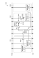
- FIG. 3 shows an example of a circuit arranged in the standard cell block SCB of FIG. 1.
- the standard cell block SCB has power domains PD1, PD2, and PD3 to which a power supply potential TVD and a ground potential VSS are supplied.
- the power supply potential TVD is an example of a second potential
- the power supply line TVD is an example of a second power supply line.
- the ground potential VSS is an example of a first potential
- the ground line VSS is an example of a first power supply line.
- the power domain PD1 has a control circuit CNTL1, a logic circuit LGC1, and a buffer BUF1 that operate on a power supply potential TVDD and a ground potential VSS.
- the power domain PD2 has buffers BUF21, BUF22, and BUF23, and a switch transistor SWT that operate on a power supply potential TVDD and a ground potential VSS that are constantly supplied.
- the power domain PD2 also has a standard cell SC that operates on a virtual power supply potential VVDD and a ground potential VSS.
- the power domain PD3 has a logic circuit LGC3 that operates by receiving a power supply potential TVDD and a ground potential VSS.
- the virtual power supply potential VVDD is an example of a third potential
- the virtual power line VVDD is an example of a third power supply line.
- Buffer BUF21 receives a control signal output from control circuit CNTL1 of power domain PD1 via buffer BUF1, and outputs it as an input signal IN to buffer BUF22.
- Buffer BUF22 has inverters IV1 and IV2 connected in series.
- Inverter IV1 receives the input signal IN and outputs an output signal OUT0 to inverter IV2 and the gate of switch transistor SWT.
- Inverter IV2 receives the output signal OUT0 and outputs an output signal OUT.
- the switch transistor SWT is a PMOS transistor with a source connected to the power supply line TVDD and a drain connected to the virtual power supply line VVDD, and operates by receiving the voltage of the output signal OUT0 output from the inverter IV1 as a gate potential. That is, the on/off of the switch transistor SWT is controlled by the control circuit CNTL1, and the supply or stop of the virtual power supply potential VVDD is switched by turning the switch transistor SWT on/off.
- the buffers BUF21 and BUF22 arranged in the power domain PD2 operate even when the switch transistor SWT is off and is not supplied with the virtual power potential VVDD. Therefore, in the power domain PD2 having the standard cell SC that operates at the virtual power potential VVDD, the on/off of the switch transistor SWT can be controlled by the control signal output from the control circuit CNTL1 of the power domain PD1.
- the standard cell SC has various logic circuits, such as, for example, a NAND circuit and an inverter.
- the standard cell SC may have an SRAM (Static Random Access Memory) or various macros.
- the buffer BUF23 receives a signal output from the logic circuit LGC1 of the power domain PD1, and outputs the received signal to the logic circuit LGC3 of the power domain PD3.
- the buffer BUF23 arranged in the power domain PD2 operates even when the switch transistor SWT is off and the virtual power supply potential VVDD is not supplied. Therefore, in the power domain PD2 having the standard cell SC that operates at the virtual power supply potential VVDD, the signal output from the logic circuit LGC1 of the power domain PD1 can be transmitted to the power domain PD3 via the BUF23 of the power domain PD2.
- the buffers BUF21, BUF22, and BUF23 that are capable of operating at all times and are arranged in the power domain PD2, which can supply and stop the virtual power potential VVDD, are sometimes called AOBs (Always on Buffers).
- the AOBs may be designed as cells.
- the AOBs are used to transmit control signals that control circuits such as the switch transistor SWT in the power domain PD2, or to transmit signals (signals not used in the power domain PD2) between other power domains such as the power domains PD1 and PD3.
- the AOBs are an example of a first circuit.
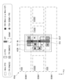
- FIG. 4 shows an example of the positional relationship between the power lines and vias arranged in the power domain PD2 of FIG. 3 in a plan view on the back side of the semiconductor substrate SUB, and the AOB.
- each wire in the wiring layer BSM1 extends in the X direction
- each wire in the wiring layer BSM2 extends in the Y direction that is different from the X direction.
- the X direction is an example of the first direction
- the Y direction is an example of the second direction.
- the symbol ROW in FIG. 4 indicates the width of the standard cell SC in the Y direction in the wiring layer BSM1.
- the virtual power lines VVDD of the wiring layer BSM1 are arranged in the Y direction at a pitch twice that of the ROW. Between a pair of virtual power lines VVDD adjacent in the Y direction, ground lines VSS extending in the X direction and interrupted at multiple points along the way, and power lines TVDD arranged at positions where the ground lines VSS are interrupted, are arranged alternately along the X direction. In other words, the power lines TVDD are arranged between multiple ground lines VSS in the X direction.
- the AOBs shown in thick dashed lines are arranged, for example, in a staggered pattern (zigzag) at positions that overlap with parts of the power supply lines TVDD and ground lines VSS in a plan view.
- standard cells SC (not shown) are arranged.
- the power supply line TVD can be arranged only in positions where the AOBs are arranged. This allows the arrangement density of the virtual power supply lines VVDD and the ground lines VSS in the wiring layer BSM1 to be increased compared to the case where a dedicated area is provided for the power supply line TVD that is wired with an interval ROW, and the power supply capacity to the standard cells SC can be increased.
- the power supply line TVD, the virtual power supply line VVDD, and the ground line VSS are repeatedly arranged in the X direction.
- the virtual power supply lines VVDD of the wiring layers BSM1 and BSM2 are connected to each other through vias VIA1 arranged at the intersections.
- the power supply lines TVD of the wiring layers BSM1 and BSM2 are connected to each other through vias VIA1 arranged at the intersections.
- the ground lines VSS of the wiring layers BSM1 and BSM2 are connected to each other through vias VIA1 arranged at the intersections.
- the virtual power line VVDD may be omitted from the wiring layer BSM2.
- the power line TVDD and the ground line VSS may be arranged alternately along the X direction in the wiring layer BSM2.
- the placement density of the AOBs is set according to the required number of AOBs to be placed in the power domain PD2.
- the cut interval of the ground lines VSS extending in the X direction in the wiring layer BSM1 may be changed, and the placement interval of the power lines TVDD in the Y direction in the wiring layer BSM1 may be changed.
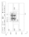
- FIG. 5 shows an example of the layout of AOB in FIG. 4.
- AOB in FIG. 5 shows buffer BUF22 in FIG. 3, but may also be buffer BUF21 or buffer BUF23 in FIG. 3.
- symbol LI indicates local wiring formed on substrate SUB.
- Wiring LI can be directly connected to the source and drain of a transistor.
- Symbol Mint indicates wiring formed in metal wiring layer Mint, which is a wiring layer on wiring LI.
- Symbol GT indicates the gate of a transistor.
- Symbol VIA indicates a via that connects Mint wiring and local wiring LI, or a via that connects Mint wiring and gate GT.
- TR(PMOS) indicates the transistor region (source, drain, and channel) of a PMOS transistor.
- TR(NMOS) indicates the transistor region (source, drain, and channel) of an NMOS transistor.
- a PMOS transistor is an example of a second transistor, and an NMOS transistor is an example of a first transistor.
- a fin is formed in the region TR.
- a semiconductor layer is formed as the source and drain in the region TR, and a nanosheet is formed as the channel between the source and drain.
- AOB is arranged in a position in the wiring layer BSM1 where it overlaps with part of the power supply line TVDD and part of the ground line VSS in a planar view.
- the NMOS transistors of inverters IV1 and IV2 included in AOB are arranged in a position where it overlaps with the ground line VSS of the wiring layer BSM1 in a planar view.
- the PMOS transistors of inverters IV1 and IV2 included in AOB are arranged in a position where it overlaps with the power supply line TVDD of the wiring layer BSM1 in a planar view.
- the sources of the NMOS transistors of inverters IV1 and IV2 are directly connected to the ground line VSS of wiring layer BSM1 via TSV.
- the sources of the PMOS transistors of inverters IV1 and IV2 are directly connected to the power supply line TVDD of wiring layer BSM1 via TSV. This allows the power supply potential TVDD and the ground potential VSS to be directly supplied to the sources of the transistors of the AOB from the back side of the substrate SUB ( Figure 2), making it possible to reduce the layout size of the AOB and arrange the AOB efficiently.
- direct connection means that the conductors contained in the TSV are in contact with the source, drain, etc. of each transistor.
- the TSV has multiple layers of conductors, it also includes cases where some of the multiple layers of conductors are in contact with the source or drain of the transistor.
- each of the power supply line TVD and ground line VSS of the wiring layer BSM1 is connected to a corresponding power supply line TVD and ground line VSS in the wiring layer BSM2 (not shown).
- the virtual power supply line VVDD of the wiring layer BSM1 may be connected to the virtual power supply line VVDD of the wiring layer BSM2.
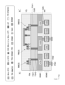
- FIG. 6 shows an example of a cross section along line X1-X1' in FIG. 5.
- the ground line VSS formed in the wiring layer BSM1 on the back surface BS side of the substrate SUB is connected to the source S (N-type impurity region) of the NMOS transistor formed on the front surface FS of the substrate SUB via a TSV1 formed in the substrate SUB.
- the power supply line TVDD formed in the wiring layer BSM1 on the back surface BS side is connected to the source S (P-type impurity region) of the PMOS transistor formed on the front surface FS via a TSV2 formed in the substrate SUB.
- each fin FIN a channel C is arranged between a source S and a drain D.
- a gate GT is arranged on the channel C via a gate insulating film (not shown).
- two wiring layers BSM1 and BSM2 are arranged on the back surface BS side, but three or more wiring layers BSM may be arranged.
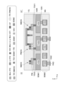
- FIG. 7 shows another example of a cross section taken along line X1-X1' in FIG. 5. Elements and layouts that are the same as or similar to those in FIG. 6 are indicated with the same symbols or the same patterns, and detailed explanations are omitted.
- FIG. 7 has the same cross-sectional structure as FIG. 6, except that the position where the wiring of the wiring layer BSM1 is formed is different.
- the wiring of the wiring layer BSM1 is formed below the substrate SUB, on the back surface BS side of the substrate SUB.
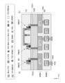
- FIG. 8 shows another example of a cross section along line X1-X1' in FIG. 5. Elements and layouts that are the same as or similar to those in FIG. 6 are indicated with the same symbols or the same patterns, and detailed descriptions are omitted.
- FIG. 8 has the same cross-sectional structure as FIG. 6, except that the position where the wiring of the wiring layer BSM1 is formed is different. The wiring of the wiring layer BSM1 is not exposed on the back surface BS side of the substrate SUB, but is formed inside the substrate SUB.
- the wiring of the wiring layer BSM1 formed in the substrate SUB is connected to the wiring of the wiring layer BSM2 through a via VIA1 formed in the substrate SUB, and is connected to the source S of the fin FIN through a via VIA3 formed in the substrate SUB.
- FIG. 9 shows yet another example of a cross section taken along line X1-X1' in FIG. 5. Elements and layouts that are the same as or similar to those in FIG. 6 are indicated with the same symbols or the same patterns, and detailed descriptions are omitted.
- FIG. 9 has the same cross-sectional structure as FIG. 6, except that the transistor formed on the substrate SUB is a nanosheet FET.
- the nanosheet FET has a semiconductor layer having a source S and a drain D, a nanosheet NS having a semiconductor material formed between the source S and the drain D, and a gate GT formed via a gate insulating film (not shown) provided on the surface of the nanosheet NS. Note that a nanosheet FET may be arranged in place of the finFET shown in FIG. 6, FIG. 7, or FIG. 8.
- FIG. 10 shows a modified layout of the AOB in FIG. 4. Elements and layouts that are the same as or similar to those in FIG. 5 are indicated with the same symbols or the same patterns, and detailed descriptions are omitted.
- the layout in FIG. 10 is similar to the layout in FIG. 5, except that an N-type well tap NWTP and a P-type well tap PWTP are arranged in regions adjacent to both sides of the AOB in the X direction.
- NWTP is an example of a first well tap
- the well tap NWTP is an example of a second well tap.
- the well tap PWTP is disposed at a position overlapping the ground line VSS of the wiring layer BSM1 in a plan view.
- the well tap PWTP is formed by a PMOS transistor whose source and drain are directly connected to the ground line VSS of the wiring layer BSM1 via a TSV. This allows the ground potential VSS to be supplied to the P-type well region PW, which is the substrate region (region other than the shaded region) of the NMOS transistor.
- the well tap NWTP is placed at a position overlapping the power supply line TVDD of the wiring layer BSM1 in a plan view.
- the well tap NWTP is formed by an NMOS transistor whose source and drain are directly connected to the power supply line TVDD of the wiring layer BSM1 via a TSV. This makes it possible to supply the power supply potential TVDD to the N-type well region NW, which is the substrate region (shaded region) of the PMOS transistor.
- the design efficiency of the circuit region can be improved.
- the sources of the NMOS transistor and PMOS transistor of the AOB are directly connected to the ground line VSS and power line TVDD of the wiring layer BSM1 via the TSV. This makes it possible to directly supply the power supply potential TVDD and the ground potential VSS to the AOB from the back side of the substrate SUB, thereby reducing the layout size of the AOB and enabling the AOB to be arranged efficiently.
- the power supply line TVD can be arranged only in positions where the AOBs are arranged. This allows the arrangement density of the virtual power supply lines VVDD and the ground line VSS in the wiring layer BSM1 to be increased compared to the case where the power supply line TVD extending in the X direction together with the virtual power supply line VVDD and the ground line VSS is arranged in the semi-circular BSM1, and the power supply capacity to the standard cells SC can be increased.
- the well tap PWTP By arranging the well tap PWTP at a position overlapping with the ground line VSS of the wiring layer BSM1 in a plan view, it is possible to supply the ground potential VSS to the P-type well region PW in which the substrate region of the NMOS transistor is located.
- the well tap NWTP By arranging the well tap NWTP at a position overlapping with the power supply line TVDD of the wiring layer BSM1 in a plan view, it is possible to supply the power supply potential TVDD to the N-type well region NW in which the substrate region of the PMOS transistor is located.
- Second Embodiment 11 shows an example of the layout of the AOB in the semiconductor device of the second embodiment.
- the same or similar elements and layout as those in FIG. 5 are indicated by the same symbols or the same patterns, and detailed description is omitted.
- the power domain PD2 shown in FIG. 11 is provided in the standard cell block SCB of FIG. 1 together with the power domains PD1 and PD3 as shown in FIG. 3.
- the ground lines VSS of the wiring layer BSM1 are formed to extend in the X direction. Between a pair of ground lines VSS adjacent to each other in the Y direction, virtual power lines VVDD extending in the X direction and interrupted at multiple points along the way, and power lines TVDD arranged at positions where the virtual power lines VVDD are interrupted are arranged alternately along the X direction. Note that the AOBs are arranged alternately (staggered) within the power domain PD2, as in FIG. 4.
- the inverters IV1 and IV2 of the AOB are arranged side by side in the Y direction.
- the NMOS transistors of the inverters IV1 and IV2 are arranged in a position overlapping the ground line VSS of the wiring layer BSM1 in a planar view.
- the PMOS transistors of the inverters IV1 and IV2 are arranged in a position overlapping the power supply line TVD of the wiring layer BSM1 in a planar view.
- FIG. 12 shows a modified layout of the AOB in FIG. 11. Elements and layouts that are the same as or similar to those in FIG. 11 are indicated with the same symbols or the same patterns, and detailed descriptions are omitted.
- the AOB is arranged across the boundary between the power supply line TVDD and the ground line VSS in the wiring layer BSM1, and the inverters IV1 and IV2 are arranged side by side in the X direction.
- the NMOS transistors of the inverters IV1 and IV2 are arranged in a position that overlaps with the ground line VSS of the wiring layer BSM1 in a plan view.
- the PMOS transistors of the inverters IV1 and IV2 are arranged in a position that overlaps with the power supply line TVDD of the wiring layer BSM1 in a plan view.
- the sources of the PMOS transistors of the inverters IV1 and IV2 are common and connected to the power supply line TVDD of the wiring layer BSM1 via a common TSV.
- the sources of the NMOS transistors of the inverters IV1 and IV2 are common and connected to the ground line VSS of the wiring layer BSM1 via a common TSV.
- the source of the PMOS transistor can be directly connected to the power supply line TVDD of the wiring layer BSM1 via the TSV, and the source of the NMOS transistor can be directly connected to the ground line VSS of the wiring layer BSM1 via the TSV. Furthermore, by sharing the TSV, it becomes possible to make the layout size of the AOB smaller than those of FIG. 5 and FIG. 11.
- the sources of the PMOS transistors of the inverters IV1 and IV2 may be provided independently of each other, and the sources of the NMOS transistors of the inverters IV1 and IV2 may be provided independently of each other. In other embodiments and modifications, the sources of the PMOS transistors of the inverters IV1 and IV2 may be shared, and the sources of the NMOS transistors of the inverters IV1 and IV2 may be shared.
- the second embodiment can also achieve the same effects as the first embodiment.
- the power supply potential TVDD and the ground potential VSS can be directly supplied to the AOB from the back side of the substrate SUB, and the layout size of the AOB can be reduced and the AOB can be efficiently arranged.
- the power supply line TVDD is arranged at a position where the virtual power supply line VVDD extending in the X direction is interrupted, the power supply potential TVDD and the ground potential VSS can be directly supplied to the AOB from the back side of the substrate SUB.
- the sources of the PMOS transistors of the inverters IV1 and IV2 are common and connected to the power supply line TVDD of the wiring layer BSM1 via a common TSV.
- the sources of the NMOS transistors of the inverters IV1 and IV2 are common and connected to the ground line VSS of the wiring layer BSM1 via a common TSV. This allows the layout size of the AOB to be further reduced, and the AOB to be arranged more efficiently.
- Third Embodiment 13 shows an example of the positional relationship between the AOB and the power supply lines and vias arranged at positions overlapping the standard cell blocks in FIG. 3 in a plan view in the semiconductor device of the third embodiment. Elements and layouts that are the same as or similar to those in FIG. 4 are indicated by the same symbols or patterns, and detailed descriptions thereof will be omitted.
- the power domain PD2 shown in FIG. 13 is provided in the standard cell block SCB in FIG. 1 together with the power domains PD1 and PD3 as shown in FIG. 3.
- the power wiring in the wiring layer BSM1 is not interrupted, and the ground line VSS, power line TVDD, and virtual power line VVDD extending in the X direction are arranged side by side in the Y direction.
- the AOB is arranged at a position overlapping the ground line VSS and power line TVDD adjacent to each other in the wiring layer BSM1.
- FIG. 14 shows an example of the layout of the AOB in FIG. 13. Elements and layouts that are the same as or similar to those in FIG. 5 are indicated with the same symbols or the same patterns, and detailed descriptions are omitted.
- the layout of the AOB shown in FIG. 4 is the same as or similar to the layout of the AOB in FIG. 12. That is, the AOB is arranged across the boundary between the power supply line TVDD and the ground line VSS in the wiring layer BSM1, and the inverters IV1 and IV2 are arranged side by side in the X direction.
- the sources of the PMOS transistors of the inverters IV1 and IV2 are common and connected to the power supply line TVDD of the wiring layer BSM1 via a common TSV.
- the sources of the NMOS transistors of the inverters IV1 and IV2 are common and connected to the ground line VSS of the wiring layer BSM1 via a common TSV.
- the sources of the PMOS transistors of the inverters IV1 and IV2 may be provided independently of each other. Also, the sources of the NMOS transistors of the inverters IV1 and IV2 may be provided independently of each other.
- the third embodiment can achieve the same effects as the first embodiment.
- the power supply potential TVDD and the ground potential VSS can be directly supplied to the AOB from the back surface side of the substrate SUB, and the layout size of the AOB can be reduced and the AOB can be arranged efficiently.
- the layout size of the AOB can be reduced and the AOB can be arranged efficiently.
- FIG. 15 shows an example of the layout of the AOB in the semiconductor device of the fourth embodiment.
- the same or similar elements and layout as those in Fig. 5 are indicated by the same symbols or the same patterns, and detailed description is omitted.
- the power domain PD2 shown in Fig. 15 is provided in the standard cell block SCB of Fig. 1 together with the power domains PD1 and PD3 as shown in Fig. 3.
- the layout of the ground line VSS, virtual power line VVDD, and power line TVDD of the wiring layer BSM1 in FIG. 15 is the same as that in FIG. 11. That is, the ground line VSS is formed extending in the X direction. Between a pair of ground lines VSS adjacent to each other in the Y direction, a virtual power line VVDD that extends in the X direction and is interrupted at multiple points along the way, and a power line TVDD that is arranged at the position where the virtual power line VVDD is interrupted are arranged alternately along the X direction.
- the power tap cell TPC is placed at a position overlapping the virtual power line VVDD of the wiring layer BSM1 in a planar view.
- two AOB1 and AOB2 are placed side by side in the X direction at positions overlapping the power line TVDD and the ground line VSS of the wiring layer BSM1 in a planar view.
- the power tap cell TPC has a PMOS transistor whose source and drain are directly connected to the power line TVDD of the wiring layer BSM1 via a TSV.
- the power tap cell TPC also has a PMOS transistor whose source and drain are directly connected to the ground line VSS of the wiring layer BSM1 via a TSV.
- the source and drain of a transistor are an example of a semiconductor layer.
- the inverters IV1 and IV2 of each of AOB1 and AOB2 are arranged side by side in the Y direction, as in FIG. 11.
- the PMOS transistors of the inverters IV1 and IV2 are arranged in a position overlapping the power line TVDD of the wiring layer BSM1 in a plan view.
- the sources of the PMOS transistors of each of AOB1 and AOB2 are connected to the source and drain of the PMOS transistor of the power tap cell TPC via the Mint wiring extending in the Y direction, the via VIA, and the local wiring LI extending in the X direction. That is, each of AOB1 and AOB2 receives the power supply potential TVDD supplied from the power tap cell TPC.
- the NMOS transistors of inverters IV1 and IV2 are arranged in a position overlapping the ground line VSS of wiring layer BSM1 in a plan view, and the sources of the NMOS transistors are directly connected to the ground line VSS of wiring layer BSM1 via TSVs.
- a power tap cell TPC is arranged at a position corresponding to the power line TVDD of the wiring layer BSM1, and the power tap cell TPC supplies a power supply potential TVDD to multiple AOB1 and AOB2.
- AOC to be placed not only in a position opposite the power line TVDD of the wiring layer BSM1, but also in a position opposite the virtual power line VVDD of the wiring layer BSM1.
- the number of power lines TVDD of the wiring layer BSM1 can be reduced, and the area occupied by free space in the circuit area can be reduced. This makes it possible to suppress an increase in the element area.
- the power line TVDD of the wiring layer BSM1 is placed in a position corresponding to each of AOB1 and AOB2, free space is required for the power line TVDD corresponding to each of AOB1 and AOB2, which may increase the element area.
- the fourth embodiment can also achieve the same effects as the first embodiment.
- the power supply potential TVDD and the ground potential VSS can be directly supplied to the AOB from the back side of the substrate SUB, and the layout size of the AOB can be reduced, allowing the AOB to be arranged efficiently.
- the power tap cell TPC arranged at a position overlapping the power line TVDD of the wiring layer BSM1 in a plan view is connected to the sources of the PMOS transistors of the multiple AOBs via wiring.
- This allows the number of power lines TVDD of the wiring layer BSM1 to be reduced compared to the case where the power line TVDD of the wiring layer BSM1 is arranged for each AOB, and the area occupied by free space in the circuit area can be reduced.
- the power line TVDD of the wiring layer BSM1 is arranged at a position where the virtual power line VVDD is interrupted, but even if the power line TVDD is arranged at a position where the ground line VSS of the wiring layer BSM1 is interrupted, the power tap cell TPC may supply the power potential TVDD to the multiple AOB1 and AOB2. Also, a similar configuration may be used in other embodiments.
- FIG. 16 shows an example of a circuit arranged in a standard cell block SCB in a semiconductor device according to the fifth embodiment. Elements that are the same as or similar to those in Fig. 3 are given the same reference numerals, and detailed description thereof will be omitted.
- the standard cell block SCB shown in Fig. 16 is mounted in the internal circuit region INTR of the semiconductor device 100, similar to that in Fig. 1.
- the standard cell block SCB shown in FIG. 16 has power domains PD1 and PD3 to which a power supply potential TVDD and a ground potential are supplied, and a power domain PD2 to which a power supply potential VVDD and a ground potential VSS are supplied, similar to FIG. 3.
- the power domains PD1 and PD3 are the same as the power domains PD1 and PD3 in FIG. 3, respectively.
- the power domain PD2 does not have the switch transistor SWT included in the power domain PD2 of FIG. 3.
- a virtual power supply potential VVDD supplied from a power supply management IC (Integrated Circuit) provided outside the semiconductor device 100 is supplied to a virtual power supply line VVDD in the power domain PD2 via a switch SW.
- the power supply management IC may be disposed on the board on which the semiconductor device 100 is mounted, or may be disposed outside the board on which the semiconductor device 100 is mounted.
- the buffer BUF22 is used to control the circuit of the power domain PD2 or the circuit of the power domain PD3.
- the layout and cross-sectional structure of the AOBs such as the buffers BUF21, BUF22, and BUF23 are the same as or similar to the layout and cross-sectional structure of the AOBs in the first to fourth embodiments.
- the fifth embodiment can also achieve the same effects as the first to fourth embodiments.
Landscapes
- Engineering & Computer Science (AREA)
- Power Engineering (AREA)
- Design And Manufacture Of Integrated Circuits (AREA)
- Semiconductor Integrated Circuits (AREA)
Abstract
半導体装置は、基板の上面より下方に形成された第1の電源線と第2の電源線と第3の電源線と、基板の上方に形成され、第1の電源線と平面視で重なって配置された第1のトランジスタと、基板の上方に形成された第2のトランジスタと、基板に形成され、第1のトランジスタのソースと第1の電源線とを接続する第1のビアとを有する。これにより、ソース、ドレインがビアを介して基板の上面より下方の配線に直接接続されるトランジスタを含むバッファを効率よく配置することができる。
Description
本発明は、半導体装置に関する。
半導体装置において、電源スイッチ回路等の制御により電源電位の供給又は供給の停止が可能な電源ドメインにおいて、常に動作する回路を設ける技術が知られている。常に動作する回路がバッファである場合、Always on Buffer(以下AOB)と呼ばれる。
半導体基板の裏面に形成された配線から、半導体の表面に形成されたトランジスタ等の素子に電源電位を供給するBS-PDN(Backside Power Delivery Network)技術が知られている。半導体基板の表面のトランジスタのソース、ドレインに、半導体基板の下方からビアを直接接続する技術が知られている。
半導体基板の表面のトランジスタのソース、ドレインに直接ビアを接続する技術をAOBに適用した場合に、配線及びビア等をどのように配置し、接続するのか具体的に検討がされていない。
本発明は、上記の点に鑑みてなされたもので、ソース、ドレインがビアを介して基板の下方の配線に直接接続されるトランジスタを含むバッファを効率よく配置することを目的とする。
本発明の一態様では、半導体装置は、基板と、前記基板の下方に形成され、第1の電位が供給される第1の電源線と、第2の電位が供給される第2の電源線と、第3の電位が供給される第3の電源線と、前記基板の上方に形成され、前記第1の電源線と平面視で重なって配置された第1のトランジスタと、前記基板の上方に形成された第2のトランジスタと、前記基板に形成され、前記第1のトランジスタのソースと前記第1の電源線とを接続する第1のビアと、を有する。
開示の技術によれば、ソース、ドレインがビアを介して基板の下方の配線に直接接続されるトランジスタを含むバッファを効率よく配置することができる。
以下、図面を用いて実施形態を説明する。以下では、信号を示す符号は、信号線又は信号端子を示す符号としても使用される。電源電位を示す符号は、電源電位が供給される電源線又は電源端子を示す符号としても使用される。
(第1実施形態)
図1は、第1実施形態における半導体装置のレイアウトの一例を示す。例えば、図1に示す半導体装置100は、SoC(System on Chip)でもよく、単体のFPGA(Field-Programmable Gate Array)等でもよい。
図1は、第1実施形態における半導体装置のレイアウトの一例を示す。例えば、図1に示す半導体装置100は、SoC(System on Chip)でもよく、単体のFPGA(Field-Programmable Gate Array)等でもよい。
半導体装置100は、複数のI/OセルIOC、IOCPと内部回路領域INTRとを有する。I/OセルIOCは、入力信号、出力信号又は入出力信号等の信号SGNL用のインタフェース回路である。I/OセルIOCPは、電源電位又は接地電位用のインタフェース回路である。
各I/OセルIOC、IOCPは、内部回路領域INTRに接続される。例えば、内部回路領域INTRは、スタンダードセルが設けられる1つ又は複数のスタンダードセルブロックSCBを有する。なお、内部回路領域INTRには、スタンダードセル以外の論理回路が搭載されてもよく、メモリが搭載されてもよい。メモリは、スタンダードセルブロックSCB内に搭載されてもよい。
図2は、図1の半導体装置100の断面構造の一例を示す。半導体装置100は、基板SUBと、基板SUBの表面FS側に形成された配線層WL1と、基板SUBの裏面BS側に形成された配線層WL2とを有する。基板SUBの表面FSは、基板SUBの上面又は基板SUBの上方の一例であり、基板SUBの裏面BSは、基板SUBの下方の一例である。基板SUBの表面には、トランジスタの一部であるフィンFINが形成される。フィンFINは、ソース、ドレイン及びチャネルを有する。配線層WL2における基板SUBと反対側の面(裏面)には、外部接続端子であるパッドPADが形成される。
配線層WL2は、複数の配線層BSM1、BSM2(図2では2層、BSMはBackside Metalの略)を有する。例えば、配線層BSM1、BSM2には、電源電位及び接地電位等をそれぞれ供給する配線W1、W2がそれぞれ形成される。配線W1、W2は、ビアVIA1を介して相互に接続される。配線W2とパッドPADとは、ビアVIA2を介して相互に接続される。
配線W1は、基板SUBに形成されたTSV(Through Silicon Via)を介してフィンFINのソース及びドレインに接続される。配線W1は、TSVを介して、基板SUBの表面に埋め込まれた埋め込み配線BPR(Buried Power Rail)に接続されてもよい。TSVは、ビアの一例である。
なお、基板SUB上に形成されるトランジスタは、フィンを用いたフィンFET(Field Effect Transistor)に限られない。例えば、基板SUB上に形成されるトランジスタは、プレーナ型MOSFET(Metal Oxide Semiconductor FET)、ナノシートFET又はCFET(Complementary FET)でもよい。
プレーナ型MOSFET及びナノシートFETにおいても、電源電位又は接地電位を供給するTSVは、トランジスタのソース及びドレインに接続される。また、CFETの場合、電源電位又は接地電位を供給するTSVは、基板SUBの最も近くに位置するソース及びドレインに接続されてもよい。
図3は、図1のスタンダードセルブロックSCBに配置される回路の一例を示す。図3に示す例では、スタンダードセルブロックSCBは、電源電位TVDD及び接地電位VSSが供給される電源ドメインPD1、PD2、PD3を有する。電源電位TVDDは、第2の電位の一例であり、電源線TVDDは、第2の電源線の一例である。接地電位VSSは、第1の電位の一例であり、接地線VSSは、第1の電源線の一例である。
電源ドメインPD1は、電源電位TVDD及び接地電位VSSを受けて動作する制御回路CNTL1、論理回路LGC1及びバッファBUF1を有する。電源ドメインPD2は、常時供給される電源電位TVDDと接地電位VSSとを受けて動作するバッファBUF21、BUF22、BUF23及びスイッチトランジスタSWTを有する。また、電源ドメインPD2は、仮想電源電位VVDDと接地電位VSSとを受けて動作するスタンダードセルSCとを有する。
電源ドメインPD3は、電源電位TVDD及び接地電位VSSを受けて動作する論理回路LGC3を有する。仮想電源電位VVDDは、第3の電位の一例であり、仮想電源線VVDDは、第3の電源線の一例である。
バッファBUF21は、電源ドメインPD1の制御回路CNTL1から出力される制御信号をバッファBUF1を介して受け、入力信号INとしてバッファBUF22に出力する。バッファBUF22は、直列に接続されたインバータIV1、IV2を有する。インバータIV1は、入力信号INを受けて出力信号OUT0をインバータIV2及びスイッチトランジスタSWTのゲートに出力する。インバータIV2は、出力信号OUT0を受けて出力信号OUTを出力する。
スイッチトランジスタSWTは、ソースが電源線TVDDに接続され、ドレインが仮想電源線VVDDに接続されたPMOSトランジスタであり、インバータIV1から出力される出力信号OUT0の電圧をゲート電位として受けて動作する。すなわち、スイッチトランジスタSWTのオン/オフは、制御回路CNTL1により制御され、仮想電源電位VVDDの供給又は停止は、スイッチトランジスタSWTのオン/オフにより切り替えられる。
電源ドメインPD2に配置されるバッファBUF21、BUF22は、仮想電源電位VVDDが供給されないスイッチトランジスタSWTのオフ中にも動作する。このため、仮想電源電位VVDDで動作するスタンダードセルSCを有する電源ドメインPD2において、電源ドメインPD1の制御回路CNTL1から出力される制御信号によりスイッチトランジスタSWTのオン/オフを制御することができる。
スイッチトランジスタSWTがオンしている間、電源線TVDDと仮想電源線VVDDとが電気的に接続され、電源電位TVDDは、仮想電源線VVDDを介してスタンダードセルSCに供給される。スイッチトランジスタSWTがオフしている間、電源線TVDDと仮想電源線VVDDとの電気的な接続が遮断され、仮想電源線VVDDは、フローティング状態に設定される。スタンダードセルSCは、例えば、NAND回路及びインバータ等の各種論理回路を有する。スタンダードセルSCは、SRAM(Static Random Access Memory)又は各種マクロを有してもよい。
バッファBUF23は、電源ドメインPD1の論理回路LGC1から出力される信号を受け、受けた信号を電源ドメインPD3の論理回路LGC3に出力する。電源ドメインPD2に配置されるバッファBUF23は、仮想電源電位VVDDが供給されないスイッチトランジスタSWTのオフ中にも動作する。このため、仮想電源電位VVDDで動作するスタンダードセルSCを有する電源ドメインPD2において、電源ドメインPD1の論理回路LGC1から出力される信号を電源ドメインPD2のBUF23を介して電源ドメインPD3へ伝達することができる。
仮想電源電位VVDDの供給と停止とが可能な電源ドメインPD2内に配置される常時動作が可能なバッファBUF21、BUF22、BUF23は、AOB(Always on Buffer)と呼ばれることがある。例えば、AOBは、セルとして設計されてもよい。AOBは、電源ドメインPD2内のスイッチトランジスタSWT等の回路を制御する制御信号の伝達、又は、電源ドメインPD1、PD3等の他の電源ドメイン間での信号(電源ドメインPD2では使用されない信号)の伝達に使用される。AOBは、第1の回路の一例である。
図4は、半導体基板SUBの裏面側において、平面視で図3の電源ドメインPD2に配置される電源線及びビアと、AOBとの位置関係の一例を示す。例えば、配線層BSM1の各配線は、X方向に延在し、配線層BSM2の各配線は、X方向と異なるY方向に延在している。X方向は、第1の方向の一例であり、Y方向は、第2の方向の一例である。図4に示す符号ROWは、配線層BSM1におけるY方向のスタンダードセルSCの幅を示す。
配線層BSM1の仮想電源線VVDDは、Y方向にROWの2倍のピッチで配置される。Y方向に隣接する一対の仮想電源線VVDDの間には、X方向に延在し、途中の複数個所で途切れている接地線VSSと、接地線VSSが途切れた位置に配置された電源線TVDDとが、X方向に沿って交互に配置される。換言すると、X方向において複数の接地線VSSの間に電源線TVDDが配置される。
太い破線枠で示すAOBは、平面視で電源線TVDDの一部と接地線VSSの一部とに重なる位置に、例えば、互い違い(千鳥状)に配置される。AOBが配置されない領域には、例えば、図示しないスタンダードセルSCが配置される。
電源線TVDDを接地線VSSの途切れた位置に分散して配置することで、配線層BSM1において仮想電源線VVDD及び接地線VSSとともにX方向に延在する電源線TVDD用の配置を不要にすることができる。また、電源線TVDDをAOBが配置される位置のみに配置することができる。これにより、間隔ROWを空けて配線される電源線TVDD用の専用の領域を設ける場合に比べて、配線層BSM1における仮想電源線VVDD及び接地線VSSの配置密度を高くすることができ、スタンダードセルSCへの電源供給能力を高くすることができる。
配線層BSM2では、電源線TVDD、仮想電源線VVDD及び接地線VSSが、X方向に繰り返し配置される。配線層BSM1、BSM2の仮想電源線VVDDは、交差部分に配置されるビアVIA1を介して相互に接続される。配線層BSM1、BSM2の電源線TVDDは、交差部分に配置されるビアVIA1を介して相互に接続される。配線層BSM1、BSM2の接地線VSSは、交差部分に配置されるビアVIA1を介して相互に接続される。
なお、仮想電源線VVDDは、配線層BSM2での配置が省略されてもよい。この場合、配線層BSM2において、電源線TVDDと接地線VSSとがX方向に沿って交互に配置されてもよい。
なお、AOBの配置密度は、電源ドメインPD2内に配置するAOBの必要数に応じて設定される。この場合、配線層BSM1でX方向に延在する接地線VSSの切断間隔が変えられてもよく、配線層BSM1のY方向における電源線TVDDの配置間隔が変えられてもよい。
図5は、図4のAOBのレイアウトの一例を示す。図5に示すAOBは、図3のバッファBUF22を示すが、図3のバッファBUF21又はバッファBUF23でもよい。図5及び以降の平面図に示す凡例において、符号LIは、基板SUB上に形成されたローカル配線を示す。配線LIは、トランジスタのソース及びドレインと直接接続が可能である。符号Mintは、配線LI上の配線層である金属配線層Mintに形成された配線を示す。符号GTは、トランジスタのゲートを示す。符号VIAは、Mint配線とローカル配線LIとを接続するビア、又はMint配線とゲートGTとを接続するビアを示す。
符号TR(PMOS)は、PMOSトランジスタのトランジスタ領域(ソース、ドレイン及びチャネル)を示す。符号TR(NMOS)は、NMOSトランジスタのトランジスタ領域(ソース、ドレイン及びチャネル)を示す。PMOSトランジスタは、第2のトランジスタの一例であり、NMOSトランジスタは、第1のトランジスタの一例である。
例えば、フィンFETでは、領域TRにフィンが形成される。ナノシートFETでは、領域TRにソース及びドレインとして半導体層が形成され、ソース及びドレインの間にチャネルであるナノシートが形成される。
AOBは、図4に示したように、配線層BSM1において平面視で電源線TVDDの一部と接地線VSSの一部とに重なる位置に配置される。AOBに含まれるインバータIV1、IV2のNMOSトランジスタは、平面視で配線層BSM1の接地線VSSに重なる位置に配置される。AOBに含まれるインバータIV1、IV2のPMOSトランジスタは、平面視で配線層BSM1の電源線TVDDに重なる位置に配置される。
インバータIV1、IV2のNMOSトランジスタのソースは、TSVを介して配線層BSM1の接地線VSSに直接接続される。インバータIV1、IV2のPMOSトランジスタのソースは、TSVを介して配線層BSM1の電源線TVDDに直接接続される。これにより、基板SUB(図2)の裏面側からAOBのトランジスタのソースに電源電位TVDD及び接地電位VSSを直接供給することができ、AOBのレイアウトサイズを小さくして、AOBを効率よく配置することができる。
なお、直接接続とは、TSVに含まれる導電体が各トランジスタのソースやドレイン等に接していることを意味し、例えばTSVが複数層の導電体を有する場合にその複数層の導電体の一部がトランジスタのソースやドレインに接していることも含まれる。
なお、配線層BSM1の電源線TVDD及び接地線VSSの各々は、図示を省略した配線層BSM2において対応する電源線TVDD及び接地線VSSの各々に接続される。また、配線層BSM2に仮想電源線VVDDが配置される場合、配線層BSM1の仮想電源線VVDDは、配線層BSM2の仮想電源線VVDDと接続されてもよい。
図6は、図5のX1-X1'線に沿う断面の一例を示す。基板SUBの裏面BS側の配線層BSM1に形成された接地線VSSは、基板SUBに形成されたTSV1を介して基板SUBの表面FS上に形成されたNMOSトランジスタのソースS(N型不純物領域)に接続される。同様に、裏面BS側の配線層BSM1に形成された電源線TVDDは、基板SUBに形成されたTSV2を介して、表面FS上に形成されたPMOSトランジスタのソースS(P型不純物領域)に接続される。
各フィンFINにおいて、ソースSとドレインDとの間には、チャネルCが配置される。チャネルCの上には、ゲート絶縁膜(図示せず)を介してゲートGTが配置される。なお、図6では、裏面BS側に2つの配線層BSM1、BSM2が配置されるが、3層以上の配線層BSMが配置されてもよい。
図7は、図5のX1-X1'線に沿う断面の別の例を示す。図6と同一又は同様の要素及びレイアウトについては、同じ符号又は同じパターンで示し、詳細な説明は省略する。図7は、配線層BSM1の配線が形成される位置が異なることを除き、図6の断面構造と同様である。配線層BSM1の配線は、基板SUBの下方であって基板SUB中の裏面BS側に形成される。
図8は、図5のX1-X1'線に沿う断面の別の例を示す。図6と同一又は同様の要素及びレイアウトについては、同じ符号又は同じパターンで示し、詳細な説明は省略する。図8は、配線層BSM1の配線が形成される位置が異なることを除き、図6の断面構造と同様である。配線層BSM1の配線は、基板SUBの裏面BS側に露出せず、基板SUBの内部に形成される。基板SUB中に形成される配線層BSM1の配線は、基板SUBに形成されたビアVIA1を介して、配線層BSM2の配線に接続され、基板SUBに形成されたビアVIA3を介して、フィンFINのソースSに接続される。
図9は、図5のX1-X1'線に沿う断面のさらなる別の例を示す。図6と同一又は同様の要素及びレイアウトについては、同じ符号又は同じパターンで示し、詳細な説明は省略する。図9は、基板SUB上に形成されるトランジスタがナノシートFETであることを除き、図6の断面構造と同様である。ナノシートFETは、ソースS及びドレインDを有する半導体層と、ソースS及びドレインDの間に形成された半導体材料を有するナノシートNSと、ナノシートNSの表面に設けられるゲート絶縁膜(図示せず)を介して形成されたゲートGTとを有する。なお、図6、図7又は図8に示すフィンFETの代わりにナノシートFETが配置されてもよい。
図10は、図4のAOBのレイアウトの変形例を示す。図5と同一又は同様の要素及びレイアウトについては、同じ符号又は同じパターンで示し、詳細な説明は省略する。図10のレイアウトは、AOBのX方向の両側に隣接する領域にN型のウェルタップNWTPとP型のウェルタップPWTPとが配置されることを除き、図5のレイアウトと同様である。ウェルタップPWTPは、第1のウェルタップの一例であり、ウェルタップNWTPは、第2のウェルタップの一例である。
ウェルタップPWTPは、平面視で配線層BSM1の接地線VSSと重なる位置に配置される。ウェルタップPWTPは、ソース及びドレインがTSVを介して配線層BSM1の接地線VSSに直接接続されたPMOSトランジスタにより形成される。これにより、NMOSトランジスタの基板領域(網掛け以外の領域)であるP型のウェル領域PWに接地電位VSSを供給することができる。
ウェルタップNWTPは、平面視で配線層BSM1の電源線TVDDと重なる位置に配置される。ウェルタップNWTPは、ソース及びドレインがTSVを介して配線層BSM1の電源線TVDDに直接接続されたNMOSトランジスタにより形成される。これにより、PMOSトランジスタの基板領域(網掛けの領域)であるN型のウェル領域NWに電源電位TVDDを供給することができる。図10に示すように、AOBを配置する領域に隣接してウェルタップNWTP、PWTPを配置することで、回路領域の設計効率を向上することができる。
以上、第1実施形態では、AOBのNMOSトランジスタ及びPMOSトランジスタのソースを、TSVを介して配線層BSM1の接地線VSS及び電源線TVDDに直接接続する。これにより、基板SUBの裏面側からAOBに電源電位TVDD及び接地電位VSSを直接供給することができ、AOBのレイアウトサイズを小さくして、AOBを効率よく配置することができる。
電源線TVDDを接地線VSSの途切れた位置に分散して配置することで、配線層BSM1において仮想電源線VVDD及び接地線VSSとともにX方向に延在する電源線TVDD用の配置を不要にすることができる。また、電源線TVDDをAOBが配置される位置のみに配置することができる。これにより、仮想電源線VVDD及び接地線VSSとともにX方向に延在する電源線TVDDを半戦争BSM1に配置する場合に比べて、配線層BSM1における仮想電源線VVDD及び接地線VSSの配置密度を高くすることができ、スタンダードセルSCへの電源供給能力を高くすることができる。
ウェルタップPWTPを平面視で配線層BSM1の接地線VSSと重なる位置に配置することで、NMOSトランジスタの基板領域があるP型のウェル領域PWに接地電位VSSを供給することができる。ウェルタップNWTPを平面視で配線層BSM1の電源線TVDDと重なる位置に配置することで、PMOSトランジスタの基板領域あるN型のウェル領域NWに電源電位TVDDを供給することができる。
(第2実施形態)
図11は、第2実施形態の半導体装置におけるAOBのレイアウトの一例を示す。図5と同一又は同様の要素及びレイアウトについては、同じ符号又は同じパターンで示し、詳細な説明は省略する。例えば、図11に示す電源ドメインPD2は、図3に示したように、電源ドメインPD1、PD3とともに図1のスタンダードセルブロックSCBに設けられる。
図11は、第2実施形態の半導体装置におけるAOBのレイアウトの一例を示す。図5と同一又は同様の要素及びレイアウトについては、同じ符号又は同じパターンで示し、詳細な説明は省略する。例えば、図11に示す電源ドメインPD2は、図3に示したように、電源ドメインPD1、PD3とともに図1のスタンダードセルブロックSCBに設けられる。
図11では、配線層BSM1の接地線VSSは、X方向に延在して形成される。Y方向に互いに隣接する一対の接地線VSSの間には、X方向に延在し、途中の複数個所で途切れている仮想電源線VVDDと、仮想電源線VVDDが途切れた位置に配置された電源線TVDDとが、X方向に沿って交互に配置される。なお、AOBは、図4と同様に、電源ドメインPD2内において互い違い(千鳥状)に配置される。
配線層BSM1において電源線TVDDと接地線VSSとがY方向に並んで配置される場合、AOBのインバータIV1、IV2は、Y方向に並んで配置される。そして、インバータIV1、IV2のNMOSトランジスタは、平面視で配線層BSM1の接地線VSSに重なる位置に配置される。インバータIV1、IV2のPMOSトランジスタは、平面視で配線層BSM1の電源線TVDDに重なる位置に配置される。これにより、図5と同様に、NMOSトランジスタのソースをTSVを介して配線層BSM1の接地線VSSに直接接続することができ、PMOSトランジスタのソースをTSVを介して配線層BSM1の電源線TVDDに直接接続することができる。
図12は、図11のAOBのレイアウトの変形例を示す。図11と同一又は同様の要素及びレイアウトについては、同じ符号又は同じパターンで示し、詳細な説明は省略する。図12では、AOBは、配線層BSM1における電源線TVDDと接地線VSSとの境界部分を跨いで配置され、インバータIV1、IV2は、X方向に並んで配置される。インバータIV1、IV2のNMOSトランジスタは、平面視で配線層BSM1の接地線VSSに重なる位置に配置される。インバータIV1、IV2のPMOSトランジスタは、平面視で配線層BSM1の電源線TVDDに重なる位置に配置される。
インバータIV1、IV2のPMOSトランジスタのソースは、共通化され、共通のTSVを介して配線層BSM1の電源線TVDDに接続される。インバータIV1、IV2のNMOSトランジスタのソースは、共通化され、共通のTSVを介して配線層BSM1の接地線VSSに接続される。
これにより、図5と同様に、PMOSトランジスタのソースをTSVを介して配線層BSM1の電源線TVDDに直接接続することができ、NMOSトランジスタのソースをTSVを介して配線層BSM1の接地線VSSに直接接続することができる。また、TSVを共通化することで、AOBのレイアウトサイズを図5及び図11に比べて小さくすることが可能になる。
なお、インバータIV1、IV2のPMOSトランジスタのソースは、互いに独立に設けられてもよく、インバータIV1、IV2のNMOSトランジスタのソースは、互いに独立に設けられてもよい。また、他の実施形態および変形例において、インバータIV1、IV2のPMOSトランジスタのソースが共通化され、インバータIV1、IV2のNMOSトランジスタのソースが共通化されてもよい。
以上、第2実施形態においても、第1実施形態と同様の効果を得ることができる。例えば、基板SUBの裏面側からAOBに電源電位TVDD及び接地電位VSSを直接供給することができ、AOBのレイアウトサイズを小さくして、AOBを効率よく配置することができる。また、X方向に延在する仮想電源線VVDDが途切れた位置に電源線TVDDが配置される場合にも、基板SUBの裏面側からAOBに電源電位TVDD及び接地電位VSSを直接供給することができる。
さらに、インバータIV1、IV2のPMOSトランジスタのソースは、共通化され、共通のTSVを介して配線層BSM1の電源線TVDDに接続される。インバータIV1、IV2のNMOSトランジスタのソースは、共通化され、共通のTSVを介して配線層BSM1の接地線VSSに接続される。これにより、AOBのレイアウトサイズをさらに小さくして、AOBをさらに効率よく配置することができる。
(第3実施形態)
図13は、第3実施形態の半導体装置において、平面視で図3のスタンダードセルブロックと重なる位置に配置される電源線及びビアと、AOBとの位置関係の一例を示す。図4と同一又は同様の要素及びレイアウトについては、同じ符号又は同じパターンで示し、詳細な説明は省略する。
図13は、第3実施形態の半導体装置において、平面視で図3のスタンダードセルブロックと重なる位置に配置される電源線及びビアと、AOBとの位置関係の一例を示す。図4と同一又は同様の要素及びレイアウトについては、同じ符号又は同じパターンで示し、詳細な説明は省略する。
例えば、図13に示す電源ドメインPD2は、図3に示したように、電源ドメインPD1、PD3とともに図1のスタンダードセルブロックSCBに設けられる。この実施形態では、配線層BSM1の電源配線が途切れておらず、X方向に延在する接地線VSS、電源線TVDD及び仮想電源線VVDDがY方向に並んで配置される。AOBは、配線層BSM1において互いに隣接する接地線VSSと電源線TVDDとに重なる位置に配置される。
図14は、図13のAOBのレイアウトの一例を示す。図5と同一又は同様の要素及びレイアウトについては、同じ符号又は同じパターンで示し、詳細な説明は省略する。図4に示すAOBのレイアウトは、図12のAOBのレイアウトと同一又は同様である。すなわち、AOBは、配線層BSM1における電源線TVDDと接地線VSSとの境界部分を跨いで配置され、インバータIV1、IV2は、X方向に並んで配置される。
インバータIV1、IV2のPMOSトランジスタのソースは、共通化され、共通のTSVを介して配線層BSM1の電源線TVDDに接続される。インバータIV1、IV2のNMOSトランジスタのソースは、共通化され、共通のTSVを介して配線層BSM1の接地線VSSに接続される。
なお、インバータIV1、IV2のPMOSトランジスタのソースは、互いに独立に設けられてもよい。また、インバータIV1、IV2のNMOSトランジスタのソースは、互いに独立に設けられてもよい。
以上、第3実施形態においても、第1実施形態と同様の効果を得ることができる。例えば、基板SUBの裏面側からAOBに電源電位TVDD及び接地電位VSSを直接供給することができ、AOBのレイアウトサイズを小さくして、AOBを効率よく配置することができる。また、配線層BSM1の電源線TVDDがX方向に延在して配置される場合にも、AOBのレイアウトサイズを小さくして、AOBを効率よく配置することができる。
(第4実施形態)
図15は、第4実施形態の半導体装置におけるAOBのレイアウトの一例を示す。図5と同一又は同様の要素及びレイアウトについては、同じ符号又は同じパターンで示し、詳細な説明は省略する。例えば、図15に示す電源ドメインPD2は、図3に示したように、電源ドメインPD1、PD3とともに図1のスタンダードセルブロックSCBに設けられる。
図15は、第4実施形態の半導体装置におけるAOBのレイアウトの一例を示す。図5と同一又は同様の要素及びレイアウトについては、同じ符号又は同じパターンで示し、詳細な説明は省略する。例えば、図15に示す電源ドメインPD2は、図3に示したように、電源ドメインPD1、PD3とともに図1のスタンダードセルブロックSCBに設けられる。
図15における配線層BSM1の接地線VSS、仮想電源線VVDD及び電源線TVDDのレイアウトは、図11と同様である。すなわち、接地線VSSは、X方向に延在して形成される。Y方向に互いに隣接する一対の接地線VSSの間には、X方向に延在し、途中の複数個所で途切れている仮想電源線VVDDと、仮想電源線VVDDが途切れた位置に配置された電源線TVDDとが、X方向に沿って交互に配置される。
この実施形態では、平面視で配線層BSM1の仮想電源線VVDDに重なる位置に電源タップセルTPCが配置される。また、平面視で配線層BSM1の電源線TVDDと接地線VSSとに重なる位置に2つのAOB1、AOB2がX方向に並べて配置される。
電源タップセルTPCは、ソース及びドレインがTSVを介して配線層BSM1の電源線TVDDに直接接続されたPMOSトランジスタを有する。また、電源タップセルTPCは、ソース及びドレインがTSVを介して配線層BSM1の接地線VSSに直接接続されたPMOSトランジスタを有する。トランジスタのソース、ドレインは、半導体層の一例である。
各AOB1、AOB2のインバータIV1、IV2は、図11と同様にY方向に並んで配置される。インバータIV1、IV2のPMOSトランジスタは、平面視で配線層BSM1の電源線TVDDに重なる位置に配置される。各AOB1、AOB2のPMOSトランジスタのソースは、Y方向に延在するMint配線、ビアVIA及びX方向に延在するローカル配線LIを介して電源タップセルTPCのPMOSトランジスタのソース及びドレインに接続される。すなわち、各AOB1、AOB2は、電源タップセルTPCから供給される電源電位TVDDを受ける。
インバータIV1、IV2のNMOSトランジスタは、平面視で配線層BSM1の接地線VSSに重なる位置に配置され、NMOSトランジスタのソースは、TSVを介して配線層BSM1の接地線VSSに直接接続される。
図15に示すように、配線層BSM1の仮想電源線VVDDを途切れさせて配置する場合、仮想電源線VVDDの間に配置される電源線TVDDとの間に所定の間隔を空ける(空き領域を設ける)必要がある。この実施形態では、配線層BSM1の電源線TVDDに対応する位置に電源タップセルTPCを配置し、電源タップセルTPCから複数のAOB1、AOB2に電源電位TVDDを供給する。
これにより、AOCを配線層BSM1の電源線TVDDに対向する位置だけでなく、配線層BSM1の仮想電源線VVDDに対向する位置にも配置することができる。この結果、配線層BSM1の電源線TVDDの配置数を減らすことができ、回路領域において空き領域が占める面積を減らすことができる。これにより、素子面積の増加を抑制することが可能となる。これに対して、各AOB1、AOB2に対応する位置に配線層BSM1の電源線TVDDを配置すると、各AOB1、AOB2に対応する電源線TVDD用の空き領域が必要となるため、素子面積が増加するおそれがある。
以上、第4実施形態においても、第1実施形態と同様の効果を得ることができる。例えば、基板SUBの裏面側からAOBに電源電位TVDD及び接地電位VSSを直接供給することができ、AOBのレイアウトサイズを小さくして、AOBを効率よく配置することができる。
さらに、第4実施形態では、平面視で配線層BSM1の電源線TVDDと重なる位置に配置される電源タップセルTPCと複数のAOBのPMOSトランジスタのソースとを配線を介して接続する。これにより、配線層BSM1の電源線TVDDをAOB毎に配置する場合に比べて、配線層BSM1の電源線TVDDの配置数を減らすことができ、回路領域において空き領域が占める面積を減らすことができる。この結果、素子面積の増加を抑制することが可能となり、AOBの総レイアウトサイズを小さくして、AOBを効率よく配置することができる。なお、図15では配線層BSM1の電源線TVDDが仮想電源線VVDDの途切れた位置に配置されているが、配線層BSM1の接地線VSSが途切れた位置に電源線TVDDが配置された場合も電源タップセルTPCから複数のAOB1、AOB2に電源電位TVDDを供給するようにしてもよい。また、他の実施形態においても同様の構成としてもよい。
(第5実施形態)
図16は、第5実施形態の半導体装置におけるスタンダードセルブロックSCBに配置される回路の一例を示す。図3と同一又は同様の要素については、同じ符号を付し、詳細な説明は省略する。図16に示すスタンダードセルブロックSCBは、図1と同様に、半導体装置100の内部回路領域INTRに搭載される。
図16は、第5実施形態の半導体装置におけるスタンダードセルブロックSCBに配置される回路の一例を示す。図3と同一又は同様の要素については、同じ符号を付し、詳細な説明は省略する。図16に示すスタンダードセルブロックSCBは、図1と同様に、半導体装置100の内部回路領域INTRに搭載される。
図16に示すスタンダードセルブロックSCBは、図3と同様に、電源電位TVDD及び接地電位が供給される電源ドメインPD1、PD3と、電源電位VVDD及び接地電位VSSが供給される電源ドメインPD2とを有する。電源ドメインPD1、PD3は、図3の電源ドメインPD1、PD3とそれぞれ同じである。
電源ドメインPD2は、図3の電源ドメインPD2に含まれるスイッチトランジスタSWTを持たない。そして、例えば、半導体装置100の外部に設けられる電源管理IC(Integrated Circuit)から供給される仮想電源電位VVDDが、スイッチSWを介して電源ドメインPD2内の仮想電源線VVDDに供給される。電源管理ICは、半導体装置100が搭載されるボード上に配置されてもよく、半導体装置100が搭載されるボードの外部に配置されてもよい。
図16の電源ドメインPD2は、スイッチトランジスタSWTを持たないため、バッファBUF22は、電源ドメインPD2の回路又は電源ドメインPD3の回路の制御に使用される。バッファBUF21、BUF22、BUF23等のAOBのレイアウト及び断面構造は、第1の実施形態から第4の実施形態のAOBのレイアウト及び断面構造と同一または同様である。
以上、第5実施形態においても、第1実施形態から第4の実施形態と同様の効果を得ることができる。
以上、各実施形態に基づき本発明の説明を行ってきたが、上記実施形態に示した要件に本発明が限定されるものではない。これらの点に関しては、本発明の主旨をそこなわない範囲で変更することができ、その応用形態に応じて適切に定めることができる。
100 半導体装置
BPR 埋め込み配線
BS 裏面
BSM1、BSM2 配線層
BUF1、BUF21、BUF22、BUF23 バッファ
C チャネル
CNTL1 制御回路
D ドレイン
FIN フィン
FS 表面
GT ゲート
IN 入力信号
INTR 内部回路領域
IOC、IOCP I/Oセル
IV1、IV2 インバータ
LI ローカル配線
Mint 配線
NW ウェル領域
NWTP ウェルタップ
OUT、OUT0 出力信号
PAD パッド
PD1、PD2、PD3 電源ドメイン
PSW 電源スイッチ回路
PW ウェル領域
PWTP ウェルタップ
ROW 間隔
S ソース
SC スタンダードセル
SCB スタンダードセルブロック
SGNL 信号
SUB 基板
SW スイッチ
SWT スイッチトランジスタ
TPC 電源タップセル
TR トランジスタ領域
TVDD 電源線
VIA1、VIA2、VIA3 ビア
VSS 接地線
VVDD 仮想電源線
W1、W2 配線
WL1、WL2 配線層
BPR 埋め込み配線
BS 裏面
BSM1、BSM2 配線層
BUF1、BUF21、BUF22、BUF23 バッファ
C チャネル
CNTL1 制御回路
D ドレイン
FIN フィン
FS 表面
GT ゲート
IN 入力信号
INTR 内部回路領域
IOC、IOCP I/Oセル
IV1、IV2 インバータ
LI ローカル配線
Mint 配線
NW ウェル領域
NWTP ウェルタップ
OUT、OUT0 出力信号
PAD パッド
PD1、PD2、PD3 電源ドメイン
PSW 電源スイッチ回路
PW ウェル領域
PWTP ウェルタップ
ROW 間隔
S ソース
SC スタンダードセル
SCB スタンダードセルブロック
SGNL 信号
SUB 基板
SW スイッチ
SWT スイッチトランジスタ
TPC 電源タップセル
TR トランジスタ領域
TVDD 電源線
VIA1、VIA2、VIA3 ビア
VSS 接地線
VVDD 仮想電源線
W1、W2 配線
WL1、WL2 配線層
Claims (9)
- 基板と、
前記基板の上面より下方に形成され、第1の電位が供給される第1の電源線と、第2の電位が供給される第2の電源線と、第3の電位が供給される第3の電源線と、
前記基板の上方に形成され、前記第1の電源線と平面視で重なって配置された第1のトランジスタと、前記基板の上方に形成された第2のトランジスタと、
前記基板に形成され、前記第1のトランジスタのソースと前記第1の電源線とを接続する第1のビアと、
を有する半導体装置。 - 前記基板に形成され、前記第2の電源線に接続する第2のビアと、
前記基板上に形成され、平面視で前記第2の電源線と重なって配置される半導体層と、
前記基板上に形成され、前記半導体層と前記第2のトランジスタのソースとを電気的に接続する配線と、
を有する請求項1に記載の半導体装置。 - 前記第1のトランジスタ及び前記第2のトランジスタをそれぞれ有する複数の第1の回路を有し、
前記配線は、前記複数の第1の回路のそれぞれの前記第2のトランジスタの前記ソースに電気的に接続される
請求項2に記載の半導体装置。 - 前記第1の電源線、前記第2の電源線及び前記第3の電源線が配線され、前記第1の電位が前記第1の電源線に常時供給され、前記第2の電位が前記第2の電源線に常時供給され、前記第3の電位の前記第3の電源線への供給又は停止が切り替えられる電源ドメインと、
前記電源ドメインに配置される前記第1のトランジスタ及び前記第2のトランジスタを有し、前記第1の電位及び前記第2の電位を受けて動作するインバータと、
を有する請求項1に記載の半導体装置。 - 前記基板に形成され、前記第2の電源線と平面視で重なって配置された前記第2のトランジスタのソースと前記第2の電源線とを接続する第2のビアを有し、
前記第1の電源線、前記第2の電源線及び前記第3の電源線は、それぞれ平面視で第1の方向に延在し、
前記第1の電源線は、前記第1の方向に延在する途中の複数個所で途切れており、
前記第2の電源線は、前記第1の電源線が途切れた領域に配置され、
前記第1のトランジスタ及び前記第2のトランジスタは、平面視で前記第1の方向に並んで配置される
請求項4に記載の半導体装置。 - 前記基板に形成され、前記第2の電源線と平面視で重なって配置された前記第2のトランジスタのソースと前記第2の電源線とを接続する第2のビアを有し、
前記第1の電源線、前記第2の電源線及び前記第3の電源線は、それぞれ平面視で第1の方向に延在し、
前記第1のトランジスタ及び前記第2のトランジスタは、平面視で前記第1の方向と異なる第2の方向に並んで配置される
請求項4に記載の半導体装置。 - 前記第3の電源線は、前記第1の方向に延在する途中の複数個所で途切れており、
前記第2の電源線は、前記第3の電源線が途切れた領域に配置される
請求項6に記載の半導体装置。 - 前記基板上において、平面視で前記第1の電源線と重なる位置に配置され、前記基板に形成された第3のビアに接続され、前記第1のトランジスタのウェルに前記第1の電位を供給する第1のウェルタップと、
前記基板上において、平面視で前記第2の電源線と重なる位置に配置され、前記基板に形成された第4のビアに接続され、前記第2のトランジスタのウェルに前記第2の電位を供給する第2のウェルタップと、
を有する請求項1に記載の半導体装置。 - 前記第2の電源線を前記第3の電源線に接続するスイッチトランジスタを有し、
前記インバータの出力は、前記スイッチトランジスタのゲートに接続される
請求項4ないし請求項7のいずれか1項に記載の半導体装置。
Priority Applications (4)
| Application Number | Priority Date | Filing Date | Title |
|---|---|---|---|
| PCT/JP2023/021508 WO2024252660A1 (ja) | 2023-06-09 | 2023-06-09 | 半導体装置 |
| JP2025525905A JPWO2024252660A1 (ja) | 2023-06-09 | 2023-06-09 | |
| CN202380099236.2A CN121312285A (zh) | 2023-06-09 | 2023-06-09 | 半导体装置 |
| US19/412,052 US20260096419A1 (en) | 2023-06-09 | 2025-12-08 | Semiconductor device |
Applications Claiming Priority (1)
| Application Number | Priority Date | Filing Date | Title |
|---|---|---|---|
| PCT/JP2023/021508 WO2024252660A1 (ja) | 2023-06-09 | 2023-06-09 | 半導体装置 |
Related Child Applications (1)
| Application Number | Title | Priority Date | Filing Date |
|---|---|---|---|
| US19/412,052 Continuation US20260096419A1 (en) | 2023-06-09 | 2025-12-08 | Semiconductor device |
Publications (1)
| Publication Number | Publication Date |
|---|---|
| WO2024252660A1 true WO2024252660A1 (ja) | 2024-12-12 |
Family
ID=93795559
Family Applications (1)
| Application Number | Title | Priority Date | Filing Date |
|---|---|---|---|
| PCT/JP2023/021508 Ceased WO2024252660A1 (ja) | 2023-06-09 | 2023-06-09 | 半導体装置 |
Country Status (4)
| Country | Link |
|---|---|
| US (1) | US20260096419A1 (ja) |
| JP (1) | JPWO2024252660A1 (ja) |
| CN (1) | CN121312285A (ja) |
| WO (1) | WO2024252660A1 (ja) |
Citations (5)
| Publication number | Priority date | Publication date | Assignee | Title |
|---|---|---|---|---|
| WO2021070367A1 (ja) * | 2019-10-11 | 2021-04-15 | 株式会社ソシオネクスト | 半導体装置 |
| WO2021070366A1 (ja) * | 2019-10-11 | 2021-04-15 | 株式会社ソシオネクスト | 半導体装置 |
| WO2021079511A1 (ja) * | 2019-10-25 | 2021-04-29 | 株式会社ソシオネクスト | 半導体装置 |
| WO2021111604A1 (ja) * | 2019-12-05 | 2021-06-10 | 株式会社ソシオネクスト | 半導体装置 |
| WO2023054602A1 (ja) * | 2021-09-30 | 2023-04-06 | 株式会社ソシオネクスト | 半導体装置 |
-
2023
- 2023-06-09 JP JP2025525905A patent/JPWO2024252660A1/ja active Pending
- 2023-06-09 WO PCT/JP2023/021508 patent/WO2024252660A1/ja not_active Ceased
- 2023-06-09 CN CN202380099236.2A patent/CN121312285A/zh active Pending
-
2025
- 2025-12-08 US US19/412,052 patent/US20260096419A1/en active Pending
Patent Citations (5)
| Publication number | Priority date | Publication date | Assignee | Title |
|---|---|---|---|---|
| WO2021070367A1 (ja) * | 2019-10-11 | 2021-04-15 | 株式会社ソシオネクスト | 半導体装置 |
| WO2021070366A1 (ja) * | 2019-10-11 | 2021-04-15 | 株式会社ソシオネクスト | 半導体装置 |
| WO2021079511A1 (ja) * | 2019-10-25 | 2021-04-29 | 株式会社ソシオネクスト | 半導体装置 |
| WO2021111604A1 (ja) * | 2019-12-05 | 2021-06-10 | 株式会社ソシオネクスト | 半導体装置 |
| WO2023054602A1 (ja) * | 2021-09-30 | 2023-04-06 | 株式会社ソシオネクスト | 半導体装置 |
Also Published As
| Publication number | Publication date |
|---|---|
| US20260096419A1 (en) | 2026-04-02 |
| JPWO2024252660A1 (ja) | 2024-12-12 |
| CN121312285A (zh) | 2026-01-09 |
Similar Documents
| Publication | Publication Date | Title |
|---|---|---|
| US12310103B2 (en) | Semiconductor integrated circuit device having standard cells including three dimensional transistors | |
| US12094882B2 (en) | Semiconductor integrated circuit device | |
| CN112753098A (zh) | 半导体装置 | |
| JP7529121B2 (ja) | 半導体装置 | |
| JP7639871B2 (ja) | 半導体装置 | |
| WO2023054602A1 (ja) | 半導体装置 | |
| JP7736152B2 (ja) | 半導体装置 | |
| US12211851B2 (en) | Semiconductor device including standard cells | |
| WO2023054601A1 (ja) | 半導体装置 | |
| TWI866118B (zh) | 半導體裝置和準位位移電路 | |
| WO2024252660A1 (ja) | 半導体装置 | |
| US20260033000A1 (en) | Semiconductor device | |
| JP2000223575A (ja) | 半導体装置の設計方法、半導体装置および半導体装置の製造方法 | |
| US20260040683A1 (en) | Semiconductor device | |
| WO2023132264A1 (ja) | 半導体集積回路装置 | |
| US20260107756A1 (en) | Semiconductor device | |
| JP7848630B2 (ja) | 半導体装置 | |
| JP5029272B2 (ja) | 半導体集積回路 | |
| WO2025181960A1 (ja) | 半導体装置 | |
| WO2025169464A1 (ja) | 半導体装置 | |
| WO2025181961A1 (ja) | 半導体装置 | |
| WO2025079229A1 (ja) | 半導体装置 | |
| WO2025079230A1 (ja) | 半導体装置 | |
| WO2025083833A1 (ja) | 半導体装置 | |
| WO2025079232A1 (ja) | 半導体装置 |
Legal Events
| Date | Code | Title | Description |
|---|---|---|---|
| 121 | Ep: the epo has been informed by wipo that ep was designated in this application |
Ref document number: 23940758 Country of ref document: EP Kind code of ref document: A1 |
|
| ENP | Entry into the national phase |
Ref document number: 2025525905 Country of ref document: JP Kind code of ref document: A |
|
| WWE | Wipo information: entry into national phase |
Ref document number: 2025525905 Country of ref document: JP |
|
| NENP | Non-entry into the national phase |
Ref country code: DE |