WO2024247239A1 - 光検出素子および撮像素子 - Google Patents
光検出素子および撮像素子 Download PDFInfo
- Publication number
- WO2024247239A1 WO2024247239A1 PCT/JP2023/020549 JP2023020549W WO2024247239A1 WO 2024247239 A1 WO2024247239 A1 WO 2024247239A1 JP 2023020549 W JP2023020549 W JP 2023020549W WO 2024247239 A1 WO2024247239 A1 WO 2024247239A1
- Authority
- WO
- WIPO (PCT)
- Prior art keywords
- layer
- semiconductor
- type semiconductor
- conductive type
- photoelectric conversion
- Prior art date
- Legal status (The legal status is an assumption and is not a legal conclusion. Google has not performed a legal analysis and makes no representation as to the accuracy of the status listed.)
- Ceased
Links
Images






Classifications
-
- H—ELECTRICITY
- H10—SEMICONDUCTOR DEVICES; ELECTRIC SOLID-STATE DEVICES NOT OTHERWISE PROVIDED FOR
- H10F—INORGANIC SEMICONDUCTOR DEVICES SENSITIVE TO INFRARED RADIATION, LIGHT, ELECTROMAGNETIC RADIATION OF SHORTER WAVELENGTH OR CORPUSCULAR RADIATION
- H10F30/00—Individual radiation-sensitive semiconductor devices in which radiation controls the flow of current through the devices, e.g. photodetectors
- H10F30/20—Individual radiation-sensitive semiconductor devices in which radiation controls the flow of current through the devices, e.g. photodetectors the devices having potential barriers, e.g. phototransistors
-
- H—ELECTRICITY
- H10—SEMICONDUCTOR DEVICES; ELECTRIC SOLID-STATE DEVICES NOT OTHERWISE PROVIDED FOR
- H10F—INORGANIC SEMICONDUCTOR DEVICES SENSITIVE TO INFRARED RADIATION, LIGHT, ELECTROMAGNETIC RADIATION OF SHORTER WAVELENGTH OR CORPUSCULAR RADIATION
- H10F39/00—Integrated devices, or assemblies of multiple devices, comprising at least one element covered by group H10F30/00, e.g. radiation detectors comprising photodiode arrays
- H10F39/10—Integrated devices
- H10F39/12—Image sensors
Definitions
- This disclosure relates to a light detection element and an imaging element.
- An imaging element has been proposed that separates pixels by providing a diffusion region between adjacent pixels (Patent Document 1).
- the photodetector element of one embodiment of the present disclosure has a first conductive type semiconductor layer made of a first conductive type semiconductor, a second conductive type semiconductor layer made of a second conductive type semiconductor, a photoelectric conversion layer sandwiched between the first conductive type semiconductor layer and the second conductive type semiconductor layer, and an electrode layer located on the opposite side of the photoelectric conversion layer as viewed from the second conductive type semiconductor layer and connected to the second conductive type semiconductor layer.
- the photoelectric conversion layer is a laminate having a semiconductor quantum dot layer including quantum dots of a first semiconductor having a first band gap, and a semiconductor spacer layer including a second semiconductor having a second band gap larger than the first band gap.
- FIG. 1 is a cross-sectional view illustrating a schematic configuration of a photodetector according to an embodiment of the present disclosure.
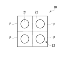
- FIG. 2 is a plan view that typically illustrates the planar configuration of the photoelectric conversion layer shown in FIG.
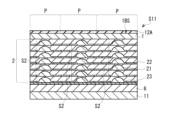
- FIG. 3A is a cross-sectional view that typically illustrates one step of a method for manufacturing the photodetector element shown in FIG.
- FIG. 3B is a cross-sectional view that diagrammatically illustrates a step subsequent to FIG. 3A.
- FIG. 3C is a cross-sectional view that diagrammatically illustrates a step subsequent to FIG. 3B.
- FIG. 3D is a cross-sectional view that diagrammatically illustrates a step subsequent to FIG. 3C.
- FIG. 3E is a cross-sectional view that diagrammatically illustrates a step subsequent to FIG. 3D.
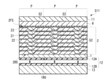
- FIG. 3F is a cross-sectional view that diagrammatically illustrates a step subsequent to FIG. 3E.
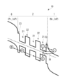
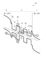
- FIG. 4A is a schematic diagram showing the potential in the photodetector element shown in FIG. 1 and the behavior when infrared light is incident thereon.
- FIG. 4B is a schematic diagram showing the potential in the photodetector element shown in FIG. 1 and the behavior when infrared light is incident thereon.
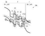
- FIG. 5A is a cross-sectional view illustrating a schematic configuration of a light detection element according to a first modified example of the present disclosure.
- FIG. 5B is a schematic diagram showing the potential in the photodetector element shown in FIG.
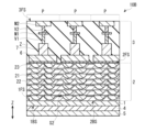
- FIG. 6A is a cross-sectional view illustrating a schematic configuration of a light detection element according to a second modification of the present disclosure.
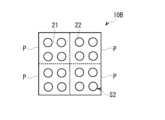
- FIG. 6B is a plan view that typically illustrates the planar configuration of the photoelectric conversion layer illustrated in FIG. 6A.
- FIG. 7 is a cross-sectional view illustrating a schematic configuration of a light detection element according to a third modified example of the present disclosure.
- FIG. 8A is a cross-sectional view illustrating a schematic configuration of a photodetector according to a fourth modified example of the present disclosure.
- FIG. 8B is a schematic diagram showing the potential in the photodetector element shown in FIG.
- FIG. 9 is a diagram showing a schematic configuration of an image sensor having the photodetector element shown in FIG.
- FIG. 10 is a diagram showing a schematic configuration of an electronic device to which the image sensor shown in FIG. 9 is applied.
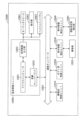
- FIG. 11 is a block diagram showing a schematic configuration example of a vehicle control system.
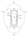
- FIG. 12 is an explanatory diagram showing an example of the installation position of the imaging unit.
- FIG. 10 is a cross-sectional view that typically illustrates an example of a cross-sectional configuration of a photodetection element 10 according to an embodiment of the present disclosure.
- the photodetection element 10 is an element that can detect incident light.
- the photodetection element 10 has a plurality of pixels P each having a photoelectric conversion layer 2, and is configured to perform photoelectric conversion of the incident light for each pixel P to generate a signal.
- the photodetection element 10 can be applied to an image sensor, a distance measurement sensor, and the like.
- the photodetector element 10 has a laminated structure in which a first conductive type semiconductor layer 1, a photoelectric conversion layer 2, and a multilayer wiring layer 3 are laminated in this order.
- the stacking direction of this laminated structure is defined as the Z direction.
- the photoelectric conversion layer 2 is provided on the front surface 1FS of the first conductive type semiconductor layer 1.
- a transparent electrode layer 4 and a protective film 5 are provided in this order on the back surface 1BS of the first conductive type semiconductor layer 1.
- light irradiated to the protective film 5 passes through the transparent electrode layer 4 and the first conductive type semiconductor layer 1 in this order and enters the photoelectric conversion layer 2.
- the first conductive type semiconductor layer 1 is provided on the light incident side of the photoelectric conversion layer 2.
- the first conductive type semiconductor layer 1 is provided, for example, in common to all pixels P.
- the first conductive type semiconductor layer 1 is provided between the photoelectric conversion layer 2 and the transparent electrode layer 4.
- the front surface 1FS of the first conductive type semiconductor layer 1 is in contact with the photoelectric conversion layer 2, and the back surface 1BS of the first conductive type semiconductor layer 1 is in contact with the transparent electrode layer 4.
- the first conductive type semiconductor layer 1 is a region where charges discharged from the transparent electrode layer 4 move, and is composed of, for example, a compound semiconductor containing n-type impurities.
- n-type InP indium phosphide
- Another layer may be interposed between the first conductive type semiconductor layer 1 and the photoelectric conversion layer 2.
- materials for the layer interposed between the first conductive type semiconductor layer 1 and the photoelectric conversion layer 2 include semiconductor materials such as InAlAs, Ge, Si, GaAs, and InP, but it is preferable to select a material that is lattice-matched between the first conductive type semiconductor layer 1 and the photoelectric conversion layer 2.
- the photoelectric conversion layer 2 absorbs light of a predetermined wavelength (for example, light of a wavelength in the infrared region) and generates electric charges (electrons or holes).
- the photoelectric conversion layer 2 has a stack S2 having a semiconductor quantum dot layer 21 and a semiconductor spacer layer 22.
- the semiconductor quantum dot layer 21 and the semiconductor spacer layer 22 are alternately stacked multiple times in the Z direction.
- a plurality of stacks S2 are provided in the commonly provided photoelectric conversion layer 2.
- each of the multiple pixels P includes one stack S2.
- the semiconductor quantum dot layer 21 includes a thick portion 21A and a thin portion 21B that is thinner than the thick portion 21A.
- the thick portion 21A is provided discretely for each pixel P.
- the thin portion 21B extends along a plane perpendicular to the Z direction and is provided in common to a plurality of pixels P.
- the stack S2 is formed by repeatedly stacking the thick portion 21A of the semiconductor quantum dot layer 21, which is thicker than the thin portion 21B, and the semiconductor spacer layer 22 in the Z direction. As shown in FIG. 2, the plurality of stacks S2 are separated from each other in an in-plane direction perpendicular to the Z direction.
- the plurality of thick portions 21A are embedded in one semiconductor spacer layer 22 provided in common to a plurality of pixels P.
- the semiconductor quantum dot layer 21 of the top layer of each stack S2 is exposed on the surface 2FS of the photoelectric conversion layer 2.
- the semiconductor quantum dot layer 21 contains a plurality of quantum dots of a first semiconductor having a first band gap. Each of the quantum dots is made of a three-dimensionally minute semiconductor (having a diameter of about a few nm) and has the property of easily capturing electric charges.
- the semiconductor spacer layer 22 contains a second semiconductor having a second band gap larger than the first band gap of the first semiconductor.
- the first semiconductor quantum dots constituting the semiconductor quantum dot layer 21 can be a compound semiconductor that absorbs infrared rays, such as InAs.
- the second semiconductor constituting the semiconductor spacer layer 22 can be InP or GaAs.
- the semiconductor spacer layer 22 has a thickness that allows tunneling of charges in the Z direction.
- the semiconductor spacer layer 22 has a thickness of, for example, 1 nm or more and 3 nm or less at its thinnest portion.
- the second semiconductor constituting the semiconductor spacer layer 22 preferably has the same lattice constant as the first semiconductor constituting the semiconductor quantum dot layer 21 and the lattice constant of the first conductivity type semiconductor constituting the first conductivity type semiconductor layer 1.
- the second semiconductor constituting the semiconductor spacer layer 22 preferably has the same lattice constant as the first semiconductor constituting the semiconductor quantum dot layer 21 and the lattice constant of the second conductivity type semiconductor layer 6 described below.
- the multi-layer wiring layer 3 has a second conductive type semiconductor layer 6, a counter electrode 7, vias V1 and V2, and wiring layers M1 and M2.
- each of the multiple pixels P has a stack S3 of the second conductive type semiconductor layer 6, the counter electrode 7, the via V1, the wiring layer M1, the via V2, and the wiring layer M2, which are stacked in order from the photoelectric conversion layer 2 side.
- the multiple stacks S3 are embedded in the insulating layer Z.
- the insulating film Z is made of, for example, an inorganic insulating material.
- Each of the multiple stacks S3 further includes a semiconductor spacer layer 23 between the second conductive type semiconductor layer 6 and the semiconductor quantum dot layer 21, which is the uppermost layer of the photoelectric conversion layer 2.
- the semiconductor spacer layer 23 can be made of, for example, the second semiconductor that constitutes the semiconductor spacer layer 22.
- the semiconductor spacer layer 23 has a thickness that allows tunneling of charges in the Z direction.
- the semiconductor spacer layer 23 has a thickness of, for example, 1 nm or more and 3 nm or less at its thinnest portion.
- a first conductive type semiconductor layer 1 is provided with a plurality of second conductive type semiconductor layers 6 that are separated from each other.
- a plurality of counter electrodes 7 are provided corresponding to the plurality of second conductive type semiconductor layers 6, and each of the plurality of counter electrodes 7 and each of the plurality of second conductive type semiconductor layers 6 are electrically connected to each other.
- the second conductive type semiconductor layer 6, the counter electrode 7, the via V1, the wiring layer M1, the via V2, and the wiring layer M2 are electrically connected to each other.
- the wiring layer M2 is exposed on the surface 3FS of the multi-layer wiring layer 3, and serves as a connection terminal to the outside.
- the vias V1, V2 and the wiring layers M1, M2 can be made of a highly conductive material such as Cu (copper).
- the second conductive type semiconductor layers 6 are provided at a distance from each other for each pixel P.
- the second conductive type semiconductor layers 6 are regions where charges generated in the photoelectric conversion layer 2 move, and are, for example, regions containing p-type impurities (p-type impurity regions).
- p-type impurities p-type impurity regions.
- p-type InP indium phosphide
- the band gap of the first conductive type semiconductor constituting the first conductive type semiconductor layer 1 and the band gap of the second conductive type semiconductor constituting the second conductive type semiconductor layer 6 are both preferably larger than the first band gap of the first semiconductor constituting the quantum dots of the semiconductor quantum dot layer 21.
- the counter electrode 7 as the second electrode is a readout electrode to which a voltage is supplied for reading out the electric charge (holes or electrons) generated in the photoelectric conversion layer 2.
- the counter electrode 7 is provided for each pixel P so as to face the surface 2FS of the photoelectric conversion layer 2 across the second conductive type semiconductor layer 6. That is, the counter electrode 7 is located on the opposite side of the photoelectric conversion layer 2 as viewed from the second conductive type semiconductor layer 6.
- the counter electrode 7 is connected to a pixel circuit for signal readout, for example, via vias V1, V2 and wiring layers M1, M2.
- the counter electrode 7 is connected to the semiconductor quantum dot layer 21 exposed on the surface 2FS through a semiconductor spacer layer 22.
- the planar shape of the counter electrode 7 is, for example, a square shape.
- An insulating layer Z is filled between adjacent counter electrodes 7.
- the counter electrode 7 is composed of, for example, any one of Ti (titanium), W (tungsten), TiN (titanium nitride), Pt (platinum), Au (gold), Cu (copper), Ge (germanium), Pd (palladium), Zn (zinc), Ni (nickel), In (indium) and Al (aluminum), or an alloy containing at least one of them.
- the counter electrode 7 may be a single film of such a constituent material, or may be a laminated film consisting of two or more layers.
- the transparent electrode layer 4 as the first electrode is provided, for example, as an electrode common to each pixel P, so as to cover the entire back surface 2BS (light incident surface) of the photoelectric conversion layer 2 via the first conductive type semiconductor layer 1.
- the transparent electrode layer 4 is for discharging charges that are not used as signal charges among the charges generated in the photoelectric conversion layer 2. For example, when electrons are read out as signal charges from the counter electrode 7, for example, holes can be discharged through the transparent electrode layer 4.
- the transparent electrode layer 4 is made of a transparent conductive film that can transmit incident light such as infrared rays, and has a transmittance of 50% or more for light with a wavelength of 1.6 ⁇ m (1600 nm).
- ITO Indium Tin Oxide
- ITiO In 2 O 3 -TiO 2
- the protective film 5 is a passivation film that physically and chemically protects the transparent electrode layer 4, the first conductive type semiconductor layer 1, the photoelectric conversion layer 2, etc.
- the protective film 5 is made of a transparent resin that can transmit incident light such as infrared rays.
- the light detection element 10 can be manufactured, for example, as follows: Figures 3A to 3F show the manufacturing process of the light detection element 10 in order of steps.
- a compound semiconductor stack S11 is formed. Specifically, for example, a semiconductor substrate 11 made of InP is prepared, and then a second conductive type semiconductor layer 6 made of, for example, p-type InP is formed on the semiconductor substrate 11. Next, a semiconductor spacer layer 23 is formed so as to cover the second conductive type semiconductor layer 6. Furthermore, a semiconductor quantum dot layer 21 made of InAs and a semiconductor spacer layer 22 made of InP or GaAs are alternately stacked to obtain a photoelectric conversion layer 2. Then, a first conductive type semiconductor layer 1 made of n-type InP is stacked so as to cover the photoelectric conversion layer 2, thereby obtaining a stack S11.
- the stack S11 can be formed by an epitaxy method such as MBE (Molecular Beam Epitaxy) and migration enhanced epitaxy (MEE).
- the laminate S11 may be formed by a method such as MOCVD (Metal Organic Chemical Vapor Deposition), hydride vapor phase epitaxy (HVPE) in which halogens contribute to transport or reaction, ALD (Atomic Layer Deposition), or plasma-assisted physical vapor phase deposition (PPD).
- MOCVD Metal Organic Chemical Vapor Deposition
- HVPE hydride vapor phase epitaxy
- ALD Atomic Layer Deposition
- PPD plasma-assisted physical vapor phase deposition
- an adhesive layer 12A is applied to the back surface 1BS of the first conductive type semiconductor layer 1.
- the laminate S11 shown in FIG. 3A is turned upside down and adhered to a silicon substrate 13 via an adhesive layer 12.
- an adhesive layer 12B is formed on the surface of the silicon substrate 13, and then adhesive layers 12A and 12B are placed opposite each other and bonded to each other to form an integral adhesive layer 12.
- the semiconductor substrate 11 is entirely removed from the laminate S11 by etching, and the second conductive type semiconductor layer 6 and the semiconductor spacer layer 23 are selectively removed to form a plurality of laminates of the semiconductor spacer layer 23 and the second conductive type semiconductor layer 6 as shown in FIG. 3C.
- one laminate of the semiconductor spacer layer 23 and the second conductive type semiconductor layer 6 is formed for each region that becomes one pixel P.
- a counter electrode 7 is formed on each of the second conductive type semiconductor layers 6.
- vias V1, wiring layers M1, vias V2, and wiring layers M2 embedded in insulating layer Z are formed on the multiple opposing electrodes 7.
- a circuit board including a readout circuit may be separately attached.
- the silicon substrate 13 is peeled off from the laminate S11, and the adhesive layer 12 is removed to expose the back surface 1BS of the first conductivity type semiconductor layer 1.
- the transparent electrode layer 4 and the protective film 5 are sequentially laminated to cover the back surface 1BS. This completes the photodetector element 10 shown in FIG. 1.
- the photodetection element 10 In the photodetector element 10, light (e.g., light with a wavelength in the infrared region) is incident on the photoelectric conversion layer 2 through the protective film 5 and the transparent electrode layer 4, and the light incident on the photoelectric conversion layer 2 is absorbed in the photoelectric conversion layer 2. As a result, pairs of holes and electrons are generated in the photoelectric conversion layer 2, i.e., photoelectric conversion occurs. At this time, for example, when a predetermined voltage is applied to the counter electrode 7, a potential gradient is generated in the photoelectric conversion layer 2, and one of the generated charges moves to the second conductivity type semiconductor layer 6 as a signal charge and is then collected from the second conductivity type semiconductor layer 6 to the counter electrode 7. This signal charge is read out by a readout circuit in the multilayer wiring layer 3.
- a predetermined voltage is applied to the counter electrode 7
- a potential gradient is generated in the photoelectric conversion layer 2
- one of the generated charges moves to the second conductivity type semiconductor layer 6 as a signal charge and is then
- a photoelectric conversion layer 2 including a laminate S2 having a semiconductor quantum dot layer 21 and a semiconductor spacer layer 22 is sandwiched between a first conductivity type semiconductor layer 1 and a second conductivity type semiconductor layer 6. For this reason, charges generated by light transmitted through the first conductivity type semiconductor layer 1 and incident on the semiconductor quantum dot layer 21 can easily reach the second conductivity type semiconductor layer 6 through the semiconductor spacer layer 22.
- FIG. 4A and 4B are schematic diagrams showing the potential in the photodetector element 10 shown in FIG. 1.
- FIG. 4A shows the behavior of the charge when infrared light is incident on the photoelectric conversion layer 2
- FIG. 4B shows the behavior of the charge when visible light is incident on the photoelectric conversion layer 2.
- FIG. 4A when infrared light is incident on the photoelectric conversion layer 2, charges (holes and electrons) are generated in the semiconductor quantum dot layer 21.
- the generated holes and electrons tunnel through the semiconductor spacer layer 22, which has a higher potential than the potential of the semiconductor quantum dot layer 21, and the holes reach, for example, the second conductive type semiconductor layer 6, and the electrons reach the first conductive type semiconductor layer 1.
- FIG. 4A shows the behavior of the charge when infrared light is incident on the photoelectric conversion layer 2
- FIG. 4B shows the behavior of the charge when visible light is incident on the photoelectric conversion layer 2.
- FIG. 4A when infrared light is incident on the photoelectric conversion layer 2, charges
- tunneling is more likely to occur when the thinnest part of the semiconductor spacer layer 22 has a thickness of 1 nm or more and 3 nm or less.
- the lattice constant of the first semiconductor constituting the semiconductor quantum dot layer 21 is slightly different from the lattice constant of the second semiconductor constituting the semiconductor spacer layer 22, so that the tiny quantum dots in the semiconductor quantum dot layer 21 are well formed by self-formation of the SK mode.
- the light detection element 10 leakage of electric charge to adjacent pixels P can be prevented without providing an isolation structure such as a partition between multiple pixels P, so the photoelectric conversion layer 2 can be provided without gaps. Therefore, the light receiving sensitivity can be increased compared to the case where an isolation structure is provided between the pixels as described above.
- ⁇ Modification 1> 5A is a cross-sectional view that shows a schematic configuration of a photodetector 10A according to a first modified example of the present disclosure.
- a p-type impurity diffusion layer 6A is provided instead of the second conductive type semiconductor layer 6.
- the impurity diffusion layer 6A is in contact with the semiconductor quantum dot layer 21 located in the uppermost layer of the stack S2 of the photoelectric conversion layer 2.
- the configuration of the photodetector 10A is substantially the same as the configuration of the photodetector 10.
- the photodetector 10A of this modified example is expected to have the same effect as the photodetector 10 of the above embodiment.
- the impurity diffusion layer 6A as the second conductive type semiconductor layer is in direct contact with the semiconductor quantum dot layer 21, so that as shown in FIG. 5B, the barrier from the semiconductor quantum dot layer 21 to the counter electrode 7 is lower than that of the photodetector 10, and charges (e.g., holes) can easily reach the counter electrode 7 from the semiconductor quantum dot layer 21. This further improves the sensitivity.
- FIG. 5B is a schematic diagram showing the potential in the photodetector 10A shown in FIG. 5A and the behavior when infrared light and visible light are incident.
- FIG. 6A is a cross-sectional view that shows a schematic configuration of a photodetector 10B according to a second modified example of the present disclosure.
- FIG. 6B is a plan view that shows a schematic planar configuration of a photoelectric conversion layer 2B in the photodetector 10B.
- a plurality of stacked bodies S2 are provided for each of a plurality of second conductive type semiconductor layers 6.
- the configuration of the photodetector 10B is substantially the same as the configuration of the photodetector 10, except for the above points. Note that FIG. 6A and FIG.
- FIG. 6B show an example in which four stacked bodies S2 arranged in two rows and two columns are provided for one pixel P, but the present disclosure is not limited thereto. Two, three, or five or more stacked bodies S2 may be arranged for one pixel P. The layout of the stacked bodies S2 can be selected arbitrarily.
- the photodetection element 10B of this modified example is expected to have the same effect as the photodetection element 10 of the above embodiment.
- multiple stacked bodies S2 are provided in the photoelectric conversion layer 2 corresponding to one pixel P, which improves the probability that the quantum dots will capture the charge generated in the photoelectric conversion layer 2. This makes it possible to more effectively prevent the occurrence of crosstalk and achieve better photodetection performance.
- ⁇ Modification 3> 7 is a cross-sectional view showing a schematic configuration of a photodetector 10C according to a third modified example of the present disclosure.
- a part of the semiconductor spacer layers 22 constituting the stack S2 of the photoelectric conversion layer 2 is replaced with a strain relaxation layer 8.
- the configuration of the photodetector 10C is substantially the same as that of the photodetector 10, except for the above points.
- a constituent material of the strain relaxation layer 8 a semiconductor having a lattice constant between the lattice constant of the first semiconductor of the semiconductor quantum dot layer 21 and the lattice constant of the second semiconductor of the semiconductor spacer layer 22 is used.
- the quantum dots of the first semiconductor of the semiconductor quantum dot layer 21 are InAs and the second semiconductor of the semiconductor spacer layer 22 are GaAs
- InGaAs can be used.
- a semiconductor such as InGaAs having an indium composition of greater than 53% can be used.
- the photodetector element 10C of this modified example is expected to have the same effect as the photodetector element 10 of the above embodiment.
- a strain relaxation layer 8 is inserted in the photoelectric conversion layer 2, which improves the crystallinity of the photoelectric conversion layer 2 and further improves the readout characteristics, such as suppressing the generation of dark current.
- FIG. 8A is a cross-sectional view that shows a schematic configuration of a photodetector 10D according to a fourth modified example of the present disclosure.
- FIG. 8B is a schematic diagram showing the potential in the photodetector 10D shown in FIG. 8A and the behavior when infrared light and visible light are incident.
- a barrier layer 9 is further added between the second conductive type semiconductor layer 6 and the photoelectric conversion layer 2. Except for the above points, the configuration of the photodetector 10D is substantially the same as the configuration of the photodetector 10.
- the barrier layer 9 disposed between the first conductive type semiconductor layer 1 and the second conductive type semiconductor layer 6 is a semiconductor layer that prevents the passage of either holes or electrons. That is, the barrier layer 9 is a layer that serves as a barrier only against charges of the opposite sign to the charge to be read.
- the barrier layer 9 can be made of a semiconductor material whose bottom of the conduction band is sufficiently higher than the potential of the semiconductor spacer layer 22 and the potential of the semiconductor quantum dot layer 21, and whose top of the valence band is equivalent to the potential of the semiconductor quantum dot layer 21.
- the barrier layer 9 can be made of a semiconductor material whose top of the valence band is sufficiently lower than the potential of the semiconductor quantum dot layer 21 and the potential of the semiconductor spacer layer 22, and whose bottom of the conduction band is equivalent to the potential of the semiconductor quantum dot layer 21.
- the first semiconductor of the semiconductor quantum dot layer 21 is InAs and the second semiconductor of the semiconductor spacer layer 22 is GaAs
- p-type AlGaAs can be used as the semiconductor constituting the barrier layer 9.
- the photodetection element 10D of this modified example is expected to have the same effect as the photodetection element 10 of the above embodiment.
- the photodetection element 10D has a barrier layer 9, which can suppress recombination of electrons and holes generated in the photoelectric conversion layer 2. Therefore, the photodetection sensitivity of the photodetection element 10D is improved compared to the photodetection element 10.
- Application Example 1> 9 shows the functional configuration of an image sensor 100 using the photodetection element 10 (or the photodetection elements 10A-10D of Modifications 1-4) described in the above embodiment and the like.
- the image sensor 100 is, for example, an infrared image sensor, and has, for example, a pixel section 1a on a substrate 20, and a peripheral circuit section 230 that drives the pixel section 1a.
- the peripheral circuit section 230 has, for example, a row scanning section 231, a horizontal selection section 233, a column scanning section 234, and a system control section 232.
- the pixel section 1a has a number of pixels P arranged two-dimensionally, for example, in a matrix.
- a pixel drive line Lread (for example, a row selection line and a reset control line) is wired, for example, for each pixel row, and a vertical signal line Lsig is wired for each pixel column.
- the pixel drive line Lread transmits a drive signal for reading out a signal from the pixel P.
- One end of the pixel drive line Lread is connected to an output terminal of the row scanning section 231 corresponding to each row.
- the row scanning unit 231 is a pixel driving unit that is composed of a shift register, an address decoder, etc., and drives each pixel P of the pixel unit 1a, for example, on a row-by-row basis.
- the signals output from each pixel P of the pixel row selected and scanned by the row scanning unit 231 are supplied to the horizontal selection unit 233 through each of the vertical signal lines Lsig.
- the horizontal selection unit 233 is composed of an amplifier, a horizontal selection switch, etc., provided for each vertical signal line Lsig.
- the column scanning unit 234 is composed of a shift register, an address decoder, etc., and drives each horizontal selection switch of the horizontal selection unit 233 in sequence while scanning them. Through selective scanning by this column scanning unit 234, the signals of each pixel transmitted through each of the vertical signal lines Lsig are output in sequence to the horizontal signal line 235, and input to a signal processing unit (not shown) through the horizontal signal line 235.
- the system control unit 232 receives an externally provided clock, data instructing the operating mode, and the like, and also outputs data such as internal information of the image sensor 100.
- the system control unit 232 further has a timing generator that generates various timing signals, and performs drive control of the row scanning unit 231, horizontal selection unit 233, column scanning unit 234, and the like based on the various timing signals generated by the timing generator.
- the above-mentioned imaging element 100 can be applied to various types of electronic devices, such as a camera capable of capturing images in the infrared region.
- Fig. 10 shows a schematic configuration of an electronic device 102 (camera) as an example.
- the electronic device 102 is, for example, a camera capable of capturing still images or videos, and includes the imaging element 100, an optical system (optical lens) 310, a shutter device 311, a drive unit 313 that drives the imaging element 100 and the shutter device 311, and a signal processing unit 312.
- the optical system 310 guides image light (incident light) from a subject to the image sensor 100.
- This optical system 310 may be composed of multiple optical lenses.
- the shutter device 311 controls the light irradiation period and light blocking period to the image sensor 100.
- the drive unit 313 controls the transfer operation of the image sensor 100 and the shutter operation of the shutter device 311.
- the signal processing unit 312 performs various signal processing on the signal output from the image sensor 100.
- the video signal Dout after signal processing is stored in a storage medium such as a memory, or is output to a monitor, etc.
- the light detection element 10 (or light detection elements 10A to 10D) described in the present embodiment can also be applied to the following electronic devices (capsule endoscope 10100 and moving objects such as vehicles):
- the technology according to the present disclosure can be applied to various products.
- the technology according to the present disclosure may be realized as a device mounted on any type of moving body such as an automobile, an electric vehicle, a hybrid electric vehicle, a motorcycle, a bicycle, a personal mobility device, an airplane, a drone, a ship, or a robot.
- FIG. 11 is a block diagram showing a schematic configuration example of a vehicle control system, which is an example of a mobile object control system to which the technology disclosed herein can be applied.
- the vehicle control system 12000 includes a plurality of electronic control units connected via a communication network 12001.
- the vehicle control system 12000 includes a drive system control unit 12010, a body system control unit 12020, an outside vehicle information detection unit 12030, an inside vehicle information detection unit 12040, and an integrated control unit 12050.
- Also shown as functional components of the integrated control unit 12050 are a microcomputer 12051, an audio/video output unit 12052, and an in-vehicle network I/F (interface) 12053.
- the drive system control unit 12010 controls the operation of devices related to the drive system of the vehicle according to various programs.
- the drive system control unit 12010 functions as a control device for a drive force generating device for generating the drive force of the vehicle, such as an internal combustion engine or a drive motor, a drive force transmission mechanism for transmitting the drive force to the wheels, a steering mechanism for adjusting the steering angle of the vehicle, and a braking device for generating a braking force for the vehicle.
- the body system control unit 12020 controls the operation of various devices installed in the vehicle body according to various programs.
- the body system control unit 12020 functions as a control device for a keyless entry system, a smart key system, a power window device, or various lamps such as headlamps, tail lamps, brake lamps, turn signals, and fog lamps.
- radio waves or signals from various switches transmitted from a portable device that replaces a key can be input to the body system control unit 12020.
- the body system control unit 12020 accepts the input of these radio waves or signals and controls the vehicle's door lock device, power window device, lamps, etc.
- the outside-vehicle information detection unit 12030 detects information outside the vehicle equipped with the vehicle control system 12000.
- the image capturing unit 12031 is connected to the outside-vehicle information detection unit 12030.
- the outside-vehicle information detection unit 12030 causes the image capturing unit 12031 to capture images outside the vehicle and receives the captured images.
- the outside-vehicle information detection unit 12030 may perform object detection processing or distance detection processing for people, cars, obstacles, signs, characters on the road surface, etc. based on the received images.
- the imaging unit 12031 is an optical sensor that receives light and outputs an electrical signal according to the amount of light received.
- the imaging unit 12031 can output the electrical signal as an image, or as distance measurement information.
- the light received by the imaging unit 12031 may be visible light, or may be invisible light such as infrared light.
- the in-vehicle information detection unit 12040 detects information inside the vehicle.
- a driver state detection unit 12041 that detects the state of the driver is connected.
- the driver state detection unit 12041 includes, for example, a camera that captures an image of the driver, and the in-vehicle information detection unit 12040 may calculate the driver's degree of fatigue or concentration based on the detection information input from the driver state detection unit 12041, or may determine whether the driver is dozing off.
- the microcomputer 12051 can calculate control target values for the driving force generating device, steering mechanism, or braking device based on information inside and outside the vehicle acquired by the outside vehicle information detection unit 12030 or the inside vehicle information detection unit 12040, and output control commands to the drive system control unit 12010.
- the microcomputer 12051 can perform cooperative control aimed at realizing the functions of an ADAS (Advanced Driver Assistance System), including vehicle collision avoidance or impact mitigation, following driving based on the distance between vehicles, maintaining vehicle speed, vehicle collision warning, or vehicle lane departure warning.
- ADAS Advanced Driver Assistance System
- the microcomputer 12051 can also perform cooperative control for the purpose of autonomous driving, which allows the vehicle to travel autonomously without relying on the driver's operation, by controlling the driving force generating device, steering mechanism, braking device, etc. based on information about the surroundings of the vehicle acquired by the outside vehicle information detection unit 12030 or the inside vehicle information detection unit 12040.
- the microcomputer 12051 can also output control commands to the body system control unit 12020 based on information outside the vehicle acquired by the outside information detection unit 12030. For example, the microcomputer 12051 can control the headlamps according to the position of a preceding vehicle or an oncoming vehicle detected by the outside information detection unit 12030, and perform cooperative control aimed at preventing glare, such as switching from high beams to low beams.
- the audio/image output unit 12052 transmits at least one output signal of audio and image to an output device capable of visually or audibly notifying the occupants of the vehicle or the outside of the vehicle of information.
- an audio speaker 12061, a display unit 12062, and an instrument panel 12063 are exemplified as output devices.
- the display unit 12062 may include, for example, at least one of an on-board display and a head-up display.
- FIG. 12 shows an example of the installation position of the imaging unit 12031.
- the imaging unit 12031 includes imaging units 12101, 12102, 12103, 12104, and 12105.
- the imaging units 12101, 12102, 12103, 12104, and 12105 are provided, for example, at the front nose, side mirrors, rear bumper, back door, and upper part of the windshield inside the vehicle cabin of the vehicle 12100.
- the imaging unit 12101 provided at the front nose and the imaging unit 12105 provided at the upper part of the windshield inside the vehicle cabin mainly acquire images of the front of the vehicle 12100.
- the imaging units 12102 and 12103 provided at the side mirrors mainly acquire images of the sides of the vehicle 12100.
- the imaging unit 12104 provided at the rear bumper or back door mainly acquires images of the rear of the vehicle 12100.
- the imaging unit 12105 provided at the upper part of the windshield inside the vehicle cabin is mainly used to detect leading vehicles, pedestrians, obstacles, traffic lights, traffic signs, lanes, etc.
- FIG. 12 shows an example of the imaging ranges of the imaging units 12101 to 12104.
- Imaging range 12111 indicates the imaging range of the imaging unit 12101 provided on the front nose
- imaging ranges 12112 and 12113 indicate the imaging ranges of the imaging units 12102 and 12103 provided on the side mirrors, respectively
- imaging range 12114 indicates the imaging range of the imaging unit 12104 provided on the rear bumper or back door.
- an overhead image of the vehicle 12100 viewed from above is obtained by superimposing the image data captured by the imaging units 12101 to 12104.
- At least one of the imaging units 12101 to 12104 may have a function of acquiring distance information.
- at least one of the imaging units 12101 to 12104 may be a stereo camera consisting of multiple imaging elements, or an imaging element having pixels for phase difference detection.
- the microcomputer 12051 can obtain the distance to each solid object within the imaging ranges 12111 to 12114 and the change in this distance over time (relative speed with respect to the vehicle 12100) based on the distance information obtained from the imaging units 12101 to 12104, and can extract as a preceding vehicle, in particular, the closest solid object on the path of the vehicle 12100 that is traveling in approximately the same direction as the vehicle 12100 at a predetermined speed (e.g., 0 km/h or faster). Furthermore, the microcomputer 12051 can set the inter-vehicle distance that should be maintained in advance in front of the preceding vehicle, and perform automatic braking control (including follow-up stop control) and automatic acceleration control (including follow-up start control). In this way, cooperative control can be performed for the purpose of automatic driving, which runs autonomously without relying on the driver's operation.
- automatic braking control including follow-up stop control
- automatic acceleration control including follow-up start control
- the microcomputer 12051 classifies and extracts three-dimensional object data on three-dimensional objects, such as two-wheeled vehicles, ordinary vehicles, large vehicles, pedestrians, utility poles, and other three-dimensional objects, based on the distance information obtained from the imaging units 12101 to 12104, and can use the data to automatically avoid obstacles.
- the microcomputer 12051 distinguishes obstacles around the vehicle 12100 into obstacles that are visible to the driver of the vehicle 12100 and obstacles that are difficult to see.
- the microcomputer 12051 determines the collision risk, which indicates the risk of collision with each obstacle, and when the collision risk is equal to or exceeds a set value and there is a possibility of a collision, it can provide driving assistance for collision avoidance by outputting an alarm to the driver via the audio speaker 12061 or the display unit 12062, or by performing forced deceleration or avoidance steering via the drive system control unit 12010.
- At least one of the imaging units 12101 to 12104 may be an infrared camera that detects infrared rays.
- the microcomputer 12051 can recognize a pedestrian by determining whether or not a pedestrian is present in the image captured by the imaging units 12101 to 12104. The recognition of such a pedestrian is performed, for example, by a procedure of extracting feature points in the image captured by the imaging units 12101 to 12104 as infrared cameras, and a procedure of performing pattern matching processing on a series of feature points that indicate the contour of an object to determine whether or not it is a pedestrian.
- the audio/image output unit 12052 controls the display unit 12062 to superimpose a rectangular contour line for emphasis on the recognized pedestrian.
- the audio/image output unit 12052 may also control the display unit 12062 to display an icon or the like indicating a pedestrian at a desired position.
- the technology of the present disclosure can be applied to, for example, the imaging unit 12031 among the configurations described above.
- the technology of the present disclosure By applying the technology of the present disclosure to the imaging unit 12031, it is possible to obtain a captured image that is easier to see, thereby reducing driver fatigue.
- the present technology has been described above with reference to embodiments and modified examples, but the present technology is not limited to the above-mentioned embodiments, etc., and various modifications are possible.
- the layer configuration of the light detection element described in the above-mentioned embodiments, etc. is one example, and the light detection element may further include other layers.
- the materials and thicknesses of each layer are also one example, and are not limited to those described above.
- a photoelectric conversion layer including a laminate having a semiconductor quantum dot layer and a semiconductor spacer layer is sandwiched between a first conductive type semiconductor layer and a second conductive type semiconductor layer. Therefore, charges generated by light transmitted through the first conductive type semiconductor layer being incident on the semiconductor quantum dot layer move along the stacking direction of the semiconductor quantum dot layer and the semiconductor spacer layer. Therefore, the charge generated in the photoelectric conversion layer of a pixel is prevented from leaking to other pixels adjacent to that pixel. This makes it possible to prevent crosstalk from occurring and to exhibit good photodetection performance.
- a first electrode a first conductive type semiconductor layer provided on the first electrode and made of a first conductive type semiconductor; a second conductive type semiconductor layer made of a second conductive type semiconductor; a photoelectric conversion layer sandwiched between the first conductive type semiconductor layer and the second conductive type semiconductor layer; a second electrode located on the opposite side of the photoelectric conversion layer from the second conductive type semiconductor layer and connected to the second conductive type semiconductor layer;
- the photoelectric conversion layer is a laminate including a semiconductor quantum dot layer including quantum dots of a first semiconductor having a first band gap, and a semiconductor spacer layer including a second semiconductor having a second band gap larger than the first band gap.
- a plurality of the second conductive type semiconductor layers separated from each other are provided for one of the first conductive type semiconductor layers, A plurality of the second electrodes are provided corresponding to the plurality of second conductive type semiconductor layers, The light-detecting element according to ⁇ 1> above, wherein each of the plurality of second electrodes and each of the plurality of second conductive type semiconductor layers are electrically connected to each other.
- the photoelectric conversion layer includes a plurality of the stacked bodies separated from each other in an in-plane direction perpendicular to a stacking direction of the semiconductor quantum dot layer and the semiconductor spacer layer,
- the second semiconductor of the semiconductor spacer layer has a lattice constant that is the same as the lattice constant of the first semiconductor of the semiconductor quantum dot layer, and a lattice constant of both the first conductivity type semiconductor and the lattice constant of the second conductivity type semiconductor.
- ⁇ 7> The photodetector according to any one of ⁇ 1> to ⁇ 6>, wherein the second conductive type semiconductor layer is a diffusion layer in contact with the semiconductor quantum dot layer.
- the photoelectric conversion layer further includes an additional semiconductor layer made of a third semiconductor having a lattice constant between the lattice constants of the first semiconductor and the lattice constants of the second semiconductor.
- the photodetector element according to claim 1 wherein the first semiconductor is a compound semiconductor that absorbs infrared rays.
- the photoelectric conversion layer is a laminate including a semiconductor quantum dot layer including quantum dots of a first semiconductor having a first band gap, and a semiconductor spacer layer including a second semiconductor having a second band gap larger than the first band gap.
Landscapes
- Light Receiving Elements (AREA)
Abstract
良好な光検出性能を有する光検出素子(10)を提供する。本開示の一実施形態の光検出素子(10)は、第1導電型半導体からなる第1導電型半導体層(1)と、第2導電型半導体からなる第2導電型半導体層(6)と、それら第1導電型半導体層(1)と第2導電型半導体層(6)との間に挟まれた光電変換層(2)と、第2導電型半導体層(6)から見て光電変換層(2)の反対側に位置すると共に第2導電型半導体層(6)と接続された電極層(7)とを有する。ここで光電変換層(2)は、第1のバンドギャップを有する第1半導体の量子ドットを含む半導体量子ドット層(21)と、第1のバンドギャップよりも大きな第2のバンドギャップを有する第2半導体を含む半導体スペーサ層(22)とを有する積層体(S2)である。
Description
本開示は、光検出素子および撮像素子に関する。
隣り合う画素の間に拡散領域を設けることで画素分離を行うようにした撮像素子が提案されている(特許文献1)。
光検出素子では、光検出性能を向上させることが望ましい。
よって、良好な光検出性能を有する光検出素子を提供することが望まれる。
本開示の一実施形態の光検出素子は、第1導電型半導体からなる第1導電型半導体層と、第2導電型半導体からなる第2導電型半導体層と、それら第1導電型半導体層と第2導電型半導体層との間に挟まれた光電変換層と、第2導電型半導体層から見て光電変換層の反対側に位置すると共に第2導電型半導体層と接続された電極層とを有する。ここで光電変換層は、第1のバンドギャップを有する第1半導体の量子ドットを含む半導体量子ドット層と、第1のバンドギャップよりも大きな第2のバンドギャップを有する第2半導体を含む半導体スペーサ層とを有する積層体である。
以下、本開示の実施の形態について、図面を参照して詳細に説明する。なお、説明は以下の順序で行う。
1.一実施の形態
2.変形例
2-1.変形例1
2-2.変形例2
2-3.変形例3
2-4.変形例4
3.適用例1
4.適用例2
5.移動体への応用例
1.一実施の形態
2.変形例
2-1.変形例1
2-2.変形例2
2-3.変形例3
2-4.変形例4
3.適用例1
4.適用例2
5.移動体への応用例
< 実施の形態>
[光検出素子10の構成]
図1は、本開示の一実施の形態に係る光検出素子10の断面構成例を模式的に表した断面図である。光検出素子10は、入射する光を検出可能な素子である。光検出素子10は、光電変換層2をそれぞれ有する複数の画素Pを有し、入射した光を画素Pごとに光電変換して信号を生成するように構成される。光検出素子10は、イメージセンサ、測距センサ等に適用され得る。
[光検出素子10の構成]
図1は、本開示の一実施の形態に係る光検出素子10の断面構成例を模式的に表した断面図である。光検出素子10は、入射する光を検出可能な素子である。光検出素子10は、光電変換層2をそれぞれ有する複数の画素Pを有し、入射した光を画素Pごとに光電変換して信号を生成するように構成される。光検出素子10は、イメージセンサ、測距センサ等に適用され得る。
光検出素子10は、第1導電型半導体層1と、光電変換層2と、多層配線層3とが順に積層された積層構造体を有している。本明細書では、この積層構造体の積層方向をZ方向とする。光電変換層2は、第1導電型半導体層1の表面1FSに設けられている。第1導電型半導体層1の裏面1BSには、透明電極層4と、保護膜5とが順に設けられている。光検出素子10では、保護膜5に照射された光が透明電極層4と第1導電型半導体層1とを順に透過して光電変換層2に入射するようになっている。
(第1導電型半導体層1)
第1導電型半導体層1は、光電変換層2の光入射側に設けられている。第1導電型半導体層1は、例えば、全ての画素Pに共通して設けられている。第1導電型半導体層1は、光電変換層2と透明電極層4との間に設けられている。第1導電型半導体層1の表面1FSは光電変換層2と接しており、第1導電型半導体層1の裏面1BSは透明電極層4と接している。第1導電型半導体層1は、透明電極層4から排出される電荷が移動する領域であり、例えば、n型の不純物を含む化合物半導体により構成されている。第1導電型半導体層1の構成材料としては、例えば、第1導電型半導体としてn型のInP(インジウムリン)を用いることができる。第1導電型半導体層1と光電変換層2との間には他の層が介在していてもよい。第1導電型半導体層1と光電変換層2との間に介在する層の材料としては、例えば、InAlAs,Ge,Si,GaAsおよびInP等の半導体材料が挙げられるが、第1導電型半導体層1と光電変換層2との間で格子整合する材料を選択することが好ましい。
第1導電型半導体層1は、光電変換層2の光入射側に設けられている。第1導電型半導体層1は、例えば、全ての画素Pに共通して設けられている。第1導電型半導体層1は、光電変換層2と透明電極層4との間に設けられている。第1導電型半導体層1の表面1FSは光電変換層2と接しており、第1導電型半導体層1の裏面1BSは透明電極層4と接している。第1導電型半導体層1は、透明電極層4から排出される電荷が移動する領域であり、例えば、n型の不純物を含む化合物半導体により構成されている。第1導電型半導体層1の構成材料としては、例えば、第1導電型半導体としてn型のInP(インジウムリン)を用いることができる。第1導電型半導体層1と光電変換層2との間には他の層が介在していてもよい。第1導電型半導体層1と光電変換層2との間に介在する層の材料としては、例えば、InAlAs,Ge,Si,GaAsおよびInP等の半導体材料が挙げられるが、第1導電型半導体層1と光電変換層2との間で格子整合する材料を選択することが好ましい。
(光電変換層2)
光電変換層2は、所定の波長の光(例えば、赤外領域の波長の光)を吸収して、電荷(電子または正孔)を発生させるものである。光電変換層2は、半導体量子ドット層21と、半導体スペーサ層22とを有する積層体S2を有する。光電変換層2の積層体S2では、Z方向において半導体量子ドット層21と半導体スペーサ層22とが交互に複数回繰り返し積層されている。図1に示した光検出素子10の構成例では、共通に設けられた光電変換層2に複数の積層体S2が設けられている。具体的には、光検出素子10の構成例では、複数の画素Pのそれぞれが1つの積層体S2を含んでいる。図2は、光電変換層2の平面構成を模式的に表す平面図である。半導体量子ドット層21は、厚肉部分21Aと、厚肉部分21Aよりも厚みの薄い薄肉部分21Bとを含んでいる。図1に示した例では、厚肉部分21Aは画素Pごとに1つずつ離散的に設けられている。薄肉部分21Bは、Z方向に直交する面に沿って延在しており、複数の画素Pに対して共通に設けられている。積層体S2は、半導体量子ドット層21のうち薄肉部分21Bよりも厚みの大きな厚肉部分21Aと、半導体スペーサ層22とがZ方向に交互に複数回繰り返し積層されたものである。図2に示したように、複数の積層体S2は、Z方向と直交する面内方向において互いに分離されている。図1および図2に示した構成例では、複数の画素Pに対して共通に設けられた一の半導体スペーサ層22に、複数の厚肉部分21Aが埋設された状態となっている。但し、光電変換層2の表面2FSには、各積層体S2の最上層の半導体量子ドット層21が露出している。
光電変換層2は、所定の波長の光(例えば、赤外領域の波長の光)を吸収して、電荷(電子または正孔)を発生させるものである。光電変換層2は、半導体量子ドット層21と、半導体スペーサ層22とを有する積層体S2を有する。光電変換層2の積層体S2では、Z方向において半導体量子ドット層21と半導体スペーサ層22とが交互に複数回繰り返し積層されている。図1に示した光検出素子10の構成例では、共通に設けられた光電変換層2に複数の積層体S2が設けられている。具体的には、光検出素子10の構成例では、複数の画素Pのそれぞれが1つの積層体S2を含んでいる。図2は、光電変換層2の平面構成を模式的に表す平面図である。半導体量子ドット層21は、厚肉部分21Aと、厚肉部分21Aよりも厚みの薄い薄肉部分21Bとを含んでいる。図1に示した例では、厚肉部分21Aは画素Pごとに1つずつ離散的に設けられている。薄肉部分21Bは、Z方向に直交する面に沿って延在しており、複数の画素Pに対して共通に設けられている。積層体S2は、半導体量子ドット層21のうち薄肉部分21Bよりも厚みの大きな厚肉部分21Aと、半導体スペーサ層22とがZ方向に交互に複数回繰り返し積層されたものである。図2に示したように、複数の積層体S2は、Z方向と直交する面内方向において互いに分離されている。図1および図2に示した構成例では、複数の画素Pに対して共通に設けられた一の半導体スペーサ層22に、複数の厚肉部分21Aが埋設された状態となっている。但し、光電変換層2の表面2FSには、各積層体S2の最上層の半導体量子ドット層21が露出している。
半導体量子ドット層21は、第1のバンドギャップを有する第1半導体の量子ドットを複数含んでいる。複数の量子ドットの各々は、3次元的に微小な(数nm程度の径を有する)半導体からなり、電荷を捕捉しやすい性質を有する。半導体スペーサ層22は、第1半導体の第1のバンドギャップよりも大きな第2のバンドギャップを有する第2半導体を含んでいる。半導体量子ドット層21を構成する第1半導体の量子ドットとしては、赤外線を吸収する化合物半導体、例えばInAsを用いることができる。また、半導体スペーサ層22を構成する第2半導体としては、InPやGaAsを用いることができる。
半導体スペーサ層22は、Z方向において、電荷のトンネリングが可能な厚さを有する。半導体スペーサ層22は、最も薄い部分において例えば1nm以上3nm以下の厚さを有する。
また、半導体スペーサ層22を構成する第2半導体は、半導体量子ドット層21を構成する第1半導体の格子定数と、第1導電型半導体層1を構成する第1導電型半導体の格子定数と同じ格子定数を有するとよい。さらに、半導体スペーサ層22を構成する第2半導体は、半導体量子ドット層21を構成する第1半導体の格子定数と、後出の第2導電型半導体層6の格子定数と同じ格子定数を有するとよい。
(多層配線層3)
多層配線層3は、第2導電型半導体層6と、対向電極7と、ビアV1,V2と、配線層M1,M2とを有している。図1の光検出素子10の構成例では、複数の画素Pのそれぞれが、光電変換層2の側から順に積層された第2導電型半導体層6と対向電極7とビアV1と配線層M1とビアV2と配線層M2との積層体S3を有している。複数の積層体S3は、絶縁層Zに埋設されている。絶縁膜Zは、例えば、無機絶縁材料により構成されている。この無機絶縁材料としては、例えば、窒化シリコン(SiN),酸化アルミニウム(Al2O3),酸化ケイ素(SiO2)および酸化ハフニウム(HfO2)等が挙げられる。複数の積層体S3のそれぞれは、第2導電型半導体層6と光電変換層2の最上層の半導体量子ドット層21との間に、半導体スペーサ層23をさらに含んでいる。半導体スペーサ層23は、例えば半導体スペーサ層22を構成する第2半導体により構成することができる。さらに、半導体スペーサ層23は、Z方向において、電荷のトンネリングが可能な厚さを有する。半導体スペーサ層23は、最も薄い部分において例えば1nm以上3nm以下の厚さを有する。
多層配線層3は、第2導電型半導体層6と、対向電極7と、ビアV1,V2と、配線層M1,M2とを有している。図1の光検出素子10の構成例では、複数の画素Pのそれぞれが、光電変換層2の側から順に積層された第2導電型半導体層6と対向電極7とビアV1と配線層M1とビアV2と配線層M2との積層体S3を有している。複数の積層体S3は、絶縁層Zに埋設されている。絶縁膜Zは、例えば、無機絶縁材料により構成されている。この無機絶縁材料としては、例えば、窒化シリコン(SiN),酸化アルミニウム(Al2O3),酸化ケイ素(SiO2)および酸化ハフニウム(HfO2)等が挙げられる。複数の積層体S3のそれぞれは、第2導電型半導体層6と光電変換層2の最上層の半導体量子ドット層21との間に、半導体スペーサ層23をさらに含んでいる。半導体スペーサ層23は、例えば半導体スペーサ層22を構成する第2半導体により構成することができる。さらに、半導体スペーサ層23は、Z方向において、電荷のトンネリングが可能な厚さを有する。半導体スペーサ層23は、最も薄い部分において例えば1nm以上3nm以下の厚さを有する。
図1の光検出素子10の構成例では、一の第1導電型半導体層1に対し、互いに分離された複数の第2導電型半導体層6が設けられている。複数の対向電極7が複数の第2導電型半導体層6のそれぞれに対応して設けられており、複数の対向電極7のそれぞれと複数の第2導電型半導体層6のそれぞれとが互いに電気的に接続されている。第2導電型半導体層6と対向電極7とビアV1と配線層M1とビアV2と配線層M2とは、互いに電気的に接続されている。配線層M2は、多層配線層3の表面3FSに露出しており、外部との接続端子となっている。ビアV1,V2および配線層M1,M2は、例えばCu(銅)などの高導電性材料により構成され得る。
第2導電型半導体層6は、画素Pごとに互いに離間して設けられている。第2導電型半導体層6は、光電変換層2で発生した電荷が移動する領域であり、例えば、p型の不純物を含む領域(p型不純物領域)である。第2導電型半導体層6の構成材料としては、例えば、第2導電型半導体としてp型のInP(インジウムリン)を用いることができる。第1導電型半導体層1を構成する第1導電型半導体のバンドギャップおよび第2導電型半導体層6を構成する第2導電型半導体のバンドギャップは、いずれも、半導体量子ドット層21の量子ドットを構成する第1半導体が有する第1のバンドギャップよりも大きいとよい。
第2電極としての対向電極7は、光電変換層2で発生した電荷(正孔または電子)を読みだすための電圧が供給される読出電極である。対向電極7は、第2導電型半導体層6を挟んで光電変換層2の表面2FSに対向するように画素Pごとに設けられている。すなわち、対向電極7は、第2導電型半導体層6から見て光電変換層2の反対側に位置する。対向電極7は、例えばビアV1,V2および配線層M1,M2などを介して、信号読み出しを行うための画素回路に接続されている。対向電極7は、表面2FSに露出した半導体量子ドット層21に、半導体スペーサ層22を介して接続されている。対向電極7の平面形状は、例えば四角形状である。隣り合う対向電極7同士の間には、絶縁層Zが充填されている。
対向電極7は、例えば、Ti(チタン),W(タングステン),TiN(窒化チタン),Pt(白金),Au(金),Cu(銅),Ge(ゲルマニウム),Pd(パラジウム),Zn(亜鉛),Ni(ニッケル),In(インジウム)およびAl(アルミニウム)のうちのいずれかの単体、またはそれらのうちの少なくとも1種を含む合金により構成されている。対向電極7は、このような構成材料の単膜であってもよく、あるいは、2層以上からなる積層膜であってもよい。
(透明電極層4)
第1電極としての透明電極層4は、例えば各画素Pに共通の電極として、第1導電型半導体層1を介して光電変換層2の裏面2BS(光入射面)の全体を覆うように設けられている。透明電極層4は、光電変換層2で発生した電荷のうち、信号電荷として用いられない電荷を排出するためのものである。例えば、電子が信号電荷として対向電極7から読み出される場合には、透明電極層4を通じて例えば正孔を排出することができる。透明電極層4は、赤外線などの入射光を透過可能な透明導電膜により構成されており、例えば波長1.6μm(1600nm)の光に対して50%以上の透過率を有している。透明電極層4の構成材料としては、例えば、ITO(Indium Tin Oxide)またはITiO(In2O3-TiO2)等を用いることができる。
第1電極としての透明電極層4は、例えば各画素Pに共通の電極として、第1導電型半導体層1を介して光電変換層2の裏面2BS(光入射面)の全体を覆うように設けられている。透明電極層4は、光電変換層2で発生した電荷のうち、信号電荷として用いられない電荷を排出するためのものである。例えば、電子が信号電荷として対向電極7から読み出される場合には、透明電極層4を通じて例えば正孔を排出することができる。透明電極層4は、赤外線などの入射光を透過可能な透明導電膜により構成されており、例えば波長1.6μm(1600nm)の光に対して50%以上の透過率を有している。透明電極層4の構成材料としては、例えば、ITO(Indium Tin Oxide)またはITiO(In2O3-TiO2)等を用いることができる。
(保護膜5)
保護膜5は、透明電極層4や第1導電型半導体層1、光電変換層2などを物理的および化学的に保護するパッシベーション膜である。保護膜5は、赤外線などの入射光を透過可能な透明樹脂により構成される。
保護膜5は、透明電極層4や第1導電型半導体層1、光電変換層2などを物理的および化学的に保護するパッシベーション膜である。保護膜5は、赤外線などの入射光を透過可能な透明樹脂により構成される。
[光検出素子10の製造方法]
光検出素子10は、例えば次のようにして製造することができる。図3A~図3Fは、光検出素子10の製造工程を工程順に表したものである。
光検出素子10は、例えば次のようにして製造することができる。図3A~図3Fは、光検出素子10の製造工程を工程順に表したものである。
まず、図3Aに示したように、化合物半導体の積層体S11を形成する。具体的には、例えば、InPからなる半導体基板11を用意したのち、半導体基板11に、例えばp型のInPからなる第2導電型半導体層6を形成する。次に、第2導電型半導体層6を覆うように半導体スペーサ層23を形成する。さらに、InAsからなる半導体量子ドット層21とInPもしくはGaAsからなる半導体スペーサ層22とを交互積層することで光電変換層2を得る。そののち、光電変換層2を覆うように、n型のInPからなる第1導電型半導体層1を積層することで、積層体S11を得る。その際、1つの画素Pとなる領域ごとに1つの積層体S2を形成するようにする。積層体S11は、例えば、MBE(Molecular Beam Epitaxy)およびマイグレーション・エンハンスト・エピタキシー(MEE)法等のエピタキシー法で形成することができる。積層体S11は、MOCVD(Metal Organic Chemical Vapor Deposition)法,ハロゲンが輸送あるいは反応に寄与するハイドライド気相成長法(HVPE法),ALD(Atomic Layer Deposition)法またはプラズマアシステッド物理的気相成長法(PPD法)等の方法により形成するようにしてもよい。さらに、第1導電型半導体層1の裏面1BSに、接着層12Aを塗布する。
次に、図3Bに示したように、図3Aに示した積層体S11を上下反転させ、接着層12を介してシリコン基板13に接着する。具体的には、シリコン基板13の表面に接着層12Bを形成したのち、接着層12Aと接着層12Bとを対向させてそれらを接合することで、一体の接着層12を形成する。
そののち、積層体S11のうち、エッチング処理により半導体基板11を全て除去すると共に、第2導電型半導体層6および半導体スペーサ層23の各々を選択的に除去することで、図3Cに示したように半導体スペーサ層23と第2導電型半導体層6との積層体を複数形成する。その際、1つの画素Pとなる領域ごとに1つの半導体スペーサ層23と第2導電型半導体層6との積層体を形成するようにする。
次に、図3Dに示したように、複数の第2導電型半導体層6の上に対向電極7をそれぞれ形成する。
次に、図3Eに示したように、複数の対向電極7の上に、絶縁層Zに埋設されるビアV1,配線層M1,ビアV2,配線層M2をそれぞれ形成する。その際、読み出し回路を含む回路基板と別途貼り合わせるようにしてもよい。
最後に、図3Fに示したように積層体S11からシリコン基板13を剥離し、接着層12を除去することで第1導電型半導体層1の裏面1BSを露出させる。そののち、裏面1BSを覆うように透明電極層4と保護膜5とを順次積層形成する。これにより、図1に示した光検出素子10が完成する。
[光検出素子10の動作]
光検出素子10では、保護膜5と透明電極層4とを介して光電変換層2に光(例えば赤外領域の波長の光)が入射し、光電変換層2に入射した光が光電変換層2において吸収される。これにより、光電変換層2では正孔(ホール)および電子の対が発生、すなわち光電変換が生じる。このとき、例えば対向電極7に所定の電圧が印加されると、光電変換層2に電位勾配が生じ、発生した電荷のうち一方の電荷が、信号電荷として第2導電型半導体層6に移動したのち第2導電型半導体層6から対向電極7へ収集される。この信号電荷が、多層配線層3の読み出し回路によって読み出される。
光検出素子10では、保護膜5と透明電極層4とを介して光電変換層2に光(例えば赤外領域の波長の光)が入射し、光電変換層2に入射した光が光電変換層2において吸収される。これにより、光電変換層2では正孔(ホール)および電子の対が発生、すなわち光電変換が生じる。このとき、例えば対向電極7に所定の電圧が印加されると、光電変換層2に電位勾配が生じ、発生した電荷のうち一方の電荷が、信号電荷として第2導電型半導体層6に移動したのち第2導電型半導体層6から対向電極7へ収集される。この信号電荷が、多層配線層3の読み出し回路によって読み出される。
[光検出素子10の作用・効果]
本開示の一実施形態の光検出素子10では、第1導電型半導体層1と第2導電型半導体層6との間に、半導体量子ドット層21と半導体スペーサ層22とを有する積層体S2を含む光電変換層2が挟まれている。このため、第1導電型半導体層1を透過した光が半導体量子ドット層21に入射することで生成される電荷は、半導体スペーサ層22を通り抜けて第2導電型半導体層6へ到達し易くなる。
本開示の一実施形態の光検出素子10では、第1導電型半導体層1と第2導電型半導体層6との間に、半導体量子ドット層21と半導体スペーサ層22とを有する積層体S2を含む光電変換層2が挟まれている。このため、第1導電型半導体層1を透過した光が半導体量子ドット層21に入射することで生成される電荷は、半導体スペーサ層22を通り抜けて第2導電型半導体層6へ到達し易くなる。
図4Aおよび図4Bは、図1に示した光検出素子10におけるポテンシャルを表す模式図である。図4Aは、赤外光が光電変換層2に入射したときの電荷の挙動を表し、図4Bは、可視光が光電変換層2に入射したときの電荷の挙動を表している。図4Aに示したように、赤外光が光電変換層2に入射すると、半導体量子ドット層21において電荷(正孔および電子)が発生する。発生した正孔および電子は、半導体量子ドット層21のポテンシャルよりも高いポテンシャルを有する半導体スペーサ層22をトンネリングし、正孔は例えば第2導電型半導体層6へ到達し、電子は第1導電型半導体層1へ到達する。また、図4Bに示したように、可視光が光電変換層2に入射すると、半導体スペーサ層22において電荷(正孔および電子)が発生する。発生した正孔および電子は、半導体スペーサ層22のポテンシャルよりも低いポテンシャルを有する半導体量子ドット層21へ移動したのち、半導体スペーサ層22をトンネリングし、正孔は例えば第2導電型半導体層6へ到達し、電子は第1導電型半導体層1へ到達する。このような電荷のトンネリングは、半導体スペーサ層22を挟んで積層された複数の半導体量子ドット層21の量子ドット同士が波動関数の染み出しによって電子的に結合した状態となり、いわゆるミニバンドが形成されることにより可能となる。特に、半導体スペーサ層22のうち最も薄い部分が1nm以上3nm以下の厚さを有すると、よりトンネリングが生じやすくなる。なお、半導体量子ドット層21を構成する第1半導体の格子定数と半導体スペーサ層22を構成する第2半導体の格子定数とが僅かに異なっていることにより、半導体量子ドット層21における微小な量子ドットがSKモードの自己形成により良好に形成される。
このように、光検出素子10では、画素Pごとに設けられた積層体S2において、半導体量子ドット層21と半導体スペーサ層22との積層方向(Z方向)に沿って電荷が移動することとなる。このため、ある画素Pの光電変換層2において生成された電荷が、その画素Pに隣接する他の画素Pに漏れることが抑制される。よって、クロストークの発生を防ぐことができ、良好な光検出性能を発揮することができる。
また、光検出素子10では、複数の画素Pの間に隔壁などの分離構造を設けなくても隣接する他の画素Pへの電荷の漏れを防止できるので、光電変換層2を隙間なく設けることができる。よって、上述の画素間の分離構造を設ける場合と比較して、受光感度を高めることができる。
以下、上記実施の形態の変形例および適用例について説明するが、以降の説明において上記実施の形態と同一構成部分については同一符号を付してその説明は適宜省略する。
< 変形例1 >
図5Aは、本開示の第1変形例に係る光検出素子10Aの概略構成を模式的に表した断面図である。光検出素子10Aでは、第2導電型半導体層6の代わりにp型の不純物拡散層6Aを設けるようにしている。不純物拡散層6Aは、光電変換層2の積層体S2の最上層に位置する半導体量子ドット層21と接している。光検出素子10Aの構成は上記の点を除き、他は光検出素子10の構成と実質的に同じである。
図5Aは、本開示の第1変形例に係る光検出素子10Aの概略構成を模式的に表した断面図である。光検出素子10Aでは、第2導電型半導体層6の代わりにp型の不純物拡散層6Aを設けるようにしている。不純物拡散層6Aは、光電変換層2の積層体S2の最上層に位置する半導体量子ドット層21と接している。光検出素子10Aの構成は上記の点を除き、他は光検出素子10の構成と実質的に同じである。
本変形例の光検出素子10Aにおいても上記一実施の形態の光検出素子10と同じ作用効果が期待できる。特に、光検出素子10Aでは、第2導電型半導体層としての不純物拡散層6Aが直接半導体量子ドット層21と接するようにしたので、図5Bに示したように、光検出素子10と比較して半導体量子ドット層21から対向電極7までの障壁が低くなるので、電荷(例えば正孔)が半導体量子ドット層21から対向電極7まで到達しやすくなる。よって、より感度が向上する。なお、図5Bは、図5Aに示した光検出素子10Aにおけるポテンシャルを表すと共に赤外光および可視光が入射したときの挙動を示す模式図である。
<変形例2>
図6Aは、本開示の第2変形例に係る光検出素子10Bの概略構成を模式的に表した断面図である。図6Bは、光検出素子10Bにおける光電変換層2Bの平面構成を模式的に表す平面図である。図6Aおよび図6Bに示したように、光検出素子10Bでは、複数の第2導電型半導体層6のそれぞれに対し、複数の積層体S2を設けるようにしている。光検出素子10Bの構成は上記の点を除き、他は光検出素子10の構成と実質的に同じである。なお、図6Aおよび図6Bでは、1つの画素Pにつき2行2列で配列された4つの積層体S2を設けるようにした場合を例示しているが、本開示はこれに限定されるものではない。1つの画素Pにつき2,3または5以上の積層体S2を配置するようにしてもよい。また、積層体S2のレイアウトは任意に選択可能である。
図6Aは、本開示の第2変形例に係る光検出素子10Bの概略構成を模式的に表した断面図である。図6Bは、光検出素子10Bにおける光電変換層2Bの平面構成を模式的に表す平面図である。図6Aおよび図6Bに示したように、光検出素子10Bでは、複数の第2導電型半導体層6のそれぞれに対し、複数の積層体S2を設けるようにしている。光検出素子10Bの構成は上記の点を除き、他は光検出素子10の構成と実質的に同じである。なお、図6Aおよび図6Bでは、1つの画素Pにつき2行2列で配列された4つの積層体S2を設けるようにした場合を例示しているが、本開示はこれに限定されるものではない。1つの画素Pにつき2,3または5以上の積層体S2を配置するようにしてもよい。また、積層体S2のレイアウトは任意に選択可能である。
本変形例の光検出素子10Bにおいても上記一実施の形態の光検出素子10と同じ作用効果が期待できる。特に、光検出素子10Bでは、1つの画素Pに対応する光電変換層2に複数の積層体S2を設けるようにしたので、光電変換層2で生成した電荷を量子ドットが捕獲する確率が向上する。そのため、クロストークの発生をより効果的に防ぐことができ、より良好な光検出性能を発揮することができる。
<変形例3>
図7は、本開示の第3変形例に係る光検出素子10Cの概略構成を模式的に表した断面図である。図7に示したように、光検出素子10Cでは、光電変換層2の積層体S2を構成する複数の半導体スペーサ層22の一部を歪み緩和層8に置き換えるようにしている。光検出素子10Cの構成は上記の点を除き、他は光検出素子10の構成と実質的に同じである。歪み緩和層8の構成材料としては、半導体量子ドット層21の第1半導体の格子定数と、半導体スペーサ層22の第2半導体の格子定数との間の値の格子定数を有する半導体が用いられる。具体的には、歪み緩和層8の構成材料として、例えば半導体量子ドット層21の第1半導体の量子ドットがInAsであり、半導体スペーサ層22の第2半導体がGaAsであるとき、InGaAsを用いることができる。あるいは、歪み緩和層8の構成材料として、例えば半導体量子ドット層21の第1半導体の量子ドットがInAsであり、半導体スペーサ層22の第2半導体がInPであるとき、InGaAsであってインジウムの組成が53%より大きい半導体を用いることができる。
図7は、本開示の第3変形例に係る光検出素子10Cの概略構成を模式的に表した断面図である。図7に示したように、光検出素子10Cでは、光電変換層2の積層体S2を構成する複数の半導体スペーサ層22の一部を歪み緩和層8に置き換えるようにしている。光検出素子10Cの構成は上記の点を除き、他は光検出素子10の構成と実質的に同じである。歪み緩和層8の構成材料としては、半導体量子ドット層21の第1半導体の格子定数と、半導体スペーサ層22の第2半導体の格子定数との間の値の格子定数を有する半導体が用いられる。具体的には、歪み緩和層8の構成材料として、例えば半導体量子ドット層21の第1半導体の量子ドットがInAsであり、半導体スペーサ層22の第2半導体がGaAsであるとき、InGaAsを用いることができる。あるいは、歪み緩和層8の構成材料として、例えば半導体量子ドット層21の第1半導体の量子ドットがInAsであり、半導体スペーサ層22の第2半導体がInPであるとき、InGaAsであってインジウムの組成が53%より大きい半導体を用いることができる。
本変形例の光検出素子10Cにおいても上記一実施の形態の光検出素子10と同じ作用効果が期待できる。特に、光検出素子10Cでは、光電変換層2に歪み緩和層8を挿入するようにしたので、光電変換層2における結晶性が向上し、暗電流の発生を抑制するなどの読み出し特性のさらなる改善を図ることができる。
<変形例4>
図8Aは、本開示の第4変形例に係る光検出素子10Dの概略構成を模式的に表した断面図である。図8Bは、図8Aに示した光検出素子10Dにおけるポテンシャルを表すと共に赤外光および可視光が入射したときの挙動を示す模式図である。図8Aに示したように、光検出素子10Dでは、第2導電型半導体層6と光電変換層2との間にバリア層9をさらに追加するようにしている。光検出素子10Dの構成は上記の点を除き、他は光検出素子10の構成と実質的に同じである。第1導電型半導体層1と第2導電型半導体層6との間に配置されたバリア層9は、正孔または電子のいずれかの通過を妨げる半導体層である。すなわち、バリア層9は読み出したい電荷の符号とは反対の符号の電荷に対してのみ障壁となる層である。例えば正孔を対向電極7から読み出す場合、バリア層9は、伝導帯の底が半導体スペーサ層22のポテンシャルや半導体量子ドット層21のポテンシャルよりも十分に高く、価電子帯の頂上が半導体量子ドット層21のポテンシャルと同等である半導体材料が適用できる。また、信号電荷として電子を読み出す場合、バリア層9は価電子帯の頂上が半導体量子ドット層21のポテンシャルや半導体スペーサ層22のポテンシャルよりも十分に低く、伝導帯の底が半導体量子ドット層21のポテンシャルと同等である半導体材料が適用できる。例えば半導体量子ドット層21の第1半導体がInAsであって半導体スペーサ層22の第2半導体がGaAsである場合、または半導体量子ドット層21の第1半導体がInAsであって半導体スペーサ層22の第2半導体がInPである場合、p型のAlGaAsを、バリア層9を構成する半導体として用いることができる。
図8Aは、本開示の第4変形例に係る光検出素子10Dの概略構成を模式的に表した断面図である。図8Bは、図8Aに示した光検出素子10Dにおけるポテンシャルを表すと共に赤外光および可視光が入射したときの挙動を示す模式図である。図8Aに示したように、光検出素子10Dでは、第2導電型半導体層6と光電変換層2との間にバリア層9をさらに追加するようにしている。光検出素子10Dの構成は上記の点を除き、他は光検出素子10の構成と実質的に同じである。第1導電型半導体層1と第2導電型半導体層6との間に配置されたバリア層9は、正孔または電子のいずれかの通過を妨げる半導体層である。すなわち、バリア層9は読み出したい電荷の符号とは反対の符号の電荷に対してのみ障壁となる層である。例えば正孔を対向電極7から読み出す場合、バリア層9は、伝導帯の底が半導体スペーサ層22のポテンシャルや半導体量子ドット層21のポテンシャルよりも十分に高く、価電子帯の頂上が半導体量子ドット層21のポテンシャルと同等である半導体材料が適用できる。また、信号電荷として電子を読み出す場合、バリア層9は価電子帯の頂上が半導体量子ドット層21のポテンシャルや半導体スペーサ層22のポテンシャルよりも十分に低く、伝導帯の底が半導体量子ドット層21のポテンシャルと同等である半導体材料が適用できる。例えば半導体量子ドット層21の第1半導体がInAsであって半導体スペーサ層22の第2半導体がGaAsである場合、または半導体量子ドット層21の第1半導体がInAsであって半導体スペーサ層22の第2半導体がInPである場合、p型のAlGaAsを、バリア層9を構成する半導体として用いることができる。
本変形例の光検出素子10Dにおいても上記一実施の形態の光検出素子10と同じ作用効果が期待できる。特に、光検出素子10Dでは、バリア層9を設けることにより、光電変換層2において生成される電子と正孔との再結合を抑制することができる。よって、光検出素子10Dでは、光検出素子10と比較して光検出感度がより向上する。
<3.適用例1>
図9は、上記実施の形態等において説明した光検出素子10(または、変形例1~4の光検出素子10A~10D)を用いた撮像素子100の機能構成を表したものである。撮像素子100は、例えば赤外線イメージセンサであり、基板20上に例えば画素部1aと、この画素部1aを駆動する周辺回路部230とを有している。周辺回路部230は、例えば行走査部231、水平選択部233、列走査部234およびシステム制御部232を有している。
図9は、上記実施の形態等において説明した光検出素子10(または、変形例1~4の光検出素子10A~10D)を用いた撮像素子100の機能構成を表したものである。撮像素子100は、例えば赤外線イメージセンサであり、基板20上に例えば画素部1aと、この画素部1aを駆動する周辺回路部230とを有している。周辺回路部230は、例えば行走査部231、水平選択部233、列走査部234およびシステム制御部232を有している。
画素部1aは、例えば行列状に2次元配置された複数の画素Pを有している。この画素Pには、例えば画素行ごとに画素駆動線Lread(例えば、行選択線およびリセット制御線)が配線され、画素列ごとに垂直信号線Lsigが配線されている。画素駆動線Lreadは、画素Pからの信号読み出しのための駆動信号を伝送するものである。画素駆動線Lreadの一端は、行走査部231の各行に対応した出力端に接続されている。
行走査部231は、シフトレジスタやアドレスデコーダ等によって構成され、画素部1aの各画素Pを、例えば行単位で駆動する画素駆動部である。行走査部231によって選択走査された画素行の各画素Pから出力される信号は、垂直信号線Lsigの各々を通して水平選択部233に供給される。水平選択部233は、垂直信号線Lsigごとに設けられたアンプや水平選択スイッチ等によって構成されている。
列走査部234は、シフトレジスタやアドレスデコーダ等によって構成され、水平選択部233の各水平選択スイッチを走査しつつ順番に駆動するものである。この列走査部234による選択走査により、垂直信号線Lsigの各々を通して伝送される各画素の信号が順番に水平信号線235に出力され、当該水平信号線235を通して図示しない信号処理部等へ入力される。
システム制御部232は、外部から与えられるクロックや、動作モードを指令するデータ等を受け取り、また、撮像素子100の内部情報等のデータを出力するものである。システム制御部232はさらに、各種のタイミング信号を生成するタイミングジェネレータを有し、当該タイミングジェネレータで生成された各種のタイミング信号を基に行走査部231、水平選択部233および列走査部234等の駆動制御を行う。
<4.適用例2>
上述の撮像素子100は、例えば赤外領域を撮像可能なカメラ等、様々なタイプの電子機器に適用することができる。図10に、その一例として、電子機器102(カメラ)の概略構成を示す。電子機器102は、例えば静止画または動画を撮影可能なカメラであり、撮像素子100と、光学系(光学レンズ)310と、シャッタ装置311と、撮像素子100およびシャッタ装置311を駆動する駆動部313と、信号処理部312とを有する。
上述の撮像素子100は、例えば赤外領域を撮像可能なカメラ等、様々なタイプの電子機器に適用することができる。図10に、その一例として、電子機器102(カメラ)の概略構成を示す。電子機器102は、例えば静止画または動画を撮影可能なカメラであり、撮像素子100と、光学系(光学レンズ)310と、シャッタ装置311と、撮像素子100およびシャッタ装置311を駆動する駆動部313と、信号処理部312とを有する。
光学系310は、被写体からの像光(入射光)を撮像素子100へ導くものである。この光学系310は、複数の光学レンズから構成されていてもよい。シャッタ装置311は、撮像素子100への光照射期間および遮光期間を制御するものである。駆動部313は、撮像素子100の転送動作およびシャッタ装置311のシャッタ動作を制御するものである。信号処理部312は、撮像素子100から出力された信号に対し、各種の信号処理を行うものである。信号処理後の映像信号Doutは、メモリ等の記憶媒体に記憶されるか、あるいは、モニタ等に出力される。
さらに、本実施の形態等において説明した光検出素子10(または、光検出素子10A~10D)は、下記の電子機器(カプセル内視鏡10100および車両等の移動体)にも適用することが可能である。
<5.移動体への応用例>
本開示に係る技術(本技術)は、様々な製品へ応用することができる。例えば、本開示に係る技術は、自動車、電気自動車、ハイブリッド電気自動車、自動二輪車、自転車、パーソナルモビリティ、飛行機、ドローン、船舶、ロボット等のいずれかの種類の移動体に搭載される装置として実現されてもよい。
本開示に係る技術(本技術)は、様々な製品へ応用することができる。例えば、本開示に係る技術は、自動車、電気自動車、ハイブリッド電気自動車、自動二輪車、自転車、パーソナルモビリティ、飛行機、ドローン、船舶、ロボット等のいずれかの種類の移動体に搭載される装置として実現されてもよい。
図11は、本開示に係る技術が適用され得る移動体制御システムの一例である車両制御システムの概略的な構成例を示すブロック図である。
車両制御システム12000は、通信ネットワーク12001を介して接続された複数の電子制御ユニットを備える。図11に示した例では、車両制御システム12000は、駆動系制御ユニット12010、ボディ系制御ユニット12020、車外情報検出ユニット12030、車内情報検出ユニット12040、及び統合制御ユニット12050を備える。また、統合制御ユニット12050の機能構成として、マイクロコンピュータ12051、音声画像出力部12052、及び車載ネットワークI/F(interface)12053が図示されている。
駆動系制御ユニット12010は、各種プログラムにしたがって車両の駆動系に関連する装置の動作を制御する。例えば、駆動系制御ユニット12010は、内燃機関又は駆動用モータ等の車両の駆動力を発生させるための駆動力発生装置、駆動力を車輪に伝達するための駆動力伝達機構、車両の舵角を調節するステアリング機構、及び、車両の制動力を発生させる制動装置等の制御装置として機能する。
ボディ系制御ユニット12020は、各種プログラムにしたがって車体に装備された各種装置の動作を制御する。例えば、ボディ系制御ユニット12020は、キーレスエントリシステム、スマートキーシステム、パワーウィンドウ装置、あるいは、ヘッドランプ、バックランプ、ブレーキランプ、ウィンカー又はフォグランプ等の各種ランプの制御装置として機能する。この場合、ボディ系制御ユニット12020には、鍵を代替する携帯機から発信される電波又は各種スイッチの信号が入力され得る。ボディ系制御ユニット12020は、これらの電波又は信号の入力を受け付け、車両のドアロック装置、パワーウィンドウ装置、ランプ等を制御する。
車外情報検出ユニット12030は、車両制御システム12000を搭載した車両の外部の情報を検出する。例えば、車外情報検出ユニット12030には、撮像部12031が接続される。車外情報検出ユニット12030は、撮像部12031に車外の画像を撮像させるとともに、撮像された画像を受信する。車外情報検出ユニット12030は、受信した画像に基づいて、人、車、障害物、標識又は路面上の文字等の物体検出処理又は距離検出処理を行ってもよい。
撮像部12031は、光を受光し、その光の受光量に応じた電気信号を出力する光センサである。撮像部12031は、電気信号を画像として出力することもできるし、測距の情報として出力することもできる。また、撮像部12031が受光する光は、可視光であっても良いし、赤外線等の非可視光であっても良い。
車内情報検出ユニット12040は、車内の情報を検出する。車内情報検出ユニット12040には、例えば、運転者の状態を検出する運転者状態検出部12041が接続される。運転者状態検出部12041は、例えば運転者を撮像するカメラを含み、車内情報検出ユニット12040は、運転者状態検出部12041から入力される検出情報に基づいて、運転者の疲労度合い又は集中度合いを算出してもよいし、運転者が居眠りをしていないかを判別してもよい。
マイクロコンピュータ12051は、車外情報検出ユニット12030又は車内情報検出ユニット12040で取得される車内外の情報に基づいて、駆動力発生装置、ステアリング機構又は制動装置の制御目標値を演算し、駆動系制御ユニット12010に対して制御指令を出力することができる。例えば、マイクロコンピュータ12051は、車両の衝突回避あるいは衝撃緩和、車間距離に基づく追従走行、車速維持走行、車両の衝突警告、又は車両のレーン逸脱警告等を含むADAS(Advanced Driver Assistance System)の機能実現を目的とした協調制御を行うことができる。
また、マイクロコンピュータ12051は、車外情報検出ユニット12030又は車内情報検出ユニット12040で取得される車両の周囲の情報に基づいて駆動力発生装置、ステアリング機構又は制動装置等を制御することにより、運転者の操作に拠らずに自律的に走行する自動運転等を目的とした協調制御を行うことができる。
また、マイクロコンピュータ12051は、車外情報検出ユニット12030で取得される車外の情報に基づいて、ボディ系制御ユニット12020に対して制御指令を出力することができる。例えば、マイクロコンピュータ12051は、車外情報検出ユニット12030で検知した先行車又は対向車の位置に応じてヘッドランプを制御し、ハイビームをロービームに切り替える等の防眩を図ることを目的とした協調制御を行うことができる。
音声画像出力部12052は、車両の搭乗者又は車外に対して、視覚的又は聴覚的に情報を通知することが可能な出力装置へ音声及び画像のうちの少なくとも一方の出力信号を送信する。図14の例では、出力装置として、オーディオスピーカ12061、表示部12062及びインストルメントパネル12063が例示されている。表示部12062は、例えば、オンボードディスプレイ及びヘッドアップディスプレイの少なくとも一つを含んでいてもよい。
図12は、撮像部12031の設置位置の例を示す図である。
図12では、撮像部12031として、撮像部12101,12102,12103,12104,12105を有する。
撮像部12101,12102,12103,12104,12105は、例えば、車両12100のフロントノーズ、サイドミラー、リアバンパ、バックドア及び車室内のフロントガラスの上部等の位置に設けられる。フロントノーズに備えられる撮像部12101及び車室内のフロントガラスの上部に備えられる撮像部12105は、主として車両12100の前方の画像を取得する。サイドミラーに備えられる撮像部12102,12103は、主として車両12100の側方の画像を取得する。リアバンパ又はバックドアに備えられる撮像部12104は、主として車両12100の後方の画像を取得する。車室内のフロントガラスの上部に備えられる撮像部12105は、主として先行車両又は、歩行者、障害物、信号機、交通標識又は車線等の検出に用いられる。
なお、図12には、撮像部12101ないし12104の撮影範囲の一例が示されている。撮像範囲12111は、フロントノーズに設けられた撮像部12101の撮像範囲を示し、撮像範囲12112,12113は、それぞれサイドミラーに設けられた撮像部12102,12103の撮像範囲を示し、撮像範囲12114は、リアバンパ又はバックドアに設けられた撮像部12104の撮像範囲を示す。例えば、撮像部12101ないし12104で撮像された画像データが重ね合わせられることにより、車両12100を上方から見た俯瞰画像が得られる。
撮像部12101ないし12104の少なくとも1つは、距離情報を取得する機能を有していてもよい。例えば、撮像部12101ないし12104の少なくとも1つは、複数の撮像素子からなるステレオカメラであってもよいし、位相差検出用の画素を有する撮像素子であってもよい。
例えば、マイクロコンピュータ12051は、撮像部12101ないし12104から得られた距離情報を基に、撮像範囲12111ないし12114内における各立体物までの距離と、この距離の時間的変化(車両12100に対する相対速度)を求めることにより、特に車両12100の進行路上にある最も近い立体物で、車両12100と略同じ方向に所定の速度(例えば、0km/h以上)で走行する立体物を先行車として抽出することができる。さらに、マイクロコンピュータ12051は、先行車の手前に予め確保すべき車間距離を設定し、自動ブレーキ制御(追従停止制御も含む)や自動加速制御(追従発進制御も含む)等を行うことができる。このように運転者の操作に拠らずに自律的に走行する自動運転等を目的とした協調制御を行うことができる。
例えば、マイクロコンピュータ12051は、撮像部12101ないし12104から得られた距離情報を元に、立体物に関する立体物データを、2輪車、普通車両、大型車両、歩行者、電柱等その他の立体物に分類して抽出し、障害物の自動回避に用いることができる。例えば、マイクロコンピュータ12051は、車両12100の周辺の障害物を、車両12100のドライバが視認可能な障害物と視認困難な障害物とに識別する。そして、マイクロコンピュータ12051は、各障害物との衝突の危険度を示す衝突リスクを判断し、衝突リスクが設定値以上で衝突可能性がある状況であるときには、オーディオスピーカ12061や表示部12062を介してドライバに警報を出力することや、駆動系制御ユニット12010を介して強制減速や回避操舵を行うことで、衝突回避のための運転支援を行うことができる。
撮像部12101ないし12104の少なくとも1つは、赤外線を検出する赤外線カメラであってもよい。例えば、マイクロコンピュータ12051は、撮像部12101ないし12104の撮像画像中に歩行者が存在するか否かを判定することで歩行者を認識することができる。かかる歩行者の認識は、例えば赤外線カメラとしての撮像部12101ないし12104の撮像画像における特徴点を抽出する手順と、物体の輪郭を示す一連の特徴点にパターンマッチング処理を行って歩行者か否かを判別する手順によって行われる。マイクロコンピュータ12051が、撮像部12101ないし12104の撮像画像中に歩行者が存在すると判定し、歩行者を認識すると、音声画像出力部12052は、当該認識された歩行者に強調のための方形輪郭線を重畳表示するように、表示部12062を制御する。また、音声画像出力部12052は、歩行者を示すアイコン等を所望の位置に表示するように表示部12062を制御してもよい。
以上、本開示に係る技術が適用され得る車両制御システムの一例について説明した。本開示に係る技術は、以上説明した構成のうち、例えば撮像部12031等に適用され得る。撮像部12031に本開示に係る技術を適用することにより、より見やすい撮影画像を得ることができるため、ドライバの疲労を軽減することが可能になる。
以上、実施の形態および変形例を挙げて本技術を説明したが、本技術は上記実施の形態等に限定されるものではなく、種々変形が可能である。例えば、上記実施の形態等において説明した光検出素子の層構成は一例であり、更に他の層を備えていてもよい。また、各層の材料や厚みも一例であって、上述のものに限定されるものではない。
本開示の一実施形態の光検出素子では、第1導電型半導体層と第2導電型半導体層との間に、半導体量子ドット層と半導体スペーサ層とを有する積層体を含む光電変換層が挟まれている。このため、第1導電型半導体層を透過した光が半導体量子ドット層に入射することで生成される電荷は、半導体量子ドット層と半導体スペーサ層との積層方向に沿って電荷が移動することとなる。したがって、ある画素の光電変換層において生成された電荷が、その画素に隣接する他の画素に漏れることが抑制される。よって、クロストークの発生を防ぐことができ、良好な光検出性能を発揮することができる。
なお、本明細書中に記載された効果はあくまで例示であってその記載に限定されるものではなく、他の効果があってもよい。また、本開示は以下のような構成をとることも可能である。
<1>
第1電極と、
前記第1電極に設けられ、第1導電型半導体からなる第1導電型半導体層と、
第2導電型半導体からなる第2導電型半導体層と、
前記第1導電型半導体層と前記第2導電型半導体層との間に挟まれた光電変換層と、
前記第2導電型半導体層から見て前記光電変換層の反対側に位置すると共に前記第2導電型半導体層と接続された第2電極と
を有し、
前記光電変換層は、第1のバンドギャップを有する第1半導体の量子ドットを含む半導体量子ドット層と、前記第1のバンドギャップよりも大きな第2のバンドギャップを有する第2半導体を含む半導体スペーサ層とを有する積層体である
光検出素子。
<2>
一の前記第1導電型半導体層に対し、互いに分離された複数の前記第2導電型半導体層が設けられ、
複数の前記第2電極が前記複数の第2導電型半導体層のそれぞれに対応して設けられ、
前記複数の第2電極のそれぞれと前記複数の第2導電型半導体層のそれぞれとが互いに電気的に接続されている
上記<1>記載の光検出素子。
<3>
前記光電変換層は、前記半導体量子ドット層と前記半導体スペーサ層との積層方向と直交する面内方向において互いに分離された複数の前記積層体を含み、
前記複数の第2導電型半導体層のそれぞれに対し、1または複数の前記積層体が設けられている
上記<2>記載の光検出素子。
<4>
前記第1導電型半導体のバンドギャップおよび前記第2導電型半導体のバンドギャップは、いずれも前記第1のバンドギャップよりも大きい
上記<1>から<3>のいずれか1つに記載の光検出素子。
<5>
前記半導体スペーサ層の前記第2半導体は、前記半導体量子ドット層の前記第1半導体の格子定数と、前記第1導電型半導体の格子定数および前記第2導電型半導体の格子定数の双方と同じ格子定数を有する
上記<1>から<4>のいずれか1つに記載の光検出素子。
<6>
前記半導体スペーサ層のうちの最も薄い部分は、1nm以上3nm以下の厚さを有する
上記<1>から<5>のいずれか1つに記載の光検出素子。
<7>
前記第2導電型半導体層は、前記半導体量子ドット層と接する拡散層である
上記<1>から<6>のいずれか1つに記載の光検出素子。
<8>
前記光電変換層は、前記第1半導体の格子定数と前記第2半導体の格子定数との間の値の格子定数を有する第3半導体からなる追加半導体層をさらに有する
上記<1>から<7>のいずれか1つに記載の光検出素子。
<9>
前記第1導電型半導体層と前記第2導電型半導体層との間に配置され、正孔または電子のいずれかの通過を妨げるバリア層をさらに有する
上記<1>から<8>のいずれか1つに記載の光検出素子。
<10>
前記第1半導体は、赤外線を吸収する化合物半導体である
請求項1記載の光検出素子。
<11>
第1電極と、
前記第1電極に設けられ、第1導電型半導体からなる第1導電型半導体層と、
第2導電型半導体からなる第2導電型半導体層と、
前記第1導電型半導体層と前記第2導電型半導体層との間に挟まれた光電変換層と、
前記第2導電型半導体層から見て前記光電変換層の反対側に位置すると共に前記第2導電型半導体層と接続された第2電極と
を有し、
前記光電変換層は、第1のバンドギャップを有する第1半導体の量子ドットを含む半導体量子ドット層と、前記第1のバンドギャップよりも大きな第2のバンドギャップを有する第2半導体を含む半導体スペーサ層とを有する積層体である
撮像素子。
<1>
第1電極と、
前記第1電極に設けられ、第1導電型半導体からなる第1導電型半導体層と、
第2導電型半導体からなる第2導電型半導体層と、
前記第1導電型半導体層と前記第2導電型半導体層との間に挟まれた光電変換層と、
前記第2導電型半導体層から見て前記光電変換層の反対側に位置すると共に前記第2導電型半導体層と接続された第2電極と
を有し、
前記光電変換層は、第1のバンドギャップを有する第1半導体の量子ドットを含む半導体量子ドット層と、前記第1のバンドギャップよりも大きな第2のバンドギャップを有する第2半導体を含む半導体スペーサ層とを有する積層体である
光検出素子。
<2>
一の前記第1導電型半導体層に対し、互いに分離された複数の前記第2導電型半導体層が設けられ、
複数の前記第2電極が前記複数の第2導電型半導体層のそれぞれに対応して設けられ、
前記複数の第2電極のそれぞれと前記複数の第2導電型半導体層のそれぞれとが互いに電気的に接続されている
上記<1>記載の光検出素子。
<3>
前記光電変換層は、前記半導体量子ドット層と前記半導体スペーサ層との積層方向と直交する面内方向において互いに分離された複数の前記積層体を含み、
前記複数の第2導電型半導体層のそれぞれに対し、1または複数の前記積層体が設けられている
上記<2>記載の光検出素子。
<4>
前記第1導電型半導体のバンドギャップおよび前記第2導電型半導体のバンドギャップは、いずれも前記第1のバンドギャップよりも大きい
上記<1>から<3>のいずれか1つに記載の光検出素子。
<5>
前記半導体スペーサ層の前記第2半導体は、前記半導体量子ドット層の前記第1半導体の格子定数と、前記第1導電型半導体の格子定数および前記第2導電型半導体の格子定数の双方と同じ格子定数を有する
上記<1>から<4>のいずれか1つに記載の光検出素子。
<6>
前記半導体スペーサ層のうちの最も薄い部分は、1nm以上3nm以下の厚さを有する
上記<1>から<5>のいずれか1つに記載の光検出素子。
<7>
前記第2導電型半導体層は、前記半導体量子ドット層と接する拡散層である
上記<1>から<6>のいずれか1つに記載の光検出素子。
<8>
前記光電変換層は、前記第1半導体の格子定数と前記第2半導体の格子定数との間の値の格子定数を有する第3半導体からなる追加半導体層をさらに有する
上記<1>から<7>のいずれか1つに記載の光検出素子。
<9>
前記第1導電型半導体層と前記第2導電型半導体層との間に配置され、正孔または電子のいずれかの通過を妨げるバリア層をさらに有する
上記<1>から<8>のいずれか1つに記載の光検出素子。
<10>
前記第1半導体は、赤外線を吸収する化合物半導体である
請求項1記載の光検出素子。
<11>
第1電極と、
前記第1電極に設けられ、第1導電型半導体からなる第1導電型半導体層と、
第2導電型半導体からなる第2導電型半導体層と、
前記第1導電型半導体層と前記第2導電型半導体層との間に挟まれた光電変換層と、
前記第2導電型半導体層から見て前記光電変換層の反対側に位置すると共に前記第2導電型半導体層と接続された第2電極と
を有し、
前記光電変換層は、第1のバンドギャップを有する第1半導体の量子ドットを含む半導体量子ドット層と、前記第1のバンドギャップよりも大きな第2のバンドギャップを有する第2半導体を含む半導体スペーサ層とを有する積層体である
撮像素子。
Claims (11)
- 第1電極と、
前記第1電極に設けられ、第1導電型半導体からなる第1導電型半導体層と、
第2導電型半導体からなる第2導電型半導体層と、
前記第1導電型半導体層と前記第2導電型半導体層との間に挟まれた光電変換層と、
前記第2導電型半導体層から見て前記光電変換層の反対側に位置すると共に前記第2導電型半導体層と接続された第2電極と
を有し、
前記光電変換層は、第1のバンドギャップを有する第1半導体の量子ドットを含む半導体量子ドット層と、前記第1のバンドギャップよりも大きな第2のバンドギャップを有する第2半導体を含む半導体スペーサ層とを有する積層体である
光検出素子。 - 一の前記第1導電型半導体層に対し、互いに分離された複数の前記第2導電型半導体層が設けられ、
複数の前記第2電極が前記複数の第2導電型半導体層のそれぞれに対応して設けられ、
前記複数の第2電極のそれぞれと前記複数の第2導電型半導体層のそれぞれとが互いに電気的に接続されている
請求項1記載の光検出素子。 - 前記光電変換層は、前記半導体量子ドット層と前記半導体スペーサ層との積層方向と直交する面内方向において互いに分離された複数の前記積層体を含み、
前記複数の第2導電型半導体層のそれぞれに対し、1または複数の前記積層体が設けられている
請求項2記載の光検出素子。 - 前記第1導電型半導体のバンドギャップおよび前記第2導電型半導体のバンドギャップは、いずれも前記第1のバンドギャップよりも大きい
請求項1記載の光検出素子。 - 前記半導体スペーサ層の前記第2半導体は、前記半導体量子ドット層の前記第1半導体の格子定数および前記第2導電型半導体の格子定数の双方と同じ格子定数を有する
請求項1記載の光検出素子。 - 前記半導体スペーサ層のうちの最も薄い部分は、1nm以上3nm以下の厚さを有する
請求項1記載の光検出素子。 - 前記第2導電型半導体層は、前記半導体量子ドット層と接する拡散層である
請求項1記載の光検出素子。 - 前記光電変換層は、前記第1半導体の格子定数と前記第2半導体の格子定数との間の値の格子定数を有する第3半導体からなる追加半導体層をさらに有する
請求項1記載の光検出素子。 - 前記第1導電型半導体層と前記第2導電型半導体層との間に配置され、正孔または電子のいずれかの通過を妨げるバリア層をさらに有する
請求項1記載の光検出素子。 - 前記第1半導体は、赤外線を吸収する化合物半導体である
請求項1記載の光検出素子。 - 第1電極と、
前記第1電極に設けられ、第1導電型半導体からなる第1導電型半導体層と、
第2導電型半導体からなる第2導電型半導体層と、
前記第1導電型半導体層と前記第2導電型半導体層との間に挟まれた光電変換層と、
前記第2導電型半導体層から見て前記光電変換層の反対側に位置すると共に前記第2導電型半導体層と接続された第2電極と
を有し、
前記光電変換層は、第1のバンドギャップを有する第1半導体の量子ドットを含む半導体量子ドット層と、前記第1のバンドギャップよりも大きな第2のバンドギャップを有する第2半導体を含む半導体スペーサ層とを有する積層体である
撮像素子。
Priority Applications (1)
| Application Number | Priority Date | Filing Date | Title |
|---|---|---|---|
| PCT/JP2023/020549 WO2024247239A1 (ja) | 2023-06-01 | 2023-06-01 | 光検出素子および撮像素子 |
Applications Claiming Priority (1)
| Application Number | Priority Date | Filing Date | Title |
|---|---|---|---|
| PCT/JP2023/020549 WO2024247239A1 (ja) | 2023-06-01 | 2023-06-01 | 光検出素子および撮像素子 |
Publications (1)
| Publication Number | Publication Date |
|---|---|
| WO2024247239A1 true WO2024247239A1 (ja) | 2024-12-05 |
Family
ID=93657201
Family Applications (1)
| Application Number | Title | Priority Date | Filing Date |
|---|---|---|---|
| PCT/JP2023/020549 Ceased WO2024247239A1 (ja) | 2023-06-01 | 2023-06-01 | 光検出素子および撮像素子 |
Country Status (1)
| Country | Link |
|---|---|
| WO (1) | WO2024247239A1 (ja) |
Citations (6)
| Publication number | Priority date | Publication date | Assignee | Title |
|---|---|---|---|---|
| JP2001156298A (ja) * | 1999-11-26 | 2001-06-08 | Sony Corp | 半導体素子 |
| JP2012195381A (ja) * | 2011-03-15 | 2012-10-11 | Univ Of Tokyo | 太陽電池 |
| JP2013229388A (ja) * | 2012-04-24 | 2013-11-07 | National Institute Of Advanced Industrial & Technology | 多積層量子ドット構造体およびその製造方法、並びにそれを用いた太陽電池素子 |
| WO2014122861A1 (ja) * | 2013-02-07 | 2014-08-14 | シャープ株式会社 | 光電変換素子 |
| WO2022234806A1 (ja) * | 2021-05-07 | 2022-11-10 | ソニーグループ株式会社 | 固体撮像素子 |
| KR20230024504A (ko) * | 2021-08-12 | 2023-02-21 | 아이센서스 주식회사 | 광 검출기 및 그 제조방법 |
-
2023
- 2023-06-01 WO PCT/JP2023/020549 patent/WO2024247239A1/ja not_active Ceased
Patent Citations (6)
| Publication number | Priority date | Publication date | Assignee | Title |
|---|---|---|---|---|
| JP2001156298A (ja) * | 1999-11-26 | 2001-06-08 | Sony Corp | 半導体素子 |
| JP2012195381A (ja) * | 2011-03-15 | 2012-10-11 | Univ Of Tokyo | 太陽電池 |
| JP2013229388A (ja) * | 2012-04-24 | 2013-11-07 | National Institute Of Advanced Industrial & Technology | 多積層量子ドット構造体およびその製造方法、並びにそれを用いた太陽電池素子 |
| WO2014122861A1 (ja) * | 2013-02-07 | 2014-08-14 | シャープ株式会社 | 光電変換素子 |
| WO2022234806A1 (ja) * | 2021-05-07 | 2022-11-10 | ソニーグループ株式会社 | 固体撮像素子 |
| KR20230024504A (ko) * | 2021-08-12 | 2023-02-21 | 아이센서스 주식회사 | 광 검출기 및 그 제조방법 |
Similar Documents
| Publication | Publication Date | Title |
|---|---|---|
| US20200279878A1 (en) | Light receiving element, ranging module, and electronic apparatus | |
| KR102413726B1 (ko) | 수광 소자, 수광 소자의 제조 방법, 촬상 장치 및 전자 기기 | |
| US11646341B2 (en) | Light-receiving device, method of manufacturing light-receiving device, and electronic apparatus | |
| KR102715182B1 (ko) | 수광 소자 및 거리측정 모듈 | |
| WO2018042886A1 (ja) | 受光素子、受光素子の製造方法、撮像素子および電子機器 | |
| KR102810494B1 (ko) | 수광 소자, 거리 측정 모듈, 및, 전자 기기 | |
| CN113519067B (zh) | 传感器芯片和测距装置 | |
| US12439718B2 (en) | Light receiving element, distance measurement module, and electronic equipment | |
| JP2023150251A (ja) | 光検出装置及び電子機器 | |
| WO2024247239A1 (ja) | 光検出素子および撮像素子 | |
| WO2024101014A1 (ja) | 固体撮像装置 | |
| JP7589160B2 (ja) | 電磁波検出装置、電磁波検出システム、及び電磁波検出方法 | |
| WO2024127854A1 (ja) | 撮像素子、撮像素子の製造方法、電子機器 | |
| KR20250004295A (ko) | 고체 촬상 장치 및 전자 기기 | |
| JP2023154356A (ja) | 光検出装置および測距装置ならびに撮像装置 | |
| JP7835696B2 (ja) | 光検出装置および測距装置 | |
| EP4418322B1 (en) | Photoelectric conversion element and imaging device | |
| WO2025069370A1 (ja) | 固体撮像装置 | |
| US20240290809A1 (en) | Solid-state image sensor, manufacturing method thereof, and electronic device | |
| JP2024154758A (ja) | 光センサの材料、及び素子構造 | |
| US20240136381A1 (en) | Imaging device and electronic apparatus | |
| WO2025263404A1 (ja) | 光検出装置 | |
| WO2026004127A1 (ja) | 光検出装置および測距装置 | |
| WO2025037471A1 (ja) | 固体撮像素子、光検出素子、および光検出システム | |
| WO2024135493A1 (ja) | 光検出装置 |
Legal Events
| Date | Code | Title | Description |
|---|---|---|---|
| 121 | Ep: the epo has been informed by wipo that ep was designated in this application |
Ref document number: 23939713 Country of ref document: EP Kind code of ref document: A1 |
|
| NENP | Non-entry into the national phase |
Ref country code: DE |