WO2024232180A1 - 表示装置 - Google Patents
表示装置 Download PDFInfo
- Publication number
- WO2024232180A1 WO2024232180A1 PCT/JP2024/012347 JP2024012347W WO2024232180A1 WO 2024232180 A1 WO2024232180 A1 WO 2024232180A1 JP 2024012347 W JP2024012347 W JP 2024012347W WO 2024232180 A1 WO2024232180 A1 WO 2024232180A1
- Authority
- WO
- WIPO (PCT)
- Prior art keywords
- electrode
- light
- substrate
- display device
- lines
- Prior art date
- Legal status (The legal status is an assumption and is not a legal conclusion. Google has not performed a legal analysis and makes no representation as to the accuracy of the status listed.)
- Ceased
Links
Images












Classifications
-
- G—PHYSICS
- G02—OPTICS
- G02F—OPTICAL DEVICES OR ARRANGEMENTS FOR THE CONTROL OF LIGHT BY MODIFICATION OF THE OPTICAL PROPERTIES OF THE MEDIA OF THE ELEMENTS INVOLVED THEREIN; NON-LINEAR OPTICS; FREQUENCY-CHANGING OF LIGHT; OPTICAL LOGIC ELEMENTS; OPTICAL ANALOGUE/DIGITAL CONVERTERS
- G02F1/00—Devices or arrangements for the control of the intensity, colour, phase, polarisation or direction of light arriving from an independent light source, e.g. switching, gating or modulating; Non-linear optics
- G02F1/01—Devices or arrangements for the control of the intensity, colour, phase, polarisation or direction of light arriving from an independent light source, e.g. switching, gating or modulating; Non-linear optics for the control of the intensity, phase, polarisation or colour
- G02F1/13—Devices or arrangements for the control of the intensity, colour, phase, polarisation or direction of light arriving from an independent light source, e.g. switching, gating or modulating; Non-linear optics for the control of the intensity, phase, polarisation or colour based on liquid crystals, e.g. single liquid crystal display cells
- G02F1/133—Constructional arrangements; Operation of liquid crystal cells; Circuit arrangements
- G02F1/1333—Constructional arrangements; Manufacturing methods
- G02F1/1334—Constructional arrangements; Manufacturing methods based on polymer dispersed liquid crystals, e.g. microencapsulated liquid crystals
-
- G—PHYSICS
- G02—OPTICS
- G02F—OPTICAL DEVICES OR ARRANGEMENTS FOR THE CONTROL OF LIGHT BY MODIFICATION OF THE OPTICAL PROPERTIES OF THE MEDIA OF THE ELEMENTS INVOLVED THEREIN; NON-LINEAR OPTICS; FREQUENCY-CHANGING OF LIGHT; OPTICAL LOGIC ELEMENTS; OPTICAL ANALOGUE/DIGITAL CONVERTERS
- G02F1/00—Devices or arrangements for the control of the intensity, colour, phase, polarisation or direction of light arriving from an independent light source, e.g. switching, gating or modulating; Non-linear optics
- G02F1/01—Devices or arrangements for the control of the intensity, colour, phase, polarisation or direction of light arriving from an independent light source, e.g. switching, gating or modulating; Non-linear optics for the control of the intensity, phase, polarisation or colour
- G02F1/13—Devices or arrangements for the control of the intensity, colour, phase, polarisation or direction of light arriving from an independent light source, e.g. switching, gating or modulating; Non-linear optics for the control of the intensity, phase, polarisation or colour based on liquid crystals, e.g. single liquid crystal display cells
- G02F1/133—Constructional arrangements; Operation of liquid crystal cells; Circuit arrangements
- G02F1/1333—Constructional arrangements; Manufacturing methods
- G02F1/1335—Structural association of cells with optical devices, e.g. polarisers or reflectors
- G02F1/1336—Illuminating devices
-
- G—PHYSICS
- G02—OPTICS
- G02F—OPTICAL DEVICES OR ARRANGEMENTS FOR THE CONTROL OF LIGHT BY MODIFICATION OF THE OPTICAL PROPERTIES OF THE MEDIA OF THE ELEMENTS INVOLVED THEREIN; NON-LINEAR OPTICS; FREQUENCY-CHANGING OF LIGHT; OPTICAL LOGIC ELEMENTS; OPTICAL ANALOGUE/DIGITAL CONVERTERS
- G02F1/00—Devices or arrangements for the control of the intensity, colour, phase, polarisation or direction of light arriving from an independent light source, e.g. switching, gating or modulating; Non-linear optics
- G02F1/01—Devices or arrangements for the control of the intensity, colour, phase, polarisation or direction of light arriving from an independent light source, e.g. switching, gating or modulating; Non-linear optics for the control of the intensity, phase, polarisation or colour
- G02F1/13—Devices or arrangements for the control of the intensity, colour, phase, polarisation or direction of light arriving from an independent light source, e.g. switching, gating or modulating; Non-linear optics for the control of the intensity, phase, polarisation or colour based on liquid crystals, e.g. single liquid crystal display cells
- G02F1/133—Constructional arrangements; Operation of liquid crystal cells; Circuit arrangements
- G02F1/136—Liquid crystal cells structurally associated with a semi-conducting layer or substrate, e.g. cells forming part of an integrated circuit
- G02F1/1362—Active matrix addressed cells
- G02F1/1368—Active matrix addressed cells in which the switching element is a three-electrode device
-
- G—PHYSICS
- G02—OPTICS
- G02F—OPTICAL DEVICES OR ARRANGEMENTS FOR THE CONTROL OF LIGHT BY MODIFICATION OF THE OPTICAL PROPERTIES OF THE MEDIA OF THE ELEMENTS INVOLVED THEREIN; NON-LINEAR OPTICS; FREQUENCY-CHANGING OF LIGHT; OPTICAL LOGIC ELEMENTS; OPTICAL ANALOGUE/DIGITAL CONVERTERS
- G02F1/00—Devices or arrangements for the control of the intensity, colour, phase, polarisation or direction of light arriving from an independent light source, e.g. switching, gating or modulating; Non-linear optics
- G02F1/01—Devices or arrangements for the control of the intensity, colour, phase, polarisation or direction of light arriving from an independent light source, e.g. switching, gating or modulating; Non-linear optics for the control of the intensity, phase, polarisation or colour
- G02F1/15—Devices or arrangements for the control of the intensity, colour, phase, polarisation or direction of light arriving from an independent light source, e.g. switching, gating or modulating; Non-linear optics for the control of the intensity, phase, polarisation or colour based on an electrochromic effect
-
- G—PHYSICS
- G02—OPTICS
- G02F—OPTICAL DEVICES OR ARRANGEMENTS FOR THE CONTROL OF LIGHT BY MODIFICATION OF THE OPTICAL PROPERTIES OF THE MEDIA OF THE ELEMENTS INVOLVED THEREIN; NON-LINEAR OPTICS; FREQUENCY-CHANGING OF LIGHT; OPTICAL LOGIC ELEMENTS; OPTICAL ANALOGUE/DIGITAL CONVERTERS
- G02F1/00—Devices or arrangements for the control of the intensity, colour, phase, polarisation or direction of light arriving from an independent light source, e.g. switching, gating or modulating; Non-linear optics
- G02F1/01—Devices or arrangements for the control of the intensity, colour, phase, polarisation or direction of light arriving from an independent light source, e.g. switching, gating or modulating; Non-linear optics for the control of the intensity, phase, polarisation or colour
- G02F1/15—Devices or arrangements for the control of the intensity, colour, phase, polarisation or direction of light arriving from an independent light source, e.g. switching, gating or modulating; Non-linear optics for the control of the intensity, phase, polarisation or colour based on an electrochromic effect
- G02F1/153—Constructional details
- G02F1/155—Electrodes
-
- G—PHYSICS
- G09—EDUCATION; CRYPTOGRAPHY; DISPLAY; ADVERTISING; SEALS
- G09F—DISPLAYING; ADVERTISING; SIGNS; LABELS OR NAME-PLATES; SEALS
- G09F9/00—Indicating arrangements for variable information in which the information is built-up on a support by selection or combination of individual elements
- G09F9/30—Indicating arrangements for variable information in which the information is built-up on a support by selection or combination of individual elements in which the desired character or characters are formed by combining individual elements
Definitions
- This disclosure relates to a display device.
- An electrochromic element is known that can form an area in which the degree of translucency and coloring can be controlled according to the applied voltage (for example, Patent Document 1).
- the wiring connected to the drive elements provided on the active substrate of the dimming panel overlaps with the wiring connected to the drive elements provided in the active matrix panel, which can reduce the visibility of the displayed image.
- the present invention aims to provide a display device that can improve the visibility of the displayed image.
- a display device includes a display panel having an active area in which a plurality of pixels are provided, in which a background is visible when the pixels are in a first state in the active area, and an image is displayed when the pixels are in a second state, and a dimming panel having a dimming area arranged in a position overlapping the active area in a planar view and arranged to be capable of controlling the degree of light transmission within the dimming area, the dimming panel having a first electrode and a second electrode facing the first electrode with an electrochromic layer sandwiched therebetween.
- FIG. 1 is a block diagram showing a display device according to a first embodiment.
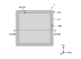
- FIG. 2 is a schematic plan view of the display device according to the first embodiment.
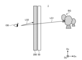
- FIG. 3 is a schematic side view showing the display device according to the first embodiment.
- FIG. 4 is a perspective view illustrating an example of a display unit according to the first embodiment.
- FIG. 5 is a timing chart for explaining the timing at which the light source emits light in the field sequential method of the display unit.
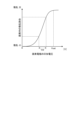
- FIG. 6 is an explanatory diagram showing the relationship between the voltage applied to the pixel electrodes of the display unit and the scattering state of the pixels.
- FIG. 7 is a cross-sectional view showing an example of a cross section of the display unit.
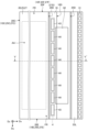
- FIG. 8 is a plan view showing the plane of the display unit in FIG. FIG.
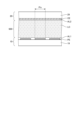
- FIG. 9 is an enlarged cross-sectional view of the liquid crystal layer portion of FIG.
- FIG. 10 is a cross-sectional view for explaining the non-scattering state in the liquid crystal layer.
- FIG. 11 is a cross-sectional view for explaining the scattering state in the liquid crystal layer.
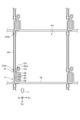
- FIG. 12 is a plan view showing scanning lines, signal lines, and switching elements in a pixel.
- FIG. 13 is a plan view showing a storage capacitor layer in a pixel.
- FIG. 14 is a plan view showing a pixel electrode in a pixel.
- FIG. 15 is a plan view showing a light-shielding layer in a pixel.
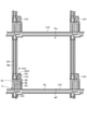
- FIG. 16 is a cross-sectional view taken along line XVI-XVI' of FIG. FIG.
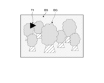
- FIG. 17 is an explanatory diagram illustrating an example in which the display panel is in the first state and the transmittance of the light control panel is high.
- FIG. 18 is an explanatory diagram illustrating an example in which the display panel is in the second state and the transmittance of the light control panel is low.
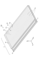
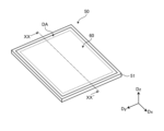
- FIG. 19 is a perspective view illustrating an example of a light adjusting unit according to the first embodiment.
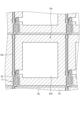
- FIG. 20 is a cross-sectional view taken along line XX-XX' of FIG. 19.
- FIG. 21 is an enlarged schematic cross-sectional view of the portion AX shown in FIG.
- FIG. 22 is a circuit diagram showing a dimming unit according to the first embodiment.
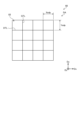
- FIG. 23 is a plan view showing pixels of a display panel according to the second embodiment.
- FIG. 24 is a plan view showing a segment of a light control panel according to the second embodiment.
- FIG. 25 is a plan view showing pixel electrodes of a display panel according to the third embodiment.
- FIG. 26 is a plan view showing the size of a first electrode of a light control panel according to the third embodiment.
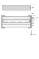
- FIG. 27 is a schematic cross-sectional view of a display device according to a comparative example.
- FIG. 28 is a schematic cross-sectional view of a display device according to the fourth embodiment.
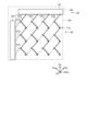
- FIG. 29 is a circuit diagram showing a dimming unit according to the fifth embodiment.
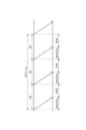
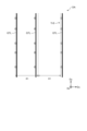
- FIG. 30 is a plan view showing a gate line according to the sixth embodiment.
- FIG. 31 is a plan view showing a drain wire according to the sixth embodiment.
- FIG. 1 is a block diagram showing a display device according to the first embodiment.
- FIG. 2 is a schematic plan view of the display device according to the first embodiment.
- the display device 1 includes a signal processing circuit 40, a display unit 200, and a dimming unit 50.
- one direction of the plane of the display device 1 is a first direction Dx
- a direction perpendicular to the first direction Dx is a second direction Dy
- a direction perpendicular to the Dx-Dy plane is a third direction Dz.
- “planar view” means viewing the display device 1 from the +Dz side toward the -Dz side along the third direction Dz. Note that the directions of Dx, Dy, and Dz are merely examples, and the present disclosure is not limited to these directions.
- the display unit 200 has a display panel 2, a light source 3 (see FIG. 7), and a drive circuit 4.
- the display panel 2 has an active area AA in which a plurality of pixels Pix are provided.
- the plurality of pixels Pix are arranged, for example, in a matrix.
- a row refers to a pixel row having m pixels Pix arranged in one direction.
- a column refers to a pixel column having n pixels Pix arranged in a direction perpendicular to the direction in which the rows are arranged.
- the values of m and n are determined according to the vertical display resolution and the horizontal display resolution.
- a plurality of scanning lines GL are wired for each row, and a plurality of signal lines SL are wired for each column.
- the light source 3 includes a plurality of light-emitting units 31.
- the light source control unit 32 is provided on a wiring board 93 (see FIG. 7).
- the wiring board 93 is a flexible printed circuit board or a PCB board.
- a light source control signal LCSA is sent to the light source control unit 32 from an image output unit 91 of an external higher-level control unit 9.
- the light source control signal LCSA is a signal that includes information on the amount of light of the light-emitting unit 31 that is set according to, for example, the input gradation value to the pixel Pix.
- the drive circuit 4 includes a pixel control circuit 42, a gate drive circuit 43, a source drive circuit 44, and a common potential drive circuit 45.
- the signal processing circuit 40 receives an input signal (such as an RGB signal) VS from the image output unit 91 of the external higher-level control unit 9 via a flexible printed circuit board 92.
- an input signal such as an RGB signal
- the signal processing circuit 40 includes an input signal analysis unit 411 and a signal adjustment unit 413.
- the input signal analysis unit 411 generates a second input signal VCS based on a first input signal VS input from the outside.
- the second input signal VCS is a signal that determines what gradation value is to be given to each pixel Pix of the display panel 2 based on the first input signal VS.
- the second input signal VCS is a signal that includes gradation information regarding the gradation value of each pixel Pix.
- the signal adjustment unit 413 generates a third input signal VCSA from the second input signal VCS.
- the signal adjustment unit 413 sends the third input signal VCSA to the pixel control circuit 42.
- the pixel control circuit 42 generates a horizontal drive signal HDS and a vertical drive signal VDS based on the third input signal VCSA.
- the horizontal drive signal HDS and the vertical drive signal VDS are generated for each color that the light emitting section 31 can emit.
- the gate drive circuit 43 sequentially selects the scanning lines GL of the display panel 2 within one vertical scanning period based on the horizontal drive signal HDS.
- the order in which the scanning lines GL are selected is arbitrary.
- the gate drive circuit 43 and the scanning lines GL are electrically connected by the first wiring GPL1 and the second wiring GPL2 arranged in the peripheral region FR (see FIG. 1) outside the active area AA.
- the source drive circuit 44 supplies a grayscale signal corresponding to the output grayscale value of each pixel Pix to each signal line SL of the display panel 2 within one horizontal scanning period based on the vertical drive signal VDS.
- the dimming unit 50 includes a dimming panel 60 and a dimming panel drive unit 140.
- the dimming panel 60 has a dimming area DA arranged at a position superimposed on the active area AA when the active area AA is viewed in a plan view, i.e., when the display device 1 is viewed from the third direction Dz.
- the dimming panel 60 controls the degree of light transmission within the dimming area DA.
- the dimming panel drive unit 140 includes a gate line selection circuit 141 and a drain line output circuit 142.
- a plurality of supply lines GTL connected to the gate line selection circuit 141 extend in the second direction Dy and are arranged side by side in the first direction Dx.
- a plurality of drain lines STL connected to the drain line output circuit 142 extend in the first direction Dx and are arranged side by side in the second direction Dy.
- the gate line selection circuit 141 is electrically connected to the dimming panel 60 by a plurality of supply lines GTL.
- the gate line selection circuit 141 sequentially or simultaneously selects the supply lines GTL of the dimming panel 60 and outputs a drive signal.
- the drain line output circuit 142 is electrically connected to the dimming panel 60 by a plurality of drain lines DTL.
- the drain line output circuit 142 drives the dimming panel 60 in response to the dimming signal DI.
- the signal processing circuit 40 performs various outputs based on the input signal IP input from the external higher-level control unit 9, and controls the operation of the dimming unit 50.
- the signal processing circuit 40 outputs a dimming signal DI generated based on the input signal IP to the dimming unit 50.
- FIG. 3 is a schematic side view showing the display device according to the first embodiment.
- an observer OB looks from the display panel 2 toward the dimming panel 60, if the observer OB views the background BG through the display panel 2, the line of sight is LS1. If the observer OB views the image displayed on the display panel 2, the line of sight is LS2.
- Fig. 4 is a perspective view showing an example of a display panel according to the present embodiment.
- Fig. 5 is a timing chart showing the timing at which the light source emits light in the field sequential method of the first embodiment.
- the display panel 2 has an active area AA in which an image can be displayed, and a peripheral area FR outside the active area AA.
- the drive circuit 4 is fixed to the surface of the array substrate 10.
- the array substrate 10 has a larger area in the Dx-Dy plane than the counter substrate 20, and the drive circuit 4 is provided on the protruding portion of the array substrate 10 that is exposed from the counter substrate 20.
- the display panel 2 is an active matrix type panel. Therefore, there are signal (source) lines SL extending in the second direction Dy and scanning (gate) lines GL extending in the first direction Dx in a plan view, and switching elements Tr are located at the intersections of the signal lines SL and the scanning lines GL.
- the switching element Tr is, for example, a thin film transistor.
- the thin film transistor may be, for example, a bottom gate transistor or a top gate transistor.
- a single gate thin film transistor is exemplified as the switching element Tr, but a double gate transistor may also be used.
- One of the source electrode and drain electrode of the switching element Tr is connected to the signal line SL, the gate electrode is connected to the scanning line GL, and the other of the source electrode and drain electrode is connected to one end of the capacitance of the polymer dispersed liquid crystal LC described later.
- One end of the capacitance of the polymer dispersed liquid crystal LC is connected to the switching element Tr via the pixel electrode PE, and the other end is connected to the common potential wiring COML via the common electrode CE.
- a retention capacitance HC is generated between the pixel electrode PE and the retention capacitance electrode ITO electrically connected to the common potential wiring COML.
- the common potential wiring COML is supplied from the common potential drive circuit 45.
- the light-emitting unit 31 includes a first color (e.g., red) light-emitting body 33R, a second color (e.g., green) light-emitting body 33G, and a third color (e.g., blue) light-emitting body 33B.
- the light source control unit 32 controls each of the first color light-emitting body 33R, the second color light-emitting body 33G, and the third color light-emitting body 33B to emit light in a time-division manner. In this way, the first color light-emitting body 33R, the second color light-emitting body 33G, and the third color light-emitting body 33B are driven by the field sequential method.
- the first color light emitter 33R emits light during the first color light emission period RON, and the pixel Pix selected within one vertical scanning period GateScan scatters the light to display.
- the entire display panel 2 if a gradation signal corresponding to the output gradation value of each pixel Pix is supplied to each of the signal lines SL described above for the pixel Pix selected within one vertical scanning period GateScan, then only the first color is lit during the first color light emission period RON.
- the second color light emitter 33G emits light during the second color light emission period GON, and the pixel Pix selected within one vertical scanning period GateScan scatters the light to display.
- the entire display panel 2 if a gradation signal corresponding to the output gradation value of each pixel Pix is supplied to each of the signal lines SL described above for the pixel Pix selected within one vertical scanning period GateScan, then only the second color is lit during the second color light emission period GON.
- the third color light emitter 33B emits light during the third color light emission period BON, and the pixel Pix selected within one vertical scanning period GateScan scatters the light to display.
- the entire display panel 2 if a gradation signal corresponding to the output gradation value of each pixel Pix is supplied to each of the signal lines SL described above for the pixel Pix selected within one vertical scanning period GateScan, then only the third color is lit during the third color light emission period BON.
- the human eye has a limited temporal resolution and an afterimage occurs, so a composite image of three colors is recognized during one frame (1F).
- the field sequential method does not require a color filter and reduces absorption loss in the color filter, achieving high transmittance.
- one pixel is made up of sub-pixels that divide the pixel Pix into a first color, a second color, and a third color, whereas the field sequential method does not require such sub-pixel division. It is also possible to further include a fourth sub-frame and emit a fourth color different from the first color, second color, and third color.
- FIG. 6 is an explanatory diagram showing the relationship between the voltage applied to the pixel electrode and the scattering state of the pixel.
- FIG. 7 is a cross-sectional view showing an example of a cross section of the display section.
- FIG. 8 is a plan view showing the plane of the display section of FIG. 4.
- FIG. 9 is an enlarged cross-sectional view of the liquid crystal layer portion of FIG. 7.
- FIG. 10 is a cross-sectional view for explaining the non-scattering state in the liquid crystal layer.
- FIG. 11 is a cross-sectional view for explaining the scattering state in the liquid crystal layer.
- a gradation signal corresponding to the output gradation value of each pixel Pix selected within one vertical scanning period GateScan is supplied to each of the signal lines SL described above, the voltage applied to the pixel electrode PE changes according to the gradation signal.
- the voltage applied to the pixel electrode PE changes, the voltage between the pixel electrode PE and the common electrode CE changes. Then, as shown in FIG. 6, the scattering state of the liquid crystal layer 500 for each pixel Pix is controlled according to the voltage applied to the pixel electrode PE, and the scattering ratio within the pixel Pix changes.
- the drive circuit 4 changes the voltage applied to the pixel electrode PE according to the vertical drive signal VDS in a voltage range Vdr that is lower than the saturation voltage Vsat.
- the display unit 200 includes a first light-transmitting substrate 25, a display panel 2, and a second light-transmitting substrate 27.
- a protective layer 75 is provided on one side of the first light-transmitting substrate 25.
- a protective layer 76 is provided on one side of the second light-transmitting substrate 27.
- the display panel 2 comprises an array substrate 10, a counter substrate 20, and a liquid crystal layer 500.
- the counter substrate 20 faces the surface of the array substrate 10 in a direction perpendicular to the surface (the third direction DZ shown in FIG. 1).
- the liquid crystal layer 500 is made of polymer-dispersed liquid crystal, which will be described later, sealed between the array substrate 10, the counter substrate 20, and a sealing portion 18.
- the array substrate 10 has a first main surface 10A, a second main surface 10B, a first side surface 10C, a second side surface 10D, a third side surface 10E, and a fourth side surface 10F.
- the first main surface 10A and the second main surface 10B are parallel planes.
- the first side surface 10C and the second side surface 10D are parallel planes.
- the third side surface 10E and the fourth side surface 10F are parallel planes.
- the opposing substrate 20 has a first main surface 20A, a second main surface 20B, a first side surface 20C, a second side surface 20D, a third side surface 20E, and a fourth side surface 20F.
- the first main surface 20A and the second main surface 20B are parallel planes.
- the first side surface 20C and the second side surface 20D are parallel planes.
- the third side surface 20E and the fourth side surface 20F are parallel planes.
- the first substrate 25 has a first main surface 25A, a second main surface 25B, a first side surface 25C, a second side surface 25D, a third side surface 25E, and a fourth side surface 25F.
- the first main surface 25A and the second main surface 25B are parallel planes.
- the first side surface 25C and the second side surface 25D are parallel planes.
- the third side surface 25E and the fourth side surface 25F are parallel planes.
- the first substrate 25 is attached to the first main surface 20A of the opposing substrate 20 via an optical resin 23.
- the first substrate 25 is a protective substrate for the opposing substrate 20, and is formed, for example, from glass or a light-transmitting resin.
- the first substrate 25 is formed from a glass substrate, it is also called a cover glass.
- the first substrate 25 is formed from a light-transmitting resin, it may be flexible.
- the second substrate 27 has a first main surface 27A, a second main surface 27B, a first side surface 27C, a second side surface 27D, a third side surface 27E, and a fourth side surface 27F.
- the first main surface 27A and the second main surface 27B are parallel planes.
- the first side surface 27C and the second side surface 27D are parallel planes.
- the third side surface 27E and the fourth side surface 27F are parallel planes.
- the second substrate 27 is attached to the first main surface 10A of the array substrate 10 via an optical resin 26.
- the second substrate 27 is a protective substrate for the array substrate 10, and is formed, for example, from glass or a light-transmitting resin.
- the second substrate 27 is formed from a glass substrate, it is also called a cover glass.
- the second substrate 27 is formed from a light-transmitting resin, it may be flexible.
- the light source 3 faces the second side surface 25D of the first substrate 25.
- the light source 3 is sometimes called a side light source.
- the light source 3 irradiates light source light to the second side surface 25D of the first substrate 25.
- the second side surface 25D of the first substrate 25 facing the light source 3 serves as a light incidence surface.
- the light incidence surface facing the light source 3 may also be the second side surface 20D of the opposing substrate 20 or the second side surface 27D of the second substrate 27.
- the light source 3 includes a light emitter 31 and a light guide 33L.
- the light emitter 31 includes a first color (e.g., red) light emitter 33R, a second color (e.g., green) light emitter 33G, and a third color (e.g., blue) light emitter 33B.
- the light guide 33L irradiates the light emitted by the first color light emitter 33R, the second color light emitter 33G, and the third color light emitter 33B to the second side surface 25D of the first base material 25.
- the light guide 33L simultaneously receives the light of the multiple light emitters 31, diffuses it internally, and releases it to the display panel 2. As a result, the distribution of light per unit area irradiated to the second side surface 25D of the first base material 25 is uniform.
- the light guide 33L is a single light guide 33L that is integrally formed from the third side 25E to the fourth side 25F.
- the light guide 33L may be configured by arranging a plurality of divided light guides from the third side 25E to the fourth side 25F.
- the light guide 33L may be configured by arranging a plurality of divided light guides from the third side 25E to the fourth side 25F, and connecting adjacent light guides.
- the light emitting section 31 and the light guide 33L are fixed with an adhesive or the like and assembled to the support 33M to form a light source module.
- the support 33M is mounted so as to overlap the first main surface 25A of the first base material 25 and is fixed to the first base material 25 with an adhesive or the like.
- the wiring board 93 (flexible printed circuit board or PCB board) is equipped with an integrated circuit of the light source control unit 32, and the light source control unit 32 is connected to the light source 3 via the wiring board 93 (flexible printed circuit board or PCB board).
- the wiring board 93 is fixed to the support body 33M with an adhesive or the like.
- the light source light emitted from the light source 3 propagates in a direction away from the second side surface 20D (second direction Dy) while being reflected by either the first substrate 25, the array substrate 10, the counter substrate 20, or the second substrate 27.
- the light source light L propagating through the first substrate 25, the array substrate 10, the counter substrate 20, or the second substrate 27 is scattered at the pixel Pix where the liquid crystal is in a scattering state, and the angle of incidence of the scattered light becomes smaller than the critical angle, so that radiated light 68, 68A is radiated to the outside from the first main surface 20A of the counter substrate 20 (the first main surface 25A of the first substrate 25) and the first main surface 10A of the array substrate 10, respectively.
- the radiated light 68, 68A radiated to the outside from the first main surface 20A of the counter substrate 20 and the first main surface 10A of the array substrate 10, respectively, is observed by the observer.
- multiple light-emitting units 31 are arranged at a predetermined pitch in an area of the active area AA that corresponds to the first direction Dx.
- the drive circuit 4 described above includes multiple integrated circuits for the gate drive circuit 43 and multiple integrated circuits for the source drive circuit 44.
- the array substrate 10 is provided with a first alignment film AL1.
- the counter substrate 20 is provided with a second alignment film AL2.
- the alignment film is subjected to an alignment treatment, for example, the alignment direction of the first alignment film AL1 is on one side of the first direction Dx, and the alignment direction of the second alignment film AL2 is on the other side of the first direction Dx.
- the first alignment film AL1 and the second alignment film AL2 may be, for example, vertical alignment films, or may be alignment films that are aligned in the first direction Dx in which the multiple light-emitting sections 31 are arranged.
- the alignment treatment is performed by a rubbing treatment or a photo-alignment treatment.
- the polymer-dispersed liquid crystal LC of the liquid crystal layer 500 shown in FIG. 10 is sealed between the array substrate 10 and the opposing substrate 20.
- the monomer is polymerized by ultraviolet light or heat to form a three-dimensional mesh-like polymer network 510.
- the polymer dispersed liquid crystal LC has a three-dimensional mesh-like polymer network 510 and liquid crystal molecules 520.
- the orientation of the liquid crystal molecules 520 is controlled by the voltage difference between the pixel electrode PE and the common electrode CE.
- the orientation of the liquid crystal molecules 520 changes depending on the voltage applied to the pixel electrode PE.
- the change in the orientation of the liquid crystal molecules 520 changes the degree of scattering of light passing through the pixel Pix.
- the optical axis Ax1 of the polymer network 510 and the optical axis Ax2 of the liquid crystal molecules 520 are oriented substantially the same.
- the optical axis Ax2 of the liquid crystal molecules 520 is parallel to the first direction Dx (FIG. 7) of the liquid crystal layer 500.
- the optical axis Ax1 of the polymer network 510 is also parallel to the first direction Dx of the liquid crystal layer 500 regardless of the presence or absence of voltage.
- the ordinary light refractive indexes of the polymer network 510 and the liquid crystal molecules 520 are equal to each other.
- the refractive index difference between the polymer network 510 and the liquid crystal molecules 520 is almost zero in all directions.
- the liquid crystal layer 500 is in a non-scattering state in which it does not scatter the light source light.
- the light source light propagates in a direction away from the light source 3 (light-emitting section 31).
- the background on the first major surface 20A side of the counter substrate 20 is visible from the first major surface 10A of the array substrate 10
- the background on the first major surface 10A side of the array substrate 10 is visible from the first major surface 20A of the counter substrate 20.
- the optical axis Ax2 of the liquid crystal molecules 520 is tilted by the electric field generated between the pixel electrode PE and the common electrode CE. Since the optical axis Ax1 of the polymer network 510 does not change due to the electric field, the optical axis Ax1 of the polymer network 510 and the optical axis Ax2 of the liquid crystal molecules 520 are oriented in different directions.
- the light source light is scattered. As described above, a portion of the scattered light source light is emitted to the outside from the first main surface 10A of the array substrate 10 or the first main surface 20A of the counter substrate 20, and this light is observed by the observer.
- a pixel Pix having a pixel electrode PE to which no voltage is applied the background on the first main surface 20A side of the counter substrate 20 is visible from the first main surface 10A of the array substrate 10, and the background on the first main surface 10A side of the array substrate 10 is visible from the first main surface 20A of the counter substrate 20.
- a first input signal VS is input from the image output unit 91
- a voltage is applied to the pixel electrode PE of the pixel Pix where an image is displayed, and an image based on the third input signal VCSA is visible together with the background.
- the polymer dispersed liquid crystal LC is in a scattering state, an image is displayed in the display area.
- the image displayed by the light emitted to the outside after scattering the light source in a pixel Pix having a pixel electrode PE to which a voltage is applied is superimposed on the background.
- the display device 1 of this embodiment can display an image superimposed on the background by combining the radiated light 68 or radiated light 68A with the background.
- each pixel electrode PE in one vertical scanning period GateScan shown in FIG. 5, the potential of each pixel electrode PE (see FIG. 9) that has been written must be held during at least one of the first color light emission period RON, the second color light emission period GON, and the third color light emission period BON that follow each vertical scanning period GateScan. If the potential of each pixel electrode PE (see FIG. 8) that has been written cannot be held during at least one of the first color light emission period RON, the second color light emission period GON, and the third color light emission period BON that follow each vertical scanning period GateScan, so-called flicker is likely to occur.
- FIG. 12 is a plan view showing the scanning lines, signal lines, and switching elements in a pixel.
- FIG. 13 is a plan view showing the storage capacitance layer in a pixel.
- FIG. 14 is a plan view showing the pixel electrode in a pixel.
- FIG. 15 is a plan view showing the light-shielding layer in a pixel.
- FIG. 16 is a cross-sectional view of XIV-XIV' in FIG. 15.
- the array substrate 10 has a plurality of signal lines SL and a plurality of scanning lines GL arranged in a grid pattern in a plan view.
- one surface of the array substrate 10 has a plurality of signal lines SL arranged at intervals in the first direction Dx, and a plurality of scanning lines GL arranged at intervals in the second direction Dy.
- the area surrounded by adjacent scanning lines GL and adjacent signal lines SL is a pixel Pix.
- the pixel Pix is provided with a pixel electrode PE and a switching element Tr.
- the switching element Tr is a bottom-gate type thin-film transistor.
- the switching element Tr has a semiconductor layer SC that overlaps, in a planar view, with a gate electrode GE that is electrically connected to the scanning line GL.
- the scanning line GL is wiring made of a metal such as molybdenum (Mo) or aluminum (Al), a laminate of these, or an alloy of these.
- the signal line SL is wiring made of a metal such as aluminum or an alloy.
- the semiconductor layer SC is arranged so as not to protrude from the gate electrode GE in a plan view. This allows the light source light L directed from the gate electrode GE side toward the semiconductor layer SC to be reflected, making it difficult for light leakage to occur in the semiconductor layer SC.
- the light source light L emitted from the light source 3 is incident in the second direction Dy.
- the incident direction is the direction from the second side 20D closest to the light source 3 to the first side 20C which is the opposing surface of the second side 20D.
- the length of the semiconductor layer SC in the first direction is smaller than the length of the semiconductor layer SC in the first direction Dx. This reduces the length of the light source light L in the direction intersecting the incident direction, reducing the effect of light leakage.
- the source electrode SE is made of the same two conductors as the signal line SL, and extends from the signal line SL in the same layer as the signal line SL and in a direction intersecting the signal line. As a result, the source electrode SE, which is electrically connected to the signal line SL, overlaps one end of the semiconductor layer SC in a plan view.
- a drain electrode DE is provided between the conductors of adjacent source electrodes SE.
- the drain electrode DE overlaps with the semiconductor layer SC.
- the portion that does not overlap with the source electrode SE and the drain electrode DE functions as the channel of the switching element Tr.
- the contact electrode DEA electrically connected to the drain electrode DE is electrically connected to the pixel electrode PE through a contact hole CH.
- the array substrate 10 has a first light-transmissive substrate 19 made of, for example, glass.
- the first light-transmissive substrate 19 may be a resin such as polyethylene terephthalate, so long as it has light-transmissive properties.
- the scanning line GL (see FIG. 10) and the gate electrode GE are provided on the first light-transmissive substrate 19.
- a first insulating layer 11 is provided to cover the scanning line GL and the gate electrode GE.
- the first insulating layer 11 is formed of a transparent inorganic insulating material such as silicon nitride.
- a semiconductor layer SC is laminated on the first insulating layer 11.
- the semiconductor layer SC is formed of, for example, amorphous silicon, but may be formed of polysilicon or an oxide semiconductor.
- the length Lsc of the semiconductor layer SC is smaller than the length Lge of the gate electrode GE overlapping the semiconductor layer SC. This allows the gate electrode GE to block the light Ld1 propagating through the first light-transmitting substrate 19. As a result, the switching element Tr of embodiment 1 has reduced light leakage.
- the second insulating layer 12 is formed, for example, from a transparent inorganic insulating material such as silicon nitride, similar to the first insulating layer.
- a third insulating layer is formed on the second insulating layer 12, covering a portion of the second insulating layer 12.
- the third insulating layer 13 is formed of an organic insulating material having translucency, such as an acrylic resin.
- the third insulating layer 13 has a thickness greater than other insulating films formed of inorganic materials.
- a metal layer TM is provided on the third insulating layer 13.
- the conductive metal layer TM is a metal such as molybdenum (Mo) or aluminum (Al), a laminate of these, or wiring of an alloy of these.
- the metal layer TM is provided in an area that overlaps the signal line SL, the scanning line GL, and the switching element Tr in a plan view. This gives the metal layer TM a lattice shape, and creates an opening AP surrounded by the metal layer TM.
- a storage capacitance electrode ITO is provided on the third insulating layer 13 and the metal layer TM.
- the storage capacitance electrode ITO is formed of a translucent conductive material such as ITO (Indium Tin Oxide).
- the storage capacitance electrode ITO is also called a third translucent electrode.
- the storage capacitance electrode ITO has an area IOX surrounded by the scanning line GL and the signal line SL where there is no translucent conductive material.
- the storage capacitance electrode ITO is provided across multiple pixels Pix, straddling adjacent pixels Pix. The area of the storage capacitance electrode ITO where there is a translucent conductive material overlaps the scanning line GL or the signal line SL, and extends to the adjacent pixel Pix.
- the storage capacitance electrode ITO is in a lattice shape that covers the scanning lines GL and signal lines SL along the scanning lines GL and signal lines SL. This reduces the storage capacitance HC between the region IOX without the translucent conductive material and the pixel electrode PE, so the storage capacitance HC is adjusted according to the size of the region IOX without the translucent conductive material.
- a switching element Tr is provided that is connected to a scanning line GL and a signal line SL. At least the switching element Tr is covered with a third insulating layer 13, which is an organic insulating layer, and above the third insulating layer 13 is a metal layer TM that has a larger area than the switching element Tr. This makes it possible to suppress light leakage from the switching element Tr.
- the array substrate 10 includes a third insulating layer 13, which is an organic insulating layer that covers at least the switching element Tr, and a metal layer TM that is provided above the third insulating layer 13 and has an area larger than that of the switching element Tr.
- a third insulating layer 13 which is an organic insulating layer that covers at least the switching element Tr, and a metal layer TM that is provided above the third insulating layer 13 and has an area larger than that of the switching element Tr.
- a third insulating layer 13 which is an organic insulating layer that covers at least the switching element Tr, and a metal layer TM that is provided above the third insulating layer 13 and has an area larger than that of the switching element Tr.
- the light source light L irradiated from the light source 3 is incident with the second direction Dy as the incident direction.
- the above-mentioned slope includes a first slope 13F of the third insulating layer 13 on the side where the light Lu of the light source light L is incident, and a second slope 13R of the third insulating layer 13 on the opposite side to the side where the light Lu is incident.
- the first slope 13F of the third insulating layer 13 on the side where the light Lu is incident is covered with a metal layer TMt.
- the metal layer TMt is made of the same material as the metal layer TM, and is a tapered portion formed by extending the metal layer TM.
- Light Lu arrives in the incident direction.
- Light Lu is a portion of the light source light L that arrives from the side closer to the light source 3 than the switching element Tr.
- the metal layer TMt blocks the light Lu, thereby reducing light leakage.
- the second slope 13R is covered with a metal layer TM and the background of the opposing substrate 20 is visible from the array substrate 10, the light Ld2 seen by the observer may be reflected by the metal layer TM covering the second slope 13R, and the reflected light may be visible to the observer.
- the metal layer TM may be on the storage capacitance electrode ITO, and may be laminated with the storage capacitance electrode ITO.
- the metal layer TM has a smaller electrical resistance than the storage capacitance electrode ITO. This reduces the variation in the potential of the storage capacitance electrode ITO depending on the position of the pixel Pix in the active area AA.
- a fourth insulating layer 14 is provided on the storage capacitance electrode ITO and the metal layer TM.
- the fourth insulating layer 14 is an inorganic insulating layer formed of a transparent inorganic insulating material such as silicon nitride.
- a pixel electrode PE is provided on the fourth insulating layer 14.
- the pixel electrode PE is made of a light-transmitting conductive material such as ITO.
- the pixel electrode PE is electrically connected to the contact electrode DEA via a contact hole CH provided in the fourth insulating layer 14, the third insulating layer 13, and the second insulating layer 12.
- the pixel electrode PE is partitioned for each pixel Pix.
- a first alignment film AL1 is provided on the pixel electrode PE.
- the counter substrate 20 has a second light-transmitting substrate 29 made of, for example, glass.
- the second light-transmitting substrate 29 may be a resin such as polyethylene terephthalate as long as it has light-transmitting properties.
- a common electrode CE is provided on the second light-transmitting substrate 29.
- the common electrode CE is made of a light-transmitting conductive material such as ITO.
- a second alignment film AL2 is provided on the surface of the common electrode CE.
- the counter substrate 20 also has a light-shielding layer LS between the second light-transmitting substrate 29 and the common electrode CE.
- the light-shielding layer LS is made of a black resin or metal material.
- a spacer PS is also formed between the array substrate 10 and the counter substrate 20, and the spacer PS is between the common electrode CE and the second alignment film AL2.
- a light-shielding layer GS which is in the same layer as the scanning line GL, extends along the signal line SL and is provided at a position overlapping with a part of the signal line SL.
- the light-shielding layer GS is made of the same material as the scanning line GL.
- the light-shielding layer GS is not provided at the portion where the scanning line GL and the signal line SL intersect in a plan view.
- the light-shielding layer GS and the signal line SL are electrically connected by a contact hole CHG. This reduces the wiring resistance of the light-shielding layer GS and the signal line SL compared to the wiring resistance of only the signal line SL. As a result, delay of the grayscale signal supplied to the signal line SL is suppressed. Note that the light-shielding layer GS and the signal line SL do not necessarily have to be connected without the contact hole CHG.
- the opposing substrate 20 is provided with a light-shielding layer LS.
- the light-shielding layer LS is provided in an area that overlaps the signal lines SL, the scanning lines GL, and the switching elements Tr in a plan view.
- the light-shielding layer LS has a width greater than that of the metal layer TM. This prevents light reflected at the edges of the signal lines SL, scanning lines GL, and metal layer TM from being emitted from the display panel 2. As a result, the visibility of images in the display device 1 is improved.
- the contact holes CH and CHG are prone to diffuse reflection when exposed to light source light L. For this reason, the light-shielding layer LS is provided in an area that overlaps the contact holes CH and CHG in a plan view.
- spacers SP are disposed between the array substrate 10 and the opposing substrate 20, improving the uniformity of the distance between the array substrate 10 and the opposing substrate 20.
- FIG. 17 is an explanatory diagram illustrating an example in which the display panel is in a first state and the light control panel has a high transmittance.
- FIG. 18 is an explanatory diagram illustrating an example in which the display panel is in a second state and the light control panel has a low transmittance.
- the processing area BS is not the entire area of the active area AA, but a part of the active area AA.
- the first state refers to a state in which the liquid crystal layer 500 is in a non-scattering state, and the background BG is visible without the pixel Pix scattering light.
- the second state refers to a state in which the liquid crystal layer 500 is in a scattering state, and the pixel Pix scatters light to display the image T1.
- the degree of light transmission in the dimming area DA of the dimming panel 60 is at its highest.
- the second state the degree of light transmission in the dimming area DA of the dimming panel 60 is at its lowest.
- Fig. 19 is a perspective view showing an example of a dimming unit according to the first embodiment.
- Fig. 20 is a cross-sectional view taken along the line XX-XX' in Fig. 19.
- Fig. 21 is a schematic cross-sectional view showing an enlarged view of the AX portion shown in Fig. 20.
- Fig. 22 is a circuit diagram showing a dimming unit according to the first embodiment.
- the dimming unit 50 has a frame 51 and a dimming panel 60.
- the dimming panel 60 is fixed by surrounding the peripheral portion of the dimming panel 60 with the frame 51.
- the dimming panel 60 has a first substrate 610, a second substrate 620, a circuit forming layer 630, a first electrode 61, a second electrode 62, an electrochromic layer 71, and a sealing portion 72.
- the dimming panel 60 is layered in the following order: the first substrate 610, the circuit forming layer 630, the first electrode 61, the electrochromic layer 71, and the second substrate 620.
- the first substrate 610 and the second substrate 620 are substrates having translucency.
- the first substrate 610 and the second substrate 620 are, for example, glass substrates.
- the first substrate 610 and the second substrate 620 are not limited to this, and may be substrates formed using, for example, a translucent resin.
- the first electrode 61 is an anode electrode.
- the first electrode 61 is made of a translucent conductive material such as ITO (Indium Tin Oxide).
- the second electrode 62 is a cathode electrode.
- the second electrode 62 is formed of a translucent conductive material such as ITO or IZO.
- the second electrode 62 is formed continuously across the entire dimming area DA.
- the second electrode 62 faces the multiple first electrodes 61 with the electrochromic layer 71 sandwiched between them.
- the circuit formation layer 630 is provided on the first substrate 610, and is a layer in which various wiring such as various transistors including the switching element TrS shown in Figures 21 and 22 is formed.
- the electrochromic layer 71 contains an electrochromic material and an electrolyte.
- the electrolyte of the electrochromic layer 71 is an electrolyte solution provided corresponding to the electrochromic material.
- the electrochromic material is a material containing an ion-inserted metal oxide.
- the electrochromic material is tungsten oxide (WO 3 )
- the electrolyte is an aqueous electrolyte solution such as sulfuric acid or water, or an organic electrolyte solution containing a lithium salt.
- an oxidation-reduction reaction is caused in which hydrogen ions (H + ) or lithium salt ions (Li + ) move between the electrochromic material and the electrolyte, and the degree of light transmission of the electrochromic material changes.
- the electrochromic material is not limited to this, and other materials that cause an electrochromic oxidation-reduction reaction may be adopted.
- the sealing portion 72 is provided so as to surround the periphery of the electrochromic layer 71.
- the electrochromic layer 71 is sealed within the dimming area DA by the first substrate 610, the second substrate 620, and the sealing portion 72.
- the sealing portion 72 effectively seals the electrochromic layer 71 and can prevent moisture from entering from the outside.
- the dimming panel 60 is a dimming panel that is provided so that the degree of electrochromic material and the degree of coloring can be reversibly controlled by controlling the presence or absence of a potential difference between the first electrode 61 and the second electrode 62.
- the dimming panel 60 is controlled so that the electrochromic material has either the highest degree of light transmittance or the lowest degree of light transmittance.
- the specific light transmittance of the dimming panel 60 corresponds to the electrochromic material.
- the circuit formation layer 630 is formed on the first substrate 610 by stacking the light-shielding layer 63, the insulating film 81, the light-shielding layer 310, the overcoat layer 320, the insulating film 330, and the first electrode 61 in this order in the third direction Dz.
- the insulating film 81 has a first insulating film 81a, a second insulating film 81b, and a third insulating film 81c.
- the insulating film 81 is laminated on the sensor substrate 210 in the order of the first insulating film 81a, the second insulating film 81b, and the third insulating film 81c.
- the first insulating film 81a is provided on the sensor substrate 210, covering the light-shielding layer 63.
- the switching element TrS is provided on the first insulating film 81a.
- the switching element TrS has a semiconductor layer 64, a source electrode 65, a drain electrode 66, and a gate electrode 67.
- the light-shielding layer 63 may be electrically connected to the gate electrode 67, and the light-shielding layer 63 may function as the gate electrode.
- the switching element TrS is, for example, a thin film transistor.
- the switching element TrS controls the potential difference between the first electrode 61 and the second electrode 62.
- the thin film transistor may be, for example, a bottom gate transistor or a top gate transistor.
- a double gate thin film transistor is exemplified as the switching element TrS, but a single gate transistor may also be used.
- the second insulating film 81b is provided on the first insulating film 81a, covering the semiconductor layer 64.
- the gate electrode 67 is provided on the second insulating film 81b.
- the light-shielding layer 63 overlaps the semiconductor layer 64 and the gate electrode 67 when viewed from the third direction Dz, and is provided in a layer different from the semiconductor layer 64 and the gate electrode 67.
- the third insulating film 38c is provided on the second insulating film 38b, covering the gate electrode 67.
- the source electrode 65 is provided on one end side of the semiconductor layer 64 on the third insulating film 38c.
- the drain electrode 66 is provided on the other end side of the semiconductor layer 64 on the third insulating film 38c.
- the source electrode 65 faces the drain electrode 66 in the first direction Dx, sandwiching the gate electrode 67 therebetween.
- the first insulating film 38a, the second insulating film 38b, and the third insulating film 38c are formed of an inorganic material having translucency, such as silicon oxide or silicon nitride, for example.
- the semiconductor layer 64 is made of, for example, polysilicon.
- the semiconductor layer 64 is not limited to this and may be made of a microcrystalline oxide semiconductor, an amorphous oxide semiconductor, low temperature polysilicon (LTPS: Low Temperature Polycrystalline Silicone), etc.
- LTPS Low Temperature Polycrystalline Silicone
- One end of the semiconductor layer 64 is connected to the source electrode 65 via contact hole CH2.
- the other end of the semiconductor layer 64 is connected to the drain electrode 66 via contact hole CH3.
- the first electrode 61 is connected to the other end of the drain electrode 66 via contact hole CH1. With this configuration, the drain electrode 66 of the switching element TrS is electrically connected to the first electrode 61.
- the light-shielding layer 310 is disposed at a position overlapping the switching element TrS.
- the light-shielding layer 310 is provided on the third insulating film 38c in the third direction Dz so as to cover the entire source electrode and part of the drain electrode.
- the light-shielding layer 310 is formed of a black resin material.
- the light-shielding layer 310 blocks the light source light L1, so even if the observer OB views the active area AA of the display unit 200 in the third direction Dz, glare caused by the light source light L1 being reflected by the switching element TrS can be suppressed.
- the overcoat layer 320 covers the source electrode 65, the drain electrode 66, and the third insulating film 38c.
- the overcoat layer 320 is made of an inorganic material that is translucent.
- the insulating film 330 is provided on the overcoat layer 320.
- the insulating film 330 is formed of an inorganic material having translucency, such as silicon oxide or silicon nitride.
- each segment 83 has a switching element TrS.
- the gate electrode 67 of the switching element TrS is connected to the supply line GTL.
- the source electrode 65 of the switching element TrS is connected to the drain line DTL.
- the drain electrode 66 of the switching element TrS is connected to the first electrode 61.
- each supply line GTL connected to the gate line selection circuit 141 is branched into two lines at a position before the supply line GTL is first connected to the switching element TrS.
- the supply line GTL has first gate lines G1, G3 and second gate lines G2, G4.
- Each drain line DTL connected to the drain line output circuit 142 has a first drain line D1, a second drain line D2, a third drain line D3 and a fourth drain line D4. Note that the number of supply lines GTL and drain lines DTL is not limited to this, and each may be four or more.
- the gate line selection circuit 141 selects one of the first gate lines G1, G3 and the second gate lines G2, G4. As a result, the drive signal output from the gate line selection circuit 141 is supplied to the selected one of the first gate lines G1, G3 and the second gate lines G2, G4.
- the number of switching elements TrS may be doubled without increasing the portion where the supply line GTL is connected to the gate line selection circuit 141, thereby reducing the surface area of the switching elements TrS. This makes it difficult to see the switching elements TrS of the dimming panel 60 when viewing the display device 1, improving the appearance of the display device 1.
- the number of branches may be two or more.
- Fig. 23 is a plan view showing a pixel of a display panel according to embodiment 2.
- Fig. 24 is a plan view showing a segment of a light control panel according to embodiment 2.
- the width in the first direction Dx is Xtdp
- the height in the second direction Dy is Ytdp.
- the width in the first direction Dx is Xedp
- the height in the second direction Dy is Yedp.
- the length of the horizontal width Xtdp is greater than the horizontal width Xedp
- the length of the vertical width Ytdp is greater than the vertical width Yedp.
- the area of the segment 83 is greater than the area of the pixel Pix.
- the area of the segment 83 is, for example, approximately 10 times or more larger than the area of the pixel Pix. This makes the resolution of the dimming panel 60 coarser than the resolution of the display panel 2, improving the visibility of the displayed image.
- Fig. 25 is a plan view showing a pixel electrode of a display panel according to embodiment 1.
- Fig. 26 is a plan view showing the size of a first electrode of a light control panel according to embodiment 1.
- the width in the first direction Dx is Xtd
- the width in the second direction Dy is Ytd.
- the width in the first direction Dx is Xed
- the width in the second direction Dy is Yed.
- the length of the horizontal width Xtd is greater than the horizontal width Xed
- the length of the vertical width Ytd is greater than the vertical width Yed.
- the area of each first electrode is greater than the area of the pixel electrode PE partitioned for each pixel Pix.
- Fig. 27 is a schematic cross-sectional view of a display device according to Comparative Example 1.
- Fig. 28 is a schematic cross-sectional view of a display device according to Embodiment 2.
- Fig. 28 is a cross-sectional view taken along line XXVIII-XXVIII' in Fig. 2.
- the same components as those described in the above-mentioned embodiments are designated by the same reference numerals, and duplicated description will be omitted.
- the dimming panel 60A of the display device 1A according to Comparative Example 1 is stacked in the order of the second substrate 620, the second electrode 62, the electrochromic layer 71, the first electrode 61, the circuit-forming layer 630, and the first substrate 610.
- the circuit-forming layer 630 is disposed closer to the display unit 200 than in the dimming panel 60 of the first embodiment.
- the dimming panel 60 of the display device 1 according to embodiment 1 is stacked in the order of the second substrate 620, the second electrode 62, the electrochromic layer 71, the first electrode 61, the circuit-forming layer 630, and the first substrate 610.
- the circuit-forming layer 630 including the switching element TrS is disposed at a position separated from the display unit 200 via the electrochromic layer 71, thereby reducing moire caused by optical interference.
- a gap SP1 is provided between the display unit 200 and the light control panel 60.
- the gap SP1 is, for example, an air layer.
- the light source light L emitted from the light emitting unit 31 of the display unit 200 propagates in a direction away from the second side surface 20D while being reflected by the first main surface 10A of the array substrate 10 (see FIG. 7). Because a gap SP1 is provided between the display unit 200 and the dimming panel 60, even if the light source light L travels toward the dimming panel 60 through the gap SP1, it travels from a medium with a large refractive index to a medium with a small refractive index, and the light source light L is totally reflected by the first main surface 10A of the array substrate 10. This makes it possible to prevent the light source light L from entering the dimming panel 60.
- (Embodiment 5) 29 is a circuit diagram showing a dimming unit according to the fifth embodiment.
- the same components as those described in the above-mentioned embodiment are denoted by the same reference numerals, and duplicated description is omitted.
- a direction that does not intersect with any of the first direction Dx and the second direction Dy is defined as a fourth direction Dp
- a direction that does not intersect with any of the first direction Dx, the second direction Dy, and the fourth direction Dp is defined as a fifth direction Ds.
- the supply lines GTL extend in a zigzag pattern along the fourth direction Dp and the fifth direction Ds, and are arranged at intervals in the first direction Dx.
- the drain lines DTL extend in a zigzag pattern along the fourth direction Dp and the fifth direction Ds, and are arranged at intervals in the second direction Dy.
- the supply lines GTL and drain lines DTL of the dimming panel 60 are not parallel to the direction of the wiring in which the scanning lines GL and signal lines SL of the display panel 2 are arranged, so that the wiring of the dimming panel 60 and the display panel 2 do not overlap, reducing moire caused by optical interference.
- Fig. 30 is a plan view showing a supply line according to embodiment 6.
- Fig. 31 is a plan view showing a drain line according to embodiment 6.
- three supply lines GTL are arranged at a predetermined interval in the first direction Dx in the dimming area DA.
- the number of supply lines GTL is not limited to three, and may be three or more.
- the average pitch X1 is calculated by adding up the intervals between adjacent supply lines GTL and dividing the sum by the number of supply lines GTL.
- the interval between adjacent supply lines GTL differs from the average pitch X1.
- the entire interval between adjacent supply lines GTL does not have to differ from the average pitch X1, and a portion of the interval between adjacent supply lines GTL may be the same as the average pitch X1.
- five drain lines DTL are arranged at a predetermined interval in the second direction Dy in the dimming area DA.
- the number of drain lines DTL is not limited to five, and may be three or more.
- the average pitch Y1 is calculated by adding up the intervals between adjacent drain lines DTL and dividing the sum by the number of drain lines DTL.
- the drain lines DTL are arranged at the average pitch Y1 in the second direction Dy based on the switching element TrS arranged on one drain line DTL, the interval between adjacent drain lines DTL differs from the average pitch Y1.
- the entire interval between adjacent drain lines DTL does not have to differ from the average pitch Y1, and a portion of the interval between adjacent drain lines DTL may be the same as the average pitch Y1.
- REFERENCE SIGNS LIST 1 display device 2 display panel 60 dimming panel 61 first electrode 62 second electrode 65 source electrode 66 drain electrode 67 gate electrode 71 electrochromic layer 83 segment 310 light shielding layer 320 overcoat layer 610 first substrate 620 second substrate AA active area DA dimming area GL scanning line SL signal line SP1 gap GTL supply line DTL drain line Tr, TrS switching element
Landscapes
- Physics & Mathematics (AREA)
- Nonlinear Science (AREA)
- General Physics & Mathematics (AREA)
- Optics & Photonics (AREA)
- Chemical & Material Sciences (AREA)
- Mathematical Physics (AREA)
- Crystallography & Structural Chemistry (AREA)
- Engineering & Computer Science (AREA)
- Dispersion Chemistry (AREA)
- Microelectronics & Electronic Packaging (AREA)
- Theoretical Computer Science (AREA)
- Devices For Indicating Variable Information By Combining Individual Elements (AREA)
Abstract
表示する画像の視認性を向上させることができる表示装置を提供する。表示装置は、複数の画素が設けられたアクティブ領域を有し、アクティブ領域において、画素が第1状態にあるとき背景が視認され、画素が第2状態にあるとき画像を表示する表示パネルと、アクティブ領域に、平面視で重畳する位置に配置された調光領域を有し、調光領域内における透光の度合いを制御可能に設けられた調光パネルと、を備え、調光パネルは、第1電極と、エレクトロクロミック層を挟んで、第1電極に対向する第2電極を有する。
Description
本開示は、表示装置に関する。
印加電圧に応じて透光の度合いと着色の度合いを制御可能な領域を形成できるエレクトロクロミック素子が知られている(例えば特許文献1)。
このようなエレクトロクロミック素子を用いた調光パネルと、表示パネルを重ね合わせて使用する場合、調光パネルのアクティブ基板上に設けられた駆動素子に接続された配線と、アクティブマトリクス型パネル内に設けられた駆動素子に接続された配線とが重なってしまうことで、表示する画像の視認性が低下する可能性がある。
本発明は、表示する画像の視認性を向上させることができる表示装置を提供することを目的とする。
本開示の一態様による表示装置は、複数の画素が設けられたアクティブ領域を有し、前記アクティブ領域において、前記画素が第1状態にあるとき背景が視認され、前記画素が第2状態にあるとき画像を表示する表示パネルと、前記アクティブ領域に、平面視で重畳する位置に配置された調光領域を有し、前記調光領域内における透光の度合いを制御可能に設けられた調光パネルと、を備え、前記調光パネルは、第1電極と、エレクトロクロミック層を挟んで、前記第1電極に対向する第2電極を有する。
以下に、本開示の各実施の形態について、図面を参照しつつ説明する。なお、開示はあくまで一例にすぎず、当業者において、発明の主旨を保っての適宜変更について容易に想到し得るものについては、当然に本開示の範囲に含有されるものである。また、図面は説明をより明確にするため、実際の態様に比べ、各部の幅、厚さ、形状等について模式的に表される場合があるが、あくまで一例であって、本開示の解釈を限定するものではない。また、本明細書と各図において、既出の図に関して前述したものと同様の要素には、同一の符号を付して、詳細な説明を適宜省略することがある。
(実施形態1)
(表示装置の構成)
図1は、実施形態1に係る表示装置を示すブロック図である。図2は、実施形態1に係る表示装置の模式平面図である。図1に示すように、表示装置1は、信号処理回路40と、表示部200と、調光部50と、を備える。ここで、表示装置1の平面の一方向を第1方向Dxとし、第1方向Dxと直交する方向を第2方向Dyとし、Dx-Dy平面に直交する方向を第3方向Dzとする。また、「平面視」とは、第3方向Dzに沿って+Dz側から-Dz側に向かって表示装置1を見ることである。なお、Dx、Dy、Dzの方向は一例であって、本開示はこれらの方向に限定されない。
(表示装置の構成)
図1は、実施形態1に係る表示装置を示すブロック図である。図2は、実施形態1に係る表示装置の模式平面図である。図1に示すように、表示装置1は、信号処理回路40と、表示部200と、調光部50と、を備える。ここで、表示装置1の平面の一方向を第1方向Dxとし、第1方向Dxと直交する方向を第2方向Dyとし、Dx-Dy平面に直交する方向を第3方向Dzとする。また、「平面視」とは、第3方向Dzに沿って+Dz側から-Dz側に向かって表示装置1を見ることである。なお、Dx、Dy、Dzの方向は一例であって、本開示はこれらの方向に限定されない。
図1に示すように、表示部200は、表示パネル2、光源3(図7参照)及び駆動回路4を有する。表示パネル2は、複数の画素Pixが設けられたアクティブ領域AAを有する。複数の画素Pixは、例えばマトリクス状に配置されている。なお、本開示において、行とは、一方向に配列されるm個の画素Pixを有する画素行をいう。また、列とは、行が配列される方向と直交する方向に配列されるn個の画素Pixを有する画素列をいう。そして、mとnとの値は、垂直方向の表示解像度と水平方向の表示解像度に応じて定まる。また、複数の走査線GLが行毎に配線され、複数の信号線SLが列毎に配線されている。
光源3は、複数の発光部31を備えている。光源制御部32は、配線基板93(図7参照)上に、設けられる。配線基板93は、フレキシブルプリント基板又はPCB基板である。光源制御部32には、外部の上位制御部9の画像出力部91から光源制御信号LCSAが送出される。光源制御信号LCSAは、例えば、画素Pixへの入力階調値に応じて設定される発光部31の光量の情報を含む信号である。
駆動回路4は、画素制御回路42と、ゲート駆動回路43と、ソース駆動回路44と、共通電位駆動回路45と、を備える。
信号処理回路40には、外部の上位制御部9の画像出力部91から、フレキシブルプリント基板92を介して、入力信号(RGB信号など)VSが入力される。
信号処理回路40は、入力信号解析部411と、信号調整部413とを備える。入力信号解析部411は、外部から入力された第1入力信号VSに基づいて第2入力信号VCSを生成する。
第2入力信号VCSは、第1入力信号VSに基づいて、表示パネル2の各画素Pixにどのような階調値を与えるかを定める信号である。言い換えると、第2入力信号VCSは、各々の画素Pixの階調値に関する階調情報を含む信号である。
信号調整部413は、第2入力信号VCSから第3入力信号VCSAを生成する。信号調整部413は、第3入力信号VCSAを画素制御回路42へ送出する。
そして、画素制御回路42は、第3入力信号VCSAに基づいて水平駆動信号HDSと垂直駆動信号VDSとを生成する。本実施形態では、フィールドシーケンシャル方式で駆動されるので、水平駆動信号HDSと垂直駆動信号VDSとが発光部31が発光可能な色毎に生成される。
ゲート駆動回路43は水平駆動信号HDSに基づいて1垂直走査期間内に表示パネル2の走査線GLを順次選択する。走査線GLの選択の順番は任意である。ゲート駆動回路43と、走査線GLとは、アクティブ領域AAの外側の周辺領域FR(図1参照)に配置された第1配線GPL1及び第2配線GPL2で電気的に接続されている。
ソース駆動回路44は垂直駆動信号VDSに基づいて1水平走査期間内に表示パネル2の各信号線SLに各画素Pixの出力階調値に応じた階調信号を供給する。
調光部50は、調光パネル60と、調光パネル駆動部140と、を備える。図2に示すように、調光パネル60は、アクティブ領域AAを平面視した場合に、すなわち、第3方向Dzから表示装置1を見た場合に、アクティブ領域AAに重畳する位置に配置された調光領域DAを有する。調光パネル60は、透光の度合いを調光領域DA内で制御する。
調光パネル駆動部140は、ゲート線選択回路141及びドレイン線出力回路142を備える。ゲート線選択回路141に接続された、複数の供給線GTLは、第2方向Dyに延在して、第1方向Dxに並んで配置されている。ドレイン線出力回路142に接続された、複数のドレイン線STLは、第1方向Dxに延在して、第2方向Dyに並んで配置されている。
ゲート線選択回路141は、複数の供給線GTLによって調光パネル60と電気的に接続されている。ゲート線選択回路141は、調光パネル60の供給線GTLを順次又は同時に選択し、駆動信号を出力する。
ドレイン線出力回路142は、複数のドレイン線DTLによって調光パネル60と電気的に接続されている。ドレイン線出力回路142は、調光信号DIに応じて調光パネル60を駆動する。
信号処理回路40は、外部の上位制御部9から入力される入力信号IPに基づいた各種の出力を行い、調光部50の動作を制御する。信号処理回路40は、入力信号IPに基づいて生成された調光用信号DIを調光部50に出力する。
図3は、実施形態1に係る表示装置を示す模式側面図である。図3に示すように、観察者OBが、表示パネル2側から調光パネル60に向けて観察するとき、表示パネル2を透過して背景BGを視認する場合は、視線LS1となる。また、表示パネル2に表示される画像を視認する場合は、視線LS2となる。
(表示部)
次に、表示部200の構成及び作用について説明する。図4は、本実施形態に係る表示パネルの一例を表す斜視図である。図5は、第1実施形態のフィールドシーケンシャル方式において、光源が発光するタイミングを説明するタイミングチャートである。
次に、表示部200の構成及び作用について説明する。図4は、本実施形態に係る表示パネルの一例を表す斜視図である。図5は、第1実施形態のフィールドシーケンシャル方式において、光源が発光するタイミングを説明するタイミングチャートである。
図4に示すように、表示パネル2において、画像を表示可能なアクティブ領域AAと、アクティブ領域AAの外側の周辺領域FRを有する。
駆動回路4は、アレイ基板10の表面に固定されている。アレイ基板10は、対向基板20よりもDx-Dy平面の面積が大きく、対向基板20から露出したアレイ基板10の張り出し部分に、駆動回路4が設けられる。
本実施形態において、表示パネル2はアクティブマトリクス型パネルである。このため、平面視で第2方向Dyに延在する信号(ソース)線SL及び第1方向Dxに延在する走査(ゲート)線GLがあり、信号線SLと走査線GLとの交差部には、スイッチング素子Trがある。
スイッチング素子Trは、例えば薄膜トランジスタが用いられる。薄膜トランジスタは、例えばボトムゲート型トランジスタ又はトップゲート型トランジスタを用いてもよい。スイッチング素子Trとして、シングルゲート薄膜トランジスタを例示するが、ダブルゲートトランジスタでもよい。スイッチング素子Trのソース電極及びドレイン電極のうち一方は信号線SLに接続され、ゲート電極は走査線GLに接続され、ソース電極及びドレイン電極のうち他方は、後述する高分子分散型液晶LCの容量の一端に接続されている。高分子分散型液晶LCの容量は、一端がスイッチング素子Trに画素電極PEを介して接続され、他端が共通電極CEを介してコモン電位配線COMLに接続されている。また、画素電極PEと、コモン電位配線COMLに電気的に接続されている保持容量電極ITOとの間には、保持容量HCが生じる。なお、コモン電位配線COMLは、共通電位駆動回路45より供給される。
発光部31は、第1色(例えば、赤色)の発光体33Rと、第2色(例えば、緑色)の発光体33Gと、第3色(例えば、青色)の発光体33Bを備えている。光源制御部32は、光源制御信号LCSAに基づいて、第1色の発光体33R、第2色の発光体33G及び第3色の発光体33Bのそれぞれを時分割で発光するように制御する。このように、第1色の発光体33R、第2色の発光体33G及び第3色の発光体33Bは、フィールドシーケンシャル方式で駆動される。
図5に示すように、第1サブフレーム(第1所定時間)RFにおいて、第1色の発光期間RONで第1色の発光体33Rが発光するとともに、1垂直走査期間GateScan内に選択された画素Pixが光を散乱させて表示する。表示パネル2全体では、1垂直走査期間GateScan内に選択された画素Pixに、上述した各信号線SLに各画素Pixの出力階調値に応じた階調信号が供給されていれば、第1色の発光期間RONにおいて第1色のみ点灯している。
次に、第2サブフレーム(第2所定時間)GFにおいて、第2色の発光期間GONで第2色の発光体33Gが発光するとともに、1垂直走査期間GateScan内に選択された画素Pixが光を散乱させて表示する。表示パネル2全体では、1垂直走査期間GateScan内に選択された画素Pixに、上述した各信号線SLに各画素Pixの出力階調値に応じた階調信号が供給されていれば、第2色の発光期間GONにおいて第2色のみ点灯している。
さらに、第3サブフレーム(第3所定時間)BFにおいて、第3色の発光期間BONで第3色の発光体33Bが発光するとともに、1垂直走査期間GateScan内に選択された画素Pixが光を散乱させて表示する。表示パネル2全体では、1垂直走査期間GateScan内に選択された画素Pixに、上述した各信号線SLに各画素Pixの出力階調値に応じた階調信号が供給されていれば、第3色の発光期間BONにおいて第3色のみ点灯している。
人間の眼には、時間的な分解能の制限があり、残像が発生するので、1フレーム(1F)の期間に3色の合成された画像が認識される。フィールドシーケンシャル方式では、カラーフィルタを不要とすることができ、カラーフィルタでの吸収ロスが低減するので、高い透過率が実現できる。カラーフィルタ方式では、第1色、第2色、第3色毎に画素Pixを分割したサブピクセルで一画素を作るのに対し、フィールドシーケンシャル方式では、このようなサブピクセル分割をしなくてもよい。なお、第4サブフレームをさらに有し、第1色、第2色及び第3色とは異なる第4色を発光するようにしてもよい。
図6は、画素電極への印加電圧と画素の散乱状態との関係を示す説明図である。図7は、表示部の断面の一例を示す断面図である。図8は、図4の表示部の平面を示す平面図である。図9は、図7の液晶層部分を拡大した拡大断面図である。図10は、液晶層において非散乱状態を説明するための断面図である。図11は、液晶層において散乱状態を説明するための断面図である。
1垂直走査期間GateScan内に選択された画素Pixに、上述した各信号線SLに各画素Pixの出力階調値に応じた階調信号が供給されていれば、階調信号に応じて画素電極PEへの印加電圧が変わる。画素電極PEへの印加電圧が変わると、画素電極PEと、共通電極CEとの間の電圧が変化する。そして、図6に示すように、画素電極PEへの印加電圧に応じて、画素Pix毎の液晶層500の散乱状態が制御され、画素Pix内の散乱割合が変化する。
図6に示すように、画素電極PEへの印加電圧が飽和電圧Vsat以上となると、画素Pix内の散乱割合の変化が小さくなる。そこで、駆動回路4は、飽和電圧Vsatよりも低い電圧範囲Vdrにおいて、垂直駆動信号VDSに応じた画素電極PEへの印加電圧を変化させる。
図7に示すように、表示部200は、透光性の第1基材25と、表示パネル2と、透光性の第2基材27と、を備える。保護層75は、透光性の第1基材25の一面に設けられている。保護層76は、透光性の第2基材27の一面に設けられている。
表示パネル2は、アレイ基板10と、対向基板20と、液晶層500とを備えている。対向基板20は、アレイ基板10の表面に垂直な方向(図1に示す第3方向DZ)に対向する。液晶層500は、アレイ基板10と、対向基板20と、封止部18とで、後述する高分子分散型の液晶が封止されている。
図7及び図8に示すように、アレイ基板10は、第1主面10A、第2主面10B、第1側面10C、第2側面10D、第3側面10E及び第4側面10Fを備える。第1主面10Aと第2主面10Bとは、平行な平面である。また、第1側面10Cと第2側面10Dとは、平行な平面である。第3側面10Eと第4側面10Fとは、平行な平面である。
図7及び図8に示すように、対向基板20は、第1主面20A、第2主面20B、第1側面20C、第2側面20D、第3側面20E及び第4側面20Fを備える。第1主面20Aと第2主面20Bとは、平行な平面である。第1側面20Cと第2側面20Dとは、平行な平面である。第3側面20Eと第4側面20Fとは、平行な平面である。
図7及び図8に示すように、第1基材25は、第1主面25A、第2主面25B、第1側面25C、第2側面25D、第3側面25E及び第4側面25Fを備える。第1主面25Aと第2主面25Bとは、平行な平面である。第1側面25Cと第2側面25Dとは、平行な平面である。第3側面25Eと第4側面25Fとは、平行な平面である。
第1基材25は、対向基板20の第1主面20Aに光学樹脂23を介して、貼り合わされている。第1基材25は、対向基板20の保護基板であり、例えばガラスもしくは透光性の樹脂により形成される。第1基材25がガラス基材で形成される場合、カバーガラスとも呼ばれる。また第1基材25が透光性の樹脂で形成される場合は、可撓性を有していてもよい。
図7及び図8に示すように、第2基材27は、第1主面27A、第2主面27B、第1側面27C、第2側面27D、第3側面27E及び第4側面27Fを備える。第1主面27Aと第2主面27Bとは、平行な平面である。第1側面27Cと第2側面27Dとは、平行な平面である。第3側面27Eと第4側面27Fとは、平行な平面である。
第2基材27は、アレイ基板10の第1主面10Aに光学樹脂26を介して、貼り合わされている。第2基材27は、アレイ基板10の保護基板であり、例えばガラスもしくは透光性の樹脂により形成される。第2基材27がガラス基材で形成される場合、カバーガラスとも呼ばれる。また第2基材27が透光性の樹脂で形成される場合は、可撓性を有していてもよい。
図7及び図8に示すように、光源3は、第1基材25の第2側面25Dに対向する。光源3は、サイド光源と呼ばれることもある。図5に示すように、光源3は、第1基材25の第2側面25Dへ光源光を照射する。光源3と対向する第1基材25の第2側面25Dは、光入射面となる。また、光源3と対向する光入射面は、対向基板20の第2側面20D、第2基材27の第2側面27Dであってもよい。
光源3は、発光部31と、導光体33Lとを備えている。発光部31は、第1色(例えば、赤色)の発光体33Rと、第2色(例えば、緑色)の発光体33Gと、第3色(例えば、青色)の発光体33Bと、を含む。導光体33Lは、第1色の発光体33R、第2色の発光体33G、及び第3色の発光体33Bで発光した光を第1基材25の第2側面25Dに照射する。導光体33Lは、複数の発光部31の光を同時に受光し、内部で拡散させて、表示パネル2へ放出する。その結果、第1基材25の第2側面25Dに照射される、単位面積当たりの光の分布は、均一化される。
また、導光体33Lは第3側面25Eから第4側面25Fにかけて一体的に形成される単一の導光体33Lである。導光体33Lは、第3側面25Eから第4側面25Fにかけて、分割された複数の導光体を並べて構成してもよい。導光体33Lは、第3側面25Eから第4側面25Fにかけて、分割された複数の導光体を並べて、隣り合う導光体同士を連結させる構成であってもよい。
発光部31及び導光体33Lは、接着材などで固定され、支持体33Mに組み付けられ、光源モジュールとなっている。支持体33Mは、第1基材25の第1主面25Aに重なるように搭載され、第1基材25に接着材などで固定されている。
配線基板93(フレキシブルプリント基板又はPCB基板)は、光源制御部32の集積回路を搭載しており、光源制御部32は、配線基板93(フレキシブルプリント基板又はPCB基板)を介して、光源3に接続されている。配線基板93は、支持体33Mに接着材などで固定されている。
図7に示すように、光源3から照射された光源光は、第1基材25、アレイ基板10、対向基板20又は第2基材27のいずれかで反射しながら、第2側面20Dから遠ざかる方向(第2方向Dy)に伝播する。
図7に示すように、第1基材25、アレイ基板10、対向基板20又は第2基材27のいずれかの内部を伝播した光源光Lは、散乱状態となっている液晶がある画素Pixで散乱され、散乱光の入射角が臨界角よりも小さな角度となって、放射光68、68Aがそれぞれ対向基板20の第1主面20A(第1基材25の第1主面25A)、アレイ基板10の第1主面10Aから外部に放射される。対向基板20の第1主面20A、アレイ基板10の第1主面10Aからそれぞれ外部に放射された放射光68、68Aは、観察者に観察される。
このため、図7に示すように、複数の発光部31が、アクティブ領域AAの第1方向Dxに対応する領域に、所定のピッチで並べられている。
図8に示すように、上述した駆動回路4は、ゲート駆動回路43の複数の集積回路、ソース駆動回路44の複数の集積回路を備えている。
以下、図9から図11を用いて、散乱状態となっている高分子分散型液晶と、非散乱状態の高分子分散型液晶とについて説明する。
図9に示すように、アレイ基板10には、第1配向膜AL1が設けられている。対向基板20には、第2配向膜AL2が設けられている。配向膜が配向処理される場合、例えば第1配向膜AL1の配向方向は第1方向Dxの一方側であり、第2配向膜AL2の配向方向は第1方向Dxの他方側に配向処理される。第1配向膜AL1及び第2配向膜AL2は、例えば、垂直配向膜であっても良く、複数の発光部31が配置される第1方向Dxに配向処理された配向膜であっても良い。配向処理はラビング処理もしくは光配向処理によって行われる。
図10に示す液晶層500の高分子分散型液晶LCは、アレイ基板10と対向基板20との間に封入されている。次に、モノマー及び液晶を第1配向膜AL1及び第2配向膜AL2によって配向させた状態で、紫外線又は熱によってモノマーを重合させ、3次元の網目状のポリマーネットワーク510を形成する。これにより、網目状に形成された3次元の網目状のポリマーネットワーク510の隙間に液晶分子520が分散されたリバースモードの高分子分散型液晶LCを有する液晶層500が形成される。
このように、高分子分散型液晶LCは、3次元の網目状のポリマーネットワーク510と、液晶分子520と、を有する。
液晶分子520の配向は、画素電極PEと共通電極CEとの間の電圧差によって制御される。画素電極PEへの印加電圧により、液晶分子520の配向が変化する。液晶分子520の配向が変化することにより、画素Pixを通過する光の散乱の度合いが変化する。
例えば、図10に示すように、画素電極PEと共通電極CEとの間に電圧が印加されていない状態では、ポリマーネットワーク510の光軸Ax1と液晶分子520の光軸Ax2の向きは互いに概ね等しい。液晶分子520の光軸Ax2は、液晶層500の第1方向Dx(図7)と平行である。またポリマーネットワーク510の光軸Ax1は、電圧の有無に関わらず、液晶層500の第1方向Dxと平行である。
ポリマーネットワーク510と液晶分子520の常光屈折率は互いに等しい。画素電極PEと共通電極CEとの間に電圧が印加されていない状態では、あらゆる方向においてポリマーネットワーク510と液晶分子520との間の屈折率差がほぼゼロになる。液晶層500は、光源光を散乱しない非散乱状態となる。光源光は、光源3(発光部31)から遠ざかる方向に伝播する。液晶層500が光源光を散乱しない非散乱状態であると、アレイ基板10の第1主面10Aから対向基板20の第1主面20A側の背景が視認され、対向基板20の第1主面20Aからアレイ基板10の第1主面10A側の背景が視認される。
図11に示すように、電圧が印加された画素電極PEと共通電極CEとの間では、液晶分子520の光軸Ax2は、画素電極PEと共通電極CEとの間に発生する電界によって傾くことになる。ポリマーネットワーク510の光軸Ax1は、電界によって変化しないため、ポリマーネットワーク510の光軸Ax1と液晶分子520の光軸Ax2の向きは互いに異なる。電圧が印加された画素電極PEがある画素Pixにおいて、光源光が散乱される。上述したように散乱された光源光の一部がアレイ基板10の第1主面10A又は対向基板20の第1主面20Aから外部に放射された光は、観察者に観察される。
電圧が印加されていない画素電極PEがある画素Pixでは、アレイ基板10の第1主面10Aから対向基板20の第1主面20A側の背景が視認され、対向基板20の第1主面20Aからアレイ基板10の第1主面10A側の背景が視認される。そして、本実施形態の表示装置1は、画像出力部91から第1入力信号VSが入力されると、画像が表示される画素Pixの画素電極PEに電圧が印加され、第3入力信号VCSAに基づく画像が背景とともに視認される。このように、高分子分散型液晶LCが散乱状態にあるとき、表示領域において画像が表示される。
電圧が印加された画素電極PEがある画素Pixにおいて光源光が散乱されて外部に放射された光によって表示された画像は、背景に重なり、表示されることになる。換言すると、本実施形態の表示装置1は、放射光68又は放射光68Aと、背景との組み合わせにより、画像を背景に重ね合わせて表示することができる。
図5に示す1垂直走査期間GateScanにおいて、書き込まれた各画素電極PE(図9参照)の電位が、各1垂直走査期間GateScanの後にある第1色の発光期間RON、第2色の発光期間GON及び第3色の発光期間BONの少なくとも1つに保持されている必要がある。書き込まれた各画素電極PE(図8参照)の電位が、各1垂直走査期間GateScanの後にある第1色の発光期間RON、第2色の発光期間GON及び第3色の発光期間BONの少なくとも1つで保持できないと、いわゆるフリッカーなどが生じやすい。言い換えると、走査線の選択時間である1垂直走査期間GateScanを短くし、いわゆるフィールドシーケンシャル方式で駆動における視認性を高めるためには、第1色の発光期間RON、第2色の発光期間GON及び第3色の発光期間BONのそれぞれで、書き込まれた各画素電極PE(図8参照)の電位を保持しやすくする要望がある。
図12は、画素において、走査線、信号線及びスイッチング素子を示す平面図である。図13は、画素において、保持容量層を示す平面図である。図14は、画素において、画素電極を示す平面図である。図15は、画素において、遮光層を示す平面図である。図16は、図15のXIV-XIV’の断面図である。図1、図4及び図12に示すように、アレイ基板10には、複数の信号線SLと複数の走査線GLとが平面視において格子状に設けられている。言い換えると、アレイ基板10の一方の面には、第1方向Dxに間隔をおいて並ぶ複数の信号線SLと、第2方向Dyに間隔をおいて並ぶ複数の走査線GLと、を備える。
図12に示すように、隣り合う走査線GLと隣り合う信号線SLとで囲まれる領域が、画素Pixである。画素Pixには、画素電極PEとスイッチング素子Trとが設けられている。本実施形態において、スイッチング素子Trは、ボトムゲート型の薄膜トランジスタである。スイッチング素子Trは、走査線GLと電気的に接続されているゲート電極GEと平面視において重畳する半導体層SCを有する。
図12に示すように、走査線GLは、モリブデン(Mo)、アルミニウム(Al)等の金属、これらの積層体又はこれらの合金の配線である。信号線SLは、アルミニウム等の金属又は合金の配線である。
図12に示すように、半導体層SCは、平面視において、ゲート電極GEからはみ出さないように設けられている。これにより、ゲート電極GE側から半導体層SCに向かう光源光Lが反射され、半導体層SCに光リークが生じにくくなる。
図7に示すように、光源3から照射された光源光Lは、第2方向Dyを入射方向として、入射してくる。入射方向とは、光源3に最も近い第2側面20Dから、第2側面20Dの対向面である第1側面20Cへ向かう方向である。光源光Lの入射方向が第2方向Dyである場合、半導体層SCの第1方向の長さが、半導体層SCの第1方向Dxの長さよりも小さい。これにより、光源光Lの入射方向に交差する方向の長さが小さくなり、光リークの影響が低減する。
図12に示すように、ソース電極SEは、信号線SLと同じ2つの導電体が、信号線SLと同層でかつ信号線と交差する方向に信号線SLから延びている。これにより、信号線SLと電気的に接続するソース電極SEは、平面視において、半導体層SCの一端部と重畳している。
図12に示すように、平面視において、隣り合うソース電極SEの導電体の間の位置には、ドレイン電極DEが設けられている。ドレイン電極DEは、平面視において、半導体層SCと重畳している。ソース電極SE及びドレイン電極DEと重畳しない部分は、スイッチング素子Trのチャネルとして機能する。図13に示すように、ドレイン電極DEと電気的に接続されるコンタクト電極DEAは、コンタクトホールCHで画素電極PEと電気的に接続されている。
図16に示すように、アレイ基板10は、例えばガラスで形成された第1透光性基材19を有している。第1透光性基材19は、透光性を有していれば、ポリエチレンテレフタレートなどの樹脂でもよい。
図16に示すように、第1透光性基材19上には、走査線GL(図10参照)及びゲート電極GEが設けられる。
図16に示すように、また、走査線GL及びゲート電極GEを覆って第1絶縁層11が設けられている。第1絶縁層11は、例えば、窒化シリコンなどの透明な無機絶縁材料によって形成されている。
第1絶縁層11上には、半導体層SCが積層されている。半導体層SCは、例えば、アモルファスシリコンによって形成されているが、ポリシリコン又は酸化物半導体によって形成されていてもよい。同じ断面でみたときに、半導体層SCの長さLscは、半導体層SCに重畳するゲート電極GEの長さLgeよりも小さい。これにより、ゲート電極GEが第1透光性基材19の中を伝搬してくる光Ld1を遮光できる。その結果、実施形態1のスイッチング素子Trは、光リークが低減する。
第1絶縁層11上には、半導体層SCの一部を覆うソース電極SE及び信号線SLと、半導体層SCの一部を覆うドレイン電極DEとが設けられている。ドレイン電極DEは、信号線SLと同じ材料で形成されている。半導体層SC、信号線SL及びドレイン電極DE上には、第2絶縁層12が設けられている。第2絶縁層12は、例えば、第1絶縁層と同様に、窒化シリコンなどの透明な無機絶縁材料によって形成される。
第2絶縁層12上には、第2絶縁層12の一部を覆う第3絶縁層が形成されている。第3絶縁層13は、例えばアクリル樹脂などの透光性を有する有機絶縁材料により形成されている。第3絶縁層13は、無機系材料によって形成された他の絶縁膜と比べて厚い膜厚を有している。
図16に示すように、第3絶縁層13上には、金属層TMが設けられている。導電性の金属層TMは、モリブデン(Mo)、アルミニウム(Al)等の金属、これらの積層体又はこれらの合金の配線である。図14に示すように、金属層TMは、平面視において、信号線SL、走査線GL及びスイッチング素子Trに重なる領域に設けられている。これにより、金属層TMは、格子状となり、金属層TMで囲まれた開口部APができる。
図16に示すように、第3絶縁層13上及び金属層TM上には、保持容量電極ITOが設けられている。保持容量電極ITOは、ITO(Indium Tin Oxide)などの透光性導電材料によって形成されている。保持容量電極ITOは、第3透光性電極ともいう。保持容量電極ITOは、走査線GLと信号線SLとに囲まれた領域に透光性導電材料がない領域IOXを有する。保持容量電極ITOは、隣り合う画素Pixに跨がって、複数の画素Pixに渡って設けられている。保持容量電極ITOは、透光性導電材料がある領域が走査線GL又は信号線SLに重なり、隣の画素Pixに延びている。
保持容量電極ITOは、走査線GL及び信号線SLに沿って走査線GL及び信号線SLの上方を覆う格子状である。これにより、透光性導電材料がない領域IOXと、画素電極PEとの間の保持容量HCが減少するので、透光性導電材料がない領域IOXの大きさにより保持容量HCが調整される。
図14に示すように、走査線GLと信号線SLとに接続されたスイッチング素子Trが設けられ、少なくともスイッチング素子Trは、有機絶縁層である第3絶縁層13で覆われており、第3絶縁層13の上方にはスイッチング素子Trよりも大きな面積の金属層TMがある。これにより、スイッチング素子Trの光リークを抑制することができる。
より具体的には、アレイ基板10には、少なくともスイッチング素子Trを覆う有機絶縁層である第3絶縁層13と、第3絶縁層13の上方に重畳して設けられ、スイッチング素子Trよりも大きな面積の金属層TMとがある。走査線GLと信号線SLとに囲まれた領域には、平面視で走査線GL及び信号線SLに重なる第3絶縁層13の厚さよりも厚さが小さい領域がある。このため、平面視でスイッチング素子Trよりも光源3に近い側にある第3絶縁層13の厚みが変化する斜面ができる。図6に示すように、光源3から照射された光源光Lは、第2方向Dyを入射方向として、入射してくる。上述した斜面は、図15に示すように、光源光Lのうち光Luが入射する側の第3絶縁層13の第1斜面13Fと、光Luが入射する側とは反対側の第3絶縁層13の第2斜面13Rとを含む。図14に示すように、光Luが入射する側の第3絶縁層13の第1斜面13Fは、金属層TMtで覆われている。ここで、金属層TMtは、金属層TMと同じ材料で形成され、金属層TMが延在して形成されたテーパー状の部分である。
図16に示すように、入射方向には、光Luが到達する。光Luは、スイッチング素子Trよりも光源3に近い側から到達する光源光Lの一部の光である。ここで、金属層TMtは、光Luを遮光するので、光リークが低減される。
第2斜面13Rが金属層TMに覆われ、アレイ基板10から対向基板20の背景が視認される場合、観察者が見る光Ld2が第2斜面13Rを覆う金属層TMに反射し、反射光が観察者に視認されてしまう可能性がある。実施形態1において、第2斜面13Rを覆う金属層TMがない。このため、実施形態1の表示装置では、観察者の視認を妨げる反射光が低減される。
金属層TMは、保持容量電極ITOの上にあってもよく、保持容量電極ITOと積層されていればよい。金属層TMは、保持容量電極ITOよりも電気抵抗が小さい。このため、アクティブ領域AAのうち画素Pixがある位置による保持容量電極ITOの電位のばらつきが抑制される。
図16に示すように、保持容量電極ITO及び金属層TMの上には、第4絶縁層14が設けられている。第4絶縁層14は、例えば、窒化シリコンなどの透明な無機絶縁材料によって形成されている無機絶縁層である。
図16に示すように、第4絶縁層14上には、画素電極PEが設けられている。画素電極PEは、ITOなどの透光性導電材料によって形成されている。画素電極PEは、第4絶縁層14及び第3絶縁層13及び第2絶縁層12に設けられたコンタクトホールCHを介してコンタクト電極DEAと電気的に接続されている。図13に示すように、画素電極PEは、画素Pix毎に区画されている。画素電極PEの上には、第1配向膜AL1が設けられている。
図16に示すように、対向基板20は、例えばガラスで形成された第2透光性基材29を有している。第2透光性基材29は、透光性を有していれば、ポリエチレンテレフタレートなどの樹脂でもよい。第2透光性基材29には、共通電極CEが設けられている。共通電極CEは、ITOなどの透光性導電材料によって形成されている。共通電極CEの表面には、第2配向膜AL2が設けられている。また、対向基板20は、第2透光性基材29と共通電極CEとの間に遮光層LSを有する。遮光層LSは黒色の樹脂又は金属材料で形成されている。また、アレイ基板10と対向基板20との間にスペーサPSが形成され、スペーサPSは共通電極CEと第2配向膜AL2との間にある。
図12及び図16に示すように、実施形態1の表示装置では、走査線GLと同層の遮光層GSが、信号線SLに沿って延在し、かつ信号線SLの一部と重なる位置に設けられている。遮光層GSは、走査線GLと同じ材料で形成されている。遮光層GSは、走査線GLと信号線SLとが平面視において交差する部分には設けられていない。
図12に示すように、遮光層GSと、信号線SLとは、コンタクトホールCHGで電気的に接続されている。これにより、信号線SLのみの配線抵抗に比べて、遮光層GS及び信号線SLで構成する配線抵抗が下がる。その結果、信号線SLに供給された階調信号の遅延が抑制される。なお、コンタクトホールCHGがなく、遮光層GSと、信号線SLとが接続されていなくてもよい。
図14及び図15に示すように、対向基板20には、遮光層LSが設けられている。遮光層LSは、平面視において、信号線SL、走査線GL及びスイッチング素子Trに重なる領域に設けられている。
図15、図16に示すように、遮光層LSは、金属層TMよりも大きい幅を有している。これにより、信号線SL、走査線GL及び金属層TMのエッジで反射する反射光を表示パネル2より放出することを抑制する。その結果、表示装置1において、画像の視認性が向上する。
コンタクトホールCH及びコンタクトホールCHGは、光源光Lが当たると乱反射しやすい。このため、遮光層LSは、平面視において、コンタクトホールCH及びコンタクトホールCHGに重なる領域に設けられている。
図16に示すように、アレイ基板10と対向基板20との間には、スペーサSPが配置され、アレイ基板10と対向基板20との間の距離の均一性が向上する。
図17は、表示パネルが第1状態であって、調光パネルの透過率が高い例を説明する説明図である。図18は、表示パネルが第2状態であって、調光パネルの透過率が低い例を説明する説明図である。処理領域BSは、アクティブ領域AAの全面ではなく、アクティブ領域AAの一部の領域である。
図17に示すように、アクティブ領域AA内の画素Pixが第1状態にあるとき、画像T1の周囲で背景BGが視認される。図18に示すように、アクティブ領域AA内の画素Pixが第2状態にあるとき、画像T1の周囲が表示領域の全面が処理領域BSとなる。このとき、背景BGが見えにくくなり、画像T1が視認しやすくなる。ここで、第1状態とは、液晶層500が非散乱状態であり、画素Pixが光を散乱させないで背景BGが視認される状態をいう。また、第2状態とは、液晶層500が散乱状態であり、画素Pixが光を散乱させて画像T1が表示される状態をいう。第1状態のとき、調光パネル60の調光領域DAにおける透光の度合いが最高の状態である。第2状態のとき、調光パネル60の調光領域DAにおける透光の度合いが最低の状態である。
(調光部)
次に、調光部50の構成及び作用について説明する。図19は、実施形態1に係る調光部の一例を表す斜視図である。図20は、図19のXX-XX’の断面図である。図21は、図20に示すAX部分を拡大した模式断面図である。図22は、実施形態1に係る調光部を示す回路図である。
次に、調光部50の構成及び作用について説明する。図19は、実施形態1に係る調光部の一例を表す斜視図である。図20は、図19のXX-XX’の断面図である。図21は、図20に示すAX部分を拡大した模式断面図である。図22は、実施形態1に係る調光部を示す回路図である。
図19に示すように、調光部50は、フレーム51と、調光パネル60と、を有する。調光パネル60は、調光パネル60の周縁部をフレーム51で囲んで、固定されている。図20に示すように、調光パネル60は、第1基板610と、第2基板620と、回路形成層630と、第1電極61と、第2電極62と、エレクトロクロミック層71と、封止部72と、を有する。調光パネル60は、第1基板610、回路形成層630、第1電極61、エレクトロクロミック層71、第2基板620の順に積層されている。
第1基板610及び第2基板620は、透光性を有する基板である。第1基板610及び第2基板620は、例えばガラス基板である。なお、第1基板610及び第2基板620は、これに限られるものでなく、例えば透光性を有する樹脂等を用いて形成された基板であってもよい。
第1電極61は、アノード電極である。第1電極61は、例えば、ITO(Indium Tin Oxide)等の透光性を有する導電材料で形成される。
第2電極62は、カソード電極である。第2電極62は、例えば、ITOやIZO等の透光性を有する導電材料で形成される。第2電極62は、調光領域DAの全体に亘って連続して形成される。第2電極62は、エレクトロクロミック層71を挟んで、複数の第1電極61と対向する。
回路形成層630は、第1基板610の上に設けられ、図21及び図22に示すスイッチング素子TrS等の各種トランジスタ等の各種配線が形成される層である。
エレクトロクロミック層71は、エレクトロクロミック(Electro Chromic)物質と、電解質とを有する。
エレクトロクロミック層71の電解質は、エレクトロクロミック物質に対応して設けられた電解液である。エレクトロクロミック物質は、イオン挿入系の金属酸化物を含む物質である。例えば、エレクトロクロミック物質が酸化タングステン(WO3)である場合、電解質は、硫酸若しくは水のような水系電解液又はリチウム塩を含む有機電解液である。第1電極61と第2電極62との電位差に応じて、エレクトロクロミック物質と電解質との間で水素イオン(H+)又はリチウム塩イオン(Li+)が移動する酸化還元反応が引き起こされることで、エレクトロクロミック物質の透光の度合いが変化する。なお、エレクトロクロミック物質は、これに限られるものでなく、エレクトロクロミックの酸化還元反応を生じさせる他の材料が採用されてもよい。
封止部72は、エレクトロクロミック層71の周囲を囲むように設けられている。エレクトロクロミック層71は、第1基板610、第2基板620及び封止部72により、調光領域DA内に封止されている。封止部72は、エレクトロクロミック層71を良好に封止し、外部からの水分の侵入を抑制することができる。
調光パネル60は、第1電極61と第2電極62との電位差の有無を制御することでエレクトロクロミック物質の度合いと着色の度合いを可逆的に制御可能に設けられた調光パネルである。調光パネル60は、エレクトロクロミック物質の透光の度合いが最高である状態と、エレクトロクロミック物質の透光の度合いが最低である状態と、のいずれか一方となるよう制御される。調光パネル60の具体的な透光率は、エレクトロクロミック物質に対応する。
図21に示すように、回路形成層630は、第1基板610の上に、第3方向Dzに対して、遮光層63、絶縁膜81、遮光層310、オーバーコート層320、絶縁膜330、第1電極61の順に積層されている。
絶縁膜81は、第1絶縁膜81aと、第2絶縁膜81bと、第3絶縁膜81cと、を有する。絶縁膜81は、センサ基材210の上に、第1絶縁膜81a、第2絶縁膜81b、第3絶縁膜81cの順に積層される。
第1絶縁膜81aは、遮光層63を覆って、センサ基材210の上に設けられる。スイッチング素子TrSは、第1絶縁膜81aの上に、設けられる。スイッチング素子TrSは、半導体層64、ソース電極65、ドレイン電極66及びゲート電極67を有する。遮光層63は、ゲート電極67と導通し、遮光層63がゲート電極として機能してもよい。
スイッチング素子TrSは、例えば薄膜トランジスタが用いられる。スイッチング素子TrSは、第1電極61と第2電極62との間の電位差を制御する。薄膜トランジスタは、例えばボトムゲート型トランジスタ又はトップゲート型トランジスタを用いてもよい。スイッチング素子TrSとして、ダブルゲート薄膜トランジスタを例示するが、シングルゲートトランジスタでもよい。
第2絶縁膜81bは、半導体層64を覆って、第1絶縁膜81aの上に設けられる。ゲート電極67は、第2絶縁膜81bの上に設けられる。遮光層63は、第3方向Dzから見て、半導体層64と、ゲート電極67と重なり、半導体層64と、ゲート電極67とは異なる層に設けられている。
第3絶縁膜38cは、ゲート電極67を覆って、第2絶縁膜38bの上に設けられる。ソース電極65は、第3絶縁膜38cの上の、半導体層64の一端側に設けられる。ドレイン電極66は、第3絶縁膜38cの上の、半導体層64の他端側に設けられる。ソース電極65は、ゲート電極67を挟んで、第1方向Dxに対して、ドレイン電極66と対向している。第1絶縁膜38a、第2絶縁膜38b及び第3絶縁膜38cは、例えば、シリコン酸化物やシリコン窒化物などの透光性を有する無機系材料によって形成されている。
半導体層64は、例えば、ポリシリコンが用いられる。ただし、半導体層64は、これに限定されず、微結晶酸化物半導体、アモルファス酸化物半導体、低温ポリシリコン(LTPS:Low Temperature Polycrystalline Silicone)等であってもよい。
半導体層64の一端側はコンタクトホールCH2を介してソース電極65と接続される。また、半導体層64の他端側はコンタクトホールCH3を介してドレイン電極66と接続される。第1電極61は、コンタクトホールCH1を介してドレイン電極66の他端側と接続される。このような構成により、スイッチング素子TrSのドレイン電極66は、第1電極61と電気的に接続される。
遮光層310は、スイッチング素子TrSと重なる位置に配置されている。遮光層310は、第3方向Dzに対して、第3絶縁膜38cの上に、ソース電極の全部と、ドレイン電極の一部を覆うように設けられている。遮光層310は、黒色の樹脂材料によって形成されている。
これにより、光源光L1が調光パネル60のスイッチング素子TrSに入射しても、遮光層310が光源光L1を遮光するため、観察者OBは、表示部200を第3方向Dzに対して、アクティブ領域AAを視認しても、光源光L1がスイッチング素子TrSで反射することによるギラツキを抑制することができる。
オーバーコート層320は、ソース電極65、ドレイン電極66及び第3絶縁膜38cを覆っている。オーバーコート層320は、透光性を有する無機系材料によって形成されている。
これにより、遮光層310をエレクトロクロミック層71に接触させないように、遮光層310を保護することができる。
絶縁膜330は、オーバーコート層320の上に設けられている。絶縁膜330は、例えば、シリコン酸化物やシリコン窒化物などの透光性を有する無機系材料によって形成されている。
図22に示すように、調光領域DA内に、隣り合う供給線GTLと隣り合うドレイン線DTLに囲まれた、複数のセグメント83を有する。各々のセグメント83は、スイッチング素子TrSを有する。
スイッチング素子TrSのゲート電極67は、供給線GTLに接続される。スイッチング素子TrSのソース電極65は、ドレイン線DTLに接続される。スイッチング素子TrSのドレイン電極66は、第1電極61に接続される。
図22に示すように、ゲート線選択回路141に接続された、各々の供給線GTLは、供給線GTLが最初にスイッチング素子TrSと接続される前の位置で、1本から2本に分岐されている。供給線GTLは、第1ゲート線G1、G3と、第2ゲート線G2、G4と、を有する。また、ドレイン線出力回路142に接続された、各々のドレイン線DTLは、第1ドレイン線D1と、第2ドレイン線D2と、第3ドレイン線D3と、第4ドレイン線D4と、を有する。なお、供給線GTL及びドレイン線DTLの本数は、これに限らず、それぞれ4本以上であってもよい。
ゲート線選択回路141は、第1ゲート線G1、G3と、第2ゲート線G2、G4の内の1本を選択する。これにより、ゲート線選択回路141から出力された駆動信号は、第1ゲート線G1、G3と、第2ゲート線G2、G4の内の選択された1本に供給される。
これにより、供給線GTLがゲート線選択回路141に接続される部分を増やさずに、スイッチング素子TrSの数を2倍にすることができるため、スイッチング素子TrSの表面積を小さくすることができる。これにより、表示装置1を視認するときに、調光パネル60のスイッチング素子TrSが見えにくくなり、表示装置1の見栄えが向上する。なお、分岐される本数は、2本以上であってもよい。
(実施形態2)
図23は、実施形態2に係る表示パネルの画素を示す平面図である。図24は、実施形態2に係る調光パネルのセグメントを示す平面図である。なお、以下の説明では、上述した実施形態で説明したものと同じ構成要素には同一の符号を付して重複する説明は省略する。
図23は、実施形態2に係る表示パネルの画素を示す平面図である。図24は、実施形態2に係る調光パネルのセグメントを示す平面図である。なお、以下の説明では、上述した実施形態で説明したものと同じ構成要素には同一の符号を付して重複する説明は省略する。
図23に示すように、アクティブ領域AA内の各々の画素Pixにおいて、第1方向Dxの横幅をXtdpとし、第2方向Dyの縦幅をYtdpとする。また、図24に示すように、調光領域DA内の各々のセグメント83において、第1方向Dxの横幅をXedpとし、第2方向Dyの縦幅をYedpとする。
この場合において、横幅Xtdpの長さは、横幅Xedpよりも大きく、縦幅Ytdpの長さは、縦幅をYedpよりも大きい。つまり、セグメント83の面積は、画素Pixの面積よりも大きい状態である。セグメント83の面積は、例えば、画素Pixの面積よりも約10倍以上の大きさである。これにより、調光パネル60の解像度は、表示パネル2の解像度よりも粗くなり、表示する画像の視認性が向上する。
(実施形態3)
図25は、実施形態1に係る表示パネルの画素電極を示す平面図である。図26は、実施形態1に係る調光パネルの第1電極の大きさを示す平面図である。なお、以下の説明では、上述した実施形態で説明したものと同じ構成要素には同一の符号を付して重複する説明は省略する。
図25は、実施形態1に係る表示パネルの画素電極を示す平面図である。図26は、実施形態1に係る調光パネルの第1電極の大きさを示す平面図である。なお、以下の説明では、上述した実施形態で説明したものと同じ構成要素には同一の符号を付して重複する説明は省略する。
図25に示すように、アクティブ領域AA内の各々の画素電極PEにおいて、第1方向Dxにおける幅をXtdとし、第2方向Dyにおける幅をYtdとする。また、図26に示すように、調光領域DA内の各々の第1電極61において、第1方向Dxにおける幅をXedとし、第2方向Dyにおける幅をYedとする。
この場合において、横幅Xtdの長さは、横幅Xedよりも大きく、縦幅Ytdの長さは、縦幅をYedよりも大きい。つまり、各々の第1電極の面積は、画素Pix毎に区画された画素電極PEの面積よりも大きい状態である。これにより、調光パネル60の解像度は、表示パネル2の解像度よりも粗くなり、表示する画像の視認性が向上する。
(実施形態4)
図27は、比較例1に係る表示装置の模式断面図である。図28は、実施形態2に係る表示装置の模式断面図である。図28は、図2のXXVIII-XXVIII’の断面図である。なお、以下の説明では、上述した実施形態で説明したものと同じ構成要素には同一の符号を付して重複する説明は省略する。
図27は、比較例1に係る表示装置の模式断面図である。図28は、実施形態2に係る表示装置の模式断面図である。図28は、図2のXXVIII-XXVIII’の断面図である。なお、以下の説明では、上述した実施形態で説明したものと同じ構成要素には同一の符号を付して重複する説明は省略する。
図27に示すように、比較例1に係る表示装置1Aの調光パネル60Aは、第2基板620、第2電極62、エレクトロクロミック層71、第1電極61、回路形成層630、第1基板610の順に積層されている。比較例1の調光パネル60Aは、実施形態1の調光パネル60と比較して、回路形成層630が表示部200に近い位置に配置されている。
これに対して、図28に示すように、実施形態1に係る表示装置1の調光パネル60は、第2基板620、第2電極62、エレクトロクロミック層71、第1電極61、回路形成層630、第1基板610の順に積層されている。これにより、実施形態1に係る表示装置1において、スイッチング素子TrSを備える回路形成層630は、エレクトロクロミック層71を介して、表示部200から離れた位置に配置しているため、光の干渉によって生じるモアレを低減することができる。
また、図28に示すように、表示部200と、調光パネル60との間には、空隙SP1が設けられる。空隙SP1は、例えば、空気層である。
表示部200の発光部31から照射された光源光Lは、アレイ基板10の第1主面10Aで反射しながら、第2側面20Dから遠ざかる方向に伝播する(図7参照)。表示部200と、調光パネル60との間に空隙SP1が設けられているため、光源光Lが空隙SP1を介して調光パネル60へ向かっても、屈折率の大きな媒質から屈折率の小さな媒質へ進むことになるので、光源光Lがアレイ基板10の第1主面10Aで全反射する。これにより、光源光Lが調光パネル60側へ入射するのを抑制することができる。
(実施形態5)
図29は、実施形態5に係る調光部を示す回路図である。なお、以下の説明では、上述した実施形態で説明したものと同じ構成要素には同一の符号を付して重複する説明は省略する。ここで、第1方向Dx及び第2方向Dyのいずれにも交差しない方向を第4方向Dpとし、第1方向Dx、第2方向Dy及び第4方向Dpのいずれにも交差しない方向を第5方向Dsとする。
図29は、実施形態5に係る調光部を示す回路図である。なお、以下の説明では、上述した実施形態で説明したものと同じ構成要素には同一の符号を付して重複する説明は省略する。ここで、第1方向Dx及び第2方向Dyのいずれにも交差しない方向を第4方向Dpとし、第1方向Dx、第2方向Dy及び第4方向Dpのいずれにも交差しない方向を第5方向Dsとする。
図29に示すように、供給線GTLは、第4方向Dp及び第5方向Dsに沿いながら、ジグザグ線状に延在し、第1方向Dxに間隔をおいて並べられている。また、ドレイン線DTLは、第4方向Dp及び第5方向Dsに沿いながら、ジグザグ線状に延在し、第2方向Dyに間隔をおいて並べられている。
これにより、調光パネル60の供給線GTL及びドレイン線DTLは、表示パネル2の走査線GL及び信号線SLが並ぶ配線の方向と非平行であるため、調光パネル60と表示パネル2の配線同士が重ならず、光の干渉によって生じるモアレを低減することができる。
(実施形態6)
図30は、実施形態6に係る供給線を示す平面図である。図31は、実施形態6に係るドレイン線を示す平面図である。なお、以下の説明では、上述した実施形態で説明したものと同じ構成要素には同一の符号を付して重複する説明は省略する。
図30は、実施形態6に係る供給線を示す平面図である。図31は、実施形態6に係るドレイン線を示す平面図である。なお、以下の説明では、上述した実施形態で説明したものと同じ構成要素には同一の符号を付して重複する説明は省略する。
図30に示すように、調光領域DA内において、3本の供給線GTLが、第1方向Dxに所定の間隔をおいて並べられている。なお、供給線GTLの本数は、3本に限らず、3本以上であってもよい。ここで、隣り合う供給線GTLの間隔の大きさを足して、供給線GTLの本数で割った数値を平均ピッチX1とする。一方側の供給線GTLに配置されたスイッチング素子TrSを基準に、供給線GTLが第1方向Dxに平均ピッチX1の間隔をおいて並べられたとき、隣り合う供給線GTLの間隔の大きさは、平均ピッチX1と異なる。なお、隣り合う供給線GTLの間隔の全部の大きさが、平均ピッチX1と異なっていなくてもよく、隣り合う供給線GTLの間隔の一部の大きさは、平均ピッチX1と同じでもよい。
これにより、調光パネル60と表示パネル2の配線同士が重ならず、光の干渉によって生じるモアレを低減することができる。
また、図31に示すように、調光領域DA内において、5本のドレイン線DTLが、第2方向Dyに所定の間隔をおいて並べられている。なお、ドレイン線DTLの本数は、5本に限らず、3本以上であってもよい。ここで、隣り合うドレイン線DTLの間隔の大きさを加算して、ドレイン線DTLの本数で割った数値を平均ピッチY1とする。一方側のドレイン線DTLに配置されたスイッチング素子TrSを基準に、ドレイン線DTLが第2方向Dyに平均ピッチY1の間隔をおいて並べられたとき、隣り合うドレイン線DTLの間隔の大きさは、平均ピッチY1と異なる。なお、隣り合うドレイン線DTLの間隔の全部の大きさが、平均ピッチY1と異なっていなくてもよく、隣り合うドレイン線DTLの間隔の一部の大きさは、平均ピッチY1と同じでもよい。
これにより、調光パネル60と表示パネル2の配線同士が重ならず、光の干渉によって生じるモアレを低減することができる。
また、本実施形態において述べた態様によりもたらされる他の作用効果について本明細書記載から明らかなもの、又は当業者において適宜想到し得るものについては、当然に本開示によりもたらされるものと解される。
1 表示装置
2 表示パネル
60 調光パネル
61 第1電極
62 第2電極
65 ソース電極
66 ドレイン電極
67 ゲート電極
71 エレクトロクロミック層
83 セグメント
310 遮光層
320 オーバーコート層
610 第1基板
620 第2基板
AA アクティブ領域
DA 調光領域
GL 走査線
SL 信号線
SP1 空隙
GTL 供給線
DTL ドレイン線
Tr、TrS スイッチング素子
2 表示パネル
60 調光パネル
61 第1電極
62 第2電極
65 ソース電極
66 ドレイン電極
67 ゲート電極
71 エレクトロクロミック層
83 セグメント
310 遮光層
320 オーバーコート層
610 第1基板
620 第2基板
AA アクティブ領域
DA 調光領域
GL 走査線
SL 信号線
SP1 空隙
GTL 供給線
DTL ドレイン線
Tr、TrS スイッチング素子
Claims (11)
- 複数の画素が設けられたアクティブ領域を有し、前記アクティブ領域において、前記画素が第1状態にあるとき背景が視認され、前記画素が第2状態にあるとき画像を表示する表示パネルと、
平面視において前記アクティブ領域と重畳する位置に配置された調光領域を有し、前記調光領域内における透光の度合いを制御可能に設けられた調光パネルと、を備え、
前記調光パネルは、第1電極と、エレクトロクロミック層を挟んで、前記第1電極に対向する第2電極を有する、
表示装置。 - 前記調光パネルは、前記第1電極と前記第2電極との間の電位差を制御する複数のスイッチング素子を前記調光領域内に有し、
各前記スイッチング素子は、ソース電極及びドレイン電極を有し、
前記エレクトロクロミック層と、前記ソース電極及び前記ドレイン電極との間に、遮光層が配置され、
前記遮光層は前記ソース電極及び前記ドレイン電極と重畳している、
請求項1に記載の表示装置。 - 前記調光パネルは、前記遮光層を覆うオーバーコート層を有する、
請求項2に記載の表示装置。 - 前記スイッチング素子のゲート電極と接続される、複数の供給線と、
前記ソース電極又は前記ドレイン電極と接続される、複数のドレイン線と、を備え、
各前記供給線は、所定の位置で1本から2本以上分岐している、
請求項2または3に記載の表示装置。 - 隣り合う前記供給線と隣り合う前記ドレイン線に囲まれたセグメントの面積は、前記画素の面積よりも大きい、
請求項4に記載の表示装置。 - 前記第1電極の面積は、前記画素毎に区画された画素電極の面積よりも大きい、
請求項4に記載の表示装置。 - 前記調光パネルは、第1基板と、第2基板と、前記エレクトロクロミック層と、を備え、
前記第1基板は、前記第1基板に垂直な方向で、前記エレクトロクロミック層を挟んで、前記第2基板と対向しており、
前記第1基板の上に、前記第1電極と前記第2電極との間の電位差を制御する複数のスイッチング素子を有している、
請求項1に記載の表示装置。 - 前記調光パネルは、第1基板に垂直な方向に、前記第1電極と、前記第2電極と、第2基板を有し、
前記表示パネルと、前記第2基板との間に空隙を有する、
請求項7に記載の表示装置。 - 前記表示パネルは、第1方向に沿って延びる複数の走査線と、第2方向に沿って延びる複数の信号線とを有し、
各前記供給線及び各前記ドレイン線は、前記走査線及び前記信号線のいずれにも非平行にそれぞれジグザグ線状に配置されている、
請求項4に記載の表示装置。 - 所定の本数の前記供給線が前記第2方向に並べられており、
隣り合う前記供給線の間隔の平均ピッチを基準として、隣り合う前記供給線の間隔の全部または一部の大きさは、前記平均ピッチと異なる、
請求項9に記載の表示装置。 - 所定の本数の前記ドレイン線が前記第1方向に並べられており、
隣り合う前記ドレイン線の間隔の平均ピッチを基準として、隣り合う前記ドレイン線の間隔の全部または一部の大きさは、前記平均ピッチと異なる、
請求項10に記載の表示装置。
Priority Applications (2)
| Application Number | Priority Date | Filing Date | Title |
|---|---|---|---|
| JP2025519338A JPWO2024232180A1 (ja) | 2023-05-09 | 2024-03-27 | |
| CN202480031102.1A CN121127795A (zh) | 2023-05-09 | 2024-03-27 | 显示装置 |
Applications Claiming Priority (2)
| Application Number | Priority Date | Filing Date | Title |
|---|---|---|---|
| JP2023077473 | 2023-05-09 | ||
| JP2023-077473 | 2023-05-09 |
Publications (1)
| Publication Number | Publication Date |
|---|---|
| WO2024232180A1 true WO2024232180A1 (ja) | 2024-11-14 |
Family
ID=93430086
Family Applications (1)
| Application Number | Title | Priority Date | Filing Date |
|---|---|---|---|
| PCT/JP2024/012347 Ceased WO2024232180A1 (ja) | 2023-05-09 | 2024-03-27 | 表示装置 |
Country Status (3)
| Country | Link |
|---|---|
| JP (1) | JPWO2024232180A1 (ja) |
| CN (1) | CN121127795A (ja) |
| WO (1) | WO2024232180A1 (ja) |
Citations (5)
| Publication number | Priority date | Publication date | Assignee | Title |
|---|---|---|---|---|
| JP2013142804A (ja) * | 2012-01-11 | 2013-07-22 | Semiconductor Energy Lab Co Ltd | 表示装置及び表示装置の駆動方法。 |
| JP2018146922A (ja) * | 2017-03-09 | 2018-09-20 | パナソニック液晶ディスプレイ株式会社 | 液晶表示装置 |
| JP2019174529A (ja) * | 2018-03-27 | 2019-10-10 | 株式会社ジャパンディスプレイ | 表示装置 |
| WO2020121779A1 (ja) * | 2018-12-11 | 2020-06-18 | Agc株式会社 | 透明ディスプレイを備える透明ガラス |
| US20210116767A1 (en) * | 2020-11-03 | 2021-04-22 | Tianma Micro-Electronics Co., Ltd. | Light modulating liquid crystal cell, display panel and display device |
-
2024
- 2024-03-27 JP JP2025519338A patent/JPWO2024232180A1/ja active Pending
- 2024-03-27 WO PCT/JP2024/012347 patent/WO2024232180A1/ja not_active Ceased
- 2024-03-27 CN CN202480031102.1A patent/CN121127795A/zh active Pending
Patent Citations (5)
| Publication number | Priority date | Publication date | Assignee | Title |
|---|---|---|---|---|
| JP2013142804A (ja) * | 2012-01-11 | 2013-07-22 | Semiconductor Energy Lab Co Ltd | 表示装置及び表示装置の駆動方法。 |
| JP2018146922A (ja) * | 2017-03-09 | 2018-09-20 | パナソニック液晶ディスプレイ株式会社 | 液晶表示装置 |
| JP2019174529A (ja) * | 2018-03-27 | 2019-10-10 | 株式会社ジャパンディスプレイ | 表示装置 |
| WO2020121779A1 (ja) * | 2018-12-11 | 2020-06-18 | Agc株式会社 | 透明ディスプレイを備える透明ガラス |
| US20210116767A1 (en) * | 2020-11-03 | 2021-04-22 | Tianma Micro-Electronics Co., Ltd. | Light modulating liquid crystal cell, display panel and display device |
Also Published As
| Publication number | Publication date |
|---|---|
| JPWO2024232180A1 (ja) | 2024-11-14 |
| CN121127795A (zh) | 2025-12-12 |
Similar Documents
| Publication | Publication Date | Title |
|---|---|---|
| JP7197414B2 (ja) | 表示装置 | |
| JP7181776B2 (ja) | 表示装置 | |
| JP7481885B2 (ja) | 表示装置 | |
| JP7631594B2 (ja) | 表示装置 | |
| JP7518747B2 (ja) | 表示装置 | |
| JP7382215B2 (ja) | 表示装置 | |
| CN113168059B (zh) | 显示装置 | |
| JP7240921B2 (ja) | 表示装置 | |
| WO2024232180A1 (ja) | 表示装置 | |
| JP2024152270A (ja) | 表示装置 | |
| JP7623524B2 (ja) | 表示装置 | |
| US20240255803A1 (en) | Display device | |
| US12032255B2 (en) | Display device | |
| JP2026000350A (ja) | 表示装置 | |
| US11899300B2 (en) | Display device | |
| US20250377565A1 (en) | Display device | |
| JP7432350B2 (ja) | 表示装置 | |
| JP2024010367A (ja) | 表示装置 | |
| JP2023155035A (ja) | 表示装置 |
Legal Events
| Date | Code | Title | Description |
|---|---|---|---|
| 121 | Ep: the epo has been informed by wipo that ep was designated in this application |
Ref document number: 24803295 Country of ref document: EP Kind code of ref document: A1 |
|
| ENP | Entry into the national phase |
Ref document number: 2025519338 Country of ref document: JP Kind code of ref document: A |
|
| WWE | Wipo information: entry into national phase |
Ref document number: 2025519338 Country of ref document: JP |
|
| NENP | Non-entry into the national phase |
Ref country code: DE |