WO2024219087A1 - 送信システム、トラッカ回路及び増幅方法 - Google Patents
送信システム、トラッカ回路及び増幅方法 Download PDFInfo
- Publication number
- WO2024219087A1 WO2024219087A1 PCT/JP2024/006928 JP2024006928W WO2024219087A1 WO 2024219087 A1 WO2024219087 A1 WO 2024219087A1 JP 2024006928 W JP2024006928 W JP 2024006928W WO 2024219087 A1 WO2024219087 A1 WO 2024219087A1
- Authority
- WO
- WIPO (PCT)
- Prior art keywords
- circuit
- voltage
- envelope
- signal
- frequency signal
- Prior art date
- Legal status (The legal status is an assumption and is not a legal conclusion. Google has not performed a legal analysis and makes no representation as to the accuracy of the status listed.)
- Ceased
Links
Images





Classifications
-
- G—PHYSICS
- G05—CONTROLLING; REGULATING
- G05F—SYSTEMS FOR REGULATING ELECTRIC OR MAGNETIC VARIABLES
- G05F1/00—Automatic systems in which deviations of an electric quantity from one or more predetermined values are detected at the output of the system and fed back to a device within the system to restore the detected quantity to its predetermined value or values, i.e. retroactive systems
- G05F1/10—Regulating voltage or current
- G05F1/46—Regulating voltage or current wherein the variable actually regulated by the final control device is DC
- G05F1/461—Regulating voltage or current wherein the variable actually regulated by the final control device is DC using an operational amplifier as final control device
-
- H—ELECTRICITY
- H03—ELECTRONIC CIRCUITRY
- H03F—AMPLIFIERS
- H03F1/00—Details of amplifiers with only discharge tubes, only semiconductor devices or only unspecified devices as amplifying elements
- H03F1/02—Modifications of amplifiers to raise the efficiency, e.g. gliding Class A stages, use of an auxiliary oscillation
-
- H—ELECTRICITY
- H03—ELECTRONIC CIRCUITRY
- H03F—AMPLIFIERS
- H03F1/00—Details of amplifiers with only discharge tubes, only semiconductor devices or only unspecified devices as amplifying elements
- H03F1/02—Modifications of amplifiers to raise the efficiency, e.g. gliding Class A stages, use of an auxiliary oscillation
- H03F1/0205—Modifications of amplifiers to raise the efficiency, e.g. gliding Class A stages, use of an auxiliary oscillation in transistor amplifiers
- H03F1/0211—Modifications of amplifiers to raise the efficiency, e.g. gliding Class A stages, use of an auxiliary oscillation in transistor amplifiers with control of the supply voltage or current
- H03F1/0216—Continuous control
- H03F1/0222—Continuous control by using a signal derived from the input signal
-
- H—ELECTRICITY
- H03—ELECTRONIC CIRCUITRY
- H03F—AMPLIFIERS
- H03F1/00—Details of amplifiers with only discharge tubes, only semiconductor devices or only unspecified devices as amplifying elements
- H03F1/02—Modifications of amplifiers to raise the efficiency, e.g. gliding Class A stages, use of an auxiliary oscillation
- H03F1/0205—Modifications of amplifiers to raise the efficiency, e.g. gliding Class A stages, use of an auxiliary oscillation in transistor amplifiers
- H03F1/0211—Modifications of amplifiers to raise the efficiency, e.g. gliding Class A stages, use of an auxiliary oscillation in transistor amplifiers with control of the supply voltage or current
- H03F1/0216—Continuous control
- H03F1/0222—Continuous control by using a signal derived from the input signal
- H03F1/0227—Continuous control by using a signal derived from the input signal using supply converters
-
- H—ELECTRICITY
- H03—ELECTRONIC CIRCUITRY
- H03F—AMPLIFIERS
- H03F1/00—Details of amplifiers with only discharge tubes, only semiconductor devices or only unspecified devices as amplifying elements
- H03F1/02—Modifications of amplifiers to raise the efficiency, e.g. gliding Class A stages, use of an auxiliary oscillation
- H03F1/0205—Modifications of amplifiers to raise the efficiency, e.g. gliding Class A stages, use of an auxiliary oscillation in transistor amplifiers
- H03F1/0211—Modifications of amplifiers to raise the efficiency, e.g. gliding Class A stages, use of an auxiliary oscillation in transistor amplifiers with control of the supply voltage or current
- H03F1/0244—Stepped control
- H03F1/025—Stepped control by using a signal derived from the input signal
-
- H—ELECTRICITY
- H03—ELECTRONIC CIRCUITRY
- H03F—AMPLIFIERS
- H03F3/00—Amplifiers with only discharge tubes or only semiconductor devices as amplifying elements
- H03F3/189—High-frequency amplifiers, e.g. radio frequency amplifiers
-
- H—ELECTRICITY
- H03—ELECTRONIC CIRCUITRY
- H03F—AMPLIFIERS
- H03F3/00—Amplifiers with only discharge tubes or only semiconductor devices as amplifying elements
- H03F3/189—High-frequency amplifiers, e.g. radio frequency amplifiers
- H03F3/19—High-frequency amplifiers, e.g. radio frequency amplifiers with semiconductor devices only
-
- H—ELECTRICITY
- H03—ELECTRONIC CIRCUITRY
- H03F—AMPLIFIERS
- H03F3/00—Amplifiers with only discharge tubes or only semiconductor devices as amplifying elements
- H03F3/20—Power amplifiers, e.g. Class B amplifiers, Class C amplifiers
- H03F3/24—Power amplifiers, e.g. Class B amplifiers, Class C amplifiers of transmitter output stages
-
- H—ELECTRICITY
- H03—ELECTRONIC CIRCUITRY
- H03F—AMPLIFIERS
- H03F3/00—Amplifiers with only discharge tubes or only semiconductor devices as amplifying elements
- H03F3/20—Power amplifiers, e.g. Class B amplifiers, Class C amplifiers
- H03F3/24—Power amplifiers, e.g. Class B amplifiers, Class C amplifiers of transmitter output stages
- H03F3/245—Power amplifiers, e.g. Class B amplifiers, Class C amplifiers of transmitter output stages with semiconductor devices only
-
- H—ELECTRICITY
- H04—ELECTRIC COMMUNICATION TECHNIQUE
- H04B—TRANSMISSION
- H04B1/00—Details of transmission systems, not covered by a single one of groups H04B3/00 - H04B13/00; Details of transmission systems not characterised by the medium used for transmission
- H04B1/02—Transmitters
- H04B1/04—Circuits
-
- H—ELECTRICITY
- H04—ELECTRIC COMMUNICATION TECHNIQUE
- H04B—TRANSMISSION
- H04B1/00—Details of transmission systems, not covered by a single one of groups H04B3/00 - H04B13/00; Details of transmission systems not characterised by the medium used for transmission
- H04B1/02—Transmitters
- H04B1/04—Circuits
- H04B1/0458—Arrangements for matching and coupling between power amplifier and antenna or between amplifying stages
-
- H—ELECTRICITY
- H04—ELECTRIC COMMUNICATION TECHNIQUE
- H04B—TRANSMISSION
- H04B1/00—Details of transmission systems, not covered by a single one of groups H04B3/00 - H04B13/00; Details of transmission systems not characterised by the medium used for transmission
- H04B1/06—Receivers
- H04B1/16—Circuits
- H04B1/18—Input circuits, e.g. for coupling to an antenna or a transmission line
-
- H—ELECTRICITY
- H03—ELECTRONIC CIRCUITRY
- H03F—AMPLIFIERS
- H03F2200/00—Indexing scheme relating to amplifiers
- H03F2200/102—A non-specified detector of a signal envelope being used in an amplifying circuit
-
- H—ELECTRICITY
- H03—ELECTRONIC CIRCUITRY
- H03F—AMPLIFIERS
- H03F2200/00—Indexing scheme relating to amplifiers
- H03F2200/451—Indexing scheme relating to amplifiers the amplifier being a radio frequency amplifier
-
- H—ELECTRICITY
- H03—ELECTRONIC CIRCUITRY
- H03F—AMPLIFIERS
- H03F2200/00—Indexing scheme relating to amplifiers
- H03F2200/511—Many discrete supply voltages or currents or voltage levels can be chosen by a control signal in an IC-block amplifier circuit
-
- H—ELECTRICITY
- H04—ELECTRIC COMMUNICATION TECHNIQUE
- H04B—TRANSMISSION
- H04B1/00—Details of transmission systems, not covered by a single one of groups H04B3/00 - H04B13/00; Details of transmission systems not characterised by the medium used for transmission
- H04B1/02—Transmitters
- H04B1/04—Circuits
- H04B2001/0408—Circuits with power amplifiers
Definitions
- the present invention relates to a transmission system, a tracker circuit, and an amplification method.
- Patent document 1 discloses average power tracking (APT) that improves power efficiency by controlling the power supply voltage of a power amplifier according to the average output power.
- Patent document 2 discloses digital envelope tracking (D-ET) for further improvement of power added efficiency.
- APT average power tracking
- D-ET digital envelope tracking
- a transmission system includes a signal processing circuit configured to generate a first high-frequency signal, a first power amplifier configured to amplify the first high-frequency signal, and a tracker circuit configured to selectively supply at least one of a plurality of discrete voltages to the first power amplifier, the tracker circuit being configured to receive the first high-frequency signal generated by the signal processing circuit and select at least one voltage from the plurality of discrete voltages.
- An amplification method generates a high-frequency signal, generates a plurality of discrete voltages, detects an envelope of the generated high-frequency signal, selects at least one voltage from among the generated plurality of discrete voltages based on the detected envelope, and amplifies the high-frequency signal using the selected at least one voltage.
- D-ET can be realized using a simple RFIC.
- FIG. 1A is a graph showing an example of a transition of a power supply voltage in the APT mode.
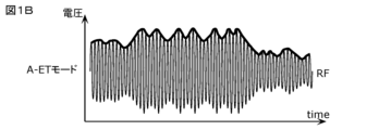
- Figure 1B is a graph showing an example of the change in power supply voltage in A-ET (Analog Envelope Tracking) mode.
- FIG. 1C is a graph showing an example of a transition of the power supply voltage in the D-ET mode.
- FIG. 2 is a circuit configuration diagram of the communication device according to the first embodiment.
- FIG. 3 is a circuit configuration diagram of a pre-regulator circuit, a switched capacitor circuit, and a power supply modulation circuit according to the first embodiment.
- FIG. 4 is a circuit configuration diagram of the envelope detection circuit, the control circuit, and the digital control circuit according to the first embodiment.
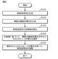
- FIG. 5 is a flowchart showing the amplification method according to the first embodiment.
- FIG. 6 is a component layout diagram of the communication device according to the first embodiment.
- FIG. 7 is a circuit configuration diagram of a communication device according to the second embodiment.
- FIG. 8 is a component layout diagram of a communication device according to the second embodiment.
- each figure is a schematic diagram in which emphasis, omissions, or adjustments to the ratio have been made as appropriate to illustrate the present invention, and is not necessarily an exact illustration, and may differ from the actual shape, positional relationship, and ratio.
- the same reference numerals are used for substantially the same configuration, and duplicate explanations may be omitted or simplified.
- the x-axis and y-axis are mutually orthogonal axes on a plane parallel to the main surface of the motherboard.
- the x-axis is parallel to a first side of the motherboard
- the y-axis is parallel to a second side of the motherboard that is orthogonal to the first side.
- the z-axis is an axis perpendicular to the main surface of the motherboard, with its positive direction indicating the upward direction and its negative direction indicating the downward direction.
- connection includes not only direct connection by a connection terminal and/or wiring conductor, but also electrical connection via other circuit elements.
- Directly connected means directly connected by a connection terminal and/or wiring conductor without going through other circuit elements.
- C is connected between A and B means that one end of C is connected to A and the other end of C is connected to B, meaning that C is arranged in series on the path connecting A and B.
- Path connecting A and B means a path made of a conductor that electrically connects A to B.
- terminal means the point where a conductor within an element terminates. Note that if the impedance of the conductor between elements is sufficiently low, a terminal is interpreted as any point on the conductor between elements or the entire conductor, not just a single point.
- FIG. 1A is a graph showing an example of the transition of the power supply voltage in APT mode.
- APT mode is a mode in which the power supply voltage is varied to multiple discrete voltage levels on a frame-by-frame basis based on the average power.
- a frame is a unit that makes up a high-frequency signal (modulated signal).
- a frame contains 10 subframes, each subframe contains multiple slots, and each slot is made up of multiple symbols.
- the subframe length is 1 ms, and the frame length is 10 ms.
- APT mode a mode in which the voltage level is varied in units of one frame or larger based on the average power
- a mode in which the voltage level is varied in units smaller than one frame e.g., subframe, slot, or symbol units.
- Figure 1B is a graph showing an example of the transition of the power supply voltage in A-ET mode.
- A-ET mode is a mode in which the power supply voltage is continuously varied based on an envelope signal.
- the power supply voltage can track the envelope of the modulating signal.
- the envelope signal is a signal that indicates the envelope of a modulated signal.
- the envelope value is expressed, for example, as the square root of (I 2 +Q 2 ).
- (I, Q) represents a constellation point.
- a constellation point is a point that represents a digitally modulated signal on a constellation diagram.
- (I, Q) is determined, for example, by a BBIC (Baseband Integrated Circuit) based on transmission information.
- BBIC Baseband Integrated Circuit
- Figure 1C is a graph showing an example of the transition of the power supply voltage in D-ET mode.
- D-ET mode is a mode in which the power supply voltage is varied to multiple discrete voltage levels within one frame based on an envelope signal.
- the power supply voltage can track the envelope of the modulating signal.
- the power supply voltage varies at shorter time intervals than in APT.
- the communication device 6 can be used to provide wireless connection.
- the communication device 6 can be implemented in a user terminal (UE: User Equipment) in a cellular network (also called a mobile network) such as a mobile phone, a smartphone, a tablet computer, or a wearable device.
- UE User Equipment
- a cellular network also called a mobile network
- the communication device 6 can be implemented to provide wireless connection to an Internet of Things (IoT) sensor device, a medical/healthcare device, a car, an unmanned aerial vehicle (UAV: Unmanned Aerial Vehicle) (so-called drone), or an automated guided vehicle (AGV: Automated Guided Vehicle).
- IoT Internet of Things
- UAV Unmanned Aerial Vehicle
- AGV Automated Guided Vehicle
- the communication device 6 can be implemented to provide wireless connection at a wireless access point or a wireless hotspot.
- FIG. 2 is an exemplary circuit configuration, and the communication device 6 may be implemented using any of a wide variety of circuit implementations and circuit technologies. Therefore, the description of the communication device 6 provided below should not be construed as limiting.
- the communication device 6 includes a tracker circuit 1, a power amplifier 2, a DC power supply 3, a transmission system 7 including an RFIC 4, and an antenna 5.
- the tracker circuit 1 can selectively supply at least one of a plurality of discrete voltages to the power amplifier 2. At this time, the tracker circuit 1 can select at least one voltage from a plurality of discrete voltages upon receiving a high-frequency signal generated by the RFIC 4. This allows the tracker circuit 1 to apply the D-ET mode to the power amplifier 2. The tracker circuit 1 may also be capable of applying the APT mode to the power amplifier 2. The circuit configuration of the tracker circuit 1 will be described later.
- the power amplifier 2 is an example of a first power amplifier, and is connected between the RFIC 4 and the antenna 5. Furthermore, the power amplifier 2 is connected to the tracker circuit 1.
- the power amplifier 2 can amplify the high-frequency signal supplied from the RFIC 4 using at least one of a plurality of discrete voltages selectively supplied from the tracker circuit 1.
- the DC power supply 3 can supply a DC voltage to the tracker circuit 1.
- the DC power supply 3 can be, for example, a rechargeable battery, but is not limited to this. Note that the DC power supply 3 does not have to be included in the transmission system 7, and does not have to be included in the communication device 6.
- the RFIC4 is an example of a signal processing circuit configured to generate a high-frequency signal (an example of a first high-frequency signal).
- the RFIC4 can generate a high-frequency signal by receiving a digital IQ signal, for example, from a BBIC (not shown), and performing digital-to-analog conversion, quadrature modulation, and up-conversion on the digital IQ signal.
- the RFIC4 may generate a digital control signal for controlling the tracker circuit 1. Note that some or all of the functions of the RFIC4 as a control unit may be implemented outside the RFIC4 (for example, in the tracker circuit 1).
- the antenna 5 can transmit the high-frequency signal amplified by the power amplifier 2 to the outside. Note that the antenna 5 does not have to be included in the communication device 6. Furthermore, the communication device 6 may further include one or more antennas in addition to the antenna 5.
- the circuit configuration of the communication device 6 shown in FIG. 2 is an example and is not limited to this.
- the communication device 6 may be equipped with a baseband signal processing circuit that processes signals using a frequency band lower than that of high-frequency signals.
- Figure 3 is a circuit configuration diagram of a pre-regulator circuit 10, a switched capacitor circuit 20, and a power supply modulation circuit 30 according to this embodiment.
- Figure 4 is a circuit configuration diagram of an envelope detection circuit 40, a switch control circuit 50, and a digital control circuit 60 according to this embodiment.
- Figures 2 to 4 are exemplary circuit configurations, and the tracker circuit 1, pre-regulator circuit 10, switched capacitor circuit 20, power supply modulation circuit 30, envelope detection circuit 40, switch control circuit 50, and digital control circuit 60 can be implemented using any of a wide variety of circuit implementations and circuit technologies. Therefore, the descriptions of the tracker circuit 1, pre-regulator circuit 10, switched capacitor circuit 20, power supply modulation circuit 30, envelope detection circuit 40, switch control circuit 50, and digital control circuit 60 provided below should not be interpreted as being limiting.
- the pre-regulator circuit 10 may also be called a magnetic regulator or a DC (Direct Current)/DC converter.
- the pre-regulator circuit 10 is a one-input, one-output buck-boost converter, and can convert the input voltage (Vbat) from the DC power supply 3 to an output voltage (regulated voltage).
- the pre-regulator circuit 10 may be a buck converter or a boost converter.
- the pre-regulator circuit 10 can change the output voltage based on a digital control signal from the RFIC 4, for example.
- the circuit configuration of the pre-regulator circuit 10 will be described later with reference to FIG. 3.
- the switched-capacitor circuit 20 can generate multiple discrete voltages based on the regulated voltage supplied from the pre-regulator circuit 10.
- the circuit configuration of the switched-capacitor circuit 20 will be described later with reference to FIG. 3.
- the voltage generation circuit 25 may not include the pre-regulator circuit 10 and/or the switched capacitor circuit 20.
- the pre-regulator circuit 10 may be disposed outside the voltage generation circuit 25, or even outside the tracker circuit 1.
- the voltage generation circuit 25 may include multiple pre-regulator circuits 10 without including the switched capacitor circuit 20.
- the envelope detection circuit 40 receives the high-frequency signal generated by the RFIC 4 and can detect the envelope of the high-frequency signal.
- the circuit configuration of the envelope detection circuit 40 will be described later with reference to FIG. 4.
- the switch control circuit 50 can generate control signals CS31 to CS33 (an example of a second control signal) for selecting at least one voltage from among a plurality of discrete voltages based on the envelope detected by the envelope detection circuit 40.
- the switch control circuit 50 can control the power supply modulation circuit 30 based on the high-frequency signal from the RFIC 4.
- the power supply modulation circuit 30 is not controlled based on a digital control signal from the RFIC 4.
- the circuit configuration of the switch control circuit 50 will be described later with reference to FIG. 4.
- the digital control circuit 60 can control the pre-regulator circuit 10 and the switched capacitor circuit 20 based on a digital control signal (an example of a first control signal) from the RFIC 4. Specifically, the digital control circuit 60 can generate and output a control signal for controlling the switches included in the pre-regulator circuit 10 and the switched capacitor circuit 20.
- the digital control circuit 60 will be described later with reference to FIG. 4. Note that the digital control circuit 60 does not have to be included in the tracker circuit 1.
- the external connection terminal 101 is an example of a first external connection terminal, and receives a control signal (first control signal) based on a serial data transmission standard.
- the external connection terminal 101 is externally connected to the RFIC 4, and internally connected to the digital control circuit 60.
- the control signal based on the serial data transmission standard may be, for example, a source synchronous or clock embedded control signal, but is not limited to these.
- the external connection terminal 102 is an example of a second external connection terminal, to which a high-frequency signal to be amplified by the power amplifier 2 is input.
- the external connection terminal 102 is externally connected to the RFIC 4 and internally connected to the envelope detection circuit 40.
- the external connection terminal 103 is an output terminal for supplying a power supply voltage to the power amplifier 2.
- the external connection terminal 103 is externally connected to the power amplifier 2 and internally connected to the power supply modulation circuit 30.
- the pre-regulator circuit 10 includes an input terminal T11, an output terminal T12, switches S11 to S14, a power inductor L11, and a capacitor C11.
- the input terminal T11 is a terminal for receiving a DC voltage (Vbat) from the DC power supply 3.
- the input terminal T11 is externally connected to the DC power supply 3 and internally connected to the switch S11.
- the output terminal T12 is a terminal for supplying an adjusted voltage to the switched capacitor circuit 20.
- the output terminal T12 is externally connected to the input terminal T21 of the switched capacitor circuit 20, and is internally connected to the switch S13.
- the power inductor L11 is an inductor used to step up and step down the DC voltage (Vbat). One end of the power inductor L11 is connected to the switches S11 and S12, and the other end of the power inductor L11 is connected to the switches S13 and S14.
- the switch S11 is connected between the input terminal T11 and one end of the power inductor L11. In this connection configuration, the switch S11 can switch between open and closed states to switch between connection and non-connection between the input terminal T11 and one end of the power inductor L11.
- the switch S12 is connected between one end of the power inductor L11 and the ground. In this connection configuration, the switch S12 can switch between opening and closing to switch between connection and disconnection between one end of the power inductor L11 and the ground.
- the switch S13 is connected between the other end of the power inductor L11 and the output terminal T12. In this connection configuration, the switch S13 can switch between open and closed states to connect and disconnect the other end of the power inductor L11 and the output terminal T12.
- the switch S14 is connected between the other end of the power inductor L11 and the ground. In this connection configuration, the switch S14 can be switched between open and closed to switch between connection and non-connection between the other end of the power inductor L11 and the ground.
- Capacitor C11 is connected between the path between switch S13 and output terminal T12 and ground. Specifically, one of the two electrodes of capacitor C11 is connected to switch S13 and output terminal T12, and the other of the two electrodes of capacitor C11 is connected to ground.
- the configuration of the pre-regulator circuit 10 shown in FIG. 3 is an example and is not limited to this.
- some of the switches S11 to S14 may be replaced with diodes.
- some or all of the pre-regulator circuit 10 may not be included in the tracker circuit 1.
- the switched capacitor circuit 20 has a ladder-type circuit configuration. Specifically, the switched capacitor circuit 20 includes capacitors C21 to C27, switches S21 to S2C, an input terminal T21, and output terminals T22 to T24. Energy and charge are input from the pre-regulator circuit 10 to node N3 via input terminal T21, and are extracted from nodes N1 to N3 to the power supply modulation circuit 30 via output terminals T22 to T24.
- the input terminal T21 is a terminal for receiving a regulated voltage from the pre-regulator circuit 10.
- the input terminal T21 is externally connected to the pre-regulator circuit 10 and internally connected to the node N3.
- Output terminal T22 is a terminal for supplying a voltage (V1) of the multiple discrete voltages to power supply modulation circuit 30.
- Output terminal T22 is externally connected to power supply modulation circuit 30 and internally connected to node N1.
- Output terminal T23 is a terminal for supplying a voltage (V2) of the multiple discrete voltages to power supply modulation circuit 30.
- Output terminal T23 is externally connected to power supply modulation circuit 30 and internally connected to node N2.
- the output terminal T24 is a terminal for supplying a voltage (V3) of the multiple discrete voltages to the power supply modulation circuit 30.
- the output terminal T24 is externally connected to the power supply modulation circuit 30 and internally connected to the node N3.
- the output terminal T24 may be integrated with the input terminal T21.
- VG represents the ground potential.
- One of the two electrodes of capacitor C21 is connected to one end of switch S21 and one end of switch S22.
- the other of the two electrodes of capacitor C21 is connected to one end of switch S25 and one end of switch S26.
- One of the two electrodes of capacitor C22 is connected to one end of switch S23 and one end of switch S24.
- the other of the two electrodes of capacitor C22 is connected to one end of switch S27 and one end of switch S28.
- One of the two electrodes of capacitor C23 is connected to one end of switch S25 and one end of switch S26.
- the other of the two electrodes of capacitor C23 is connected to one end of switch S29 and one end of switch S2A.
- One of the two electrodes of capacitor C24 is connected to one end of switch S27 and one end of switch S28.
- the other of the two electrodes of capacitor C24 is connected to one end of switch S2B and one end of switch S2C.
- Capacitors C25 to C27 are smoothing capacitors used to hold and smooth the voltages (V1 to V3) at nodes N1 to N3.
- Capacitor C25 is connected between nodes N2 and N3. Specifically, one of the two electrodes of capacitor C25 is connected to node N3. Meanwhile, the other of the two electrodes of capacitor C25 is connected to node N2.
- Capacitor C26 is connected between nodes N1 and N2. Specifically, one of the two electrodes of capacitor C26 is connected to node N2. Meanwhile, the other of the two electrodes of capacitor C26 is connected to node N1.
- Capacitor C27 is connected between node N1 and ground. Specifically, one of the two electrodes of capacitor C27 is connected to node N1. Meanwhile, the other of the two electrodes of capacitor C27 is connected to ground.
- the switch S21 is connected between the capacitor C21 and the node N2. Specifically, one end of the switch S21 is connected to one of the two electrodes of the capacitor C21. Meanwhile, the other end of the switch S21 is connected to the node N2.
- the switch S22 is connected between the capacitor C21 and the node N3. Specifically, one end of the switch S22 is connected to one of the two electrodes of the capacitor C21. Meanwhile, the other end of the switch S22 is connected to the node N3.
- Switch S23 is connected between capacitor C22 and node N2. Specifically, one end of switch S23 is connected to one of the two electrodes of capacitor C22. Meanwhile, the other end of switch S23 is connected to node N2.
- Switch S24 is connected between capacitor C22 and node N3. Specifically, one end of switch S24 is connected to one of the two electrodes of capacitor C22. Meanwhile, the other end of switch S24 is connected to node N3.
- Switch S25 is connected between capacitors C21 and C23 and node N1. Specifically, one end of switch S25 is connected to the other of the two electrodes of capacitor C21 and one of the two electrodes of capacitor C23. Meanwhile, the other end of switch S25 is connected to node N1.
- Switch S26 is connected between capacitors C21 and C23 and node N2. Specifically, one end of switch S26 is connected to the other of the two electrodes of capacitor C21 and one of the two electrodes of capacitor C23. Meanwhile, the other end of switch S26 is connected to node N2.
- Switch S27 is connected between capacitors C22 and C24 and node N1. Specifically, one end of switch S27 is connected to the other of the two electrodes of capacitor C22 and one of the two electrodes of capacitor C24. Meanwhile, the other end of switch S27 is connected to node N1.
- Switch S28 is connected between capacitors C22 and C24 and node N2. Specifically, one end of switch S28 is connected to the other of the two electrodes of capacitor C22 and one of the two electrodes of capacitor C24. Meanwhile, the other end of switch S28 is connected to node N2.
- Switch S29 is connected between capacitor C23 and ground. Specifically, one end of switch S29 is connected to the other of the two electrodes of capacitor C23. Meanwhile, the other end of switch S29 is connected to ground.
- Switch S2A is connected between capacitor C23 and node N1. Specifically, one end of switch S2A is connected to the other of the two electrodes of capacitor C23. Meanwhile, the other end of switch S2A is connected to node N1.
- Switch S2B is connected between capacitor C24 and ground. Specifically, one end of switch S2B is connected to the other of the two electrodes of capacitor C24. Meanwhile, the other end of switch S2B is connected to ground.
- Switch S2C is connected between capacitor C24 and node N1. Specifically, one end of switch S2C is connected to the other of the two electrodes of capacitor C24. Meanwhile, the other end of switch S2C is connected to node N1.
- the first set of switches including switches S22, S23, S26, S27, S2A, and S2B and the second set of switches including switches S21, S24, S25, S28, S29, and S2C are switched between open and closed inversely based on a control signal CS20 from the digital control circuit 60.
- the first set of switches are closed and the second set of switches are opened.
- one of the two electrodes of capacitor C21 is connected to node N3, the other of the two electrodes of capacitor C21, one of the two electrodes of capacitor C22, and one of the two electrodes of capacitor C23 are connected to node N2, the other of the two electrodes of capacitor C22, the other of the two electrodes of capacitor C23, and one of the two electrodes of capacitor C24 are connected to node N3, and the other of the two electrodes of capacitor C24 is connected to ground.
- the first set of switches is opened and the second set of switches is closed.
- one of the two electrodes of capacitor C22 is connected to node N3
- one of the two electrodes of capacitor C21, the other of the two electrodes of capacitor C22, and one of the two electrodes of capacitor C24 are connected to node N2
- the other of the two electrodes of capacitor C21, one of the two electrodes of capacitor C23, and the other of the two electrodes of capacitor C24 are connected to node N3, and the other of the two electrodes of capacitor C23 is connected to ground.
- the capacitors C21 to C24 can be charged and discharged in a complementary manner. For example, in one of the first and second phases, charging of the capacitors C25 to C27 is performed from the capacitors C21 and C23, and in the other of the first and second phases, charging of the capacitors C25 to C27 is performed from the capacitors C22 and C24.
- the capacitors C25 to C27 are always charged from one of the capacitors C21 to C24, even if a current flows from the node N1, N2, or N3 to the power supply modulation circuit 30 at high speed, the charge is replenished at the node N1, N2, or N3 at high speed, and the potential fluctuation of the node N1, N2, or N3 can be suppressed.
- V3-V2):(V2-V1):(V1-VG) is not limited to 1:1:1, and can be designed to any ratio (e.g., 1:2:3, 1:2:4, 3:2:1, 4:2:1, etc.).
- the power supply modulation circuit 30 has input terminals T31 to T33, switches S31 to S33, and an output terminal T34.
- the input terminals T31 to T33 are terminals for receiving a plurality of discrete voltages (V1 to V3) generated by the switched capacitor circuit 20.
- the input terminals T31 to T33 are externally connected to the output terminals T22 to T24 of the switched capacitor circuit 20, respectively, and internally connected to the switches S31 to S33, respectively.
- Output terminal T34 is a terminal for selectively supplying at least one of a plurality of discrete voltages to power amplifier 2.
- Output terminal T34 is externally connected to power amplifier 2 and internally connected to switches S31 to S33.
- the switch S31 is connected between the input terminal T31 and the output terminal T34.
- the switch S31 can be switched between open and closed by a control signal CS31 from the switch control circuit 50, thereby switching between connection and non-connection between the input terminal T31 and the output terminal T34.
- the switch S32 is connected between the input terminal T32 and the output terminal T34.
- the switch S32 can be switched between open and closed by a control signal CS32 from the switch control circuit 50, thereby switching between connection and non-connection between the input terminal T32 and the output terminal T34.
- the switch S33 is connected between the input terminal T33 and the output terminal T34.
- the switch S33 can be switched between open and closed by a control signal CS33 from the switch control circuit 50, thereby switching between connection and non-connection between the input terminal T33 and the output terminal T34.
- these switches S31 to S33 are controlled to be exclusively on. In other words, only one of the switches S31 to S33 is closed, and all the remaining switches S31 to S33 are controlled to be open. This allows the power supply modulation circuit 30 to supply one voltage selected from a plurality of discrete voltages (V1 to V3) to the power amplifier 2.
- the configuration of the power supply modulation circuit 30 shown in FIG. 3 is an example and is not limited to this.
- the switches S31 to S33 may have any configuration and may be controlled in any manner as long as they can selectively connect at least one of the three input terminals T31 to T33 to the output terminal T34. For example, two of the switches S31 to S33 may be closed and the remaining one of the switches S31 to S33 may be open.
- the envelope detection circuit 40 includes an input terminal T41, an output terminal T42, a diode D41, a capacitor C41, and a resistor R41.
- the input terminal T41 is a terminal for receiving a high-frequency signal.
- the input terminal T41 is externally connected to the external connection terminal 102 and internally connected to the input end of the diode D41.
- the output terminal T42 is a terminal for supplying an envelope signal to the switch control circuit 50.
- the output terminal T42 is externally connected to the switch control circuit 50 and internally connected to the output terminal of the diode D41.
- Diode D41 is connected between input terminal T41 and output terminal T42.
- Capacitor C41 is connected in parallel with resistor R41 between the path between the output end of diode D41 and output terminal T42 and ground.
- Resistor R41 is connected in parallel with capacitor C41 between the path between the output end of diode D41 and output terminal T42 and ground.
- FIG. 4 illustrates the simplest circuit configuration of the envelope detection circuit 40
- the circuit configuration of the envelope detection circuit 40 is not limited to this.
- the switch control circuit 50 includes an input terminal T51, output terminals T52 to T54, and comparators C51 to C54.
- the input terminal T51 is a terminal for receiving an envelope signal.
- the input terminal T51 is externally connected to the envelope detection circuit 40 and internally connected to the comparators C51 to C54.
- Output terminals T52 to T54 are terminals for supplying control signals CS31 to CS33, respectively, to the power supply modulation circuit 30.
- the output terminals T52 to T54 are connected to the power supply modulation circuit 30.
- the control signals CS31 to CS33 are an example of a second control signal, and are signals for selecting at least one voltage from among a plurality of discrete voltages. Specifically, the control signals CS31 to CS33 are signals for controlling the opening and closing of the switches S31 to S33 of the power supply modulation circuit 30, respectively.
- the switch S31 when the control signal CS31 has a high level voltage, the switch S31 is closed, and when the control signal CS31 has a low level voltage, the switch S31 is opened.
- the control signal CS32 has a high level voltage
- the switch S32 is closed, and when the control signal CS32 has a low level voltage, the switch S32 is opened.
- the control signal CS33 has a high level voltage
- the switch S33 is closed, and when the control signal CS33 has a low level voltage, the switch S33 is opened.
- the relationship between the voltages of the control signals CS31 to CS33 and the opening and closing of the switches S31 to S33 may be reversed.
- the switches may be opened when the control signals have a high-level voltage, and closed when the control signals have a low-level voltage.
- Comparator C51 can compare the envelope signal with reference voltage Vref1.
- the non-inverting input terminal of comparator C51 is connected to a voltage source of reference voltage Vref1.
- the inverting input terminal of comparator C51 is connected to input terminal T51.
- the output terminal of comparator C51 is connected to output terminal T52.
- Comparator C52 can compare the envelope signal with a reference voltage Vref1.
- the non-inverting input terminal of comparator C52 is connected to input terminal T51.
- the inverting input terminal of comparator C52 is connected to the voltage source of Vref1.
- the output terminal of comparator C52 is connected to output terminal T53.
- Comparator C53 can compare the envelope signal with reference voltage Vref2.
- the non-inverting input terminal of comparator C53 is connected to a voltage source of reference voltage Vref2.
- the inverting input terminal of comparator C53 is connected to input terminal T51.
- the output terminal of comparator C53 is connected to output terminal T53. Note that reference voltage Vref2 is higher than reference voltage Vref1.
- Comparators C52 and C53 form a window comparator circuit.
- the window comparator circuit outputs a high-level voltage to output terminal T53 when the envelope signal is within the range of reference voltages Vref1 and Vref2, and outputs a low-level voltage to output terminal T53 when the envelope signal is not within the range of reference voltages Vref1 and Vref2.
- Comparator C54 can compare the envelope signal with reference voltage Vref2.
- the non-inverting input terminal of comparator C54 is connected to input terminal T51.
- the inverting input terminal of comparator C54 is connected to the voltage source of reference voltage Vref2.
- the output terminal of comparator C54 is connected to output terminal T54. This allows comparator C54 to output a high-level voltage to output terminal T54 when the envelope signal is higher than reference voltage Vref2, and to output a low-level voltage to output terminal T54 when the envelope signal is lower than reference voltage Vref2.
- the switch control circuit 50 can generate a control signal CS31 for selecting a first voltage (V1) from among a plurality of discrete voltages when the envelope signal is lower than the reference voltage Vref1.
- the switch control circuit 50 can also generate a control signal CS32 for selecting a second voltage (V2) from among a plurality of discrete voltages when the envelope signal is higher than the reference voltage Vref1 and lower than the reference voltage Vref2.
- the switch control circuit 50 can also generate a control signal CS33 for selecting a third voltage (V3) from among a plurality of discrete voltages when the envelope signal is higher than the reference voltage Vref2.
- the circuit configuration of the switch control circuit 50 shown in FIG. 4 is an example and is not limited to this.
- the switch control circuit 50 may be configured to output a digital control line (DCL) signal to the digital control circuit 60 instead of the control signals CS31 to CS33.
- the digital control circuit 60 may generate the control signals CS31 to CS33 for the switches S31 to S33 from the DCL signal.
- the digital control circuit 60 can receive a digital control signal (an example of a first control signal) based on the serial data transmission standard via the external connection terminal 101.
- a source synchronous digital control signal is used as the digital control signal based on the serial data transmission standard. Therefore, the digital control circuit 60 can receive a clock signal (CLK) and a data signal (DATA) via each of the two external connection terminals 101.
- the digital control circuit 60 processes a clock signal (CLK) and a data signal (DATA) to generate control signals CS10 and CS20 for controlling the pre-regulator circuit 10 and the switched capacitor circuit 20, respectively.
- CLK clock signal
- DATA data signal
- the opening and closing of the switches S11 to S14 included in the pre-regulator circuit 10 is controlled by the control signal CS10, and the switches S21 to S2C included in the switched capacitor circuit 20 are controlled by the control signal CS20.
- Fig. 5 is a flow chart showing the amplification method according to the present embodiment.
- the RFIC 4 generates a high-frequency signal (S101).
- the pre-regulator circuit 10 and the switched capacitor circuit 20 generate a plurality of discrete voltages (V1 to V3) (S102).
- the envelope detection circuit 40 detects the envelope of the high-frequency signal generated by the RFIC 4 (S103).
- the power supply modulation circuit 30 selects at least one voltage from the plurality of discrete voltages (V1 to V3) based on the envelope detected by the envelope detection circuit 40 (S104).
- the power amplifier 2 amplifies the high-frequency signal generated by the RFIC 4 using the at least one selected voltage (S105).
- Fig. 6 is a component layout diagram of the communication device 6 according to the present embodiment.
- each component is given an abbreviation (such as "ANT") indicating its function so that the layout relationship of each component can be easily understood, but the actual components do not need to be given such an abbreviation.
- abbreviation such as "ANT"
- conductors electrically connecting the components are represented by simple lines.
- the motherboard 8 is equipped with a tracker module (DET), a PA module (PA1), and an RFIC 4.
- DET tracker module
- PA1 PA module
- RFIC 4 RFIC 4.
- the tracker module (DET) is equipped with a tracker circuit 1.
- the tracker module (DET) is disposed adjacent to the PA module (PA1) in a plan view of the motherboard 8.
- the external connection terminal 101 of the tracker module (DET) is connected to the RFIC 4, and a clock signal (CLK) and a data signal (DATA) are supplied from the RFIC 4.
- the external connection terminal 102 of the tracker module (DET) is connected to the RFIC 4, and a radio frequency signal (RF) is supplied from the RFIC 4.
- RF radio frequency signal
- the conductor connecting the RFIC 4 and the tracker module (DET) branches off from the conductor connecting the RFIC 4 and the PA module (PA1).
- the external connection terminal 103 of the tracker module (DET) is connected to the PA module (PA1), and supplies a power supply voltage (Vcc).
- the PA module (PA1) is equipped with a power amplifier 2.
- the PA module (PA1) is disposed near the antenna 5.
- the antenna 5 is located on the upper side of the motherboard 8, near the PA module (PA1).
- the transmission system 7 of this embodiment includes an RFIC 4 configured to generate a first high-frequency signal, a power amplifier 2 configured to amplify the first high-frequency signal, and a tracker circuit 1 configured to selectively supply at least one of a plurality of discrete voltages to the power amplifier 2, and the tracker circuit 1 is configured to receive the first high-frequency signal generated by the RFIC 4 and select at least one voltage from the plurality of discrete voltages.
- At least one voltage is selected from among a plurality of discrete voltages upon receiving a high-frequency signal, so the RFIC 4 does not need to generate a digital control signal for voltage selection.
- the voltage needs to be switched quickly based on the envelope, so it is difficult to control the voltage selection with a digital control signal based on a normal serial data transmission standard.
- a digital control signal e.g., a digital control level signal
- a circuit that generates a digital control signal based on the parallel data transmission standard needs to be incorporated into the RFIC 4.
- the tracker circuit 1 receives a high-frequency signal and selects a voltage, so a circuit that generates a digital control signal based on the parallel data transmission standard does not need to be incorporated into the RFIC 4, and D-ET can be realized with a simple RFIC 4.
- the tracker circuit 1 may include an envelope detection circuit 40 configured to receive the first high-frequency signal generated by the RFIC 4 and detect the envelope of the first high-frequency signal, and a switch control circuit 50 configured to generate a control signal for selecting at least one voltage from among a plurality of discrete voltages based on the envelope detected by the envelope detection circuit 40.
- the multiple discrete voltages may include a first voltage and a second voltage higher than the first voltage
- the switch control circuit 50 may be configured to generate a control signal for selecting the first voltage from among the multiple discrete voltages when the envelope is lower than the reference voltage, and may be configured to generate a control signal for selecting the second voltage from among the multiple discrete voltages when the envelope is higher than the reference voltage.
- the switch control circuit 50 may be configured to generate a digital control level signal as the control signal.
- the tracker circuit 1 includes a voltage generation circuit 25 configured to generate a plurality of discrete voltages, a power supply modulation circuit 30 configured to selectively output at least one of the plurality of discrete voltages to the power amplifier 2, an external connection terminal 101 to which a first control signal (CLK, DATA) based on the serial data transmission standard is input, and an external connection terminal 102 to which a high-frequency signal to be amplified by the power amplifier 2 is input, and the voltage generation circuit 25 is controlled based on the first control signal, and the power supply modulation circuit 30 is controlled based on the high-frequency signal.
- CLK, DATA first control signal
- the power supply modulation circuit 30 is controlled based on the high frequency signal, so the tracker circuit 1 does not need to receive a digital control signal for voltage selection from the RFIC 4. Therefore, a circuit for generating a digital control signal based on the parallel data transmission standard does not need to be incorporated into the RFIC 4, and D-ET can be realized with a simple RFIC 4.
- the tracker circuit 1 may further include an envelope detection circuit 40 configured to detect the envelope of the high-frequency signal input via the external connection terminal 102, and a switch control circuit 50 configured to generate a second control signal (CS31 to CS33) for selecting at least one voltage from among a plurality of discrete voltages based on the envelope detected by the envelope detection circuit 40.
- an envelope detection circuit 40 configured to detect the envelope of the high-frequency signal input via the external connection terminal 102
- a switch control circuit 50 configured to generate a second control signal (CS31 to CS33) for selecting at least one voltage from among a plurality of discrete voltages based on the envelope detected by the envelope detection circuit 40.
- the switch control circuit 50 may include comparators C51 to C54 that compare the envelope with a reference voltage.
- switch control circuit 50 This allows the switch control circuit 50 to be configured using relatively simple circuits such as comparators C51 to C54.
- the switch control circuit 50 may be configured to generate a digital control level signal as the second control signal.
- the amplification method also generates a high-frequency signal (S101), generates a plurality of discrete voltages (S102), detects the envelope of the generated high-frequency signal (S103), selects at least one voltage from the generated plurality of discrete voltages based on the detected envelope (S104), and amplifies the high-frequency signal using the selected at least one voltage (S105).
- S101 high-frequency signal
- S102 generates a plurality of discrete voltages
- S103 detects the envelope of the generated high-frequency signal
- S104 selects at least one voltage from the generated plurality of discrete voltages based on the detected envelope
- S105 selected at least one voltage
- the communication device includes a power amplifier to which the APT mode is applied and to which the D-ET mode is not applied.
- Fig. 7 is a circuit configuration diagram of the communication device 6A according to this embodiment.
- FIG. 7 is an exemplary circuit configuration, and the communication device 6A may be implemented using any of a wide variety of circuit implementations and circuit technologies. Therefore, the description of the communication device 6A provided below should not be construed as limiting.
- the communication device 6A includes a transmission system 7A and an antenna 5.
- the transmission system 7A includes a tracker circuit 1, a power amplifier 2, a DC power supply 3, an RFIC 4A, a DC/DC converter circuit 10A, and a power amplifier 2A.
- the RFIC 4A can generate a second high-frequency signal that is supplied to the power amplifier 2A in addition to the first high-frequency signal that is supplied to the power amplifier 2.
- the DC/DC converter circuit 10A can convert the input voltage (Vbat) from the DC power supply 3 into a supply voltage (Vcc) to the power amplifier 2A.
- the DC/DC converter circuit 10A can change the supply voltage (Vcc) to the power amplifier 2A based on the average power of the second high-frequency signal supplied to the power amplifier 2A. This allows the DC/DC converter circuit 10A to apply the APT mode to the power amplifier 2A.
- the DC/DC converter circuit 10A has a circuit configuration similar to that of the pre-regulator circuit 10, so illustration and description thereof will be omitted.
- the power amplifier 2A is connected between the RFIC 4A and the antenna 5. Furthermore, the power amplifier 2A is connected to a DC/DC converter circuit 10A. The power amplifier 2A can amplify the second high frequency signal supplied from the RFIC 4A using the voltage supplied from the DC/DC converter circuit 10A.
- Fig. 8 is a component layout diagram of the communication device 6A according to this embodiment.
- each component is given an abbreviation (such as "ANT") indicating its function so that the layout relationship of each component can be easily understood, but the actual components do not need to be given such an abbreviation.
- abbreviation such as "ANT"
- conductors electrically connecting the components are represented by simple lines.
- the motherboard 8 is equipped with a tracker module (DET), PA modules (PA1, PA2), an RFIC 4A, and a converter module (DC/DC).
- DET tracker module
- PA modules PA1, PA2
- RFIC 4A RFIC 4A
- DC/DC converter module
- the converter module (DC/DC) is equipped with a DC/DC converter circuit 10A.
- the converter module (DC/DC) is disposed adjacent to the PA module (PA2) in a plan view of the motherboard 8.
- the PA module (PA2) is equipped with a power amplifier 2A.
- the PA module (PA2) is disposed near the antenna 5.
- the RFIC 4A may be further configured to generate a second high-frequency signal
- the transmission system 7A may further include a DC/DC converter circuit 10A configured to convert an input voltage into a supply voltage, and a power amplifier 2A configured to amplify the second high-frequency signal using the supply voltage from the DC/DC converter circuit 10A.
- the transmission system, tracker circuit, and amplification method according to the present invention have been described above based on the embodiments, the transmission system, tracker circuit, and amplification method according to the present invention are not limited to the above-mentioned embodiments.
- the present invention also includes other embodiments realized by combining any of the components in the above-mentioned embodiments, modifications obtained by applying various modifications to the above-mentioned embodiments that would come to mind by a person skilled in the art without departing from the spirit of the present invention, and various devices incorporating the above-mentioned transmission system or the above-mentioned tracker circuit.
- circuit elements and wiring may be inserted between the paths connecting the circuit elements and signal paths disclosed in the drawings.
- a filter and/or an impedance matching circuit may be inserted between the power amplifier 2 and the antenna 5.
- the tracker circuit 1 may supply voltage to multiple power amplifiers.
- the tracker circuit 1 may include multiple power modulation circuits 30.
- a signal processing circuit configured to generate a first high frequency signal; a first power amplifier configured to amplify the first radio frequency signal; a tracker circuit configured to selectively supply at least one of a plurality of discrete voltages to the first power amplifier; the tracker circuit is configured to receive the first high frequency signal generated by the signal processing circuit and select at least one voltage from among the plurality of discrete voltages. Transmission system.
- the tracker circuit includes: an envelope detection circuit configured to receive the first high frequency signal generated by the signal processing circuit and detect an envelope of the first high frequency signal; and a switch control circuit configured to generate a control signal for selecting at least one voltage from among the plurality of discrete voltages based on the envelope detected by the envelope detection circuit.
- the plurality of discrete voltages includes a first voltage and a second voltage higher than the first voltage;
- the switch control circuit includes: configured to generate a control signal for selecting the first voltage from among the plurality of discrete voltages when the envelope is lower than a reference voltage; and configured to generate a control signal for selecting the second voltage from among the plurality of discrete voltages when the envelope is higher than the reference voltage.
- the switch control circuit is configured to generate a digital control level signal as the control signal.
- the signal processing circuit is further configured to generate a second high frequency signal;
- the transmission system further comprises: a converter circuit configured to convert an input voltage to a supply voltage; a second power amplifier configured to amplify the second high frequency signal using the supply voltage from the converter circuit.
- a transmission system according to any one of ⁇ 1> to ⁇ 4>.
- a voltage generating circuit configured to generate a plurality of discrete voltages; a power supply modulation circuit configured to selectively output at least one of the plurality of discrete voltages to a power amplifier; a first external connection terminal to which a first control signal based on a serial data transmission standard is input; a second external connection terminal to which a high-frequency signal amplified by the power amplifier is input; the voltage generating circuit is controlled based on the first control signal; The power supply modulation circuit is controlled based on the high frequency signal. Tracker circuit.
- the tracker circuit further comprises: an envelope detection circuit configured to detect an envelope of the high frequency signal input via the second external connection terminal; and a switch control circuit configured to generate a second control signal for selecting at least one voltage from among the plurality of discrete voltages based on the envelope detected by the envelope detection circuit.
- the tracker circuit according to ⁇ 6>.
- the switch control circuit includes a comparator that compares the envelope with a reference voltage.
- the tracker circuit according to ⁇ 7>.
- the switch control circuit is configured to generate a digital control level signal as the second control signal.
- the tracker circuit according to ⁇ 7> or ⁇ 8>.
- ⁇ 10> Generates a high frequency signal, generating a plurality of discrete voltages; Detecting an envelope of the generated high frequency signal; selecting at least one voltage from among the generated plurality of discrete voltages based on the detected envelope; amplifying the radio frequency signal using the at least one selected voltage; Amplification methods.
- the present invention can be widely used as a transmission system for transmitting high-frequency signals in communication devices such as mobile phones.
- Tracker circuit 2 2A Power amplifier 3 DC power supply 4, 4A RFIC 5 Antenna 6, 6A Communication device 7, 7A Transmission system 8 Motherboard 10 Pre-regulator circuit 10A DC/DC converter circuit 20 Switched capacitor circuit 25 Voltage generation circuit 30 Power supply modulation circuit 40 Envelope detection circuit 50 Switch control circuit 60 Digital control circuit 101, 102, 103 External connection terminal
Landscapes
- Engineering & Computer Science (AREA)
- Power Engineering (AREA)
- Computer Networks & Wireless Communication (AREA)
- Signal Processing (AREA)
- Physics & Mathematics (AREA)
- Electromagnetism (AREA)
- General Physics & Mathematics (AREA)
- Radar, Positioning & Navigation (AREA)
- Automation & Control Theory (AREA)
- Amplifiers (AREA)
Abstract
送信システム(7)は、第1高周波信号を生成するよう構成されたRFIC(4)と、第1高周波信号を増幅するよう構成された電力増幅器(2)と、複数の離散的電圧のうちの少なくとも1つを選択的に電力増幅器(2)に供給するよう構成されたトラッカ回路(1)と、を備え、トラッカ回路(1)は、RFIC(4)によって生成された第1高周波信号を受けて複数の離散的電圧の中から少なくとも1つの電圧を選択するよう構成されている。
Description
本発明は、送信システム、トラッカ回路及び増幅方法に関する。
特許文献1は、平均出力電力に応じて電力増幅器の電源電圧を制御することによって電力効率の向上を図る平均電力トラッキング(APT:Average Power Tracking)を開示している。特許文献2は、さらなる電力付加効率の改善のためのデジタル・エンベロープ・トラッキング(D-ET:Digital Envelope Tracking)を開示している。
しかしながら、特許文献2に開示された送信システムでは、電圧選択のための制御信号を生成する回路がRFIC(Radio Frequency Integrated Circuit)に組み込まれる必要があり、特許文献1に開示されたAPTのためのRFICではD-ETを実現することが難しい。
そこで、本発明は、簡素なRFICでD-ETを実現することができる送信システム、トラッカ回路、及び、増幅方法を提供する。
本発明の一態様に係る送信システムは、第1高周波信号を生成するよう構成された信号処理回路と、第1高周波信号を増幅するよう構成された第1電力増幅器と、複数の離散的電圧のうちの少なくとも1つを選択的に第1電力増幅器に供給するよう構成されたトラッカ回路と、を備え、トラッカ回路は、信号処理回路によって生成された第1高周波信号を受けて複数の離散的電圧の中から少なくとも1つの電圧を選択するよう構成されている。
本発明の一態様に係るトラッカ回路は、複数の離散的電圧を生成するよう構成された電圧生成回路と、複数の離散的電圧のうちの少なくとも1つを選択的に電力増幅器に出力するよう構成された電源変調回路と、シリアルデータ伝送規格に基づく第1制御信号が入力される第1外部接続端子と、電力増幅器で増幅される高周波信号が入力される第2外部接続端子と、を備え、電圧生成回路は、第1制御信号に基づいて制御され、電源変調回路は、高周波信号に基づいて制御される。
本発明の一態様に係る増幅方法は、高周波信号を生成し、複数の離散的電圧を生成し、生成された高周波信号の包絡線を検出し、検出された包絡線に基づいて、生成された複数の離散的電圧の中から少なくとも1つの電圧を選択し、選択された少なくとも1つの電圧を用いて、高周波信号を増幅する。
本発明によれば、簡素なRFICでD-ETを実現することができる。
以下、本発明の実施の形態について、図面を用いて詳細に説明する。なお、以下で説明する実施の形態は、いずれも包括的又は具体的な例を示すものである。以下の実施の形態で示される数値、形状、材料、構成要素、構成要素の配置及び接続形態などは、一例であり、本発明を限定する主旨ではない。
なお、各図は、本発明を示すために適宜強調、省略、又は比率の調整を行った模式図であり、必ずしも厳密に図示されたものではなく、実際の形状、位置関係、及び比率とは異なる場合がある。各図において、実質的に同一の構成に対しては同一の符号を付しており、重複する説明は省略又は簡素化される場合がある。
以下の各図において、x軸及びy軸は、マザー基板の主面と平行な平面上で互いに直交する軸である。具体的には、平面視においてマザー基板が矩形状を有する場合、x軸は、マザー基板の第1辺に平行であり、y軸は、マザー基板の第1辺と直交する第2辺に平行である。また、z軸は、マザー基板の主面に垂直な軸であり、その正方向は上方向を示し、その負方向は下方向を示す。
以下の説明において、「接続される」とは、接続端子及び/又は配線導体で直接接続される場合だけでなく、他の回路素子を介して電気的に接続される場合も含む。「直接接続される」とは、他の回路素子を介さずに接続端子及び/又は配線導体で直接接続されることを意味する。「CがA及びBの間に接続される」とは、Cの一端がAに接続され、Cの他端がBに接続されることを意味し、A及びBの間を結ぶ経路にCが直列配置されることを意味する。「A及びBの間を結ぶ経路」とは、AをBに電気的に接続する導体で構成された経路を意味する。
以下の説明において、「端子」とは、要素内の導体が終了するポイントを意味する。なお、要素間の導体のインピーダンスが十分に低い場合には、端子は、単一のポイントだけでなく、要素間の導体上の任意のポイント又は導体全体と解釈される。
また、「平行」及び「垂直」などの要素間の関係性を示す用語、及び、「矩形」などの要素の形状を示す用語、並びに、数値範囲は、厳格な意味のみを表すのではなく、実質的に同等な範囲、例えば数%程度の誤差をも含むことを意味する。
まず、高周波信号を高効率に増幅する技術として、高周波信号に基づいて時間の経過とともに動的に調整された電源電圧を電力増幅器に供給するトラッキングモードについて説明する。トラッキングモードとは、電力増幅器に印加される電源電圧を動的に調整するモードである。トラッキングモードにはいくつかの種類があるが、ここでは、APTモード、A-ETモード及びD-ETモードについて図1A~図1Cを参照しながら説明する。図1A~図1Cにおいて、横軸は時間を表し、縦軸は電圧を表す。また、太い実線は、電源電圧を表し、細い実線(波形)は、変調信号を表す。
図1Aは、APTモードにおける電源電圧の推移の一例を示すグラフである。APTモードとは、平均パワーに基づいて、1フレーム単位で複数の離散的な電圧レベルに電源電圧を変動させるモードである。
フレームとは、高周波信号(変調信号)を構成する単位を意味する。例えば5GNR(5th Generation New Radio)及びLTE(Long Term Evolution)では、フレームは、10個のサブフレームを含み、各サブフレームは、複数のスロットを含み、各スロットは、複数のシンボルで構成される。サブフレーム長は1msであり、フレーム長は10msである。
なお、平均パワーに基づいて1フレーム単位又はそれよりも大きな単位で電圧レベルを変動させるモードをAPTモードと呼び、1フレームよりも小さな単位(例えばサブフレーム、スロット又はシンボル単位)で電圧レベルを変動させるモードと区別する。
図1Bは、A-ETモードにおける電源電圧の推移の一例を示すグラフである。A-ETモードとは、エンベロープ信号に基づいて電源電圧を連続的に変動させるモードである。A-ETモードでは、電源電圧が変調信号の包絡線を追跡することができる。
エンベロープ信号とは、変調信号の包絡線を示す信号である。エンベロープ値は、例えば(I2+Q2)の平方根で表される。ここで、(I,Q)は、コンスタレーションポイントを表す。コンスタレーションポイントとは、デジタル変調された信号をコンスタレーションダイヤグラム上で表す点である。(I,Q)は、例えば、送信情報に基づいてBBIC(Baseband Integrated Circuit)で決定される。
図1Cは、D-ETモードにおける電源電圧の推移の一例を示すグラフである。D-ETモードとは、エンベロープ信号に基づいて、1フレーム内で複数の離散的な電圧レベルに電源電圧を変動させるモードである。D-ETモードでは、電源電圧が変調信号の包絡線を追跡することができる。D-ETでは、APTよりも短い時間間隔で電源電圧が変動する。
(実施の形態1)
以下に、実施の形態1について説明する。本実施の形態に係る通信装置6は、無線接続を提供するために使用することができる。例えば、携帯電話、スマートフォン、タブレットコンピュータ、ウェアラブル・デバイスなどのセルラーネットワーク(モバイルネットワークともいう)におけるユーザ端末(UE:User Equipment)に通信装置6を実装することができる。別の例では、通信装置6を実装することで、IoT(Internet of Things)センサ・デバイス、医療/ヘルスケア・デバイス、車、無人航空機(UAV:Unmanned Aerial Vehicle)(いわゆるドローン)、無人搬送車(AGV:Automated Guided Vehicle)に無線接続を提供することができる。さらに別の例では、通信装置6を実装することで、無線アクセスポイント又は無線ホットスポットで無線接続を提供することもできる。
以下に、実施の形態1について説明する。本実施の形態に係る通信装置6は、無線接続を提供するために使用することができる。例えば、携帯電話、スマートフォン、タブレットコンピュータ、ウェアラブル・デバイスなどのセルラーネットワーク(モバイルネットワークともいう)におけるユーザ端末(UE:User Equipment)に通信装置6を実装することができる。別の例では、通信装置6を実装することで、IoT(Internet of Things)センサ・デバイス、医療/ヘルスケア・デバイス、車、無人航空機(UAV:Unmanned Aerial Vehicle)(いわゆるドローン)、無人搬送車(AGV:Automated Guided Vehicle)に無線接続を提供することができる。さらに別の例では、通信装置6を実装することで、無線アクセスポイント又は無線ホットスポットで無線接続を提供することもできる。
[1.1 通信装置6の回路構成]
本実施の形態に係る通信装置6の回路構成について、図2を参照しながら説明する。図2は、本実施の形態に係る通信装置6の回路構成図である。
本実施の形態に係る通信装置6の回路構成について、図2を参照しながら説明する。図2は、本実施の形態に係る通信装置6の回路構成図である。
なお、図2は、例示的な回路構成であり、通信装置6は、多種多様な回路実装及び回路技術のいずれかを使用して実装され得る。したがって、以下に提供される通信装置6の説明は、限定的に解釈されるべきではない。
本実施の形態に係る通信装置6は、トラッカ回路1、電力増幅器2、直流電源3、及び、RFIC4を含む送信システム7と、アンテナ5と、を備える。
トラッカ回路1は、複数の離散的電圧のうちの少なくとも1つを選択的に電力増幅器2に供給することができる。このとき、トラッカ回路1は、RFIC4で生成された高周波信号を受けて複数の離散的電圧の中から少なくとも1つの電圧を選択することができる。これにより、トラッカ回路1は、電力増幅器2にD-ETモードを適用することができる。また、トラッカ回路1は、電力増幅器2にAPTモードを適用可能であってもよい。トラッカ回路1の回路構成については後述する。
電力増幅器2は、第1電力増幅器の一例であり、RFIC4とアンテナ5との間に接続される。さらに、電力増幅器2は、トラッカ回路1に接続される。電力増幅器2は、トラッカ回路1から選択的に供給された複数の離散的電圧のうちの少なくとも1つを用いて、RFIC4から供給された高周波信号を増幅することができる。
直流電源3は、トラッカ回路1に直流電圧を供給することができる。直流電源3としては、例えば、充電式電池(rechargeable battery)を用いることができるが、これに限定されない。なお、直流電源3は、送信システム7に含まれなくてもよく、通信装置6に含まれなくてもよい。
RFIC4は、高周波信号(第1高周波信号の一例)を生成するよう構成された信号処理回路の一例である。RFIC4は、例えばBBIC(図示せず)からデジタルIQ信号を受け、デジタルIQ信号にデジタル・アナログ変換、直交変調、及び、アップコンバートなどを行うことにより、高周波信号を生成することができる。さらに、RFIC4は、トラッカ回路1を制御するためのデジタル制御信号を生成してもよい。なお、RFIC4の制御部としての機能の一部又は全部は、RFIC4の外部(例えばトラッカ回路1など)に実装されてもよい。
アンテナ5は、電力増幅器2で増幅された高周波信号を外部に送信することができる。なお、アンテナ5は、通信装置6に含まれなくてもよい。また、通信装置6は、アンテナ5に加えて、さらに1以上のアンテナを備えてもよい。
なお、図2に表された通信装置6の回路構成は、例示であり、これに限定されない。例えば、通信装置6は、高周波信号よりも低い周波数帯域を用いて信号処理するベースバンド信号処理回路を備えてもよい。
[1.2 トラッカ回路1の回路構成]
次に、トラッカ回路1の回路構成について図2~図4を参照しながら説明する。図3は、本実施の形態に係るプリレギュレータ回路10、スイッチトキャパシタ回路20及び電源変調回路30の回路構成図である。図4は、本実施の形態に係る包絡線検波回路40、スイッチ制御回路50及びデジタル制御回路60の回路構成図である。
次に、トラッカ回路1の回路構成について図2~図4を参照しながら説明する。図3は、本実施の形態に係るプリレギュレータ回路10、スイッチトキャパシタ回路20及び電源変調回路30の回路構成図である。図4は、本実施の形態に係る包絡線検波回路40、スイッチ制御回路50及びデジタル制御回路60の回路構成図である。
なお、図2~図4は、例示的な回路構成であり、トラッカ回路1、プリレギュレータ回路10、スイッチトキャパシタ回路20、電源変調回路30、包絡線検波回路40、スイッチ制御回路50及びデジタル制御回路60は、多種多様な回路実装及び回路技術のいずれかを使用して実装され得る。したがって、以下に提供されるトラッカ回路1、プリレギュレータ回路10、スイッチトキャパシタ回路20、電源変調回路30、包絡線検波回路40、スイッチ制御回路50及びデジタル制御回路60の説明は、限定的に解釈されるべきではない。
トラッカ回路1は、プリレギュレータ回路10及びスイッチトキャパシタ回路20を含む電圧生成回路25と、電源変調回路30と、包絡線検波回路40と、スイッチ制御回路50と、デジタル制御回路60と、外部接続端子101~103と、を備える。
プリレギュレータ回路10は、磁気レギュレータ又はDC(Direct Current)/DCコンバータと呼ばれる場合もある。本実施の形態では、プリレギュレータ回路10は、1入力1出力のバックブーストコンバータであり、直流電源3からの入力電圧(Vbat)を出力電圧(調整電圧)に変換することができる。なお、プリレギュレータ回路10は、バックコンバータ又はブーストコンバータであってもよい。プリレギュレータ回路10は、例えばRFIC4からのデジタル制御信号に基づいて、出力電圧を変化させることができる。プリレギュレータ回路10の回路構成については、図3を用いて後述する。
スイッチトキャパシタ回路20は、プリレギュレータ回路10から供給される調整電圧に基づいて複数の離散的電圧を生成することができる。スイッチトキャパシタ回路20の回路構成については、図3を用いて後述する。
なお、電圧生成回路25は、プリレギュレータ回路10及び/又はスイッチトキャパシタ回路20を含まなくてもよい。例えば、プリレギュレータ回路10は、電圧生成回路25、さらには、トラッカ回路1外に配置されてもよい。また、電圧生成回路25は、スイッチトキャパシタ回路20を含まずに、複数のプリレギュレータ回路10を含んでもよい。
電源変調回路30は、スイッチトキャパシタ回路20によって生成された複数の離散的電圧のうちの少なくとも1つを選択的に電力増幅器2に出力することができる。つまり、電源変調回路30は、複数の離散的電圧の中から少なくとも1つの電圧を選択し、選択した電圧を電力増幅器2に供給することができる。電源変調回路30の回路構成については、図3を用いて後述する。
包絡線検波回路40は、RFIC4によって生成された高周波信号を受けて、高周波信号の包絡線を検出することができる。包絡線検波回路40の回路構成については、図4を用いて後述する。
スイッチ制御回路50は、包絡線検波回路40によって検出された包絡線に基づいて、複数の離散的電圧の中から少なくとも1つの電圧を選択するための制御信号CS31~CS33(第2制御信号の一例)を生成することができる。つまり、スイッチ制御回路50は、RFIC4からの高周波信号に基づいて電源変調回路30を制御することができる。言い換えれば、電源変調回路30は、RFIC4からのデジタル制御信号に基づいて制御されない。スイッチ制御回路50の回路構成については、図4を用いて後述する。
デジタル制御回路60は、RFIC4からのデジタル制御信号(第1制御信号の一例)に基づいて、プリレギュレータ回路10及びスイッチトキャパシタ回路20を制御することができる。具体的には、デジタル制御回路60は、プリレギュレータ回路10及びスイッチトキャパシタ回路20に含まれるスイッチを制御するための制御信号を生成して出力することができる。デジタル制御回路60については、図4を用いて後述する。なお、デジタル制御回路60は、トラッカ回路1に含まれなくてもよい。
外部接続端子101は、第1外部接続端子の一例であり、シリアルデータ伝送規格に基づく制御信号(第1制御信号)が入力される。外部接続端子101は、RFIC4に外部接続され、デジタル制御回路60に内部接続される。シリアルデータ伝送規格に基づく制御信号としては、例えばソース同期方式又はクロック埋め込み方式の制御信号を用いることができるが、これらに限定されない。
外部接続端子102は、第2外部接続端子の一例であり、電力増幅器2で増幅される高周波信号が入力される。外部接続端子102は、RFIC4に外部接続され、包絡線検波回路40に内部接続される。
外部接続端子103は、電力増幅器2に電源電圧を供給するための出力端子である。外部接続端子103は、電力増幅器2に外部接続され、電源変調回路30に内部接続される。
[1.2.1 プリレギュレータ回路10の回路構成]
次に、トラッカ回路1に含まれるプリレギュレータ回路10の回路構成について図3を参照しながら説明する。
次に、トラッカ回路1に含まれるプリレギュレータ回路10の回路構成について図3を参照しながら説明する。
プリレギュレータ回路10は、入力端子T11と、出力端子T12と、スイッチS11~S14と、パワーインダクタL11と、キャパシタC11と、を備える。
入力端子T11は、直流電源3から直流電圧(Vbat)を受けるための端子である。入力端子T11は、直流電源3に外部接続され、スイッチS11に内部接続される。
出力端子T12は、スイッチトキャパシタ回路20に調整電圧を供給するための端子である。出力端子T12は、スイッチトキャパシタ回路20の入力端子T21に外部接続され、スイッチS13に内部接続される。
パワーインダクタL11は、直流電圧(Vbat)の昇圧及び降圧に用いられるインダクタである。パワーインダクタL11の一端は、スイッチS11及びS12に接続され、パワーインダクタL11の他端は、スイッチS13及びS14に接続される。
スイッチS11は、入力端子T11とパワーインダクタL11の一端との間に接続される。この接続構成において、スイッチS11は、開閉を切り替えることで、入力端子T11とパワーインダクタL11の一端との間の接続及び非接続を切り替えることができる。
スイッチS12は、パワーインダクタL11の一端とグランドとの間に接続される。この接続構成において、スイッチS12は、開閉を切り替えることで、パワーインダクタL11の一端とグランドとの間の接続及び非接続を切り替えることができる。
スイッチS13は、パワーインダクタL11の他端と出力端子T12との間に接続される。この接続構成において、スイッチS13は、開閉を切り替えることで、パワーインダクタL11の他端と出力端子T12との間の接続及び非接続を切り替えることができる。
スイッチS14は、パワーインダクタL11の他端とグランドとの間に接続される。この接続構成において、スイッチS14は、開閉を切り替えることで、パワーインダクタL11の他端とグランドとの間の接続及び非接続を切り替えることができる。
キャパシタC11は、スイッチS13及び出力端子T12の間の経路とグランドとの間に接続される。具体的には、キャパシタC11の2つの電極の一方は、スイッチS13及び出力端子T12に接続され、キャパシタC11の2つの電極の他方は、グランドに接続される。
なお、図3に示したプリレギュレータ回路10の構成は、一例であり、これに限定されない。例えば、スイッチS11~S14の一部は、ダイオードに置き換えられてもよい。また、プリレギュレータ回路10の一部又は全部は、トラッカ回路1に含まれなくてもよい。
[1.2.2 スイッチトキャパシタ回路20の回路構成]
次に、トラッカ回路1に含まれるスイッチトキャパシタ回路20の回路構成について図3を参照しながら説明する。
次に、トラッカ回路1に含まれるスイッチトキャパシタ回路20の回路構成について図3を参照しながら説明する。
スイッチトキャパシタ回路20は、ラダー型の回路構成を有する。具体的には、スイッチトキャパシタ回路20は、キャパシタC21~C27と、スイッチS21~S2Cと、入力端子T21と、出力端子T22~T24と、を備える。エネルギー及び電荷は、プリレギュレータ回路10から入力端子T21を介してノードN3に入力され、ノードN1~N3から出力端子T22~T24を介して電源変調回路30に引き出される。
入力端子T21は、プリレギュレータ回路10から調整電圧を受けるための端子である。入力端子T21は、プリレギュレータ回路10に外部接続され、ノードN3に内部接続される。
出力端子T22は、電源変調回路30に複数の離散的電圧のうちの電圧(V1)を供給するための端子である。出力端子T22は、電源変調回路30に外部接続され、ノードN1に内部接続される。
出力端子T23は、電源変調回路30に複数の離散的電圧のうちの電圧(V2)を供給するための端子である。出力端子T23は、電源変調回路30に外部接続され、ノードN2に内部接続される。
出力端子T24は、電源変調回路30に複数の離散的電圧のうちの電圧(V3)を供給するための端子である。出力端子T24は、電源変調回路30に外部接続され、ノードN3に内部接続される。なお、出力端子T24は、入力端子T21と統合されてもよい。
キャパシタC21~C24は、フライングキャパシタ(トランスファキャパシタと呼ばれる場合もある)であり、プリレギュレータ回路10から供給された調整電圧(V1)を昇圧及び/又は降圧するために用いられる。より具体的には、キャパシタC21~C24は、3つのノードN1~N3において(V3-V2):(V2-V1):(V1-VG)=1:1:1及びV3>V2>V1>VGを満たすV1~V3が維持されるように、キャパシタC21~C24とノードN1~N3及びグランドとの間で電荷を移動させる。ここで、VGは、グランド電位を表す。
キャパシタC21の2つの電極の一方は、スイッチS21の一端及びスイッチS22の一端に接続される。キャパシタC21の2つの電極の他方は、スイッチS25の一端及びスイッチS26の一端に接続される。
キャパシタC22の2つの電極の一方は、スイッチS23の一端及びスイッチS24の一端に接続される。キャパシタC22の2つの電極の他方は、スイッチS27の一端及びスイッチS28の一端に接続される。
キャパシタC23の2つの電極の一方は、スイッチS25の一端及びスイッチS26の一端に接続される。キャパシタC23の2つの電極の他方は、スイッチS29の一端及びスイッチS2Aの一端に接続される。
キャパシタC24の2つの電極の一方は、スイッチS27の一端及びスイッチS28の一端に接続される。キャパシタC24の2つの電極の他方は、スイッチS2Bの一端及びスイッチS2Cの一端に接続される。
キャパシタC25~C27は、平滑キャパシタであり、ノードN1~N3における電圧(V1~V3)の保持及び平滑化に用いられる。
キャパシタC25はノードN2及びN3の間に接続される。具体的には、キャパシタC25の2つの電極の一方は、ノードN3に接続される。一方、キャパシタC25の2つの電極の他方は、ノードN2に接続される。
キャパシタC26はノードN1及びN2の間に接続される。具体的には、キャパシタC26の2つの電極の一方は、ノードN2に接続される。一方、キャパシタC26の2つの電極の他方は、ノードN1に接続される。
キャパシタC27は、ノードN1及びグランドの間に接続される。具体的には、キャパシタC27の2つの電極の一方は、ノードN1に接続される。一方、キャパシタC27の2つの電極の他方は、グランドに接続される。
スイッチS21は、キャパシタC21及びノードN2の間に接続される。具体的には、スイッチS21の一端は、キャパシタC21の2つの電極の一方に接続される。一方、スイッチS21の他端は、ノードN2に接続される。
スイッチS22は、キャパシタC21及びノードN3の間に接続される。具体的には、スイッチS22の一端は、キャパシタC21の2つの電極の一方に接続される。一方、スイッチS22の他端は、ノードN3に接続される。
スイッチS23は、キャパシタC22及びノードN2の間に接続される。具体的には、スイッチS23の一端は、キャパシタC22の2つの電極の一方に接続される。一方、スイッチS23の他端は、ノードN2に接続される。
スイッチS24は、キャパシタC22及びノードN3の間に接続される。具体的には、スイッチS24の一端は、キャパシタC22の2つの電極の一方に接続される。一方、スイッチS24の他端は、ノードN3に接続される。
スイッチS25は、キャパシタC21及びC23とノードN1との間に接続される。具体的には、スイッチS25の一端は、キャパシタC21の2つの電極の他方及びキャパシタC23の2つの電極の一方に接続される。一方、スイッチS25の他端は、ノードN1に接続される。
スイッチS26は、キャパシタC21及びC23とノードN2との間に接続される。具体的には、スイッチS26の一端は、キャパシタC21の2つの電極の他方及びキャパシタC23の2つの電極の一方に接続される。一方、スイッチS26の他端は、ノードN2に接続される。
スイッチS27は、キャパシタC22及びC24とノードN1との間に接続される。具体的には、スイッチS27の一端は、キャパシタC22の2つの電極の他方及びキャパシタC24の2つの電極の一方に接続される。一方、スイッチS27の他端は、ノードN1に接続される。
スイッチS28は、キャパシタC22及びC24とノードN2との間に接続される。具体的には、スイッチS28の一端は、キャパシタC22の2つの電極の他方及びキャパシタC24の2つの電極の一方に接続される。一方、スイッチS28の他端は、ノードN2に接続される。
スイッチS29は、キャパシタC23及びグランドの間に接続される。具体的には、スイッチS29の一端は、キャパシタC23の2つの電極の他方に接続される。一方、スイッチS29の他端は、グランドに接続される。
スイッチS2Aは、キャパシタC23及びノードN1の間に接続される。具体的には、スイッチS2Aの一端は、キャパシタC23の2つの電極の他方に接続される。一方、スイッチS2Aの他端は、ノードN1に接続される。
スイッチS2Bは、キャパシタC24及びグランドの間に接続される。具体的には、スイッチS2Bの一端は、キャパシタC24の2つの電極の他方に接続される。一方、スイッチS2Bの他端は、グランドに接続される。
スイッチS2Cは、キャパシタC24及びノードN1の間に接続される。具体的には、スイッチS2Cの一端は、キャパシタC24の2つの電極の他方に接続される。一方、スイッチS2Cの他端は、ノードN1に接続される。
スイッチS22、S23、S26、S27、S2A及びS2Bを含む第1セットのスイッチと、スイッチS21、S24、S25、S28、S29及びS2Cを含む第2セットのスイッチとは、デジタル制御回路60からの制御信号CS20に基づいて互いに逆に開閉が切り替えられる。
具体的には、第1フェーズでは、第1セットのスイッチが閉じられ、第2セットのスイッチが開かれる。これにより、キャパシタC21の2つの電極の一方はノードN3に接続され、キャパシタC21の2つの電極の他方、キャパシタC22の2つの電極の一方、キャパシタC23の2つの電極の一方はノードN2に接続され、キャパシタC22の2つの電極の他方、キャパシタC23の2つの電極の他方、及び、キャパシタC24の2つの電極の一方はノードN3に接続され、キャパシタC24の2つの電極の他方はグランドに接続される。
逆に、第2フェーズでは、第1セットのスイッチが開かれ、第2セットのスイッチが閉じられる。これにより、キャパシタC22の2つの電極の一方はノードN3に接続され、キャパシタC21の2つの電極の一方、キャパシタC22の2つの電極の他方、キャパシタC24の2つの電極の一方はノードN2に接続され、キャパシタC21の2つの電極の他方、キャパシタC23の2つの電極の一方、及び、キャパシタC24の2つの電極の他方はノードN3に接続され、キャパシタC23の2つの電極の他方はグランドに接続される。
このような第1フェーズ及び第2フェーズが繰り返されることで、キャパシタC21~C24は、相補的に充電及び放電を行うことができる。例えば、第1フェーズ及び第2フェーズの一方において、キャパシタC21及びC23からキャパシタC25~C27への充電が実行され、第1フェーズ及び第2フェーズに他方において、キャパシタC22及びC24からキャパシタC25~C27への充電が実行される。つまり、キャパシタC25~C27には、キャパシタC21~C24のいずれかから常に充電されるので、ノードN1、N2又はN3から電源変調回路30へ高速で電流が流れても、ノードN1、N2又はN3には高速で電荷が補充され、ノードN1、N2又はN3の電位変動を抑制することができる。
このように動作することで、スイッチトキャパシタ回路20は、キャパシタC25~C27のそれぞれの両端でほぼ等しい電圧を維持することができる。具体的には、V1~V3のラベルが付された3つのノードN1~N3において、(V3-V2):(V2-V1):(V1-VG)=1:1:1を満たすV1~V3が維持される。
なお、(V3-V2):(V2-V1):(V1-VG)は、1:1:1に限定されず、任意の比(例えば、1:2:3、1:2:4、3:2:1、4:2:1等)に設計され得る。
[1.2.3 電源変調回路30の回路構成]
次に、トラッカ回路1に含まれる電源変調回路30の回路構成について図3を参照しながら説明する。
次に、トラッカ回路1に含まれる電源変調回路30の回路構成について図3を参照しながら説明する。
電源変調回路30は、入力端子T31~T33と、スイッチS31~S33と、出力端子T34と、を備える。
入力端子T31~T33は、スイッチトキャパシタ回路20によって生成された複数の離散的電圧(V1~V3)を受けるための端子である。入力端子T31~T33は、スイッチトキャパシタ回路20の出力端子T22~T24にそれぞれ外部接続され、スイッチS31~S33にそれぞれ内部接続される。
出力端子T34は、電力増幅器2に、複数の離散的電圧のうちの少なくとも1つを選択的に供給するための端子である。出力端子T34は、電力増幅器2に外部接続され、スイッチS31~S33に内部接続される。
スイッチS31は、入力端子T31と出力端子T34との間に接続される。この接続構成において、スイッチS31は、スイッチ制御回路50からの制御信号CS31によって開閉が切り替えられることで、入力端子T31と出力端子T34との間の接続及び非接続を切り替えることができる。
スイッチS32は、入力端子T32と出力端子T34との間に接続される。この接続構成において、スイッチS32は、スイッチ制御回路50からの制御信号CS32によって開閉が切り替えられることで、入力端子T32と出力端子T34との間の接続及び非接続を切り替えることができる。
スイッチS33は、入力端子T33と出力端子T34との間に接続される。この接続構成において、スイッチS33は、スイッチ制御回路50からの制御信号CS33によって開閉が切り替えられることで、入力端子T33と出力端子T34との間の接続及び非接続を切り替えることができる。
本実施の形態では、これらのスイッチS31~S33は排他的にオンになるように制御される。つまり、スイッチS31~S33のいずれかのみが閉じられ、スイッチS31~S33の残りのすべてが開かれるように制御される。これにより、電源変調回路30は、複数の離散的電圧(V1~V3)の中から選択された1つの電圧を電力増幅器2に供給することができる。
なお、図3に示した電源変調回路30の構成は、一例であり、これに限定されない。特に、スイッチS31~S33は、3つの入力端子T31~T33の少なくとも1つを選択的に出力端子T34に接続できればよく、どのような構成であってもよく、どのように制御されてもよい。例えば、スイッチS31~S33のうちの2つが閉じられ、スイッチS31~S33のうちの残りの1つが開かれてもよい。
[1.2.4 包絡線検波回路40の回路構成]
次に、トラッカ回路1に含まれる包絡線検波回路40の回路構成について図4を参照しながら説明する。包絡線検波回路40は、入力端子T41と、出力端子T42と、ダイオードD41と、キャパシタC41と、抵抗R41と、を備える。
次に、トラッカ回路1に含まれる包絡線検波回路40の回路構成について図4を参照しながら説明する。包絡線検波回路40は、入力端子T41と、出力端子T42と、ダイオードD41と、キャパシタC41と、抵抗R41と、を備える。
入力端子T41は、高周波信号を受けるための端子である。入力端子T41は、外部接続端子102に外部接続され、ダイオードD41の入力端に内部接続される。
出力端子T42は、包絡線信号をスイッチ制御回路50に供給するための端子である。出力端子T42は、スイッチ制御回路50に外部接続され、ダイオードD41の出力端に内部接続される。
ダイオードD41は、入力端子T41及び出力端子T42の間に接続される。
キャパシタC41は、ダイオードD41の出力端と出力端子T42との間の経路とグランドとの間に抵抗R41と並列に接続される。
抵抗R41は、ダイオードD41の出力端と出力端子T42との間の経路とグランドとの間にキャパシタC41と並列に接続される。
なお、図4では、包絡線検波回路40の最も単純な回路構成を例示したが、包絡線検波回路40の回路構成は、これに限定されない。
[1.2.5 スイッチ制御回路50の回路構成]
次に、トラッカ回路1に含まれるスイッチ制御回路50の回路構成について図4を参照しながら説明する。
次に、トラッカ回路1に含まれるスイッチ制御回路50の回路構成について図4を参照しながら説明する。
スイッチ制御回路50は、入力端子T51と、出力端子T52~T54と、コンパレータC51~C54と、を備える。
入力端子T51は、包絡線信号を受けるための端子である。入力端子T51は、包絡線検波回路40に外部接続され、コンパレータC51~C54に内部接続される。
出力端子T52~T54は、電源変調回路30に制御信号CS31~CS33をそれぞれ供給するための端子である。出力端子T52~T54は、電源変調回路30に接続される。
制御信号CS31~CS33は、第2制御信号の一例であり、複数の離散的電圧の中から少なくとも1つの電圧を選択するための信号である。具体的には、制御信号CS31~CS33は、電源変調回路30のスイッチS31~S33の開閉をそれぞれ制御するための信号である。
本実施の形態では、制御信号CS31が高レベルの電圧を有する場合に、スイッチS31が閉じられ、制御信号CS31が低レベルの電圧を有する場合に、スイッチS31が開かれる。同様に、制御信号CS32が高レベルの電圧を有する場合に、スイッチS32が閉じられ、制御信号CS32が低レベルの電圧を有する場合に、スイッチS32が開かれる。同様に、制御信号CS33が高レベルの電圧を有する場合に、スイッチS33が閉じられ、制御信号CS33が低レベルの電圧を有する場合に、スイッチS33が開かれる。
なお、制御信号CS31~CS33の電圧とスイッチS31~S33の開閉との関係は、逆であってもよい。つまり、制御信号が高レベルの電圧を有する場合にスイッチが開かれてもよく、制御信号が低レベルの電圧を有する場合にスイッチが閉じられてもよい。
コンパレータC51は、包絡線信号と参照電圧Vref1とを比較することができる。コンパレータC51の非反転入力端は、参照電圧Vref1の電圧源に接続される。コンパレータC51の反転入力端は、入力端子T51に接続される。コンパレータC51の出力端は、出力端子T52に接続される。これにより、参照電圧Vref1が包絡線信号よりも高い場合に、コンパレータC51は、制御信号CS31を高レベル電圧で出力端子T52に出力することができる。一方、参照電圧Vref1が包絡線信号よりも低い場合に、コンパレータC51は、制御信号CS31を低レベル電圧で出力端子T52に出力することができる。
コンパレータC52は、包絡線信号と参照電圧Vref1とを比較することができる。コンパレータC52の非反転入力端は、入力端子T51に接続される。コンパレータC52の反転入力端は、Vref1の電圧源に接続される。コンパレータC52の出力端は、出力端子T53に接続される。
コンパレータC53は、包絡線信号と参照電圧Vref2とを比較することができる。コンパレータC53の非反転入力端は、参照電圧Vref2の電圧源に接続される。コンパレータC53の反転入力端は、入力端子T51に接続される。コンパレータC53の出力端は、出力端子T53に接続される。なお、参照電圧Vref2は、参照電圧Vref1よりも高い。
コンパレータC52及びC53は、ウィンドウコンパレータ回路を構成する。ウィンドウコンパレータ回路は、包絡線信号が参照電圧Vref1及びVref2の範囲に含まれる場合に高レベル電圧を出力端子T53に出力し、包絡線信号が参照電圧Vref1及びVref2の範囲に含まれない場合に低レベル電圧を出力端子T53に出力することができる。
コンパレータC54は、包絡線信号と参照電圧Vref2とを比較することができる。コンパレータC54の非反転入力端は、入力端子T51に接続される。コンパレータC54の反転入力端は、参照電圧Vref2の電圧源に接続される。コンパレータC54の出力端は、出力端子T54に接続される。これにより、コンパレータC54は、包絡線信号が参照電圧Vref2よりも高い場合に高レベル電圧を出力端子T54に出力し、包絡線信号が参照電圧Vref2よりも低い場合に低レベル電圧を出力端子T54に出力することができる。
以上のように、スイッチ制御回路50は、包絡線信号が参照電圧Vref1よりも低い場合に、複数の離散的電圧の中から第1電圧(V1)を選択するための制御信号CS31を生成することができる。また、スイッチ制御回路50は、包絡線信号が参照電圧Vref1よりも高く、かつ、包絡線信号が参照電圧Vref2よりも低い場合に、複数の離散的電圧の中から第2電圧(V2)を選択するための制御信号CS32を生成することができる。さらに、スイッチ制御回路50は、包絡線信号が参照電圧Vref2よりも高い場合に、複数の離散的電圧の中から第3電圧(V3)を選択するための制御信号CS33を生成することができる。
なお、図4に表されたスイッチ制御回路50の回路構成は、例示であり、これに限定されない。例えば、スイッチ制御回路50は、制御信号CS31~CS33の代わりに、デジタル制御ライン(DCL:Digital Control Line)信号をデジタル制御回路60に出力するよう構成されてもよい。この場合、デジタル制御回路60は、DCL信号からスイッチS31~S33の制御信号CS31~CS33を生成してもよい。
[1.2.6 デジタル制御回路60の回路構成]
次に、トラッカ回路1に含まれるデジタル制御回路60の回路構成について図4を参照しながら説明する。
次に、トラッカ回路1に含まれるデジタル制御回路60の回路構成について図4を参照しながら説明する。
デジタル制御回路60は、外部接続端子101を介して、シリアルデータ伝送規格に基づくデジタル制御信号(第1制御信号の一例)を受けることができる。図4では、シリアルデータ伝送規格に基づくデジタル制御信号として、ソース同期方式のデジタル制御信号が用いられている。したがって、デジタル制御回路60は、2つの外部接続端子101を介して、クロック信号(CLK)及びデータ信号(DATA)をそれぞれ受けることができる。
デジタル制御回路60は、クロック信号(CLK)及びデータ信号(DATA)を処理して、プリレギュレータ回路10及びスイッチトキャパシタ回路20をそれぞれ制御するための制御信号CS10及びCS20を生成することができる。プリレギュレータ回路10に含まれるスイッチS11~S14の開閉は、制御信号CS10によって制御され、スイッチトキャパシタ回路20に含まれるスイッチS21~S2Cは、制御信号CS20によって制御される。
[1.3 増幅方法]
次に、本実施の形態に係る増幅方法について図5を参照しながら説明する。図5は、本実施の形態に係る増幅方法を示すフローチャートである。
次に、本実施の形態に係る増幅方法について図5を参照しながら説明する。図5は、本実施の形態に係る増幅方法を示すフローチャートである。
まず、RFIC4は、高周波信号を生成する(S101)。プリレギュレータ回路10及びスイッチトキャパシタ回路20は、複数の離散的電圧(V1~V3)を生成する(S102)。包絡線検波回路40は、RFIC4によって生成された高周波信号の包絡線を検出する(S103)。電源変調回路30は、包絡線検波回路40によって検出された包絡線に基づいて、複数の離散的電圧(V1~V3)の中から少なくとも1つの電圧を選択する(S104)。電力増幅器2は、選択された少なくとも1つの電圧を用いて、RFIC4によって生成された高周波信号を増幅する(S105)。
[1.4 通信装置6の実装例]
次に、通信装置6の実装例を図6を参照しながら説明する。図6は、本実施の形態に係る通信装置6の部品配置図である。なお、図6では、各部品の配置関係が容易に理解できるように、各部品にその機能を表す略称(「ANT」など)が付されているが、実際の各部品には、当該略称は付されなくてもよい。また、図6において、部品間を電気的に接続する導体は単純な線で表されている。
次に、通信装置6の実装例を図6を参照しながら説明する。図6は、本実施の形態に係る通信装置6の部品配置図である。なお、図6では、各部品の配置関係が容易に理解できるように、各部品にその機能を表す略称(「ANT」など)が付されているが、実際の各部品には、当該略称は付されなくてもよい。また、図6において、部品間を電気的に接続する導体は単純な線で表されている。
マザー基板8には、トラッカモジュール(DET)と、PAモジュール(PA1)と、RFIC4と、が配置されている。
トラッカモジュール(DET)には、トラッカ回路1が実装される。トラッカモジュール(DET)は、マザー基板8の平面視においてPAモジュール(PA1)に隣接して配置されている。トラッカモジュール(DET)の外部接続端子101は、RFIC4に接続され、RFIC4からクロック信号(CLK)及びデータ信号(DATA)が供給される。トラッカモジュール(DET)の外部接続端子102は、RFIC4に接続され、RFIC4から高周波信号(RF)が供給される。ここでは、RFIC4とトラッカモジュール(DET)との間を接続する導体は、RFIC4とPAモジュール(PA1)との間を接続する導体から分岐している。トラッカモジュール(DET)の外部接続端子103は、PAモジュール(PA1)に接続され、電源電圧(Vcc)を供給する。
PAモジュール(PA1)には、電力増幅器2が実装される。PAモジュール(PA1)は、アンテナ5の近傍に配置されている。
アンテナ5(ANT)は、マザー基板8の上辺側に配置され、PAモジュール(PA1)の近傍に配置されている。
[1.5 効果など]
以上のように、本実施の形態に係る送信システム7は、第1高周波信号を生成するよう構成されたRFIC4と、第1高周波信号を増幅するよう構成された電力増幅器2と、複数の離散的電圧のうちの少なくとも1つを選択的に電力増幅器2に供給するよう構成されたトラッカ回路1と、を備え、トラッカ回路1は、RFIC4によって生成された第1高周波信号を受けて複数の離散的電圧の中から少なくとも1つの電圧を選択するよう構成されている。
以上のように、本実施の形態に係る送信システム7は、第1高周波信号を生成するよう構成されたRFIC4と、第1高周波信号を増幅するよう構成された電力増幅器2と、複数の離散的電圧のうちの少なくとも1つを選択的に電力増幅器2に供給するよう構成されたトラッカ回路1と、を備え、トラッカ回路1は、RFIC4によって生成された第1高周波信号を受けて複数の離散的電圧の中から少なくとも1つの電圧を選択するよう構成されている。
これによれば、高周波信号を受けて複数の離散的電圧の中から少なくとも1つの電圧が選択されるので、RFIC4は、電圧選択のためのデジタル制御信号を生成しなくてもよい。D-ETでは、包絡線に基づいて高速に電圧が切り替えられる必要があるため、通常のシリアルデータ伝送規格に基づくデジタル制御信号で電圧選択を制御することは難しい。そのため、従来は、パラレルデータ伝送規格に基づくデジタル制御信号(例えばデジタル制御レベル信号)が用いられ、パラレルデータ伝送規格に基づくデジタル制御信号を生成する回路がRFIC4に組み込まれる必要がある。これに対して、本実施の形態に係る送信システム7では、トラッカ回路1で高周波信号を受けて電圧が選択されるので、パラレルデータ伝送規格に基づくデジタル制御信号を生成する回路がRFIC4に組み込まれなくてもよく、簡素なRFIC4でD-ETを実現することができる。
また例えば、本実施の形態に係る送信システム7において、トラッカ回路1は、RFIC4によって生成された第1高周波信号を受けて、第1高周波信号の包絡線を検出するよう構成された包絡線検波回路40と、包絡線検波回路40によって検出された包絡線に基づいて、複数の離散的電圧の中から少なくとも1つの電圧を選択するための制御信号を生成するよう構成されたスイッチ制御回路50と、を備えてもよい。
これによれば、包絡線検波回路40で検出された包絡線に基づいて電圧選択を制御することができ、比較的簡単な回路で高速に電圧を切り替えることができる。
また例えば、本実施の形態に係る送信システム7において、複数の離散的電圧は、第1電圧と第1電圧よりも高い第2電圧とを含んでもよく、スイッチ制御回路50は、包絡線が参照電圧よりも低い場合に、複数の離散的電圧の中から第1電圧を選択するための制御信号を生成するよう構成されてもよく、包絡線が参照電圧よりも高い場合に、複数の離散的電圧の中から第2電圧を選択するための制御信号を生成するよう構成されてもよい。
これによれば、包絡線を参照電圧と比較することで制御信号を生成することができ、コンパレータなどの比較的簡単な回路で高速に制御信号を生成することができる。
また例えば、本実施の形態に係る送信システム7において、スイッチ制御回路50は、制御信号として、デジタル制御レベル信号を生成するよう構成されてもよい。
これによれば、RFIC4の代わりにスイッチ制御回路50がDCL信号を生成することができ、DCL信号に従って電圧選択を制御するデジタル制御回路をトラッカ回路1に流用することができる。
また、本実施の形態に係るトラッカ回路1は、複数の離散的電圧を生成するよう構成された電圧生成回路25と、複数の離散的電圧のうちの少なくとも1つを選択的に電力増幅器2に出力するよう構成された電源変調回路30と、シリアルデータ伝送規格に基づく第1制御信号(CLK、DATA)が入力される外部接続端子101と、電力増幅器2で増幅される高周波信号が入力される外部接続端子102と、を備え、電圧生成回路25は、第1制御信号に基づいて制御され、電源変調回路30は、高周波信号に基づいて制御される。
これによれば、高周波信号に基づいて電源変調回路30が制御されるので、トラッカ回路1は、RFIC4から電圧選択のためのデジタル制御信号を受けなくてもよい。したがって、パラレルデータ伝送規格に基づくデジタル制御信号を生成する回路がRFIC4に組み込まれなくてもよく、簡素なRFIC4でD-ETを実現することができる。
また例えば、本実施の形態に係るトラッカ回路1は、さらに、外部接続端子102を介して入力された高周波信号の包絡線を検出するよう構成された包絡線検波回路40と、包絡線検波回路40によって検出された包絡線に基づいて、複数の離散的電圧の中から少なくとも1つの電圧を選択するための第2制御信号(CS31~CS33)を生成するよう構成されたスイッチ制御回路50と、を備えてもよい。
これによれば、包絡線検波回路40で検出された包絡線に基づいて電圧選択を制御することができ、比較的簡単な回路で高速に電圧を切り替えることができる。
また例えば、本実施の形態に係るトラッカ回路1において、スイッチ制御回路50は、包絡線を参照電圧と比較するコンパレータC51~C54を含んでもよい。
これによれば、コンパレータC51~C54などの比較的簡単な回路でスイッチ制御回路50を構成することができる。
また例えば、本実施の形態に係る送信システム7において、スイッチ制御回路50は、第2制御信号として、デジタル制御レベル信号を生成するよう構成されてもよい。
これによれば、RFIC4の代わりにスイッチ制御回路50がDCL信号を生成することができ、DCL信号に従って電圧選択を制御するデジタル制御回路をトラッカ回路1に流用することができる。
また、本実施の形態に係る増幅方法は、高周波信号を生成し(S101)、複数の離散的電圧を生成し(S102)、生成された高周波信号の包絡線を検出し(S103)、検出された包絡線に基づいて、生成された複数の離散的電圧の中から少なくとも1つの電圧を選択し(S104)、選択された少なくとも1つの電圧を用いて高周波信号を増幅する(S105)。
これによれば、高周波信号から包絡線が検出され、当該包絡線に基づいて電圧が選択されるので、RFIC4は、電圧選択のためのデジタル制御信号を生成しなくてもよい。したがって、パラレルデータ伝送規格に基づくデジタル制御信号を生成する回路がRFIC4に組み込まれなくてもよく、簡素なRFIC4でD-ETを実現することができる。
(実施の形態2)
次に、実施の形態2について説明する。本実施の形態では、APTモードが適用され、D-ETモードが適用されない電力増幅器が通信装置に含まれる点が、実施の形態1と主として異なる。以下に、本実施の形態について、実施の形態1と異なる点を中心に図面を参照しながら説明する。
次に、実施の形態2について説明する。本実施の形態では、APTモードが適用され、D-ETモードが適用されない電力増幅器が通信装置に含まれる点が、実施の形態1と主として異なる。以下に、本実施の形態について、実施の形態1と異なる点を中心に図面を参照しながら説明する。
[2.1 通信装置6Aの回路構成]
本実施の形態に係る通信装置6Aの回路構成について、図7を参照しながら説明する。図7は、本実施の形態に係る通信装置6Aの回路構成図である。
本実施の形態に係る通信装置6Aの回路構成について、図7を参照しながら説明する。図7は、本実施の形態に係る通信装置6Aの回路構成図である。
なお、図7は、例示的な回路構成であり、通信装置6Aは、多種多様な回路実装及び回路技術のいずれかを使用して実装され得る。したがって、以下に提供される通信装置6Aの説明は、限定的に解釈されるべきではない。
本実施の形態に係る通信装置6Aは、送信システム7Aとアンテナ5とを備える。送信システム7Aは、トラッカ回路1と、電力増幅器2と、直流電源3と、RFIC4Aと、DC/DCコンバータ回路10Aと、電力増幅器2Aと、を備える。
RFIC4Aは、電力増幅器2に供給される第1高周波信号に加えて、電力増幅器2Aに供給される第2高周波信号を生成することができる。
DC/DCコンバータ回路10Aは、直流電源3からの入力電圧(Vbat)を、電力増幅器2Aへの供給電圧(Vcc)に変換することができる。DC/DCコンバータ回路10Aは、電力増幅器2Aに供給される第2高周波信号の平均電力に基づいて、電力増幅器2Aへの供給電圧(Vcc)を変化させることができる。これにより、DC/DCコンバータ回路10Aは、電力増幅器2AにAPTモードを適用することができる。DC/DCコンバータ回路10Aは、プリレギュレータ回路10と同様の回路構成を有するので、その図示及び説明を省略する。
電力増幅器2Aは、RFIC4Aとアンテナ5との間に接続される。さらに、電力増幅器2Aは、DC/DCコンバータ回路10Aに接続される。電力増幅器2Aは、DC/DCコンバータ回路10Aから供給された電圧を用いて、RFIC4Aから供給された第2高周波信号を増幅することができる。
[2.2 通信装置6Aの実装例]
次に、通信装置6Aの実装例を図8を参照しながら説明する。図8は、本実施の形態に係る通信装置6Aの部品配置図である。なお、図8では、各部品の配置関係が容易に理解できるように、各部品にその機能を表す略称(「ANT」など)が付されているが、実際の各部品には、当該略称は付されなくてもよい。また、図8において、部品間を電気的に接続する導体は単純な線で表されている。
次に、通信装置6Aの実装例を図8を参照しながら説明する。図8は、本実施の形態に係る通信装置6Aの部品配置図である。なお、図8では、各部品の配置関係が容易に理解できるように、各部品にその機能を表す略称(「ANT」など)が付されているが、実際の各部品には、当該略称は付されなくてもよい。また、図8において、部品間を電気的に接続する導体は単純な線で表されている。
マザー基板8には、トラッカモジュール(DET)と、PAモジュール(PA1、PA2)と、RFIC4Aと、コンバータモジュール(DC/DC)と、が配置されている。
コンバータモジュール(DC/DC)には、DC/DCコンバータ回路10Aが実装される。コンバータモジュール(DC/DC)は、マザー基板8の平面視においてPAモジュール(PA2)に隣接して配置されている。
PAモジュール(PA2)には、電力増幅器2Aが実装される。PAモジュール(PA2)は、アンテナ5の近傍に配置されている。
[2.3 効果など]
以上のように、本実施の形態に係る送信システム7Aにおいて、RFIC4Aは、さらに、第2高周波信号を生成するよう構成されてもよく、送信システム7Aは、さらに、入力電圧を供給電圧に変換するよう構成されたDC/DCコンバータ回路10Aと、DC/DCコンバータ回路10Aからの供給電圧を用いて、第2高周波信号を増幅するよう構成された電力増幅器2Aと、を備えてもよい。
以上のように、本実施の形態に係る送信システム7Aにおいて、RFIC4Aは、さらに、第2高周波信号を生成するよう構成されてもよく、送信システム7Aは、さらに、入力電圧を供給電圧に変換するよう構成されたDC/DCコンバータ回路10Aと、DC/DCコンバータ回路10Aからの供給電圧を用いて、第2高周波信号を増幅するよう構成された電力増幅器2Aと、を備えてもよい。
これによれば、簡素なRFIC4AでD-ET及びAPTを実現することができる。
(他の実施の形態)
以上、本発明に係る送信システム、トラッカ回路及び増幅方法について、実施の形態に基づいて説明したが、本発明に係る送信システム、トラッカ回路及び増幅方法は、上記実施の形態に限定されるものではない。上記実施の形態における任意の構成要素を組み合わせて実現される別の実施の形態や、上記実施の形態に対して本発明の主旨を逸脱しない範囲で当業者が思いつく各種変形を施して得られる変形例や、上記送信システム又は上記トラッカ回路を内蔵した各種機器も本発明に含まれる。
以上、本発明に係る送信システム、トラッカ回路及び増幅方法について、実施の形態に基づいて説明したが、本発明に係る送信システム、トラッカ回路及び増幅方法は、上記実施の形態に限定されるものではない。上記実施の形態における任意の構成要素を組み合わせて実現される別の実施の形態や、上記実施の形態に対して本発明の主旨を逸脱しない範囲で当業者が思いつく各種変形を施して得られる変形例や、上記送信システム又は上記トラッカ回路を内蔵した各種機器も本発明に含まれる。
例えば、上記各実施の形態に係る各種回路の回路構成において、図面に開示された各回路素子及び信号経路を接続する経路の間に、別の回路素子及び配線などが挿入されてもよい。例えば、電力増幅器2とアンテナ5との間に、フィルタ及び/又はインピーダンス整合回路が挿入されてもよい。
また例えば、上記各実施の形態においてスイッチトキャパシタ回路20によって生成される複数の離散的電圧の数は、2つであってもよく、4つ以上であってもよい。この場合、スイッチトキャパシタ回路20のラダーの段数が増やされてもよい。
また例えば、トラッカ回路1は、複数の電力増幅器に電圧を供給してもよい。この場合、トラッカ回路1は、複数の電源変調回路30を備えてもよい。
以下に、上記各実施の形態に基づいて説明した送信システム、トラッカ回路及び増幅方法の特徴を示す。
<1>
第1高周波信号を生成するよう構成された信号処理回路と、
前記第1高周波信号を増幅するよう構成された第1電力増幅器と、
複数の離散的電圧のうちの少なくとも1つを選択的に前記第1電力増幅器に供給するよう構成されたトラッカ回路と、を備え、
前記トラッカ回路は、前記信号処理回路によって生成された前記第1高周波信号を受けて前記複数の離散的電圧の中から少なくとも1つの電圧を選択するよう構成されている、
送信システム。
第1高周波信号を生成するよう構成された信号処理回路と、
前記第1高周波信号を増幅するよう構成された第1電力増幅器と、
複数の離散的電圧のうちの少なくとも1つを選択的に前記第1電力増幅器に供給するよう構成されたトラッカ回路と、を備え、
前記トラッカ回路は、前記信号処理回路によって生成された前記第1高周波信号を受けて前記複数の離散的電圧の中から少なくとも1つの電圧を選択するよう構成されている、
送信システム。
<2>
前記トラッカ回路は、
前記信号処理回路によって生成された前記第1高周波信号を受けて、前記第1高周波信号の包絡線を検出するよう構成された包絡線検波回路と、
前記包絡線検波回路によって検出された前記包絡線に基づいて、前記複数の離散的電圧の中から少なくとも1つの電圧を選択するための制御信号を生成するよう構成されたスイッチ制御回路と、を備える、
<1>に記載の送信システム。
前記トラッカ回路は、
前記信号処理回路によって生成された前記第1高周波信号を受けて、前記第1高周波信号の包絡線を検出するよう構成された包絡線検波回路と、
前記包絡線検波回路によって検出された前記包絡線に基づいて、前記複数の離散的電圧の中から少なくとも1つの電圧を選択するための制御信号を生成するよう構成されたスイッチ制御回路と、を備える、
<1>に記載の送信システム。
<3>
前記複数の離散的電圧は、第1電圧と前記第1電圧よりも高い第2電圧とを含み、
前記スイッチ制御回路は、
前記包絡線が参照電圧よりも低い場合に、前記複数の離散的電圧の中から前記第1電圧を選択するための制御信号を生成するよう構成され、
前記包絡線が前記参照電圧よりも高い場合に、前記複数の離散的電圧の中から前記第2電圧を選択するための制御信号を生成するよう構成されている、
<2>に記載の送信システム。
前記複数の離散的電圧は、第1電圧と前記第1電圧よりも高い第2電圧とを含み、
前記スイッチ制御回路は、
前記包絡線が参照電圧よりも低い場合に、前記複数の離散的電圧の中から前記第1電圧を選択するための制御信号を生成するよう構成され、
前記包絡線が前記参照電圧よりも高い場合に、前記複数の離散的電圧の中から前記第2電圧を選択するための制御信号を生成するよう構成されている、
<2>に記載の送信システム。
<4>
前記スイッチ制御回路は、前記制御信号として、デジタル制御レベル信号を生成するよう構成されている、
<2>又は<3>に記載の送信システム。
前記スイッチ制御回路は、前記制御信号として、デジタル制御レベル信号を生成するよう構成されている、
<2>又は<3>に記載の送信システム。
<5>
前記信号処理回路は、さらに、第2高周波信号を生成するよう構成され、
前記送信システムは、さらに、
入力電圧を供給電圧に変換するよう構成されたコンバータ回路と、
前記コンバータ回路からの前記供給電圧を用いて、前記第2高周波信号を増幅するよう構成された第2電力増幅器と、を備える、
<1>~<4>のいずれか1つに記載の送信システム。
前記信号処理回路は、さらに、第2高周波信号を生成するよう構成され、
前記送信システムは、さらに、
入力電圧を供給電圧に変換するよう構成されたコンバータ回路と、
前記コンバータ回路からの前記供給電圧を用いて、前記第2高周波信号を増幅するよう構成された第2電力増幅器と、を備える、
<1>~<4>のいずれか1つに記載の送信システム。
<6>
複数の離散的電圧を生成するよう構成された電圧生成回路と、
前記複数の離散的電圧のうちの少なくとも1つを選択的に電力増幅器に出力するよう構成された電源変調回路と、
シリアルデータ伝送規格に基づく第1制御信号が入力される第1外部接続端子と、
前記電力増幅器で増幅される高周波信号が入力される第2外部接続端子と、を備え、
前記電圧生成回路は、前記第1制御信号に基づいて制御され、
前記電源変調回路は、前記高周波信号に基づいて制御される、
トラッカ回路。
複数の離散的電圧を生成するよう構成された電圧生成回路と、
前記複数の離散的電圧のうちの少なくとも1つを選択的に電力増幅器に出力するよう構成された電源変調回路と、
シリアルデータ伝送規格に基づく第1制御信号が入力される第1外部接続端子と、
前記電力増幅器で増幅される高周波信号が入力される第2外部接続端子と、を備え、
前記電圧生成回路は、前記第1制御信号に基づいて制御され、
前記電源変調回路は、前記高周波信号に基づいて制御される、
トラッカ回路。
<7>
前記トラッカ回路は、さらに、
前記第2外部接続端子を介して入力された前記高周波信号の包絡線を検出するよう構成された包絡線検波回路と、
前記包絡線検波回路によって検出された前記包絡線に基づいて、前記複数の離散的電圧の中から少なくとも1つの電圧を選択するための第2制御信号を生成するよう構成されたスイッチ制御回路と、を備える、
<6>に記載のトラッカ回路。
前記トラッカ回路は、さらに、
前記第2外部接続端子を介して入力された前記高周波信号の包絡線を検出するよう構成された包絡線検波回路と、
前記包絡線検波回路によって検出された前記包絡線に基づいて、前記複数の離散的電圧の中から少なくとも1つの電圧を選択するための第2制御信号を生成するよう構成されたスイッチ制御回路と、を備える、
<6>に記載のトラッカ回路。
<8>
前記スイッチ制御回路は、前記包絡線を参照電圧と比較するコンパレータを含む、
<7>に記載のトラッカ回路。
前記スイッチ制御回路は、前記包絡線を参照電圧と比較するコンパレータを含む、
<7>に記載のトラッカ回路。
<9>
前記スイッチ制御回路は、前記第2制御信号として、デジタル制御レベル信号を生成するよう構成されている、
<7>又は<8>に記載のトラッカ回路。
前記スイッチ制御回路は、前記第2制御信号として、デジタル制御レベル信号を生成するよう構成されている、
<7>又は<8>に記載のトラッカ回路。
<10>
高周波信号を生成し、
複数の離散的電圧を生成し、
生成された前記高周波信号の包絡線を検出し、
検出された前記包絡線に基づいて、生成された前記複数の離散的電圧の中から少なくとも1つの電圧を選択し、
選択された前記少なくとも1つの電圧を用いて、前記高周波信号を増幅する、
増幅方法。
高周波信号を生成し、
複数の離散的電圧を生成し、
生成された前記高周波信号の包絡線を検出し、
検出された前記包絡線に基づいて、生成された前記複数の離散的電圧の中から少なくとも1つの電圧を選択し、
選択された前記少なくとも1つの電圧を用いて、前記高周波信号を増幅する、
増幅方法。
本発明は、高周波信号を送信する送信システムとして、携帯電話などの通信機器に広く利用できる。
1 トラッカ回路
2、2A 電力増幅器
3 直流電源
4、4A RFIC
5 アンテナ
6、6A 通信装置
7、7A 送信システム
8 マザー基板
10 プリレギュレータ回路
10A DC/DCコンバータ回路
20 スイッチトキャパシタ回路
25 電圧生成回路
30 電源変調回路
40 包絡線検波回路
50 スイッチ制御回路
60 デジタル制御回路
101、102、103 外部接続端子
2、2A 電力増幅器
3 直流電源
4、4A RFIC
5 アンテナ
6、6A 通信装置
7、7A 送信システム
8 マザー基板
10 プリレギュレータ回路
10A DC/DCコンバータ回路
20 スイッチトキャパシタ回路
25 電圧生成回路
30 電源変調回路
40 包絡線検波回路
50 スイッチ制御回路
60 デジタル制御回路
101、102、103 外部接続端子
Claims (10)
- 第1高周波信号を生成するよう構成された信号処理回路と、
前記第1高周波信号を増幅するよう構成された第1電力増幅器と、
複数の離散的電圧のうちの少なくとも1つを選択的に前記第1電力増幅器に供給するよう構成されたトラッカ回路と、を備え、
前記トラッカ回路は、前記信号処理回路によって生成された前記第1高周波信号を受けて前記複数の離散的電圧の中から少なくとも1つの電圧を選択するよう構成されている、
送信システム。 - 前記トラッカ回路は、
前記信号処理回路によって生成された前記第1高周波信号を受けて、前記第1高周波信号の包絡線を検出するよう構成された包絡線検波回路と、
前記包絡線検波回路によって検出された前記包絡線に基づいて、前記複数の離散的電圧の中から少なくとも1つの電圧を選択するための制御信号を生成するよう構成されたスイッチ制御回路と、を備える、
請求項1に記載の送信システム。 - 前記複数の離散的電圧は、第1電圧と前記第1電圧よりも高い第2電圧とを含み、
前記スイッチ制御回路は、
前記包絡線が参照電圧よりも低い場合に、前記複数の離散的電圧の中から前記第1電圧を選択するための制御信号を生成するよう構成され、
前記包絡線が前記参照電圧よりも高い場合に、前記複数の離散的電圧の中から前記第2電圧を選択するための制御信号を生成するよう構成されている、
請求項2に記載の送信システム。 - 前記スイッチ制御回路は、前記制御信号として、デジタル制御レベル信号を生成するよう構成されている、
請求項2又は3に記載の送信システム。 - 前記信号処理回路は、さらに、第2高周波信号を生成するよう構成され、
前記送信システムは、さらに、
入力電圧を供給電圧に変換するよう構成されたコンバータ回路と、
前記コンバータ回路からの前記供給電圧を用いて、前記第2高周波信号を増幅するよう構成された第2電力増幅器と、を備える、
請求項1~4のいずれか1項に記載の送信システム。 - 複数の離散的電圧を生成するよう構成された電圧生成回路と、
前記複数の離散的電圧のうちの少なくとも1つを選択的に電力増幅器に出力するよう構成された電源変調回路と、
シリアルデータ伝送規格に基づく第1制御信号が入力される第1外部接続端子と、
前記電力増幅器で増幅される高周波信号が入力される第2外部接続端子と、を備え、
前記電圧生成回路は、前記第1制御信号に基づいて制御され、
前記電源変調回路は、前記高周波信号に基づいて制御される、
トラッカ回路。 - 前記トラッカ回路は、さらに、
前記第2外部接続端子を介して入力された前記高周波信号の包絡線を検出するよう構成された包絡線検波回路と、
前記包絡線検波回路によって検出された前記包絡線に基づいて、前記複数の離散的電圧の中から少なくとも1つの電圧を選択するための第2制御信号を生成するよう構成されたスイッチ制御回路と、を備える、
請求項6に記載のトラッカ回路。 - 前記スイッチ制御回路は、前記包絡線を参照電圧と比較するコンパレータを含む、
請求項7に記載のトラッカ回路。 - 前記スイッチ制御回路は、前記第2制御信号として、デジタル制御レベル信号を生成するよう構成されている、
請求項7又は8に記載のトラッカ回路。 - 高周波信号を生成し、
複数の離散的電圧を生成し、
生成された前記高周波信号の包絡線を検出し、
検出された前記包絡線に基づいて、生成された前記複数の離散的電圧の中から少なくとも1つの電圧を選択し、
選択された前記少なくとも1つの電圧を用いて、前記高周波信号を増幅する、
増幅方法。
Priority Applications (2)
| Application Number | Priority Date | Filing Date | Title |
|---|---|---|---|
| CN202480026496.1A CN120982029A (zh) | 2023-04-21 | 2024-02-27 | 发送系统、跟踪器电路以及放大方法 |
| US19/360,206 US20260045960A1 (en) | 2023-04-21 | 2025-10-16 | Transmission system, tracker circuit, and amplification method |
Applications Claiming Priority (2)
| Application Number | Priority Date | Filing Date | Title |
|---|---|---|---|
| JP2023-070374 | 2023-04-21 | ||
| JP2023070374 | 2023-04-21 |
Related Child Applications (1)
| Application Number | Title | Priority Date | Filing Date |
|---|---|---|---|
| US19/360,206 Continuation US20260045960A1 (en) | 2023-04-21 | 2025-10-16 | Transmission system, tracker circuit, and amplification method |
Publications (1)
| Publication Number | Publication Date |
|---|---|
| WO2024219087A1 true WO2024219087A1 (ja) | 2024-10-24 |
Family
ID=93152658
Family Applications (1)
| Application Number | Title | Priority Date | Filing Date |
|---|---|---|---|
| PCT/JP2024/006928 Ceased WO2024219087A1 (ja) | 2023-04-21 | 2024-02-27 | 送信システム、トラッカ回路及び増幅方法 |
Country Status (3)
| Country | Link |
|---|---|
| US (1) | US20260045960A1 (ja) |
| CN (1) | CN120982029A (ja) |
| WO (1) | WO2024219087A1 (ja) |
Citations (5)
| Publication number | Priority date | Publication date | Assignee | Title |
|---|---|---|---|---|
| JP2005513943A (ja) * | 2001-12-24 | 2005-05-12 | コーニンクレッカ フィリップス エレクトロニクス エヌ ヴィ | 電力増幅器 |
| JP2013187674A (ja) * | 2012-03-07 | 2013-09-19 | Hitachi Ltd | 無線送信機および包絡線追跡電源制御方法 |
| JP2014517650A (ja) * | 2011-06-24 | 2014-07-17 | ヌジラ リミテッド | Mimoのための包絡線追跡システム |
| JP2019195168A (ja) * | 2018-04-30 | 2019-11-07 | 三星電子株式会社Samsung Electronics Co.,Ltd. | シンボル電力追跡増幅システム及びそれを含む無線通信装置 |
| JP2022545160A (ja) * | 2019-08-26 | 2022-10-26 | インテル コーポレイション | デジタル無線ヘッド制御 |
-
2024
- 2024-02-27 WO PCT/JP2024/006928 patent/WO2024219087A1/ja not_active Ceased
- 2024-02-27 CN CN202480026496.1A patent/CN120982029A/zh active Pending
-
2025
- 2025-10-16 US US19/360,206 patent/US20260045960A1/en active Pending
Patent Citations (5)
| Publication number | Priority date | Publication date | Assignee | Title |
|---|---|---|---|---|
| JP2005513943A (ja) * | 2001-12-24 | 2005-05-12 | コーニンクレッカ フィリップス エレクトロニクス エヌ ヴィ | 電力増幅器 |
| JP2014517650A (ja) * | 2011-06-24 | 2014-07-17 | ヌジラ リミテッド | Mimoのための包絡線追跡システム |
| JP2013187674A (ja) * | 2012-03-07 | 2013-09-19 | Hitachi Ltd | 無線送信機および包絡線追跡電源制御方法 |
| JP2019195168A (ja) * | 2018-04-30 | 2019-11-07 | 三星電子株式会社Samsung Electronics Co.,Ltd. | シンボル電力追跡増幅システム及びそれを含む無線通信装置 |
| JP2022545160A (ja) * | 2019-08-26 | 2022-10-26 | インテル コーポレイション | デジタル無線ヘッド制御 |
Also Published As
| Publication number | Publication date |
|---|---|
| US20260045960A1 (en) | 2026-02-12 |
| CN120982029A (zh) | 2025-11-18 |
Similar Documents
| Publication | Publication Date | Title |
|---|---|---|
| US20200136513A1 (en) | Supply modulator for power amplifier | |
| US12126308B2 (en) | Tracker module, power amplifier module, radio frequency module, and communication device | |
| CN118214275A (zh) | 开关电容转换电路和供电设备 | |
| US20250070720A1 (en) | Tracker circuits and voltage supply method | |
| US20260045960A1 (en) | Transmission system, tracker circuit, and amplification method | |
| EP4412082A1 (en) | Tracker module | |
| US20260019040A1 (en) | Tracker circuit, communication device, and voltage supply method | |
| US12633878B2 (en) | Tracker circuit, communication device, and voltage supply method | |
| US20240333224A1 (en) | Tracker circuit, communication device, and voltage supply method | |
| EP4604393A1 (en) | Tracker circuit, communication device, and tracking method | |
| US20260019037A1 (en) | Tracker circuit, communication device, and voltage supply method | |
| WO2024202771A1 (ja) | トラッカ回路、通信装置及び電圧供給方法 | |
| US20260045913A1 (en) | Radio frequency circuit, tracker module and amplification method | |
| US20260025105A1 (en) | Tracker circuit and voltage supply method | |
| US20260019038A1 (en) | Tracker system and tracker module | |
| US20250239973A1 (en) | Tracker circuit and tracking method | |
| EP4557609A1 (en) | Tracker circuit and tracking method | |
| US20250070721A1 (en) | Tracker circuit, tracker module, and voltage supply method | |
| US20250202430A1 (en) | Tracker circuit and tracking method | |
| US20260005652A1 (en) | Tracker circuit, tracker module, and voltage supply method | |
| EP4568105A1 (en) | Tracker circuit, high frequency communication system, and tracking method | |
| US20260012136A1 (en) | Tracker circuit, tracker module, and voltage supply method | |
| US20250279752A1 (en) | Tracker module and communication device | |
| US20250392329A1 (en) | Radio frequency module | |
| US20250279750A1 (en) | Tracker module and communication device |
Legal Events
| Date | Code | Title | Description |
|---|---|---|---|
| 121 | Ep: the epo has been informed by wipo that ep was designated in this application |
Ref document number: 24792363 Country of ref document: EP Kind code of ref document: A1 |
|
| NENP | Non-entry into the national phase |
Ref country code: DE |
|
| 122 | Ep: pct application non-entry in european phase |
Ref document number: 24792363 Country of ref document: EP Kind code of ref document: A1 |