WO2024218625A1 - 発光デバイス、表示装置、表示モジュール、電子機器 - Google Patents
発光デバイス、表示装置、表示モジュール、電子機器 Download PDFInfo
- Publication number
- WO2024218625A1 WO2024218625A1 PCT/IB2024/053653 IB2024053653W WO2024218625A1 WO 2024218625 A1 WO2024218625 A1 WO 2024218625A1 IB 2024053653 W IB2024053653 W IB 2024053653W WO 2024218625 A1 WO2024218625 A1 WO 2024218625A1
- Authority
- WO
- WIPO (PCT)
- Prior art keywords
- layer
- light
- light source
- conversion unit
- display device
- Prior art date
- Legal status (The legal status is an assumption and is not a legal conclusion. Google has not performed a legal analysis and makes no representation as to the accuracy of the status listed.)
- Ceased
Links
Images



















Classifications
-
- G—PHYSICS
- G02—OPTICS
- G02B—OPTICAL ELEMENTS, SYSTEMS OR APPARATUS
- G02B5/00—Optical elements other than lenses
- G02B5/20—Filters
-
- G—PHYSICS
- G09—EDUCATION; CRYPTOGRAPHY; DISPLAY; ADVERTISING; SEALS
- G09F—DISPLAYING; ADVERTISING; SIGNS; LABELS OR NAME-PLATES; SEALS
- G09F9/00—Indicating arrangements for variable information in which the information is built-up on a support by selection or combination of individual elements
- G09F9/30—Indicating arrangements for variable information in which the information is built-up on a support by selection or combination of individual elements in which the desired character or characters are formed by combining individual elements
-
- G—PHYSICS
- G09—EDUCATION; CRYPTOGRAPHY; DISPLAY; ADVERTISING; SEALS
- G09F—DISPLAYING; ADVERTISING; SIGNS; LABELS OR NAME-PLATES; SEALS
- G09F9/00—Indicating arrangements for variable information in which the information is built-up on a support by selection or combination of individual elements
- G09F9/30—Indicating arrangements for variable information in which the information is built-up on a support by selection or combination of individual elements in which the desired character or characters are formed by combining individual elements
- G09F9/33—Indicating arrangements for variable information in which the information is built-up on a support by selection or combination of individual elements in which the desired character or characters are formed by combining individual elements being semiconductor devices, e.g. diodes
- G09F9/335—Indicating arrangements for variable information in which the information is built-up on a support by selection or combination of individual elements in which the desired character or characters are formed by combining individual elements being semiconductor devices, e.g. diodes being organic light emitting diodes [OLED]
-
- H—ELECTRICITY
- H10—SEMICONDUCTOR DEVICES; ELECTRIC SOLID-STATE DEVICES NOT OTHERWISE PROVIDED FOR
- H10K—ORGANIC ELECTRIC SOLID-STATE DEVICES
- H10K50/00—Organic light-emitting devices
- H10K50/80—Constructional details
- H10K50/85—Arrangements for extracting light from the devices
- H10K50/856—Arrangements for extracting light from the devices comprising reflective means
-
- H—ELECTRICITY
- H10—SEMICONDUCTOR DEVICES; ELECTRIC SOLID-STATE DEVICES NOT OTHERWISE PROVIDED FOR
- H10K—ORGANIC ELECTRIC SOLID-STATE DEVICES
- H10K50/00—Organic light-emitting devices
- H10K50/80—Constructional details
- H10K50/88—Terminals, e.g. bond pads
-
- H—ELECTRICITY
- H10—SEMICONDUCTOR DEVICES; ELECTRIC SOLID-STATE DEVICES NOT OTHERWISE PROVIDED FOR
- H10K—ORGANIC ELECTRIC SOLID-STATE DEVICES
- H10K59/00—Integrated devices, or assemblies of multiple devices, comprising at least one organic light-emitting element covered by group H10K50/00
- H10K59/30—Devices specially adapted for multicolour light emission
- H10K59/35—Devices specially adapted for multicolour light emission comprising red-green-blue [RGB] subpixels
-
- H—ELECTRICITY
- H10—SEMICONDUCTOR DEVICES; ELECTRIC SOLID-STATE DEVICES NOT OTHERWISE PROVIDED FOR
- H10K—ORGANIC ELECTRIC SOLID-STATE DEVICES
- H10K59/00—Integrated devices, or assemblies of multiple devices, comprising at least one organic light-emitting element covered by group H10K50/00
- H10K59/30—Devices specially adapted for multicolour light emission
- H10K59/38—Devices specially adapted for multicolour light emission comprising colour filters or colour changing media [CCM]
-
- H—ELECTRICITY
- H10—SEMICONDUCTOR DEVICES; ELECTRIC SOLID-STATE DEVICES NOT OTHERWISE PROVIDED FOR
- H10K—ORGANIC ELECTRIC SOLID-STATE DEVICES
- H10K59/00—Integrated devices, or assemblies of multiple devices, comprising at least one organic light-emitting element covered by group H10K50/00
- H10K59/80—Constructional details
- H10K59/82—Interconnections, e.g. terminals
-
- H—ELECTRICITY
- H10—SEMICONDUCTOR DEVICES; ELECTRIC SOLID-STATE DEVICES NOT OTHERWISE PROVIDED FOR
- H10K—ORGANIC ELECTRIC SOLID-STATE DEVICES
- H10K59/00—Integrated devices, or assemblies of multiple devices, comprising at least one organic light-emitting element covered by group H10K50/00
- H10K59/80—Constructional details
- H10K59/875—Arrangements for extracting light from the devices
- H10K59/878—Arrangements for extracting light from the devices comprising reflective means
-
- H—ELECTRICITY
- H10—SEMICONDUCTOR DEVICES; ELECTRIC SOLID-STATE DEVICES NOT OTHERWISE PROVIDED FOR
- H10K—ORGANIC ELECTRIC SOLID-STATE DEVICES
- H10K59/00—Integrated devices, or assemblies of multiple devices, comprising at least one organic light-emitting element covered by group H10K50/00
- H10K59/90—Assemblies of multiple devices comprising at least one organic light-emitting element
- H10K59/95—Assemblies of multiple devices comprising at least one organic light-emitting element wherein all light-emitting elements are organic, e.g. assembled OLED displays
Definitions
- One aspect of the present invention relates to a light-emitting device, a display device, a display module, an electronic device, or a semiconductor device.
- one aspect of the present invention is not limited to the above technical field.
- the technical field of one aspect of the invention disclosed in this specification relates to an object, a method, or a manufacturing method.
- one aspect of the present invention relates to a process, a machine, a manufacture, or a composition of matter. Therefore, more specifically, examples of the technical field of one aspect of the present invention disclosed in this specification include a semiconductor device, a display device, a light-emitting device, a power storage device, a memory device, a driving method thereof, or a manufacturing method thereof.
- a display device that has a first quantum dot layer that converts the wavelength of light emitted from a first light-emitting element, a second quantum dot layer that converts the wavelength of light emitted from a second light-emitting element, and a light-reducing film that reduces external light incident on the first quantum dot layer and the second quantum dot layer, and in which neither a color filter nor a quantum dot layer is formed in the blue subpixel (Patent Document 1).
- one aspect of the present invention has an objective to provide a new light-emitting device with excellent convenience, usefulness, or reliability.
- one objective is to provide a new display device with excellent convenience, usefulness, or reliability.
- one objective is to provide a new display module with excellent convenience, usefulness, or reliability.
- one objective is to provide a new electronic device with excellent convenience, usefulness, or reliability.
- one objective is to provide a new light-emitting device, a new display device, a new display module, a new electronic device, or a new semiconductor device.
- One aspect of the present invention is a light-emitting device having a first light source and a first conversion unit.
- the first light source overlaps with the first conversion unit.
- the first light source irradiates the first conversion unit with first light, the first light having a spectrum with an intensity at a first wavelength.
- the first conversion unit comprises a first layer and a second layer.
- the second layer has a reflectance of 0.8 or more and 1.0 or less at the first wavelength, and the second layer has a transmittance of 0.8 or more and 1.0 or less at the second wavelength.
- the first layer can convert the first light emitted by the first light source into the second light.
- the second layer can reflect the first light that has passed through the first layer and reached the second layer toward the first layer.
- the first layer can convert the first light reflected by the second layer into the second light.
- the first light emitted by the first light source can be efficiently converted into the second light.
- blue light can be efficiently converted into green light or red light.
- Another aspect of the present invention is the above light-emitting device, in which the first layer contains quantum dots.
- the first layer can convert the first light emitted by the first light source into the second light having a narrow spectrum with a full width at half maximum. Also, the first light emitted by the first light source can be converted into the second light having high saturation. As a result, a novel light-emitting device with excellent convenience, usefulness, and reliability can be provided.
- the second layer comprises a third layer, a fourth layer, and a fifth layer.
- the third layer and the fifth layer both have a refractive index of less than 1.6 at the first wavelength in the film state.
- the second layer can form a dielectric multilayer film.
- the second layer can also have a predetermined reflectance at the first wavelength and a predetermined transmittance at the second wavelength. As a result, a novel light-emitting device with excellent convenience, usefulness, and reliability can be provided.
- the sixth layer is sandwiched between the first layer and the first light source.
- the sixth layer has a transmittance of 0.8 to 1.0 at the first wavelength, and the sixth layer has a reflectance of 0.8 to 1.0 at the second wavelength.
- the sixth layer can reflect the second light that has passed through the first layer and reached the sixth layer toward the first layer.
- the second light can be efficiently extracted from the light-emitting device.
- the first light emitted by the first light source can be efficiently converted into the second light.
- the eighth layer is sandwiched between the seventh layer and the ninth layer. If the eighth layer has a refractive index of less than 1.6 at the second wavelength when in a film state, the seventh layer and the ninth layer both have a refractive index of 1.6 or more at the second wavelength when in a film state.
- the seventh layer and the ninth layer both have a refractive index of less than 1.6 at the second wavelength in the film state.
- the sixth layer can constitute a dielectric multilayer film. Furthermore, the sixth layer can have a predetermined transmittance at the first wavelength and a predetermined reflectance at the second wavelength. As a result, a novel light-emitting device that is highly convenient, useful, and reliable can be provided.
- Another aspect of the present invention is the above light-emitting device, in which the first conversion unit has a tenth layer.
- the second layer is sandwiched between the tenth layer and the first light source.
- the tenth layer has a transmittance greater than 0 and less than or equal to 0.2 at the first wavelength, and the tenth layer has a transmittance greater than or equal to 0.6 and less than or equal to 1.0 at the second wavelength.
- One aspect of the present invention is a display device having a set of pixels, the set of pixels including a first pixel, a second pixel, and a third pixel.
- the first pixel includes a first light-emitting device and a first pixel circuit, and the first light-emitting device is electrically connected to the first pixel circuit.
- the second pixel includes a second light-emitting device and a second pixel circuit, and the second light-emitting device is electrically connected to the second pixel circuit.
- the third pixel includes a third light-emitting device and a third pixel circuit, and the third light-emitting device is electrically connected to the third pixel circuit.
- the first light emitting device includes a second light source and a second conversion unit, the second light source overlaps with the second conversion unit, the second light source irradiates the second conversion unit with a first light, and the first light has an emission spectrum including blue light.
- the second conversion unit comprises an eleventh layer and a twelfth layer, the eleventh layer being sandwiched between the twelfth layer and the second light source.
- the eleventh layer converts the first light into a third light, the third light having an emission spectrum that includes red light.
- the twelfth layer has a reflectance of 0.8 or more and 1.0 or less for the first light, and the twelfth layer has a transmittance of 0.8 or more and 1.0 or less for the third light.
- the second light-emitting device includes a third light source and a third conversion unit, the third light source overlaps with the third conversion unit, and the third light source irradiates the third conversion unit with the first light.
- the third conversion unit comprises a thirteenth layer and a fourteenth layer, the thirteenth layer being sandwiched between the fourteenth layer and the third light source.
- the thirteenth layer converts the first light into a fourth light, the fourth light having an emission spectrum that includes green light.
- the 14th layer has a reflectance of 0.8 or more and 1.0 or less for the first light, and the 14th layer has a transmittance of 0.8 or more and 1.0 or less for the fourth light.
- the third light emitting device has a fourth light source, and the fourth light source emits the first light.
- the second light source, the third light source, and the fourth light source can be manufactured using the same manufacturing process. Furthermore, the manufacturing process of the display device can be simplified. Furthermore, the first light can be efficiently converted into the third light. Furthermore, the first light can be efficiently converted into the fourth light. Furthermore, for example, blue light can be efficiently converted into green light or red light. As a result, a novel display device with excellent convenience, usefulness, and reliability can be provided.
- Another aspect of the present invention is the above display device, in which the 11th layer contains quantum dots and the 13th layer also contains quantum dots.
- Another aspect of the present invention is the above light-emitting device, in which the second conversion unit has a 15th layer.
- the fifteenth layer is sandwiched between the eleventh layer and the second light source.
- the fifteenth layer has a transmittance of 0.8 to 1.0 for the first light, and the fifteenth layer has a reflectance of 0.8 to 1.0 for the red light.
- the 15th layer can reflect the third light that has passed through the 11th layer and reached the 15th layer toward the 11th layer.
- the third light can be efficiently extracted from the light-emitting device.
- the first light emitted by the second light source can be efficiently converted into the third light.
- Another aspect of the present invention is the above display device, in which the second conversion unit has a 16th layer.
- the 16th layer has a transmittance greater than 0 and less than or equal to 0.2 for the first light, and the 16th layer has a transmittance greater than or equal to 0.6 and less than or equal to 1.0 for the red light.
- Another aspect of the present invention is the above light-emitting device, in which the third conversion unit has a 17th layer.
- the 17th layer is sandwiched between the 13th layer and the third light source.
- the 17th layer has a transmittance of 0.8 to 1.0 for the first light, and the 17th layer has a reflectance of 0.8 to 1.0 for the green light.
- the 17th layer can reflect the fourth light that has passed through the 13th layer and reached the 17th layer toward the 13th layer.
- the fourth light can be efficiently extracted from the light-emitting device.
- the first light emitted by the third light source can be efficiently converted into the fourth light.
- Another aspect of the present invention is the above display device, in which the third conversion unit has an 18th layer.
- the 18th layer has a transmittance greater than 0 and less than or equal to 0.2 for the first light, and the 18th layer has a transmittance greater than or equal to 0.6 and less than or equal to 1.0 for the green light.
- Another aspect of the present invention is the above display device, in which the third light-emitting device includes a fourth conversion unit.
- the fourth light source overlaps with the fourth conversion unit.
- the fourth light source irradiates the fourth conversion unit with a first light, the first light having an emission spectrum including blue light and green light.
- the fourth conversion unit includes a 19th layer.
- the 19th layer has a transmittance greater than 0 and less than or equal to 0.2 for green light, and the 19th layer has a transmittance greater than or equal to 0.6 and less than or equal to 1.0 for blue light.
- Another aspect of the present invention is the above display device, in which the set of pixels includes a fourth pixel, the fourth pixel includes a fifth light source, and the fifth light source emits the first light.
- light including blue light can be used for display using the fourth pixel.
- a hue intermediate between blue and green can be displayed.
- a hue intermediate between blue and red can be displayed.
- white can be displayed.
- the energy efficiency related to display of the display device can be improved. As a result, a novel display device excellent in convenience, usefulness, and reliability can be provided.
- Another aspect of the present invention is a display module having the above-mentioned display device and at least one of a connector and an integrated circuit.
- Another aspect of the present invention is an electronic device having the above-mentioned display device and at least one of a battery, a camera, a speaker, and a microphone.
- the term “light-emitting device” includes an image display device that uses a light-emitting device.
- the term “light-emitting device” may also include a module in which a connector, such as an anisotropic conductive film or TCP (Tape Carrier Package), is attached to a light-emitting device, a module in which a printed wiring board is provided at the end of a TCP, or a module in which an IC (integrated circuit) is directly mounted on a light-emitting device using the COG (chip on glass) method.
- a connector such as an anisotropic conductive film or TCP (Tape Carrier Package)
- TCP Transist Carrier Package
- COG chip on glass
- lighting fixtures and the like may have a light-emitting device.
- a novel light-emitting device having excellent convenience, usefulness, or reliability can be provided.
- Another embodiment of the present invention can provide a novel display device having excellent convenience, usefulness, or reliability.
- Another embodiment of the present invention can provide a novel display module having excellent convenience, usefulness, or reliability.
- Another embodiment of the present invention can provide a novel electronic device having excellent convenience, usefulness, or reliability.
- Another embodiment of the present invention can provide a novel light-emitting device.
- Another embodiment of the present invention can provide a novel display device.
- Another embodiment of the present invention can provide a novel display module.
- Another embodiment of the present invention can provide a novel electronic device.
- FIG. 1 is a diagram illustrating a configuration of a light-emitting device according to an embodiment.
- 2A to 2D are diagrams illustrating a configuration of a light emitting device according to an embodiment.
- 3A and 3B are diagrams illustrating a configuration of a light-emitting device according to an embodiment.
- FIG. 4 is a diagram illustrating a configuration of a light source according to the embodiment.
- 5A and 5B are diagrams illustrating the configuration of a light source according to the embodiment.
- FIG. 6 is a diagram illustrating a configuration of a light source according to the embodiment.
- 7A and 7B are diagrams illustrating a configuration of a display device according to an embodiment.
- 8A and 8B are diagrams illustrating a configuration of a display device according to an embodiment.
- FIGS. 9A to 9D are diagrams illustrating a configuration of a display device according to an embodiment.
- 10A to 10D are diagrams illustrating a configuration of a display device according to an embodiment.
- 11A and 11B are diagrams illustrating a configuration of a display device according to an embodiment.
- 12A to 12C are diagrams illustrating a configuration of a display device according to an embodiment.
- FIG. 13 is a diagram illustrating a configuration of a display device according to an embodiment.
- FIG. 14 is a diagram illustrating a configuration of a display module according to an embodiment.
- FIG. 15 is a diagram illustrating a configuration of a display device according to an embodiment.
- FIG. 16 is a diagram illustrating a configuration of a display device according to an embodiment.
- FIG. 17 is a diagram illustrating a configuration of a display device according to an embodiment.
- FIG. 18 is a diagram illustrating a configuration of a display device according to an embodiment.
- FIG. 19 is a diagram illustrating a configuration of a display device according to an embodiment.
- FIG. 20 is a diagram illustrating a configuration of a display device according to an embodiment.
- FIG. 21 is a diagram illustrating a configuration of a display module according to an embodiment.
- 22A to 22C are diagrams illustrating a configuration of a display device according to an embodiment.
- FIG. 23 is a diagram illustrating a configuration of a display device according to an embodiment.
- FIG. 24 is a diagram illustrating a configuration of a display device according to an embodiment.
- FIG. 25 is a diagram illustrating a configuration of a display device according to an embodiment.
- FIG. 26 is a diagram illustrating a configuration of a display device according to an embodiment.
- FIG. 27 is a diagram illustrating a configuration of a display device according to an embodiment.
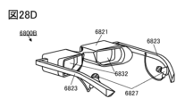
- 28A to 28D are diagrams illustrating an example of an electronic device according to an embodiment.
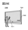
- 29A to 29F are diagrams illustrating an example of an electronic device according to an embodiment.
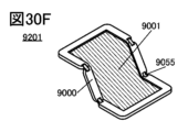
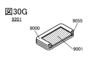
- 30A to 30G are diagrams illustrating an example of an electronic device according to an embodiment.
- the light-emitting device of one aspect of the present invention is a light-emitting device having a first light source and a first conversion unit.
- the first light source overlaps with the first conversion unit, and the first light source irradiates the first conversion unit with a first light, and the first light has a spectrum having an intensity at a first wavelength.
- the first conversion unit has a first layer and a second layer, and the first layer is sandwiched between the second layer and the first light source.
- the first layer converts the first light to a second light, and the second light has a spectrum having a peak at the second wavelength.
- the second wavelength is longer than the first wavelength, and the second layer has a reflectance of 0.8 to 1.0 at the first wavelength, and the second layer has a transmittance of 0.8 to 1.0 at the second wavelength.
- the first layer can convert the first light emitted by the first light source into the second light.
- the second layer can reflect the first light that has passed through the first layer and reached the second layer toward the first layer.
- the first layer can convert the first light reflected by the second layer into the second light.
- the first light emitted by the first light source can be efficiently converted into the second light.
- blue light can be efficiently converted into green light or red light.
- Figure 1 is a cross-sectional view illustrating the configuration of a light-emitting device according to one embodiment of the present invention.
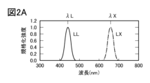
- Figure 2A is a diagram illustrating an emission spectrum according to a configuration of a light-emitting device of one embodiment of the present invention.
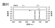
- Figures 2B and 2C are diagrams illustrating wavelength-transmittance characteristics and wavelength-reflectance characteristics according to a configuration of a light-emitting device of one embodiment of the present invention
- Figure 2D is a diagram illustrating wavelength-transmittance characteristics according to a configuration of a light-emitting device of one embodiment of the present invention.
- One embodiment of the present invention is a light-emitting device having a light source LSX and a conversion unit CUX (see FIG. 1).
- the light source LSX overlaps with the conversion unit CUX, and the light source LSX irradiates the conversion unit CUX with light LL.
- the light LL has a spectrum having an intensity at a wavelength ⁇ L (see FIG. 2A). In other words, the light LL includes light of a wavelength ⁇ L.
- a light emitting diode can be used as the light source LSX. This makes it possible to achieve high reliability, high brightness, and high current efficiency.
- an organic light emitting diode can be used as the light source LSX.
- OLED organic light emitting diode
- the light LL includes blue light.
- the light LL includes light having a wavelength of 380 nm or more and 480 nm or less, and preferably has a spectrum with a maximum peak in the range of 380 nm or more and 480 nm or less.
- the light LL can also include blue light and green light. Or, the light LL can also include blue light, green light, and red light. This makes it easier to select materials related to the light emission of the light source LSX. Also, the light emission efficiency of the light source LSX can be increased.
- the conversion unit CUX comprises a layer CCX and a layer DMX1 (see FIG. 1).
- the layer CCX is sandwiched between the layer DMX1 and the light source LSX.
- the layer CCX has a function of converting the light LL into light LX.
- the light LX has a spectrum having a peak at a wavelength ⁇ X, which is longer than the wavelength ⁇ L (see FIG. 2A).
- the layer CCX converts the light of wavelength ⁇ L contained in the light LL into light having a wavelength ⁇ X longer than the wavelength ⁇ L.
- the spectrum of the light LX has a peak at the wavelength ⁇ X.
- a phosphor can be used in the layer CCX.
- the layer DMX1 has a reflectance of 0.8 or more and 1.0 or less at the wavelength ⁇ L (see FIG. 2B).
- the layer DMX1 also has a transmittance of 0.8 or more and 1.0 or less at the wavelength ⁇ X.
- the reflectance of the layer DMX1 at the wavelength ⁇ L is preferably as close to 1.0 as possible, and if it is lower than 0.8, the loss of the light LL becomes significant.
- the transmittance of the layer DMX1 at the wavelength ⁇ X is preferably as close to 1.0 as possible, and if it is lower than 0.8, the loss of the light LX becomes significant.
- the layer CCX can convert the light LL emitted by the light source LSX into light LX.
- the layer DMX1 can reflect the light LL that has passed through the layer CCX and reached the layer DMX1 toward the layer CCX.
- the layer CCX can convert the light LL reflected by the layer DMX1 into light LX.
- the light LL emitted by the light source LSX can be efficiently converted into light LX.
- blue light can be efficiently converted into green light or red light.
- the layer CCX can convert the light LL emitted by the light source LSX into light LX having a narrow spectrum with a full width at half maximum.
- the layer CCX can convert the light LL emitted by the light source LSX into light LX having high saturation.
- a novel light-emitting device with excellent convenience, usefulness, and reliability can be provided.
- the layer DMX1 includes layers DMX11, DMX12, and DMX13 (see FIG. 3A).
- the layer DMX12 is sandwiched between the layers DMX11 and DMX13.
- the layer DMX1 includes three or more layers, and preferably includes five or more layers. This allows the reflectance at a predetermined wavelength to be 0.8 or more. Also, the transmittance at another predetermined wavelength to be 0.8 or more. The more layers there are, the higher the reflectance can be obtained, and the narrower the full width at half maximum of the bandpass filter can be.
- the refractive index at the wavelength ⁇ L in the film state corresponds to the value measured by preparing a sample in which a target layer (for example, a layer corresponding to the layer DMX12) is formed on a Si wafer and measuring the sample using a spectroscopic ellipsometer.
- a target layer for example, a layer corresponding to the layer DMX12
- silicon oxide abbreviated as SiO2
- magnesium fluoride abbreviated as MgF2
- lithium fluoride LiF
- sodium fluoride NaF
- titanium oxide, silicon nitride (SiNx: x is any number greater than 0), aluminum oxide, zirconium oxide, or hafnium oxide can be used as a material having a refractive index of 1.6 or more in the film state.
- layers DMX11 and DMX13 both have a refractive index of less than 1.6 at wavelength ⁇ L in the film state.
- the layer DMX1 can form a dielectric multilayer film. Furthermore, the layer DMX1 can have a predetermined reflectance at the wavelength ⁇ L and a predetermined transmittance at the wavelength ⁇ X. As a result, a novel light-emitting device that is highly convenient, useful, and reliable can be provided.
- the conversion unit CUX comprises a layer DMX2 (see FIG. 1), which is sandwiched between a layer CCX and a light source LSX.
- the layer DMX2 has a transmittance of 0.8 or more and 1.0 or less at the wavelength ⁇ L (see FIG. 2C).
- the layer DMX2 has a reflectance of 0.8 or more and 1.0 or less at the wavelength ⁇ X.
- the layer DMX2 can reflect the light LX that has passed through the layer CCX and reached the layer DMX2 toward the layer CCX. Furthermore, the light LX can be efficiently extracted from the light emitting device. Furthermore, the light LL emitted by the light source LSX can be efficiently converted into light LX. As a result, a novel light emitting device that is highly convenient, useful, and reliable can be provided.
- the layer DMX2 includes a layer DMX21, a layer DMX22, and a layer DMX23 (see FIG. 3B).
- the layer DMX22 is sandwiched between the layer DMX21 and the layer DMX23.
- the layer DMX2 includes three or more layers, and preferably includes five or more layers. This allows the reflectance at a predetermined wavelength to be 0.8 or more. Also, the transmittance at another predetermined wavelength to be 0.8 or more. The more layers there are, the higher the reflectance can be obtained, and the narrower the full width at half maximum of the bandpass filter can be.
- layers DMX21 and DMX23 both have a refractive index of 1.6 or more at wavelength ⁇ X in the film state.
- layers DMX21 and DMX23 both have a refractive index of less than 1.6 at wavelength ⁇ X in the film state.
- the layer DMX2 can be configured as a dielectric multilayer film. Furthermore, the layer DMX2 can have a predetermined transmittance at the wavelength ⁇ L and a predetermined reflectance at the wavelength ⁇ X. As a result, a novel light-emitting device that is highly convenient, useful, and reliable can be provided.
- the conversion unit CUX comprises a layer CFX (see FIG. 1).
- the layer DMX1 is sandwiched between the layer CFX and the light source LSX.
- the layer CFX has a transmittance greater than 0 and equal to or less than 0.2 at the wavelength ⁇ L (see FIG. 2D).
- the layer CFX also has a transmittance greater than 0.6 and equal to or less than 1.0 at the wavelength ⁇ X.
- the transmittance of the layer CFX at the wavelength ⁇ L is preferably closer to 0, and if it is higher than 0.2, the light LL leaks out of the light emitting device.
- the transmittance of the layer CFX at the wavelength ⁇ X is preferably closer to 1.0, and if it is lower than 0.6, the efficiency of extracting the light LX from the light emitting device decreases.
- the full width at half maximum of the reflection spectrum of the layer DMX2 is narrower than the full width at half maximum of the transmission spectrum of the layer CFX.
- Figure 4 is a cross-sectional view illustrating the configuration of a light source LSX that can be used in a light-emitting device according to one embodiment of the present invention.
- the configuration of the light source LSX described in this embodiment can be used in the display device of one embodiment of the present invention.
- the symbol “X” used in the configuration of the light source LSX can be read as “A” and can be used in the description of the light source LSA.
- the symbol “X” can be read as "B” or "C” and the configuration of the light source LSX can be applied to the light source LSB or light source LSC.
- the light source LSX described in this embodiment has an electrode 551X, an electrode 552X, and a unit 103X.
- the electrode 552X overlaps with the electrode 551X, and the unit 103X is sandwiched between the electrode 552X and the electrode 551X.
- the unit 103X has a single-layer structure or a laminated structure.
- the unit 103X includes a layer 111X, a layer 112X, and a layer 113X (see FIG. 4).
- the unit 103X has a function of emitting light LL.
- Layer 111X is sandwiched between layers 113X and 112X, layer 113X is sandwiched between electrode 552X and layer 111X, and layer 112X is sandwiched between layer 111X and electrode 551X.
- a layer selected from functional layers such as a light-emitting layer, a hole transport layer, an electron transport layer, and a carrier block layer can be used in unit 103X.
- a layer selected from functional layers such as a hole injection layer, an electron injection layer, an exciton block layer, and a charge generation layer can be used in unit 103X.
- a material having a hole transporting property can be used for the layer 112X.
- the layer 112X can be referred to as a hole transporting layer.
- a material having a larger band gap than that of the light-emitting material contained in the layer 111X is preferably used for the layer 112X. This can suppress energy transfer from excitons generated in the layer 111X to the layer 112X.
- a material having a hole mobility of 1 ⁇ 10 ⁇ 6 cm 2 /Vs or more can be suitably used as the material having a hole transport property.
- an amine compound or an organic compound having a ⁇ -electron-rich heteroaromatic ring skeleton can be used as a material having hole transport properties.
- a compound having an aromatic amine skeleton, a compound having a carbazole skeleton, a compound having a thiophene skeleton, a compound having a furan skeleton, etc. can be used.
- a compound having an aromatic amine skeleton or a compound having a carbazole skeleton is preferable because it has good reliability, has high hole transport properties, and contributes to reducing the driving voltage.
- Examples of compounds having an aromatic amine skeleton include 4,4'-bis[N-(1-naphthyl)-N-phenylamino]biphenyl (abbreviation: NPB), N,N'-diphenyl-N,N'-bis(3-methylphenyl)-4,4'-diaminobiphenyl (abbreviation: TPD), N,N'-bis(9,9'-spirobi[9H-fluorene]-2-yl)-N,N'-diphenyl-4,4'-diaminobiphenyl (abbreviation: BSPB), 4-phenyl-4'-(9-phenylfluorene-9-yl)triphenylamine (abbreviation: BPAFLP), 4-phenyl-3'-(9-phenylfluorene-9-yl)triphenylamine (abbreviation: mBPAFLP), 4-phenyl-4'-(9-phenyl-9H
- Examples of compounds having a carbazole skeleton that can be used include 1,3-bis(N-carbazolyl)benzene (abbreviation: mCP), 4,4'-di(N-carbazolyl)biphenyl (abbreviation: CBP), 3,6-bis(3,5-diphenylphenyl)-9-phenylcarbazole (abbreviation: CzTP), and 3,3'-bis(9-phenyl-9H-carbazole) (abbreviation: PCCP).
- mCP 1,3-bis(N-carbazolyl)benzene
- CBP 4,4'-di(N-carbazolyl)biphenyl
- CzTP 3,6-bis(3,5-diphenylphenyl)-9-phenylcarbazole
- PCCP 3,3'-bis(9-phenyl-9H-carbazole
- Examples of compounds having a thiophene skeleton that can be used include 4,4',4''-(benzene-1,3,5-triyl)tri(dibenzothiophene) (abbreviation: DBT3P-II), 2,8-diphenyl-4-[4-(9-phenyl-9H-fluoren-9-yl)phenyl]dibenzothiophene (abbreviation: DBTFLP-III), 4-[4-(9-phenyl-9H-fluoren-9-yl)phenyl]-6-phenyldibenzothiophene (abbreviation: DBTFLP-IV), etc.
- DBT3P-II 4,4',4''-(benzene-1,3,5-triyl)tri(dibenzothiophene)
- DBTFLP-III 2,8-diphenyl-4-[4-(9-phenyl-9H-fluoren-9-yl)phenyl]
- Examples of compounds having a furan skeleton that can be used include 4,4',4''-(benzene-1,3,5-triyl)tri(dibenzofuran) (abbreviation: DBF3P-II), 4- ⁇ 3-[3-(9-phenyl-9H-fluoren-9-yl)phenyl]phenyl ⁇ dibenzofuran (abbreviation: mmDBFFLBi-II), etc.
- a material having an electron transporting property a material having an anthracene skeleton, a mixed material, or the like can be used for the layer 113X.
- the layer 113X can be referred to as an electron transporting layer.
- a material having a larger band gap than that of the light-emitting material contained in the layer 111X is preferably used for the layer 113X. This can suppress energy transfer from excitons generated in the layer 111X to the layer 113X.
- Electrode-transporting material For example, a material having an electron mobility of 1 ⁇ 10 ⁇ 7 cm 2 /Vs or more and 5 ⁇ 10 ⁇ 5 cm 2 /Vs or less under the condition that the square root of the electric field strength V/cm is 600 can be suitably used as a material having electron transport properties. This makes it possible to suppress the transport properties of electrons in the electron transport layer. Alternatively, it is possible to control the amount of electrons injected into the light-emitting layer. Alternatively, it is possible to prevent the light-emitting layer from becoming in an electron-excess state.
- a metal complex or an organic compound having a ⁇ -electron-deficient heteroaromatic ring skeleton can be used as a material with electron transport properties.
- metal complexes examples include bis(10-hydroxybenzo[h]quinolinato)beryllium(II) (abbreviation: BeBq2 ), bis(2-methyl-8-quinolinolato)(4-phenylphenolato)aluminum(III) (abbreviation: BAlq), bis(8-quinolinolato)zinc(II) (abbreviation: Znq), bis[2-(2-benzoxazolyl)phenolato]zinc(II) (abbreviation: ZnPBO), bis[2-(2-benzothiazolyl)phenolato]zinc(II) (abbreviation: ZnBTZ), and the like.
- heterocyclic compounds having a polyazole skeleton for example, heterocyclic compounds having a diazine skeleton, heterocyclic compounds having a pyridine skeleton, heterocyclic compounds having a triazine skeleton, etc. can be used.
- heterocyclic compounds having a diazine skeleton or heterocyclic compounds having a pyridine skeleton are preferable because of their good reliability.
- heterocyclic compounds having a diazine (pyrimidine or pyrazine) skeleton have high electron transport properties and can reduce the driving voltage.
- heterocyclic compounds having a polyazole skeleton examples include 2-(4-biphenylyl)-5-(4-tert-butylphenyl)-1,3,4-oxadiazole (abbreviation: PBD), 3-(4-biphenylyl)-4-phenyl-5-(4-tert-butylphenyl)-1,2,4-triazole (abbreviation: TAZ), 1,3-bis[5-(p-tert-butylphenyl)-1,3,4-oxadiazol-2-yl]benzene (abbreviation: O XD-7), 9-[4-(5-phenyl-1,3,4-oxadiazol-2-yl)phenyl]-9H-carbazole (abbreviation: CO11), 2,2',2''-(1,3,5-benzenetriyl)tris(1-phenyl-1H-benzimidazole) (abbreviation: TPBI), 2-[3-(
- heterocyclic compounds having a diazine skeleton examples include 2-[3-(dibenzothiophen-4-yl)phenyl]dibenzo[f,h]quinoxaline (abbreviation: 2mDBTPDBq-II), 2-[3-(3'-dibenzothiophen-4-yl)biphenyl]dibenzo[f,h]quinoxaline (abbreviation: 2mDBTBPDBq-II), 2-[3'-(9H-carbazol-9-yl)biphenyl-3-yl]dibenzo[f,h]quinoxaline (abbreviation: 2mDBTBPDBq-II), Noxaline (abbreviation: 2mCzBPDBq), 4,6-bis[3-(phenanthren-9-yl)phenyl]pyrimidine (abbreviation: 4,6mPnP2Pm), 4,6-bis[3-(4-dibenzothienyl
- heterocyclic compounds having a pyridine skeleton include 3,5-bis[3-(9H-carbazol-9-yl)phenyl]pyridine (abbreviation: 35DCzPPy), 1,3,5-tri[3-(3-pyridyl)phenyl]benzene (abbreviation: TmPyPB), and the like.
- heterocyclic compounds having a triazine skeleton examples include 2-[3'-(9,9-dimethyl-9H-fluoren-2-yl)biphenyl-3-yl]-4,6-diphenyl-1,3,5-triazine (abbreviation: mFBPTzn), 2-(biphenyl-4-yl)-4-phenyl-6-(9,9'-spirobi[9H-fluoren]-2-yl)-1,3,5-triazine (abbreviation: BP-SFTzn).
- mFBPTzn 2-(biphenyl-4-yl)-4-phenyl-6-(9,9'-spirobi[9H-fluoren]-2-yl)-1,3,5-triazine
- An organic compound having an anthracene skeleton can be used for the layer 113X.
- an organic compound containing both an anthracene skeleton and a heterocyclic skeleton can be suitably used.
- an organic compound containing both an anthracene skeleton and a nitrogen-containing five-membered ring skeleton can be used for layer 113X.
- an organic compound containing both an anthracene skeleton and a nitrogen-containing five-membered ring skeleton containing two heteroatoms in the ring can be used for layer 113X.
- a pyrazole ring, an imidazole ring, an oxazole ring, a thiazole ring, or the like can be suitably used for the heterocyclic skeleton.
- an organic compound containing both an anthracene skeleton and a nitrogen-containing six-membered ring skeleton can be used for layer 113X.
- an organic compound containing both an anthracene skeleton and a nitrogen-containing six-membered ring skeleton containing two heteroatoms in the ring can be used for layer 113X.
- a pyrazine ring, a pyrimidine ring, a pyridazine ring, or the like can be suitably used for the heterocyclic skeleton.
- a mixture of a plurality of substances can be used for the layer 113X.
- a mixture of an alkali metal, an alkali metal compound, or an alkali metal complex, and a substance having an electron-transporting property can be used for the layer 113X.
- the HOMO (Highest Occupied Molecular Orbital) level of the material having an electron-transporting property is more preferably ⁇ 6.0 eV or higher.
- the composite material described in embodiment 3 can be preferably used for the layer 113X in combination with a structure in which the composite material is used for the layer 104X.
- a composite material of a substance having an electron-accepting property and a material having a hole-transporting property can be used for the layer 104X.
- a composite material of a substance having an electron-accepting property and a substance having a relatively deep HOMO level HM1 of -5.7 eV or more and -5.4 eV or less can be used for the layer 104X.
- a structure in which the mixed material is used in layer 113X and the above composite material is used in layer 104X with a structure in which a material having hole transport properties is used in layer 112X.
- a substance having a HOMO level HM2 in the range of -0.2 eV to 0 eV with respect to the above relatively deep HOMO level HM1 can be used in layer 112X. This can improve the reliability of the light-emitting device.
- the above light-emitting device may be referred to as a Recombination-Site Tailoring Injection structure (ReSTI structure).
- the alkali metal, alkali metal compound, or alkali metal complex exists with a concentration difference (including 0) in the thickness direction of layer 113X.
- a metal complex containing an 8-hydroxyquinolinato structure can be used.
- a methyl-substituted metal complex containing an 8-hydroxyquinolinato structure e.g., a 2-methyl-substituted or 5-methyl-substituted metal complex
- a metal complex containing an 8-hydroxyquinolinato structure e.g., a 2-methyl-substituted or 5-methyl-substituted metal complex
- 8-hydroxyquinolinato-lithium abbreviation: Liq
- 8-hydroxyquinolinato-sodium abbreviation: Naq
- complexes of monovalent metal ions, especially lithium complexes are preferred, with Liq being more preferred.
- a light-emitting material or a light-emitting material and a host material can be used for the layer 111X.
- the layer 111X can be called a light-emitting layer. Note that a configuration in which the layer 111X is disposed in a region where holes and electrons recombine is preferable. This allows the energy generated by the recombination of carriers to be efficiently converted into light and emitted.
- layer 111X away from metals used in electrodes, etc. This makes it possible to suppress the quenching phenomenon caused by metals used in electrodes, etc.
- a microresonator structure can be formed by placing layer 111X at an appropriate position between the electrodes, etc.
- a fluorescent material for example, a fluorescent material, a phosphorescent material, or a material that exhibits thermally activated delayed fluorescence (TADF) (also called a TADF material) can be used as the luminescent material.
- TADF thermally activated delayed fluorescence
- fluorescent material A fluorescent substance can be used for the layer 111X.
- the following fluorescent substances can be used for the layer 111X.
- the present invention is not limited thereto, and various known fluorescent substances can be used for the layer 111X.
- condensed aromatic diamine compounds such as pyrene diamine compounds, such as 1,6FLPAPrn, 1,6mMemFLPAPrn, and 1,6BnfAPrn-03, are preferred because they have high hole trapping properties and excellent luminous efficiency or reliability.
- N-[4-(9,10-diphenyl-2-anthryl)phenyl]-N,N',N'-triphenyl-1,4-phenylenediamine abbreviation: 2DPAPPA
- N,N,N',N',N'',N'',N'',N''',N'''-octaphenyldibenzo[g,p]chrysene-2,7,10,15-tetraamine abmarin 30, 9,10-diphenyl-2-[N-phenyl-N-(9-phenyl-carbazol-3-yl)-amino]-anthracene (abbreviation: 2PCAPA), N-[9,10-bis(biphenyl-2-yl)-2-anthryl]-N,9-diphenyl-9H-carbazol-3-amine (abbreviation: 2PCABPhA), N-(9,10-diphenyl-9H-carbazol-3
- DCM1 2-(2- ⁇ 2-[4-(dimethylamino)phenyl]ethenyl ⁇ -6-methyl-4H-pyran-4-ylidene)propanedinitrile
- DCM2 2- ⁇ 2-methyl-6-[2-(2,3,6,7-tetrahydro-1H,5H-benzo[ij]quinolizin-9-yl)ethenyl]-4H-pyran-4-ylidene ⁇ propanedinitrile
- DCM2 N,N,N',N'-tetrakis(2-methyl-6-[2-(2,3,6,7-tetrahydro-1H,5H-benzo[ij]quinolizin-9-yl)ethenyl]-4H-pyran-4-ylidene ⁇ propanedinitrile
- DCM2 p-mPhTD
- a phosphorescent material can be used for the layer 111X.
- the phosphorescent material exemplified below can be used for the layer 111X. Note that the present invention is not limited thereto, and various known phosphorescent materials can be used for the layer 111X.
- organometallic iridium complexes having a 4H-triazole skeleton organometallic iridium complexes having a 1H-triazole skeleton, organometallic iridium complexes having an imidazole skeleton, organometallic iridium complexes having a phenylpyridine derivative having an electron-withdrawing group as a ligand, organometallic iridium complexes having a pyrimidine skeleton, organometallic iridium complexes having a pyrazine skeleton, organometallic iridium complexes having a pyridine skeleton, rare earth metal complexes, platinum complexes, and the like can be used for layer 111X.
- organometallic iridium complex having a 4H-triazole skeleton examples include tris ⁇ 2-[5-(2-methylphenyl)-4-(2,6-dimethylphenyl)-4H-1,2,4-triazol-3-yl- ⁇ N2]phenyl- ⁇ C ⁇ iridium(III) (abbreviation: [Ir(mpptz-dmp) 3 ]), tris(5-methyl-3,4-diphenyl-4H-1,2,4-triazolato)iridium(III) (abbreviation: [Ir(Mptz) 3 ]), tris[4-(3-biphenyl)-5-isopropyl-3-phenyl-4H-1,2,4-triazolato]iridium(III) (abbreviation: [Ir(iPrptz-3b) 3 ]), and the like.
- organometallic iridium complexes having a 1H-triazole skeleton examples include tris[3-methyl-1-(2-methylphenyl)-5-phenyl-1H-1,2,4-triazolato]iridium(III) (abbreviation: [Ir(Mptz1-mp) 3 ]), tris(1-methyl-5-phenyl-3-propyl-1H-1,2,4-triazolato)iridium(III) (abbreviation: [Ir(Prptz1-Me) 3 ]), and the like.
- organometallic iridium complexes having an imidazole skeleton examples include fac-tris[1-(2,6-diisopropylphenyl)-2-phenyl-1H-imidazole]iridium(III) (abbreviation: [Ir(iPrpim) 3 ]), tris[3-(2,6-dimethylphenyl)-7-methylimidazo[1,2-f]phenanthridinato]iridium(III) (abbreviation: [Ir(dmpimpt-Me) 3 ]), and the like.
- organometallic iridium complexes having a phenylpyridine derivative having an electron-withdrawing group as a ligand include bis[2-(4',6'-difluorophenyl)pyridinato-N,C2 ' ]iridium(III) tetrakis(1-pyrazolyl)borate (abbreviation: FIr6), bis[2-(4',6'-difluorophenyl)pyridinato-N,C2 ' ]iridium(III) picolinate (abbreviation: FIrpic), bis ⁇ 2-[3',5'-bis(trifluoromethyl)phenyl]pyridinato-N, C2' ⁇ iridium(III) picolinate (abbreviation: [Ir( CF3ppy ) 2 (pic)]), and bis[2-(4',6'-difluorophenyl)pyridinato-N,C2 '
- These compounds emit blue phosphorescence and have a peak emission wavelength between 440 nm and 520 nm.
- organometallic iridium complexes having a pyrimidine skeleton examples include tris(4-methyl-6-phenylpyrimidinato)iridium(III) (abbreviation: [Ir(mppm) 3 ]), tris(4-t-butyl-6-phenylpyrimidinato)iridium(III) (abbreviation: [Ir(tBuppm) 3 ]), (acetylacetonato)bis(6-methyl-4-phenylpyrimidinato)iridium(III) (abbreviation: [Ir(mppm) 2 (acac)]), (acetylacetonato)bis(6-tert-butyl-4-phenylpyrimidinato)iridium(III) (abbreviation: [Ir(tBuppm) 2 (acac)]), (acetylacetonato)bis[6-(2-norbornyl)
- organometallic iridium complexes having a pyrazine skeleton examples include (acetylacetonato)bis(3,5-dimethyl-2-phenylpyrazinato)iridium(III) (abbreviation: [Ir(mppr-Me) 2 (acac)]), (acetylacetonato)bis(5-isopropyl-3-methyl-2-phenylpyrazinato)iridium(III) (abbreviation: [Ir(mppr-iPr) 2 (acac)]), and the like.
- organometallic iridium complexes having a pyridine skeleton examples include tris(2-phenylpyridinato-N,C 2′ )iridium(III) (abbreviation: [Ir(ppy) 3 ]), bis(2-phenylpyridinato-N,C 2′ )iridium(III) acetylacetonate (abbreviation: [Ir(ppy) 2 (acac) ]), bis(benzo[h]quinolinato)iridium(III) acetylacetonate (abbreviation: [Ir(bzq) 2 (acac) ]), tris(benzo[h]quinolinato)iridium(III) (abbreviation: [Ir(bzq) 3 ]), and tris(2-phenylquinolinato-N,C 2′ )iridium(III) (abbreviation: [Ir(pq) 3 ]), bis(2-phenylquinolinato-
- rare earth metal complexes examples include tris(acetylacetonato)(monophenanthroline)terbium(III) (abbreviation: [Tb(acac) 3 (Phen)]).
- organometallic iridium complexes with a pyrimidine skeleton are remarkably superior in terms of reliability and luminous efficiency.
- organometallic iridium complexes having a pyrimidine skeleton examples include (diisobutyrylmethanato)bis[4,6-bis(3-methylphenyl)pyrimidinato]iridium(III) (abbreviation: [Ir(5mdppm) 2 (dibm)]), bis[4,6-bis(3-methylphenyl)pyrimidinato](dipivaloylmethanato)iridium(III) (abbreviation: [Ir(5mdppm) 2 (dpm)]), and bis[4,6-di(naphthalen-1-yl)pyrimidinato](dipivaloylmethanato)iridium(III) (abbreviation: [Ir(d1npm) 2 (dpm)]).
- organometallic iridium complexes having a pyrazine skeleton examples include (acetylacetonato)bis(2,3,5-triphenylpyrazinato)iridium(III) (abbreviation: [Ir(tppr) 2 (acac)]), bis(2,3,5-triphenylpyrazinato)(dipivaloylmethanato)iridium(III) (abbreviation: [Ir(tppr) 2 (dpm)]), (acetylacetonato)bis[2,3-bis(4-fluorophenyl)quinoxalinato]iridium(III) (abbreviation: [Ir(Fdpq) 2 (acac)]), and the like.
- organometallic iridium complexes having a pyridine skeleton examples include tris(1-phenylisoquinolinato-N,C2 ' )iridium(III) (abbreviation: [Ir(piq) 3 ]), bis(1-phenylisoquinolinato-N,C2 ' )iridium(III) acetylacetonate (abbreviation: [Ir(piq) 2 (acac)]), and the like.
- rare earth metal complexes examples include tris(1,3-diphenyl-1,3-propanedionato)(monophenanthroline)europium(III) (abbreviation: [Eu(DBM) 3 (Phen)]), tris[1-(2-thenoyl)-3,3,3-trifluoroacetonato](monophenanthroline)europium(III) (abbreviation: [Eu(TTA) 3 (Phen)]), and the like.
- platinum complexes examples include 2,3,7,8,12,13,17,18-octaethyl-21H,23H-porphyrin platinum(II) (abbreviation: PtOEP).
- organometallic iridium complexes having a pyrazine skeleton can emit red light with a chromaticity suitable for use in display devices.
- a TADF material can be used for the layer 111X.
- the S1 level of the host material is preferably higher than the S1 level of the TADF material.
- the T1 level of the host material is preferably higher than the T1 level of the TADF material.
- the TADF materials shown below can be used as the luminescent material. However, this is not limited to these, and various known TADF materials can be used.
- the difference between the S1 level and the T1 level of the TADF material is small, and a small amount of thermal energy can cause reverse intersystem crossing (upconversion) from the triplet excited state to the singlet excited state. This allows the singlet excited state to be generated efficiently from the triplet excited state. In addition, the triplet excited energy can be converted into light emission.
- exciplexes also called exciplexes
- TADF materials that can convert triplet excitation energy into singlet excitation energy
- the phosphorescence spectrum observed at low temperatures may be used as an index of the T1 level.
- the TADF material when a tangent line is drawn at the short-wavelength tail of the fluorescence spectrum, and the energy of the wavelength of the extrapolated line is taken as the S1 level, and a tangent line is drawn at the short-wavelength tail of the phosphorescence spectrum, and the energy of the wavelength of the extrapolated line is taken as the T1 level, the difference between the S1 level and the T1 level is preferably 0.3 eV or less, and more preferably 0.2 eV or less.
- fullerene and its derivatives, acridine and its derivatives, eosin derivatives, etc. can be used as TADF materials.
- metal-containing porphyrins containing magnesium (Mg), zinc (Zn), cadmium (Cd), tin (Sn), platinum (Pt), indium (In), palladium (Pd), etc. can be used as TADF materials.
- protoporphyrin-tin fluoride complex SnF2 (Proto IX)
- mesoporphyrin-tin fluoride complex SnF2 (Meso IX)
- hematoporphyrin-tin fluoride complex SnF2 (Hemato IX)
- coproporphyrin tetramethyl ester-tin fluoride complex SnF2 (Copro III-4Me)
- octaethylporphyrin-tin fluoride complex SnF2 (OEP)
- etioporphyrin-tin fluoride complex SnF2 (Etio I)
- octaethylporphyrin-platinum chloride complex PtCl2 OEP
- a heterocyclic compound having one or both of a ⁇ -electron rich heteroaromatic ring and a ⁇ -electron deficient heteroaromatic ring can be used as a TADF material.
- the structural formulas are as follows: 2-(biphenyl-4-yl)-4,6-bis(12-phenylindolo[2,3-a]carbazol-11-yl)-1,3,5-triazine (abbreviation: PIC-TRZ), 9-(4,6-diphenyl-1,3,5-triazin-2-yl)-9'-phenyl-9H,9'H-3,3'-bicarbazole (abbreviation: PCCzTzn), 2- ⁇ 4-[3-(N-phenyl-9H-carbazol-3-yl)-9H-carbazol-9-yl]phenyl ⁇ -4,6-diphenyl-1,3,5-triazine (abbreviation: PCCzPTzn), 2-[4-(10H-phenoxazin-10-yl)phenyl]-4 ,6-diphenyl-1,3,5-triazine (abbreviation: PXZ-TRZ), 3-[4--(
- the heterocyclic compound has a ⁇ -electron rich heteroaromatic ring and a ⁇ -electron deficient heteroaromatic ring, and therefore has high electron transport and hole transport properties, and is therefore preferred.
- the pyridine skeleton, the diazine skeleton (pyrimidine skeleton, pyrazine skeleton, pyridazine skeleton), and the triazine skeleton are preferred because they are stable and have good reliability.
- the benzofuropyrimidine skeleton, the benzothienopyrimidine skeleton, the benzofuropyrazine skeleton, and the benzothienopyrazine skeleton are preferred because they have high electron accepting properties and good reliability.
- the skeletons having a ⁇ -electron-rich heteroaromatic ring it is preferable to have at least one of the acridine skeleton, phenoxazine skeleton, phenothiazine skeleton, furan skeleton, thiophene skeleton, and pyrrole skeleton, since they are stable and reliable.
- the furan skeleton the dibenzofuran skeleton is preferable
- the thiophene skeleton the dibenzothiophene skeleton is preferable.
- the indole skeleton, the carbazole skeleton, the indolocarbazole skeleton, the bicarbazole skeleton, and the 3-(9-phenyl-9H-carbazol-3-yl)-9H-carbazole skeleton are particularly preferable.
- a substance in which a ⁇ -electron-rich heteroaromatic ring and a ⁇ -electron-deficient heteroaromatic ring are directly bonded is particularly preferred because the electron donating property of the ⁇ -electron-rich heteroaromatic ring and the electron accepting property of the ⁇ -electron-deficient heteroaromatic ring are both strong, and the energy difference between the S1 level and the T1 level is small, so that thermally activated delayed fluorescence can be efficiently obtained.
- an aromatic ring bonded to an electron-withdrawing group such as a cyano group may be used instead of the ⁇ -electron-deficient heteroaromatic ring.
- an aromatic amine skeleton, a phenazine skeleton, or the like can be used as the ⁇ -electron-rich skeleton.
- examples of ⁇ -electron-deficient skeletons that can be used include a xanthene skeleton, a thioxanthene dioxide skeleton, an oxadiazole skeleton, a triazole skeleton, an imidazole skeleton, an anthraquinone skeleton, a boron-containing skeleton such as phenylborane or boranthrene, an aromatic ring or a heteroaromatic ring having a nitrile group or a cyano group such as benzonitrile or cyanobenzene, a carbonyl skeleton such as benzophenone, a phosphine oxide skeleton, and a sulfone skeleton.
- a ⁇ -electron deficient skeleton and a ⁇ -electron rich skeleton can be used in place of at least one of a ⁇ -electron deficient heteroaromatic ring and a ⁇ -electron rich heteroaromatic ring.
- a material having carrier transport properties can be used as the host material.
- a material having hole transport properties, a material having electron transport properties, a material exhibiting thermally activated delayed fluorescence (TADF), a material having an anthracene skeleton, a mixed material, or the like can be used as the host material.
- TADF thermally activated delayed fluorescence
- a material having an anthracene skeleton, a mixed material, or the like can be used as the host material.
- TADF thermally activated delayed fluorescence
- a material having an anthracene skeleton a mixed material, or the like
- a material having a band gap larger than that of the light-emitting material contained in the layer 111X is preferably used as the host material. This can suppress energy transfer from excitons generated in the layer 111X to the host material.
- a material having a hole-transporting property with a hole mobility of 1 ⁇ 10 ⁇ 6 cm 2 /Vs or more can be preferably used as the material having a hole-transporting property.
- a material having a hole-transporting property that can be used for the layer 112X can be used for the layer 111X.
- a metal complex or an organic compound having a ⁇ -electron-deficient heteroaromatic ring skeleton can be used as the material having an electron-transporting property.
- a material having an electron-transporting property that can be used for the layer 113X can be used for the layer 111X.
- An organic compound having an anthracene skeleton can be used as a host material.
- an organic compound having an anthracene skeleton is suitable. This makes it possible to realize a light-emitting device having good light-emitting efficiency and durability.
- a diphenylanthracene skeleton particularly an organic compound having a 9,10-diphenylanthracene skeleton
- it is preferred because it is chemically stable.
- the host material has a carbazole skeleton
- it is preferred because it enhances the hole injection and transport properties.
- the HOMO level is shallower by about 0.1 eV than a host material having a carbazole skeleton, making it easier for holes to enter, and it is also preferable because it has excellent hole transport properties and high heat resistance.
- a benzofluorene skeleton or a dibenzofluorene skeleton may be used instead of the carbazole skeleton.
- a substance having both a 9,10-diphenylanthracene skeleton and a carbazole skeleton, a substance having both a 9,10-diphenylanthracene skeleton and a benzocarbazole skeleton, and a substance having both a 9,10-diphenylanthracene skeleton and a dibenzocarbazole skeleton are preferable as host materials.
- 6-[3-(9,10-diphenyl-2-anthryl)phenyl]-benzo[b]naphtho[1,2-d]furan abbreviation: 2mBnfPPA
- 9-phenyl-10-[4'-(9-phenyl-9H-fluoren-9-yl)biphenyl-4-yl]anthracene abbreviation: FLPPA
- 9-(1-naphthyl)-10-[4-(2-naphthyl)phenyl]anthracene abbreviation: ⁇ N- ⁇ NPAnth
- PCzPA 9-[4-(9-phenylcarbazole -3-yl)]phenyl-10-phenylanthracene
- CzPA 7-[4-[4-(10-phenyl-9-anthracenyl)phenyl]-9H-carbazole
- CzPA, cgDBCzPA, 2mBnfPPA, and PCzPA show very good properties.
- the TADF material can be used as a host material.
- the triplet excitation energy generated in the TADF material can be converted into singlet excitation energy by reverse intersystem crossing. Furthermore, the excitation energy can be transferred to a light-emitting material.
- the TADF material functions as an energy donor, and the light-emitting material functions as an energy acceptor. This can increase the luminous efficiency of a light-emitting device.
- the luminescent material is a fluorescent luminescent material.
- the S1 level of the TADF material is higher than the S1 level of the fluorescent luminescent material.
- the T1 level of the TADF material is higher than the S1 level of the fluorescent luminescent material. Therefore, it is preferable that the T1 level of the TADF material is higher than the T1 level of the fluorescent luminescent material.
- TADF material that emits light that overlaps with the wavelength of the lowest energy absorption band of the fluorescent substance. This is preferable because it allows for smooth transfer of excitation energy from the TADF material to the fluorescent substance, resulting in efficient emission.
- the TADF material in order to efficiently generate singlet excitation energy from triplet excitation energy by reverse intersystem crossing, it is preferable that carrier recombination occurs in the TADF material. In addition, it is preferable that the triplet excitation energy generated in the TADF material does not transfer to the triplet excitation energy of the fluorescent material.
- the fluorescent material has a protective group around the luminophore (the skeleton that causes light emission) of the fluorescent material.
- a substituent that does not have a ⁇ bond is preferable, and a saturated hydrocarbon is preferable, specifically, an alkyl group having 3 to 10 carbon atoms, a substituted or unsubstituted cycloalkyl group having 3 to 10 carbon atoms, and a trialkylsilyl group having 3 to 10 carbon atoms are mentioned, and it is more preferable that there are multiple protective groups. Since a substituent that does not have a ⁇ bond has poor function of transporting carriers, the distance between the TADF material and the luminophore of the fluorescent material can be increased without affecting carrier transport or carrier recombination.
- the luminophore refers to an atomic group (skeleton) that causes light emission in a fluorescent substance.
- the luminophore preferably has a skeleton having a ⁇ bond, preferably contains an aromatic ring, and preferably has a condensed aromatic ring or a condensed heteroaromatic ring.
- luminophores examples include a phenanthrene skeleton, a stilbene skeleton, an acridone skeleton, a phenoxazine skeleton, a phenothiazine skeleton, a naphthalene skeleton, an anthracene skeleton, a fluorene skeleton, a chrysene skeleton, a triphenylene skeleton, a tetracene skeleton, a pyrene skeleton, a perylene skeleton, a coumarin skeleton, a quinacridone skeleton, and a naphthobisbenzofuran skeleton.
- fluorescent substances having a naphthalene skeleton, an anthracene skeleton, a fluorene skeleton, a chrysene skeleton, a triphenylene skeleton, a tetracene skeleton, a pyrene skeleton, a perylene skeleton, a coumarin skeleton, a quinacridone skeleton, or a naphthobisbenzofuran skeleton are preferred because they have a high fluorescence quantum yield.
- TADF material that can be used as a light-emitting material can be used as a host material.
- a material obtained by mixing a plurality of kinds of substances can be used as the host material.
- a material having an electron transporting property and a material having a hole transporting property can be used as the mixed material.
- the recombination region can be easily controlled.
- a material mixed with a phosphorescent material can be used as a host material.
- the phosphorescent material can be used as an energy donor that provides excitation energy to a fluorescent material when the fluorescent material is used as an emitting material.
- a mixed material containing a material that forms an exciplex can be used as the host material.
- a material in which the emission spectrum of the formed exciplex overlaps with the wavelength of the lowest energy absorption band of the light-emitting material can be used as the host material. This makes energy transfer smooth, and the light-emitting efficiency can be improved. Alternatively, the driving voltage can be suppressed.
- ExTET Exciplex-Triple Energy Transfer
- phosphorescent material phosphorescent material
- a phosphorescent substance can be used for at least one of the materials that form the exciplex. This allows reverse intersystem crossing to be utilized. Alternatively, triplet excitation energy can be efficiently converted to singlet excitation energy.
- the HOMO level of the material having hole transport properties is equal to or higher than the HOMO level of the material having electron transport properties.
- the LUMO (Lowest Unoccupied Molecular Orbital) level of the material having hole transport properties is equal to or higher than the LUMO level of the material having electron transport properties. This allows the exciplex to be formed efficiently.
- the LUMO level and HOMO level of the material can be derived from the electrochemical properties (reduction potential and oxidation potential). Specifically, the reduction potential and oxidation potential can be measured using cyclic voltammetry (CV) measurement.
- the formation of an exciplex can be confirmed, for example, by comparing the emission spectrum of a material having hole transport properties, the emission spectrum of a material having electron transport properties, and the emission spectrum of a mixed film obtained by mixing these materials, and observing the phenomenon in which the emission spectrum of the mixed film shifts to a longer wavelength than the emission spectrum of each material (or has a new peak on the longer wavelength side).
- transient photoluminescence (PL) of a material having hole transport properties the transient PL of a material having electron transport properties, and the transient PL of a mixed film obtained by mixing these materials, and observing the difference in transient response, such as the transient PL lifetime of the mixed film having a longer lifetime component than the transient PL lifetime of each material, or the proportion of delayed components becoming larger.
- the above-mentioned transient PL may be read as transient electroluminescence (EL).
- the formation of an exciplex can also be confirmed by comparing the transient EL of a material having hole transport properties, the transient EL of a material having electron transport properties, and the transient EL of a mixed film obtained by mixing these materials, and observing the difference in transient response.
- the configuration of the light source LSX described in this embodiment can be used in the display device of one embodiment of the present invention.
- the symbol “X” used in the configuration of the light source LSX can be read as “A” and can be used in the description of the light source LSA.
- the symbol “X” can be read as "B” or "C” and the configuration of the light source LSX can be applied to the light source LSB or light source LSC.
- the light source LSX described in this embodiment has an electrode 551X, an electrode 552X, a unit 103X, and a layer 104X (see FIG. 4).
- electrode 552X overlaps with electrode 551X, and unit 103X is sandwiched between electrode 551X and electrode 552X. Also, layer 104X is sandwiched between electrode 551X and unit 103X. Note that, for example, the structure described in embodiment 2 can be used for unit 103X.
- a conductive material can be used for the electrode 551X.
- a film containing a metal, an alloy, or a conductive compound can be used as the electrode 551X in a single layer or a stacked layer form.
- a film that efficiently reflects light can be used for the electrode 551X.
- an alloy containing silver and copper, an alloy containing silver and palladium, or a metal film such as aluminum can be used for the electrode 551X.
- a metal film that transmits part of the light and reflects the other part of the light can be used for the electrode 551X.
- a microresonator structure microcavity
- light of a specific wavelength can be extracted more efficiently than other light.
- light with a narrow full width at half maximum of the spectrum can be extracted.
- light of a vivid color can be extracted.
- a film that is transparent to visible light can be used for the electrode 551X.
- a metal film, an alloy film, or a conductive oxide film that is thin enough to transmit light can be used for the electrode 551X in a single layer or a multilayer structure.
- a conductive oxide containing indium can be used.
- indium oxide, indium oxide-tin oxide (abbreviation: ITO), indium oxide-tin oxide containing silicon or silicon oxide (abbreviation: ITSO), indium oxide-zinc oxide, indium oxide containing tungsten oxide and zinc oxide (abbreviation: IWZO), etc. can be used.
- a conductive oxide containing zinc can be used.
- zinc oxide, zinc oxide doped with gallium, zinc oxide doped with aluminum, etc. can be used.
- gold Au
- platinum Pt
- nickel Ni
- tungsten W
- Cr chromium
- Mo molybdenum
- iron Fe
- Co cobalt
- Cu copper
- palladium Pd
- a nitride of a metal material for example, titanium nitride
- graphene can be used.
- the electrode 551X when used as the anode of the light source LSX, a material with a work function of 4.0 eV or more can be preferably used.
- ⁇ Configuration Example 1 of Layer 104X>> a material having a hole-injecting property can be used for the layer 104X.
- the layer 104X can also be referred to as a hole-injecting layer.
- a material having a hole mobility of 1 ⁇ 10 ⁇ 3 cm 2 /Vs or less when the square root of the electric field strength V/cm is 600 can be used for the layer 104X.
- a film having an electrical resistivity of 1 ⁇ 10 4 ⁇ cm to 1 ⁇ 10 7 ⁇ cm can be used for the layer 104X.
- the layer 104X has an electrical resistivity of 5 ⁇ 10 4 ⁇ cm to 1 ⁇ 10 7 ⁇ cm, more preferably 1 ⁇ 10 5 ⁇ cm to 1 ⁇ 10 7 ⁇ cm.
- a material that has a spin density of 1 ⁇ 10 18 spins/cm 3 or more observed in a film state by electron spin resonance can be used for the layer 104X. This makes it easier to inject holes from, for example, the electrode 551X. Alternatively, the driving voltage of the light source LSX can be reduced.
- Organic and inorganic compounds can be used as the substance having electron accepting properties.
- a compound having an electron-withdrawing group (a halogen group or a cyano group) can be used as the electron-accepting substance.
- organic compounds having electron-accepting properties are easy to vapor-deposit and form into films. This can increase the productivity of the LSX light source.
- compounds that can be used include 7,7,8,8-tetracyano-2,3,5,6-tetrafluoroquinodimethane (abbreviation: F4-TCNQ), chloranil, 2,3,6,7,10,11-hexacyano-1,4,5,8,9,12-hexaazatriphenylene (abbreviation: HAT-CN), 1,3,4,5,7,8-hexafluorotetracyano-naphthoquinodimethane (abbreviation: F6-TCCNNQ), 2-(7-dicyanomethylene-1,3,4,5,6,8,9,10-octafluoro-7H-pyren-2-ylidene)malononitrile, and the like.
- radialene derivatives [3] that have an electron-withdrawing group are preferred because they have very high electron-accepting properties.
- Specific examples include ⁇ , ⁇ ', ⁇ ''-1,2,3-cyclopropane triylidene tris[4-cyano-2,3,5,6-tetrafluorobenzeneacetonitrile], ⁇ , ⁇ ', ⁇ ''-1,2,3-cyclopropane triylidene tris[2,6-dichloro-3,5-difluoro-4-(trifluoromethyl)benzeneacetonitrile], ⁇ , ⁇ ', ⁇ ''-1,2,3-cyclopropane triylidene tris[2,3,4,5,6-pentafluorobenzeneacetonitrile], and the like.
- transition metal oxides such as molybdenum oxide, vanadium oxide, ruthenium oxide, tungsten oxide, and manganese oxide can be used as electron-accepting substances.
- phthalocyanine compounds or complex compounds such as phthalocyanine (abbreviation: H2Pc ) and copper (II) phthalocyanine (abbreviation: CuPc), and compounds having an aromatic amine skeleton such as 4,4'-bis[N-(4-diphenylaminophenyl)-N-phenylamino]biphenyl (abbreviation: DPAB) and N,N'-bis[4-bis(3-methylphenyl)aminophenyl]-N,N'-diphenyl-4,4'-diaminobiphenyl (abbreviation: DNTPD) can be used.
- H2Pc phthalocyanine
- CuPc copper
- DPAB 4,4'-bis[N-(4-diphenylaminophenyl)-N-phenylamino]biphenyl
- DNTPD diaminobiphenyl
- PEDOT/PSS polystyrene sulfonic acid
- a composite material including a substance having an electron accepting property and a material having a hole transporting property can be used for the layer 104X.
- a material for the electrode 551X can be selected from a wide range of materials regardless of the work function.
- a compound having an aromatic amine skeleton, a carbazole derivative, an aromatic hydrocarbon, an aromatic hydrocarbon having a vinyl group, a polymer compound (oligomer, dendrimer, polymer, etc.), etc. can be used as the material having a hole-transporting property of the composite material.
- a material having a hole mobility of 1 ⁇ 10 ⁇ 6 cm 2 /Vs or more can be suitably used as the material having a hole-transporting property of the composite material.
- a material having a hole-transporting property that can be used for the layer 112X can be used as the composite material.
- a substance having a relatively deep HOMO level can be preferably used as a material having hole transport properties of the composite material.
- the HOMO level is preferably -5.7 eV or more and -5.4 eV or less. This makes it easier to inject holes into the unit 103X. It also makes it easier to inject holes into the layer 112X. It also makes it easier to improve the reliability of the light source LSX.
- Examples of compounds having an aromatic amine skeleton that can be used include N,N'-di(p-tolyl)-N,N'-diphenyl-p-phenylenediamine (abbreviation: DTDPPA), 4,4'-bis[N-(4-diphenylaminophenyl)-N-phenylamino]biphenyl (abbreviation: DPAB), N,N'-bis[4-bis(3-methylphenyl)aminophenyl]-N,N'-diphenyl-4,4'-diaminobiphenyl (abbreviation: DNTPD), 1,3,5-tris[N-(4-diphenylaminophenyl)-N-phenylamino]benzene (abbreviation: DPA3B), etc.
- DTDPPA N,N'-di(p-tolyl)-N,N'-diphenyl-p-phenylenediamine
- DPAB
- carbazole derivatives include 3-[N-(9-phenylcarbazol-3-yl)-N-phenylamino]-9-phenylcarbazole (abbreviation: PCzPCA1), 3,6-bis[N-(9-phenylcarbazol-3-yl)-N-phenylamino]-9-phenylcarbazole (abbreviation: PCzPCA2), 3-[N-(1-naphthyl)-N-(9-phenylcarbazol-3-yl)amino]-9-phenylcarbazole, azole (abbreviation: PCzPCN1), 4,4'-di(N-carbazolyl)biphenyl (abbreviation: CBP), 1,3,5-tris[4-(N-carbazolyl)phenyl]benzene (abbreviation: TCPB), 9-[4-(10-phenyl-9-anthracenyl)phenyl
- aromatic hydrocarbons examples include 2-tert-butyl-9,10-di(2-naphthyl)anthracene (abbreviation: t-BuDNA), 2-tert-butyl-9,10-di(1-naphthyl)anthracene, 9,10-bis(3,5-diphenylphenyl)anthracene (abbreviation: DPPA), 2-tert-butyl-9,10-bis(4-phenylphenyl)anthracene (abbreviation: t-BuDBA), 9,10-di(2-naphthyl)anthracene (abbreviation: DNA), 9,10-diphenylanthracene (abbreviation: DPAnth), 2-tert-butylanthracene (abbreviation: t-BuAnth), 9,10-bis(4-methyl-1-naphthyl)anthracene (abbreviation: DMNA
- aromatic hydrocarbons having vinyl groups include 4,4'-bis(2,2-diphenylvinyl)biphenyl (abbreviation: DPVBi), 9,10-bis[4-(2,2-diphenylvinyl)phenyl]anthracene (abbreviation: DPVPA), etc.
- polymer compounds examples include poly(N-vinylcarbazole) (abbreviation: PVK), poly(4-vinyltriphenylamine) (abbreviation: PVTPA), poly[N-(4- ⁇ N'-[4-(4-diphenylamino)phenyl]phenyl-N'-phenylamino ⁇ phenyl) methacrylamide] (abbreviation: PTPDMA), poly[N,N'-bis(4-butylphenyl)-N,N'-bis(phenyl)benzidine] (abbreviation: Poly-TPD), etc.
- PVK poly(N-vinylcarbazole)
- PVTPA poly(4-vinyltriphenylamine)
- PTPDMA poly[N-(4- ⁇ N'-[4-(4-diphenylamino)phenyl]phenyl-N'-phenylamino ⁇ phenyl) methacrylamide]
- PTPDMA poly[
- a substance having any one of a carbazole skeleton, a dibenzofuran skeleton, a dibenzothiophene skeleton, and an anthracene skeleton can be suitably used as a material having hole transport properties of a composite material.
- a substance having an aromatic amine having a substituent containing a dibenzofuran ring or a dibenzothiophene ring, an aromatic monoamine having a naphthalene ring, or an aromatic monoamine in which a 9-fluorenyl group is bonded to the nitrogen of the amine via an arylene group can be used as a material having hole transport properties of a composite material.
- the reliability of the light source LSX can be improved by using a substance having an N,N-bis(4-biphenyl)amino group.
- N-(4-biphenyl)-6,N-diphenylbenzo[b]naphtho[1,2-d]furan-8-amine abbreviation: BnfABP
- BnfABP N,N-bis(4-biphenyl)-6-phenylbenzo[b]naphtho[1,2-d]furan-8-amine
- BBABnf 4,4'-bis(6-phenylbenzo[b]naphtho[1,2-d]furan -8-yl)-4"-phenyltriphenylamine
- BnfBB1BP N,N-bis(4-biphenyl)benzo[b]naphtho[1,2-d]furan-6-amine
- BBABnf(6) N,N-bis(4-biphenyl)benzo[b]naphtho[1,2-d]furan-8-amine
- a composite material containing a substance having an electron accepting property, a material having a hole transporting property, and an alkali metal fluoride or an alkaline earth metal fluoride can be used as the material having a hole injecting property.
- a composite material having an atomic ratio of fluorine atoms of 20% or more can be preferably used. This can reduce the refractive index of the layer 104X.
- a layer having a low refractive index can be formed inside the light source LSX.
- the external quantum efficiency of the light source LSX can be improved.
- the configuration of the light source LSX described in this embodiment can be used in the display device of one embodiment of the present invention.
- the symbol “X” used in the configuration of the light source LSX can be read as “A” and can be used in the description of the light source LSA.
- the symbol “X” can be read as "B” or "C” and the configuration of the light source LSX can be applied to the light source LSB or light source LSC.
- the light source LSX described in this embodiment has an electrode 551X, an electrode 552X, a unit 103X, and a layer 105X.
- the electrode 552X has an area overlapping with the electrode 551X
- the unit 103X has an area sandwiched between the electrode 551X and the electrode 552X.
- the layer 105X has an area sandwiched between the unit 103X and the electrode 552X.
- the configuration described in the second embodiment can be used for the unit 103X.
- a conductive material can be used for the electrode 552X.
- a material containing a metal, an alloy, or a conductive compound can be used for the electrode 552X in a single layer or a multilayer structure.
- the material that can be used for electrode 551X described in embodiment 3 can be used for electrode 552X.
- the electrode 552X when used as the cathode of the light source LSX, a material having a smaller work function than the electrode 551X can be suitably used for the electrode 552X. Specifically, a material having a work function of 3.8 eV or less is preferable.
- elements belonging to Group 1 of the periodic table, elements belonging to Group 2 of the periodic table, rare earth metals, and alloys containing these can be used for electrode 552X.
- lithium (Li), cesium (Cs), magnesium (Mg), calcium (Ca), strontium (Sr), europium (Eu), ytterbium (Yb), and alloys containing these, such as an alloy of magnesium and silver or an alloy of aluminum and lithium, can be used for the electrode 552X.
- a material having an electron injecting property can be used for the layer 105X.
- the layer 105X can be referred to as an electron injecting layer.
- a substance having electron donating properties can be used for the layer 105X.
- a composite material of a substance having electron donating properties and a material having electron transport properties can be used for the layer 105X.
- an electride can be used for the layer 105X. This can facilitate the injection of electrons from the electrode 552X, for example.
- a material for the electrode 552X can be selected from a wide range of materials regardless of the work function. Specifically, aluminum (Al), silver (Ag), indium oxide-tin oxide (abbreviation: ITO), indium oxide-tin oxide containing silicon or silicon oxide, or the like can be used for the electrode 552X. Alternatively, the driving voltage of the light source LSX can be reduced.
- Electrode-donating substance For example, an alkali metal, an alkaline earth metal, a rare earth metal, or a compound thereof (such as an oxide, a halide, or a carbonate) can be used as the electron donating substance.
- an organic compound such as tetrathianaphthacene (abbreviation: TTN), nickelocene, or decamethylnickelocene can be used as the electron donating substance.
- alkali metal compounds including oxides, halides, and carbonates
- lithium oxide lithium fluoride (LiF), cesium fluoride (CsF), lithium carbonate, cesium carbonate, and 8-hydroxyquinolinato-lithium (abbreviation: Liq).
- alkaline earth metal compound including oxides, halides, and carbonates
- calcium fluoride (CaF 2 ) and the like can be used as the alkaline earth metal compound.
- a composite material of a plurality of substances can be used as a material having an electron injecting property.
- a composite material can be used of a substance having an electron donating property and a material having an electron transporting property.
- Electrode-transporting material For example, a material having an electron mobility of 1 ⁇ 10 ⁇ 7 cm 2 /Vs or more and 5 ⁇ 10 ⁇ 5 cm 2 /Vs or less under the condition that the square root of the electric field strength V/cm is 600 can be suitably used as a material having electron transport properties. This makes it possible to control the amount of electrons injected into the light-emitting layer, or to prevent the light-emitting layer from becoming an electron-excessive state.
- a metal complex or an organic compound having a ⁇ -electron-deficient heteroaromatic ring skeleton can be used as the material having electron transport properties.
- the material having electron transport properties that can be used for layer 113X can be used for layer 105X.
- a microcrystalline alkali metal fluoride and a material having an electron transporting property can be used for the composite material.
- a microcrystalline alkaline earth metal fluoride and a material having an electron transporting property can be used for the composite material.
- a composite material containing 50 wt % or more of an alkali metal fluoride or an alkaline earth metal fluoride can be preferably used.
- a composite material containing an organic compound having a bipyridine skeleton can be preferably used. This can reduce the refractive index of the layer 105X. Alternatively, the external quantum efficiency of the light source LSX can be improved.
- a composite material including a first organic compound having an unshared electron pair and a first metal can be used for the layer 105X.
- the total number of electrons of the first organic compound and the first metal is an odd number.
- the molar ratio of the first metal to 1 mole of the first organic compound is preferably 0.1 to 10, more preferably 0.2 to 2, and even more preferably 0.2 to 0.8.
- the first organic compound having an unshared electron pair can interact with the first metal to form a Singly Occupied Molecular Orbital (SOMO).
- SOMO Singly Occupied Molecular Orbital
- a composite material having a spin density measured by electron spin resonance (ESR) of preferably 1 ⁇ 10 16 spins/cm 3 or more, more preferably 5 ⁇ 10 16 spins/cm 3 or more, and even more preferably 1 ⁇ 10 17 spins/cm 3 or more can be used for the layer 105X.
- ESR electron spin resonance
- a material having electron transport properties can be used as an organic compound having an unshared electron pair.
- a compound having an electron-deficient heteroaromatic ring can be used.
- a compound having at least one of a pyridine ring, a diazine ring (pyrimidine ring, pyrazine ring, pyridazine ring), and a triazine ring can be used. This can reduce the driving voltage of the light source LSX.
- the LUMO level of an organic compound having an unshared electron pair is preferably ⁇ 3.6 eV or more and ⁇ 2.3 eV or less.
- the HOMO level and LUMO level of an organic compound can be estimated by CV (cyclic voltammetry), photoelectron spectroscopy, optical absorption spectroscopy, inverse photoelectron spectroscopy, etc.
- BPhen 4,7-diphenyl-1,10-phenanthroline
- NBPhen 2,9-di(naphthalene-2-yl)-4,7-diphenyl-1,10-phenanthroline
- HATNA diquinoxalino[2,3-a:2',3'-c]phenazine
- TmPPPyTz 2,4,6-tris(3'-(pyridin-3-yl)biphenyl-3-yl)-1,3,5-triazine
- TmPPPyTz 2,2'-(1,3-phenylene)bis(9-phenyl-1,10-phenanthroline)
- mPPhen2P 2,2'-(1,3-phenylene)bis(9-phenyl-1,10-phenanthroline
- mPPhen2P 2,2'-(1,3-phenylene)bis(9-phenyl-1,10-phenanthroline
- mPPhen2P 2,2'-(1,3-
- copper phthalocyanine can be used as an organic compound with an unshared electron pair. Note that the number of electrons in copper phthalocyanine is an odd number.
- manganese (Mn), a metal in Group 7, cobalt (Co), a metal in Group 9, copper (Cu), silver (Ag), and gold (Au), which are metals in Group 11, and aluminum (Al) and indium (In), which are metals in Group 13, are odd-numbered groups in the periodic table.
- the elements in Group 11 have lower melting points than the elements in Groups 7 and 9, and are suitable for vacuum deposition.
- Ag is preferable because of its low melting point.
- the moisture resistance of the light source LSX can be improved.
- a composite material of the first metal and the first organic compound that are in an even group in the periodic table can be used for layer 105X.
- iron (Fe) which is a metal in Group 8 is in an even group in the periodic table.
- Electrode For example, a substance in which electrons are highly concentrated added to a mixed oxide of calcium and aluminum can be used as a material having electron injection properties.
- Figure 5A is a cross-sectional view illustrating the configuration of a light source LSX that can be used in a light-emitting device according to one embodiment of the present invention.
- the configuration of the light source LSX described in this embodiment can be used in the display device of one embodiment of the present invention.
- the symbol “X” used in the configuration of the light source LSX can be read as “A” and can be used in the description of the light source LSA.
- the symbol “X” can be read as "B” or "C” and the configuration of the light source LSX can be applied to the light source LSB or light source LSC.
- the light source LSX described in this embodiment has an electrode 551X, an electrode 552X, a unit 103X, and an intermediate layer 106X (see FIG. 5A).
- Electrode 552X has an area that overlaps with electrode 551X, and unit 103X has an area that is sandwiched between electrode 551X and electrode 552X.
- Intermediate layer 106X has an area that is sandwiched between electrode 552X and unit 103X.
- the intermediate layer 106X has a function of supplying electrons to the anode side and holes to the cathode side when a voltage is applied to the intermediate layer 106X.
- the intermediate layer 106X can also be called a charge generating layer.
- the material having hole injection properties that can be used for the layer 104X described in embodiment 3 can be used for the intermediate layer 106X.
- an electron-accepting material or composite material can be used for the intermediate layer 106X.
- a laminated film in which a film containing the composite material and a film containing a material having hole transport properties are laminated can be used for the intermediate layer 106X. Note that the film containing the material having hole transport properties is sandwiched between the film containing the composite material and the cathode.
- a laminated film in which the layer 106X1 and the layer 106X2 are laminated can be used for the intermediate layer 106X.
- the layer 106X1 has a region sandwiched between the unit 103X and the electrode 552X
- the layer 106X2 has a region sandwiched between the unit 103X and the layer 106X1.
- layer 106X1 ⁇ Configuration example of layer 106X1>>
- the material having a hole-injecting property that can be used for the layer 104X described in Embodiment 3 can be used for the layer 106X1.
- an electron-accepting material or a composite material can be used for the layer 106X1.
- a film having an electric resistivity of 1 ⁇ 10 4 ⁇ cm to 1 ⁇ 10 7 ⁇ cm can be used for the layer 106X1.
- the layer 106X1 preferably has an electric resistivity of 5 ⁇ 10 4 ⁇ cm to 1 ⁇ 10 7 ⁇ cm, more preferably has an electric resistivity of 1 ⁇ 10 5 ⁇ cm to 1 ⁇ 10 7 ⁇ cm.
- the material that can be used for the layer 105X described in Embodiment 4 can be used for the layer 106X2.
- a laminated film in which the layers 106X1, 106X2, and 106X3 are laminated can be used as the intermediate layer 106X.
- the layer 106X3 has a region sandwiched between the layers 106X1 and 106X2.
- a material having electron transport properties can be used for the layer 106X3.
- the layer 106X3 can also be called an electron relay layer.
- the layer in contact with the anode side of the layer 106X3 can be separated from the layer in contact with the cathode side of the layer 106X3.
- the interaction between the layer in contact with the anode side of the layer 106X3 and the layer in contact with the cathode side of the layer 106X3 can be reduced. Electrons can be smoothly supplied to the layer in contact with the anode side of the layer 106X3.
- a material having a LUMO level between the LUMO level of the electron-accepting material contained in layer 106X1 and the LUMO level of the material contained in layer 106X2 can be suitably used for layer 106X3.
- a material having a LUMO level of -5.0 eV or more, preferably in the range of -5.0 eV or more and -3.0 eV or less, can be used for layer 106X3.
- a phthalocyanine-based material can be used for the layer 106X3.
- phthalocyanine abbreviation: H2Pc
- copper (II) phthalocyanine abbreviation: CuPc
- zinc phthalocyanine abbreviation: ZnPc
- a metal complex having a metal-oxygen bond and an aromatic ligand can be used for the layer 106X3.
- Figure 5B is a cross-sectional view illustrating the configuration of a light source LSX that can be used in a light-emitting device according to one embodiment of the present invention, which has a configuration different from that shown in Figure 5A.
- Figure 6 is a cross-sectional view illustrating the configuration of a light source LSX that can be used in a light-emitting device according to one embodiment of the present invention, which has a configuration different from that shown in Figure 5B.
- the configuration of the light source LSX described in this embodiment can be used in the display device of one embodiment of the present invention.
- the symbol “X” used in the configuration of the light source LSX can be read as “A” and can be used in the description of the light source LSA.
- the symbol “X” can be read as "B” or "C” and the configuration of the light source LSX can be applied to the light source LSB or light source LSC.
- the light source LSX described in this embodiment has an electrode 551X, an electrode 552X, a unit 103X, an intermediate layer 106X, and a unit 103X2 (see FIG. 5B).
- the unit 103X is sandwiched between the electrode 552X and the electrode 551X, and the intermediate layer 106X is sandwiched between the electrode 552X and the unit 103X.
- the unit 103X2 is sandwiched between the electrode 552X and the intermediate layer 106X.
- the unit 103X2 has the function of emitting light LL2.
- the light source LSX has multiple stacked units between the electrodes 551X and 552X.
- the number of stacked multiple units is not limited to two, and three or more units can be stacked.
- a configuration including multiple stacked units sandwiched between the electrodes 551X and 552X and an intermediate layer 106X sandwiched between the multiple units is sometimes called a stacked light-emitting device or a tandem light-emitting device.
- the unit 103X2 has a single-layer structure or a laminated structure.
- the unit 103X2 includes a layer 111X2, a layer 112X2, and a layer 113X2.
- the unit 103X has a function of emitting light LL2.
- Layer 111X2 is sandwiched between layers 112X2 and 113X2, layer 113X2 is sandwiched between electrode 552X and layer 111X2, and layer 112X2 is sandwiched between layer 111X2 and intermediate layer 106X.
- the configuration that can be used for unit 103X can be used for unit 103X2.
- the "X" in the reference numerals used in the configuration of unit 103X can be read as "X2" and can be used in the explanation of unit 103X2.
- the same configuration as unit 103X can be used for unit 103X2.
- Configuration Example 2 of Unit 103X2 Furthermore, a configuration different from that of the unit 103X can be used for the unit 103X2. For example, a configuration that emits light having a different hue from the emission color of the unit 103X can be used for the unit 103X2.
- a unit 103X that emits red and green light and a unit 103X2 that emits blue light can be stacked together. This makes it possible to provide a light source that emits light of a desired color. For example, it is possible to provide a light source that emits white light.
- Example of configuration of intermediate layer 106X The intermediate layer 106X has a function of supplying electrons to one of the unit 103X and the unit 103X2 and supplying holes to the other one of the units 103X and 103X2.
- the intermediate layer 106X described in Embodiment 5 can be used.
- the light source LSX described in this embodiment has an electrode 551X, an electrode 552X, a unit 103X, an intermediate layer 106X, a unit 103X2, an intermediate layer 106X(2), a unit 103X3, an intermediate layer 106X(3), and a unit 103X4 (see FIG. 6).
- the unit 103X is sandwiched between the electrodes 552X and 551X, and the intermediate layer 106X is sandwiched between the electrodes 552X and the unit 103X.
- the unit 103X includes a layer 111X, which has a function of emitting light LL1. For example, a configuration that emits blue light can be used for the unit 103X.
- the unit 103X2 is sandwiched between the electrode 552X and the intermediate layer 106X, and the intermediate layer 106X(2) is sandwiched between the electrode 552X and the unit 103X2.
- the unit 103X2 includes a layer 111X2, which has a function of emitting light LL2. For example, a configuration that emits blue light can be used for the unit 103X2.
- the unit 103X3 is sandwiched between the electrode 552X and the intermediate layer 106X(2), and the intermediate layer 106X(3) is sandwiched between the electrode 552X and the unit 103X3.
- the unit 103X3 includes a layer 111X3, which has a function of emitting light LL3. For example, a configuration that emits blue light can be used for the unit 103X3.
- the unit 103X4 is sandwiched between the electrode 552X and the intermediate layer 106X(3).
- the unit 103X4 includes a layer 111X4, which has the function of emitting light LL4.
- a configuration that emits green light can be used for the unit 103X4.
- a phosphorescent light-emitting material can be used for the unit 103X4. This can increase the current efficiency required to emit green light.
- the reliability of the light source LSX can be improved.
- each layer of the electrode 551X, the electrode 552X, the unit 103X, the intermediate layer 106X, and the unit 103X2 can be formed by using a dry method, a wet method, a vapor deposition method, a droplet discharge method, a coating method, a printing method, etc. Also, different methods can be used to form each component.
- the light source LSX can be produced using a vacuum deposition device, an inkjet device, a coating device such as a spin coater, a gravure printing device, an offset printing device, a screen printing device, etc.
- electrodes can be formed using a wet method or a sol-gel method using a paste of a metal material.
- an indium oxide-zinc oxide film can be formed by a sputtering method using a target containing 1 wt% to 20 wt% zinc oxide added to indium oxide.
- an indium oxide (IWZO) film containing tungsten oxide and zinc oxide can be formed by a sputtering method using a target containing 0.5 wt% to 5 wt% tungsten oxide and 0.1 wt% to 1 wt% zinc oxide relative to indium oxide.
- FIG. 7A to 11B a structure of a display device according to one embodiment of the present invention will be described with reference to FIGS. 7A to 11B.
- FIG. 7A to 11B a structure of a display device according to one embodiment of the present invention will be described with reference to FIGS. 7A to 11B.
- Figure 7A is a perspective view illustrating the configuration of a display device according to one embodiment of the present invention
- Figure 7B is a front view illustrating a portion of Figure 7A
- Figure 8A is a cross-sectional view taken along line P-Q shown in Figure 7B
- Figure 8B is a cross-sectional view illustrating a configuration different from that of Figure 8A.
- Figure 9A is a diagram illustrating an emission spectrum according to the configuration of a display device of one embodiment of the present invention.
- Figures 9B and 9C are diagrams illustrating the wavelength-transmittance characteristics and wavelength-reflectance characteristics according to the configuration of a display device of one embodiment of the present invention
- Figure 9D is a diagram illustrating the wavelength-transmittance characteristics according to the configuration of a display device of one embodiment of the present invention.
- Figure 10A is a diagram illustrating an emission spectrum according to the configuration of a display device of one embodiment of the present invention.
- Figures 10B and 10C are diagrams illustrating the wavelength-transmittance characteristics and wavelength-reflectance characteristics according to the configuration of a display device of one embodiment of the present invention
- Figure 10D is a diagram illustrating the wavelength-transmittance characteristics according to the configuration of a display device of one embodiment of the present invention.
- FIG. 11A is a diagram illustrating an emission spectrum according to a configuration of a display device according to one embodiment of the present invention.
- FIG. 11B is a diagram illustrating wavelength-transmittance characteristics according to a configuration of a display device according to one embodiment of the present invention.
- a display device 700 described in this embodiment has a set of pixels 703 (see FIG. 7A).
- the display device 700 also has a substrate 510 and a functional layer 520.
- the set of pixels 703 includes pixels 702A, 702B, and 702C (see FIG. 7B).
- the set of pixels 703 also includes pixel 702D.
- Pixel 702A includes a light-emitting device 550A and a pixel circuit 530A, and the light-emitting device 550A is electrically connected to the pixel circuit 530A (see FIG. 8A).
- Pixel 702B includes a light-emitting device 550B and a pixel circuit 530B, and the light-emitting device 550B is electrically connected to the pixel circuit 530B.
- Pixel 702C includes a light-emitting device 550C and a pixel circuit 530C, and the light-emitting device 550C is electrically connected to the pixel circuit 530C.
- Pixel 702D includes a light-emitting device 550D and a pixel circuit 530D, and the light-emitting device 550D is electrically connected to the pixel circuit 530D.
- the functional layer 520 includes pixel circuits 530A, 530B, and 530C.
- the pixel circuit 530A is sandwiched between the light-emitting device 550A and the substrate 510
- the pixel circuit 530B is sandwiched between the light-emitting device 550B and the substrate 510
- the pixel circuit 530C is sandwiched between the light-emitting device 550C and the substrate 510.
- the light-emitting device 550A emits light LL in a direction in which the pixel circuit 530A is not arranged (see FIG. 8A).
- the light-emitting device 550B emits light LL in a direction in which the pixel circuit 530B is not arranged.
- the light-emitting device 550C emits light LL in a direction in which the pixel circuit 530C is not arranged.
- the display device 700 of one embodiment of the present invention is a top-emission display device.
- the light-emitting device 550A emits light LL in the direction in which the pixel circuit 530A is arranged (see FIG. 8B). Furthermore, the light-emitting device 550B emits light LL in the direction in which the pixel circuit 530B is arranged. Furthermore, the light-emitting device 550C emits light LL in the direction in which the pixel circuit 530C is arranged.
- the display device 700 of one embodiment of the present invention is a bottom-emission type display device.
- the light emitting device 550A includes a light source LSA and a conversion unit CUA, and the light source LSA overlaps with the conversion unit CUA.
- the light emitting device 550X described in the first embodiment can be used for the light emitting device 550A.
- Light Source LSA The light source LSA irradiates the conversion unit CUA with light LL, and the light LL has an emission spectrum including blue light (see FIG. 9A). For example, blue light, light including blue light and green light, light including blue light and red light, and white light can be used as the light LL.
- the conversion unit CUA comprises a layer CCA and a layer DMA1.
- the layer CCA is sandwiched between the layer DMA1 and the light source LSA (see FIG. 8A).
- the layer CCA converts the light LL into light LA, which has an emission spectrum that includes red light (see FIG. 9A).
- the layer CCA contains quantum dots, which allows it to display a highly saturated red color.
- the layer DMA1 has a reflectance of 0.8 or more and 1.0 or less with respect to the light LL, and the layer DMA1 has a transmittance of 0.8 or more and 1.0 or less with respect to the light LA.
- a dielectric multilayer film can be used for layer DMA1. This allows light of a specific wavelength to be transmitted. It also allows light of a specific wavelength to be reflected. It also allows the full width at half maximum of the wavelength of the transmitted light to be controlled.
- the conversion unit CUA comprises a layer DMA2, which is sandwiched between a layer CCA and a light source LSA.
- the layer DMA2 has a transmittance of 0.8 or more and 1.0 or less for the light LL, and the layer DMA2 has a reflectance of 0.8 or more and 1.0 or less for red light.
- a dielectric multilayer film can be used for layer DMA2. This allows light of a specific wavelength to be transmitted. It also allows light of a specific wavelength to be reflected. It also allows the full width at half maximum of the wavelength of the transmitted light to be controlled.
- the layer DMA2 can reflect the light LA that has passed through the layer CCA and reached the layer DMA2 toward the layer CCA. Furthermore, the light LA can be efficiently extracted from the light emitting device. Furthermore, the light LL emitted by the light source LSA can be efficiently converted into light LA. As a result, a novel display device that is highly convenient, useful, and reliable can be provided.
- the conversion unit CUA comprises a layer CFA.
- the layer CFA has a transmittance greater than 0 and equal to or less than 0.2 for the light LL, and the layer CFA has a transmittance greater than 0.6 and equal to or less than 1.0 for red light.
- the layer CFA absorbs blue light and transmits red light.
- the layer CFA absorbs blue light and green light and transmits red light.
- the light emitting device 550B includes a light source LSB and a conversion unit CUB, and the light source LSB overlaps with the conversion unit CUB (see FIG. 8A).
- the light emitting device 550X described in the first embodiment can be used for the light emitting device 550B.
- Light Source LSB The light source LSB irradiates the conversion unit CUB with light LL.
- the same configuration as the light source LSA can be used for the light source LSB. This allows the light source LSB to be formed in the process of forming the light source LSA, for example.
- the conversion unit CUB comprises a layer CCB and a layer DMB1.
- the layer CCB is sandwiched between the layer DMB1 and the light source LSB.
- the layer CCB converts the light LL into light LB, which has an emission spectrum that includes green light (see FIG. 9B).
- layer CCB contains quantum dots, which allows it to display a highly saturated green color.
- the layer DMB1 has a reflectance of 0.8 or more and 1.0 or less for the light LL, and the layer DMB1 has a transmittance of 0.8 or more and 1.0 or less for the light LB.
- a dielectric multilayer film can be used for the layer DMB1. This allows light of a specific wavelength to be transmitted. It also allows light of a specific wavelength to be reflected. It also allows the full width at half maximum of the wavelength of the transmitted light to be controlled.
- the conversion unit CUB comprises a layer DMB2, which is sandwiched between a layer CCB and a light source LSB.
- the layer DMB2 has a transmittance of 0.8 or more and 1.0 or less for the light LL, and the layer DMB2 has a reflectance of 0.8 or more and 1.0 or less for green light.
- a dielectric multilayer film can be used for layer DMB2. This allows light of a specific wavelength to be transmitted. It also allows light of a specific wavelength to be reflected. It also allows the full width at half maximum of the wavelength of the transmitted light to be controlled.
- the layer DMB2 can reflect the light LB that has passed through the layer CCB and reached the layer DMB2 toward the layer CCB. Furthermore, the light LB can be efficiently extracted from the light emitting device. Furthermore, the light LL emitted by the light source LSB can be efficiently converted into light LB. As a result, a novel display device that is highly convenient, useful, and reliable can be provided.
- the conversion unit CUB comprises a layer CFB.
- the layer CFB has a transmittance greater than 0 and equal to or less than 0.2 for the light LL, and the layer CFB has a transmittance greater than 0.6 and equal to or less than 1.0 for the green light.
- the layer CFB absorbs blue light and transmits green light.
- the layer CFB absorbs blue light and red light and transmits green light.
- the light emitting device 550C includes a light source LSC.
- the light source LSC emits light LL.
- blue light can be used as the light LL.
- the same configuration as the light source LSA can be used for the light source LSC. This allows the light source LSC to be formed, for example, in the process of forming the light source LSA.
- the light source LSA, the light source LSB, and the light source LSC can be manufactured using the same manufacturing process. Furthermore, the manufacturing process of the display device can be simplified. Furthermore, the light LL can be efficiently converted into the light LA. Furthermore, the light LL can be efficiently converted into the light LB. Furthermore, for example, blue light can be efficiently converted into green light or red light. As a result, a novel display device with excellent convenience, usefulness, and reliability can be provided.
- the light emitting device 550C includes a conversion unit CUC, and the light source LSC overlaps with the conversion unit CUC (see FIG. 8A).
- the light emitting device 550X described in the first embodiment can be used for the light emitting device 550C.
- the light source LSC irradiates the conversion unit CUC with light LL, and the light LL has an emission spectrum including blue light and green light (see FIG. 11A).
- the light LL has an emission spectrum including blue light and green light (see FIG. 11A).
- light including blue light and green light, or white light can be used as the light LL.
- the conversion unit CUC comprises a layer CFC.
- the layer CFC has a transmittance greater than 0 and equal to or less than 0.2 for green light, and the layer CFC has a transmittance greater than 0.6 and equal to or less than 1.0 for blue light. For example, it absorbs green light and transmits blue light. Also, for example, it absorbs green light and red light and transmits blue light.
- One embodiment of the present invention is a display device 700 (see FIG. 7A) having a set of pixels 703.
- the set of pixels 703 includes pixel 702A, pixel 702B, pixel 702C, and pixel 702D (see FIG. 7B).
- the set of pixels 703 includes pixel 702D, which includes a light source LSD.
- Light Source LSD The light source LSD emits light LL.
- light including blue light can be used for display using pixel 702D.
- intermediate hues between blue and green can be displayed.
- intermediate hues between blue and red can be displayed.
- white can be displayed.
- the energy efficiency related to display of the display device can be improved. As a result, a novel display device that is excellent in convenience, usefulness, and reliability can be provided.
- FIG. 12A to 12C are diagrams illustrating a configuration of a display device according to one embodiment of the present invention.
- FIG. 12A is a top view of a display device according to one embodiment of the present invention
- FIG. 12B is a top view illustrating a part of FIG. 12A.
- FIG. 12C is a cross-sectional view of the section lines X1-X2 and X3-X4 and a pair of pixels 703(i,j) illustrated in FIG. 12A.
- Figure 13 is a circuit diagram illustrating the configuration of a display device according to one embodiment of the present invention.
- variables whose values are integers of 1 or more may be used in codes.
- (p) including a variable p whose value is an integer of 1 or more may be used as part of a code that identifies any one of up to p components.
- (m, n) including variables m and n whose values are integers of 1 or more may be used as part of a code that identifies any one of up to m x n components.
- a display device 700 according to one embodiment of the present invention includes a region 731 (see FIG. 12A).
- the region 731 includes a set of pixels 703(i,j).
- Configuration example 1 of a pair of pixels 703(i,j) The set of pixels 703(i,j) comprises pixel 702A(i,j), pixel 702B(i,j) and pixel 702C(i,j) (see Figures 12B and 12C).
- Pixel 702A(i,j) includes pixel circuit 530A(i,j) and light-emitting device 550A.
- Light-emitting device 550A is electrically connected to pixel circuit 530A(i,j).
- the light-emitting devices described in embodiments 1 to 4 can be used for the light-emitting device 550A.
- pixel 702B(i,j) includes pixel circuit 530B(i,j) and light-emitting device 550B, and light-emitting device 550B is electrically connected to pixel circuit 530B(i,j).
- pixel 702C(i,j) includes light-emitting device 550C.
- the configurations described in embodiments 1 to 4 can be used for light-emitting device 550A and light-emitting device 550B.
- the display device 700 of one embodiment of the present invention includes a functional layer 540 and a functional layer 520 (see FIG. 12C ).
- the functional layer 540 overlaps with the functional layer 520.
- the functional layer 540 includes a light-emitting device 550A.
- the functional layer 520 includes pixel circuits 530A(i,j) and wiring (see FIG. 12C).
- the pixel circuits 530A(i,j) are electrically connected to the wiring.
- a conductive film provided in an opening 591A of the functional layer 520 can be used for the wiring, and the wiring electrically connects the terminal 519B and the pixel circuit 530A(i,j).
- the conductive material CP electrically connects the terminal 519B and the flexible printed circuit board FPC1.
- a conductive film provided in an opening 591B of the functional layer 520 can be used for the wiring.
- the display device 700 of one embodiment of the present invention further includes a driver circuit GD and a driver circuit SD (see FIG. 12A).
- the driver circuit GD supplies a first selection signal and a second selection signal.
- the driver circuit SD supplies a first control signal and a second control signal.
- the wiring includes a conductive film G1(i), a conductive film G2(i), a conductive film S1(j), a conductive film S2(j), a conductive film ANO, a conductive film VCOM2, and a conductive film V0 (see FIG. 13).
- the conductive film G1(i) is supplied with a first selection signal, and the conductive film G2(i) is supplied with a second selection signal.
- Conductive film S1(j) is supplied with a first control signal, and conductive film S2(j) is supplied with a second control signal.
- the pixel circuit 530A(i,j) is electrically connected to a conductive film G1(i) and a conductive film S1(j).
- the conductive film G1(i) supplies a first selection signal
- the conductive film S1(j) supplies a first control signal.
- the pixel circuit 530A(i,j) drives the light-emitting device 550A based on the first selection signal and the first control signal.
- the light-emitting device 550A also emits light.
- the light-emitting device 550A has one electrode electrically connected to the pixel circuit 530A(i,j) and the other electrode electrically connected to the conductive film VCOM2.
- the pixel circuit 530A(i,j) includes a switch SW21, a switch SW22, a transistor M21, a capacitance C21, and a node N21.
- Transistor M21 has a gate electrode electrically connected to node N21, a first electrode electrically connected to light-emitting device 550A, and a second electrode electrically connected to conductive film ANO.
- Switch SW21 has a first terminal electrically connected to node N21, a second terminal electrically connected to conductive film S1(j), and a gate electrode that has the function of controlling the conductive state or non-conductive state based on the potential of conductive film G1(i).
- Switch SW22 has a first terminal electrically connected to conductive film S2(j) and a gate electrode that has the function of controlling the conductive state or non-conductive state based on the potential of conductive film G2(i).
- Capacitor C21 has a conductive film electrically connected to node N21 and a conductive film electrically connected to the second electrode of switch SW22.
- the pixel circuit 530A(i,j) includes a switch SW23, a node N22, and a capacitance C22.
- Switch SW23 has a first terminal electrically connected to conductive film V0, a second terminal electrically connected to node N22, and a gate electrode that has the function of controlling the conductive state or non-conductive state based on the potential of conductive film G2(i).
- Capacitor C22 has a conductive film electrically connected to node N21 and a conductive film electrically connected to node N22.
- the first electrode of transistor M21 is electrically connected to node N22.
- FIG. 14 is a perspective view illustrating the configuration of the display module 280. As shown in FIG. 14
- the display module 280 includes the display device 100 and an FPC 290 or a connector.
- the display device 100 includes a display area 80.
- the display device described in embodiment 7 can be used for the display device 100.
- the FPC 290 receives signals and power from the outside and supplies the signals and power to the display device 100.
- An IC may also be mounted on the FPC 290.
- a connector is a mechanical component that electrically connects conductors, and the conductors can electrically connect the display device 100 to a component that is to be connected to it.
- the FPC 290 can be used as a conductor.
- the connector can also disconnect the display device 100 from the component that is to be connected to it.
- ⁇ Display device 100A ⁇ 15 is a cross-sectional view for explaining the configuration of the display device 100A.
- the display device 100A can be used in the display module 280.
- the substrate 301 corresponds to the substrate 71 in FIG.
- the display device 100A has a substrate 301, a transistor 310, an element isolation layer 315, an insulating layer 261, a capacitor 240, an insulating layer 255 (insulating layer 255a, insulating layer 255b, insulating layer 255c), and a plurality of light sources 61W.
- the insulating layer 261 is provided on the substrate 301A, and the transistor 310 is located between the substrate 301 and the insulating layer 261.
- the insulating layer 255a is provided on the insulating layer 261, the capacitor 240 is located between the insulating layer 261 and the insulating layer 255a, and the insulating layer 255a is located between the light source 61W and the capacitor 240.
- the transistor 310 has a conductive layer 311, a pair of low-resistance regions 312, an insulating layer 313, and an insulating layer 314, and forms a channel in a part of the substrate 301.
- the conductive layer 311 functions as a gate electrode.
- the insulating layer 313 is located between the substrate 301 and the conductive layer 311 and functions as a gate insulating layer.
- the substrate 301 includes a pair of low-resistance regions 312 doped with impurities. The regions function as a source and a drain.
- the side surface of the conductive layer 311 is covered with the insulating layer 314.
- the element isolation layer 315 is embedded in the substrate 301 and is located between two adjacent transistors 310.
- the capacitor 240 has a conductive layer 241, a conductive layer 245, and an insulating layer 243, and the insulating layer 243 is located between the conductive layer 241 and the conductive layer 245.
- the conductive layer 241 functions as one electrode of the capacitor 240
- the conductive layer 245 functions as the other electrode of the capacitor 240
- the insulating layer 243 functions as a dielectric of the capacitor 240.
- the conductive layer 241 is located on the insulating layer 261 and is embedded in the insulating layer 254.
- the conductive layer 241 is electrically connected to one of the source and drain of the transistor 310 by a plug 275 embedded in the insulating layer 261.
- the insulating layer 243 covers the conductive layer 241.
- the conductive layer 245 overlaps the conductive layer 241 via the insulating layer 243.
- the display device 100A includes an insulating layer 255a, an insulating layer 255b, and an insulating layer 255c, and the insulating layer 255b is located between the insulating layer 255a and the insulating layer 255c.
- the light source 61W is provided on the insulating layer 255c.
- the light source 61W can emit, for example, blue light.
- the light source described in the first embodiment can be applied to the light source 61W.
- the light source 61W can emit light including blue light.
- it can emit blue light, light including blue light and green light, or white light.
- the light emitting device has a common layer 174.
- the light source 61W has a conductive layer 171 and an EL layer 172W, and the EL layer 172W covers the upper and side surfaces of the conductive layer 171.
- the sacrificial layer 270 is located on the EL layer 172W.
- the conductive layer 171 is electrically connected to one of the source and drain of the transistor 310 by a plug 256 embedded in the insulating layer 243, the insulating layer 255a, the insulating layer 255b, and the insulating layer 255c, the conductive layer 241 embedded in the insulating layer 254, and the plug 275 embedded in the insulating layer 261.
- the height of the top surface of the insulating layer 255c and the height of the top surface of the plug 256 are the same or approximately the same.
- Various conductive materials can be used for the plug.
- the protective layer 271 and the insulating layer 278 are located between adjacent light sources 61W, and the insulating layer 278 is provided on the protective layer 271.
- a protective layer 273 is provided on the light source 61W.
- the adhesive layer 122 bonds the protective layer 273 and the substrate 120.
- a light-shielding layer may be provided on the surface of the substrate 120 on the adhesive layer 122 side.
- Various optical members may be disposed on the outer side of the substrate 120.
- a film can be used as the substrate.
- a film with low water absorption can be used.
- the water absorption is preferably 1% or less, and more preferably 0.1% or less. This can suppress dimensional changes in the film. It can also suppress the occurrence of wrinkles, etc. It can also suppress changes in the shape of the display device.
- polarizing plates for example, polarizing plates, retardation plates, light diffusion layers (e.g., diffusion films), anti-reflection layers, and light-collecting films can be used as optical components.
- light diffusion layers e.g., diffusion films
- anti-reflection layers e.g., anti-reflection layers
- light-collecting films e.g., light-collecting films
- a material with high optical isotropy in other words a material with low birefringence, can be used for the substrate, and a circular polarizing plate can be overlaid on the display device.
- a material with an absolute retardation value of 30 nm or less, more preferably 20 nm or less, and even more preferably 10 nm or less can be used for the substrate.
- triacetyl cellulose (TAC, also known as cellulose triacetate) film, cycloolefin polymer (COP) film, cycloolefin copolymer (COC) film, and acrylic resin film can be used as a film with high optical isotropy.
- a surface protection layer such as an antistatic film that suppresses the adhesion of dust, a water-repellent film that makes it difficult for dirt to adhere, a hard coat film that suppresses the occurrence of scratches during use, or an impact absorbing layer may be disposed on the outside of the substrate 120.
- a glass layer or a silica layer (SiO x layer), DLC (diamond-like carbon), aluminum oxide (AlO x ), a polyester-based material, or a polycarbonate-based material can be used for the surface protection layer.
- a material with high transmittance to visible light can be suitably used for the surface protection layer.
- a material with high hardness can be suitably used for the surface protection layer.
- the display device 100A also has a conversion unit 183R, a conversion unit 183G, and a conversion unit 183B.
- the conversion unit 183B overlaps with one light source 61W
- the conversion unit 183G overlaps with another light source 61W
- the conversion unit has an area overlapping with yet another light source 61W.
- the conversion unit 183R has a layer CCR and a layer DMR.
- the layer CCR includes quantum dots
- the layer DMR includes a dielectric multilayer film.
- the conversion unit 183G has a layer CCG and a layer DMG.
- the layer CCG includes quantum dots
- the layer DMG includes a dielectric multilayer film.
- the display device 100A has a gap 276 between the light emitting device and the conversion unit.
- conversion unit 183R converts the light emitted by light source 61W into red light
- conversion unit 183G converts the light emitted by light source 61W into green light
- conversion unit 183B transmits the blue light contained in the light emitted by light source 61W.
- ⁇ Display device 100C ⁇ 16 is a cross-sectional view for explaining the configuration of the display device 100C.
- the display device 100C can be used, for example, as the display device 100 of the display module 280 (see FIG. 14).
- the description of the same parts as those in the display device previously described may be omitted.
- the display device 100C has a substrate 301B and a substrate 301A.
- the display device 100C includes a transistor 310B, a capacitor 240, a plurality of light sources 61W, and a transistor 310A.
- the transistor 310A forms a channel in a portion of the substrate 301A
- the transistor 310B forms a channel in a portion of the substrate 301B.
- Insulating layer 345, insulating layer 346 The insulating layer 345 contacts the lower surface of the substrate 301B, and the insulating layer 346 is located on the insulating layer 261.
- an inorganic insulating film that can be used for the protective layer 273 can be used for the insulating layer 345 and the insulating layer 346.
- the insulating layer 345 and the insulating layer 346 function as protective layers and can suppress the phenomenon in which impurities diffuse into the substrate 301B and the substrate 301A.
- the plug 343 penetrates the substrate 301B and the insulating layer 345.
- the insulating layer 344 covers the side surface of the plug 343.
- the inorganic insulating film that can be used for the protective layer 273 can be used for the insulating layer 344.
- the insulating layer 344 functions as a protective layer and can suppress the phenomenon of impurities diffusing into the substrate 301B.
- the conductive layer 342 is located between the insulating layer 345 and the insulating layer 346. It is preferable that the conductive layer 342 is embedded in the insulating layer 335, and a surface formed by the conductive layer 342 and the insulating layer 335 is flattened. The conductive layer 342 is electrically connected to the plug 343.
- the conductive layer 341 is located between the insulating layer 346 and the insulating layer 335. It is also preferable that the conductive layer 341 is embedded in the insulating layer 336, and a surface formed by the conductive layer 341 and the insulating layer 336 is flattened. The conductive layer 341 is joined to the conductive layer 342. As a result, the substrate 301A is electrically connected to the substrate 301B.
- the conductive layer 341 is preferably made of the same conductive material as the conductive layer 342.
- a metal film containing an element selected from Al, Cr, Cu, Ta, Ti, Mo, and W, or a metal nitride film containing the above-mentioned elements e.g., a titanium nitride film, a molybdenum nitride film, or a tungsten nitride film
- copper is preferably used for the conductive layer 341 and the conductive layer 342. This allows the application of Cu-Cu (copper-copper) direct bonding technology (a technology that achieves electrical conductivity by connecting Cu (copper) pads together).
- ⁇ Display device 100D ⁇ 17 is a cross-sectional view illustrating the configuration of the display device 100D.
- the display device 100D can be used, for example, in the display device 100 of the display module 280 (see FIG. 14).
- the display device 100D has bumps 347, which join the conductive layers 341 and 342.
- the bumps 347 also electrically connect the conductive layers 341 and 342.
- a conductive material containing gold (Au), nickel (Ni), indium (In), tin (Sn), or the like can be used for the bumps 347.
- solder can also be used for the bumps 347.
- the display device 100D also has an adhesive layer 348.
- the adhesive layer 348 bonds the insulating layer 345 and the insulating layer 346 together.
- ⁇ Display device 100E ⁇ 18 is a cross-sectional view illustrating the configuration of a display device 100E.
- the display device 100E can be used, for example, in the display device 100 of the display module 280 (see FIG. 14).
- the substrate 331 is the same as the substrate 331 in FIG. 71.
- An insulating substrate or a semiconductor substrate can be used for the substrate 331.
- the display device 100E includes a transistor 320. Note that the display device 100E differs from the display device 100A in that the transistor is an OS transistor. Different.
- the insulating layer 332 is provided over a substrate 331.
- a film through which hydrogen or oxygen is less likely to diffuse than a silicon oxide film can be used for the insulating layer 332.
- an aluminum oxide film, a hafnium oxide film, a silicon nitride film, or the like can be used for the insulating layer 332. This can prevent the insulating layer 332 from diffusing impurities such as water or hydrogen from the substrate 331 to the transistor 320.
- oxygen can be prevented from being released from the semiconductor layer 321 toward the insulating layer 332.
- the transistor 320 includes a semiconductor layer 321 , an insulating layer 323 , a conductive layer 324 , a pair of conductive layers 325 , an insulating layer 326 , and a conductive layer 327 .
- the conductive layer 327 is provided over the insulating layer 332, and the conductive layer 327 functions as a first gate electrode of the transistor 320.
- the insulating layer 326 covers the conductive layer 327. A part of the insulating layer 326 functions as a first gate insulating layer.
- the insulating layer 326 has an oxide insulating film at least in a region in contact with the semiconductor layer 321. Specifically, a silicon oxide film or the like is preferably used.
- the insulating layer 326 has a planarized upper surface.
- the semiconductor layer 321 is provided over the insulating layer 326. A metal oxide film having semiconductor properties can be used for the semiconductor layer 321.
- a pair of conductive layers 325 is provided in contact with the semiconductor layer 321 and functions as a source electrode and a drain electrode.
- the insulating layer 328 covers top surfaces and side surfaces of the pair of conductive layers 325, side surfaces of the semiconductor layer 321, and the like.
- the insulating layer 264 is provided over the insulating layer 328 and functions as an interlayer insulating layer.
- the insulating layer 328 and the insulating layer 264 have openings that reach the semiconductor layer 321.
- an insulating film similar to the insulating layer 332 can be used for the insulating layer 328.
- the insulating layer 328 can prevent a phenomenon in which impurities such as water or hydrogen are diffused from the insulating layer 264 to the semiconductor layer 321.
- oxygen can be prevented from being released from the semiconductor layer 321.
- the insulating layer 323 Inside the opening, the insulating layer 323 is in contact with the side surfaces of the insulating layer 264 , the insulating layer 328 , and the conductive layer 325 , and the top surface of the semiconductor layer 321 .
- the conductive layer 324 is embedded in the opening in contact with the insulating layer 323.
- the conductive layer 324 has a planarized upper surface, and its height is equal to or approximately equal to the upper surfaces of the insulating layer 323 and the insulating layer 264.
- the conductive layer 324 functions as a second gate electrode, and the insulating layer 323 functions as a second gate insulating layer.
- the insulating layer 329 covers the conductive layer 324, the insulating layer 323, and the insulating layer 264.
- the insulating layer 265 is provided over the insulating layer 329 and functions as an interlayer insulating layer.
- an insulating film similar to the insulating layers 328 and 332 can be used for the insulating layer 329. This can prevent a phenomenon in which impurities such as water or hydrogen diffuse from the insulating layer 265 to the transistor 320, for example.
- the plug 274 is embedded in the insulating layer 265, the insulating layer 329, the insulating layer 264, and the insulating layer 328, and is electrically connected to one of the pair of conductive layers 325.
- the plug 274 has a conductive layer 274a and a conductive layer 274b.
- the conductive layer 274a is in contact with the side surfaces of the openings of the insulating layer 265, the insulating layer 329, the insulating layer 264, and the insulating layer 328.
- the conductive layer 274a also covers a part of the upper surface of the conductive layer 325.
- the conductive layer 274b is in contact with the upper surface of the conductive layer 274a.
- a conductive material through which hydrogen and oxygen are unlikely to diffuse can be suitably used for the conductive layer 274a.
- ⁇ Display device 100F ⁇ 19 is a cross-sectional view illustrating a configuration of a display device 100F.
- the display device 100F has a configuration in which a transistor 320A and a transistor 320B are stacked. Both the transistor 320A and the transistor 320B include an oxide semiconductor. A channel is formed in the oxide semiconductor. Note that the structure is not limited to a stack of two transistors, and a structure in which three or more transistors are stacked, for example, may be used.
- Transistor 320A and its surrounding configuration have the same configuration as transistor 320 and its surrounding configuration of display device 100E. Also, transistor 320B and its surrounding configuration have the same configuration as transistor 320 and its surrounding configuration of display device 100E.
- ⁇ Display device 100G ⁇ 20 is a cross-sectional view illustrating a configuration of a display device 100G.
- the display device 100G has a configuration in which a transistor 310 and a transistor 320 are stacked.
- the channel of the transistor 310 is formed in a substrate 301.
- the transistor 320 includes an oxide semiconductor, and a channel is formed in the oxide semiconductor.
- the insulating layer 261 covers the transistor 310, and the conductive layer 251 is provided on the insulating layer 261.
- the insulating layer 262 covers the conductive layer 251, and the conductive layer 252 is provided on the insulating layer 262.
- the insulating layer 263 and the insulating layer 332 cover the conductive layer 252. Note that the conductive layer 251 and the conductive layer 252 each function as wiring.
- Transistor 320 is provided on insulating layer 332, and insulating layer 265 covers transistor 320. Furthermore, capacitor 240 is provided on insulating layer 265, and capacitor 240 is electrically connected to transistor 320 by plug 274.
- the transistor 320 can be used as a transistor constituting a pixel circuit.
- the transistor 310 can be used as a transistor constituting a pixel circuit or a driver circuit (such as a gate driver circuit or a source driver circuit) for driving the pixel circuit.
- the transistors 310 and 320 can be used in various circuits such as an arithmetic circuit or a memory circuit. This allows, for example, not only a pixel circuit but also a driver circuit to be arranged directly under a light-emitting device.
- the display device can be made smaller in size compared to a configuration in which the driver circuit is provided around the display area.
- This embodiment can be implemented in combination with at least a portion of the other embodiments described in this specification.
- FIG. 21 is a perspective view illustrating the configuration of a display module.
- the display module includes a display device 100, an IC (integrated circuit) 176, and an FPC 177 or a connector.
- a display device 100 an IC (integrated circuit) 176, and an FPC 177 or a connector.
- the display device described in embodiment 7 can be used as the display device 100.
- the display device 100 is electrically connected to the IC 176 and the FPC 177.
- the FPC 177 receives signals and power from the outside and supplies the signals and power to the display device 100.
- the connector is a mechanical part that electrically connects conductors, and the conductors can electrically connect the display device 100 to a component to which it is connected.
- the FPC 177 can be used as a conductor.
- the connector can also disconnect the display device 100 from the component to which it is connected.
- the display module has an IC176.
- the IC176 can be provided on the substrate 14b using a COG (chip on glass) method or the like.
- the IC176 can be provided on the FPC using a COF (chip on film) method or the like.
- a gate driver circuit or a source driver circuit or the like can be used for the IC176.
- FIG. 22A is a cross-sectional view illustrating the configuration of a display device 100H.
- the display device 100H has a display unit 37b, a connection unit 140, a circuit 164, wiring 165, and the like.
- the display device 100H also has a substrate 16b and a substrate 14b, and the substrate 16b is bonded to the substrate 14b.
- the display device 100H has one or more connection units 140.
- the connection unit 140 can be provided outside the display unit 37b.
- the connection unit 140 can be provided along one side of the display unit 37b.
- the connection unit 140 can be provided so as to surround multiple sides, for example, the four sides.
- the connection unit 140 the common electrode of the light-emitting device is electrically connected to a conductive layer, and the conductive layer supplies a predetermined potential to the common electrode.
- the wiring 165 receives signals and power from the FPC 177 or IC 176.
- the wiring 165 supplies signals and power to the display unit 37b and the circuit 164.
- a gate driver circuit can be used for circuit 164.
- the display device 100H has a substrate 14b, a substrate 16b, a transistor 201, a transistor 205, and a plurality of light sources 63W, etc. (see FIG. 22A).
- Light source 63W can emit light that includes blue light. For example, it can emit blue light, light that includes blue light and green light, or white light.
- Display device 100H has conversion unit 183R, conversion unit 183G, and conversion unit 183B.
- the conversion unit 183R is located between one light source 63W and the substrate 16b, the conversion unit 183G is located between the other light source 63W and the substrate 16b, and the conversion unit 183B is located between the other light source 63W and the substrate 16b.
- the conversion unit 183R includes a layer CCR and a layer DMR.
- the layer CCR includes quantum dots, and the layer DMR includes a dielectric multilayer film.
- the conversion unit 183G includes a layer CCG and a layer DMG.
- the layer CCG includes quantum dots, and the layer DMG includes a dielectric multilayer film.
- the conversion unit 183B includes a coloring material and functions as a color filter.
- conversion unit 183R converts the light emitted by light source 63W into red light 83R and transmits it
- conversion unit 183G converts the light emitted by light source 63W into green light 83G and transmits it
- conversion unit 183B transmits blue light 83B contained in the light emitted by light source 63W.
- display device 100H can perform full-color display.
- Various optical components can be arranged on the outside of the substrate 16b.
- a polarizing plate, a retardation plate, a light diffusion layer (e.g., a diffusion film), an anti-reflection layer, and a light collecting film can be arranged.
- the light source 63W has a conductive layer 171 and an EL layer 172W.
- the light source described in embodiment 1 can be used for the light source 63W.
- the light-emitting device has a conductive layer 171, which functions as a pixel electrode.
- the conductive layer 171 has a recess, which overlaps with openings provided in the insulating layer 214, the insulating layer 215, and the insulating layer 213.
- the transistor 205 also has a conductive layer 222b, which is electrically connected to the conductive layer 171.
- the display device 100H has an insulating layer 272.
- the insulating layer 272 covers the ends of the conductive layer 171 and fills the recesses of the conductive layer 171 (see FIG. 22A).
- the display device 100H has a protective layer 273 and an adhesive layer 142.
- the protective layer 273 covers the multiple light sources 63W.
- the adhesive layer 142 bonds the protective layer 273 and the substrate 16b.
- the adhesive layer 142 fills the space between the substrate 16b and the protective layer 273.
- the adhesive layer 142 may be formed in a frame shape so as not to overlap with the light source, and a resin different from the adhesive layer 142 may be filled in the area surrounded by the adhesive layer 142, the substrate 16b, and the protective layer 273.
- the area may be filled with an inert gas (such as nitrogen or argon) to apply a hollow sealing structure.
- an inert gas such as nitrogen or argon
- a material that can be used for the adhesive layer 122 can be applied to the adhesive layer 142.
- the display device 100H has a connection portion 140, which includes a conductive layer 168.
- the conductive layer 168 is supplied with a power supply potential.
- the light-emitting device also has a conductive layer 173, which is electrically connected to the conductive layer 173 and is supplied with a power supply potential.
- the conductive layer 173 functions as a common electrode.
- the conductive layer 171 and the conductive layer 168 can be formed by processing one conductive film.
- the display device 100H is a top emission type.
- the light source emits light toward the substrate 16b side.
- the conductive layer 171 contains a material that reflects visible light, and the conductive layer 173 transmits visible light.
- Insulating layer 211, insulating layer 213, insulating layer 215, insulating layer 214 An insulating layer 211, an insulating layer 213, an insulating layer 215, and an insulating layer 214 are provided on the substrate 14b in this order.
- the number of insulating layers is not limited, and each insulating layer may be a single layer or two or more layers.
- an inorganic insulating film can be used for the insulating layer 211, the insulating layer 213, and the insulating layer 215.
- a silicon nitride film, a silicon oxynitride film, a silicon oxide film, a silicon nitride oxide film, an aluminum oxide film, an aluminum nitride film, or the like can be used.
- a hafnium oxide film, an yttrium oxide film, a zirconium oxide film, a gallium oxide film, a tantalum oxide film, a magnesium oxide film, a lanthanum oxide film, a cerium oxide film, a neodymium oxide film, or the like may also be used. Two or more of the above insulating films may also be stacked.
- the insulating layer 215 and the insulating layer 214 cover the transistor.
- the insulating layer 214 functions as a planarization layer.
- an organic insulating layer can be suitably used for the insulating layer 214.
- acrylic resin, polyimide resin, epoxy resin, polyamide resin, polyimideamide resin, siloxane resin, benzocyclobutene resin, phenol resin, and precursors of these resins can be used for the organic insulating layer.
- a laminated structure of an organic insulating layer and an inorganic insulating layer can be used for the insulating layer 214. This allows the outermost layer of the insulating layer 214 to be used as an etching protection layer. For example, when processing the conductive layer 171 into a predetermined shape, the phenomenon of a recess being formed in the insulating layer 214 can be suppressed in order to avoid this.
- Transistor 201 Transistor 205
- Both the transistor 201 and the transistor 205 are formed on a substrate 14b. These transistors can be manufactured using the same material and in the same process.
- the transistor 201 and the transistor 205 have a conductive layer 221, an insulating layer 211, a conductive layer 222a and a conductive layer 222b, a semiconductor layer 231, an insulating layer 213, and a conductive layer 223.
- the insulating layer 211 is located between the conductive layer 221 and the semiconductor layer 231.
- the conductive layer 221 functions as a gate, and the insulating layer 211 functions as a first gate insulating layer.
- the conductive layer 222a and the conductive layer 222b function as a source and a drain.
- the insulating layer 213 is located between the conductive layer 223 and the semiconductor layer 231.
- the conductive layer 223 functions as a gate, and the insulating layer 213 functions as a second gate insulating layer.
- the same hatching pattern is applied to multiple layers obtained by processing the same conductive film.
- the structure of the transistor included in the display device of this embodiment is not particularly limited.
- a planar type transistor, a staggered type transistor, an inverted staggered type transistor, or the like can be used.
- either a top-gate type or a bottom-gate type transistor structure may be used.
- a gate may be provided above and below a semiconductor layer in which a channel is formed.
- Transistor 201 and transistor 205 are configured to sandwich a semiconductor layer in which a channel is formed between two gates.
- the two gates may be connected and the same signal may be supplied to drive the transistor.
- the threshold voltage of the transistor may be controlled by supplying a potential for controlling the threshold voltage to one of the two gates and a potential for driving to the other.
- the crystallinity of the semiconductor layer of the transistor is not particularly limited, and any of an amorphous semiconductor and a semiconductor having crystallinity (a microcrystalline semiconductor, a polycrystalline semiconductor, a single crystal semiconductor, or a semiconductor having a crystalline region in part) may be used.
- the use of a semiconductor having crystallinity is preferable because it can suppress deterioration of the transistor characteristics.
- the semiconductor layer of the transistor preferably contains a metal oxide.
- an OS transistor as the transistor included in the display device of this embodiment.
- the metal oxide preferably has two or three selected from indium, element M, and zinc.
- the element M is one or more selected from gallium, aluminum, silicon, boron, yttrium, tin, copper, vanadium, beryllium, titanium, iron, nickel, germanium, zirconium, molybdenum, lanthanum, cerium, neodymium, hafnium, tantalum, tungsten, cobalt, and magnesium.
- the element M is preferably one or more selected from aluminum, gallium, yttrium, and tin.
- the metal oxide used in the semiconductor layer it is preferable to use an oxide containing indium (In), gallium (Ga), and zinc (Zn) (also referred to as IGZO).
- an oxide containing indium, tin, and zinc also referred to as ITZO (registered trademark)
- ITZO registered trademark
- it is preferable to use an oxide containing indium (In), aluminum (Al), and zinc (Zn) also referred to as IAZO
- it is preferable to use an oxide containing indium (In), aluminum (Al), gallium (Ga), and zinc (Zn) also referred to as IAGZO.
- the metal oxide used in the semiconductor layer is an In-M-Zn oxide
- the atomic ratio of In in the In-M-Zn oxide is equal to or greater than the atomic ratio of M.
- the semiconductor layer may have two or more metal oxide layers with different compositions.
- a laminated structure of any one selected from indium oxide, indium gallium oxide, and IGZO and any one selected from IAZO, IAGZO, and ITZO (registered trademark) may be used.
- crystalline oxide semiconductors examples include CAAC (c-axis-aligned crystalline)-OS and nc (nanocrystalline)-OS.
- a transistor using silicon in the channel formation region may be used.
- silicon examples include single crystal silicon, polycrystalline silicon, and amorphous silicon.
- a transistor having low temperature polysilicon (LTPS: Low Temperature Polysilicon) in the semiconductor layer also called an LTPS transistor
- LTPS transistors have high field effect mobility and good frequency characteristics.
- Si transistors such as LTPS transistors
- circuits that need to be driven at high frequencies can be built on the same substrate as the display unit. This simplifies the external circuits mounted on the display device, reducing component and mounting costs.
- OS transistors have extremely high field-effect mobility compared to transistors using amorphous silicon.
- the leakage current between the source and drain of an OS transistor in an off state (also called off-state current) is extremely small, and the charge accumulated in a capacitor connected in series with the transistor can be held for a long period of time.
- the use of an OS transistor can reduce the power consumption of a display device.
- the OS transistor when the transistor is driven in the saturation region, the OS transistor can reduce the change in source-drain current in response to a change in gate-source voltage compared to a Si transistor. Therefore, by using an OS transistor as a driving transistor included in a pixel circuit, the current flowing between the source and drain can be precisely determined by controlling the gate-source voltage. This makes it possible to control the amount of current flowing through the light-emitting device. This allows the gradation in the pixel circuit to be increased.
- an OS transistor can flow a more stable current (saturation current) than a Si transistor, even when the source-drain voltage gradually increases. For this reason, by using an OS transistor as a driving transistor, a stable current can be flowed to the light-emitting device, for example, even when the current-voltage characteristics of the light-emitting device vary. In other words, when the OS transistor is driven in the saturation region, the source-drain current hardly changes even when the source-drain voltage is increased. Therefore, the light emission luminance of the light-emitting device can be stabilized.
- an OS transistor as the driving transistor included in the pixel circuit, it is possible to suppress black floating, increase light emission luminance, achieve multiple gradations, and suppress variation in light-emitting devices.
- the transistors in the circuit 164 and the transistors in the display portion 107 may have the same structure or different structures.
- the transistors in the circuit 164 may all have the same structure or may have two or more types.
- the transistors in the display portion 107 may all have the same structure or may have two or more types.
- All of the transistors in the display portion 107 may be OS transistors, or all of the transistors in the display portion 107 may be Si transistors. Some of the transistors in the display portion 107 may be OS transistors, and the rest may be Si transistors.
- LTPS transistor For example, by using both an LTPS transistor and an OS transistor in the display portion 107, a display device with low power consumption and high driving capability can be realized.
- a configuration in which an LTPS transistor and an OS transistor are combined is sometimes called LTPO.
- an OS transistor it is preferable to use an OS transistor as a transistor that functions as a switch for controlling the conduction/non-conduction of wiring, and to use an LTPS transistor as a transistor for controlling current.
- one of the transistors in the display unit 107 functions as a transistor for controlling the current flowing through the light-emitting device, and can be called a driving transistor.
- One of the source and drain of the driving transistor is electrically connected to the pixel electrode of the light-emitting device. It is preferable to use an LTPS transistor as the driving transistor. This allows the current flowing through the light-emitting device to be increased.
- the other transistor in the display unit 107 functions as a switch for controlling pixel selection/non-selection and can be called a selection transistor.
- the gate of the selection transistor is electrically connected to a gate line, and one of the source and drain is electrically connected to a signal line. It is preferable to use an OS transistor as the selection transistor. This allows the gradation of the pixel to be maintained even if the frame frequency is significantly reduced (for example, 1 fps or less), so that power consumption can be reduced by stopping the driver when displaying a still image.
- the display device of one embodiment of the present invention can combine a high aperture ratio, high definition, high display quality, and low power consumption.
- the display device of one embodiment of the present invention has a configuration including an OS transistor and a light-emitting device with an MML structure. With this configuration, it is possible to extremely reduce leakage current that may flow through the transistor and between adjacent light-emitting devices. Furthermore, with the above configuration, when an image is displayed on the display device, a viewer can observe one or more of image sharpness, image sharpness, high saturation, and high contrast ratio. Note that with a configuration in which the leakage current that may flow through the transistor and the lateral leakage current between the light-emitting devices are extremely low, it is possible to achieve a display with extremely low light leakage (so-called black floating) that may occur, for example, when displaying black.
- black floating extremely low light leakage
- light-emitting devices with an MML structure can greatly reduce the current flowing between adjacent light-emitting devices.
- Transistor 209, Transistor 210] 22B and 22C are cross-sectional views illustrating other examples of the cross-sectional structure of a transistor that can be used in the display device 100H.
- the transistor 209 and the transistor 210 have a conductive layer 221, an insulating layer 211, a semiconductor layer 231, a conductive layer 222a, a conductive layer 222b, an insulating layer 225, a conductive layer 223, and an insulating layer 215.
- the semiconductor layer 231 has a channel formation region 231i and a pair of low resistance regions 231n.
- the insulating layer 211 is located between the conductive layer 221 and the channel formation region 231i.
- the conductive layer 221 functions as a gate, and the insulating layer 211 functions as a first gate insulating layer.
- the insulating layer 225 is located at least between the conductive layer 223 and the channel formation region 231i.
- the conductive layer 223 functions as a gate, and the insulating layer 225 functions as a second gate insulating layer.
- the conductive layer 222a is electrically connected to one of the pair of low resistance regions 231n, and the conductive layer 222b is electrically connected to the other of the pair of low resistance regions 231n.
- Insulating layer 215 covers conductive layer 223. Insulating layer 218 further covers the transistor.
- the insulating layer 225 covers the top surface and side surface of the semiconductor layer 231 (see FIG. 22B ).
- the insulating layer 225 and the insulating layer 215 have openings, and the conductive layers 222a and 222b are electrically connected to the low-resistance region 231n in the openings.
- One of the conductive layers 222a and 222b functions as a source, and the other functions as a drain.
- the insulating layer 225 overlaps with the channel formation region 231i of the semiconductor layer 231 but does not overlap with the low-resistance region 231n (see FIG. 22C ).
- the insulating layer 225 can be processed into a predetermined shape by using the conductive layer 223 as a mask.
- the insulating layer 215 covers the insulating layer 225 and the conductive layer 223.
- the insulating layer 215 has an opening, and the conductive layer 222a and the conductive layer 222b are each electrically connected to the low-resistance region 231n.
- connection portion 204 is provided on the substrate 14b.
- the connection portion 204 includes a conductive layer 166, and the conductive layer 166 is electrically connected to the wiring 165.
- the connection portion 204 does not overlap with the substrate 16b, and the conductive layer 166 is exposed.
- the conductive layer 166 and the conductive layer 171 can be formed by processing one conductive film.
- the conductive layer 166 is electrically connected to the FPC 177 via a connection layer 242.
- an anisotropic conductive film (ACF), an anisotropic conductive paste (ACP), or the like can be used for the connection layer 242.
- ⁇ Display device 100I ⁇ 23 is a cross-sectional view illustrating the configuration of the display device 100I.
- the display device 100I differs from the display device 100H in that the display device 100I is flexible. In other words, the display device 100I is a flexible display.
- the display device 100I has a substrate 17 instead of the substrate 14b, and has a substrate 18 instead of the substrate 16b. Both the substrate 17 and the substrate 18 are flexible.
- the display device 100I has an adhesive layer 156 and an insulating layer 162.
- the adhesive layer 156 bonds the insulating layer 162 to the substrate 17.
- a material that can be used for the adhesive layer 122 can be used for the adhesive layer 156.
- a material that can be used for the insulating layer 211, the insulating layer 213, or the insulating layer 215 can be used for the insulating layer 162.
- the transistor 201 and the transistor 205 are provided on the insulating layer 162.
- an insulating layer 162 is formed on a fabrication substrate, and each transistor, light-emitting device, etc. are formed on the insulating layer 162.
- an adhesive layer 142 is formed on the light-emitting device, and the fabrication substrate and substrate 18 are bonded together using the adhesive layer 142.
- the fabrication substrate is separated from the insulating layer 162 to expose the surface of the insulating layer 162.
- an adhesive layer 156 is formed on the exposed surface of the insulating layer 162, and the insulating layer 162 and substrate 17 are bonded together using the adhesive layer 156. In this way, each component formed on the fabrication substrate can be transferred onto the substrate 17 to fabricate the display device 100I.
- ⁇ Display device 100J ⁇ 24 is a cross-sectional view illustrating the configuration of a display device 100J.
- the display device 100J instead of the configuration in which the EL layers 172W between adjacent light sources 63W are separated from each other, the EL layers 172W between adjacent light sources 63W are The display device 100H differs from the display device 100H in that the EL layer 172W is continuous between the first and second electrodes.
- Display device 100J includes conversion unit 183R, conversion unit 183G, and conversion unit 183B between substrate 16b and substrate 14b.
- Conversion unit 183R overlaps one light source 63W
- conversion unit 183G overlaps another light source 63W
- conversion unit 183B overlaps yet another light source 63W.
- Display device 100J has light-shielding layer 117.
- light-shielding layer 117 is provided between conversion unit 183R and conversion unit 183G, between conversion unit 183G and conversion unit 183B, and between conversion unit 183B and conversion unit 183R.
- Light-shielding layer 117 also has an area that overlaps with connection portion 140 and an area that overlaps with circuit 164.
- Light source 63W can emit, for example, blue light. Furthermore, for example, conversion unit 183R converts the light emitted by light source 63W into red light, conversion unit 183G converts the light emitted by light source 63W into green light, and conversion unit 183B transmits the blue light contained in the light emitted by light source 63W. As a result, display device 100J can emit, for example, red light 83R, green light 83G, and blue light 83B to perform full-color display.
- ⁇ Display device 100K ⁇ 25 is a cross-sectional view for explaining the configuration of the display device 100K.
- the display device 100K is different from the display device 100H in that it is a bottom emission type.
- the device 100K emits light 83R, light 83G, and light 83B from the substrate 14b side.
- a material that transmits visible light is used for the conductive layer 171.
- a material that reflects visible light is used for the conductive layer 173.
- Display device 100K has conversion unit 183R, conversion unit 183G, and conversion unit 183B. Display device 100K also has a light-shielding layer 117.
- the conversion unit 183R is located between one light source 63W and the substrate 14b, the conversion unit 183G is located between another light source 63W and the substrate 14b, and the conversion unit 183B is located between another light source 63W and the substrate 14b.
- the conversion unit 183R, the conversion unit 183G, and the conversion unit 183B can be provided between the insulating layer 215 and the insulating layer 214.
- the conversion unit 183R includes a layer CCR and a layer DMR.
- the layer CCR includes quantum dots, and the layer DMR includes a dielectric multilayer film.
- the conversion unit 183G includes a layer CCG and a layer DMG.
- the layer CCG includes quantum dots, and the layer DMG includes a dielectric multilayer film.
- the light-shielding layer 117 is provided on the substrate 14b, and is located between the substrate 14b and the transistor 205. Note that the insulating layer 153 is located between the light-shielding layer 117 and the transistor 205. For example, the light-shielding layer 117 does not overlap with the light-emitting region of the light source 63W. Furthermore, for example, the light-shielding layer 117 overlaps with the connection portion 140 and the circuit 164.
- the light-shielding layer 117 can also be provided in the display device 100L or the display device 100M. In this case, it is possible to prevent the light emitted by the light source 63W from being reflected by, for example, the substrate 14b and diffusing inside the display device 100K or the display device 100L. This allows the display device 100L and the display device 100M to be display devices with high display quality.
- ⁇ Display device 100L ⁇ 26 is a cross-sectional view illustrating the configuration of the display device 100L.
- the display device 100L differs from the display device 100H in that it is flexible and is a bottom emission type.
- the display device 100L has a substrate 17 instead of the substrate 16b, and a substrate 18 instead of the substrate 16b. Both the substrate 17 and the substrate 18 are flexible.
- the light-emitting device emits light toward the substrate 17.
- Light 83R, light 83G, and light 83B are emitted from the substrate 17 side.
- the conductive layer 221 and the conductive layer 223 may be transparent to visible light or reflective to visible light.
- the transmittance of visible light in the display portion 107 can be increased.
- the conductive layer 221 and the conductive layer 223 are reflective to visible light, the amount of visible light incident on the semiconductor layer 231 can be reduced. Damage to the semiconductor layer 231 can be reduced. This can increase the reliability of the display device 100K or the display device 100L.
- the layer constituting the transistor 205 may be configured to transmit visible light.
- the conductive layer 171 is also configured to transmit visible light. In this way, the transmittance of visible light in the display portion 107 can be increased.
- ⁇ Display device 100M ⁇ 27 is a cross-sectional view for explaining the configuration of a display device 100M.
- the display device 100M instead of the configuration in which the EL layers 172W between adjacent light sources 63W are separated from each other, the EL layers 172W between adjacent light sources 63W are separated from each other.
- the display device 100H differs from the display device 100H in that the EL layer 172W is continuous between the first and second electrodes and that the display device 100H is a bottom emission type.
- Display device 100M has conversion unit 183R, conversion unit 183G, and conversion unit 183B. Display device 100M also has a light-shielding layer 117.
- the light-shielding layer 117 is provided on the substrate 16b, and the light-shielding layer 117 has openings in areas overlapping with the light source 63W.
- the light-shielding layer 117 is provided between the conversion unit 183R and the conversion unit 183G, between the conversion unit 183G and the conversion unit 183B, and between the conversion unit 183B and the conversion unit 183R.
- the light-shielding layer 117 also has an area overlapping with the connection portion 140 and an area overlapping with the circuit 164.
- This embodiment can be implemented in combination with at least a portion of the other embodiments described in this specification.
- the electronic device of this embodiment has a display device of one embodiment of the present invention in a display portion.
- the display device of one embodiment of the present invention is highly reliable and can easily achieve high definition and high resolution. Therefore, the display device can be used in the display portion of various electronic devices.
- Examples of electronic devices include television devices, desktop or notebook personal computers, computer monitors, digital signage, and electronic devices with relatively large screens such as large game machines such as pachinko machines, as well as digital cameras, digital video cameras, digital photo frames, mobile phones, portable game machines, personal digital assistants, and audio playback devices.
- large game machines such as pachinko machines
- digital cameras digital video cameras, digital photo frames, mobile phones, portable game machines, personal digital assistants, and audio playback devices.
- the display device of one embodiment of the present invention can be used favorably in electronic devices having a relatively small display area because it is possible to increase the resolution.
- electronic devices include wristwatch-type and bracelet-type information terminals (wearable devices), as well as wearable devices that can be worn on the head, such as VR devices such as head-mounted displays, glasses-type AR devices, and MR devices.
- the display device of one embodiment of the present invention preferably has an extremely high resolution such as HD (1280 x 720 pixels), FHD (1920 x 1080 pixels), WQHD (2560 x 1440 pixels), WQXGA (2560 x 1600 pixels), 4K (3840 x 2160 pixels), or 8K (7680 x 4320 pixels).
- an extremely high resolution such as HD (1280 x 720 pixels), FHD (1920 x 1080 pixels), WQHD (2560 x 1440 pixels), WQXGA (2560 x 1600 pixels), 4K (3840 x 2160 pixels), or 8K (7680 x 4320 pixels).
- HD 1280 x 720 pixels
- FHD (1920 x 1080 pixels
- WQHD 2560 x 1440 pixels
- WQXGA 2560 x 1600 pixels
- 4K 3840 x 2160 pixels
- 8K 8K
- the pixel density (resolution) of the display device of one embodiment of the present invention is preferably 100 ppi or more, preferably 300 ppi or more, more preferably 500 ppi or more, more preferably 1000 ppi or more, more preferably 2000 ppi or more, more preferably 3000 ppi or more, more preferably 5000 ppi or more, and even more preferably 7000 ppi or more.
- the display device can support various screen ratios such as 1:1 (square), 4:3, 16:9, and 16:10.
- the electronic device of this embodiment may have a sensor (including a function to measure force, displacement, position, velocity, acceleration, angular velocity, rotation speed, distance, light, liquid, magnetism, temperature, chemicals, sound, time, hardness, electric field, current, voltage, power, radiation, flow rate, humidity, gradient, vibration, odor, or infrared light).
- a sensor including a function to measure force, displacement, position, velocity, acceleration, angular velocity, rotation speed, distance, light, liquid, magnetism, temperature, chemicals, sound, time, hardness, electric field, current, voltage, power, radiation, flow rate, humidity, gradient, vibration, odor, or infrared light).
- the electronic device of this embodiment can have various functions. For example, it can have a function to display various information (still images, videos, text images, etc.) on the display unit, a touch panel function, a function to display a calendar, date, time, etc., a function to execute various software (programs), a wireless communication function, or a function to read out programs or data recorded on a recording medium.
- FIG. 28A to 28D An example of a wearable device that can be worn on the head will be described using Figures 28A to 28D.
- These wearable devices have at least one of the following functions: a function to display AR content, a function to display VR content, a function to display SR content, and a function to display MR content.
- a function to display AR content a function to display AR content
- VR content a function to display VR content
- SR content a function to display SR content
- MR content a function to display MR content
- Electronic device 6700A shown in FIG. 28A and electronic device 6700B shown in FIG. 28B each have a pair of display panels 6751, a pair of housings 6721, a communication unit (not shown), a pair of mounting units 6723, a control unit (not shown), an imaging unit (not shown), a pair of optical members 6753, a frame 6757, and a pair of nose pads 6758.
- a display device can be applied to the display panel 6751. Therefore, the electronic device can be highly reliable.
- Each of the electronic devices 6700A and 6700B can project an image displayed on the display panel 6751 onto the display area 6756 of the optical member 6753. Because the optical member 6753 is translucent, the user can see the image displayed in the display area superimposed on the transmitted image visible through the optical member 6753. Therefore, each of the electronic devices 6700A and 6700B is an electronic device capable of AR display.
- the electronic device 6700A and the electronic device 6700B may be provided with a camera capable of capturing an image of the front as an imaging unit.
- the electronic device 6700A and the electronic device 6700B may each be provided with an acceleration sensor such as a gyro sensor, thereby detecting the orientation of the user's head and displaying an image corresponding to that orientation in the display area 6756.
- the communication unit has a wireless communication device, and can supply, for example, a video signal through the wireless communication device.
- a connector can be provided to which a cable through which a video signal and a power supply potential can be connected.
- the electronic device 6700A and the electronic device 6700B are provided with batteries, which can be charged wirelessly and/or wired.
- the housing 6721 may be provided with a touch sensor module.
- the touch sensor module has a function of detecting that the outer surface of the housing 6721 is touched.
- the touch sensor module can detect a tap operation, a slide operation, or the like by the user, and can execute various processes. For example, a tap operation can execute a process such as pausing or resuming a video, and a slide operation can execute a process such as fast-forwarding or rewinding.
- a tap operation can execute a process such as pausing or resuming a video
- a slide operation can execute a process such as fast-forwarding or rewinding.
- the range of operations can be expanded.
- touch sensors can be used as the touch sensor module.
- various types can be adopted, such as a capacitance type, a resistive film type, an infrared type, an electromagnetic induction type, a surface acoustic wave type, or an optical type.
- a photoelectric conversion element also called a photoelectric conversion device
- the active layer of the photoelectric conversion element can be made of either or both of an inorganic semiconductor and an organic semiconductor.
- Electronic device 6800A shown in FIG. 28C and electronic device 6800B shown in FIG. 28D each have a pair of display units 6820, a housing 6821, a communication unit 6822, a pair of mounting units 6823, a control unit 6824, a pair of imaging units 6825, and a pair of lenses 6832.
- a display device of one embodiment of the present invention can be applied to the display portion 6820. Therefore, the electronic device can be highly reliable.
- the display unit 6820 is provided inside the housing 6821 at a position that can be seen through the lens 6832. In addition, by displaying different images on the pair of display units 6820, it is possible to perform three-dimensional display using parallax.
- the electronic device 6800A and the electronic device 6800B can each be considered electronic devices for VR.
- a user wearing the electronic device 6800A or the electronic device 6800B can view the image displayed on the display unit 6820 through the lens 6832.
- the electronic device 6800A and the electronic device 6800B each preferably have a mechanism that can adjust the left-right positions of the lens 6832 and the display unit 6820 so that they are optimally positioned according to the position of the user's eyes. It is also preferable that the electronic device 6800A and the electronic device 6800B each have a mechanism that can adjust the focus by changing the distance between the lens 6832 and the display unit 6820.
- the mounting unit 6823 allows the user to mount the electronic device 6800A or electronic device 6800B on the head.
- the mounting unit 6823 is shaped like the temples of glasses (also called joints or temples, etc.), but is not limited to this.
- the mounting unit 6823 may be shaped like a helmet or band, for example, as long as it can be worn by the user.
- the imaging unit 6825 has a function of acquiring external information. Data acquired by the imaging unit 6825 can be output to the display unit 6820. An image sensor can be used for the imaging unit 6825. In addition, multiple cameras may be provided to support multiple angles of view, such as telephoto and wide angle.
- a distance measuring sensor also called a detection unit
- the imaging unit 6825 is one aspect of the detection unit.
- the detection unit for example, an image sensor or a distance image sensor such as a LIDAR (Light Detection and Ranging) can be used.
- LIDAR Light Detection and Ranging
- the electronic device 6800A may have a vibration mechanism that functions as a bone conduction earphone.
- a vibration mechanism that functions as a bone conduction earphone.
- a configuration having such a vibration mechanism can be applied to one or more of the display unit 6820, the housing 6821, and the wearing unit 6823. This makes it possible to enjoy video and audio simply by wearing the electronic device 6800A without the need for separate audio equipment such as headphones, earphones, or speakers.
- Each of the electronic devices 6800A and 6800B may have an input terminal.
- the input terminal can be connected to a cable that supplies a video signal from a video output device, etc., and power for charging a battery provided in the electronic device.
- the electronic device of one embodiment of the present invention may have a function of wireless communication with the earphone 6750.
- the earphone 6750 has a communication unit (not shown) and has a wireless communication function.
- the earphone 6750 can receive information (e.g., audio data) from the electronic device through the wireless communication function.
- the electronic device 6700A shown in FIG. 28A has a function of transmitting information to the earphone 6750 through the wireless communication function.
- the electronic device 6800A shown in FIG. 28C has a function of transmitting information to the earphone 6750 through the wireless communication function.
- the electronic device may also have an earphone unit.
- the electronic device 6700B shown in FIG. 28B has an earphone unit 6727.
- the earphone unit 6727 and the control unit may be configured to be connected to each other by wire.
- a portion of the wiring connecting the earphone unit 6727 and the control unit may be disposed inside the housing 6721 or the attachment unit 6723.
- the electronic device 6800B shown in FIG. 28D has an earphone unit 6827.
- the earphone unit 6827 and the control unit 6824 can be configured to be connected to each other by wire.
- a part of the wiring connecting the earphone unit 6827 and the control unit 6824 may be disposed inside the housing 6821 or the mounting unit 6823.
- the earphone unit 6827 and the mounting unit 6823 may also have a magnet. This allows the earphone unit 6827 to be fixed to the mounting unit 6823 by magnetic force, which is preferable as it makes storage easier.
- the electronic device may have an audio output terminal to which earphones or headphones can be connected.
- the electronic device may also have one or both of an audio input terminal and an audio input mechanism.
- a sound collection device such as a microphone can be used as the audio input mechanism.
- the electronic device may be endowed with the functionality of a so-called headset.
- both glasses-type devices such as electronic devices 6700A and 6700B
- goggle-type devices such as electronic devices 6800A and 6800B
- the electronic device of one aspect of the present invention can transmit information to the earphones via a wired or wireless connection.
- the electronic device 6500 shown in FIG. 29A is a portable information terminal that can be used as a smartphone.
- the electronic device 6500 includes a housing 6501, a display portion 6502, a power button 6503, a button 6504, a speaker 6505, a microphone 6506, a camera 6507, a light source 6508, and the like.
- the display portion 6502 has a touch panel function.
- a display device of one embodiment of the present invention can be applied to the display portion 6502. Therefore, the electronic device can be highly reliable.
- Figure 29B is a schematic cross-sectional view including the end of the housing 6501 on the microphone 6506 side.
- a transparent protective member 6510 is provided on the display surface side of the housing 6501, and a display panel 6511, optical members 6512, a touch sensor panel 6513, a printed circuit board 6517, a battery 6518, etc. are arranged in the space surrounded by the housing 6501 and the protective member 6510.
- the display panel 6511, the optical member 6512, and the touch sensor panel 6513 are fixed to the protective member 6510 by an adhesive layer (not shown).
- a part of the display panel 6511 is folded back in an area outside the display portion 6502, and an FPC 6515 is connected to the folded back area.
- An IC 6516 is mounted on the FPC 6515.
- the FPC 6515 is connected to a terminal provided on a printed circuit board 6517.
- the flexible display of one embodiment of the present invention can be applied to the display panel 6511. Therefore, an extremely lightweight electronic device can be realized.
- the display panel 6511 is extremely thin, a large-capacity battery 6518 can be mounted while keeping the thickness of the electronic device small.
- a connection portion with the FPC 6515 on the back side of the pixel portion, an electronic device with a narrow frame can be realized.
- Figure 29C shows an example of a television device.
- a display unit 7000 is built into a housing 7101.
- the housing 7101 is supported by a stand 7103.
- a display device of one embodiment of the present invention can be applied to the display portion 7000. Therefore, the electronic device can be highly reliable.
- the television device 7100 shown in FIG. 29C can be operated using an operation switch provided on the housing 7101 and a separate remote control 7111.
- the display unit 7000 may be provided with a touch sensor, and the television device 7100 may be operated by touching the display unit 7000 with a finger or the like.
- the remote control 7111 may have a display unit that displays information output from the remote control 7111.
- the channel and volume can be operated by the operation keys or touch panel provided on the remote control 7111, and the image displayed on the display unit 7000 can be operated.
- the television device 7100 is configured to include a receiver and a modem.
- the receiver can receive general television broadcasts.
- by connecting to a wired or wireless communication network via the modem it is also possible to perform one-way (from sender to receiver) or two-way (between sender and receiver, or between receivers, etc.) information communication.
- FIG 29D shows an example of a notebook personal computer.
- the notebook personal computer 7200 has a housing 7211, a keyboard 7212, a pointing device 7213, an external connection port 7214, and the like.
- the display unit 7000 is built into the housing 7211.
- a display device of one embodiment of the present invention can be applied to the display portion 7000. Therefore, the electronic device can be highly reliable.
- Figures 29E and 29F show an example of digital signage.
- the digital signage 7300 shown in FIG. 29E has a housing 7301, a display unit 7000, a speaker 7303, and the like. It can also have LED lamps, operation keys (including a power switch or an operation switch), connection terminals, various sensors, a microphone, and the like.
- Figure 29F shows a digital signage 7400 attached to a cylindrical pole 7401.
- the digital signage 7400 has a display unit 7000 that is provided along the curved surface of the pole 7401.
- the display device of one embodiment of the present invention can be applied to the display portion 7000. Therefore, the electronic device can be highly reliable.
- the larger the display unit 7000 the more information can be provided at one time. Also, the larger the display unit 7000, the more easily it catches people's attention, which can increase the advertising effectiveness of, for example, advertisements.
- a touch panel By applying a touch panel to the display unit 7000, not only can images or videos be displayed on the display unit 7000, but the user can also intuitively operate it, which is preferable. Furthermore, when used to provide information such as route information or traffic information, the intuitive operation can improve usability.
- the digital signage 7300 or the digital signage 7400 can be linked via wireless communication with an information terminal 7311 or an information terminal 7411 such as a smartphone carried by a user.
- advertising information displayed on the display unit 7000 can be displayed on the screen of the information terminal 7311 or the information terminal 7411.
- the display on the display unit 7000 can be switched by operating the information terminal 7311 or the information terminal 7411.
- the digital signage 7300 or the digital signage 7400 execute a game using the screen of the information terminal 7311 or the information terminal 7411 as an operating means (controller). This allows an unspecified number of users to participate in and enjoy the game at the same time.
- the electronic device shown in Figures 30A to 30G has a housing 9000, a display unit 9001, a speaker 9003, operation keys 9005 (including a power switch or an operation switch), a connection terminal 9006, a sensor 9007 (including a function for measuring force, displacement, position, speed, acceleration, angular velocity, rotation speed, distance, light, liquid, magnetism, temperature, chemical substance, sound, time, hardness, electric field, current, voltage, power, radiation, flow rate, humidity, gradient, vibration, odor, or infrared rays), and a microphone 9008.
- operation keys 9005 including a power switch or an operation switch
- connection terminal 9006 includes a connection terminal 9006
- a sensor 9007 including a function for measuring force, displacement, position, speed, acceleration, angular velocity, rotation speed, distance, light, liquid, magnetism, temperature, chemical substance, sound, time, hardness, electric field, current, voltage, power, radiation, flow rate, humidity, gradient, vibration, odor, or infrared
- the electronic device shown in Figures 30A to 30G has various functions. For example, it can have a function of displaying various information (still images, videos, text images, etc.) on the display unit, a touch panel function, a function of displaying a calendar, date, or time, a function of controlling processing by various software (programs), a wireless communication function, or a function of reading and processing programs or data recorded on a recording medium.
- the functions of the electronic device are not limited to these, and the electronic device can have various functions.
- the electronic device may have multiple display units.
- the electronic device may have a camera or the like to capture still images or videos and store them on a recording medium (external or built into the camera), and a function of displaying the captured images on the display unit.
- FIG. 30A is a perspective view showing a mobile information terminal 9101.
- the mobile information terminal 9101 can be used as, for example, a smartphone.
- the mobile information terminal 9101 may be provided with a speaker 9003, a connection terminal 9006, a sensor 9007, or the like.
- the mobile information terminal 9101 can display text and image information on multiple surfaces.
- FIG. 30A shows an example in which three icons 9050 are displayed.
- Information 9051 shown in a dashed rectangle can also be displayed on another surface of the display unit 9001. Examples of the information 9051 include notifications of incoming e-mail, SNS, telephone calls, etc., the title of e-mail or SNS, the sender's name, the date and time, the remaining battery level, and radio wave strength.
- an icon 9050 may be displayed at the position where the information 9051 is displayed.
- Figure 30B is a perspective view showing a mobile information terminal 9102.
- the mobile information terminal 9102 has a function of displaying information on three or more sides of the display unit 9001.
- information 9052, information 9053, and information 9054 are each displayed on different sides.
- a user can check information 9053 displayed in a position that can be observed from above the mobile information terminal 9102 while the mobile information terminal 9102 is stored in a breast pocket of clothes. The user can check the display without taking the mobile information terminal 9102 out of the pocket and determine, for example, whether to answer a call.
- FIG 30C is a perspective view showing a tablet terminal 9103.
- the tablet terminal 9103 is capable of executing various applications such as mobile phone, e-mail, text browsing and creation, music playback, Internet communication, and computer games, for example.
- the tablet terminal 9103 has a display unit 9001, a camera 9002, a microphone 9008, and a speaker 9003 on the front side of the housing 9000, operation keys 9005 as operation buttons on the left side of the housing 9000, and a connection terminal 9006 on the bottom.
- FIG 30D is a perspective view showing a wristwatch-type mobile information terminal 9200.
- the mobile information terminal 9200 can be used as, for example, a smart watch (registered trademark).
- the display surface of the display unit 9001 is curved, and display can be performed along the curved display surface.
- the mobile information terminal 9200 can also perform hands-free conversation by communicating with, for example, a headset capable of wireless communication.
- the mobile information terminal 9200 can also perform data transmission with other information terminals and charge the mobile information terminal 9200 through a connection terminal 9006. Note that charging may be performed by wireless power supply.
- Figures 30E to 30G are perspective views showing a foldable mobile information terminal 9201.
- Figure 30E is a perspective view of the mobile information terminal 9201 in an unfolded state
- Figure 30G is a folded state
- Figure 30F is a perspective view of a state in the middle of changing from one of Figures 30E and 30G to the other.
- the mobile information terminal 9201 has excellent portability when folded, and has excellent display visibility due to a seamless wide display area when unfolded.
- the display unit 9001 of the mobile information terminal 9201 is supported by three housings 9000 connected by hinges 9055.
- the display unit 9001 can be bent with a curvature radius of 0.1 mm or more and 150 mm or less.
- ANO conductive film, C21: capacitance, C22: capacitance, CCA: layer, CCB: layer, CCR: layer, CCG: layer, CCX: layer, CFA: layer, CFB: layer, CFC: layer, CFX: layer, CP: conductive material, CUA: conversion unit, CUB: conversion unit, CUC: conversion unit, CUX: conversion unit, DMR: layer, DMG: layer, DMX1: layer, DMX11 : layer, DMX12: layer, DMX13: layer, DMX2: layer, DMX21: layer, DMX22: layer, DMX23: layer, GD: drive circuit, LA: light, LB: light, LL: light, LSA: light source, LSB: light source, LSC: light source, LSD: light source, LSX: light source, LX: light, M21: transistor, N21: node, N22: node, SD: drive circuit, SW21: switch switch, SW22
Landscapes
- Physics & Mathematics (AREA)
- Optics & Photonics (AREA)
- General Physics & Mathematics (AREA)
- Engineering & Computer Science (AREA)
- Theoretical Computer Science (AREA)
- Microelectronics & Electronic Packaging (AREA)
- Electroluminescent Light Sources (AREA)
Priority Applications (3)
| Application Number | Priority Date | Filing Date | Title |
|---|---|---|---|
| JP2025514877A JPWO2024218625A1 (https=) | 2023-04-21 | 2024-04-15 | |
| CN202480022209.XA CN120982235A (zh) | 2023-04-21 | 2024-04-15 | 发光器件、显示装置、显示模块、电子设备 |
| KR1020257038477A KR20260003743A (ko) | 2023-04-21 | 2024-04-15 | 발광 디바이스, 표시 장치, 표시 모듈, 전자 기기 |
Applications Claiming Priority (2)
| Application Number | Priority Date | Filing Date | Title |
|---|---|---|---|
| JP2023-069726 | 2023-04-21 | ||
| JP2023069726 | 2023-04-21 |
Publications (1)
| Publication Number | Publication Date |
|---|---|
| WO2024218625A1 true WO2024218625A1 (ja) | 2024-10-24 |
Family
ID=93152080
Family Applications (1)
| Application Number | Title | Priority Date | Filing Date |
|---|---|---|---|
| PCT/IB2024/053653 Ceased WO2024218625A1 (ja) | 2023-04-21 | 2024-04-15 | 発光デバイス、表示装置、表示モジュール、電子機器 |
Country Status (5)
| Country | Link |
|---|---|
| JP (1) | JPWO2024218625A1 (https=) |
| KR (1) | KR20260003743A (https=) |
| CN (1) | CN120982235A (https=) |
| TW (1) | TW202515402A (https=) |
| WO (1) | WO2024218625A1 (https=) |
Citations (3)
| Publication number | Priority date | Publication date | Assignee | Title |
|---|---|---|---|---|
| WO2019234562A1 (ja) * | 2018-06-06 | 2019-12-12 | 株式会社半導体エネルギー研究所 | 発光装置、表示装置および電子機器 |
| WO2020016701A1 (ja) * | 2018-07-20 | 2020-01-23 | 株式会社半導体エネルギー研究所 | 表示装置 |
| WO2021162115A1 (ja) * | 2020-02-13 | 2021-08-19 | 富士フイルム株式会社 | 積層体、表示装置及び有機エレクトロルミネッセンス表示装置 |
Family Cites Families (1)
| Publication number | Priority date | Publication date | Assignee | Title |
|---|---|---|---|---|
| JP7612319B2 (ja) | 2019-07-30 | 2025-01-14 | エルジー ディスプレイ カンパニー リミテッド | 表示装置 |
-
2024
- 2024-04-15 JP JP2025514877A patent/JPWO2024218625A1/ja active Pending
- 2024-04-15 CN CN202480022209.XA patent/CN120982235A/zh active Pending
- 2024-04-15 WO PCT/IB2024/053653 patent/WO2024218625A1/ja not_active Ceased
- 2024-04-15 KR KR1020257038477A patent/KR20260003743A/ko active Pending
- 2024-04-16 TW TW113114083A patent/TW202515402A/zh unknown
Patent Citations (3)
| Publication number | Priority date | Publication date | Assignee | Title |
|---|---|---|---|---|
| WO2019234562A1 (ja) * | 2018-06-06 | 2019-12-12 | 株式会社半導体エネルギー研究所 | 発光装置、表示装置および電子機器 |
| WO2020016701A1 (ja) * | 2018-07-20 | 2020-01-23 | 株式会社半導体エネルギー研究所 | 表示装置 |
| WO2021162115A1 (ja) * | 2020-02-13 | 2021-08-19 | 富士フイルム株式会社 | 積層体、表示装置及び有機エレクトロルミネッセンス表示装置 |
Also Published As
| Publication number | Publication date |
|---|---|
| JPWO2024218625A1 (https=) | 2024-10-24 |
| TW202515402A (zh) | 2025-04-01 |
| CN120982235A (zh) | 2025-11-18 |
| KR20260003743A (ko) | 2026-01-07 |
Similar Documents
| Publication | Publication Date | Title |
|---|---|---|
| JP2024079623A (ja) | 発光デバイス、表示装置、表示モジュール、電子機器 | |
| KR20230175119A (ko) | 발광 디바이스, 표시 장치, 표시 모듈, 전자 기기 | |
| WO2024218625A1 (ja) | 発光デバイス、表示装置、表示モジュール、電子機器 | |
| US20240032372A1 (en) | Display Apparatus, Display Module, and Electronic Device | |
| US20250268090A1 (en) | Display Device, Display Module, and Electronic Device | |
| US20240244887A1 (en) | Method For Manufacturing Display Device, Display Device, Display Module, and Electronic Device | |
| US20240196663A1 (en) | Display apparatus, display module, and electronic device | |
| US20240114755A1 (en) | Display apparatus, display module, and electronic device | |
| US20240276877A1 (en) | Light-emitting device, display apparatus, display module, and electronic device | |
| US20240237527A1 (en) | Light-emitting device, display apparatus, display module, and electronic device | |
| US20240138183A1 (en) | Manufacturing method of display apparatus and display apparatus | |
| WO2024201258A1 (ja) | 発光デバイス、表示装置、表示モジュール、電子機器 | |
| WO2025040984A1 (ja) | 表示装置、表示モジュール、電子機器 | |
| WO2025017432A1 (ja) | 映像表示システム、光学装置 | |
| KR20250003613A (ko) | 표시 장치, 표시 모듈, 전자 기기 | |
| WO2025078926A1 (ja) | 表示装置、表示モジュール、電子機器 | |
| KR20260055410A (ko) | 표시 장치, 표시 모듈, 전자 기기 | |
| CN118119214A (zh) | 显示装置、显示模块、电子设备 | |
| CN117651444A (zh) | 显示装置、显示模块、电子设备 |
Legal Events
| Date | Code | Title | Description |
|---|---|---|---|
| 121 | Ep: the epo has been informed by wipo that ep was designated in this application |
Ref document number: 24792224 Country of ref document: EP Kind code of ref document: A1 |
|
| WWE | Wipo information: entry into national phase |
Ref document number: 2025514877 Country of ref document: JP |
|
| ENP | Entry into the national phase |
Ref document number: 1020257038477 Country of ref document: KR Free format text: ST27 STATUS EVENT CODE: A-0-1-A10-A15-NAP-PA0105 (AS PROVIDED BY THE NATIONAL OFFICE) |
|
| WWE | Wipo information: entry into national phase |
Ref document number: KR1020257038477 Country of ref document: KR |
|
| NENP | Non-entry into the national phase |
Ref country code: DE |
|
| 122 | Ep: pct application non-entry in european phase |
Ref document number: 24792224 Country of ref document: EP Kind code of ref document: A1 |