WO2024204636A1 - 窒化物半導体素子、窒化物半導体積層体の製造方法、及び窒化物半導体素子の製造方法 - Google Patents
窒化物半導体素子、窒化物半導体積層体の製造方法、及び窒化物半導体素子の製造方法 Download PDFInfo
- Publication number
- WO2024204636A1 WO2024204636A1 PCT/JP2024/012873 JP2024012873W WO2024204636A1 WO 2024204636 A1 WO2024204636 A1 WO 2024204636A1 JP 2024012873 W JP2024012873 W JP 2024012873W WO 2024204636 A1 WO2024204636 A1 WO 2024204636A1
- Authority
- WO
- WIPO (PCT)
- Prior art keywords
- layer
- nitride semiconductor
- cladding layer
- type cladding
- conductivity type
- Prior art date
- Legal status (The legal status is an assumption and is not a legal conclusion. Google has not performed a legal analysis and makes no representation as to the accuracy of the status listed.)
- Ceased
Links
Images



Classifications
-
- H—ELECTRICITY
- H01—ELECTRIC ELEMENTS
- H01S—DEVICES USING THE PROCESS OF LIGHT AMPLIFICATION BY STIMULATED EMISSION OF RADIATION [LASER] TO AMPLIFY OR GENERATE LIGHT; DEVICES USING STIMULATED EMISSION OF ELECTROMAGNETIC RADIATION IN WAVE RANGES OTHER THAN OPTICAL
- H01S5/00—Semiconductor lasers
- H01S5/30—Structure or shape of the active region; Materials used for the active region
- H01S5/34—Structure or shape of the active region; Materials used for the active region comprising quantum well or superlattice structures, e.g. single quantum well [SQW] lasers, multiple quantum well [MQW] lasers or graded index separate confinement heterostructure [GRINSCH] lasers
- H01S5/343—Structure or shape of the active region; Materials used for the active region comprising quantum well or superlattice structures, e.g. single quantum well [SQW] lasers, multiple quantum well [MQW] lasers or graded index separate confinement heterostructure [GRINSCH] lasers in AIIIBV compounds, e.g. AlGaAs-laser, InP-based laser
- H01S5/34333—Structure or shape of the active region; Materials used for the active region comprising quantum well or superlattice structures, e.g. single quantum well [SQW] lasers, multiple quantum well [MQW] lasers or graded index separate confinement heterostructure [GRINSCH] lasers in AIIIBV compounds, e.g. AlGaAs-laser, InP-based laser with a well layer based on Ga(In)N or Ga(In)P, e.g. blue laser
-
- H—ELECTRICITY
- H01—ELECTRIC ELEMENTS
- H01S—DEVICES USING THE PROCESS OF LIGHT AMPLIFICATION BY STIMULATED EMISSION OF RADIATION [LASER] TO AMPLIFY OR GENERATE LIGHT; DEVICES USING STIMULATED EMISSION OF ELECTROMAGNETIC RADIATION IN WAVE RANGES OTHER THAN OPTICAL
- H01S5/00—Semiconductor lasers
- H01S5/04—Processes or apparatus for excitation, e.g. pumping, e.g. by electron beams
- H01S5/042—Electrical excitation ; Circuits therefor
-
- H—ELECTRICITY
- H01—ELECTRIC ELEMENTS
- H01S—DEVICES USING THE PROCESS OF LIGHT AMPLIFICATION BY STIMULATED EMISSION OF RADIATION [LASER] TO AMPLIFY OR GENERATE LIGHT; DEVICES USING STIMULATED EMISSION OF ELECTROMAGNETIC RADIATION IN WAVE RANGES OTHER THAN OPTICAL
- H01S5/00—Semiconductor lasers
- H01S5/04—Processes or apparatus for excitation, e.g. pumping, e.g. by electron beams
- H01S5/042—Electrical excitation ; Circuits therefor
- H01S5/0425—Electrodes, e.g. characterised by the structure
- H01S5/04254—Electrodes, e.g. characterised by the structure characterised by the shape
-
- H—ELECTRICITY
- H01—ELECTRIC ELEMENTS
- H01S—DEVICES USING THE PROCESS OF LIGHT AMPLIFICATION BY STIMULATED EMISSION OF RADIATION [LASER] TO AMPLIFY OR GENERATE LIGHT; DEVICES USING STIMULATED EMISSION OF ELECTROMAGNETIC RADIATION IN WAVE RANGES OTHER THAN OPTICAL
- H01S5/00—Semiconductor lasers
- H01S5/04—Processes or apparatus for excitation, e.g. pumping, e.g. by electron beams
- H01S5/042—Electrical excitation ; Circuits therefor
- H01S5/0425—Electrodes, e.g. characterised by the structure
- H01S5/04256—Electrodes, e.g. characterised by the structure characterised by the configuration
- H01S5/04257—Electrodes, e.g. characterised by the structure characterised by the configuration having positive and negative electrodes on the same side of the substrate
-
- H—ELECTRICITY
- H01—ELECTRIC ELEMENTS
- H01S—DEVICES USING THE PROCESS OF LIGHT AMPLIFICATION BY STIMULATED EMISSION OF RADIATION [LASER] TO AMPLIFY OR GENERATE LIGHT; DEVICES USING STIMULATED EMISSION OF ELECTROMAGNETIC RADIATION IN WAVE RANGES OTHER THAN OPTICAL
- H01S5/00—Semiconductor lasers
- H01S5/20—Structure or shape of the semiconductor body to guide the optical wave ; Confining structures perpendicular to the optical axis, e.g. index or gain guiding, stripe geometry, broad area lasers, gain tailoring, transverse or lateral reflectors, special cladding structures, MQW barrier reflection layers
-
- H—ELECTRICITY
- H01—ELECTRIC ELEMENTS
- H01S—DEVICES USING THE PROCESS OF LIGHT AMPLIFICATION BY STIMULATED EMISSION OF RADIATION [LASER] TO AMPLIFY OR GENERATE LIGHT; DEVICES USING STIMULATED EMISSION OF ELECTROMAGNETIC RADIATION IN WAVE RANGES OTHER THAN OPTICAL
- H01S5/00—Semiconductor lasers
- H01S5/20—Structure or shape of the semiconductor body to guide the optical wave ; Confining structures perpendicular to the optical axis, e.g. index or gain guiding, stripe geometry, broad area lasers, gain tailoring, transverse or lateral reflectors, special cladding structures, MQW barrier reflection layers
- H01S5/2004—Confining in the direction perpendicular to the layer structure
- H01S5/2018—Optical confinement, e.g. absorbing-, reflecting- or waveguide-layers
- H01S5/2031—Optical confinement, e.g. absorbing-, reflecting- or waveguide-layers characterized by special waveguide layers, e.g. asymmetric waveguide layers or defined bandgap discontinuities
-
- H—ELECTRICITY
- H01—ELECTRIC ELEMENTS
- H01S—DEVICES USING THE PROCESS OF LIGHT AMPLIFICATION BY STIMULATED EMISSION OF RADIATION [LASER] TO AMPLIFY OR GENERATE LIGHT; DEVICES USING STIMULATED EMISSION OF ELECTROMAGNETIC RADIATION IN WAVE RANGES OTHER THAN OPTICAL
- H01S5/00—Semiconductor lasers
- H01S5/20—Structure or shape of the semiconductor body to guide the optical wave ; Confining structures perpendicular to the optical axis, e.g. index or gain guiding, stripe geometry, broad area lasers, gain tailoring, transverse or lateral reflectors, special cladding structures, MQW barrier reflection layers
- H01S5/22—Structure or shape of the semiconductor body to guide the optical wave ; Confining structures perpendicular to the optical axis, e.g. index or gain guiding, stripe geometry, broad area lasers, gain tailoring, transverse or lateral reflectors, special cladding structures, MQW barrier reflection layers having a ridge or stripe structure
-
- H—ELECTRICITY
- H01—ELECTRIC ELEMENTS
- H01S—DEVICES USING THE PROCESS OF LIGHT AMPLIFICATION BY STIMULATED EMISSION OF RADIATION [LASER] TO AMPLIFY OR GENERATE LIGHT; DEVICES USING STIMULATED EMISSION OF ELECTROMAGNETIC RADIATION IN WAVE RANGES OTHER THAN OPTICAL
- H01S5/00—Semiconductor lasers
- H01S5/20—Structure or shape of the semiconductor body to guide the optical wave ; Confining structures perpendicular to the optical axis, e.g. index or gain guiding, stripe geometry, broad area lasers, gain tailoring, transverse or lateral reflectors, special cladding structures, MQW barrier reflection layers
- H01S5/22—Structure or shape of the semiconductor body to guide the optical wave ; Confining structures perpendicular to the optical axis, e.g. index or gain guiding, stripe geometry, broad area lasers, gain tailoring, transverse or lateral reflectors, special cladding structures, MQW barrier reflection layers having a ridge or stripe structure
- H01S5/2201—Structure or shape of the semiconductor body to guide the optical wave ; Confining structures perpendicular to the optical axis, e.g. index or gain guiding, stripe geometry, broad area lasers, gain tailoring, transverse or lateral reflectors, special cladding structures, MQW barrier reflection layers having a ridge or stripe structure in a specific crystallographic orientation
-
- H—ELECTRICITY
- H01—ELECTRIC ELEMENTS
- H01S—DEVICES USING THE PROCESS OF LIGHT AMPLIFICATION BY STIMULATED EMISSION OF RADIATION [LASER] TO AMPLIFY OR GENERATE LIGHT; DEVICES USING STIMULATED EMISSION OF ELECTROMAGNETIC RADIATION IN WAVE RANGES OTHER THAN OPTICAL
- H01S5/00—Semiconductor lasers
- H01S5/30—Structure or shape of the active region; Materials used for the active region
- H01S5/32—Structure or shape of the active region; Materials used for the active region comprising PN junctions, e.g. hetero- or double- heterostructures
- H01S5/3211—Structure or shape of the active region; Materials used for the active region comprising PN junctions, e.g. hetero- or double- heterostructures characterised by special cladding layers, e.g. details on band-discontinuities
-
- H—ELECTRICITY
- H01—ELECTRIC ELEMENTS
- H01S—DEVICES USING THE PROCESS OF LIGHT AMPLIFICATION BY STIMULATED EMISSION OF RADIATION [LASER] TO AMPLIFY OR GENERATE LIGHT; DEVICES USING STIMULATED EMISSION OF ELECTROMAGNETIC RADIATION IN WAVE RANGES OTHER THAN OPTICAL
- H01S5/00—Semiconductor lasers
- H01S5/30—Structure or shape of the active region; Materials used for the active region
- H01S5/32—Structure or shape of the active region; Materials used for the active region comprising PN junctions, e.g. hetero- or double- heterostructures
- H01S5/3211—Structure or shape of the active region; Materials used for the active region comprising PN junctions, e.g. hetero- or double- heterostructures characterised by special cladding layers, e.g. details on band-discontinuities
- H01S5/3213—Structure or shape of the active region; Materials used for the active region comprising PN junctions, e.g. hetero- or double- heterostructures characterised by special cladding layers, e.g. details on band-discontinuities asymmetric clading layers
-
- H—ELECTRICITY
- H01—ELECTRIC ELEMENTS
- H01S—DEVICES USING THE PROCESS OF LIGHT AMPLIFICATION BY STIMULATED EMISSION OF RADIATION [LASER] TO AMPLIFY OR GENERATE LIGHT; DEVICES USING STIMULATED EMISSION OF ELECTROMAGNETIC RADIATION IN WAVE RANGES OTHER THAN OPTICAL
- H01S5/00—Semiconductor lasers
- H01S5/30—Structure or shape of the active region; Materials used for the active region
- H01S5/32—Structure or shape of the active region; Materials used for the active region comprising PN junctions, e.g. hetero- or double- heterostructures
- H01S5/323—Structure or shape of the active region; Materials used for the active region comprising PN junctions, e.g. hetero- or double- heterostructures in AIIIBV compounds, e.g. AlGaAs-laser, InP-based laser
- H01S5/32308—Structure or shape of the active region; Materials used for the active region comprising PN junctions, e.g. hetero- or double- heterostructures in AIIIBV compounds, e.g. AlGaAs-laser, InP-based laser emitting light at a wavelength less than 900 nm
- H01S5/32341—Structure or shape of the active region; Materials used for the active region comprising PN junctions, e.g. hetero- or double- heterostructures in AIIIBV compounds, e.g. AlGaAs-laser, InP-based laser emitting light at a wavelength less than 900 nm blue laser based on GaN or GaP
-
- H—ELECTRICITY
- H01—ELECTRIC ELEMENTS
- H01S—DEVICES USING THE PROCESS OF LIGHT AMPLIFICATION BY STIMULATED EMISSION OF RADIATION [LASER] TO AMPLIFY OR GENERATE LIGHT; DEVICES USING STIMULATED EMISSION OF ELECTROMAGNETIC RADIATION IN WAVE RANGES OTHER THAN OPTICAL
- H01S5/00—Semiconductor lasers
- H01S5/30—Structure or shape of the active region; Materials used for the active region
- H01S5/34—Structure or shape of the active region; Materials used for the active region comprising quantum well or superlattice structures, e.g. single quantum well [SQW] lasers, multiple quantum well [MQW] lasers or graded index separate confinement heterostructure [GRINSCH] lasers
- H01S5/343—Structure or shape of the active region; Materials used for the active region comprising quantum well or superlattice structures, e.g. single quantum well [SQW] lasers, multiple quantum well [MQW] lasers or graded index separate confinement heterostructure [GRINSCH] lasers in AIIIBV compounds, e.g. AlGaAs-laser, InP-based laser
-
- H—ELECTRICITY
- H10—SEMICONDUCTOR DEVICES; ELECTRIC SOLID-STATE DEVICES NOT OTHERWISE PROVIDED FOR
- H10H—INORGANIC LIGHT-EMITTING SEMICONDUCTOR DEVICES HAVING POTENTIAL BARRIERS
- H10H20/00—Individual inorganic light-emitting semiconductor devices having potential barriers, e.g. light-emitting diodes [LED]
- H10H20/01—Manufacture or treatment
- H10H20/011—Manufacture or treatment of bodies, e.g. forming semiconductor layers
- H10H20/013—Manufacture or treatment of bodies, e.g. forming semiconductor layers having light-emitting regions comprising only Group III-V materials
- H10H20/0133—Manufacture or treatment of bodies, e.g. forming semiconductor layers having light-emitting regions comprising only Group III-V materials with a substrate not being Group III-V materials
- H10H20/01335—Manufacture or treatment of bodies, e.g. forming semiconductor layers having light-emitting regions comprising only Group III-V materials with a substrate not being Group III-V materials the light-emitting regions comprising nitride materials
-
- H—ELECTRICITY
- H10—SEMICONDUCTOR DEVICES; ELECTRIC SOLID-STATE DEVICES NOT OTHERWISE PROVIDED FOR
- H10H—INORGANIC LIGHT-EMITTING SEMICONDUCTOR DEVICES HAVING POTENTIAL BARRIERS
- H10H20/00—Individual inorganic light-emitting semiconductor devices having potential barriers, e.g. light-emitting diodes [LED]
- H10H20/01—Manufacture or treatment
- H10H20/011—Manufacture or treatment of bodies, e.g. forming semiconductor layers
- H10H20/013—Manufacture or treatment of bodies, e.g. forming semiconductor layers having light-emitting regions comprising only Group III-V materials
- H10H20/0137—Manufacture or treatment of bodies, e.g. forming semiconductor layers having light-emitting regions comprising only Group III-V materials the light-emitting regions comprising nitride materials
-
- H—ELECTRICITY
- H10—SEMICONDUCTOR DEVICES; ELECTRIC SOLID-STATE DEVICES NOT OTHERWISE PROVIDED FOR
- H10H—INORGANIC LIGHT-EMITTING SEMICONDUCTOR DEVICES HAVING POTENTIAL BARRIERS
- H10H20/00—Individual inorganic light-emitting semiconductor devices having potential barriers, e.g. light-emitting diodes [LED]
- H10H20/80—Constructional details
- H10H20/81—Bodies
- H10H20/822—Materials of the light-emitting regions
- H10H20/824—Materials of the light-emitting regions comprising only Group III-V materials, e.g. GaP
- H10H20/825—Materials of the light-emitting regions comprising only Group III-V materials, e.g. GaP containing nitrogen, e.g. GaN
-
- H—ELECTRICITY
- H10—SEMICONDUCTOR DEVICES; ELECTRIC SOLID-STATE DEVICES NOT OTHERWISE PROVIDED FOR
- H10P—GENERIC PROCESSES OR APPARATUS FOR THE MANUFACTURE OR TREATMENT OF DEVICES COVERED BY CLASS H10
- H10P14/00—Formation of materials, e.g. in the shape of layers or pillars
- H10P14/20—Formation of materials, e.g. in the shape of layers or pillars of semiconductor materials
- H10P14/24—Formation of materials, e.g. in the shape of layers or pillars of semiconductor materials using chemical vapour deposition [CVD]
-
- H—ELECTRICITY
- H10—SEMICONDUCTOR DEVICES; ELECTRIC SOLID-STATE DEVICES NOT OTHERWISE PROVIDED FOR
- H10P—GENERIC PROCESSES OR APPARATUS FOR THE MANUFACTURE OR TREATMENT OF DEVICES COVERED BY CLASS H10
- H10P14/00—Formation of materials, e.g. in the shape of layers or pillars
- H10P14/20—Formation of materials, e.g. in the shape of layers or pillars of semiconductor materials
- H10P14/29—Formation of materials, e.g. in the shape of layers or pillars of semiconductor materials characterised by the substrates
- H10P14/2901—Materials
- H10P14/2907—Materials being Group IIIA-VA materials
- H10P14/2908—Nitrides
-
- H—ELECTRICITY
- H10—SEMICONDUCTOR DEVICES; ELECTRIC SOLID-STATE DEVICES NOT OTHERWISE PROVIDED FOR
- H10P—GENERIC PROCESSES OR APPARATUS FOR THE MANUFACTURE OR TREATMENT OF DEVICES COVERED BY CLASS H10
- H10P14/00—Formation of materials, e.g. in the shape of layers or pillars
- H10P14/20—Formation of materials, e.g. in the shape of layers or pillars of semiconductor materials
- H10P14/34—Deposited materials, e.g. layers
- H10P14/3402—Deposited materials, e.g. layers characterised by the chemical composition
- H10P14/3414—Deposited materials, e.g. layers characterised by the chemical composition being group IIIA-VIA materials
- H10P14/3416—Nitrides
-
- H—ELECTRICITY
- H01—ELECTRIC ELEMENTS
- H01S—DEVICES USING THE PROCESS OF LIGHT AMPLIFICATION BY STIMULATED EMISSION OF RADIATION [LASER] TO AMPLIFY OR GENERATE LIGHT; DEVICES USING STIMULATED EMISSION OF ELECTROMAGNETIC RADIATION IN WAVE RANGES OTHER THAN OPTICAL
- H01S2301/00—Functional characteristics
- H01S2301/17—Semiconductor lasers comprising special layers
- H01S2301/176—Specific passivation layers on surfaces other than the emission facet
-
- H—ELECTRICITY
- H01—ELECTRIC ELEMENTS
- H01S—DEVICES USING THE PROCESS OF LIGHT AMPLIFICATION BY STIMULATED EMISSION OF RADIATION [LASER] TO AMPLIFY OR GENERATE LIGHT; DEVICES USING STIMULATED EMISSION OF ELECTROMAGNETIC RADIATION IN WAVE RANGES OTHER THAN OPTICAL
- H01S2304/00—Special growth methods for semiconductor lasers
- H01S2304/04—MOCVD or MOVPE
-
- H—ELECTRICITY
- H01—ELECTRIC ELEMENTS
- H01S—DEVICES USING THE PROCESS OF LIGHT AMPLIFICATION BY STIMULATED EMISSION OF RADIATION [LASER] TO AMPLIFY OR GENERATE LIGHT; DEVICES USING STIMULATED EMISSION OF ELECTROMAGNETIC RADIATION IN WAVE RANGES OTHER THAN OPTICAL
- H01S2304/00—Special growth methods for semiconductor lasers
- H01S2304/12—Pendeo epitaxial lateral overgrowth [ELOG], e.g. for growing GaN based blue laser diodes
Definitions
- This disclosure relates to a nitride semiconductor device, a method for manufacturing a nitride semiconductor laminate, and a method for manufacturing a nitride semiconductor device.
- Non-Patent Document 1 a technology for oscillating a current injection type laser diode in the ultraviolet region has been disclosed (for example, Non-Patent Document 1).
- An object of the present disclosure is to provide a nitride semiconductor element with improved light emitting efficiency, a method for manufacturing a nitride semiconductor stack, and a method for manufacturing a nitride semiconductor element.
- a nitride semiconductor device includes a nitride semiconductor substrate containing Al, and a semiconductor laminate portion disposed on the nitride semiconductor substrate.
- the semiconductor laminate portion includes a first-conductivity-type clad layer containing a first-conductivity-type nitride semiconductor, a first-conductivity-type waveguide layer disposed on the first-conductivity-type clad layer, a light-emitting layer formed of a nitride semiconductor containing one or more quantum wells and disposed on the first-conductivity-type waveguide layer, a second-conductivity-type waveguide layer disposed on the light-emitting layer, and a second-conductivity-type clad layer formed of a second-conductivity-type nitride semiconductor containing Al and disposed on the second-conductivity-type waveguide layer.
- a method for manufacturing a nitride semiconductor stack includes forming a first conductivity type cladding layer containing a first conductivity type nitride semiconductor on a nitride semiconductor substrate containing Al, forming a first conductivity type waveguide layer, a light emitting layer containing a nitride semiconductor including one or more quantum wells, and a second conductivity type waveguide layer on the first conductivity type cladding layer under conditions of a wafer temperature of 850° C. or more and 970° C.
- the present disclosure can provide a nitride semiconductor element with improved light emission efficiency, a method for manufacturing a nitride semiconductor stack, and a method for manufacturing a nitride semiconductor element.
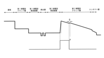
- 1 is a graph showing an example of the Al composition in a nitride semiconductor device according to an embodiment of the present disclosure.
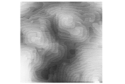
- 4 is an AFM photograph showing the structure of the upper surface of a second conductivity type cladding layer of a nitride semiconductor device according to an embodiment of the present disclosure.
- 4 is an SEM photograph showing the structure of the upper surface of a second conductivity type cladding layer of a nitride semiconductor device according to an embodiment of the present disclosure.
- 1 is an AFM photograph showing a structure of an upper surface of a second conductivity type cladding layer of a conventional nitride semiconductor device.
- 1 is a schematic plan view showing a configuration example of a nitride semiconductor device according to an embodiment of the present disclosure.
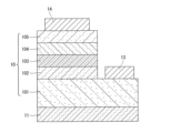
- 1 is a schematic cross-sectional view showing a configuration example of a nitride semiconductor device according to an embodiment of the present disclosure.
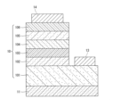
- 1 is a schematic cross-sectional view showing a configuration example of a nitride semiconductor device according to an embodiment of the present disclosure.
- 1 is a schematic cross-sectional view showing a configuration example of a nitride semiconductor device according to an embodiment of the present disclosure.
- the nitride semiconductor device according to this embodiment is, for example, a laser diode.
- the laser diode includes a nitride semiconductor substrate containing Al, and a semiconductor laminate disposed on the nitride semiconductor substrate.
- the semiconductor laminate includes a first-conductivity-type cladding layer containing a first-conductivity-type nitride semiconductor, a first-conductivity-type waveguide layer disposed on the first-conductivity-type cladding layer, a light-emitting layer formed of a nitride semiconductor containing one or more quantum wells and disposed on the first-conductivity-type waveguide layer, a second-conductivity-type waveguide layer disposed on the light-emitting layer, and a second-conductivity-type cladding layer formed of a nitride semiconductor containing Al and disposed on the second-conductivity-type waveguide layer.
- the deviation ⁇ from the uniformity of the alloy in the surface direction of the second-conductivity-type waveguide layer is 130 meV or more
- the nitride semiconductor substrate (hereinafter, sometimes referred to as substrate) includes a nitride semiconductor containing Al.
- the nitride semiconductor containing Al is, for example, AlN. That is, the substrate is preferably an AlN single crystal substrate.
- the nitride semiconductor containing Al is not limited to AlN, and may be, for example, AlGaN.
- the substrate is a nitride semiconductor single crystal substrate such as AlN or AlGaN
- the difference in lattice constant with the nitride semiconductor layer formed on the substrate becomes small, and the nitride semiconductor layer is grown in a lattice-matched system, thereby reducing threading dislocations.
- the threading dislocation density of the substrate is preferably 5 ⁇ 10 4 cm ⁇ 2 or less.
- the threading dislocation density is more preferably 1 ⁇ 10 3 cm ⁇ 2 or more and 1 ⁇ 10 4 cm ⁇ 2 or less.
- the substrate may be formed on a substrate of a different type so long as it contains a nitride semiconductor containing Al.
- AlN may be grown on a sapphire (Al 2 O 3 ) substrate.
- the layer mainly contains a nitride semiconductor means that the layer mainly contains a nitride semiconductor, but this expression also includes cases where other elements are included. Specifically, this expression also includes cases where the composition of this layer is slightly changed by adding a small amount of an element other than a nitride semiconductor (for example, a few percent or less of elements such as Ga (when Ga is not the main element), In, As, P, or Sb). In expressions regarding the composition of other layers, the wording "including” has a similar meaning. Furthermore, the small amount of elements contained is not limited to the above.
- the substrate preferably has a layer thickness of 100 ⁇ m or more and 600 ⁇ m or less.
- the surface orientation may be c-plane (0001), a-plane (11-20), m-plane (10-10), etc., with a c-plane (0001) substrate being more preferable.
- it may be formed on a surface inclined at some angle (for example, -4° to 4°, preferably -0.4° to 0.4°) from the normal direction of the c-plane (0001), but is not limited to this.
- a buffer layer may be formed on the substrate, i.e., between the substrate and the first conductive type cladding layer.
- the buffer layer is preferably formed on the entire surface of the substrate.
- a nitride semiconductor layer having small lattice constant differences and thermal expansion coefficient differences and few defects is formed on the buffer layer.
- the buffer layer is preferably a nitride semiconductor layer containing Al, and is formed of, for example, a nitride semiconductor such as AlN, AlGaN, etc.
- the buffer layer may also contain impurities such as C, Si, Fe, Mg, etc.
- the buffer layer has a thickness of, for example, several micrometers. Specifically, the thickness of the buffer layer is preferably greater than 10 nm and less than 10 ⁇ m. If the buffer layer is greater than 10 nm, the crystallinity of the nitride semiconductor such as AlN is increased. Also, if the buffer layer is less than 10 ⁇ m thick, cracks are less likely to occur in the buffer layer formed by crystal growth over the entire surface of the wafer.
- the first-conductivity-type cladding layer is formed on a substrate.
- the word “on” in the expression “the first-conductivity-type cladding layer is formed on a substrate” means that the first-conductivity-type cladding layer is formed on one side of the substrate.
- the above expression also includes a case where another layer exists between the substrate and the first-conductivity-type cladding layer.
- the word “on” has the same meaning in other relationships between layers.
- the expression “the second-conductivity-type cladding layer is formed on the first-conductivity-type waveguide layer described later with an electron blocking layer interposed therebetween is also included in the expression.
- the terms “first conductivity type” and “second conductivity type” refer to semiconductors exhibiting different conductivity types, and for example, when one is n-type conductivity, the other is p-type conductivity.
- the first conductive cladding layer is a layer of a nitride semiconductor containing Al and Ga.
- the first conductive cladding layer is formed of, for example, Al a Ga (1-a) N (0 ⁇ a ⁇ 1). This makes it possible to enhance the crystallinity of the light emitting layer and improve the light emitting efficiency when a material corresponding to the band gap energy of the deep ultraviolet region is formed as the light emitting layer.
- the nitride semiconductor constituting the first conductive cladding layer is preferably a mixed crystal of AlN and GaN.
- the first conductive cladding layer is formed of Al a Ga (1-a) N (0.65 ⁇ a ⁇ 0.9).
- the first conductivity type cladding layer may be a graded layer in which the Al composition increases with increasing distance from the substrate for the purpose of controlling the longitudinal conductivity, etc.
- the above-mentioned limitation on the Al composition may be the Al composition obtained by averaging the Al composition at positions in the first conductivity type cladding layer in the thickness direction over the thickness of the first conductivity type cladding layer.
- the first conductivity type cladding layer is an n-type conductive semiconductor layer, it may contain impurities such as P, As, Sb, and other Group V elements other than N, C, H, F, O, Mg, Si, etc., but the types of impurity elements are not limited to these.
- the impurity contained in the first conductivity type cladding layer is preferably Si, and the impurity concentration is preferably 5 ⁇ 10 18 cm -3 or more and 5 ⁇ 10 19 cm -3 or more.
- the resistivity of the first conductivity type cladding layer is preferably 1 ⁇ 10 ⁇ 3 ⁇ cm or more and 5 ⁇ 10 ⁇ 3 ⁇ cm or less, which allows efficient carrier injection.
- the first conductivity type cladding layer preferably has a layer thickness of 250 nm or more and 800 nm or less, and more preferably has a layer thickness of 300 nm or more and 450 nm or less.
- the light emitting layer is a layer of a nitride semiconductor containing Al and Ga.
- the nitride semiconductor contained in the light emitting layer is preferably a mixed crystal of, for example, AlN or GaN, and is formed, for example, of Al b Ga (1-b) N (0 ⁇ b ⁇ 1).
- the light emitting layer may contain impurities such as Group V elements other than N, such as P, As, Sb, and C, H, F, O, Mg, and Si, but the types of impurity elements are not limited to these.
- the light-emitting layer may have either a multiple quantum well structure or a single quantum well structure.
- the number of quantum well structures is preferably between 1 and 5.
- ⁇ which indirectly represents the potential fluctuation of the nitride semiconductor layer, is preferably 130 meV or more and 350 meV or less.
- the nitride semiconductor layer represented by such ⁇ may be not only the light emitting layer but also a first conductivity type waveguide layer or a second conductivity type waveguide layer described later.
- ⁇ of the light emitting layer, the first conductivity type waveguide layer, or the second conductivity type waveguide layer is 130 meV or more and 350 meV or less, recombination of localized carriers occurs efficiently, and the light emission efficiency can be improved.
- the “potential fluctuation of the nitride semiconductor layer” is an index for specifying the distribution state of Ga in the surface direction of the nitride semiconductor layer
- “ ⁇ indirectly expressing the potential fluctuation” is an index showing the deviation from the uniformity of the alloy in the surface direction of the nitride semiconductor layer.
- the possible values of the half-width of the emission spectrum also differ depending on the Al composition of the nitride semiconductor. Therefore, the potential fluctuation of the nitride semiconductor layer is evaluated using ⁇ , which expresses the deviation from the half-width of the emission spectrum in a uniform state at each Al composition.
- the thickness of the region where the Al concentration profile changes gradually at the interface between the well layer and the barrier layer in the light-emitting layer is preferably 0.3 nm or more and 0.6 nm or less. This improves carrier confinement and increases the emission intensity.
- the laser diode of this embodiment may include waveguide layers formed above and below the light emitting layer so as to sandwich the light emitting layer and having the effect of confining light emitted from the light emitting layer within the light emitting layer.
- the waveguide layers are preferably composed of two layers, a first conductive type waveguide layer disposed between the first conductive type cladding layer and the light emitting layer, and a second conductive type waveguide layer disposed between the second conductive type cladding layer and the light emitting layer.
- the laser diode of this embodiment may include, for example, a first-conductivity-type waveguide layer disposed between the first-conductivity-type cladding layer and the light-emitting layer to confine light in the light-emitting layer, and a second-conductivity-type waveguide layer disposed between the second-conductivity-type cladding layer and the light-emitting layer to confine light in the light-emitting layer.
- the waveguide layer is preferably a nitride semiconductor containing Al and Ga having a band gap with a higher energy than the light emitting layer.
- the waveguide layer preferably has an Al composition and a film thickness that increase the electric field intensity distribution of light present in the device and the overlap of the light emitting layer.
- the light emitting layer is Al b Ga (1-b) N (0 ⁇ b ⁇ 1) and the waveguide layer is Al c Ga (1-c) N (0 ⁇ c ⁇ 1), it is more preferable that b ⁇ c and c ⁇ b+0.05.
- the total thickness of the waveguide layers is preferably 70 nm or more and 150 nm or less.
- the waveguide layer may contain impurities such as P, As, Sb, and other Group V elements other than N, C, H, F, O, Mg, Si, etc., but the types of impurity elements are not limited to these.
- the impurity contained in the first conductivity type waveguide layer is preferably Si, and the impurity concentration is preferably 5 ⁇ 10 18 cm -3 or more and 5 ⁇ 10 19 cm -3 or less.
- the Al composition of each of the first conductivity type waveguide layer and the second conductivity type waveguide layer is preferably uniform in the film thickness direction, but is not limited to this.
- the Al composition of the second conductivity type waveguide layer may be higher than the Al composition of the first conductivity type waveguide layer.
- the film thickness of the second conductivity type waveguide layer may be thicker than the film thickness of the first waveguide.
- the second conductivity type cladding layer is formed on the light emitting layer and is a nitride semiconductor layer containing Al and Ga having second conductivity type conductivity.
- the second conductivity type cladding layer is formed of, for example, Al d Ga (1-d) N (0.1 ⁇ d ⁇ 1).
- the second conductivity type cladding layer is formed on the second conductivity type waveguide layer. This allows the second conductivity type cladding layer to easily lattice match with the light emitting layer or the waveguide layer, and makes it possible to suppress threading dislocation density.
- the second conductivity type cladding layer is not particularly limited as long as it has sufficient conductivity to inject carriers (electrons or holes) into the light-emitting layer and can increase the overlap between the electric field strength distribution of the optical mode present in the device and the light-emitting layer (i.e., increase the light confinement).
- the second conductivity type cladding layer may be, for example, p-type AlGaN doped with Mg.
- the second conductivity type cladding layer may also contain impurities such as P, As, Sb, and other group V elements other than N, C, H, F, O, Mg, and Si, but the types of impurity elements are not limited to these.
- the second conductivity type cladding layer is a compositionally graded layer formed of Al d Ga (1-d) N (0.1 ⁇ d ⁇ 1) in which the Al composition d decreases with increasing distance from the substrate as a whole, while in a portion of the second conductivity type cladding layer, the Al composition d increases with increasing distance from the substrate.
- the second conductive type cladding layer preferably has a composition gradient in which the Al composition d decreases in the range of 1 to 0.7 with increasing distance from the nitride semiconductor substrate side.
- the profile (gradient) of the Al composition d in the second conductive type cladding layer may decrease continuously or may decrease intermittently.
- the second conductive type cladding layer includes a part in which the Al composition d is the same (constant in the film thickness direction).
- the second conductive type cladding layer may include a part in which the Al composition d does not decrease (a part in which the Al composition d is constant or increases) in the direction away from the substrate.
- the thickness of the second conductive cladding layer is preferably 500 nm or less from the viewpoint of lattice matching. Moreover, from the viewpoint of optical confinement, it is more preferable that the thickness is 250 nm or more and 500 nm or less.
- the second-conductivity-type cladding layer has a composition gradient such that the Al composition d decreases with increasing distance from the substrate.
- a portion of the second-conductivity-type cladding layer is doped with impurities such as carbon or oxygen.
- the impurities are also doped into an interface gradient portion on the second-conductivity-type waveguide layer where the Al composition increases, for example, so that the concentration profile increases discontinuously at the start point of the composition gradient layer (the interface on the second-conductivity-type waveguide layer side).
- the second conductivity type cladding layer is often formed of a nitride semiconductor that is doped with almost no impurities for the purpose of suppressing the diffusion of impurities and improving injection efficiency, etc.
- impurities for the purpose of suppressing the diffusion of impurities and improving injection efficiency, etc.
- the second conductive type cladding layer has at least one region where the concentration profile of carbon or oxygen contained in the second conductive type cladding layer changes discontinuously as it moves away from the substrate.
- the impurity concentration profile has a region that is convex in the direction of increasing concentration.
- the concentration profile of carbon or oxygen in the second conductive type cladding layer slopes at a steep slope, improving the effect of improving the injection efficiency of carriers into the light-emitting layer, and the second conductive type cladding layer can achieve both the effect of suppressing deterioration of the second conductive type cladding layer and the effect of improving the injection efficiency of carriers into the light-emitting layer.
- the impurity concentration profile has a region that is convex in the direction in which the concentration increases, this is disadvantageous in terms of the efficiency of carrier injection into the light-emitting layer; however, depending on the thickness of the second cladding layer, providing a region in which the carbon or oxygen concentration profile has a steep slope can be advantageous overall in terms of the efficiency of carrier injection into the light-emitting layer.
- a region in which the concentration profile discontinuously decreases with increasing distance from the substrate (nitride semiconductor substrate) at at least one point refers to a region in which the impurity concentration in a certain region (the impurity concentration measured at a measurement point in that region) differs by a factor of two or more from the surrounding impurity concentration (the impurity concentration measured at a measurement point in an adjacent region).
- the impurity concentration profile changes abruptly.
- the second conductivity type cladding layer has a region P where the impurity concentration profile decreases discontinuously.
- the region P where the concentration profile decreases discontinuously is preferably present in a region of 1 nm to 110 nm from the substrate side of the second conductivity type cladding layer, and more preferably in a region of 5 nm to 110 nm. This makes it possible to suppress deterioration of the second conductivity type cladding layer without impeding the improvement of the efficiency of carrier injection into the light-emitting layer.
- the region of the second conductive type cladding layer closer to the substrate than the region P where the impurity concentration profile discontinuously decreases is preferably made of Al e Ga (1-e) N (0.8 ⁇ e ⁇ 1.0), which makes it possible to suppress deterioration of the second conductive type cladding layer without impeding the improvement of the efficiency of carrier injection into the light emitting layer.
- the carbon concentration in a region closer to the substrate than the region P where the impurity concentration profile decreases discontinuously is preferably 1 ⁇ 10 17 cm ⁇ 3 or more and 1 ⁇ 10 18 cm ⁇ 3 or less.
- the oxygen concentration in a region closer to the substrate than the region P where the impurity concentration profile decreases discontinuously is preferably 1 ⁇ 10 17 cm ⁇ 3 or more and 1 ⁇ 10 18 cm ⁇ 3 or less.
- the second conductivity type cladding layer has the composition discontinuous region Q, and the laser diode can achieve both the effect of suppressing deterioration of the second conductivity type cladding layer and the effect of improving the efficiency of carrier injection into the light emitting layer.
- Composition discontinuous region Q is preferably present in a region of 1 nm or more and 110 nm or less from the nitride semiconductor substrate side of the second conductivity type cladding layer, and more preferably in a region of 5 nm or more and 110 nm or less. That is, the start point of composition discontinuous region Q preferably coincides with the start point of region P.
- the composition discontinuous region Q has a composition gradient in which the Al composition d increases from 0.002 to 0.05 with increasing distance from the substrate.
- a layer that is effective in suppressing deterioration of the second conductive type cladding layer and a layer that is effective in improving the injection efficiency of carriers into the light emitting layer are formed. Therefore, it is possible to more effectively achieve both the effect of suppressing deterioration of the second conductive type cladding layer in the laser diode and the effect of improving the injection efficiency of carriers into the light emitting layer.
- the interface of the second conductivity type cladding layer on the substrate side preferably contains hydrogen at a concentration of 1 ⁇ 10 17 cm ⁇ 3 or more and 5 ⁇ 10 19 cm ⁇ 3 or less.
- At least a portion of the second conductivity type cladding layer preferably contains hydrogen at a higher concentration than other regions of the second conductivity type cladding layer.
- the second conductivity type cladding layer of the laser diode of this embodiment includes a region (the portion) partially containing a high concentration of hydrogen. This allows the laser diode to compensate for point defects and achieve both the effect of suppressing deterioration of the second conductivity type cladding layer and the effect of improving the efficiency of carrier injection into the light emitting layer.
- the region containing hydrogen at a higher concentration than other regions of the second conductive type cladding layer is preferably a region of 1 nm or more and 110 nm or less from the substrate side of the second conductive type cladding layer, and more preferably a region of 5 nm or more and 110 nm or less, which makes it possible to compensate for point defects and suppress deterioration of the second conductive type cladding layer without impeding the improvement of the efficiency of carrier injection into the light emitting layer.
- the half width of the hydrogen concentration profile in the region containing hydrogen at a higher concentration than other regions of the second conductivity type cladding layer is preferably 5 nm to 10 nm, which makes it possible to effectively compensate for point defects and improve the efficiency of carrier injection into the light emitting layer.
- the interface of the second conductivity type cladding layer on the substrate side may contain silicon at a concentration of 1 ⁇ 10 17 cm -3 or more and 5 ⁇ 10 19 cm -3 or less. At least a portion of the second conductivity type cladding layer may contain silicon at a higher concentration than other regions of the second conductivity type cladding layer.
- the region containing silicon at a higher concentration than other regions of the second conductivity type cladding layer is preferably a region 1 nm or more and 110 nm or less from the substrate side of the second conductivity type cladding layer, and more preferably a region 5 nm or more and 110 nm or less.
- the surface of the second conductive cladding layer as described above has a spiral step-terrace structure having terraces and steps other than linear in plan view, as shown in FIG. 2A.
- An example of the spiral step-terrace structure is a hexagonal shape with one side of the outline gradually becoming shorter.
- Other examples of the spiral step-terrace structure are a circular shape with a gradually shortened radius, or a mixed shape of a hexagon and a straight line with a gradually shortened side length.
- FIG. 3 shows a step-terrace structure having linear terraces and steps in plan view. This makes it possible to better achieve both the effect of suppressing deterioration of the second conductive cladding layer in the laser diode and the effect of improving the injection efficiency of carriers into the light emitting layer.
- FIG. 2A is an atomic force microscope (AFM) photograph showing the spiral step-terrace structure
- FIG. 2B is a scanning electron microscope (SEM) photograph showing the circular step-terrace structure.
- the spiral step-terrace structure provides a higher effect of improving the luminous efficiency of the second conductive type cladding layer. This is believed to be because Ga is segregated during the growth of the film with the spiral step-terrace structure, improving the current injection efficiency.
- the height of the spiral step-terrace structure is preferably 0.2 nm or more and 0.4 nm or less.
- the distribution density of the spiral step-terrace structure is preferably 1 ⁇ 10 7 cm ⁇ 2 or more and 5 ⁇ 10 8 cm ⁇ 2 or less. This makes it possible to obtain a further improved effect of suppressing deterioration of the second conductivity type cladding layer and to improve the current injection efficiency.
- the spiral step-terrace structure when a nitride semiconductor layer having a spiral step-terrace structure is formed and then a nitride semiconductor layer is formed by a conventional method to form a second conductive cladding layer, the spiral step-terrace structure also appears on the surface of the second conductive cladding layer. Therefore, by observing the surface shape of the second conductive cladding layer, the spiral step-terrace structure on the surface of the second conductive cladding layer can be confirmed. In addition, when a second conductive contact layer, which will be described later, is formed on the second conductive cladding layer, the spiral step-terrace structure does not appear on the surface of the second conductive contact layer.
- the laser diode according to this embodiment may have an interface slope portion on the light emitting layer (second conductivity type waveguide) that contains Al g Ga (1-g) N (0.1 ⁇ g ⁇ 1) and the Al composition g increases with increasing distance from the nitride semiconductor substrate.
- the interface slope portion As in this embodiment, the electric field is relaxed, and the degradation suppression effect is improved.
- the thickness of the inclined interface portion is preferably 2 nm to 5 nm, more preferably 2 nm to 3 nm, in which case the degradation suppression effect is further improved.
- the semiconductor laminate of the laser diode of this embodiment may further include a second-conductivity-type contact layer disposed on the second-conductivity-type cladding layer.
- the nitride semiconductor constituting the second-conductivity-type contact layer is preferably formed of, for example, GaN, AlN, or InN, or a mixed crystal containing these, and more preferably is a nitride semiconductor containing GaN.
- the second conductive type contact layer may contain impurities such as P, As, Sb, and other V group elements other than N, C, H, F, O, Mg, Si, and Be.
- the impurity contained in the second conductive type contact layer is preferably Mg.
- the concentration of Mg is preferably 8 ⁇ 10 19 cm -3 or more and 5 ⁇ 10 21 cm -3 or less, and more preferably 5 ⁇ 10 20 cm -3 or more and 5 ⁇ 10 21 cm -3 or less.
- the thickness of the second conductive contact layer is preferably 1 nm or more and 20 nm or less. The thinner the second conductive contact layer is, the more efficient the carrier injection into the light-emitting layer is, and the thicker the layer is, the more efficient the carrier injection is.
- the semiconductor laminate of the laser diode of this embodiment may further include an electron blocking layer above the light emitting layer, the electron blocking layer having a band gap larger than that of the light emitting layer.
- the electron blocking layer may be provided, for example, on the light emitting layer, or may be provided inside the second conductive type waveguide layer, between the second conductive type waveguide layer and the light emitting layer, or between the second conductive type waveguide layer and the second conductive type cladding layer.
- the thickness of the electron blocking layer is preferably 30 nm or less, and more preferably 20 nm or less, so that carriers (holes) can easily quantum-transport through the electron blocking layer.
- the laser diode can emit light or oscillate by injecting a current through a second electrode disposed on the second conductive type cladding layer and a first electrode disposed on the first conductive type cladding layer, where the first electrode is formed so as to be in electrical contact with the first conductive type cladding layer, and the second electrode is formed so as to be in electrical contact with the second conductive type cladding layer.
- the first electrode can be disposed, for example, on the back side of the substrate.
- the first electrode is also disposed on the first conductivity type cladding layer that is exposed by removing the layers above the first conductivity type cladding layer of the semiconductor laminate by, for example, chemical etching or dry etching.
- the first electrode is disposed on a region of the first conductivity type cladding layer that does not form a mesa structure.
- the first electrode is formed of a metal such as Al, Ti, Zr, Hf, V, Nb, Ta, Cr, Mo, W, Co, Rh, Ir, Ni, Pd, Pt, Cu, Ag, Au, Zr, or a mixed crystal thereof, or a conductive oxide such as ITO or Ga2O3 .
- the first electrode is formed of a metal such as Ni, Au, Pt, Ag, Rh, Pd, Pt, Cu, Al, Ti, Zr, Hf, V, Nb, Ta, Cr, Mo, W, Co, Ir, Zr, or a mixed crystal thereof, or a conductive oxide such as ITO or Ga2O3 .
- the second electrode is formed of a metal such as Al, Ti, Zr, Hf, V, Nb, Ta, Cr, Mo, W, Co, Rh, Ir, Ni, Pd, Pt, Cu, Ag, Au, Zr, or a mixed crystal thereof, or a conductive oxide such as ITO or Ga2O3 .
- the second electrode is formed of a metal such as Ni, Au, Pt, Ag, Rh, Pd, Pt, Cu, Al, Ti, Zr, Hf, V, Nb, Ta, Cr, Mo, W, Co, Ir, Zr, or a mixed crystal thereof, or a conductive oxide such as ITO or Ga2O3 .
- the arrangement area and shape of the first electrode and the second electrode are not limited as long as electrical contact is obtained with the first conductivity type clad layer and the second conductivity type clad layer (or the second conductivity type contact layer if a second conductivity type contact layer is provided).
- the laser diode which is the nitride semiconductor device of this embodiment, can be manufactured by singulating a nitride semiconductor stack manufactured through a process of forming each nitride semiconductor layer on a substrate.
- a method for manufacturing a nitride semiconductor stack and a method for manufacturing a laser diode as an example of a method for manufacturing a nitride semiconductor device will be described.
- the substrate is formed by a general substrate growth method such as a vapor phase growth method, such as a sublimation method or a hydride vapor phase epitaxy (HVPE) method, or a liquid phase growth method.
- a general substrate growth method such as a vapor phase growth method, such as a sublimation method or a hydride vapor phase epitaxy (HVPE) method, or a liquid phase growth method.
- Each layer of the semiconductor laminate layer formed on the substrate can be formed by, for example, a molecular beam epitaxy (MBE) method, a hydride vapor phase epitaxy (HVPE) method, or a metal organic chemical vapor deposition (MOCVD) method.
- MBE molecular beam epitaxy
- HVPE hydride vapor phase epitaxy
- MOCVD metal organic chemical vapor deposition
- the nitride semiconductor layer can be formed using, for example, an Al source containing trimethylaluminum (TMAl), a Ga source containing trimethylgallium (TMGa) or triethylgallium (TEGa), or an N source containing ammonia (NH 3 ).
- a semiconductor laminate layer is formed on the substrate. At this time, an organometallic gas is flowed into the semiconductor laminate layer formation space. First, a first conductivity type cladding layer containing a first conductivity type nitride semiconductor is formed on the substrate.
- a first conductivity type waveguide layer made of a nitride semiconductor such as AlGaN is formed on the first conductivity type cladding layer, and then a light emitting layer is formed from a nitride semiconductor (such as AlGaN) that includes one or more quantum wells.
- a second conductivity type waveguide layer made of a nitride semiconductor such as AlGaN is formed on the light emitting layer.
- the first conductivity type waveguide layer, the light emitting layer and the second conductivity type waveguide layer are preferably formed under conditions that satisfy ⁇ 2Tw+2050 ⁇ Vw ⁇ 2Tw+2350 (850° C. ⁇ Tw ⁇ 970° C.), where Tw is the wafer temperature and Vw is the reactor pressure.
- Tw is the wafer temperature
- Vw is the reactor pressure.
- a second conductivity type cladding layer is formed on the second conductivity type waveguide layer.
- the flow of the metal-organic gas is temporarily stopped to interrupt the growth of the nitride semiconductor layer, and the film formation conditions are changed.
- the flow of the metal organic gas is temporarily stopped again to interrupt the growth of the nitride semiconductor layer and the film formation conditions are changed.
- the wafer temperature is changed to 1030° C. to 1100° C.
- the reactor pressure is changed to 15 mbar to 350 mbar, and the flow of the metalorganic gas is resumed to form the remaining part of the second conductivity type cladding layer.
- the first conductivity type cladding layer, the first conductivity type waveguide layer, the light emitting layer, and the second conductivity type waveguide layer in the above manner, it is possible to increase the recombination rate of carriers and reduce point defects in each layer, thereby suppressing degradation and improving the light emitting efficiency. Furthermore, by setting the wafer temperature when forming a portion of the second conductivity type cladding layer lower than the wafer temperature when forming the remaining portion of the second conductivity type cladding layer, it is possible to form at least one region in which the carbon or oxygen concentration profile in the portion of the second conductivity type cladding layer and the remaining portion of the second conductivity type cladding layer discontinuously decreases with increasing distance from the substrate.
- the portion of the second conductivity type cladding layer can be formed to contain more carbon or oxygen than the remaining portion of the second conductivity type cladding layer. This makes it possible to achieve both suppression of deterioration and improvement of injection efficiency in the second conductivity type cladding layer. Furthermore, by setting the reactor pressure when forming a portion of the second conductivity type cladding layer lower than the reactor pressure when forming the remaining portion of the second conductivity type cladding layer, the portion of the second conductivity type cladding layer can be formed to contain more carbon or oxygen as an impurity compared to the remaining portion of the second conductivity type cladding layer.
- hydrogen and silicon are localized at the interface of the second-conductivity-type cladding layer on the substrate side.
- hydrogen gas (H 2 ) is used as the carrier gas
- hydrogen (H) is likely to be localized in the uppermost layer of the nitride semiconductor layer where the growth is interrupted (for example, the interface between the second-conductivity-type waveguide layer and the second-conductivity-type cladding layer and a part of the second-conductivity-type cladding layer).
- This allows the laser diode to further improve the effect of suppressing deterioration of the second-conductivity-type cladding layer and the effect of improving the efficiency of carrier injection into the light-emitting layer.
- the wafer temperature when forming a portion of the second conductivity type cladding layer is set lower than the wafer temperature when forming the remaining portion of the second conductivity type cladding layer, thereby forming at least one region in which the carbon or oxygen concentration profile in the portion of the second conductivity type cladding layer and the remaining portion of the second conductivity type cladding layer discontinuously decreases with increasing distance from the substrate, but the manufacturing method is not limited to this.
- the flow rate of the organometallic gas may be intentionally changed during the formation of the second conductivity type cladding layer to form a region in which the carbon or oxygen concentration profile discontinuously decreases with increasing distance from the substrate.
- an intermediate layer may be formed between the second conductive cladding layer and the second conductive waveguide layer using a nitride semiconductor such as AlGaN, a second conductive contact layer may be provided on the second conductive cladding layer using a nitride semiconductor including GaN, or an electron blocking layer may be formed above the light emitting layer.
- a nitride semiconductor such as AlGaN
- a second conductive contact layer may be provided on the second conductive cladding layer using a nitride semiconductor including GaN
- an electron blocking layer may be formed above the light emitting layer.
- Laser diodes are manufactured through a process of forming a semiconductor laminate by removing unnecessary portions of each layer of a semiconductor laminate formed on a substrate by etching (mesa structure forming process).
- the unnecessary portions of each layer of the semiconductor laminate can be removed by, for example, inductively coupled plasma (ICP) etching.
- ICP inductively coupled plasma
- unnecessary portions of each layer of the conductor laminate layer are removed by etching, thereby exposing a portion of the first conductivity type cladding layer.
- the laser diode may be manufactured through a process of forming electrodes.
- the electrodes such as the first electrode and the second electrode, may be formed by various methods of evaporating metal by an electron beam deposition (EB) method, such as resistance heating deposition, electron gun deposition, or sputtering, but are not limited to these methods.
- EB electron beam deposition
- Each electrode may be formed as a single layer or may be formed by laminating multiple layers.
- each electrode may be subjected to a heat treatment in an oxygen, nitrogen or air atmosphere after the metal layer is formed.
- the substrate on which the layers have been formed through the above-mentioned steps is divided into individual pieces by dicing to manufacture nitride semiconductor devices (laser diodes).
- a first electrode is formed on the surface of the first conductive cladding layer.
- the second electrode is formed on the top layer (e.g., the second conductive cladding layer) of a mesa structure that is a part of the semiconductor laminate.
- the formed electrode is alloyed by heating with a rapid thermal annealing (RTA) device, which is a heating process using an infrared lamp, or by laser annealing, which is a heating process using a laser pulse, to obtain contact with the semiconductor laminate.
- RTA rapid thermal annealing
- the method of alloying is not particularly limited as long as sufficient contact with the semiconductor laminate can be obtained.
- the carrier injection efficiency can be improved, and the emission intensity can be increased.
- the thickness of each layer constituting the laser diode can be measured by cutting out a predetermined cross section perpendicular to the substrate, observing this cross section with a transmission electron microscope (TEM), and using the length measurement function of the TEM.
- TEM transmission electron microscope
- a measurement method first, a cross section perpendicular to the main surface of the substrate of the laser diode is observed using a TEM.
- the observation width is set to a range of 2 ⁇ m or more in a direction parallel to the main surface of the substrate in a TEM image showing a cross section perpendicular to the main surface of the substrate of the laser diode.
- the concentration of dopants and impurities contained in each layer constituting the laser diode can be measured by secondary ion mass spectrometry (SIMS).
- SIMS secondary ion mass spectrometry
- the concentration of dopants and impurities contained in each layer can be measured by SIMS after processing into a device, the measurement can be performed in a state where the electrodes are removed by chemical etching or physical polishing.
- the concentration of dopants and impurities contained in each layer can also be measured by sputtering from the substrate side where no electrodes are formed.
- the SIMS measurement is performed under the measurement conditions provided by Evans Analytical Group (EAG), Inc.
- a cesium (Cs) ion beam having an energy of 14.5 keV is used for sputtering the sample during the measurement.
- a method for measuring the atomic concentration in each layer constituting a laser diode includes reciprocal space mapping (RSM) using X-ray diffraction (XRD).
- RSM reciprocal space mapping
- XRD X-ray diffraction
- the lattice relaxation rate and Al composition relative to the underlayer can be obtained by analyzing reciprocal space mapping data in the vicinity of a diffraction peak obtained with an asymmetric plane as a diffraction plane.
- the diffraction plane include the (10-15) plane and the (20-24) plane.
- layers and regions that do not provide sufficient reflection intensity by XRD can be measured using X-ray photoelectron spectroscopy (XPS), energy dispersive X-ray spectroscopy (EDX), and electron energy-loss spectroscopy (EELS).
- XPS X-ray photoelectron spectroscopy
- EDX energy dispersive X-ray spectroscopy
- EELS electron energy-loss spectroscopy
- the composition of a sample is analyzed by measuring the energy lost when an electron beam passes through the sample.
- the energy loss spectrum of the intensity of the transmitted electron beam is measured and analyzed for a thin-sectioned sample used in TEM observations.
- the position of the peak that appears at an energy loss of around 20 eV changes depending on the composition of each layer, and the composition can be determined from the peak position.
- the Al composition of each layer is obtained by calculating the average value of the Al composition in an observation width of 200 nm from five points randomly selected from an observation area of 2 ⁇ m or more.
- the EDX measures and analyzes the characteristic X-rays generated by the electron beam in the thin-sectioned sample used in the above-mentioned TEM observation.
- the Al composition of each layer is obtained by calculating the average value of the Al composition in an observation width of 200 nm from five points randomly selected from an observation area of 2 ⁇ m or more.
- XPS depth direction evaluation is possible by performing XPS measurement while performing sputter etching using an ion beam.
- Ar+ is generally used for the ion beam
- other ion species such as Ar cluster ions can be used as long as they can be irradiated with the etching ion gun mounted on the XPS device.
- the XPS peak intensities of Al, Ga, and N are measured and analyzed to obtain the depth direction distribution of the Al composition of each layer.
- the laser diode can be polished at an angle so that a cross section perpendicular to the main surface of the substrate is enlarged and exposed, and the exposed cross section can be measured by XPS.
- the composition of each layer can be measured not only by XPS but also by Auger Electron Spectroscopy (AES). In this case, the composition can be measured by performing Auger Electron Spectroscopy on a cross section exposed by sputter etching or angled polishing. The composition of each layer can also be measured by SEM-EDX measurement of a cross section exposed by angled polishing.
- AES Auger Electron Spectroscopy
- Methods for measuring the surface shape of the second conductivity type cladding layer include a scanning electron microscope (SEM) and an atomic force microscope (AFM). Specifically, the surface of the second conductive type cladding layer is observed using a scanning electron microscope SU9000 manufactured by Hitachi High-Tech Corporation at an accelerating voltage of 30 kV. At this time, the surface shape of the second conductive type cladding layer can be clearly observed by setting the magnification to 10K to 50K. Under these conditions, the number of spiral step-terrace structures contained within the observation range is counted, and the value obtained by dividing the number by the area is taken as the density of the spiral step-terrace structures.
- SEM scanning electron microscope
- AFM atomic force microscope
- the step height of the spiral step-terrace structure on the surface of the second conductive type cladding layer can be measured by AFM. Specifically, the observation is performed using a scanning probe microscope manufactured by Hitachi High-Tech Corporation. When observing with the scanning probe microscope, the AFM mode is used to observe an area of 2 ⁇ m square. The step height can be obtained from the obtained AFM measurement.
- the laser diode according to the present disclosure can be applied to devices in, for example, the medical and life science fields, the environmental field, the industrial and manufacturing fields, the household appliances field, the agricultural field, and other fields.
- the laser diode can be applied to a drug or chemical synthesis/decomposition device, a liquid/gas/solid (container, food, medical equipment, etc.) sterilization device, a semiconductor cleaning device, etc., a surface modification device for film, glass, metal, etc., an exposure device for manufacturing semiconductors, FPD (Flat Panel Display), PCB (Printed Wiring Board), and other electronic products, a printing/coating device, an adhesive/sealing device, a transfer/molding device for film, pattern, mockup, etc., and a measurement/inspection device for banknotes, wounds, blood, chemical substances, etc.
- a drug or chemical synthesis/decomposition device e.g., a liquid/gas/solid (container, food, medical equipment, etc.) sterilization device, a semiconductor cleaning device, etc., a surface modification device for film, glass, metal, etc., an exposure device for manufacturing semiconductors, FPD (Flat Panel Display), PCB (Printed Wiring Board), and
- liquid sterilization equipment examples include, but are not limited to, automatic ice makers, ice trays and ice storage containers in refrigerators, water tanks for ice makers, freezers, ice makers, humidifiers, dehumidifiers, cold water tanks, hot water tanks and flow piping for water servers, freestanding water purifiers, portable water purifiers, water supply units, hot water heaters, wastewater treatment equipment, garbage disposers, toilet drain traps, washing machines, dialysis water sterilization modules, peritoneal dialysis connector sterilizers, disaster water storage systems, etc.
- gas sterilization devices include, but are not limited to, air purifiers, air conditioners, ceiling fans, floor or bedding vacuum cleaners, futon dryers, shoe dryers, washing machines, clothes dryers, indoor germicidal lamps, storage ventilation systems, shoe boxes, chests of drawers, etc.
- solid sterilization equipment include, but are not limited to, vacuum packing machines, belt conveyors, hand tool sterilization equipment for medical/dental use, barber shops/beauty salons, toothbrushes, toothbrush holders, chopstick cases, cosmetic pouches, drain covers, toilet spot cleaners, toilet lids, etc.
- the nitride semiconductor device according to this embodiment is, for example, a light emitting device.
- a case where the nitride semiconductor device is a light emitting device will be described.
- the light-emitting device includes a nitride semiconductor substrate containing Al, and a semiconductor laminate portion disposed on the substrate.
- the semiconductor laminate portion includes a first-conductivity-type cladding layer containing a first-conductivity-type nitride semiconductor, a light-emitting layer disposed on the first-conductivity-type cladding layer and formed of a nitride semiconductor including one or more quantum wells, and a second-conductivity-type cladding layer disposed on the light-emitting layer and formed of a second-conductivity-type nitride semiconductor.
- the deviation ⁇ from the uniformity of the alloy in the surface direction of the second-conductivity-type waveguide layer is 130 meV or more and 350 meV or less.
- the light emitting device of this embodiment differs from the laser diode of the first embodiment in that it does not include a first conductive type waveguide layer and a second conductive type waveguide layer.
- the second conductive type cladding layer may be used as a barrier layer.
- the light emitting device of this embodiment has a different configuration from the first conductive cladding layer of the laser diode of the first embodiment, so the first conductive cladding layer and the second conductive cladding layer of the light emitting device will be described in detail below. Note that the layers other than the first conductive type cladding layer, that is, the nitride semiconductor substrate, the buffer layer, and the light emitting layer, are similar to the layers described in the first embodiment, and therefore description thereof will be omitted.
- the first conductive type cladding layer is a nitride semiconductor layer containing Al and Ga.
- the first conductive type cladding layer is formed of, for example, Al a Ga (1-a) N (0 ⁇ a ⁇ 1), and is preferably formed of, for example, Al a Ga (1-a) N (0.7 ⁇ a ⁇ 1).
- the first conductivity type cladding layer is preferably made of an n-type semiconductor.
- the thickness T0 of the first conductivity type cladding layer is not less than 3300 ⁇ a ⁇ 2100 nm and not more than 15700 ⁇ a ⁇ 10100 nm (a is the proportion of Al atoms when the total number of group III atoms in the nitride semiconductor constituting the first conductivity type cladding layer is taken as 1).
- the resistivity of the first conductivity type cladding layer is preferably not less than 1 ⁇ 10 ⁇ 3 ⁇ cm and not more than 5 ⁇ 10 ⁇ 3 ⁇ cm. The rest of the configuration is similar to that of the first conductivity type cladding layer described in the first embodiment.
- ⁇ Second Conductive Type Cladding Layer> In the light-emitting device, instead of a second-conductivity-type cladding layer with a graded Al composition, an electron block layer with a constant Al composition is provided on the light-emitting layer, and a second-conductivity-type contact layer with a graded Al composition is provided on the electron block layer.
- the electron block layer and the second-conductivity-type contact layer with a graded Al composition together function as a cladding layer.
- the electron block layer and the second conductive type contact layer are regarded as a second conductive type cladding layer, the inflow of the metalorganic gas is temporarily stopped before the growth of the electron block layer to interrupt the growth of the nitride semiconductor layer, and only a part of the electron block layer is grown at a low temperature.
- a light emitting device is obtained in which the concentration profile of carbon or oxygen decreases discontinuously, hydrogen is localized at the interface of the electron block layer on the light emitting layer side, and more impurities are contained in the electron block layer than in the past.
- the metal-organic gas after the growth of the electron blocking layer and before the growth of the second conductivity type contact layer to interrupt the growth of the nitride semiconductor layer, it becomes possible to impart hydrogen at a higher concentration to a region of the second conductivity type cladding layer (the layer combining the electron blocking layer and the second conductivity type contact layer) that is away from the nitride semiconductor substrate side by the thickness of the electron blocking layer than to other regions.
- the thickness of the electron blocking layer is preferably 10 nm or more and 15 nm or less.
- the region in which the concentration profile of carbon or oxygen contained in the electron blocking layer decreases discontinuously is preferably present in a region of 10 nm or more and 15 nm or less from the substrate side of the electron blocking layer.
- the light-emitting element according to this embodiment does not include a first conductivity type waveguide layer and a second conductivity type waveguide layer. This makes it difficult to evaluate ⁇ , which indirectly represents potential fluctuations. This is because, when attempting to evaluate ⁇ , which indirectly represents potential fluctuations, the quantized light-emitting layer is excited and a correct result cannot be obtained.
- a nitride semiconductor layer under the same conditions as in the first embodiment, it is possible to form a nitride semiconductor layer having ⁇ , which indirectly represents a similar potential fluctuation.
- Nitride semiconductor devices of the present embodiment will now be described in more detail with reference to Figures 4 to 7.
- the detailed configurations of the layers in the following examples are as described above.
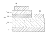
- FIG. 4 is a schematic cross-sectional view of a laser diode 1 as a first example.
- the laser diode 1 includes a substrate 11, a semiconductor laminate 10 disposed on the substrate, a first electrode 13, and a second electrode 14.
- the semiconductor laminate 10 includes a first conductivity type cladding layer 101 having an n-type conductivity, a first conductivity type waveguide layer 102, a light emitting layer 103, a second conductivity type waveguide layer 104, and a second conductivity type cladding layer 105 having a p-type conductivity.
- FIG. 5 is a schematic cross-sectional view of a laser diode 2 as a second example.
- the laser diode 2 includes a substrate 11, a buffer layer 12, a semiconductor laminate 10 disposed on the substrate 11 (buffer layer 12), a first electrode 13, and a second electrode 14.
- the semiconductor laminate 10 includes a first conductivity type cladding layer 101 having an n-type conductivity, a first conductivity type waveguide layer 102, a light emitting layer 103, a second conductivity type waveguide layer 104, and a second conductivity type cladding layer 105 having a p-type conductivity. That is, the laser diode 2 differs from the laser diode 1 in that the laser diode 2 includes a buffer layer 12 .
- FIG. 6 is a schematic cross-sectional view of a laser diode 3 as a third example.
- the laser diode 3 includes a substrate 11, a buffer layer 12, a semiconductor laminate 10 disposed on the substrate, a first electrode 13, and a second electrode 14.
- the semiconductor laminate 10 includes a first conductivity type cladding layer 101 having an n-type conductivity type, a first conductivity type waveguide layer 102, a light emitting layer 103, a second conductivity type waveguide layer 104, a second conductivity type cladding layer 105 having a p-type conductivity type, and a contact layer 106.
- the laser diode 3 differs from the laser diode 1 in that the laser diode 3 includes a contact layer 106 .
- the laser diode of the present disclosure may have a configuration including the buffer layer 12 described in the second example and the contact layer 106 described in the third example.
- FIG. 7 is a schematic cross-sectional view of the light-emitting element 4, which is the first example.
- the light-emitting element 4 includes a substrate 11, a semiconductor laminate 10 disposed on the substrate, a first electrode 13, and a second electrode 14.
- the semiconductor laminate 10 includes a first conductive type cladding layer 101 having an n-type conductivity, a light-emitting layer 103, and a second conductive type cladding layer 105 having a p-type conductivity.
- an electron block layer and a second conductive type contact layer are provided to play the role of the second conductive type cladding layer 105.
- the light-emitting element 4 differs from the laser diode 1 in that it does not include the first-conductivity-type waveguide layer 102 and the second-conductivity-type waveguide layer 104.
- the light-emitting element 4 also differs from the laser diode 1 in that it is provided with an electron blocking layer and a second-conductivity-type contact layer that serves as the second-conductivity-type cladding layer 105.
- the light-emitting element of the present disclosure may have a configuration including the buffer layer 12 described in the second example.
- a nitride semiconductor device includes a nitride semiconductor substrate containing Al, and a semiconductor laminate disposed on the nitride semiconductor substrate.
- the semiconductor laminate includes a first-conductivity-type clad layer containing a first-conductivity-type nitride semiconductor, a first-conductivity-type waveguide layer disposed on the first-conductivity-type clad layer, a light-emitting layer formed of a nitride semiconductor containing one or more quantum wells and disposed on the first-conductivity-type waveguide layer, a second-conductivity-type waveguide layer disposed on the light-emitting layer, and a second-conductivity-type clad layer formed of a second-conductivity-type nitride semiconductor containing Al and disposed on the second-conductivity-type waveguide layer.
- the deviation ⁇ from the uniformity of the alloy in the surface direction of the second-conductivity-type waveguide layer is 130 meV or
- the thickness of the region where the Al concentration profile increases steeply at the interface between the quantum well layer and the barrier layer of the light emitting layer is preferably 0.3 nm or more and 0.6 nm or less. This makes it possible to suppress deterioration of the second conductivity type cladding layer without impeding the improvement of the efficiency of carrier injection into the light emitting layer.
- a method for manufacturing a nitride semiconductor laminate according to the present disclosure includes forming a first conductivity type cladding layer containing a first conductivity type nitride semiconductor on a nitride semiconductor substrate containing Al, forming a first conductivity type waveguide layer, a light emitting layer containing a nitride semiconductor including one or more quantum wells, and a second conductivity type waveguide layer on the first conductivity type cladding layer under conditions of a wafer temperature of 850° C. or more and 970° C.
- the wafer temperature Tw and the reactor pressure Vw during formation of the light emitting layer satisfy ⁇ 2Tw+2050 ⁇ Vw ⁇ 2Tw+2350 (850° C. ⁇ Tw ⁇ 970° C.). This reduces point defects in the light-emitting layer, and improves the light-emitting efficiency.
- a portion of the second conductivity type cladding layer under conditions of a wafer temperature of not less than 900° C. and not more than 1000° C. and a reactor pressure of not less than 15 mbar and not more than 350 mbar, and to form the remaining portion of the second conductivity type cladding layer under conditions of a wafer temperature of not less than 1030° C. and not more than 1100° C. and a reactor pressure of not less than 15 mbar and not more than 350 mbar.
- the reactor pressure during the formation of a portion of the second conductivity type cladding layer is preferably 15 mbar or more and 100 mbar or less. This allows a portion of the second conductivity type cladding layer to be formed so as to contain more carbon or oxygen than the remaining portion of the second conductivity type cladding layer, thereby further improving the deterioration suppression effect and injection efficiency in the second conductivity type cladding layer.
- a nitride semiconductor stack it is preferable to flow an organometallic gas during the formation of the first conductivity type cladding layer, the light emitting layer, and the second conductivity type cladding layer, to temporarily stop the flow of the organometallic gas after the light emitting layer is formed and before forming a portion of the second conductivity type cladding layer, and to temporarily stop the flow of the organometallic gas after the portion of the second conductivity type cladding layer is formed and before forming the remaining portion of the second conductivity type cladding layer.
- the laser diode of the present disclosure will be described below with reference to examples and comparative examples, but the laser diode of the present disclosure is not limited to these examples.
- the substrate used was a (0001) AlN single crystal substrate having a thickness of 550 ⁇ m.
- an AlN layer which is a homoepitaxial layer, was formed on the substrate.
- the AlN layer was formed to a thickness of 500 nm in an environment at 1200° C.
- the ratio (V/III ratio) of the supply rate of the group III element source gas to the supply rate of the nitrogen source gas was set to 50.
- the growth rate of the AlN layer at this time was 0.5 ⁇ m/hr.
- Trimethylaluminum (TMAl) was used as the Al source.
- Ammonia (NH 3 ) was used as the N source.
- a first conductive cladding layer was formed on the substrate.
- the first conductive cladding layer was an n-type AlGaN layer (Al: 75%, i.e., an Al 0.75 Ga 0.25 N layer) using Si as a dopant impurity.
- the first conductive cladding layer was formed to a thickness of 400 nm under the conditions of a temperature of 1050° C., a reactor pressure of 50 mbar, and a V/III ratio of 4000.
- the growth rate of the first conductive cladding layer at this time was 0.4 ⁇ m/hr.
- Trimethylaluminum (TMAl) was used as the Al raw material.
- Triethylgallium (TEGa) was used as the Ga raw material.
- Ammonia (NH 3 ) was used as the N raw material.
- Monosilane (SiH 4 ) was used as the Si raw material.
- an n-type waveguide layer which is a first waveguide layer, was formed on the first conductive cladding layer.
- the n-type waveguide layer was an n-type AlGaN layer (Al: 63%, i.e., an Al0.63Ga0.37N layer) using Si as a dopant impurity.
- the n-type waveguide layer was formed to a thickness of 40 nm under the conditions of a temperature of 950°C, a reactor pressure of 300 mbar, and a V/III ratio of 4000.
- the growth rate of the n-type waveguide layer at this time was 0.35 ⁇ m/hr.
- Trimethylaluminum (TMAl) was used as the Al source
- triethylgallium (TEGa) was used as the Ga source
- ammonia (NH 3 ) was used as the N source.
- an emission layer was formed on the n-type waveguide layer.
- the emission layer was formed to have a multiple quantum well structure in which quantum well layers and barrier layers were stacked in two periods.
- the quantum well layer was an AlGaN layer (Al: 52%, i.e., an Al 0.52 Ga 0.48 N layer) having a thickness of 4.5 nm.
- the barrier layer was an AlGaN layer (Al: 63%, i.e., an Al 0.63 Ga 0.37 N layer) having a thickness of 6.0 nm.
- the light-emitting layer was formed at a temperature of 950° C., with a reactor pressure of 300 mbar and a V/III ratio of 4000.
- the growth rate of the quantum well layer was 0.18 ⁇ m/hr, and the growth rate of the barrier layer was 0.15 ⁇ m/hr.
- a p-type waveguide layer which is a second waveguide layer, was formed on the light emitting layer.
- the p-type waveguide layer was an AlGaN layer (Al: 63%, i.e., an Al 0.63 Ga 0.37 N layer) containing no dopant.
- the p-type waveguide layer was formed to a thickness of 70 nm under the conditions of a temperature of 950° C., a reactor pressure of 300 mbar, and a V/III ratio of 4000.
- the growth rate of the p-type waveguide layer at this time was 0.35 ⁇ m/hr.
- Trimethylaluminum (TMAl) was used as the Al raw material.
- Triethylgallium (TEGa) was used as the Ga raw material.
- the second conductive cladding layer was a composition gradient layer with an Al composition gradient.
- the layer (A) (a layer formed of the interface slope and a part of the second conductive type cladding layer) with an initial layer thickness of 72.5 nm and an Al composition of 0.63 ⁇ 1.0 ⁇ 0.95 was formed under conditions of a V/III ratio of 4000.
- the growth rate at this time was 0.3 to 0.5 ⁇ m/hr.
- the layer (A) is a layer formed of the interface slope and a part of the second conductive type cladding layer, and the 2.5 nm thick region of the 72.5 nm thick layer (A) with an Al composition of 0.63 ⁇ 1.0 is the "interface slope", and the remaining 70 nm thick region with an Al composition of 1.0 ⁇ 0.95 is the "part of the second conductive type cladding layer".
- the "interface slope” is also a region included in the second conductivity type cladding layer.
- the remaining layer (B) (a remaining part of the second conductive type cladding layer) with a thickness of 257.5 nm and an Al composition equivalent to 0.98 ⁇ 0.7 was formed under conditions of a V/III ratio of 4000.
- the growth rate at this time was 0.3 to 0.5 ⁇ m/hr.
- trimethylaluminum (TMAl) was used as the Al source throughout the experiment, and triethylgallium (TEGa) was used as the Ga source.
- TMAl trimethylaluminum
- TMGa triethylgallium
- a p-type contact layer which is a second conductive type contact layer, was formed on the second conductive type cladding layer.
- the p-type contact layer was formed of an AlGaN layer and a GaN layer.
- the GaN layer was formed of GaN (i.e., Al: 0%) having a thickness of 10 nm.
- the second conductive type contact layer was formed under the conditions of a temperature of 950° C., a reactor pressure of 150 mbar, and a V/III ratio of 3650.
- the growth rate of the second conductive type contact layer at this time was 0.2 ⁇ m/hr.
- the second conductive type contact layer was removed with SF6 gas, and the surface was observed.
- the surface shape had a spiral step-terrace structure based on a hexagon, with a step height of 0.3 nm and a step density of 5 ⁇ 10 7 cm -2 .
- the semiconductor laminate formed as described above was annealed in a N2 atmosphere at 700°C for 10 minutes or more to further reduce the resistance of the second conductive contact layer.
- a mesa structure was formed in which the first conductive cladding layer was exposed by dry etching using a gas containing Cl2 using ICP.
- the formed mesa structure had a length of 700 ⁇ m in the ⁇ 1-100> direction and a length of 40 ⁇ m in the ⁇ 11-20> direction, where the length of the mesa structure in the ⁇ 1-100> direction is the distance between the end faces of the resonator mirror in a plan view, and the length in the ⁇ 11-20> direction is the distance between the side faces of the mesa structure.
- the substrate was divided into stripes by cleaving the electrode metal region in parallel to the ⁇ 11-20> direction multiple times to form individual laser diodes.
- the length of the mesa structure in the ⁇ 1-100> direction after division was 600 ⁇ m.
- ⁇ Sample 10> to ⁇ Sample 28> Laser diodes of Samples 10 to 28 were formed in the same manner as Sample 1, except that the wafer temperature and reactor pressure during growth of the nitride semiconductor layer in forming the light emitting layer, and the first and second conductivity type waveguide layers were changed as shown in Table 1.
- the growth temperature and growth pressure listed in the item for the light emitting layer in Table 1 are the temperatures during the formation of the light emitting layer, and the first and second waveguide layers.
- ⁇ which indirectly represents the potential fluctuation of the first waveguide layer at this time, had the values shown in Table 1.
Landscapes
- Physics & Mathematics (AREA)
- Condensed Matter Physics & Semiconductors (AREA)
- General Physics & Mathematics (AREA)
- Electromagnetism (AREA)
- Optics & Photonics (AREA)
- Geometry (AREA)
- Chemical & Material Sciences (AREA)
- Crystallography & Structural Chemistry (AREA)
- Semiconductor Lasers (AREA)
- Led Devices (AREA)
Priority Applications (3)
| Application Number | Priority Date | Filing Date | Title |
|---|---|---|---|
| CN202480023217.6A CN120981989A (zh) | 2023-03-30 | 2024-03-28 | 氮化物半导体元件、氮化物半导体层叠体的制造方法和氮化物半导体元件的制造方法 |
| DE112024001496.8T DE112024001496T5 (de) | 2023-03-30 | 2024-03-28 | Nitridhalbleiterelement, verfahren zum herstellen eines nitridhalbleiterstapels und verfahren zum herstellen eines nitridhalbleiterelements |
| JP2025511220A JP7880080B2 (ja) | 2023-03-30 | 2024-03-28 | 窒化物半導体素子、窒化物半導体積層体の製造方法、及び窒化物半導体素子の製造方法 |
Applications Claiming Priority (2)
| Application Number | Priority Date | Filing Date | Title |
|---|---|---|---|
| JP2023-056153 | 2023-03-30 | ||
| JP2023056153 | 2023-03-30 |
Publications (1)
| Publication Number | Publication Date |
|---|---|
| WO2024204636A1 true WO2024204636A1 (ja) | 2024-10-03 |
Family
ID=92905882
Family Applications (1)
| Application Number | Title | Priority Date | Filing Date |
|---|---|---|---|
| PCT/JP2024/012873 Ceased WO2024204636A1 (ja) | 2023-03-30 | 2024-03-28 | 窒化物半導体素子、窒化物半導体積層体の製造方法、及び窒化物半導体素子の製造方法 |
Country Status (4)
| Country | Link |
|---|---|
| JP (1) | JP7880080B2 (cg-RX-API-DMAC7.html) |
| CN (1) | CN120981989A (cg-RX-API-DMAC7.html) |
| DE (1) | DE112024001496T5 (cg-RX-API-DMAC7.html) |
| WO (1) | WO2024204636A1 (cg-RX-API-DMAC7.html) |
Citations (5)
| Publication number | Priority date | Publication date | Assignee | Title |
|---|---|---|---|---|
| JP2000340892A (ja) * | 1999-05-26 | 2000-12-08 | Nec Corp | 化合物半導体装置及びその製造方法 |
| JP2003188448A (ja) * | 2001-10-09 | 2003-07-04 | Sony Corp | 化合物半導体素子およびその製造方法、並びに半導体発光素子およびその製造方法 |
| JP2011124301A (ja) * | 2009-12-09 | 2011-06-23 | Canon Inc | 二次元フォトニック結晶面発光レーザ |
| WO2020121794A1 (ja) * | 2018-12-11 | 2020-06-18 | パナソニックセミコンダクターソリューションズ株式会社 | 窒化物系半導体発光素子及びその製造方法、並びに、窒化物系半導体結晶の製造方法 |
| WO2021090849A1 (ja) * | 2019-11-08 | 2021-05-14 | ヌヴォトンテクノロジージャパン株式会社 | 半導体発光素子、及び半導体発光素子の製造方法 |
-
2024
- 2024-03-28 DE DE112024001496.8T patent/DE112024001496T5/de active Pending
- 2024-03-28 CN CN202480023217.6A patent/CN120981989A/zh active Pending
- 2024-03-28 JP JP2025511220A patent/JP7880080B2/ja active Active
- 2024-03-28 WO PCT/JP2024/012873 patent/WO2024204636A1/ja not_active Ceased
Patent Citations (5)
| Publication number | Priority date | Publication date | Assignee | Title |
|---|---|---|---|---|
| JP2000340892A (ja) * | 1999-05-26 | 2000-12-08 | Nec Corp | 化合物半導体装置及びその製造方法 |
| JP2003188448A (ja) * | 2001-10-09 | 2003-07-04 | Sony Corp | 化合物半導体素子およびその製造方法、並びに半導体発光素子およびその製造方法 |
| JP2011124301A (ja) * | 2009-12-09 | 2011-06-23 | Canon Inc | 二次元フォトニック結晶面発光レーザ |
| WO2020121794A1 (ja) * | 2018-12-11 | 2020-06-18 | パナソニックセミコンダクターソリューションズ株式会社 | 窒化物系半導体発光素子及びその製造方法、並びに、窒化物系半導体結晶の製造方法 |
| WO2021090849A1 (ja) * | 2019-11-08 | 2021-05-14 | ヌヴォトンテクノロジージャパン株式会社 | 半導体発光素子、及び半導体発光素子の製造方法 |
Also Published As
| Publication number | Publication date |
|---|---|
| CN120981989A (zh) | 2025-11-18 |
| JP7880080B2 (ja) | 2026-06-25 |
| JPWO2024204636A1 (cg-RX-API-DMAC7.html) | 2024-10-03 |
| DE112024001496T5 (de) | 2026-03-05 |
Similar Documents
| Publication | Publication Date | Title |
|---|---|---|
| JP7560296B2 (ja) | 紫外線発光素子 | |
| JP2019110195A (ja) | 窒化物半導体発光素子 | |
| JP2020167321A (ja) | 窒化物半導体発光素子 | |
| JP7589940B2 (ja) | レーザダイオードの製造方法およびレーザダイオード | |
| JP7492885B2 (ja) | 紫外線発光素子 | |
| WO2024204634A1 (ja) | 窒化物半導体素子、窒化物半導体積層体の製造方法及び窒化物半導体素子の製造方法 | |
| WO2024204635A1 (ja) | 窒化物半導体積層体及び窒化物半導体素子の製造方法、並びに窒化物半導体素子 | |
| JP2024143457A (ja) | 窒化物半導体素子及び窒化物半導体素子の製造方法 | |
| JP2024143415A (ja) | 窒化物半導体素子及び窒化物半導体素子の製造方法 | |
| JP2021034509A (ja) | 紫外線発光素子 | |
| JP2024143456A (ja) | 窒化物半導体素子及び窒化物半導体素子の製造方法 | |
| JP7825822B2 (ja) | 発光素子の製造方法および発光素子 | |
| JP7646147B2 (ja) | レーザダイオード | |
| JP7594257B2 (ja) | レーザダイオード | |
| JP7614607B2 (ja) | レーザダイオードの製造方法、レーザダイオード | |
| JP7489269B2 (ja) | 紫外線発光素子 | |
| JP2025124236A (ja) | レーザダイオード | |
| JP2025126648A (ja) | 半導体デバイスの製造方法及び半導体デバイス | |
| WO2023163230A1 (ja) | レーザダイオード | |
| JP7388859B2 (ja) | 窒化物半導体素子 | |
| JP2023125769A (ja) | レーザダイオード | |
| WO2024047917A1 (ja) | レーザダイオード | |
| CN120981989A (zh) | 氮化物半导体元件、氮化物半导体层叠体的制造方法和氮化物半导体元件的制造方法 | |
| JP7678426B2 (ja) | 光デバイス | |
| JP7405554B2 (ja) | 紫外線発光素子 |
Legal Events
| Date | Code | Title | Description |
|---|---|---|---|
| 121 | Ep: the epo has been informed by wipo that ep was designated in this application |
Ref document number: 24780734 Country of ref document: EP Kind code of ref document: A1 |
|
| ENP | Entry into the national phase |
Ref document number: 2025511220 Country of ref document: JP Kind code of ref document: A |
|
| WWE | Wipo information: entry into national phase |
Ref document number: 2025511220 Country of ref document: JP |
|
| WWE | Wipo information: entry into national phase |
Ref document number: 112024001496 Country of ref document: DE |
|
| WWP | Wipo information: published in national office |
Ref document number: 112024001496 Country of ref document: DE |
|
| 122 | Ep: pct application non-entry in european phase |
Ref document number: 24780734 Country of ref document: EP Kind code of ref document: A1 |