WO2024204111A1 - 光回路基板および実装構造体 - Google Patents
光回路基板および実装構造体 Download PDFInfo
- Publication number
- WO2024204111A1 WO2024204111A1 PCT/JP2024/011777 JP2024011777W WO2024204111A1 WO 2024204111 A1 WO2024204111 A1 WO 2024204111A1 JP 2024011777 W JP2024011777 W JP 2024011777W WO 2024204111 A1 WO2024204111 A1 WO 2024204111A1
- Authority
- WO
- WIPO (PCT)
- Prior art keywords
- recess
- core
- optical
- circuit board
- optical circuit
- Prior art date
- Legal status (The legal status is an assumption and is not a legal conclusion. Google has not performed a legal analysis and makes no representation as to the accuracy of the status listed.)
- Ceased
Links
Images

Classifications
-
- G—PHYSICS
- G02—OPTICS
- G02B—OPTICAL ELEMENTS, SYSTEMS OR APPARATUS
- G02B6/00—Light guides; Structural details of arrangements comprising light guides and other optical elements, e.g. couplings
- G02B6/10—Light guides; Structural details of arrangements comprising light guides and other optical elements, e.g. couplings of the optical waveguide type
- G02B6/12—Light guides; Structural details of arrangements comprising light guides and other optical elements, e.g. couplings of the optical waveguide type of the integrated circuit kind
-
- G—PHYSICS
- G02—OPTICS
- G02B—OPTICAL ELEMENTS, SYSTEMS OR APPARATUS
- G02B6/00—Light guides; Structural details of arrangements comprising light guides and other optical elements, e.g. couplings
- G02B6/10—Light guides; Structural details of arrangements comprising light guides and other optical elements, e.g. couplings of the optical waveguide type
- G02B6/12—Light guides; Structural details of arrangements comprising light guides and other optical elements, e.g. couplings of the optical waveguide type of the integrated circuit kind
- G02B6/122—Basic optical elements, e.g. light-guiding paths
-
- G—PHYSICS
- G02—OPTICS
- G02B—OPTICAL ELEMENTS, SYSTEMS OR APPARATUS
- G02B6/00—Light guides; Structural details of arrangements comprising light guides and other optical elements, e.g. couplings
- G02B6/24—Coupling light guides
- G02B6/42—Coupling light guides with opto-electronic elements
-
- H—ELECTRICITY
- H05—ELECTRIC TECHNIQUES NOT OTHERWISE PROVIDED FOR
- H05K—PRINTED CIRCUITS; CASINGS OR CONSTRUCTIONAL DETAILS OF ELECTRIC APPARATUS; MANUFACTURE OF ASSEMBLAGES OF ELECTRICAL COMPONENTS
- H05K1/00—Printed circuits
- H05K1/02—Details
Definitions
- the present invention relates to an optical circuit board and a mounting structure using the optical circuit board.
- optical fibers capable of transmitting large volumes of data at high speeds have come to be used in information communications.
- Optical signals are transmitted and received between the optical fibers and optical components.
- Such optical components are mounted on, for example, optical circuit boards.
- the optical circuit boards are provided with optical waveguides as described in Patent Document 1.
- Optical signals are transmitted and received via these optical waveguides.
- the optical circuit board includes a wiring board having a first surface and an optical waveguide located on the first surface.
- the optical waveguide includes a lower cladding, a core, and an upper cladding.
- the lower cladding is located on the first surface and has a second surface located opposite the surface in contact with the first surface.
- the core extends on the second surface and has a first end surface and a second end surface located opposite each other in the extension direction of the core.
- the mounting structure according to the present disclosure includes the optical circuit board and an optical component mounted on the optical circuit board.
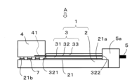
- FIG. 1 is a plan view showing a mounting structure in which optical components and electronic components are mounted on an optical circuit board according to an embodiment of the present disclosure.
- 2 is an enlarged explanatory view for illustrating a cross section of a region X shown in FIG. 1 .
- FIG. 3A is a plan view of a main part of the optical waveguide as viewed from the direction of the arrow A shown in FIG. 2
- B is an enlarged explanatory view (perspective view) for explaining the region Y shown in FIG. 3A
- C is a front view of the optical waveguide as viewed from the direction of the arrow B shown in FIG. 3A.
- 1A to 1C are explanatory diagrams for explaining an embodiment of a method for forming an optical waveguide in a wiring board.
- FIG. 5A is a plan view showing another embodiment of the main part of the optical waveguide as viewed from the direction of the arrow A shown in FIG. 2
- FIG. 5B is an enlarged explanatory view showing a cross section taken along the line X-X shown in FIG. 5A
- FIG. 5C is a side view of the optical circuit board (optical waveguide) as viewed from the direction of the arrow C shown in FIG. 5B
- 6A is an explanatory diagram (oblique view) for explaining yet another embodiment of the recesses (first recess and second recess) formed in the optical waveguide
- FIG. 6B is a plan view seen from the direction of arrow D shown in FIG. 6A
- FIG. 13A is an explanatory view (perspective view) for explaining still another embodiment of the recesses (first recess and second recess) formed in the optical waveguide.
- the array illumination optical system which is the light source
- the array illumination optical system may mistakenly recognize the side end of the upper cladding of the optical waveguide as the core portion.
- manual readjustment is required, which reduces the efficiency of the inspection. Therefore, there is a demand for an optical circuit board that allows for efficient inspection of optical waveguides.
- Figure 1 is a plan view showing a mounting structure 10 in which an optical component 4 and an electronic component 6 are mounted on an optical circuit board 1 according to one embodiment of the present disclosure.
- Such a wiring board 2 includes, for example, a core layer and build-up layers laminated on both sides of the core layer, although not specifically illustrated.
- the core layer includes a core insulating layer and a core conductor layer.
- the core insulating layer is not particularly limited as long as it is made of an insulating material. Examples of insulating materials include resins such as epoxy resin, bismaleimide-triazine resin, polyimide resin, and polyphenylene ether resin. Only one type of these resins may be used, or two or more types may be used in combination.
- the core insulating layer may contain a reinforcing material.
- reinforcing materials include insulating cloth materials such as glass fiber, glass nonwoven fabric, aramid nonwoven fabric, aramid fiber, and polyester fiber. Only one type of reinforcing material may be used, or two or more types may be used in combination.
- the core insulating layer may have inorganic insulating fillers such as silica, barium sulfate, talc, clay, glass, calcium carbonate, and titanium oxide dispersed therein. Only one type of inorganic insulating filler may be used, or two or more types may be used in combination.
- the core conductor layer is located on the surface of the core insulating layer.
- the core conductor layer is not particularly limited as long as it is made of a material that is conductive. Examples of conductive materials include metals such as copper.
- a through-hole conductor is located to electrically connect the upper and lower surfaces of the core insulating layer.
- the through-hole conductor is located in a through-hole that penetrates the upper and lower surfaces of the core insulating layer.
- the through-hole conductor is formed of a metal such as copper.
- the through-hole conductor may be formed only on the inner wall surface, or may be filled in the through-hole.
- the through-hole conductor is connected to the core conductor layer on the surface of the core insulating layer.
- the build-up layer is located on one or both sides of the core layer.
- the build-up layer has a structure in which at least one build-up insulating layer and at least one build-up conductor layer are laminated.
- the build-up insulating layer is not particularly limited as long as it is made of an insulating material. Examples of insulating materials include resins such as epoxy resins, bismaleimide-triazine resins, polyimide resins, and polyphenylene ether resins. These resins may be used alone or in combination of two or more types.
- the build-up insulation layers may be made of the same resin or different resins.
- the build-up insulation layers and the core insulation layers may be made of the same resin or different resins.
- the build-up layers usually have via-hole conductors to electrically connect the layers.
- the build-up insulating layer may contain a reinforcing material.
- reinforcing materials include insulating cloth materials such as glass fiber, glass nonwoven fabric, aramid nonwoven fabric, aramid fiber, and polyester fiber. Only one type of reinforcing material may be used, or two or more types may be used in combination.
- the build-up insulating layer may have inorganic insulating fillers such as silica, barium sulfate, talc, clay, glass, calcium carbonate, and titanium oxide dispersed therein. Only one type of inorganic insulating filler may be used, or two or more types may be used in combination.
- the conductor layer for the build-up is not particularly limited as long as it is made of a material that is conductive, similar to the conductor layer for the core.
- a material that is conductive is a metal such as copper.
- the optical waveguide 3 included in the optical circuit board 1 is located on the surface of the metal layer 21a present on the surface of the wiring board 2.
- FIG. 2 is an enlarged explanatory diagram for explaining the cross section of region X shown in FIG. 1.
- the optical waveguide 3 has a structure in which a lower clad 31, a core 32, and an upper clad 33 are layered in this order from the metal layer 21a side.
- the lower cladding 31 included in the optical waveguide 3 is located on the first surface 21 of the wiring board 2, specifically on the surface of the metal layer 21a present on the surface of the optical waveguide forming region of the wiring board 2.
- the material forming the lower cladding 31 is not limited, and examples include resins such as epoxy resin and silicone resin.
- the lower cladding 31 has a second surface 312 located on the opposite side to the surface facing the first surface 21 of the wiring board 2.
- the metal layer 21a is an optional member and may or may not be used. In other words, the wiring board 2 does not need to include the metal layer 21a.
- the upper clad 33 included in the optical waveguide 3 is positioned so as to cover the upper surface of the lower clad 31 and the core 32.
- the upper clad 33 is also formed of a resin such as epoxy resin or silicone resin.
- the lower clad 31 and the upper clad 33 may be made of the same material or different materials.
- the lower clad 31 and the upper clad 33 may have the same thickness or different thicknesses.
- the lower clad 31 and the upper clad 33 each have a thickness of, for example, 5 ⁇ m or more and 150 ⁇ m or less.
- the core 32 included in the optical waveguide 3 is a portion through which light that has entered the optical waveguide 3 propagates.
- the core 32 extends to the second surface 312 of the lower cladding 31, and has a first end surface 321 and a second end surface 322 that are positioned opposite each other in the extending direction of the core 32.
- the first end surface 321 of the core 32 is the end surface on the optical component 4 side
- the second end surface 322 of the core 32 is the end surface on the optical connector 5a side.
- the end face of the optical transmission path (Si waveguide) 41 included in the optical component 4 mounted in the mounting area of the wiring board 2 is positioned to face the first end face 321 of the core 32 of the optical waveguide 3.
- optical signals are transmitted and received between the core 32 and the optical transmission path 41.
- the material forming the core 32 is not limited, and is appropriately set taking into consideration, for example, the light transmittance and the wavelength characteristics of the propagating light. Examples of materials include resins such as epoxy resin and silicone resin.
- the core 32 has a thickness of, for example, 3 ⁇ m or more and 50 ⁇ m or less.
- the upper clad 33 has a first side surface 331 and a second side surface 332 located along the extension direction of the core 32, a third surface 333 located on the opposite side of the surface that contacts the second surface 312 of the lower clad 31, a first side portion 33a which is a tangent portion between the first side surface 331 and the third surface 333, and a second side portion 33b which is a tangent portion between the second side surface 332 and the third surface 333.
- Figure 3A is a plan view of the main part of the optical waveguide 3 as seen from the direction of the arrow A shown in Figure 2.
- Figure 3B is an enlarged explanatory view (perspective view) for explaining the region Y shown in Figure 3A.
- FIG. 3C is a front view of the optical waveguide 3 as seen from the direction of arrow B shown in FIG. 3A.
- At least one recess 33c is located in the upper cladding 33.
- at least one of a first recess 33c1 that contacts the first side portion 33a and opens to the third surface 333 and the first side surface 331, and a second recess 33c2 that contacts the second side portion 33b and opens to the third surface 333 and the second side surface 332 is located in the upper cladding 33.
- the first recess 33c1 and the second recess 33c2 are described separately only for convenience, and the first recess 33c1 and the second recess 33c2 may be collectively referred to as recess 33c.
- the optical circuit board 1 has at least one such recess 33c on at least one of the first side 33a and the second side 33b of the upper clad 33, which allows efficient optical waveguide inspection. Specifically, when inspecting the transmission and reception of optical signals by irradiating light to the core 32 of the optical waveguide 3 before mounting the optical components 4 on the optical circuit board 1 according to one embodiment, the presence of the recess 33c causes the light trapped by the refractive index difference between the upper clad 33 and the air to be scattered by the recess 33c.
- At least one recess 33c is located in the upper cladding 33, and multiple recesses 33c may be located.
- multiple recesses 33c may be located.
- at least one of the first recesses 33c1 and the second recesses 33c2 may be located multiple times, or multiple of each may be located.
- the irradiated light is scattered more, and the transmission of light to the edge portion of the upper cladding 33 is more efficiently reduced.
- the recesses 33c (first recess 33c1 and second recess 33c2) have a rectangular shape when viewed from above in a plan view.
- the size of the recesses 33c is not limited and is set appropriately depending on the size of the optical waveguide 3, etc., so as to scatter the irradiated light.
- the width W may be, for example, 5 ⁇ m or more and 20 ⁇ m or less.
- the length L may be, for example, 5 ⁇ m or more and 500 ⁇ m or less.
- the length L is 10 ⁇ m or more and 50 ⁇ m or less, the irradiated light is more scattered, and the transmission of light to the edge of the upper cladding 33 is more efficiently reduced. If the width W is 10 ⁇ m or more and 50 ⁇ m or less, the range in which light is trapped due to the difference in refractive index between the upper cladding 33 and air can be covered.
- the height H of the recess 33c corresponds to the thickness of the upper clad 33.
- the height H of the recess 33c may be less than the thickness of the upper clad 33. That is, in the recess 33c, the bottom farthest from the third surface 333 of the upper clad 33 may be located on the second surface 312 of the upper clad 33 or the lower clad 31. In FIG. 3B, this bottom is located on the second surface 312 of the lower clad 31.
- the arithmetic mean roughness of the inner wall surface of the recess 33c is not limited. In at least a portion of the recess 33c, the arithmetic mean roughness of the inner wall surface may be, for example, 50 nm or less. When the arithmetic mean roughness is 50 nm or less, the surface is mirror-like, and the irradiated light can be efficiently reflected in a direction different from the irradiation direction. As a result, the light transmission through the first side portion 33a and the second side portion 33b is more efficiently reduced.
- the arithmetic mean roughness can be calculated by measuring any inner wall surface of the recess 33c using a laser displacement meter, optical interference measuring device, or the like, for example, after the recess 33c is formed.
- the method for forming the recess 33c in the edge portion of the upper cladding 33 is not limited, and for example, the recess 33c is formed by the following procedure.
- One embodiment of the method for forming the recess 33c will be described with reference to FIG. 4.
- FIG. 4 is an explanatory diagram for explaining one embodiment of the method for forming the optical waveguide 3 in the wiring board 2.
- the wiring board 2 is omitted from FIG. 4B.
- a lower clad 31 is formed on the first surface 21 of the wiring board 2.
- a metal layer 21a may be located between the lower clad 31 and the first surface 21.
- upper clad material 33d which will be the material of upper clad 33, is attached to second surface 312 of lower clad 31 so that first end surface 321 and second end surface 322 of core 32 are exposed.
- the material forming upper clad 33 is as described above, and detailed description will be omitted.
- the surface of upper clad material 33d is covered with mask 35.
- the portion covered with mask 35 is the portion that will be removed by development after exposure. Specifically, when viewed in a plan view from above, both sides of upper clad material 33d and the portion that will form recess 33c should be covered with mask 35 so as to follow core 32.
- the upper cladding material 33d is hardened by exposure to light. Then, as shown in FIG. 4E, the mask 35 is removed, and the upper cladding material 33d in the portion covered by the mask 35 is removed by development. Through this procedure, as shown in FIG. 4E, a first recess 33c1 that contacts the first side portion 33a and opens to the third surface 333 and the first side surface 331, and a second recess 33c2 that contacts the second side portion 33b and opens to the third surface 333 and the second side surface 332 are formed in the upper cladding 33.
- FIG. 4E illustrates an example in which there is one each of the first recess 33c1 and the second recess 33c2, the number of recesses 33c can be adjusted according to the shape of the mask 35.
- Figure 5A is a plan view showing another embodiment of the main part of the optical waveguide 3 as viewed from the direction of the arrow A shown in Figure 2.
- Figure 5B is an enlarged explanatory view showing a cross section taken along line X-X shown in Figure 5A.
- Figure 5C is a side view of the optical circuit board 1 (optical waveguide 3) as viewed from the direction of the arrow C shown in Figure 5B.
- the bottom farthest from the third surface 333 of the upper clad 33 is located on the second surface 312 of the lower clad 31. That is, the height H of the recess 33c (33c2) corresponds to the thickness of the upper clad 33.
- the height of the recess 33c shown in FIG. 5B is greater than the thickness of the upper clad 33. In this way, in the recess 33c, the bottom farthest from the third surface 333 of the upper clad 33 may be located closer to the first surface 21 of the wiring board 2 than the second surface 312 of the lower clad 31. When multiple recesses 33c are located, it is sufficient that at least some of the recesses 33c have such a structure.
- the sealing resin 8 that connects the optical component 4 and the optical connector 5a enters the recess 33c.
- the bonding strength between these components is improved.
- the bottom is flat in FIG. 5B, it may be uneven. In this case, the contact area between the sealing resin 8 and the bottom is increased, which is advantageous in that the bonding strength is improved.
- the bottom of the recess 33c which is furthest from the third surface 333 of the upper cladding 33, is not limited as long as it is located closer to the first surface 21 than the second surface 312 of the lower cladding 31.
- the bottom may be located at a depth from the second surface 312 to 100% or more of the thickness of the lower cladding 31. In other words, the recess 33c may penetrate the lower cladding 31.
- the recess 33c whose bottom is located closer to the first surface 21 than the second surface 312 of the lower clad 31, is formed, for example, by laser processing.
- the mask 35 shown in FIG. 4D is not used to form the recess 33c, but is used so that only the first side surface 331 and the second side surface 332 of the upper clad 33 are formed.
- the upper clad material 33d in the portion not covered by the mask 35 is hardened.
- the upper clad material 33d in the portion covered by the mask 35 is removed by development.
- the recess 33c is then formed by subjecting it to laser processing.
- Fig. 6A is an explanatory diagram (perspective view) for explaining yet another embodiment of the recess 33c (first recess 33c1 and second recess 33c2) formed in the optical waveguide 3.
- Fig. 6B is a plan view seen from the direction of the arrow D shown in Fig. 6A.
- the convex portion 334 When the convex portion 334 is located in the concave portion 33c, for example, a portion of the light incident from the first end face 321 side and entering the concave portion 33c is reflected at the convex portion 334 to the outside of the optical waveguide 3, making it easier to reduce the light transmitted to the second end face 322 side.
- the angle ⁇ between the incident direction F of the light and the convex portion 334 is not limited, and may be, for example, 15° or more and 75° or less. If the angle ⁇ is in this range, it becomes easier to reflect the light incident on the first side portion 33a and the second side portion 33b of the upper cladding 33 to the outside of the optical waveguide 3. When multiple concave portions 33c are located, it is sufficient that at least some of the concave portions 33c have convex portions 334.
- the convex portion 334 when viewed from above in a plane, has a triangular shape. However, if the angle ⁇ is less than 90°, the shape of the convex portion 334 is not limited to a triangular shape. When viewed in a plane, the convex portion 334 may have, for example, a semicircular shape or a trapezoidal shape.
- the recess 33c shown in Figures 3 to 5 has a rectangular shape when viewed from above in a plan view.
- the third surface 333 and the side surface of the upper cladding 33 have a rectangular cutout shape so as to have an opening.
- the shape of the recess 33c is not limited to a rectangular shape.
- the shape of the recess 33c is not limited as long as it is in contact with the first side 33a (second side 33b) of the upper cladding 33 and opens to the third surface 333 and the first side surface 331 (second side surface 332) of the upper cladding 33.
- Figure 7 is an explanatory diagram (perspective view) for explaining yet another embodiment of the recess 33c (first recess 33c1 and second recess 33c2) formed in the optical waveguide 3.
- the third surface 333 and the side surface of the upper cladding 33 may have a triangular cutout shape so as to have an opening, or may have a semicircular, trapezoidal, or other cutout shape.
- a mounting structure 10 has a structure in which an optical component 4 and an electronic component 6 are mounted on an optical circuit board 1 according to an embodiment.
- the optical component 4 mounted on the mounting structure 10 according to an embodiment includes an optical transmission path 41.
- optical components 4 including such optical transmission paths 41 include silicon photonics devices.
- electronic components 6 include ASICs (Application Specific Integrated Circuits) and driver ICs.
- the optical component 4 is electrically connected to the wiring board 2. Specifically, the optical component 4 is electrically connected to a pad 21b located in the mounting area (area for mounting the optical component 4) of the wiring board 2 via solder 7.
- the pad 21b is part of a conductor layer located on the upper surface of the wiring board 2.
- a silicon photonics device will be described as an example of the optical component 4.
- the silicon photonics device is, for example, a type of optical component having an optical transmission path 41 with a core of silicon (Si) and a clad of silicon dioxide (SiO 2 ).
- the silicon photonics device includes a Si waveguide as the optical transmission path 41, and further includes a passivation film, a light source unit, a light detection unit, and the like, although not shown.
- the optical transmission path 41 (Si waveguide 41) is located at one end of the optical waveguide 3 (first end surface 321 in FIG. 2) so as to face the core 32 included in the optical waveguide 3.
- an electrical signal from the wiring board 2 is transmitted via the solder 7 to the light source section included in the optical component 4 (silicon photonics device).
- the light source section receives the transmitted electrical signal and emits light.
- the emitted optical signal is transmitted via the optical transmission path 41 (Si waveguide 41) and the core 32 to the optical fiber 5 connected via the optical connector 5a.
- the optical circuit board includes a wiring board having a first surface and an optical waveguide located on the first surface.
- the optical waveguide includes a lower cladding, a core, and an upper cladding.
- the lower cladding is located on the first surface and has a second surface located opposite the surface in contact with the first surface.
- the core extends on the second surface and has a first end surface and a second end surface located opposite each other in the extension direction of the core.
- the upper cladding is located on the second surface and covers the core so that the first end surface and the second end surface are exposed, and has a pair of first and second side surfaces located along the extension direction, a third surface located opposite the surface in contact with the second surface, a first edge portion that is a tangent portion between the first side surface and the third surface, and a second edge portion that is a tangent portion between the second side surface and the third surface.
- the upper cladding further has at least one of a first recess that contacts the first edge portion and opens to the third surface and the first side surface, and a second recess that contacts the second edge portion and opens to the third surface and the second side surface.
- the upper clad has at least one of the first recesses and the second recesses in a plurality of portions.
- the upper clad has a plurality of first recesses and a plurality of second recesses.
- the bottom portion farthest from the third surface is located on the upper cladding or the second surface.
- the bottom furthest from the third surface is located closer to the first surface than the second surface in the lower cladding.
- the mounting structure according to the present disclosure includes an optical circuit board described in any one of (1) to (7) above, and an optical component mounted on the optical circuit board.
Landscapes
- Physics & Mathematics (AREA)
- Engineering & Computer Science (AREA)
- Microelectronics & Electronic Packaging (AREA)
- General Physics & Mathematics (AREA)
- Optics & Photonics (AREA)
- Optical Integrated Circuits (AREA)
- Optical Couplings Of Light Guides (AREA)
Priority Applications (1)
| Application Number | Priority Date | Filing Date | Title |
|---|---|---|---|
| JP2025510882A JPWO2024204111A1 (https=) | 2023-03-30 | 2024-03-25 |
Applications Claiming Priority (2)
| Application Number | Priority Date | Filing Date | Title |
|---|---|---|---|
| JP2023055554 | 2023-03-30 | ||
| JP2023-055554 | 2023-03-30 |
Publications (1)
| Publication Number | Publication Date |
|---|---|
| WO2024204111A1 true WO2024204111A1 (ja) | 2024-10-03 |
Family
ID=92906631
Family Applications (1)
| Application Number | Title | Priority Date | Filing Date |
|---|---|---|---|
| PCT/JP2024/011777 Ceased WO2024204111A1 (ja) | 2023-03-30 | 2024-03-25 | 光回路基板および実装構造体 |
Country Status (2)
| Country | Link |
|---|---|
| JP (1) | JPWO2024204111A1 (https=) |
| WO (1) | WO2024204111A1 (https=) |
Citations (4)
| Publication number | Priority date | Publication date | Assignee | Title |
|---|---|---|---|---|
| JP2005266254A (ja) * | 2004-03-18 | 2005-09-29 | Sanyo Electric Co Ltd | 光導波路 |
| US20090304324A1 (en) * | 2008-06-09 | 2009-12-10 | Samsung Electro-Mechanics Co., Ltd. | Optical waveguide and optical printed circuit board having the same |
| JP2014211510A (ja) * | 2013-04-18 | 2014-11-13 | 日東電工株式会社 | 光電気混載モジュール |
| JP2015087657A (ja) * | 2013-10-31 | 2015-05-07 | 住友ベークライト株式会社 | 光導波路、光電気混載基板および電子機器 |
-
2024
- 2024-03-25 WO PCT/JP2024/011777 patent/WO2024204111A1/ja not_active Ceased
- 2024-03-25 JP JP2025510882A patent/JPWO2024204111A1/ja active Pending
Patent Citations (4)
| Publication number | Priority date | Publication date | Assignee | Title |
|---|---|---|---|---|
| JP2005266254A (ja) * | 2004-03-18 | 2005-09-29 | Sanyo Electric Co Ltd | 光導波路 |
| US20090304324A1 (en) * | 2008-06-09 | 2009-12-10 | Samsung Electro-Mechanics Co., Ltd. | Optical waveguide and optical printed circuit board having the same |
| JP2014211510A (ja) * | 2013-04-18 | 2014-11-13 | 日東電工株式会社 | 光電気混載モジュール |
| JP2015087657A (ja) * | 2013-10-31 | 2015-05-07 | 住友ベークライト株式会社 | 光導波路、光電気混載基板および電子機器 |
Also Published As
| Publication number | Publication date |
|---|---|
| JPWO2024204111A1 (https=) | 2024-10-03 |
| TW202501063A (zh) | 2025-01-01 |
Similar Documents
| Publication | Publication Date | Title |
|---|---|---|
| JP7617248B2 (ja) | 光回路基板およびそれを用いた光学部品実装構造体 | |
| CN114127601B (zh) | 光电路基板以及使用了该光电路基板的电子部件安装构造体 | |
| JP7515609B2 (ja) | 光回路基板およびそれを用いた電子部品実装構造体 | |
| TWI693437B (zh) | 光波導及光電路基板 | |
| WO2023162964A1 (ja) | 光回路基板 | |
| WO2024204111A1 (ja) | 光回路基板および実装構造体 | |
| TWI866040B (zh) | 光迴路基板及光學零件構裝構造體 | |
| TWI917915B (zh) | 光迴路基板及安裝構造體 | |
| US12481109B2 (en) | Optical circuit board and electronic component mounting structure using the same | |
| JP7710784B2 (ja) | 光回路基板および光学部品実装構造体 | |
| US20250216606A1 (en) | Optical circuit board | |
| JP7788203B2 (ja) | 光回路基板およびそれを用いた光学部品実装構造体 | |
| WO2025206001A1 (ja) | 光回路基板および実装構造体 | |
| WO2025182787A1 (ja) | 光回路基板および実装構造体 | |
| WO2024143134A1 (ja) | 光回路基板、光学部品実装構造体および光回路基板の製造方法 | |
| WO2025183093A1 (ja) | 光回路基板および実装構造体 | |
| WO2025205531A1 (ja) | 光回路基板および実装構造体 | |
| WO2024117023A1 (ja) | 光回路基板、光学部品実装構造体および光回路基板の製造方法 |
Legal Events
| Date | Code | Title | Description |
|---|---|---|---|
| 121 | Ep: the epo has been informed by wipo that ep was designated in this application |
Ref document number: 24780227 Country of ref document: EP Kind code of ref document: A1 |
|
| ENP | Entry into the national phase |
Ref document number: 2025510882 Country of ref document: JP Kind code of ref document: A |
|
| WWE | Wipo information: entry into national phase |
Ref document number: 2025510882 Country of ref document: JP |
|
| NENP | Non-entry into the national phase |
Ref country code: DE |
|
| 122 | Ep: pct application non-entry in european phase |
Ref document number: 24780227 Country of ref document: EP Kind code of ref document: A1 |