WO2024203461A1 - 液晶材料を用いたリフレクトアレイ - Google Patents
液晶材料を用いたリフレクトアレイ Download PDFInfo
- Publication number
- WO2024203461A1 WO2024203461A1 PCT/JP2024/010265 JP2024010265W WO2024203461A1 WO 2024203461 A1 WO2024203461 A1 WO 2024203461A1 JP 2024010265 W JP2024010265 W JP 2024010265W WO 2024203461 A1 WO2024203461 A1 WO 2024203461A1
- Authority
- WO
- WIPO (PCT)
- Prior art keywords
- bias
- wiring
- liquid crystal
- electrodes
- common electrodes
- Prior art date
- Legal status (The legal status is an assumption and is not a legal conclusion. Google has not performed a legal analysis and makes no representation as to the accuracy of the status listed.)
- Ceased
Links
Images


Classifications
-
- H—ELECTRICITY
- H01—ELECTRIC ELEMENTS
- H01Q—ANTENNAS, i.e. RADIO AERIALS
- H01Q15/00—Devices for reflection, refraction, diffraction or polarisation of waves radiated from an antenna, e.g. quasi-optical devices
- H01Q15/14—Reflecting surfaces; Equivalent structures
- H01Q15/147—Reflecting surfaces; Equivalent structures provided with means for controlling or monitoring the shape of the reflecting surface
-
- H—ELECTRICITY
- H01—ELECTRIC ELEMENTS
- H01Q—ANTENNAS, i.e. RADIO AERIALS
- H01Q15/00—Devices for reflection, refraction, diffraction or polarisation of waves radiated from an antenna, e.g. quasi-optical devices
- H01Q15/14—Reflecting surfaces; Equivalent structures
- H01Q15/148—Reflecting surfaces; Equivalent structures with means for varying the reflecting properties
-
- H—ELECTRICITY
- H01—ELECTRIC ELEMENTS
- H01Q—ANTENNAS, i.e. RADIO AERIALS
- H01Q3/00—Arrangements for changing or varying the orientation or the shape of the directional pattern of the waves radiated from an antenna or antenna system
- H01Q3/44—Arrangements for changing or varying the orientation or the shape of the directional pattern of the waves radiated from an antenna or antenna system varying the electric or magnetic characteristics of reflecting, refracting, or diffracting devices associated with the radiating element
Definitions
- One embodiment of the present invention relates to a radio wave reflector (hereinafter also referred to as a "reflectarray”) that can change the direction of reflection of radio waves, and in particular to a reflectarray that uses a liquid crystal material.
- a radio wave reflector hereinafter also referred to as a "reflectarray”
- a reflectarray that uses a liquid crystal material.
- Reflectarrays are used to deliver radio waves to areas where radio waves have difficulty reaching (dead zones), such as the gaps between high-rise buildings.
- Examples of reflectarrays disclosed include a configuration in which a main array element (dipole element), a subarray element (parasitic element), and a common electrode (ground electrode) are arranged on either side of a dielectric substrate, with the subarray element disposed adjacent to the main array element (Patent Document 1), and a configuration in which the array element and the common electrode (ground electrode) sandwich a dielectric substrate, with the common electrode having a periodic loop shape (Patent Document 2).
- Reflectarrays use a dielectric substrate, but if the part equivalent to this dielectric substrate is replaced with a liquid crystal layer, the dielectric anisotropy of the liquid crystal material can be utilized, making it possible to vary the directionality of the reflected waves.
- Reflectarrays using liquid crystal materials have a structure similar to that of planar array antennas in which a patch array is arranged.
- radio waves reflected by a reflectarray In addition to the main lobe that is reflected at the desired angle, radio waves reflected by a reflectarray also have side lobes that are reflected diagonally and horizontally to that angle. Since side lobes are not radio waves that are reflected in the desired direction, if the side lobes are large, the reflection gain decreases and they become a source of noise that reduces the communication quality on the receiving side.
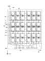
- FIG. 1 is a plan view showing a configuration of a reflect array according to an embodiment of the present invention.
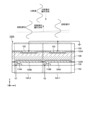
- 2 is a diagram showing a cross-sectional structure of a reflect array corresponding to the area A1-A2 shown in FIG.
- FIG. 2 is a plan view showing a unit cell that constitutes a reflective element according to one embodiment of the present invention.
- FIG. 4 is a diagram showing a cross-sectional structure of a unit cell taken along line B1-B2 shown in FIG.
- FIG. 13 is a diagram for explaining the operation of a unit cell constituting a reflective element according to one embodiment of the present invention, showing a state in which no bias voltage is applied to a liquid crystal layer.
- FIG. 1 is a plan view showing a configuration of a reflect array according to an embodiment of the present invention.
- 2 is a diagram showing a cross-sectional structure of a reflect array corresponding to the area A1-A2 shown in FIG.
- FIG. 2 is a plan view showing a unit cell that
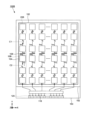
- FIG. 1 is a diagram showing a configuration of a common electrode constituting a unit cell according to an embodiment of the present invention, and strip wiring connecting the common electrodes to each other;
- 1 is a diagram showing a configuration of a common electrode constituting a unit cell according to an embodiment of the present invention, and strip wiring connecting the common electrodes to each other;
- 10 is a diagram illustrating that the amplitude of a reflected wave can be fitted to a Taylor distribution by changing the length of the strip wiring.
- FIG. 1 shows the results of calculating the array factor of a one-dimensional unit cell array in one embodiment of the present invention.
- FIG. 1 is a plan view showing a configuration of a reflect array according to an embodiment of the present invention.
- 11 is a diagram showing a cross-sectional structure of a reflect array corresponding to the area between C1 and C2 shown in FIG. 10.
- FIG. 11 is a diagram for explaining an array factor obtained in the first embodiment.
- the reflect array using the liquid crystal material according to this embodiment has a structure in which a common electrode is provided on the radio wave incident surface side, and a bias electrode is provided on the rear side of the common electrode with a liquid crystal layer used as a dielectric layer sandwiched therebetween. Details thereof will be described below with reference to the drawings.
- Reflectarray Fig. 1 shows a plan view of the reflectarray 100A according to this embodiment.
- Fig. 2 shows a cross-sectional structure of the reflectarray 100A corresponding to the A1-A2 area shown in Fig. 1.
- the reflectarray 100A includes a common electrode 102, a bias electrode 104, and a liquid crystal layer 106 disposed between the common electrode 102 and the bias electrode 104.
- the common electrodes 102 are arranged in a matrix in the X-axis and Y-axis directions.
- the bias electrodes 104 are arranged in a matrix in the X-axis and Y-axis directions to correspond to the common electrodes 102.
- the common electrodes 102 and the bias electrodes 104 are arranged so as to overlap in a planar view.
- the X-axis and Y-axis directions are used for explanation purposes and refer to the directions shown in FIG. 1.
- the X-axis and Y-axis directions can also be interpreted as a first direction and a second direction intersecting the first direction.
- the common electrode 102 has a planar shape similar to that of a patch antenna, and is arranged at a distance from each unit cell 10A.
- the bias electrode 104 is arranged corresponding to the common electrode 102.
- the reflect array 100A can also be said to have a structure in which such unit cells 10A are arranged in a matrix in the X-axis direction and the Y-axis direction. There is no limit to the number of unit cells 10A arranged in the X-axis direction and the Y-axis direction, but 10 or more, preferably 16 or more are arranged in the Y-axis direction.
- the common electrodes 102 are connected to adjacent common electrodes 102 in the Y-axis direction by strip wiring 108.
- FIG. 1 shows a structure in which the common electrodes 102 arranged in the Y-axis direction are connected to each other by strip wiring 108.
- the bias electrodes 104 are arranged in a state where they are physically and electrically separated from adjacent bias electrodes 104. Therefore, the unit cells 10A arranged in the Y-axis direction have a structure in which a common common voltage is applied to the common electrodes 102, and bias signals can be applied to the bias electrodes 104 individually. In this embodiment, for ease of explanation, such an arrangement of unit cells 10A in the Y-axis direction is referred to as a unit cell array 20A.
- the reflect array 100A includes a selection signal line 112 extending in the X-axis direction, a bias signal line 114 extending in the Y-axis direction, and a switching element 110.
- the selection signal line 112, the bias signal line 114, and the switching element 110 are provided on the second substrate 152.
- the selection signal line 112 extends in the X-axis direction
- the bias signal line 114 extends in the Y-axis direction.
- the switching element 110 is provided for each unit cell 10A.
- the on and off states of the switching element 110 are controlled by a selection signal from the selection signal line 112. When the switching element 110 is in the on state, a bias voltage based on a bias signal is applied from the bias signal line 114 to the bias electrode 104.
- the selection signal line 112 and the bias signal line 114 are arranged to cross each other, but the two lines are insulated by providing an interlayer insulating layer 130 on the second substrate 152.
- the second substrate 152 may also be provided with a selection signal line drive circuit 116 that outputs a selection signal to the selection signal line 112, a bias signal line drive circuit 118 that outputs a bias signal to the bias signal line 114, and a terminal section 120 for inputting a control signal from an external circuit.
- the liquid crystal layer 106 contains rod-shaped, elongated liquid crystal molecules. Because the liquid crystal molecules have dielectric anisotropy, the dielectric constant changes as the orientation state of the liquid crystal molecules changes.
- the phase of the radio waves reflected by the reflect array 100A changes depending on the dielectric constant of the liquid crystal layer 106. By changing the dielectric constant of the liquid crystal layer 106 for each unit cell 10A within the plane of the reflect array 100A, a phase difference is generated in the reflected radio waves, making it possible to control the traveling direction (reflection direction) to the intended direction.
- the initial alignment state of the liquid crystal molecules in the liquid crystal layer 106 is determined by the alignment film.
- a first alignment film 122A is provided on the first substrate 150, and a second alignment film 122B is provided on the second substrate 152.
- the first alignment film 122A is provided so as to cover the common electrode 102, and the second alignment film 122B is provided so as to cover the bias electrode 104.
- the first alignment film 122A and the second alignment film 122B only need to have the function of orienting the liquid crystal molecules, and there are no limitations on the material and manufacturing method.
- the first alignment film 122A and the second alignment film 122B are appropriately selected from vertical alignment films, horizontal alignment films, etc. according to the type of liquid crystal.
- the first alignment film 122A and the second alignment film 122B are formed of, for example, polyimide.
- the reflect array 100A has a structure similar to that of a liquid crystal display panel in which a liquid crystal layer 106 is provided between a pair of opposing electrodes (common electrode 102 and bias electrode 104), but differs in that the liquid crystal layer 106 is thick and the common electrode 102 and bias electrode 104 are not transparent, as described below. Rather, the reflect array 100A can be considered as a patch antenna in which a patch electrode (common electrode 102) is provided on the upper surface of the dielectric (liquid crystal layer 106) and a reflective electrode (bias electrode) is provided on the back surface.
- a patch electrode common electrode 102
- a reflective electrode bias electrode
- FIG. 3 and 4 show details of the unit cell 10A constituting the reflect array 100A.
- Fig. 3 shows a plan view of the unit cell 10A
- Fig. 4 shows a cross-sectional structure of the unit cell 10A corresponding to the section B1-B2 shown in Fig. 3.
- the unit cell 10A has a structure in which the common electrode 102, the liquid crystal layer 106, and the bias electrode 104 overlap in a planar view.
- Figure 3 shows an example in which the shape of the common electrode 102 in a planar view is square.
- the shape of the common electrode 102 is not limited to the shape shown in Figure 3, and it may be rectangular, or may have a geometric shape such as a rectangle with the corners cut out.
- the size (length and width) of the common electrode 102 is set appropriately according to the frequency of the target radio wave.
- the length and width of the common electrode 102 can be set so that it has a shape that is symmetrical with respect to the vertical polarization and horizontal polarization of the incident radio wave.
- the common electrode 102 is connected to the strip wiring 108.
- the strip wiring 108 is connected to the center of one side of the common electrode 102.
- the strip wiring 108 is connected so that the center point of one side of the common electrode 102 is included in the width portion of the strip wiring 108.
- the connection structure between the strip wiring 108 and the common electrode 102 may be formed from the same conductive layer, or the strip wiring 108 and the common electrode 102 may be provided with an interlayer insulating layer between them and connected via a contact hole.
- the strip wiring 108 is a wiring that connects the common electrodes 102 arranged in the Y-axis direction. As described later, the spacing between the common electrodes 102 arranged in the Y-axis direction is constant, whereas the wiring length of the strip wiring 108 varies depending on the position of the unit cell 10A arranged in the Y-axis direction.
- FIG. 1 shows two unit cells 10A, one arranged in the center of the unit cell array 20A and one arranged at the end (outside), and the length of the strip wiring 108 is long in the center of the unit cell array 20A, and gradually changes (becomes gradually shorter) from the center to the outside.
- the bias electrode 104 has a larger area than the common electrode 102 in order to function as a reflector.
- the bias electrode 104 and the common electrode 102 are arranged so as to overlap, with the common electrode 102 being arranged so as to be contained within the bias electrode 104.
- the bias electrode 104 is connected to the bias signal line 114 via the switching element 110.
- the switching element 110 is formed of a transistor.
- the transistor has a structure in which a semiconductor layer 124, a gate insulating layer 126, and a gate electrode 128 are stacked.
- An interlayer insulating layer 130 is provided on the gate electrode 128, and a bias signal line 114 is provided on the interlayer insulating layer 130.
- the switching element 110 and the bias signal line 114 are embedded in a planarization layer 132.
- the bias electrode 104 is provided on a flat surface on the planarization layer 132.
- the bias electrode 104 is connected to the input/output terminal (drain) of the switching element 110 (transistor) through a contact hole.
- the gate electrode 128 of the switching element 110 (transistor) is connected to the selection signal line 112, and the input/output terminal (source) that is not connected to the bias electrode 104 is connected to the bias signal line 114.
- the bias signal is a DC voltage signal or a polarity-reversed DC voltage signal in which a positive DC voltage and a negative DC voltage are alternately reversed.
- the liquid crystal layer 106 is formed of a liquid crystal material that exhibits liquid crystallinity and has dielectric anisotropy.
- the liquid crystal material may have either positive or negative dielectric anisotropy.
- the liquid crystal layer 106 is formed of, for example, nematic liquid crystal.
- the frequency bands of radio waves reflected by the reflect array 100A are the very high frequency (VHF) band, the ultra-high frequency (UHF) band, the super high frequency (SHF) band, the submillimeter wave (THF) band, the extra high frequency (EHF) band, and the terahertz wave band.
- VHF very high frequency
- UHF ultra-high frequency
- SHF super high frequency
- THF submillimeter wave
- EHF extra high frequency
- terahertz wave band the terahertz wave band.
- the orientation state of the liquid crystal molecules in the liquid crystal layer 106 changes depending on the bias signal (bias voltage) applied to the bias electrode 104, but does not follow the frequency of the radio waves incident on the common electrode 102 at all.
- the reflect array 100A Since the orientation of the liquid crystal molecules does not change in response to high frequencies, the reflect array 100A has the function of changing the dielectric constant of the liquid crystal layer 106 by the bias electrode 104, and at the same time reflecting the radio waves at the common electrode 102 to change the phase of the reflected radio waves.
- the first substrate 150 and the second substrate 152 sandwich the liquid crystal layer 106 and are used to form the common electrode 102, the bias electrode 104, and the strip wiring 108.
- the first substrate 150 and the second substrate 152 are formed from a dielectric material such as glass or resin, and have a flat plate-like shape.
- the semiconductor layer 124 is provided to form the switching element 110, and is formed of a silicon semiconductor such as amorphous silicon or polycrystalline silicon, or an oxide semiconductor including a metal oxide such as indium oxide, zinc oxide, or gallium oxide.
- the gate insulating layer 126 and the interlayer insulating layer 130 are formed of, for example, a silicon oxide film, a silicon nitride film, or a laminated structure thereof.
- the selection signal line 112 and the gate electrode 128 are formed of, for example, molybdenum (Mo), tungsten (W), or an alloy thereof.
- the bias signal line 114 is formed of, for example, a titanium (Ti)/aluminum (Al)/titanium (Ti) laminated structure, or a molybdenum (Mo)/aluminum (Al)/molybdenum (Mo) laminated structure.
- the planarization layer 132 is provided to planarize the irregularities formed by providing the selection signal line 112, bias signal line 114, switching element 110, etc. on the second substrate 152.
- the planarization layer 132 is formed of an organic material such as an acrylic resin, an epoxy resin, or a polyimide material.
- the common electrode 102, the bias electrode 104, and the strip wiring 108 are formed of, for example, aluminum, copper, gold, or an alloy using these materials.
- the gap between the first substrate 150 and the second substrate 152 is approximately 20 ⁇ m to 100 ⁇ m, and is, for example, 40 ⁇ m.
- the first substrate 150 and the second substrate 152 sandwich the liquid crystal layer 106 and are bonded together with a sealing material (not shown).
- the sealing material only needs to have the function of bonding the first substrate 150 and the second substrate 152 together, and is formed, for example, from an acrylic or epoxy adhesive.
- the liquid crystal layer 106 is sealed within the area surrounded by the first substrate 150, the second substrate 152, and the sealing material.
- a spacer may be provided between the first substrate 150 and the second substrate 152 to keep the gap constant.
- Figures 5A and 5B show two states of the unit cell 10A.
- Figures 5A and 5B show the case where the first alignment film 122A and the second alignment film 122B are horizontal alignment films.
- Figure 5A shows a state where no bias voltage is applied to the bias electrode 104. That is, Figure 5A shows a state where no voltage is applied to the bias electrode 104 at a level that changes the alignment state of the liquid crystal molecules 107, that is, a voltage higher than the threshold value of the liquid crystal.
- this state will be referred to as the "first state”.
- Figure 5A shows a state (initial alignment state) where the long axes of the liquid crystal molecules 107 are aligned substantially horizontally by the alignment restriction forces of the first alignment film 122A and the second alignment film 122B in the first state. That is, the first state is a state where the long axis direction of the liquid crystal molecules 107 is aligned substantially horizontally with respect to the surfaces of the common electrode 102 and the bias electrode 104.
- FIG. 5B shows a state in which a voltage level that changes the alignment state of the liquid crystal molecules 107, i.e., a bias voltage higher than the threshold value of the liquid crystal, is applied to the bias electrode 104.
- this state will be referred to as the "second state.”
- the long axis direction of the liquid crystal molecules 107 is affected by the electric field generated by the bias voltage and is aligned approximately perpendicular to the surfaces of the common electrode 102 and bias electrode 104.
- the angle at which the long axis of the liquid crystal molecules 107 is aligned can be controlled by the magnitude of the bias signal applied to the bias electrode 104, and it is also possible to align them at an angle halfway between horizontal and vertical.
- the dielectric constant in the direction along the Z axis is greater in the second state ( Figure 5B) than in the first state ( Figure 5A). Also, when the liquid crystal molecules 107 have negative dielectric anisotropy, the dielectric constant in the direction along the apparent Z axis is smaller in the second state ( Figure 5B) than in the first state ( Figure 5A).
- the liquid crystal layer 106 formed of liquid crystals having dielectric anisotropy can also be considered as a variable dielectric layer.
- the unit cell 10A can control the phase delay (or not delay) of the reflected radio waves by utilizing the dielectric anisotropy of the liquid crystal layer 106.
- FIG. 6 shows a schematic diagram of how the direction of travel of radio waves reflected by the first unit cell 10A-1 and the second unit cell 10A-2 changes.
- a bias signal V1 is applied to the bias electrode 104A of the first unit cell 10A-1 from a bias signal line 114A
- a bias signal V2 is applied to the bias electrode 104B of the second unit cell 10A-2 from a bias signal line 114B.
- the voltage levels of the bias signals V1 and V2 are different (V1 ⁇ V2).
- the common electrodes 102 of the first unit cell 10A-1 and the second unit cell 10A-2 are at the same potential, and are, for example, grounded.
- Figure 6 shows a schematic diagram of the state when radio waves incident on the reflect array 100A are reflected.
- Figure 6 shows a state in which the phase of the reflected wave by the second unit cell 10A-2 is delayed compared to the first unit cell 10A-1 because different bias signals (V1 ⁇ V2) are applied to the first unit cell 10A-1 and the second unit cell 10A-2.
- V1 ⁇ V2 bias signals
- FIG. 6 shows two unit cells in schematic form, but in reality, the unit cells 10A are arranged in a matrix as shown in FIG. 1.
- the reflect array 100A can control the direction of travel of the reflected wave to the intended direction without changing the orientation of the incident surface of the radio wave (the direction in which the first substrate 150 and the second substrate 152 face).
- the performance of the reflect array 100A requires high directivity and reflection gain, and reflected waves that do not include interference or noise.
- the radio waves reflected by the reflect array 100A include a main lobe that is reflected in a desired angular direction, and a component called a side lobe that is reflected in an unintended diagonal or lateral direction. Since the side lobe causes interference and increased noise from the surroundings, it is necessary to reduce the side lobe level in order to increase directivity and obtain good reflection characteristics.
- the reflect array 100A has a configuration in which the amplitude distribution of the reflected radio waves is a Taylor distribution in order to reduce the side lobe level.
- the configuration for making the amplitude distribution of the reflected waves of the reflect array 100A a Taylor distribution is shown below.
- FIGS. 7A and 7B show a partial structure of the unit cell array 20A shown in FIG. 1.
- FIG. 7A shows common electrodes 102A and 102B arranged adjacent to each other in the central portion of the unit cell array 20A, and strip wiring 108A connecting common electrodes 102A and 102B.
- FIG. 7B shows common electrodes 102C and 102D arranged adjacent to each other at the end (outer portion) of the unit cell array 20A, and strip wiring 108B connecting common electrode 102C and common electrode 120D.
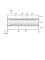
- the common electrode 102A has a length Lx in the direction along the X-axis direction and a length Ly in the direction along the Y-axis direction in a plan view.
- the length Lx and the length Ly are set to be optimal according to the frequency of the radio waves that the reflect array 100A targets.
- the common electrodes 102B, 102C, and 102D are also similar and have the same dimensions in a plan view.
- the interval Wy between the common electrodes 102A and 102B and the interval Wy between the common electrodes 102C and 102D shown in FIG. 7A are the same. That is, the common electrodes 102 are arranged at equal intervals in the unit cell array 20A.
- the interval Wy is usually designed to be smaller than the length Lx and the length Ly in order to arrange the common electrodes 102 at high density.
- the dimensions Lx and Ly of the common electrode 102 and the interval Wy between adjacent common electrodes are constant.
- the wiring length LA of the strip wiring 108A connecting common electrodes 102A and 102B is different from the wiring length LB of the strip wiring 108B connecting common electrodes 102C and 102D.
- the wiring length LA is the length along the center line of the wiring from the point where the strip wiring 108A is connected to common electrode 102A to the point where it is connected to common electrode 102B. The same is true for the wiring length LB.
- the reflect array 100A reflects vertically polarized waves having an amplitude in a direction parallel to one side of the common electrode 102 extending in the Y-axis direction
- the length Ly of the common electrode 102 is 1/2 the wavelength ⁇ of the vertically polarized waves.
- the length LA of the strip wiring 108A is the same as the length Ly of one side of the common electrode 102.
- the strip wiring 108A has a shape that is bent multiple times in a meander shape (or crank shape) in a planar view.
- the strip wiring 108A connecting the common electrodes 102A and 102B has a bent shape with multiple bending points between one end and the other end in a planar view.
- the wavelength ⁇ is the wavelength when the vertically polarized wave propagates in the air
- the apparent wavelength ⁇ g when propagating through the liquid crystal layer 106 (dielectric layer) is expressed as the following formula (1) based on the relative dielectric constant ⁇ s of the dielectric layer.
- the amplitude of the reflected wave is maximum. In other words, even if the length Ly of the common electrode 102 is constant, the amplitude of the reflected wave becomes smaller if the wiring length LA of the strip wiring 108A deviates from ⁇ g/2.
- the wiring length LB of the strip wiring 108B connecting the common electrodes 102C and 102D has a small bending width and is shorter than the length LA of the strip wiring 108A (LB ⁇ LA).
- the wiring length LB of the strip wiring 108B is smaller than ⁇ g/2. Therefore, the amplitude of the reflected waves of the common electrodes 102C and 102D is smaller than the amplitude of the common electrodes 102A and 102B.
- Figure 8 is a diagram explaining how the amplitude of the reflected wave is varied according to the length of the strip wiring 108 to conform to a Taylor distribution.
- the graph shown in the upper part shows the results of a simulation of the change in amplitude with respect to the length of the strip wiring.
- the graph in the lower part of Figure 8 shows the amplitude value for each unit cell calculated using the Taylor distribution formula.
- the Taylor distribution can be calculated as follows, according to Reference 1 (C. A. Balanis, "Antenna Theory", John Wiley & Sons, Inc., 1997, p. 358).
- the space factor SF() represents a sample of the Taylor pattern and can also be calculated using equation (7).
- the top graph in Figure 8 shows the results when the wiring length of the strip wiring is normalized by the amplitude of ⁇ g/2, and shows that the amplitude (dB) decreases as the wiring length becomes shorter. It also shows that the amplitude (dB) decreases when the wiring length becomes longer than ⁇ g/2.
- the amplitude of the reflected wave changes with the wiring length of the strip wiring 108 that connects the common electrodes, so by adjusting the wiring length of the strip wiring 108 within the unit cell array 20A, it is possible to match the amplitude distribution to a Taylor distribution.
- the wiring length of the strip wiring 108 so that the amplitude of the reflected wave from the unit cell 10A located on the outside is smaller than the amplitude of the reflected wave from the unit cell 10A located in the center of the unit cell array 20A, it is possible to fit the amplitude of the unit cell array 20A to a Taylor distribution.
- the size of the unit cell 10A (the size of the common electrode 102) is determined by the frequency (wavelength) of the target radio wave, so the number that can be arranged in one unit cell array 20A is limited.
- the reflect array 100A shown in this embodiment if the number of unit cells 10A is 10 or more, preferably 16 or more, the amplitude distribution can be fitted to a Taylor distribution.
- the shortest wiring length of the strip wiring 108 is the spacing Wy between the common electrodes 102, and it cannot be made shorter than that. However, in order to reduce the amplitude so as to fit the Taylor distribution, it may be necessary in the simulation to make the wiring length of the strip wiring 108 shorter than the spacing Wy between the common electrodes. In this case, by making the wiring length of the strip wiring longer than ⁇ g/2, it is possible to similarly reduce the amplitude of the radio waves reflected by the unit cell 10A.
- Figure 9 shows the result of calculating the array factor of a one-dimensional unit cell array.
- the array factor D( ⁇ ) is calculated as follows, according to Reference 2 (Kikuma Nobuyoshi, Fundamentals of Array Antennas, 2009 Microwave Exhibition Workshops and Exhibits, tutorial 3 (2009)).
- the unit cells 10A of the liquid crystal reflector 100A are arranged in a matrix as shown in Fig. 1, but here we consider a unit cell array 20A in which unit cells 10A1 to 10AK are arranged in the Y-axis direction as shown in Fig. 12.
- a radio wave is incident at an angle ⁇ with respect to the normal direction of the reflecting surface RS of the unit cell array 20A. If the radio wave arriving at the reference point of the reflecting surface RS is E0, the directivity function of the unit cell 10A is g( ⁇ ), and the radio wave incident on the unit cell array 20A is narrowband, the voltage induced in the k-th unit cell 10Ak is given by equation (8).
- ⁇ is the wavelength of the radio wave
- d k is the position of the kth unit cell measured from the reference point.
- the intensity E sum of the radio wave reflected by the unit cell array 20A is given by equations (9) and (10).
- a k and ⁇ k are the weight (the amplitude of each unit cell obtained by the Taylor distribution) and the phase shift amount multiplied by the k-th unit cell, and D( ⁇ ) is the array factor.
- graph A shows the directivity pattern due to the array factor when the wiring length of the strip wiring in the unit cell array 20A is successively shortened from the center to the edge so as to fit the Taylor distribution
- graph B shows the case where the wiring length of the strip wiring is constant in the unit cell array.
- the reflect array 100A has a configuration in which a bias voltage that controls the orientation of the liquid crystal layer 106 is applied to each of the unit cells 10A arranged in a matrix, and this allows the direction of reflection of radio waves to be controlled in the left-right, up-down, and diagonal directions. Therefore, by setting the length of the strip wiring 108 so that the amplitude of the reflected wave fits a Taylor distribution according to the direction in which the radio waves are reflected, the level of the side lobes in the reflected wave can be reduced.
- the reflect array 100A can suppress deterioration of the radiation pattern of the reflected wave by varying the length of the strip wiring 108 connecting the common electrodes 102 arranged in a matrix on the radio wave incident surface side from the center to the outer portion. Specifically, the length of the strip wiring 108 connecting along the arrangement of the common electrodes 102 arranged in a matrix in the X-axis direction or Y-axis direction is varied from the center to the outer portion of the arrangement, and the amplitude distribution of the reflected radio wave is fitted to a Taylor distribution, thereby reducing the side lobe level and suppressing deterioration of the radiation pattern of the reflected wave.
- This embodiment shows a reflect array 100B in which the configurations of the common electrode 102 and the bias electrode 104 are different from those of the first embodiment.
- the differences from the first embodiment will be mainly described, and overlapping parts will be omitted as appropriate.
- FIG. 10 shows a plan view of the reflect array 100B according to this embodiment.
- FIG. 11 shows a cross-sectional view corresponding to the area between C1 and C2 of the reflect array 100B shown in FIG. 10.
- FIG. 10 and FIG. 11 will be referred to as appropriate.
- the reflect array 100B includes a bias electrode 104 arranged on the radio wave incidence surface side, and a common electrode 102 arranged on the back side of the bias electrode 104 with a liquid crystal layer 106 sandwiched therebetween.
- the bias electrodes 104 are arranged in a matrix on the first substrate 150 side, and the common electrode 102 is arranged on the second substrate 152 side so as to overlap with the bias electrode 104.
- the common electrode 102 has a size that covers the entire bias electrodes 104 arranged in a matrix.
- the common electrode 102 has a size that overlaps with the entire area in which the bias electrodes 104 are arranged in a matrix.
- the reflect array 100B is composed of unit cells 10B in which the layered structure (which may also include the first substrate 150 and the second substrate 152) of the bias electrodes 104, the liquid crystal layer 106, and the common electrode 102 is the basic unit. It can also be said that the reflect array 100B has a configuration in which the unit cells 10B are arranged in a matrix.
- the common electrode 102 is large enough to cover the entire reflect array 100B so that it can be shared by multiple unit cells 10B.
- the multiple bias electrodes 104 are connected to adjacent ones along the X-axis or Y-axis direction by strip wiring 108.
- FIG. 10 shows an example in which multiple bias electrodes 104 are connected along the Y-axis direction by strip wiring 108.
- a bias signal that controls the alignment state of the liquid crystal layer 106 is applied to the bias electrodes 104. Therefore, a bias signal is applied to the bias electrodes 104 for each arrangement in the Y-axis direction.
- the first substrate 150 may be provided with a bias signal line driving circuit 118 that applies a bias signal to the bias electrodes 104 for each arrangement in the Y-axis direction.
- the strip wiring 108 connecting adjacent bias electrodes 104 has different lengths at the center and outside in the Y-axis direction arrangement of the bias electrodes 104, similar to the first embodiment.
- the length of the strip wiring 108 becomes shorter toward the outside compared to the length of the center portion in the Y-axis direction arrangement of the bias electrodes 104.
- the lengths of the strip wiring 108 are different in the unit cell array 20B so that the amplitude distribution of the reflected wave fits a Taylor distribution.
- the reflect array 100B according to this embodiment has a configuration in which a bias voltage that controls the orientation of the liquid crystal layer 106 is applied to the unit cell arrays 20B arranged in the Y-axis direction, and thus the reflection direction of radio waves can be controlled in one axis direction (left-right or up-down direction).
- FIG. 10 shows a configuration in which the unit cell arrays 20B arranged in the Y-axis direction are connected in series by strip wiring 108
- the reflect array 100B according to this embodiment is not limited to this configuration, and the unit cell arrays 20B arranged in the X-axis direction may be connected in series by strip wiring.
- the reflect array 100B of this embodiment has a configuration in which the lengths of the strip wiring 108 in the Y-axis direction of the bias electrodes 104 vary from the center to the outside so as to fit a Taylor distribution, thereby achieving the same effect as the first embodiment.
- 10A, 10B unit cell, 20A, 20B: unit cell array, 100A, 100B: reflect array, 102, 102A, 102B, 102C, 102D: common electrode, 104, 104A, 104B: bias electrode 104, 106: liquid crystal layer, 107: liquid crystal molecules, 108, 108A, 108B: strip wiring, 110: switching element, 112: selection signal line, 114: bias signal line, 116: selection signal line drive circuit, 118: bias signal line drive circuit, 120: terminal section, 122A: first alignment film, 122B: second alignment film, 124: semiconductor layer, 126: gate insulation layer, 128: gate electrode, 130: interlayer insulation layer, 132: planarization layer, 150: first substrate, 152: second substrate
Landscapes
- Physics & Mathematics (AREA)
- Electromagnetism (AREA)
- Aerials With Secondary Devices (AREA)
Priority Applications (3)
| Application Number | Priority Date | Filing Date | Title |
|---|---|---|---|
| JP2025510499A JPWO2024203461A1 (https=) | 2023-03-30 | 2024-03-15 | |
| CN202480015752.7A CN120917625A (zh) | 2023-03-30 | 2024-03-15 | 使用液晶材料的反射阵列 |
| US19/342,856 US20260024919A1 (en) | 2023-03-30 | 2025-09-29 | Intelligent reflecting surface |
Applications Claiming Priority (2)
| Application Number | Priority Date | Filing Date | Title |
|---|---|---|---|
| JP2023-055730 | 2023-03-30 | ||
| JP2023055730 | 2023-03-30 |
Related Child Applications (1)
| Application Number | Title | Priority Date | Filing Date |
|---|---|---|---|
| US19/342,856 Continuation US20260024919A1 (en) | 2023-03-30 | 2025-09-29 | Intelligent reflecting surface |
Publications (1)
| Publication Number | Publication Date |
|---|---|
| WO2024203461A1 true WO2024203461A1 (ja) | 2024-10-03 |
Family
ID=92905905
Family Applications (1)
| Application Number | Title | Priority Date | Filing Date |
|---|---|---|---|
| PCT/JP2024/010265 Ceased WO2024203461A1 (ja) | 2023-03-30 | 2024-03-15 | 液晶材料を用いたリフレクトアレイ |
Country Status (4)
| Country | Link |
|---|---|
| US (1) | US20260024919A1 (https=) |
| JP (1) | JPWO2024203461A1 (https=) |
| CN (1) | CN120917625A (https=) |
| WO (1) | WO2024203461A1 (https=) |
Citations (4)
| Publication number | Priority date | Publication date | Assignee | Title |
|---|---|---|---|---|
| JP2005303528A (ja) * | 2004-04-08 | 2005-10-27 | Hidekazu Ogawa | 電波偏波変換共振反射器、電波偏波変換共振反射装置、無線通信システム、金属対応無線icタグ装置、物品及びrfidシステム |
| JP2019530387A (ja) * | 2016-09-22 | 2019-10-17 | 華為技術有限公司Huawei Technologies Co.,Ltd. | ビーム・ステアリング・アンテナのための液晶調整可能メタサーフェス |
| WO2022244676A1 (ja) * | 2021-05-17 | 2022-11-24 | 株式会社ジャパンディスプレイ | 電波反射板および電波反射装置 |
| WO2022259790A1 (ja) * | 2021-06-09 | 2022-12-15 | 株式会社ジャパンディスプレイ | 電波反射板 |
-
2024
- 2024-03-15 JP JP2025510499A patent/JPWO2024203461A1/ja active Pending
- 2024-03-15 WO PCT/JP2024/010265 patent/WO2024203461A1/ja not_active Ceased
- 2024-03-15 CN CN202480015752.7A patent/CN120917625A/zh active Pending
-
2025
- 2025-09-29 US US19/342,856 patent/US20260024919A1/en active Pending
Patent Citations (4)
| Publication number | Priority date | Publication date | Assignee | Title |
|---|---|---|---|---|
| JP2005303528A (ja) * | 2004-04-08 | 2005-10-27 | Hidekazu Ogawa | 電波偏波変換共振反射器、電波偏波変換共振反射装置、無線通信システム、金属対応無線icタグ装置、物品及びrfidシステム |
| JP2019530387A (ja) * | 2016-09-22 | 2019-10-17 | 華為技術有限公司Huawei Technologies Co.,Ltd. | ビーム・ステアリング・アンテナのための液晶調整可能メタサーフェス |
| WO2022244676A1 (ja) * | 2021-05-17 | 2022-11-24 | 株式会社ジャパンディスプレイ | 電波反射板および電波反射装置 |
| WO2022259790A1 (ja) * | 2021-06-09 | 2022-12-15 | 株式会社ジャパンディスプレイ | 電波反射板 |
Also Published As
| Publication number | Publication date |
|---|---|
| JPWO2024203461A1 (https=) | 2024-10-03 |
| US20260024919A1 (en) | 2026-01-22 |
| CN120917625A (zh) | 2025-11-07 |
Similar Documents
| Publication | Publication Date | Title |
|---|---|---|
| US20240128652A1 (en) | Intelligent reflecting surface | |
| US12117698B2 (en) | Intelligent reflecting surface and intelligent reflecting device | |
| US20240243484A1 (en) | Reflect array | |
| US20250015508A1 (en) | Reflect array | |
| US20240364008A1 (en) | Reflect array | |
| US20250149800A1 (en) | Reflecting device | |
| US20250023252A1 (en) | Reflecting device having liquid crystal material | |
| WO2024203461A1 (ja) | 液晶材料を用いたリフレクトアレイ | |
| US12578599B2 (en) | Reflecting device having liquid crystal material | |
| US20200326607A1 (en) | Dielectric travelling wave time domain beamformer | |
| US20260003234A1 (en) | Intelligent reflecting surface | |
| US20250379367A1 (en) | Intelligent reflecting surface | |
| US20250266865A1 (en) | Intelligent reflecting surface | |
| US20250219681A1 (en) | Intelligent reflecting surface | |
| US20250210880A1 (en) | Reflecting device | |
| US20250309554A1 (en) | Intelligent reflecting surface | |
| US20260011928A1 (en) | Intelligent reflecting surface | |
| US20250379366A1 (en) | Intelligent reflecting surface and reflecting device | |
| US20250093708A1 (en) | Reflecting device | |
| WO2025052894A1 (ja) | 電波反射装置及びこれを含む電波反射システム | |
| WO2025027981A1 (ja) | 電波反射装置の検査装置、およびその検査方法 | |
| WO2024070939A1 (ja) | 電波反射装置 | |
| WO2026083760A1 (ja) | 電波反射装置の駆動方法 | |
| CN120226211A (zh) | 电波反射装置 |
Legal Events
| Date | Code | Title | Description |
|---|---|---|---|
| 121 | Ep: the epo has been informed by wipo that ep was designated in this application |
Ref document number: 24779589 Country of ref document: EP Kind code of ref document: A1 |
|
| WWE | Wipo information: entry into national phase |
Ref document number: 202480015752.7 Country of ref document: CN |
|
| ENP | Entry into the national phase |
Ref document number: 2025510499 Country of ref document: JP Kind code of ref document: A |
|
| WWE | Wipo information: entry into national phase |
Ref document number: 2025510499 Country of ref document: JP |
|
| NENP | Non-entry into the national phase |
Ref country code: DE |
|
| WWP | Wipo information: published in national office |
Ref document number: 202480015752.7 Country of ref document: CN |
|
| 122 | Ep: pct application non-entry in european phase |
Ref document number: 24779589 Country of ref document: EP Kind code of ref document: A1 |