WO2024203256A1 - 光検出装置及び電子機器 - Google Patents
光検出装置及び電子機器 Download PDFInfo
- Publication number
- WO2024203256A1 WO2024203256A1 PCT/JP2024/009442 JP2024009442W WO2024203256A1 WO 2024203256 A1 WO2024203256 A1 WO 2024203256A1 JP 2024009442 W JP2024009442 W JP 2024009442W WO 2024203256 A1 WO2024203256 A1 WO 2024203256A1
- Authority
- WO
- WIPO (PCT)
- Prior art keywords
- region
- trench isolation
- insulating
- semiconductor
- view
- Prior art date
- Legal status (The legal status is an assumption and is not a legal conclusion. Google has not performed a legal analysis and makes no representation as to the accuracy of the status listed.)
- Ceased
Links
Images























Classifications
-
- H—ELECTRICITY
- H10—SEMICONDUCTOR DEVICES; ELECTRIC SOLID-STATE DEVICES NOT OTHERWISE PROVIDED FOR
- H10F—INORGANIC SEMICONDUCTOR DEVICES SENSITIVE TO INFRARED RADIATION, LIGHT, ELECTROMAGNETIC RADIATION OF SHORTER WAVELENGTH OR CORPUSCULAR RADIATION
- H10F39/00—Integrated devices, or assemblies of multiple devices, comprising at least one element covered by group H10F30/00, e.g. radiation detectors comprising photodiode arrays
- H10F39/10—Integrated devices
- H10F39/12—Image sensors
-
- H—ELECTRICITY
- H10—SEMICONDUCTOR DEVICES; ELECTRIC SOLID-STATE DEVICES NOT OTHERWISE PROVIDED FOR
- H10W—GENERIC PACKAGES, INTERCONNECTIONS, CONNECTORS OR OTHER CONSTRUCTIONAL DETAILS OF DEVICES COVERED BY CLASS H10
- H10W10/00—Isolation regions in semiconductor bodies between components of integrated devices
-
- H—ELECTRICITY
- H10—SEMICONDUCTOR DEVICES; ELECTRIC SOLID-STATE DEVICES NOT OTHERWISE PROVIDED FOR
- H10W—GENERIC PACKAGES, INTERCONNECTIONS, CONNECTORS OR OTHER CONSTRUCTIONAL DETAILS OF DEVICES COVERED BY CLASS H10
- H10W10/00—Isolation regions in semiconductor bodies between components of integrated devices
- H10W10/01—Manufacture or treatment
Definitions
- This technology (the technology disclosed herein) relates to photodetection devices and electronic devices, and in particular to photodetection devices and electronic devices that are compatible with miniaturization.
- trench isolation may be used as an isolation structure that divides semiconductor regions (for example, Patent Document 1).
- the aim of this technology is to provide photodetection devices and electronic devices that are compatible with miniaturization.
- a photodetector includes a first semiconductor layer having a plurality of cell regions arranged in a matrix along the row and column directions in a planar view, one surface of which is an element formation surface and the other surface of which is a light incidence surface, a trench isolation wall separating the cell regions, and an insulating region made of an insulating material and having a dimension in the width direction greater than the dimension in the width direction of the trench isolation wall in a planar view, the cell region including a photoelectric conversion unit and the first semiconductor region provided on a surface of the insulating region opposite to the surface of the trench isolation wall.
- An electronic device includes the above-mentioned light detection device and an optical system that focuses image light from a subject on the above-mentioned light detection device.
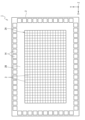
- 1 is a chip layout diagram showing a configuration example of a photodetector according to a first embodiment of the present technology.
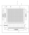
- 1 is a block diagram showing a configuration example of a light detection device according to a first embodiment of the present technology.
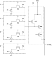
- 2 is an equivalent circuit diagram of a pixel of the photodetection device according to the first embodiment of the present technology.
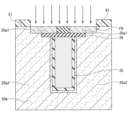
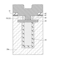
- 1 is a longitudinal sectional view showing a cross-sectional configuration of a pixel included in a photodetection device according to a first embodiment of the present technology.
- 4B is a cross-sectional view showing a cross-sectional configuration when viewed in cross section along the line BB in FIG. 4A.
- FIG. 4B is a cross-sectional view showing a cross-sectional configuration when viewed in cross section along the CC cutting line in FIG. 4A.
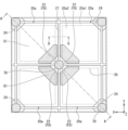
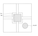
- 1 is an explanatory diagram showing the positional relationship between an electrode, a charge accumulation region, a contact region, a first semiconductor region, and a second semiconductor region on the first surface side of a first semiconductor layer according to a first embodiment.
- FIG. FIG. 4E is a partially enlarged view showing a portion of FIG. 4D.
- 4E is a longitudinal sectional view showing an enlarged portion of the sectional configuration when viewed in cross section along the AA cutting line in FIG. 4D.
- 4D is a longitudinal cross-sectional view showing a cross-sectional configuration when viewed in cross section along the line DD in FIG. 4D.
- FIG. 2 is a plan view of the body portion according to the first embodiment.
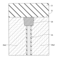
- 5A to 5C are cross-sectional views illustrating steps of a manufacturing method for a light detection device according to the first embodiment of the present technology.
- 5B is a cross-sectional view showing a process subsequent to FIG. 5A.
- 5B is a cross-sectional view showing a process subsequent to FIG. 5B.
- 5D is a cross-sectional view showing a process subsequent to FIG. 5C.
- 5D is a cross-sectional view showing a process subsequent to FIG. 5D.
- 5E is a cross-sectional view showing a process subsequent to FIG. 5E. 5F
- FIG. 5G FIG. 5H is a cross-sectional view showing a process subsequent to FIG. 5H. 5I.
- FIG. 4 is a longitudinal sectional view showing a cross-sectional configuration of an electrode and a charge accumulation region of a photodetector according to a comparative example.
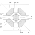
- FIG. FIG. 1 is an explanatory diagram showing the positional relationship between an electrode, a charge accumulation region, a first semiconductor region, and a second semiconductor region on the first surface side of a first semiconductor layer of a photodetector according to a first modified example of the first embodiment of the present technology.
- 7B is a longitudinal cross-sectional view showing a cross-sectional configuration when viewed in cross section along the E-E cutting line in FIG. 7A.
- 10A to 10C are cross-sectional views illustrating steps of a manufacturing method for a light detection device according to a first modified example of the first embodiment of the present technology.
- 8B is a cross-sectional view showing a process subsequent to FIG. 8A.
- 8C is a plan view showing the planar shape of an opening in a resist pattern used in the process shown in FIG. 8B.
- 11 is an explanatory diagram showing a state in which silicon is epitaxially grown only on corners of a cell region in a photodetector according to a first modified example of a first embodiment of the present technology;
- FIG. 11 is an explanatory diagram showing, in a plan view, a gate electrode and an electrode included in a photodetector 1 according to a second modified example of the first embodiment.
- FIG. 13 is an explanatory diagram showing, in a plan view, a gate electrode and an electrode included in a photodetector 1 according to a third modified example of the first embodiment.
- FIG. 13 is an explanatory diagram showing, in plan view, a gate electrode and an electrode included in a photodetector 1 according to a fourth modified example of the first embodiment.
- FIG. 13 is an explanatory diagram showing, in plan view, electrodes included in a light detection device 1 according to a fifth modified example of the first embodiment.
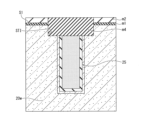
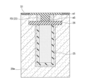
- FIG. 13 is a longitudinal cross-sectional view showing a cross-sectional configuration of an electrode, a charge accumulation region, and an insulating region in a plane along a cutting line that crosses a body portion in a photodetector according to a second embodiment of the present technology.
- FIG. 13 is an explanatory diagram showing the positional and dimensional relationships between a charge accumulation region and an electrode in a plan view in a photodetector according to a second embodiment of the present technology;
- FIG. 7A to 7C are cross-sectional views illustrating steps of a method for manufacturing a light detection device according to a second embodiment of the present technology.
- 15B is a cross-sectional view showing a process subsequent to FIG. 15A.
- 15B is a cross-sectional view showing a process subsequent to FIG. 15B.
- 15D is a cross-sectional view showing a process subsequent to FIG. 15C.
- 15D is a cross-sectional view showing a process subsequent to FIG. 15D.
- 10 is an explanatory diagram showing the positional relationship in a plan view of a gate electrode and a charge accumulation region of a photodetector according to a comparative example;
- FIG. 11 is an explanatory diagram showing a positional relationship, in a plan view, between a gate electrode and a charge accumulation region included in a photodetector according to a second embodiment of the present technology;
- FIG. 13 is an explanatory diagram showing a positional relationship, in a plan view, between a gate electrode and a charge accumulation region included in a photodetector according to a first modified example of a second embodiment of the present technology
- FIG. 13 is an explanatory diagram showing a positional relationship, in a plan view, between a gate electrode and a charge accumulation region included in a photodetector according to a first modified example of a second embodiment of the present technology
- FIG. 13A to 13C are cross-sectional views illustrating steps of a manufacturing method for a light detection device according to a second modification of the second embodiment of the present technology.
- 19B is a cross-sectional view showing a process subsequent to FIG. 19A.
- FIG. 13 is a longitudinal cross-sectional view showing a cross-sectional configuration of a phase difference detection unit included in a photodetection device according to a third embodiment of the present technology.
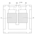
- FIG. 13 is an explanatory diagram showing a positional relationship between a first semiconductor region and a first trench isolation wall on a first surface side of a phase difference detection unit according to a third embodiment of the present technology;
- FIG. 20C is a longitudinal cross-sectional view showing the cross-sectional configuration when viewed in cross-section along the line G-G in FIG. 20B.
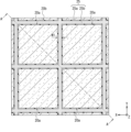
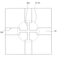
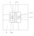
- 13 is an explanatory diagram showing a configuration on a first surface side of four phase difference detection units arranged in two rows and two columns according to a third embodiment of the present technology.
- FIG. 13 is an explanatory diagram showing a configuration on a first surface side of four phase difference detection units arranged in two rows and two columns according to a third embodiment of the present technology.
- FIG. 13 is a plan view showing a resist pattern used when forming a groove by etching from the first surface S1 side in a manufacturing method for a photodetector according to a third embodiment of the present technology.
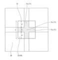
- FIG. 13 shows the shape and position in a plan view of an insulating region formed in a manufacturing method for a photodetector according to a third embodiment of the present technology.
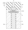
- 13 is a vertical cross-sectional view showing a first semiconductor region formed by epitaxial growth in a method for manufacturing a photodetector according to a third embodiment of the present technology.
- FIG. 1 is a longitudinal sectional view showing a sectional configuration of a pixel included in a photodetection device according to a comparative example.
- FIG. 13 is an explanatory diagram showing a configuration on a first surface side of four phase difference detection units arranged in two rows and two columns according to a first modified example of the third embodiment of the present technology
- FIG. 25B is a longitudinal cross-sectional view showing the cross-sectional configuration when viewed in cross-section along the line G-G in FIG. 25A.
- 13 is a plan view showing a resist pattern used when performing etch-back to remove unnecessary portions of an insulating film to obtain an insulating region in a manufacturing method for a photodetector according to a first modified example of a third embodiment of the present technology
- FIG. 25B is a longitudinal cross-sectional view showing the cross-sectional configuration when viewed in cross-section along the line G-G in FIG. 25A
- 13 is a plan view showing a resist pattern used when performing etch-back to remove unnecessary portions of an insulating film to obtain an insulating region in a manufacturing method for a photodetector according to a first modified example of
- FIG. 13 is an explanatory diagram showing a planar configuration on the first surface S1 side of a charge accumulation region of a photodetector according to a second modification of the third embodiment of the present technology
- FIG. 13 is an explanatory diagram showing a planar configuration on the first surface S1 side of a charge accumulation region of a photodetector according to a third modification of the third embodiment of the present technology
- FIG. FIG. 1 is a block diagram showing an example of a schematic configuration of an electronic device.
- the embodiments shown below are examples of devices and methods for embodying the technical ideas of the present technology, and the technical ideas of the present technology do not specify the materials, shapes, structures, arrangements, etc. of the components as described below.
- the technical ideas of the present technology can be modified in various ways within the technical scope defined by the claims.
- the definitions of directions such as up and down in the following explanation are merely for the convenience of explanation and do not limit the technical ideas of the present disclosure. For example, if an object is rotated 90 degrees and observed, up and down are converted to left and right and read, and of course if it is rotated 180 degrees and observed, up and down are read inverted.
- CMOS complementary metal oxide semiconductor
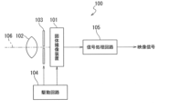
- the photodetection device 1 As shown in Fig. 1, the photodetection device 1 according to the first embodiment of the present technology is mainly composed of a semiconductor chip 2 having a rectangular two-dimensional planar shape when viewed in a plan view. That is, the photodetection device 1 is mounted on the semiconductor chip 2. As shown in Fig. 29, the photodetection device 1 takes in image light (incident light 106) from a subject via an optical system (optical lens) 102, converts the amount of incident light 106 formed on an imaging surface into an electrical signal on a pixel-by-pixel basis, and outputs the electrical signal as a pixel signal.
- image light incident light 106
- optical system optical lens
- the semiconductor chip 2 on which the light detection device 1 is mounted has a square pixel area 2A provided in the center in a two-dimensional plane including the X and Y directions that intersect with each other, and a peripheral area 2B provided outside the pixel area 2A so as to surround the pixel area 2A.
- the pixel area 2A is a light receiving surface that receives light collected by an optical system 102 shown in FIG. 29, for example.
- a plurality of pixels 3 are arranged in a matrix in a two-dimensional plane including the X and Y directions.
- the pixels 3 are repeatedly arranged in each of the X direction (e.g., row direction) and Y direction (e.g., column direction) that intersect with each other in the two-dimensional plane.
- the X direction and the Y direction are orthogonal to each other as an example.
- the direction orthogonal to both the X direction and the Y direction is the Z direction (thickness direction, stacking direction).
- the direction perpendicular to the Z direction is the horizontal direction.
- a plurality of bonding pads 14 are arranged in the peripheral region 2B.
- Each of the plurality of bonding pads 14 is arranged, for example, along each of the four sides of the semiconductor chip 2 in a two-dimensional plane.
- Each of the plurality of bonding pads 14 is an input/output terminal used when electrically connecting the semiconductor chip 2 to an external device.
- the semiconductor chip 2 includes a logic circuit 13.
- the logic circuit 13 includes a vertical drive circuit 4, a column signal processing circuit 5, a horizontal drive circuit 6, an output circuit 7, and a control circuit 8.
- the logic circuit 13 is configured of a CMOS (Complementary MOS) circuit having, as field effect transistors, for example, an n-channel conductivity type MOSFET (Metal Oxide Semiconductor Field Effect Transistor) and a p-channel conductivity type MOSFET.
- CMOS Complementary MOS
- the vertical drive circuit 4 is composed of, for example, a shift register.
- the vertical drive circuit 4 sequentially selects the desired pixel drive lines 10, supplies pulses to the selected pixel drive lines 10 for driving the pixels 3, and drives each pixel 3 row by row. That is, the vertical drive circuit 4 sequentially selects and scans each pixel 3 in the pixel area 2A vertically row by row, and supplies pixel signals from the pixels 3 based on signal charges generated by the photoelectric conversion elements of each pixel 3 according to the amount of light received to the column signal processing circuit 5 via the vertical signal lines 11.
- the column signal processing circuit 5 is arranged, for example, for each column of pixels 3, and performs signal processing such as noise removal for each pixel column on the signals output from one row of pixels 3.
- the column signal processing circuit 5 performs signal processing such as CDS (Correlated Double Sampling) and AD (Analog Digital) conversion to remove pixel-specific fixed pattern noise.
- a horizontal selection switch (not shown) is provided at the output stage of the column signal processing circuit 5 and connected between it and the horizontal signal line 12.
- the horizontal drive circuit 6 is composed of, for example, a shift register.
- the horizontal drive circuit 6 sequentially outputs horizontal scanning pulses to the column signal processing circuits 5, thereby selecting each of the column signal processing circuits 5 in turn, and causing each of the column signal processing circuits 5 to output a pixel signal that has been subjected to signal processing to the horizontal signal line 12.
- the output circuit 7 processes and outputs pixel signals sequentially supplied from each of the column signal processing circuits 5 through the horizontal signal line 12.
- the signal processing may include buffering, black level adjustment, column variation correction, various types of digital signal processing, etc.
- the control circuit 8 generates clock signals and control signals that serve as the basis for the operation of the vertical drive circuit 4, column signal processing circuit 5, horizontal drive circuit 6, etc., based on the vertical synchronization signal, horizontal synchronization signal, and master clock signal. The control circuit 8 then outputs the generated clock signals and control signals to the vertical drive circuit 4, column signal processing circuit 5, horizontal drive circuit 6, etc.
- ⁇ Pixels> 3 is an equivalent circuit diagram showing an example of a configuration of a pixel 3.
- a plurality of pixels 3 share one readout circuit 15. More specifically, four pixels 3 share one readout circuit 15.
- Each pixel 3 includes a photoelectric conversion element PD, a transfer transistor TR that transfers a signal charge photoelectrically converted by the photoelectric conversion element PD to a charge accumulation region FD, and a charge accumulation region (floating diffusion) FD.
- the readout circuit 15 is connected to the rear stage of the charge accumulation region FD.
- the photoelectric conversion element PD generates a signal charge according to the amount of light received.
- the photoelectric conversion element PD also temporarily accumulates (holds) the generated signal charge.
- the cathode side of the photoelectric conversion element PD is electrically connected to the source region of the transfer transistor TR, and the anode side is electrically connected to a reference potential line (e.g., ground).
- a photodiode is used as the photoelectric conversion element PD.
- the drain region of the transfer transistor TR is electrically connected to the charge storage region FD.
- the gate electrode of the transfer transistor TR is electrically connected to the transfer transistor drive line of the pixel drive line 10 (see FIG. 2).
- the charge storage region FD temporarily stores and holds the signal charge transferred from the photoelectric conversion element PD via the transfer transistor TR.
- the readout circuit 15 reads out the signal charge stored in the charge storage region FD and outputs a pixel signal based on the signal charge.
- the readout circuit 15 includes, but is not limited to, an amplification transistor AMP, a selection transistor SEL, and a reset transistor RST as pixel transistors.
- These transistors are configured as MOSFETs having, for example, a gate insulating film made of a silicon oxide film (SiO 2 film), a gate electrode, and a pair of main electrode regions functioning as a source region and a drain region.
- these transistors may be MISFETs (Metal Insulator Semiconductor FETs) whose gate insulating film is made of a silicon nitride film (Si 3 N 4 film) or a laminated film such as a silicon nitride film and a silicon oxide film.
- MISFETs Metal Insulator Semiconductor FETs
- the source region of the amplification transistor AMP is electrically connected to the drain region of the selection transistor SEL, and the drain region is electrically connected to the power supply line Vdd and the drain region of the reset transistor.
- the gate electrode of the amplification transistor AMP is electrically connected to the charge storage region FD and the source region of the reset transistor RST.
- the source region of the selection transistor SEL is electrically connected to the vertical signal line 11 (VSL), and the drain is electrically connected to the source region of the amplification transistor AMP.
- the gate electrode of the selection transistor SEL is electrically connected to the selection transistor drive line of the pixel drive line 10 (see FIG. 2).
- the source region of the reset transistor RST is electrically connected to the charge storage region FD and the gate electrode of the amplification transistor AMP, and the drain region is electrically connected to the power supply line Vdd and the drain region of the amplification transistor AMP.
- the gate electrode of the reset transistor RST is electrically connected to the reset transistor drive line of the pixel drive line 10 (see FIG. 2).
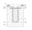
- Fig. 4A is a cross-sectional view showing a cross-sectional configuration when viewed in cross section along the A-A cutting line in Fig. 4B and Fig. 4C.
- the photodetector 1 semiconductor chip 2 has a laminated structure in which, for example, a first semiconductor layer 20 having one surface as a first surface S1 and the other surface as a second surface S2, a first wiring layer 30, a second semiconductor layer 40, a second wiring layer 50, and a third semiconductor layer (not shown) are laminated in that order.
- the photodetector 1 (semiconductor chip 2) has a light incident surface side laminate 60 on the second surface S2 side.
- the first semiconductor layer 20 is made of a semiconductor substrate.
- the first semiconductor layer 20 is mainly made of, for example, a single crystal silicon (Si) substrate, although it is not limited thereto.
- the first surface S1 may be called an element forming surface or a main surface, and the second surface S2 may be called a light incident surface or a back surface.
- a plurality of cell regions 20a arranged in a matrix shape along the row direction and the column direction in a plan view are provided in the portion corresponding to the pixel region 2A of the first semiconductor layer 20, a plurality of cell regions 20a arranged in a matrix shape along the row direction and the column direction in a plan view are provided.
- the cell region 20a is provided for each pixel 3.
- an island-shaped cell region 20a partitioned by an isolation region 20b is provided for each pixel 3.
- the number of pixels 3 is not limited to that shown in FIG. 4A.
- a semiconductor region 21 and a semiconductor region 22 are configured in the cell region 20a.
- the semiconductor region 21 is a first conductivity type (e.g., p-type) or a true semiconductor (i-type), and in this embodiment, it will be described as the first conductivity type (e.g., p-type).
- the semiconductor region 22 is a second conductivity type (e.g., n-type).
- the photoelectric conversion element PD shown in FIG. 3 is configured in the cell region 20a, which performs photoelectric conversion of incident light and generates a signal charge.
- the semiconductor region 22 may be referred to as a photoelectric conversion section 22.
- the cell region 20a includes a semiconductor region 23 of a second conductivity type (e.g., n-type) and a semiconductor region 24 of a first conductivity type (e.g., p-type).
- the semiconductor region 23 corresponds to the charge storage region FD shown in FIG. 3.
- the semiconductor region 23 is referred to as the charge storage region FD.
- the charge storage region FD is a diffusion region having a higher impurity concentration than the photoelectric conversion section 22.
- the semiconductor region 24 is a contact region to which wiring for fixing the semiconductor region 21 to a reference potential is connected.
- the semiconductor region 24 is referred to as the contact region 24.
- the contact region 24 is a diffusion region having a higher impurity concentration than the semiconductor region 21.
- the charge storage region FD and the contact region 24 are provided at a position closer to the first surface S1 in the thickness direction, and may face the first surface S1.
- the cell region 20a also includes a first semiconductor region 20a1 shown in FIG. 4D. The first semiconductor region 20a1 will be described in detail later.
- a transistor T1 is provided in the cell region 20a.
- the transistor T1 is provided at a position close to the first surface S1 of the first semiconductor layer 20.
- the transistor T1 is, for example, the transfer transistor TR shown in FIG. 3.
- the transistor T1 will be referred to as the transfer transistor T1.
- the isolation region 20b has an isolation structure that separates the cell regions 20a from each other.
- the isolation structure may be a known structure such as an impurity isolation structure or a trench isolation wall.
- the isolation structure is described as being the trench isolation wall 25 shown in FIG. 4A.
- the trench isolation wall 25 is a trench structure in which a trench FTI is formed in the isolation region 20b of the first semiconductor layer 20 along the thickness direction and an isolation material is embedded in the trench FTI.
- the trench isolation wall 25 is, for example, an FTI (Full Trench Isolation) structure in which an isolation material is embedded in a trench FTI extending from the first surface S1 to the second surface S2 along the thickness direction.
- FTI Frull Trench Isolation
- the isolation material may be a known material such as an insulating film or a metal.
- the trench isolation wall 25 includes polysilicon 25b and an insulating film 25a.
- the insulating film 25a insulates between the polysilicon 25b and the semiconductor region 21.
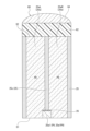
- FIG. 4B is a cross-sectional view showing a cross-sectional configuration when viewed along the B-B cutting line in FIG. 4A. As shown in FIG. 4B, the trench isolation wall 25 has a portion extending along the row direction and the thickness direction and a portion extending along the column direction and the thickness direction. The portion extending along the row direction and the thickness direction intersects with the portion extending along the column direction and the thickness direction.
- the portion where the portion extending along the row direction and the thickness direction intersects with the portion extending along the column direction and the thickness direction is called an intersection region.
- the trench isolation wall 25 is provided in a lattice shape along the row direction and the column direction in a plan view.
- the dimension along the width direction of the trench isolation wall 25 is W1.
- the charge storage region FD is provided, for example, at a corner of the cell region 20a in plan view, though this is not limited thereto. More specifically, in the four cell regions 20a in two rows and two columns that share one readout circuit 15, the charge storage region FD is provided at mutually opposing corners of the cell region 20a in plan view. Also, the contact region 24 is provided, for example, at a corner of the cell region 20a in plan view, though this is not limited thereto. More specifically, the contact region 24 is provided at a corner of the cell region 20a that is different from the corner where the charge storage region FD is provided. In the four cell regions 20a in two rows and two columns, the contact region 24 is provided at mutually opposing corners of the cell region 20a in plan view.
- FIG. 4A an insulating region 26 made of an insulating material is provided at the end of the trench isolation wall 25 closer to the first surface S1.
- One surface (the surface closer to the second surface S2) of the insulating region 26 is in contact with the end of the trench isolation wall 25 closer to the first surface S1.
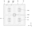
- FIG. 4C is a cross-sectional view showing a cross-sectional configuration when viewed in cross section along the C-C cutting line in FIG. 4A.
- the insulating region 26 extends in the row direction and the column direction so as to separate the cell regions 20a from each other in a plan view.
- the insulating region 26 is provided along the trench isolation wall 25 and overlaps the trench isolation wall 25. More specifically, in a plan view, the entire trench isolation wall 25 overlaps the insulating region 26. In addition, the insulating region 26 is provided in the entire area where the trench isolation wall 25 is provided in a plan view.
- the dimension W2 of the insulating region 26 along the width direction is larger than the dimension W1 along the width direction of the trench isolation wall 25 (W2>W1).
- the insulating material constituting the insulating region 26 is not limited to this, but may be silicon oxide (SiO 2 ) or the like.
- Fig. 4G is a longitudinal sectional view showing the cross-sectional configuration when viewed along the D-D cutting line in Fig. 4D.
- narrow insulating regions 27 extending in the row and column directions are provided on the surface of insulating region 26 closer to first surface S1 so as to separate cell regions 20a from each other.
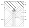
- FIG. 4F is a vertical cross-sectional view showing an enlarged portion of the cross-sectional configuration when viewed in a plane along the A-A cutting line in FIG. 4D.
- the narrow insulating region 27 is removed and an electrode 70 is provided.
- the position where the contact region 24 is provided in a plan view has a similar configuration, so illustration and description may be omitted.
- the charge accumulation region FD will be used as an example for description.
- the charge accumulation region FD can be read as the contact region 24.
- the first semiconductor region 20a1 is provided between the insulating region 26 and the first surface S1 in the thickness direction, with one surface in contact with the surface of the insulating region 26 closer to the first surface S1 and the other surface facing the first surface S1. More specifically, the first semiconductor region 20a1 is a portion of the cell region 20a that is provided on the surface of the insulating region 26 closer to the first surface S1 and that overlaps with the insulating region 26 in a plan view.
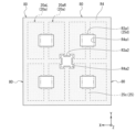
- FIG. 4D is a diagram showing the cell region 20a when the first semiconductor layer 20 is viewed from the first surface S1 side.
- a first semiconductor region 20a1 is provided for each cell region 20a. More specifically, the first semiconductor region 20a1 is provided over the entire edge of the cell region 20a when observed from the first surface S1 side in a plan view.
- the first semiconductor regions 20a1 of adjacent cell regions 20a are provided with a gap between them and are not in contact with each other.
- the portion of the cell region 20a that is inside the insulating region 26 in a plan view is called the second semiconductor region 20a2 and is distinguished from the first semiconductor region 20a1.
- the charge storage region FD is configured in a region of the cell region 20a that includes at least a portion of the first semiconductor region 20a1. More specifically, the charge storage region FD is configured in a region of the cell region 20a that includes both the first semiconductor region 20a1 and the second semiconductor region 20a2.
- the photodetector 1 has an electrode 70.
- the electrode 70 includes an electrode 70 electrically connected to the charge accumulation region FD and an electrode 70 electrically connected to the contact region 24, but since both electrodes 70 have the same configuration, the electrode 70 electrically connected to the charge accumulation region FD will be described here as an example.
- the electrode 70 is an electrode that connects the wiring connected to the readout circuit 15 and the charge storage region FD of each pixel 3, and one electrode 70 is provided for multiple (four in this embodiment) pixels 3 that share one readout circuit 15.
- the electrode 70 has a body 71 and a head 72 whose one surface is connected to one end of the body 71.
- the other end of the body 71 is in contact with the surface of the insulating region 26 closer to the first surface S1 (i.e., the surface opposite the trench isolation wall 25), and the electrode 70 is in contact with the charge storage region FD via the side of the body 71 and one surface of the head 72 (the surface on the first semiconductor layer 20 side).
- the side of the body 71 and one surface of the head 72 of the electrode 70 are in contact with the portion of the first semiconductor region 20a1 in which the charge storage region FD is configured. However, this does not exclude that the side of the body 71 of the electrode 70 and one surface of the head 72 are in contact with the second semiconductor region 20a2 in which the charge storage region FD is formed.
- the side of the body 71 is a surface that connects one end of the body 71 to the other end.
- the other surface of the head 72 faces the first wiring layer 30 and is connected to the wiring 32.
- the head 72 extends in a plate shape along the horizontal direction, and the area of one surface of the head 72 is larger than the area of one end of the body 71.
- the head 72 can extend horizontally from the body 71 in a vertical cross-sectional view and contact the charge storage region FD.
- the electrode 70 is provided at a position where the charge storage regions FD face each other in a plan view.
- the body 71 separates (partitions) between the cell regions 20a, more specifically, between the charge storage regions FD, as shown in FIG. 4E.
- One electrode 70 contacts multiple charge storage regions FD that share one readout circuit 15. More specifically, one electrode 70 contacts multiple (four in this embodiment) charge storage regions FD provided in different cell regions 20a.
- the body 71 has a first extension portion 71x extending along the row direction and the thickness direction, and a second extension portion 71y extending along the column direction and the thickness direction.
- the first extension portion 71x and the second extension portion 71y intersect at the center, and more specifically, are perpendicular to each other. This intersecting portion is called the intersecting portion 71c.
- a charge storage region FD contacts each of the four recessed corners of the body 71 formed by the first extension portion 71x and the second extension portion 71y.
- FIG. 4F is a vertical cross-sectional view showing a part of the cross-sectional configuration when viewed in a plane along the A-A cutting line in FIG. 4D. If the distance between two charge storage regions FD facing each other via the body 71 in the vertical cross-sectional view of FIG. 4F is b, and the dimension along the horizontal direction of the insulating region 26 is a, then the distance b is smaller than the dimension a (b ⁇ a). If the dimension along the horizontal direction of the head 72 in the vertical cross-sectional view is c, then the dimension c is greater than or equal to the distance b (b ⁇ c). If the dimension c is equal to the distance b, then the head 72 has no portion that protrudes beyond the body 71.
- distance b, dimension a, and dimension c are the same even when intersection 71c is viewed in cross section in a plane along a cutting line different from the A-A cutting line.
- the relationship between distance b, dimension a, and dimension c is also the same in the cross-sectional configuration when light detection device 1 is viewed in longitudinal section in a plane along a cutting line that does not cross intersection 71c in plan view but crosses first extension portion 71x or second extension portion 71y.
- the material constituting the electrode 70 is a known conductive material.
- the material constituting the electrode 70 may be a known metal material such as aluminum (Al), copper (Cu), or tungsten (W).
- the electrode 70 is described as being made of polysilicon (Poly-Si).
- the electrode 70 electrically connected to the contact region 24 may be called a contact electrode 70 to be distinguished from the electrode 70 electrically connected to the charge storage region FD.
- the body 71 and head 72 of the contact electrode 70 are called the contact body 71 and contact head 72.
- a transfer transistor T1 is provided for each cell region 20a.
- the transfer transistor T1 is a transistor capable of transferring signal charges generated in the photoelectric conversion unit 22 to the charge accumulation region FD. For example, when the transfer transistor T1 is turned on, conduction is established between the photoelectric conversion unit 22 and the charge accumulation region FD, and the signal charges are transferred to the charge accumulation region FD. When the transfer transistor T1 is turned off, conduction between the photoelectric conversion unit 22 and the charge accumulation region FD is interrupted.
- the transfer transistor T1 has a gate electrode G1.
- the gate electrode G1 has a columnar first portion G1a that is embedded in the cell region 20a and extends in the thickness direction, and a second portion G1b that is provided in the first wiring layer 30, is connected to an end of the first portion G1a closer to the first surface S1, and extends horizontally in a plate-like shape.
- the gate insulating film that insulates the first portion G1a from the cell region 20a is omitted.
- the first wiring layer 30 is a multi-layer wiring layer in which one surface is in contact with the first semiconductor layer 20 and the other surface is in contact with the second wiring layer 50.
- the first wiring layer 30 has, for example, an insulating film 31 and wiring 32 provided in the insulating film 31, but is not limited thereto.
- the wiring 32 includes vertical wiring that mainly extends in the thickness direction and horizontal wiring that mainly extends in the horizontal direction.
- the insulating film 31 is configured by laminating multiple layers of known insulating films such as silicon oxide (SiO 2 ) films, silicon nitride (Si 3 N 4 ) films, and silicon oxynitride (SiON) films.
- the wiring 32 is a known conductive material such as a semiconductor material such as polysilicon, or a metal material such as copper (Cu), tungsten (W), or aluminum (Al).
- the second semiconductor layer 40 is made of a semiconductor substrate. Although not limited thereto, the second semiconductor layer 40 is made of, for example, a single crystal silicon substrate, one surface of which is in contact with the first wiring layer 30 and the other surface of which is in contact with the second wiring layer 50. A plurality of transistors T2 are provided in the second semiconductor layer 40.
- the transistors T2 include, for example, a transistor constituting the readout circuit 15 shown in FIG. 3 .
- the second wiring layer 50 is a multi-layer wiring layer in which one surface is in contact with the second semiconductor layer 40 and the other surface is in contact with a third semiconductor layer (not shown).
- the second wiring layer 50 has, for example, a multi-layered insulating film 51 and a wiring 52 provided in the insulating film 51, although it is not limited thereto.
- the wiring 52 includes vertical wiring that mainly extends in the thickness direction and horizontal wiring that mainly extends in the horizontal direction.
- the vertical wiring may include a through wiring that penetrates the second semiconductor layer as shown in FIG. 4A.
- the wiring 52 includes vertical wiring that mainly extends in the thickness direction and horizontal wiring that mainly extends in the horizontal direction.
- the insulating film 51 is configured by stacking multiple layers of known insulating films such as silicon oxide (SiO 2 ) films, silicon nitride (Si 3 N 4 ) films, and silicon oxynitride (SiON) films.
- the wiring 52 is a known conductive material such as a semiconductor material such as polysilicon, or a metal material such as copper (Cu), tungsten (W), or aluminum (Al).
- the wiring 52 and the wiring 32 of the first wiring layer 30 form electrical paths, such as an electrical path connecting the head 72 of the electrode 70 connected to the charge storage region FD and the amplification transistor AMP, and an electrical path supplying a reference potential to the head 72 of the electrode 70 connected to the contact region 24.
- the third semiconductor layer (not shown) is made of a semiconductor substrate.
- the third semiconductor layer is made of, but is not limited to, a single crystal silicon substrate, and one surface of the substrate is in contact with the second wiring layer 50.
- the third semiconductor layer is provided with, for example, a transistor constituting the logic circuit 13 shown in FIG.
- the light incident surface side laminate 60 has a laminated structure in which, for example, a planarization film 61, a color filter 62, a light shielding wall 63, and a microlens (on-chip lens) 64 are laminated in that order from the second surface S2 side, although this is not limited thereto.
- the planarization film 61 is made of a known insulating material or a known resin material, and may be made of, for example, silicon oxide, although this is not limited thereto.
- the color filter 62 separates the light incident on the cell region 20a into colors.
- the light shielding wall 63 is made of, for example, a resin material. Between the color filters 62, a light shielding wall 63 that shields stray light is provided.
- the microlens 64 is made of, for example, a resin material.
- ⁇ Method for manufacturing photodetector> 5A to 5J a method for manufacturing the photodetector 1 will be described. Note that in this embodiment, methods for forming the insulating region 26, the charge accumulation region FD, and the electrode 70 will be mainly described, and descriptions of other parts will be omitted.
- a trench isolation wall 25 is formed by a known method from the first surface S1 side of the first semiconductor layer 20w, embedded in the trench FTI.
- a pinning region 28 of a first conductivity type (e.g., p-type) is provided on the outer periphery of the trench isolation wall 25.
- insulating films m1, m2, and m3 are formed in that order on the first surface S1.
- the insulating films m1 and m3 are, for example, silicon oxide films, and the insulating film m1 may be formed by thermal oxidation.
- the insulating film m2 is, for example, a silicon nitride film.
- the insulating region 26 is formed using STI (Shallow Trench Isolation) technology.
- a trench STI is first formed from the first surface S1 side so as to overlap the trench isolation wall 25 in a plan view using known lithography and etching techniques.
- the trench STI is provided in a lattice shape at a position overlapping the trench isolation wall 25 in a plan view.
- the insulating films m1, m2, and m3 are first etched using a resist pattern as a mask, and the trench STI is formed using these insulating films as a hard mask.
- the trench STI penetrates the insulating films m1, m2, and m3 and reaches into the first semiconductor layer 20w.
- the portion of the trench isolation wall 25 close to the first surface S1 is removed.
- the width dimension of the trench STI is made larger than the width dimension of the trench FTI (trench isolation wall 25).
- the trench STI is provided over the entire area where the trench isolation wall 25 is provided in a plan view.
- the trench isolation wall 25 is exposed at the bottom of the trench STI.
- an insulating film m4 is formed so as to fill the inside of the trench STI.
- the insulating film m4 is, for example, a silicon oxide film.
- the entire surface is etched back to remove unnecessary portions of the insulating film m4.
- the insulating film m4 remaining at the bottom of the trench STI constitutes the insulating region 26.
- the insulating film m3 is removed during the entire surface etch back.
- the etching rate of the insulating film m2 is lower than the etching rates of the insulating films m4 and m3, and even if it is etched, it is only slightly. Furthermore, this etch back exposes the semiconductor that constitutes the first semiconductor layer 20w on the side wall of the trench STI.
- the semiconductor surface exposed on the side wall of the trench STI is called surface 20c.
- silicon is epitaxially grown on the surface 20c to obtain the first semiconductor region 20a1.
- the epitaxially grown first semiconductor region 20a1 is, for example, an intrinsic semiconductor (i-type), but may be p-type or n-type depending on the design, although this is not limited thereto.
- the conductivity type of the first semiconductor region 20a1 may be the same as that of the second semiconductor region 20a2 or the semiconductor region 21 depending on the design, or may be a different conductivity type.
- Silicon is selectively epitaxially grown on the surface 20c made of a semiconductor, and does not grow on a surface made of a material other than a semiconductor, such as an insulating film. The epitaxial growth is performed while controlling the growth time so that the first semiconductor regions 20a1 grown on the opposing surfaces 20c are not connected to each other.
- an insulating film m5 is formed so as to cover the first semiconductor regions 20a1 and fill the gaps between the first semiconductor regions 20a1. Then, by a known method such as a known chemical mechanical polishing (CMP) method or etch-back, the excess portion of the insulating film m5 and the insulating films m1 and m2 are removed. As a result, as shown in FIG. 5G, the insulating film m5 remaining between the first semiconductor regions 20a1 constitutes the narrow insulating region 27, and the first semiconductor regions 20a1 and the first surface S1 are exposed.
- CMP chemical mechanical polishing
- a resist pattern R1 is formed on the exposed surface.
- the resist pattern R1 has an opening at the position where the charge storage region FD is to be formed. Both the first semiconductor region 20a1 and the second semiconductor region 20a2 are exposed from the opening. Then, using the resist pattern R1 as an ion implantation mask, a known impurity that makes the semiconductor n-type is selectively ion-implanted to form the charge storage region FD. Thereafter, the resist pattern R1 is removed. Although not shown in the figure, the contact region 24 is formed in the same manner. However, the implanted impurity is a known impurity that makes the semiconductor p-type.
- the narrow insulating region 27 is removed from the position where the electrode 70 is to be provided in a plan view.
- a polysilicon film is formed using known film formation techniques so as to cover the first surface S1 and fill the gaps between the first semiconductor regions 20a1.
- the excess portion of the polysilicon film is etched to obtain the electrode 70. From this point on, processing is continued using known manufacturing methods until the photodetector 1 is almost complete. The photodetector 1 is then singulated to obtain semiconductor chips 2.
- a photodetector according to a comparative example shown in Fig. 6 will be described.
- a shallow trench 26A filled with an insulating film is provided at the end of the trench isolation wall 25 closer to the first surface S1.
- the four charge accumulation regions FD are partitioned by the shallow trench 26A.
- the electrode 70A is made of only a plate-shaped member extending in the horizontal direction, and is in contact with the four charge accumulation regions FD via the surface on the first semiconductor layer 20 side.
- the pixel 3 When the pixel 3 is miniaturized, it is required to reduce the dimensions of the charge storage region FD and the electrode 70A as well. However, when the dimensions of the charge storage region FD and the electrode 70A are reduced, the contact area between the charge storage region FD and the electrode 70A decreases, which may increase the contact resistance. This may result in deterioration of the electrical connection between the charge storage region FD and the electrode 70A.
- the photodetector 1 includes an electrode 70 having a body 71 and a head 72 one surface of which is connected to one end of the body 71, and a charge storage region FD is formed in a region of the cell region 20a including a part of the first semiconductor region 20a1, and the other end of the body 71 is in contact with one surface of the insulating region 26 (the surface closer to the first surface S1), and the electrode 70 is in contact with the charge storage region FD via the side of the body 71 and one surface of the head 72.
- the charge storage region FD is in contact with the side of the body 71 in addition to one surface of the head 72, so that the contact area between the charge storage region FD and the electrode 70 can be prevented from decreasing, and the electrical connection between the charge storage region FD and the electrode 70 can be prevented from deteriorating.
- the electrical connection between the charge storage region FD and the electrode 70 can be prevented from deteriorating.
- the cell region 20a includes a first semiconductor region 20a1 provided on the surface of the insulating region 26 opposite to the surface on the trench isolation wall 25 side.
- the area occupied by the cell region 20a on the first surface S1 side can be increased to above the insulating region 26, it is possible to prevent the overlap margin between the electrode 70 and the charge build-up boundary region FD from becoming small. Also, since the area occupied by the cell region 20a on the first surface S1 side can be increased to above the insulating region 26, the degree of freedom in arranging the gate electrode G1 is increased.
- the side of the body 71 and one surface of the head 72 are in contact with the portion of the first semiconductor region 20a1 in which the charge accumulation region FD is configured. Because the electrode 70 is in contact with the charge accumulation region FD configured in the first semiconductor region 20a1, it is possible to prevent the dimensions of the electrode 70, more specifically the dimensions of the head 72 in a planar view, from increasing while also preventing a decrease in the contact area between the charge accumulation region FD and the electrode 70. In other words, if the dimensions of the head 72 in a planar view are the same, it is possible to increase the contact area between the charge accumulation region FD and the electrode 70.
- the contact region 24 has the same effect as the charge storage region FD described above.
- the head 72 contacts the charge storage region FD only in the first semiconductor region 20a1 of the first semiconductor region 20a1 and the second semiconductor region 20a2, but the head 72 may contact the charge storage region FD in both the first semiconductor region 20a1 and the second semiconductor region 20a2.
- the first semiconductor region 20a1 is provided over the entire edge of the cell region 20a on the first surface S1, but the present technology is not limited thereto.
- the first semiconductor region 20a1 is provided only at the corners of the cell region 20a on the first surface S1.
- the first semiconductor region 20a1 is not provided in the portion other than the corners.
- the cross-sectional configuration of the photodetector 1 viewed vertically in a plane along the A-A cutting line in FIG. 7A is the same as that in FIG. 4F.
- FIG. 7B shows the cross-sectional configuration of the photodetector 1 viewed vertically in a plane along the E-E cutting line in FIG. 7A.
- the first semiconductor region 20a1 is not provided in the region other than the corners of the cell region 20a.
- the charge storage region FD is formed in a semiconductor region including the entire region of the first semiconductor region 20a1 provided at one corner of the cell region 20a.
- the manufacturing method of the photodetector 1 will be described with reference to Figures 8A, 8B, 9A, and 9B. Note that in this modified example, only the parts different from the manufacturing method according to the first embodiment described above will be described.
- the manufacturing method according to the first embodiment described above is the same as the manufacturing method up to the step shown in Figure 5C. Thereafter, as shown in Figure 8A, unnecessary parts of the insulating film m4 and the insulating film m3 are removed by CMP. Then, as shown in Figure 8B, a resist pattern R2 is formed on the exposed surface of the insulating film m2.
- the resist pattern R2 has an opening R2a at the position where the charge storage region FD or the contact region 24 is to be provided. Then, the etch-back is performed on the insulating film m4 exposed from the opening R2a, and the part of the insulating film m4 covered with the resist is not etched back. Note that the etching rate of the insulating film m2 is lower than the etching rates of the insulating films m4 and m3, and even if it is etched, it is only slightly. Then, as shown in Figure 8B, the insulating film m4 remaining at the bottom of the trench STI constitutes the insulating region 26. Then, the resist pattern R2 is removed.
- silicon is epitaxially grown on the surface 20c shown in FIG. 8B to obtain the first semiconductor region 20a1.
- the portion of the insulating film m4 that is protected by the resist pattern R2 and is not etched back covers the side of the cell region 20a, as shown in FIG. 7B. Therefore, as shown in FIG. 9B, silicon is epitaxially grown only on the corners, and not anywhere else.
- the area occupied by the cell region 20a on the first surface S1 side can be increased up to above the insulating region 26, and the charge accumulation region FD can be configured across the increased area, so that the size of the charge accumulation region FD can be prevented from becoming smaller.
- the gate electrode G1 may be rectangular in shape and may have a larger area in plan view than that of the first embodiment.
- the head 72 of the electrode 70 may be rectangular instead of octagonal.
- the pixel shown in FIG. 10 may be a phase difference detector that detects a phase difference. Note that the charge accumulation region FD is not shown in FIG. 10.
- the photodetector 1 according to the second modification of the first embodiment also provides the same effects as the photodetector 1 according to the first embodiment described above.
- the photodetector 1 according to the third modification of the first embodiment shown in FIG. 11 is a combination of the first and second modifications. More specifically, as shown in FIG. 11, the first semiconductor region 20a1 is provided only at the corners of the cell region 20a, and the gate electrode G1 and the head portion 72 are the same as those of the second modification. Note that the charge accumulation region FD is not shown in FIG.
- the photodetector 1 according to the third modification of the first embodiment can also provide the same effects as those of the photodetector 1 according to the first embodiment.
- the head 72 of the electrode 70 is elliptical in plan view, and the first semiconductor region 20a1 is provided only at the corners of the cell region 20a. Note that the charge accumulation region FD is not shown in Fig. 12.
- the photodetector 1 according to the fourth modification of the first embodiment can also provide the same effects as the photodetector 1 according to the first embodiment described above.
- the head 72 of the electrode 70 is circular in a plan view, and the first semiconductor region 20a1 is provided only at the corners of the cell region 20a. Note that the charge accumulation region FD is not shown in Fig. 13.
- the photodetector 1 according to the fifth modification of the first embodiment can also provide the same effects as the photodetector 1 according to the first embodiment described above.
- the photodetector 1 (semiconductor chip 2) has, for example, three semiconductor layers, the first semiconductor layer 20, the second semiconductor layer 40, and a third semiconductor layer not shown, but the present technology is not limited to this.
- the photodetector 1 according to the modified example 6 of the first embodiment may have only two layers, the first semiconductor layer 20 and the third semiconductor layer, out of the three semiconductor layers. In that case, the element formed in the second semiconductor layer 40 may be formed in the first semiconductor layer 20, etc.
- the photodetector 1 according to the modified example 6 of the first embodiment can also obtain the same effect as the photodetector 1 according to the above-mentioned first embodiment.
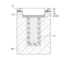
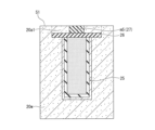
- FIG. 14A is a vertical cross-sectional view showing a cross-sectional configuration of the electrode 70, the charge accumulation region FD, and the insulating region 26 in a plane along a cutting line that crosses the body 71.
- FIG. 14A is a vertical cross-sectional view showing a cross-sectional configuration of the electrode 70 in a plane along a cutting line that crosses the first extension portion 71x of the body 71 shown in FIG. 14B as an example.
- the charge storage region FD is configured in a region of the cell region 20a consisting only of the first semiconductor region 20a1. More specifically, the charge storage region FD is configured in a region consisting only of the first semiconductor region 20a1 out of the first semiconductor region 20a1 and the second semiconductor region 20a2, and is not configured in the second semiconductor region 20a2. In addition, in a planar view, the entire charge storage region FD overlaps with the insulating region 26, and the surface of the charge storage region FD on the second surface S2 side is in contact with the insulating region 26. That is, the area occupied by the charge storage region FD in this embodiment is smaller than the area occupied by the charge storage region FD in the first embodiment.
- the impurity concentration of the charge storage region FD in this embodiment is set higher than the impurity concentration of the charge storage region FD in the first embodiment. Even if the area occupied by the charge storage region FD becomes smaller, the impurity concentration can be increased to suppress deterioration of the performance of accumulating charges. Furthermore, even if the area occupied by the charge storage region FD becomes smaller, and thus the contact area between the charge storage region FD and the electrode 70 decreases, the increase in contact resistance can be suppressed by increasing the impurity concentration.
- the charge storage region FD is configured in a region consisting only of the first semiconductor region 20a1. Therefore, in the vertical cross-sectional view of FIG. 14A, the relationship between dimension a, which is the horizontal dimension of the insulating region 26, distance b, which is the distance between the two charge storage regions FD facing each other via the body 71, and dimension d, which is the horizontal dimension of the charge storage region FD, can be expressed as a ⁇ 2d + b.
- the value obtained by adding the value of distance b to twice the value of dimension d is the same as or smaller than dimension a.
- 2d + b is the width occupied in the horizontal direction by the two charge storage regions FD facing each other via the body 71.
- head 72 overlaps the entire charge storage region FD. That is, the relationship between the above-mentioned distance b and dimension d, and dimension c, which is the dimension along the horizontal direction of head 72, can be expressed as c ⁇ 2d + b. In other words, dimension c is equal to or greater than the value obtained by adding the value of distance b to twice the value of dimension d. Furthermore, if the value of dimension c is fixed, distance b and dimension d can be determined so as to satisfy the above formula.
- the lower limit of dimension c is not limited to this, but may be, for example, the same width as the trench isolation wall 25.
- the lower limit of dimension d is not limited to this, but may be, for example, in the range of 1/4 to 1/5 of dimension c.
- 5E is the same as the manufacturing method according to the first embodiment described above. After that, as shown in FIG. 15A, a resist pattern R5 having an opening R5a is formed on the exposed surface. Then, using the resist pattern R5 as a mask for ion implantation, a known impurity that makes the semiconductor n-type is implanted from the first surface S1 side. The resist constituting the resist pattern R5 covers a part of the first semiconductor region 20a1 obtained by epitaxial growth. Then, another part of the first semiconductor region 20a1 is exposed from the opening R5a. By ion implanting the impurity through such an opening R5a, the charge storage region FD can be provided in a narrower region than in the first embodiment.
- the entire opening R5a overlaps with the insulating region 26 in a plan view. That is, the impurity is implanted into the semiconductor region that overlaps with the surface of the insulating region 26 on the first surface S1 side in a plan view. Therefore, even if the dose of the impurity is increased to increase the impurity concentration in the charge storage region FD, the progress of the impurity is blocked by the insulating region 26, making it difficult for the impurity to reach a deeper position. This allows the impurity to be confined at a high concentration in the region where the charge storage region FD is to be formed, and a fine charge storage region FD with a high impurity concentration can be formed.
- an insulating film m5 is formed on the exposed surface so as to fill the gaps between the charge storage regions FD. Then, the excess portions of the insulating film m5 are removed by CMP, and then the insulating film m2 is removed, obtaining the state shown in FIG. 15C. Then, as shown in FIG. 15D, the insulating film m1 and the excess portions of the insulating film m5 are removed by etch-back. A portion of the insulating film m5 remains between the charge storage regions FD, and hereinafter, this remaining insulating film m5 and the insulating region 26 are collectively referred to as the insulating region 26. Next, as shown in FIG. 15E, an electrode 70 is formed so as to contact the charge storage region FD. The subsequent processing is the same as that described in the first embodiment, and will not be described.
- the light detection device 1 according to the second embodiment of the present technology provides the same effects as the light detection device 1 according to the first embodiment described above.
- the charge storage region FD is configured as a region consisting of only the first semiconductor region 20a1 in the cell region 20a, and the entire charge storage region FD overlaps the insulating region 26 in a plan view.
- This allows the formation of a fine charge storage region FD with a high impurity concentration. Therefore, in the photodetector 1 according to the second embodiment of the present technology, as shown in FIG. 17, the distance between the charge storage region FD and the first portion G1a can be increased compared to the comparative example. This makes it possible to suppress the increase in the electric field strength between the charge storage region FD and the first portion G1a, and to suppress the deterioration of FD white spots.
- a charge storage region FD with a high impurity concentration can be formed, the deterioration of the charge storage performance can be suppressed even if the area occupied by the charge storage region FD becomes smaller, and the increase in the contact resistance between the charge storage region FD and the electrode 70 can be suppressed even if the contact area between the two is reduced.
- the horizontal dimension of the head 72 is c, and the horizontal dimension of the charge accumulation region FD is d, the relationship c ⁇ 2d+b is satisfied. That is, in a plan view, the head 72 overlaps the entire charge accumulation region FD, so that even if the area occupied by the charge accumulation region FD is reduced, the head 72 of the electrode 70 can be effectively brought into contact with the charge accumulation region FD.
- the impurity concentration of the charge accumulation region FD in this embodiment is higher, so that the contact resistance can be reduced compared to the first embodiment. Also, even if the contact area between the charge accumulation region FD and the electrode 70 is smaller than that in the first embodiment, the impurity concentration of the charge accumulation region FD in this embodiment is higher, so that the contact resistance can be suppressed from increasing.
- the width occupied in the horizontal direction by the two charge accumulation regions FD facing each other via the body portion 71 in a vertical cross section is equal to or less than the dimension in the horizontal direction of the insulating region 26 in the same cross section. In this way, even when one electrode 70 is provided for multiple charge accumulation regions FD, it is possible to form fine charge accumulation regions FD with a high impurity concentration.
- the photodetector 1 according to the first modification of the second embodiment shown in FIG. 18A is a combination of the first modification of the first embodiment and the second embodiment. More specifically, as shown in FIG. 18A, the first semiconductor region 20a1 is provided only at the corners of the cell region 20a, and the charge storage region FD of the second embodiment is provided for such a first semiconductor region 20a1. In this modification, the relationship between the dimension a, the distance b, the dimension c, and the dimension d is the same. In addition, the positional relationship and the size relationship between the electrode 70, the charge storage region FD, and the first semiconductor region 20a1 may be the relationship shown in FIG. 18B. Even with the photodetector 1 according to the first modification of the second embodiment, the same effect as that of the photodetector 1 according to the second embodiment described above can be obtained.
- the photodetector 1 according to the second modification of the second embodiment differs from the second embodiment in the manufacturing method.
- the manufacturing method of the photodetector 1 according to this modification will be described with reference to Figs. 19A and 19B. Note that in this modification, only the parts that differ from the manufacturing methods according to the first and second embodiments will be described. In the following description, the drawings used in the description of the manufacturing method according to the first embodiment will also be referred to as appropriate.
- first semiconductor region 20a1 is, for example, an intrinsic semiconductor (i-type), but may be p-type or n-type depending on the design, although this is not limited thereto.
- the conductivity type of first semiconductor region 20a1 may be formed to be the same conductivity type as second semiconductor region 20a2 or semiconductor region 21 depending on the design, or may be formed to be a different conductivity type.
- silicon is further epitaxially grown to obtain the remaining portion of the first semiconductor region 20a1.
- the silicon is epitaxially grown while injecting a known impurity that makes the semiconductor n-type.
- This makes it possible to form an n-type first semiconductor region 20a1, and the formed n-type region can be used as the charge accumulation region FD.
- the manufacturing method is the same as in the second embodiment, so a description will be omitted. Even with the photodetector 1 according to the second variation of the second embodiment, the same effects as those of the photodetector 1 according to the second embodiment described above can be obtained.
- the insulating region 26 has a flat shape in vertical cross section, which is the same as the insulating region 26 according to the first embodiment shown in Fig. 4F etc. Even in the photodetector 1 according to the third modification of the second embodiment, the same effects as those of the photodetector 1 according to the second embodiment described above can be obtained.
- the third embodiment of the present technology shown in Fig. 20A to Fig. 20D will be described below.
- the photodetector 1 according to the third embodiment includes a phase difference detector 80.
- the other configuration of the photodetector 1 is basically the same as that of the photodetector 1 of the first embodiment described above.
- the components already described are given the same reference numerals and their description will be omitted.
- Fig. 20A is a vertical cross-sectional view showing the cross-sectional configuration when viewed in cross section along the F-F cutting line in Fig. 20B
- Fig. 20C is a vertical cross-sectional view showing the cross-sectional configuration when viewed in cross section along the G-G cutting line in Fig. 20B
- Fig. 20B is an explanatory diagram showing the positional relationship of each component on the first surface S1.
- the first semiconductor region 20a1 and the second semiconductor region 20a2 are depicted separately.
- the semiconductor conductivity types such as the first conductivity type (e.g., p-type), the second conductivity type (e.g., n-type), and the i-type, are depicted without distinction.
- the first semiconductor layer 20 is mainly depicted, and other semiconductor layers and wiring layers may be omitted.
- only a part of the photodetector 1 is depicted, and some parts are omitted.
- the electrodes and wirings, such as the electrode 70, that are provided in contact with the first semiconductor region 20a1 are omitted.
- the trench isolation wall 25 of this embodiment is configured to include polysilicon 25b and an insulating film 25a, as in the first embodiment, but the insulating film 25a is omitted in the drawings according to this embodiment.
- the phase difference detection unit 80 includes a plurality of adjacent cell regions 20a (two in this embodiment). In order to distinguish the cell region 20a on the right side of the paper from the cell region 20a on the left side of the paper, the cell region on the right side of the paper is called cell region 20aR, and the cell region on the left side of the paper is called cell region 20aL. When there is no distinction between the two, they are simply called cell regions 20a.
- the photodetector 1 uses the phase difference detection unit 80 to determine the direction from which the light is incident.
- the photodetector 1 compares the amount of signal charge accumulated in the cell region 20aR with the amount of signal charge accumulated in the cell region 20aL to determine the direction from which the light is incident. For example, if the amount of signal charge accumulated in the cell region 20aR is greater than the amount of signal charge accumulated in the cell region 20aL, it is found that the light is incident on the photodetector 1 obliquely from the left side of the paper.
- the phase difference detection unit 80 also has a path PH through which signal charges can move between the cell region 20aR and the cell region 20aL.
- the path PH may be called an overflow path.
- the phase difference detection unit 80 can also function as one pixel 3.
- the phase difference detection unit 80 When the phase difference detection unit 80 also functions as a pixel 3, it outputs an addition signal, which is the sum of the amount of signal charges accumulated in the cell region 20aR and the amount of signal charges accumulated in the cell region 20aL, as a pixel signal. Therefore, when the signal charges are saturated first in one cell region, the signal charges overflow to the other cell region, and a part of the signal charges are prevented from being wasted. This prevents the linearity between the amount of light and the addition signal from deteriorating.
- the portion of the trench isolation wall 25 located between the two cell regions 20a (cell region 20aR, cell region 20aL) in the phase difference detection unit 80 is called the first trench isolation wall 25c to distinguish it from the other portions.
- the first trench isolation wall 25c is not distinguished from the other trench isolation walls 25, it is simply called the trench isolation wall 25.
- the first semiconductor region 20a1 is provided at a position overlapping the first trench isolation wall 25c in a plan view, and connects the cell region 20aR and the cell region 20aL in the phase difference detection unit 80.
- the first semiconductor region 20a1 included in the cell region 20aR and the first semiconductor region 20a1 included in the cell region 20aL are connected to each other at a position overlapping the first trench isolation wall 25c in a plan view to form one.
- the path PH is formed in the first semiconductor region 20a1 that is provided at a position that overlaps the first trench isolation wall 25c in a plan view.
- the conductivity type of the first semiconductor region 20a1 in which the path PH is formed may be any conductivity type that corresponds to the design.
- the end of the first trench isolation wall 25c on the first surface S1 side is recessed in the thickness direction from the other parts, and the insulating region 26 and the first semiconductor region 20a1 are provided only in the recessed portion 25d of the end of the first trench isolation wall 25c.
- FIG. 20D shows four phase difference detection units 80 arranged in two rows and two columns.
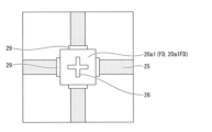
- the first semiconductor region 20a1 in which the charge storage region FD is configured is provided at the mutually opposing corners of the four phase difference detection units 80. Note that in this embodiment, the electrodes 70 are not shown.
- the first semiconductor region 20a1 in which the charge storage region FD is configured is a square ring shape in a plan view, and connects the mutually opposing corners of the four cell regions 20a at the corners of the phase difference detection unit 80.
- the first semiconductor region 20a1 in which the path PH is configured may be called the first semiconductor region 20a1PH
- the first semiconductor region 20a1 in which the charge storage region FD is configured may be called the first semiconductor region 20a1FD.
- the first semiconductor region 20a1FD is also provided in the recessed portion 25d of the trench isolation wall 25, similar to the first semiconductor region 20a1PH.
- the photodetector 1 may also have a contact region 24 having a similar configuration to the charge storage region FD, and the charge storage region FD may be read as the contact region 24 in the above description.
- the electrode 70 is provided for the first semiconductor region 20a1FD, the body 71 of the electrode 70 may be made columnar so as to fill the hollow portion of the ring-shaped first semiconductor region 20a1FD.
- the manufacturing method according to the first embodiment is the same as the manufacturing method according to the first embodiment described above up to the process shown in FIG. 5A.
- a trench STI is formed from the first surface S1 side so as to overlap the trench isolation wall 25 in a plan view by using known lithography and etching techniques.
- a resist pattern R3 may be formed first, and the insulating films m1, m2, and m3 may be etched using the resist pattern R3 as a mask, and the trench STI may be formed using the insulating films as a hard mask.
- the trench STI is formed in a lattice shape in a plan view, but in this embodiment, the trench STI is formed only in a square region using a resist pattern R3 having an opening R3a1 and an opening R3a2.
- the opening R3a1 of the resist pattern R3 is provided at a position where the first semiconductor region 20a1PH is formed in a plan view
- the opening R3a2 is provided at a position where the first semiconductor region 20a1FD is formed in a plan view.
- FIG. 5C shows an insulating film m4 so as to fill the inside of the trench STI, and as shown in FIG. 5D, an etchback is performed on the entire surface to remove unnecessary parts of the insulating film m4. Then, the insulating film m4 remaining at the bottom of the trench STI constitutes the insulating region 26.
- FIG. 22 shows the shape and position of the insulating region 26 in a plan view. Then, silicon is epitaxially grown on the surface 20c shown in FIG. 5D and FIG. 22 to obtain the first semiconductor region 20a1 shown in FIG. 23. Note that the surface 20c is a semiconductor surface exposed on the side wall of the trench STI.
- the epitaxial growth is controlled so that the first semiconductor regions 20a1 grown on the opposing surfaces 20c are not connected to each other, but in this embodiment, as shown in FIG. 23, the first semiconductor regions 20a1 grown on the opposing surfaces 20c are controlled to be connected to each other.
- cell region 20aR and cell region 20aL are electrically connected by first semiconductor region 20a1PH, and first semiconductor region 20a1FD becomes annular.
- the epitaxially grown first semiconductor region 20a1 is, for example, a true semiconductor (i-type), but may be p-type or n-type depending on the design, although it is not limited thereto. Furthermore, the conductivity type of the first semiconductor region 20a1 may be formed to be the same conductivity type as the second semiconductor region 20a2 or the semiconductor region 21 depending on the design, or may be formed to be a different conductivity type.
- the subsequent processing is the same as the processing described in the first embodiment and the known method for manufacturing the phase difference detection unit 80, and therefore a description thereof will be omitted.
- the path PH which is an overflow path in the thickness direction, may be provided at a position closer to the color filter 62. Therefore, the height of the first trench separation wall 25c that overlaps with the path PH in a plan view needs to be formed to a height different from the height of the other trench separation walls 25e, and stable height control may not be easy. In addition, there is a possibility that the signal charge generated in one of the cell regions 20aR and 20aL moves to the other cell region, deteriorating the isolation characteristics.
- the incident light L passes through the microlens 64 and the color filter 62, which have a low refractive index, and then passes through the path PH, which is made of a semiconductor with a high refractive index, and then enters the first trench isolation wall 25c, which has a low refractive index.
- the incident light L travels through the low refractive index region, the high refractive index region, and the low refractive index region, and there is a possibility that light reflection or scattering occurs when the incident light L enters the first trench isolation wall 25c, which has a low refractive index, from the path PH of the high refractive index region.
- the path PH is configured in the first semiconductor region 20a1PH provided on the surface opposite to the surface on the first trench isolation wall 25c side of the insulating region 26.
- the path PH can be provided at a position closer to the first surface S1 rather than a position closer to the second surface S2. Therefore, in the thickness direction, the position of the end of the first trench isolation wall 25c on the color filter 62 side can be aligned with the position of the end of the other trench isolation wall 25 on the color filter 62 side, and the deterioration of the isolation characteristics can be suppressed.
- the position of the end of the first trench isolation wall 25c on the color filter 62 side can be aligned with the position of the end of the other trench isolation walls 25 on the color filter 62 side, so that when forming the first trench isolation wall 25c and the other trench isolation walls 25 from the first surface S1 side, all of the trench isolation walls can be formed to the same depth, which prevents the manufacturing load from becoming too large.
- the photodetector 1 also has an insulating region 26 made of an insulating material and provided between the end of the first trench isolation wall 25c closer to the first surface S1 and the first semiconductor region 20a1PH. Since the insulating region 26 is interposed between the first trench isolation wall 25c and the first semiconductor region 20a1PH, when the trench isolation wall 25 has a portion made of a conductor such as polysilicon, the conductive portion of the trench isolation wall 25 can be electrically insulated from the path PH. In addition, the flow of signal charges in the path PH can be concentrated mainly in the horizontal direction. Furthermore, by providing the insulating region 26, the difference in impurity concentration between the first semiconductor region 20a1 and other semiconductor regions such as the photoelectric conversion unit 22 can be made clear.
- the charge storage region FD and the contact region 24 can be configured in a region including at least a portion of the first semiconductor region 20a1.
- the insulating region 26 may be arranged in a lattice shape in a plan view, as shown in FIG. 4C according to the first embodiment.
- an insulating isolation region 29 made of an insulating material is provided between the sidewall 25f of the recessed portion 25d of the first trench isolation wall 25c and the first semiconductor region 20a1PH. Also, an insulating isolation region 29 made of an insulating material is provided between the sidewall 25f of the recessed portion 25d of the trench isolation wall 25 and the first semiconductor region 20a1FD.
- the material constituting the insulating isolation region 29 is a known insulating material.
- the insulating isolation region 29 may be made of the same material as the material constituting the insulating region 26.
- the manufacturing method according to this modified example is the same as the manufacturing method according to the third embodiment up to the step of depositing insulating film m4 so as to fill the inside of the STI trench, as shown in FIG. 5C. Thereafter, although not shown in the figure, the excess portion of insulating film m4 and insulating film m3 are removed by, for example, a CMP method. This exposes insulating film m2.
- a resist pattern R4 having openings R4a1 and R4a2 is formed by a known lithography technique.
- the opening R4a1 is provided at a position where the first semiconductor region 20a1PH is formed in a plan view
- the opening R4a2 is provided at a position where the first semiconductor region 20a1FD is formed in a plan view.
- the portions exposed from the openings R4a1 and R4a2 are etched back to remove unnecessary portions of the insulating film m4, thereby obtaining an insulating region 26.
- the shapes of the openings R4a1 and R4a2 are compared with the shapes of the openings R3a1 and R3a2 of the resist pattern R3 shown in FIG. 21.
- the size of the openings R3a1 and R3a2 is the same as the size of the recessed portion 25d of the trench isolation wall 25.
- the dimension of the opening R4a1 in the direction along the extension direction (Y direction) of the first trench isolation wall 25c is smaller than that of the opening R3a1. Therefore, both ends of the insulating film m4 embedded in the recessed portion 25d along the Y direction are covered with resist and remain without being etched back. This allows an insulating isolation region 29 to be provided between the first semiconductor region 20a1 and the sidewall 25f of the recessed portion 25d of the first trench isolation wall 25c.
- the dimension of the opening R4a1 along the width direction (X direction) of the first trench isolation wall 25c is larger than that of the opening R3a1, and the insulating film m2 and the insulating film m4 are exposed in the opening R4a1.
- the etch-back due to the difference in etching rate between the insulating film m2 and the insulating film m4, even if the insulating film m2 is etched, it is only slightly.
- the opening R4a2 is provided at a position where the trench isolation wall 25 intersects in a plan view. Therefore, the shape and dimensions of the opening R4a2 are determined so that the insulating film m4 remains at the ends in both the X and Y directions. Also, since it is necessary to epitaxially grow silicon on the semiconductor surface, the opening R4a2 is widened so that the insulating film m4 does not remain on the surface 20c. More specifically, the dimensions in the X and Y directions at the corners of the opening R4a2 are made larger than those of the opening R3a2, and between the corners, at least in the region wider than the trench isolation wall 25, the dimensions in the X and Y directions are made smaller than those of the opening R3a2. This allows an insulating isolation region 29 to be provided between the first semiconductor region 20a1 and the sidewall 25f of the recessed portion 25d of the first trench isolation wall 25c.
- an insulating isolation region 29 made of an insulating material is provided between the sidewall 25f of the recessed portion 25d of the trench isolation wall 25 and the first semiconductor region 20a1. Therefore, silicon can be epitaxially grown in a state where the polysilicon material of the trench isolation wall 25 is covered with the insulating isolation region 29, and silicon can be grown only on the surface 20c out of the sidewall 25f and the surface 20c. This makes it possible to suppress abnormal growth of silicon crystals on the sidewall 25f of the trench isolation wall 25.
- the first semiconductor region 20a1FD in which the charge storage region FD is formed is not annular, but is composed of four portions provided for each cell region 20a, as in the first embodiment. Note that the first semiconductor region 20a1FD may be provided with a contact region 24 instead of the charge storage region FD.
- the dimensions of the opening R3a2 in the X direction and the Y direction of the opening R3a2 in the resist pattern R3 shown in FIG. 21 may be made larger than the dimension of the opening R3a1 in the X direction (width direction of the trench isolation wall 25). This allows the time required for the first semiconductor regions 20a1 grown on the opposing surfaces 20c to be connected to each other to be longer at the position where the first semiconductor region 20a1FD is provided than at the position where the first semiconductor region 20a1PH is provided. As a result, when the first semiconductor region 20a1PH is obtained, the first semiconductor region 20a1FD is still not connected, and the first semiconductor region 20a1FD shown in FIG. 27 is obtained.
- the light detection device 1 according to the modified example 2 of the third embodiment can be provided with an electrode 70 having a shape similar to that of the first embodiment.
- the first semiconductor region 20a1FD in which the charge accumulation region FD is formed may be connected in a ring shape, and a cross-shaped gap may be provided in the center.
- the same effects as the light detection device 1 according to the third embodiment described above can be obtained. Furthermore, the light detection device 1 according to modified example 3 of the third embodiment can be provided with an electrode 70 having a shape similar to that of the first embodiment.
- the trench isolation wall 25 includes the polysilicon 25b and the insulating film 25a, but the present technology is not limited to this.
- the trench isolation wall 25 of the photodetector 1 according to the fourth modification of the third embodiment may be formed only of a known insulating film such as silicon oxide.
- the trench isolation wall 25 is made of only silicon oxide having a lower refractive index than the path PH, and its end faces the second surface S2 side, and the high refractive index path PH is not provided on the color filter 62 side. Therefore, when considering light passing through the microlens 64, the color filter 62, and the trench isolation wall 25 in that order, the light passes through the microlens 64 and the color filter 62, which have a lower refractive index than the path PH, and then directly enters the trench isolation wall 25 without passing through a high refractive index region. As a result, the light enters the low refractive index region from the low refractive index region, and reflection and scattering of the light when it enters the trench isolation wall 25 can be suppressed.
- the electronic device 100 includes a solid-state imaging device 101, an optical lens 102, a shutter device 103, a driving circuit 104, and a signal processing circuit 105.
- the electronic device 100 is, but is not limited to, an electronic device such as a camera.
- the electronic device 100 also includes the above-mentioned photodetector 1 as the solid-state imaging device 101.
- the optical lens (optical system) 102 focuses image light (incident light 106) from the subject onto the imaging surface of the solid-state imaging device 101. This causes signal charges to accumulate in the solid-state imaging device 101 for a certain period of time.
- the shutter device 103 controls the light irradiation period and light blocking period for the solid-state imaging device 101.
- the drive circuit 104 supplies a drive signal that controls the transfer operation of the solid-state imaging device 101 and the shutter operation of the shutter device 103.
- the drive signal (timing signal) supplied from the drive circuit 104 transfers signals from the solid-state imaging device 101.
- the signal processing circuit 105 performs various signal processing on signals (pixel signals) output from the solid-state imaging device 101.
- the video signals that have undergone signal processing are stored in a storage medium such as a memory, or output to a monitor.
- the electronic device 100 includes a first semiconductor region 20a1 provided on the surface of the insulating region 26 opposite the surface on the trench isolation wall 25 side in the solid-state imaging device 101, thereby improving the image quality of the video signal.
- the electronic device 100 is not limited to a camera, but may be other electronic devices.
- it may be an imaging device such as a camera module for a mobile device such as a mobile phone.
- the electronic device 100 may also include, as the solid-state imaging device 101, a photodetector 1 according to any one of the first to third embodiments and modified versions of those embodiments, or a photodetector 1 according to a combination of at least two of the first to third embodiments and modified versions of those embodiments.
- the photodetector 1 according to variant 6 of the first embodiment described above has only two semiconductor layers, but such a technical idea can be applied to the photodetector 1 described in the second and third embodiments.
- the photodetector 1 according to the third embodiment described above has a phase difference detection section 80, but such a technical idea can be applied to the photodetector 1 described in the first and second embodiments, and various combinations according to the respective technical ideas are possible.
- this technology can be applied to light detection devices in general, including not only the solid-state imaging devices as image sensors described above, but also distance measurement sensors that measure distance, also known as ToF (Time of Flight) sensors.
- Distance measurement sensors emit light toward an object, detect the light that is reflected back from the surface of the object, and calculate the distance to the object based on the flight time from when the light is emitted to when the reflected light is received.
- the structure of the pixel 3 described above can be adopted as the structure of this distance measurement sensor.
- the materials listed as constituting the above-mentioned components may contain additives, impurities, etc.
- the present technology may be configured as follows. (1) a first semiconductor layer having a plurality of cell regions arranged in a matrix along row and column directions in a plan view, the first semiconductor layer having one surface on which an element is formed and the other surface on which a light is incident; a trench isolation wall separating the cell regions; an insulating region that is provided at an end of the trench isolation wall close to the element formation surface, has a dimension along a width direction larger than a dimension along the width direction of the trench isolation wall in a plan view, and is made of an insulating material; A photoelectric conversion unit is configured in the cell region, the cell region includes a first semiconductor region provided on a surface of the insulating region opposite to a surface on the trench isolation wall side; Light detection device.
- An optical detection device as described in (1).
- the charge storage regions are provided at mutually opposing corners of the cell regions in a plan view
- the body portion has a first extending portion extending along the row direction and the thickness direction, and a second extending portion extending along the column direction and the thickness direction and intersecting the first extending portion in a plan view;
- the photodetector according to any one of (4) to (6), wherein the charge accumulation region is in contact with the body portion at a recessed corner formed by the first extension portion and the second extension portion.
- a contact electrode having a contact body and a contact head having one surface connected to one end of the contact body, a contact region fixed to a reference potential via the contact electrode is formed in a region of the cell region including at least a part of the first semiconductor region, the other end of the contact body is in contact with a surface of the insulating region closer to the element forming surface, the contact electrode is in contact with the contact region via a side surface of the contact body and one surface of the contact head.
- An optical detection device according to any one of (2) to (7).
- a phase difference detection unit having two adjacent cell regions and a path through which a signal charge can move between the two adjacent cell regions;
- the first semiconductor region is provided at a position overlapping the first trench isolation wall in a plan view and connects the two cell regions in the phase difference detection unit, The path is configured in the first semiconductor region.
- An optical detection device as described in (1).
- a portion of an end portion of the first trench isolation wall on the element formation surface side is recessed in a thickness direction from other portions, The photodetector according to (15), wherein the insulating region and the first semiconductor region are provided only in a recessed portion of the end portion.
- a light detection device and an optical system that forms an image of light from a subject on the light detection device includes: a first semiconductor layer having a plurality of cell regions arranged in a matrix along row and column directions in a plan view, the first semiconductor layer having one surface on which an element is formed and the other surface on which a light is incident; a trench isolation wall separating the cell regions; an insulating region that is provided at an end of the trench isolation wall close to the element formation surface, the insulating region having a dimension along a width direction larger than a dimension along the width direction of the trench isolation wall in a plan view, and that is made of an insulating material;
- a photoelectric conversion unit is configured in the cell region, the cell region includes a first semiconductor region provided on a surface of the insulating region opposite to a surface of
- Photodetector 20 First semiconductor layer 20a, 20aL, 20aR Cell region 20a1, 20a1FD, 20a1PH First semiconductor region 20b Isolation region 24 Contact region (semiconductor region) 25 Trench isolation wall 25c First trench isolation wall 25d Recessed portion 25f Side wall 26 Insulating region 29 Insulating isolation region 70 Electrode 70 Contact electrode 71 Body 71 Contact body 71x First extension portion 71y Second extension portion 72 Head 72 Contact head 80 Phase difference detection portion 100 Electronic device 102 Optical system a Dimension b Distance c Dimension d Dimension FD Charge storage region PH Path W1, W2 Dimensions
Landscapes
- Solid State Image Pick-Up Elements (AREA)
- Element Separation (AREA)
Abstract
Description
1.第1実施形態
2.第2実施形態
3.第3実施形態
4.第4実施形態
電子機器への応用例
この実施形態では、裏面照射型のCMOS(Complementary Metal Oxide Semiconductor)イメージセンサである光検出装置に本技術を適用した一例について説明する。
まず、光検出装置1の全体構成について説明する。図1に示すように、本技術の第1実施形態に係る光検出装置1は、平面視したときの二次元平面形状が方形状の半導体チップ2を主体に構成されている。すなわち、光検出装置1は、半導体チップ2に搭載されている。この光検出装置1は、図29に示すように、光学系(光学レンズ)102を介して被写体からの像光(入射光106)を取り込み、撮像面上に結像された入射光106の光量を画素単位で電気信号に変換して画素信号として出力する。
図2に示すように、半導体チップ2は、ロジック回路13を備えている。ロジック回路13は、垂直駆動回路4、カラム信号処理回路5、水平駆動回路6、出力回路7及び制御回路8などを含んでいる。ロジック回路13は、電界効果トランジスタとして、例えば、nチャネル導電型のMOSFET(Metal Oxide Semiconductor Field Effect Transistor)及びpチャネル導電型のMOSFETを有するCMOS(Complenentary MOS)回路で構成されている。
図3は、画素3の一構成例を示す等価回路図である。図示の例では、複数の画素3が、1つの読出し回路15を共有している。より具体的には、4つの画素3が、1つの読出し回路15を共有している。画素3のそれぞれは、光電変換素子PDと、光電変換素子PDで光電変換された信号電荷を電荷蓄積領域FDに転送する転送トランジスタTRと、電荷蓄積領域(フローティングディフュージョン:Floating Diffusion)FDと、を備えている。読出し回路15は、電荷蓄積領域FDの後段に接続されている。
次に、光検出装置1の具体的な構成について、図4Aから図4Hまでを用いて説明する。なお、図面によっては、バリアメタル層及びトランジスタのゲート絶縁膜の記載を省略している場合がある。
図4Aは、図4B及び図4C等のA-A切断線に沿って断面視した時の断面構成を示す横断面図である。図4Aに示すように、光検出装置1(半導体チップ2)は、例えば、一方の面が第1の面S1であり他方の面が第2の面S2である第1半導体層20と、第1配線層30と、第2半導体層40と、第2配線層50と、図示を省略した第3半導体層と、をその順で積層した積層構造を有する。また、光検出装置1(半導体チップ2)は、第2の面S2側に光入射面側積層体60を有する。
第1半導体層20は、半導体基板で構成されている。第1半導体層20は、これには限定されないが、例えば、主に単結晶シリコン(Si)基板で構成されている。なお、第1の面S1を素子形成面又は主面と呼び、第2の面S2を光入射面又は裏面と呼ぶこともある。第1半導体層20の画素領域2Aに相当する部分には、平面視で行方向及び列方向に沿ってマトリクス状に配列された複数のセル領域20aが設けられている。セル領域20aは、画素3毎に設けられている。例えば、分離領域20bで区画された島状のセル領域20aが画素3毎に設けられている。なお、画素3の数は、図4Aに限定されるものではない。
図4Aに示すように、トレンチ分離壁25の第1の面S1寄りの端部には、絶縁材料からなる絶縁領域26が設けられている。絶縁領域26は、一方の面(第2の面S2寄りの面)がトレンチ分離壁25の第1の面S1寄りの端部に接している。図4Cは、図4AのC-C切断線に沿って断面視した時の断面構成を示す横断面図である。図4Cに示すように、絶縁領域26は、平面視で、セル領域20a同士の間を区画するように行方向及び列方向に沿って延在している。平面視で、絶縁領域26は、トレンチ分離壁25に沿って設けられ且つトレンチ分離壁25に重なっている。より具体的には、平面視で、トレンチ分離壁25の全体は、絶縁領域26に重なっている。また、絶縁領域26は、平面視でトレンチ分離壁25が設けられた場所全体に対して設けられている。絶縁領域26の幅方向に沿った寸法はW2であり、トレンチ分離壁25の幅方向に沿った寸法W1より大きい(W2>W1)。絶縁領域26を構成する絶縁材料は、これには限定されないが、酸化シリコン(SiO2)等の材料を挙げることができる。
図4F及び図4Gに示すように、第1半導体領域20a1は、厚み方向において、絶縁領域26と第1の面S1との間に設けられていて、一方の面が絶縁領域26の第1の面S1寄りの面に接し、他方の面が第1の面S1に臨んでいる。より具体的には、第1半導体領域20a1は、セル領域20aのうち、絶縁領域26の第1の面S1寄りの面に設けられた部分であり、且つ平面視で絶縁領域26と重なる部分である。
図4Aに示すように、光検出装置1は電極70を有している。電極70には、電荷蓄積領域FDに電気的に接続された電極70と、コンタクト領域24に電気的に接続された電極70とがあるが、両者の構成は同様なので、ここでは、電荷蓄積領域FDに電気的に接続された電極70を例として説明する。
図4A及び図4Eに示すように、転送トランジスタT1は、セル領域20a毎に設けられている。転送トランジスタT1は、光電変換部22内で生成された信号電荷を電荷蓄積領域FDに転送可能なトランジスタである。例えば、転送トランジスタT1がオンした場合に光電変換部22と電荷蓄積領域FDとの間が導通し、信号電荷が電荷蓄積領域FDに転送される。そして、転送トランジスタT1がオフした場合に光電変換部22と電荷蓄積領域FDとの間の導通が遮断される。
図4Aに示すように、第1配線層30は、一方の面が第1半導体層20に接し、他方の面が第2配線層50に接した多層配線層である。第1配線層30は、これには限定されないが、例えば、絶縁膜31と、絶縁膜31内に設けられた配線32を有する。配線32は、主に厚み方向に延在する縦配線と、主に水平方向に延在する横配線とを含む。絶縁膜31は、例えば酸化シリコン(SiO2)膜、窒化シリコン(Si3N4)膜、酸窒化シリコン(SiON)膜等の公知の絶縁膜を複数層積層した構成である。配線32は、例えばポリシリコン等の半導体材料、銅(Cu)、タングステン(W)、アルミニウム(Al)等の金属材料など、公知の導電性材料である。
第2半導体層40は、半導体基板で構成されている。第2半導体層40は、これには限定されないが、例えば、単結晶シリコン基板で構成されていて、一方の面が第1配線層30に接し、他方の面が第2配線層50に接している。第2半導体層40には、トランジスタT2が複数設けられている。トランジスタT2は、例えば、図3に示した読出し回路15を構成するトランジスタを含んでいる。
第2配線層50は、一方の面が第2半導体層40に接し、他方の面が図示を省略した第3半導体層に接した多層配線層である。第2配線層50は、これには限定されないが、例えば、複数層積層された絶縁膜51と、絶縁膜51内に設けられた配線52を有する。配線52は、主に厚み方向に延在する縦配線と、主に水平方向に延在する横配線とを含む。縦配線は、図4Aに示すように、第2半導体層を貫通する貫通配線を含んでいても良い。配線52は、主に厚み方向に延在する縦配線と、主に水平方向に延在する横配線とを含む。絶縁膜51は、例えば酸化シリコン(SiO2)膜、窒化シリコン(Si3N4)膜、酸窒化シリコン(SiON)膜等の公知の絶縁膜を複数層積層した構成である。配線52は、例えばポリシリコン等の半導体材料、銅(Cu)、タングステン(W)、アルミニウム(Al)等の金属材料など、公知の導電性材料である。
図示を省略する第3半導体層は、半導体基板で構成されている。第3半導体層は、これには限定されないが、例えば、単結晶シリコン基板で構成されていて、一方の面が第2配線層50に接している。第3半導体層には、例えば、図2に示したロジック回路13を構成するトランジスタが設けられている。
光入射面側積層体60は、これには限定されないが、例えば、平坦化膜61と、カラーフィルタ62、遮光壁63、マイクロレンズ(オンチップレンズ)64と、を第2の面S2側からその順で積層した積層構造を有する。平坦化膜61は、公知の絶縁材料又は公知の樹脂材料で構成されていて、これには限定されないが、例えば、酸化シリコンで構成されていても良い。カラーフィルタ62は、セル領域20aへの入射光を色分離する。遮光壁63は、カラーフィルタ62は、例えば樹脂性の材料で構成されている。カラーフィルタ62同士の間には、迷光を遮光する遮光壁63が設けられている。マイクロレンズ64は、例えば樹脂性の材料で構成されている。
以下、図5Aから図5Jまでを参照して、光検出装置1の製造方法について説明する。なお、本実施形態では、主に絶縁領域26と、電荷蓄積領域FDと、電極70との形成方法について説明し、それ以外の部分については説明を省略する。
以下、第1実施形態の主な効果を説明するが、その前に、図6に示す比較例に係る光検出装置について説明する。比較例においては、トレンチ分離壁25の第1の面S1寄りの端部には、絶縁膜が埋め込まれたシャロ―トレンチ26Aが設けられている。そして、4つの電荷蓄積領域FDは、シャロ―トレンチ26Aにより区画されている。電極70Aは、水平方向に延在する板状の部材のみからなり、第1半導体層20側の面を介して、4つの電荷蓄積領域FDに接触している。
以下、第1実施形態の変形例について、説明する。
第1実施形態に係る光検出装置1では、図4Dに示すように、第1半導体領域20a1は、第1の面S1において、セル領域20aの縁部全体に亘って設けられていたが、本技術はこれには限定されない。図7Aに示す第1実施形態の変形例1に係る光検出装置1では、第1半導体領域20a1は、第1の面S1において、セル領域20aの角部にのみ設けられている。角部以外の部分は、図7Bに示すように、第1半導体領域20a1が設けられていない。図7AのA-A切断線に沿った平面で光検出装置1を縦断面視した断面構成は、図4Fと同じである。図7Bは、図7AのE-E切断線に沿った平面で光検出装置1を縦断面視した断面構成を示す。図7Bに示すように、セル領域20aの角部以外の領域には、第1半導体領域20a1が設けられていない。図7Aに示すように、電荷蓄積領域FDは、セル領域20aの1つの角部に対して設けられた第1半導体領域20a1の全ての領域を含む半導体領域に構成されている。
図10に示す第1実施形態の変形例2に係る光検出装置1では、ゲート電極G1は、形状が方形であっても良く、平面視の面積が第1実施形態の場合より大きくても良い。また、平面視で、電極70の頭部72は、八角形ではなく方形であっても良い。また、図10に示す画素は、位相差を検出する位相差検出部であっても良い。なお、図10では、電荷蓄積領域FDの図示を省略している。この第1実施形態の変形例2に係る光検出装置1であっても、上述の第1実施形態に係る光検出装置1と同様の効果が得られる。
図11に示す第1実施形態の変形例3に係る光検出装置1は、上述の変形例1と変形例2との組み合わせである。より具体的には、図11に示すように、第1半導体領域20a1はセル領域20aの角部のみに設けられていて、ゲート電極G1及び頭部72は上述の変形例2と同じである。なお、図11では、電荷蓄積領域FDの図示を省略している。この第1実施形態の変形例3に係る光検出装置1であっても、上述の第1実施形態に係る光検出装置1と同様の効果が得られる。
図12に示す第1実施形態の変形例4に係る光検出装置1では、電極70の頭部72は平面視で楕円形であり、第1半導体領域20a1はセル領域20aの角部のみに設けられている。なお、図12では、電荷蓄積領域FDの図示を省略している。この第1実施形態の変形例4に係る光検出装置1であっても、上述の第1実施形態に係る光検出装置1と同様の効果が得られる。
図13に示す第1実施形態の変形例5に係る光検出装置1では、電極70の頭部72は平面視で円形であり、第1半導体領域20a1はセル領域20aの角部のみに設けられている。なお、図13では、電荷蓄積領域FDの図示を省略している。この第1実施形態の変形例5に係る光検出装置1であっても、上述の第1実施形態に係る光検出装置1と同様の効果が得られる。
第1実施形態及びその変形例では、光検出装置1(半導体チップ2)は、例えば、第1半導体層20と、第2半導体層40と、図示を省略した第3半導体層との三層の半導体層を有していたが、本技術はこれには限定されない。第1実施形態の変形例6に係る光検出装置1では、三層の半導体層のうちの第1半導体層20と第3半導体層との二層のみを有していても良い。その場合、第2半導体層40に構成された素子は、第1半導体層20等に構成されればよい。この第1実施形態の変形例6に係る光検出装置1であっても、上述の第1実施形態に係る光検出装置1と同様の効果が得られる。
図14A及び図14Bに示す本技術の第2実施形態について、以下に説明する。本第2実施形態に係る光検出装置1は、電荷蓄積領域FDが占める領域の大きさが異なる。それ以外の光検出装置1の構成は、基本的に上述の第1実施形態の光検出装置1と同様の構成になっている。すでに説明した構成要素については、同じ符号を付してその説明を省略する。なお、図14Aは、胴部71を横切る切断線に沿った平面で電極70と、電荷蓄積領域FDと、絶縁領域26と、を断面視した断面構成を示す縦断面図である。本実施形態では、図14Aは、一例として、図14Bに示す胴部71の第1延在部分71xを横切る切断線に沿った平面で電極70を断面視した断面構成を示す縦断面図である。
以下、図15Aから図15Eまでを参照して、光検出装置1の製造方法について説明する。なお、本変形例では、上述の第1実施形態に係る製造方法と異なる部分についてのみ、説明する。また、以下の説明では第1実施形態に係る製造方法の説明に用いた図面についても、適宜参照する。
以下、第2実施形態の主な効果を説明するが、その前に、図16に示す比較例に係る光検出装置について説明する。図16に示すように、平面視で、電荷蓄積領域FDとゲート電極G1が有する柱状の第1部分G1aとの間の距離が小さくなり過ぎると、電荷蓄積領域FDと第1部分G1aとの間の電界強度が大きくなってFD白点が悪化する可能性があった。しかし、電荷蓄積領域FDと第1部分G1aとの間の距離を広げるために電荷蓄積領域FD及び電極70Aを微細化すると、電荷蓄積領域FDと電極70Aとの接触面積が減少し、接触抵抗が高くなる可能性があった。これにより、電荷蓄積領域FDと電極70Aとの電気的接続が劣化する可能性があった。
以下、第2実施形態の変形例について、説明する。
図18Aに示す第2実施形態の変形例1に係る光検出装置1は、第1実施形態の変形例1と第2実施形態との組み合わせである。より具体的には、図18Aに示すように、第1半導体領域20a1は、セル領域20aの角部のみに設けられていて、そのような第1半導体領域20a1に対して、第2実施形態の電荷蓄積領域FDが設けられている。本変形例においても、寸法aと、距離bと、寸法cと、寸法dと、の関係は同じである。また、電極70と、電荷蓄積領域FDと、第1半導体領域20a1との位置関係及び大小関係は、図18Bに示す関係であっても良い。この第2実施形態の変形例1に係る光検出装置1であっても、上述の第2実施形態に係る光検出装置1と同様の効果が得られる。
第2実施形態の変形例2に係る光検出装置1は、製造方法において第2実施形態と異なる。以下、図19A及び図19Bを参照して、本変形例に係る光検出装置1の製造方法について説明する。なお、本変形例では、上述の第1実施形態及び第2実施形態に係る製造方法と異なる部分についてのみ、説明する。また、以下の説明では第1実施形態に係る製造方法の説明に用いた図面についても、適宜参照する。
第2実施形態の変形例3に係る光検出装置1は、縦断面視した場合の絶縁領域26の形状が平板状であり、図4F等に示す第1実施形態に係る絶縁領域26の形状と同じである。この第2実施形態の変形例3に係る光検出装置1であっても、上述の第2実施形態に係る光検出装置1と同様の効果が得られる。
図20Aから図20Dまでに示す本技術の第3実施形態について、以下に説明する。本第3実施形態に係る光検出装置1は、位相差検出部80を含む。それ以外の光検出装置1の構成は、基本的に上述の第1実施形態の光検出装置1と同様の構成になっている。すでに説明した構成要素については、同じ符号を付してその説明を省略する。なお、図20Aは図20BのF-F切断線に沿って断面視した時の断面構成を示す縦断面図であり、図20Cは図20BのG-G切断線に沿って断面視した時の断面構成を示す縦断面図であり、図20Bは、第1の面S1における各構成要素の位置関係を示す説明図である。
以下、図21から図23までを参照して、光検出装置1の製造方法について説明する。なお、本実施形態では、上述の第1実施形態に係る製造方法と異なる部分についてのみ、説明する。また、以下の説明で参照される縦断面図は、図20BのF-F切断線に沿った縦断面図の一部を示している。また、以下の説明では第1実施形態に係る製造方法の説明に用いた図面についても、適宜参照する。
以下、第3実施形態の主な効果を説明するが、その前に、画素3の微細化及び図24に示す比較例について説明する。位相差検出部80内の2つのセル領域20a同士の間に不純物分離構造を設けることにより、厚み方向において第1の面S1側にオーバーフローパスである経路PHを設けることができる。しかし、画素のさらなる微細化が望まれており、位相差検出部80をより微細化する場合には、2つのセル領域20a同士の間に不純物分離構造を設けることが容易ではなくなる可能性がある。その場合、図24の比較例に示すように、2つのセル領域20a同士の間を第1トレンチ分離壁25cで分離することが求められる。そして、厚み方向においてオーバーフローパスである経路PHをカラーフィルタ62寄りの位置に設ける可能性がある。そのため、平面視で経路PHに重なる第1トレンチ分離壁25cの高さを、他のトレンチ分離壁25eの高さと異なる高さに形成する必要があり、安定した高さ制御が容易ではない可能性がある。また、セル領域20aR及びセル領域20aLの一方のセル領域において生成された信号電荷が他方のセル領域に移動して、分離特性が劣化する可能性がある。また、第1トレンチ分離壁25cが酸化シリコンで形成されている場合、入射光Lは、屈折率が低いマイクロレンズ64及びカラーフィルタ62を通過した後、屈折率が高い半導体からなる経路PHを通過し、その後再び屈折率が低い第1トレンチ分離壁25cに入射する。その場合、入射光Lは、低屈折率領域、高屈折率領域、低屈折率領域に進み、特に高屈折率領域の経路PHから低屈折率の第1トレンチ分離壁25cに入射する際に光の反射や散乱が生じる可能性がある。
以下、第3実施形態の変形例について、説明する。
図25A及び図25Bに示す第3実施形態の変形例1に係る光検出装置1では、第1トレンチ分離壁25cの窪んだ部分25dの側壁25fと第1半導体領域20a1PHとの間には、絶縁材料からなる絶縁分離領域29が設けられている。また、トレンチ分離壁25の窪んだ部分25dの側壁25fと第1半導体領域20a1FDとの間には、絶縁材料からなる絶縁分離領域29が設けられている。絶縁分離領域29を構成する材料は、公知の絶縁材料である。絶縁分離領域29は、絶縁領域26を構成する材料と同じ材料により構成されていても良い。
図27に示す第3実施形態の変形例2に係る光検出装置1では、電荷蓄積領域FDが構成された第1半導体領域20a1FDが環状ではなく、第1実施形態の場合と同様に、セル領域20a毎に設けられた4つの部分からなる。なお、第1半導体領域20a1FDには、電荷蓄積領域FDの代わりにコンタクト領域24が設けられていても良い。
図28に示す第3実施形態の変形例3に係る光検出装置1では、電荷蓄積領域FDが構成された第1半導体領域20a1FDが環状につながっていて、且つ中央部に十字状に隙間があっても良い。
第3実施形態では、トレンチ分離壁25は、ポリシリコン25bと、絶縁膜25aとを含んで構成されていたが、本技術はこれには限定されない。第3実施形態の変形例4に係る光検出装置1が有するトレンチ分離壁25は、例えば酸化シリコンのような公知の絶縁膜のみにより構成されていても良い。
<1.電子機器への応用例>
次に、図29に示す本技術の第4実施形態に係る電子機器100について説明する。電子機器100は、固体撮像装置101と、光学レンズ102と、シャッタ装置103と、駆動回路104と、信号処理回路105とを備えている。電子機器100は、これに限定されないが、例えば、カメラ等の電子機器である。また、電子機器100は、固体撮像装置101として、上述の光検出装置1を備えている。
上記のように、本技術は第1実施形態から第4実施形態までによって記載したが、この開示の一部をなす論述及び図面は本技術を限定するものであると理解すべきではない。この開示から当業者には様々な代替の実施形態、実施例及び運用技術が明らかとなろう。
(1)
一方の面が素子形成面であり他方の面が光入射面であり、且つ平面視で行方向及び列方向に沿ってマトリクス状に配列された複数のセル領域を有した第1半導体層と、
前記セル領域同士の間を区画しているトレンチ分離壁と、
前記トレンチ分離壁の前記素子形成面寄りの端部に設けられ、平面視で、幅方向に沿った寸法が前記トレンチ分離壁の幅方向に沿った寸法より大きく、且つ絶縁材料からなる絶縁領域と、を備え、
前記セル領域には光電変換部が構成されていて、
前記セル領域は、前記絶縁領域の前記トレンチ分離壁側の面とは反対側の面に設けられた第1半導体領域を含む、
光検出装置。
(2)
胴部と前記胴部の一方の端部に一方の面が接続された頭部とを有した電極を備え、
前記セル領域のうち前記第1半導体領域の少なくとも一部を含む領域には、電荷蓄積領域が構成されていて、
前記胴部の他方の端部は、前記絶縁領域の前記素子形成面寄りの面に接し、
前記電極は、前記胴部の側面と前記頭部の一方の面とを介して、前記電荷蓄積領域に接している、
(1)に記載の光検出装置。
(3)
前記胴部の側面と前記頭部の一方の面とは、前記電荷蓄積領域が構成された前記第1半導体領域に接している、(2)に記載の光検出装置。
(4)
前記電極は、それぞれ異なる前記セル領域に設けられた複数の前記電荷蓄積領域に接している、(2)又は(3)に記載の光検出装置。
(5)
縦断面視において、前記胴部を介して対向する2つの前記電荷蓄積領域同士の間の距離をbとし、前記絶縁領域の水平方向に沿った寸法をaとした場合、b<aの関係を満たす、(4)に記載の光検出装置。
(6)
前記縦断面視において、前記頭部の水平方向に沿った寸法をcとした場合、b≦cの関係を満たす、(5)に記載の光検出装置。
(7)
2行2列の4つの前記セル領域において、平面視で、前記電荷蓄積領域は、前記セル領域の互いに対向する角部に設けられていて、
前記胴部は、行方向及び厚み方向に沿って延在する第1延在部分と、列方向及び厚み方向に沿って延在し且つ平面視で前記第1延在部分に交差する第2延在部分とを有し、
前記電荷蓄積領域は、前記第1延在部分と前記第2延在部分とにより構成された凹角部で前記胴部に接している、(4)から(6)のいずれかに記載の光検出装置。
(8)
コンタクト胴部と前記コンタクト胴部の一方の端部に一方の面が接続されたコンタクト頭部とを有したコンタクト電極を備え、
前記セル領域のうち前記第1半導体領域の少なくとも一部を含む領域には、前記コンタクト電極を介して基準電位に固定されたコンタクト領域が構成されていて、
前記コンタクト胴部の他方の端部は、前記絶縁領域の前記素子形成面寄りの面に接し、
前記コンタクト電極は、前記コンタクト胴部の側面及び前記コンタクト頭部の一方の面を介して、前記コンタクト領域に接している、
(2)から(7)のいずれかに記載の光検出装置。
(9)
前記絶縁領域は、平面視で前記トレンチ分離壁が設けられた場所全体に対して設けられている、(2)から(8)のいずれかに記載の光検出装置。
(10)
前記第1半導体領域は、前記素子形成面において、前記セル領域の縁部全体に亘って設けられている、(2)から(9)のいずれかに記載の光検出装置。
(11)
前記第1半導体領域は、前記素子形成面において、前記セル領域の角部にのみ設けられている、(2)から(9)のいずれかに記載の光検出装置。
(12)
前記電荷蓄積領域は前記セル領域のうち前記第1半導体領域のみからなる領域に構成されていて、平面視で前記電荷蓄積領域の全体が前記絶縁領域に重なっている、(2)から(11)のいずれかに記載の光検出装置。
(13)
縦断面視において、前記胴部を介して対向する2つの前記電荷蓄積領域同士の間の距離をbとし、前記頭部の水平方向に沿った寸法をcとし、前記電荷蓄積領域の水平方向に沿った寸法をdとした場合、c≧2d+bの関係を満たす、(12)に記載の光検出装置。
(14)
縦断面視において、前記胴部を介して対向する2つの前記電荷蓄積領域が水平方向に沿って占める幅は、同断面視における前記絶縁領域の水平方向に沿った寸法以下である、(12)又は(13)に記載の光検出装置。
(15)
隣り合う2つの前記セル領域と、隣り合う2つの前記セル領域同士の間で信号電荷が移動可能な経路とを有する位相差検出部を有し、
前記トレンチ分離壁のうち前記位相差検出部内の2つの前記セル領域同士の間に位置する部分を第1トレンチ分離壁とした場合、前記第1半導体領域は、平面視で前記第1トレンチ分離壁に重なる位置に設けられていて、前記位相差検出部内の2つの前記セル領域同士を接続し、
前記経路は、前記第1半導体領域に構成されている、
(1)に記載の光検出装置。
(16)
前記第1トレンチ分離壁の前記素子形成面側の端部は、一部分が他の部分より厚み方向に沿って窪んでいて、
前記絶縁領域及び前記第1半導体領域は、前記端部のうち窪んだ部分にのみ設けられている、(15)に記載の光検出装置。
(17)
前記第1トレンチ分離壁の前記窪んだ部分の側壁と前記第1半導体領域との間には、絶縁材料からなる絶縁分離領域が設けられている、(16)に記載の光検出装置。
(18)
前記トレンチ分離壁の前記素子形成面側の端部は、一部分が他の部分より厚み方向に沿って窪んでいて、
前記絶縁領域及び前記第1半導体領域は、前記端部のうち窪んだ部分にのみ設けられていて、
前記第1半導体領域には、前記電荷蓄積領域、又は基準電位に固定されたコンタクト領域が構成されている、(2)から(8)、及び(12)から(17)のいずれかに記載の光検出装置。
(19)
前記トレンチ分離壁の前記窪んだ部分の側壁と前記第1半導体領域との間には、絶縁材料からなる絶縁分離領域が設けられている、(18)に記載の光検出装置。
(20)
光検出装置と、前記光検出装置に被写体からの像光を結像させる光学系と、を備え、
前記光検出装置は、
一方の面が素子形成面であり他方の面が光入射面であり、且つ平面視で行方向及び列方向に沿ってマトリクス状に配列された複数のセル領域を有した第1半導体層と、
前記セル領域同士の間を区画しているトレンチ分離壁と、
前記トレンチ分離壁の前記素子形成面寄りの端部に設けられ、平面視で、幅方向に沿った寸法が前記トレンチ分離壁の幅方向に沿った寸法より大きく、且つ絶縁材料からなる絶縁領域と、を備え、
前記セル領域には光電変換部が構成されていて、
前記セル領域は、前記絶縁領域の前記トレンチ分離壁側の面とは反対側の面に設けられた第1半導体領域を含む、
電子機器。
20 第1半導体層
20a,20aL,20aR セル領域
20a1,20a1FD,20a1PH 第1半導体領域
20b 分離領域
24 コンタクト領域(半導体領域)
25 トレンチ分離壁
25c 第1トレンチ分離壁
25d 窪んだ部分
25f 側壁
26 絶縁領域
29 絶縁分離領域
70 電極
70 コンタクト電極
71 胴部
71 コンタクト胴部
71x 第1延在部分
71y 第2延在部分
72 頭部
72 コンタクト頭部
80 位相差検出部
100 電子機器
102 光学系
a 寸法
b 距離
c 寸法
d 寸法
FD 電荷蓄積領域
PH 経路
W1,W2 寸法
Claims (20)
- 一方の面が素子形成面であり他方の面が光入射面であり、且つ平面視で行方向及び列方向に沿ってマトリクス状に配列された複数のセル領域を有した第1半導体層と、
前記セル領域同士の間を区画しているトレンチ分離壁と、
前記トレンチ分離壁の前記素子形成面寄りの端部に設けられ、平面視で、幅方向に沿った寸法が前記トレンチ分離壁の幅方向に沿った寸法より大きく、且つ絶縁材料からなる絶縁領域と、を備え、
前記セル領域には光電変換部が構成されていて、
前記セル領域は、前記絶縁領域の前記トレンチ分離壁側の面とは反対側の面に設けられた第1半導体領域を含む、
光検出装置。 - 胴部と前記胴部の一方の端部に一方の面が接続された頭部とを有した電極を備え、
前記セル領域のうち前記第1半導体領域の少なくとも一部を含む領域には、電荷蓄積領域が構成されていて、
前記胴部の他方の端部は、前記絶縁領域の前記素子形成面寄りの面に接し、
前記電極は、前記胴部の側面と前記頭部の一方の面とを介して、前記電荷蓄積領域に接している、
請求項1に記載の光検出装置。 - 前記胴部の側面と前記頭部の一方の面とは、前記電荷蓄積領域が構成された前記第1半導体領域に接している、請求項2に記載の光検出装置。
- 前記電極は、それぞれ異なる前記セル領域に設けられた複数の前記電荷蓄積領域に接している、請求項2に記載の光検出装置。
- 縦断面視において、前記胴部を介して対向する2つの前記電荷蓄積領域同士の間の距離をbとし、前記絶縁領域の水平方向に沿った寸法をaとした場合、b<aの関係を満たす、請求項4に記載の光検出装置。
- 前記縦断面視において、前記頭部の水平方向に沿った寸法をcとした場合、b≦cの関係を満たす、請求項5に記載の光検出装置。
- 2行2列の4つの前記セル領域において、平面視で、前記電荷蓄積領域は、前記セル領域の互いに対向する角部に設けられていて、
前記胴部は、行方向及び厚み方向に沿って延在する第1延在部分と、列方向及び厚み方向に沿って延在し且つ平面視で前記第1延在部分に交差する第2延在部分とを有し、
前記電荷蓄積領域は、前記第1延在部分と前記第2延在部分とにより構成された凹角部で前記胴部に接している、請求項4に記載の光検出装置。 - コンタクト胴部と前記コンタクト胴部の一方の端部に一方の面が接続されたコンタクト頭部とを有したコンタクト電極を備え、
前記セル領域のうち前記第1半導体領域の少なくとも一部を含む領域には、前記コンタクト電極を介して基準電位に固定されたコンタクト領域が構成されていて、
前記コンタクト胴部の他方の端部は、前記絶縁領域の前記素子形成面寄りの面に接し、
前記コンタクト電極は、前記コンタクト胴部の側面及び前記コンタクト頭部の一方の面を介して、前記コンタクト領域に接している、
請求項2に記載の光検出装置。 - 前記絶縁領域は、平面視で前記トレンチ分離壁が設けられた場所全体に対して設けられている、請求項2に記載の光検出装置。
- 前記第1半導体領域は、前記素子形成面において、前記セル領域の縁部全体に亘って設けられている、請求項2に記載の光検出装置。
- 前記第1半導体領域は、前記素子形成面において、前記セル領域の角部にのみ設けられている、請求項2に記載の光検出装置。
- 前記電荷蓄積領域は前記セル領域のうち前記第1半導体領域のみからなる領域に構成されていて、平面視で前記電荷蓄積領域の全体が前記絶縁領域に重なっている、請求項2に記載の光検出装置。
- 縦断面視において、前記胴部を介して対向する2つの前記電荷蓄積領域同士の間の距離をbとし、前記頭部の水平方向に沿った寸法をcとし、前記電荷蓄積領域の水平方向に沿った寸法をdとした場合、c≧2d+bの関係を満たす、請求項12に記載の光検出装置。
- 縦断面視において、前記胴部を介して対向する2つの前記電荷蓄積領域が水平方向に沿って占める幅は、同断面視における前記絶縁領域の水平方向に沿った寸法以下である、請求項12に記載の光検出装置。
- 隣り合う2つの前記セル領域と、隣り合う2つの前記セル領域同士の間で信号電荷が移動可能な経路とを有する位相差検出部を有し、
前記トレンチ分離壁のうち前記位相差検出部内の2つの前記セル領域同士の間に位置する部分を第1トレンチ分離壁とした場合、前記第1半導体領域は、平面視で前記第1トレンチ分離壁に重なる位置に設けられていて、前記位相差検出部内の2つの前記セル領域同士を接続し、
前記経路は、前記第1半導体領域に構成されている、
請求項1に記載の光検出装置。 - 前記第1トレンチ分離壁の前記素子形成面側の端部は、一部分が他の部分より厚み方向に沿って窪んでいて、
前記絶縁領域及び前記第1半導体領域は、前記端部のうち窪んだ部分にのみ設けられている、請求項15に記載の光検出装置。 - 前記第1トレンチ分離壁の前記窪んだ部分の側壁と前記第1半導体領域との間には、絶縁材料からなる絶縁分離領域が設けられている、請求項16に記載の光検出装置。
- 前記トレンチ分離壁の前記素子形成面側の端部は、一部分が他の部分より厚み方向に沿って窪んでいて、
前記絶縁領域及び前記第1半導体領域は、前記端部のうち窪んだ部分にのみ設けられていて、
前記第1半導体領域には、前記電荷蓄積領域、又は基準電位に固定されたコンタクト領域が構成されている、請求項2に記載の光検出装置。 - 前記トレンチ分離壁の前記窪んだ部分の側壁と前記第1半導体領域との間には、絶縁材料からなる絶縁分離領域が設けられている、請求項18に記載の光検出装置。
- 光検出装置と、前記光検出装置に被写体からの像光を結像させる光学系と、を備え、
前記光検出装置は、
一方の面が素子形成面であり他方の面が光入射面であり、且つ平面視で行方向及び列方向に沿ってマトリクス状に配列された複数のセル領域を有した第1半導体層と、
前記セル領域同士の間を区画しているトレンチ分離壁と、
前記トレンチ分離壁の前記素子形成面寄りの端部に設けられ、平面視で、幅方向に沿った寸法が前記トレンチ分離壁の幅方向に沿った寸法より大きく、且つ絶縁材料からなる絶縁領域と、を備え、
前記セル領域には光電変換部が構成されていて、
前記セル領域は、前記絶縁領域の前記トレンチ分離壁側の面とは反対側の面に設けられた第1半導体領域を含む、
電子機器。
Priority Applications (1)
| Application Number | Priority Date | Filing Date | Title |
|---|---|---|---|
| CN202480016686.5A CN120827006A (zh) | 2023-03-24 | 2024-03-11 | 光检测装置和电子设备 |
Applications Claiming Priority (2)
| Application Number | Priority Date | Filing Date | Title |
|---|---|---|---|
| JP2023048849A JP2024137356A (ja) | 2023-03-24 | 2023-03-24 | 光検出装置及び電子機器 |
| JP2023-048849 | 2023-03-24 |
Publications (1)
| Publication Number | Publication Date |
|---|---|
| WO2024203256A1 true WO2024203256A1 (ja) | 2024-10-03 |
Family
ID=92904636
Family Applications (1)
| Application Number | Title | Priority Date | Filing Date |
|---|---|---|---|
| PCT/JP2024/009442 Ceased WO2024203256A1 (ja) | 2023-03-24 | 2024-03-11 | 光検出装置及び電子機器 |
Country Status (3)
| Country | Link |
|---|---|
| JP (1) | JP2024137356A (ja) |
| CN (1) | CN120827006A (ja) |
| WO (1) | WO2024203256A1 (ja) |
Families Citing this family (1)
| Publication number | Priority date | Publication date | Assignee | Title |
|---|---|---|---|---|
| WO2026079455A1 (ja) * | 2024-10-09 | 2026-04-16 | ソニーセミコンダクタソリューションズ株式会社 | 光検出装置 |
Citations (7)
| Publication number | Priority date | Publication date | Assignee | Title |
|---|---|---|---|---|
| JP2012028459A (ja) * | 2010-07-21 | 2012-02-09 | Sony Corp | 半導体装置、固体撮像装置、半導体装置の製造方法、固体撮像装置の製造方法、電子機器 |
| JP2014022415A (ja) * | 2012-07-12 | 2014-02-03 | Sony Corp | 固体撮像装置及びその製造方法、電子機器 |
| WO2020095689A1 (ja) * | 2018-11-06 | 2020-05-14 | ソニーセミコンダクタソリューションズ株式会社 | 撮像素子、および電子機器 |
| WO2021251270A1 (ja) * | 2020-06-10 | 2021-12-16 | ソニーセミコンダクタソリューションズ株式会社 | 光検出装置の製造方法、光検出装置及び電子機器 |
| JP2022056360A (ja) * | 2020-09-29 | 2022-04-08 | 三星電子株式会社 | イメージセンサー |
| WO2022209681A1 (ja) * | 2021-03-31 | 2022-10-06 | ソニーセミコンダクタソリューションズ株式会社 | 光検出装置及び電子機器 |
| WO2022209365A1 (ja) * | 2021-03-29 | 2022-10-06 | ソニーセミコンダクタソリューションズ株式会社 | 撮像装置、撮像装置の製造方法、及び、電子機器 |
-
2023
- 2023-03-24 JP JP2023048849A patent/JP2024137356A/ja active Pending
-
2024
- 2024-03-11 CN CN202480016686.5A patent/CN120827006A/zh active Pending
- 2024-03-11 WO PCT/JP2024/009442 patent/WO2024203256A1/ja not_active Ceased
Patent Citations (7)
| Publication number | Priority date | Publication date | Assignee | Title |
|---|---|---|---|---|
| JP2012028459A (ja) * | 2010-07-21 | 2012-02-09 | Sony Corp | 半導体装置、固体撮像装置、半導体装置の製造方法、固体撮像装置の製造方法、電子機器 |
| JP2014022415A (ja) * | 2012-07-12 | 2014-02-03 | Sony Corp | 固体撮像装置及びその製造方法、電子機器 |
| WO2020095689A1 (ja) * | 2018-11-06 | 2020-05-14 | ソニーセミコンダクタソリューションズ株式会社 | 撮像素子、および電子機器 |
| WO2021251270A1 (ja) * | 2020-06-10 | 2021-12-16 | ソニーセミコンダクタソリューションズ株式会社 | 光検出装置の製造方法、光検出装置及び電子機器 |
| JP2022056360A (ja) * | 2020-09-29 | 2022-04-08 | 三星電子株式会社 | イメージセンサー |
| WO2022209365A1 (ja) * | 2021-03-29 | 2022-10-06 | ソニーセミコンダクタソリューションズ株式会社 | 撮像装置、撮像装置の製造方法、及び、電子機器 |
| WO2022209681A1 (ja) * | 2021-03-31 | 2022-10-06 | ソニーセミコンダクタソリューションズ株式会社 | 光検出装置及び電子機器 |
Also Published As
| Publication number | Publication date |
|---|---|
| CN120827006A (zh) | 2025-10-21 |
| JP2024137356A (ja) | 2024-10-07 |
Similar Documents
| Publication | Publication Date | Title |
|---|---|---|
| EP1703564B1 (en) | Image sensor with embedded photodiode region | |
| JP5365144B2 (ja) | 固体撮像装置とその製造方法、及び電子機器 | |
| US9559131B2 (en) | Solid-state imaging device and method for manufacturing solid-state imaging device, and electronic device | |
| KR101617045B1 (ko) | 고체 촬상 장치, 고체 촬상 장치의 제조 방법, 및 전자 기기 | |
| TWI497702B (zh) | Solid state camera device | |
| US11412166B2 (en) | Image sensor including photoelectric conversion layer with plural regions that extend under pixel transistors | |
| KR20170051304A (ko) | 반도체 장치 및 그 제조 방법 | |
| US20260068338A1 (en) | Pixel cell circuitry for image sensors | |
| TW202312471A (zh) | 光檢測裝置及電子機器 | |
| TWI871708B (zh) | 影像感測器與其形成方法 | |
| WO2024203256A1 (ja) | 光検出装置及び電子機器 | |
| CN119137716A (zh) | 半导体装置及电子设备 | |
| JP7789009B2 (ja) | 固体撮像装置及びその製造方法、並びに電子機器 | |
| US12550394B2 (en) | Semiconductor device and electronic apparatus that are capable of increasing the effective channel width | |
| WO2022123934A1 (ja) | 固体撮像装置及び電子機器 | |
| US20240175802A1 (en) | Photodetection device and electronic device | |
| US20250359133A1 (en) | Semiconductor device and electronic apparatus | |
| JP2024163563A (ja) | 光検出装置及び電子機器 | |
| WO2025142948A1 (ja) | 光検出装置及び電子機器 | |
| US20240405039A1 (en) | Image sensor with shared gate architecture for metal layer reduction | |
| US20260129932A1 (en) | Semicondutor device and electronic apparatus | |
| US20250126905A1 (en) | Semiconductor device and electronic apparatus | |
| WO2025134576A1 (ja) | 光検出装置及び光検出装置の製造方法並びに電子機器 | |
| JP2025133581A (ja) | 光検出装置及び電子機器 | |
| WO2024202548A1 (ja) | 光検出装置及び電子機器 |
Legal Events
| Date | Code | Title | Description |
|---|---|---|---|
| 121 | Ep: the epo has been informed by wipo that ep was designated in this application |
Ref document number: 24779386 Country of ref document: EP Kind code of ref document: A1 |
|
| WWE | Wipo information: entry into national phase |
Ref document number: 202480016686.5 Country of ref document: CN |
|
| WWP | Wipo information: published in national office |
Ref document number: 202480016686.5 Country of ref document: CN |
|
| NENP | Non-entry into the national phase |
Ref country code: DE |
|
| 122 | Ep: pct application non-entry in european phase |
Ref document number: 24779386 Country of ref document: EP Kind code of ref document: A1 |