WO2024203138A1 - 熱電変換素子及びセンサ - Google Patents
熱電変換素子及びセンサ Download PDFInfo
- Publication number
- WO2024203138A1 WO2024203138A1 PCT/JP2024/008894 JP2024008894W WO2024203138A1 WO 2024203138 A1 WO2024203138 A1 WO 2024203138A1 JP 2024008894 W JP2024008894 W JP 2024008894W WO 2024203138 A1 WO2024203138 A1 WO 2024203138A1
- Authority
- WO
- WIPO (PCT)
- Prior art keywords
- thermoelectric conversion
- conversion element
- thermoelectric
- thin wire
- internal stress
- Prior art date
- Legal status (The legal status is an assumption and is not a legal conclusion. Google has not performed a legal analysis and makes no representation as to the accuracy of the status listed.)
- Ceased
Links
Images




Classifications
-
- H—ELECTRICITY
- H10—SEMICONDUCTOR DEVICES; ELECTRIC SOLID-STATE DEVICES NOT OTHERWISE PROVIDED FOR
- H10N—ELECTRIC SOLID-STATE DEVICES NOT OTHERWISE PROVIDED FOR
- H10N15/00—Thermoelectric devices without a junction of dissimilar materials; Thermomagnetic devices, e.g. using the Nernst-Ettingshausen effect
-
- G—PHYSICS
- G01—MEASURING; TESTING
- G01K—MEASURING TEMPERATURE; MEASURING QUANTITY OF HEAT; THERMALLY-SENSITIVE ELEMENTS NOT OTHERWISE PROVIDED FOR
- G01K17/00—Measuring quantity of heat
-
- G—PHYSICS
- G01—MEASURING; TESTING
- G01K—MEASURING TEMPERATURE; MEASURING QUANTITY OF HEAT; THERMALLY-SENSITIVE ELEMENTS NOT OTHERWISE PROVIDED FOR
- G01K7/00—Measuring temperature based on the use of electric or magnetic elements directly sensitive to heat ; Power supply therefor, e.g. using thermoelectric elements
- G01K7/02—Measuring temperature based on the use of electric or magnetic elements directly sensitive to heat ; Power supply therefor, e.g. using thermoelectric elements using thermoelectric elements, e.g. thermocouples
-
- G—PHYSICS
- G01—MEASURING; TESTING
- G01K—MEASURING TEMPERATURE; MEASURING QUANTITY OF HEAT; THERMALLY-SENSITIVE ELEMENTS NOT OTHERWISE PROVIDED FOR
- G01K7/00—Measuring temperature based on the use of electric or magnetic elements directly sensitive to heat ; Power supply therefor, e.g. using thermoelectric elements
- G01K7/36—Measuring temperature based on the use of electric or magnetic elements directly sensitive to heat ; Power supply therefor, e.g. using thermoelectric elements using magnetic elements, e.g. magnets, coils
Definitions
- the present invention relates to a thermoelectric conversion element and a sensor.
- thermoelectric conversion elements that have a structure in which a material exhibiting thermoelectric conversion properties is disposed on a substrate.
- Patent Document 1 describes a thermoelectric conversion element having a laminate including a substrate, a buffer layer, and two mixed layers.
- the substrate may be a flexible substrate.
- the buffer layer is provided on the substrate and has AlN of a predetermined crystal structure.
- the two mixed layers are provided on the buffer layer.
- the mixed layer has an alloy layer and a cap layer from the side closer to the buffer layer.
- the alloy layer has a predetermined magnetic material.
- the magnetic material has a polycrystalline Co-based Heusler alloy.
- the Co-based Heusler alloy exhibits a large anomalous Nernst effect.
- the cap layer has AlN. This laminate exhibits a large anomalous Nernst effect or anomalous Hall effect due to the alloy layer being sandwiched between layers having AlN, and has high thermoelectric conversion efficiency.
- thermoelectric conversion elements with a thermoelectric converter on a substrate for thermal sensing. It is considered important for such thermoelectric conversion elements to have high durability in the environment in which they are used.
- thermoelectric conversion element described in Patent Document 1 has a laminated structure of a substrate, a buffer layer, and two mixed layers. In the laminated structure, cracks may occur in specific layers depending on the usage environment. For example, if cracks occur in the alloy layer of the thermoelectric conversion element described in Patent Document 1, the desired thermoelectric conversion performance may be impaired. Patent Document 1 does not examine this point of view, and the thermoelectric conversion element described in Patent Document 1 has room for reexamination from the perspective of durability in the usage environment.
- thermoelectric conversion element that is advantageous in terms of durability in the usage environment.
- the present invention relates to A substrate; a thermoelectric converter disposed on a first surface of the substrate and having a second surface that intersects with a perpendicular line to the first surface; At least one selected from the group consisting of the first surface and the second surface has a maximum height roughness Rz of 30 nm or less; A thermoelectric conversion element is provided.
- the present invention also provides a method for producing a method for manufacturing a semiconductor device comprising the steps of:
- the thermoelectric conversion element is provided.
- a sensor is provided.
- thermoelectric conversion element is advantageous in terms of durability in the usage environment.
- FIG. 1 is a perspective view showing an example of an embodiment of a thermoelectric conversion element.
- FIG. 2 is a cross-sectional view of the thermoelectric conversion element taken along plane II shown in FIG.
- FIG. 3 is a graph showing the relationship between the magnetization of the thermoelectric conversion body according to the embodiment and an external magnetic field.
- FIG. 4 is a side view showing an example of a thermoelectric conversion element having a wound structure.
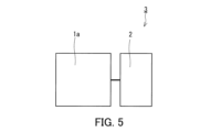
- FIG. 5 illustrates an example embodiment of a sensor.
- FIG. 6 is a perspective view showing another example of the embodiment of the thermoelectric conversion element.
- FIG. 7 is a diagram showing a schematic diagram of a method for measuring the internal stress of a thermoelectric converter.
- the thermoelectric conversion element 1a includes a substrate 20 and a thermoelectric converter 11.
- the thermoelectric converter 11 is disposed on a first surface S1 of the substrate 20.
- the thermoelectric converter 11 has a second surface S2 that intersects with a perpendicular line P to the first surface S1.
- at least one selected from the group consisting of the first surface S1 and the second surface S2 has a maximum height roughness Rz of 30 nm or less.
- the maximum height roughness Rz is determined, for example, in accordance with Japanese Industrial Standards (JIS) B 0601:2013.
- the first surface S1 and the second surface S2 are, for example, surfaces parallel to the XY plane.
- the X-axis, the Y-axis, and the Z-axis are mutually orthogonal, and the Z-axis is perpendicular to the first surface S1.
- thermoelectric conversion performance of a thermoelectric conversion element in which a thermoelectric converter is provided on a substrate it is advantageous to set the internal stress in the thermoelectric converter to a specified state in order to improve the thermoelectric conversion performance of a thermoelectric conversion element in which a thermoelectric converter is provided on a substrate.
- the internal stress in the thermoelectric converter is adjusted to a specified state, depending on the usage environment, cracks may occur in the thermoelectric converter due to the internal stress, and the thermoelectric conversion performance of the thermoelectric conversion element may decrease.
- cracks may occur in the thermoelectric converter if the thermoelectric conversion element is exposed to a high-temperature, high-humidity environment for a long period of time. It has been found that the occurrence of such cracks is related not only to the state of the internal stress in the thermoelectric converter, but also to the state of the surface of the substrate in contact with the thermoelectric converter.
- thermoelectric conversion element having a thermoelectric converter provided on a substrate
- a film of a precursor of the thermoelectric converter on the surface of the substrate while transporting the substrate.
- a substrate having an uneven surface is used to prevent blocking caused by the stacking of the substrates. According to the inventors' investigation, it was found that the uneven surface of the substrate is involved in the occurrence of cracks in the thermoelectric converter when the thermoelectric conversion element is exposed to a high-temperature, high-humidity environment for a long period of time.
- the inventors therefore, after much trial and error, have newly discovered that by adjusting the maximum height roughness Rz of at least one surface selected from the group consisting of the surface of the substrate in contact with the thermoelectric converter and the surface of the thermoelectric converter to a predetermined range, cracks are less likely to occur in the thermoelectric converter.
- At least one selected from the group consisting of the first surface S1 and the second surface S2 has a maximum height roughness Rz of 30 nm or less. This makes it difficult for cracks to occur in the thermoelectric conversion element, for example, even if the thermoelectric conversion element is exposed to a high-temperature, high-humidity environment for a long period of time. Therefore, the thermoelectric conversion element 1a is likely to have high durability in the usage environment.
- the maximum height roughness Rz may be 25 nm or less, 20 nm or less, or 15 nm or less, or may be, for example, 1 nm or more.
- the substrate 20 has, for example, a third surface S3.
- the third surface S3 extends parallel to the first surface S1, away from the thermoelectric conversion body 11.
- the surface state of the third surface S3 is not limited to a specific state.
- the third surface S3 has, for example, an arithmetic mean roughness Ra of 8 nm or more.
- the arithmetic mean roughness Ra of the third surface S3 may be 9 nm or more, or 10 nm or more.
- the arithmetic mean roughness Ra of the third surface S3 may be, for example, 20 nm or less, 15 nm or less, or 12 nm or less.
- the arithmetic mean roughness Ra of the third surface S3 may be included in any of the ranges determined by all combinations of a lower limit value of any one of 8 nm, 9 nm, and 10 nm and an upper limit value of any one of 20 nm, 15 nm, and 12 nm.
- the minimum internal stress ⁇ min in the thermoelectric converter 11 is not limited to a specific value.
- the minimum internal stress ⁇ min is the minimum value of the internal stress of the thermoelectric converter 11 in a plane parallel to the first surface S1.
- the minimum internal stress ⁇ min is, for example, -300 MPa or less. In this case, the thermoelectric conversion performance of the thermoelectric conversion element 1a is likely to be high.
- a positive internal stress indicates a tensile stress
- a negative internal stress indicates a compressive stress.
- the minimum internal stress ⁇ min being -300 MPa or less indicates that a relatively large compressive stress exists as an internal stress in the thermoelectric converter 11.
- thermoelectric conversion element 1a When the thermoelectric conversion element is exposed to a high-temperature and high-humidity environment for a long period of time, such compressive stress, in combination with the unevenness of the surface of the substrate, tends to cause cracks in the thermoelectric converter.
- the maximum height roughness Rz of at least one surface selected from the group consisting of the first surface S1 and the second surface S2 is 30 nm or less, cracks are unlikely to occur in the thermoelectric converter 11 even if the minimum internal stress ⁇ min is -300 MPa or less. Therefore, the thermoelectric conversion element 1a tends to have high durability in the usage environment.
- the minimum internal stress ⁇ min is, for example, ⁇ 900 MPa or more.
- the minimum internal stress ⁇ min may be included in any of the ranges determined by all combinations of any one of the upper limit values of ⁇ 300 MPa, ⁇ 350 MPa, ⁇ 400 MPa, ⁇ 450 MPa, ⁇ 500 MPa, ⁇ 550 MPa, and ⁇ 600 MPa and any one of the lower limit values of ⁇ 900 MPa, ⁇ 850 MPa, ⁇ 800 MPa, ⁇ 750 MPa, and ⁇ 700 MPa.
- the thermoelectric converter 11 is, for example, a thin wire 11a containing a magnetic material. With this configuration, for example, the thermoelectric converter element 1a is likely to exhibit the desired thermoelectric conversion performance due to the thermoelectric conversion characteristics of the magnetic material.
- the thermoelectric converter 11 includes, for example, a plurality of thin wires 11a.
- the thin wire 11a extends, for example, along the Y-axis direction.
- the thickness which is the dimension of the thin wire 11a in the Z-axis direction, is not limited to a specific value.
- the thickness is, for example, 1000 nm or less. This allows the amount of material used for the thin wire 11a to be reduced, making it easier to reduce the manufacturing costs of the thermoelectric conversion element 1a. In addition, breaks are less likely to occur in the thermoelectric conversion body 11.
- the thickness of the thin wire 11a is, for example, 5 nm or more. This makes it easier for the thermoelectric conversion element 1a to exhibit high durability.
- the thickness of the thin wire 11a may be included in any of the ranges determined by all combinations of a lower limit value of any one of 5 nm, 10 nm, 20 nm, 30 nm, and 50 nm and an upper limit value of any one of 1000 nm, 750 nm, 500 nm, 400 nm, 300 nm, and 200 nm.
- the width which is the dimension of the thin wire 11a in the X-axis direction, is not limited to a specific value.
- the width of the thin wire 11a is, for example, 500 ⁇ m or less. This allows the amount of material used for the thin wire 11a to be reduced, making it easier to reduce the manufacturing costs of the thermoelectric conversion element 1a.
- the width of the thin wire 11a is, for example, 1 ⁇ m or more. This makes it less likely for breaks to occur in the thin wire 11a, making it easier for the thermoelectric conversion element 1a to have high durability.
- the width of the fine wire 11a may be included in any of the ranges determined by all combinations of a lower limit of 1 ⁇ m, 2 ⁇ m, 5 ⁇ m, 10 ⁇ m, 20 ⁇ m, and 30 ⁇ m and an upper limit of 500 ⁇ m, 400 ⁇ m, 300 ⁇ m, 200 ⁇ m, 100 ⁇ m, and 50 ⁇ m.
- between the first internal stress ⁇ Y and the second internal stress ⁇ X of the thermoelectric converter 11 is not limited to a specific value.
- the first internal stress ⁇ Y is the internal stress of the thermoelectric converter 11 in the length direction (Y-axis direction) of the thin wire 11a.
- the second internal stress ⁇ X is the internal stress of the thermoelectric converter 11 in the width direction (X-axis direction) of the thin wire 11a.
- is, for example, 50 MPa or more.
- the magnetic properties of the magnetic material contained in the thin wire 11a tend to have large anisotropy in the length direction and width direction, and the thermoelectric converter 11 tends to have the desired thermoelectric conversion properties. Therefore, the thermoelectric conversion element 1a tends to exhibit the desired thermoelectric conversion performance.
- the thin wire 11a extends linearly in the Y-axis direction. Therefore, when considering the shape magnetic anisotropy, it seems that in the thermoelectric converter 11, an easy axis of magnetization occurs in the length direction of the thin wire 11a, and a hard axis of magnetization occurs in the width direction of the thin wire 11a.
- in the thermoelectric converter 11 is 50 MPa or more, the magnetic properties of the magnetic material contained in the thin wire 11a tend to have large anisotropy in the length direction and width direction.
- ⁇ is the magnetostriction constant of the magnetic material
- ⁇ indicates the internal stress of the magnetic material.
- the anisotropy of the magnetic properties of the magnetic material in the length direction and width direction of the thin wire 11a increases as the difference ⁇ X - ⁇ Y has a larger positive value when the magnetostriction constant ⁇ is a positive value, or as the difference ⁇ X - ⁇ Y has a smaller negative value when the magnetostriction constant ⁇ is a negative value.
- FIG. 3 is a graph showing the relationship between the magnetization of the thermoelectric converter 11 and an external magnetic field.
- the solid line graph shows the relationship between the magnetization of the thermoelectric converter 11 in the width direction (X-axis direction) of the thin wire 11a and the external magnetic field.
- the dashed line graph shows the relationship between the magnetization of the thermoelectric converter 11 in the length direction (Y-axis direction) of the thin wire 11a and the external magnetic field.
- is 50 MPa or more, so that the magnetic properties of the thermoelectric converter 11 have large anisotropy in the length direction and width direction of the thin wire 11a.
- thermoelectric converter 11 Due to such large anisotropy of the magnetic properties, in the thermoelectric converter 11, a magnetization hard axis is generated in the length direction of the thin wire 11a, and a magnetization easy axis is easily generated in the width direction of the thin wire 11a. As a result, the thermoelectric converter 11 is likely to exhibit stable behavior against an external magnetic field, and the thermoelectric conversion element 1a is likely to exhibit the desired thermoelectric conversion performance.
- the magnetic material contained in the thin wire 11a preferably has an axis of easy magnetization in the width direction of the thin wire 11a.
- may be 100 MPa or more, 150 MPa or more, or 200 MPa or more.
- is not limited to a specific value.
- is, for example, 900 MPa or less. In this case, even if a bending load in the width is applied to both ends of the thin wire 11a, cracks are unlikely to occur in the thermoelectric converter 11.
- the first internal stress ⁇ Y may be a tensile stress or a compressive stress.
- the first internal stress ⁇ Y may be included in any of the ranges determined by all combinations of a lower limit value of any one of ⁇ 900 MPa, ⁇ 700 MPa, ⁇ 500 MPa, and ⁇ 300 MPa and an upper limit value of any one of 900 MPa, 700 MPa, 500 MPa, and 300 MPa.
- the second internal stress ⁇ X may be a tensile stress or a compressive stress.
- the second internal stress ⁇ X may be included in any of the ranges determined by all combinations of a lower limit value of any one of ⁇ 900 MPa, ⁇ 700 MPa, ⁇ 500 MPa, and ⁇ 300 MPa and an upper limit value of any one of 900 MPa, 700 MPa, 500 MPa, and 300 MPa.
- the magnetostriction constant of the magnetic material contained in the thin wire 11a may be a positive value or a negative value.
- the condition ⁇ X - ⁇ Y ⁇ 50 MPa may be satisfied
- the condition ⁇ Y - ⁇ X ⁇ 50 MPa may be satisfied.
- the first internal stress ⁇ Y may be the minimum internal stress ⁇ min
- the second internal stress ⁇ X may be the minimum internal stress ⁇ min .
- the squareness ratio determined by the M-H curve in the width direction of the thin wire 11a of the thermoelectric converter 11 is not limited to a specific value.
- the squareness ratio is the ratio Mr/Ms of the residual magnetization Mr to the saturation magnetization Ms in the M-H curve.
- the squareness ratio is, for example, 80% or more. This makes it easier for the thermoelectric conversion element 1a to exhibit the desired thermoelectric conversion performance.
- the squareness ratio may be 85% or more, or may be 90% or more.
- thermoelectric converter 11 generates an electromotive force in the length direction (Y-axis direction) of the thin wire 11a due to, for example, a temperature gradient ⁇ T in a direction (Z-axis direction) perpendicular to the first surface S1.
- the electromotive force generated by thermoelectric conversion can be adjusted by adjusting the length of the thin wire 11a, and the thermoelectric conversion element 1a can be used for various purposes.
- Thermoelectric converter 11 generates an electromotive force, for example, by the magneto-thermoelectric effect.
- the magneto-thermoelectric effect is, for example, the anomalous Nernst effect.
- the thermoelectric converter 11 contains, for example, a substance exhibiting the anomalous Nernst effect.
- the substance exhibiting the anomalous Nernst effect is not limited to a specific substance.
- the substance exhibiting the anomalous Nernst effect is, for example, a magnetic substance having a saturation magnetic susceptibility of 5 ⁇ 10 ⁇ 3 T or more or a substance having a band structure with a Weyl point in the vicinity of the Fermi energy.
- the magnetic substance may be a ferrimagnetic substance.
- the thermoelectric converter 11 contains, for example, at least one substance selected from the group consisting of the following (i), (ii), (iii), (iv), and (v) as the substance exhibiting the anomalous Nernst effect.
- a stoichiometric substance having a composition represented by Fe3X (i) a stoichiometric substance having a composition represented by Fe3X ; (ii) an off-stoichiometric substance in which the composition ratio of Fe and X deviates from that of the substance (i) above; (iii) a substance in which part of the Fe sites of the substance (i) above or part of the Fe sites of the substance (ii) above is substituted with a typical metal element or transition element other than X; (iv) a substance having a composition represented by Fe3M11 -xM2x ( 0 ⁇ x ⁇ 1), in which M1 and M2 are different typical elements; (v) a substance in which part of the Fe sites of the substance (i) above is substituted with a transition element other than X, and part of the X sites of the substance (i) above is substituted with a typical metal element other than X.
- X is a typical element or a transition element.
- X is, for example, Al, Ga, Ge, Sn, Si, Ti, Zr, Hf, V, Nb, Ta, Cr, Mo, W, Sc, Ni, Mn, or Co.
- the combination of M1 and M2 is not limited to a specific combination as long as M1 and M2 are different typical elements.
- the combination of M1 and M2 is, for example, Ga and Al, Si and Al, or Ga and B.
- the thermoelectric converter 11 may contain Co 2 MnGa or Mn 3 Sn as a substance exhibiting the anomalous Nernst effect.
- the magnetostriction constant ⁇ of the magnetic material contained in the thin wire 11a is not limited to a specific value.
- the absolute value of the magnetostriction constant ⁇ is, for example, 5 ⁇ 10 ⁇ 6 or more.
- the absolute value of the magnetostriction constant ⁇ may be 10 ⁇ 10 ⁇ 6 or more, or may be 20 ⁇ 10 ⁇ 6 or more.
- the thermoelectric conversion element 1a has a meander pattern including the thermoelectric conversion body 11.
- the total length of the fine wires 11a included in the thermoelectric conversion element 1a tends to be large.
- the electromotive force generated in the length direction of the fine wires 11a due to the temperature gradient ⁇ T in the direction perpendicular to the first surface S1 tends to be large as the total length of the fine wires 11a is large.
- the thermoelectric conversion element 1a have a meander pattern including the thermoelectric conversion body 11, the electromotive force generated in the thermoelectric conversion element 1a tends to be large.
- the thermoelectric conversion element 1a further includes, for example, wiring 12.
- the wiring 12 electrically connects the fine wires 11a to each other.
- the wiring 12 electrically connects the multiple fine wires 11a in the thermoelectric conversion body 11 in series.
- the wiring 12 includes, for example, multiple wirings 12a.
- the multiple fine wires 11a and the multiple wirings 12a are electrically connected in series. With this configuration, even if the area of the surface on which the multiple fine wires 11a and the multiple wirings 12a are arranged is small, a large electromotive force is likely to be generated in the thermoelectric conversion element 1a.
- the wiring 12 may be made of a single metal or an alloy.
- the multiple fine wires 11a and multiple wirings 12a are arranged, for example, to form the meander pattern described above.
- one end 15p and the other end 15q of the conductive path 15 can be connected to external wiring to extract the electromotive force generated in the thermoelectric conversion element 1a to the outside.
- a heat flow can be generated in the thickness direction of the substrate 20 by applying a voltage between one end 15p and the other end 15q.
- the thin wires 11a are, for example, spaced apart at a predetermined interval in the X-axis direction and arranged parallel to one another.
- the thin wires 11a are, for example, arranged at equal intervals in the X-axis direction.
- the wiring 12a electrically connects, for example, the thin wires 11a adjacent to one another in the X-axis direction.
- the wiring 12a electrically connects, for example, one end of the thin wire 11a in the Y-axis direction to the other end in the Y-axis direction of another thin wire 11a adjacent to that thin wire 11a.
- One end of the thin wires 11a in the Y-axis direction is located at the end on the same side of the thin wire 11a in the Y-axis direction, and the other end of the thin wires 11a in the Y-axis direction is located at the end opposite to the one end of the thin wire 11a in the Y-axis direction.
- the thickness which is the dimension of the wiring 12a in the Z-axis direction, is not limited to a specific value.
- the thickness may be included in any of the ranges determined by all combinations of a lower limit value of any one of 5 nm, 10 nm, 20 nm, 30 nm, and 50 nm and an upper limit value of any one of 1000 nm, 750 nm, 500 nm, 400 nm, 300 nm, and 200 nm.
- the width of the wiring 12a is not limited to a specific value.
- the width may be included in any of the ranges determined by all combinations of a lower limit of 0.1 ⁇ m, 0.5 ⁇ m, 1 ⁇ m, 2 ⁇ m, 5 ⁇ m, 10 ⁇ m, 20 ⁇ m, and 30 ⁇ m and an upper limit of 500 ⁇ m, 400 ⁇ m, 300 ⁇ m, 200 ⁇ m, 100 ⁇ m, and 50 ⁇ m.
- the substrate 20 is not limited to a specific substrate, so long as at least one surface selected from the group consisting of the first surface S1 and the second surface S2 has a maximum height roughness Rz of 30 nm or less.
- the substrate 20 contains, for example, an organic material. With this configuration, it is easy to adjust the internal stress in the thermoelectric converter 11 to a desired state from the perspective of thermoelectric conversion performance. In addition, it is easy to reduce the manufacturing cost of the thermoelectric conversion element 1a.
- the substrate 20 contains, for example, an organic polymer as an organic material.
- organic polymer examples include polyethylene terephthalate (PET), polyethylene naphthalate (PEN), acrylic resin (PMMA), polycarbonate (PC), polyimide (PI), or cycloolefin polymer (COP).
- the thickness of the substrate 20 is not limited to a specific value.
- the thickness is, for example, 10 to 250 ⁇ m.
- the substrate 20 has, for example, flexibility.
- the substrate 20 has elasticity that allows the test piece to be elastically deformed when, for example, a strip-shaped test piece made from the substrate 20 is wound around a cylindrical mandrel having a diameter of 10 cm so that both ends in the longitudinal direction of the test piece face in the same direction.
- between the second dimensional change rate C X and the first dimensional change rate C Y of the substrate 20 is not limited to a specific value.
- the first dimensional change rate C Y is a value obtained by dividing the dimension at 25 ° C. after the test in the length direction (Y-axis direction) of the thin wire 11a along the first surface S1 by the dimension at 25 ° C. before the test when the substrate 20 is heated at 150 ° C. for 30 minutes.
- the second dimensional change rate C X is a value obtained by dividing the dimension at 25 ° C. after the above test in the width direction (X-axis direction) of the thin wire 11a by the dimension at 25 ° C. before the test.
- is, for example, 0.10% or more.
- a predetermined heat treatment is performed in a state in which the precursor of the thermoelectric converter 11 is formed on the first surface S1 of the substrate 20, so that the degree of contraction of the substrate 20 after the heat treatment differs in the length direction and width direction of the thin wire 11a. This makes it easy to adjust the internal stress in the thermoelectric converter 11 to a desired state from the viewpoint of thermoelectric conversion performance.
- may be 0.2% or more, 0.3% or more, 0.4% or more, or 0.5% or more, for example, 10% or less.
- the first surface S1 of the substrate 20 may be formed by a surface layer such as a hard coat layer.
- thermoelectric conversion element 1a is manufactured, for example, by a method including the following steps (I) and (II).
- steps (I) and (II) A precursor of the thermoelectric converter 11 is formed on the first surface S1 of the substrate 20.
- steps (II) The substrate 20 and the precursor of the thermoelectric converter 11 are heat-treated at a predetermined temperature.
- a film of the precursor of the thermoelectric converter 11 is formed on the first surface S1 of the substrate 20 by, for example, sputtering, chemical vapor deposition (CVD), pulsed laser deposition (PLD), ion plating, plating, or other methods.
- CVD chemical vapor deposition
- PLD pulsed laser deposition
- ion plating plating, or other methods.
- a photoresist is applied onto the film, a photomask is placed on the film, exposure is performed, and then wet etching is performed.
- a plurality of thin wires of the precursor of the thermoelectric converter 11 arranged at a predetermined interval are formed.
- a film of the precursor of the wiring 12 is formed on the first surface S1 of the substrate 20 by, for example, sputtering, CVD, PLD, ion plating, plating, or other methods.
- a photoresist is applied onto the film of the precursor of the wiring 12, a photomask is placed on the film of the precursor of the wiring 12, exposure is performed, and then wet etching is performed. As a result, the wiring 12 is obtained, and the thin wires of the precursor of the thermoelectric converter 11 are electrically connected to each other.
- the temperature of the heat treatment in (II) is not limited to a specific temperature.
- the ambient temperature of the substrate 20 and the precursor of the thermoelectric converter 11 during the heat treatment is, for example, 50°C or higher. This makes it easier to adjust the internal stress of the thermoelectric converter 11 to a desired state from the perspective of thermoelectric conversion performance.
- the ambient temperature of the substrate 20 and the precursor of the thermoelectric converter 11 during the heat treatment may be 100°C or higher, 150°C or higher, or 200°C or higher.
- the ambient temperature is, for example, 300°C or lower.
- the time during which the ambient temperature of the substrate 20 is maintained at 50°C or higher during the heat treatment is not limited to a specific value.
- the time is, for example, 10 minutes or more and 3 hours or less.
- thermoelectric converter element 1a is manufactured.
- thermoelectric conversion element 1a may be provided, for example, together with an adhesive layer.
- the substrate 20 is disposed between the thermoelectric conversion body 11 and the adhesive layer in the thickness direction of the substrate 20. This allows the adhesive layer to be pressed against an article, thereby attaching the thermoelectric conversion element 1a to the article.
- the adhesive layer contains, for example, a rubber-based adhesive, an acrylic-based adhesive, a silicone-based adhesive, or a urethane-based adhesive.
- the thermoelectric conversion element 1a may be provided together with an adhesive layer and a release liner.
- the release liner covers the adhesive layer.
- the release liner is typically a film that can maintain the adhesive force of the adhesive layer when covering the adhesive layer, and can be easily peeled off from the adhesive layer.
- the release liner is, for example, a film made of a polyester resin such as PET.
- the adhesive layer is exposed by peeling off the release liner, and the thermoelectric conversion element 100 can be attached to an article.
- thermoelectric conversion element 1a may be provided in a wound structure 5.
- the film- or sheet-shaped thermoelectric conversion element 1a is wound around the side of a cylindrical or columnar core 4 to obtain the wound structure 5.
- a sensor 3 equipped with a thermoelectric conversion element 1a can be provided.
- this sensor 3 for example, when a temperature gradient ⁇ T occurs in the thickness direction of the substrate 20, an electromotive force is generated in the length direction of the thin wire 11a.
- the sensor 3 can sense heat by processing an electrical signal output to the outside of the thermoelectric conversion element 1a based on this electromotive force.
- the sensor 3 further includes, for example, a signal processing device 2.
- the electrical signal output to the outside of the thermoelectric conversion element 1a is processed in the signal processing device 2.
- Thermoelectric conversion element 1a can be modified from various viewpoints.
- Thermoelectric conversion element 1a may be modified, for example, to thermoelectric conversion element 1b shown in FIG. 6.
- Thermoelectric conversion element 1b is configured in the same manner as thermoelectric conversion element 1a, except for the parts that will be specifically described.
- the components of thermoelectric conversion element 1b that are the same as or correspond to the components of thermoelectric conversion element 1a are given the same reference numerals, and detailed description will be omitted.
- the description of thermoelectric conversion element 1a also applies to thermoelectric conversion element 1b, unless there is a technical contradiction.
- thermoelectric conversion body 11 extends continuously on, for example, the first surface S1.
- the wiring 12 is disposed on a portion of the thermoelectric conversion body 11.
- the multiple wirings 12a included in the wiring 12 are disposed on the thermoelectric conversion body 11 at a predetermined interval from each other.
- thermoelectric conversion body 11 has, for example, a meander pattern.
- thermoelectric conversion element 1b is configured such that a single layer of the thermoelectric conversion body 11 and a laminate including the thermoelectric conversion body 11 and the wiring 12a appear alternately in the X-axis direction.
- Example 1 A thin film having a thickness of 96 nm was formed on the hard coat layer of a polyethylene terephthalate (PET) film A having a total thickness of 54 ⁇ m and a hard coat layer having a thickness of 4 ⁇ m as a surface layer by DC magnetron sputtering using a target material containing Fe and Ga.
- argon gas was supplied as a process gas at a pressure of 0.1 Pa.
- the relationship of Fe content:Ga content 3:1 was satisfied in terms of atomic ratio.
- the temperature around the PET film A was adjusted to 100 ° C.
- the PET film A on which the thin film was formed was heat-treated for 30 minutes in an environment of 150 ° C.
- a photoresist was applied on the thin film, a photomask was placed on the thin film, and exposure was performed, followed by wet etching.
- 115 FeGa-containing thin wires arranged at a predetermined interval were formed.
- the width of each FeGa-containing thin wire was 40 ⁇ m, and the length of each FeGa-containing thin wire was 1.5 cm.
- a Cu thin film having a thickness of 100 nm was formed on the hard coat layer of the PET film A by DC magnetron sputtering using a target material containing Cu.
- a photoresist was applied onto the Cu thin film, and a photomask was placed on the Cu thin film to perform exposure, followed by wet etching.
- thermoelectric conversion element of Example 1 was produced.
- the vertical direction (TD) of PET film A coincided with the width direction of the FeGa-containing thin wire.
- thermoelectric conversion element according to Comparative Example 1 was produced in the same manner as in Example 1, except that PET film B having a total thickness of 50 ⁇ m and no hard coat layer was used instead of PET film A.
- thermoelectric conversion element according to Comparative Example 1 was produced in the same manner as in Example 1, except for the following points.
- the PET film B used in Comparative Example 1 was used instead of the PET film A.
- the pressure of the argon gas supplied as the process gas in the DC magnetron sputtering was adjusted to 1.6 Pa.
- thermoelectric conversion element according to Comparative Example 3 was produced in the same manner as in Example 1, except that a PET film C different from the PET films used in Example 1 and Comparative Example 1 was used.
- Magnetic properties The magnetic properties of the FeGa-containing thin wire of the thermoelectric conversion element according to each example and each comparative example were measured using a small refrigerant-free physical property measurement system PPMS-versalab from Qantum Design. For this measurement, a measurement sample was used that was prepared by cutting out the part of the module according to each example and each comparative example where the conductive path was arranged into a 2 mm square.
- VSM Vibration Sample Magnetrometer
- the first internal stress ⁇ Y was the internal stress in the length direction of the FeGa-containing thin wire
- the second internal stress ⁇ X was the internal stress in the width direction parallel to the main surface of the PET film and perpendicular to the length direction of the FeGa-containing thin wire.
- the wavelength ⁇ of the Cu-K ⁇ rays was 0.1541 nm.
- the integration time at each measurement point was set to 100 seconds.
- the crystal lattice spacing d of the magnetic material at each measurement angle ( ⁇ ) was calculated from the peak angle 2 ⁇ of the obtained X-ray diffraction and the wavelength ⁇ of the X-ray irradiated from the light source, and the crystal lattice distortion ⁇ was calculated from the crystal lattice spacing d according to the relationship of the following formulas (1) and (2).
- the above-mentioned X-ray diffraction measurement was performed in each case where the angle ( ⁇ ) between the normal to the main surface of the sample Sa and the normal to the crystal plane of the crystal Mb was 0°, 17°, 24°, 30°, 35°, 40°, and 45°, and the crystal lattice strain ⁇ at each angle ( ⁇ ) was calculated. Then, the first internal stress ⁇ Y and the second internal stress ⁇ X were calculated from the slope of the line plotting the relationship between sin 2 ⁇ and the crystal lattice strain ⁇ using the following formula (3). The results are shown in Table 1. In the internal stress in Table 1, positive values indicate tensile stress and negative values indicate compressive stress.
- E is the Young's modulus of the magnetic material (130 GPa)
- ⁇ is the Poisson's ratio of the magnetic material (0.3).
- Detector D in Figure 7 detects X-ray diffraction.
- thermoelectric conversion elements according to each of the examples and comparative examples were subjected to a high temperature and humidity environmental test for 120 hours at a temperature of 85° C. and a relative humidity of 85%.
- the electrical resistance R 0 of the conductive path before the high temperature and humidity environmental test, the electrical resistance R 24 of the conductive path 24 hours after the start of the high temperature and humidity environmental test, and the electrical resistance R 120 of the conductive path after the high temperature and humidity environmental test were measured.
- the electrical resistance R 24 or the electrical resistance R 120 was 1.5 times or more the electrical resistance R 0 , it was determined that the conductive path had been broken.
- Table 1 The results are shown in Table 1.
- Example 1 As shown in Table 1, in Example 1, no breaks were found in the conductive path even after 120 hours of high temperature and high humidity environmental testing. On the other hand, in each of the comparative examples, breaks were found in the conductive path after 120 hours of high temperature and high humidity environmental testing. Comparing Example 1 with each of the comparative examples, it was suggested that high durability can be exhibited over a long period of time in high temperature and high humidity environmental testing because the maximum height roughness Rz of the surface on which the FeGa-containing fine wires of each PET film are formed or the surface of the FeGa fine wires is 30 nm or less.
- Comparative Example 1 no breaks in the conductive path were observed 24 hours after the start of the high-temperature, high-humidity environment test.
- Comparative Example 2 breaks in the conductive path were observed 24 hours after the start of the high-temperature, high-humidity environment test.
- Comparative Example 2 a relatively large tensile internal stress was generated in the FeGa-containing thin wire, and cracks were generated in the FeGa-containing thin wire due to the tensile stress generated by the expansion of the PET film caused by exposure to the high-temperature, high-humidity environment.
- Comparative Example 1 a compressive internal stress was generated in the FeGa-containing thin wire, and the FeGa-containing thin wire was able to withstand the tensile stress generated by the expansion of the PET film caused by exposure to the high-temperature, high-humidity environment and did not crack.
- the PET film was exposed to the high-temperature, high-humidity environment for 120 hours, the vicinity of the interface between the FeGa-containing thin wire and the PET film deteriorated, reducing the adhesion between them, and it is believed that the compressive stress in the FeGa-containing thin wire caused buckling, resulting in cracks in the FeGa-containing thin wire.
- Comparative Example 3 breakage of the conductive path was confirmed 24 hours after the start of the high-temperature, high-humidity environmental test. Comparing Example 1 and Comparative Example 3, it can be seen that in order to exhibit high durability over a long period of time in the high-temperature, high-humidity environmental test, it is desirable for the difference
- the first aspect of the present invention is A substrate; a thermoelectric converter disposed on a first surface of the substrate and having a second surface that intersects with a perpendicular line to the first surface; At least one selected from the group consisting of the first surface and the second surface has a maximum height roughness Rz of 30 nm or less; A thermoelectric conversion element is provided.
- a second aspect of the present disclosure is the substrate has a third surface extending parallel to the first surface and away from the thermoelectric conversion body;
- the third surface has an arithmetic average roughness Ra of 8 nm or more.
- a thermoelectric conversion element according to a first aspect is provided.
- thermoelectric converter has a minimum internal stress of ⁇ 300 MPa or less, The minimum internal stress is a minimum value of the internal stress of the thermoelectric converter in a plane parallel to the first surface.
- a thermoelectric conversion element according to a first or second aspect is provided.
- thermoelectric converter is a thin wire containing a magnetic material.
- thermoelectric conversion element according to any one of the first to third aspects is provided.
- a fifth aspect of the present disclosure is A difference between a first internal stress of the thermoelectric converter in the length direction of the thin wire and a second internal stress of the thermoelectric converter in a width direction perpendicular to the length direction and parallel to the first surface is 50 MPa or more. According to a fourth aspect, a thermoelectric conversion element is provided.
- thermoelectric converter generates an electromotive force in a longitudinal direction of the thin wire due to a temperature gradient in a direction perpendicular to the first surface.
- thermoelectric conversion element according to a fourth or fifth aspect is provided.
- thermoelectric conversion element has a meander pattern including the thermoelectric conversion body.
- a thermoelectric conversion element according to any one of the first to seventh aspects is provided.
- a tenth aspect of the present disclosure is a method for producing a method for a semiconductor device comprising: A thermoelectric conversion element according to any one of the first to ninth aspects is provided. A sensor is provided.
Landscapes
- Physics & Mathematics (AREA)
- General Physics & Mathematics (AREA)
- Chemical & Material Sciences (AREA)
- Engineering & Computer Science (AREA)
- Combustion & Propulsion (AREA)
- Measuring Temperature Or Quantity Of Heat (AREA)
Priority Applications (2)
| Application Number | Priority Date | Filing Date | Title |
|---|---|---|---|
| JP2025510183A JPWO2024203138A1 (https=) | 2023-03-31 | 2024-03-07 | |
| CN202480017612.3A CN120858671A (zh) | 2023-03-31 | 2024-03-07 | 热电转换元件及传感器 |
Applications Claiming Priority (2)
| Application Number | Priority Date | Filing Date | Title |
|---|---|---|---|
| JP2023057432 | 2023-03-31 | ||
| JP2023-057432 | 2023-03-31 |
Publications (1)
| Publication Number | Publication Date |
|---|---|
| WO2024203138A1 true WO2024203138A1 (ja) | 2024-10-03 |
Family
ID=92904360
Family Applications (1)
| Application Number | Title | Priority Date | Filing Date |
|---|---|---|---|
| PCT/JP2024/008894 Ceased WO2024203138A1 (ja) | 2023-03-31 | 2024-03-07 | 熱電変換素子及びセンサ |
Country Status (3)
| Country | Link |
|---|---|
| JP (1) | JPWO2024203138A1 (https=) |
| CN (1) | CN120858671A (https=) |
| WO (1) | WO2024203138A1 (https=) |
Citations (3)
| Publication number | Priority date | Publication date | Assignee | Title |
|---|---|---|---|---|
| JP2022129848A (ja) * | 2021-02-25 | 2022-09-06 | 国立大学法人東北大学 | 磁性材料、積層体及び積層体の製造方法並びに熱電変換素子及び磁気センサ |
| WO2023276956A1 (ja) * | 2021-06-30 | 2023-01-05 | 株式会社村田製作所 | 熱電変換デバイス |
| WO2023277028A1 (ja) * | 2021-06-30 | 2023-01-05 | 株式会社村田製作所 | 熱電体、熱電体の製造方法、熱電デバイス、及び、熱電デバイスの製造方法 |
-
2024
- 2024-03-07 JP JP2025510183A patent/JPWO2024203138A1/ja active Pending
- 2024-03-07 CN CN202480017612.3A patent/CN120858671A/zh active Pending
- 2024-03-07 WO PCT/JP2024/008894 patent/WO2024203138A1/ja not_active Ceased
Patent Citations (3)
| Publication number | Priority date | Publication date | Assignee | Title |
|---|---|---|---|---|
| JP2022129848A (ja) * | 2021-02-25 | 2022-09-06 | 国立大学法人東北大学 | 磁性材料、積層体及び積層体の製造方法並びに熱電変換素子及び磁気センサ |
| WO2023276956A1 (ja) * | 2021-06-30 | 2023-01-05 | 株式会社村田製作所 | 熱電変換デバイス |
| WO2023277028A1 (ja) * | 2021-06-30 | 2023-01-05 | 株式会社村田製作所 | 熱電体、熱電体の製造方法、熱電デバイス、及び、熱電デバイスの製造方法 |
Also Published As
| Publication number | Publication date |
|---|---|
| JPWO2024203138A1 (https=) | 2024-10-03 |
| CN120858671A (zh) | 2025-10-28 |
Similar Documents
| Publication | Publication Date | Title |
|---|---|---|
| KR101744107B1 (ko) | 자기전기 센서 및 자기전기 센서의 생산을 위한 방법 | |
| Panduranga et al. | Polycrystalline Terfenol-D thin films grown at CMOS compatible temperature | |
| Jing et al. | Stress-induced self-biasing of magnetoelectric coupling in embedded Ni/PZT/FeNi composite | |
| US20240341191A1 (en) | Thermoelectric conversion element | |
| WO2024203138A1 (ja) | 熱電変換素子及びセンサ | |
| Fetisov et al. | Correlation between magnetoelectric and magnetic properties of ferromagnetic–piezoelectric structures | |
| EP4383993A1 (en) | Thermoelectric conversion element | |
| US20250241206A1 (en) | Magnetic-thin-film-equipped substrate, magnetic thermoelectric conversion element, sensor, and method for manufacturing magnetic-thin-film-equipped substrate | |
| WO2024203137A1 (ja) | モジュール及び熱流センサ | |
| Kuts et al. | Magnetoelectric effect in three-layered gradient LiNbO3/Ni/Metglas composites | |
| JP2025054928A (ja) | 熱電変換材料、熱電変換素子、体温計、及びセンサ | |
| CN121569610A (zh) | 热电转换元件及热电转换器件 | |
| EP4383992A1 (en) | Thermoelectric conversion element | |
| Stognij et al. | Influence of the state of interfaces on the magnitude of the magnetoelectric effect in Co (Ni) films on PbZr0. 45Ti0. 55O3 and GaAs substrates | |
| Muchenik et al. | Prediction of extrinsic charge, voltage, and work-conversion factors for laminated magnetoelectric composites | |
| EP4412436A1 (en) | Thermoelectric conversion element and method for manufacturing thermoelectric conversion element | |
| US20260107687A1 (en) | Thermoelectric conversion element and sensor | |
| US20250008841A1 (en) | Thermoelectric conversion element and sensor | |
| WO2025205391A1 (ja) | 磁性膜付部材、熱電変換素子、磁気デバイス、及び磁性膜付部材の製造方法 | |
| JP2025117875A (ja) | 熱電変換素子及び熱電変換素子の製造方法 | |
| WO2025115805A1 (ja) | 熱電デバイス及び積層体 | |
| Shim et al. | Magnetostrictive Performance of Electrodeposited TB X DY (1-X) FE Y Thin Filmevaluated from Microactuator | |
| Kim et al. | Thickness dependence of (001) texture evolution and magnetic properties of sputter-deposited FePt: MgO nanocomposite films | |
| Tian et al. | Self-Assembled La [sub. 0.67] Sr [sub. 0.33] MnO [sub. 3]: CeO [sub. 2] Vertically Aligned Nanocomposite Thin Films on Flexible Mica. |
Legal Events
| Date | Code | Title | Description |
|---|---|---|---|
| 121 | Ep: the epo has been informed by wipo that ep was designated in this application |
Ref document number: 24779272 Country of ref document: EP Kind code of ref document: A1 |
|
| ENP | Entry into the national phase |
Ref document number: 2025510183 Country of ref document: JP Kind code of ref document: A |
|
| WWE | Wipo information: entry into national phase |
Ref document number: 2025510183 Country of ref document: JP |
|
| WWE | Wipo information: entry into national phase |
Ref document number: 202480017612.3 Country of ref document: CN |
|
| WWP | Wipo information: published in national office |
Ref document number: 202480017612.3 Country of ref document: CN |
|
| NENP | Non-entry into the national phase |
Ref country code: DE |
|
| 122 | Ep: pct application non-entry in european phase |
Ref document number: 24779272 Country of ref document: EP Kind code of ref document: A1 |