WO2024201876A1 - 光導波路素子とそれを用いた光変調デバイス並びに光送信装置 - Google Patents
光導波路素子とそれを用いた光変調デバイス並びに光送信装置 Download PDFInfo
- Publication number
- WO2024201876A1 WO2024201876A1 PCT/JP2023/013109 JP2023013109W WO2024201876A1 WO 2024201876 A1 WO2024201876 A1 WO 2024201876A1 JP 2023013109 W JP2023013109 W JP 2023013109W WO 2024201876 A1 WO2024201876 A1 WO 2024201876A1
- Authority
- WO
- WIPO (PCT)
- Prior art keywords
- optical waveguide
- rib
- height
- width
- curvature
- Prior art date
- Legal status (The legal status is an assumption and is not a legal conclusion. Google has not performed a legal analysis and makes no representation as to the accuracy of the status listed.)
- Ceased
Links
Images



Classifications
-
- G—PHYSICS
- G02—OPTICS
- G02B—OPTICAL ELEMENTS, SYSTEMS OR APPARATUS
- G02B6/00—Light guides; Structural details of arrangements comprising light guides and other optical elements, e.g. couplings
- G02B6/10—Light guides; Structural details of arrangements comprising light guides and other optical elements, e.g. couplings of the optical waveguide type
- G02B6/12—Light guides; Structural details of arrangements comprising light guides and other optical elements, e.g. couplings of the optical waveguide type of the integrated circuit kind
- G02B6/122—Basic optical elements, e.g. light-guiding paths
Definitions
- the present invention relates to an optical waveguide element and an optical modulation device and optical transmission device using the same, and in particular to an optical waveguide element having a rib-type optical waveguide.
- optical waveguide elements such as optical modulators are widely used, which form an optical waveguide on a substrate with electro-optical effects such as lithium niobate (LN) and have a modulation electrode that modulates the light waves propagating through the optical waveguide.
- LN lithium niobate
- driver-integrated modulators such as the High Bandwidth Coherent Driver Modulator (HB-CDM)
- HB-CDM High Bandwidth Coherent Driver Modulator
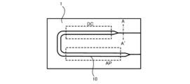
- a folded structure of the optical waveguide 10 is adopted in order to ensure as long as possible the electrode lengths of the modulation action part AP that applies a high frequency signal (RF signal) and the bias action part DC that applies a bias voltage for phase control, from the viewpoint of reducing the driving voltage.
- the electrodes that apply an electric field to the optical waveguide are not shown in order to make the shape of the optical waveguide 10 easier to see. Also, although there are multiple optical waveguides in Figure 1, only a representative optical waveguide 10 is shown.
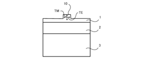
- Fig. 2 is a cross-sectional view taken along dashed line A-A' in Fig. 1.
- the LN substrate 1 on which the rib-type optical waveguide 10 is formed has a thickness of 10 ⁇ m or less, and in recent years, 1 ⁇ m or less, and in order to increase the mechanical strength, a holding substrate 3 such as Si is bonded via an intermediate layer 2 such as SiO2.
- a means for reducing the radius of curvature is, for example, to increase the effective refractive index of the optical waveguide for an optical waveguide element having a rib-type optical waveguide 10. As disclosed in Patent Document 1, this can be achieved by increasing the height and width of the ribs of the optical waveguide, thereby making it possible to increase the effective refractive index.
- the TE mode which has a large modulation efficiency (change in refractive index in response to the application of an electric field)
- the TM mode which has a large modulation efficiency (change in refractive index in response to the application of an electric field)
- the effective refractive index of the TE mode and the TM mode varies depending on the height and width of the rib-type optical waveguide. In particular, the effective refractive index of the TE mode depends on the width of the rib, and the effective refractive index of the TM mode depends on the height of the rib.
- the refractive index of the TE mode and the TM mode are equal for an optical waveguide parallel to the crystal axis Z direction, but for an optical waveguide parallel to the crystal axis Y direction, the refractive index of the TE mode is smaller than that of the TM mode due to the characteristics of the material.
- the refractive index of the material is such that the propagation speeds of the TE mode and TM mode are equal, making it easier for polarization crosstalk to occur.
- the effective refractive index of the TE mode it is necessary to make the effective refractive index of the TE mode larger than that of the TM mode, and the width of the ribs of the optical waveguide must be larger than the height of the ribs.
- the reason why the effective refractive index of the TE mode is not larger than that of the TM mode is that the process of making the rib width smaller than the height of the rib is difficult, and this prevents coupling of higher-order TM modes with the fundamental TE mode.
- the rib height or width is made larger than conventional ones, problems such as increased light scattering loss, resulting in light insertion loss, and a deterioration in the extinction ratio due to the tendency for higher-order mode light to be excited within the optical waveguide can occur.
- the problem that the present invention aims to solve is to provide an optical waveguide element that solves the problems described above, can reduce the radius of curvature of the optical waveguide, and suppresses coupling between the TE mode and the TM mode. It is also to provide an optical modulation device and an optical transmission device that use this optical waveguide element.
- the optical waveguide element, the optical modulation device, and the optical transmission device of the present invention have the following technical features.
- the relationship between the height and width of the rib-type optical waveguide is characterized in that the height value is smaller than the width value.
- the optical waveguide element described in (1) above is characterized in that, in the curvature change portion, the height and width of the rib-type optical waveguide are set to become larger as the radius of curvature becomes smaller.
- the height from the bottom surface of the substrate on which the rib-type optical waveguide is formed to the top surface of the rib of the rib-type optical waveguide is set to be constant even if the height of the rib-type optical waveguide changes.
- An optical modulation device comprising an optical waveguide element according to any one of (1) to (4) above, a housing for accommodating the optical waveguide element, and an optical fiber for inputting and outputting light waves to and from the optical waveguide element.
- the optical modulation device described in (5) above is characterized in that a modulation electrode that modulates the light wave propagating through the optical waveguide is provided on the substrate, and an electronic circuit that amplifies the modulation signal input to the modulation electrode is provided inside or outside the housing.
- An optical transmission device comprising the optical modulation device described in (6) above and an electronic circuit that outputs a modulation signal that causes the optical modulation device to perform a modulation operation.
- the rib-type optical waveguide has a straight portion and a curved portion having a constant curvature, and the straight portion and the curved portion are connected by a curvature change portion in which the curvature changes continuously.
- the straight portion and the curved portion have different heights and widths of the rib-type optical waveguide, and the curvature change portion is formed so that the height and width of the rib-type optical waveguide change continuously from the height and width of the straight portion to the height and width of the curved portion, respectively.
- FIG. 1 is a plan view showing an example of a conventional optical waveguide element.
- 2 is a cross-sectional view taken along dashed line A-A' in FIG. 1 .
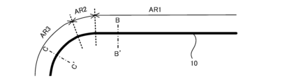
- FIG. 2 is a plan view showing a part of an optical waveguide used in the optical waveguide element of the present invention.
- 4 is a cross-sectional view taken along dashed lines B-B' and C-C' in FIG. 3.
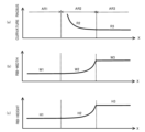
- 4 is a graph illustrating the state of change in (a) radius of curvature, (b) rib width, and (c) rib height in the optical waveguide of FIG. 3;
- 10A and 10B are diagrams showing other cross-sectional shapes of the optical waveguide used in the optical waveguide element of the present invention.
- FIG. 1 is a plan view showing an example of a conventional optical waveguide element.
- 2 is a cross-sectional view taken along dashed line A-A' in FIG. 1 .
- FIG. 2 is a plan view showing a part of an
- FIG. 2 is a plan view showing an example of a folded waveguide used in the optical waveguide element of the present invention.
- FIG. 11 is a plan view showing another example of a folded waveguide used in the optical waveguide element of the present invention.
- the present invention is characterized in that in an optical waveguide element having a rib-type optical waveguide 10, the rib-type optical waveguide has a straight portion AR1 and a curved portion AR3 formed with a constant curvature, and the straight portion AR1 and the curved portion AR3 are connected by a curvature changing portion AR2 whose curvature changes continuously, the straight portion and the curved portion have different heights and widths of the rib-type optical waveguide, and in the curvature changing portion AR2, the height and width of the rib-type optical waveguide change continuously from the height and width of the straight portion to the height and width of the curved portion, respectively.
- substrates with electro-optical effects such as lithium niobate (LN), lithium tantalate (LT), and PLZT (lead lanthanum zirconate titanate), vapor-grown films made from these materials, and even semiconductor materials and organic materials.
- LN lithium niobate
- LT lithium tantalate
- PLZT lead lanthanum zirconate titanate
- the optical waveguide 10 can be formed by etching the surface of the substrate other than the optical waveguide and forming grooves on both sides of the optical waveguide, thereby utilizing a rib-type optical waveguide in which the portion of the substrate corresponding to the optical waveguide is made convex.
- a horizontal slot waveguide that forms a slot waveguide structure in the thickness direction by thinning the substrate it is possible to reduce bending loss.
- a convex waveguide with a width or height of about 1 ⁇ m that has strong optical confinement is used.
- the substrate 1 on which the optical waveguide is formed is thinned by grinding and polishing to a thickness of 10 ⁇ m or less, more preferably 5 ⁇ m or less, and even more preferably less than 1 ⁇ m (the lower limit of the thickness is preferably 0.3 ⁇ m or more), or a smart cut method (a method of thinning by ion implantation peeling) is used to create a thin-film substrate.
- the height of the rib-type optical waveguide is preferably set to 1 ⁇ m or less. It is also possible to form a vapor-grown film on another substrate with a thickness of about the same as the above-mentioned substrate, and process the film into the shape of the above-mentioned optical waveguide.
- a substrate (thin plate, thin film) 1 on which an optical waveguide is formed is adhesively fixed to a holding substrate 3 via an intermediate layer 2 in order to increase mechanical strength.
- a composite substrate in which the thin plate, intermediate layer 2, and holding substrate 3 are integrated may be referred to as a "substrate”.
- the support substrate 3 can be made of silicon (Si) having a thickness of 1 mm or less, glass material such as alpha quartz single crystal having a low dielectric constant, quartz crystal, sapphire, or the like.
- the intermediate layer is made of a material with a lower dielectric constant than the substrate 1 in order to confine light in the substrate 1, to have a lower refractive index than the thin plate 1, and to achieve speed matching between the light wave and the electrical signal (microwave).
- a material with a thermal expansion coefficient close to that of the thin plate 1 is used.
- a silicon oxide film such as SiO2 is used with a thickness of 10 ⁇ m or less.
- the optical waveguide element of the present invention is characterized in that the straight section AR1 and the curved section AR3 of the rib-type optical waveguide have different heights and widths, and in the curvature changing section AR2 that connects the two, the height and width of the rib-type optical waveguide are formed so that they change continuously from the height and width of the straight section AR1 to the height and width of the curved section AR3.
- the ratio of the angles occupied by the curvature changing section AR2 and the curved waveguide AR3 with a constant curvature is 1:2 to 10 (degrees).
- 1:2 means that the angle occupied by the bent portion of AR2 is 30 degrees, and the angle occupied by the bent portion of AR3 is 60 degrees.
- the rib height H3 of the curved portion is greater than the rib height H1 of the straight portion
- the rib width W3 of the curved portion is greater than the rib width W1 of the straight portion.
- the radius of curvature of the curved portion by adopting this configuration, it is possible to reduce the radius of curvature of the curved portion by about 20%. If the radius of curvature of the curved portion is 100 ⁇ m in an optical waveguide that turns the traveling direction of light 90 degrees, it is possible to reduce the radius of curvature by 20% by this method, and it is possible to reduce the size (miniaturization) of the entire optical waveguide that turns 90 degrees by 20% in both the vertical and horizontal directions.
- the relationship between the height and width of the rib-type optical waveguide 10 is set so that the height is always smaller than the width (rib height ⁇ rib width), thereby suppressing coupling between the TE mode and the TM mode. Furthermore, by setting the ratio of the rib width to the rib height of the rib-type optical waveguide (straight section W1/H1, curvature change section W2/H2, curved section W3/H3) to be W1/H1 ⁇ W2/H2 ⁇ W3/H3, it is possible to more reliably suppress coupling between both modes.
- a curved waveguide (curved section or curvature change section)
- FIG. 5 is a graph showing changes in (a) radius of curvature, (b) rib width, and (c) rib height in the straight line portion AR1, the curvature change portion AR2, and the curved portion AR3 in FIG.
- the radius of curvature changes continuously in the curvature transformation portion AR2 (radius of curvature R2), and has a constant value of radius of curvature R3 in the curved portion.
- the rib width is set so that the rib width W3 of the curved portion (constant curvature) AR3 is larger than the rib width W1 of the straight portion AR1.
- the curvature conversion portion AR2 changes continuously in accordance with the change in the radius of curvature R2 so as to continuously connect the straight portion AR1 and the curved portion AR3.
- W2 ⁇ /R2 + W1, where ⁇ is the conversion coefficient.
- the width W2 changes inversely proportional to the radius of curvature R2.
- the rib height is set so that the rib width H3 of the curved portion (constant curvature) AR3 is greater than the rib width H1 of the straight portion AR1.
- the rib height changes continuously in accordance with the change in the radius of curvature R2 so as to continuously connect the straight portion AR1 and the curved portion AR3.
- the height H2 changes inversely proportional to the radius of curvature R2.
- the height H2 and width W2 of the rib-type optical waveguide are set to increase as the radius of curvature R2 decreases.
- W3 0.3 to 7 ⁇ m
- Conversion coefficient ⁇ 1 to 200 ( ⁇ m 2 )
- Conversion coefficient ⁇ 0.2 to 20 ( ⁇ m 2 )
- the side of the rib-shaped or slot-shaped optical waveguide is not perpendicular to the bottom surface of the LN substrate, but is shaped so as to be inclined toward the center of the optical waveguide, as shown in Figure 6.
- the height TH from the bottom surface of the substrate 1 forming the rib-type optical waveguide 10 to the top surface of the rib of the rib-type optical waveguide is set to be constant even if the height (H1, H3) of the rib-type optical waveguide changes.
- the thickness of the slab waveguide SB changes. This eliminates the need to change the thickness of the substrate 1 for each part of the optical waveguide, and does not complicate the manufacturing process.
- the etching time may be adjusted depending on the location, or the height may be uniformly adjusted to the same height at first, and then a process of partially digging the substrate deeper using other means such as an electron beam or laser may be added.
- a process of partially digging the substrate deeper using other means such as an electron beam or laser may be added.
- the thickness of the slab waveguide SB it is possible to reduce crosstalk between adjacent optical waveguides and optical waveguide loss near the electrodes (for example, RF signal action part/DC bias action part).
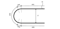
- the folded portion is formed only by the curved portion (constant curvature) AR3, and two curvature changing portions (AR2, AR4) are used to connect the two straight portions (AR1, AR5).
- the curvature can be reduced while suppressing the optical insertion loss, and the vertical space L1 can be reduced, which is effective for miniaturizing the chip.
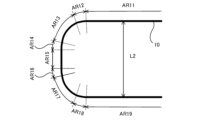
- the folded portion is composed of two curved portions (AR13, AR17) and a straight portion AR15 between them.
- a curvature change portion AR14, AR16
- a curvature change portion AR12, AR18
- the vertical space L2 can be adjusted by reducing the curvature and adjusting the length of the straight waveguide (AR15) while suppressing the optical insertion loss.
- the effect of being able to adjust the vertical space L2 is that when two parallel optical waveguides are folded back without crossing as shown in FIG.
- the vertical space of the outer optical waveguide needs to be adjusted, which is effective when adjusting the optical path length.
- the structures of FIG. 7 and FIG. 8 are adopted in the locations of structure A and structure B, respectively, and the optical path lengths of waveguides 10A and 10B can be made equal by adjusting the lengths of X_1, X_2 and Y_1, Y_2, etc.
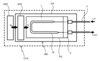
- a compact optical modulation device MD can be provided by housing the optical waveguide element (substrate 1) of the present invention in a housing CA made of metal or the like and connecting the outside of the housing to the optical waveguide element with an optical fiber F.
- a housing CA made of metal or the like
- reference numeral 5 denotes a reinforcing member superimposed on substrate 1 along the end face of substrate 1, and is used when directly joining an optical component such as an optical fiber to the end face of substrate 1.
- An electronic circuit that outputs a modulation signal S0 that causes the optical modulation device MD to perform a modulation operation can be connected to the optical modulation device MD to configure an optical transmission device OTA. Since the modulation signal S to be applied to the optical waveguide element needs to be amplified, a driver circuit DRV is used.
- the driver circuit DRV and the digital signal processor DSP can be placed outside the housing CA, but can also be placed inside the housing CA. In particular, by placing the driver circuit DRV inside the housing, the propagation loss of the modulation signal from the driver circuit can be further reduced and a wider bandwidth can be achieved.
- an optical waveguide element that can reduce the radius of curvature of the optical waveguide and suppress the coupling between the TE mode and the TM mode.
- an optical modulation device and an optical transmission device that use an optical waveguide element having such excellent effects.
Landscapes
- Physics & Mathematics (AREA)
- Engineering & Computer Science (AREA)
- Microelectronics & Electronic Packaging (AREA)
- General Physics & Mathematics (AREA)
- Optics & Photonics (AREA)
- Optical Integrated Circuits (AREA)
Abstract
Description
(1) リブ型光導波路を有する光導波路素子において、該リブ型光導波路は、直線部分と一定の曲率で構成される曲線部分とを有し、かつ該直線部分と該曲線部分との間は曲率が連続して変化する曲率変換部分で接続されており、該直線部分と該曲線部分とでは、該リブ型光導波路の高さ及び幅が異なり、該曲率変換部分では、該リブ型光導波路の高さ及び幅が、該直線部分の高さ及び幅から該曲線部分の高さ及び幅に、各々連続的に変化するように形成されていることを特徴とする。
本発明は、図3乃至5に示すように、リブ型光導波路10を有する光導波路素子において、該リブ型光導波路は、直線部分AR1と一定の曲率で構成される曲線部分AR3とを有し、かつ該直線部分AR1と該曲線部分AR3との間は曲率が連続して変化する曲率変換部分AR2で接続されており、該直線部分と該曲線部分とでは、該リブ型光導波路の高さ及び幅が異なり、該曲率変換部分AR2では、該リブ型光導波路の高さ及び幅が、該直線部分の高さ及び幅から該曲線部分の高さ及び幅に、各々連続的に変化するように形成されていることを特徴とする。
また、Tiなどを熱拡散法やプロトン交換法などで基板表面に高屈折率部分を形成する技術を、リブ型光導波路部分に合わせて適用することも可能である。特に、光導波路素子自体を小型化する場合や折り曲げた光導波路を使用する場合などには、光閉じ込めの強い、幅又は高さが1μm程度の凸状導波路を用いる。
保持基板3には、1mm以下のシリコン(Si)や誘電率の低いアルファ石英単結晶等のガラス材や水晶、サファイア等が利用可能である。
また、中間層には、基板1に光を閉じ込めるため、また、薄板1よりも屈折率が低く、光波と電気信号(マイクロ波)との速度整合を図るため、基板1よりも誘電率の低い材料が使用される。さらに、薄板1に熱応力が加わるのを抑制するため、熱膨張率が薄板1に近い材料を使用する。具体的には、SiO2などのSi酸化膜などを厚さ10μm以下で用いる。
さらに、リブ型光導波路の「リブの幅とリブの高さとの比(直線部分W1/H1,曲率変換部分W2/H2,曲線部分W3/H3)についても、W1/H1<W2/H2<W3/H3となるように設定することで、より確実に両モード間の結合を抑制することができる。さらに、曲げ導波路(曲線部分や曲率変換部分)では、基板1の長手方向(リッジの幅の方向と重なる)の実効屈折率が高くする方が光損失を抑制できるため、リブの幅方向をリブの高さよりより大きくすることが好ましい。
曲率半径は、曲率変換部分AR2(曲率半径R2)では連続的に変化し、曲線部分では曲率半径R3の一定値となる。
以上のように、曲率変換部分AR2では、曲率半径R2が小さくなるに従い、リブ型光導波路の高さH2及び幅W2はより大きくなるように設定される。曲率半径に対して、リブ高さを連続的に変化させることで、直線導波路から曲げ導波路に変換する際に、変換部の光損失を最小限に抑制することが出来る。
・基板1(LN基板)の全体の厚みTH=0.1~1μm
・直線部分のリブの高さH1=0.05~0.5μm
・直線部分のリブの幅W1=0.2~5μm
・曲線部分のリブの高さH3=0.07~0.7μm
・曲線部分のリブの幅W3=0.3~7μm
・変換係数α=1~200(μm2)
・変換係数β=0.2~20(μm2)
図7では、折り返し部分を曲線部分(曲率一定)AR3のみで形成し、2つの直線部分(AR1,AR5)とを接続する2つの曲率変換部分(AR2,AR4)を用いたものである。このような構成では、光挿入損失を抑制したまま、曲率を小さくし、縦方向のスペースL1を小さくでき、チップ小型化に有効である。
2 中間層
3 保持基板
10 光導波路(リブ型光導波路)
AR1 光導波路の直線部分
AR2 光導波路の曲率変換部分
AR3 光導波路の曲線部分(曲率一定)
Claims (7)
- リブ型光導波路を有する光導波路素子において、
該リブ型光導波路は、直線部分と一定の曲率で構成される曲線部分とを有し、かつ該直線部分と該曲線部分との間は曲率が連続して変化する曲率変換部分で接続されており、
該直線部分と該曲線部分とでは、該リブ型光導波路の高さ及び幅が異なり、
該曲率変換部分では、該リブ型光導波路の高さ及び幅が、該直線部分の高さ及び幅から該曲線部分の高さ及び幅に、各々連続的に変化するように形成されていることを特徴とする光導波路素子。 - 請求項1に記載の光導波路素子において、該リブ型光導波路の高さ及び幅の関係は、高さの値が幅の値より小さいことを特徴とする光導波路素子。
- 請求項1に記載の光導波路素子において、該曲率変換部分では、曲率半径が小さくなるに従い、該リブ型光導波路の高さ及び幅はより大きくなるように設定されていることを特徴とする光導波路素子。
- 請求項1に記載の光導波路素子において、該リブ型光導波路を形成する基板の底面から該リブ型光導波路のリブ上面までの高さは、該リブ型光導波路の高さが変化しても一定になるように設定されていることを特徴とする光導波路素子。
- 請求項1乃至4のいずれかに記載の光導波路素子と、該光導波路素子を収容する筐体と、該光導波路素子に光波を入出力する光ファイバとを有することを特徴とする光変調デバイス。
- 請求項5に記載の光変調デバイスにおいて、該光導波路を伝搬する光波を変調する変調電極を該基板に設け、該変調電極に入力する変調信号を増幅する電子回路を該筐体の内部又は外部に有することを特徴とする光変調デバイス。
- 請求項6に記載の光変調デバイスと、該光変調デバイスに変調動作を行わせる変調信号を出力する電子回路とを有することを特徴とする光送信装置。
Priority Applications (2)
| Application Number | Priority Date | Filing Date | Title |
|---|---|---|---|
| CN202380082124.6A CN120266024A (zh) | 2023-03-30 | 2023-03-30 | 光波导元件及使用其的光调制器件以及光发送装置 |
| PCT/JP2023/013109 WO2024201876A1 (ja) | 2023-03-30 | 2023-03-30 | 光導波路素子とそれを用いた光変調デバイス並びに光送信装置 |
Applications Claiming Priority (1)
| Application Number | Priority Date | Filing Date | Title |
|---|---|---|---|
| PCT/JP2023/013109 WO2024201876A1 (ja) | 2023-03-30 | 2023-03-30 | 光導波路素子とそれを用いた光変調デバイス並びに光送信装置 |
Publications (1)
| Publication Number | Publication Date |
|---|---|
| WO2024201876A1 true WO2024201876A1 (ja) | 2024-10-03 |
Family
ID=92903664
Family Applications (1)
| Application Number | Title | Priority Date | Filing Date |
|---|---|---|---|
| PCT/JP2023/013109 Ceased WO2024201876A1 (ja) | 2023-03-30 | 2023-03-30 | 光導波路素子とそれを用いた光変調デバイス並びに光送信装置 |
Country Status (2)
| Country | Link |
|---|---|
| CN (1) | CN120266024A (ja) |
| WO (1) | WO2024201876A1 (ja) |
Citations (7)
| Publication number | Priority date | Publication date | Assignee | Title |
|---|---|---|---|---|
| JPH03200904A (ja) * | 1989-12-28 | 1991-09-02 | Nec Corp | 半導体光導波路の製造方法 |
| US6028973A (en) * | 1996-09-20 | 2000-02-22 | Siemens Aktiengesellschaft | Arrangement of two integrated optical waveguides on the surface of a substrate |
| JP2001249240A (ja) * | 2000-03-06 | 2001-09-14 | Hitachi Cable Ltd | 光導波路及びその製造方法 |
| JP2017116862A (ja) * | 2015-12-25 | 2017-06-29 | 株式会社豊田中央研究所 | 光導波路 |
| WO2021117161A1 (ja) * | 2019-12-11 | 2021-06-17 | 日本電信電話株式会社 | 光導波路 |
| WO2022071283A1 (ja) * | 2020-09-30 | 2022-04-07 | 住友大阪セメント株式会社 | 光導波路素子及びそれを用いた光変調デバイス並びに光送信装置 |
| JP2022056979A (ja) * | 2020-09-30 | 2022-04-11 | 住友大阪セメント株式会社 | 光導波路素子及びそれを用いた光変調デバイス並びに光送信装置 |
-
2023
- 2023-03-30 WO PCT/JP2023/013109 patent/WO2024201876A1/ja not_active Ceased
- 2023-03-30 CN CN202380082124.6A patent/CN120266024A/zh active Pending
Patent Citations (7)
| Publication number | Priority date | Publication date | Assignee | Title |
|---|---|---|---|---|
| JPH03200904A (ja) * | 1989-12-28 | 1991-09-02 | Nec Corp | 半導体光導波路の製造方法 |
| US6028973A (en) * | 1996-09-20 | 2000-02-22 | Siemens Aktiengesellschaft | Arrangement of two integrated optical waveguides on the surface of a substrate |
| JP2001249240A (ja) * | 2000-03-06 | 2001-09-14 | Hitachi Cable Ltd | 光導波路及びその製造方法 |
| JP2017116862A (ja) * | 2015-12-25 | 2017-06-29 | 株式会社豊田中央研究所 | 光導波路 |
| WO2021117161A1 (ja) * | 2019-12-11 | 2021-06-17 | 日本電信電話株式会社 | 光導波路 |
| WO2022071283A1 (ja) * | 2020-09-30 | 2022-04-07 | 住友大阪セメント株式会社 | 光導波路素子及びそれを用いた光変調デバイス並びに光送信装置 |
| JP2022056979A (ja) * | 2020-09-30 | 2022-04-11 | 住友大阪セメント株式会社 | 光導波路素子及びそれを用いた光変調デバイス並びに光送信装置 |
Also Published As
| Publication number | Publication date |
|---|---|
| CN120266024A (zh) | 2025-07-04 |
Similar Documents
| Publication | Publication Date | Title |
|---|---|---|
| US7088875B2 (en) | Optical modulator | |
| JP5063001B2 (ja) | 進行波形光変調器 | |
| US8923658B2 (en) | Optical waveguide device | |
| US8391651B2 (en) | Optical waveguide device | |
| US11656487B2 (en) | Optical waveguide element, and optical modulation device and optical transmission apparatus using optical waveguide element | |
| US7382942B2 (en) | Optical waveguide devices | |
| US20230152660A1 (en) | Optical control element, optical modulation device using same, and optical transmission apparatus | |
| CN114185186B (zh) | 包括光调制器的光器件及光收发器 | |
| US20240319558A1 (en) | Optical waveguide element, optical modulator, optical modulation module, and optical transmission device | |
| CN100447615C (zh) | 光波导器件以及行波型光学调制器 | |
| JP2000267056A (ja) | 導波路型光デバイス | |
| US7218819B2 (en) | Electrode systems for optical modulation and optical modulators | |
| JP2022131873A (ja) | 光導波路素子及びそれを用いた光変調デバイス並びに光送信装置 | |
| WO2024201876A1 (ja) | 光導波路素子とそれを用いた光変調デバイス並びに光送信装置 | |
| WO2007058366A1 (ja) | 光導波路デバイス | |
| JP7670153B2 (ja) | 光導波路素子及びそれを用いた光変調デバイス並びに光送信装置 | |
| JP2004245991A (ja) | 光導波路デバイスおよび光導波路デバイスと光伝送部材との結合構造 | |
| US20240255783A1 (en) | Optical Waveguide Device, and Optical Modulation Device and Optical Transmission Apparatus Using Same | |
| WO2025069275A1 (ja) | 光導波路素子及びそれを用いた光変調デバイス並びに光送信装置 | |
| WO2024069952A1 (ja) | 光導波路素子及びそれを用いた光変調デバイス並びに光送信装置 | |
| WO2025203274A1 (ja) | 光導波路素子及びそれを用いた光変調器並びに光送信装置 | |
| WO2023053332A1 (ja) | 光導波路素子及びそれを用いた光変調デバイス並びに光送信装置 | |
| CN118131391A (zh) | 模式交叉抑制的集成光子芯片、制备方法器件及设备 |
Legal Events
| Date | Code | Title | Description |
|---|---|---|---|
| 121 | Ep: the epo has been informed by wipo that ep was designated in this application |
Ref document number: 23930514 Country of ref document: EP Kind code of ref document: A1 |
|
| WWE | Wipo information: entry into national phase |
Ref document number: 202380082124.6 Country of ref document: CN |
|
| WWP | Wipo information: published in national office |
Ref document number: 202380082124.6 Country of ref document: CN |
|
| NENP | Non-entry into the national phase |
Ref country code: DE |
|
| 122 | Ep: pct application non-entry in european phase |
Ref document number: 23930514 Country of ref document: EP Kind code of ref document: A1 |