WO2024201807A1 - 光回路素子 - Google Patents
光回路素子 Download PDFInfo
- Publication number
- WO2024201807A1 WO2024201807A1 PCT/JP2023/012876 JP2023012876W WO2024201807A1 WO 2024201807 A1 WO2024201807 A1 WO 2024201807A1 JP 2023012876 W JP2023012876 W JP 2023012876W WO 2024201807 A1 WO2024201807 A1 WO 2024201807A1
- Authority
- WO
- WIPO (PCT)
- Prior art keywords
- semiconductor element
- optical
- optical semiconductor
- alignment
- alignment mark
- Prior art date
- Legal status (The legal status is an assumption and is not a legal conclusion. Google has not performed a legal analysis and makes no representation as to the accuracy of the status listed.)
- Ceased
Links
Images



Classifications
-
- G—PHYSICS
- G02—OPTICS
- G02B—OPTICAL ELEMENTS, SYSTEMS OR APPARATUS
- G02B6/00—Light guides; Structural details of arrangements comprising light guides and other optical elements, e.g. couplings
- G02B6/10—Light guides; Structural details of arrangements comprising light guides and other optical elements, e.g. couplings of the optical waveguide type
- G02B6/12—Light guides; Structural details of arrangements comprising light guides and other optical elements, e.g. couplings of the optical waveguide type of the integrated circuit kind
- G02B6/122—Basic optical elements, e.g. light-guiding paths
-
- G—PHYSICS
- G02—OPTICS
- G02B—OPTICAL ELEMENTS, SYSTEMS OR APPARATUS
- G02B6/00—Light guides; Structural details of arrangements comprising light guides and other optical elements, e.g. couplings
- G02B6/24—Coupling light guides
- G02B6/42—Coupling light guides with opto-electronic elements
Definitions
- This disclosure relates to an optical circuit element, and more specifically, to an optical circuit element having a mounting groove for mounting an optical semiconductor element.
- PLC quartz-based planar lightwave circuits
- SiP silicon photonics optical circuits
- PLC is a waveguide-type optical device with excellent characteristics such as low loss, high reliability, and high design freedom.
- transmission equipment at the optical communication transmission end is equipped with PLC that integrates functions such as multiplexers/demultiplexers, branchers, and couplers.
- SiP is an optical device that can realize even smaller optical circuits because it has high design freedom, although it does not match PLC in terms of low loss.
- optical devices other than PLC and SiP such as photodiodes (hereinafter referred to as PD), laser diodes (hereinafter referred to as LD), and optical modulators that convert optical and electrical signals, can also be installed in the transmission equipment.
- PD photodiodes
- LD laser diodes
- optical modulators that convert optical and electrical signals
- a method is adopted in which a phase modulator is integrated on an InP chip, and a polarization rotator and polarization beam combiner are integrated on a PLC, and the two chips are optically coupled via a lens.
- Polarization Mux polarization multiplexer
- FIG. 1 is a conceptual diagram showing the structure of an integrated optical device 100 in which a phase modulator chip 101 and a polarization Mux chip 102 are directly connected by butting them together.
- the phase modulator chip 101 is an InP optical phase modulator chip
- the polarization Mux chip 102 is a PLC.
- the refractive index and shape of the waveguide differ due to the difference in the materials used for the waveguide. For this reason, waveguides with significantly different mode fields for the propagating light are connected, which results in large coupling losses.
- One way to eliminate coupling loss due to mode field mismatch is, for example, to introduce a spot size converter into the input/output waveguide section to bring the mode field shapes closer together.
- this method can reduce loss to a certain extent, it is difficult to perfectly match the mode field shapes between waveguides made of different materials and structures.
- optical amplification optical circuit chips are being considered that incorporate a semiconductor optical amplifier (SOA) chip on an optical circuit element and integrate the function of amplifying the intensity of the propagating signal light.
- SOA semiconductor optical amplifier
- FIG. 2 is a conceptual diagram showing the structure of an integrated optical device 200 in which a phase modulator chip 101 and an SOA-equipped polarization Mux chip 201 are butt-coupled directly.
- the integrated optical device 200 has a structure in which the polarization Mux chip 102 further includes SOAs 202a, b for optical amplification in the integrated optical device 100 shown in FIG. 1.
- the coupling loss that occurs in the end face connection between the above-mentioned different elements is compensated for by the optical amplification by the SOAs 202a, b.
- the output of the device itself can be increased, it is possible to achieve both miniaturization by end face connection and improved optical characteristics.
- the SOAs 202a, b are directly mounted on the optical circuit elements, the optical amplification function can be integrated without increasing the size of the integrated optical device.
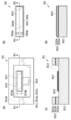
- Figure 3 is a conceptual diagram showing the respective structures of optical circuit element 301 and SOA chip 302 before mounting, with (a) showing a top view of optical circuit element 301 before mounting, (b) showing a top view of SOA chip 302 before mounting, (c) showing a cross-sectional view along line IIIc-IIIc, and (d) showing a cross-sectional view along line IIId-IIId.
- Optical circuit element 301 includes a waveguide 3012 formed on substrate 3011, and a mounting groove 3013 for mounting SOA chip 302.
- the waveguide 3012 includes an underclad 3012a, a core 3012b, and an overclad 3012c, and inside the mounting groove 3013, an electrode 3015 and a pad 3016 formed on the substrate 3011, solder 3017 arranged on the electrode 3015, and alignment marks 3018a, b for aligning the SOA chip 302 are arranged.
- the SOA chip 302 includes a waveguide 3022 formed on the substrate 3021 and including a core 3022a and a clad 3022b, a surface electrode 3023 formed on the clad 3022b, and alignment marks 3024a, b formed on the surface electrode 3023.
- the SOA 302 When mounting the SOA 302 on the optical circuit element 301 by flip-chip mounting, the SOA 302 is aligned (positioned) based on the alignment marks 3018a, b and the alignment marks 3024a, b. Then, after the waveguide 3012 of the optical circuit element 301 and the waveguide 3022 of the SOA chip 302 are aligned, the electrode 3015 of the optical circuit element 301 and the surface electrode 3023 of the SOA chip 302 are electrically connected via the solder 3017.
- an optical semiconductor element such as an SOA or LD
- alignment with a precision of less than 3 ⁇ m in waveguide distance and less than 1 ⁇ m in axial misalignment is required.
- the distance between the end face of the mounting groove on the optical circuit element for optical input/output with the SOA and the input/output end face of the SOA is extremely narrow, less than 3 ⁇ m. Therefore, in order to prevent collision between the mounting groove and the SOA during flip-chip mounting, it is necessary to move the SOA into the mounting groove with a certain degree of alignment.
- optical semiconductor elements are mainly made of compound semiconductors, and therefore are characterized by being highly brittle and easily damaged. Damage to optical semiconductor elements can be a factor in reducing the yield of device manufacturing, which can result in increased costs and reduced mounting efficiency.
- coarse alignment can also be included in which the SOA is separated from the mounting groove and each alignment mark is confirmed in a defocused position by infrared transmission.
- coarse alignment can also be performed by checking each alignment mark with upper and lower cameras. After this coarse alignment, precise alignment is performed by fine alignment while checking both alignment marks by infrared transmission.
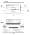
- the alignment mark must be checked at a defocused position or at a distance due to the use of upper and lower cameras, making it difficult to achieve highly accurate alignment, and as shown in Figure 4(a), misalignment of the alignment mark or rotation of the SOA may occur. If such misalignment in position or rotation occurs, the SOA may collide with the optical circuit element when it descends, as shown in Figure 4(b). Due to these factors, in the past, yields were low when mounting SOAs on optical circuit elements, preventing cost reduction and improved mounting efficiency.
- optical semiconductor elements such as SOA chips are mounted on a platform of optical circuit elements such as PLC or SiP
- This disclosure has been made in consideration of the above problems, and its purpose is to provide an optical circuit element that can achieve simple integration in hybrid integration of optical semiconductor elements on optical circuit elements, without causing the optical semiconductor elements to collide with each other when mounting the optical circuit element on the optical circuit element.
- the present disclosure provides an optical circuit element comprising a substrate, a waveguide on the substrate, and a mounting groove for mounting an optical semiconductor element on the substrate, the mounting groove having an optical semiconductor element mounting region and a pre-alignment region communicating with the optical semiconductor element mounting region, the optical semiconductor element mounting region including an end face of the waveguide on at least one side and an alignment mark on the substrate, the pre-alignment region including a pre-alignment mark on the substrate corresponding to the alignment mark, and the distance between the edge of the mounting groove in the pre-alignment region and the pre-alignment mark is greater than the distance between the edge of the mounting groove in the optical semiconductor element mounting region and the alignment mark.
- 1 is a diagram conceptually showing the structure of an integrated optical device 100 in which a phase modulator chip 101 and a polarization Mux chip 102 are butt-connected directly.
- 1 is a diagram conceptually showing the structure of an integrated optical device 200 in which a phase modulator chip 101 and an SOA-equipped polarization Mux chip 201 are butt-joined and directly coupled.
- 1A and 1B are diagrams conceptually illustrating the structures of an optical circuit element 301 and an SOA chip 302 before mounting, in which (a) is a top view of the optical circuit element 301 before mounting, (b) is a top view of the SOA chip 302 before mounting, (c) is a cross-sectional view taken along the IIIc-IIIc cross-sectional line, and (d) is a cross-sectional view taken along the IIId-IIId cross-sectional line.
- 1A and 1B are diagrams conceptually illustrating factors that cause a decrease in yield during flip-chip mounting according to the conventional technology, where FIG. 1A illustrates misalignment and rotation, and FIG. 1B illustrates collision.
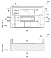
- FIG. 1A and 1B are diagrams conceptually illustrating the structure of an optical circuit element 500 according to the present disclosure, in which (a) is a top view and (b) is a cross-sectional view taken along the Vb-Vb cross-sectional line.
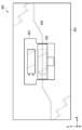
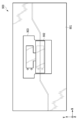
- FIG. 6 is a top view conceptually illustrating the structure of an integrated optical device 600 in which an SOA 602 is mounted on an optical circuit element 601 according to the present disclosure.
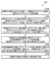
- 7 is a flowchart showing a method 700 for mounting an SOA 602 on an optical circuit element 601 according to the first embodiment.
- FIG. 8 is a top view conceptually showing the structure of an integrated optical device 800 that is an SOA-mounted SiPh according to the prior art.
- FIG. 9 is a top view conceptually illustrating the structure of an integrated optical device 900 in which an LD 902 is mounted as an optical semiconductor element on an optical circuit element 901 according to the present disclosure.
- the optical circuit element 500 includes a mounting groove 502 on a substrate 501, and the mounting groove 502 includes an optical semiconductor element mounting area 502a provided at a position that divides the waveguide 507, and a pre-alignment area 502b that communicates with the optical semiconductor element mounting area 502a.
- the optical semiconductor element mounting area 502a also includes alignment marks 503a, b and an electrode 504 on the substrate 501
- the pre-alignment area 502b includes pre-alignment marks 505a, b and a dummy electrode 506 on the substrate 501.
- the distance ⁇ between the edge of the mounting groove 502 in the pre-alignment region 502b and the pre-alignment marks 504a, b is configured to be larger than the distance ⁇ between the edge of the mounting groove 502 in the optical semiconductor element mounting region 502a and the alignment marks 503a, b.
- the pre-alignment marks 505a, b and dummy electrode 506 arranged in the pre-alignment region 502b are arranged to correspond to the alignment marks 503a, b and electrode 504 arranged in the optical semiconductor element mounting region 502a.
- the pre-alignment marks 505a, b and dummy electrode 506 can be arranged at a position obtained by shifting the positional relationship between the alignment marks 503a, b and electrode 504 in parallel in the width direction of the optical circuit element (Y direction in FIG. 5).
- the optical semiconductor element mounting region 502a of the mounting groove 502 is depicted as being arranged so as to divide the waveguide 507.
- a form in which the end faces of the waveguide 507 are included on both end faces of the mounting groove 502 corresponding to the optical semiconductor element mounting region 502a is shown, but this is for illustrative purposes only, and the end face of the waveguide 507 may be included on only one side of the mounting groove 502 corresponding to the optical semiconductor element mounting region 502a.
- the optical semiconductor element mounted in the optical semiconductor element mounting region 502a is an element that does not output light
- the optical circuit element 500 may be in such a form.
- the pre-alignment region 502b is configured to have a larger clearance than the optical semiconductor element mounting region 502a, so the possibility of collisions when mounting the optical semiconductor element is reduced compared to conventional technology.
- the optical semiconductor element is raised to a position where it does not come into contact with the electrodes 504, moved to the optical semiconductor element mounting area 502a (in the form shown in FIG. 5, moved parallel to the Y direction), and alignment is performed again, making it possible to mount the optical semiconductor element without colliding with the optical circuit element 500 and with more precise alignment than before.
- the optical circuit element 500 includes a pre-alignment region 502b adjacent to the optical semiconductor element mounting region 502a.
- the greatest feature is that in this pre-alignment region 502b, fine alignment can be performed before the optical semiconductor tissue is moved to the optical semiconductor element mounting region 502a.
- the optical semiconductor element can be lowered into the pre-alignment region 502b without colliding with the optical circuit element 500 even if there is a slight positional or rotational deviation during coarse alignment.
- fine alignment in advance in the pre-alignment region 502b, fine alignment can be performed while checking both alignment marks at the focus position, so that the optical semiconductor element can be prevented from colliding with the side of the mounting groove 502 even when moving the optical semiconductor element from the pre-alignment region 502b to the optical semiconductor element mounting region 502a.
- the correction of position and rotational deviations during alignment in the optical semiconductor element mounting area 502a can be minimized, and further position deviations due to collisions with the grooves during fine adjustments can be avoided, making it possible to perform alignment with high precision and minimal fine adjustments.
- PLC has a SiO 2 thin film deposited on a substrate of Si or SiO 2 to a thickness of about 20 ⁇ m as an underclad, 3 to 10 ⁇ m as a core, and about 20 ⁇ m as an overclad.
- SiPh an optical circuit element of Si photonics
- a SOI layer of SiO 2 is deposited on a Si substrate to a thickness of several ⁇ m as an underclad, Si to a thickness of several hundred nm as a core, and SiO 2 to a thickness of several ⁇ m as an overclad.
- an InP substrate is used as an underclad, a compound semiconductor to a thickness of several hundred nm is deposited as a core, InP is deposited as an overclad, and SiN or SiO 2 is deposited as a passivation, and a metal pattern serving as an electrode is provided on the front and back surfaces.
- the waveguide 507 formed on the substrate 501 and in the end surface region of the mounting groove 502 is an input/output waveguide for inputting and outputting optical signals, and is optically coupled with the waveguide of the optical semiconductor element to be mounted at the end surface of the mounting groove 502 by a mode field.
- the optical semiconductor element is mounted by fixing the optical semiconductor element inside the mounting groove 502 in the optical circuit element 500.
- Optical signals are input and output through the waveguide 507 on the optical circuit element 500 side provided on the end surface of the mounting groove 502 and the waveguide on the optical semiconductor element side, and the optical semiconductor element is operated.
- the depth (length in the Z direction) of the mounting groove 502 needs to be configured to be at least deeper than the core of the waveguide 507 of the optical circuit element 500 from the viewpoint of matching the height of the waveguides of the optical circuit element 500 and the optical semiconductor element.
- solder such as AuSn or a conductive adhesive can be used for electrical conduction with the surface electrode of the optical semiconductor element and for fixing it to the mounting groove 502.
- pads may be further provided on the substrate 501 to easily electrically connect the electrodes 504 to wiring (not shown).
- the corner formed at the boundary between the pre-alignment region and the mounting region may have a curvature as shown in FIG. 5.
- the corner may have a tapered shape.
- the pre-alignment marks 505a, b be positioned so that after the optical semiconductor element has been finely aligned in the pre-alignment region, it can be moved a short distance to the optical semiconductor element mounting region 502a, and so that adjacent alignment marks are not erroneously recognized during alignment. From this perspective, it is desirable to position the pre-alignment marks 505a, b at a distance of approximately 2 to 3 times the length of the short side of the optical semiconductor element from the alignment marks 503a, b in the optical semiconductor element mounting region 502a.
- the dummy electrode 506 has a similar thickness and electrode shape to the electrode 594 so that it is equivalent to the focus position when the alignment mark of the optical semiconductor element is aligned with the alignment marks 503a, b of the optical semiconductor element mounting area 502a.
- the dummy electrode 506 may be connected to the electrode 504 so as to also serve as the above-mentioned pad that is conductive with the surface of the optical semiconductor element.
- Example 1 The following describes an example of an integrated optical device using the optical circuit element according to the present disclosure as a platform, and explains the form of a SiPh equipped with an SOA.
- a SiPh chip having an input/output for 1ch and a mounting groove for mounting an SOA is used, and the results of evaluating whether or not an SOA can be mounted due to damage to the SOA caused by collision or misalignment caused by contact when mounting an SOA depending on the presence or absence of a pre-alignment region are described.
- FIG. 6 is a top view conceptually showing the structure of an integrated optical device 600 in which an SOA 602 is mounted on an optical circuit element 601 according to the present disclosure.
- the optical circuit element 601 is a SiP
- the integrated optical device 600 is a SiP with the SiP as a platform.
- the optical circuit element 601 includes a SiO 2 underclad having a longitudinal length (length in the X direction in FIG. 6) of 2.0 mm, a width (length in the Y direction in FIG. 6) of 5.0 mm, and a thickness of .0 ⁇ m formed on a Si substrate having a thickness (length in the Z direction in FIG.
- the mounting groove 603 has the same configuration as the mounting groove 502 in FIG. 5 described above.
- a waveguide 604 having an S-shaped structure is provided from the input end to the output end.
- the mounting groove 603 is 6 ⁇ m deep, and an alignment mark, an electrode, and a pad are formed on the bottom surface with a metal pattern, and solder (AuSn) for connecting to the electrode of the SOA 602 is further provided on the electrode.
- the SOA 602 is 0.4 mm long, 1.5 mm wide, and 0.2 mm thick, and is flip-chip mounted by connecting the electrode on the bottom of the mounting groove 607 and the surface electrode of the SOA with solder (AuSn).
- the height of the waveguide 604 at the end face of the mounting groove 603 is adjusted to a position where it is optically coupled with the waveguide of the SOA 602.
- the size of the optical semiconductor element mounting area of the mounting groove 603 is 1.506 mm in longitudinal length and 0.8 mm in width, taking into account a gap of 3 ⁇ m on one side to the width and longitudinal length of the SOA 602.
- the pre-alignment area of the mounting groove 603 is slightly larger than the optical semiconductor element mounting area, with a longitudinal length of 1.7 mm and a width of 0.5 mm.
- a pre-alignment mark and a dummy electrode are provided on the bottom surface (on the substrate) of the pre-alignment area.
- the pre-alignment mark is located at a position shifted 0.425 mm in the width direction (Y direction in FIG. 6) of the alignment mark placed in the optical semiconductor element mounting area, and is configured so that after the SOA602 chip is finely aligned in the pre-alignment area, it is moved in the width direction to match the alignment mark in the optical semiconductor element mounting area.
- the distance of the parallel movement is set to 1 to 2 times the width of the SOA, it is possible to reduce the movement distance while suppressing misrecognition of the alignment mark in the pre-alignment area and the alignment mark in the mounting area.
- the corners at the boundary between the optical semiconductor element mounting area and the pre-alignment area are finished with a radius of curvature of 50 ⁇ m.
- Alignment in the pre-alignment region in flip-chip mounting of an SOA 602 includes coarse alignment and fine alignment.
- the coarse alignment includes confirming the position of a pre-alignment mark placed in the pre-alignment region of the optical circuit element 601 by transmitting an infrared camera from the back side of the optical circuit element 601 (S701), and transporting the SOA 602, whose surface electrode has been inverted to the bottom side of the pre-alignment region of the optical circuit element 601, into the pre-alignment region, aligning the focus position of the infrared camera with the alignment mark formed on the SOA 602, and coarsely aligning the SOA 602 so that it matches the position of the pre-alignment mark placed in the pre-alignment region (S702).
- the fine alignment includes touching down the SOA 602 on the bottom surface of the pre-alignment area, then moving it away from the bottom surface by several ⁇ m, and checking the mark positions of both chips again with an infrared camera to perform precision alignment at the same focus position (S703). Then, the SOA 602 is moved to the optical semiconductor element mounting area. At this time, it may include checking the alignment mark position of the optical semiconductor element mounting area and calculating the relative position of the alignment mark position of the SOA 602 with consideration of the case where the optical circuit element 601 is inclined with respect to the coordinate axis (S704). By performing such a procedure, the SOA 602 can be transported to the optical semiconductor element mounting area without collision.
- the final alignment is performed in the optical semiconductor element mounting area.
- the final alignment includes confirming and aligning the alignment mark placed in the optical semiconductor element mounting area with the alignment mark placed on the SOA 602, touching down the SOA 602, lifting it up again by several ⁇ m until the misalignment amount is within a specified range (for example, within 1 ⁇ m), and retrying the alignment (S705).
- connection (S706) is performed. The connection is performed, for example, by heating the solder inserted between the electrode of the optical circuit element 601 and the SOA 602 to above its melting point (350° C. in the case of AuSn).
- FIG. 8 is a top view conceptually showing the structure of an integrated optical device 800, which is a SiP equipped with an SOA according to the prior art.
- an SOA chip was integrated using the integrated optical device 800, and the presence or absence of collisions was compared and evaluated.
- the integrated optical device 800 according to the prior art is manufactured by flip-chip mounting an SOA 602 to an optical circuit element 801 of a SiP that does not have a pre-alignment region.
- the flip-chip mounting of the SOA 602 to the optical circuit element 801 includes, as a rough alignment, confirming the position of the alignment mark placed on the optical circuit element 801 by transmitting light from the back side of the optical circuit element 801 with an infrared camera, transporting the SOA 602, whose front surface is inverted to the electrode side of the optical circuit element 801, to the mounting groove, and moving the focus position to the alignment mark on the SOA 602 to confirm the mark position and aligning the SOA 602 so that it matches.
- a fine alignment step includes touching down the SOA 602 on the bottom surface of the mounting groove, confirming the positions of the alignment marks placed on the optical circuit element 801 and the alignment marks placed on the SOA 602, and lifting up the SOA 602 by several ⁇ m until the misalignment amount is within a specified range (for example, within 1 ⁇ m) for precision alignment. Then, the connection is made.
- the connection can be made by soldering with AuSn as described above.
- SOA 602 was flip-chip integrated on 20 chips each of optical circuit element 601 according to the present disclosure and optical circuit element 801 according to the conventional technology, and the presence or absence of collisions when touching down SOA 602 and the possibility of chip reuse depending on the presence or absence of damage during collision were confirmed.
- SOA 602 could be integrated without collisions in 20 out of 20 chips, whereas with optical circuit element 801, collisions occurred in 8 out of 20 chips, and the SOA 602 was damaged in 4 of the 8 chips that collided, making it unreusable. From these results, it was confirmed that optical circuit element 601 according to the present disclosure can be stably integrated with a simple structure compared to optical circuit element 801 according to the conventional technology.
- Example 2 As another example of an integrated optical device using the optical circuit element according to the present disclosure as a platform, a multi-wavelength light source PLC chip formed by integrating an LD into a PLC will be described below.
- a PLC chip including a mounting groove with input/output for 1 channel and a pre-alignment area is used, and the results of evaluating whether or not an LD can be mounted are also described.
- FIG. 9 is a top view conceptually illustrating the structure of an integrated optical device 900 in which an LD 902 is mounted as an optical semiconductor element on an optical circuit element 901 according to the present disclosure.
- the optical circuit element 901 is a quartz-based PLC, and includes a mounting groove 903 having an optical semiconductor element mounting region and a pre-alignment region, similar to the mounting groove 502 described above.
- the optical circuit element 901 which is the platform, is a quartz-based PLC formed on a 1 mm thick Si substrate, with a width of 5 mm, a longitudinal length of 10 mm, a core diameter of 4.5 ⁇ m, an overclad thickness of 15.5 ⁇ m as seen from the top surface of the core, an underclad thickness of 10 ⁇ m on the bottom surface of the core, and a waveguide with a refractive index difference between the core and the clad of 2.0%.
- the LD 902 is 0.25 mm wide, 1.0 mm long, and 0.2 mm thick, with an InP substrate as the underclad, a compound semiconductor with a width of 2.0 ⁇ m and a thickness of 0.3 ⁇ m, and an InP layer of 2.0 ⁇ m thick deposited as the overclad.
- the integrated optical device 900 most of the optical power generated by the LD 902 is output from the output end of the waveguide, but by configuring it so that a portion of the optical power is output from the monitor output waveguide, it is also possible to estimate the main output optical intensity by measuring the optical intensity of the monitor output.
- the mounting groove 903 is 21 ⁇ m deep, and an alignment mark, electrodes, and pads are arranged in a metal pattern on the bottom surface of the mounting groove 903.
- the electrodes of the optical circuit element 901 and the LD 902 are connected by soldering, and AuSn is used for the solder.
- the height of the waveguide of the optical circuit element 901 at the end face of the mounting groove 903 is adjusted so that it is in a position where it is optically coupled with the waveguide of the LD 902.
- a dummy electrode is placed in the pre-alignment region of the optical circuit element 901.
- the dummy electrode is electrically connected to an electrode placed in the optical semiconductor element mounting region, and is configured to function as a pad after the LD 902 is mounted in the optical semiconductor element mounting region. This configuration has the effect of reducing the size of the mounting groove 903.
- the size of the optical semiconductor element mounting area in the mounting groove 903 is 1.006 mm in length and 0.3 mm in width, taking into account the size of the LD 902 plus a gap of 3 ⁇ m on one side.
- the size of the pre-alignment area is set to be slightly larger than the size of the optical semiconductor element mounting area, with a length of 1.2 mm in length and a width of 0.35 mm.
- the pre-alignment area includes a pre-alignment mark on the bottom surface.
- the pre-alignment mark is provided at a position 0.3 mm away from the alignment mark of the optical semiconductor element mounting area in the width direction, and after coarse and fine alignment of the LD 902 is performed using the pre-alignment mark, the LD 902 is translated in the width direction to be positioned so as to coincide with the alignment mark of the optical semiconductor element mounting area. Furthermore, by making the distance of this parallel movement 1 to 2 times the width of the LD 902, it is possible to reduce the movement distance while suppressing misrecognition of the alignment marks in the pre-alignment area and the alignment marks in the mounting area.
- the flip-chip mounting of the LD 902 to the pre-alignment area includes coarse alignment and fine alignment, as in Example 1.
- the coarse alignment includes confirming the position of the pre-alignment mark on the optical circuit element 901 by transmitting an infrared camera from the back side of the optical circuit element 901, and transporting the LD 902, with the surface electrode inverted toward the optical circuit element 901 side, to the pre-alignment area, and moving the focus position to the alignment mark on the LD 902 to align the LD 902.
- the fine alignment includes touching down the LD 902 to the bottom surface of the pre-alignment area, then moving it several ⁇ m away from the bottom surface, and again confirming the positions of the pre-alignment mark in the pre-alignment area and the alignment mark placed on the LD 902 with an infrared camera, thereby performing precise alignment at the same focus position.
- the LD 902 is translated to the optical semiconductor element mounting area. The movement may include checking the alignment mark position of the optical semiconductor element mounting area and calculating the relative position of the alignment mark position of the LD 902, taking into consideration the case where the LD 902 is inclined with respect to the coordinate axis. By following this procedure, the LD 902 can be transported to the optical semiconductor element mounting area without collision.
- final alignment is performed.
- the final alignment is performed by checking and aligning the positions of the alignment mark of the optical circuit element 901 and the alignment mark of the LD 902, touching down the LD 902, lifting it up again by several ⁇ m until the positional deviation is within a specified range (for example, within 1 ⁇ m), and retrying the alignment.
- the connection is performed. The connection is performed, for example, by heating the solder inserted between the electrode of the optical circuit element 601 and the SOA 602 to a melting point or higher (350° C. in the case of AuSn).
- LDs 902 were flip-chip mounted on 20 chips of the optical circuit element 901 according to the present disclosure, and the presence or absence of collisions was checked. LDs 902 were integrated on 20 of the 20 chips without any collisions, confirming that stable integration is possible with a simple structure.
- the mounting groove in which the optical functional element is mounted further includes a pre-alignment region, which makes it possible to suppress a decrease in yield due to collision between the optical functional element and the optical circuit element.
- Such an optical circuit element is expected to be applied to integrated optical devices in the field of optical communications as an optical waveguide component that can be mounted simply and stably.
Landscapes
- Physics & Mathematics (AREA)
- General Physics & Mathematics (AREA)
- Optics & Photonics (AREA)
- Engineering & Computer Science (AREA)
- Microelectronics & Electronic Packaging (AREA)
- Optical Couplings Of Light Guides (AREA)
Abstract
Description
以下に、本開示による光回路素子をプラットフォームとした集積型光デバイスの一例として、SOAを搭載したSiPhの形態に関する説明を述べる。ここでは例として、1ch分の入出力とSOA搭載のための搭載溝を有するSiPhチップを用い、プリアライメント領域の有無によりSOAの搭載において、衝突によるSOA破損や接触による位置ずれで生じるSOA搭載の可否を評価した結果まで述べる。
以下に、本開示による光回路素子をプラットフォームとした集積型光デバイスの別の例として、LDをPLCに集積したことによる、多波長光源PLCチップの形態に関する説明を述べる。ここでは例として、1ch分の入出力とプリアライメント領域を有する搭載溝を含んだPLCチップを用い、LD搭載の可否を評価した結果まで述べる。
Claims (5)
- 光回路素子であって、
基板と、
前記基板上の導波路と、
前記基板上の光半導体素子を搭載するための搭載溝であって、光半導体素子搭載領域、及び前記光半導体素子搭載領域と連通するプリアライメント領域を有する搭載溝と
を備え、
前記光半導体素子搭載領域は、
少なくとも一方の側面に前記導波路の端面と、
前記基板上のアライメントマークと、
を含み、
前記プリアライメント領域は、
前記基板上のプリアライメントマークであって、前記アライメントマークと対応するプリアライメントマーク
を含み、
前記プリアライメント領域における前記搭載溝の縁と前記プリアライメントマークとの間隔は、前記光半導体素子搭載領域における前記搭載溝の縁と前記アライメントマークとの間隔よりも大きい、光回路素子。 - 前記プリアライメントマークが配置される位置は、前記アライメントマークの位置をそのまま幅方向に平行移動させた位置に相当し、前記平行移動させた距離が、前記光半導体素子の幅の1-2倍である、請求項1に記載の光回路素子。
- 前記プリアライメント領域は、前記基板上のダミー電極をさらに備え、
前記光半導体素子搭載領域は、前記基板上の電極をさらに備え、
前記ダミー電極は前記電極と電気的に接続されている、請求項1に記載の光回路素子。 - 前記導波路は、光結合される前記光半導体素子の導波路との間の距離が3μm以下となるように構成される、請求項1に記載の光回路素子。
- 請求項1から4のいずれか一項に記載される前記光回路素子の前記搭載溝に、前記光半導体素子を搭載する集積方法であって、
前記光回路素子の裏面から赤外カメラで透過して、前記光回路素子の前記プリアライメント領域内に配置される前記プリアライメントマークの位置を確認することと、
表面電極を前記光回路素子の前記プリアライメント領域の底面側に反転させた前記光半導体素子を前記プリアライメント領域内に搬送し、前記赤外カメラのフォーカス位置を前記光半導体素子に形成されたアライメントマークに合わせ、前記光半導体素子に形成されたアライメントマークの位置が前記プリアライメント領域内に配置される前記プリアライメントマークの位置に一致するように前記光半導体素子を粗アライメントすることと、
前記光半導体素子を前記プリアライメント領域の前記底面にタッチダウンした後、前記底面から離して、再び前記赤外カメラで前記プリアライメントマーク及び前記光半導体素子に形成されたアライメントマークの位置を確認することで同じフォーカス位置で精密にアライメントすることと、
前記光半導体素子を前記光半導体素子搭載領域へ移動させることであって、前記光半導体素子搭載領域の前記アライメントマークの位置を確認し、前記光半導体素子のアライメントマーク位置との相対位置を算出することを含むことと、
前記光半導体素子搭載領域内に設置される前記アライメントマークの位置と前記光半導体素子に配置されるアライメントマークの位置を確認して位置合わせし、前記光半導体素子をタッチダウンして位置ずれ量が規定の範囲内となるまで再び数μmリフトアップしてアライメントを再試行することと、
前記光回路素子の前記電極と前記光半導体素子の前記表面電極との間を電気的に接続することと、
を備える、集積方法。
Priority Applications (2)
| Application Number | Priority Date | Filing Date | Title |
|---|---|---|---|
| JP2025509421A JPWO2024201807A1 (ja) | 2023-03-29 | 2023-03-29 | |
| PCT/JP2023/012876 WO2024201807A1 (ja) | 2023-03-29 | 2023-03-29 | 光回路素子 |
Applications Claiming Priority (1)
| Application Number | Priority Date | Filing Date | Title |
|---|---|---|---|
| PCT/JP2023/012876 WO2024201807A1 (ja) | 2023-03-29 | 2023-03-29 | 光回路素子 |
Publications (1)
| Publication Number | Publication Date |
|---|---|
| WO2024201807A1 true WO2024201807A1 (ja) | 2024-10-03 |
Family
ID=92903646
Family Applications (1)
| Application Number | Title | Priority Date | Filing Date |
|---|---|---|---|
| PCT/JP2023/012876 Ceased WO2024201807A1 (ja) | 2023-03-29 | 2023-03-29 | 光回路素子 |
Country Status (2)
| Country | Link |
|---|---|
| JP (1) | JPWO2024201807A1 (ja) |
| WO (1) | WO2024201807A1 (ja) |
Citations (6)
| Publication number | Priority date | Publication date | Assignee | Title |
|---|---|---|---|---|
| US20140348461A1 (en) * | 2013-05-21 | 2014-11-27 | International Business Machines Corporation | Optical component with angled-facet waveguide |
| JP2018093033A (ja) * | 2016-12-01 | 2018-06-14 | 富士通株式会社 | 光モジュール及び光モジュールの製造方法 |
| JP2019053204A (ja) * | 2017-09-15 | 2019-04-04 | 富士通株式会社 | 光デバイス及び光半導体装置 |
| US20200041721A1 (en) * | 2018-08-06 | 2020-02-06 | Rockley Photonics Limited | Method for iii-v/silicon hybrid integration |
| JP2020060734A (ja) * | 2018-10-12 | 2020-04-16 | 日本電信電話株式会社 | 光モジュール |
| JP2020533632A (ja) * | 2017-09-08 | 2020-11-19 | テクノロギアン トゥトキムスケスクス ヴェーテーテー オイ | 単一側面で結合を行うフォトニックチップのハイブリッド集積化 |
-
2023
- 2023-03-29 JP JP2025509421A patent/JPWO2024201807A1/ja active Pending
- 2023-03-29 WO PCT/JP2023/012876 patent/WO2024201807A1/ja not_active Ceased
Patent Citations (6)
| Publication number | Priority date | Publication date | Assignee | Title |
|---|---|---|---|---|
| US20140348461A1 (en) * | 2013-05-21 | 2014-11-27 | International Business Machines Corporation | Optical component with angled-facet waveguide |
| JP2018093033A (ja) * | 2016-12-01 | 2018-06-14 | 富士通株式会社 | 光モジュール及び光モジュールの製造方法 |
| JP2020533632A (ja) * | 2017-09-08 | 2020-11-19 | テクノロギアン トゥトキムスケスクス ヴェーテーテー オイ | 単一側面で結合を行うフォトニックチップのハイブリッド集積化 |
| JP2019053204A (ja) * | 2017-09-15 | 2019-04-04 | 富士通株式会社 | 光デバイス及び光半導体装置 |
| US20200041721A1 (en) * | 2018-08-06 | 2020-02-06 | Rockley Photonics Limited | Method for iii-v/silicon hybrid integration |
| JP2020060734A (ja) * | 2018-10-12 | 2020-04-16 | 日本電信電話株式会社 | 光モジュール |
Also Published As
| Publication number | Publication date |
|---|---|
| JPWO2024201807A1 (ja) | 2024-10-03 |
Similar Documents
| Publication | Publication Date | Title |
|---|---|---|
| US10466433B2 (en) | Optical module including silicon photonics chip and coupler chip | |
| US6912332B2 (en) | Parallel optical interconnection module and method for manufacturing the same | |
| US5247597A (en) | Optical fiber alignment | |
| US20250237822A1 (en) | Detachable Connector for Co-Packaged Optics | |
| KR19980030121A (ko) | 브이홈에 정렬된 렌즈를 가진 광모듈 및 그 제작방법 | |
| JP7081356B2 (ja) | 光ファイバガイド部品と光接続構造 | |
| US20120251033A1 (en) | Optical interconnection module and optical-electrical hybrid board | |
| TWI624705B (zh) | 包含矽光晶片和耦合器晶片的光學模組 | |
| US20200166705A1 (en) | Non-hermetic Semiconductor Optical Amplifier integration on Silicon photonics | |
| JP2020533632A (ja) | 単一側面で結合を行うフォトニックチップのハイブリッド集積化 | |
| US20190187373A1 (en) | Hybrid fiber integrated soi/iii-v module | |
| TW201640165A (zh) | 透鏡狀光纖在二氧化矽v型槽中的軸向對準 | |
| TW201816445A (zh) | 具有對準模組的光學收發器 | |
| JP3914220B2 (ja) | 光導波路と光素子の結合構造及びこれを利用した光学系整列方法 | |
| JP6393221B2 (ja) | 光送信器および光送信装置 | |
| CN111458809B (zh) | 光子系统及其制造方法 | |
| JP2004233687A (ja) | 光導波路基板および光モジュール | |
| WO2023105593A1 (ja) | 光回路素子、集積型光デバイスおよび集積型光デバイスの製造方法 | |
| WO2022259521A1 (ja) | 光結合構造およびその製造方法 | |
| CN112352177B (zh) | 光发送设备 | |
| JP7791487B2 (ja) | 集積型光デバイスおよび集積型光デバイスのアライメント方法 | |
| Liu et al. | High assembly tolerance and cost-effective 100-Gb/s TOSA with silica-PLC AWG multiplexer | |
| Lee et al. | Optoelectronic packaging for optical interconnects | |
| WO2022254657A1 (ja) | 集積型光デバイスおよびその製造方法 | |
| US20260126589A1 (en) | Co-packaged optics systems that include optical engines and methods of making the same |
Legal Events
| Date | Code | Title | Description |
|---|---|---|---|
| 121 | Ep: the epo has been informed by wipo that ep was designated in this application |
Ref document number: 23930445 Country of ref document: EP Kind code of ref document: A1 |
|
| ENP | Entry into the national phase |
Ref document number: 2025509421 Country of ref document: JP Kind code of ref document: A |
|
| WWE | Wipo information: entry into national phase |
Ref document number: 2025509421 Country of ref document: JP |
|
| NENP | Non-entry into the national phase |
Ref country code: DE |
|
| 122 | Ep: pct application non-entry in european phase |
Ref document number: 23930445 Country of ref document: EP Kind code of ref document: A1 |