WO2024201755A1 - レーザシステム及び電子デバイスの製造方法 - Google Patents
レーザシステム及び電子デバイスの製造方法 Download PDFInfo
- Publication number
- WO2024201755A1 WO2024201755A1 PCT/JP2023/012679 JP2023012679W WO2024201755A1 WO 2024201755 A1 WO2024201755 A1 WO 2024201755A1 JP 2023012679 W JP2023012679 W JP 2023012679W WO 2024201755 A1 WO2024201755 A1 WO 2024201755A1
- Authority
- WO
- WIPO (PCT)
- Prior art keywords
- pulsed laser
- faraday
- laser light
- laser beam
- laser
- Prior art date
- Legal status (The legal status is an assumption and is not a legal conclusion. Google has not performed a legal analysis and makes no representation as to the accuracy of the status listed.)
- Ceased
Links
Images






Classifications
-
- G—PHYSICS
- G03—PHOTOGRAPHY; CINEMATOGRAPHY; ANALOGOUS TECHNIQUES USING WAVES OTHER THAN OPTICAL WAVES; ELECTROGRAPHY; HOLOGRAPHY
- G03F—PHOTOMECHANICAL PRODUCTION OF TEXTURED OR PATTERNED SURFACES, e.g. FOR PRINTING, FOR PROCESSING OF SEMICONDUCTOR DEVICES; MATERIALS THEREFOR; ORIGINALS THEREFOR; APPARATUS SPECIALLY ADAPTED THEREFOR
- G03F7/00—Photomechanical, e.g. photolithographic, production of textured or patterned surfaces, e.g. printing surfaces; Materials therefor, e.g. comprising photoresists; Apparatus specially adapted therefor
- G03F7/70—Microphotolithographic exposure; Apparatus therefor
- G03F7/70008—Production of exposure light, i.e. light sources
- G03F7/70041—Production of exposure light, i.e. light sources by pulsed sources, e.g. multiplexing, pulse duration, interval control or intensity control
-
- G—PHYSICS
- G02—OPTICS
- G02F—OPTICAL DEVICES OR ARRANGEMENTS FOR THE CONTROL OF LIGHT BY MODIFICATION OF THE OPTICAL PROPERTIES OF THE MEDIA OF THE ELEMENTS INVOLVED THEREIN; NON-LINEAR OPTICS; FREQUENCY-CHANGING OF LIGHT; OPTICAL LOGIC ELEMENTS; OPTICAL ANALOGUE/DIGITAL CONVERTERS
- G02F1/00—Devices or arrangements for the control of the intensity, colour, phase, polarisation or direction of light arriving from an independent light source, e.g. switching, gating or modulating; Non-linear optics
- G02F1/01—Devices or arrangements for the control of the intensity, colour, phase, polarisation or direction of light arriving from an independent light source, e.g. switching, gating or modulating; Non-linear optics for the control of the intensity, phase, polarisation or colour
- G02F1/09—Devices or arrangements for the control of the intensity, colour, phase, polarisation or direction of light arriving from an independent light source, e.g. switching, gating or modulating; Non-linear optics for the control of the intensity, phase, polarisation or colour based on magneto-optical elements, e.g. exhibiting Faraday effect
-
- G—PHYSICS
- G03—PHOTOGRAPHY; CINEMATOGRAPHY; ANALOGOUS TECHNIQUES USING WAVES OTHER THAN OPTICAL WAVES; ELECTROGRAPHY; HOLOGRAPHY
- G03F—PHOTOMECHANICAL PRODUCTION OF TEXTURED OR PATTERNED SURFACES, e.g. FOR PRINTING, FOR PROCESSING OF SEMICONDUCTOR DEVICES; MATERIALS THEREFOR; ORIGINALS THEREFOR; APPARATUS SPECIALLY ADAPTED THEREFOR
- G03F7/00—Photomechanical, e.g. photolithographic, production of textured or patterned surfaces, e.g. printing surfaces; Materials therefor, e.g. comprising photoresists; Apparatus specially adapted therefor
- G03F7/20—Exposure; Apparatus therefor
- G03F7/2002—Exposure; Apparatus therefor with visible light or UV light, through an original having an opaque pattern on a transparent support, e.g. film printing, projection printing; by reflection of visible or UV light from an original such as a printed image
-
- G—PHYSICS
- G03—PHOTOGRAPHY; CINEMATOGRAPHY; ANALOGOUS TECHNIQUES USING WAVES OTHER THAN OPTICAL WAVES; ELECTROGRAPHY; HOLOGRAPHY
- G03F—PHOTOMECHANICAL PRODUCTION OF TEXTURED OR PATTERNED SURFACES, e.g. FOR PRINTING, FOR PROCESSING OF SEMICONDUCTOR DEVICES; MATERIALS THEREFOR; ORIGINALS THEREFOR; APPARATUS SPECIALLY ADAPTED THEREFOR
- G03F7/00—Photomechanical, e.g. photolithographic, production of textured or patterned surfaces, e.g. printing surfaces; Materials therefor, e.g. comprising photoresists; Apparatus specially adapted therefor
- G03F7/70—Microphotolithographic exposure; Apparatus therefor
- G03F7/70008—Production of exposure light, i.e. light sources
- G03F7/70025—Production of exposure light, i.e. light sources by lasers
-
- G—PHYSICS
- G03—PHOTOGRAPHY; CINEMATOGRAPHY; ANALOGOUS TECHNIQUES USING WAVES OTHER THAN OPTICAL WAVES; ELECTROGRAPHY; HOLOGRAPHY
- G03F—PHOTOMECHANICAL PRODUCTION OF TEXTURED OR PATTERNED SURFACES, e.g. FOR PRINTING, FOR PROCESSING OF SEMICONDUCTOR DEVICES; MATERIALS THEREFOR; ORIGINALS THEREFOR; APPARATUS SPECIALLY ADAPTED THEREFOR
- G03F7/00—Photomechanical, e.g. photolithographic, production of textured or patterned surfaces, e.g. printing surfaces; Materials therefor, e.g. comprising photoresists; Apparatus specially adapted therefor
- G03F7/70—Microphotolithographic exposure; Apparatus therefor
- G03F7/70483—Information management; Active and passive control; Testing; Wafer monitoring, e.g. pattern monitoring
- G03F7/7055—Exposure light control in all parts of the microlithographic apparatus, e.g. pulse length control or light interruption
-
- H—ELECTRICITY
- H01—ELECTRIC ELEMENTS
- H01S—DEVICES USING THE PROCESS OF LIGHT AMPLIFICATION BY STIMULATED EMISSION OF RADIATION [LASER] TO AMPLIFY OR GENERATE LIGHT; DEVICES USING STIMULATED EMISSION OF ELECTROMAGNETIC RADIATION IN WAVE RANGES OTHER THAN OPTICAL
- H01S3/00—Lasers, i.e. devices using stimulated emission of electromagnetic radiation in the infrared, visible or ultraviolet wave range
- H01S3/005—Optical devices external to the laser cavity, specially adapted for lasers, e.g. for homogenisation of the beam or for manipulating laser pulses, e.g. pulse shaping
-
- H—ELECTRICITY
- H01—ELECTRIC ELEMENTS
- H01S—DEVICES USING THE PROCESS OF LIGHT AMPLIFICATION BY STIMULATED EMISSION OF RADIATION [LASER] TO AMPLIFY OR GENERATE LIGHT; DEVICES USING STIMULATED EMISSION OF ELECTROMAGNETIC RADIATION IN WAVE RANGES OTHER THAN OPTICAL
- H01S3/00—Lasers, i.e. devices using stimulated emission of electromagnetic radiation in the infrared, visible or ultraviolet wave range
- H01S3/005—Optical devices external to the laser cavity, specially adapted for lasers, e.g. for homogenisation of the beam or for manipulating laser pulses, e.g. pulse shaping
- H01S3/0064—Anti-reflection devices, e.g. optical isolaters
-
- H—ELECTRICITY
- H01—ELECTRIC ELEMENTS
- H01S—DEVICES USING THE PROCESS OF LIGHT AMPLIFICATION BY STIMULATED EMISSION OF RADIATION [LASER] TO AMPLIFY OR GENERATE LIGHT; DEVICES USING STIMULATED EMISSION OF ELECTROMAGNETIC RADIATION IN WAVE RANGES OTHER THAN OPTICAL
- H01S3/00—Lasers, i.e. devices using stimulated emission of electromagnetic radiation in the infrared, visible or ultraviolet wave range
- H01S3/005—Optical devices external to the laser cavity, specially adapted for lasers, e.g. for homogenisation of the beam or for manipulating laser pulses, e.g. pulse shaping
- H01S3/0071—Beam steering, e.g. whereby a mirror outside the cavity is present to change the beam direction
-
- H—ELECTRICITY
- H01—ELECTRIC ELEMENTS
- H01S—DEVICES USING THE PROCESS OF LIGHT AMPLIFICATION BY STIMULATED EMISSION OF RADIATION [LASER] TO AMPLIFY OR GENERATE LIGHT; DEVICES USING STIMULATED EMISSION OF ELECTROMAGNETIC RADIATION IN WAVE RANGES OTHER THAN OPTICAL
- H01S3/00—Lasers, i.e. devices using stimulated emission of electromagnetic radiation in the infrared, visible or ultraviolet wave range
- H01S3/10—Controlling the intensity, frequency, phase, polarisation or direction of the emitted radiation, e.g. switching, gating, modulating or demodulating
-
- H—ELECTRICITY
- H01—ELECTRIC ELEMENTS
- H01S—DEVICES USING THE PROCESS OF LIGHT AMPLIFICATION BY STIMULATED EMISSION OF RADIATION [LASER] TO AMPLIFY OR GENERATE LIGHT; DEVICES USING STIMULATED EMISSION OF ELECTROMAGNETIC RADIATION IN WAVE RANGES OTHER THAN OPTICAL
- H01S3/00—Lasers, i.e. devices using stimulated emission of electromagnetic radiation in the infrared, visible or ultraviolet wave range
- H01S3/10—Controlling the intensity, frequency, phase, polarisation or direction of the emitted radiation, e.g. switching, gating, modulating or demodulating
- H01S3/10061—Polarization control
-
- H—ELECTRICITY
- H01—ELECTRIC ELEMENTS
- H01S—DEVICES USING THE PROCESS OF LIGHT AMPLIFICATION BY STIMULATED EMISSION OF RADIATION [LASER] TO AMPLIFY OR GENERATE LIGHT; DEVICES USING STIMULATED EMISSION OF ELECTROMAGNETIC RADIATION IN WAVE RANGES OTHER THAN OPTICAL
- H01S3/00—Lasers, i.e. devices using stimulated emission of electromagnetic radiation in the infrared, visible or ultraviolet wave range
- H01S3/14—Lasers, i.e. devices using stimulated emission of electromagnetic radiation in the infrared, visible or ultraviolet wave range characterised by the material used as the active medium
- H01S3/22—Gases
- H01S3/223—Gases the active gas being polyatomic, i.e. containing two or more atoms
- H01S3/225—Gases the active gas being polyatomic, i.e. containing two or more atoms comprising an excimer or exciplex
-
- H—ELECTRICITY
- H01—ELECTRIC ELEMENTS
- H01S—DEVICES USING THE PROCESS OF LIGHT AMPLIFICATION BY STIMULATED EMISSION OF RADIATION [LASER] TO AMPLIFY OR GENERATE LIGHT; DEVICES USING STIMULATED EMISSION OF ELECTROMAGNETIC RADIATION IN WAVE RANGES OTHER THAN OPTICAL
- H01S3/00—Lasers, i.e. devices using stimulated emission of electromagnetic radiation in the infrared, visible or ultraviolet wave range
- H01S3/14—Lasers, i.e. devices using stimulated emission of electromagnetic radiation in the infrared, visible or ultraviolet wave range characterised by the material used as the active medium
- H01S3/22—Gases
- H01S3/223—Gases the active gas being polyatomic, i.e. containing two or more atoms
- H01S3/225—Gases the active gas being polyatomic, i.e. containing two or more atoms comprising an excimer or exciplex
- H01S3/2251—ArF, i.e. argon fluoride is comprised for lasing around 193 nm
-
- H—ELECTRICITY
- H01—ELECTRIC ELEMENTS
- H01S—DEVICES USING THE PROCESS OF LIGHT AMPLIFICATION BY STIMULATED EMISSION OF RADIATION [LASER] TO AMPLIFY OR GENERATE LIGHT; DEVICES USING STIMULATED EMISSION OF ELECTROMAGNETIC RADIATION IN WAVE RANGES OTHER THAN OPTICAL
- H01S3/00—Lasers, i.e. devices using stimulated emission of electromagnetic radiation in the infrared, visible or ultraviolet wave range
- H01S3/23—Arrangements of two or more lasers not provided for in groups H01S3/02 - H01S3/22, e.g. tandem arrangements of separate active media
- H01S3/2308—Amplifier arrangements, e.g. MOPA
- H01S3/2316—Cascaded amplifiers
-
- H—ELECTRICITY
- H01—ELECTRIC ELEMENTS
- H01S—DEVICES USING THE PROCESS OF LIGHT AMPLIFICATION BY STIMULATED EMISSION OF RADIATION [LASER] TO AMPLIFY OR GENERATE LIGHT; DEVICES USING STIMULATED EMISSION OF ELECTROMAGNETIC RADIATION IN WAVE RANGES OTHER THAN OPTICAL
- H01S3/00—Lasers, i.e. devices using stimulated emission of electromagnetic radiation in the infrared, visible or ultraviolet wave range
- H01S3/23—Arrangements of two or more lasers not provided for in groups H01S3/02 - H01S3/22, e.g. tandem arrangements of separate active media
- H01S3/2308—Amplifier arrangements, e.g. MOPA
- H01S3/2325—Multi-pass amplifiers, e.g. regenerative amplifiers
- H01S3/2333—Double-pass amplifiers
-
- H—ELECTRICITY
- H01—ELECTRIC ELEMENTS
- H01S—DEVICES USING THE PROCESS OF LIGHT AMPLIFICATION BY STIMULATED EMISSION OF RADIATION [LASER] TO AMPLIFY OR GENERATE LIGHT; DEVICES USING STIMULATED EMISSION OF ELECTROMAGNETIC RADIATION IN WAVE RANGES OTHER THAN OPTICAL
- H01S3/00—Lasers, i.e. devices using stimulated emission of electromagnetic radiation in the infrared, visible or ultraviolet wave range
- H01S3/23—Arrangements of two or more lasers not provided for in groups H01S3/02 - H01S3/22, e.g. tandem arrangements of separate active media
- H01S3/2375—Hybrid lasers
-
- H—ELECTRICITY
- H01—ELECTRIC ELEMENTS
- H01S—DEVICES USING THE PROCESS OF LIGHT AMPLIFICATION BY STIMULATED EMISSION OF RADIATION [LASER] TO AMPLIFY OR GENERATE LIGHT; DEVICES USING STIMULATED EMISSION OF ELECTROMAGNETIC RADIATION IN WAVE RANGES OTHER THAN OPTICAL
- H01S3/00—Lasers, i.e. devices using stimulated emission of electromagnetic radiation in the infrared, visible or ultraviolet wave range
- H01S3/23—Arrangements of two or more lasers not provided for in groups H01S3/02 - H01S3/22, e.g. tandem arrangements of separate active media
- H01S3/2383—Parallel arrangements
-
- H—ELECTRICITY
- H10—SEMICONDUCTOR DEVICES; ELECTRIC SOLID-STATE DEVICES NOT OTHERWISE PROVIDED FOR
- H10P—GENERIC PROCESSES OR APPARATUS FOR THE MANUFACTURE OR TREATMENT OF DEVICES COVERED BY CLASS H10
- H10P34/00—Irradiation with electromagnetic or particle radiation of wafers, substrates or parts of devices
- H10P34/40—Irradiation with electromagnetic or particle radiation of wafers, substrates or parts of devices with high-energy radiation
- H10P34/42—Irradiation with electromagnetic or particle radiation of wafers, substrates or parts of devices with high-energy radiation with electromagnetic radiation, e.g. laser annealing
Definitions
- This disclosure relates to a laser system and a method for manufacturing an electronic device.
- gas laser devices used for exposure include KrF excimer laser devices that output laser light with a wavelength of approximately 248 nm, and ArF excimer laser devices that output laser light with a wavelength of approximately 193 nm.
- the spectral linewidth of the natural oscillation light of KrF excimer laser devices and ArF excimer laser devices is wide, at 350 to 400 pm. Therefore, if a projection lens is made of a material that transmits ultraviolet light, such as KrF and ArF laser light, chromatic aberration may occur. As a result, the resolution may decrease. Therefore, it is necessary to narrow the spectral linewidth of the laser light output from the gas laser device to a level where chromatic aberration can be ignored. For this reason, a line narrowing module (LNM) containing a narrowing element (such as an etalon or grating) may be provided in the laser resonator of the gas laser device to narrow the spectral linewidth.
- LNM line narrowing module
- a narrowing element such as an etalon or grating
- a laser system includes a laser oscillator system that outputs a first pulsed laser beam in a first polarization direction and a second pulsed laser beam in a second polarization direction rotated 45 degrees in a first rotation direction with respect to the first polarization direction, and a beam combiner that combines the first pulsed laser beam and the second pulsed laser beam so as to propagate the first pulsed laser beam and the second pulsed laser beam in a common direction, the beam combiner including a first polarizer that transmits the first pulsed laser beam, a first Faraday rotator that rotates the polarization direction of the first pulsed laser beam that has passed through the first polarizer by 45 degrees to a second rotation direction that is opposite to the first rotation direction, a second polarizer that transmits the first pulsed laser beam that has passed through the first Faraday rotator and reflects the second pulsed laser beam, and a beam combiner that combines the first pulsed laser beam and the second pulsed laser beam so as to propagate
- the multipath Faraday mirror includes a beam combiner including a first Faraday material through which the first pulsed laser light and the second pulsed laser light are transmitted, an electromagnet that applies a magnetic field to the first Faraday material, and a plurality of reflecting mirrors that reflect the first pulsed laser light and the second pulsed laser light transmitted through the first Faraday material back to the first Faraday material; a power source that passes a current through the electromagnet; and a processor that controls the current flowing through the electromagnet via the power source so that no current is passed through the electromagnet when the first pulsed laser light passes through the first Faraday material, and a current that rotates the polarization direction of the second pulsed laser light by 90 degrees is passed through the electromagnet when the second pulsed laser light passes through the first Faraday material.
- a method for manufacturing an electronic device includes a laser oscillator system that outputs a first pulsed laser light having a first polarization direction and a second pulsed laser light having a second polarization direction rotated 45 degrees in a first rotation direction with respect to the first polarization direction, and a beam combiner that combines the first pulsed laser light and the second pulsed laser light so as to propagate the first pulsed laser light and the second pulsed laser light in a common direction, the beam combiner including a first polarizer that transmits the first pulsed laser light, a first Faraday rotator that rotates the polarization direction of the first pulsed laser light that has passed through the first polarizer by 45 degrees to a second rotation direction that is opposite to the first rotation direction, a second polarizer that transmits the first pulsed laser light that has passed through the first Faraday rotator and reflects the second pulsed laser light, and a multi-polarizer that reflects the first pulsed laser light that has passed through the second polarizer
- the multi-path Faraday mirror includes a beam combiner including a first Faraday material through which the first pulsed laser light and the second pulsed laser light pass, an electromagnet that applies a magnetic field to the first Faraday material, and a plurality of reflecting mirrors that reflect the first pulsed laser light and the second pulsed laser light that have passed through the first Faraday material back to the first Faraday material, a power source that passes a current through the electromagnet, and a processor that controls the current flowing through the electromagnet via the power source so that no current is passed through the electromagnet when the first pulsed laser light passes through the first Faraday material, and a current that rotates the polarization direction of the second pulsed laser light by 90 degrees is passed through the electromagnet when the second pulsed laser light passes through the first Faraday material.
- the laser system includes generating laser light, outputting the laser light to an exposure device, and exposing a photosensitive substrate to the laser light in the exposure device to manufacture an electronic
- FIG. 6 is an explanatory diagram showing the propagation state of the first pulsed laser light outputted from the first laser oscillator.
- FIG. 7 is an explanatory diagram showing the propagation state of the second pulsed laser light outputted from the second laser oscillator.
- FIG. 8 is a schematic diagram showing the configuration of a multi-path Faraday mirror according to a modified example of the first embodiment.
- FIG. 9 is a schematic diagram showing the configuration of a laser system according to the second embodiment.
- FIG. 10 is an explanatory diagram showing a state of propagation of the second pulsed laser light outputted from the third laser oscillator.
- FIG. 11 is a schematic diagram showing the configuration of a laser system according to the third embodiment.
- FIG. 12 is an explanatory diagram showing a state of propagation of the first pulsed laser light output from the first amplifier.
- FIG. 13 is an explanatory diagram showing a state of propagation of the second pulsed laser light output from the second amplifier.
- FIG. 14 shows a schematic configuration of an exposure apparatus.
- FIG. 1 is a schematic diagram showing the configuration of a laser system 10 according to the comparative example.
- the comparative example of the present disclosure is a form that the applicant recognizes as being known only by the applicant, and is not a publicly known example that the applicant acknowledges.
- the laser system 10 includes a first laser oscillator LO1, a second laser oscillator LO2, a beam combiner 20, and a laser processor 220.
- the first laser oscillator LO1 outputs a first pulsed laser beam 100.
- the second laser oscillator LO2 outputs a second pulsed laser beam 120.
- the beam combiner 20 combines the first pulsed laser beam 100 and the second pulsed laser beam 120 so that they propagate in a common direction.
- the laser processor 220 alternately outputs the first pulsed laser light 100 and the second pulsed laser light 120 at the same repetition frequency, so that the laser system 10 outputs pulsed laser light with a repetition frequency that is twice the repetition frequency of the first pulsed laser light 100 and the second pulsed laser light 120.
- the laser system 10 can output pulsed laser light with a repetition frequency of 12 kHz.
- the beam combiner 20 includes a mirror 200 and an actuator 210.
- the solid arrows indicate the propagation of active pulsed laser light
- the dashed arrows indicate the propagation of pulsed laser light when the mirror 200 is in another position shown by the dashed line.
- the first pulsed laser light 100 and the second pulsed laser light 120 are incident on the beam combiner 20 so that the angle between their respective optical axes is ⁇ .
- Direction A is the direction in which the pulsed laser light is output from the laser system 10.
- the angular difference between the first position and the second position of the mirror 200 is ⁇ /2.
- the laser processor 220 alternately switches the position of the mirror 200 between the first position and the second position in response to the pulsed laser light incident on the beam combiner 20, thereby outputting pulsed laser light having the repetition frequency of the first pulsed laser light 100 and the second pulsed laser light 120 from the laser system 10.
- the beam combiner 20 described above includes a movable part that switches the position of the mirror 200 using the actuator 210, it is difficult to switch the position with good reproducibility at a high repetition frequency such as 12 kHz. As a result, the position reproducibility of the pulsed laser light output from the laser system 10 is poor.
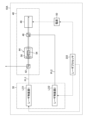
- Embodiment 1 4 shows a schematic configuration of a laser system 10A according to embodiment 1.
- the laser system 10A includes a laser oscillator system 30, a beam combiner 40, and a laser processor 222.
- the laser oscillator system 30 includes a first laser oscillator LO1 and a second laser oscillator LO2. Note that the notation “laser oscillator 1" in the figure represents the first laser oscillator LO1, and the notation “laser oscillator 2" represents the second laser oscillator LO2.
- the first laser oscillator LO1 outputs a first pulsed laser light PL1 with an ultraviolet wavelength of 150 nm to 380 nm and a first polarization direction.
- the first laser oscillator LO1 may be a KrF excimer laser or an ArF excimer laser.
- the spectral linewidth of the first pulsed laser light PL1 may be narrowed to 1 pm or less.
- the second laser oscillator LO2 outputs a second pulsed laser light PL2 having an ultraviolet wavelength of 150 nm to 380 nm and a second polarization direction rotated 45 degrees counterclockwise with respect to the first polarization direction.
- the counterclockwise direction is an example of the "first rotation direction" in this disclosure.
- the second laser oscillator LO2 may be a KrF excimer laser or an ArF excimer laser.
- the spectral linewidth of the second pulsed laser light PL2 may be narrowed to 1 pm or less.
- the laser processor 222 functions as a control device for the laser system 10A.
- the laser processor 222 is a processing device including a storage device in which a control program is stored, and a CPU (Central Processing Unit) that executes the control program.
- the laser processor 222 is specially configured or programmed to execute various processes included in the present disclosure.
- the storage device is a tangible, non-transitory computer-readable medium, and includes, for example, a memory that is a primary storage device and a storage that is an auxiliary storage device.
- the computer-readable medium may be, for example, a semiconductor memory, a hard disk drive (HDD) device, or a solid state drive (SSD) device, or a combination of two or more of these.
- the beam combiner 40 includes a first polarizer 42, a Faraday rotator 44, a second polarizer 46, and a multi-pass Faraday mirror 48.
- the laser system 10A also includes a power supply 50 that supplies current to the multi-pass Faraday mirror 48.
- Each of the first laser oscillator LO1, the second laser oscillator LO2, and the power supply 50 is controlled by the laser processor 222.
- the first polarizer 42 is positioned so that the first pulsed laser light PL1 passes through it.
- the first polarizer 42 may be, for example, a polarizing prism or a thin film polarizer.
- the Faraday rotator 44 is disposed so that the first pulsed laser light PL1 transmitted through the first polarizer 42 passes through it.
- the Faraday rotator 44 is composed of a Faraday material 54 that rotates the polarization direction of the first pulsed laser light PL1 by 45 degrees clockwise when viewed in the direction in which the first pulsed laser light PL1 travels, and a permanent magnet 56.
- the clockwise direction is an example of a "second rotation direction" in this disclosure.
- the Faraday material 54 may be, for example, CaF 2 , MgF 2 , or synthetic quartz.
- the permanent magnet 56 applies a magnetic field to the Faraday material 54.
- the Faraday rotator 44 is an example of a "first Faraday rotator" in this disclosure.
- the Faraday material 54 is an example of a "second Faraday material” in this disclosure
- the permanent magnet 56 is an example of a "first permanent magnet” in this disclosure.
- the second polarizer 46 is arranged so as to transmit the first pulsed laser light PL1 that has passed through the Faraday rotator 44 and to reflect the second pulsed laser light PL2.
- the second polarizer 46 may be, for example, a polarizing prism or a thin-film polarizer.
- the multi-path Faraday mirror 48 is positioned so that the first pulsed laser light PL1 that has passed through the second polarizer 46 is incident on it.
- the configuration diagram of the multi-path Faraday mirror 48 is shown in Figure 5.
- the multi-path Faraday mirror 48 includes a Faraday material 64 that rotates the polarization direction of the pulsed laser light PL by 90 degrees clockwise when viewed in the direction in which the pulsed laser light PL travels, a coil 66 that constitutes an electromagnet, a high-reflection mirror 71, a high-reflection mirror 72, a high-reflection mirror 73, and a high-reflection mirror 74.
- the Faraday material 64 may be, for example, CaF2 , MgF2 , or synthetic quartz.
- the Faraday material 64 is an example of a "first Faraday material" in this disclosure.
- the high-reflection mirrors 71 to 74 are positioned so that the pulsed laser light PL incident on the multi-path Faraday mirror 48 is reflected by high-reflection mirror 71, high-reflection mirror 72, high-reflection mirror 73, and high-reflection mirror 74, and is further reflected by high-reflection mirror 73, high-reflection mirror 72, and high-reflection mirror 71, and is emitted coaxially with the incident pulsed laser light PL.
- FIG. 5 shows an example in which the pulsed laser light PL makes eight passes (passes through the Faraday material 64 eight times), the number of passes may be an even number equal to or greater than four.
- the pulsed laser light PL may be either a first pulsed laser light PL1 or a second pulsed laser light PL2.
- Highly reflective mirrors 71 to 74 are an example of the "multiple reflective mirrors" in this disclosure.
- the power supply 50 is connected to the coil 66.
- a current flows from the power supply 50 to the coil 66, a magnetic field is applied to the Faraday material 64.
- the laser processor 222 causes the laser oscillator system 30 to alternately output the first pulsed laser light PL1 and the second pulsed laser light PL2 at the same repetition rate.
- FIG. 6 shows the propagation of the first pulsed laser light PL1 output from the first laser oscillator LO1.
- the first pulsed laser light PL1 with the first polarization direction output from the first laser oscillator LO1 passes through the first polarizer 42.
- the polarization direction of the first pulsed laser light PL1 rotates 45 degrees clockwise to the third polarization direction.
- the double-headed arrow in the dashed circle in the figure indicates the direction of the polarization plane of the pulsed laser light PL when the line of sight is aligned with the direction in which the pulsed laser light PL travels, i.e., the polarization direction.
- the first pulsed laser light PL1 that passes through the Faraday rotator 44 passes through the second polarizer 46.
- the first pulsed laser light PL1 that passes through the second polarizer 46 enters the multi-pass Faraday mirror 48.
- the first pulsed laser light PL1 incident on the multi-path Faraday mirror 48 passes through the Faraday material 64 eight times before being reflected toward the second polarizer 46.
- the laser processor 222 does not pass current through the coil 66 via the power supply 50.
- the electromagnet is OFF.
- the polarization direction of the first pulsed laser light PL1 does not rotate when it passes through the multi-path Faraday mirror 48. Therefore, the polarization direction of the first pulsed laser light PL1 output from the multi-path Faraday mirror 48 remains the third polarization direction.
- the first pulsed laser light PL1 having the third polarization direction reflected by the multi-path Faraday mirror 48 passes through the second polarizer 46 and has its polarization direction rotated 45 degrees clockwise by the Faraday rotator 44 to become the fourth polarization direction.
- the first pulsed laser light PL1 having the fourth polarization direction is reflected by the first polarizer 42 and output from the laser system 10A.
- FIG. 7 shows the propagation of the second pulsed laser light PL2 output from the second laser oscillator LO2.
- the second pulsed laser light PL2 having the second polarization direction output from the second laser oscillator LO2 is reflected by the second polarizer 46.
- the second pulsed laser light PL2 then enters the multi-path Faraday mirror 48.
- the second pulsed laser light PL2 incident on the multi-pass Faraday mirror 48 passes through the Faraday material 64 eight times before being reflected towards the second polarizer 46.
- the laser processor 222 passes a current through the coil 66 via the power supply 50.
- the electromagnet is ON.
- the strength of the magnetic field generated by the electromagnet ranges from 0.005 T to 1.0 T.
- the polarization direction rotates 90 degrees clockwise. Therefore, the polarization direction of the second pulsed laser light PL2 reflected by the multi-path Faraday mirror 48 becomes the third polarization direction.
- the second pulsed laser light PL2 having the third polarization direction reflected by the multi-path Faraday mirror 48 passes through the second polarizer 46 and has its polarization direction rotated 45 degrees clockwise by the Faraday rotator 44 to become the fourth polarization direction.
- the second pulsed laser light PL2 having the fourth polarization direction is reflected by the first polarizer 42 and output from the laser system 10A.
- the laser processor 222 turns the electromagnet OFF when the first pulsed laser light PL1 is incident on the multi-path Faraday mirror 48, and turns the electromagnet ON when the second pulsed laser light PL2 is incident on the multi-path Faraday mirror 48.
- the first pulsed laser light PL1 with the first polarization direction and the second pulsed laser light PL2 with the second polarization direction output from the laser oscillator system 30 are combined in the beam combiner 40 so as to propagate in a common direction.
- the combined first pulsed laser light PL1 and second pulsed laser light PL2 in the fourth polarization direction are alternately output from the laser system 10A.
- the beam combiner 40 also functions when the clockwise and counterclockwise directions in the above embodiment are reversed. However, in this case, the polarization direction of the light passing through the second polarizer 46 differs by 90 degrees from that described above.
- the beam combiner 40 does not have any moving parts such as the actuator 210 shown in Figures 2 and 3, so the position repeatability of the pulsed laser light PL (the first pulsed laser light PL1 and the second pulsed laser light PL2) output from the laser system 10A is high.
- the electromagnet By making the pulsed laser light pass multiple times in the multi-path Faraday mirror 48, the electromagnet can be made smaller and the current passed through the coil 66 can be reduced.
- Pulsed laser light PL with the same polarization direction can be output from the laser system 10A.
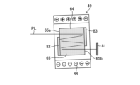
- FIG. 8 shows the configuration of a multi-path Faraday mirror 49 according to a modification of embodiment 1.
- the multi-path Faraday mirror 49 shown in FIG. 8 can be used.
- the multipath Faraday mirror 49 includes a Faraday material 65, a high-reflection mirror 81, and a coil 66 that constitutes an electromagnet.
- the Faraday material 65 has high-reflection coatings 82, 83 applied to a portion of each of a first surface 65a, which is the surface on which the pulsed laser light PL is incident, and a second surface 65b, which is the surface from which the pulsed laser light PL is output toward the high-reflection mirror 81.
- the pulsed laser light PL incident on the multi-path Faraday mirror 49 enters the Faraday material 65 from a portion of the first surface 65a that is not provided with the high-reflection coating 82.
- the pulsed laser light PL is then reflected by the high-reflection coating 83 and the high-reflection coating 82, and is output from a portion of the second surface 65b that is not provided with the high-reflection coating 83.
- the pulsed laser light PL output from the second surface 65b of the Faraday material 65 is reflected by the high-reflection mirror 81 and then returns to the Faraday material 65.
- the pulsed laser light PL reflected by the high-reflection mirror 81 enters the Faraday material 65 from a portion of the second surface 65b where the high-reflection coating 83 is not applied, is reflected by the high-reflection coating 82 and the high-reflection coating 83, and is then output from a portion of the first surface 65a where the high-reflection coating 82 is not applied. It is preferable that the high-reflection coating 82 and the high-reflection coating 83 are each reflected two or more times. In other words, it is desirable that the pulsed laser light PL makes four or more passes through the Faraday material 65.
- the high-reflection mirror 81 and the high-reflection coatings 82 and 83 are examples of "multiple reflecting mirrors" in this disclosure.
- the laser processor 222 passes a current through the coil 66 via the power supply 50, that is, when the electromagnet is ON, the polarization direction of the pulsed laser light PL rotates 90 degrees clockwise when it passes through the multi-path Faraday mirror 49.
- the laser processor 222 controls the current (electromagnet current) passed through the coil 66 via the power supply 50 to switch the electromagnet ON/OFF, in the same manner as in embodiment 1.
- the laser system 10A equipped with the multi-path Faraday mirror 49 according to the modified example can provide the same effects as those of the embodiment 1.
- the multi-path Faraday mirror 49 according to the modified example can reduce the number of high-reflection mirrors compared to the multi-path Faraday mirror 48 of the embodiment 1, and the position repeatability and the like are further improved compared to the embodiment 1.
- Embodiment 2 4.1 Configuration Fig. 9 shows a schematic configuration of a laser system 10B according to the second embodiment.
- the laser system 10B will be described with respect to differences from the laser system 10A shown in Fig. 4.
- the laser system 10B includes a laser oscillator system 32 instead of the laser oscillator system 30 shown in Fig. 4.
- the laser oscillator system 32 includes a third laser oscillator LO3 instead of the second laser oscillator LO2 shown in Fig. 4, and a Faraday rotator 90. Note that the notation "laser oscillator 3" in the figure refers to the third laser oscillator LO3.
- the third laser oscillator LO3 outputs a second pulsed laser light PL2 having an ultraviolet wavelength of 150 nm to 380 nm in a first polarization direction.
- the third laser oscillator LO3 may be a KrF excimer laser or an ArF excimer laser.
- the spectral linewidth of the second pulsed laser light PL2 output from the third laser oscillator LO3 may be narrowed to 1 pm or less.
- the Faraday rotator 90 is composed of a Faraday material 94 that rotates the polarization direction of the second pulsed laser light PL2 by 45 degrees counterclockwise when viewed in the direction in which the second pulsed laser light PL2 travels, and a permanent magnet 96.
- the Faraday material 94 may be, for example, CaF2 , MgF2 , or synthetic quartz.
- a wave plate that rotates the polarization direction of the second pulsed laser light PL2 by 45 degrees counterclockwise may be used.
- the other configurations are the same as those shown in FIG. 4.
- Faraday rotator 90 is an example of a "second Faraday rotator" in this disclosure.
- Faraday material 94 is an example of a “third Faraday material” in this disclosure, and permanent magnet 96 is an example of a "second permanent magnet” in this disclosure.
- the laser processor 222 alternately outputs the first pulsed laser beam PL1 and the second pulsed laser beam PL2 at the same repetition rate.
- Fig. 10 shows the propagation of the second pulsed laser beam PL2 output from the third laser oscillator LO3.
- the second pulsed laser light PL2 output from the third laser oscillator LO3 passes through the Faraday rotator 90. At this time, the polarization direction of the second pulsed laser light PL2 rotates 45 degrees counterclockwise to become the second polarization direction.
- the second pulsed laser light PL2 that passes through the Faraday rotator 90 is reflected by the second polarizer 46 and enters the multi-path Faraday mirror 48. Subsequent propagation is the same as in embodiment 1.
- the propagation of the first pulsed laser light PL1 output from the first laser oscillator LO1 is the same as in embodiment 1, and the control of the current flowing through the electromagnet via the power supply 50 and other operations are also the same as in embodiment 1.
- the laser system 10B according to the embodiment 2 can provide the same effects as those of the embodiment 1.
- the polarization directions of the first pulsed laser beam PL1 output from the first laser oscillator LO1 and the second pulsed laser beam PL2 output from the third laser oscillator LO3 can be made the same.
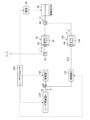
- FIG. 11 shows the configuration of a laser system 10C according to the third embodiment.
- the laser system 10C will be described with respect to differences from the laser system 10A shown in FIG. 4.
- the laser system 10C includes a laser oscillator system 33 instead of the laser oscillator system 30 shown in FIG. 4.
- the laser oscillator system 33 includes a fourth laser oscillator LO4, a beam splitter BS, a first amplifier 130, a second amplifier 132, and a Faraday rotator 140.
- the notation “laser oscillator 4" in the figure represents the fourth laser oscillator LO4.
- the notations "amplifier 1" and “amplifier 2" in the figure represent the first amplifier 130 and the second amplifier 132.
- the fourth laser oscillator LO4 outputs seed light SL in the first polarization direction with an ultraviolet wavelength of 150 nm to 380 nm.
- the fourth laser oscillator LO4 may be a solid-state laser capable of high repetition rate operation and outputting seed light SL with the wavelength of a KrF laser or an ArF laser.
- the spectral line width of the seed light SL output from the fourth laser oscillator LO4 may be narrowed to 1 pm or less.
- the solid-state laser may be, for example, a triple wave (wavelength 248.4 nm) of a Ti sapphire laser with a wavelength of 745.2 nm, or a quadruple wave (wavelength 193.4 nm) of a Ti sapphire laser with a wavelength of 773.6 nm.
- the beam splitter BS splits the seed beam SL output from the fourth laser oscillator LO4 into two seed beams SL.
- the split ratio of the transmitted light amount to the reflected light amount in the beam splitter BS may be 1:1.
- the first amplifier 130 and the second amplifier 132 each amplify the seed light SL separated by the beam splitter BS.
- the first amplifier 130 and the second amplifier 132 are, for example, discharge-pumped excimer amplifiers, and may include a Fabry-Perot resonator, a ring resonator, or a multi-pass amplifier.
- a multi-pass amplifier is configured to reflect a beam that has passed through the amplifier using multiple reflecting mirrors, causing the beam to pass through the same amplifier multiple times.
- the repetition frequency of the first amplifier 130 and the second amplifier 132 is the same, and the repetition frequency of the fourth laser oscillator LO4 is twice the repetition frequency of the first amplifier 130 and the second amplifier 132.
- the repetition frequency of each of the first amplifier 130 and the second amplifier 132 is 6 kHz, and the repetition frequency of the fourth laser oscillator LO4 is 12 kHz.
- the Faraday rotator 140 is composed of a Faraday material 144 that rotates the polarization direction of the pulsed laser light PL by 45 degrees counterclockwise when viewed in the direction in which the pulsed laser light PL travels, and a permanent magnet 146.
- the Faraday material 144 may be, for example, CaF2 , MgF2 , or synthetic quartz.
- a wave plate that rotates the polarization direction of the pulsed laser light PL by 45 degrees counterclockwise may be used.
- the other configurations are the same as those in FIG. 4.
- Faraday rotator 140 is an example of a "third Faraday rotator" in this disclosure.
- Faraday material 144 is an example of a “fourth Faraday material” in this disclosure, and permanent magnet 146 is an example of a "third permanent magnet” in this disclosure.
- the laser processor 222 alternately operates the first amplifier 130 and the second amplifier 132 for each pulse of the seed light SL.
- the first amplifier 130 When the first amplifier 130 operates, it amplifies one of the seed lights SL separated by the beam splitter BS and outputs the first pulsed laser light PL1.
- the second amplifier 132 When the second amplifier 132 operates, the second amplifier 132 amplifies the other seed light SL split by the beam splitter BS and outputs the second pulsed laser light PL2.
- FIG. 12 shows the propagation of the first pulsed laser light PL1 output from the first amplifier 130.
- the propagation of the first pulsed laser light PL1 output from the first amplifier 130 is similar to that in embodiment 1.
- FIG. 13 shows the propagation of the second pulsed laser light PL2 output from the second amplifier 132.
- the propagation of the second pulsed laser light PL2 output from the second amplifier 132 is similar to that in the second embodiment.
- the laser processor 222 turns the electromagnet OFF when the first pulsed laser light PL1 is incident on the multi-path Faraday mirror 48, and turns the electromagnet ON when the second pulsed laser light PL2 is incident on the multi-path Faraday mirror 48.
- the first pulsed laser light PL1 in the first polarization direction and the second pulsed laser light PL2 in the second polarization direction are combined by the beam combiner 40 so as to propagate in a common direction.
- the combined first pulsed laser light PL1 and second pulsed laser light PL2 in the fourth polarization direction are alternately output from the laser system 10C.
- the laser system 10C according to the third embodiment can provide the same effects as those of the first embodiment. Since the laser system 10C includes only one fourth laser oscillator LO4, it is possible to reduce fluctuations in the wavelength and the spectral linewidth of the pulsed laser light output from the laser system 10C.
- FIG. 14 shows a schematic configuration of an exposure apparatus 800.
- the exposure apparatus 800 includes an illumination optical system 806 and a projection optical system 808.
- the laser system 10A generates a laser beam and outputs the laser beam to the exposure apparatus 800.
- the illumination optical system 806 illuminates a reticle pattern of a reticle (not shown) arranged on a reticle stage RT with the laser beam incident from the laser system 10A.
- the projection optical system 808 reduces and projects the laser beam transmitted through the reticle to form an image on a workpiece (not shown) arranged on a workpiece table WT.
- the workpiece is a photosensitive substrate such as a semiconductor wafer coated with photoresist.
- the exposure apparatus 800 exposes the workpiece to laser light reflecting the reticle pattern by synchronously translating the reticle stage RT and the workpiece table WT. After the reticle pattern is transferred to the semiconductor wafer by the exposure process described above, a semiconductor device can be manufactured through multiple processes.
- a semiconductor device is an example of an "electronic device" in this disclosure. The configuration is not limited to using laser system 10A, and laser systems 10B, 10C, etc. may also be used.
Landscapes
- Physics & Mathematics (AREA)
- Electromagnetism (AREA)
- Engineering & Computer Science (AREA)
- Plasma & Fusion (AREA)
- Optics & Photonics (AREA)
- General Physics & Mathematics (AREA)
- Nonlinear Science (AREA)
- Power Engineering (AREA)
- Lasers (AREA)
Abstract
Description
1.用語の説明
1.1 ファラデー材料
1.2 マルチパスファラデーミラー
2.比較例に係るレーザシステムの概要
2.1 構成
2.2 動作
2.3 課題
3.実施形態1
3.1 構成
3.2 動作
3.3 効果
3.4 変形例
3.4.1 構成
3.4.2 動作
3.4.3 効果
4.実施形態2
4.1 構成
4.2 動作
4.3 効果
5.実施形態3
5.1 構成
5.2 動作
5.3 効果
6.電子デバイスの製造方法について
7.その他
以下、本開示の実施形態について、図面を参照しながら詳しく説明する。以下に説明される実施形態は、本開示のいくつかの例を示すものであって、本開示の内容を限定するものではない。また、各実施形態で説明される構成及び動作の全てが本開示の構成及び動作として必須であるとは限らない。なお、同一の構成要素には同一の参照符号を付して、重複する説明を省略する。
1.1 ファラデー材料
ファラデー材料とは、外部から磁場を印加することで磁気光学効果のファラデー効果が起こる材料をいう。どの材料でもファラデー効果は起こるが、本明細書では、波長が150nmから380nmの紫外線波長においてファラデー効果が得られる材料のことを指す。深紫外領域においては、ファラデー材料の候補材料として、フッ化カルシウム(CaF2)、フッ化マグネシウム(MgF2)、合成石英等がある。
マルチパスファラデーミラーは、ファラデー材料と、ファラデー材料に磁場を印加する電磁石と、ファラデー材料を透過した光をファラデー材料に折り返す複数の反射ミラーとで構成される。複数の反射ミラーは、マルチパスファラデーミラーに入射する光の光軸とマルチパスファラデーミラーから出力される光の光軸とが同じになるように配置される。
2.1 構成
図1は、比較例に係るレーザシステム10の構成を概略的に示す構成図である。本開示の比較例とは、出願人のみによって知られていると出願人が認識している形態であって、出願人が自認している公知例ではない。レーザシステム10は、第1のレーザ発振器LO1と、第2のレーザ発振器LO2と、ビームコンバイナ20と、レーザプロセッサ220と、を含む。
第1のレーザ発振器LO1から出力された第1のパルスレーザ光100をレーザシステム10から出力するときは、ビームコンバイナ20のミラー200の位置が図2の実線で示す第1の位置になるようにレーザプロセッサ220からアクチュエータ210へ制御信号を送信する。第2のレーザ発振器LO2から出力された第2のパルスレーザ光120をレーザシステム10から出力するときは、ビームコンバイナ20のミラー200の位置が図3の実線で示す第2の位置になるようにレーザプロセッサ220からアクチュエータ210へ制御信号を送信する。
上記のビームコンバイナ20はアクチュエータ210でミラー200の位置を切り替える可動部を含むが、12kHz等の高繰返し周波数の周期で再現性よく位置を切り替えることは困難である。このため、レーザシステム10から出力されるパルスレーザ光の位置再現性が悪い。
3.1 構成
図4は、実施形態1に係るレーザシステム10Aの構成を概略的に示す。レーザシステム10Aは、レーザ発振器システム30と、ビームコンバイナ40と、レーザプロセッサ222と、を備える。
レーザプロセッサ222は、レーザ発振器システム30から第1のパルスレーザ光PL1と第2のパルスレーザ光PL2とを、同じ繰返し周波数で交互に出力させる。
実施形態1に係るレーザシステム10Aによれば、次の効果が得られる。
3.4.1 構成
図8に、実施形態1の変形例に係るマルチパスファラデーミラー49の構成を示す。図5に示したマルチパスファラデーミラー48の代わりに、図8に示すマルチパスファラデーミラー49を用いることができる。
マルチパスファラデーミラー49に入射したパルスレーザ光PLは、第1の面65aの高反射コート82が施されていない部分からファラデー材料65に入射する。そして、パルスレーザ光PLは、高反射コート83と高反射コート82とで反射された後、第2の面65bの高反射コート83が施されていない部分から出力される。
変形例に係るマルチパスファラデーミラー49を備えたレーザシステム10Aによれば、実施形態1と同じ効果が得られる。変形例に係るマルチパスファラデーミラー49は実施形態1のマルチパスファラデーミラー48よりも高反射ミラーの枚数を減らすことができ、実施形態1よりも位置再現性などが一層向上する。
4.1 構成
図9は、実施形態2に係るレーザシステム10Bの構成を概略的に示す。レーザシステム10Bについて、図4に示すレーザシステム10Aと異なる点を説明する。レーザシステム10Bは、図4に示すレーザ発振器システム30の代わりにレーザ発振器システム32を備える。レーザ発振器システム32は、図4に示す第2のレーザ発振器LO2の代わりに第3のレーザ発振器LO3と、ファラデー回転子90と、を備える。なお、図中の「レーザ発振器3」の表記は第3のレーザ発振器LO3を表す。
レーザプロセッサ222は、第1のパルスレーザ光PL1と第2のパルスレーザ光PL2とを、同じ繰返し周波数で交互に出力させる。図10は、第3のレーザ発振器LO3から出力された第2のパルスレーザ光PL2の伝搬の様子を示す。
実施形態2に係るレーザシステム10Bよれば、実施形態1と同じ効果が得られる。レーザシステム10Bでは、第1のレーザ発振器LO1から出力される第1のパルスレーザ光PL1と第3のレーザ発振器LO3から出力される第2のパルスレーザ光PL2の偏光方向を同じにすることができる。
5.1 構成
図11は、実施形態3に係るレーザシステム10Cの構成を示す。レーザシステム10Cについて、図4に示すレーザシステム10Aと異なる点を説明する。レーザシステム10Cは、図4に示すレーザ発振器システム30の代わりにレーザ発振器システム33を備える。レーザ発振器システム33は、第4のレーザ発振器LO4と、ビームスプリッタBSと、第1の増幅器130と、第2の増幅器132と、ファラデー回転子140と、を備える。なお、図中の「レーザ発振器4」の表記は第4のレーザ発振器LO4を表す。また、図中の「増幅器1」及び「増幅器2」の表記は第1の増幅器130及び第2の増幅器132を表す。
第4のレーザ発振器LO4から出力された第1の偏光方向のシード光SLは、ビームスプリッタBSで50%が透過して第1の増幅器130に入射し、他の50%が反射して第2の増幅器132に入射する。
実施形態3に係るレーザシステム10Cよれば、実施形態1と同じ効果が得られる。レーザシステム10Cでは、第4のレーザ発振器LO4が1つであるので、レーザシステム10Cから出力されるパルスレーザ光の波長やスペクトル線幅の変動を小さくできる。
図14は、露光装置800の構成を概略的に示す。露光装置800は、照明光学系806と投影光学系808とを含む。レーザシステム10Aはレーザ光を生成し、レーザ光を露光装置800に出力する。照明光学系806は、レーザシステム10Aから入射したレーザ光によって、レチクルステージRT上に配置された不図示のレチクルのレチクルパターンを照明する。投影光学系808は、レチクルを透過したレーザ光を、縮小投影してワークピーステーブルWT上に配置された不図示のワークピースに結像させる。ワークピースはフォトレジストが塗布された半導体ウエハ等の感光基板である。
上記の説明は、制限ではなく単なる例示を意図している。したがって、特許請求の範囲を逸脱することなく本開示の実施形態に変更を加えることができることは、当業者には明らかである。また、本開示の実施形態を組み合わせて使用することも当業者には明らかである。
Claims (17)
- 第1の偏光方向の第1のパルスレーザ光と前記第1の偏光方向に対して第1の回転方向に45度回転した第2の偏光方向の第2のパルスレーザ光とを出力するレーザ発振器システムと、
前記第1のパルスレーザ光と前記第2のパルスレーザ光とを共通の方向に伝搬させるように前記第1のパルスレーザ光と前記第2のパルスレーザ光とを結合するビームコンバイナであって、
前記第1のパルスレーザ光を透過する第1の偏光子と、
前記第1の偏光子を透過した前記第1のパルスレーザ光の偏光方向を前記第1の回転方向に対して逆方向の第2の回転方向に45度回転させる第1のファラデー回転子と、
前記第1のファラデー回転子を透過した前記第1のパルスレーザ光を透過し、前記第2のパルスレーザ光を反射する第2の偏光子と、
前記第2の偏光子を透過した前記第1のパルスレーザ光と前記第2の偏光子で反射された前記第2のパルスレーザ光とを前記第2の偏光子に向けて反射するマルチパスファラデーミラーと、を備え、
前記マルチパスファラデーミラーは、前記第1のパルスレーザ光及び前記第2のパルスレーザ光が透過する第1のファラデー材料と、前記第1のファラデー材料に磁場を印加する電磁石と、前記第1のファラデー材料を透過した前記第1のパルスレーザ光及び前記第2のパルスレーザ光を前記第1のファラデー材料に折り返す複数の反射ミラーと、
を備える前記ビームコンバイナと、
前記電磁石に電流を流す電源と、
前記第1のパルスレーザ光が前記第1のファラデー材料を透過するときに前記電磁石に電流を流さず、前記第2のパルスレーザ光が前記第1のファラデー材料を透過するときに前記第2のパルスレーザ光の偏光方向を90度回転させる電流を前記電磁石に流すように、前記電源を介して前記電磁石に流れる電流を制御するプロセッサと、
を備えるレーザシステム。 - 請求項1に記載のレーザシステムであって、
前記プロセッサは、前記レーザ発振器システムから前記第1のパルスレーザ光と前記第2のパルスレーザ光とを交互に出力させる、
レーザシステム。 - 請求項1に記載のレーザシステムであって、
前記第1のファラデー材料は、フッ化カルシウム、フッ化マグネシウム又は合成石英である、
レーザシステム。 - 請求項1に記載のレーザシステムであって、
前記第1のファラデー回転子は、第2のファラデー材料と、前記第2のファラデー材料に磁場を印加する第1の永久磁石と、を含み、
前記第2のファラデー材料は、フッ化カルシウム、フッ化マグネシウム又は合成石英である、
レーザシステム。 - 請求項1に記載のレーザシステムであって、
前記マルチパスファラデーミラーは、入射した前記第1のパルスレーザ光と前記第2のパルスレーザ光とが前記第1のファラデー材料を8回通過してから前記第2の偏光子に向けて出射されるように、前記第1のファラデー材料を透過した前記第1のパルスレーザ光と前記第2のパルスレーザ光を反射する前記複数の反射ミラーである4つの高反射ミラーを含む、
レーザシステム。 - 請求項1に記載のレーザシステムであって、
前記第1のファラデー材料は、入射した前記第1のパルスレーザ光と前記第2のパルスレーザ光とが前記第1のファラデー材料を複数回通過して前記第2の偏光子に向けて出力されるように、前記第1のファラデー材料における前記第1のパルスレーザ光と前記第2のパルスレーザ光とが入射する面及び前記第1のパルスレーザ光と前記第2のパルスレーザ光とが出力される面のそれぞれの一部に、前記第1のパルスレーザ光と前記第2のパルスレーザ光とを反射する前記複数の反射ミラーとしての反射コートを含む、
レーザシステム。 - 請求項1に記載のレーザシステムであって、
前記レーザ発振器システムは、前記第1の偏光方向の前記第1のパルスレーザ光を出力する第1のレーザ発振器と、
前記第2の偏光方向の前記第2のパルスレーザ光を出力する第2のレーザ発振器と、を備える、
レーザシステム。 - 請求項1に記載のレーザシステムであって、
前記レーザ発振器システムは、前記第1の偏光方向の前記第1のパルスレーザ光を出力する第1のレーザ発振器と、
前記第1の偏光方向の前記第2のパルスレーザ光を出力する第3のレーザ発振器と、
前記第3のレーザ発振器から出力された前記第1のパルスレーザ光の偏光方向を前記第1の回転方向に45度回転させる第2のファラデー回転子と、を備え、
前記第2のファラデー回転子から前記第2の偏光方向の前記第2のパルスレーザ光を出力させる、
レーザシステム。 - 請求項8に記載のレーザシステムであって、
前記第2のファラデー回転子は、第3のファラデー材料と前記第3のファラデー材料に磁場を印加する第2の永久磁石とを含み、
前記第3のファラデー材料は、フッ化カルシウム、フッ化マグネシウム又は合成石英である、
レーザシステム。 - 請求項1に記載のレーザシステムであって、
前記レーザ発振器システムは、
前記第1の偏光方向のシード光を出力する第4のレーザ発振器と、
前記シード光を分離するビームスプリッタと、
前記ビームスプリッタで分離された一方のシード光を増幅し前記第1のパルスレーザ光を出力する第1の増幅器と、
前記ビームスプリッタで分離された他方のシード光を増幅し前記第2のパルスレーザ光を出力する第2の増幅器と、
前記第2の増幅器から出力された前記第2のパルスレーザ光の偏光方向を前記第1の回転方向に45度回転させる第3のファラデー回転子と、を備える、
レーザシステム。 - 請求項10に記載のレーザシステムであって、
前記第3のファラデー回転子は、第4のファラデー材料と前記第4のファラデー材料に磁場を印加する第3の永久磁石とを含み、
前記第4のファラデー材料は、フッ化カルシウム、フッ化マグネシウム又は合成石英である、
レーザシステム。 - 請求項10に記載のレーザシステムであって、
前記第4のレーザ発振器は、KrFエキシマレーザ又はArFエキシマレーザの波長の前記シード光を出力する固体レーザである、
レーザシステム。 - 請求項10に記載のレーザシステムであって、
前記第1の増幅器と前記第2の増幅器とのそれぞれは、ファブリーペロー共振器、リング共振器又はマルチパス増幅器を含む、
レーザシステム。 - 請求項10に記載のレーザシステムであって、
前記プロセッサは、前記第4のレーザ発振器から出力される前記シード光のパルス毎に、前記第1の増幅器と前記第2の増幅器とを交互に動作させる、
レーザシステム。 - 請求項1に記載のレーザシステムであって、
前記第1のパルスレーザ光と前記第2のパルスレーザ光との波長は紫外線波長である、
レーザシステム。 - 請求項1に記載のレーザシステムであって、
前記ビームコンバイナによって結合されて出力される前記第1のパルスレーザ光と前記第2のパルスレーザ光とは同じ偏光方向である、
レーザシステム。 - 電子デバイスの製造方法であって、
第1の偏光方向の第1のパルスレーザ光と前記第1の偏光方向に対して第1の回転方向に45度回転した第2の偏光方向の第2のパルスレーザ光とを出力するレーザ発振器システムと、
前記第1のパルスレーザ光と前記第2のパルスレーザ光とを共通の方向に伝搬させるように前記第1のパルスレーザ光と前記第2のパルスレーザ光とを結合するビームコンバイナであって、
前記第1のパルスレーザ光を透過する第1の偏光子と、
前記第1の偏光子を透過した前記第1のパルスレーザ光の偏光方向を前記第1の回転方向に対して逆方向の第2の回転方向に45度回転させる第1のファラデー回転子と、
前記第1のファラデー回転子を透過した前記第1のパルスレーザ光を透過し、前記第2のパルスレーザ光を反射する第2の偏光子と、
前記第2の偏光子を透過した前記第1のパルスレーザ光と前記第2の偏光子で反射された前記第2のパルスレーザ光とを前記第2の偏光子に向けて反射するマルチパスファラデーミラーと、を備え、
前記マルチパスファラデーミラーは、前記第1のパルスレーザ光及び前記第2のパルスレーザ光が透過する第1のファラデー材料と、前記第1のファラデー材料に磁場を印加する電磁石と、前記第1のファラデー材料を透過した前記第1のパルスレーザ光及び前記第2のパルスレーザ光を前記第1のファラデー材料に折り返す複数の反射ミラーと、
を備える前記ビームコンバイナと、
前記電磁石に電流を流す電源と、
前記第1のパルスレーザ光が前記第1のファラデー材料を透過するときに前記電磁石に電流を流さず、前記第2のパルスレーザ光が前記第1のファラデー材料を透過するときに前記第2のパルスレーザ光の偏光方向を90度回転させる電流を前記電磁石に流すように、前記電源を介して前記電磁石に流れる電流を制御するプロセッサと、
を備えるレーザシステムによってレーザ光を生成し、
前記レーザ光を露光装置に出力し、
電子デバイスを製造するために、前記露光装置内で感光基板に前記レーザ光を露光することを含む、
電子デバイスの製造方法。
Priority Applications (4)
| Application Number | Priority Date | Filing Date | Title |
|---|---|---|---|
| CN202380093072.2A CN120677600A (zh) | 2023-03-28 | 2023-03-28 | 激光系统及电子器件的制造方法 |
| PCT/JP2023/012679 WO2024201755A1 (ja) | 2023-03-28 | 2023-03-28 | レーザシステム及び電子デバイスの製造方法 |
| JP2025509372A JPWO2024201755A1 (ja) | 2023-03-28 | 2023-03-28 | |
| US19/289,812 US20250357721A1 (en) | 2023-03-28 | 2025-08-04 | Laser system and electronic device manufacturing method |
Applications Claiming Priority (1)
| Application Number | Priority Date | Filing Date | Title |
|---|---|---|---|
| PCT/JP2023/012679 WO2024201755A1 (ja) | 2023-03-28 | 2023-03-28 | レーザシステム及び電子デバイスの製造方法 |
Related Child Applications (1)
| Application Number | Title | Priority Date | Filing Date |
|---|---|---|---|
| US19/289,812 Continuation US20250357721A1 (en) | 2023-03-28 | 2025-08-04 | Laser system and electronic device manufacturing method |
Publications (1)
| Publication Number | Publication Date |
|---|---|
| WO2024201755A1 true WO2024201755A1 (ja) | 2024-10-03 |
Family
ID=92903575
Family Applications (1)
| Application Number | Title | Priority Date | Filing Date |
|---|---|---|---|
| PCT/JP2023/012679 Ceased WO2024201755A1 (ja) | 2023-03-28 | 2023-03-28 | レーザシステム及び電子デバイスの製造方法 |
Country Status (4)
| Country | Link |
|---|---|
| US (1) | US20250357721A1 (ja) |
| JP (1) | JPWO2024201755A1 (ja) |
| CN (1) | CN120677600A (ja) |
| WO (1) | WO2024201755A1 (ja) |
Citations (2)
| Publication number | Priority date | Publication date | Assignee | Title |
|---|---|---|---|---|
| JP2013218286A (ja) * | 2012-03-14 | 2013-10-24 | Gigaphoton Inc | ファラデーローテータ、光アイソレータ、レーザ装置、および極端紫外光生成装置 |
| JP2017032851A (ja) * | 2015-08-04 | 2017-02-09 | 株式会社フジクラ | 偏波合成モジュール、これを用いたレーザ装置、及び、偏波合成モジュールの製造方法 |
-
2023
- 2023-03-28 CN CN202380093072.2A patent/CN120677600A/zh active Pending
- 2023-03-28 WO PCT/JP2023/012679 patent/WO2024201755A1/ja not_active Ceased
- 2023-03-28 JP JP2025509372A patent/JPWO2024201755A1/ja active Pending
-
2025
- 2025-08-04 US US19/289,812 patent/US20250357721A1/en active Pending
Patent Citations (2)
| Publication number | Priority date | Publication date | Assignee | Title |
|---|---|---|---|---|
| JP2013218286A (ja) * | 2012-03-14 | 2013-10-24 | Gigaphoton Inc | ファラデーローテータ、光アイソレータ、レーザ装置、および極端紫外光生成装置 |
| JP2017032851A (ja) * | 2015-08-04 | 2017-02-09 | 株式会社フジクラ | 偏波合成モジュール、これを用いたレーザ装置、及び、偏波合成モジュールの製造方法 |
Also Published As
| Publication number | Publication date |
|---|---|
| CN120677600A (zh) | 2025-09-19 |
| US20250357721A1 (en) | 2025-11-20 |
| JPWO2024201755A1 (ja) | 2024-10-03 |
Similar Documents
| Publication | Publication Date | Title |
|---|---|---|
| KR100783669B1 (ko) | 바이어스에 의해 유도된 레티클 회절을 제거한 광학 축소시스템 | |
| JP7193808B2 (ja) | 波長変換システム | |
| CN114902143B (zh) | 脉冲宽度扩展装置和电子器件的制造方法 | |
| US20230375847A1 (en) | Optical isolator, ultraviolet laser device, and electronic device manufacturing method | |
| US12542412B2 (en) | Gas laser device and electronic device manufacturing method | |
| US20240103305A1 (en) | Optical isolator, ultraviolet laser apparatus, and electronic device manufacturing method | |
| JP2026009870A (ja) | 特にマイクロリソグラフィ用の、光学構成要素および光学系 | |
| WO2024201755A1 (ja) | レーザシステム及び電子デバイスの製造方法 | |
| JP2025041919A (ja) | 紫外線レーザ装置、電子デバイスの製造方法、及びシステム | |
| US20240235149A1 (en) | Laser apparatus and electronic device manufacturing method | |
| JP7537690B2 (ja) | 光アイソレータ、紫外線レーザ装置及び電子デバイスの製造方法 | |
| US11837839B2 (en) | Optical pulse stretcher, laser device, and electronic device manufacturing method | |
| US11870209B2 (en) | Laser system and electronic device manufacturing method | |
| JP7726999B2 (ja) | 紫外線レーザ装置及び電子デバイスの製造方法 | |
| JP6140290B2 (ja) | マイクロリソグラフィー投影露光装置用光学システム及びマイクロリソグラフィー露光方法 | |
| JP7782814B2 (ja) | 光学パルスストレッチャ、レーザ装置及び電子デバイスの製造方法 | |
| US20240248410A1 (en) | Euv illumination device and method for operating a microlithographic projection exposure apparatus designed for operation in the euv | |
| US20240255856A1 (en) | Optical component group, in particular for use in an illumination device of a microlithographic projection exposure apparatus | |
| JP2025093721A (ja) | レーザ加工システム、レーザ加工方法、及び電子デバイスの製造方法 | |
| CN121713342A (zh) | 激光装置以及电子器件的制造方法 | |
| JP2024513761A (ja) | レーザシステム | |
| CN113169507A (zh) | 激光系统和电子器件的制造方法 | |
| JPS62243329A (ja) | 光学装置 | |
| JPH01245520A (ja) | パターン転写装置 |
Legal Events
| Date | Code | Title | Description |
|---|---|---|---|
| 121 | Ep: the epo has been informed by wipo that ep was designated in this application |
Ref document number: 23930395 Country of ref document: EP Kind code of ref document: A1 |
|
| ENP | Entry into the national phase |
Ref document number: 2025509372 Country of ref document: JP Kind code of ref document: A |
|
| WWE | Wipo information: entry into national phase |
Ref document number: 2025509372 Country of ref document: JP Ref document number: 202380093072.2 Country of ref document: CN |
|
| WWP | Wipo information: published in national office |
Ref document number: 202380093072.2 Country of ref document: CN |
|
| NENP | Non-entry into the national phase |
Ref country code: DE |
|
| 122 | Ep: pct application non-entry in european phase |
Ref document number: 23930395 Country of ref document: EP Kind code of ref document: A1 |