WO2024201722A1 - イオンミリング装置、メンテナンス方法及びイオンミリング装置の収束電極 - Google Patents
イオンミリング装置、メンテナンス方法及びイオンミリング装置の収束電極 Download PDFInfo
- Publication number
- WO2024201722A1 WO2024201722A1 PCT/JP2023/012549 JP2023012549W WO2024201722A1 WO 2024201722 A1 WO2024201722 A1 WO 2024201722A1 JP 2023012549 W JP2023012549 W JP 2023012549W WO 2024201722 A1 WO2024201722 A1 WO 2024201722A1
- Authority
- WO
- WIPO (PCT)
- Prior art keywords
- electrode
- ion
- focusing
- cathode
- ion source
- Prior art date
- Legal status (The legal status is an assumption and is not a legal conclusion. Google has not performed a legal analysis and makes no representation as to the accuracy of the status listed.)
- Ceased
Links
Images






Classifications
-
- H—ELECTRICITY
- H01—ELECTRIC ELEMENTS
- H01J—ELECTRIC DISCHARGE TUBES OR DISCHARGE LAMPS
- H01J37/00—Discharge tubes with provision for introducing objects or material to be exposed to the discharge, e.g. for the purpose of examination or processing thereof
- H01J37/30—Electron-beam or ion-beam tubes for localised treatment of objects
- H01J37/305—Electron-beam or ion-beam tubes for localised treatment of objects for casting, melting, evaporating, or etching
- H01J37/3053—Electron-beam or ion-beam tubes for localised treatment of objects for casting, melting, evaporating, or etching for evaporating or etching
- H01J37/3056—Electron-beam or ion-beam tubes for localised treatment of objects for casting, melting, evaporating, or etching for evaporating or etching for microworking, e. g. etching of gratings or trimming of electrical components
-
- H—ELECTRICITY
- H01—ELECTRIC ELEMENTS
- H01J—ELECTRIC DISCHARGE TUBES OR DISCHARGE LAMPS
- H01J27/00—Ion beam tubes
- H01J27/02—Ion sources; Ion guns
- H01J27/04—Ion sources; Ion guns using reflex discharge, e.g. Penning ion sources
-
- H—ELECTRICITY
- H01—ELECTRIC ELEMENTS
- H01J—ELECTRIC DISCHARGE TUBES OR DISCHARGE LAMPS
- H01J37/00—Discharge tubes with provision for introducing objects or material to be exposed to the discharge, e.g. for the purpose of examination or processing thereof
- H01J37/02—Details
- H01J37/04—Arrangements of electrodes and associated parts for generating or controlling the discharge, e.g. electron-optical arrangement or ion-optical arrangement
- H01J37/08—Ion sources; Ion guns
-
- H—ELECTRICITY
- H01—ELECTRIC ELEMENTS
- H01J—ELECTRIC DISCHARGE TUBES OR DISCHARGE LAMPS
- H01J37/00—Discharge tubes with provision for introducing objects or material to be exposed to the discharge, e.g. for the purpose of examination or processing thereof
- H01J37/30—Electron-beam or ion-beam tubes for localised treatment of objects
-
- H—ELECTRICITY
- H01—ELECTRIC ELEMENTS
- H01J—ELECTRIC DISCHARGE TUBES OR DISCHARGE LAMPS
- H01J37/00—Discharge tubes with provision for introducing objects or material to be exposed to the discharge, e.g. for the purpose of examination or processing thereof
- H01J37/30—Electron-beam or ion-beam tubes for localised treatment of objects
- H01J37/305—Electron-beam or ion-beam tubes for localised treatment of objects for casting, melting, evaporating, or etching
Definitions
- the present invention relates to an ion milling device, a maintenance method, and a focusing electrode for the ion milling device.
- Ion milling devices irradiate a non-focused ion beam onto a sample (e.g., metal, semiconductor, glass, ceramic, etc.) to be observed with an electron microscope.
- a sample e.g., metal, semiconductor, glass, ceramic, etc.
- the polished or exposed surface becomes the observation surface for a scanning electron microscope or transmission electron microscope, so it is used as a sample pretreatment device.
- planar milling there are several methods for processing samples using ion milling equipment, but the method of irradiating a rotating sample with an ion beam and ion milling the sample surface is called planar milling.
- planar milling can be performed by aligning the center of the sample rotation with the center of the ion beam, resulting in processing into a conical shape, and in recent years this method has been applied to delayering of semiconductors (e.g. flash memory).
- Delayering is a technique in which layers of material are removed from a semiconductor device until defects become apparent.
- Patent Document 1 describes that it is useful to provide a correction electrode (hereinafter referred to as the correction electrode or focusing electrode) inside the ion source to reduce the effects of beam drift, etc.
- the cathode inside the ion source gradually wears down due to sputtering of argon ions generated by the discharge between the anode and cathode.
- the sputtered particles generated from the cathode at that time adhere to the inner wall surface of the anode and cause a short circuit between the anode and cathode.
- the correction electrode is also expected to become worn down by sputtering particles adhering to it or by the collision of argon ions, so maintainability had to be taken into consideration.
- Patent Document 1 states that it is useful to provide a correction electrode (correction electrode) inside the ion source to reduce the effects of beam drift, etc., but does not describe how to fix the correction electrode, making it necessary to consider maintenance methods when implementing it.
- the present invention is an invention for solving the above problems, and aims to provide an ion milling device, a maintenance method, and a focusing electrode for an ion milling device that allow easy maintenance when a short occurs between electrode components of an ion source.
- the ion milling apparatus of the present invention is an ion milling apparatus having an ion source equipped with an acceleration electrode to which a voltage can be applied so as to extract the generated ions to the outside by using a Penning discharge method, and a control unit, the ion source has a plurality of focusing electrodes with removable tips arranged between the acceleration electrode and the cathode of the ion source, and a plurality of variable power supplies capable of applying a voltage to each of the focusing electrodes, and the control unit corrects the irradiation position of the ion beam by the focusing electrode to which a voltage is applied when the ions generated between the anode and the cathode are extracted as a beam.
- the control unit corrects the irradiation position of the ion beam by the focusing electrode to which a voltage is applied when the ions generated between the anode and the cathode are extracted as a beam.
- the present invention makes it easy to perform maintenance when a short occurs between electrode components of an ion source.
- FIG. 2 is a schematic diagram (cross-sectional view) showing the internal structure of the ion source according to the embodiment.
- FIG. 2 is a cross-sectional view taken along the line A-A of FIG.
- FIG. 2 is an enlarged view of part B in FIG. 1 when electrodes are attached.
- FIG. 2 is an enlarged view of part C in FIG. 1 when electrodes are attached.
- FIG. 2 is an enlarged view of part D in FIG. 1 when electrodes are attached.
- FIG. 2 is an enlarged view of part E in FIG. 1 when an electrode is attached.
- FIG. 2 is a schematic diagram (cross-sectional view) showing the internal structure of the ion source according to the embodiment.
- FIG. 2 is a cross-sectional view taken along the line A-A of FIG.
- FIG. 2 is an enlarged view of part B in FIG. 1 when electrodes are attached.
- FIG. 2 is an enlarged view of part C in FIG. 1 when electrodes are attached.
- FIG. 2 is an
- FIG. 2 is a schematic diagram showing a state in which argon ions generated in an ion source sputter a cathode, and a state in which sputtered particles originating from the cathode adhere to an anode and a beam correction electrode.
- FIG. 2 is a schematic diagram showing the internal structure of an ion source when an acceleration electrode and a beam correction electrode are disassembled.
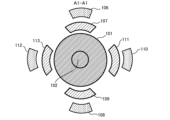
- 5 is a cross-sectional view taken along the A1-A1 plane of FIG. 4.
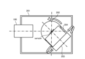
- FIG. 1 is a top view showing an ion milling apparatus equipped with an ion source.
- FIG. 1 is a front view showing an ion milling apparatus equipped with an ion source.
- 13 is a front view showing a case where the rotating stage is tilted with respect to the ion source.
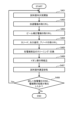
- 11 is a flowchart showing a maintenance procedure when a short circuit occurs inside the ion source.
- 10 is a flowchart showing details of a maintenance procedure for the electrode components.
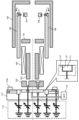
- Fig. 1 is a schematic diagram (cross-sectional view) showing the internal structure of an ion source 100 according to this embodiment.
- Fig. 2A is a cross-sectional view taken along the A-A plane in Fig. 1.
- Fig. 2B is an enlarged view of part B in Fig. 1 when electrodes are attached.
- Fig. 2C is an enlarged view of part C in Fig. 1 when electrodes are attached.
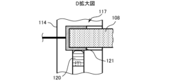
- Fig. 2D is an enlarged view of part D in Fig. 1 when electrodes are attached.
- Fig. 2E is an enlarged view of part E in Fig. 1 when electrodes are attached.
- the ion source 100 includes a first cathode 101, a second cathode 102, an anode 103, a permanent magnet 104, an acceleration electrode 105, a plurality of beam correction electrodes (a first beam correction electrode 106, a second beam correction electrode 108, a third beam correction electrode 110, and a fourth beam correction electrode 112), an electrode component fixing portion 114 (base), a high-voltage power supply 115, and a gas introduction amount adjustment unit 116.
- the high-voltage power supply 115 has a plurality of variable power supplies that apply voltages to each electrode.
- Each beam correction electrode is disposed between the acceleration electrode 105 and the first cathode 101 and the second cathode 102, and the tip (first beam correction electrode tip 107, second beam correction electrode tip 109, third beam correction electrode tip 111, fourth beam correction electrode tip 113) is removable.
- the ion source 100 employs a Penning method, and has a structure in which a cylindrical permanent magnet 104 is arranged on the outer periphery of a cylindrical anode 103, and a disk-shaped first cathode 101 and a disk-shaped second cathode 102 are arranged on both ends of the anode 103.
- a discharge voltage Vd is applied to the anode 103 from a high-voltage power supply 115, and electrons are generated by discharge.
- the generated electrons are influenced by the magnetic field of the permanent magnet 104 arranged on the outer periphery of the anode 103, and the Lorentz force acts on them, causing them to move in a spiral motion inside the anode 103.
- argon is introduced into the ion source via a gas introduction amount adjustment unit 116, it collides with the electrons whose moving distance has increased, generating argon ions.
- the argon ions are attracted to the first cathode 101 and the second cathode 102 by the acceleration voltage Va generated between the anode and the cathode.
- the argon ions are attracted to the second cathode 102, a sputtering phenomenon occurs, causing the second cathode 102 to wear away, and sputtered particles originating from the second cathode 102 are generated.
- the generated sputtering particles adhere to the inner wall and end face of the anode, eventually causing a short circuit between the anode and the cathode.
- argon ions are extracted from a hole in the center of the first cathode 101 and emitted as a beam.
- a negative voltage of about several hundred volts is applied to the acceleration electrode 105, which prevents electrons from escaping from the ion source and electrons from entering from outside the ion source.
- an ion beam correction electrode is provided between the first and second cathodes 101 and 102 and the acceleration electrode 105.
- the ion beam correction electrode is an electrode with four terminals, and each electrode is arranged at 90° intervals.
- the tips of the four ion beam correction electrodes are circular when aligned, and are structured not to interfere with the emission of the ion beam.
- Each of the four terminal electrodes allows the application of correction voltages V c1 , V c2 , V c3 , and V c4 , and can widen or narrow the ion beam.
- the acceleration electrode 105 is fixed by a screw mechanism to a ring portion 114A of the electrode part fixing portion 114 (base). That is, a female screw 114f is provided on the inside of a hole of the ring portion 114A, and a male screw 105m is provided on the outside of the acceleration electrode 105.
- the second cathode 102 is fixed to the electrode part fixing portion 114 by a fixing screw 122.
- the first cathode 101 and the second cathode 102 are attracted to each other by a permanent magnet 104.
- a beam correction electrode (e.g., the second beam correction electrode 108) is detachably connected to the beam correction electrode fixing part 117 of the electrode part fixing part 114 (base), and the beam correction electrode is fixed while connected to a variable power supply.
- a leaf spring 121 is provided inside the beam correction electrode fixing part 117.
- the beam correction electrode is fixed by a set screw 120 while inserted into the beam correction electrode fixing part 117.
- the electrode part fixing part 114 is preferably made of insulating polymeric material, ceramic, or the like that has relatively high heat resistance. Meanwhile, the leaf spring 121 of the beam correction electrode fixing part 117 is made of a metal material that is connected to wiring.
- the beam correction electrode has a pillar portion of a focusing electrode (e.g., the first beam correction electrode 106) that is connected to the electrode part fixing portion 114, and a curved portion (e.g., the first beam correction electrode tip portion 107) at the tip of the pillar portion, which has a curvature centered on the irradiation axis of the ion beam.
- the curved portion is fixed to the pillar portion by a fixing screw 123.
- Figure 3 is a schematic diagram showing how argon ions generated in the ion source sputter the cathode, and how sputtered particles from the cathode adhere to the anode and beam correction electrode.
- the amount of sputtered particles attached to the end surface gradually increases, and eventually electrical conduction occurs between the anode and cathode, as shown in detail 31 in Figure 3.
- electrical conduction occurs, normal discharge will no longer occur, and this can be judged as an indication of when to clean.
- sputtering particles do not usually have a polarity, as shown in detail 32 of FIG. 3, there is a concern that they may adhere to the tip of the ion beam correction electrode, causing a short circuit between the cathode and the ion beam correction electrode or between the acceleration electrode and the ion beam correction electrode. For these reasons, it is desirable to periodically clean the ion beam correction electrode.
- FIG. 4 is a schematic diagram showing the internal structure of the ion source 100 when the acceleration electrode 105 and the beam correction electrode are disassembled.
- FIG. 5 is a cross-sectional view taken along the A1-A1 plane in FIG. 4.
- the acceleration electrode 105 is fixed to the electrode part fixing part 114 by a screw mechanism and can be easily removed. After removing the acceleration electrode 105, the beam correction electrodes (first beam correction electrode 106, second beam correction electrode 108, third beam correction electrode 110, fourth beam correction electrode 112) and the beam correction electrode tips (first beam correction electrode tip 107, second beam correction electrode tip 109, third beam correction electrode tip 111, fourth beam correction electrode tip 113) can be removed.
- the beam correction electrode is fixed by a beam correction electrode fixing part 117 that is connected to a high-voltage power supply 115.
- the beam correction electrode fixing part 117 has a leaf spring 121 made of a highly springy material (such as phosphor bronze), and can be easily inserted to supply power, and can also be easily removed. As shown in Figure 5, each beam correction electrode can be removed from the electrode part fixing part 114, and it is also possible to replace just the tip of the beam correction electrode.
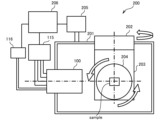
- FIG. 6 is a top view showing an ion milling device 200 equipped with an ion source 100.
- FIG. 7A is a front view showing an ion milling device 200 equipped with an ion source 100.
- FIG. 7B is a front view showing the case where a rotating stage 204 is tilted with respect to the ion source 100.
- the ion milling device 200 includes an ion source 100, a high-voltage power supply 115, a gas introduction amount adjustment unit 116, a sample chamber 201, a stage tilting section 202, a stage arm section 203, a rotating stage 204, an exhaust unit 205, and a control unit 206 (control unit).
- the sample chamber 201 is always kept at a high vacuum (10 ⁇ 3 Pa or less) by the exhaust unit 205 during sample processing.
- the stage tilting section 202 can freely tilt the stage arm section 203 and the rotating stage 204, and can freely adjust the beam irradiation angle with respect to the placed sample.
- the control unit 206 discharges electricity inside the ion source 100, ionizes argon introduced from the gas introduction amount adjustment unit 116, and irradiates the sample as an ion beam.
- the rotating stage 204 rotates constantly during sample processing, allowing the beam to be irradiated evenly onto the sample. If a short circuit occurs inside the ion source 100 during sample processing between the anode and cathode, between the cathode and the beam correction electrode, or between the beam correction electrode and the acceleration electrode, this is fed back to the control unit 206 via the high-voltage power supply 115, and processing is stopped. At this time, the valve in the gas introduction amount adjustment unit 116 closes, stopping the supply of argon to the ion source 100. After stopping, the entire set of electrode parts is removed from the ion source 100 and maintenance is performed.
- FIG. 8 is a flowchart showing the maintenance procedure when a short circuit occurs inside the ion source 100.
- FIG. 8 shows a flowchart of sample processing using the ion milling device 200 equipped with the ion source 100, from the time the processing is completed.
- step S 301 after a sample is placed on the rotating stage 204 , the exhaust unit 205 evacuates the sample chamber 201 to a vacuum.
- the control unit 206 determines the output conditions of the ion beam (acceleration voltage Va, discharge voltage Vd, correction voltages Vc1 , Vc2 , Vc3 , and Vc4 , and gas flow rate) and the stage tilt angle.
- step S303 the control unit 206 applies a voltage to the ion source 100. After the application, sample processing is started.
- step S304 the control unit 206 determines whether or not a short circuit has occurred between the electrodes (between the anode and cathode, the cathode and the beam correction electrode, or the beam correction electrode and the acceleration electrode) during machining. If it is determined that a short circuit has occurred (step S304, Yes), the process proceeds to step S305. On the other hand, if it is determined that a short circuit has not occurred (step S304, No), the process proceeds to step S306.
- step S305 the control unit 206 stops the application of voltage from the high voltage power supply 115. After stopping the application, maintenance is performed on the inside of the ion source 100. The maintenance procedure will be described with reference to the flowchart of FIG.
- step S306 the control unit 206 determines whether or not the sample processing has been completed. If the sample processing has not been completed (step S306, No), the control unit 206 returns to step S304. If the sample processing has been completed (step S306, Yes), the control unit 206 proceeds to step S307. In step S307, the control unit 206 opens the sample chamber 201 to the atmosphere, and ends the sample processing.
- Fig. 9 is a flow chart showing details of the maintenance procedure of the electrode parts.
- Fig. 9 shows a flow chart from the start to the end of the maintenance of the electrode parts shown in step S305 of Fig. 8.
- Figs. 1 and 2A are referred to as appropriate.
- the control unit 206 opens the sample chamber 201 to the atmosphere.
- step S402 after the sample chamber 201 is opened to the atmosphere, the acceleration electrode 105 is removed from the ion source 100.
- step S403 the four beam correction electrodes (first beam correction electrode 106, second beam correction electrode 108, third beam correction electrode 110, fourth beam correction electrode 112) and the beam correction electrode tips (first beam correction electrode tip 107, second beam correction electrode tip 109, third beam correction electrode tip 111, fourth beam correction electrode tip 113) are removed.
- step S404 the first cathode 101, the second cathode 102, the permanent magnet 104, and the anode 103 are removed.
- step S405 each electrode part removed in steps S402 to S404 is cleaned to remove any adhering sputtering particles. If any wear is observed due to argon ion sputtering, they are replaced with new ones.
- step S406 the ion source 100 is reassembled using the electrode parts cleaned in step S405.
- step S407 the sample chamber 201 is evacuated to a vacuum.
- step S408 the control unit 206 applies a voltage to the ion source 100 and determines whether or not a short circuit has occurred between the electrodes. If it is determined again that a short circuit has occurred (step S408, Yes), the process returns to step S401. If there is no problem (step S408, No), the process ends and resumes from step S303 in FIG. 8.
- the ion milling apparatus 200 having an ion source 100 equipped with an acceleration electrode 105 capable of applying a voltage so as to extract the generated ions to the outside in a Penning discharge manner, and a control unit (control unit 206), the ion source 100 has a plurality of focusing electrodes (e.g., a first beam correction electrode 106) whose tips (e.g., a tip 107 of the first beam correction electrode) are removable and disposed between the acceleration electrode 105 and the cathode (first cathode 101, second cathode 102) of the ion source 100, and a plurality of variable power supplies (high voltage power supplies 115) capable of applying a voltage to each of the focusing electrodes, and the control unit corrects the irradiation position of the ion beam by the focusing electrode to which
- the focusing electrode is detachably connected to the base (electrode part fixing part 114) to which the cathode is connected, and a fixing part (beam correction electrode fixing part 117) is provided to fix the focusing electrode while it is connected to the variable power supply. This allows the focusing electrode to be easily removed and attached during maintenance.
- the focusing electrode has a column portion (e.g., the first beam correction electrode 106) connected to a base to which the cathode is connected, and a curved portion (e.g., the first beam correction electrode tip portion 107) at the tip of the column portion, the curved portion having a curvature centered on the irradiation axis of the ion beam. This allows the tip portion of the focusing electrode to be easily removed and attached during maintenance.
- the fixing part can fix the focusing electrode with a screw (see Figure 2D).
- a maintenance method for an ion milling device 200 that includes an ion source 100 having an acceleration electrode 105 that can apply a voltage to draw the generated ions to the outside using a Penning discharge method, the ion source 100 having a plurality of focusing electrodes arranged between the acceleration electrode 105 of the ion source 100 and the cathode, and a plurality of variable power supplies that can apply a voltage to each of the focusing electrodes, the tip of the focusing electrode having a removable curved portion having a curvature centered on the irradiation axis of the ion beam of the focusing electrode, and when performing maintenance, the acceleration electrode can be removed, the curved portion can be removed from the focusing electrode, and the curved portion can be repaired. This makes it easy to perform maintenance when a short circuit occurs between the electrode parts of the ion source.
- the ion source 100 has a base to which the cathode is connected, and a fixing part for fixing the focusing electrode while connected to a variable power supply. After removing the accelerating electrode, the focusing electrode can be removed from the fixing part of the base, and the curved part of the focusing electrode can be repaired. This makes it easy to perform maintenance when a short circuit occurs between electrode parts of the ion source.
- the ion source 100 is equipped with an ion milling device 200 that uses a Penning discharge method and has an acceleration electrode 105 to which a voltage can be applied so as to draw the generated ions to the outside.
- the ion source 100 is a focus electrode of the ion milling device 200 that has multiple focus electrodes arranged between the acceleration electrode 105 and the cathode of the ion source 100 and multiple variable power supplies that can apply a voltage to each of the focus electrodes, and has a column portion that is detachably connected to a base to which the cathode is connected, and a curved portion at the tip of the column portion that has a curvature centered on the irradiation axis of the ion beam. This makes it easy to maintain the focus electrode when a short circuit occurs between the electrode parts of the ion source.
- the curved portion is removable from the focusing electrode. This makes it easy to maintain the curved portion when a short occurs between the electrode components of the ion source.
- the ion source 100 of the ion milling device 200 has a problem in that machining position deviation occurs due to temperature rise of the electrode parts with variable acceleration voltage and voltage application time.
- a correction electrode focus electrode
- the correction electrode has a structure that allows it to be easily removed, and only the tip part that becomes contaminated or worn out can be replaced. This makes it possible to easily incorporate the correction electrode (focus electrode) into the ion source 100 of the ion milling device 200.
- the present invention is not limited to the above-described embodiments, but includes various modified examples.
- the above-described embodiments have been described in detail to clearly explain the present invention, and the present invention is not necessarily limited to those having all of the configurations described.
Landscapes
- Chemical & Material Sciences (AREA)
- Engineering & Computer Science (AREA)
- Analytical Chemistry (AREA)
- Combustion & Propulsion (AREA)
- Physics & Mathematics (AREA)
- Plasma & Fusion (AREA)
- Electron Sources, Ion Sources (AREA)
Abstract
Description
図1は、本実施形態に係るイオン源100の内部構造を示した模式図(断面図)である。図2Aは、図1のA―A面における断面視図である。図2Bは、図1のB部の電極取付け時の拡大図である。図2Cは、図1のC部の電極取付け時の拡大図である。図2Dは、図1のD部の電極取付け時の拡大図である。図2Eは、図1のE部の電極取付け時の拡大図である。
図2Bに示すように、加速電極105は、電極部品固定部114(ベース)のリング部114Aとねじ機構で固定されている。すなわち、リング部114Aの穴の内側にめねじ114fがあり、加速電極105の外側におねじ105mがある。
ステップS302において、制御ユニット206は、イオンビームの出力条件(加速電圧Va、放電電圧Vd、補正電圧Vc1、Vc2、Vc3、Vc4、ガス流量)及びステージ傾斜角度を決定する。
ステップS303において、制御ユニット206は、イオン源100に電圧を印加する。そして、印加後に試料加工を開始する。
ステップS306において、制御ユニット206は、試料加工が完了したか否かを判定し、試料加工が完了していない場合(ステップS306,No)、ステップS304に戻り、試料加工が完了している場合(ステップS306,Yes)、ステップS307に進む。
ステップS307において、制御ユニット206は、試料室201内を大気開放し、試料加工を終了する。
ステップS401において、制御ユニット206は、試料室201の大気開放を行う。
ステップS407において、試料室201内の真空排気を行う。
ステップS408において、制御ユニット206は、イオン源100に電圧を印加し、電極間の短絡が発生したか否かを判定する。再度短絡が発生したと判定した場合(ステップS408,Yes)、ステップS401に戻る。問題がない場合(ステップS408,No)は処理を終了し、図8のステップS303から再開する。
(1)ペニング放電方式で、生成したイオンを外部に引き出すように電圧を印加できる加速電極105を備えたイオン源100と、制御部(制御ユニット206)とを有するイオンミリング装置200において、イオン源100は、イオン源100の加速電極105とカソード(第1のカソード101、第2のカソード102)間に配置された、先端部(例えば、第1のビーム補正電極先端部107)を取り外し可能な複数本の収束電極(例えば、第1のビーム補正電極106)と、各々の前記収束電極に対して電圧を印加できる複数個の可変電源(高圧電源115)と、を有し、制御部は、アノード103とカソード間で発生させたイオンをビームとして引き出すときに、電圧印加された収束電極によってイオンビームの照射位置を補正することを特徴とする。これによれば、イオン源の電極部品間の短絡時に容易にメンテナンスが可能となる。
101 第1のカソード
102 第2のカソード
103 アノード
104 永久磁石
105 加速電極
105m おねじ
106 第1のビーム補正電極(収束電極)
107 第1のビーム補正電極先端部(収束電極先端部)
108 第2のビーム補正電極(収束電極)
109 第2のビーム補正電極先端部(収束電極先端部)
110 第3のビーム補正電極(収束電極)
111 第3のビーム補正電極先端部(収束電極先端部)
112 第4のビーム補正電極(収束電極)
113 第4のビーム補正電極先端部(収束電極先端部)
114 電極部品固定部(ベース)
114A リング部
114f めねじ
115 高圧電源
116 ガス導入量調整ユニット
117 ビーム補正電極固定部(固定部)
120 止ねじ
121 板ばね
122 固定ねじ
123 固定ねじ
200 イオンミリング装置
201 試料室
202 ステージ傾斜部
203 ステージアーム部
204 回転ステージ
205 排気ユニット
206 制御ユニット(制御部)
Claims (8)
- ペニング放電方式で、生成したイオンを外部に引き出すように電圧を印加できる加速電極を備えたイオン源と、制御部とを有するイオンミリング装置において、
前記イオン源は、
前記イオン源の加速電極とカソード間に配置された、先端部を取り外し可能な複数本の収束電極と、
各々の前記収束電極に対して電圧を印加できる複数個の可変電源と、を有し、
前記制御部は、アノードとカソード間で発生させたイオンをビームとして引き出すときに、電圧印加された前記収束電極によってイオンビームの照射位置を補正する
ことを特徴とするイオンミリング装置。 - 請求項1に記載のイオンミリング装置において、
前記カソードが接続されたベースに前記収束電極が着脱可能に接続され、前記可変電源に接続された状態で前記収束電極を固定する固定部を有する
ことを特徴とするイオンミリング装置。 - 請求項1に記載のイオンミリング装置において、
前記収束電極は、
前記カソードが接続されたベースへ接続される収束電極の柱部と、
前記柱部の先端に、イオンビームの照射軸を中心とする曲率を有する湾曲部と、を有する
ことを特徴とするイオンミリング装置。 - 請求項2に記載のイオンミリング装置において、
前記固定部は、ねじで前記収束電極を固定する
ことを特徴とするイオンミリング装置。 - ペニング放電方式で、生成したイオンを外部に引き出すように電圧を印加できる加速電極を有するイオン源を備え、
前記イオン源は、前記イオン源の加速電極とカソード間に配置された、複数本の収束電極と、各々の前記収束電極に対して電圧を印加できる複数個の可変電源と、を有するイオンミリング装置のメンテナンス方法であって、
前記収束電極の先端に、取り外し可能である、前記収束電極のイオンビームの照射軸を中心とする曲率を有する湾曲部を有しており、
メンテナンスする際に、前記加速電極を取り外し、前記収束電極から前記湾曲部を取り外し、前記湾曲部を補修する
ことを特徴とするメンテナンス方法。 - 請求項5に記載のメンテナンス方法において、
前記イオン源は、前記カソードが接続されたベースに前記収束電極が着脱可能に接続され、前記可変電源に接続された状態で前記収束電極を固定する固定部を有しており、
前記加速電極を取り外したのち、前記収束電極を前記ベースの前記固定部から取り外し、前記収束電極の前記湾曲部を補修する
ことを特徴とするメンテナンス方法。 - ペニング放電方式で、生成したイオンを外部に引き出すように電圧を印加できる加速電極を有するイオン源とを備え、
前記イオン源は、前記イオン源の加速電極とカソード間に配置された、複数本の収束電極と、各々の前記収束電極に対して電圧を印加できる複数個の可変電源と、を有するイオンミリング装置の収束電極であって、
前記カソードが接続されたベースに着脱可能に接続される柱部と、前記柱部の先端に、イオンビームの照射軸を中心とする曲率を有する湾曲部と、を有する
ことを特徴とするイオンミリング装置の収束電極。 - 請求項7に記載のイオンミリング装置の収束電極において、
前記湾曲部は、前記収束電極から取り外し可能である
ことを特徴とするイオンミリング装置の収束電極。
Priority Applications (3)
| Application Number | Priority Date | Filing Date | Title |
|---|---|---|---|
| PCT/JP2023/012549 WO2024201722A1 (ja) | 2023-03-28 | 2023-03-28 | イオンミリング装置、メンテナンス方法及びイオンミリング装置の収束電極 |
| KR1020257031255A KR20250151497A (ko) | 2023-03-28 | 2023-03-28 | 이온 밀링 장치, 메인터넌스 방법 및 이온 밀링 장치의 집속 전극 |
| JP2025509344A JPWO2024201722A1 (ja) | 2023-03-28 | 2023-03-28 |
Applications Claiming Priority (1)
| Application Number | Priority Date | Filing Date | Title |
|---|---|---|---|
| PCT/JP2023/012549 WO2024201722A1 (ja) | 2023-03-28 | 2023-03-28 | イオンミリング装置、メンテナンス方法及びイオンミリング装置の収束電極 |
Publications (1)
| Publication Number | Publication Date |
|---|---|
| WO2024201722A1 true WO2024201722A1 (ja) | 2024-10-03 |
Family
ID=92903555
Family Applications (1)
| Application Number | Title | Priority Date | Filing Date |
|---|---|---|---|
| PCT/JP2023/012549 Ceased WO2024201722A1 (ja) | 2023-03-28 | 2023-03-28 | イオンミリング装置、メンテナンス方法及びイオンミリング装置の収束電極 |
Country Status (3)
| Country | Link |
|---|---|
| JP (1) | JPWO2024201722A1 (ja) |
| KR (1) | KR20250151497A (ja) |
| WO (1) | WO2024201722A1 (ja) |
Citations (4)
| Publication number | Priority date | Publication date | Assignee | Title |
|---|---|---|---|---|
| JP2006351374A (ja) * | 2005-06-16 | 2006-12-28 | Jeol Ltd | イオン源 |
| JP2013524467A (ja) * | 2010-04-09 | 2013-06-17 | イー エイ フィシオネ インストルメンツ インコーポレーテッド | 改良型イオン源 |
| WO2018011946A1 (ja) * | 2016-07-14 | 2018-01-18 | 株式会社日立ハイテクノロジーズ | イオンミリング装置 |
| JP2018022701A (ja) * | 2017-09-29 | 2018-02-08 | 株式会社日立ハイテクノロジーズ | イオンガン及びイオンミリング装置、イオンミリング方法 |
-
2023
- 2023-03-28 WO PCT/JP2023/012549 patent/WO2024201722A1/ja not_active Ceased
- 2023-03-28 JP JP2025509344A patent/JPWO2024201722A1/ja active Pending
- 2023-03-28 KR KR1020257031255A patent/KR20250151497A/ko active Pending
Patent Citations (4)
| Publication number | Priority date | Publication date | Assignee | Title |
|---|---|---|---|---|
| JP2006351374A (ja) * | 2005-06-16 | 2006-12-28 | Jeol Ltd | イオン源 |
| JP2013524467A (ja) * | 2010-04-09 | 2013-06-17 | イー エイ フィシオネ インストルメンツ インコーポレーテッド | 改良型イオン源 |
| WO2018011946A1 (ja) * | 2016-07-14 | 2018-01-18 | 株式会社日立ハイテクノロジーズ | イオンミリング装置 |
| JP2018022701A (ja) * | 2017-09-29 | 2018-02-08 | 株式会社日立ハイテクノロジーズ | イオンガン及びイオンミリング装置、イオンミリング方法 |
Also Published As
| Publication number | Publication date |
|---|---|
| JPWO2024201722A1 (ja) | 2024-10-03 |
| KR20250151497A (ko) | 2025-10-21 |
Similar Documents
| Publication | Publication Date | Title |
|---|---|---|
| US6002208A (en) | Universal cold-cathode type ion source with closed-loop electron drifting and adjustable ion-emitting slit | |
| CN109314031B (zh) | 离子铣削装置 | |
| CN107690689A (zh) | 处理室构件的原位电浆清洗 | |
| TWI732817B (zh) | 離子束裝置中汙染控制的裝置和方法 | |
| CN104217913A (zh) | 绝缘结构及绝缘方法 | |
| US20260011524A1 (en) | Multi-beam particle microscope with a quickly replaceable particle source, and method for quickly replacing a particle source in the multi-beam particle microscope | |
| TW202109592A (zh) | 離子槍及離子銑削裝置 | |
| CN105898976B (zh) | 等离子体离子源以及带电粒子束装置 | |
| WO2024201722A1 (ja) | イオンミリング装置、メンテナンス方法及びイオンミリング装置の収束電極 | |
| US10699876B2 (en) | Method of cleaning electrostatic chuck | |
| US12020893B2 (en) | Ion milling device | |
| TWI904110B (zh) | 透鏡、離子植入系統及方法 | |
| US9076625B2 (en) | Indirectly heated cathode cartridge design | |
| KR100485385B1 (ko) | 극성 변환 장치 및 이를 갖는 이온 주입 장치 | |
| US6630677B1 (en) | Electrostatic lens having glassy graphite electrodes | |
| JP7672500B2 (ja) | イオンミリング装置 | |
| JP2010003596A (ja) | 荷電粒子線加工装置 | |
| CN111640639B (zh) | 离子源及其清洁方法 | |
| CN120116029A (zh) | 一种氩气体团簇离子抛光机和金刚石晶体工件的抛光方法 | |
| CN118888422A (zh) | 一种晶圆表面处理装置和方法 | |
| JPH0319314A (ja) | 荷電粒子ビーム露光装置とそのクリーニング方法 |
Legal Events
| Date | Code | Title | Description |
|---|---|---|---|
| 121 | Ep: the epo has been informed by wipo that ep was designated in this application |
Ref document number: 23930362 Country of ref document: EP Kind code of ref document: A1 |
|
| ENP | Entry into the national phase |
Ref document number: 2025509344 Country of ref document: JP Kind code of ref document: A |
|
| WWE | Wipo information: entry into national phase |
Ref document number: 2025509344 Country of ref document: JP |
|
| ENP | Entry into the national phase |
Ref document number: 1020257031255 Country of ref document: KR Free format text: ST27 STATUS EVENT CODE: A-0-1-A10-A15-NAP-PA0105 (AS PROVIDED BY THE NATIONAL OFFICE) |
|
| WWP | Wipo information: published in national office |
Ref document number: 1020257031255 Country of ref document: KR |
|
| NENP | Non-entry into the national phase |
Ref country code: DE |
|
| 122 | Ep: pct application non-entry in european phase |
Ref document number: 23930362 Country of ref document: EP Kind code of ref document: A1 |