WO2024190692A1 - 脈波センサ - Google Patents
脈波センサ Download PDFInfo
- Publication number
- WO2024190692A1 WO2024190692A1 PCT/JP2024/009160 JP2024009160W WO2024190692A1 WO 2024190692 A1 WO2024190692 A1 WO 2024190692A1 JP 2024009160 W JP2024009160 W JP 2024009160W WO 2024190692 A1 WO2024190692 A1 WO 2024190692A1
- Authority
- WO
- WIPO (PCT)
- Prior art keywords
- strain
- pulse wave
- wave sensor
- strain gauges
- load
- Prior art date
- Legal status (The legal status is an assumption and is not a legal conclusion. Google has not performed a legal analysis and makes no representation as to the accuracy of the status listed.)
- Ceased
Links
Images




Classifications
-
- A—HUMAN NECESSITIES
- A61—MEDICAL OR VETERINARY SCIENCE; HYGIENE
- A61B—DIAGNOSIS; SURGERY; IDENTIFICATION
- A61B5/00—Measuring for diagnostic purposes; Identification of persons
- A61B5/02—Detecting, measuring or recording for evaluating the cardiovascular system, e.g. pulse, heart rate, blood pressure or blood flow
- A61B5/024—Measuring pulse rate or heart rate
- A61B5/02444—Details of sensor
-
- A—HUMAN NECESSITIES
- A61—MEDICAL OR VETERINARY SCIENCE; HYGIENE
- A61B—DIAGNOSIS; SURGERY; IDENTIFICATION
- A61B5/00—Measuring for diagnostic purposes; Identification of persons
- A61B5/02—Detecting, measuring or recording for evaluating the cardiovascular system, e.g. pulse, heart rate, blood pressure or blood flow
-
- A—HUMAN NECESSITIES
- A61—MEDICAL OR VETERINARY SCIENCE; HYGIENE
- A61B—DIAGNOSIS; SURGERY; IDENTIFICATION
- A61B5/00—Measuring for diagnostic purposes; Identification of persons
- A61B5/02—Detecting, measuring or recording for evaluating the cardiovascular system, e.g. pulse, heart rate, blood pressure or blood flow
- A61B5/024—Measuring pulse rate or heart rate
- A61B5/02438—Measuring pulse rate or heart rate with portable devices, e.g. worn by the patient
-
- A—HUMAN NECESSITIES
- A61—MEDICAL OR VETERINARY SCIENCE; HYGIENE
- A61B—DIAGNOSIS; SURGERY; IDENTIFICATION
- A61B2562/00—Details of sensors; Constructional details of sensor housings or probes; Accessories for sensors
- A61B2562/02—Details of sensors specially adapted for in-vivo measurements
- A61B2562/0247—Pressure sensors
-
- A—HUMAN NECESSITIES
- A61—MEDICAL OR VETERINARY SCIENCE; HYGIENE
- A61B—DIAGNOSIS; SURGERY; IDENTIFICATION
- A61B2562/00—Details of sensors; Constructional details of sensor housings or probes; Accessories for sensors
- A61B2562/02—Details of sensors specially adapted for in-vivo measurements
- A61B2562/0261—Strain gauges
Definitions
- the present invention relates to a pulse wave sensor.
- Pulse wave sensors are known that detect pulse waves generated when the heart pumps blood.
- One example is a pulse wave sensor that is provided with a pressure plate that acts as a strain-generating body supported so that it can flex when subjected to an external force, and a piezoelectric conversion means that converts the flexure of the pressure plate into an electrical signal.
- the flexible area of the pressure plate is formed in a dome shape that is a convex curved surface facing outward, and a pressure detection element is provided on the inner surface of the top of the pressure plate as a piezoelectric conversion means (see, for example, Patent Document 1).
- the pulse wave sensor needs to detect minute signals, it is necessary to reliably place the detection part close to the subject's radial artery, etc. However, it is difficult to position the detection part of the pulse wave sensor close to the subject's radial artery, etc., which can lead to problems such as a long wearing time before the pulse wave can be obtained and reduced measurement accuracy due to misalignment.
- the present invention was made in consideration of the above points, and aims to reduce the time that a pulse wave sensor is attached to a subject and to improve the measurement accuracy.
- a pulse wave sensor includes a strain gauge having a first surface and a second surface located opposite the first surface, a plurality of intersecting beams provided on the strain gauge, and a load section arranged in the intersecting region of each of the beams on the first surface, a pair of strain gauges arranged on the beams on the second surface, facing each other across the load sections in a plan view, and another pair of strain gauges arranged on the beams intersecting the beams on which the pair of strain gauges are arranged, facing each other across the load sections in a plan view, and detects pulse waves based on changes in resistance values of each of the strain gauges accompanying deformation of the beams.
- the disclosed technology makes it possible to reduce the time that a pulse wave sensor is attached to a subject and improve measurement accuracy.
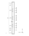
- FIG. 1 is a plan view illustrating a pulse wave sensor according to a first embodiment
- 1 is a cross-sectional view illustrating a pulse wave sensor according to a first embodiment.
- This is the simulation result (part 1) of the amount of strain in the beam caused by the compression of each load part.
- This is the simulation result (part 2) of the amount of strain in the beam caused by the compression of each load part.
- FIG. 1 is a diagram illustrating a bridge connection.
- FIG. 2 is a plan view illustrating the strain gauge according to the first embodiment.
- FIG. 1 is a cross-sectional view (part 1) illustrating a strain gauge according to a first embodiment.
- FIG. 2 is a cross-sectional view (part 2) illustrating the strain gauge according to the first embodiment.
- Fig. 1 is a plan view illustrating a pulse wave sensor according to a first embodiment.
- Fig. 2 is a cross-sectional view illustrating the pulse wave sensor according to the first embodiment, taken along line AA in Fig. 1.
- the pulse wave sensor 1 includes a housing 10, a strain body 20, a wire 30, and a number of strain gauges ( 100L1 , 100L2 , 100L3, 100L4 , 100C1 , 100C2 , 100C3 , 100C4 , 100R1 , 100R2 , 100R3 , 100R4 ).
- the individual strain gauges may be collectively referred to as strain gauge 100.
- the strain body 20 has a base 21, beams 221 , 222 , 223 , and 224 , load portions 231 , 232 , and 233 , and a plurality of extension portions 24.
- the beams may be collectively referred to as beams 22.
- the load portions may be collectively referred to as load portions 23.
- the flexure body 20 is flat.
- the flexure body 20 has a first surface 20m and a second surface 20n located on the opposite side of the first surface 20m.
- the flexure body 20 has, for example, a two-fold symmetric shape in a plan view.
- the flexure body has, for example, a shape with the Y direction as the longitudinal direction and the X direction as the transverse direction.
- the flexure body 20 can be an ellipse, a rectangle, a rounded rectangle, or the like.
- the flexure body 20 is a rounded rectangle with the Y direction as the longitudinal direction.
- a rounded rectangle is a figure in which some or all of the corners of a rectangle are rounded.
- a rounded rectangle may be a shape consisting of two parallel lines of equal length and semicircles arranged at both ends of the parallel lines.
- the material of the flexure body 20 may be, for example, metal, ceramic, glass, etc. Examples of metals used as the material of the flexure body 20 include SUS (stainless steel), copper, aluminum, etc.
- the flexure body 20 may be formed as a single unit, for example, by a press processing method.
- the thickness t of the flexure body 20 excluding the load portion 23 is constant.
- the thickness t of the flexure body 20 excluding the load portion 23 may be, for example, 0.03 mm or more and 0.3 mm or less.
- the side of the pulse wave sensor 1 on which the load portion 23 of the strain body 20 is provided is referred to as the "upper side", and the side on which the load portion 23 of the strain body 20 is not provided is referred to as the "lower side".
- the surface located on the upper side of each part is referred to as the "upper surface”, and the surface located on the lower side of each part is referred to as the "lower surface”.
- the pulse wave sensor 1 can also be used upside down.
- the pulse wave sensor 1 can also be positioned at any angle.
- a planar view refers to viewing an object in a normal direction from the top to the bottom relative to the first surface 20m of the strain body 20.
- a planar shape refers to the shape of the object when viewed in the normal direction.
- the base 21 is a region of a predetermined width on the outer edge of the flexure body 20. Specifically, the base 21 is a ring-shaped region outside the dashed line shown in FIG. 1.
- the width w1 of the base 21 is, for example, 1 mm or more and 5 mm or less.
- the width w1 of the base 21 may or may not be constant.
- the inner length of the base 21 in the X direction is, for example, 5 mm or more and 35 mm or less.
- the inner length of the base 21 in the Y direction is longer than the inner length of the base 21 in the X direction.
- the strain body 20 has a plurality of beams 22 that intersect with each other.
- the plurality of beams 22 may include one beam and a plurality of beams that intersect with the one beam.
- the plurality of beams 22 may be perpendicular to each other.
- Each beam 22 is provided so as to bridge the inside of the base 21.
- the multiple beams 22 include one linear beam 22-4 extending in the Y direction, and linear beams 22-1 , 22-2, and 22-3 extending in the X direction perpendicular to the one beam 22-4 .
- Beam 22-4 is longer than beams 22-1 , 22-2 , and 22-3 .
- beams 22-1 , 22-2 , and 22-3 intersecting with one beam 22-4 are disposed at equal intervals from one another.
- the multiple beams 22 may include four or more beams disposed at equal intervals from one another.
- the width w 2 other than the intersecting region is constant, and is, for example, 1 mm or more and 5 mm or less. It is not essential that the width w 2 be constant, but making the width w 2 constant is preferable in that strain can be detected linearly.
- the multiple beams 22 may include one beam and multiple beams intersecting with the one beam.
- the one beam and the multiple beams intersecting with the one beam do not have to be linear. There may be two or more beams intersecting with the one beam.
- the load portion 23 is disposed in an area where each beam 22 intersects.
- the load portion 231 is disposed in an area where the beams 221 and 224 intersect.
- the load portion 232 is disposed in an area where the beams 222 and 224 intersect.
- the load portion 233 is disposed in an area where the beams 223 and 224 intersect.
- a plurality of load parts 23 are arranged on one beam 224 , so that the load parts 23 affect each other. That is, when one load part 23 is pressed, strain is also generated around the other load parts 23. When any load part 23 is pressed, the sum of the strains generated around each load part 23 is constant.
- the load portions 23 protrude from the upper surface of the beam 22.
- the amount of protrusion of the load portions 23 based on the upper surface of the beam 22 is, for example, approximately 0.1 mm.
- the amount of protrusion of each load portion 23 may or may not be the same.
- the beam 22 is flexible, and elastically deforms when a load is applied to the load portions 23.
- the planar shape of the load portion 23 is, for example, circular, but may also be elliptical, etc.
- the diameter may be, for example, 1.5 mm or more and 2.5 mm or less.
- the planar shape of the load portion 23 is elliptical, it is preferable that the major axis direction faces the Y direction from the viewpoint of making it easier to contact the radial artery.
- the pitch of adjacent load portions 23 can be, for example, about 4 mm or more and 6 mm or less.
- the distance between adjacent load portions 23 can be, for example, about 1 mm or more and 3 mm or less. It is preferable that the distance between adjacent load portions 23 is equal to or less than the diameter of the radial artery. It is generally said that the diameter of the radial artery of 80% of Japanese women is 2.4 mm or more and a maximum of 3.0 mm, and that of 80% of Japanese men is 2.6 mm or more and a maximum of 4.0 mm. In other words, the diameter of the radial artery of 80% of Japanese people is 2.4 mm or more and 4.0 mm or less.
- the spacing between adjacent load parts it is advisable to design the spacing between adjacent load parts to be 4 mm or less, more preferably 3 mm or less, and even more preferably 2.4 mm or less.
- the spacing between adjacent load parts By setting the spacing between adjacent load parts to be 3 mm or less, the probability that one of the load parts will come into contact with the radial artery will be increased in many Japanese subjects.
- the spacing between adjacent load parts By setting the spacing between adjacent load parts to be 2.4 mm or less, the probability that one of the load parts will come into contact with the radial artery will be further increased in an even larger number of Japanese subjects.
- the multiple extensions 24 are sector-shaped or rectangular parts that extend from the inside of the base 21 toward the beam 22 in a plan view.
- a gap (slit) of about 1 mm is provided between each extension 24 and the beam 22.
- the extensions 24 do not contribute to the sensing of the pulse wave sensor 1, so they do not need to be provided.
- the length of the slit extending in the X direction and the length of the slit extending in the Y direction may or may not be the same.
- the length in the X direction of a slit defining a portion of beam 22-1 located on the X+ side of load portion 23-1 may or may not be the same as the length in the Y direction of a slit that is continuous with the slit and defines a portion of beam 22-4 located on the Y- side of load portion 23-1 .
- the wire 30 is a cable that transmits and receives electrical signals between the pulse wave sensor 1 and the outside.
- the wire 30 may be a shielded cable, a flexible board, or the like. Note that the wire 30 is not an essential component of the pulse wave sensor 1.
- the pulse wave sensor 1 may be in a form that communicates with the outside world wirelessly or by other methods without using the wire 30.
- the pulse wave sensor 1 has a pair of strain gauges arranged on the beam 22 on the second surface 20n of the strain body 20, facing each other in a planar view with the load section 23 between them, and another pair of strain gauges arranged on the beam 22 that intersects with the beam 22 on which the pair of strain gauges are arranged, facing each other in a planar view with the load section 23 between them.
- the pulse wave sensor 1 has a pair of strain gauges 100L1 and 100L2 arranged on a beam 221 extending in the X direction on the second surface 20n of the strain body 20, facing each other in a plan view with the load portion 231 therebetween.
- the pulse wave sensor 1 has another pair of strain gauges 100L3 and 100L4 arranged on a beam 224 intersecting the beam 221 on which the pair of strain gauges 100L1 and 100L2 are arranged, facing each other in a plan view with the load portion 231 therebetween.
- the strain gauges 100L1 and 100L2 detect the compressive strain of the beam 22-1 caused by the pressing of the load section 23-1
- the strain gauges 100L3 and 100L4 detect the tensile strain of the beam 22-4 caused by the pressing of the load section 23-1 .
- the distance between the strain gauges 100L1 and 100L2 which detect the compressive strain is wider than the distance between the strain gauges 100L3 and 100L4 which detect the tensile strain.
- the pulse wave sensor 1 also has a pair of strain gauges 100C1 and 100C2 arranged on the beam 222 extending in the X direction on the second surface 20n of the strain body 20, facing each other in a plan view with the load portion 232 therebetween. Also, the pulse wave sensor 1 has another pair of strain gauges 100C3 and 100C4 arranged on the beam 224 intersecting the beam 222 on which the pair of strain gauges 100C1 and 100C2 are arranged , facing each other in a plan view with the load portion 232 therebetween.
- the strain gauges 100C1 and 100C2 detect the compressive strain of the beam 222 caused by the pressing of the load section 232, and the strain gauges 100C3 and 100C4 detect the tensile strain of the beam 224 caused by the pressing of the load section 232.
- the distance between the strain gauges 100C1 and 100C2 which detect the compressive strain is wider than the distance between the strain gauges 100C3 and 100C4 which detect the tensile strain.
- the pulse wave sensor 1 also has a pair of strain gauges 100R1 and 100R2 arranged on the beam 223 extending in the X direction on the second surface 20n of the strain body 20, facing each other across the load portion 233 in a plan view. Also, the pulse wave sensor 1 has another pair of strain gauges 100R3 and 100R4 arranged on the beam 224 intersecting the beam 223 on which the pair of strain gauges 100R1 and 100R2 are arranged, facing each other across the load portion 232 in a plan view.
- the strain gauges 100R1 and 100R2 detect the compressive strain of the beam 223 caused by the pressing of the load section 232
- the strain gauges 100R3 and 100R4 detect the tensile strain of the beam 224 caused by the pressing of the load section 233.
- the distance between the strain gauges 100R1 and 100R2 which detect the compressive strain is wider than the distance between the strain gauges 100R3 and 100R4 which detect the tensile strain.
- each strain gauge 100 By arranging each strain gauge 100 in this way, compressive and tensile strains can be effectively detected and a large output can be obtained by full bridge.
- the pulse wave sensor 1 is used by fixing it to the subject's arm so that one or more of the multiple load sections 23 contact the subject's radial artery.
- the resistance value of the resistor in the strain gauge 100 changes.
- the pulse wave sensor 1 can detect the pulse wave based on the change in the resistance value of the resistor in the strain gauge 100 that accompanies the deformation of the beam 22.
- the pulse wave is output, for example, as a periodic change in voltage from a measurement circuit connected to the electrodes of the strain gauge 100.
- the maximum length of the strain body 20 in the X direction in Figures 1 and 2 was 15 mm
- the maximum length in the Y direction was 25 mm
- the thickness t was 0.1 mm.
- Each load part 23 was circular with a diameter of 2 mm in plan view and a height of 0.1 mm.
- the distance between adjacent load parts 23 was 3 mm. Note that, although the distance between adjacent load parts 23 was set to 3 mm here as an example, it is expected that similar results would be obtained in principle even if the distance was other than 3 mm.
- Fig. 3 shows the results of a simulation (part 1) of the amount of strain in the beam caused by pressing each load part.
- Fig. 4 shows the results of a simulation (part 2) of the amount of strain in the beam caused by pressing each load part.
- Fig. 3 shows the amount of strain when only the load part 23-1 is pressed, and
- Fig. 4 shows the amount of strain when only the load part 23-2 is pressed.
- the part outside L indicates the amount of strain obtained by strain gauges 100L1 and 100L2
- the part inside L indicates the amount of strain obtained by strain gauges 100L3 and 100L4
- the part outside C indicates the amount of strain obtained by strain gauges 100C1 and 100C2
- the part inside C indicates the amount of strain obtained by strain gauges 100C3 and 100C4
- the part outside R indicates the amount of strain obtained by strain gauges 100R1 and 100R2
- the part inside R indicates the amount of strain obtained by strain gauges 100R3 and 100R4 .
- the largest strain amount is obtained by the strain gauges 100.sub.L1 , 100.sub.L2 , 100.sub.L3 , and 100.sub.L4 arranged closest to the load portion 23.sub.1 in the X and Y directions.
- the load portion 23-1 and the load portions 23-2 and 23-3 are disposed on the same beam 22-4 , the effect of pressing the load portion 23-1 also extends to the load portions 23-2 and 23-3 which are not directly pressed. Therefore, as shown in FIG. 3, the amount of strain is detected outside and inside C and outside and inside R.
- Load section 23-2 is closer to load section 23-1 than load section 23-3 . Therefore, the amount of strain of C obtained by strain gauges 100- C1 , 100- C2 , 100- C3 , and 100- C4 is greater than the amount of strain of R obtained by strain gauges 100 -R1 , 100- R2 , 100- R3 , and 100- R4 .
- the largest strain amount is obtained by the strain gauges 100C1 , 100C2 , 100C3 , and 100C4 arranged closest to the load portion 232 in the X and Y directions.
- the load portion 23-2 and the load portions 23-1 and 23-3 are disposed on the same beam 22-4 , the effect of pressing the load portion 23-2 also extends to the load portions 23-1 and 23-3 which are not directly pressed. Therefore, as shown in FIG. 4, the amount of strain is detected outside and inside L and outside and inside R.
- the distance between the load portion 23-2 and the load portion 23-1 is the same as the distance between the load portion 23-2 and the load portion 23-3 . Therefore, the amount of strain of L obtained by the strain gauges 100L1 , 100L2 , 100L3 , and 100L4 is equivalent to the amount of strain of R obtained by the strain gauges 100R1 , 100R2 , 100R3 , and 100R4 .
- the sum of the strain amounts of L, C, and R shown in Fig. 3 coincides with the sum of the strain amounts of L, C, and R shown in Fig. 4.
- the simulation results in the case where only the load portion 233 is pressed are not shown, the strain amounts on the outside and inside of L and the strain amounts on the outside and inside of R in Fig. 3 are interchanged.
- the pulse wave sensor 1 can detect the amount of strain when any one of the multiple load parts 23 is pressed. That is, by fixing the pulse wave sensor 1 to the subject's arm with the arrangement direction of the load parts 23 (Y direction in Figures 1 and 2) facing a direction approximately perpendicular to the extension direction of the radial artery, any one or more of the multiple load parts 23 can be easily applied to the subject's radial artery. And, regardless of which load part 23 is in contact with the subject's radial artery, a constant amount of strain can be obtained. This eliminates the need for a radial artery position detection mechanism or position adjustment, and the pulse wave sensor 1 can be easily fixed to the subject's arm and can reliably detect pulse waves. That is, by using the pulse wave sensor 1, it is possible to shorten the time it is worn on the subject and improve measurement accuracy.
- the pulse wave sensor 1 can obtain a large output by using the four-gauge method in which each strain gauge is connected in a full bridge configuration.
- all of the strain gauges 100 shown in FIG. 1 and FIG. 2 are connected to form one bridge circuit. Specifically, in the plan view shown in FIG. 1, the strain gauges 100 located closest to each load section 23 in the same direction are connected in series to form each side of the bridge circuit.
- strain gauge 100L1 located closest to load section 23-1 in the X-direction, strain gauge 100C1 located closest to load section 23-2 in the X-direction, and strain gauge 100R1 located closest to load section 23-3 in the X-direction are connected in series to form the upper left side of the bridge circuit shown in FIG. 5.
- strain gauge 100L2 located closest to load unit 23-1 in the X+ direction, strain gauge 100C2 located closest to load unit 23-2 in the X+ direction, and strain gauge 100R2 located closest to load unit 23-3 in the X+ direction are connected in series to form the lower right side of the bridge circuit shown in FIG. 5.
- strain gauge 100L3 located closest to load section 231 in the Y-direction, strain gauge 100C3 located closest to load section 232 in the Y-direction, and strain gauge 100R3 located closest to load section 233 in the Y-direction are connected in series to form one upper right side of the bridge circuit shown in Figure 5.
- strain gauge 100L4 located closest to load unit 23-1 in the Y+ direction, strain gauge 100C4 located closest to load unit 23-2 in the Y+ direction, and strain gauge 100R4 located closest to load unit 23-3 in the Y+ direction are connected in series to form the lower left side of the bridge circuit shown in FIG. 5.
- a DC voltage E is supplied between the connection part of the upper left side and the lower left side and the connection part of the upper right side and the lower right side.
- an output voltage e0 can be obtained as the output of the bridge circuit from between the connection part of the upper left side and the upper right side and the connection part of the lower left side and the lower right side.
- the bridge connection may be made inside or outside the housing 10. If necessary, a wiring board for making the bridge connection may be placed inside the housing 10.
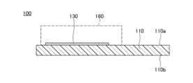
- Fig. 6 is a plan view illustrating the strain gauge according to the first embodiment.
- Fig. 7 is a cross-sectional view (part 1) illustrating the strain gauge according to the first embodiment, showing a cross section along line BB in Fig. 6.
- the strain gauge 100 has a substrate 110, a resistor 130, wiring 140, electrodes 150, and a cover layer 160. That is, the strain gauge 100 has the resistor 130 as a detection element.
- the cover layer 160 can be provided as necessary. For convenience, only the outer edge of the cover layer 160 is shown by a dashed line in Figures 6 and 7. First, each part that constitutes the strain gauge 100 will be described in detail.
- the explanation of the strain gauge using Figures 6 to 8 differs from the other figures in the definition of the upper and lower surfaces.
- the side of the strain gauge 100 on which the resistor 130 of the substrate 110 is provided is referred to as the "upper side", and the side on which the resistor 130 is not provided is referred to as the "lower side”.
- the surface located on the upper side of each part is referred to as the "upper surface”, and the surface located on the lower side of each part is referred to as the "lower surface”.
- the strain gauge 100 can also be used upside down. Also, the strain gauge 100 can be arranged at any angle.
- a planar view refers to viewing an object in a normal direction from the upper side to the lower side relative to the upper surface 110a of the substrate 110.
- a planar shape refers to the shape of the object when the object is viewed in the normal direction.
- the strain gauge 100 is attached to the second surface 20n of the strain body 20 so that the base material 110 faces the second surface 20n of the strain body 20.
- the substrate 110 is a member that serves as a base layer for forming the resistor 130 and the like.
- the substrate 110 is flexible. There are no particular limitations on the thickness of the substrate 110, and it may be determined appropriately depending on the intended use of the strain gauge 100, etc.
- the thickness of the substrate 110 may be approximately 5 ⁇ m to 500 ⁇ m. From the standpoint of strain transmission from the second surface 20n of the strain generating body 20 to the sensing part and dimensional stability against environmental changes, it is preferable that the thickness of the substrate 110 is within the range of 5 ⁇ m to 200 ⁇ m. Also, from the standpoint of insulation, it is preferable that the thickness of the substrate 110 is 10 ⁇ m or more.
- the substrate 110 is formed from an insulating resin film such as PI (polyimide) resin, epoxy resin, PEEK (polyether ether ketone) resin, PEN (polyethylene naphthalate) resin, PET (polyethylene terephthalate) resin, PPS (polyphenylene sulfide) resin, LCP (liquid crystal polymer) resin, polyolefin resin, etc.
- PI polyimide
- epoxy resin epoxy resin
- PEEK polyether ether ketone
- PEN polyethylene naphthalate
- PET polyethylene terephthalate
- PPS polyphenylene sulfide
- LCP liquid crystal polymer
- the insulating resin film may contain fillers, impurities, etc.
- the substrate 110 may be formed from an insulating resin film that contains a filler such as silica or alumina.
- Examples of materials other than resin for the base material 110 include crystalline materials such as SiO 2 , ZrO 2 (including YSZ), Si, Si 2 N 3 , Al 2 O 3 (including sapphire), ZnO, and perovskite ceramics (CaTiO 3 , BaTiO 3 ).
- crystalline materials such as SiO 2 , ZrO 2 (including YSZ), Si, Si 2 N 3 , Al 2 O 3 (including sapphire), ZnO, and perovskite ceramics (CaTiO 3 , BaTiO 3 ).
- amorphous glass or the like may be used as the material for the base material 110.
- Metals such as aluminum, aluminum alloys (duralumin), and titanium may also be used as the material for the base material 110.
- an insulating film is provided so as to cover the upper surface 110a.
- the resistor 130 is a thin film formed in a predetermined pattern on the upper side of the substrate 110.
- the resistor 130 is a sensing part that receives strain and produces a resistance change.
- the resistor 130 may be formed directly on the upper surface 110a of the substrate 110, or may be formed on the upper surface 110a of the substrate 110 via another layer.
- the resistor 130 is shown in FIG. 6 as having a dense matte pattern.
- the resistor 130 has multiple elongated portions arranged at regular intervals with their longitudinal direction in the same direction (the direction of line B-B in the example of FIG. 6), and the ends of adjacent elongated portions are alternately connected, resulting in a zigzag folded structure overall.
- the longitudinal direction of the multiple elongated portions is the grid direction, and the direction perpendicular to the grid direction is the grid width direction (the direction perpendicular to line B-B in the example of FIG. 6).
- One end in the longitudinal direction of the two elongated portions located at the outermost sides in the grid width direction is bent in the grid width direction to form the respective ends 130e1 and 130e2 in the grid width direction of the resistor 130.
- the respective ends 130e1 and 130e2 in the grid width direction of the resistor 130 are electrically connected to the electrodes 150 via the wiring 140.
- the wiring 140 electrically connects the respective ends 130e1 and 130e2 in the grid width direction of the resistor 130 to the respective electrodes 150.
- the resistor 130 can be formed, for example, from a material containing Cr (chromium), a material containing Ni (nickel), or a material containing both Cr and Ni. That is, the resistor 130 can be formed from a material containing at least one of Cr and Ni.
- a material containing Cr is a Cr mixed phase film.
- An example of a material containing Ni is Cu-Ni (copper-nickel).
- An example of a material containing both Cr and Ni is Ni-Cr (nickel-chromium).
- the Cr mixed phase film is a film in which Cr, CrN, Cr 2 N, etc. are mixed together.
- the Cr mixed phase film may contain inevitable impurities such as chromium oxide.
- the thickness of the resistor 130 is not particularly limited and may be appropriately determined depending on the intended use of the strain gauge 100, etc.
- the thickness of the resistor 130 may be approximately 0.05 ⁇ m to 2 ⁇ m.
- the crystallinity of the crystals that make up the resistor 130 for example, the crystallinity of ⁇ -Cr
- the thickness of the resistor 130 is 1 ⁇ m or less, (i) film cracks and (ii) warping of the film from the substrate 110 caused by internal stress of the film that makes up the resistor 130 are reduced.
- the width of resistor 130 is 10 ⁇ m or more and 100 ⁇ m or less. Furthermore, it is preferable that the width of resistor 130 is 10 ⁇ m or more and 70 ⁇ m or less, and more preferably 10 ⁇ m or more and 50 ⁇ m or less.
- the stability of the gauge characteristics can be improved by making the resistor 130 mainly composed of ⁇ -Cr (alpha chromium), which is a stable crystal phase.
- the resistor 130 can make the gauge factor of the strain gauge 100 10 or more, and the gauge factor temperature coefficient TCS and the resistance temperature coefficient TCR within the range of -1000 ppm/°C to +1000 ppm/°C by making the resistor 130 mainly composed of ⁇ -Cr.
- the "main component” means a component that occupies 50% by weight or more of the total material that constitutes the resistor.
- the resistor 130 contains 80% by weight or more of ⁇ -Cr. Furthermore, from the same viewpoint, it is more preferable that the resistor 130 contains 90% by weight or more of ⁇ -Cr.
- ⁇ -Cr is Cr with a bcc structure (body-centered cubic lattice structure).
- the Cr mixed-phase film preferably contains 20% by weight or less of CrN and Cr 2 N.
- the Cr mixed-phase film preferably contains 20% by weight or less of CrN and Cr 2 N.
- the ratio of CrN and Cr 2 N in the Cr mixed phase film is preferably such that the ratio of Cr 2 N is 80% by weight or more and less than 90% by weight with respect to the total weight of CrN and Cr 2 N. More specifically, it is more preferable that the ratio of Cr 2 N is 90% by weight or more and less than 95% by weight with respect to the total weight of CrN and Cr 2 N.
- Cr 2 N has a semiconductor property. Therefore, by setting the ratio of Cr 2 N to 90% by weight or more and less than 95% by weight, the decrease in TCR (negative TCR) becomes more significant. Furthermore, by setting the ratio of Cr 2 N to 90% by weight or more and less than 95% by weight, the ceramicization of the resistor 130 can be reduced, and the brittle fracture of the resistor 130 can be made less likely to occur.
- CrN has the advantage of being chemically stable. By including more CrN in the Cr mixed-phase film, the possibility of unstable N being generated can be reduced, and a stable strain gauge can be obtained.
- "unstable N” means a trace amount of N2 or atomic N that may be present in the Cr mixed-phase film. These unstable N may escape to the outside of the film depending on the external environment (e.g., high temperature environment). When unstable N escapes to the outside of the film, the film stress of the Cr mixed-phase film may change.
- the strain gauge 100 when a Cr mixed-phase film is used as the material for the resistor 130, high sensitivity and miniaturization can be achieved.
- the output of a conventional strain gauge was about 0.04 mV/2 V
- an output of 0.3 mV/2 V or more can be obtained.
- the size (gauge length x gauge width) of a conventional strain gauge was about 3 mm x 3 mm
- the size (gauge length x gauge width) can be miniaturized to about 0.3 mm x 0.3 mm.
- the wiring 140 is provided on the substrate 110.
- the wiring 140 is electrically connected to the resistor 130 and the electrode 150.
- the wiring 140 is not limited to being linear, and can be in any pattern.
- the wiring 140 can also be of any width and length.
- the wiring 140 is shown in FIG. 6 as having a matte pattern with a lower density than the resistor 130.
- the electrodes 150 are provided on the substrate 110.
- the electrodes 150 are electrically connected to the resistor 130 via the wiring 140.
- the electrodes 150 are formed in a substantially rectangular shape wider than the wiring 140 in a plan view.
- the electrodes 150 are a pair of electrodes for outputting the change in resistance value of the resistor 130 caused by distortion to the outside.
- a lead wire for external connection is joined to the electrodes 150.
- a metal layer with low resistance such as copper or a metal layer with good solderability such as gold may be laminated on the upper surface of the electrode 150.
- the resistor 130, the wiring 140, and the electrodes 150 are denoted by different reference numerals for convenience, they can be integrally formed from the same material in the same process. Note that in FIG. 6, the electrodes 150 are shown with a matte pattern of the same density as the wiring 140 for convenience.
- the cover layer 160 (protective layer) is provided on the upper surface 110a of the substrate 110 as necessary, so as to cover the resistor 130 and the wiring 140 and expose the electrodes 150.
- materials for the cover layer 160 include insulating resins such as PI resin, epoxy resin, PEEK resin, PEN resin, PET resin, PPS resin, and composite resins (e.g., silicone resin, polyolefin resin).
- the cover layer 160 may contain a filler or a pigment.
- the thickness of the cover layer 160 can be about 2 ⁇ m to 30 ⁇ m.
- a resistor 130, wiring 140, electrodes 150, and a cover layer 160 are formed on a substrate 110.
- another layer (such as a functional layer described later) may be formed between the substrate 110 and the layers of these components.
- a method for manufacturing the strain gauge 100 is described.
- a substrate 110 is prepared, and a metal layer (for convenience, referred to as metal layer A) is formed on the upper surface 110a of the substrate 110.
- Metal layer A is a layer that is ultimately patterned to become resistor 130, wiring 140, and electrode 150. Therefore, the material and thickness of metal layer A are the same as the material and thickness of resistor 130, wiring 140, and electrode 150 described above.
- the metal layer A can be formed, for example, by magnetron sputtering using a raw material capable of forming the metal layer A as a target. Instead of magnetron sputtering, the metal layer A may be formed using reactive sputtering, vapor deposition, arc ion plating, pulsed laser deposition, or the like. After the metal layer A is formed on the upper surface 110a of the substrate 110, the metal layer A is patterned into a planar shape similar to the resistor 130, wiring 140, and electrode 150 in FIG. 6 by a well-known photolithography method.
- a base layer may be formed on the upper surface 110a of the substrate 110 before forming the metal layer A.
- a functional layer of a predetermined thickness may be vacuum-deposited on the upper surface 110a of the substrate 110 by a conventional sputtering method.
- the functional layer refers to a layer that has the function of promoting the crystal growth of at least the upper layer, metal layer A (resistor 130).
- the functional layer preferably also has the function of preventing oxidation of metal layer A due to oxygen or moisture contained in the substrate 110, and/or the function of improving adhesion between the substrate 110 and metal layer A.
- the functional layer may also have other functions.
- the insulating resin film that constitutes the substrate 110 may contain oxygen and moisture, and Cr may form a self-oxidized film. Therefore, particularly when the metal layer A contains Cr, it is preferable to form a functional layer that has the function of preventing oxidation of the metal layer A.
- the material of the functional layer may be, for example, one or more metals selected from the group consisting of Cr (chromium), Ti (titanium), V (vanadium), Nb (niobium), Ta (tantalum), Ni (nickel), Y (yttrium), Zr (zirconium), Hf (hafnium), Si (silicon), C (carbon), Zn (zinc), Cu (copper), Bi (bismuth), Fe (iron), Mo (molybdenum), W (tungsten), Ru (ruthenium), Rh (rhodium), Re (rhenium), Os (osmium), Ir (iridium), Pt (platinum), Pd (palladium), Ag (silver), Au (gold), Co (cobalt), Mn (manganese), and Al (aluminum), an alloy of any of the metals in this group, or a compound of any of the metals in this group.
- Cr chromium
- Ti titanium
- V vanadium
- FIG. 8 is a cross-sectional view (part 2) illustrating the strain gauge according to the first embodiment.
- FIG. 8 shows the cross-sectional shape of the strain gauge 100 when a functional layer 120 is provided as an underlayer for the resistor 130, wiring 140, and electrode 150.
- the planar shape of the functional layer 120 may be patterned to be substantially the same as the planar shapes of the resistor 130, the wiring 140, and the electrodes 150, for example. However, the planar shapes of the functional layer 120 and the resistor 130, the wiring 140, and the electrodes 150 do not have to be substantially the same.
- the functional layer 120 when the functional layer 120 is formed from an insulating material, the functional layer 120 may be patterned to be different from the planar shapes of the resistor 130, the wiring 140, and the electrodes 150.
- the functional layer 120 may be formed in a solid shape in the area where the resistor 130, the wiring 140, and the electrodes 150 are formed, for example.
- the functional layer 120 may be formed in a solid shape on the entire upper surface of the substrate 110.
- a cover layer 160 is formed on the upper surface 110a of the substrate 110 as necessary.
- the cover layer 160 covers the resistor 130 and wiring 140, but the electrodes 150 may be exposed from the cover layer 160.
- the cover layer 160 can be formed by laminating a semi-cured thermosetting insulating resin film on the upper surface 110a of the substrate 110 so as to cover the resistor 130 and wiring 140 and expose the electrodes 150, and then heating and curing the insulating resin film. Through the above steps, the strain gauge 100 is completed.
- the pulse wave sensor according to the present disclosure is not limited to the above-described embodiments and modifications.
- various modifications and substitutions can be made to the pulse wave sensor according to the above-described embodiments and the like without departing from the scope of the claims.
- one beam 224 is provided on which the strain gauges 100 for detecting tensile strains marked with the symbols L, C, and R in Fig. 1 are arranged.
- three independent beams extending in the Y direction may be provided for the strain gauges 100 for detecting tensile strains marked with the symbols L, C, and R in Fig. 1.
- the amount of strain can be detected by providing one bridge circuit for the four strain gauges 100 marked with the symbols L in Fig. 1, one bridge circuit for the four strain gauges 100 marked with the symbols C, and one bridge circuit for the four strain gauges 100 marked with the symbols R.
- the number of load sections 23 is not limited to three, but may be two or more. Of course, the number of load sections 23 may be four or more. Furthermore, the arrangement of the load sections 23 is not limited to a single row, but may be multiple rows.
- the pulse wave sensor 1 etc. detects a pulse wave
- the detection target of the pulse wave sensor 1 is not limited to a pulse wave.
- the pulse wave sensor 1 etc. can detect, for example, pulse pressure, blood pressure, pulse rate, oxygen level, etc.
- 1 Pulse wave sensor 10 Housing, 20 Strain generating body, 20m First surface, 20n Second surface, 21 Base, 221 , 222 , 223 , 224 Beam, 231 , 232 , 233 Load section, 24 Extension section, 30 Wire, 100L1 , 100L2 , 100L3 , 100L4 , 100C1, 100C2, 100C3 , 100C4, 100R1, 100R2 , 100R3 , 100R4 Strain gauge, 110 Base material, 110a Top surface, 130 Resistor, 140 Wiring , 150 Electrode, 160 Cover layer, 130e1 , 130e 2 termination
Landscapes
- Health & Medical Sciences (AREA)
- Life Sciences & Earth Sciences (AREA)
- Cardiology (AREA)
- Biomedical Technology (AREA)
- Medical Informatics (AREA)
- Biophysics (AREA)
- Pathology (AREA)
- Engineering & Computer Science (AREA)
- Physiology (AREA)
- Heart & Thoracic Surgery (AREA)
- Physics & Mathematics (AREA)
- Molecular Biology (AREA)
- Surgery (AREA)
- Animal Behavior & Ethology (AREA)
- General Health & Medical Sciences (AREA)
- Public Health (AREA)
- Veterinary Medicine (AREA)
- Measurement Of Force In General (AREA)
- Measuring Pulse, Heart Rate, Blood Pressure Or Blood Flow (AREA)
Priority Applications (3)
| Application Number | Priority Date | Filing Date | Title |
|---|---|---|---|
| CN202480017401.XA CN120916688A (zh) | 2023-03-14 | 2024-03-08 | 脉搏波传感器 |
| KR1020257029876A KR20250142440A (ko) | 2023-03-14 | 2024-03-08 | 맥파 센서 |
| EP24770798.7A EP4681623A1 (en) | 2023-03-14 | 2024-03-08 | Pulse wave sensor |
Applications Claiming Priority (2)
| Application Number | Priority Date | Filing Date | Title |
|---|---|---|---|
| JP2023040008A JP2024130342A (ja) | 2023-03-14 | 2023-03-14 | 脈波センサ |
| JP2023-040008 | 2023-03-14 |
Publications (1)
| Publication Number | Publication Date |
|---|---|
| WO2024190692A1 true WO2024190692A1 (ja) | 2024-09-19 |
Family
ID=92755815
Family Applications (1)
| Application Number | Title | Priority Date | Filing Date |
|---|---|---|---|
| PCT/JP2024/009160 Ceased WO2024190692A1 (ja) | 2023-03-14 | 2024-03-08 | 脈波センサ |
Country Status (5)
| Country | Link |
|---|---|
| EP (1) | EP4681623A1 (https=) |
| JP (1) | JP2024130342A (https=) |
| KR (1) | KR20250142440A (https=) |
| CN (1) | CN120916688A (https=) |
| WO (1) | WO2024190692A1 (https=) |
Citations (6)
| Publication number | Priority date | Publication date | Assignee | Title |
|---|---|---|---|---|
| JP2000005139A (ja) * | 1998-06-23 | 2000-01-11 | Seiko Epson Corp | 脈波検出装置および触覚検出装置 |
| JP2002078689A (ja) | 2000-09-05 | 2002-03-19 | Kishino Masakata | 圧脈波検出具 |
| JP2006043445A (ja) * | 2004-07-07 | 2006-02-16 | Showa Denko Kk | 生体情報計測用パネル、生体情報計測用マット、生体情報計測装置及び生体情報計測方法 |
| JP2022175355A (ja) * | 2021-05-13 | 2022-11-25 | ミネベアミツミ株式会社 | 脈波センサ |
| JP2022182909A (ja) * | 2021-05-26 | 2022-12-08 | ミネベアミツミ株式会社 | バイタルセンサ |
| JP2023040008A (ja) | 2016-12-11 | 2023-03-22 | シナジー・ダーマトロジー・リミテッド | 硫酸化多糖を含む組成物 |
-
2023
- 2023-03-14 JP JP2023040008A patent/JP2024130342A/ja active Pending
-
2024
- 2024-03-08 WO PCT/JP2024/009160 patent/WO2024190692A1/ja not_active Ceased
- 2024-03-08 KR KR1020257029876A patent/KR20250142440A/ko active Pending
- 2024-03-08 EP EP24770798.7A patent/EP4681623A1/en active Pending
- 2024-03-08 CN CN202480017401.XA patent/CN120916688A/zh active Pending
Patent Citations (6)
| Publication number | Priority date | Publication date | Assignee | Title |
|---|---|---|---|---|
| JP2000005139A (ja) * | 1998-06-23 | 2000-01-11 | Seiko Epson Corp | 脈波検出装置および触覚検出装置 |
| JP2002078689A (ja) | 2000-09-05 | 2002-03-19 | Kishino Masakata | 圧脈波検出具 |
| JP2006043445A (ja) * | 2004-07-07 | 2006-02-16 | Showa Denko Kk | 生体情報計測用パネル、生体情報計測用マット、生体情報計測装置及び生体情報計測方法 |
| JP2023040008A (ja) | 2016-12-11 | 2023-03-22 | シナジー・ダーマトロジー・リミテッド | 硫酸化多糖を含む組成物 |
| JP2022175355A (ja) * | 2021-05-13 | 2022-11-25 | ミネベアミツミ株式会社 | 脈波センサ |
| JP2022182909A (ja) * | 2021-05-26 | 2022-12-08 | ミネベアミツミ株式会社 | バイタルセンサ |
Non-Patent Citations (1)
| Title |
|---|
| See also references of EP4681623A1 |
Also Published As
| Publication number | Publication date |
|---|---|
| EP4681623A1 (en) | 2026-01-21 |
| CN120916688A (zh) | 2025-11-07 |
| JP2024130342A (ja) | 2024-09-30 |
| KR20250142440A (ko) | 2025-09-30 |
Similar Documents
| Publication | Publication Date | Title |
|---|---|---|
| JP7570975B2 (ja) | ひずみゲージ | |
| EP4338663A1 (en) | Pulse wave sensor | |
| US12306053B2 (en) | Strain gauge including a barrier layer over a resistance body | |
| US20250009242A1 (en) | Pulse wave measuring device | |
| JP7755708B2 (ja) | ひずみゲージ | |
| JP7571976B2 (ja) | 脈波センサ | |
| JP7537836B2 (ja) | バイタルセンサ | |
| WO2024190692A1 (ja) | 脈波センサ | |
| WO2024029538A1 (ja) | ひずみゲージ | |
| JP2024117474A (ja) | 押圧力センサ | |
| JP7436581B1 (ja) | ひずみゲージ | |
| CN119137441B (zh) | 应变计 | |
| US20250228464A1 (en) | Pulse wave sensor | |
| EP4691351A1 (en) | Pulse wave sensor | |
| US20250155306A1 (en) | Pulse wave sensor | |
| US12595998B2 (en) | Strain gauge | |
| JP2024179645A (ja) | 脈波測定装置 | |
| WO2022249717A1 (ja) | バイタルセンサ | |
| JP2024143982A (ja) | 脈波センサ | |
| WO2024204574A1 (ja) | 脈波センサ | |
| JP2024175547A (ja) | 脈波測定装置 | |
| JP2024098234A (ja) | 脈波センサ | |
| JP2024006486A (ja) | バイタルセンサ | |
| JP2024088419A (ja) | ひずみゲージ | |
| WO2024010027A1 (ja) | ひずみゲージ |
Legal Events
| Date | Code | Title | Description |
|---|---|---|---|
| 121 | Ep: the epo has been informed by wipo that ep was designated in this application |
Ref document number: 24770798 Country of ref document: EP Kind code of ref document: A1 |
|
| ENP | Entry into the national phase |
Ref document number: 1020257029876 Country of ref document: KR Free format text: ST27 STATUS EVENT CODE: A-0-1-A10-A15-NAP-PA0105 (AS PROVIDED BY THE NATIONAL OFFICE) |
|
| WWE | Wipo information: entry into national phase |
Ref document number: 202480017401.X Country of ref document: CN |
|
| WWE | Wipo information: entry into national phase |
Ref document number: 2024770798 Country of ref document: EP |
|
| NENP | Non-entry into the national phase |
Ref country code: DE |
|
| WWP | Wipo information: published in national office |
Ref document number: 202480017401.X Country of ref document: CN |
|
| ENP | Entry into the national phase |
Ref document number: 2024770798 Country of ref document: EP Effective date: 20251014 |
|
| ENP | Entry into the national phase |
Ref document number: 2024770798 Country of ref document: EP Effective date: 20251014 |
|
| ENP | Entry into the national phase |
Ref document number: 2024770798 Country of ref document: EP Effective date: 20251014 |
|
| ENP | Entry into the national phase |
Ref document number: 2024770798 Country of ref document: EP Effective date: 20251014 |
|
| ENP | Entry into the national phase |
Ref document number: 2024770798 Country of ref document: EP Effective date: 20251014 |