WO2024190397A1 - 電子装置 - Google Patents
電子装置 Download PDFInfo
- Publication number
- WO2024190397A1 WO2024190397A1 PCT/JP2024/007012 JP2024007012W WO2024190397A1 WO 2024190397 A1 WO2024190397 A1 WO 2024190397A1 JP 2024007012 W JP2024007012 W JP 2024007012W WO 2024190397 A1 WO2024190397 A1 WO 2024190397A1
- Authority
- WO
- WIPO (PCT)
- Prior art keywords
- resin
- electronic device
- terminal
- die pad
- lead
- Prior art date
- Legal status (The legal status is an assumption and is not a legal conclusion. Google has not performed a legal analysis and makes no representation as to the accuracy of the status listed.)
- Ceased
Links
Images









Classifications
-
- H—ELECTRICITY
- H10—SEMICONDUCTOR DEVICES; ELECTRIC SOLID-STATE DEVICES NOT OTHERWISE PROVIDED FOR
- H10W—GENERIC PACKAGES, INTERCONNECTIONS, CONNECTORS OR OTHER CONSTRUCTIONAL DETAILS OF DEVICES COVERED BY CLASS H10
- H10W74/00—Encapsulations, e.g. protective coatings
- H10W74/10—Encapsulations, e.g. protective coatings characterised by their shape or disposition
- H10W74/111—Encapsulations, e.g. protective coatings characterised by their shape or disposition the semiconductor body being completely enclosed
-
- H—ELECTRICITY
- H10—SEMICONDUCTOR DEVICES; ELECTRIC SOLID-STATE DEVICES NOT OTHERWISE PROVIDED FOR
- H10W—GENERIC PACKAGES, INTERCONNECTIONS, CONNECTORS OR OTHER CONSTRUCTIONAL DETAILS OF DEVICES COVERED BY CLASS H10
- H10W70/00—Package substrates; Interposers; Redistribution layers [RDL]
- H10W70/40—Leadframes
- H10W70/421—Shapes or dispositions
-
- H—ELECTRICITY
- H10—SEMICONDUCTOR DEVICES; ELECTRIC SOLID-STATE DEVICES NOT OTHERWISE PROVIDED FOR
- H10W—GENERIC PACKAGES, INTERCONNECTIONS, CONNECTORS OR OTHER CONSTRUCTIONAL DETAILS OF DEVICES COVERED BY CLASS H10
- H10W72/00—Interconnections or connectors in packages
-
- H—ELECTRICITY
- H10—SEMICONDUCTOR DEVICES; ELECTRIC SOLID-STATE DEVICES NOT OTHERWISE PROVIDED FOR
- H10W—GENERIC PACKAGES, INTERCONNECTIONS, CONNECTORS OR OTHER CONSTRUCTIONAL DETAILS OF DEVICES COVERED BY CLASS H10
- H10W74/00—Encapsulations, e.g. protective coatings
- H10W74/01—Manufacture or treatment
-
- H—ELECTRICITY
- H10—SEMICONDUCTOR DEVICES; ELECTRIC SOLID-STATE DEVICES NOT OTHERWISE PROVIDED FOR
- H10W—GENERIC PACKAGES, INTERCONNECTIONS, CONNECTORS OR OTHER CONSTRUCTIONAL DETAILS OF DEVICES COVERED BY CLASS H10
- H10W90/00—Package configurations
- H10W90/811—Multiple chips on leadframes
Definitions
- This disclosure relates to electronic devices.
- the semiconductor device described in this document includes a conductive support member, a semiconductor element, and a sealing resin.
- the conductive support member includes a die pad and multiple terminals.
- the semiconductor element is mounted on the die pad.
- the multiple terminals are arranged around the die pad.
- the sealing resin collectively seals the die pad, the semiconductor element, and portions of the multiple terminals.
- the sealing resin is formed by transfer molding.
- the lead frame is placed in a metal mold, and fluidized resin is poured into the cavity of the metal mold to fill it, and the resin is then solidified.
- the resin is injected from the center in the left-right direction above the page.
- the area near the resin injection section does not have any parts that will become the terminals (conductive support members) of the lead frame, and is configured not to impede the flow of the resin.
- the fluidized resin is filled forcefully when forming the sealing resin, air is drawn in during the filling, and the air is likely to remain as pinholes (voids) near the resin injection section after the resin is filled. This could lead to poor filling of the sealing resin.
- An object of the present disclosure is to provide an electronic device that is an improvement over conventional electronic devices.
- an object of the present disclosure is to provide an electronic device that is suitable for suppressing poor filling of the sealing resin.
- the electronic device provided by the first aspect of the present disclosure includes a conductive support member, at least one electronic element disposed on one side of the conductive support member in the thickness direction, and a sealing resin covering the at least one electronic element and a part of the conductive support member.
- the sealing resin has a first resin side surface facing one side in a first direction perpendicular to the thickness direction.
- a first gate mark having a rougher surface than other regions of the first resin side surface is formed on the first resin side surface.
- the conductive support member includes a first portion located closest to the first gate mark in the first direction and located inward from the first gate mark in a second direction perpendicular to the thickness direction and the first direction when viewed in the thickness direction.
- a ratio of a first distance, which is the distance between the first gate mark and the first portion in the first direction, to a first dimension, which is the length of the first gate mark in the thickness direction is greater than 0% and is not greater than 500%.
- the electronic device provided by the second aspect of the present disclosure includes a conductive support member, at least one electronic element arranged on one side of the conductive support member in the thickness direction, and a sealing resin covering the at least one electronic element and a part of the conductive support member.
- the sealing resin has a first resin side surface facing one side of a first direction perpendicular to the thickness direction, a second resin side surface facing the other side of the first direction, a third resin side surface facing one side of a second direction perpendicular to the thickness direction and the first direction, and a fourth resin side surface facing the other side of the second direction.
- a first gate mark having a surface rougher than other regions of the first resin side surface is formed on the first resin side surface.
- the conductive support member includes a die pad portion and a plurality of first lead terminals. Each of the plurality of first lead terminals protrudes from the third resin side surface to one side of the second direction.
- the at least one electronic element is mounted on the die pad portion.
- the plurality of first lead terminals are arranged at intervals in the first direction, and include a one-end first terminal located at an end on one side in the first direction.
- the one-end first terminal has a first lead portion, a first pad portion, and a first extension portion.
- the first lead portion is located on one side of the die pad portion in the first direction, and extends in the second direction.
- the first pad portion is connected to an end portion of the first lead portion on the other side in the second direction, and extends to the other side in the first direction.
- the first extension portion is connected to an end portion of the first lead portion on the other side in the second direction, and extends to the other side in the second direction.
- the first extension portion includes a portion located inward from the first gate mark in the second direction when viewed in the thickness direction.
- the above configuration makes it possible to prevent insufficient filling of the sealing resin in electronic devices.
- FIG. 1 is a plan view showing an electronic device according to a first embodiment of the present disclosure.
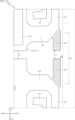
- FIG. 2 is a plan view corresponding to FIG. 1, seen through the sealing resin.
- FIG. 3 is a front view showing the electronic device according to the first embodiment of the present disclosure.
- FIG. 4 is a left side view showing the electronic device according to the first embodiment of the present disclosure.
- FIG. 5 is a rear view showing the electronic device according to the first embodiment of the present disclosure.
- FIG. 6 is a right side view showing the electronic device according to the first embodiment of the present disclosure.
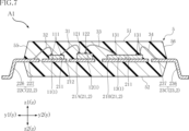
- FIG. 7 is a cross-sectional view taken along line VII-VII in FIG.
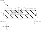
- FIG. 8 is a cross-sectional view taken along line VIII-VIII in FIG.
- FIG. 9 is a partially enlarged view of FIG. FIG.
- FIG. 10 is a plan view illustrating a manufacturing process of the electronic device according to the first embodiment of the present disclosure.
- FIG. 11 is a plan view illustrating a manufacturing process of the electronic device according to the first embodiment of the present disclosure.
- FIG. 12 is a plan view illustrating a manufacturing process of the electronic device according to the first embodiment of the present disclosure.
- FIG. 13 is a plan view showing an electronic device according to a first modified example of the first embodiment, seen through a sealing resin.
- FIG. 14 is a partially enlarged view of FIG.
- FIG. 15 is a plan view showing an electronic device according to a second embodiment of the present disclosure.
- FIG. 16 is a plan view corresponding to FIG. 15, seen through the sealing resin.
- FIG. 17 is a front view showing an electronic device according to a second embodiment of the present disclosure.
- FIG. 18 is a left side view showing an electronic device according to a second embodiment of the present disclosure.
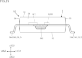
- FIG. 19 is a rear view showing an electronic device according to a second embodiment of the present disclosure.
- FIG. 20 is a right side view showing an electronic device according to a second embodiment of the present disclosure.
- FIG. 21 is a cross-sectional view taken along line XXI-XXI in FIG.
- FIG. 22 is a cross-sectional view taken along line XXII-XXII in FIG.
- FIG. 23 is a circuit configuration diagram of an electronic device according to a second embodiment of the present disclosure.
- FIG. 24 is a plan view showing an electronic device according to a first modified example of the second embodiment, seen through a sealing resin.
- an object A is formed on an object B" and “an object A is formed on an object B” include “an object A is formed directly on an object B” and “an object A is formed on an object B with another object interposed between the object A and the object B” unless otherwise specified.
- an object A is disposed on an object B” and “an object A is disposed on an object B” include “an object A is disposed directly on an object B” and “an object A is disposed on an object B with another object interposed between the object A and the object B" unless otherwise specified.
- an object A is located on an object B includes “an object A is located on an object B in contact with an object B” and “an object A is located on an object B with another object interposed between the object A and the object B” unless otherwise specified.
- an object A overlaps an object B when viewed in a certain direction includes “an object A overlaps the entire object B” and “an object A overlaps a part of an object B.”
- a surface A faces in direction B is not limited to the case where the angle of surface A with respect to direction B is 90°, but also includes the case where surface A is tilted with respect to direction B.
- the electronic device A1 of this embodiment includes a plurality of electronic elements 1, a conductive support member 2, a plurality of wires 31 to 34, and a sealing resin 5.
- the conductive support member 2 includes a die pad portion 21, a plurality of first lead terminals 22, and a plurality of second lead terminals 23.
- the specific use of the electronic device A1 is not limited in any way, but it is, for example, surface-mounted on a wiring board of an inverter device of an electric vehicle or a hybrid vehicle.
- the package format of the electronic device A1 is a small outline package (SOP).
- SOP small outline package
- the package format of the electronic device A1 is not limited to SOP.
- FIGS. 1 and 2 are plan views showing electronic device A1.
- FIG. 3 is a front view showing electronic device A1.
- FIG. 4 is a left side view showing electronic device A1.
- FIG. 5 is a rear view showing electronic device A1.
- FIG. 6 is a right side view showing electronic device A1.
- FIG. 7 is a cross-sectional view taken along line VII-VII in FIG. 2.
- FIG. 8 is a cross-sectional view taken along line VIII-VIII in FIG. 2.
- FIG. 9 is a partially enlarged view of FIG. 2.
- FIG. 2 shows the sealing resin 5 through which light passes. In FIG. 2, the through sealing resin 5 is shown by an imaginary line (two-dot chain line).
- the thickness direction of the die pad portion 21 (conductive support member 2) will be referred to as the "thickness direction z".
- One direction orthogonal to thickness direction z (left-right direction in FIG. 1) will be referred to as the "first direction x”.
- a direction orthogonal to both thickness direction z and first direction x (up-down direction in FIG. 1) will be referred to as the "second direction y”.
- electronic device A1 is rectangular (or approximately rectangular) when viewed in thickness direction z (in a plan view).
- the multiple electronic elements 1 include a first semiconductor element 11, an insulating element 12, and a second semiconductor element 13.
- the first semiconductor element 11, the second semiconductor element 13, and the insulating element 12 are elements that are the functional core of the electronic device A1.
- each of the first semiconductor element 11, the second semiconductor element 13, and the insulating element 12 is composed of individual elements.
- each of the first semiconductor element 11, the second semiconductor element 13, and the insulating element 12 is rectangular with its longer side in the first direction x.
- the first semiconductor element 11 is a controller (control element) of a gate driver that drives switching elements such as IGBTs and MOSFETs.
- the first semiconductor element 11 has a circuit that converts a control signal input from an ECU or the like into a PWM control signal, a transmission circuit for transmitting the PWM control signal to the second semiconductor element 13, and a receiving circuit that receives an electrical signal from the second semiconductor element 13.
- the first semiconductor element 11 is an example of a "first electronic element" in this disclosure.
- the second semiconductor element 13 is a gate driver (drive element) for driving the switching element.
- the second semiconductor element 13 has a receiving circuit for receiving a PWM control signal, a circuit for driving the switching element based on the PWM control signal, and a transmitting circuit for transmitting an electrical signal to the first semiconductor element 11.
- An example of the electrical signal is an output signal from a temperature sensor arranged near the motor.
- the second semiconductor element 13 is an example of a "second electronic element" in this disclosure.
- the insulating element 12 is an element for transmitting a PWM control signal or other electric signals in an insulated state.
- the insulating element 12 is an inductive type.
- An insulating transformer is an example of an inductive type insulating element 12.
- An insulating transformer transmits an electric signal in an insulated state by inductively coupling two inductors (coils).
- the insulating element 12 has a substrate made of silicon.
- An inductor made of copper is formed on the substrate.
- the inductors include a transmitting inductor and a receiving inductor, and these inductors are stacked in the thickness direction z.
- a dielectric layer made of silicon dioxide (SiO 2 ) or the like is interposed between the transmitting inductor and the receiving inductor.
- the transmitting inductor and the receiving inductor are electrically insulated by the dielectric layer.
- the insulating element 12 may be a capacitive type.
- a capacitor is an example of a capacitive type insulating element 12.
- the insulating element 12 may be a photocoupler.
- the second semiconductor element 13 requires a power supply voltage higher than that required for the first semiconductor element 11. This causes a significant potential difference between the first semiconductor element 11 and the second semiconductor element 13.
- the first circuit including the first semiconductor element 11 as a component and the second circuit including the second semiconductor element 13 as a component are insulated from each other by the insulating element 12.
- the first circuit and the second circuit have relatively different potentials.
- the second circuit has a higher potential than the first circuit.
- the insulating element 12 relays mutual signals in the first circuit and the second circuit. For example, in an inverter device for an electric vehicle or a hybrid vehicle, the voltage applied to the ground of the first semiconductor element 11 is about 0V, while the voltage applied to the ground of the second semiconductor element 13 may transiently become 600V or more.
- a plurality of electrodes 111 are provided on the upper surface of the first semiconductor element 11 (the surface facing in the same direction as the mounting surface 211 of the die pad portion 21 described below). The plurality of electrodes 111 are electrically connected to a circuit configured in the first semiconductor element 11.
- a plurality of electrodes 131 are provided on the upper surface of the second semiconductor element 13 (the surface facing in the same direction as the mounting surface 211 described above). The plurality of electrodes 131 are electrically connected to a circuit configured in the second semiconductor element 13.
- the insulating element 12 is located between the first semiconductor element 11 and the second semiconductor element 13 in the second direction y.
- a plurality of first electrodes 121 and a plurality of second electrodes 122 are provided on the upper surface of the insulating element 12 (the surface facing the same direction as the mounting surface 211 described above).
- Each of the plurality of first electrodes 121 and the plurality of second electrodes 122 is conductive to either the transmitting inductor or the receiving inductor.
- the plurality of first electrodes 121 are arranged along the first direction x, and are located closer to the first semiconductor element 11 than the second semiconductor element 13 in the second direction y.
- the plurality of second electrodes 122 are arranged along the first direction x, and are located closer to the second semiconductor element 13 than the first semiconductor element 11 in the second direction y.
- the conductive support member 2 is a member that constitutes a conductive path between the first semiconductor element 11, the second semiconductor element 13, and the insulating element 12 and the wiring board of the inverter device in the electronic device A1.
- the conductive support member 2 is made of an alloy containing copper (Cu) in its composition, for example.
- the conductive support member 2 is formed from a lead frame 81 described later.
- the conductive support member 2 carries the first semiconductor element 11, the insulating element 12, and the second semiconductor element 13.
- the conductive support member 2 includes a die pad portion 21, a plurality of first lead terminals 22, and a plurality of second lead terminals 23.
- the first semiconductor element 11, the second semiconductor element 13, and the insulating element 12 are mounted on the die pad portion 21.
- the die pad portion 21 has a first die pad 21A and a second die pad 21B.
- the first die pad 21A is arranged on the y1 side of the second direction y.
- the second die pad 21B is arranged on the y2 side of the second direction y.
- the first die pad 21A and the second die pad 21B are spaced apart from each other in the second direction y. Therefore, a pad gap G2 is provided between the first die pad 3 and the second die pad 4 in the second direction y. In a plan view, the pad gap G2 extends along the first direction x.
- the first semiconductor element 11 and the insulating element 12 are mounted on the first die pad 21A
- the second semiconductor element 13 is mounted on the second die pad 21B.
- the die pad portion 21 (first die pad 21A and second die pad 21B) is covered with sealing resin 5.
- the die pad portion 21 (each of the first die pad 21A and second die pad 21B) has a mounting surface 211 facing the z1 side in the thickness direction z.
- the first semiconductor element 11 and the insulating element 12 are mounted on the mounting surface 211 of the first die pad 21A.
- the second semiconductor element 13 is mounted on the mounting surface 211 of the second die pad 21B.
- Each of the first semiconductor element 11, the second semiconductor element 13, and the insulating element 12 is bonded to either the mounting surface 211 of the first die pad 21A or the mounting surface 211 of the second die pad 21B via a conductive bonding material (solder, metal paste, etc.) not shown.
- the thickness of the first die pad 21A and the second die pad 21B (die pad portion 21) is, for example, 100 ⁇ m or more and 300 ⁇ m or less.
- a plurality of through holes 212 are formed in the first die pad 21A.
- Each of the plurality of through holes 212 penetrates the first die pad 21A in the thickness direction z and extends along the first direction x.
- at least one of the plurality of through holes 212 is located between the first semiconductor element 11 and the insulating element 12.
- the plurality of through holes 212 are arranged along the first direction x.
- the multiple first lead terminals 22 are members that are joined to a wiring board such as an inverter device to form a conductive path between the electronic device A1 and the wiring board. At least one of the multiple first lead terminals 22 is electrically connected to the first semiconductor element 11. As shown in Figures 1, 2 and 4, the multiple first lead terminals 22 are arranged at intervals from each other in the first direction x. The multiple first lead terminals 22 are exposed so as to extend from the sealing resin 5 (third resin side surface 55 described below) to the y1 side in the second direction y.
- the multiple first lead terminals 22 include one end side first terminal 22A, the other end side first terminal 22B and multiple intermediate first terminals 22C.
- the one-end first terminal 22A is located at the end of the multiple first lead terminals 22 on the x1 side in the first direction x. As shown in FIG. 2, the one-end first terminal 22A has a first lead portion 221, a first pad portion 222, and a first extension portion 223.
- the first lead portion 221 is located on the x1 side of the first die pad 21A (die pad portion 21) in the first direction x and extends along the second direction y.
- the first lead portion 221 has a portion exposed from the sealing resin 5 and a portion covered by the sealing resin 5. As shown in FIG. 3, the portion of the first lead portion 221 exposed from the sealing resin 5 is bent into a gull-wing shape.
- the portion of the first lead portion 221 exposed from the sealing resin 5 may be plated.
- the plating layer formed by the plating process is made of an alloy containing tin (Sn), such as solder, and covers the portion exposed from the sealing resin 5. The plating layer improves the adhesion of solder to the exposed portion when the electronic device A1 is surface-mounted on the wiring board of the inverter device by solder bonding, while preventing erosion of the exposed portion due to solder bonding.
- the first pad portion 222 is connected to the end of the first lead portion 221 on the y2 side in the second direction y and extends to the x2 side in the first direction x.
- the end of the first pad portion 222 on the x2 side in the first direction x is connected to the first die pad 21A.
- the upper surface of the first pad portion 222 (the surface facing the z1 side in the thickness direction z) may be plated.
- the plating layer formed by the plating process is made of a metal containing silver (Ag), for example, and covers the upper surface of the first pad portion 222.
- the plating layer protects the lead frame 81 (described later) from impact during wire bonding of the wire 32 while increasing the bonding strength of the wire 32 described later.
- the first pad portion 222 is covered over its entire surface with the sealing resin 5.
- the first pad portion 222 is flat (or approximately flat).
- the first extension portion 223 is connected to the end of the first lead portion 221 on the y2 side in the second direction y, and extends to the y2 side in the second direction y.
- the first extension portion 223 has a roughly elongated shape with the second direction y as its longitudinal direction.
- the first extension portion 223 is hatched. Details of the first extension portion 223 will be described later.
- the other end first terminal 22B is located at the end of the multiple first lead terminals 22 on the x2 side in the first direction x. As shown in FIG. 2, the other end first terminal 22B has a lead portion 224 and a pad portion 225.
- the lead portion 224 is located on the x2 side of the first die pad 21A (die pad portion 21) in the first direction x and extends along the second direction y.
- the lead portion 224 has a portion exposed from the sealing resin 5 and a portion covered by the sealing resin 5. As shown in FIG. 5, the portion of the lead portion 224 exposed from the sealing resin 5 is bent into a gull-wing shape.
- the portion of the lead portion 224 exposed from the sealing resin 5 may be covered with a plating layer (for example, an alloy containing Sn, such as solder), similar to the first lead portion 221.
- the pad portion 225 is connected to the end of the lead portion 224 on the y2 side in the second direction y, and extends to the x1 side in the first direction x.
- the end of the pad portion 225 on the x1 side in the first direction x is connected to the first die pad 21A.
- the upper surface of the pad portion 225 (the surface facing the z1 side in the thickness direction z) may be covered with a plating layer (e.g., a metal containing Ag), similar to the upper surface of the first pad portion 222.
- the pad portion 225 is covered over its entire surface with sealing resin 5.
- the pad portion 225 is flat (or approximately flat).
- the intermediate first terminals 22C are arranged between the first terminals 22A on one end side and the first terminals 22B on the other end side, as shown in Figs. 2 and 4.
- Each of the intermediate first terminals 22C includes a lead portion 226 and a pad portion 227, as shown in Fig. 2.
- the lead portion 226 is a portion extending along the second direction y.
- the lead portion 226 has a portion exposed from the sealing resin 5 and a portion covered by the sealing resin 5. As shown in FIG. 7, the portion of the lead portion 226 exposed from the sealing resin 5 is bent into a gull-wing shape.
- the portion of the lead portion 226 exposed from the sealing resin 5 may be covered with a plating layer (for example, an alloy containing Sn, such as solder), similar to the first lead portion 221.
- the pad portion 227 is connected to the end of the lead portion 226 on the y2 side in the second direction y.
- the upper surface of the pad portion 227 (the surface facing the z1 side in the thickness direction z) may be covered with a plating layer (e.g., a metal containing Ag) like the upper surface of the first pad portion 222.
- the pad portion 227 is covered over its entire surface with the sealing resin 5.
- the pad portion 227 is flat (or approximately flat).
- the second lead terminals 23 are members that are joined to a wiring board such as an inverter device to form a conductive path between the electronic device A1 and the wiring board. At least one of the second lead terminals 23 is electrically connected to the second semiconductor element 13. As shown in Figures 1, 2 and 6, the second lead terminals 23 are arranged at intervals from one another in the first direction x. The second lead terminals 23 are exposed so as to extend from the sealing resin 5 (fourth resin side surface 56 described below) toward the y2 side in the second direction y.
- the second lead terminals 23 include a one-end second terminal 23A, an other-end second terminal 23B and a plurality of intermediate second terminals 23C.
- the one-end second terminal 23A is located at the end of the multiple second lead terminals 23 on the x1 side in the first direction x. As shown in FIG. 2, the one-end second terminal 23A has a second lead portion 231, a second pad portion 232, and a second extension portion 233.
- the second lead portion 231 is located on the x1 side of the second die pad 21B (die pad portion 21) in the first direction x and extends along the second direction y.
- the second lead portion 231 has a portion exposed from the sealing resin 5 and a portion covered by the sealing resin 5. As shown in FIG. 3, the portion of the second lead portion 231 exposed from the sealing resin 5 is bent into a gull-wing shape.
- the portion of the second lead portion 231 exposed from the sealing resin 5 may be covered with a plating layer (for example, an alloy containing Sn, such as solder), similar to the first lead portion 221.
- the second pad portion 232 is connected to the end of the second lead portion 231 on the y1 side in the second direction y, and extends to the x2 side in the first direction x.
- the end of the second pad portion 232 on the x2 side in the first direction x is connected to the second die pad 21B.
- the upper surface of the second pad portion 232 (the surface facing the z1 side in the thickness direction z) may be covered with a plating layer (e.g., a metal containing Ag), similar to the upper surface of the first pad portion 222.
- the second pad portion 232 is covered over its entire surface with sealing resin 5.
- the second pad portion 232 is flat (or approximately flat).
- the second extension portion 233 is connected to the end of the second lead portion 231 on the y1 side in the second direction y and extends to the y1 side in the second direction y.
- the second extension portion 233 has a roughly elongated shape with the second direction y as the longitudinal direction.
- the second extension portion 233 is hatched.
- a terminal gap G1 is provided between the first extension portion 223 (first terminal 22A at one end) and the second extension portion 233 (second terminal 23A at one end) in the second direction y. As shown in Figs. 2 and 3, the terminal gap G1 overlaps with the pad gap G2 when viewed in the first direction x.
- the second extension portion 233 will be described in detail later.
- the other end second terminal 23B is located at the end of the multiple second lead terminals 23 on the x2 side in the first direction x. As shown in FIG. 2, the other end second terminal 23B has a lead portion 234 and a pad portion 235.
- the lead portion 234 is located on the x2 side of the second die pad 21B (die pad portion 21) in the first direction x and extends along the second direction y.
- the lead portion 234 has a portion exposed from the sealing resin 5 and a portion covered by the sealing resin 5. As shown in FIG. 5, the portion of the lead portion 234 exposed from the sealing resin 5 is bent into a gull-wing shape.
- the portion of the lead portion 234 exposed from the sealing resin 5 may be covered with a plating layer (for example, an alloy containing Sn, such as solder), similar to the first lead portion 221.
- the pad portion 235 is connected to the end of the lead portion 234 on the y1 side in the second direction y, and extends to the x1 side in the first direction x.
- the end of the pad portion 235 on the x1 side in the first direction x is connected to the second die pad 21B.
- the upper surface of the pad portion 235 (the surface facing the z1 side in the thickness direction z) may be covered with a plating layer (e.g., a metal containing Ag), similar to the upper surface of the first pad portion 222.
- the pad portion 235 is covered over its entire surface with sealing resin 5.
- the pad portion 235 is flat (or approximately flat).
- the intermediate second terminals 23C are arranged between the one-end second terminal 23A and the other-end second terminal 23B as shown in Figs. 2 and 6.
- Each of the intermediate second terminals 23C includes a lead portion 236 and a pad portion 237 as shown in Fig. 2.
- the lead portion 236 is a portion extending along the second direction y.
- the lead portion 236 has a portion exposed from the sealing resin 5 and a portion covered by the sealing resin 5. As shown in FIG. 7, the portion of the lead portion 236 exposed from the sealing resin 5 is bent into a gull-wing shape.
- the portion of the lead portion 236 exposed from the sealing resin 5 may be covered with a plating layer (for example, an alloy containing Sn, such as solder), similar to the first lead portion 221.
- the pad portion 237 is connected to the end of the lead portion 236 on the y1 side in the second direction y.
- the upper surface of the pad portion 237 (the surface facing the z1 side in the thickness direction z) may be covered with a plating layer (e.g., a metal containing Ag) like the upper surface of the first pad portion 222.
- the pad portion 237 is covered over its entire surface with the sealing resin 5.
- the pad portion 237 is flat (or approximately flat).
- the multiple wires 31-34 together with the die pad portion 21 (first die pad 21A and second die pad 21B), the multiple first lead terminals 22, and the multiple second lead terminals 23, respectively, constitute a conductive path that enables the first semiconductor element 11, the second semiconductor element 13, and the insulating element 12 to perform a predetermined function.
- the composition of the multiple wires 31-34 includes, for example, gold (Au).
- the composition of these wires may include copper or aluminum (Al).
- each of the multiple wires 31 is connected to one of the multiple first electrodes 121 of the insulating element 12 and one of the multiple electrodes 111 of the first semiconductor element 11. This allows the first semiconductor element 11 and the insulating element 12 to be mutually conductive.
- the multiple wires 31 are arranged along the first direction x.
- each of the multiple wires 32 is connected to one of the multiple electrodes 111 of the first semiconductor element 11 and to one of the first pad portion 222 of the one-end first terminal 22A, the pad portion 225 of the other-end first terminal 22B, and the pad portions 227 of the multiple intermediate first terminals 22C.
- at least one of the one-end first terminal 22A, the other-end first terminal 22B, and the multiple intermediate first terminals 22C is electrically connected to the first semiconductor element 11.
- each of the multiple wires 33 is connected to one of the multiple second electrodes 122 of the insulating element 12 and one of the multiple electrodes 131 of the second semiconductor element 13. This allows electrical conduction between the second semiconductor element 13 and the insulating element 12.
- the multiple wires 33 are arranged along the first direction x. In the electronic device A1, the multiple wires 33 straddle the first die pad 21A and the second die pad 21B.
- each of the multiple wires 34 is connected to one of the multiple electrodes 131 of the second semiconductor element 13, to the pad portion 235 of the other end side second terminal 23B, and to one of the pad portions 237 of the multiple intermediate second terminals 23C.
- at least one of the other end side second terminal 23B and the multiple intermediate second terminals 23C is electrically connected to the second semiconductor element 13.
- the sealing resin 5 covers the first semiconductor element 11, the second semiconductor element 13, the insulating element 12, the die pad portion 21 (the first die pad 21A and the second die pad 21B), and a portion of each of the first lead terminals 22 and the second lead terminals 23. Furthermore, as shown in Figure 7, the sealing resin 5 covers the wires 31 to 34.
- the sealing resin 5 has electrical insulation properties.
- the sealing resin 5 insulates the first die pad 21A and the second die pad 21B from each other.
- the sealing resin 5 is made of a material that contains, for example, black epoxy resin. When viewed in the thickness direction z, the sealing resin 5 is rectangular.
- the sealing resin 5 has a resin main surface 51, a resin back surface 52, a first resin side surface 53, a second resin side surface 54, a third resin side surface 55, and a fourth resin side surface 56.
- the resin main surface 51 and the resin back surface 52 are located apart from each other in the thickness direction z.
- the resin main surface 51 and the resin back surface 52 face opposite each other in the thickness direction z.
- the resin main surface 51 faces the z1 side in the thickness direction z
- the resin back surface 52 faces the z2 side in the thickness direction z.
- Each of the resin main surface 51 and the resin back surface 52 is flat (or approximately flat).
- the first resin side surface 53, the second resin side surface 54, the third resin side surface 55, and the fourth resin side surface 56 are each connected to the resin main surface 51 and the resin back surface 52, and are sandwiched between the resin main surface 51 and the resin back surface 52 in the thickness direction z.
- the first resin side surface 53 is located on the x1 side of the first direction x and faces the x1 side of the first direction x.
- the second resin side surface 54 is located on the x2 side of the first direction x and faces the x2 side of the first direction x.
- the third resin side surface 55 and the fourth resin side surface 56 are located apart from each other in the second direction y, and are connected to the first resin side surface 53 and the second resin side surface 54. As shown in FIGS. 1, 3, and 5, the third resin side surface 55 is located on the y1 side of the second direction y and faces the y1 side of the second direction y. A portion of each of the multiple first lead terminals 22 protrudes from the third resin side surface 55.
- the fourth resin side surface 56 is located on the y2 side of the second direction y and faces the y2 side of the second direction y. A portion of each of the multiple second lead terminals 23 protrudes from the fourth resin side surface 56.
- the first resin side 53 includes a first upper portion 531, a first lower portion 532 and a first intermediate portion 533.
- the first upper portion 531 is connected to the resin main surface 51 at the z1 side in the thickness direction z and connected to the first intermediate portion 533 at the z2 side in the thickness direction z.
- the first upper portion 531 is inclined with respect to the resin main surface 51.
- the first lower portion 532 is connected to the resin back surface 52 at the z2 side in the thickness direction z and connected to the first intermediate portion 533 at the z1 side in the thickness direction z.
- the first lower portion 532 is inclined with respect to the resin back surface 52.
- the first intermediate portion 533 is connected to the first upper portion 531 at the z1 side in the thickness direction z and connected to the first lower portion 532 at the z2 side in the thickness direction z.
- the in-plane directions of the first intermediate portion 533 are the thickness direction z and the second direction y. When viewed in the thickness direction z, the first intermediate portion 533 is located outward from the resin main surface 51 and the resin back surface 52.
- a first gate mark 591 is formed on the first resin side surface 53.
- the first gate mark 591 has a rougher surface than other areas of the first resin side surface 53 excluding the first gate mark 591.
- the first gate mark 591 appears by cutting the sealing resin 5 at the first gate 891 in the process of forming the sealing resin 5 in the manufacturing process of the electronic device A1 described below.
- the first gate mark 591 includes a region located in the first lower portion 532 and a region located in the first intermediate portion 533.
- the first gate mark 591 is located in the center of the first resin side surface 53 in the second direction y.
- the first extension portion 223 of the one-end first terminal 22A includes a portion located inward from the first gate mark 591 in the second direction y when viewed in the thickness direction z.
- the second extension portion 233 of the one-end second terminal 23A includes a portion located inward from the first gate mark 591 in the second direction y when viewed in the thickness direction z.
- the first extension portion 223 and the second extension portion 233 are located closest to the first gate mark 591 in the first direction x of the conductive support member 2.
- the portions of the first extension portion 223 and the second extension portion 233 located inward from the first gate mark 591 in the second direction y when viewed in the thickness direction z correspond to an example of a "first portion" in this disclosure.
- the first extension portion 223 and the second extension portion 233 are hatched to indicate portions (first portions) that are located inward from the first gate mark 591 in the second direction y.
- a portion of the first extension portion 223 located inward from the first gate mark 591 in the second direction y overlaps with the first gate mark 591.
- a portion of the second extension portion 233 located inward from the first gate mark 591 in the second direction y overlaps with the first gate mark 591.
- the entire portions of the first extension portion 223 and the second extension portion 233 located inward from the first gate mark 591 in the second direction y overlap with the first gate mark 591 when viewed in the first direction x.
- the first gate mark 591 and the portions (first portions) of the first extension portion 223 and the second extension portion 233 located inward from the first gate mark 591 in the second direction y satisfy the following relationship.
- the ratio of the first distance D1 to the first dimension L1 is, for example, in the range of more than 0% and not more than 500%, and preferably in the range of 40 to 200%.
- a specific value of the first distance D1 is, for example, more than 0 mm and not more than 2.4 mm, and preferably 0.21 to 1.0 mm. In the example illustrated in this embodiment, the first distance D1 is about 0.35 mm. In the illustrated example, the first dimension L1 is approximately 0.5 mm.
- the length of the first gate mark 591 in the second direction y (second dimension L2) and the first distance D1 are in a relationship such that as one becomes relatively large, the other becomes relatively small (see FIG. 3).
- the second dimension L2 is, for example, 1.0 to 5.0 mm, and the product of the second dimension L2 and the first distance D1 is 0.21 to 5.0 mm2 . In the example illustrated in this embodiment, the second dimension L2 is about 3.0 mm.
- the ratio of the area (area S2) of the portion (first portion) of the first extension portion 223 and the second extension portion 233 located inward from the first gate mark 591 in the second direction y that overlaps with the first gate mark 591 to the area (area S1) of the first gate mark 591 is greater than 0% and not greater than 50% (see FIG. 3).
- the ratio of the area S2 of the portion (first portion) of the first extension portion 223 and the second extension portion 233 located inward from the first gate mark 591 in the second direction y that overlaps with the first gate mark 591 to the area S1 of the first gate mark 591 is approximately 30%.
- the ratio of the length in the second direction y (third dimension L3) of the portion (first portion) of the first extension portion 223 and the second extension portion 233 that is located inward from the first gate mark 591 in the second direction y to the second dimension L2 is 50 to 100% (see FIG. 3).
- the ratio of the first distance D1 to the second dimension L2 is greater than 0% and equal to or less than 50% (see FIGS. 3 and 9).
- the third dimension L3 is approximately 2.5 mm.
- the ratio of the first distance D1 to the dimension (fourth dimension L4) in the thickness direction z between the resin main surface 51 and the resin back surface 52 is greater than 0% and is equal to or less than 70% (see Figures 3 and 9).
- the second resin side 54 includes a second upper portion 541, a second lower portion 542, and a second intermediate portion 543.
- the second upper portion 541 is connected to the resin main surface 51 at the z1 side in the thickness direction z, and is connected to the second intermediate portion 543 at the z2 side in the thickness direction z.
- the second upper portion 541 is inclined with respect to the resin main surface 51.
- the second lower portion 542 is connected to the resin back surface 52 at the z2 side in the thickness direction z, and is connected to the second intermediate portion 543 at the z1 side in the thickness direction z.
- the second lower portion 542 is inclined with respect to the resin back surface 52.
- the second intermediate portion 543 is connected to the second upper portion 541 at the z1 side in the thickness direction z, and is connected to the second lower portion 542 at the z2 side in the thickness direction z.
- the in-plane directions of the second intermediate portion 543 are the thickness direction z and the second direction y. When viewed in the thickness direction z, the second intermediate portion 543 is located outward from the resin main surface 51 and the resin back surface 52.
- a second gate mark 592 is formed on the second resin side surface 54.
- the second gate mark 592 has a rougher surface than other areas of the second resin side surface 54 excluding the second gate mark 592.
- the second gate mark 592 appears by cutting the sealing resin 5 at the second gate 892 in the process of forming the sealing resin 5 in the manufacturing process of the electronic device A1 described below.
- the second gate mark 592 includes a region located in the second lower portion 542 and a region located in the second intermediate portion 543.
- the second gate mark 592 is located in the center of the second resin side surface 54 in the second direction y.
- the third resin side 55 includes a third upper portion 551, a third lower portion 552, and a third intermediate portion 553.
- the third upper portion 551 is connected to the resin main surface 51 at the z1 side in the thickness direction z, and is connected to the third intermediate portion 553 at the z2 side in the thickness direction z.
- the third upper portion 551 is inclined with respect to the resin main surface 51.
- the third lower portion 552 is connected to the resin back surface 52 at the z2 side in the thickness direction z, and is connected to the third intermediate portion 553 at the z1 side in the thickness direction z.
- the third lower portion 552 is inclined with respect to the resin back surface 52.
- the third intermediate portion 553 is connected to the third upper portion 551 at the z1 side in the thickness direction z, and is connected to the third lower portion 552 at the z2 side in the thickness direction z.
- the in-plane directions of the third intermediate portion 553 are the thickness direction z and the first direction x. When viewed in the thickness direction z, the third intermediate portion 553 is located outward from the resin main surface 51 and the resin back surface 52. A portion of each of the multiple first lead terminals 22 is exposed from the third intermediate portion 553.
- the fourth resin side 56 includes a fourth upper portion 561, a fourth lower portion 562 and a fourth intermediate portion 563.
- the fourth upper portion 561 is connected to the resin main surface 51 at the z1 side in the thickness direction z and connected to the fourth intermediate portion 563 at the z2 side in the thickness direction z.
- the fourth upper portion 561 is inclined with respect to the resin main surface 51.
- the fourth lower portion 562 is connected to the resin back surface 52 at the z2 side in the thickness direction z and connected to the fourth intermediate portion 563 at the z1 side in the thickness direction z.
- the fourth lower portion 562 is inclined with respect to the resin back surface 52.
- the fourth intermediate portion 563 is connected to the fourth upper portion 561 at the z1 side in the thickness direction z and connected to the fourth lower portion 562 at the z2 side in the thickness direction z.
- the in-plane directions of the fourth intermediate portion 563 are the thickness direction z and the first direction x. When viewed in the thickness direction z, the fourth intermediate portion 563 is located outward from the resin main surface 51 and the resin back surface 52. A portion of each of the multiple second lead terminals 23 is exposed from the fourth intermediate portion 563.
- a half-bridge circuit including a low-side (low potential side) switching element and a high-side (high potential side) switching element is generally configured.
- these switching elements are MOSFETs.
- the reference potentials of the source of the switching element and the gate driver that drives the switching element are both ground.
- the reference potentials of the source of the switching element and the gate driver that drives the switching element are both equivalent to the potential at the output node of the half-bridge circuit.
- the reference potential of the gate driver that drives the high-side switching element changes.
- the reference potential is equivalent to the voltage applied to the drain of the high-side switching element (for example, 600 V or more).
- the ground of the first semiconductor element 11 and the ground of the second semiconductor element 13 are configured to be separated. Therefore, when the electronic device A1 is used as a gate driver for driving a high-side switching element, a voltage equivalent to the voltage applied to the drain of the high-side switching element is transiently applied to the ground of the second semiconductor element 13.
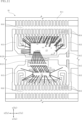
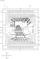
- Figures 10 to 12 are plan views showing a step in the method for manufacturing electronic device A1.
- the lead frame 81 is a plate-shaped material.
- the base material of the lead frame 81 is made of copper.
- the lead frame 81 may be formed by performing an etching process or the like on a metal plate, or may be formed by performing a punching process on a metal plate.
- the lead frame 81 has a main surface 81A and a back surface 81B that are separated in the thickness direction z.
- the lead frame 81 includes an outer frame 811, a first die pad 812A, a second die pad 812B, a plurality of first leads 813, a plurality of second leads 814, a plurality of support leads 815, a dam bar 816, and a plurality of extensions 817.
- the outer frame 811 and the dam bar 816 do not constitute the electronic device A1.
- the first die pad 812A is a portion that will later become the first die pad 21A.
- the second die pad 812B is a portion that will later become the second die pad 21B.
- the first leads 813 are portions that will later become the first lead terminals 22.
- the second leads 814 are portions that will later become the second lead terminals 23.
- the support leads 815 are portions that will later become the first lead portion 221 of the first terminal 22A at one end, the second lead portion 231 of the second terminal 23A at one end, the lead portion 224 of the first terminal 22B at the other end, and the lead portion 234 of the second terminal 23B at the other end.
- the extensions 817 are portions that will later become the first extension portion 223 of the first terminal 22A at one end, and the second extension portion 233 of the second terminal 23A at one end.
- the first semiconductor element 11 and the insulating element 12 are bonded to the first die pad 812A by die bonding, and the second semiconductor element 13 is bonded to the second die pad 812B by die bonding.
- each of the multiple wires 31 to 34 is formed by wire bonding.
- the sealing resin 5 is formed.
- the sealing resin 5 is formed by transfer molding.
- the lead frame 81 is housed in a mold having multiple cavities.
- the part of the lead frame 81 that is the conductive support member 2 covered with the sealing resin 5 in the electronic device A1 is housed in one of the multiple cavities.
- the fluidized resin is poured from the pot through the runner into each of the multiple cavities.
- the lead frame 81 is provided with a first gate 891 and a second gate 892.
- the first gate 891 is an inlet for the fluidized resin.
- the second gate 892 is an outlet for the fluidized resin.
- the resin burrs located outside each of the multiple cavities 88 are removed with high-pressure water or the like. At this time, when the resin burrs located at the first gate 891 are removed, a first gate mark 591 is formed in the sealing resin 5. Similarly, when the resin burr located at the second gate 892 is removed, a second gate mark 592 is formed in the sealing resin 5. This completes the formation of the sealing resin 5.
- the electronic device A1 is manufactured.
- the electronic device A1 includes a conductive support member 2, a plurality of electronic elements 1 arranged on the z1 side of the conductive support member 2 in the thickness direction z, and a sealing resin 5.
- the sealing resin 5 covers the plurality of electronic elements 1 and a part of the conductive support member 2.
- the sealing resin 5 has a first resin side surface 53 facing the x1 side of the first direction x, and a first gate mark 591 having a rougher surface than other areas of the first resin side surface 53 is formed on the first resin side surface 53.
- the one-end first terminal 22A (one of the multiple first lead terminals 22 constituting the conductive support member 2) has a first extension portion 223, and the one-end second terminal 23A (one of the multiple second lead terminals 23 constituting the conductive support member 2) has a second extension portion 233.
- the first extension portion 223 and the second extension portion 233 are located closest to the first gate mark 591 in the first direction x of the conductive support member 2.
- the first extension portion 223 and the second extension portion 233 include a portion (first portion) located inward from the first gate mark 591 in the second direction y when viewed in the thickness direction z.
- the resin collides with the portions (first portions) of the first extension portion 223 and the second extension portion 233, reducing the flow rate of the fluidized resin and making it difficult to draw in air. Therefore, it is possible to suppress the occurrence of pinholes (voids) due to air entrainment, and to suppress poor filling of the sealing resin 5.
- the distance (first distance D1) in the first direction x between the first gate mark 591 and the portion (first portion) of the first extension portion 223 and the second extension portion 233 that is located inward from the first gate mark 591 in the second direction y is greater than 0 mm and is equal to or less than 2.4 mm.
- the length of the first gate mark 591 in the second direction y (second dimension L2) and the first distance D1 have a relationship in which as one becomes relatively larger, the other becomes relatively smaller.
- the product of the length of the first gate mark 591 in the second direction y (second dimension L2) and the first distance D1 is 0.21 to 5.0 mm 2.
- the ratio of the length in the second direction y (third dimension L3) of the portion (first portion) of the first extension portion 223 and the second extension portion 233 located inward from the first gate mark 591 in the second direction y to the length in the second direction y (second dimension L2) of the first gate mark 591 is 50 to 100%.
- the ratio of the first distance D1 to the second dimension L2 is greater than 0% and less than 50%.
- the ratio of the first distance D1 to the dimension in the thickness direction z between the resin main surface 51 and the resin back surface 52 (fourth dimension L4) is greater than 0% and less than 70%.
- the electronic elements 1 include a first semiconductor element 11 (first electronic element), a second semiconductor element 13 (second electronic element), and an insulating element 12.
- the first semiconductor element 11 forms a first circuit together with the first die pad 21A
- the second semiconductor element 13 forms a second circuit together with the second die pad 21B.
- the insulating element 12 is mounted on either the first die pad 21A or the second die pad 21B, relays the transmission and reception of signals between the first circuit and the second circuit, and insulates the first circuit and the second circuit from each other.
- the configuration of the one-end first terminal 22A and the one-end second terminal 23A differs from that of the electronic device A1 of the above embodiment.
- the first extension portion 223 is located on the x1 side in the first direction x relative to the first lead portion 221.
- the second extension portion 233 is located on the x1 side in the first direction x relative to the second lead portion 231.
- the first extension portion 223 and the second extension portion 233 are located on the x1 side in the first direction x relative to the electronic device A1 of the above embodiment.
- the first distance D1 in the first direction x between the first gate mark 591 and that portion is smaller than the first distance D1 in the electronic device A1.
- the flow speed of the fluidized resin is reduced when the resin collides with the portions (first portions) of the first extension portion 223 and the second extension portion 233, making it difficult to draw in air. Therefore, it is possible to suppress the occurrence of pinholes (voids) due to the entrapment of air, and to suppress insufficient filling of the sealing resin 5.
- the first extension 223 is located on the x1 side of the first lead 221 in the first direction x in the one end side first terminal 22A.
- the second extension 233 is located on the x1 side of the second lead 231 in the one end side second terminal 23A.
- This configuration is preferable in terms of suppressing the occurrence of pinholes in the sealing resin 5, and can further suppress filling defects of the sealing resin 5.
- the electronic device A11 has the same effects as the electronic device A1 of the above embodiment.
- the electronic device A2 includes a plurality of electronic elements 1, a conductive support member 2, a plurality of wires 41 to 46, and a sealing resin 5.
- the specific use of the electronic device A2 is not limited in any way, but may be for detecting the battery voltage of an electric vehicle, for example.
- the electronic device A2 does not detect the battery voltage of an electric vehicle, but may detect other voltages of the electric vehicle, or may detect voltages used in industrial equipment, home appliances, or power supplies other than electric vehicles.
- the electronic device A1 is a surface-mounted semiconductor package, and in this embodiment, the package format is SOP (Small Outline Package) as shown in FIGS. 1 to 8.
- electronic device A2 In the description of electronic device A2, three mutually perpendicular directions, namely, thickness direction z, first direction x, and second direction y, will be referred to as appropriate. As shown in Figures 15 and 16, electronic device A2 is rectangular (or approximately rectangular) when viewed in thickness direction z (in a plan view).
- the conductive support member 2 is a member that constitutes a conductive path between the multiple electronic elements 1 and a circuit board of an electric vehicle or the like in the electronic device A2.
- the conductive support member 2 includes metals such as copper, nickel, and iron (Fe).
- the conductive support member 2 includes a die pad portion 21, multiple first lead terminals 25, and multiple second lead terminals 26.
- the conductive support member 2 is obtained from the same lead frame.
- the conductive support member 2 is formed, for example, by subjecting a metal plate material to a process selected from punching, bending, etching, and the like.
- a plating layer made of silver, nickel, gold, or the like may be provided at appropriate locations of each of the conductive support members 2 (the die pad portion 21, multiple first lead terminals 25, and multiple second lead terminals 26) as necessary.
- the die pad portion 21 supports a plurality of electronic elements 1.
- the die pad portion 21 has a first die pad 21A and a second die pad 21B.
- the first die pad 21A is disposed on the y1 side of the second direction y.
- the second die pad 21B is disposed on the y2 side of the second direction y.
- the first die pad 21A and the second die pad 21B are spaced apart from each other in the second direction y.
- the die pad portion 21 (each of the first die pad 21A and the second die pad 21B) has a mounting surface 211 facing the z1 side of the thickness direction z.
- the multiple first lead terminals 25 are components that are joined to a circuit board of an electric vehicle or the like to form a conductive path between the electronic device A1 and the circuit board. As shown in Figures 15, 16, and 18, the multiple first lead terminals 25 are arranged at intervals from each other in the first direction x. The multiple first lead terminals 25 are exposed so as to extend from the sealing resin 5 (third resin side surface 55 described below) toward the y1 side in the second direction y.
- the multiple first lead terminals 25 include one end side first terminal 25A, the other end side first terminal 25B, and multiple intermediate first terminals 26C.
- the one-end first terminal 25A is located at the end of the multiple first lead terminals 25 on the x1 side in the first direction x. As shown in FIG. 16, the one-end first terminal 25A has a terminal portion 251 and a lead portion 252.
- the terminal portion 251 is a portion of the first terminal 25A on one end side that is exposed from the sealing resin 5.
- the terminal portion 251 protrudes from the sealing resin 5 to the y1 side in the second direction y.
- the terminal portion 251 has a rectangular shape with the second direction y as its longitudinal direction.
- the terminal portion 251 is bent in a gull-wing shape when viewed in the first direction x.
- the tip portion of the terminal portion 251 is a portion that is joined to a circuit board when the electronic device A2 is mounted on the circuit board of an electric vehicle or the like.
- the lead portion 252 is a portion of the first terminal 25A on one end side that is covered with the sealing resin 5.
- the lead portion 252 is connected to the terminal portion 251 and extends from the terminal portion 251 inwardly into the sealing resin 5.
- the lead portion 252 is appropriately bent in a plan view and includes a portion extending in the second direction y, a portion extending in the first direction x, and a portion connected to the two portions and extending in a direction inclined with respect to the second direction y and the first direction x.
- the end of the lead portion 252 opposite the terminal portion 251 is connected to the first die pad 21A.
- the other end first terminal 25B is located at the end of the multiple first lead terminals 25 on the x2 side in the first direction x. As shown in FIG. 16, the other end first terminal 25B has a terminal portion 254 and a lead portion 255.
- the terminal portion 254 is a portion of the other end side first terminal 25B that is exposed from the sealing resin 5.
- the terminal portion 254 protrudes from the sealing resin 5 to the y1 side in the second direction y.
- the terminal portion 254 has a rectangular shape with the second direction y as its longitudinal direction. As shown in FIG. 19, the terminal portion 254 is bent in a gull-wing shape when viewed in the first direction x.
- the tip portion of the terminal portion 254 is a portion that is joined to a circuit board when the electronic device A2 is mounted on the circuit board of an electric vehicle or the like.
- the lead portion 255 is the portion of the other end side first terminal 25B that is covered with the sealing resin 5.
- the lead portion 255 is connected to the terminal portion 254 and extends from the terminal portion 254 inwardly into the sealing resin 5.
- the end of the lead portion 255 opposite the terminal portion 254 is connected to the first die pad 21A.
- the multiple intermediate first terminals 25C are arranged between the one end side first terminal 25A and the other end side first terminal 25B, as shown in Figures 16 and 18.
- Each of the multiple intermediate first terminals 25C includes a terminal portion 256 and a lead portion 257, as shown in Figure 16.
- the electronic device A2 has multiple terminal portions 256 and multiple lead portions 257.
- the terminal portions 256 and lead portions 257 described below are common to each intermediate first terminal 25C, unless otherwise specified.
- the terminal portion 256 is a portion of each intermediate first terminal 25C that is exposed from the sealing resin 5.
- Each terminal portion 254 protrudes from the sealing resin 5 toward the y1 side in the second direction y.
- each terminal portion 256 is strip-shaped with the second direction y as its longitudinal direction.
- the multiple terminal portions 256 are arranged at equal intervals along the first direction x. As shown in FIG. 21 etc., each terminal portion 256 is bent in a gull-wing shape when viewed in the first direction x.
- the multiple terminal portions 256 overlap each other when viewed in the first direction x.
- the tip portion of each terminal portion 256 is a portion that is joined to a circuit board when the electronic device A2 is mounted on the circuit board of an electric vehicle or the like.
- the lead portion 257 is the portion of each intermediate first terminal 25C that is covered with the sealing resin 5.
- the lead portion 257 is connected to the terminal portion 256 and extends from the terminal portion 256 inwardly into the sealing resin 5.
- the multiple second lead terminals 26 are components that are joined to a circuit board of an electric vehicle or the like to form a conductive path between the electronic device A1 and the circuit board. As shown in Figures 15, 16, and 20, the multiple second lead terminals 26 are arranged at intervals in the first direction x. The multiple second lead terminals 26 are exposed so as to extend from the sealing resin 5 (the fourth resin side surface 56 described below) toward the y2 side in the second direction y.
- the multiple second lead terminals 26 include one end side second terminal 26A and the other end side second terminal 26B.
- the one-end second terminal 26A is located at the end of the multiple second lead terminals 26 on the x1 side in the first direction x. As shown in FIG. 16, the one-end second terminal 26A has a terminal portion 261 and a lead portion 262.
- the terminal portion 261 is a portion of the one-end second terminal 26A that is exposed from the sealing resin 5.
- the terminal portion 261 protrudes from the sealing resin 5 to the y2 side in the second direction y.
- the terminal portion 261 has a rectangular shape with the second direction y as its longitudinal direction.
- the terminal portion 261 is bent in a gull-wing shape when viewed in the first direction x.
- the tip portion of the terminal portion 261 is a portion that is joined to a circuit board when the electronic device A2 is mounted on the circuit board of an electric vehicle or the like.
- the lead portion 262 is a portion of the one-end second terminal 26A that is covered with the sealing resin 5.
- the lead portion 262 is connected to the terminal portion 261 and extends from the terminal portion 261 inwardly into the sealing resin 5.
- the lead portion 262 is appropriately bent in a plan view, and includes a portion that extends in the second direction y and a portion that extends in the first direction x.
- the other end side second terminal 26B is located at the end of the multiple second lead terminals 26 on the x2 side in the first direction x. As shown in FIG. 16, the other end side second terminal 26B has a terminal portion 264 and a lead portion 265.
- the terminal portion 264 is a portion of the other end side second terminal 26B that is exposed from the sealing resin 5.
- the terminal portion 264 protrudes from the sealing resin 5 to the y2 side in the second direction y.
- the terminal portion 264 has a rectangular shape with the second direction y as its longitudinal direction. As shown in FIG. 19, the terminal portion 264 is bent in a gull-wing shape when viewed in the first direction x.
- the tip portion of the terminal portion 264 is a portion that is joined to a circuit board when the electronic device A2 is mounted on the circuit board of an electric vehicle or the like.
- the lead portion 265 is a portion of the other end side second terminal 26B that is covered with the sealing resin 5.
- the lead portion 265 is connected to the terminal portion 264 and extends from the terminal portion 264 inwardly into the sealing resin 5.
- the end of the lead portion 265 opposite the terminal portion 264 is connected to the second die pad 21B.
- the shapes and positional relationships of the conductive support member 2 are not limited to the example shown in the figure, and can be changed as appropriate depending on the specifications of electronic device A2.
- the multiple electronic elements 1 are elements that perform electrical functions in the electronic device A2. Although the specific functions of the multiple electronic elements 1 are not limited in any way, in this embodiment, the multiple electronic elements 1 have a function of detecting voltage. In the illustrated example, the multiple electronic elements 1 include a first electronic element 14 and a second electronic element 15 that are separated from each other.
- the second electronic element 15 is mounted on the mounting surface 211 of the second die pad 21B.
- the second electronic element 15 outputs to the first electronic element 14 a first signal corresponding to the potential of the other end side second terminal 26B and a second signal corresponding to the potential of the one end side second terminal 26A.
- the second electronic element 15 has a plurality of electrodes 151, 152, 153 arranged on its upper surface in the thickness direction z.
- the first electronic element 14 is mounted on the first die pad 21A.
- the first electronic element 14 receives the first and second signals from the second electronic element 15, and outputs a third signal according to the potential difference between the other end second terminal 26B and the one end second terminal 26A.
- the first electronic element 14 outputs a detection signal (third signal) of the voltage applied between the other end second terminal 26B and the one end second terminal 26A.
- the first electronic element 14 has multiple electrodes 141, 142 arranged on its upper surface in the thickness direction z.
- the multiple electronic elements 1 (first electronic element 14 and second electronic element 15) have a circuit configuration, for example, as shown in FIG. 23.
- the second electronic element 15 includes multiple resistive elements R1 to R4, and the first electronic element 14 includes an operational amplifier OP and a resistive element R5.
- the circuit configuration of the multiple electronic elements 1 is not limited to the example shown in FIG. 23.
- the two resistive elements R1 and R2 are connected in series with each other.
- the two resistive elements R1 and R2 divide the voltage of terminal T1 (the potential difference between the potential of terminal T1 and the reference potential of ground GND).
- terminal T1 corresponds to each electrode 152.
- the connection point of the two resistive elements R1 and R2 is connected to the non-inverting input terminal of the operational amplifier OP.
- the two resistive elements R3 and R4 are connected in series with each other.
- the two resistive elements R3 and R4 divide the voltage of terminal T2 (the potential difference between the potential of terminal T2 and the reference potential of ground GND).
- terminal T2 corresponds to each electrode 151.
- connection point of the two resistive elements R3 and R4 is connected to the inverting input terminal of the operational amplifier OP.
- electronic device A2 detects the voltage of a battery installed in an electric vehicle, one of terminals T1 and T2 is electrically connected to the high-potential terminal of the battery, and the other is electrically connected to the low-potential terminal.
- the operational amplifier OP receives a first signal (in this embodiment, a signal obtained by dividing the voltage at terminal T1) corresponding to the potential at terminal T1 and a second signal (in this embodiment, a signal obtained by dividing the voltage at terminal T2) corresponding to the potential at terminal T2, and outputs a third signal corresponding to the potential difference between terminals T1 and T2.
- the resistive element R5 is an element (feedback resistor) for determining the amplification gain of the operational amplifier OP, and one end of the resistive element R5 is connected to the inverting input terminal of the operational amplifier OP, and the other end is connected to the output terminal of the operational amplifier OP.
- the first electronic element 14 does not have to include the resistive element R5.
- the multiple wires 41 to 46 each electrically connect parts spaced apart from one another.
- the multiple wires 41 to 46 each are bonding wires.
- the multiple wires 41 to 46 each contain, for example, gold, aluminum, or copper.
- the wire 41 is joined to the electrode 151 and the lead portion 265 of the second electronic element 15, and electrically connects the second electronic element 15 to the other end side second terminal 26B.
- the terminal portion 264 of the other end side second terminal 26B is electrically connected to the second electronic element 15 via the wire 41.
- the wire 42 is joined to the electrode 152 and the lead portion 262 of the second electronic element 15, and electrically connects the second electronic element 15 to the one-end second terminal 26A.
- the terminal portion 261 of the one-end second terminal 26A is electrically connected to the second electronic element 15 via the wire 42.
- each of the multiple wires 43 is joined to the electrode 141 of the first electronic element 14 and one of the multiple lead portions 257, electrically connecting the first electronic element 14 to one of the multiple intermediate first terminals 25C.
- each terminal portion 256 of the multiple intermediate first terminals 25C is electrically connected to the first electronic element 14 via one of the multiple wires 43.
- the wire 44 is joined to the electrode 141 of the first electronic element 14 and the lead portion 255, and electrically connects the first electronic element 14 to the other end side first terminal 25B.
- the terminal portion 254 of the other end side first terminal 25B is electrically connected to the first electronic element 14 via the wire 44.
- the wire 45 is joined to the electrode 141 and the lead portion 252 of the first electronic element 14, and electrically connects the first electronic element 14 and the one-end first terminal 25A.
- the terminal portion 251 of the one-end first terminal 25A is electrically connected to the first electronic element 14 via the wire 45.
- the multiple wires 46 are joined to the electrode 153 of the second electronic element 15 and the electrode 142 of the first electronic element 14, electrically connecting the second electronic element 15 and the first electronic element 14.
- the multiple wires 46 are transmission paths for the first signal and the second signal.
- the sealing resin 5 covers the die pad portion 21 (first die pad 21A and second die pad 21B), a portion of each of the first lead terminals 22 and the second lead terminals 23, the electronic elements 1 (first electronic element 14 and second electronic element 15), and the wires 41 to 46.
- the sealing resin 5 contains an insulating material such as an epoxy resin.
- the sealing resin 5 is made of a resin material having a CTI (Comparative Tracking Index) of 600 V or more.
- the sealing resin 5 has a rectangular parallelepiped shape, for example.
- the sealing resin 5 has a dimension along the first direction x of, for example, 5 mm to 15 mm, and a dimension along the second direction y of, for example, 3 mm to 13 mm.
- the sealing resin 5 has a resin main surface 51, a resin back surface 52, a first resin side surface 53, a second resin side surface 54, a third resin side surface 55, and a fourth resin side surface 56.
- the resin main surface 51 and the resin back surface 52 are located apart from each other in the thickness direction z.
- the resin main surface 51 and the resin back surface 52 face opposite each other in the thickness direction z.
- the resin main surface 51 faces the z1 side in the thickness direction z
- the resin back surface 52 faces the z2 side in the thickness direction z.
- Each of the resin main surface 51 and the resin back surface 52 is flat (or approximately flat).
- the first resin side surface 53, the second resin side surface 54, the third resin side surface 55, and the fourth resin side surface 56 are each connected to the resin main surface 51 and the resin back surface 52, and are sandwiched between the resin main surface 51 and the resin back surface 52 in the thickness direction z.
- the first resin side surface 53 is located on the x1 side of the first direction x and faces the x1 side of the first direction x.
- the second resin side surface 54 is located on the x2 side of the first direction x and faces the x2 side of the first direction x.
- the third resin side surface 55 and the fourth resin side surface 56 are located apart from each other in the second direction y, and are connected to the first resin side surface 53 and the second resin side surface 54. As shown in FIGS. 15, 17, and 19, the third resin side surface 55 is located on the y1 side of the second direction y and faces the y1 side of the second direction y. A portion of each of the multiple first lead terminals 22 protrudes from the third resin side surface 55.
- the fourth resin side surface 56 is located on the y2 side of the second direction y and faces the y2 side of the second direction y. A portion of each of the multiple second lead terminals 23 protrudes from the fourth resin side surface 56.
- a first gate mark 591 is formed on the first resin side surface 53.
- the first gate mark 591 has a rougher surface than other areas of the first resin side surface 53 excluding the first gate mark 591.
- the first gate mark 591 appears by cutting the sealing resin 5 at the first gate 891, similar to the process of forming the sealing resin 5 (see FIG. 12) in the manufacturing process of the electronic device A1 described above.
- the first gate mark 591 is located slightly shifted toward the y2 side in the second direction y from the center in the second direction y of the first resin side surface 53.
- the lead portion 262 of the one-end second terminal 26A includes an inner portion 262a, which is a portion located inward from the first gate mark 591 in the second direction y when viewed in the thickness direction z.
- the inner portion 262a is the portion of the conductive support member 2 located closest to the first gate mark 591 in the first direction x.
- This inner portion 262a corresponds to an example of the "first portion" of the present disclosure.
- the inner portion 262a is hatched.
- the inner portion 262a (first portion) overlaps with the first gate mark 591 when viewed in the first direction x.
- the entire inner portion 262a overlaps with the first gate mark 591 when viewed in the first direction x.
- the first gate mark 591 and the inner portion 262a satisfy the following relationship.
- the ratio of the first distance D1 to the first dimension L1 is, for example, in the range of more than 0% to less than 500%, and preferably in the range of 40 to 200%.
- a specific value of the first distance D1 is, for example, more than 0 mm to less than 2.4 mm, and preferably 0.21 to 1.0 mm.
- the first distance D1 is about 0.35 mm.
- the first dimension L1 is about 0.5 mm.
- the length of the first gate mark 591 in the second direction y (second dimension L2) and the first distance D1 are in a relationship such that as one becomes relatively large, the other becomes relatively small (see FIG. 17).
- the second dimension L2 is, for example, about 1.0 to 5.0 mm, and the product of the second dimension L2 and the first distance D1 is 0.21 to 5.0 mm2 . In the example illustrated in this embodiment, the second dimension L2 is about 3.0 mm.
- the ratio of the area (area S2) of the portion of the inner part 262a (first part) that overlaps with the first gate mark 591 to the area (area S1) of the first gate mark 591 is greater than 0% and is not greater than 50% (see FIG. 17).
- the ratio of the area S2 of the portion of the inner part 262a that overlaps with the first gate mark 591 to the area S1 of the first gate mark 591 is approximately 15%.
- the ratio of the length in the second direction y (third dimension L3) of the inner portion 262a (first portion) to the second dimension L2 is 50 to 100% (see FIG. 17).
- the ratio of the first distance D1 to the second dimension L2 is greater than 0% and equal to or less than 50% (see FIG. 16 and FIG. 17).
- the third dimension L3 is approximately 1.5 mm.
- the ratio of the first distance D1 to the dimension (fourth dimension L4) in the thickness direction z between the resin main surface 51 and the resin back surface 52 is greater than 0% and is not greater than 70% (see Figures 16 and 17).
- a second gate mark 592 is formed on the second resin side surface 54.
- the second gate mark 592 has a rougher surface than other areas of the second resin side surface 54 excluding the second gate mark 592.
- the second gate mark 592 appears when the sealing resin 5 is cut at the second gate 892 in the process of forming the sealing resin 5 (see FIG. 12) in the manufacturing process of the electronic device A1 described above.
- the second gate mark 592 is located slightly shifted toward the y2 side in the second direction y from the center in the second direction y of the second resin side surface 54.
- the electronic device A2 includes a conductive support member 2, a plurality of electronic elements 1 arranged on the z1 side of the conductive support member 2 in the thickness direction z, and a sealing resin 5.
- the sealing resin 5 covers the plurality of electronic elements 1 and a part of the conductive support member 2.
- the sealing resin 5 has a first resin side surface 53 facing the x1 side of the first direction x, and a first gate mark 591 having a rougher surface than other areas of the first resin side surface 53 is formed on the first resin side surface 53.
- the one-end second terminal 26A (one of the plurality of second lead terminals 26 constituting the conductive support member 2) has a lead portion 262.
- the lead portion 262 includes an inner portion 262a (first portion) that is a portion located inward from the first gate mark 591 in the second direction y when viewed in the thickness direction z.
- the inner portion 262a is located closest to the first gate mark 591 in the first direction x of the conductive support member 2.
- the ratio of the first distance D1 to the first dimension L1 is greater than 0% and less than or equal to 500%.
- the inner part 262a (first part), which is a part of the lead part 262 located inside the first gate mark 591 in the second direction y, is located relatively close to the first gate mark 591.
- the inner part 262a (first part), which is located inside the first gate mark 591 in the second direction y, is located relatively close to the first gate mark 591 as described above.
- the distance (first distance D1) between the first gate mark 591 and the inner portion 262a (first portion) in the first direction x is greater than 0 mm and is equal to or less than 2.4 mm.
- the length of the first gate mark 591 in the second direction y (second dimension L2) and the first distance D1 are in a relationship such that as one becomes relatively larger, the other becomes relatively smaller.
- the product of the length of the first gate mark 591 in the second direction y (second dimension L2) and the first distance D1 is 0.21 to 5.0 mm2 .
- the inner portion 262a (first portion) overlaps with the first gate mark 591.
- the ratio of the area (area S2) of the portion of the inner portion 262a (first portion) overlapping with the first gate mark 591 to the area (area S1) of the first gate mark 591 is greater than 0% and less than or equal to 50%.
- the ratio of the length in the second direction y of the inner portion 262a (first portion) (third dimension L3) to the length in the second direction y of the first gate mark 591 (second dimension L2) is 50 to 100%.
- the ratio of the first distance D1 to the second dimension L2 is greater than 0% and less than 50%.
- the ratio of the first distance D1 to the dimension in the thickness direction z between the resin main surface 51 and the resin back surface 52 (fourth dimension L4) is greater than 0% and less than 70%.
- Fig. 24 shows an electronic device according to a first modified example of the first embodiment.
- Fig. 24 is a plan view showing an electronic device A21 of this modified example.
- the sealing resin 5 is seen through.
- the seen-through sealing resin 5 is shown by imaginary lines.
- elements that are the same as or similar to those of the electronic device A2 of the above embodiment are given the same reference numerals as in the above embodiment, and descriptions thereof will be omitted as appropriate.
- the arrangement and specific shapes of the die pad portion 21 (first die pad 21A and second die pad 21B), the multiple first lead terminals 25, and the multiple second lead terminals 26 are different from those of the electronic device A2 of the above embodiment.
- die pad portion 21 (first die pad 21A and second die pad 21B) is located on the x1 side in the first direction x compared to electronic device A2 described above.
- the ends of first die pad 21A and second die pad 21B on the x1 side in the first direction x are located closest to first gate mark 591 in the first direction x of conductive support member 2.
- the lead portion 252 extends in the second direction y.
- the lead portion 252 is rectangular with the second direction y as its longitudinal direction.
- the end of the lead portion 252 opposite the terminal portion 251 is connected to the first die pad 21A.
- the lead portion 262 extends in the second direction y.
- the lead portion 262 is rectangular with the second direction y as its longitudinal direction.
- the end of the lead portion 262 opposite the terminal portion 261 is connected to the second die pad 21B.
- the first die pad 21A includes an inner portion 213, which is a portion located inward from the first gate mark 591 in the second direction y when viewed in the thickness direction z.
- the second die pad 21B includes an inner portion 214, which is a portion located inward from the first gate mark 591 in the second direction y when viewed in the thickness direction z.
- the inner portions 213 and 214 are located closest to the first gate mark 591 in the first direction x of the conductive support member 2.
- the inner portions 213 and 214 correspond to an example of a "first portion" in this disclosure. In FIG. 24, the inner portions 213 and 214 are hatched.
- the inner parts 213, 214 (first parts) of the first die pad 21A and the second die pad 21B which are parts located inward from the first gate mark 591 in the second direction y, are located relatively close to the first gate mark 591.
- the inner parts 213, 214 (first parts) of the first die pad 21A and the second die pad 21B which are located inward from the first gate mark 591 in the second direction y, are located relatively close to the first gate mark 591 as described above.
- the flow speed of the fluidized resin is reduced when the resin collides with the inner parts 213, 214 (first parts), making it difficult to draw in air. Therefore, it is possible to suppress the occurrence of pinholes (voids) due to the entrapment of air, and to suppress insufficient filling of the sealing resin 5.
- the inner parts 213, 214 (first parts) of the first die pad 21A and the second die pad 21B located inside the first gate mark 591 in the second direction y are arranged relatively close to the first gate mark 591, so that the resin collides with the inner parts 213, 214 (first parts), which breaks down the air entrapped in the resin, thereby suppressing the occurrence of pinholes.
- the electronic device A21 has the same effects as the electronic device A2 of the above embodiment.
- the electronic device according to the present disclosure is not limited to the above-described embodiment.
- the specific configuration of each part of the electronic device according to the present disclosure can be freely designed in various ways.
- Appendix 1 A conductive support member; At least one electronic element disposed on one side of the conductive support member in a thickness direction; a sealing resin that covers the at least one electronic element and a portion of the conductive support member, the sealing resin has a first resin side surface facing one side in a first direction perpendicular to the thickness direction, a first gate mark having a surface rougher than other regions of the first resin side surface is formed on the first resin side surface, the conductive support member includes a first portion that is located closest to the first gate mark in the first direction and is located inward of the first gate mark in a second direction perpendicular to the thickness direction and the first direction when viewed in the thickness direction, An electronic device, wherein a ratio of a first distance, which is a distance between the first gate mark and the first portion in the first direction, to a first dimension, which is a length of the first gate mark in the thickness direction, is greater than 0% and not greater than 500%.
- Appendix 2 2. The electronic device of claim 1, wherein the first distance is greater than 0 mm and less than or equal to 2.4 mm. Appendix 3. 3. The electronic device of claim 2, wherein a product of a second dimension, which is a length of the first gate mark in the second direction, and the first distance is 0.21 to 5.0 mm 2 . Appendix 4. 4. The electronic device according to claim 1, wherein, when viewed in the first direction, the first portion overlaps with the first gate mark. Appendix 5. 5. 5. The electronic device of claim 4, wherein a ratio of an area of the first portion that overlaps with the first gate mark to an area of the first gate mark when viewed in the first direction is greater than 0% and not greater than 50%. Appendix 6.
- a ratio of a third dimension, which is the length of the first portion in the second direction, to a second dimension, which is the length of the first gate mark in the second direction, is 50 to 100%.
- Appendix 7. 3. The electronic device of claim 1, wherein a ratio of the first distance to a second dimension, which is a length of the first gate mark in the second direction, is greater than 0% and is not greater than 50%.
- Appendix 8. the sealing resin has a resin main surface facing one side in the thickness direction and a resin back surface facing the other side in the thickness direction, 8.
- the conductive support member includes a die pad portion, a plurality of first lead terminals, and a plurality of second lead terminals;
- the sealing resin has a second resin side surface facing the other side in the first direction, a third resin side surface facing one side in the second direction, and a fourth resin side surface facing the other side in the second direction,
- Each of the first lead terminals protrudes from the third resin side surface to one side in the second direction
- Each of the second lead terminals protrudes from the fourth resin side surface to the other side in the second direction
- the at least one electronic element is mounted on the die pad portion.
- the die pad portion has a first die pad arranged on one side in the second direction and a second die pad arranged on the other side in the second direction and separated from the first die pad in the second direction, 10.
- the at least one electronic element includes a first electronic element mounted on the first die pad and a second electronic element mounted on the second die pad. Appendix 11.
- the plurality of first lead terminals are arranged at intervals in the first direction and include a first end terminal located at one end in the first direction
- the second lead terminals are arranged at intervals in the first direction and include a one-end second terminal located at an end on one side in the first direction
- the electronic device described in Appendix 10 wherein the first portion is included in at least one of the one end side first terminal and the one end side second terminal.
- Appendix 12. 12 The electronic device of claim 11, wherein, when viewed in the first direction, a terminal gap provided between the one-end first terminal and the one-end second terminal in the second direction overlaps with a pad gap provided between the first die pad and the second die pad in the second direction.
- Appendix 15 The electronic device described in Appendix 14, wherein the first extension portion includes a portion located on one side of the first lead portion in the first direction.
- the conductive support member includes a plurality of second lead terminals each protruding from the fourth resin side surface to the other side in the second direction, the second lead terminals are arranged at intervals in the first direction and include a one-end second terminal located at an end on one side in the first direction, the one-end second terminal has a second lead portion, a second pad portion, and a second extending portion, the second lead portion is located on one side of the die pad portion in the first direction and extends in the second direction, the second pad portion is connected to an end portion of the second lead portion on one side in the second direction and extends to the other side in the first direction, the second extension portion is connected to an end portion of the second lead portion on one side in the second direction and extends to the one side in the second direction,
Landscapes
- Structures Or Materials For Encapsulating Or Coating Semiconductor Devices Or Solid State Devices (AREA)
Abstract
Description
図1~図9に基づき、本開示の第1実施形態に係る電子装置について説明する。本実施形態の電子装置A1は、複数の電子素子1、導電支持部材2、複数のワイヤ31~34および封止樹脂5を備える。これらのうち導電支持部材2は、ダイパッド部21、複数の第1リード端子22、および複数の第2リード端子23を含む。電子装置A1の具体的な用途等は、何ら限定されないが、たとえば電気自動車またはハイブリッド自動車などのインバータ装置の配線基板に表面実装されるものである。電子装置A1のパッケージ形式は、SOP(Small Outline Package)である。電子装置A1のパッケージ形式は、SOPに限定されない。
図13および図14は、第1実施形態の第1変形例に係る電子装置を示している。図13は、本変形例の電子装置A11を示す平面図である。図14は、図13の部分拡大図である。図13において、理解の便宜上、封止樹脂5を透過している。図13においては、透過した封止樹脂5を想像線で示している。図13以降の図面において、上記実施形態の電子装置A1と同一または類似の要素には、上記実施形態と同一の符号を付しており、適宜説明を省略する。
図15~図23に基づき、本開示の第2実施形態に係る電子装置について説明する。本実施形態の電子装置A2は、複数の電子素子1、導電支持部材2、複数のワイヤ41~46および封止樹脂5を備える。電子装置A2の具体的な用途等は、何ら限定されないが、たとえば電気自動車のバッテリ電圧を検出するためのものである。電子装置A2は、電気自動車のバッテリ電圧を検出するものではなく、電気自動車の他の電圧を検出してもよいし、電気自動車ではなく、産業機器、家電機器、あるいは、電源装置などで使用される電圧を検出してもよい。電子装置A1は、表面実装型の半導体パッケージであって、本実施形態では、図1~図8に示すように、パッケージ形式はSOP(Small Outline Package)である。
図24は、第1実施形態の第1変形例に係る電子装置を示している。図24は、本変形例の電子装置A21を示す平面図である。図24において、理解の便宜上、封止樹脂5を透過している。図24においては、透過した封止樹脂5を想像線で示している。図24において、上記実施形態の電子装置A2と同一または類似の要素には、上記実施形態と同一の符号を付しており、適宜説明を省略する。
付記1.
導電支持部材と、
前記導電支持部材の厚さ方向の一方側に配置された少なくとも1つの電子素子と、
前記少なくとも1つの電子素子、および前記導電支持部材の一部を覆う封止樹脂と、を備え、
前記封止樹脂は、前記厚さ方向に直交する第1方向の一方側を向く第1樹脂側面を有し、
前記第1樹脂側面には、当該第1樹脂側面の他の領域よりも表面が粗である第1ゲート痕が形成されており、
前記導電支持部材は、前記第1方向において前記第1ゲート痕から最も近くに位置し、且つ前記厚さ方向に見て、前記厚さ方向および前記第1方向に直交する第2方向において前記第1ゲート痕よりも内方に位置する第1部を含み、
前記第1ゲート痕の前記厚さ方向における長さである第1寸法に対する、前記第1ゲート痕と前記第1部との前記第1方向における距離である第1距離の割合は、0%を超えて500%以下である、電子装置。
付記2.
前記第1距離は、0mmを超えて2.4mm以下である、付記1に記載の電子装置。
付記3.
前記第1ゲート痕の前記第2方向における長さである第2寸法と、前記第1距離との積が、0.21~5.0mm2である、付記2に記載の電子装置。
付記4.
前記第1方向に見て、前記第1部は前記第1ゲート痕と重なる、付記1ないし3のいずれかに記載の電子装置。
付記5.
前記第1方向に見て、前記第1ゲート痕の面積に対する前記第1部の前記第1ゲート痕と重なる部分の面積の割合は、0%を超えて50%以下である、付記4に記載の電子装置。
付記6.
前記第1ゲート痕の前記第2方向における長さである第2寸法に対する、前記第1部の前記第2方向の長さである第3寸法の割合は、50~100%である、付記1ないし5のいずれかに記載の電子装置。
付記7.
前記第1ゲート痕の前記第2方向における長さである第2寸法に対する前記第1距離の割合は、0%を超えて50%以下である、付記1または2に記載の電子装置。
付記8.
前記封止樹脂は、前記厚さ方向の一方側を向く樹脂主面と、前記厚さ方向の他方側を向く樹脂裏面と、を有し、
前記樹脂主面と前記樹脂裏面との前記厚さ方向の寸法である第4寸法に対する前記第1距離の割合は、0%を超えて70%以下である、付記1ないし7のいずれかに記載の電子装置。
付記9.
前記導電支持部材は、ダイパッド部と、複数の第1リード端子と、複数の第2リード端子と、を含み、
前記封止樹脂は、前記第1方向の他方側を向く第2樹脂側面と、前記第2方向の一方側を向く第3樹脂側面と、前記第2方向の他方側を向く第4樹脂側面と、を有し、
前記複数の第1リード端子の各々は、前記第3樹脂側面から前記第2方向の一方側に突き出ており、
前記複数の第2リード端子の各々は、前記第4樹脂側面から前記第2方向の他方側に突き出ており、
前記少なくとも1つの電子素子は、前記ダイパッド部に搭載される、付記1ないし8のいずれかに記載の電子装置。
付記10.
前記ダイパッド部は、前記第2方向の一方側に配置された第1ダイパッドと、前記第2方向の他方側に配置され、且つ前記第2方向において前記第1ダイパッドと離隔する第2ダイパッドと、を有し、
前記少なくとも1つの電子素子は、前記第1ダイパッドに搭載された第1電子素子と、前記第2ダイパッドに搭載された第2電子素子と、を含む、付記9に記載の電子装置。
付記11.
前記複数の第1リード端子は、前記第1方向に間隔を隔てて配置されるとともに、前記第1方向の一方側の端に位置する一端側第1端子を含み、
前記複数の第2リード端子は、前記第1方向に間隔を隔てて配置されるとともに、前記第1方向の一方側の端に位置する一端側第2端子を含み、
前記第1部は、前記一端側第1端子および前記一端側第2端子の少なくともいずれかに含まれる、付記10に記載の電子装置。
付記12.
前記第1方向に見て、前記第2方向において前記一端側第1端子と前記一端側第2端子との間に設けられた端子隙間が、前記第2方向において前記第1ダイパッドと前記第2ダイパッドとの間に設けられたパッド隙間と重なる、付記11に記載の電子装置。
付記13.
前記第1部は、前記第1ダイパッドおよび前記第2ダイパッドに含まれる、付記10に記載の電子装置。
付記14.
導電支持部材と、
前記導電支持部材の厚さ方向の一方側に配置された少なくとも1つの電子素子と、
前記少なくとも1つの電子素子、および前記導電支持部材の一部を覆う封止樹脂と、を備え、
前記封止樹脂は、前記厚さ方向に直交する第1方向の一方側を向く第1樹脂側面と、前記第1方向の他方側を向く第2樹脂側面と、前記厚さ方向および前記第1方向に直交する第2方向の一方側を向く第3樹脂側面と、前記第2方向の他方側を向く第4樹脂側面と、を有し、
前記第1樹脂側面には、当該第1樹脂側面の他の領域よりも表面が粗である第1ゲート痕が形成されており、
前記導電支持部材は、ダイパッド部と、複数の第1リード端子と、を含み、
前記複数の第1リード端子の各々は、前記第3樹脂側面から前記第2方向の一方側に突き出ており、
前記少なくとも1つの電子素子は、前記ダイパッド部に搭載されており、
前記複数の第1リード端子は、前記第1方向に間隔を隔てて配置されるとともに、前記第1方向の一方側の端に位置する一端側第1端子を含み、
前記一端側第1端子は、第1リード部、第1パッド部、および第1延出部を有し、
前記第1リード部は、前記ダイパッド部よりも前記第1方向の一方側に位置し、且つ前記第2方向に延びており、
前記第1パッド部は、前記第1リード部の前記第2方向の他方側の端部につながり、且つ前記第1方向の他方側に延び、
前記第1延出部は、前記第1リード部の前記第2方向の他方側の端部につながり、且つ前記第2方向の他方側に延びており、
前記第1延出部は、前記厚さ方向に見て、前記第2方向において前記第1ゲート痕よりも内方に位置する部分を含む、電子装置。
付記15.
前記第1延出部は、前記第1リード部よりも前記第1方向の一方側に位置する部分を含む、付記14に記載の電子装置。
付記16.
前記導電支持部材は、各々が前記第4樹脂側面から前記第2方向の他方側に突き出る複数の第2リード端子を含み、
前記複数の第2リード端子は、前記第1方向に間隔を隔てて配置されるとともに、前記第1方向の一方側の端に位置する一端側第2端子を含み、
前記一端側第2端子は、第2リード部、第2パッド部、および第2延出部を有し、
前記第2リード部は、前記ダイパッド部よりも前記第1方向の一方側に位置し、且つ前記第2方向に延びており、
前記第2パッド部は、前記第2リード部の前記第2方向の一方側の端部につながり、且つ前記第1方向の他方側に延び、
前記第2延出部は、前記第2リード部の前記第2方向の一方側の端部につながり、且つ前記第2方向の一方側に延びており、
前記第2延出部は、前記厚さ方向に見て、前記第2方向において前記第1ゲート痕よりも内方に位置する部分を含み、且つ前記第1延出部から前記第2方向の他方側に離隔する位置にある、付記14または15に記載の電子装置。
付記17.
前記第2延出部は、前記第2リード部よりも前記第1方向の一方側に位置する部分を含む、付記16に記載の電子装置。
11:第1半導体素子(第1電子素子) 111:電極
12:絶縁素子 121:第1電極
122:第2電極 13:第2半導体素子(第2電子素子)
131:電極 14:第1電子素子
141,142:電極 15:第2電子素子
151,152,153:電極 2:導電支持部材
2:半導体素子 21:ダイパッド部
21A:第1ダイパッド 21B:第2ダイパッド
211:搭載面 212:貫通孔
213,214:内方部(第1部) 22:第1リード端子
22A:一端側第1端子 22B:他端側第1端子
22C:中間第1端子 221:第1リード部
222:第1パッド部 223:第1延出部
224,226:リード部 225,227:パッド部
23:第2リード端子 23A:一端側第2端子
23B:他端側第2端子 23C:中間第2端子
231:第2リード部 232:第2パッド部
233:第2延出部 234,236:リード部
235,237:パッド部 25:第1リード端子
25A:一端側第1端子 25B:他端側第1端子
25C:中間第1端子 251,254,256:端子部
252,255,257:リード部 26:第2リード端子
26A:一端側第2端子 26B:他端側第2端子
261,264:端子部 262,265:リード部
262a:内方部2(第1部) 31~34:ワイヤ
41~46:ワイヤ 5:封止樹脂
51:樹脂主面 52:樹脂裏面
53:第1樹脂側面 531:第1上部
532:第1下部 533:第1中間部
54:第2樹脂側面 541:第2上部
542:第2下部 543:第2中間部
55:第3樹脂側面 551:第3上部
552:第3下部 553:第3中間部
56:第4樹脂側面 561:第4上部
562:第4下部 563:第4中間部
591:第1ゲート痕 592:第2ゲート痕
81:リードフレーム 81A:主面
81B:裏面 811:外枠
812A:第1ダイパッド 812B:第2ダイパッド
813:第1リード 814:第2リード
815:支持リード 816:ダムバー
817:延出部 891:第1ゲート
892:第2ゲート D1:第1距離
L1:第1寸法 L2:第2寸法
L3:第3寸法 L4:第4寸法
S1,S2:面積 OP:オペアンプ
R1~R5:抵抗素子 T1,T2:端子
Claims (17)
- 導電支持部材と、
前記導電支持部材の厚さ方向の一方側に配置された少なくとも1つの電子素子と、
前記少なくとも1つの電子素子、および前記導電支持部材の一部を覆う封止樹脂と、を備え、
前記封止樹脂は、前記厚さ方向に直交する第1方向の一方側を向く第1樹脂側面を有し、
前記第1樹脂側面には、当該第1樹脂側面の他の領域よりも表面が粗である第1ゲート痕が形成されており、
前記導電支持部材は、前記第1方向において前記第1ゲート痕から最も近くに位置し、且つ前記厚さ方向に見て、前記厚さ方向および前記第1方向に直交する第2方向において前記第1ゲート痕よりも内方に位置する第1部を含み、
前記第1ゲート痕の前記厚さ方向における長さである第1寸法に対する、前記第1ゲート痕と前記第1部との前記第1方向における距離である第1距離の割合は、0%を超えて500%以下である、電子装置。 - 前記第1距離は、0mmを超えて2.4mm以下である、請求項1に記載の電子装置。
- 前記第1ゲート痕の前記第2方向における長さである第2寸法と、前記第1距離との積が、0.21~5.0mm2である、請求項2に記載の電子装置。
- 前記第1方向に見て、前記第1部は前記第1ゲート痕と重なる、請求項1ないし3のいずれかに記載の電子装置。
- 前記第1方向に見て、前記第1ゲート痕の面積に対する前記第1部の前記第1ゲート痕と重なる部分の面積の割合は、0%を超えて50%以下である、請求項4に記載の電子装置。
- 前記第1ゲート痕の前記第2方向における長さである第2寸法に対する、前記第1部の前記第2方向の長さである第3寸法の割合は、50~100%である、請求項1ないし5のいずれかに記載の電子装置。
- 前記第1ゲート痕の前記第2方向における長さである第2寸法に対する前記第1距離の割合は、0%を超えて50%以下である、請求項1または2に記載の電子装置。
- 前記封止樹脂は、前記厚さ方向の一方側を向く樹脂主面と、前記厚さ方向の他方側を向く樹脂裏面と、を有し、
前記樹脂主面と前記樹脂裏面との前記厚さ方向の寸法である第4寸法に対する前記第1距離の割合は、0%を超えて70%以下である、請求項1ないし7のいずれかに記載の電子装置。 - 前記導電支持部材は、ダイパッド部と、複数の第1リード端子と、複数の第2リード端子と、を含み、
前記封止樹脂は、前記第1方向の他方側を向く第2樹脂側面と、前記第2方向の一方側を向く第3樹脂側面と、前記第2方向の他方側を向く第4樹脂側面と、を有し、
前記複数の第1リード端子の各々は、前記第3樹脂側面から前記第2方向の一方側に突き出ており、
前記複数の第2リード端子の各々は、前記第4樹脂側面から前記第2方向の他方側に突き出ており、
前記少なくとも1つの電子素子は、前記ダイパッド部に搭載される、請求項1ないし8のいずれかに記載の電子装置。 - 前記ダイパッド部は、前記第2方向の一方側に配置された第1ダイパッドと、前記第2方向の他方側に配置され、且つ前記第2方向において前記第1ダイパッドと離隔する第2ダイパッドと、を有し、
前記少なくとも1つの電子素子は、前記第1ダイパッドに搭載された第1電子素子と、前記第2ダイパッドに搭載された第2電子素子と、を含む、請求項9に記載の電子装置。 - 前記複数の第1リード端子は、前記第1方向に間隔を隔てて配置されるとともに、前記第1方向の一方側の端に位置する一端側第1端子を含み、
前記複数の第2リード端子は、前記第1方向に間隔を隔てて配置されるとともに、前記第1方向の一方側の端に位置する一端側第2端子を含み、
前記第1部は、前記一端側第1端子および前記一端側第2端子の少なくともいずれかに含まれる、請求項10に記載の電子装置。 - 前記第1方向に見て、前記第2方向において前記一端側第1端子と前記一端側第2端子との間に設けられた端子隙間が、前記第2方向において前記第1ダイパッドと前記第2ダイパッドとの間に設けられたパッド隙間と重なる、請求項11に記載の電子装置。
- 前記第1部は、前記第1ダイパッドおよび前記第2ダイパッドに含まれる、請求項10に記載の電子装置。
- 導電支持部材と、
前記導電支持部材の厚さ方向の一方側に配置された少なくとも1つの電子素子と、
前記少なくとも1つの電子素子、および前記導電支持部材の一部を覆う封止樹脂と、を備え、
前記封止樹脂は、前記厚さ方向に直交する第1方向の一方側を向く第1樹脂側面と、前記第1方向の他方側を向く第2樹脂側面と、前記厚さ方向および前記第1方向に直交する第2方向の一方側を向く第3樹脂側面と、前記第2方向の他方側を向く第4樹脂側面と、を有し、
前記第1樹脂側面には、当該第1樹脂側面の他の領域よりも表面が粗である第1ゲート痕が形成されており、
前記導電支持部材は、ダイパッド部と、複数の第1リード端子と、を含み、
前記複数の第1リード端子の各々は、前記第3樹脂側面から前記第2方向の一方側に突き出ており、
前記少なくとも1つの電子素子は、前記ダイパッド部に搭載されており、
前記複数の第1リード端子は、前記第1方向に間隔を隔てて配置されるとともに、前記第1方向の一方側の端に位置する一端側第1端子を含み、
前記一端側第1端子は、第1リード部、第1パッド部、および第1延出部を有し、
前記第1リード部は、前記ダイパッド部よりも前記第1方向の一方側に位置し、且つ前記第2方向に延びており、
前記第1パッド部は、前記第1リード部の前記第2方向の他方側の端部につながり、且つ前記第1方向の他方側に延び、
前記第1延出部は、前記第1リード部の前記第2方向の他方側の端部につながり、且つ前記第2方向の他方側に延びており、
前記第1延出部は、前記厚さ方向に見て、前記第2方向において前記第1ゲート痕よりも内方に位置する部分を含む、電子装置。 - 前記第1延出部は、前記第1リード部よりも前記第1方向の一方側に位置する部分を含む、請求項14に記載の電子装置。
- 前記導電支持部材は、各々が前記第4樹脂側面から前記第2方向の他方側に突き出る複数の第2リード端子を含み、
前記複数の第2リード端子は、前記第1方向に間隔を隔てて配置されるとともに、前記第1方向の一方側の端に位置する一端側第2端子を含み、
前記一端側第2端子は、第2リード部、第2パッド部、および第2延出部を有し、
前記第2リード部は、前記ダイパッド部よりも前記第1方向の一方側に位置し、且つ前記第2方向に延びており、
前記第2パッド部は、前記第2リード部の前記第2方向の一方側の端部につながり、且つ前記第1方向の他方側に延び、
前記第2延出部は、前記第2リード部の前記第2方向の一方側の端部につながり、且つ前記第2方向の一方側に延びており、
前記第2延出部は、前記厚さ方向に見て、前記第2方向において前記第1ゲート痕よりも内方に位置する部分を含み、且つ前記第1延出部から前記第2方向の他方側に離隔する位置にある、請求項14または15に記載の電子装置。 - 前記第2延出部は、前記第2リード部よりも前記第1方向の一方側に位置する部分を含む、請求項16に記載の電子装置。
Priority Applications (2)
| Application Number | Priority Date | Filing Date | Title |
|---|---|---|---|
| JP2025506672A JPWO2024190397A1 (ja) | 2023-03-15 | 2024-02-27 | |
| US19/322,030 US20260005087A1 (en) | 2023-03-15 | 2025-09-08 | Electronic device |
Applications Claiming Priority (2)
| Application Number | Priority Date | Filing Date | Title |
|---|---|---|---|
| JP2023040763 | 2023-03-15 | ||
| JP2023-040763 | 2023-03-15 |
Related Child Applications (1)
| Application Number | Title | Priority Date | Filing Date |
|---|---|---|---|
| US19/322,030 Continuation US20260005087A1 (en) | 2023-03-15 | 2025-09-08 | Electronic device |
Publications (1)
| Publication Number | Publication Date |
|---|---|
| WO2024190397A1 true WO2024190397A1 (ja) | 2024-09-19 |
Family
ID=92754973
Family Applications (1)
| Application Number | Title | Priority Date | Filing Date |
|---|---|---|---|
| PCT/JP2024/007012 Ceased WO2024190397A1 (ja) | 2023-03-15 | 2024-02-27 | 電子装置 |
Country Status (3)
| Country | Link |
|---|---|
| US (1) | US20260005087A1 (ja) |
| JP (1) | JPWO2024190397A1 (ja) |
| WO (1) | WO2024190397A1 (ja) |
Citations (4)
| Publication number | Priority date | Publication date | Assignee | Title |
|---|---|---|---|---|
| WO2016072012A1 (ja) * | 2014-11-07 | 2016-05-12 | 三菱電機株式会社 | 電力用半導体装置およびその製造方法 |
| WO2020012957A1 (ja) * | 2018-07-12 | 2020-01-16 | ローム株式会社 | 半導体装置 |
| JP2022046254A (ja) * | 2020-09-10 | 2022-03-23 | ローム株式会社 | 半導体装置 |
| WO2022145177A1 (ja) * | 2021-01-04 | 2022-07-07 | ローム株式会社 | 半導体装置 |
-
2024
- 2024-02-27 WO PCT/JP2024/007012 patent/WO2024190397A1/ja not_active Ceased
- 2024-02-27 JP JP2025506672A patent/JPWO2024190397A1/ja active Pending
-
2025
- 2025-09-08 US US19/322,030 patent/US20260005087A1/en active Pending
Patent Citations (4)
| Publication number | Priority date | Publication date | Assignee | Title |
|---|---|---|---|---|
| WO2016072012A1 (ja) * | 2014-11-07 | 2016-05-12 | 三菱電機株式会社 | 電力用半導体装置およびその製造方法 |
| WO2020012957A1 (ja) * | 2018-07-12 | 2020-01-16 | ローム株式会社 | 半導体装置 |
| JP2022046254A (ja) * | 2020-09-10 | 2022-03-23 | ローム株式会社 | 半導体装置 |
| WO2022145177A1 (ja) * | 2021-01-04 | 2022-07-07 | ローム株式会社 | 半導体装置 |
Also Published As
| Publication number | Publication date |
|---|---|
| US20260005087A1 (en) | 2026-01-01 |
| JPWO2024190397A1 (ja) | 2024-09-19 |
Similar Documents
| Publication | Publication Date | Title |
|---|---|---|
| JP7792472B2 (ja) | 半導体装置 | |
| US11742269B2 (en) | Semiconductor device | |
| US12159819B2 (en) | Semiconductor device | |
| US12068229B2 (en) | Semiconductor device | |
| US11923277B2 (en) | Semiconductor device | |
| JP7775228B2 (ja) | 半導体装置 | |
| US11894321B2 (en) | Semiconductor device with a transmitting insulating element | |
| CN116472610A (zh) | 半导体器件 | |
| US12616040B2 (en) | Metal layer plated to inner leads of a leadframe | |
| WO2024190397A1 (ja) | 電子装置 | |
| JP7843276B2 (ja) | 半導体装置 | |
| US20250069996A1 (en) | Semiconductor device and method for manufacturing semiconductor device | |
| US20240363606A1 (en) | Semiconductor device | |
| JP7837876B2 (ja) | 半導体装置 | |
| US12622333B2 (en) | Semiconductor device | |
| US20240030109A1 (en) | Semiconductor device | |
| JP2025124947A (ja) | 半導体装置、および、半導体装置の製造方法 | |
| WO2024257543A1 (ja) | 半導体装置 | |
| WO2024257544A1 (ja) | 半導体装置 | |
| WO2024135356A1 (ja) | 半導体装置 |
Legal Events
| Date | Code | Title | Description |
|---|---|---|---|
| 121 | Ep: the epo has been informed by wipo that ep was designated in this application |
Ref document number: 24770509 Country of ref document: EP Kind code of ref document: A1 |
|
| ENP | Entry into the national phase |
Ref document number: 2025506672 Country of ref document: JP Kind code of ref document: A |
|
| WWE | Wipo information: entry into national phase |
Ref document number: 2025506672 Country of ref document: JP |
|
| NENP | Non-entry into the national phase |
Ref country code: DE |
|
| 122 | Ep: pct application non-entry in european phase |
Ref document number: 24770509 Country of ref document: EP Kind code of ref document: A1 |