WO2024190237A1 - 光電変換素子および撮像装置 - Google Patents
光電変換素子および撮像装置 Download PDFInfo
- Publication number
- WO2024190237A1 WO2024190237A1 PCT/JP2024/004921 JP2024004921W WO2024190237A1 WO 2024190237 A1 WO2024190237 A1 WO 2024190237A1 JP 2024004921 W JP2024004921 W JP 2024004921W WO 2024190237 A1 WO2024190237 A1 WO 2024190237A1
- Authority
- WO
- WIPO (PCT)
- Prior art keywords
- layer
- photoelectric conversion
- electrode
- semiconductor material
- conversion element
- Prior art date
- Legal status (The legal status is an assumption and is not a legal conclusion. Google has not performed a legal analysis and makes no representation as to the accuracy of the status listed.)
- Ceased
Links
Images


Classifications
-
- H—ELECTRICITY
- H10—SEMICONDUCTOR DEVICES; ELECTRIC SOLID-STATE DEVICES NOT OTHERWISE PROVIDED FOR
- H10K—ORGANIC ELECTRIC SOLID-STATE DEVICES
- H10K30/00—Organic devices sensitive to infrared radiation, light, electromagnetic radiation of shorter wavelength or corpuscular radiation
- H10K30/80—Constructional details
- H10K30/84—Layers having high charge carrier mobility
- H10K30/86—Layers having high hole mobility, e.g. hole-transporting layers or electron-blocking layers
-
- H—ELECTRICITY
- H10—SEMICONDUCTOR DEVICES; ELECTRIC SOLID-STATE DEVICES NOT OTHERWISE PROVIDED FOR
- H10K—ORGANIC ELECTRIC SOLID-STATE DEVICES
- H10K30/00—Organic devices sensitive to infrared radiation, light, electromagnetic radiation of shorter wavelength or corpuscular radiation
- H10K30/20—Organic devices sensitive to infrared radiation, light, electromagnetic radiation of shorter wavelength or corpuscular radiation comprising organic-organic junctions, e.g. donor-acceptor junctions
-
- H—ELECTRICITY
- H10—SEMICONDUCTOR DEVICES; ELECTRIC SOLID-STATE DEVICES NOT OTHERWISE PROVIDED FOR
- H10K—ORGANIC ELECTRIC SOLID-STATE DEVICES
- H10K30/00—Organic devices sensitive to infrared radiation, light, electromagnetic radiation of shorter wavelength or corpuscular radiation
- H10K30/30—Organic devices sensitive to infrared radiation, light, electromagnetic radiation of shorter wavelength or corpuscular radiation comprising bulk heterojunctions, e.g. interpenetrating networks of donor and acceptor material domains
- H10K30/353—Organic devices sensitive to infrared radiation, light, electromagnetic radiation of shorter wavelength or corpuscular radiation comprising bulk heterojunctions, e.g. interpenetrating networks of donor and acceptor material domains comprising blocking layers, e.g. exciton blocking layers
-
- H—ELECTRICITY
- H10—SEMICONDUCTOR DEVICES; ELECTRIC SOLID-STATE DEVICES NOT OTHERWISE PROVIDED FOR
- H10K—ORGANIC ELECTRIC SOLID-STATE DEVICES
- H10K30/00—Organic devices sensitive to infrared radiation, light, electromagnetic radiation of shorter wavelength or corpuscular radiation
- H10K30/60—Organic devices sensitive to infrared radiation, light, electromagnetic radiation of shorter wavelength or corpuscular radiation in which radiation controls flow of current through the devices, e.g. photoresistors
-
- H—ELECTRICITY
- H10—SEMICONDUCTOR DEVICES; ELECTRIC SOLID-STATE DEVICES NOT OTHERWISE PROVIDED FOR
- H10K—ORGANIC ELECTRIC SOLID-STATE DEVICES
- H10K30/00—Organic devices sensitive to infrared radiation, light, electromagnetic radiation of shorter wavelength or corpuscular radiation
- H10K30/80—Constructional details
- H10K30/84—Layers having high charge carrier mobility
- H10K30/85—Layers having high electron mobility, e.g. electron-transporting layers or hole-blocking layers
-
- H—ELECTRICITY
- H10—SEMICONDUCTOR DEVICES; ELECTRIC SOLID-STATE DEVICES NOT OTHERWISE PROVIDED FOR
- H10K—ORGANIC ELECTRIC SOLID-STATE DEVICES
- H10K39/00—Integrated devices, or assemblies of multiple devices, comprising at least one organic radiation-sensitive element covered by group H10K30/00
- H10K39/30—Devices controlled by radiation
- H10K39/32—Organic image sensors
-
- H—ELECTRICITY
- H10—SEMICONDUCTOR DEVICES; ELECTRIC SOLID-STATE DEVICES NOT OTHERWISE PROVIDED FOR
- H10K—ORGANIC ELECTRIC SOLID-STATE DEVICES
- H10K85/00—Organic materials used in the body or electrodes of devices covered by this subclass
- H10K85/20—Carbon compounds, e.g. carbon nanotubes or fullerenes
-
- H—ELECTRICITY
- H10—SEMICONDUCTOR DEVICES; ELECTRIC SOLID-STATE DEVICES NOT OTHERWISE PROVIDED FOR
- H10K—ORGANIC ELECTRIC SOLID-STATE DEVICES
- H10K85/00—Organic materials used in the body or electrodes of devices covered by this subclass
- H10K85/60—Organic compounds having low molecular weight
-
- H—ELECTRICITY
- H10—SEMICONDUCTOR DEVICES; ELECTRIC SOLID-STATE DEVICES NOT OTHERWISE PROVIDED FOR
- H10K—ORGANIC ELECTRIC SOLID-STATE DEVICES
- H10K2101/00—Properties of the organic materials covered by group H10K85/00
- H10K2101/40—Interrelation of parameters between multiple constituent active layers or sublayers, e.g. HOMO values in adjacent layers
Definitions
- This disclosure relates to a photoelectric conversion element and an imaging device.
- Patent Document 1 discloses a photoelectric conversion element that has an electron blocking layer or hole blocking layer between the thin film of photoelectric conversion material and the electrode to prevent backflow of charges from the electrode.
- Patent Document 2 discloses a method of changing the bias voltage applied to electrodes connected to both ends of the photoelectric conversion element.
- the present disclosure therefore aims to provide a photoelectric conversion element etc. that can reduce parasitic sensitivity.
- the photoelectric conversion element includes a photoelectric conversion layer that contains a donor semiconductor material and an acceptor semiconductor material and converts light into a signal charge, a first electrode that collects the signal charge, a second electrode that faces the first electrode across the photoelectric conversion layer, and a charge injection layer located between the second electrode and the photoelectric conversion layer.
- the charge injection layer includes a first layer and a second layer that is stacked on the first layer.
- the ionization potential of the first layer is greater than the ionization potential of the second layer.
- the electron affinity of the first layer is greater than the electron affinity of the second layer.
- the difference between the electron affinity of the first layer and the ionization potential of the second layer is smaller than the difference between the electron affinity of the acceptor semiconductor material and the ionization potential of the donor semiconductor material.
- an imaging device includes the photoelectric conversion element and a charge accumulation region that is electrically connected to the first electrode and accumulates the signal charge.
- This disclosure provides a photoelectric conversion element and the like that can reduce parasitic sensitivity.
- FIG. 1 is a schematic cross-sectional view showing the configuration of a photoelectric conversion element according to an embodiment.
- FIG. 2 is an exemplary energy band diagram of a photoelectric conversion element according to an embodiment.
- FIG. 3 is an exemplary energy band diagram when a reverse bias voltage is applied in the photoelectric conversion element according to the embodiment.
- FIG. 4 is an exemplary energy band diagram when a forward bias voltage is applied in the photoelectric conversion element according to the embodiment.
- FIG. 5 is a schematic cross-sectional view showing the configuration of another photoelectric conversion element according to the embodiment.
- FIG. 6 is an exemplary energy band diagram of another photoelectric conversion element according to the embodiment.
- FIG. 7 is a diagram illustrating an example of a circuit configuration of the imaging device according to the embodiment.
- FIG. 8 is a schematic cross-sectional view showing a device structure of a pixel in an imaging device according to an embodiment.
- FIG. 9 is a diagram showing a part of a schematic circuit configuration of a pixel according to the embodiment.
- FIG. 10 is a timing chart showing an example of the voltage supplied to the upper electrode of the photoelectric conversion unit and the timing of the operation in each row of the pixel array of the imaging device according to the embodiment.
- FIG. 11 is a timing chart showing an example of an operation for adjusting the sensitivity of photoelectric conversion by a pulse duty control method in the imaging device according to the embodiment.
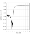
- FIG. 12 is a diagram showing current density-voltage characteristics when a bias voltage is applied to the photoelectric conversion element in the example.
- FIG. 13 is a diagram showing current density-voltage characteristics when a bias voltage is applied to the photoelectric conversion element in the comparative example.
- the photoelectric conversion element includes a photoelectric conversion layer that contains a donor semiconductor material and an acceptor semiconductor material and converts light into a signal charge, a first electrode that collects the signal charge, a second electrode that faces the first electrode across the photoelectric conversion layer, and a charge injection layer located between the second electrode and the photoelectric conversion layer.
- the charge injection layer includes a first layer and a second layer that is stacked on the first layer.
- the ionization potential of the first layer is greater than the ionization potential of the second layer.
- the electron affinity of the first layer is greater than the electron affinity of the second layer.
- the difference between the electron affinity of the first layer and the ionization potential of the second layer is smaller than the difference between the electron affinity of the acceptor semiconductor material and the ionization potential of the donor semiconductor material.
- a charge injection layer including a first layer and a second layer with such an ionization potential and electron affinity
- charge is likely to be generated at the interface between the first layer and the second layer. Therefore, when the movement of the signal charge to the first electrode is stopped and the signal charge collected by the first electrode is read out, the signal charge also remains in the photoelectric conversion layer, but among the charges generated in the charge injection layer, the charge of the opposite polarity to the signal charge moves to the first electrode side and can be recombined with the signal charge remaining in the photoelectric conversion layer.
- the photoelectric conversion element according to the second aspect of the present disclosure may be the photoelectric conversion element according to the first aspect, and the signal charge may be a hole.
- the photoelectric conversion element according to the third aspect of the present disclosure may be the photoelectric conversion element according to the second aspect, and the first layer may be located between the second layer and the photoelectric conversion layer.
- the photoelectric conversion element according to the fourth aspect of the present disclosure may be the photoelectric conversion element according to the second or third aspect, further comprising an electron blocking layer located between the first electrode and the photoelectric conversion layer.
- the photoelectric conversion element according to the fifth aspect of the present disclosure may be the photoelectric conversion element according to the first aspect, and the signal charge may be electrons.
- the photoelectric conversion element according to the sixth aspect of the present disclosure may be the photoelectric conversion element according to the fifth aspect, in which the second layer is located between the first layer and the photoelectric conversion layer.
- the photoelectric conversion element according to the seventh aspect of the present disclosure may be the photoelectric conversion element according to the fifth or sixth aspect, further comprising a hole blocking layer located between the first electrode and the photoelectric conversion layer.
- a photoelectric conversion element according to the eighth aspect of the present disclosure may be a photoelectric conversion element according to any one of the first to seventh aspects, in which the first layer contains the same material as the acceptor semiconductor material.
- a photoelectric conversion element according to a ninth aspect of the present disclosure may be a photoelectric conversion element according to any one of the first to eighth aspects, in which the second layer contains the same material as the donor semiconductor material.
- a photoelectric conversion element is a photoelectric conversion element according to any one of the first to seventh aspects, in which the photoelectric conversion layer may be a mixed film containing the donor semiconductor material and the acceptor semiconductor material, the first layer may contain the same material as the acceptor semiconductor material, and the second layer may contain the same material as the donor semiconductor material.
- the donor semiconductor material and the acceptor semiconductor material are less susceptible to stabilization than in the case of a single material film, and the difference between the electron affinity and the ionization potential increases. Therefore, even if the charge injection layer and the photoelectric conversion layer contain the same material, the difference between the electron affinity of the first layer and the ionization potential of the second layer is smaller than the difference between the electron affinity of the acceptor semiconductor material in the photoelectric conversion layer and the ionization potential of the donor semiconductor material. Therefore, a configuration having the above-mentioned relationship between electron affinity and ionization potential can be easily realized.
- an imaging device includes a photoelectric conversion element according to any one of the first to tenth aspects, and a charge accumulation region electrically connected to the first electrode and accumulating the signal charge.
- the imaging device includes the above-mentioned photoelectric conversion element, and thus parasitic sensitivity can be suppressed.
- an imaging device may be the imaging device according to the eleventh aspect, further comprising a voltage supply circuit electrically connected to the second electrode and providing a potential difference between the first electrode and the second electrode, and the voltage supply circuit may supply a first voltage to the second electrode in a first period, and supply a second voltage different from the first voltage in a second period different from the first period.
- the timing of photoelectric conversion and the timing of readout can be separated, further reducing parasitic sensitivity.
- each figure is a schematic diagram and is not necessarily an exact illustration. Therefore, for example, the scales of each figure do not necessarily match.
- the same reference numerals are used for substantially the same configuration, and duplicate explanations are omitted or simplified.
- the terms “above” and “below” do not refer to the upward direction (vertically upward) and downward direction (vertically downward) in an absolute spatial sense, but are used as terms defined by a relative positional relationship based on the stacking order in the stacked configuration. Furthermore, the terms “above” and “below” are applied not only to cases where two components are arranged with a gap between them and another component exists between the two components, but also to cases where two components are arranged closely together and are in contact with each other.
- electromagnetic waves in general including visible light, infrared light, and ultraviolet light, will be referred to as "light" for the sake of convenience.
- the photoelectric conversion element according to the present embodiment is a charge readout type photoelectric conversion element.
- the photoelectric conversion element according to the present embodiment is used in, for example, an imaging device, a photosensor, or a photodetector.
- Fig. 1 is a schematic cross-sectional view showing the configuration of a photoelectric conversion element 10 according to the present embodiment.
- the photoelectric conversion element 10 is supported on a support substrate 1, and includes a pair of electrodes, an upper electrode 7 and a lower electrode 2, a photoelectric conversion layer 4 located between the upper electrode 7 and the lower electrode 2, a charge injection layer 5 located between the upper electrode 7 and the photoelectric conversion layer 4, and an electron blocking layer 3 located between the lower electrode 2 and the photoelectric conversion layer 4.
- the upper electrode 7 is an example of a second electrode
- the lower electrode 2 is an example of a first electrode.
- the support substrate 1 may be any substrate that is commonly used to support photoelectric conversion elements, such as a glass substrate, a quartz substrate, a semiconductor substrate, or a plastic substrate.
- the lower electrode 2 collects the signal charges generated in the photoelectric conversion layer 4.
- the lower electrode 2 is formed from a metal, a metal nitride, a metal oxide, or polysilicon that has been made conductive. Examples of metals include aluminum, copper, titanium, and tungsten. An example of a method for making polysilicon conductive is doping it with impurities.
- the upper electrode 7 is disposed opposite the lower electrode 2 with the photoelectric conversion layer 4 interposed therebetween.
- the upper electrode 7 is, for example, a transparent electrode formed from a transparent conductive material.
- materials for the upper electrode 7 include transparent conductive oxide (TCO), indium tin oxide (ITO), indium zinc oxide (IZO), aluminum-doped zinc oxide (AZO), fluorine-doped tin oxide (FTO), SnO 2 , and TiO 2.
- TCO transparent conductive oxide
- ITO indium tin oxide
- IZO indium zinc oxide
- AZO aluminum-doped zinc oxide
- FTO fluorine-doped tin oxide
- SnO 2 SnO 2
- TiO 2 titanium oxide
- the upper electrode 7 may be made of a single or multiple combinations of TCO and metal materials such as aluminum (Al) and gold (Au) depending on the desired transmittance.
- the materials of the lower electrode 2 and the upper electrode 7 are not limited to the conductive materials described above, and other materials may be used.
- the lower electrode 2 may be a transparent electrode.
- the lower electrode 2 and upper electrode 7 can be produced by various methods depending on the materials used. For example, when ITO is used, methods such as electron beam method, sputtering method, resistance heating deposition method, chemical reaction method such as the sol-gel method, and application of a dispersion of indium tin oxide can be used. In this case, the lower electrode 2 and upper electrode 7 can be produced by further performing UV-ozone treatment, plasma treatment, etc. after forming the ITO film.
- the photoelectric conversion layer 4 includes a donor semiconductor material and an acceptor semiconductor material.
- the photoelectric conversion layer 4 is made of, for example, an organic semiconductor material.
- the photoelectric conversion layer 4 can be made by, for example, a wet method such as a coating method using spin coating, or a dry method such as a vacuum deposition method.
- the vacuum deposition method is a method in which the material of the layer is vaporized by heating under vacuum and deposited on the substrate.
- the charge injection layer 5 can also be made by the same method as the photoelectric conversion layer 4.
- the photoelectric conversion layer 4 is, for example, a mixed film of a bulk heterostructure containing a donor semiconductor material, such as a donor organic semiconductor material, and an acceptor semiconductor material, such as an acceptor organic semiconductor material.
- the photoelectric conversion layer 4 may have a layered structure in which a layer of a donor semiconductor material and a layer of an acceptor semiconductor material are stacked.
- the photoelectric conversion layer 4 can be easily formed as a thin film by including a donor organic semiconductor material and an acceptor organic semiconductor material. Specific examples of donor organic semiconductor materials and acceptor organic semiconductor materials are given below.
- the donor organic semiconductor material may be, for example, a triarylamine compound, a benzidine compound, a pyrazoline compound, a styrylamine compound, a hydrazone compound, a triphenylmethane compound, a carbazole compound, a polysilane compound, a thiophene compound, a phthalocyanine compound, a naphthalocyanine compound, a subphthalocyanine compound, a cyanine compound, a merocyanine compound, an oxonol compound, a polyamine compound, an indole compound, a pyrrole compound, a pyrazole compound, a polyarylene compound, a condensed aromatic carbon ring compound (for example, a naphthalene derivative, an anthracene derivative, a phenanthrene derivative, a tetracene derivative, a pyrene derivative, a perylene derivative, a fluoranthene derivative, etc.
- Acceptor organic semiconductor materials include, for example, fullerenes (e.g., C60 fullerene and C70 fullerene, etc.), fullerene derivatives (e.g., PCBM (phenyl C61 butyric acid methyl ester) and ICBA (indene C60 bisadduct), etc.), condensed aromatic carbon ring compounds (e.g., naphthalene derivatives, anthracene derivatives, phenanthrene derivatives, tetracene derivatives, pyrene derivatives, perylene derivatives, and fluoranthene derivatives, etc.), 5- to 7-membered heterocyclic compounds containing nitrogen atoms, oxygen atoms, and sulfur atoms (e.g., pyridine, pyrazine, pyrimidine, pyridazine, triazine, quinoline, quinoxaline, quinazoline, phthalazine, cinnoline, etc.), , iso
- the donor organic semiconductor material and the acceptor organic semiconductor material are not limited to the above examples.
- Low molecular weight organic compounds and high molecular weight organic compounds may be used as the donor organic semiconductor material and the acceptor organic semiconductor material that make up the photoelectric conversion layer 4, as long as they are organic compounds that can be formed into a film as a photoelectric conversion layer by either a dry method or a wet method.
- the photoelectric conversion layer 4 may also contain semiconductor materials other than those mentioned above as donor semiconductor materials and acceptor semiconductor materials.
- the photoelectric conversion layer 4 may also contain, as semiconductor materials, for example, silicon semiconductors, compound semiconductors, quantum dots, perovskite materials, carbon nanotubes, etc., or a mixture of two or more of these.
- the photoelectric conversion element 10 includes an electron blocking layer 3 provided between the lower electrode 2 and the photoelectric conversion layer 4, and a charge injection layer 5 provided between the upper electrode 7 and the photoelectric conversion layer 4.
- the electron blocking layer 3 is in contact with, for example, the lower electrode 2 and the photoelectric conversion layer 4.
- the charge injection layer 5 is in contact with, for example, the upper electrode 7 and the photoelectric conversion layer 4. Note that the photoelectric conversion element 10 does not necessarily have to include the electron blocking layer 3.
- the charge injection layer 5 has a first layer 6A and a second layer 6B stacked on the first layer 6A.
- the first layer 6A and the second layer 6B are in contact with each other.
- the first layer 6A is located between the second layer 6B and the photoelectric conversion layer 4.
- the first layer 6A is in contact with, for example, the photoelectric conversion layer 4.
- the second layer 6B is in contact with, for example, the upper electrode 7.
- FIG. 2 is an exemplary energy band diagram for the photoelectric conversion element 10 shown in FIG. 1.
- the energy band of each layer is indicated by a rectangle.
- the photoelectric conversion layer 4 When the photoelectric conversion layer 4 is irradiated with light, it generates pairs of electrons and holes inside. In the photoelectric conversion element 10, the holes in these pairs are collected by the lower electrode 2 and used as signal charges to be read out. In other words, the photoelectric conversion layer 4 converts light into signal charges.
- the signal charges may be electrons. An example in which the signal charges are electrons will be described later.
- the electron-hole pairs generated in the photoelectric conversion layer 4 are separated into electrons and holes by the electric field applied to the photoelectric conversion layer 4.
- the electrons and holes move toward the lower electrode 2 side or the upper electrode 7 side, respectively, according to the electric field.
- the semiconductor material that donates the electrons to the other material is a donor semiconductor material
- the semiconductor material that accepts the electrons is an acceptor semiconductor material.
- the photoelectric conversion layer 4 is irradiated with light, for example, the donor semiconductor material generates electron-hole pairs and donates electrons to the acceptor semiconductor material. This allows the electrons and holes to be easily separated.
- Figure 2 shows an example of energy bands when organic semiconductor materials are used as donor and acceptor semiconductor materials.
- which one is the donor semiconductor material and which one is the acceptor semiconductor material is generally determined by the relative positions of the HOMO (Highest-Occupied-Molecular-Orbital) and LUMO (Lowest-Unoccupied-Molecular-Orbital) energy levels of the two organic semiconductor materials at the contact interface.
- the upper end of the rectangle showing the energy bands is the LUMO energy level
- the lower end is the HOMO energy level.
- the energy difference between the vacuum level and the HOMO energy level is called the ionization potential.
- the energy difference between the vacuum level and the LUMO energy level is called the electron affinity.
- the semiconductor material contained in the photoelectric conversion layer 4 is an inorganic semiconductor material, the HOMO and LUMO are interpreted as the valence band and conduction band, respectively.
- the one with the smaller LUMO energy level i.e., the smaller electron affinity
- the one with the larger LUMO energy level i.e., the larger electron affinity
- the acceptor organic semiconductor material 4B the energy bands of the donor organic semiconductor material 4A and the acceptor organic semiconductor material 4B are shown slightly shifted horizontally, but this is for ease of viewing and does not indicate the distribution of the donor organic semiconductor material 4A and the acceptor organic semiconductor material 4B in the photoelectric conversion layer 4.
- the electron blocking layer 3 is provided to reduce dark current caused by electrons injected from the lower electrode 2, and suppresses the injection of electrons from the lower electrode 2 into the photoelectric conversion layer 4. This reduces noise signals that adversely affect the S/N ratio.
- the electron affinity of the material of the electron blocking layer 3 is smaller than the work function of the lower electrode 2 and the electron affinity of the acceptor organic semiconductor material 4B of the photoelectric conversion layer 4.
- the ionization potential of the electron blocking layer 3 is greater than the ionization potential of the donor organic semiconductor material 4A of the photoelectric conversion layer 4.
- the electron affinity of the electron blocking layer 3 is less than the electron affinity of the donor organic semiconductor material 4A of the photoelectric conversion layer 4.
- the electron blocking layer 3 can be made of the semiconductor materials or hole-transporting organic compounds exemplified as the donor semiconductor materials mentioned above.
- the first layer 6A and the second layer 6B in the charge injection layer 5 are in an acceptor-donor relationship, respectively.
- the first layer 6A is a layer capable of functioning as an acceptor that accepts electrons from the second layer 6B
- the second layer 6B is a layer capable of functioning as a donor that donates electrons to the first layer 6A.
- the ionization potential of the first layer 6A is greater than the ionization potential of the second layer 6B
- the electron affinity of the first layer 6A is greater than the electron affinity of the second layer 6B.
- the difference ⁇ E1 between the electron affinity of the first layer 6A and the ionization potential of the second layer 6B is smaller than the difference ⁇ E2 between the electron affinity of the acceptor organic semiconductor material 4B and the ionization potential of the donor organic semiconductor material 4A.
- the energy difference at the interface between the first layer 6A and the second layer 6B is smaller than the energy difference at the interface between the donor organic semiconductor material 4A and the acceptor organic semiconductor material 4B, more charges are generated by thermal excitation in the charge injection layer 5 than in the photoelectric conversion layer 4. This makes it easier for electrons to be injected from the charge injection layer 5 to the photoelectric conversion layer 4.
- the charge injection layer 5 may also function as a hole blocking layer to reduce dark current caused by holes injected from the upper electrode 7. This can reduce noise signals that adversely affect the S/N ratio.
- the ionization potential of at least the material of the first layer 6A is greater than the work function of the upper electrode 7 and the ionization potential of the donor organic semiconductor material 4A of the photoelectric conversion layer 4.
- the ionization potential of the second layer 6B is smaller than the ionization potential of the acceptor organic semiconductor material 4B of the photoelectric conversion layer 4, but is not limited to this and may be equal to or greater than the ionization potential of the acceptor organic semiconductor material 4B of the photoelectric conversion layer 4.
- the material for the first layer 6A can be a semiconductor material or an electron transporting organic compound exemplified as the acceptor semiconductor material described above.
- the material for the second layer 6B can be a semiconductor material or a hole transporting organic compound exemplified as the donor semiconductor material described above.
- the material of the first layer 6A may be the same as the acceptor semiconductor material contained in the photoelectric conversion layer 4.
- the material of the second layer 6B may be the same as the donor semiconductor material contained in the photoelectric conversion layer 4. In this way, by having at least one of the first layer 6A and the second layer 6B contain the same material as the material contained in the photoelectric conversion layer 4, the photoelectric conversion element 10 can be manufactured using a smaller number of materials.
- the difference ⁇ E1 between the electron affinity of the first layer 6A and the ionization potential of the second layer 6B is smaller than the difference ⁇ E2 between the electron affinity of the acceptor organic semiconductor material 4B and the ionization potential of the donor organic semiconductor material 4A. This makes it easy to achieve a configuration where ⁇ E1 is smaller than ⁇ E2.
- the lower electrode 2 when the lower electrode 2 is used in an imaging device, for example, it is electrically connected to a charge storage node, which will be described later.
- the charge storage node stores holes that are generated in the photoelectric conversion layer 4 and collected by the lower electrode 2.
- FIG. 3 is an exemplary energy band diagram of the photoelectric conversion element 10 when a reverse bias voltage is applied between the lower electrode 2 and the upper electrode 7.
- FIG. 4 is an exemplary energy band diagram of the photoelectric conversion element 10 when a forward bias voltage is applied between the lower electrode 2 and the upper electrode 7.
- a voltage applied between the upper electrode 7 and the lower electrode 2 such that the potential of the upper electrode 7 is higher than the potential of the lower electrode 2 is a reverse bias, or a so-called reverse bias voltage.
- a voltage applied between the upper electrode 7 and the lower electrode 2 such that the potential of the upper electrode 7 is lower than the potential of the lower electrode 2 is a forward bias, or a so-called forward bias voltage.
- the photoelectric conversion element 10 is driven, for example, by switching between a photoelectric conversion mode and a signal readout mode.
- a reverse bias voltage as shown in FIG. 3 is applied between the upper electrode 7 and the lower electrode 2.
- the absolute value of the voltage at this time is, for example, about 1 V to 10 V.
- a forward bias voltage as shown in FIG. 4 is applied between the upper electrode 7 and the lower electrode 2.
- the absolute value of the voltage at this time is, for example, about 0 V to 3 V.
- the photoelectric conversion element 10 electrons are likely to be present in the first layer 6A due to the thermal electronic excitation at the interface between the first layer 6A and the second layer 6B described above, and these electrons move toward the lower electrode 2 to recombine with the holes remaining in the photoelectric conversion layer 4. As a result, the movement of the holes remaining in the photoelectric conversion layer 4 to the lower electrode 2 in the signal readout mode is suppressed. Therefore, the parasitic sensitivity caused by the movement of holes remaining in the photoelectric conversion layer 4 to the lower electrode 2 is reduced.
- the second layer 6B does not act as a barrier to the movement of electrons to the photoelectric conversion layer 4, so that the electrons present in the first layer 6A can easily move to the photoelectric conversion layer 4. Even when the second layer 6B is positioned between the first layer 6A and the photoelectric conversion layer 4, the electrons present in the first layer 6A can still move to the photoelectric conversion layer 4, so the effect of suppressing parasitic sensitivity can be obtained.
- the photoelectric conversion element 10 includes the photoelectric conversion layer 4 and the charge injection layer 5 having the above-described energy band configuration, and when a signal based on holes, which are signal charges, is read out, electrons are injected from the charge injection layer 5 into the photoelectric conversion layer 4, and the holes remaining in the photoelectric conversion layer 4 recombine with the injected electrons. Therefore, when a signal is read out, the holes remaining in the photoelectric conversion layer 4 are prevented from moving to the lower electrode 2, making it possible to effectively reduce parasitic sensitivity in a method of reading out holes from the lower electrode 2.
- the signal charges collected by the lower electrode 2 are holes
- the signal charges may be electrons.
- Another photoelectric conversion element according to the present embodiment that uses electrons as the signal charges will be described below with reference to Figs. 5 and 6.
- FIG. 5 is a schematic cross-sectional view showing the configuration of another photoelectric conversion element 110 according to this embodiment.
- FIG. 6 is an exemplary energy band diagram of the photoelectric conversion element 110 shown in FIG. 5. The following explanation of the photoelectric conversion element 110 will focus on the differences with the photoelectric conversion element 10, and explanations of commonalities will be omitted or simplified.
- photoelectric conversion element 110 differs from photoelectric conversion element 10 in that it includes a hole blocking layer 103 and a charge injection layer 105 instead of electron blocking layer 3 and charge injection layer 5.
- photoelectric conversion element 110 is supported by a support substrate 1, and includes a pair of electrodes, an upper electrode 7 and a lower electrode 2, a photoelectric conversion layer 4 located between the upper electrode 7 and the lower electrode 2, a charge injection layer 105 located between the upper electrode 7 and the photoelectric conversion layer 4, and a hole blocking layer 103 located between the lower electrode 2 and the photoelectric conversion layer 4.
- photoelectric conversion element 110 does not necessarily have to include hole blocking layer 103.
- the charge injection layer 105 is identical to the charge injection layer 5 in that it has a first layer 6A and a second layer 6B, but the positions of the first layer 6A and the second layer 6B are swapped with those of the charge injection layer 5.
- the second layer 6B is located between the first layer 6A and the photoelectric conversion layer 4.
- the first layer 6A is in contact with, for example, the upper electrode 7.
- the second layer 6B is in contact with, for example, the photoelectric conversion layer 4.
- the hole blocking layer 103 is provided to reduce dark current caused by holes injected from the lower electrode 2, and suppresses holes from the lower electrode 2 from being injected into the photoelectric conversion layer 4. This reduces noise signals that adversely affect the S/N ratio. As shown in FIG. 6, in order to suppress holes from the lower electrode 2 from being injected into the photoelectric conversion layer 4, the ionization potential of the material of the hole blocking layer 103 is greater than the work function of the lower electrode 2 and the ionization potential of the donor organic semiconductor material 4A of the photoelectric conversion layer 4.
- the electron affinity of the hole blocking layer 103 is smaller than the electron affinity of the acceptor organic semiconductor material 4B of the photoelectric conversion layer 4.
- the ionization potential of the hole blocking layer 103 is larger than the ionization potential of the acceptor organic semiconductor material 4B of the photoelectric conversion layer 4.
- the hole blocking layer 103 may be made of the semiconductor materials or electron transporting organic compounds exemplified as the acceptor semiconductor materials described above.
- the ionization potential of the first layer 6A is greater than the ionization potential of the second layer 6B, and the electron affinity of the first layer 6A is greater than the electron affinity of the second layer 6B.
- the difference ⁇ E1 between the electron affinity of the first layer 6A and the ionization potential of the second layer 6B is smaller than the difference ⁇ E2 between the electron affinity of the acceptor organic semiconductor material 4B and the ionization potential of the donor organic semiconductor material 4A. This makes it easier for holes to be injected from the charge injection layer 105 into the photoelectric conversion layer 4.
- the charge injection layer 105 may also function as an electron blocking layer to reduce dark current caused by electrons injected from the upper electrode 7. This can reduce noise signals that adversely affect the S/N ratio.
- the electron affinity of at least the material of the second layer 6B is smaller than the work function of the upper electrode 7 and the electron affinity of the acceptor organic semiconductor material 4B of the photoelectric conversion layer 4.
- the electron affinity of the first layer 6A is larger than the electron affinity of the donor organic semiconductor material 4A of the photoelectric conversion layer 4, but is not limited to this and may be equal to or smaller than the electron affinity of the donor organic semiconductor material 4A of the photoelectric conversion layer 4.
- a voltage applied between the upper electrode 7 and the lower electrode 2 such that the potential of the upper electrode 7 is lower than the potential of the lower electrode 2 is a reverse bias, or a so-called reverse bias voltage.
- a voltage applied between the upper electrode 7 and the lower electrode 2 such that the potential of the upper electrode 7 is higher than the potential of the lower electrode 2 is a forward bias, or a so-called forward bias voltage. Therefore, even if the bias voltage is in the same direction, the polarity is reversed between the photoelectric conversion element 10 and the photoelectric conversion element 110.
- the movement of electrons remaining in the photoelectric conversion layer 4 to the lower electrode 2 in the signal readout mode is suppressed. Therefore, the parasitic sensitivity due to the electrons remaining in the photoelectric conversion layer 4 is reduced.
- the first layer 6A does not act as a barrier to the movement of holes to the photoelectric conversion layer 4, so that the holes present in the second layer 6B can easily move to the photoelectric conversion layer 4. Even if the first layer 6A is positioned between the second layer 6B and the photoelectric conversion layer 4, the holes present in the second layer 6B can still move to the photoelectric conversion layer 4, so that the effect of suppressing parasitic sensitivity can be obtained.
- FIG. 7 is a diagram showing an example of a circuit configuration of an imaging device 100 that implements a photoelectric conversion unit 10A using the photoelectric conversion element 10 shown in Fig. 1.
- Fig. 8 is a schematic cross-sectional view showing an example of a device structure of a pixel 24 in the imaging device 100 according to the present embodiment.
- Fig. 7 shows the lower electrode 2, the photoelectric conversion layer 4, and the upper electrode 7 representatively from the configuration of the photoelectric conversion unit 10A, and omits the illustration of the electron blocking layer 3 and the charge injection layer 5.
- the imaging device 100 includes a semiconductor substrate 40, a charge detection circuit 35 provided on the semiconductor substrate 40, a photoelectric conversion unit 10A provided on the semiconductor substrate 40, and a plurality of pixels 24 each including a charge storage node 34 electrically connected to the charge detection circuit 35 and the photoelectric conversion unit 10A.
- the photoelectric conversion units 10A of the plurality of pixels 24 are formed of the photoelectric conversion element 10. That is, each of the plurality of pixels 24 includes a photoelectric conversion unit 10A including an upper electrode 7, a lower electrode 2, a photoelectric conversion layer 4, a charge injection layer 5, and an electron blocking layer 3.
- the charge storage node 34 is an example of a charge storage region.
- the photoelectric conversion unit 10A has the same configuration as the photoelectric conversion element 10 and the signal charge is a hole. Note that the photoelectric conversion unit 10A may also have the same configuration as the photoelectric conversion element 110 and the signal charge may be an electron.
- the charge storage node 34 stores the signal charge generated by the photoelectric conversion unit 10A, and the charge detection circuit 35 detects the signal charge stored in the charge storage node 34.
- the charge detection circuit 35 provided on the semiconductor substrate 40 may be provided on the semiconductor substrate 40, or may be provided directly in the semiconductor substrate 40.
- the imaging device 100 includes a plurality of pixels 24 and peripheral circuits.
- the imaging device 100 is an image sensor realized by a one-chip integrated circuit, and has a pixel array PA including a plurality of pixels 24 arranged two-dimensionally.
- the imaging device 100 is, for example, an imaging device that operates by a global shutter method in which the exposure period of all of the plurality of pixels 24 is unified. In other words, the imaging device 100 has a global shutter function. Details of the exposure period will be described later.
- the pixels 24 are arranged two-dimensionally, i.e., in row and column directions, on the semiconductor substrate 40 to form a photosensitive region that is a pixel region.
- FIG. 7 shows an example in which the pixels 24 are arranged in a matrix of two rows and two columns.
- FIG. 7 omits the illustration of a circuit for individually setting the sensitivity of the pixels 24 (e.g., a pixel electrode control circuit).
- the imaging device 100 may also be a line sensor. In that case, the pixels 24 may be arranged one-dimensionally.
- the row direction is the direction extending along the row
- the column direction is the direction extending along the column.
- the horizontal direction is the row direction
- the vertical direction is the column direction.
- each pixel 24 includes a photoelectric conversion unit 10A and a charge storage node 34 electrically connected to a charge detection circuit 35.
- the charge detection circuit 35 includes an amplification transistor 21, a reset transistor 22, and an address transistor 23.
- the photoelectric conversion unit 10A includes a lower electrode 2 provided as a pixel electrode and an upper electrode 7 provided as a counter electrode. A voltage is supplied to the upper electrode 7 via a counter electrode signal line 26 to apply a predetermined bias voltage.
- the peripheral circuits include a voltage supply circuit 19, a vertical scanning circuit 25, a horizontal signal readout circuit 20, a plurality of column signal processing circuits 29, a plurality of load circuits 28, and a plurality of differential amplifiers 32.
- the voltage supply circuit 19 is electrically connected to the upper electrode 7 via the counter electrode signal line 26.
- the voltage supply circuit 19 applies a voltage to the upper electrode 7, thereby creating a potential difference between the upper electrode 7 and the lower electrode 2.
- the voltage supply circuit 19 supplies a first voltage to the upper electrode 7 during a first period, such as an exposure period, which will be described later, and supplies a second voltage different from the first voltage during a second period, such as a non-exposure period, which is different from the first period.
- the vertical scanning circuit 25 is connected to an address signal line 36 and a reset signal line 37, and selects the multiple pixels 24 arranged in each row on a row-by-row basis, reads out the signal voltage, and resets the potential of the lower electrode 2.
- the horizontal signal readout circuit 20 is electrically connected to multiple column signal processing circuits 29.
- the column signal processing circuit 29 is electrically connected to the pixels 24 arranged in each column via a vertical signal line 27 corresponding to each column.
- the load circuit 28 is electrically connected to each vertical signal line 27.
- the load circuit 28 and the amplifying transistor 21 form a source follower circuit.
- Multiple differential amplifiers 32 are provided corresponding to each column.
- the negative input terminals of the differential amplifiers 32 are connected to the corresponding vertical signal lines 27.
- the output terminals of the differential amplifiers 32 are connected to the pixels 24 via the feedback lines 33 corresponding to each column.
- the vertical scanning circuit 25 applies a row selection signal that controls the on and off of the address transistor 23 to the gate electrode 23G of the address transistor 23 via the address signal line 36. This scans and selects the row to be read out. A signal voltage is read out from the pixels 24 of the selected row to the vertical signal line 27.
- the vertical scanning circuit 25 also applies a reset signal that controls the on and off of the reset transistor 22 to the gate electrode 22G of the reset transistor 22 via the reset signal line 37. This selects the row of pixels 24 that are the target of the reset operation.
- the vertical signal line 27 transmits the signal voltage read out from the pixels 24 selected by the vertical scanning circuit 25 to the column signal processing circuit 29.
- the column signal processing circuit 29 performs noise suppression signal processing, such as correlated double sampling, and analog-to-digital conversion (AD conversion).
- the horizontal signal readout circuit 20 sequentially reads out signals from multiple column signal processing circuits 29 to a horizontal common signal line.
- the differential amplifier 32 is connected to the drain electrode of the reset transistor 22 via a feedback line 33. Therefore, the differential amplifier 32 receives the output value of the address transistor 23 at its negative terminal.
- the differential amplifier 32 performs a feedback operation so that the gate potential of the amplifying transistor 21 becomes a predetermined feedback voltage. At this time, the output voltage value of the differential amplifier 32 is a positive voltage of 0V or close to 0V.
- the feedback voltage means the output voltage of the differential amplifier 32.
- pixel 24 includes a semiconductor substrate 40, a charge detection circuit 35, a photoelectric conversion unit 10A, and a charge storage node 34 (see FIG. 7).
- the semiconductor substrate 40 may be an insulating substrate with a semiconductor layer provided on the surface on which the photosensitive region is formed, and is, for example, a p-type silicon substrate.
- the semiconductor substrate 40 has impurity regions 21D, 21S, 22D, 22S, and 23S, and an element isolation region 41 for electrical isolation between the pixels 24.
- the impurity regions 21D, 21S, 22D, 22S, and 23S are, for example, n-type regions.
- the element isolation region 41 is provided between the impurity region 21D and the impurity region 22D. This suppresses leakage of the signal charge stored in the charge storage node 34.
- the element isolation region 41 is formed, for example, by ion implantation of an acceptor under predetermined implantation conditions.
- Impurity regions 21D, 21S, 22D, 22S, and 23S are, for example, diffusion regions formed in semiconductor substrate 40.
- amplifier transistor 21 includes impurity region 21S, impurity region 21D, and gate electrode 21G.
- Impurity region 21S and impurity region 21D function as, for example, a source region and a drain region of amplifier transistor 21, respectively.
- a channel region of amplifier transistor 21 is formed between impurity region 21S and impurity region 21D.
- the address transistor 23 includes an impurity region 23S and an impurity region 21S, and a gate electrode 23G connected to an address signal line 36.
- the amplifier transistor 21 and the address transistor 23 are electrically connected to each other by sharing the impurity region 21S.
- the impurity region 23S functions as, for example, a source region of the address transistor 23.
- the impurity region 23S has a connection to the vertical signal line 27 shown in FIG. 7.
- the reset transistor 22 includes impurity regions 22D and 22S, and a gate electrode 22G connected to a reset signal line 37.
- the impurity region 22S functions as, for example, a source region of the reset transistor 22.
- the impurity region 22S is connected to the reset signal line 37 shown in FIG. 7.
- An interlayer insulating layer 50 is laminated on the semiconductor substrate 40 so as to cover the amplifying transistor 21, the address transistor 23, and the reset transistor 22. Note that in FIG. 8, for ease of viewing, the hatching showing the cross section of the interlayer insulating layer 50 is omitted.
- a wiring layer (not shown) may also be disposed in the interlayer insulating layer 50.
- the wiring layer may be formed from a metal such as copper, and may include wiring such as the vertical signal line 27 described above.
- the number of insulating layers in the interlayer insulating layer 50 and the number of layers included in the wiring layer disposed in the interlayer insulating layer 50 may be set arbitrarily.
- the interlayer insulating layer 50 there are arranged a contact plug 53 connected to the gate electrode 21G of the amplifier transistor 21, a contact plug 54 connected to the impurity region 22D of the reset transistor 22, a contact plug 51 connected to the lower electrode 2, and a wiring 52 connecting the contact plug 51, the contact plug 54, and the contact plug 53.
- the impurity region 22D of the reset transistor 22 is electrically connected to the gate electrode 21G of the amplifier transistor 21.
- the contact plugs 51, 53, and 54, the wiring 52, the gate electrode 21G of the amplifier transistor 21, and the impurity region 22D of the reset transistor 22 constitute at least a part of the charge storage node 34.
- the amplifier transistor 21 is formed in a semiconductor substrate 40 and includes an impurity region 21D and an impurity region 21S that function as a drain electrode and a source electrode, respectively, a gate insulating layer 21X formed on the semiconductor substrate 40, and a gate electrode 21G formed on the gate insulating layer 21X.
- the reset transistor 22 is formed in a semiconductor substrate 40 and includes an impurity region 22D and an impurity region 22S that function as a drain electrode and a source electrode, respectively, a gate insulating layer 22X formed on the semiconductor substrate 40, and a gate electrode 22G formed on the gate insulating layer 22X.
- the address transistor 23 is formed in the semiconductor substrate 40 and includes impurity regions 21S and 23S that function as a drain electrode and a source electrode, respectively, a gate insulating layer 23X formed on the semiconductor substrate 40, and a gate electrode 23G formed on the gate insulating layer 23X.
- the impurity region 21S is connected in series to the amplifier transistor 21 and the address transistor 23.
- the above-mentioned photoelectric conversion unit 10A is disposed on the interlayer insulating layer 50.
- a plurality of pixels 24 constituting the pixel array PA are formed on a semiconductor substrate 40.
- the plurality of pixels 24 arranged two-dimensionally on the semiconductor substrate 40 form a photosensitive region.
- the distance between two connected pixels 24 i.e., pixel pitch
- a color filter 60 is formed, and above that, a microlens 61.
- the color filter 60 is formed, for example, as an on-chip color filter by patterning, and uses a photosensitive resin in which a dye or pigment is dispersed.
- the microlens 61 is formed, for example, as an on-chip microlens, and uses an ultraviolet-sensitive material, etc.
- General semiconductor manufacturing processes can be used to manufacture the imaging device 100.
- the imaging device 100 can be manufactured using various silicon semiconductor processes.
- FIG. 9 is a diagram showing a part of a schematic circuit configuration of a pixel 24.
- one end of the charge storage node 34 is grounded and the potential is zero.
- This state corresponds to the case where the feedback line 33 shown in FIG. 7 is set to 0 V, for example. In this state, if the voltage of the charge storage node 34 is Vc, then Vc is zero.
- the voltage supply circuit 19 shown in FIG. 7 supplies different voltages to the upper electrode 7 via the counter electrode signal line 26 between an exposure period, which is an example of a first period, and a non-exposure period, which is an example of a second period.
- exposure period refers to a period during which one of electrons and holes generated by photoelectric conversion is accumulated in the charge accumulation node 34 as a signal charge.
- the "exposure period” may also be called the “charge accumulation period.” Also, in this specification, a period other than the exposure period during the operation of the imaging device 100 is called the “non-exposure period.”
- the “non-exposure period” may be a period during which light is blocked from entering the photoelectric conversion unit 10A, or a period during which light is irradiated onto the photoelectric conversion unit 10A but charge is not substantially accumulated in the charge accumulation node 34.
- a bias voltage in the first voltage range or the second voltage range is applied to the photoelectric conversion unit 10A.
- the first voltage range is a voltage range in which the bias voltage applied between the lower electrode 2 and the upper electrode 7 and the dependency of the current change in the photoelectric conversion layer 4 on the amount of light incident on the photoelectric conversion layer 4 are smaller than those in the second voltage range.
- the first voltage range it can be considered that the difference between the current value that flows when light is incident on the photoelectric conversion layer 4 and the current value that flows when no light is incident is small.
- the first voltage range even if pairs of holes and electrons are generated by the incidence of light on the photoelectric conversion layer 4, the absolute value of the voltage applied between the lower electrode 2 and the upper electrode 7 is not large, so that the holes and electrons are likely to recombine before they separate.
- the first voltage range includes, for example, a forward bias voltage range.
- the second voltage range is a reverse bias voltage range in which the current value increases with the increase in the amount of light incident on the photoelectric conversion layer 4 and the bias voltage applied between the lower electrode 2 and the upper electrode 7.
- the potential difference between the lower electrode 2 and upper electrode 7 of the photoelectric conversion unit 10A i.e., the bias voltage applied to the photoelectric conversion layer 4, electron blocking layer 3, and charge injection layer 5, is set to a value within the first voltage range.
- the voltage supply circuit 19 supplies a voltage equal to the voltage of the lower electrode 2 to the upper electrode 7 using the counter electrode signal line 26.
- the voltage supplied to the upper electrode 7 is V2, where V2 is the reference voltage Vref.
- the voltage supply circuit 19 supplies a voltage V2 to the upper electrode 7 using the counter electrode signal line 26 so that a bias voltage of a value within the second voltage range, i.e., a reverse bias voltage, is applied to the photoelectric conversion unit 10A.
- the voltage supply circuit 19 supplies to the upper electrode 7 a voltage V2 at which the photoelectric conversion layer 4 becomes sensitive to photoelectric conversion.
- the voltage V2 supplied by the voltage supply circuit 19 during the exposure period is an example of a first voltage.
- the voltage V2 is a voltage of several volts to about 10 volts.
- the voltage supply circuit 19 supplies the voltage V2 to the upper electrode 7 using the counter electrode signal line 26 so that a voltage in the first voltage range is applied to the photoelectric conversion unit 10A.
- the voltage supply circuit 19 supplies the voltage V2 to the upper electrode 7, which recombines the electrons and holes in the photoelectric conversion layer 4.
- the voltage V2 supplied by the voltage supply circuit 19 during the non-exposure period is an example of the second voltage.
- the voltage V2 supplied to the upper electrode 7 is set to the reference voltage Vref.
- the voltage supply circuit 19 supplies a voltage to the upper electrode 7 so that the photoelectric conversion efficiency of the multiple pixels 24, specifically the photoelectric conversion unit 10A, differs between the exposure period and the non-exposure period. Also, when the upper electrode 7 is supplied with voltage V2 in the first voltage range, holes stored in the charge storage node 34 are less likely to be discharged to the lower electrode 2, and charges supplied from the voltage supply circuit 19 via the lower electrode 2 are less likely to flow into the charge storage node 34.
- the holes accumulated in the charge storage node 34 of each pixel 24 are held in an amount corresponding to the amount of light incident on the photoelectric conversion layer 4.
- the holes accumulated in the charge storage node 34 of each pixel 24 can be held even if light is again incident on the photoelectric conversion layer 4, as long as the holes in the charge storage node 34 are not reset. For this reason, even if a readout operation is performed sequentially for each row during a non-exposure period, new holes are unlikely to accumulate in the charge storage node 34 during the readout operation. Therefore, for example, a global shutter function can be realized with a simple pixel circuit such as the pixel 24 without having a transfer transistor and an additional storage capacitance.
- the pixel circuit is simple, the pixel 24 can be advantageously miniaturized in the imaging device 100. Furthermore, in the imaging device 100, even if holes generated in the photoelectric conversion layer 4 during the exposure period remain during the non-exposure period, the presence of the charge injection layer 5 promotes recombination of the remaining holes and electrons, and the occurrence of parasitic sensitivity can also be suppressed.
- FIG. 10 is a timing chart showing an example of the voltage V2 supplied to the upper electrode 7 of the photoelectric conversion unit 10A and the timing of operation in each row of the pixel array PA of the imaging device 100.
- FIG. 10 only shows the change in voltage V2 and the timing of exposure and signal readout of each row in the pixel array PA indicated by R0 to R7.
- the voltage supply circuit 19 supplies the upper electrode 7 with a voltage Vb as the voltage V2 that causes the bias voltage Vo to fall within a first voltage range, and during the exposure period E, it supplies a voltage Va as the voltage V2 that causes the bias voltage Vo to fall within a second voltage range.
- signal readout R of the pixels 24 in each row R0 to R7 is performed sequentially.
- the bias voltage Vo is in the second voltage range, so that new holes are less likely to accumulate in the charge storage node 34 during the readout operation, and furthermore, the presence of the charge injection layer 5 promotes recombination of the remaining holes and electrons, suppressing the occurrence of parasitic sensitivity.
- the timing of the start and end of the exposure period E is consistent for all the pixels 24 in all the rows R0 to R7. In other words, the imaging device 100 realizes a global shutter function in which all the rows of the pixel array PA are exposed at the same time while sequentially reading out the signals of the pixels 24 in each row.
- the operation of the imaging device 100 is not limited to the above example, and may, for example, perform an operation that realizes an electronic ND (Neutral Density) filter function that adjusts the sensitivity of photoelectric conversion.
- ND Neutral Density
- the voltage supply circuit 19 supplies to the upper electrode 7, as voltage V2, a voltage equivalent to an ND value, which is a predetermined sensitivity reduction factor, based on the relationship between the bias voltage and the current value at that voltage (i.e., the amount of holes generated in the photoelectric conversion layer 4 that are extracted), instead of voltage Va, thereby realizing the electronic ND filter function of the imaging device 100.
- FIG. 11 is a timing chart showing an example of the operation of adjusting the sensitivity of photoelectric conversion by the pulse duty control method in the imaging device 100.
- the voltage supply circuit 19 supplies a pulsed voltage that repeats the above-mentioned voltages Va and Vb during the exposure period E, for example.
- the first period in which the voltage supply circuit 19 supplies the voltage Va which is an example of the first voltage
- the second period in which the voltage supply circuit 19 supplies the voltage Vb which is an example of the second voltage
- the voltage supply circuit 19 supplies a voltage to the upper electrode 7 with a duty ratio of the pulsed voltage that repeats the voltages Va and Vb, which corresponds to a predetermined ND value. This also allows the electronic ND filter function of the imaging device 100 to be realized. At this time, during the second period in which the voltage Vb is applied to the upper electrode 7 during the exposure period E, the parasitic sensitivity is reduced in the same way as in the non-exposure period N, making it easier to accurately realize the set ND value.
- the imaging device 100 can achieve imaging with less noise.
- the photoelectric conversion element according to the present disclosure will be specifically described in the following examples, but the present disclosure is in no way limited to the following examples.
- a photoelectric conversion element according to the embodiment of the present disclosure and a photoelectric conversion element for characteristic comparison were fabricated, and the parasitic sensitivity was evaluated.
- a glass substrate on which an ITO film was formed was used as the support substrate.
- the ITO film was used as the lower electrode 2
- 9,9'-[1,1'-biphenyl]-4,4'-diylbis[3,6-bis(1,1-dimethylethyl)]-9H-carbazole (tBu-CBP) was formed as the material of the electron blocking layer 3 on the lower electrode 2 by vacuum deposition to form the electron blocking layer 3.
- the photoelectric conversion layer 4 was formed by co-depositing the donor organic semiconductor material subphthalocyanine and the acceptor organic semiconductor material C60 fullerene in a weight ratio of 1:3 by vacuum deposition.
- the thickness of the photoelectric conversion layer 4 obtained at this time was approximately 400 nm.
- the subphthalocyanine used was boron subphthalocyanine chloride (SubPc), which has boron (B) as the central metal and has chloride ions coordinated to B as ligands.
- a film of C60 fullerene was formed on the photoelectric conversion layer 4 to a thickness of 10 nm through a metal shadow mask by vacuum deposition as the material for the first layer 6A of the charge injection layer 5. Furthermore, a film of SubPc was formed on the first layer 6A to a thickness of 10 nm as the material for the second layer 6B of the charge injection layer 5.
- an ITO film was formed as the upper electrode 7 on the second layer 6B of the charge injection layer 5 by a sputtering method to a thickness of 30 nm, and then an Al 2 O 3 film was formed as a sealing film on the upper electrode 7 by an atomic layer deposition method, thereby obtaining a photoelectric conversion element in the example.
- a photoelectric conversion element according to a comparative example was obtained by producing a photoelectric conversion element in the same manner as in the example, except that the first layer 6A was not formed.
- a sample was prepared by depositing each of the materials used in the examples and comparative examples on a glass substrate on which an ITO film had been formed.
- the number of photoelectrons was measured for the prepared sample using an atmospheric photoelectron spectrometer (AC-3, manufactured by Riken Keiki) as the energy of the ultraviolet light irradiation was changed, and the energy position at which photoelectrons began to be detected was taken as the ionization potential.
- a sample was prepared by depositing a film of each material used in the examples and comparative examples on a quartz substrate.
- the absorption spectrum of the prepared sample was measured using a spectrophotometer (U4100, Hitachi High-Technologies Corporation), and the optical band gap was calculated from the absorption edge results of the obtained absorption spectrum.
- the electron affinity was estimated by subtracting the ionization potential obtained in the above ionization potential measurement from the calculated optical band gap.
- the electron affinity of the C60 fullerene constituting the first layer 6A of the charge injection layer 5 is 4.2 eV
- the ionization potential of the SubPc constituting the second layer 6B of the charge injection layer 5 is 5.5 eV, with the difference between the two being 1.3 eV.
- the photoelectric conversion layer 4 also contains SubPc and C60 fullerene, but since each material in the mixed film of the bulk heterostructure is less susceptible to stabilization than a single material film, the difference between the ionization potential and electron affinity of each material is larger than in the case of a single material film. Therefore, the difference between the electron affinity of C60 fullerene, which is the acceptor organic semiconductor material in the photoelectric conversion layer 4, and the ionization potential of SubPc, which is the donor organic semiconductor material, is larger than in the case of the charge injection layer 5. In other words, the difference between the electron affinity of C60 fullerene, which is the acceptor organic semiconductor material in the photoelectric conversion layer 4, and the ionization potential of SubPc, which is the donor organic semiconductor material, is greater than 1.3 eV.
- the difference between the electron affinity of the first layer 6A and the ionization potential of the second layer 6B is smaller than the difference between the electron affinity of the acceptor organic semiconductor material and the ionization potential of the donor organic semiconductor material in the photoelectric conversion layer 4.
- the ionization potential of the C60 fullerene that constitutes the first layer 6A is greater than the ionization potential of the SubPc that constitutes the second layer 6B.
- the electron affinity of the C60 fullerene that constitutes the first layer 6A is greater than the electron affinity of the SubPc that constitutes the second layer 6B.
- the materials of the first layer 6A and the second layer 6B in the charge injection layer 5 and the donor organic semiconductor material and the acceptor organic semiconductor material contained in the photoelectric conversion layer 4 were the same, but they may be different as long as they have the above-mentioned energy magnitude relationship.
- the current density was measured in the light (under 1000 lx irradiation) and in the dark.
- a semiconductor device parameter analyzer (B1500A, Keysight Technologies) was used to measure the current density.
- the bias voltage applied between a pair of electrodes of the photoelectric conversion element, i.e., between the upper electrode 7 and the lower electrode 2 was changed to measure the current-voltage characteristics in the light and dark.
- a reverse bias is when a negative voltage is applied to the lower electrode 2 or a positive voltage is applied to the upper electrode 7
- a forward bias is when a positive voltage is applied to the lower electrode 2 or a negative voltage is applied to the upper electrode 7.
- FIG. 12 shows the current density-voltage characteristics when a bias voltage is applied to the photoelectric conversion element in the example.
- FIG. 13 shows the current density-voltage characteristics when a bias voltage is applied to the photoelectric conversion element in the comparative example.
- the vertical axis is logarithmic and shows the difference between the current density in the light and the current density in the dark.
- the horizontal axis shows the voltage on the normal axis. For the voltages on this horizontal axis, the reverse bias voltage is a positive voltage, and the forward bias voltage is a negative voltage.
- the ionization potential of the first layer 6A is greater than the ionization potential of the second layer 6B
- the electron affinity of the first layer 6A is greater than the electron affinity of the second layer 6B
- the difference between the electron affinity of the first layer 6A and the ionization potential of the second layer 6B is smaller than the difference between the electron affinity of the acceptor organic semiconductor material and the ionization potential of the donor organic semiconductor material, thereby reducing the difference in current density between light and dark, and thus it has been confirmed that an effect of reducing parasitic sensitivity can be obtained.
- the photoelectric conversion element according to the present disclosure can be applied to imaging devices, optical sensors, photodetectors, etc.
- the imaging device according to the present disclosure can be applied to various camera systems and sensor systems, such as medical cameras, surveillance cameras, vehicle-mounted cameras, distance measuring cameras, microscope cameras, drone cameras, and robot cameras.
Landscapes
- Physics & Mathematics (AREA)
- Electromagnetism (AREA)
- Chemical & Material Sciences (AREA)
- Engineering & Computer Science (AREA)
- Materials Engineering (AREA)
- Spectroscopy & Molecular Physics (AREA)
- Nanotechnology (AREA)
- Light Receiving Elements (AREA)
- Solid State Image Pick-Up Elements (AREA)
Priority Applications (2)
| Application Number | Priority Date | Filing Date | Title |
|---|---|---|---|
| JP2025506603A JPWO2024190237A1 (https=) | 2023-03-14 | 2024-02-14 | |
| US19/307,089 US20250393385A1 (en) | 2023-03-14 | 2025-08-22 | Photoelectric conversion element and imaging device |
Applications Claiming Priority (2)
| Application Number | Priority Date | Filing Date | Title |
|---|---|---|---|
| JP2023039375 | 2023-03-14 | ||
| JP2023-039375 | 2023-03-14 |
Related Child Applications (1)
| Application Number | Title | Priority Date | Filing Date |
|---|---|---|---|
| US19/307,089 Continuation US20250393385A1 (en) | 2023-03-14 | 2025-08-22 | Photoelectric conversion element and imaging device |
Publications (1)
| Publication Number | Publication Date |
|---|---|
| WO2024190237A1 true WO2024190237A1 (ja) | 2024-09-19 |
Family
ID=92755214
Family Applications (1)
| Application Number | Title | Priority Date | Filing Date |
|---|---|---|---|
| PCT/JP2024/004921 Ceased WO2024190237A1 (ja) | 2023-03-14 | 2024-02-14 | 光電変換素子および撮像装置 |
Country Status (3)
| Country | Link |
|---|---|
| US (1) | US20250393385A1 (https=) |
| JP (1) | JPWO2024190237A1 (https=) |
| WO (1) | WO2024190237A1 (https=) |
Citations (5)
| Publication number | Priority date | Publication date | Assignee | Title |
|---|---|---|---|---|
| JP2010183060A (ja) * | 2008-10-15 | 2010-08-19 | Fujifilm Corp | 光電変換素子及び撮像素子 |
| US20140001455A1 (en) * | 2012-06-27 | 2014-01-02 | Regents Of The University Of Minnesota | Spectrally Tunable Broadband Organic Photodetectors |
| JP2014022525A (ja) * | 2012-07-17 | 2014-02-03 | Nippon Hoso Kyokai <Nhk> | 有機光電変換素子、及び、これを含む受光素子 |
| WO2018025545A1 (ja) * | 2016-08-05 | 2018-02-08 | パナソニックIpマネジメント株式会社 | 撮像装置 |
| WO2021220691A1 (ja) * | 2020-04-27 | 2021-11-04 | パナソニックIpマネジメント株式会社 | 光電変換素子および撮像装置 |
-
2024
- 2024-02-14 JP JP2025506603A patent/JPWO2024190237A1/ja active Pending
- 2024-02-14 WO PCT/JP2024/004921 patent/WO2024190237A1/ja not_active Ceased
-
2025
- 2025-08-22 US US19/307,089 patent/US20250393385A1/en not_active Abandoned
Patent Citations (5)
| Publication number | Priority date | Publication date | Assignee | Title |
|---|---|---|---|---|
| JP2010183060A (ja) * | 2008-10-15 | 2010-08-19 | Fujifilm Corp | 光電変換素子及び撮像素子 |
| US20140001455A1 (en) * | 2012-06-27 | 2014-01-02 | Regents Of The University Of Minnesota | Spectrally Tunable Broadband Organic Photodetectors |
| JP2014022525A (ja) * | 2012-07-17 | 2014-02-03 | Nippon Hoso Kyokai <Nhk> | 有機光電変換素子、及び、これを含む受光素子 |
| WO2018025545A1 (ja) * | 2016-08-05 | 2018-02-08 | パナソニックIpマネジメント株式会社 | 撮像装置 |
| WO2021220691A1 (ja) * | 2020-04-27 | 2021-11-04 | パナソニックIpマネジメント株式会社 | 光電変換素子および撮像装置 |
Also Published As
| Publication number | Publication date |
|---|---|
| US20250393385A1 (en) | 2025-12-25 |
| JPWO2024190237A1 (https=) | 2024-09-19 |
Similar Documents
| Publication | Publication Date | Title |
|---|---|---|
| JP7535701B2 (ja) | 撮像装置 | |
| US12433087B2 (en) | Imaging device | |
| US12289552B2 (en) | Imaging device and driving method | |
| US20230045956A1 (en) | Photoelectric conversion element and imaging apparatus | |
| US20250031512A1 (en) | Photoelectric conversion element and imaging device | |
| US20240365657A1 (en) | Photoelectric conversion element, imaging device, and fullerene derivative solution | |
| JP7599100B2 (ja) | 撮像装置 | |
| WO2024190237A1 (ja) | 光電変換素子および撮像装置 | |
| US20260033121A1 (en) | Imaging device | |
| US20260025600A1 (en) | Imaging device | |
| WO2025187350A1 (ja) | 光電変換素子、撮像装置およびカメラシステム | |
| WO2024214448A1 (ja) | 光電変換素子および撮像装置 | |
| US20260032355A1 (en) | Imaging device | |
| US20240276744A1 (en) | Imaging apparatus | |
| US12082427B2 (en) | Imaging device, method for manufacturing imaging device, and imaging apparatus | |
| WO2024150622A1 (ja) | 光電変換素子および撮像装置 | |
| WO2025173447A1 (ja) | 光電変換素子および撮像装置 | |
| WO2025192293A1 (ja) | 撮像装置およびカメラシステム |
Legal Events
| Date | Code | Title | Description |
|---|---|---|---|
| 121 | Ep: the epo has been informed by wipo that ep was designated in this application |
Ref document number: 24770354 Country of ref document: EP Kind code of ref document: A1 |
|
| ENP | Entry into the national phase |
Ref document number: 2025506603 Country of ref document: JP Kind code of ref document: A |
|
| WWE | Wipo information: entry into national phase |
Ref document number: 2025506603 Country of ref document: JP |
|
| NENP | Non-entry into the national phase |
Ref country code: DE |
|
| 122 | Ep: pct application non-entry in european phase |
Ref document number: 24770354 Country of ref document: EP Kind code of ref document: A1 |