WO2024190085A1 - 電磁波反射パネル、電磁波反射装置、電磁波反射フェンス、及び電磁波反射パネルの製造方法 - Google Patents
電磁波反射パネル、電磁波反射装置、電磁波反射フェンス、及び電磁波反射パネルの製造方法 Download PDFInfo
- Publication number
- WO2024190085A1 WO2024190085A1 PCT/JP2024/001703 JP2024001703W WO2024190085A1 WO 2024190085 A1 WO2024190085 A1 WO 2024190085A1 JP 2024001703 W JP2024001703 W JP 2024001703W WO 2024190085 A1 WO2024190085 A1 WO 2024190085A1
- Authority
- WO
- WIPO (PCT)
- Prior art keywords
- electromagnetic wave
- dielectric substrate
- wave reflecting
- laminate
- less
- Prior art date
- Legal status (The legal status is an assumption and is not a legal conclusion. Google has not performed a legal analysis and makes no representation as to the accuracy of the status listed.)
- Ceased
Links
Images


Classifications
-
- H—ELECTRICITY
- H01—ELECTRIC ELEMENTS
- H01Q—ANTENNAS, i.e. RADIO AERIALS
- H01Q15/00—Devices for reflection, refraction, diffraction or polarisation of waves radiated from an antenna, e.g. quasi-optical devices
- H01Q15/14—Reflecting surfaces; Equivalent structures
Definitions
- the present invention relates to an electromagnetic wave reflecting panel, an electromagnetic wave reflecting device, an electromagnetic wave reflecting fence, and a method for manufacturing an electromagnetic wave reflecting panel.
- Base stations are being installed in indoor and outdoor facilities to realize various use cases such as automation of manufacturing processes and office work, remote operation, introduction of control and management using AI (Artificial Intelligence), and autonomous driving.
- Indoor and outdoor facilities include factories, plants, offices, commercial facilities, medical sites, event venues, highways, and railway tracks.
- the fifth generation mobile communication system (hereinafter referred to as "5G"), which is capable of high speed, large capacity, low latency, and multiple simultaneous connections, provides a frequency band below 6 GHz called “sub-6" and the 28 GHz band classified as a millimeter wave band.
- the next generation 6G mobile communication standard is expected to expand into the terahertz band.
- Such high-frequency radio waves have a high degree of directionality and cannot bend around, so it is necessary to install reflectors or other devices to deliver the radio waves to the necessary areas.
- Metasurfaces are formed with periodic structures or patterns that are finer than the wavelength, and are designed to reflect radio waves in a desired direction (see, for example, Non-Patent Document 1).
- a configuration has been proposed in which a metasurface is applied to at least a portion of the reflective surface of an electromagnetic wave reflection device applied to a factory production line (see, for example, Patent Document 1). Since metasurfaces can achieve a desired reflection angle while maintaining a planar shape, a small number of sheets can be installed even in places with insufficient space.
- an electromagnetic wave reflective panel that suppresses the reduction in the amount of reflection and a manufacturing method thereof are provided.
- an electromagnetic wave reflective panel that reflects electromagnetic waves in a predetermined frequency band in the range of 1 GHz to 300 GHz includes a first dielectric substrate, a second dielectric substrate, and an intermediate layer provided between the first dielectric substrate and the second dielectric substrate, Within an area of 50.0 mm x 50.0 mm of the electromagnetic wave reflecting panel, the number of bubbles of 5.0 mm or less observed by the naked eye is 20 or less.
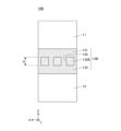
- FIG. 1 is a schematic diagram of an electromagnetic wave reflecting device to which a manufacturing method according to an embodiment is applied; 1 is a schematic diagram of an electromagnetic wave reflecting fence formed by connecting multiple electromagnetic wave reflecting devices.
- FIG. 2 is a diagram showing an example of a layer structure of an electromagnetic wave reflecting panel.
- 11A and 11B are diagrams showing another example of the layer structure of the electromagnetic wave reflecting panel. This is an image of air bubbles occurring inside an electromagnetic wave reflecting panel.
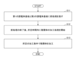
- 4 is a flowchart of a method for manufacturing an electromagnetic wave reflecting panel according to an embodiment.
- electromagnetic wave reflective panels are made up of a laminate of multiple materials, tiny air bubbles may form inside the electromagnetic wave reflective panel. Some of these bubbles are about 0.5 mm to 5.0 mm in size and can be seen with the naked eye. Visible air bubbles not only affect the reflective properties, but also the appearance of the electromagnetic wave reflective panel.
- the occurrence of air bubbles is suppressed by optimizing the conditions for pre-treatment of materials and the processing conditions for lamination during the manufacturing process of the electromagnetic wave reflective panel.
- the number of air bubbles of 5.0 mm or less observed by the naked eye is set to 20 or less, preferably 15 or less, more preferably 10 or less, and even more preferably 5 or less.
- the size of the air bubbles is the diameter for circular bubbles, the length of the major axis for elliptical bubbles, and the length for linear bubbles.
- the electromagnetic wave reflecting device 60 has an electromagnetic wave reflecting panel 10 and a frame 50 that holds the electromagnetic wave reflecting panel 10.
- the width or horizontal direction of the electromagnetic wave reflecting panel 10 when the electromagnetic wave reflecting device 60 is installed is the X direction
- the height or vertical direction is the Y direction
- the thickness direction is the Z direction.
- the electromagnetic wave reflecting panel 10 reflects radio waves of a desired band selected from a frequency band of 1 GHz to 300 GHz, for example, a frequency band of 1 GHz or more and 170 GHz or less.
- At least a part of the reflecting surface of the electromagnetic wave reflecting panel 10 may include a metasurface with a controlled reflection angle and reflection efficiency.
- Metasurfaces are formed with periodic patterns, mesh patterns, geometric patterns, etc., designed according to the desired reflection mode and frequency band, and their reflection properties such as reflection angle and reflection efficiency are controlled.
- the patterns that make up metasurfaces are formed from good conductors such as metals, or conductive films that are transparent to visible light. Control of the reflection angle includes the formation of non-specular reflection that reflects in a direction different from the angle of incidence, and control of the diffusion direction.
- the electromagnetic wave reflecting panel 10 may include at least a portion of a specular reflecting surface.
- the specular reflecting surface reflects incident electromagnetic waves in the same direction as the angle of incidence.
- the electromagnetic wave reflecting panel 10 may have a mixture of specular reflecting surfaces and non-specular reflecting surfaces.
- the frame 50 holds two sides along the height direction of the electromagnetic wave reflecting panel 10 when it is installed.
- a top frame 57 that holds the upper end of the electromagnetic wave reflecting panel 10
- a bottom frame 58 that holds the lower end may be provided.
- the frame 50, the top frame 57, and the bottom frame 58 form a frame that holds the entire perimeter of the electromagnetic wave reflecting panel 10.
- the frame 50 may be called a "side frame” based on its positional relationship to the top frame 57 and bottom frame 58.
- the electromagnetic wave reflecting device 60 may have legs 56 that support the frame 50. As shown in FIG. 1, it is desirable to provide the legs 56 when the electromagnetic wave reflecting device 60 is to be freestanding on an installation surface, but the legs 56 are not essential. Casters may be provided on the legs 56 to make it mobile, or the electromagnetic wave reflecting panel 10 may be installed on a wall surface or hung from the ceiling without providing the legs 56.
- the frame 50, the top frame 57, and the bottom frame 58 are formed with slits to receive the ends (edges) of the electromagnetic wave reflective panel 10.
- the ends of the electromagnetic wave reflective panel 10 are inserted into the slits formed in the frame 50, etc.
- the ends of the electromagnetic wave reflective panel 10 housed in the slits of the frame 50, etc. are not used to reflect the incident electromagnetic waves.
- the effective area is an area that is a predetermined dimension inward from the end of the electromagnetic wave reflective panel 10.
- the effective area is determined by the size of the frame 50, etc., and is, for example, an area that is more than 50.0 mm inward from the end of the electromagnetic wave reflective panel 10.
- the electromagnetic wave reflecting panel 10 suppresses the generation of microscopic bubbles in the effective area.
- the number of bubbles of 5.0 mm or less that can be observed with the naked eye is 20 or less, preferably 15 or less, more preferably 10 or less, and even more preferably 5 or less.
- FIG. 2 is a schematic diagram of an electromagnetic wave reflecting fence 100 in which electromagnetic wave reflecting devices 60-1, 60-2, and 60-3 are connected.
- three electromagnetic wave reflecting devices 60-1, 60-2, and 60-3 (hereinafter, collectively referred to as “electromagnetic wave reflecting devices 60" as appropriate) are connected to form the electromagnetic wave reflecting fence 100, but there is no particular limit to the number of electromagnetic wave reflecting devices 60 that are connected.
- Electromagnetic wave reflecting devices 60-1, 60-2, and 60-3 each have electromagnetic wave reflecting panels 10-1, 10-2, and 10-3, respectively. Adjacent electromagnetic wave reflecting panels are held together by a frame 50 to obtain an electromagnetic wave reflecting fence 100 connected in the X direction.
- Each of the electromagnetic wave reflecting panels 10-1, 10-2, and 10-3 (hereinafter sometimes collectively referred to as "electromagnetic wave reflecting panel 10") is manufactured by the method described below, and the number of air bubbles of 5.0 mm or less observed by the naked eye within the effective area is suppressed.
- ⁇ Layer structure of electromagnetic wave reflection panel> 3 shows an example of a layer structure of the electromagnetic wave reflection panel 10A.
- This layer structure is a structure in the thickness (Z) direction of the electromagnetic wave reflection panel 10A, and corresponds to the A-A cross section of FIG. 1.
- the electromagnetic wave reflection panel 10A has a first dielectric substrate 11, a second dielectric substrate 12, and an intermediate layer 13A provided between the first dielectric substrate 11 and the second dielectric substrate 12.
- the intermediate layer 13A is formed by laminating a first intermediate film 131, a second intermediate film 132A, and a third intermediate film 133 in this order.
- the interface between the first intermediate film 131 and the second intermediate film 132A, or the interface between the second intermediate film 132A and the third intermediate film 133 becomes a reflection surface that reflects electromagnetic waves of 1 GHz or more and 300 GHz or less, for example, 1 GHz or more and 170 GHz or less.
- the first dielectric substrate 11 and the second dielectric substrate 12 support the intermediate layer 13A from both sides.
- the first dielectric substrate 11 and the second dielectric substrate 12 are dielectric resin substrates or polymer sheets such as polycarbonate, cycloolefin polymer (COP), polyethylene terephthalate (PET), and fluororesin.
- polycarbonate which has excellent impact resistance, durability, and transparency.
- the thicknesses of the first dielectric substrate 11 and the second dielectric substrate 12 are appropriately selected in the range of 1.0 mm to 10.0 mm.
- the second intermediate film 132A is formed of a conductive material and reflects the incident electromagnetic waves.
- the material of the second intermediate film 132A may be stainless steel, mild steel, copper, copper oxide, nickel, nickel oxide, gold, silver, aluminum, or a combination of these.
- the thickness d of the second intermediate film 132A is smaller than the wavelength of the incident electromagnetic waves.
- the first intermediate film 131 and the third intermediate film 133 are dielectric resin films.
- resins that can be used include ethylene vinyl acetate, COP, UV-curable resin, thermosetting resin, and thermoplastic resin.
- UV-curable resins that can be used include urethane-based resin, acrylic-based resin, silicone-based resin, epoxy resin, and urethane acrylate.
- the first intermediate film 131 and the third intermediate film 133 may be made of the same or different materials, but it is desirable to form them from the same material so that the electromagnetic wave reflection panel 10A can be used with the same reflection characteristics from either direction without distinguishing between the front and back sides.
- the relative dielectric constant and dielectric loss tangent of the resin material of the first intermediate film 131 and the third intermediate film 133 are set within an appropriate range to suppress the decrease in reflection efficiency.
- the relative dielectric constant of the above resin material is 2.0 or more and less than 3.0, and the dielectric loss tangent is 0.0001 or more and less than 0.1000. If the relative dielectric constant of the first intermediate film 131 and the third intermediate film 133 is 3.0 or more, there is a risk of increased loss at high frequencies. Similarly, if the dielectric loss tangent of the first intermediate film 131 and the third intermediate film 133 is 0.1000 or more, there is a risk of increased loss of electrical energy in the resin film.
- tiny air bubbles may occur at the interface between the first dielectric substrate 11 and the first intermediate film 131, the interface between the first intermediate film 131 and the second intermediate film 132A, the interface between the second intermediate film 132A and the third intermediate film 133, and the interface between the third intermediate film 133 and the second dielectric substrate 12. If the number of air bubbles visible to the naked eye increases, the reflection characteristics are affected and the amount of reflection decreases. In the electromagnetic wave reflecting panel 10A, the number of air bubbles of 5.0 mm or less that are visible to the naked eye within a range of 50.0 mm x 50.0 mm within the effective area is 20 or less, preferably 15 or less, more preferably 10 or less, and even more preferably 5 or less.
- FIG. 4 shows an example of the layer structure of electromagnetic wave reflecting panel 10B.
- Electromagnetic wave reflecting panel 10B has a layer structure similar to that of electromagnetic wave reflecting panel 10A, except that second intermediate film 132B of intermediate layer 13B has an opening 135.
- Intermediate layer 13B is held between first dielectric substrate 11 and second dielectric substrate 12.
- Intermediate layer 13B is formed by stacking first intermediate film 131, second intermediate film 132B, and third intermediate film 133 in this order.
- the interface between first intermediate film 131 and second intermediate film 132B, or the interface between second intermediate film 132B and third intermediate film 133 becomes a reflective surface that reflects electromagnetic waves of 1 GHz or more and 300 GHz or less, for example, 1 GHz or more and 170 GHz or less.
- the materials, thicknesses, etc. of the first dielectric substrate 11, the second dielectric substrate 12, the first intermediate film 131, and the third intermediate film 133 are the same as those of the electromagnetic wave reflecting panel 10A.
- the opening 135 of the second intermediate film 132B may be a through hole having a rectangular, circular, elliptical, polygonal shape, or may be a mesh opening.
- the openings 135 penetrating the second intermediate film 132B may be formed in a periodic arrangement to enhance the selectivity of reflection for a specific frequency.
- the second intermediate film 132B may be formed in a mesh structure, and the mesh opening may be the opening 135 of the second intermediate film 132B.
- the thickness d of the second intermediate film 132B and the size (diameter) of the opening 135 are smaller than the wavelength of the incident electromagnetic wave.
- the opening ratio of the second intermediate film 132B is preferably 50% or more and 80% or less. If the opening ratio exceeds 80%, the desired reflection efficiency may not be obtained. If the opening ratio is less than 50%, the visible light transmittance of the electromagnetic wave reflection panel 10B may decrease. If transparency to visible light is not required depending on the manner in which the electromagnetic wave reflecting panel 10B is used, the aperture ratio of the opening 135 may be set to less than 50% to prioritize improving the reflection efficiency.
- the first intermediate film 131 and the third intermediate film 133 may be connected within the opening 135 of the second intermediate film 132B.
- the opening 135 does not need to be completely filled with the resin film, and may be 90.0% or more of the total area or volume of the opening 135 depending on the bonding conditions when forming the intermediate layer 13B.
- the first intermediate film 131 and the third intermediate film 133 may enter the opening 135 from both sides of the second intermediate film 132B, or either the first intermediate film 131 or the third intermediate film 133 may enter the opening 135.
- tiny air bubbles may occur at the interface between the first dielectric substrate 11 and the intermediate layer 13B, inside the intermediate layer 13B, and at the interface between the intermediate layer 13B and the second dielectric substrate 12. If the number of air bubbles visible to the naked eye increases, the reflection characteristics will be affected and the amount of reflection will decrease.
- the number of air bubbles of 5.0 mm or less that are visible to the naked eye is 20 or less, preferably 15 or less, more preferably 10 or less, and even more preferably 5 or less.
- samples are prepared under different conditions, and the return loss at a specified frequency is measured to identify the allowable range of bubbles.
- the return loss is measured using a spectrum network analyzer and a high-frequency oblique incidence free-space type S-parameter measurement jig. Electromagnetic waves of 28.0 GHz are perpendicularly incident and the perpendicular reflection is measured.
- the return loss is measured under the same perpendicular incidence condition using a smooth aluminum plate of 3.0 mm thickness and 300.0 mm x 300.0 mm, and this measurement value is set to a return loss of 0.00 dB at a frequency of 28.0 GHz.
- the return loss (absolute value) from the reference value is desirable for the return loss (absolute value) from the reference value to be less than 0.35 dB. Air bubbles that occur within the panel affect the reflection characteristics as well as the appearance of the electromagnetic wave reflecting panel, so it is desirable for their number to be small. In the example below, the number of tiny air bubbles of 5.0 mm or less that can be visually observed within a certain area and the return loss are measured.
- Example 1 is Example 1.
- a polycarbonate sheet having a length of 1.0 m, a width of 2.0 m, and a thickness of 2.0 mm is used as the first dielectric substrate 11 and the second dielectric substrate 12.
- a sample of the electromagnetic wave reflection panel 10 is produced by sandwiching the intermediate layer 13B between two polycarbonate sheets.
- the intermediate layer is a first intermediate film 131 of ethylene vinyl acetate having a thickness of 400 ⁇ m, a second intermediate film 132B of stainless steel mesh having a thickness of 100 ⁇ m, and a third intermediate film 133 of ethylene vinyl acetate having a thickness of 400 ⁇ m laminated in this order.
- the average opening diameter of the stainless steel mesh is 268 ⁇ m, and the average opening ratio is 71%.
- the thickness and opening diameter of the stainless steel mesh are smaller than the wavelength of the electromagnetic wave in the 28 GHz band.
- the two polycarbonate sheets used for the first dielectric substrate 11 and second dielectric substrate 12 are pre-treated by annealing at 80°C for 20 hours. After this pre-treatment is completed, the polycarbonate sheets are taken out to a room temperature environment and processing of the laminate begins within one hour.
- a laminate is formed by sandwiching an intermediate layer having the above-mentioned stainless steel mesh between the two pre-treated polycarbonate sheets. This laminate is placed in a vacuum or reduced pressure heat treatment furnace of 200 Pa or less. In the heat treatment furnace, it is heated and held at 0.5 atmospheres (50662.5 Pa) and 90°C for 30 minutes.
- Example 2 is Example 2.
- the laminated structure of the sample itself is the same as that of Example 1. That is, an intermediate layer 13B is arranged between two polycarbonate sheets each having a length of 1.0 m, a width of 2.0 m, and a thickness of 2.0 mm, to prepare a sample of an electromagnetic wave reflection panel 10.
- the design conditions of the intermediate layer 13B are also the same as those of Example 1, and an intermediate layer 13B is formed by arranging ethylene vinyl acetate having a thickness of 400 ⁇ m on both sides of a stainless steel mesh having a thickness of 100 ⁇ m.
- a pretreatment is performed under the same conditions as in Example 1.
- the two polycarbonate sheets are subjected to a heat treatment at 80° C. for 20 hours, and after this pretreatment, the polycarbonate sheets are taken out into a room temperature environment, and within one hour, processing to prepare a laminate is started.
- a laminate is formed by sandwiching an intermediate layer having the above-mentioned stainless steel mesh between two pretreated polycarbonate sheets, and the laminate is placed in a heat treatment furnace at 200 Pa or less. In the heat treatment furnace, the laminate is heated and held at 0.1 atmosphere (10132.5 Pa) and 90°C for 30 minutes. After pretreatment in which the polycarbonate sheet is held in a thermostatic chamber at 80°C for 20 hours, the above processing is carried out within 1 hour in a room temperature environment, and the appearance of the sample produced is visually inspected. The maximum number of bubbles of 5.0 mm or less observed with the naked eye in a 50.0 mm x 50.0 mm range within the effective area 5.0 mm inside from the edge of the sample was 10.
- the average reflection attenuation against the reference value at a frequency of 28.0 GHz was -0.19 dB, and the desired reflection characteristics were obtained.
- Example 3 is Example 3.
- the laminated structure of the sample itself is the same as that of Examples 1 and 2.
- two polycarbonate sheets used as the first dielectric substrate 11 and the second dielectric substrate 12 are subjected to a heat treatment at 80° C. for 20 hours.
- the processing of the laminate is started before 1.5 hours have passed since the polycarbonate sheets were taken out into a room temperature environment.
- a laminate is formed by disposing an intermediate layer having a stainless steel mesh between the two pretreated polycarbonate sheets, and the laminate is placed in a heat treatment furnace at 200 Pa or less.
- the average return loss against the reference value at a frequency of 28.0 GHz was -0.23 dB, and the desired reflection characteristics were obtained.
- Example 1 Compared to Example 1, the time spent in a room temperature environment after pretreatment before starting the lamination process was slightly longer, resulting in the formation of a few air bubbles, but both the appearance and reflective properties were good.
- Example 4 is Example 4.
- the laminated structure of the sample itself is the same as that of Examples 1 to 3.
- two polycarbonate sheets used as the first dielectric substrate 11 and the second dielectric substrate 12 are subjected to a heat treatment at 80° C. for 20 hours.
- the processing of the laminate is started within one hour after the polycarbonate sheets are taken out to a room temperature environment.
- a laminate is formed by disposing an intermediate layer having a stainless steel mesh between the two pretreated polycarbonate sheets, and this laminate is placed in a heat treatment furnace at 200 Pa or less.
- the laminate In the heat treatment furnace, the laminate is heated and held at 0.5 atmospheres (50662.5 Pa) and 75° C. for 30 minutes. After pretreatment in which the polycarbonate sheet was kept in a thermostatic chamber at 80°C for 20 hours, the above processing was carried out within 1 hour in a room temperature environment, and the appearance of the sample produced was visually inspected, and the maximum number of bubbles of 5.0 mm or less observed with the naked eye in a 50.0 mm x 50.0 mm range within the effective area 5.0 mm inside from the end of the sample was 2.
- the average return loss against the reference value at a frequency of 28.0 GHz was -0.30 dB, and the desired reflection characteristics were obtained.
- Example 1 Although the number of bubbles is sufficiently small, as in Example 1, the reflection attenuation is greater than in Example 1. This is thought to be because the heat treatment temperature in the processing of the laminate was set at a slightly lower temperature of 75°C, which increased the volume of bubbles remaining in the laminate. There are no problems with the appearance of this sample, and the reflection characteristics are within the acceptable range.
- Example 5 is Example 5.
- the laminated structure of the sample itself is the same as that of Examples 1 to 4.
- two polycarbonate sheets used as the first dielectric substrate 11 and the second dielectric substrate 12 are subjected to a heat treatment at 80° C. for 20 hours as a pretreatment.
- the polycarbonate sheets are taken out into a room temperature environment, and within one hour, the processing of the laminate is started.
- a laminate is formed by disposing an intermediate layer having a stainless steel mesh between the two pretreated polycarbonate sheets, and the laminate is placed in a heat treatment furnace at 200 Pa or less.
- the laminate In the heat treatment furnace, the laminate is heated and held at 0.5 atmospheres (50662.5 Pa) and 80° C. for 30 minutes. After pretreatment in which the polycarbonate sheet was kept in a thermostatic chamber at 80°C for 20 hours, the above processing was carried out within 1 hour in a room temperature environment, and the appearance of the sample produced was visually inspected with the naked eye. The number of bubbles of 5.0 mm or less observed with the naked eye in a 50.0 mm x 50.0 mm range within the effective area 5.0 mm inside from the edge of the sample was 0.
- the average return loss relative to the reference value at a frequency of 28.0 GHz was -0.32 dB, and the desired reflection characteristics were obtained.
- Example 6 is Example 6.
- the laminated structure of the sample itself is the same as that of Examples 1 to 5.
- two polycarbonate sheets used as the first dielectric substrate 11 and the second dielectric substrate 12 are subjected to a heat treatment at 80° C. for 20 hours as a pretreatment.
- the polycarbonate sheets are taken out into a room temperature environment and within one hour, the processing of the laminate is started.
- An intermediate layer having a stainless steel mesh is placed between the two pretreated polycarbonate sheets to form a laminate, and the laminate is placed in a heat treatment furnace at 200 Pa or less.
- the laminate In the heat treatment furnace, the laminate is heated and held at 0.5 atmospheres (50662.5 Pa) and 130° C. for 30 minutes. After pretreatment in which the polycarbonate sheet was kept in a thermostatic chamber at 80°C for 20 hours, the above processing was carried out within 1 hour in a room temperature environment, and the appearance of the sample produced was visually inspected. The number of bubbles of 5.0 mm or less observed by the naked eye was 0 in the range of 50.0 mm x 50.0 mm in the effective area inside 5.0 mm from the end of the sample.
- the average return loss against the reference value at a frequency of 28.0 GHz was -0.25 dB, and the desired reflection characteristics were obtained. It can be seen that both the appearance and the reflection characteristics are very good when the heating temperature is set to 130°C in the processing of the laminate.
- Example 7 is Example 7.
- the laminated structure of the sample itself is the same as that of Examples 1 to 6.
- two polycarbonate sheets used as the first dielectric substrate 11 and the second dielectric substrate 12 are subjected to a heat treatment at 80° C. for 20 hours as a pretreatment.
- the processing of the laminate is started within one hour after the polycarbonate sheets are taken out to a room temperature environment.
- a laminate is formed by disposing an intermediate layer having a stainless steel mesh between the two pretreated polycarbonate sheets, and the laminate is placed in a heat treatment furnace at 200 Pa or less.
- the laminate In the heat treatment furnace, the laminate is heated and held at 0.5 atmospheres (50662.5 Pa) and 110° C. for 30 minutes. After pretreatment in which the polycarbonate sheet was held in a thermostatic chamber at 80°C for 20 hours, the above processing was carried out within 1 hour in a room temperature environment, and the appearance of the sample was visually inspected. The number of bubbles of 5.0 mm or less observed by the naked eye was 0 in the 50.0 mm x 50.0 mm range in the effective area inside 5.0 mm from the end of the sample.
- the average return loss against the reference value at a frequency of 28.0 GHz was -0.22 dB, and the desired reflection characteristics were obtained. It can be seen that both the appearance and the reflection characteristics are good when the heating temperature of the processing of the laminate is 110°C.
- Example 8 is Example 8.
- the temperature and time of pretreatment are changed.
- two polycarbonate sheets used as the first dielectric substrate 11 and the second dielectric substrate 12 are subjected to a heat treatment at 40° C. for 40 hours.
- the processing of the laminate is started within one hour after the polycarbonate sheets are taken out into a room temperature environment.
- a laminate is formed by disposing an intermediate layer having a stainless steel mesh between the two pretreated polycarbonate sheets, and the laminate is placed in a heat treatment furnace at 200 Pa or less.
- the laminate In the heat treatment furnace, the laminate is heated and held at 0.5 atmospheres (50662.5 Pa) and 110° C. for 30 minutes. After pretreatment in which a polycarbonate sheet is held in a thermostatic chamber at 40° C. for 40 hours, the above processing is carried out within 1 hour in a room temperature environment, and the appearance of the sample produced is visually inspected.
- the number of bubbles of 5.0 mm or less observed by the naked eye in a range of 50.0 mm ⁇ 50.0 mm in the effective area inside 5.0 mm from the end of the sample was 0.
- the average return loss relative to the reference value at a frequency of 28.0 GHz was ⁇ 0.22 dB, and the desired reflection characteristics were obtained. It can be seen that both the appearance and the reflection characteristics are good when the laminate is held at a pretreatment temperature of 40° C. for 8 hours or more, removed from the thermostatic chamber, and processed at a heating temperature of 110° C. within 1 hour.
- Example 9 is the embodiment 9.
- the temperature and time of the pretreatment are also changed.
- two polycarbonate sheets used as the first dielectric substrate 11 and the second dielectric substrate 12 are subjected to a heat treatment at 110° C. for 4 hours.
- the processing of the laminate is started within 1 hour after the polycarbonate sheets are taken out to a room temperature environment.
- a laminate is formed by disposing an intermediate layer having a stainless steel mesh between the two pretreated polycarbonate sheets, and the laminate is placed in a heat treatment furnace at 200 Pa or less.
- the laminate In the heat treatment furnace, the laminate is heated and held at 0.5 atmospheres (50662.5 Pa) and 110° C. for 30 minutes. After pretreatment in which a polycarbonate sheet was held in a thermostatic chamber at 110°C for 4 hours, the above processing was carried out within 1 hour in a room temperature environment, and the appearance of the sample was visually inspected. The number of bubbles of 5.0 mm or less observed by the naked eye was 0 in the range of 50.0 mm x 50.0 mm in the effective area inside 5.0 mm from the end of the sample.
- the average return loss relative to the reference value at a frequency of 28.0 GHz was -0.22 dB, and the desired reflection characteristics were obtained. It can be seen that both the appearance and the reflection characteristics are good when the laminate is held at a pretreatment temperature of 110°C for 4 hours, taken out of the thermostatic chamber, and processed at a heating temperature of 110°C within 1 hour.
- Example 10 is Comparative Example 1.
- the laminated structure of the sample itself is the same as that of Examples 1 to 9.
- the same pretreatment as that of Examples 1 to 7 is performed prior to processing of a laminate having a first dielectric substrate 11, an intermediate layer 13B, and a second dielectric substrate 12 in this order.
- Two polycarbonate sheets used as the first dielectric substrate 11 and the second dielectric substrate 12 are subjected to a heat treatment at 80° C. for 20 hours. After the pretreatment is completed, the polycarbonate sheets are taken out into a room temperature environment, and then processing of the laminate is started 5 hours later.
- An intermediate layer having a stainless steel mesh is placed between the two pretreated polycarbonate sheets to form a laminate, and the laminate thus produced is placed in a heat treatment furnace at 200 Pa or less.
- the laminate is heated and held at 0.5 atmospheres (50662.5 Pa) and 90° C. for 30 minutes.
- a polycarbonate sheet was pretreated by holding it in a thermostatic chamber at 80° C. for 20 hours, and then left in a room temperature environment for 5 hours before visually inspecting the appearance of the sample produced by the above processing.
- the maximum number of bubbles of 5.0 mm or less observed by the naked eye in a 50.0 mm ⁇ 50.0 mm area within the effective area 5.0 mm inside from the end of the sample was 50.
- the desired reflection characteristics were not obtained, including a location where the return attenuation relative to the reference value was ⁇ 0.75 dB at a frequency of 28.0 GHz.
- Example 1 Compared to Example 1, the laminate was left in a room temperature environment for a long time (5 hours) before processing, which is thought to be because air was trapped at the interfaces of each layer, and even after the laminate was subsequently subjected to a heat treatment, many air bubbles remained inside the laminate.
- Example 11 is Comparative Example 2.
- the laminated structure of the sample itself is the same as that of Examples 1 to 9.
- the same pretreatment as that of Examples 1 to 7 is performed prior to processing of a laminate having a first dielectric substrate 11, an intermediate layer 13B, and a second dielectric substrate 12 in this order.
- Two polycarbonate sheets used as the first dielectric substrate 11 and the second dielectric substrate 12 are subjected to a heat treatment at 80° C. for 20 hours. After the pretreatment is completed, the polycarbonate sheets are taken out into a room temperature environment, and 10 hours later, the processing of the laminate is started.
- a laminate is formed by disposing an intermediate layer having a stainless steel mesh between the two pretreated polycarbonate sheets, and the laminate is placed in a heat treatment furnace at 200 Pa or less. As in Example 1, the laminate is heated and held at 0.5 atmospheres (50662.5 Pa) and 90° C. for 30 minutes.
- a polycarbonate sheet was kept in a thermostatic chamber at 80° C. for 20 hours, and then left in a room temperature environment for 10 hours before visually inspecting the appearance of a sample produced by the above processing.
- the maximum number of bubbles of 5.0 mm or less observed by the naked eye in a 50.0 mm ⁇ 50.0 mm area within an effective area 5.0 mm inside from the end of the sample was 70.
- the reflection attenuation at a frequency of 28.0 GHz was -0.90 dB relative to the reference value, including a portion where the reflection characteristic was not as desired.
- Example 12 is Comparative Example 3.
- the laminated structure of the sample itself is the same as that of Examples 1 to 9.
- the same pretreatment as that of Examples 1 to 7 is performed prior to processing of a laminate having a first dielectric substrate 11, an intermediate layer 13B, and a second dielectric substrate 12 in this order.
- Two polycarbonate sheets used as the first dielectric substrate 11 and the second dielectric substrate 12 are subjected to a heat treatment at 80° C. for 20 hours. After the pretreatment is completed, the processing of the laminate is started within one hour after the polycarbonate sheets are taken out to a room temperature environment.
- a laminate is formed by disposing an intermediate layer having a stainless steel mesh between the two pretreated polycarbonate sheets, and the laminate is placed in a heat treatment furnace at 200 Pa or less.
- Example 1 the laminate is heated and held at 0.01 atmosphere (1013.3 Pa) and 90° C. for 30 minutes in a heat treatment furnace.
- a polycarbonate sheet was pretreated in a thermostatic chamber at 80° C. for 20 hours, and then processed in a room temperature environment within 1 hour.
- a visual inspection of the appearance of the sample produced showed that the maximum number of bubbles of 5.0 mm or less observed with the naked eye in a 50.0 mm ⁇ 50.0 mm area within the effective area 5.0 mm inside from the end of the sample was 100.
- the reflection attenuation at a frequency of 28.0 GHz relative to the reference value included a portion where it was ⁇ 1.02 dB, and the desired reflection characteristics were not obtained.
- the laminate After the pretreatment, the laminate is left in a room temperature environment for the same amount of time before processing begins as in Example 1, and processing of the laminate begins immediately after pretreatment. However, because the pressure during processing of the laminate is very low at 0.01 atmospheres, it is believed that air could not be sufficiently expelled from the laminate.
- Figure 5 is an image of the sample produced in Example 10. Air bubbles 101 with a length of about 3.0 mm have occurred in the electromagnetic wave reflection panel. In this image, only two air bubbles 101 are captured, but the air bubbles 101 have occurred randomly in an area of 50.0 mm x 50.0 mm. The air bubbles 101 cause a large return attenuation, and the designed reflection characteristics cannot be obtained. Air bubbles 101 observed with the naked eye are often recognized as scratches, and are undesirable in appearance.
- the following can be derived.
- the polycarbonate sheets used as the first and second dielectric substrates are not left in a room temperature environment for more than 5 hours after the pretreatment is performed until the processing of the laminate sandwiching the stainless steel mesh is started. It is preferable to start the processing of the laminate before 5 hours have passed after the end of the pretreatment.
- the pretreatment when the laminate is processed in a vacuum or reduced pressure heat treatment furnace, it is desirable to heat it at a temperature of 75° C. or higher and 130° C. or lower.
- FIG. 6 is a flow chart of a method for manufacturing an electromagnetic wave reflecting panel 10 according to an embodiment.
- a pretreatment is applied to the first dielectric substrate 11 and the second dielectric substrate 12 (S11).
- S11 the first dielectric substrate 11 and the second dielectric substrate 12
- an annealing treatment is performed at a constant temperature for a constant time.
- the optimal heating temperature and heating time differ depending on the resin material used, but when a polycarbonate sheet is used, it is heated at 40°C or higher and 120°C or lower for 8 hours or more.
- This pretreatment removes residual stress in the thermoplastic resin sheet.
- This pretreatment may include lowering the temperature to near room temperature in a thermostatic chamber.
- the processing of the laminate is started within a predetermined time after the first dielectric substrate and the second dielectric substrate are taken out of the thermostatic chamber and placed in a room temperature environment (S12). Specifically, it is desirable to start the processing of the laminate before 5 hours have elapsed after the first dielectric substrate and the second dielectric substrate are taken out of the thermostatic chamber and placed in a room temperature environment, and more preferably within a few hours.
- the laminate is processed under predetermined processing conditions (S13).
- the processing temperature of the laminate is preferably 75°C or higher and 130°C or lower. If the temperature is lower than 75°C, it becomes difficult to fully remove air bubbles inside the electromagnetic wave reflecting panel 10. If the temperature exceeds 130°C, the first dielectric substrate and the second dielectric substrate may be deformed.
- the processing pressure of the laminate is set to be higher than 0.01 atmospheres (1013.3 Pa), and preferably to be higher than 0.1 atmospheres (10132.5 Pa) and lower than 0.5 atmospheres (50662.5 Pa).
- the return loss of the electromagnetic wave reflecting device 60 and the electromagnetic wave reflecting fence 100 can be suppressed, and the reflection characteristics designed at the installation site can be exhibited.
- the in-plane size of the electromagnetic wave reflecting panel 10 can be appropriately selected within a range of 30 cm x 30 cm to 3 m x 3 m.
- the entire surface of the electromagnetic wave reflecting panel 10 may be a metasurface, or a portion may be a mirror-reflective surface. Within the effective reflection area of the electromagnetic wave reflecting panel 10, tiny air bubbles visible to the naked eye are suppressed, and the reflection characteristics and appearance can be maintained at a good level.
- An electromagnetic wave reflection panel that reflects electromagnetic waves in a predetermined frequency band ranging from 1 GHz to 300 GHz, A first dielectric substrate; A second dielectric substrate; an intermediate layer provided between the first dielectric substrate and the second dielectric substrate; having The number of bubbles of 5.0 mm or less observed by the naked eye within an area of 50.0 mm x 50.0 mm of the electromagnetic wave reflective panel is 20 or less.
- Electromagnetic wave reflecting panel the intermediate layer is formed by laminating a first intermediate film, a second intermediate film, and a third intermediate film in this order; The second intermediate film constitutes a reflecting surface that reflects the electromagnetic wave. Item 2.
- An electromagnetic wave reflecting panel according to item 1. (Item 3)
- the first intermediate film and the third intermediate film are dielectric resin films.
- Item 3. An electromagnetic wave reflecting panel according to item 2.
- the dielectric constant of the dielectric resin film is 2.0 or more and 3.0 or less, and the dielectric loss tangent is 0.0001 or more and less than 0.1000.
- Item 4. An electromagnetic wave reflecting panel according to item 3.
- the first dielectric substrate and the second dielectric substrate are resin substrates; Item 5.
- An electromagnetic wave reflecting panel according to any one of items 1 to 4. (Item 6) Item 6.
- An electromagnetic wave reflection panel according to any one of items 1 to 5; A frame for holding the electromagnetic wave reflecting panel; having In the effective reflection area of the electromagnetic wave reflection panel that is not covered by the frame, the number of bubbles of 5.0 mm or less observed by the naked eye within the 50.0 mm x 50.0 mm area is 20 or less.
- Electromagnetic wave reflector. (Item 7) Item 7. An electromagnetic wave reflecting fence comprising a plurality of electromagnetic wave reflecting devices according to item 6 connected by the frame.
- a first dielectric substrate and a second dielectric substrate, each of which is transparent to electromagnetic waves in a predetermined frequency band in the range of 1 GHz to 300 GHz, are pretreated; after the pretreatment is completed, the first dielectric substrate and the second dielectric substrate are taken out into a room temperature environment, and within a predetermined time, a processing process of a laminate using the first dielectric substrate and the second dielectric substrate is started; preparing a laminate in which an intermediate layer is disposed between the first dielectric substrate and the second dielectric substrate; The laminate is heated at a temperature of 75° C. or more and 130° C. or less to form an electromagnetic wave reflective panel.
- a method for manufacturing an electromagnetic wave reflecting panel are pretreated; after the pretreatment is completed, the first dielectric substrate and the second dielectric substrate are taken out into a room temperature environment, and within a predetermined time, a processing process of a laminate using the first dielectric substrate and the second dielectric substrate is started; preparing a laminate in which an intermediate layer is disposed between the first dielectric substrate and the
- the processing of the laminate is started within 5 hours after the first dielectric substrate and the second dielectric substrate are removed from the thermostatic chamber at 40° C. or higher and 120° C. or lower to a room temperature environment prior to the processing.
- Item 9. A method for producing an electromagnetic wave reflecting panel according to item 8. (Item 10) When heating the laminate, a pressure higher than 1013.3 Pa is set.
- Item 10. A method for producing an electromagnetic wave reflecting panel according to item 8 or 9.
- the pressure is set to 10132.5 Pa or more and 50662.5 Pa or less.
- Item 11 A method for producing an electromagnetic wave reflecting panel according to item 10.
- Electromagnetic wave reflecting panel 11 First dielectric substrate 12 Second dielectric substrate 13A, 13B Intermediate layer 50 Frame (side frame) 57 Top frame 58 Bottom frame 60, 60-1, 60-2, 60-3 Electromagnetic wave reflection device 100 Electromagnetic wave reflection fence 101 Air bubble 131 First intermediate film 132 Second intermediate film 133 Third intermediate film 135 Opening
Landscapes
- Physics & Mathematics (AREA)
- Electromagnetism (AREA)
- Laminated Bodies (AREA)
- Aerials With Secondary Devices (AREA)
Abstract
Description
前記電磁波反射パネルの50.0mm×50.0mmの範囲で、肉眼で観察される5.0mm以下の気泡の数は20個以下である。
図3は、電磁波反射パネル10Aの層構成の一例を示す。この層構成は、電磁波反射パネル10Aの厚さ(Z)方向の構成であり、図1のA-A断面に相当する。電磁波反射パネル10Aは、第1の誘電体基板11と、第2の誘電体基板12と、第1の誘電体基板11と第2の誘電体基板12の間に設けられる中間層13Aを有する。中間層13Aは、第1中間膜131、第2中間膜132A、及び第3中間膜133が、この順で積層されている。電磁波の入射方向によって、第1中間膜131と第2中間膜132Aの界面、または第2中間膜132Aと第3中間膜133の界面は、1GHz以上300GHz以下、たとえば1GHz以上170GHz以下の電磁波を反射する反射面となる。
例1は、実施例1である。第1の誘電体基板11及び第2の誘電体基板12として、縦1.0m、横2.0m、厚さ2.0mmのポリカーボネートシートを用いる。2枚のポリカーボネートシートで中間層13Bを挟んで、電磁波反射パネル10のサンプルを作製する。中間層は、厚さ400μmのエチレン酢酸ビニルの第1中間膜131と、厚さ100μmのステンレスメッシュの第2中間膜132Bと、厚さ400μmのエチレン酢酸ビニルの第3中間膜133がこの順で積層されている。ステンレスメッシュの平均開口径は268μm、平均開口率は71%である。ステンレスメッシュの厚さと開口径は、28GHz帯の電磁波の波長よりも小さい。
例2は、実施例2である。サンプルの積層構成自体は、例1と同じである。すなわち、それぞれが縦1.0m、横2.0m、厚さ2.0mmの2枚のポリカーボネートシートの間に中間層13Bを配置して、電磁波反射パネル10のサンプルを作製する。中間層13Bの設計条件も例1と同じであり、厚さ100μmのステンレスメッシュの両面に厚さ400μmのエチレン酢酸ビニルを配置した中間層13Bを形成する。第1の誘電体基板11、中間層13B、及び第2の誘電体基板12をこの順で有する積層体の加工処理に先立って、例1と同じ条件で前処理を施す。2枚のポリカーボネートシートに、80℃で20時間の加熱処理を施し、この前処理の後、ポリカーボネートシートを室温環境に取り出してから1時間以内で、積層体を作製する加工処理を開始する。
例3は、実施例3である。サンプルの積層構成自体は、例1及び例2と同じである。第1の誘電体基板11、中間層13B、及び第2の誘電体基板12をこの順で有する積層体の加工処理に先立って、第1の誘電体基板11及び第2の誘電体基板12として用いる2枚のポリカーボネートシートに、80℃で20時間の加熱処理を施す。この前処理の終了後、ポリカーボネートシートを室温環境に取り出してから1.5時間が経過する前に、積層体の加工処理を開始する。前処理がされた2枚のポリカーボネートシートの間に、ステンレスメッシュを有する中間層を配置して積層体を形成し、この積層体を、200Pa以下の熱処理炉に入れる。0.5気圧(50662.5Pa)、90℃で30分加熱保持する。ポリカーボネートシートを80℃の恒温槽で20時間保持する前処理の後、室温環境で1.5時間以内に前記加工を行って作製されたサンプルの外観検査を目視で行ったところ、サンプルの端部から5.0mmよりも内側の有効領域内の50.0mm×50.0mmの範囲で、肉眼で観察される気泡の最大数は、5個であった。高周波用斜め入射フリースペースタイプのSパラメータ測定法の垂直入射条件でパネルの反射面の6か所で垂直反射の減衰を測定したところ、周波数28.0GHzにおいて基準値に対する平均反射減衰は-0.23dBであり、所望の反射特性が得られた。
例4は、実施例4である。サンプルの積層構成自体は、例1から例3と同じである。第1の誘電体基板11、中間層13B、及び第2の誘電体基板12をこの順で有する積層体の加工処理に先立って、第1の誘電体基板11及び第2の誘電体基板12として用いる2枚のポリカーボネートシートに、80℃で20時間の加熱処理を施す。この前処理の終了後、ポリカーボネートシートを室温環境に取り出してから1時間以内に、積層体の加工処理を開始する。前処理がされた2枚のポリカーボネートシートの間に、ステンレスメッシュを有する中間層を配置して積層体を形成し、この積層体を、200Pa以下の熱処理炉に入れる。熱処理炉内で、0.5気圧(50662.5Pa)、75℃で30分加熱保持する。ポリカーボネートシートを80℃の恒温槽で20時間保持する前処理の後、室温環境で1時間以内に前記加工を行って作製されたサンプルの外観検査を目視で行ったところ、サンプルの端部から5.0mmよりも内側の有効領域内の50.0mm×50.0mmの範囲で、肉眼で観察される5.0mm以下の気泡の最大数は2個であった。高周波用斜め入射フリースペースタイプのSパラメータ測定法の垂直入射条件でパネルの反射面の6か所で垂直反射の減衰を測定したところ、周波数28.0GHzにおいて基準値に対する平均反射減衰は-0.30dBであり、所望の反射特性が得られた。
例5は、実施例5である。サンプルの積層構成自体は、例1から例4と同じである。第1の誘電体基板11、中間層13B、及び第2の誘電体基板12をこの順で有する積層体の加工処理に先立って、前処理として、第1の誘電体基板11及び第2の誘電体基板12として用いる2枚のポリカーボネートシートに、80℃で20時間の加熱処理を施す。前処理の終了後、ポリカーボネートシートを室温環境に取り出してから1時間以内のうちに、積層体の加工処理を開始する。前処理がされた2枚のポリカーボネートシートの間に、ステンレスメッシュを有する中間層を配置して積層体を形成し、作製した積層体を、200Pa以下の熱処理炉に入れる。熱処理炉内で、0.5気圧(50662.5Pa)、80℃で30分加熱保持する。ポリカーボネートシートを80℃の恒温槽で20時間保持する前処理の後、室温環境で1時間以内に前記加工を行って作製されたサンプルの外観検査を肉眼による目視で行ったところ、サンプルの端部から5.0mmよりも内側の有効領域内の50.0mm×50.0mmの範囲で、肉眼で観察される5.0mm以下の気泡の数は0個であった。高周波用斜め入射フリースペースタイプのSパラメータ測定法の垂直入射条件で、パネルの反射面の6か所で垂直反射の減衰を測定したところ、周波数28.0GHzにおいて基準値に対する平均反射減衰は-0.32dBであり、所望の反射特性が得られた。
例6は、実施例6である。サンプルの積層構成自体は、例1から例5と同じである。第1の誘電体基板11、中間層13B、及び第2の誘電体基板12をこの順で有する積層体の加工処理に先立って、前処理として、第1の誘電体基板11及び第2の誘電体基板12として用いる2枚のポリカーボネートシートに、80℃で20時間の加熱処理を施す。この前処理の終了後、ポリカーボネートシートを室温環境に取り出してから1時間以内に、積層体の加工処理を開始する。前処理がされた2枚のポリカーボネートシートの間に、ステンレスメッシュを有する中間層を配置して積層体を形成し、積層体を200Pa以下の熱処理炉に入れる。熱処理炉内で、0.5気圧(50662.5Pa)、130℃で30分加熱保持する。ポリカーボネートシートを80℃の恒温槽で20時間保持する前処理の後、室温環境で1時間以内に前記加工を行って作製されたサンプルの外観検査を目視で行ったところ、サンプルの端部から5.0mmよりも内側の有効領域内の50.0mm×50.0mmの範囲で、肉眼で観察される5.0mm以下の気泡の数は0個であった。高周波用斜め入射フリースペースタイプのSパラメータ測定法の垂直入射条件で、パネルの反射面の6か所で垂直反射の減衰を測定したところ、周波数28.0GHzにおいて基準値に対する平均反射減衰は-0.25dBであり、所望の反射特性が得られた。積層体の加工処理で、加熱温度を130℃に設定したときに、外観と反射特性の両方が非常に良好であることがわかる。
例7は、実施例7である。サンプルの積層構成自体は、例1から例6と同じである。第1の誘電体基板11、中間層13B、及び第2の誘電体基板12をこの順で有する積層体の加工処理に先立って、前処理として、第1の誘電体基板11及び第2の誘電体基板12として用いる2枚のポリカーボネートシートに、80℃で20時間の加熱処理を施す。前処理の後、ポリカーボネートシートを室温環境に取り出してから1時間以内に、積層体の加工処理を開始する。前処理がされた2枚のポリカーボネートシートの間に、ステンレスメッシュを有する中間層を配置して積層体を形成し、作製した積層体を、200Pa以下の熱処理炉に入れる。熱処理炉内で、0.5気圧(50662.5Pa)、110℃で30分加熱保持する。ポリカーボネートシートを80℃の恒温槽で20時間保持する前処理の後、室温環境で1時間以内に前記加工を行って作製されたサンプルの外観検査を目視で行ったところ、サンプルの端部から5.0mmよりも内側の有効領域内の50.0mm×50.0mmの範囲で、肉眼で観察される5.0mm以下の気泡の数は0個であった。高周波用斜め入射フリースペースタイプのSパラメータ測定法の垂直入射条件で、パネルの反射面の6か所で垂直反射の減衰を測定したところ、周波数28.0GHzにおいて基準値に対する平均反射減衰は-0.22dBであり、所望の反射特性が得られた。積層体の加工処理の加熱温度が110℃のときに、外観と反射特性の両方が良好であることがわかる。
例8は、実施例8である。例8では、前処理の温度と時間を変更する。第1の誘電体基板11、中間層13B、及び第2の誘電体基板12をこの順で有する積層体の加工処理に先立って、第1の誘電体基板11及び第2の誘電体基板12として用いる2枚のポリカーボネートシートに、40℃で40時間の加熱処理を施す。この前処理の後、ポリカーボネートシートを室温環境に取り出してから1時間以内に、積層体の加工処理を開始する。前処理がされた2枚のポリカーボネートシートの間に、ステンレスメッシュを有する中間層を配置して積層体を形成し、作製した積層体を、200Pa以下の熱処理炉に入れる。熱処理炉内で、0.5気圧(50662.5Pa)、110℃で30分加熱保持する。ポリカーボネートシートを40℃の恒温槽で40時間保持する前処理の後、室温環境で1時間以内に前記加工を行って作製されたサンプルの外観検査を目視で行ったところ、サンプルの端部から5.0mmよりも内側の有効領域内の50.0mm×50.0mmの範囲で、肉眼で観察される5.0mm以下の気泡の数は0個であった。高周波用斜め入射フリースペースタイプのSパラメータ測定法の垂直入射条件で、パネルの反射面の6か所で垂直反射の減衰を測定したところ、周波数28.0GHzにおいて基準値に対する平均反射減衰は-0.22dBであり、所望の反射特性が得られた。前処理の温度40℃で8時間以上保持し、恒温槽から取り出して1時間以内に110℃の加熱温度で積層体を加工したときに、外観と反射特性の両方が良好であることがわかる。
例9は、実施例9である。例9でも、前処理の温度と時間を変更する。第1の誘電体基板11、中間層13B、及び第2の誘電体基板12をこの順で有する積層体の加工処理に先立って、第1の誘電体基板11及び第2の誘電体基板12として用いる2枚のポリカーボネートシートに、110℃で4時間の加熱処理を施す。この前処理の後、ポリカーボネートシートを室温環境に取り出してから1時間以内に、積層体の加工処理を開始する。前処理がされた2枚のポリカーボネートシートの間に、ステンレスメッシュを有する中間層を配置して積層体を形成し、作製した積層体を、200Pa以下の熱処理炉に入れる。熱処理炉内で、0.5気圧(50662.5Pa)、110℃で30分加熱保持する。ポリカーボネートシートを110℃の恒温槽で4時間保持した前処理の後、室温環境で1時間以内に前記加工を行って作製されたサンプルの外観検査を目視で行ったところ、サンプルの端部から5.0mmよりも内側の有効領域内の50.0mm×50.0mmの範囲で、肉眼で観察される5.0mm以下の気泡の数は0個であった。高周波用斜め入射フリースペースタイプのSパラメータ測定法の垂直入射条件で、パネルの反射面の6か所で垂直反射の減衰を測定したところ、周波数28.0GHzにおいて基準値に対する平均反射減衰は-0.22dBであり、所望の反射特性が得られた。前処理の温度110℃で4時間保持し、恒温槽から取り出して1時間以内に110℃の加熱温度で積層体を加工したときに、外観と反射特性の両方が良好であることがわかる。
例10は、比較例1である。サンプルの積層構成自体は、例1から例9と同じである。第1の誘電体基板11、中間層13B、及び第2の誘電体基板12をこの順で有する積層体の加工処理に先立って、例1から例7と同じ前処理を行う。第1の誘電体基板11及び第2の誘電体基板12として用いる2枚のポリカーボネートシートに、80℃で20時間の加熱処理を施す。前処理の終了後に、ポリカーボネートシートを室温環境に取り出してから5時間経過してから、積層体の加工処理を開始する。前処理がされた2枚のポリカーボネートシートの間に、ステンレスメッシュを有する中間層を配置して積層体を形成し、作製した積層体を、200Pa以下の熱処理炉に入れる。例1と同じく、0.5気圧(50662.5Pa)、90℃で30分加熱保持する。ポリカーボネートシートを80℃の恒温槽で20時間保持する前処理の後、室温環境で5時間経過してから前記加工を行って作製されたサンプルの外観検査を目視で行ったところ、サンプルの端部から5.0mmよりも内側の有効領域内の50.0mm×50.0mmの範囲で、肉眼で観察される5.0mm以下の気泡の最大数は、50個であった。高周波用斜め入射フリースペースタイプのSパラメータ測定法の垂直入射条件で垂直反射の減衰を測定したところ、周波数28.0GHzにおいて基準値に対する反射減衰が-0.75dBとなる箇所を含み、所望の反射特性が得られなかった。
例11は、比較例2である。サンプルの積層構成自体は、例1から例9と同じである。第1の誘電体基板11、中間層13B、及び第2の誘電体基板12をこの順で有する積層体の加工処理に先立って、例1から例7と同じ前処理を行う。第1の誘電体基板11及び第2の誘電体基板12として用いる2枚のポリカーボネートシートに、80℃で20時間の加熱処理を施す。前処理の終了後に、ポリカーボネートシートを室温環境に取り出してから10時間経過してから、積層体の加工処理を開始する。前処理がされた2枚のポリカーボネートシートの間に、ステンレスメッシュを有する中間層を配置して積層体を形成し、作製した積層体を、200Pa以下の熱処理炉に入れる。例1と同じく、0.5気圧(50662.5Pa)、90℃で30分加熱保持する。ポリカーボネートシートを80℃の恒温槽で20時間保持した後、室温環境で10時間経過してから前記加工を行って作製されたサンプルの外観検査を肉眼による目視で行ったところ、サンプルの端部から5.0mmよりも内側の有効領域内の50.0mm×50.0mmの範囲で、肉眼で観察される5.0mm以下の気泡の最大数は70個であった。高周波用斜め入射フリースペースタイプのSパラメータ測定法の垂直入射条件で垂直反射の減衰を測定したところ、周波数28.0GHzにおいて基準値に対する反射減衰が-0.90dBとなる箇所を含み、所望の反射特性を得られなかった。
例12は、比較例3である。サンプルの積層構成自体は、例1から例9と同じである。第1の誘電体基板11、中間層13B、及び第2の誘電体基板12をこの順で有する積層体の加工処理に先立って、例1から例7と同じ前処理を行う。第1の誘電体基板11及び第2の誘電体基板12として用いる2枚のポリカーボネートシートに、80℃で20時間の加熱処理を施す。前処理の終了後、ポリカーボネートシートを室温環境に取り出してから1時間以内に、積層体の加工処理を開始する。前処理がされた2枚のポリカーボネートシートの間に、ステンレスメッシュを有する中間層を配置して積層体を形成し、作製した積層体を、200Pa以下の熱処理炉に入れる。例1と異なり、熱処理炉で、0.01気圧(1013.3Pa)、90℃で30分加熱保持する。ポリカーボネートシートを80℃の恒温槽で20時間保持する前処理の後、室温環境で1時間以内に前記加工を行って作製されたサンプルの外観検査を目視で行ったところ、サンプルの端部から5.0mmよりも内側の有効領域内の50.0mm×50.0mmの範囲で、肉眼で観察される5.0mm以下の気泡の最大数は100個であった。高周波用斜め入射フリースペースタイプのSパラメータ測定法の垂直入射条件で垂直反射の減衰を測定したところ、周波数28.0GHzにおいて基準値に対する反射減衰が-1.02dBとなる箇所を含み、所望の反射特性を得られなかった。
(1)第1及び第2の誘電体基板として用いるポリカーボネートシートに前処理を施してから、ステンレスメッシュを挟んだ積層体の加工処理の開始まで、5時間以上、室温環境に放置しないほうが望ましい。前処理が終了してから、5時間が経過する前に積層体の加工処理を開始するのが望ましい。
(2)前処理の後、積層体を真空または減圧の熱処理炉で加工する際に、75℃以上130以下の温度で加熱するのが望ましい。
(3)前処理の後、積層体を真空または減圧の熱処理炉で加工する際に、圧力を0.01気圧(1013.3Pa)より高く、たとえば0.1気圧(10132.5Pa)以上0.5気圧(50662.5Pa)以下に設定するのが望ましい。
(項1)
1GHz以上300GHz以下の範囲の所定の周波数帯の電磁波を反射する電磁波反射パネルにおいて、
第1の誘電体基板と、
第2の誘電体基板と、
前記第1の誘電体基板と前記第2の誘電体基板の間に設けられる中間層と、
を有し、
前記電磁波反射パネルの50.0mm×50.0mmの範囲で、肉眼で観察される5.0mm以下の気泡の数は20個以下である、
電磁波反射パネル。
(項2)
前記中間層は、第1中間膜、第2中間膜、及び第3中間膜がこの順で積層されており、
前記第2中間膜は前記電磁波を反射する反射面を構成する、
項1に記載の電磁波反射パネル。
(項3)
前記第1中間膜と前記第3中間膜は誘電体の樹脂膜である、
項2に記載の電磁波反射パネル。
(項4)
前記誘電体の樹脂膜の比誘電率は2.0以上3.0以下、誘電正接は0.0001以上0.1000未満である、
項3に記載の電磁波反射パネル。
(項5)
前記第1の誘電体基板と前記第1の誘電体基板は樹脂基板である、
項1から4のいずれかに記載の電磁波反射パネル。
(項6)
項1から5のいずれかに記載の電磁波反射パネルと、
前記電磁波反射パネルを保持するフレームと、
を有し、
前記電磁波反射パネルの前記フレームで覆われていない有効反射領域において、前記50.0mm×50.0mmの範囲で、肉眼で観察される5.0mm以下の気泡の数は20個以下である、
電磁波反射装置。
(項7)
項6に記載の電磁波反射装置を複数、前記フレームで連結した
電磁波反射フェンス。
(項8)
1GHz以上300GHz以下の範囲の所定の周波数帯の電磁波に対して透明な第1の誘電体基板と第2の誘電体基板に前処理を施し、
前記前処理の終了後に前記第1の誘電体基板と前記第2の誘電体基板を室温環境に取り出してから所定時間内に、前記第1の誘電体基板と前記第2の誘電体基板を用いた積層体の加工処理を開始し、
前記第1の誘電体基板と前記第2の誘電体基板の間に中間層を配置した積層体を作製し、
前記積層体を75℃以上130℃以下の温度で加熱して電磁波反射パネルを形成する、
電磁波反射パネルの製造方法。
(項9)
前記加工処理の以前に前記第1の誘電体基板と前記第2の誘電体基板を40℃以上120℃以下の恒温槽から室温環境に取り出してから、5時間を経過する前に前記積層体の前記加工処理を開始する、
項8に記載の電磁波反射パネルの製造方法。
(項10)
前記積層体を加熱する際に、1013.3Paよりも高い圧力に設定する、
項8または9に記載の電磁波反射パネルの製造方法。
(項11)
前記積層体を加熱する際に、前記圧力を10132.5Pa以上50662.5Pa以下に設定する、
項10に記載の電磁波反射パネルの製造方法。
11 第1の誘電体基板
12 第2の誘電体基板
13A、13B 中間層
50 フレーム(サイドフレーム)
57 トップフレーム
58 ボトムフレーム
60、60-1、60-2、60-3 電磁波反射装置
100 電磁波反射フェンス
101 気泡
131 第1中間膜
132 第2中間膜
133 第3中間膜
135 開口
Claims (11)
- 1GHz以上300GHz以下の範囲の所定の周波数帯の電磁波を反射する電磁波反射パネルにおいて、
第1の誘電体基板と、
第2の誘電体基板と、
前記第1の誘電体基板と前記第2の誘電体基板の間に設けられる中間層と、
を有し、
前記電磁波反射パネルの50.0mm×50.0mmの範囲で、肉眼で観察される5.0mm以下の気泡の数は20個以下である、
電磁波反射パネル。 - 前記中間層は、第1中間膜、第2中間膜、及び第3中間膜がこの順で積層されており、
前記第2中間膜は前記電磁波を反射する反射面を構成する、
請求項1に記載の電磁波反射パネル。 - 前記第1中間膜と前記第3中間膜は誘電体の樹脂膜である、
請求項2に記載の電磁波反射パネル。 - 前記誘電体の樹脂膜の比誘電率は2.0以上3.0以下、誘電正接は0.0001以上0.1000未満である、
請求項3に記載の電磁波反射パネル。 - 前記第1の誘電体基板と前記第1の誘電体基板は樹脂基板である、
請求項1に記載の電磁波反射パネル。 - 請求項1から5のいずれか1項に記載の電磁波反射パネルと、
前記電磁波反射パネルを保持するフレームと、
を有し、
前記電磁波反射パネルの前記フレームで覆われていない有効反射領域において、前記50.0mm×50.0mmの範囲で、肉眼で観察される5.0mm以下の気泡の数は20個以下である、
電磁波反射装置。 - 請求項6に記載の電磁波反射装置を複数、前記フレームで連結した
電磁波反射フェンス。 - 1GHz以上300GHz以下の範囲の所定の周波数帯の電磁波に対して透明な第1の誘電体基板と第2の誘電体基板に前処理を施し、
前記前処理の終了後に前記第1の誘電体基板と前記第2の誘電体基板を室温環境に取り出してから所定時間内に、前記第1の誘電体基板と前記第2の誘電体基板を用いた積層体の加工処理を開始し、
前記第1の誘電体基板と前記第2の誘電体基板の間に中間層を配置した積層体を作製し、
前記積層体を75℃以上130℃以下の温度で加熱して電磁波反射パネルを形成する、
電磁波反射パネルの製造方法。 - 前記加工処理の以前に前記第1の誘電体基板と前記第2の誘電体基板を40℃以上120℃以下の恒温槽から室温環境に取り出してから、5時間を経過する前に前記積層体の前記加工処理を開始する、
請求項8に記載の電磁波反射パネルの製造方法。 - 前記積層体を加熱する際に、1013.3Paよりも高い圧力に設定する、
請求項8に記載の電磁波反射パネルの製造方法。 - 前記積層体を加熱する際に、前記圧力を10132.5Pa以上50662.5Pa以下に設定する、
請求項10に記載の電磁波反射パネルの製造方法。
Priority Applications (1)
| Application Number | Priority Date | Filing Date | Title |
|---|---|---|---|
| JP2025506523A JPWO2024190085A1 (ja) | 2023-03-14 | 2024-01-22 |
Applications Claiming Priority (2)
| Application Number | Priority Date | Filing Date | Title |
|---|---|---|---|
| JP2023-039651 | 2023-03-14 | ||
| JP2023039651 | 2023-03-14 |
Publications (1)
| Publication Number | Publication Date |
|---|---|
| WO2024190085A1 true WO2024190085A1 (ja) | 2024-09-19 |
Family
ID=92754708
Family Applications (1)
| Application Number | Title | Priority Date | Filing Date |
|---|---|---|---|
| PCT/JP2024/001703 Ceased WO2024190085A1 (ja) | 2023-03-14 | 2024-01-22 | 電磁波反射パネル、電磁波反射装置、電磁波反射フェンス、及び電磁波反射パネルの製造方法 |
Country Status (2)
| Country | Link |
|---|---|
| JP (1) | JPWO2024190085A1 (ja) |
| WO (1) | WO2024190085A1 (ja) |
Citations (2)
| Publication number | Priority date | Publication date | Assignee | Title |
|---|---|---|---|---|
| JP2000080482A (ja) * | 1998-07-10 | 2000-03-21 | Nihon Seimitsu Co Ltd | 合成樹脂のイオンプレ―ティング方法とイオンプレ―ティング被膜を有する合成樹脂成型品 |
| WO2021199504A1 (ja) * | 2020-03-31 | 2021-10-07 | Agc株式会社 | 無線伝達システム |
-
2024
- 2024-01-22 WO PCT/JP2024/001703 patent/WO2024190085A1/ja not_active Ceased
- 2024-01-22 JP JP2025506523A patent/JPWO2024190085A1/ja active Pending
Patent Citations (2)
| Publication number | Priority date | Publication date | Assignee | Title |
|---|---|---|---|---|
| JP2000080482A (ja) * | 1998-07-10 | 2000-03-21 | Nihon Seimitsu Co Ltd | 合成樹脂のイオンプレ―ティング方法とイオンプレ―ティング被膜を有する合成樹脂成型品 |
| WO2021199504A1 (ja) * | 2020-03-31 | 2021-10-07 | Agc株式会社 | 無線伝達システム |
Also Published As
| Publication number | Publication date |
|---|---|
| JPWO2024190085A1 (ja) | 2024-09-19 |
Similar Documents
| Publication | Publication Date | Title |
|---|---|---|
| JP7698173B2 (ja) | アンテナユニット、およびアンテナユニットの製造方法 | |
| US12057631B2 (en) | Antenna unit and window glass | |
| US11973259B2 (en) | Antenna unit, antenna unit-equipped window glass, attachment method for antenna unit | |
| US20250055201A1 (en) | Electromagnetic wave reflecting device, electromagnetic wave reflecting fence, and reflection panel | |
| US20250309551A1 (en) | Radio transmission system | |
| US12015186B2 (en) | Glazing unit with antenna unit | |
| JP2011102217A (ja) | 熱線反射ガラス板、及び熱線反射ガラス板の曲げ成形方法 | |
| WO2023120471A1 (ja) | 電波集束体、窓ガラス、及び、電波通信システム | |
| WO2024195270A1 (ja) | 電磁波反射パネル、電磁波反射装置、電磁波反射フェンス、及び電磁波反射パネルの製造方法 | |
| WO2024214372A1 (ja) | 電磁波反射パネルの製造方法、電磁波反射パネル、電磁波反射装置、及び電磁波反射フェンス | |
| WO2024214374A1 (ja) | 電磁波反射パネルの製造方法、電磁波反射パネル、電磁波反射装置、及び電磁波反射フェンス | |
| CN109263186B (zh) | 一种隐身玻璃的定型方法 | |
| WO2024214369A1 (ja) | 電磁波反射パネル、電磁波反射装置、及び電磁波反射フェンス | |
| WO2025041555A1 (ja) | 電磁波反射パネル、これを用いた電磁波反射装置、電磁波反射フェンス、電磁波反射パネルの製造方法、及び電磁波反射パネルの評価方法 | |
| TW202425422A (zh) | 反射板、使用其之電磁波反射裝置及電磁波反射柵 | |
| US20250210877A1 (en) | Reflective panel, electromagnetic wave reflecting apparatus using reflective panel, electromagnetic wave reflecting fence, and method of making reflective panel | |
| WO2025158773A1 (ja) | 電磁波反射パネル、電磁波反射装置、及び電磁波反射フェンス | |
| WO2024241665A1 (ja) | 電磁波反射パネル、電磁波反射装置、及び電磁波反射フェンス | |
| WO2024247411A1 (ja) | 電磁波反射装置、電磁波反射フェンス、及び電磁波反射パネルの設置方法 | |
| TW202422949A (zh) | 電波反射體 | |
| EP4704249A1 (en) | Radio wave transmission body, matching body, and antenna device | |
| JP2025147893A (ja) | メタサーフェスシート及び窓構造 | |
| TW202410553A (zh) | 反射板、電磁波反射裝置及電磁波反射柵 | |
| WO2025100388A1 (ja) | 電磁波反射フィルム | |
| CN119156746A (zh) | 电磁波反射装置、电磁波反射围栏以及反射面板 |
Legal Events
| Date | Code | Title | Description |
|---|---|---|---|
| 121 | Ep: the epo has been informed by wipo that ep was designated in this application |
Ref document number: 24770207 Country of ref document: EP Kind code of ref document: A1 |
|
| ENP | Entry into the national phase |
Ref document number: 2025506523 Country of ref document: JP Kind code of ref document: A |
|
| WWE | Wipo information: entry into national phase |
Ref document number: 2025506523 Country of ref document: JP |
|
| NENP | Non-entry into the national phase |
Ref country code: DE |
|
| 122 | Ep: pct application non-entry in european phase |
Ref document number: 24770207 Country of ref document: EP Kind code of ref document: A1 |