WO2024185296A1 - 光検出装置および電子機器 - Google Patents
光検出装置および電子機器 Download PDFInfo
- Publication number
- WO2024185296A1 WO2024185296A1 PCT/JP2024/000633 JP2024000633W WO2024185296A1 WO 2024185296 A1 WO2024185296 A1 WO 2024185296A1 JP 2024000633 W JP2024000633 W JP 2024000633W WO 2024185296 A1 WO2024185296 A1 WO 2024185296A1
- Authority
- WO
- WIPO (PCT)
- Prior art keywords
- pixel
- unit
- holding
- stage
- counter
- Prior art date
- Legal status (The legal status is an assumption and is not a legal conclusion. Google has not performed a legal analysis and makes no representation as to the accuracy of the status listed.)
- Ceased
Links
Images









Classifications
-
- H—ELECTRICITY
- H04—ELECTRIC COMMUNICATION TECHNIQUE
- H04N—PICTORIAL COMMUNICATION, e.g. TELEVISION
- H04N25/00—Circuitry of solid-state image sensors [SSIS]; Control thereof
- H04N25/70—SSIS architectures; Circuits associated therewith
- H04N25/76—Addressed sensors, e.g. MOS or CMOS sensors
- H04N25/768—Addressed sensors, e.g. MOS or CMOS sensors for time delay and integration [TDI]
-
- H—ELECTRICITY
- H04—ELECTRIC COMMUNICATION TECHNIQUE
- H04N—PICTORIAL COMMUNICATION, e.g. TELEVISION
- H04N25/00—Circuitry of solid-state image sensors [SSIS]; Control thereof
- H04N25/70—SSIS architectures; Circuits associated therewith
- H04N25/76—Addressed sensors, e.g. MOS or CMOS sensors
- H04N25/77—Pixel circuitry, e.g. memories, A/D converters, pixel amplifiers, shared circuits or shared components
- H04N25/772—Pixel circuitry, e.g. memories, A/D converters, pixel amplifiers, shared circuits or shared components comprising A/D, V/T, V/F, I/T or I/F converters
- H04N25/773—Pixel circuitry, e.g. memories, A/D converters, pixel amplifiers, shared circuits or shared components comprising A/D, V/T, V/F, I/T or I/F converters comprising photon counting circuits, e.g. single photon detection [SPD] or single photon avalanche diodes [SPAD]
Definitions
- This technology relates to photodetection devices. More specifically, it relates to photodetection devices and electronic devices that perform time delay integration processing.
- TDI sensors that perform time delay integration (TDI) processing have been used in the fields of FA (Factory Automation), aerial photography, and medicine.
- This TDI sensor performs TDI processing by integrating the amount of charge while shifting the time in accordance with the moving speed of the subject.
- an imaging device has been proposed that realizes TDI processing by writing the count value of a counter in each pixel circuit arranged in a matrix form as an initial value to the counter in the next stage (next row) via a latch unit, and adding information obtained from an optical pulse response unit in response to incident light to the initial value (see, for example, Patent Document 1).
- a latch unit is provided between two counters adjacent in the column direction using TDI processing, which allows image data to be transferred with simple control.
- a latch unit is provided between the two counters, and the count values of the counters are shifted and added within the pixel array unit, which increases the circuit area within the pixel array unit.
- the number of counters that can be placed within the pixel array unit is limited, making it difficult to achieve a multi-stage TDI process.
- This technology was developed in light of these circumstances, and aims to achieve more multi-stage TDI processing in photodetection devices that perform TDI processing.
- a first aspect of the technology includes a pixel array section in which pixel circuits each having a photon detection section that generates a pulse signal in response to incidence of photons and a counter that counts the pulse signal generated by the photon detection section are arranged in a matrix, and N stages (N is an integer) of the pixel circuits are treated as one unit for each pixel column to constitute a pixel unit, a holding array section that is provided outside the pixel array section and holds the count value of the counter read out from the pixel unit, and a shift counter that writes the count value of the counter of the previous stage to the counter of the next stage before starting exposure of the next line in the pixel unit.
- the photodetector includes a control unit that reads out the count value of the counter for each pixel unit of M pixel units (M is an integer) from the pixel array unit to the holding array unit, and the holding array unit is provided corresponding to the pixel column of the pixel array unit, and includes (M-1) holding units having N stages of holding units that hold the count value of the counter read out from one pixel unit of the M pixel units, and (M-1) adding circuits that add the held value of the last stage of the holding units in the N stages and the count value of the counter read out from the pixel unit next to the one pixel unit.
- M is an integer
- the number of bits of the counter in each stage of the pixel array section may be set based on the maximum value of the counter in the first stage and the number of stages in one unit. This has the effect of allowing one unit to be formed in a smaller area.
- a readout holding circuit may be provided for holding the count value of the counter read out under the control of the control unit, and the control unit may sequentially read out the count value of the counter from the readout holding circuit.
- a common readout line may be provided for each pixel unit of the M pixel units, and the control unit may sequentially read out the count values of the counters from the readout holding circuits of each pixel unit of the M pixel units to the common readout line.
- a readout line may be provided for each pixel unit of the M pixel units, and a parallel-serial conversion unit may be provided for each pixel unit of the M pixel units to perform parallel-serial conversion of the count value of the counter held in the holding array unit, and the control unit may be controlled to read out the value parallel-serial converted by the parallel-serial conversion unit to the corresponding readout line.
- a blanking photon detection unit that does not perform exposure and a readout holding circuit may be provided as the pixel circuit in the final stage, and the control unit may control the count value held in the readout holding circuit to be read out to the holding array unit.
- the N-stage holding section in the holding unit may be made of a shift register, and the shift operation may be performed at the same timing as the shift operation in the pixel unit. This brings about the effect that the count value of the counter read out from the pixel array section can be shifted and added.
- the holding unit may have N stages of memory and a multiplexer that selects one of the N stages of memories, and the multiplexer may sequentially select the N stages of memories in synchronization with the shifting of the readout row of the pixel unit. This provides the effect of being able to shift and add to the count value of the counter read out from the pixel array section.
- control unit may be configured such that in the pixel array unit, only the count value of the most significant bit of the pixel unit is read out, and the count values of bits other than the most significant bit are shifted to the pixel unit of the next stage, and in the holding array unit, a total count value is obtained from the count value of the most significant bit counted in the holding unit and the value of the lower bits shifted to the pixel unit of the next stage.
- control unit may be configured such that in the pixel array unit, only the count value of the most significant bit of the pixel unit is read out, and the count values of all bits are shifted to the pixel unit of the next stage, and in the holding array unit, an overflow of the most significant bit is detected, and a total count value is obtained from the number of times the overflow is detected and the value of the lower bit shifted to the pixel unit of the next stage.
- the retention array section may be arranged outside the semiconductor substrate on which the pixel array section is formed. This has the effect of enabling the chip size of the semiconductor substrate on which the pixel array section is formed to be reduced.
- the retention array section may be arranged within the semiconductor substrate on which the pixel array section is formed. This provides the effect of facilitating electrical connection of the retention array section to the pixel array section.
- a laminated chip structure may be provided in which at least two semiconductor substrates are laminated, and the photon detection section in the pixel array section may be disposed on an upper semiconductor substrate, and the counter and the storage array section in the pixel array section may be disposed on a lower semiconductor substrate. This provides the effect of facilitating electrical connection between each counter and the storage array section.
- the light receiving portion of the photon detection unit may be an avalanche photodiode. This provides the effect of being able to detect photons.
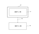
- FIG. 1 is a block diagram illustrating an outline of an overall configuration of a photodetector according to a first embodiment of the present technology.
- 3 is a diagram illustrating a photon detection unit in a pixel circuit of a photodetection device according to the first embodiment of the present technology;
- FIG. 5A to 5C are diagrams illustrating an example of an operation of the light detection device according to the first embodiment of the present technology;
- 1 is a plan view illustrating a first arrangement example of a holding array unit of a light detection device according to a first embodiment of the present technology;
- 1 is a plan view illustrating an arrangement example 2 of a holding array unit of a light detection device according to a first embodiment of the present technology;
- FIG. 11 is an exploded perspective view illustrating an arrangement example 3 of a holding array unit of a light detection device according to a first embodiment of the present technology
- FIG. 10 is a diagram illustrating a schematic configuration of a pixel unit according to Example 1 of a photodetector according to a second embodiment of the present technology
- FIG. 13 is a diagram illustrating a schematic configuration of a pixel unit according to Example 2 of a photodetector according to a second embodiment of the present technology
- FIG. 13 is a diagram illustrating a schematic configuration of a pixel unit according to Example 3 of a photodetector according to a second embodiment of the present technology.
- FIG. 10 is a diagram illustrating a schematic configuration of a pixel unit according to Example 1 of a photodetector according to a second embodiment of the present technology
- FIG. 13 is a diagram illustrating a schematic configuration of a pixel unit according to Example 2 of a photodetector according to a second embodiment of the present technology
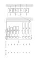
- FIG. 13 is a diagram illustrating a schematic configuration of a main part of a light detection device according to a third embodiment of the present technology.
- FIG. 13 is a timing chart illustrating an operation of a main part of a light detection device according to a third embodiment of the present technology.
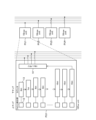
- 13 is a diagram illustrating a schematic configuration of a main part of a light detection device according to a fourth embodiment of the present technology.
- FIG. 13 is a timing chart illustrating an operation of a main part of a light detection device according to a fourth embodiment of the present technology.
- 13 is a circuit diagram showing a first circuit configuration example of a retention array unit according to a fifth embodiment of the present technology; FIG.
- FIG. 13 is a circuit diagram showing a second circuit configuration example of a retention array unit according to a fifth embodiment of the present technology
- FIG. 13 is a circuit diagram showing an example of a circuit configuration of a pixel array unit and a retention array unit according to a sixth embodiment of the present technology.
- FIG. 23 is a diagram showing a relationship of a count value CNT to a pixel row rou in the sixth embodiment of the present technology.
- FIG. 13 is a circuit diagram showing an example of a circuit configuration of a pixel array unit and a retention array unit according to a seventh embodiment of the present technology.
- FIG. 23 is a diagram showing a relationship of a count value CNT to a pixel row rou in the seventh embodiment of the present technology.
- FIG. 1 is a diagram showing an example of a schematic configuration of a biological sample analyzer according to an application example of the present technology.
- First embodiment (example of TDI processing performed by providing a retention array unit outside a pixel array unit) 2.
- Second embodiment Example of a specific configuration of a pixel unit performing TDI processing) 3.
- Third embodiment an example in which a readout holding circuit is provided for each pixel circuit, and the held value of the holding circuit is read out to a readout line common to each pixel unit) 4.
- Fourth embodiment an example in which a readout holding circuit is provided for each pixel circuit, and the value held in the holding circuit is parallel-serial converted and read out to a readout line) 5.
- First embodiment [Configuration example of a light detection device] 1 is a block diagram showing a schematic overview of an overall configuration of a photodetector according to a first embodiment of the present technology.
- the photodetector 1 according to the first embodiment of the present technology includes a pixel array section 10, a retention array section 20, and a control section 30.
- the pixel array section 10 has a plurality of pixel circuits 11 that perform photoelectric conversion.
- the plurality of pixel circuits 11 are arranged in a matrix (array) in the effective pixel area of the pixel array section 10.
- the array section in which the plurality of pixel circuits 11 are arranged in an array will be referred to as the pixel array section in this specification.
- the object to be imaged (subject) moves, for example, at a constant speed in the pixel column direction relative to the pixel array section 10.
- the photodetection device 1 in the first embodiment of the present technology is a TDI sensor that can obtain high-sensitivity, low-noise image data by performing TDI processing to integrate the amount of charge while shifting the time in accordance with the moving speed of the object to be imaged under the control of the control unit 30 over the pixel array unit 10 and the storage array unit 20.
- Each of the multiple pixel circuits 11 has a photon detection unit 12 that generates a pulse signal in response to the incidence of photons, and a counter 13 that counts the pulse signal generated by the photon detection unit 12. Details of the photon detection unit 12 in the pixel circuit 11 will be described later.
- the counter 13 counts the photons that are incident on the photon detection unit 12 over a certain period of time.
- the count value of the counter 13 is also the pixel value of the pixel circuit 11.
- the count value of the counter 13 is sent (shifted) to the next-stage counter 13 as an initial value.
- the next-stage counter 13 counts the pulse signal by adding it to the initial value shifted from the previous-stage counter 13. This series of shifting and counting processes by the counter 13 in the pixel circuit 11 is also the above-mentioned TDI process.
- pixel units are configured with N stages (N is an integer) as one unit (one unit) for each pixel column of the pixel circuits 11.
- the N stages are also N rows (N lines).
- the pixel array section 10 is configured with (N ⁇ M) stages by arranging N stages of pixel units into M units (M is an integer).
- M 4, and 4 stages (4 units) of pixel units PU1 to PU4 are configured.
- each counter 13 in the multiple pixel circuits 11 has a data shift function that writes the count value of the counter 13 that belongs to the previous pixel row (line) of the same pixel column. Then, under the control of the control unit 30, each counter 13 in the multiple pixel circuits 11 performs TDI processing (TDI operation) as follows.
- the second stage counter 13 After the first stage counter 13 counts the pulse signal generated by the photon detection unit 12, the second stage counter 13 writes the count value of the first stage counter 13 as an initial value, and adds the pulse signal generated by the photon detection unit 12 to this initial value to obtain the count value of the second stage counter 13.
- the third stage counter 13 writes the count value of the second stage counter 13 as an initial value, and adds the pulse signal generated by the photon detection unit 12 to this initial value to obtain the count value of the third stage counter 13.
- the fourth stage counter 13 writes the count value of the third stage counter 13 as an initial value, and adds the pulse signal generated by the photon detection unit 12 to this initial value to obtain the count value of the fourth stage counter 13.
- the count values of the counters 13 in the final stage (in this example, the fourth stage) of the four pixel units PU1 to PU4 are read out through read lines L1 to L4 to the holding array section 20 arranged outside the pixel array section 10 for each pixel unit of the four pixel units PU1 to PU4 under the control of the control section 30.
- the retention array unit 20 is provided outside the pixel array unit 10 and has a plurality of retention units (retention circuits) arranged in a matrix (array).
- a retention array unit an array unit in which a plurality of retention units (retention circuits) are arranged in an array will be referred to as a retention array unit.
- the holding array section 20 under the control of the control section 30, holds the count values of the counter 13 read out through the readout lines L1 to L4 for each of the four pixel units PU1 to PU4 from the pixel array section 10.
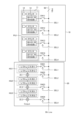
- the holding array section 20 is composed of (M-1) stages of holding units and adder circuits, in this example, three stages of holding units HU1 to HU3 and three stages of adder circuits 22_1 to 22_3.
- Each of the three stages of holding units HU1 to HU3 has N stages, in this example four stages of holding units 21_1 to 21_4, that hold the count value of the counter 13 read from one pixel unit of the four stages of pixel units PU1 to PU4 in the pixel array section 10.
- the holding units 21_1 to 21_4 have the function of shifting the held value under the control of the control unit 30.
- the three stages of addition circuits 22_1 to 22_3 perform a process of adding the held value of the last stage holding unit 21_4 in the four stages of holding units 21_1 to 21_4 to the count value of the counter 13 read from the pixel unit in the stage next to one of the four stages of pixel units PU1 to PU4 in the pixel array section 10.
- the first holding unit HU1 receives as input the count value of the counter 13 output from the first-stage pixel unit PU1 of the pixel array section 10.
- the output of the first holding unit HU1 and the output of the second-stage pixel unit PU2 of the pixel array section 10 are then added together in the first-stage adder circuit 22_1, and the result of this addition becomes the input to the second holding unit HU2.
- the output of the second holding unit HU2 and the output of the third pixel unit PU3 in the pixel array section 10 are added in the second-stage adder circuit 22_2, and the result of this addition becomes the input to the third holding unit HU3.
- the output of the third holding unit HU3 and the output of the fourth-stage pixel unit PU4 in the pixel array section 10 are added in the third-stage adder circuit 22_3, and the result of this addition is obtained as the total count value.
- the shift operation of the pixel units PU1 to PU4 in the pixel array section 10 and the shift operation of the holding units HU1 to HU3 in the holding array section 20 are performed at the same timing.
- the control unit 30 appropriately supplies control signals including a shift clock to each of the four stages of pixel units PU1 to PU4 in the pixel array unit 10 and the three stages of holding units HU1 to HU3 in the holding array unit 20.
- the control unit 30 then performs a shift operation to write the count value of the previous stage counter to the next stage counter before starting exposure of the next line in the pixel unit, and controls the pixel array unit 10 to read out the count value of the counter 13 for each of the four stages of pixel units PU1 to PU4 to the holding array unit 20.
- FIG. 2 is a diagram for explaining the photon detection unit 12 in the pixel circuit 11.
- a in Fig. 2 is a circuit diagram showing an example of the circuit configuration of the photon detection unit 12.
- the photon detection unit 12 has, for example, a light receiving unit 121, a quenching unit 122, and a waveform shaping unit 123.
- a reset pulse RST is given to the photon detection unit 12 from a recharge control unit 120 which is an external circuit.
- the light receiving unit 121 may be an avalanche photodiode (APD).
- APD avalanche photodiode
- An avalanche photodiode that multiplies a single photon by the avalanche phenomenon is called a single photon avalanche diode (SPAD (Single Photon Avalanche Diode)).
- SPAD Single Photon Avalanche Diode
- a resistive element for example, may be used instead of the quench unit 122.
- the quench unit 122 has a function of stopping the avalanche phenomenon (quench function) by lowering the voltage applied to the light receiving unit 121 to the breakdown voltage.
- the quench unit 122 further has a function of making the light receiving unit 121 detect photons again by making the voltage applied to the light receiving unit 121 a bias voltage equal to or higher than the breakdown voltage.
- the quench unit 122 is configured of, for example, a P-type MOS (Metal Oxide Semiconductor) transistor, and is connected between the node of the power supply voltage V DD and the light receiving unit 121 (specifically, the cathode electrode of the SPAD element) to recharge the light receiving unit 121.
- P-type MOS Metal Oxide Semiconductor
- a reset pulse RST is applied to the gate electrode of the P-type MOS transistor that constitutes the quench section 122 from the recharge control section 120, which is an external circuit.
- This reset pulse RST is a recharge pulse for controlling the timing of recharging the light receiving section 121.
- the waveform shaping unit 123 is composed of, for example, a CMOS inverter, and performs waveform shaping on the output of the light receiving unit 121, i.e., the cathode voltage Vk of the P-type MOS transistor, and outputs it as a pulse signal PLS.
- the photon detection unit 12 is configured to periodically reset the light receiving unit 121 by a reset pulse RST provided by the recharge control unit 120, which is an external circuit. This makes it possible to control the counter 13 to a maximum count number according to the number of bits.
- B in Figure 2 is a timing chart showing the timing relationship between the cathode voltage Vk of the P-type MOS transistor, the reset pulse RST, and the pulse signal PLS.
- Fig. 3 is a diagram for explaining an example of the operation of the photodetection device 1 in the first embodiment.
- Fig. 3 illustrates an example of the operation of four stages (four units) of pixel units PU1 to PU4, three stages of holding units HU1 to HU3, and three stages of addition circuits 22_1 to 22_3 in one pixel column.
- Steps 1 to 4 When the shift operation in the pixel array section 10 reaches the Nth stage (fourth stage in this example) of the first pixel unit PU1 (Steps 1 to 4), at the next shift timing, the count value of the counter 13 in the fourth stage of the first pixel unit PU1 is shifted to the first stage holding section 21_1 of the first holding unit HU1 in the holding array section 20 (Step 5). At the same time, a new count operation is started in the first stage of the second pixel unit PU2.
- a shift operation is also performed in holding unit HU1, the first unit in holding array section 20 (Steps 6 to 8). Then, when the shift operation reaches the fourth stage, at the next shift timing, the count value of the fourth stage of pixel unit PU2, the second unit in pixel array section 10, and the held value of the fourth stage of holding unit HU1, the first unit in holding array section 20 are added, and the added value is held in the next holding unit, that is, the first stage of holding unit HU2, the second unit (Step 9). At the same time, a new count operation is started in the first stage of pixel unit PU3, the third unit in pixel array section 10.
- a shift operation is also performed in holding unit HU2, the second unit in holding array section 20 (Steps 10-12). Then, when the shift operation reaches the fourth stage, at the next shift timing, the count value of the fourth stage of pixel unit PU3, the third unit in pixel array section 10, is added to the held value of the fourth stage of holding unit HU2, the second unit in holding array section 20, and the added value is held in the next holding unit, that is, the first stage of holding unit HU3, the third unit (Step 13). At the same time, a new count operation is started in the first stage of pixel unit PU4, the fourth unit in pixel array section 10.
- Steps 14 to 16 a shift operation is also performed in the third holding unit HU3 in the holding array section 20 (Steps 14 to 16). Then, when the shift operation reaches the fourth stage, at the timing of the next shift, the fourth stage count value of the fourth pixel unit PU4 in the pixel array section 10 and the held value of the fourth stage of the third holding unit HU3 in the holding array section 20 are added together, and the added value is output as the total count value.
- the above-mentioned series of processes i.e., the process of repeatedly reading the count value of the counter 13 for every N stages to the external storage array unit 20 of the pixel array unit 10 and shifting and adding in the external storage array unit 20, is the TDI process executed in the photodetector 1 in the first embodiment of the present technology.
- the holding array section 20 is provided outside the pixel array section 10, and the count value of the counter 13 is read out to the holding array section 20 for shifting and addition every N stages, thereby reducing the circuit area within the pixel array section 10. Furthermore, by reducing the circuit area, the TDI process can be made multi-staged, and the total count value (total number of counts) can be increased accordingly, thereby expanding the dynamic range.
- Example of storage array arrangement Next, an example of the arrangement of the retention array section 20 of the light detection device 1 in the first embodiment of the present technology will be described.
- the example of the arrangement of the retention array section 20 is the same in each embodiment described later.
- an example of the arrangement 1, an example of the arrangement 2, and an example of the arrangement 3 will be described, but it is arbitrary which example of the arrangement is adopted.
- FIG. 4 is a plan view showing a schematic arrangement example 1 of the retention array section 20 of the photodetector 1 according to the first embodiment of the present technology.
- a pixel array section 10 in which a plurality of pixel circuits 11 are arranged in an array is formed on a semiconductor substrate 101.
- the semiconductor substrate 101 on which the pixel array section 10 is formed is a sensor chip.
- the pixel array section 10 is formed in the semiconductor substrate 101, whereas the retention array section 20 is arranged outside the semiconductor substrate 101.
- the pixel array section 10 arranged in the semiconductor substrate 101 and the retention array section 20 arranged outside the semiconductor substrate 101 are electrically connected through a multi-bit readout line 102.
- (Layout example 2) 5 is a plan view showing a schematic arrangement example 2 of the retention array section 20 of the photodetector 1 according to the first embodiment of the present technology.
- the pixel array section 10 in which a plurality of pixel circuits 11 are arranged in an array is formed on a semiconductor substrate 101, and the retention array section 20 is formed on the same semiconductor substrate 101.
- the pixel array section 10 and the retention array section 20 are electrically connected through a readout line 102. In this way, by arranging the retention array section 20 on the same semiconductor substrate 101 as the pixel array section 10, the electrical connection of the retention array section 20 to the pixel array section 10 is facilitated.
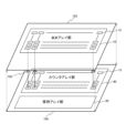
- (Layout example 3) 6 is an exploded perspective view illustrating an arrangement example 3 of the retention array unit 20 of the light detection device 1 according to the first embodiment of the present technology.
- the arrangement example 3 is an arrangement example in a stacked chip structure in which at least two semiconductor substrates are stacked.
- a two-layer stacked chip structure is formed in which a first semiconductor substrate 103 and a second semiconductor substrate 104 are stacked.
- a pixel array section 10 excluding each counter 13 of a plurality of pixel circuits 11 is formed on the first semiconductor substrate 103 in the upper layer
- a counter array section 40 in which each counter 13 of a plurality of pixel circuits 11 is arranged in an array and a retention array section 20 are formed on the second semiconductor substrate 104 in the lower layer.
- the upper first semiconductor substrate 103 on which the pixel array section 10 is formed is a sensor chip
- the lower second semiconductor substrate 104 on which the counter array section 40 and the retention array section 20 are formed is a logic chip.
- Each photon detection section 12 of the pixel array section 10 on the upper sensor chip and each counter 13 of the counter array section 40 on the lower logic chip are electrically connected via a connection section 105 such as a Cu-Cu connection (bond), a through silicon via (TSV), or a microbump.
- the photon detection unit 12 in the pixel array unit 10 is disposed on the upper first semiconductor substrate 103, and the counter array unit 40 and the holding array unit 20 in the pixel array unit 10 are disposed on the lower second semiconductor substrate 104, which facilitates electrical connection between each counter 13 in the counter array unit 40 and the holding array unit 20.
- the pixel array section 10 excluding each counter 13 of the multiple pixel circuits 11 is formed on the first semiconductor substrate 103 of the first layer, but as in Arrangement Example 1, the pixel array section 10 including each counter 13 of the multiple pixel circuits 11 may be formed.
- Second embodiment of the present technology is an example of a specific configuration of a pixel unit that performs TDI processing. Note that the overall configuration of the photodetector 1 is similar to that of the first embodiment described above, and therefore a detailed description thereof will be omitted. This also applies to each of the embodiments described below.
- Example 1 is an example in which the number of bits of counter 13 in each stage in each pixel unit is set based on the maximum value of the count value (count number) of counter 13 in the first stage and the number of stages in one unit.
- Fig. 7 is a diagram illustrating a schematic configuration of a pixel unit according to Example 1 of a photodetector according to a second embodiment of the present technology.
- the maximum count value per period is 63 and a 6-bit counter is placed as the first stage counter
- the number of bits of the counter 13 in each stage in one unit is set to the maximum count value of the counter 13 in the first stage times the number of stages N in one unit, so that one unit can be formed in a smaller area.
- Example 2 is an example in which at least one readout holding circuit is provided in each pixel unit.
- Fig. 8 is a diagram illustrating a configuration of a pixel unit according to Example 2 of a photodetector according to a second embodiment of the present technology.
- the pixel unit PU1 has at least one memory 14 as a readout holding circuit within the pixel unit.
- the count value of the counter 13 in the Nth stage is held in the memory 14.
- the count value held in the memory 14 is read out to the holding array section 20 under the control of the control section 30.
- the first-stage pixel unit PU1 as an example to explain providing at least one readout hold circuit within the pixel unit, but the second-stage to fourth-stage pixel units PU2-PU4 are similar to the first-stage pixel unit PU1.
- the pixel unit according to the second embodiment is configured to have at least one memory 14 as a readout holding circuit within each pixel unit. This allows the readout time to be secured since it is sufficient to complete the readout of the count value held in the memory 14 during the exposure period in which the shift operation is performed in each stage. As a result, it is also possible to accommodate an increased number of pixel units.
- Example 3 is an example in which each pixel unit has a blanking photon detection unit that does not perform exposure and a corresponding readout holding circuit.
- Fig. 9 is a diagram showing a schematic configuration of a pixel unit according to Example 3 of a photodetection device according to a second embodiment of the present technology.
- the pixel unit PU1 has a configuration including a blanking photon detection section 15 that does not perform exposure as the pixel circuit of the final stage (Nth stage) and a memory 16 that serves as a corresponding readout holding circuit.
- the count value held in the memory 16 is read out to the holding array section 20 during the exposure period under the control of the control section 30 without performing exposure.
- the first-stage pixel unit PU1 As an example and explained how the final-stage pixel circuit is provided with a blanking photon detection unit 15 that does not perform exposure and a corresponding readout holding circuit, but the second-stage to fourth-stage pixel units PU2 to PU4 are similar to the first-stage pixel unit PU1.
- a blanking photon detection unit 15 and a readout holding circuit are provided as the pixel circuit of the final stage in each pixel unit, making the layout of each pixel unit easier than in the second embodiment. Furthermore, since it is only necessary to complete the reading of the count value held in the readout holding circuit during the exposure period in which shifting is performed in each stage, it is possible to ensure the readout time.
- the third embodiment of the present technology is an example in which a readout hold circuit is provided for each pixel circuit of a pixel unit, and a count value (held value) held in the hold circuit is read out to a readout line common to each pixel unit by a switch element.
- FIG. 10 is a diagram showing a schematic configuration of the main parts of a photodetector in a third embodiment of the present technology.
- FIG. 10 shows an example of the main parts of the photodetector 1, specifically, the circuit configuration of pixel unit PU1 of four rows (four units) of pixel units PU1 to PU4 in the pixel array section 10, and three rows of holding units HU1 to HU3 in the holding array section 20, for one pixel column.
- the pixel circuit 11 has a readout hold circuit 17 in addition to a photon detection unit 12 and a counter 13.
- the pixel unit PU1 also has switch elements SW11 to SW14 for each pixel circuit 11.
- readout lines 50 corresponding to the number of bits of the counter 13 are wired for each pixel column.
- the readout hold circuit 17 and the readout line 50 in each pixel circuit 11 are selectively connected by switch elements SW11 to SW14 under the control of selection signals SEL1 to SEL4 provided by the control section 30.
- the first-stage holding unit HU1 is composed of two stages of shift register 11 and shift register 12.
- the second-stage holding unit HU2 is composed of two stages of shift register 21 and shift register 22.
- the third-stage holding unit HU3 is composed of two stages of shift register 31 and shift register 32.
- a switch element SW21 is provided between the input end of the shift register 11 of the first-stage holding unit HU1 and the readout line 50.
- the switch element SW21 is turned on (closed) in response to a selection signal SEL1 supplied from the control unit 30, and inputs the count value of the first-stage counter 13 of the pixel unit PU1, which is supplied through the readout line 50, to the shift register 11.
- a switch element SW22 is provided between the first-stage addition circuit 22_1 and the readout line 50.
- the switch element SW22 is turned on in response to a selection signal SEL2 supplied from the control unit 30, and inputs the count value of the second-stage counter 13 of the pixel unit PU1, which is supplied through the readout line 50, to the addition circuit 22_1.
- the addition circuit 22_1 adds the held value of the first-stage holding unit HU1 and the count value of the second-stage counter 13 of the pixel unit PU1, and the addition result is input to the second-stage holding unit HU2.
- a switch element SW23 is provided between the second-stage addition circuit 22_2 and the readout line 50.
- the switch element SW23 is turned on in response to a selection signal SEL3 supplied from the control unit 30, and inputs the count value of the third-stage counter 13 of the pixel unit PU1, which is supplied through the readout line 50, to the addition circuit 22_2.
- the addition circuit 22_2 adds the held value of the second-stage holding unit HU2 and the count value of the third-stage counter 13 of the pixel unit PU1, and the addition result is input to the third-stage holding unit HU3.
- a switch element SW24 is provided between the third-stage addition circuit 22_3 and the readout line 50.
- the switch element SW24 is supplied from the control unit 30, and turns on in response to a selection signal SEL4, thereby inputting the count value of the fourth-stage counter 13 of the pixel unit PU1, supplied through the readout line 50, to the addition circuit 22_3.
- the addition circuit 22_3 adds the held value of the third-stage holding unit HU3 and the count value of the fourth-stage counter 13 of the pixel unit PU1, and outputs the addition result as a total count value.
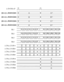
- FIG. 11 is a timing chart explaining the operation of the main parts of the photodetector in the third embodiment of the present technology.
- FIG. 11 shows the timing relationship of the shift clock and selection signals SEL1 to SEL4 provided from the control unit 30 to the pixel unit PU1 and the holding units HU1 to HU3, as well as the state of each shift register of the readout holding circuits 1 to 4 of the pixel unit PU1 and the holding units HU1 to HU3.
- the pixel units are sequentially connected to the readout line 50 by the switch elements SW11 to SW14.
- the input terminals of the hold units HU1 to HU3 corresponding to the readout hold circuits connected to the readout line 50 are connected to the readout line 50 by the switch elements SW21 to SW24, thereby sequentially reading out the held values (count values) from the readout hold circuits 1 to 4 of the pixel array section 10 to the hold array section 20.
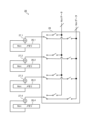
- the fourth embodiment of the present technology is an example in which a readout holding circuit is provided for each pixel circuit of a pixel unit, and a count value (held value) held in the holding circuit is parallel-serial converted and read out to a readout line.
- FIG. 12 is a diagram showing a schematic configuration of the main parts of a photodetector in a fourth embodiment of the present technology.
- FIG. 12 shows an example of the main parts of the photodetector 1, specifically, the circuit configuration of pixel unit PU1 of four rows (four units) of pixel units PU1 to PU4 in the pixel array section 10, and three rows of holding units HU1 to HU3 in the holding array section 20, for one pixel column.
- the pixel circuit 11 has a readout hold circuit 17 in addition to the photon detection unit 12 and the counter 13.
- the readout hold circuit 17 outputs the count value held by the counter 13 as, for example, 4-bit parallel data.
- the pixel unit PU1 has a parallel-serial conversion circuit 18 for each pixel circuit 11 as a subsequent circuit to the readout holding circuit 17.
- the parallel-serial conversion circuit is abbreviated as "PS.”
- readout lines BL1 to BL4 are wired for each pixel column, the number of which corresponds to the number of stages of pixel units PU1.
- the parallel-serial conversion circuit 18 corresponding to each pixel circuit 11 converts the parallel data output from the readout hold circuit 17 into serial data and outputs it to the corresponding readout lines BL1 to BL4.
- the first-stage holding unit HU1 is composed of a two-stage shift register 1212.
- the second-stage holding unit HU2 is composed of two-stage shift registers 21 and 22.
- the third-stage holding unit HU3 is composed of two-stage shift registers 31 and 32.
- a serial-parallel conversion circuit 23_1 is disposed between the input terminal of the shift register 11 of the first-stage holding unit HU1 and the readout line BL1.
- the serial-parallel conversion circuit is abbreviated as "SP.”
- the serial-parallel conversion circuit 23_1 converts serial data regarding the count value of the first-stage counter 13 of the pixel unit PU1, which is supplied via the readout line BL1, into parallel data and inputs it to the shift register 11.
- a serial-parallel conversion circuit 23_2 is disposed between the first-stage addition circuit 22_1 and the readout line BL2.
- the serial-parallel conversion circuit 23_2 converts serial data for the count value of the second-stage counter 13 of the pixel unit PU1, which is supplied through the readout line BL2, into parallel data and inputs it to the addition circuit 22_1.
- the addition circuit 22_1 adds the held value of the first-stage holding unit HU1 and the count value of the second-stage counter 13 of the pixel unit PU1, and the addition result is input to the second-stage holding unit HU2.
- a serial-parallel conversion circuit 23_3 is disposed between the second-stage addition circuit 22_2 and the readout line BL3.
- the serial-parallel conversion circuit 23_3 converts serial data for the count value of the third-stage counter 13 of the pixel unit PU1, which is supplied through the readout line BL3, into parallel data and inputs it to the addition circuit 22_2.
- the addition circuit 22_2 adds the held value of the second-stage holding unit HU2 and the count value of the third-stage counter 13 of the pixel unit PU1, and the addition result is input to the third-stage holding unit HU3.
- a serial-parallel conversion circuit 23_4 is disposed between the third-stage addition circuit 22_3 and the readout line BL4.
- the serial-parallel conversion circuit 23_4 converts the serial data for the count value of the fourth-stage counter 13 of the pixel unit PU1, which is supplied through the readout line BL4, into parallel data and inputs it to the addition circuit 22_3.
- the addition circuit 22_3 adds the held value of the third-stage holding unit HU3 and the count value of the fourth-stage counter 13 of the pixel unit PU1, and outputs the addition result as a total count value.
- FIG. 13 is a timing chart explaining the operation of the main parts of the photodetector in the fourth embodiment of the present technology.
- FIG. 13 shows the states of the readout hold circuits 1-4 of pixel unit PU1, the data on readout lines BL1-BL4, and the shift registers of the hold units HU1-HU3 in response to the shift clock provided from the control unit 30 to pixel unit PU1 and hold units HU1-HU3.
- the count values (held values) held in the readout holding circuits provided for each pixel circuit of the pixel unit are parallel-serial converted and read out to the readout line, so that only one readout line is required for each pixel unit, thereby reducing the number of readout lines.
- the fifth embodiment of the present technology is an example of another circuit configuration of the holding array unit 20.
- two circuit configuration examples, a circuit configuration example 1 and a circuit configuration example 2 will be described as examples of the other circuit configuration of the holding array unit 20.
- Fig. 14 is a circuit diagram showing a first circuit configuration example of the holding array unit 20 according to the fifth embodiment of the present technology.
- the holding units are arranged in N stages (Row1 to RowN), and the data (count value) input from the pixel array unit 10 is 4-bit data (A_D1 to A_D4).
- circuit configuration of the holding unit of the column to which data A_D1 is input but the circuit configuration of the holding units of the columns to which data A_D2 to A_D4 are input is the same as the circuit configuration of the holding unit of the column to which data A_D1 is input.
- the holding unit of the column to which data A_D1 is input is composed of N stages of D-type flip-flops 24_1 to 24_N and an adder circuit 25.
- the D-type flip-flop 24_1 receives data A_D1 input from the pixel array section 10 as its D input.
- the D-type flip-flops 24_1 to 24_N configure a shift register by using the Q output as the D input of the next stage, and perform shift operations at the same timing as the shift operations in the pixel array section 10, in synchronization with the shift clock provided by the control section 30 shown in FIG. 1.
- the addition circuit 25 adds the Q output of the N-1th stage D-type flip-flop (not shown) to the data B_D supplied from the pixel array unit 10, and supplies the result of this addition to the D input of the final stage D-type flip-flop 24_N.
- the holding array unit 20 according to the circuit configuration example 1 of the circuit configuration described above can also shift and add to the count value of the counter 13 read from the pixel array unit 10, in the same manner as the holding array unit 20 in the first embodiment.
- Fig. 15 is a circuit diagram showing a second circuit configuration example of the holding array section 20 according to the fifth embodiment of the present technology.
- Fig. 15 illustrates one holding unit having an N-stage (four stages in this example) configuration.
- the storage unit is composed of N-bit memories 26-1 to 26-4, addition circuits 27-1 to 27-4, and a multiplexer 28.
- memories 26-1 to 26-4 are selected in sequence in synchronization with the shift of the readout row (line) of the pixel unit, so that data is stored in a different memory at each time.
- the output (count value) of the first pixel unit is held, and then after a period of N-stage shift operation, the output of the second pixel unit is taken in and added to the previously held value by the adder circuit 27-1, and the added value is held. This allows for driving equivalent to the shift operation of the holding array section 20 in the first embodiment.
- the holding array unit 20 according to the circuit configuration example 2 of the circuit configuration described above can also shift and add to the count value of the counter 13 read from the pixel array unit 10, in the same manner as the holding array unit 20 in the first embodiment.
- the sixth embodiment of the present technology is an example in which the count value of the most significant bit (MSB) of one pixel unit is read out to the outside, and the count values of the remaining bits are sent to a counter in the next stage.
- MSB most significant bit
- FIG. 16 is a circuit diagram showing an example of the circuit configuration of the pixel array section 10 and the holding array section 20 in the sixth embodiment of the present technology.
- the count value of the most significant bit (MSB) from one pixel unit is read out to the outside, and the remaining bits are sent to the pixel unit (counter) of the next stage.
- one pixel unit may be provided with a readout holding circuit that holds the count value of the most significant bit, and the count value of the most significant bit may be read out from the holding circuit.
- the count value of the final stage of each pixel unit, other than the most significant bit that was read out, is shifted to the first stage counter of the next pixel unit, and TDI processing (TDI operation) is performed continuously from the shifted value.
- the most significant bit count value read from the pixel array section 10 is shifted by the most significant bit holding sections 29_1 to 29_8. Then, in the addition circuit 22_1, it is added to the most significant bit count value read from the pixel unit of the next stage, and the result is input to the holding unit of the next stage.
- the above operation causes the holding array unit 20 to perform an operation equivalent to counting the most significant bit. Then, in the final stage, the count value of the lower bits read out from the pixel array unit 10 and the count value of the most significant bit shifted in the holding array unit 20 are added together in the adder circuit 22_1 to obtain a total count value.
- FIG. 17 is a diagram showing the relationship of the count value CNT to the pixel row rou in the sixth embodiment of the present technology.
- a shows the relationship of the count value CNT to the pixel row rou in the pixel array unit 10
- b in the same figure shows the relationship of the count value CNT to the pixel row rou in the holding array unit 20.
- the most significant bit of one pixel unit in the pixel array section 10 is read out to the holding array section 20, and the remaining bits are sent to the counter of the pixel unit of the next stage. Then, in the holding array section 20, a process is performed to obtain a total count value from the count value of the most significant bit counted in the holding unit and the value of the lower bits shifted to the pixel unit of the next stage. This basically makes it possible to execute the same TDI process as in the first embodiment. Furthermore, according to the sixth embodiment, it is possible to reduce the number of bits read out from the pixel array section 10 and reduce the circuitry of the holding array section 20.
- the seventh embodiment of the present technology is an example in which the count value of the most significant bit of one pixel unit is read out to the outside, and the count values of all bits are sent to a counter in the next stage.
- FIG. 18 is a circuit diagram showing an example of the circuit configuration of the pixel array section 10 and the holding array section 20 in the seventh embodiment of the present technology.
- the holding array section 20 is arranged with 8 stages of holding sections 29_1 to 29_8 for the most significant bit of 1 bit.
- the holding array section 20 is further arranged with an overflow determination circuit 61 and holding sections 62_1 to 62_8 for 3-bit overflow count.
- the count value of the most significant bit (MSB) from one pixel unit is read out to the outside, and the remaining bits are sent to the pixel unit (counter) of the next stage.
- one pixel unit may be provided with a readout holding circuit that holds the count value of the most significant bit, and the count value of the most significant bit may be read out from the holding circuit.
- the final count value of each pixel unit is shifted directly to the first counter of the next pixel unit, and TDI processing (TDI operation) is performed continuously from the shifted value.
- the overflow count holding sections 62_1 to 62_8 also perform a shift operation in the same way as the most significant bit holding sections 29_1 to 29_8.
- the holding array unit 20 performs an operation equivalent to counting the upper bits. Then, in the final stage, the count value of the lower bits read out from the pixel array unit 10 and the count value of the upper bits counted by the holding array unit 20 are added together to obtain a total count value.
- FIG. 19 is a diagram showing the relationship of the count value CNT to the pixel row rou in the seventh embodiment of the present technology.
- a shows the relationship of the count value CNT to the pixel row rou in the pixel array unit 10
- b in the same figure shows the relationship of the count value CNT to the pixel row rou in the holding array unit 20.
- the seventh embodiment of the present technology in the pixel array section 10, the most significant bit of one pixel unit is read out to the holding array section 20, and all bits are sent to the counter of the pixel unit of the next stage. Then, in the holding array section 20, overflow of the most significant bit is detected, and a total count value is obtained from the number of times the overflow is detected and the value of the lower bits shifted to the pixel unit of the next stage.
- This basically makes it possible to execute the same TDI processing as in the first embodiment.
- Application Examples> 20 is a diagram showing a schematic configuration example of a biological sample analyzer 200 according to an application example of the present technology.
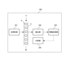
- the biological sample analyzer 200 is an example of an electronic device of the present technology.
- the light detection device 1 of the present technology can be used in a detection unit 202, which will be described later, in the biological sample analyzer 200.
- the biological sample analyzer 200 includes a light irradiation unit 201 that irradiates light onto the biological sample S flowing through the flow path C, a detection unit 202 that detects the light generated by irradiating the biological sample S with light, and an information processing unit 203 that processes information related to the light detected by the detection unit 202.
- the biological sample analyzer 200 examples include a flow cytometer and an imaging cytometer.
- the biological sample analyzer 200 may include a sorting section 204 that sorts specific biological particles P from within the biological sample S.
- An example of a biological sample analyzer 200 that includes a sorting section 204 is a cell sorter.
- the biological sample S may be a liquid sample containing biological particles P.
- the biological particles P are, for example, cells or non-cellular biological particles.
- the cells may be living cells, and more specific examples include blood cells such as red blood cells and white blood cells, and reproductive cells such as sperm and fertilized eggs.
- the cells may be directly collected from a specimen such as whole blood, or may be cultured cells obtained after culture.
- Examples of the non-cellular biological particles include extracellular vesicles, particularly exosomes and microvesicles.
- the biological particles P may be labeled with one or more labeling substances (e.g., dyes (particularly fluorescent dyes) and fluorescent dye-labeled antibodies, etc.).
- the biological sample analyzer of the present technology may analyze particles other than the biological particles P, and beads, etc. may be analyzed for calibration, etc.
- the flow channel C is configured to allow the biological sample S to flow.
- the flow channel C can be configured to form a flow in which the biological particles P contained in the biological sample S are arranged in a substantially straight line.
- the flow channel structure including the flow channel C may be designed to form a laminar flow.
- the flow channel structure is designed to form a laminar flow in which the flow (sample flow) of the biological sample S is surrounded by the flow of the sheath liquid.
- the design of the flow channel structure may be appropriately selected by a person skilled in the art, and a known design may be adopted.
- the flow channel C may be formed in a flow channel structure such as a microchip (a chip having a flow channel on the order of micrometers) or a flow cell.
- the width of the flow channel C may be 1 mm or less, and in particular, 10 ⁇ m or more and 1 mm or less.
- the flow channel C and the flow channel structure including the flow channel C may be formed from a material such as plastic or glass
- the biological sample analysis device 200 is configured so that the biological sample S flowing in the flow path C, and in particular the biological particles P in the biological sample S, is irradiated with light from the light irradiation unit 201.
- the biological sample analysis device 200 may be configured so that the interrogation point of light on the biological sample S is in the flow path structure in which the flow path C is formed, or the interrogation point of light may be configured so that it is outside the flow path structure.
- An example of the former is a configuration in which the light is irradiated onto the flow path C in a microchip or flow cell. In the latter, the light may be irradiated onto the biological particles P after they have left the flow path structure (in particular its nozzle portion), and an example of this is a jet-in-air type flow cytometer.
- the light irradiation unit 201 includes a light source unit that emits light and a light guide optical system that guides the light to an irradiation point.
- the light source unit includes one or more light sources.
- the type of light source is, for example, a laser light source or an LED.
- the wavelength of the light emitted from each light source may be any of ultraviolet light, visible light, and infrared light.
- the light guide optical system includes optical components such as a beam splitter group, a mirror group, or an optical fiber.
- the light guide optical system may also include a lens group for collecting light, including, for example, an objective lens. There may be one or more irradiation points where the biological sample and the light intersect.
- the light irradiation unit 201 may be configured to collect light irradiated from one or more different light sources to one irradiation point.
- the detection unit 202 includes at least one photodetector that detects light generated by irradiating the bioparticle P with light.
- the light to be detected is, for example, fluorescence or scattered light (for example, one or more of forward scattered light, back scattered light, and side scattered light).
- Each photodetector includes one or more light receiving elements, and has, for example, a light receiving element array.
- Each photodetector may include, as a light receiving element, one or more PMTs (photomultiplier tubes) and/or photodiodes such as APDs and MPPCs.
- the photodetector includes, for example, a PMT array in which a plurality of PMTs are arranged in a one-dimensional direction.
- the detection unit 202 may also include an imaging element such as a CCD or CMOS.
- the detection unit 202 can acquire an image of the bioparticle P (for example, a bright field image, a dark field image, and a fluorescent image) using the imaging element.
- the detection unit 202 includes a detection optical system that allows light of a predetermined detection wavelength to reach a corresponding photodetector.
- the detection optical system includes a spectroscopic section such as a prism or a diffraction grating, or a wavelength separation section such as a dichroic mirror or an optical filter.
- the detection optical system is configured to, for example, disperse light generated by irradiating light onto a bioparticle P, and detect the dispersed light by a number of photodetectors greater than the number of fluorescent dyes with which the bioparticle P is labeled.
- a flow cytometer that includes such a detection optical system is called a spectral flow cytometer.
- the detection optical system is also configured to, for example, separate light corresponding to the fluorescent wavelength range of a specific fluorescent dye from the light generated by irradiating light onto a bioparticle P, and detect the separated light by a corresponding photodetector.
- the detection unit 202 may also include a signal processing unit that converts the electrical signal obtained by the photodetector into a digital signal.
- the signal processing unit may include an A/D converter as a device that performs the conversion.
- the digital signal obtained by the conversion by the signal processing unit may be transmitted to the information processing unit 203.
- the digital signal may be treated by the information processing unit 203 as data related to light (hereinafter also referred to as "light data").
- the light data may be light data including, for example, fluorescent light data. More specifically, the light data may be light intensity data, and the light intensity may be light intensity data of light including fluorescent light (which may include feature quantities such as Area, Height, Width, etc.).
- the information processing unit 203 includes, for example, a processing unit that executes processing of various data (e.g., optical data) and a storage unit that stores various data.
- various data e.g., optical data
- the processing unit can perform a fluorescence leakage correction (compensation process) on the light intensity data.
- the processing unit executes a fluorescence separation process on the optical data to acquire the light intensity data corresponding to the fluorescent dye.
- the above-mentioned fluorescence separation process may be performed according to the unmixing method described in, for example, JP 2012232259 A.
- the processing unit may acquire morphological information of the bioparticles based on an image acquired by the image sensor.
- the memory unit may be configured to store the acquired optical data.
- the memory unit may further be configured to store spectral reference data used in the above-mentioned unmixing process.
- the information processing unit 203 can execute a judgment as to whether to fractionate the biological particles P based on the optical data and/or morphological information. Then, the information processing unit 203 can control the fractionation unit 204 based on the result of the judgment, and the fractionation unit 204 can fractionate the biological particles P.
- the information processing unit 203 may be configured to be able to output various data (e.g., optical data and images). For example, the information processing unit 203 may output various data (e.g., two-dimensional plots, spectral plots, etc.) generated based on the optical data. The information processing unit 203 may also be configured to be able to accept input of various data, for example, accepting gating processing on a plot by a user.
- the information processing unit 203 may include an output unit (e.g., a display, etc.) or an input unit (e.g., a keyboard, etc.) for executing the output or input.
- the information processing unit 203 may be configured as a general-purpose computer, for example, as an information processing device equipped with a CPU, RAM, and ROM.
- the information processing unit 203 may be included in a housing in which the light irradiation unit 201 and the detection unit 202 are equipped, or may be located outside the housing.
- various processes or functions by the information processing unit 203 may be realized by a server computer or cloud connected via a network.
- the sorting unit 204 executes sorting of the bioparticles P according to the determination result by the information processing unit 203.
- the sorting method may be a method of generating droplets containing bioparticles by vibration, applying an electric charge to the droplets to be sorted, and controlling the traveling direction of the droplets by electrodes.
- the sorting method may be a method of controlling the traveling direction of the bioparticles P in the flow path structure and sorting.
- the flow path structure is provided with, for example, a control mechanism using pressure (spray or suction) or electric charge.
- An example of the flow path structure is a chip (for example, a chip described in JP 2020-76736 A) having a flow path structure in which the flow path C branches into a recovery flow path and a waste liquid flow path downstream, and specific bioparticles are collected into the recovery flow path.
- the biological sample analyzer 200 was used as an example of an electronic device of the present technology, but the electronic device of the present technology is not limited to the biological sample analyzer 200.
- the present technology can also be configured as follows. (1) a pixel array section in which pixel circuits, each having a photon detection section that generates a pulse signal in response to incidence of a photon and a counter that counts the pulse signal generated by the photon detection section, are arranged in a matrix, and N stages (N is an integer) of the pixel circuits are arranged as one unit for each pixel column to constitute a pixel unit; a holding array unit provided outside the pixel array unit and holding the count value of the counter read from the pixel unit; a control unit that performs a shift operation to write a count value of the counter in a previous stage to the counter in a next stage before exposure of a next line is started in the pixel unit, and reads out the count value of the counter for each pixel unit from the pixel array unit to the retention array unit in units of M pixel units (M is an integer),
- the storage array unit includes: (M-1) holding units each having N stages of holding units that are provided corresponding to
- Each pixel unit of the M pixel units includes a readout holding circuit that holds a count value of the counter read out under the control of the control unit, The light detection device according to (1), wherein the control unit sequentially reads out the count value of the counter from the readout holding circuit.
- Each pixel unit of the M pixel units has a parallel-serial conversion unit that performs parallel-serial conversion on the count value of the counter held in the holding array unit, The photodetector according to (3), wherein the control unit performs control to read out the values parallel-to-serial converted by the parallel-to-serial conversion unit to the corresponding readout lines.
- Each pixel unit of the M pixel units has, as the pixel circuit in a final stage, a blanking photon detection unit that does not perform exposure and a readout holding circuit, The photodetector according to (1), wherein the control unit controls reading out the count value held in the readout holding circuit to the holding array unit. (7) The photodetector according to (1), wherein the N-stage holding sections in the holding unit are made of shift registers and perform a shift operation at the same timing as a shift operation in the pixel unit.
- the holding unit includes an N-stage memory and a multiplexer for selecting one of the N-stage memories;
- Photodetection device 10 Pixel array section 11_1 to 11_8 Pixel circuit 12 Photon detection section 13 Counter 14, 16, 26_1 to 26_4 Memory 15 Blanking photon detection section 17 Readout holding circuit 18
Landscapes
- Engineering & Computer Science (AREA)
- Multimedia (AREA)
- Signal Processing (AREA)
- Photometry And Measurement Of Optical Pulse Characteristics (AREA)
- Transforming Light Signals Into Electric Signals (AREA)
Abstract
TDI処理を行う光検出装置において、TDI処理のより多段化を図る。 本技術の光検出装置は、フォトン検出部とカウンタとを有する画素回路が行列状に配置され、画素列毎にN段(Nは、整数)を1ユニットとして画素ユニットを構成する画素アレイ部と、画素アレイ部の外部に設けられ、画素ユニットから読み出されるカウント値を保持する保持アレイ部と、M個(Mは、整数)の画素ユニットを単位として各画素ユニット毎にカウント値を読み出す制御部とを具備する。保持アレイ部は、M個の画素ユニットの一の画素ユニットから読み出されるカウント値を保持するN段の保持部を有する(M-1)個の保持ユニットと、N段の保持部における最終段の保持部の保持値と、一の画素ユニットの次段の画素ユニットから読み出されるカウント値とを加算する(M-1)個の加算回路とを備える。
Description
本技術は、光検出装置に関する。詳しくは、時間遅延積分処理を行う光検出装置および電子機器に関する。
従来より、FA(Factory Automation)の分野、空撮の分野、あるいは、医療の分野において、時間遅延積分(Time Delay Integration:TDI)処理を行うTDIセンサが用いられている。このTDIセンサは、被写体の移動速度に合わせて時間をずらしながら、電荷量を積分するTDI処理を行うセンサである。例えば、行列状に配置された各画素回路において、カウンタのカウント値を、ラッチ部を介して次段(次の行)のカウンタに初期値として書き込み、当該初期値に対して光入射に応答して光パルス応答部から得られる情報を加算することで、TDI処理を実現する撮像装置が提案されている(例えば、特許文献1参照。)。
上述の従来技術では、TDI処理により、列方向において隣接する2つのカウンタの間にラッチ部を設けることで、簡易な制御で画像データの転送を実現することができる。しかしながら、上述の撮像装置では、2つのカウンタ間にラッチ部を設け、画素アレイ部内においてカウンタのカウント値のシフトおよび加算を行う構成となっているため、画素アレイ部内の回路面積が増大する。その結果、画素アレイ部内に配置可能なカウンタの数が限られるために、TDI処理のより多段化を図ることが難しい。
本技術は、このような状況に鑑みて生み出されたものであり、TDI処理を行う光検出装置において、TDI処理のより多段化を図ることを目的とする。
本技術は、上述の問題点を解消するためになされたものであり、その第1の側面は、フォトンの入射に応答してパルス信号を生成するフォトン検出部と前記フォトン検出部で生成される上記パルス信号をカウントするカウンタとを有する画素回路が行列状に配置され、上記画素回路について画素列毎にN段(Nは、整数)を1ユニットとして画素ユニットを構成する画素アレイ部と、上記画素アレイ部の外部に設けられ、上記画素ユニットから読み出される上記カウンタのカウント値を保持する保持アレイ部と、上記画素ユニットにおいて次ラインの露光開始前に前段の上記カウンタのカウント値を次段の上記カウンタに書き込むシフト動作を行うとともに、上記画素アレイ部から上記保持アレイ部に対して、M個(Mは、整数)の画素ユニットを単位として各画素ユニット毎に上記カウンタのカウント値を読み出す制御部とを具備し、上記保持アレイ部は、上記画素アレイ部の画素列に対応して設けられ、上記M個の画素ユニットの一の画素ユニットから読み出される上記カウンタのカウント値を保持するN段の保持部を有する(M-1)個の保持ユニットと、上記N段の保持部における最終段の保持部の保持値と、上記一の画素ユニットの次段の画素ユニットから読み出される上記カウンタのカウント値とを加算する(M-1)個の加算回路とを備える光検出装置である。これにより、画素アレイ部内の回路面積を縮小できるため、TDI処理をより多段化でき、ダイナミックレンジの拡大を図ることができるという作用をもたらす。
また、この第1の側面において、上記画素アレイ部の各段の上記カウンタのビット数について、初段の上記カウンタの最大値および上記1ユニット内の段数に基づいて設定されるビット数であるとしてもよい。これにより、1ユニットをより小さい面積で形成することができるという作用をもたらす。
また、この第1の側面において、上記M個の画素ユニットの各画素ユニットについて、上記制御部による制御の下に読み出される上記カウンタのカウント値を保持する読み出し用保持回路を有し、上記制御部について、上記読み出し用保持回路からの上記カウンタのカウント値の読み出しを順次行うようにしてもよい。これにより、各段でシフトが行われる露光期間中に、上記読み出し用保持回路に保持されたカウント値の読み出しを完了すればよいため、読み出し時間の確保が可能となるという作用をもたらす。
また、この第1の側面において、上記M個の画素ユニットの各画素ユニットに対して共通の読み出しラインを備え、上記制御部について、上記M個の画素ユニットの各画素ユニットの上記読み出し用保持回路からの上記カウンタのカウント値の上記共通の読み出しラインへの読み出しを順次行うようにしてもよい。これにより、各段でシフトが行われる露光期間中に、上記読み出し用保持回路に保持されたカウント値の読み出しを完了すればよいため、読み出し時間の確保が可能となるという作用をもたらす。
また、この第1の側面において、上記M個の画素ユニットの各画素ユニットに対して読み出しラインを各画素ユニット毎に備え、上記M個の画素ユニットの各画素ユニットについて、上記保持アレイ部に保持された上記カウンタのカウント値をパラレルシリアル変換するパラレルシリアル変換部を有し、上記制御部について、上記パラレルシリアル変換部でパラレルシリアル変換された値を、対応する上記読み出しラインに読み出す制御を行うようにしてもよい。これにより、画素ユニット毎に読み出しラインが1本で済むため、読み出しラインの削減を図ることができるという作用をもたらす。
また、この第1の側面において、上記M個の画素ユニットの各画素ユニットについて、最終段の上記画素回路として、露光を行わないブランキングのフォトン検出部および読み出し用保持回路を有し、上記制御部について、上記読み出し用保持回路に保持されたカウント値を上記保持アレイ部に読み出す制御を行うようにしてもよい。これにより、各画素ユニットのレイアウトが容易になるという作用をもたらす。
また、この第1の側面において、上記保持ユニットにおける上記N段の保持部について、シフトレジスタからなり、上記画素ユニットにおけるシフト動作と同一のタイミングでシフト動作を行うようにしてもよい。これにより、画素アレイ部から読み出されたカウンタのカウント値についてシフト、加算を行うことができるという作用をもたらす。
また、この第1の側面において、上記保持ユニットについて、N段のメモリと上記N段のメモリの一つを選択するマルチプレクサとを有し、上記マルチプレクサについて、上記画素ユニットの読み出し行のシフトに同期して上記N段のメモリを順次選択するようにしてもよい。これにより、画素アレイ部から読み出されたカウンタのカウント値についてシフト、加算を行うことができるという作用をもたらす。
また、この第1の側面において、上記制御部について、上記画素アレイ部において、上記画素ユニットの最上位ビットのカウント値のみを読み出し、最上位ビット以外のビットのカウント値については次段の画素ユニットにシフトし、上記保持アレイ部において、上記保持ユニットでカウントした最上位ビットのカウント値と上記次段の画素ユニットにシフトした下位ビットの値とから総カウント値を得るようにしてもよい。これにより、画素アレイ部からの読み出しビット数の削減、および、保持アレイ部の回路削減を図ることができるという作用をもたらす。
また、この第1の側面において、上記制御部について、上記画素アレイ部において、上記画素ユニットの最上位ビットのカウント値のみを読み出した上で全ビットのカウント値については次段の画素ユニットにシフトし、上記保持アレイ部において、最上位ビットのオーバーフローを検出し、オーバーフローの検出回数と上記次段の画素ユニットにシフトした下位ビットの値とから総カウント値を得るようにしてもよい。これにより、画素アレイ部からの読み出しビット数の削減、および、保持アレイ部の回路削減を図ることができるという作用をもたらす。
また、この第1の側面において、上記保持アレイ部について、上記画素アレイ部が形成された半導体基板外に配置されるようにしてもよい。これにより、画素アレイ部が形成された半導体基板のチップサイズの縮小化を図ることができるという作用をもたらす。
また、この第1の側面において、上記保持アレイ部について、上記画素アレイ部が形成された半導体基板内に配置されるようにしてもよい。これにより、画素アレイ部に対する保持アレイ部の電気的な接続が容易になるという作用をもたらす。
また、この第1の側面において、少なくとも2つの半導体基板が積層された積層チップ構造を備え、上記画素アレイ部における上記フォトン検出部について、上層の半導体基板に配置され、上記画素アレイ部における上記カウンタおよび上記保持アレイ部について、下層の半導体基板に配置されるようにしてもよい。これにより、各カウンタと保持アレイ部との電気的な接続が容易になるという作用をもたらす。
また、この第1の側面において、上記フォトン検出部の受光部がアバランシェフォトダイオードであってもよい。これにより、フォトンを検出することができるという作用をもたらす。
以下、本技術を実施するための形態(以下、実施の形態と称する)について説明する。説明は以下の順序により行う。
1.第1の実施の形態(画素アレイ部外に保持アレイ部を設けてTDI処理を行う例)
2.第2の実施の形態(TDI処理を行う画素ユニットの具体的な構成の実施例)
3.第3の実施の形態(画素回路毎に読み出し用保持回路を有し、保持回路の保持値を各画素ユニット共通の読み出しラインに読み出す例)
4.第4の実施の形態(画素回路毎に読み出し用保持回路を有し、保持回路の保持値をパラレルシリアル変換して読み出しラインに読み出す例)
5.第5の実施の形態(保持アレイ部の他の回路構成の例)
6.第6の実施の形態(一つの画素ユニットの最上位ビットのカウント値を外部に読み出し、残りのビットのカウント値を次段のカウンタに送る例)
7.第7の実施の形態(一つの画素ユニットの最上位ビットのカウント値を外部に読み出し、全ビットのカウント値を次段のカウンタに送る例)
8.変形例
9.適用例(生体試料分析装置に適用する例)
10.本技術がとることができる構成
1.第1の実施の形態(画素アレイ部外に保持アレイ部を設けてTDI処理を行う例)
2.第2の実施の形態(TDI処理を行う画素ユニットの具体的な構成の実施例)
3.第3の実施の形態(画素回路毎に読み出し用保持回路を有し、保持回路の保持値を各画素ユニット共通の読み出しラインに読み出す例)
4.第4の実施の形態(画素回路毎に読み出し用保持回路を有し、保持回路の保持値をパラレルシリアル変換して読み出しラインに読み出す例)
5.第5の実施の形態(保持アレイ部の他の回路構成の例)
6.第6の実施の形態(一つの画素ユニットの最上位ビットのカウント値を外部に読み出し、残りのビットのカウント値を次段のカウンタに送る例)
7.第7の実施の形態(一つの画素ユニットの最上位ビットのカウント値を外部に読み出し、全ビットのカウント値を次段のカウンタに送る例)
8.変形例
9.適用例(生体試料分析装置に適用する例)
10.本技術がとることができる構成
<1.第1の実施の形態>
[光検出装置の構成例]
図1は、本技術の第1の実施の形態における光検出装置の全体構成の概略を模式的に示すブロック図である。本技術の第1の実施の形態における光検出装置1は、画素アレイ部10、保持アレイ部20、および、制御部30を具備している。
[光検出装置の構成例]
図1は、本技術の第1の実施の形態における光検出装置の全体構成の概略を模式的に示すブロック図である。本技術の第1の実施の形態における光検出装置1は、画素アレイ部10、保持アレイ部20、および、制御部30を具備している。
画素アレイ部10は、光電変換を行う複数の画素回路11を有している。複数の画素回路11は、画素アレイ部10の有効画素領域において行列状(アレイ状)に配置されている。本明細書中では、便宜上、複数の画素回路11がアレイ状に配置されたアレイ部を画素アレイ部と呼ぶこととする。画素アレイ部10を備える光検出装置1においては、撮像対象物(被写体)が、例えば、画素アレイ部10に対して画素列方向に一定の速度で移動することが前提となっている。
本技術の第1の実施の形態における光検出装置1は、画素アレイ部10および保持アレイ部20に対する制御部30による制御の下に、撮像対象物の移動速度に合わせて時間をずらしながら、電荷量を積分するTDI処理を行うことで、高感度・低ノイズの画像データを取得することができるTDIセンサである。
複数の画素回路11の各々は、フォトンの入射に応答してパルス信号を生成するフォトン検出部12、および、フォトン検出部12で生成されるパルス信号をカウントするカウンタ13を有する構成となっている。画素回路11におけるフォトン検出部12の詳細については後述する。
カウンタ13は、一定の期間においてフォトン検出部12に入射したフォトンのカウントを行う。カウンタ13のカウント値は、画素回路11の画素値でもある。カウンタ13のカウント値は、次段のカウンタ13に初期値として送られる(シフトされる)。次段のカウンタ13は、前段のカウンタ13からシフトされた初期値に対して加算する形でパルス信号のカウントを行う。この画素回路11におけるカウンタ13によるシフトおよびカウントの一連の処理が、上述のTDI処理でもある。
(画素アレイ部)
本技術の第1の実施の形態における光検出装置1の画素アレイ部10では、画素回路11について画素列毎にN段(Nは、整数)を1ユニット(1単位)とする画素ユニットを構成している。N段は、N行(Nライン)でもある。ここでは、N=4として、画素列毎に4行(4ライン)を1ユニットとして画素ユニットが構成されている。また、N段の画素ユニットをMユニット(Mは、整数)配列することで(N×M)段の画素アレイ部10が構成されている。ここでは、M=4として、4段(4ユニット)の画素ユニットPU1~PU4を構成している。
本技術の第1の実施の形態における光検出装置1の画素アレイ部10では、画素回路11について画素列毎にN段(Nは、整数)を1ユニット(1単位)とする画素ユニットを構成している。N段は、N行(Nライン)でもある。ここでは、N=4として、画素列毎に4行(4ライン)を1ユニットとして画素ユニットが構成されている。また、N段の画素ユニットをMユニット(Mは、整数)配列することで(N×M)段の画素アレイ部10が構成されている。ここでは、M=4として、4段(4ユニット)の画素ユニットPU1~PU4を構成している。
4段(4個)の画素ユニットPU1~PU4において、複数の画素回路11の各カウンタ13は、同一画素列の前の画素行(ライン)に属するカウンタ13のカウント値を書き込むデータシフト機能を持っている。そして、制御部30による制御の下に、複数の画素回路11の各カウンタ13は、以下のようにしてTDI処理(TDI動作)を行う。
1段目のカウンタ13がフォトン検出部12で生成されるパルス信号のカウント動作を行った後、2段目のカウンタ13は、1段目のカウンタ13のカウント値を初期値として書き込み、当該初期値に対してフォトン検出部12で生成されるパルス信号を加算して2段目のカウンタ13のカウント値とする。3段目のカウンタ13は、2段目のカウンタ13のカウント値を初期値として書き込み、当該初期値に対してフォトン検出部12で生成されるパルス信号を加算して3段目のカウンタ13のカウント値とする。4段目のカウンタ13は、3段目のカウンタ13のカウント値を初期値として書き込み、当該初期値に対してフォトン検出部12で生成されるパルス信号を加算して4段目のカウンタ13のカウント値とする。
4段の画素ユニットPU1~PU4の各最終段(本例では、4段目)のカウンタ13のカウント値は、制御部30による制御の下に、4段の画素ユニットPU1~PU4を単位として各画素ユニット毎に、画素アレイ部10外に配置された保持アレイ部20に読み出し線L1~L4を通して読み出される。
(保持アレイ部)
保持アレイ部20は、画素アレイ部10の外部に設けられ、行列状(アレイ状)に配置された複数の保持部(保持回路)を有している。本明細書中では、便宜上、複数の保持部(保持回路)がアレイ状に配置されたアレイ部を保持アレイ部と呼ぶこととする。
保持アレイ部20は、画素アレイ部10の外部に設けられ、行列状(アレイ状)に配置された複数の保持部(保持回路)を有している。本明細書中では、便宜上、複数の保持部(保持回路)がアレイ状に配置されたアレイ部を保持アレイ部と呼ぶこととする。
保持アレイ部20は、制御部30による制御の下に、画素アレイ部10から4段の画素ユニットPU1~PU4の各画素ユニット毎に、読み出し線L1~L4を通して読み出されるカウンタ13のカウント値を保持する。保持アレイ部20は、(M-1)段の保持ユニットと加算回路、本例では、3段の保持ユニットHU1~HU3と、3段の加算回路22_1~22_3とから構成されている。
3段の保持ユニットHU1~HU3は、各々、画素アレイ部10における4段の画素ユニットPU1~PU4の一の画素ユニットから読み出されるカウンタ13のカウント値を保持するN段、本例では、4段の保持部21_1~21_4を有している。保持部21_1~21_4は、制御部30による制御の下に、保持値をシフトする機能を持っている。
3段の加算回路22_1~22_3は、4段の保持部21_1~21_4における最終段の保持部21_4の保持値と、画素アレイ部10における4段の画素ユニットPU1~PU4の一の画素ユニットの次段の画素ユニットから読み出されるカウンタ13のカウント値とを加算する処理を行う。
保持アレイ部20において、1ユニット目の保持ユニットHU1は、画素アレイ部10の1段目の画素ユニットPU1から出力されるカウンタ13のカウント値を入力とする。そして、1ユニット目の保持ユニットHU1の出力と画素アレイ部10の2段目の画素ユニットPU2の出力とが1段目の加算回路22_1で加算され、その加算結果が2ユニット目の保持ユニットHU2の入力となる。
2ユニット目の保持ユニットHU2の出力と画素アレイ部10の3ユニット目の画素ユニットPU3の出力とが2段目の加算回路22_2で加算され、その加算結果が3ユニット目の保持ユニットHU3の入力となる。3ユニット目の保持ユニットHU3の出力と画素アレイ部10の4段目の画素ユニットPU4の出力とが3段目の加算回路22_3で加算され、その加算結果を総カウント値として得る。
制御部30による制御の下に、画素アレイ部10における画素ユニットPU1~PU4のシフト動作と、保持アレイ部20における保持ユニットHU1~HU3のシフト動作とは同一のタイミングで実施される。
(制御部)
制御部30は、画素アレイ部10における4段の画素ユニットPU1~PU4の各画素ユニット、および、保持アレイ部20における3段の保持ユニットHU1~HU3に対してシフトクロックを含む制御信号を適宜与える。そして、制御部30は、画素ユニットにおいて次ラインの露光開始前に前段のカウンタのカウント値を次段のカウンタに書き込むシフト動作を行うとともに、画素アレイ部10から保持アレイ部20に対して、4段の画素ユニットPU1~PU4の各画素ユニット毎にカウンタ13のカウント値を読み出す制御を行う。
制御部30は、画素アレイ部10における4段の画素ユニットPU1~PU4の各画素ユニット、および、保持アレイ部20における3段の保持ユニットHU1~HU3に対してシフトクロックを含む制御信号を適宜与える。そして、制御部30は、画素ユニットにおいて次ラインの露光開始前に前段のカウンタのカウント値を次段のカウンタに書き込むシフト動作を行うとともに、画素アレイ部10から保持アレイ部20に対して、4段の画素ユニットPU1~PU4の各画素ユニット毎にカウンタ13のカウント値を読み出す制御を行う。
(フォトン検出部)
図2は、画素回路11におけるフォトン検出部12についての説明に供する図である。図2におけるaは、フォトン検出部12の回路構成の一例を示す回路図である。フォトン検出部12は、例えば、受光部121、クエンチ部122、および、波形整形部123を有する構成となっている。フォトン検出部12には、外部回路であるリチャージ制御部120からリセットパルスRSTが与えられる。
図2は、画素回路11におけるフォトン検出部12についての説明に供する図である。図2におけるaは、フォトン検出部12の回路構成の一例を示す回路図である。フォトン検出部12は、例えば、受光部121、クエンチ部122、および、波形整形部123を有する構成となっている。フォトン検出部12には、外部回路であるリチャージ制御部120からリセットパルスRSTが与えられる。
受光部121としては、アバランシェフォトダイオード(APD)を用いることができる。ガイガーモードのアバランシェフォトダイオードでは、端子間に降伏電圧以上の電圧が印加されると、単一フォトンの入射でアバランシェ現象が発生する。単一フォトンをアバランシェ現象で増倍させるアバランシェフォトダイオードは、シングルフォトンアバランシェダイオード(SPAD(Single Photon Avalanche Diode):単一光子アバランシェダイオード)と呼ばれている。ここでは、受光部121として、例えば、SPAD素子を用いる場合を例示している。フォトン検出部12については、クエンチ部122に代えて、例えば抵抗素子を用いるようにしてもよい。
クエンチ部122は、受光部121に印加される電圧を降伏電圧まで下げることによって、アバランシェ現象を止める機能(クエンチ機能)を有する。クエンチ部122は、さらに、受光部121に印加される電圧を降伏電圧以上のバイアス電圧にすることによって、受光部121で再びフォトンの検出を行えるようにする機能を有する。クエンチ部122は、例えば、P型MOS(Metal Oxide Semiconductor)トランジスタによって構成されており、電源電圧VDDのノードと受光部121(具体的には、SPAD素子のカソード電極)との間に接続されて、受光部121に対してリチャージを行う。
クエンチ部122を構成するP型MOSトランジスタのゲート電極には、外部回路であるリチャージ制御部120からリセットパルスRSTが与えられる。このリセットパルスRSTは、受光部121のリチャージのタイミングを制御するためのリチャージパルスである。
波形整形部123は、例えばCMOSインバータによって構成され、受光部121の出力、即ち、P型MOSトランジスタのカソード電圧Vkの波形整形を行い、パルス信号PLSとして出力する。
上述のように、フォトン検出部12は、外部回路であるリチャージ制御部120から与えられるリセットパルスRSTによって受光部121を周期的にリセットする構成となっている。これにより、カウンタ13について、ビット数に応じた最大カウント数にコントロールすることが可能になる。
図2におけるbは、P型MOSトランジスタのカソード電圧Vk、リセットパルスRST、および、パルス信号PLSのタイミング関係を示すタイミングチャートである。
[光検出装置の動作例]
次に、上述の第1の実施の形態における光検出装置1の動作の一例について図3を参照して説明する。図3は、第1の実施の形態における光検出装置1の動作の一例の説明に供する図である。図3では、一つの画素列における4段(4ユニット)の画素ユニットPU1~PU4、3段の保持ユニットHU1~HU3、および、3段の加算回路22_1~22_3についての動作の場合を例示している。
次に、上述の第1の実施の形態における光検出装置1の動作の一例について図3を参照して説明する。図3は、第1の実施の形態における光検出装置1の動作の一例の説明に供する図である。図3では、一つの画素列における4段(4ユニット)の画素ユニットPU1~PU4、3段の保持ユニットHU1~HU3、および、3段の加算回路22_1~22_3についての動作の場合を例示している。
画素アレイ部10内におけるシフト動作が1ユニット目の画素ユニットPU1のN段目(本例では、4段目)まで到達すると(Step1~4)、次のシフトのタイミングで、1ユニット目の画素ユニットPU1の4段目のカウンタ13のカウント値を、保持アレイ部20における1ユニット目の保持ユニットHU1の1段目の保持部21_1にシフトする(Step5)。それと同時に、2ユニット目の画素ユニットPU2の1段目で新たにカウント動作を開始する。
次に、画素アレイ部10における2ユニット目の画素ユニットPU2のシフト動作と同時に、保持アレイ部20における1ユニット目の保持ユニットHU1においてもシフト動作を行う(Step6~8)。そして、シフト動作が4段目まで到達すると、次のシフトのタイミングで、画素アレイ部10における2ユニット目の画素ユニットPU2の4段目のカウント値と保持アレイ部20における1ユニット目の保持ユニットHU1の4段目の保持値とを加算し、その加算値を次の保持ユニット、即ち、2ユニット目の保持ユニットHU2の1段目に保持する(Step9)。同時に、画素アレイ部10における3ユニット目の画素ユニットPU3の1段目では新たにカウント動作を開始する。
次に、画素アレイ部10における3ユニット目の画素ユニットPU3のシフト動作と同時に、保持アレイ部20における2ユニット目の保持ユニットHU2においてもシフト動作を行う(Step10~12)。そして、シフト動作が4段目まで到達すると、次のシフトのタイミングで、画素アレイ部10における3ユニット目の画素ユニットPU3の4段目のカウント値と保持アレイ部20における2ユニット目の保持ユニットHU2の4段目の保持値とを加算し、その加算値を次の保持ユニット、即ち、3ユニット目の保持ユニットHU3の1段目に保持する(Step13)。同時に、画素アレイ部10における4ユニット目の画素ユニットPU4の1段目では新たにカウント動作を開始する。
次に、画素アレイ部10における4ユニット目の画素ユニットPU4のシフト動作と同時に、保持アレイ部20における3ユニット目の保持ユニットHU3においてもシフト動作を行う(Step14~16)。そして、シフト動作が4段目まで到達すると、次のシフトのタイミングで、画素アレイ部10における4ユニット目の画素ユニットPU4の4段目のカウント値と保持アレイ部20における3ユニット目の保持ユニットHU3の4段目の保持値とを加算し、その加算値を総カウント値として出力する。
上述した一連の処理、即ち、N段毎にカウンタ13のカウント値を、画素アレイ部10の外部の保持アレイ部20に読み出し、外部の保持アレイ部20でシフト、加算を行う処理を繰り返す処理が、本技術の第1の実施の形態における光検出装置1において実行されるTDI処理である。
上述のように、本技術の第1の実施の形態における光検出装置1では、画素アレイ部10の外部に保持アレイ部20を設け、N段毎にカウンタ13のカウント値を保持アレイ部20に読み出してシフト、加算を行うようにしているため、画素アレイ部10内の回路面積を縮小できる。そして、回路面積を縮小できることによってTDI処理をより多段化でき、それに伴って総カウント値(総カウント数)を増やすことができるため、ダイナミックレンジの拡大を図ることができる。
[保持アレイ部の配置例]
続いて、本技術の第1の実施の形態における光検出装置1の保持アレイ部20の配置例について説明する。この保持アレイ部20の配置例については、後述する各実施の形態においても同様である。以下に、配置例1、配置例2、および、配置例3について説明するが、いずれの配置例を採用するかは任意である。
続いて、本技術の第1の実施の形態における光検出装置1の保持アレイ部20の配置例について説明する。この保持アレイ部20の配置例については、後述する各実施の形態においても同様である。以下に、配置例1、配置例2、および、配置例3について説明するが、いずれの配置例を採用するかは任意である。
(配置例1)
図4は、本技術の第1の実施の形態における光検出装置1の保持アレイ部20の配置例1を模式的に示す平面図である。配置例1では、複数の画素回路11がアレイ状に配置された画素アレイ部10が、半導体基板101上に形成されている。画素アレイ部10が形成された半導体基板101は、センサチップである。そして、配置例1では、画素アレイ部10が半導体基板101内に形成されているのに対して、保持アレイ部20は半導体基板101外に配置された構成となっている。半導体基板101内に配置された画素アレイ部10と半導体基板101外に配置された保持アレイ部20とは、多ビットの読み出し線102を通して電気的に接続されている。保持アレイ部20を画素アレイ部10が形成された半導体基板101外に配置することで、半導体基板101のチップサイズの縮小化を図ることができる。
図4は、本技術の第1の実施の形態における光検出装置1の保持アレイ部20の配置例1を模式的に示す平面図である。配置例1では、複数の画素回路11がアレイ状に配置された画素アレイ部10が、半導体基板101上に形成されている。画素アレイ部10が形成された半導体基板101は、センサチップである。そして、配置例1では、画素アレイ部10が半導体基板101内に形成されているのに対して、保持アレイ部20は半導体基板101外に配置された構成となっている。半導体基板101内に配置された画素アレイ部10と半導体基板101外に配置された保持アレイ部20とは、多ビットの読み出し線102を通して電気的に接続されている。保持アレイ部20を画素アレイ部10が形成された半導体基板101外に配置することで、半導体基板101のチップサイズの縮小化を図ることができる。
(配置例2)
図5は、本技術の第1の実施の形態における光検出装置1の保持アレイ部20の配置例2を模式的に示す平面図である。配置例2では、複数の画素回路11がアレイ状に配置された画素アレイ部10が半導体基板101上に形成され、同じ半導体基板101上に保持アレイ部20が形成された構成となっている。半導体基板101上において、画素アレイ部10と保持アレイ部20とは、読み出し線102を通して電気的に接続されている。このように、画素アレイ部10と同じ半導体基板101上に保持アレイ部20を配置することにより、画素アレイ部10に対する保持アレイ部20の電気的な接続が容易になる。
図5は、本技術の第1の実施の形態における光検出装置1の保持アレイ部20の配置例2を模式的に示す平面図である。配置例2では、複数の画素回路11がアレイ状に配置された画素アレイ部10が半導体基板101上に形成され、同じ半導体基板101上に保持アレイ部20が形成された構成となっている。半導体基板101上において、画素アレイ部10と保持アレイ部20とは、読み出し線102を通して電気的に接続されている。このように、画素アレイ部10と同じ半導体基板101上に保持アレイ部20を配置することにより、画素アレイ部10に対する保持アレイ部20の電気的な接続が容易になる。
(配置例3)
図6は、本技術の第1の実施の形態における光検出装置1の保持アレイ部20の配置例3を模式的に示す分解斜視図である。配置例3は、少なくとも2つの半導体基板が積層された積層チップ構造における配置例である。
図6は、本技術の第1の実施の形態における光検出装置1の保持アレイ部20の配置例3を模式的に示す分解斜視図である。配置例3は、少なくとも2つの半導体基板が積層された積層チップ構造における配置例である。
配置例3では、例えば、第1の半導体基板103と第2の半導体基板104とが積層された2層の積層チップ構造となっている。この2層の積層チップ構造において、上層の第1の半導体基板103上には、複数の画素回路11の各カウンタ13を除く画素アレイ部10が形成され、下層の第2の半導体基板104上には、複数の画素回路11の各カウンタ13がアレイ状に配置されたカウンタアレイ部40と保持アレイ部20とが形成された構成となっている。
この2層の積層チップ構造において、画素アレイ部10が形成された上層の第1の半導体基板103がセンサチップであるのに対して、カウンタアレイ部40および保持アレイ部20が形成された下層の第2の半導体基板104はロジックチップである。そして、上層のセンサチップ上の画素アレイ部10の各フォトン検出部12と下層のロジックチップ上のカウンタアレイ部40の各カウンタ13とは、Cu-Cu接続(接合)、シリコン貫通電極(TSV)、マイクロバンプ等の接続部105を介して電気的に接続される。
上述のように、画素アレイ部10におけるフォトン検出部12について、上層の第1の半導体基板103に配置し、画素アレイ部10におけるカウンタアレイ部40および保持アレイ部20について、下層の第2の半導体基板104に配置することにより、カウンタアレイ部40の各カウンタ13と保持アレイ部20との電気的な接続が容易になる。
なお、配置例3では、1層目の第1の半導体基板103上に、複数の画素回路11の各カウンタ13を除く画素アレイ部10を形成するとしたが、配置例1の場合のように、複数の画素回路11の各カウンタ13を含む画素アレイ部10を形成するようにしてもよい。
<2.第2の実施の形態>
本技術の第2の実施の形態は、TDI処理を行う画素ユニットの具体的な構成の実施例である。なお、光検出装置1の全体構成については、上述の第1の実施の形態と同様であるため、詳細な説明は省略する。この点については、後述する各実施の形態においても同様である。
本技術の第2の実施の形態は、TDI処理を行う画素ユニットの具体的な構成の実施例である。なお、光検出装置1の全体構成については、上述の第1の実施の形態と同様であるため、詳細な説明は省略する。この点については、後述する各実施の形態においても同様である。
[実施例1]
実施例1は、各画素ユニット内の各段のカウンタ13のビット数を、初段のカウンタ13のカウント値(カウント数)の最大値および1ユニット内の段数に基づいて設定する例である。図7は、本技術の第2の実施の形態における光検出装置の実施例1に係る画素ユニットの構成を模式的に示す図である。
実施例1は、各画素ユニット内の各段のカウンタ13のビット数を、初段のカウンタ13のカウント値(カウント数)の最大値および1ユニット内の段数に基づいて設定する例である。図7は、本技術の第2の実施の形態における光検出装置の実施例1に係る画素ユニットの構成を模式的に示す図である。
図7では、例えば4段構成の画素ユニットPU1~PU4において、1段目の画素ユニットPU1について、例えば16段(N=16)のフォトン検出部12およびカウンタ13を1ユニットとする構成を例示している。また、ここでは、例えば、図6に示す2層の積層チップ構造において、フォトン検出部12を1層目の第1の半導体基板103(上チップ)に形成し、カウンタ13を2層目の第2の半導体基板104(下チップ)に形成する構成を例示している。これらの点については、後述する実施例2および実施例3においても同様である。
実施例1に係る画素ユニットPU1は、初段のカウンタ13のカウント値の最大値COUNTmaxとし、1ユニット内の段数をN(本例では、N=16)とするとき、1ユニット内の各段のカウンタ13のビット数を、(COUNTmax×N)のカウント値に応じたビット数に設定した構成となっている。
具体的には、1期間あたりのカウント値が最大63だとし、初段のカウンタとして6ビットのカウンタが配置されるとき、2段目では、最大カウント値126(=63×2)に応じたビット数である7ビットのカウンタを配置し、3段目では、最大カウント値189(=63×3)に応じたビット数である8ビットのカウンタを配置する。以下同様に、各段のカウンタ13のビット数を設定し、最終段(本例では、16段目)では、最大カウント値1008(=63×16)に応じたビット数である10ビットのカウンタを配置する。
ここでは、1段目の画素ユニットPU1を例に挙げて各段のカウンタ13のビット数の設定について説明したが、2段目~4段目の画素ユニットPU2~PU4についても1段目の画素ユニットPU1と同様である。
上述のように、実施例1に係る画素ユニットでは、1ユニット内の各段のカウンタ13のビット数を、初段のカウンタ13のカウント値の最大値×1ユニット内の段数Nに設定するようにしているため、1ユニットをより小さい面積で形成することができる。
[実施例2]
実施例2は、各画素ユニット内に少なくとも一つの読み出し用保持回路を有する例である。図8は、本技術の第2の実施の形態における光検出装置の実施例2に係る画素ユニットの構成を模式的に示す図である。
実施例2は、各画素ユニット内に少なくとも一つの読み出し用保持回路を有する例である。図8は、本技術の第2の実施の形態における光検出装置の実施例2に係る画素ユニットの構成を模式的に示す図である。
実施例2に係る画素ユニットPU1は、画素ユニット内に読み出し用保持回路として、例えばメモリ14を少なくとも一つ有する構成となっている。メモリ14のビット幅は、画素ユニットPU1のN段目(本例では、N=16)のカウンタ13のビット幅と同一、即ち、10ビットである。そして、メモリ14には、N段目のカウンタ13のカウント値が保持される。メモリ14に保持されたカウント値については、制御部30による制御の下に、保持アレイ部20への読み出しが行われる。
ここでは、1段目の画素ユニットPU1を例に挙げて、画素ユニット内に少なくとも一つの読み出し用保持回路を設けることについて説明したが、2段目~4段目の画素ユニットPU2~PU4についても1段目の画素ユニットPU1と同様である。
上述のように、実施例2に係る画素ユニットでは、各画素ユニット内に読み出し用保持回路としてメモリ14を少なくとも一つ有する構成となっている。これにより、各段でシフト動作が行われる露光期間中に、メモリ14に保持されたカウント値の読み出しを完了すればよいため、読み出し時間の確保が可能となる。その結果、画素ユニットの数が増えた場合にも対応可能となる。
[実施例3]
実施例3は、各画素ユニット内に露光を行わないブランキングのフォトン検出部とそれに対応した読み出し用保持回路を有する例である。図9は、本技術の第2の実施の形態における光検出装置の実施例3に係る画素ユニットの構成を模式的に示す図である。
実施例3は、各画素ユニット内に露光を行わないブランキングのフォトン検出部とそれに対応した読み出し用保持回路を有する例である。図9は、本技術の第2の実施の形態における光検出装置の実施例3に係る画素ユニットの構成を模式的に示す図である。
実施例3に係る画素ユニットPU1は、最終段(N段目)の画素回路として、露光を行わないブランキングのフォトン検出部15と、それに対応した読み出し用保持回路としてのメモリ16とを有する構成となっている。最終段の画素回路では、露光を行わずに、メモリ16に保持されたカウント値について、制御部30による制御の下に、露光期間に保持アレイ部20への読み出しが行われる。
ここでは、1段目の画素ユニットPU1を例に挙げて、最終段の画素回路として、露光を行わないブランキングのフォトン検出部15と、それに対応した読み出し用保持回路とを設けることについて説明したが、2段目~4段目の画素ユニットPU2~PU4についても1段目の画素ユニットPU1と同様である。
上述のように、実施例3に係る画素ユニットでは、各画素ユニット内の最終段の画素回路として、ブランキングのフォトン検出部15および読み出し用保持回路を設けるようにしているため、実施例2に比べて各画素ユニットのレイアウトが容易になる。さらに、各段でシフトが行われる露光期間中に、読み出し用保持回路に保持されたカウント値の読み出しを完了すればよいため、読み出し時間の確保が可能となる。
<3.第3の実施の形態>
本技術の第3の実施の形態は、画素ユニットの画素回路毎に読み出し用保持回路を有し、保持回路に保持されたカウント値(保持値)をスイッチ素子によって各画素ユニットに共通の読み出しラインに読み出す例である。
本技術の第3の実施の形態は、画素ユニットの画素回路毎に読み出し用保持回路を有し、保持回路に保持されたカウント値(保持値)をスイッチ素子によって各画素ユニットに共通の読み出しラインに読み出す例である。
図10は、本技術の第3の実施の形態における光検出装置の要部の構成を模式的に示す図である。図10では、光検出装置1の要部、具体的には、一つの画素列について、画素アレイ部10における4段(4ユニット)の画素ユニットPU1~PU4のうちの画素ユニットPU1、および、保持アレイ部20における3段の保持ユニットHU1~HU3の回路構成を例示している。
画素ユニットPU1において、画素回路11は、フォトン検出部12およびカウンタ13に加えて、読み出し用保持回路17を有している。また、画素ユニットPU1は、各画素回路11毎にスイッチ素子SW11~SW14を有している。
画素アレイ部10および保持アレイ部20には、カウンタ13のビット数(例えば、10ビット)に応じた読み出しライン50が画素列毎に配線されている。そして、各画素回路11における読み出し用保持回路17と読み出しライン50とは、制御部30から与えられる選択信号SEL1~SEL4による制御の下に、スイッチ素子SW11~SW14によって選択的に接続される。
保持アレイ部20において、1段目の保持ユニットHU1は、2段のシフトレジスタ11およびシフトレジスタ12によって構成されている。2段目の保持ユニットHU2は、2段のシフトレジスタ21およびシフトレジスタ22によって構成されている。3段目の保持ユニットHU3は、2段のシフトレジスタ31およびシフトレジスタ32によって構成されている。
1段目の保持ユニットHU1のシフトレジスタ11の入力端と読み出しライン50との間にはスイッチ素子SW21が設けられている。スイッチ素子SW21は、制御部30から供給される選択信号SEL1に応答してオン(閉)状態になることで、読み出しライン50を通して供給される画素ユニットPU1の1段目のカウンタ13のカウント値をシフトレジスタ11に入力する。
1段目の加算回路22_1と読み出しライン50との間にはスイッチ素子SW22が設けられている。スイッチ素子SW22は、制御部30から供給される選択信号SEL2に応答してオン状態になることで、読み出しライン50を通して供給される画素ユニットPU1の2段目のカウンタ13のカウント値を加算回路22_1に入力する。これにより、加算回路22_1は、1段目の保持ユニットHU1の保持値と画素ユニットPU1の2段目のカウンタ13のカウント値とを加算し、その加算結果を2段目の保持ユニットHU2の入力とする。
2段目の加算回路22_2と読み出しライン50との間にはスイッチ素子SW23が設けられている。スイッチ素子SW23は、制御部30から供給される選択信号SEL3に応答してオン状態になることで、読み出しライン50を通して供給される画素ユニットPU1の3段目のカウンタ13のカウント値を加算回路22_2に入力する。これにより、加算回路22_2は、2段目の保持ユニットHU2の保持値と画素ユニットPU1の3段目のカウンタ13のカウント値とを加算し、その加算結果を3段目の保持ユニットHU3の入力とする。
3段目の加算回路22_3と読み出しライン50との間にはスイッチ素子SW24が設けられている。スイッチ素子SW24は、制御部30から供給され、選択信号SEL4に応答してオン状態になることで、読み出しライン50を通して供給される画素ユニットPU1の4段目のカウンタ13のカウント値を加算回路22_3に入力する。これにより、加算回路22_3は、3段目の保持ユニットHU3の保持値と画素ユニットPU1の4段目のカウンタ13のカウント値とを加算し、その加算結果を総カウント値として出力する。
図11は、本技術の第3の実施の形態における光検出装置の要部の動作説明に供するタイミングチャートである。図11には、制御部30から画素ユニットPU1および保持ユニットHU1~HU3に与えられるシフトクロックおよび選択信号SEL1~SEL4のタイミング関係、ならびに、画素ユニットPU1の読み出し用保持回路1~4および保持ユニットHU1~HU3の各シフトレジスタの状態を示している。
上述のように、本技術の第3の実施の形態における光検出装置1では、露光期間中、即ち、画素ユニットPU1の読み出し用保持回路1~4がカウント値を保持している期間中に、スイッチ素子SW11~SW14によって各画素ユニットを順次読み出しライン50に接続する。同時に、読み出しライン50に接続された読み出し用保持回路に対応した保持ユニットHU1~HU3の入力端を、スイッチ素子SW21~SW24によって読み出しライン50に接続することで、順次、画素アレイ部10の読み出し用保持回路1~4から保持アレイ部20への保持値(カウント値)読み出しを実施する。
このように、画素ユニットの画素回路11毎に読み出し用保持回路17を有し、当該読み出し用保持回路17の保持値(カウント値)を各画素ユニット共通の読み出しライン50に読み出す構成とすることで、読み出しラインの削減を図ることができる。
<4.第4の実施の形態>
本技術の第4の実施の形態は、画素ユニットの画素回路毎に読み出し用保持回路を有し、保持回路に保持されたカウント値(保持値)をパラレルシリアル変換して読み出しラインに読み出す例である。
本技術の第4の実施の形態は、画素ユニットの画素回路毎に読み出し用保持回路を有し、保持回路に保持されたカウント値(保持値)をパラレルシリアル変換して読み出しラインに読み出す例である。
図12は、本技術の第4の実施の形態における光検出装置の要部の構成を模式的に示す図である。図12では、光検出装置1の要部、具体的には、一つの画素列について、画素アレイ部10おける4段(4ユニット)の画素ユニットPU1~PU4のうちの画素ユニットPU1、および、保持アレイ部20における3段の保持ユニットHU1~HU3の回路構成を例示している。
画素ユニットPU1において、画素回路11は、フォトン検出部12およびカウンタ13に加えて、読み出し用保持回路17を有している。読み出し用保持回路17は、カウント保持しているカウンタ13のカウント値を、例えば4ビットのパラレルデータとして出力する。
画素ユニットPU1は、各画素回路11毎に、読み出し用保持回路17の後段回路としてパラレルシリアル変換回路18を有している。図12では、パラレルシリアル変換回路について「PS」と略記している。
画素アレイ部10および保持アレイ部20には、画素ユニットPU1の段数に対応する本数の読み出しラインBL1~BL4が画素列毎に配線されている。
画素ユニットPU1において、各画素回路11に対応するパラレルシリアル変換回路18は、読み出し用保持回路17から出力されるパラレルデータをシリアルデータに変換して、対応する読み出しラインBL1~BL4に出力する。
保持アレイ部20において、1段目の保持ユニットHU1は、2段のシフトレジスタ1212によって構成されている。2段目の保持ユニットHU2は、2段のシフトレジスタ21,22によって構成されている。3段目の保持ユニットHU3は、2段のシフトレジスタ31,32によって構成されている。
1段目の保持ユニットHU1のシフトレジスタ11の入力端と読み出しラインBL1との間には、シリアルパラレル変換回路23_1が配置されている。図12では、シリアルパラレル変換回路について「SP」と略記している。シリアルパラレル変換回路23_1は、読み出しラインBL1を通して供給される画素ユニットPU1の1段目のカウンタ13のカウント値についてのシリアルデータをパラレルデータに変換してシフトレジスタ11に入力する。
1段目の加算回路22_1と読み出しラインBL2との間には、シリアルパラレル変換回路23_2が配置されている。シリアルパラレル変換回路23_2は、読み出しラインBL2を通して供給される画素ユニットPU1の2段目のカウンタ13のカウント値についてのシリアルデータをパラレルデータに変換して加算回路22_1に入力する。これにより、加算回路22_1は、1段目の保持ユニットHU1の保持値と画素ユニットPU1の2段目のカウンタ13のカウント値とを加算し、その加算結果を2段目の保持ユニットHU2の入力とする。
2段目の加算回路22_2と読み出しラインBL3との間には、シリアルパラレル変換回路23_3が配置されている。シリアルパラレル変換回路23_3は、読み出しラインBL3を通して供給される画素ユニットPU1の3段目のカウンタ13のカウント値についてのシリアルデータをパラレルデータに変換して加算回路22_2に入力する。これにより、加算回路22_2は、2段目の保持ユニットHU2の保持値と画素ユニットPU1の3段目のカウンタ13のカウント値とを加算し、その加算結果を3段目の保持ユニットHU3の入力とする。
3段目の加算回路22_3と読み出しラインBL4との間には、シリアルパラレル変換回路23_4が配置されている。シリアルパラレル変換回路23_4は、読み出しラインBL4を通して供給される画素ユニットPU1の4段目のカウンタ13のカウント値についてのシリアルデータをパラレルデータに変換して加算回路22_3に入力する。これにより、加算回路22_3は、3段目の保持ユニットHU3の保持値と画素ユニットPU1の4段目のカウンタ13のカウント値とを加算し、その加算結果を総カウント値として出力する。
図13は、本技術の第4の実施の形態における光検出装置の要部の動作説明に供するタイミングチャートである。図13には、制御部30から画素ユニットPU1および保持ユニットHU1~HU3に与えられるシフトクロックに対する画素ユニットPU1の読み出し用保持回路1~4、読み出しラインBL1~BL4のデータ、および、保持ユニットHU1~HU3の各シフトレジスタの状態を示している。
上述のように、本技術の第4実施の形態における光検出装置1では、画素ユニットの画素回路毎に設けられた読み出し用保持回路に保持されたカウント値(保持値)をパラレルシリアル変換して読み出しラインに読み出すようにしていることで、画素ユニット毎に読み出しラインが1本で済むため、読み出しラインの削減を図ることができる。
<5.第5の実施の形態>
本技術の第5の実施の形態は、保持アレイ部20の他の回路構成の例である。以下では、保持アレイ部20の他の回路構成の例として、回路構成例1および回路構成例2の2つの回路構成例について説明する。
本技術の第5の実施の形態は、保持アレイ部20の他の回路構成の例である。以下では、保持アレイ部20の他の回路構成の例として、回路構成例1および回路構成例2の2つの回路構成例について説明する。
[回路構成例1]
図14は、本技術の第5の実施の形態における保持アレイ部20の回路構成例1を示す回路図である。図14では、一例として、保持ユニットをN段(Row1~RowN)とし、画素アレイ部10から入力されるデータ(カウント値)を4ビット(A_D1~A_D4)のデータとしている。
図14は、本技術の第5の実施の形態における保持アレイ部20の回路構成例1を示す回路図である。図14では、一例として、保持ユニットをN段(Row1~RowN)とし、画素アレイ部10から入力されるデータ(カウント値)を4ビット(A_D1~A_D4)のデータとしている。
以下では、データA_D1が入力される列の保持ユニットの回路構成について説明するが、データA_D2~A_D4が入力される列の保持ユニットの回路構成についても、データA_D1が入力される列の保持ユニットの回路構成と同じである。
データA_D1が入力される列の保持ユニットは、N段のD型フリップフロップ24_1~24_Nと加算回路25とから構成されている。D型フリップフロップ24_1は、画素アレイ部10から入力されるデータA_D1をD入力とする。D型フリップフロップ24_1~24_Nは、Q出力を次段のD入力とすることでシフトレジスタを構成しており、図1に示す制御部30から与えられるシフトクロックに同期して、画素アレイ部10内のシフト動作と同一のタイミングでシフト動作を行う。
加算回路25は、N-1段のD型フリップフロップ(図示せず)のQ出力と、画素アレイ部10から供給されるデータB_Dとを加算し、その加算結果を最終段のD型フリップフロップ24_NにそのD入力として供給する。
上述の回路構成の回路構成例1に係る保持アレイ部20によっても、第1の実施の形態における保持アレイ部20の場合と同様に、画素アレイ部10から読み出されたカウンタ13のカウント値についてシフト、加算を行うことができる。
[回路構成例2]
図15は、本技術の第5の実施の形態における保持アレイ部20の回路構成例2を示す回路図である。図15では、N段(本例では、4段)構成の一つの保持ユニットを図示している。
図15は、本技術の第5の実施の形態における保持アレイ部20の回路構成例2を示す回路図である。図15では、N段(本例では、4段)構成の一つの保持ユニットを図示している。
回路構成例2に係る保持アレイ部20において、保持ユニットは、Nビットのメモリ26-1~26-4、加算回路27-1~27-4、および、マルチプレクサ28によって構成されている。この保持ユニットにおいて、画素ユニットの読み出し行(ライン)のシフトに同期してメモリ26-1~26-4を順次選択することにより、時間毎に別のメモリに保持する。
具体的には、一つのメモリ26-1に注目したとき、まず、1ユニット目の画素ユニットの出力(カウント値)を保持した後、N段のシフト動作の期間の後に2ユニット目の画素ユニットの出力を取り込んで、前保持値と加算回路27-1で加算し、その加算値を保持する。これにより、第1の実施の形態における保持アレイ部20のシフト動作と同等の駆動を行うことができる。
上述の回路構成の回路構成例2に係る保持アレイ部20によっても、第1の実施の形態における保持アレイ部20の場合と同様に、画素アレイ部10から読み出されたカウンタ13のカウント値についてシフト、加算を行うことができる。
<6.第6の実施の形態>
本技術の第6の実施の形態は、一つの画素ユニットの最上位(MSB)ビットのカウント値を外部に読み出し、残りのビットのカウント値を次段のカウンタに送る例である。
本技術の第6の実施の形態は、一つの画素ユニットの最上位(MSB)ビットのカウント値を外部に読み出し、残りのビットのカウント値を次段のカウンタに送る例である。
図16は、本技術の第6の実施の形態における画素アレイ部10および保持アレイ部20の回路構成例を示す回路図である。図16では、画素回路11のビット数を8ビットとし、8段(N=8)の画素回路11_1~11_8によって一つの画素ユニットを構成している回路例を示している。8段の画素回路11_1~11_8に対応して、保持アレイ部20には、3ビットの最上位ビットの保持部29_1~29_8が8段配置されている。
画素アレイ部10においては、制御部30による制御の下に、一つの画素ユニットから最上位(MSB)ビットのカウント値が外部に読み出され、残りのビットについては次段の画素ユニット(カウンタ)に送られる。なお、一つの画素ユニットに、最上位ビットのカウント値を保持する読み出し用保持回路を設け、当該保持回路から最上位ビットのカウント値を読み出すようにしてもよい。
各画素ユニットの最終段のカウント値のうち読み出した最上位ビット以外のカウント値については、次段の画素ユニットの1段目のカウンタにシフトし、シフトした値から続けてTDI処理(TDI動作)を行う。
保持アレイ部20においては、制御部30による制御の下に、画素アレイ部10から読み出された最上位ビットのカウント値について、最上位ビットの保持部29_1~29_8によってシフトが行われる。そして、加算回路22_1おいて、次段の画素ユニットから読み出される最上位ビットのカウント値との加算を行った上で次段の保持ユニットの入力とする。
上述の動作により、保持アレイ部20では最上位ビットのカウントと同等の動作が行われる。そして、最終段で画素アレイ部10から読み出された下位ビットのカウント値と保持アレイ部20でシフトされた最上位ビットのカウント値とを加算回路22_1で合算することにより総カウント値として得る。
図17は、本技術の第6の実施の形態における画素行rouに対するカウント値CNTの関係を示す図である。図17におけるaは、画素アレイ部10における画素行rouに対するカウント値CNTの関係を示し、同図におけるbは、保持アレイ部20における画素行rouに対するカウント値CNTの関係を示している。
上述のように、本技術の第6の実施の形態では、画素アレイ部10一つの画素ユニットの最上位ビットを保持アレイ部20に読み出し、残りのビットを次段の画素ユニットのカウンタに送る。そして、保持アレイ部20において、保持ユニットでカウントした最上位ビットのカウント値と次段の画素ユニットにシフトした下位ビットの値とから総カウント値を得る処理が行われる。これにより、基本的に、第1の実施の形態の場合と同様のTDI処理を実行することができる。また、第6の実施の形態によれば、画素アレイ部10からの読み出しビット数の削減、および、保持アレイ部20の回路削減を図ることができる。
<7.第7の実施の形態>
本技術の第7の実施の形態は、一つの画素ユニットの最上位ビットのカウント値を外部に読み出し、全ビットのカウント値を次段のカウンタに送る例である。
本技術の第7の実施の形態は、一つの画素ユニットの最上位ビットのカウント値を外部に読み出し、全ビットのカウント値を次段のカウンタに送る例である。
図18は、本技術の第7の実施の形態における画素アレイ部10および保持アレイ部20の回路構成例を示す回路図である。図18では、画素回路11のビット数を8ビットとし、8段(N=8)の画素回路11_1~11_8によって一つの画素ユニットを構成している回路例を示している。8段の画素回路11_1~11_8に対応して、保持アレイ部20には、1ビットの最上位ビットの保持部29_1~29_8が8段配置されている。保持アレイ部20には、さらに、オーバーフロー判定回路61および3ビットのオーバーフローカウント用の保持部62_1~62_8が配置されている。
画素アレイ部10においては、図1に示す制御部30による制御の下に、一つの画素ユニットから最上位(MSB)ビットのカウント値が外部に読み出され、残りのビットについては次段の画素ユニット(カウンタ)に送られる。なお、一つの画素ユニットに、最上位ビットのカウント値を保持する読み出し用保持回路を設け、当該保持回路から最上位ビットのカウント値を読み出すようにしてもよい。
各画素ユニットの最終段のカウント値については、そのまま次段の画素ユニットの1段目のカウンタにシフトし、シフトした値から続けてTDI処理(TDI動作)を行う。
保持アレイ部20においては、図1に示す制御部30による制御の下に、画素アレイ部10から読み出された最上位ビットのカウント値aについて、最上位ビットの保持部29_1~29_8によってシフトが行われる。そして、次段の画素ユニットから読み出される最上位ビットのカウント値bとの比較をオーバーフロー判定回路61で行ったうえで、0から1の遷移があった場合に(a=1&b=0)、オーバーフローカウント用の保持部62_1~62_8に1加算して保持する。オーバーフローカウント用の保持部62_1~62_8も、最上位ビットの保持部29_1~29_8と同様にシフト動作を行う。
上述の動作により、保持アレイ部20では、上位ビットのカウントと同等の動作が行われる。そして、最終段で画素アレイ部10から読み出される下位ビットのカウント値と保持アレイ部20でカウントされた上位ビットのカウント値を合算することにより総カウント値として得る。
図19は、本技術の第7の実施の形態における画素行rouに対するカウント値CNTの関係を示す図である。図19におけるaは、画素アレイ部10における画素行rouに対するカウント値CNTの関係を示し、同図におけるbは、保持アレイ部20における画素行rouに対するカウント値CNTの関係を示している。
上述のように、本技術の第7の実施の形態では、画素アレイ部10において、一つの画素ユニットの最上位ビットを保持アレイ部20に読み出し、全ビットを次段の画素ユニットのカウンタに送る。そして、保持アレイ部20において、最上位ビットのオーバーフローを検出し、オーバーフローの検出回数と次段の画素ユニットにシフトした下位ビットの値とから総カウント値を得る処理が行われる。これにより、基本的に、第1の実施の形態の場合と同様のTDI処理を実行することができる。また、第7の実施の形態によれば、第6の実施の形態と同様に、画素アレイ部10からの読み出しビット数の削減、および、保持アレイ部20の回路削減を図ることができる。
<8.変形例>
なお、上述の実施の形態は本技術を具現化するための一例を示したものであり、実施の形態における事項と、特許請求の範囲における発明特定事項とはそれぞれ対応関係を有する。同様に、特許請求の範囲における発明特定事項と、これと同一名称を付した本技術の実施の形態における事項とはそれぞれ対応関係を有する。ただし、本技術は実施の形態に限定されるものではなく、その要旨を逸脱しない範囲において実施の形態に種々の変形を施すことにより具現化することができる。
なお、上述の実施の形態は本技術を具現化するための一例を示したものであり、実施の形態における事項と、特許請求の範囲における発明特定事項とはそれぞれ対応関係を有する。同様に、特許請求の範囲における発明特定事項と、これと同一名称を付した本技術の実施の形態における事項とはそれぞれ対応関係を有する。ただし、本技術は実施の形態に限定されるものではなく、その要旨を逸脱しない範囲において実施の形態に種々の変形を施すことにより具現化することができる。
<9.適用例>
図20は、本技術の適用例に係る生体試料分析装置200の概略構成例を示す図である。生体試料分析装置200は、本技術の電子機器の一例である。本技術の光検出装置1は、生体試料分析装置200において、後述の検出部202に用いることができる。
図20は、本技術の適用例に係る生体試料分析装置200の概略構成例を示す図である。生体試料分析装置200は、本技術の電子機器の一例である。本技術の光検出装置1は、生体試料分析装置200において、後述の検出部202に用いることができる。
生体試料分析装置200は、流路Cを流れる生体試料Sに光を照射する光照射部201、生体試料Sに光を照射することにより生じた光を検出する検出部202、および、検出部202により検出された光に関する情報を処理する情報処理部203を含む。
生体試料分析装置200の例としては、フローサイトメータおよびイメージングサイトメータを挙げることができる。生体試料分析装置200は、生体試料S内の特定の生体粒子Pの分取を行う分取部204を含んでもよい。分取部204を含む生体試料分析装置200の例としては、セルソータを挙げることができる。
(生体試料)
生体試料Sは、生体粒子Pを含む液状試料であってよい。生体粒子Pは、例えば細胞又は非細胞性生体粒子である。上記細胞は、生細胞であってよく、より具体的な例として、赤血球や白血球などの血液細胞、及び精子や受精卵等生殖細胞を挙げることができる。また、上記細胞は全血等検体から直接採取されたものでもよいし、培養後に取得された培養細胞であってもよい。上記非細胞性生体粒子として、細胞外小胞、特にはエクソソーム及びマイクロベシクルなどを挙げることができる。生体粒子Pは、1つ又は複数の標識物質(例えば色素(特には蛍光色素)及び蛍光色素標識抗体など)によって標識されていてもよい。なお、本技術の生体試料分析装置により、生体粒子P以外の粒子が分析されてもよく、キャリブレーションなどのために、ビーズなどが分析されてもよい。
生体試料Sは、生体粒子Pを含む液状試料であってよい。生体粒子Pは、例えば細胞又は非細胞性生体粒子である。上記細胞は、生細胞であってよく、より具体的な例として、赤血球や白血球などの血液細胞、及び精子や受精卵等生殖細胞を挙げることができる。また、上記細胞は全血等検体から直接採取されたものでもよいし、培養後に取得された培養細胞であってもよい。上記非細胞性生体粒子として、細胞外小胞、特にはエクソソーム及びマイクロベシクルなどを挙げることができる。生体粒子Pは、1つ又は複数の標識物質(例えば色素(特には蛍光色素)及び蛍光色素標識抗体など)によって標識されていてもよい。なお、本技術の生体試料分析装置により、生体粒子P以外の粒子が分析されてもよく、キャリブレーションなどのために、ビーズなどが分析されてもよい。
(流路)
流路Cは、生体試料Sが流れるように構成される。特には、流路Cは、生体試料Sに含まれる生体粒子Pが略一列に並んだ流れが形成されるように構成されうる。流路Cを含む流路構造は、層流が形成されるように設計されてよい。特には、当該流路構造は、生体試料Sの流れ(サンプル流)がシース液の流れによって包まれた層流が形成されるように設計される。当該流路構造の設計は、当業者により適宜選択されてよく、既知のものが採用されてもよい。流路Cは、マイクロチップ(マイクロメートルオーダーの流路を有するチップ)又はフローセルなどの流路構造体(flow channel structure)中に形成されてよい。流路Cの幅は、1mm以下であり、特には10μm以上1mm以下であってよい。流路C及びそれを含む流路構造体は、プラスチックやガラスなどの材料から形成されてよい。
流路Cは、生体試料Sが流れるように構成される。特には、流路Cは、生体試料Sに含まれる生体粒子Pが略一列に並んだ流れが形成されるように構成されうる。流路Cを含む流路構造は、層流が形成されるように設計されてよい。特には、当該流路構造は、生体試料Sの流れ(サンプル流)がシース液の流れによって包まれた層流が形成されるように設計される。当該流路構造の設計は、当業者により適宜選択されてよく、既知のものが採用されてもよい。流路Cは、マイクロチップ(マイクロメートルオーダーの流路を有するチップ)又はフローセルなどの流路構造体(flow channel structure)中に形成されてよい。流路Cの幅は、1mm以下であり、特には10μm以上1mm以下であってよい。流路C及びそれを含む流路構造体は、プラスチックやガラスなどの材料から形成されてよい。
流路C内を流れる生体試料S、特には当該生体試料S中の生体粒子Pに、光照射部201からの光が照射されるように、生体試料分析装置200は構成される。生体試料分析装置200は、生体試料Sに対する光の照射点(interrogation point)が、流路Cが形成されている流路構造体中にあるように構成されてよく、又は、当該光の照射点が、当該流路構造体の外にあるように構成されてもよい。前者の例として、マイクロチップ又はフローセル内の流路Cに上記光が照射される構成を挙げることができる。後者では、流路構造体(特にはそのノズル部)から出た後の生体粒子Pに上記光が照射されてよく、例えばJet in Air方式のフローサイトメータを挙げることができる。
(光照射部)
光照射部201は、光を出射する光源部と、当該光を照射点へと導く導光光学系とを含む。上記光源部は、1又は複数の光源を含む。光源の種類は、例えばレーザ光源又はLEDである。各光源から出射される光の波長は、紫外光、可視光、又は赤外光のいずれかの波長であってよい。導光光学系は、例えばビームスプリッター群、ミラー群又は光ファイバなどの光学部品を含む。また、導光光学系は、光を集光するためのレンズ群を含んでよく、例えば対物レンズを含む。生体試料と光が交差する照射点は、1つ又は複数であってよい。光照射部201は、一の照射点に対して、一つ又は異なる複数の光源から照射された光を集光するよう構成されていてもよい。
光照射部201は、光を出射する光源部と、当該光を照射点へと導く導光光学系とを含む。上記光源部は、1又は複数の光源を含む。光源の種類は、例えばレーザ光源又はLEDである。各光源から出射される光の波長は、紫外光、可視光、又は赤外光のいずれかの波長であってよい。導光光学系は、例えばビームスプリッター群、ミラー群又は光ファイバなどの光学部品を含む。また、導光光学系は、光を集光するためのレンズ群を含んでよく、例えば対物レンズを含む。生体試料と光が交差する照射点は、1つ又は複数であってよい。光照射部201は、一の照射点に対して、一つ又は異なる複数の光源から照射された光を集光するよう構成されていてもよい。
(検出部)
検出部202は、生体粒子Pへの光照射により生じた光を検出する少なくとも一つの光検出器を備えている。検出する光は、例えば蛍光又は散乱光(例えば前方散乱光、後方散乱光、及び側方散乱光のいずれか1つ以上)である。各光検出器は、1以上の受光素子を含み、例えば受光素子アレイを有する。各光検出器は、受光素子として、1又は複数のPMT(光電子増倍管)及び/又はAPD及びMPPC等のフォトダイオードを含んでよい。当該光検出器は、例えば複数のPMTを一次元方向に配列したPMTアレイを含む。また、検出部202は、CCD又はCMOSなどの撮像素子を含んでもよい。検出部202は、当該撮像素子により、生体粒子Pの画像(例えば明視野画像、暗視野画像、及び蛍光画像など)を取得しうる。
検出部202は、生体粒子Pへの光照射により生じた光を検出する少なくとも一つの光検出器を備えている。検出する光は、例えば蛍光又は散乱光(例えば前方散乱光、後方散乱光、及び側方散乱光のいずれか1つ以上)である。各光検出器は、1以上の受光素子を含み、例えば受光素子アレイを有する。各光検出器は、受光素子として、1又は複数のPMT(光電子増倍管)及び/又はAPD及びMPPC等のフォトダイオードを含んでよい。当該光検出器は、例えば複数のPMTを一次元方向に配列したPMTアレイを含む。また、検出部202は、CCD又はCMOSなどの撮像素子を含んでもよい。検出部202は、当該撮像素子により、生体粒子Pの画像(例えば明視野画像、暗視野画像、及び蛍光画像など)を取得しうる。
検出部202は、所定の検出波長の光を、対応する光検出器に到達させる検出光学系を含む。検出光学系は、プリズムや回折格子等の分光部又はダイクロイックミラーや光学フィルタ等の波長分離部を含む。検出光学系は、例えば生体粒子Pへの光照射により生じた光を分光し、当該分光された光が、生体粒子Pが標識された蛍光色素の数より多い複数の光検出器にて検出されるよう構成される。このような検出光学系を含むフローサイトメータをスペクトル型フローサイトメータと呼ぶ。また、検出光学系は、例えば生体粒子Pへの光照射により生じた光から特定の蛍光色素の蛍光波長域に対応する光を分離し、当該分離された光を、対応する光検出器に検出させるよう構成される。
また、検出部202は、光検出器により得られた電気信号をデジタル信号に変換する信号処理部を含みうる。当該信号処理部が、当該変換を行う装置としてA/D変換器を含んでよい。当該信号処理部による変換により得られたデジタル信号が、情報処理部203に送信されうる。上記デジタル信号が、情報処理部203により、光に関するデータ(以下「光データ」ともいう)として取り扱われうる。上記光データは、例えば蛍光データを含む光データであってよい。より具体的には、上記光データは、光強度データであってよく、当該光強度は、蛍光を含む光の光強度データ(Area、Height、Width等の特徴量を含んでもよい)であってよい。
(情報処理部)
情報処理部203は、例えば各種データ(例えば光データ)の処理を実行する処理部及び各種データを記憶する記憶部を含む。処理部は、蛍光色素に対応する光データを検出部202より取得した場合、光強度データに対し蛍光漏れ込み補正(コンペンセーション処理)を行いうる。また、処理部は、スペクトル型フローサイトメータの場合、光データに対して蛍光分離処理を実行し、蛍光色素に対応する光強度データを取得する。
情報処理部203は、例えば各種データ(例えば光データ)の処理を実行する処理部及び各種データを記憶する記憶部を含む。処理部は、蛍光色素に対応する光データを検出部202より取得した場合、光強度データに対し蛍光漏れ込み補正(コンペンセーション処理)を行いうる。また、処理部は、スペクトル型フローサイトメータの場合、光データに対して蛍光分離処理を実行し、蛍光色素に対応する光強度データを取得する。
上記蛍光分離処理は、例えば特開2012232259号公報に記載されたアンミキシング方法に従い行われてよい。検出部202が撮像素子を含む場合、処理部は、撮像素子により取得された画像に基づき、生体粒子の形態情報を取得してもよい。記憶部は、取得された光データを格納できるように構成されていてよい。記憶部は、さらに、上記アンミキシング処理において用いられるスペクトラルリファレンスデータを格納できるように構成されていてよい。
生体試料分析装置200が後述の分取部204を含む場合、情報処理部203は、光データ及び/又は形態情報に基づき、生体粒子Pを分取するかの判定を実行しうる。そして、情報処理部203は、当該判定の結果に基づき当該分取部204を制御し、分取部204による生体粒子Pの分取が行われうる。
情報処理部203は、各種データ(例えば光データや画像)を出力することができるように構成されていてよい。例えば、情報処理部203は、当該光データに基づき生成された各種データ(例えば二次元プロット、スペクトルプロットなど)を出力しうる。また、情報処理部203は、各種データの入力を受け付けることができるように構成されていてよく、例えばユーザによるプロット上へのゲーティング処理を受け付ける。情報処理部203は、当該出力又は当該入力を実行させるための出力部(例えばディスプレイなど)又は入力部(例えばキーボードなど)を含みうる。
情報処理部203は、汎用のコンピュータとして構成されてよく、例えばCPU、RAM、及びROMを備えている情報処理装置として構成されてよい。情報処理部203は、光照射部201及び検出部202が備えられている筐体内に含まれていてよく、又は、当該筐体の外にあってもよい。また、情報処理部203による各種処理又は機能は、ネットワークを介して接続されたサーバコンピュータ又はクラウドにより実現されてもよい。
(分取部)
分取部204は、情報処理部203による判定結果に応じて、生体粒子Pの分取を実行する。分取の方式は、振動により生体粒子を含む液滴を生成し、分取対象の液滴に対して電荷をかけ、当該液滴の進行方向を電極により制御する方式であってよい。分取の方式は、流路構造体内にて生体粒子Pの進行方向を制御し分取を行う方式であってもよい。当該流路構造体には、例えば、圧力(噴射若しくは吸引)又は電荷による制御機構が設けられる。当該流路構造体の例として、流路Cがその下流で回収流路及び廃液流路へと分岐している流路構造を有し、特定の生体粒子が当該回収流路へ回収されるチップ(例えば特開2020-76736に記載されたチップ)を挙げることができる。
分取部204は、情報処理部203による判定結果に応じて、生体粒子Pの分取を実行する。分取の方式は、振動により生体粒子を含む液滴を生成し、分取対象の液滴に対して電荷をかけ、当該液滴の進行方向を電極により制御する方式であってよい。分取の方式は、流路構造体内にて生体粒子Pの進行方向を制御し分取を行う方式であってもよい。当該流路構造体には、例えば、圧力(噴射若しくは吸引)又は電荷による制御機構が設けられる。当該流路構造体の例として、流路Cがその下流で回収流路及び廃液流路へと分岐している流路構造を有し、特定の生体粒子が当該回収流路へ回収されるチップ(例えば特開2020-76736に記載されたチップ)を挙げることができる。
上述の適用例では、本技術の電子機器の一例として生体試料分析装置200を例に挙げて説明したが、本技術の電子機器としては、生体試料分析装置200に限られるものではない。
<10.本技術がとることができる構成>
なお、本技術は以下のような構成もとることができる。
(1)フォトンの入射に応答してパルス信号を生成するフォトン検出部と前記フォトン検出部で生成される前記パルス信号をカウントするカウンタとを有する画素回路が行列状に配置され、前記画素回路について画素列毎にN段(Nは、整数)を1ユニットとして画素ユニットを構成する画素アレイ部と、
前記画素アレイ部の外部に設けられ、前記画素ユニットから読み出される前記カウンタのカウント値を保持する保持アレイ部と、
前記画素ユニットにおいて次ラインの露光開始前に前段の前記カウンタのカウント値を次段の前記カウンタに書き込むシフト動作を行うとともに、前記画素アレイ部から前記保持アレイ部に対して、M個(Mは、整数)の画素ユニットを単位として各画素ユニット毎に前記カウンタのカウント値を読み出す制御部と
を具備し、
前記保持アレイ部は、
前記画素アレイ部の画素列に対応して設けられ、前記M個の画素ユニットの一の画素ユニットから読み出される前記カウンタのカウント値を保持するN段の保持部を有する(M-1)個の保持ユニットと、
前記N段の保持部における最終段の保持部の保持値と、前記一の画素ユニットの次段の画素ユニットから読み出される前記カウンタのカウント値とを加算する(M-1)個の加算回路とを備える
光検出装置。
(2)前記画素アレイ部の各段の前記カウンタのビット数は、初段の前記カウンタの最大値および前記1ユニット内の段数に基づいて設定されるビット数である
前記(1)に記載の光検出装置。
(3)前記M個の画素ユニットの各画素ユニットは、前記制御部による制御の下に読み出される前記カウンタのカウント値を保持する読み出し用保持回路を有し、
前記制御部は、前記読み出し用保持回路からの前記カウンタのカウント値の読み出しを順次行う
前記(1)に記載の光検出装置。
(4)前記M個の画素ユニットの各画素ユニットに対して共通の読み出しラインを備え、
前記制御部は、前記M個の画素ユニットの各画素ユニットの前記読み出し用保持回路からの前記カウンタのカウント値の前記共通の読み出しラインへの読み出しを順次行う
前記(3)に記載の光検出装置。
(5)前記M個の画素ユニットの各画素ユニットに対して読み出しラインを各画素ユニット毎に備え、
前記M個の画素ユニットの各画素ユニットは、前記保持アレイ部に保持された前記カウンタのカウント値をパラレルシリアル変換するパラレルシリアル変換部を有し、
前記制御部は、前記パラレルシリアル変換部でパラレルシリアル変換された値を、対応する前記読み出しラインに読み出す制御を行う
前記(3)に記載の光検出装置。
(6)前記M個の画素ユニットの各画素ユニットは、最終段の前記画素回路として、露光を行わないブランキングのフォトン検出部および読み出し用保持回路を有し、
前記制御部は、前記読み出し用保持回路に保持されたカウント値を前記保持アレイ部に読み出す制御を行う
前記(1)に記載の光検出装置。
(7)前記保持ユニットにおける前記N段の保持部は、シフトレジスタからなり、前記画素ユニットにおけるシフト動作と同一のタイミングでシフト動作を行う
前記(1)に記載の光検出装置。
(8)前記保持ユニットは、N段のメモリと前記N段のメモリの一つを選択するマルチプレクサとを有し、
前記マルチプレクサは、前記画素ユニットの読み出し行のシフトに同期して前記N段のメモリを順次選択する
前記(1)に記載の光検出装置。
(9)前記制御部は、前記画素アレイ部において、前記画素ユニットの最上位ビットのカウント値のみを読み出し、最上位ビット以外のビットのカウント値については次段の画素ユニットにシフトし、前記保持アレイ部において、前記保持ユニットでカウントした最上位ビットのカウント値と前記次段の画素ユニットにシフトした下位ビットの値とから総カウント値を得る
前記(1)に記載の光検出装置。
(10)前記制御部は、前記画素アレイ部において、前記画素ユニットの最上位ビットのカウント値のみを読み出した上で全ビットのカウント値については次段の画素ユニットにシフトし、前記保持アレイ部において、最上位ビットのオーバーフローを検出し、オーバーフローの検出回数と前記次段の画素ユニットにシフトした下位ビットの値とから総カウント値を得る
前記(1)に記載の光検出装置。
(11)前記保持アレイ部は、前記画素アレイ部が形成された半導体基板外に配置される
前記(1)から(10)のいずれかに記載の光検出装置。
(12)前記保持アレイ部は、前記画素アレイ部が形成された半導体基板内に配置される
前記(1)から(10)のいずれかに記載の光検出装置。
(13)少なくとも2つの半導体基板が積層された積層チップ構造を備え、
前記画素アレイ部における前記フォトン検出部は、上層の半導体基板に配置され、
前記画素アレイ部における前記カウンタおよび前記保持アレイ部は、下層の半導体基板に配置される
前記(1)から(10)のいずれかに記載の光検出装置。
(14)前記フォトン検出部の受光部は、アバランシェフォトダイオードである
前記(1)から(10)のいずれかに記載の光検出装置。
なお、本技術は以下のような構成もとることができる。
(1)フォトンの入射に応答してパルス信号を生成するフォトン検出部と前記フォトン検出部で生成される前記パルス信号をカウントするカウンタとを有する画素回路が行列状に配置され、前記画素回路について画素列毎にN段(Nは、整数)を1ユニットとして画素ユニットを構成する画素アレイ部と、
前記画素アレイ部の外部に設けられ、前記画素ユニットから読み出される前記カウンタのカウント値を保持する保持アレイ部と、
前記画素ユニットにおいて次ラインの露光開始前に前段の前記カウンタのカウント値を次段の前記カウンタに書き込むシフト動作を行うとともに、前記画素アレイ部から前記保持アレイ部に対して、M個(Mは、整数)の画素ユニットを単位として各画素ユニット毎に前記カウンタのカウント値を読み出す制御部と
を具備し、
前記保持アレイ部は、
前記画素アレイ部の画素列に対応して設けられ、前記M個の画素ユニットの一の画素ユニットから読み出される前記カウンタのカウント値を保持するN段の保持部を有する(M-1)個の保持ユニットと、
前記N段の保持部における最終段の保持部の保持値と、前記一の画素ユニットの次段の画素ユニットから読み出される前記カウンタのカウント値とを加算する(M-1)個の加算回路とを備える
光検出装置。
(2)前記画素アレイ部の各段の前記カウンタのビット数は、初段の前記カウンタの最大値および前記1ユニット内の段数に基づいて設定されるビット数である
前記(1)に記載の光検出装置。
(3)前記M個の画素ユニットの各画素ユニットは、前記制御部による制御の下に読み出される前記カウンタのカウント値を保持する読み出し用保持回路を有し、
前記制御部は、前記読み出し用保持回路からの前記カウンタのカウント値の読み出しを順次行う
前記(1)に記載の光検出装置。
(4)前記M個の画素ユニットの各画素ユニットに対して共通の読み出しラインを備え、
前記制御部は、前記M個の画素ユニットの各画素ユニットの前記読み出し用保持回路からの前記カウンタのカウント値の前記共通の読み出しラインへの読み出しを順次行う
前記(3)に記載の光検出装置。
(5)前記M個の画素ユニットの各画素ユニットに対して読み出しラインを各画素ユニット毎に備え、
前記M個の画素ユニットの各画素ユニットは、前記保持アレイ部に保持された前記カウンタのカウント値をパラレルシリアル変換するパラレルシリアル変換部を有し、
前記制御部は、前記パラレルシリアル変換部でパラレルシリアル変換された値を、対応する前記読み出しラインに読み出す制御を行う
前記(3)に記載の光検出装置。
(6)前記M個の画素ユニットの各画素ユニットは、最終段の前記画素回路として、露光を行わないブランキングのフォトン検出部および読み出し用保持回路を有し、
前記制御部は、前記読み出し用保持回路に保持されたカウント値を前記保持アレイ部に読み出す制御を行う
前記(1)に記載の光検出装置。
(7)前記保持ユニットにおける前記N段の保持部は、シフトレジスタからなり、前記画素ユニットにおけるシフト動作と同一のタイミングでシフト動作を行う
前記(1)に記載の光検出装置。
(8)前記保持ユニットは、N段のメモリと前記N段のメモリの一つを選択するマルチプレクサとを有し、
前記マルチプレクサは、前記画素ユニットの読み出し行のシフトに同期して前記N段のメモリを順次選択する
前記(1)に記載の光検出装置。
(9)前記制御部は、前記画素アレイ部において、前記画素ユニットの最上位ビットのカウント値のみを読み出し、最上位ビット以外のビットのカウント値については次段の画素ユニットにシフトし、前記保持アレイ部において、前記保持ユニットでカウントした最上位ビットのカウント値と前記次段の画素ユニットにシフトした下位ビットの値とから総カウント値を得る
前記(1)に記載の光検出装置。
(10)前記制御部は、前記画素アレイ部において、前記画素ユニットの最上位ビットのカウント値のみを読み出した上で全ビットのカウント値については次段の画素ユニットにシフトし、前記保持アレイ部において、最上位ビットのオーバーフローを検出し、オーバーフローの検出回数と前記次段の画素ユニットにシフトした下位ビットの値とから総カウント値を得る
前記(1)に記載の光検出装置。
(11)前記保持アレイ部は、前記画素アレイ部が形成された半導体基板外に配置される
前記(1)から(10)のいずれかに記載の光検出装置。
(12)前記保持アレイ部は、前記画素アレイ部が形成された半導体基板内に配置される
前記(1)から(10)のいずれかに記載の光検出装置。
(13)少なくとも2つの半導体基板が積層された積層チップ構造を備え、
前記画素アレイ部における前記フォトン検出部は、上層の半導体基板に配置され、
前記画素アレイ部における前記カウンタおよび前記保持アレイ部は、下層の半導体基板に配置される
前記(1)から(10)のいずれかに記載の光検出装置。
(14)前記フォトン検出部の受光部は、アバランシェフォトダイオードである
前記(1)から(10)のいずれかに記載の光検出装置。
1 光検出装置
10 画素アレイ部
11_1~11_8 画素回路
12 フォトン検出部
13 カウンタ
14,16,26_1~26_4 メモリ
15 ブランキングのフォトン検出部
17 読み出し用保持回路
18 パラレルシリアル変換回路(PS)
20 保持アレイ部
21_1~21_4 保持部
22_1~22_3,25,27_1~27_4 加算回路
23_1~23_4 シリアルパラレル変換回路(SP)
24_1~23_N D型フリップフロップ
28 マルチプレクサ
29_1~29_8 最上位ビットの保持部
30 制御部
40 カウンタアレイ部
50 読み出しライン
61 オーバーフロー判定回路
62_1~62_8 オーバーフローカウント用の保持部
120 リチャージ制御部
121 受光部
122 クエンチ部
123 波形整形部
200 生体試料分析装置
201 光照射部
202 検出部
203 情報処理部
204 分取部
PU1~PU4 画素ユニット
HU1~HU3 保持ユニット
10 画素アレイ部
11_1~11_8 画素回路
12 フォトン検出部
13 カウンタ
14,16,26_1~26_4 メモリ
15 ブランキングのフォトン検出部
17 読み出し用保持回路
18 パラレルシリアル変換回路(PS)
20 保持アレイ部
21_1~21_4 保持部
22_1~22_3,25,27_1~27_4 加算回路
23_1~23_4 シリアルパラレル変換回路(SP)
24_1~23_N D型フリップフロップ
28 マルチプレクサ
29_1~29_8 最上位ビットの保持部
30 制御部
40 カウンタアレイ部
50 読み出しライン
61 オーバーフロー判定回路
62_1~62_8 オーバーフローカウント用の保持部
120 リチャージ制御部
121 受光部
122 クエンチ部
123 波形整形部
200 生体試料分析装置
201 光照射部
202 検出部
203 情報処理部
204 分取部
PU1~PU4 画素ユニット
HU1~HU3 保持ユニット
Claims (15)
- フォトンの入射に応答してパルス信号を生成するフォトン検出部と前記フォトン検出部で生成される前記パルス信号をカウントするカウンタとを有する画素回路が行列状に配置され、前記画素回路について画素列毎にN段(Nは、整数)を1ユニットとして画素ユニットを構成する画素アレイ部と、
前記画素アレイ部の外部に設けられ、前記画素ユニットから読み出される前記カウンタのカウント値を保持する保持アレイ部と、
前記画素ユニットにおいて次ラインの露光開始前に前段の前記カウンタのカウント値を次段の前記カウンタに書き込むシフト動作を行うとともに、前記画素アレイ部から前記保持アレイ部に対して、M個(Mは、整数)の画素ユニットを単位として各画素ユニット毎に前記カウンタのカウント値を読み出す制御部と
を具備し、
前記保持アレイ部は、
前記画素アレイ部の画素列に対応して設けられ、前記M個の画素ユニットの一の画素ユニットから読み出される前記カウンタのカウント値を保持するN段の保持部を有する(M-1)個の保持ユニットと、
前記N段の保持部における最終段の保持部の保持値と、前記一の画素ユニットの次段の画素ユニットから読み出される前記カウンタのカウント値とを加算する(M-1)個の加算回路とを備える
光検出装置。 - 前記画素アレイ部の各段の前記カウンタのビット数は、初段の前記カウンタの最大値および前記1ユニット内の段数に基づいて設定されるビット数である
請求項1記載の光検出装置。 - 前記M個の画素ユニットの各画素ユニットは、前記制御部による制御の下に読み出される前記カウンタのカウント値を保持する読み出し用保持回路を有し、
前記制御部は、前記読み出し用保持回路からの前記カウンタのカウント値の読み出しを順次行う
請求項1記載の光検出装置。 - 前記M個の画素ユニットの各画素ユニットに対して共通の読み出しラインを備え、
前記制御部は、前記M個の画素ユニットの各画素ユニットの前記読み出し用保持回路からの前記カウンタのカウント値の前記共通の読み出しラインへの読み出しを順次行う
請求項3記載の光検出装置。 - 前記M個の画素ユニットの各画素ユニットに対して読み出しラインを各画素ユニット毎に備え、
前記M個の画素ユニットの各画素ユニットは、前記保持アレイ部に保持された前記カウンタのカウント値をパラレルシリアル変換するパラレルシリアル変換部を有し、
前記制御部は、前記パラレルシリアル変換部でパラレルシリアル変換された値を、対応する前記読み出しラインに読み出す制御を行う
請求項3記載の光検出装置。 - 前記M個の画素ユニットの各画素ユニットは、最終段の前記画素回路として、露光を行わないブランキングのフォトン検出部および読み出し用保持回路を有し、
前記制御部は、前記読み出し用保持回路に保持されたカウント値を前記保持アレイ部に読み出す制御を行う
請求項1記載の光検出装置。 - 前記保持ユニットにおける前記N段の保持部は、シフトレジスタからなり、前記画素ユニットにおけるシフト動作と同一のタイミングでシフト動作を行う
請求項1記載の光検出装置。 - 前記保持ユニットは、N段のメモリと前記N段のメモリの一つを選択するマルチプレクサとを有し、
前記マルチプレクサは、前記画素ユニットの読み出し行のシフトに同期して前記N段のメモリを順次選択する
請求項1記載の光検出装置。 - 前記制御部は、前記画素アレイ部において、前記画素ユニットの最上位ビットのカウント値のみを読み出し、最上位ビット以外のビットのカウント値については次段の画素ユニットにシフトし、前記保持アレイ部において、前記保持ユニットでカウントした最上位ビットのカウント値と前記次段の画素ユニットにシフトした下位ビットの値とから総カウント値を得る
請求項1記載の光検出装置。 - 前記制御部は、前記画素アレイ部において、前記画素ユニットの最上位ビットのカウント値のみを読み出した上で全ビットのカウント値については次段の画素ユニットにシフトし、前記保持アレイ部において、最上位ビットのオーバーフローを検出し、オーバーフローの検出回数と前記次段の画素ユニットにシフトした下位ビットの値とから総カウント値を得る
請求項1記載の光検出装置。 - 前記保持アレイ部は、前記画素アレイ部が形成された半導体基板外に配置される
請求項1記載の光検出装置。 - 前記保持アレイ部は、前記画素アレイ部が形成された半導体基板内に配置される
請求項1記載の光検出装置。 - 少なくとも2つの半導体基板が積層された積層チップ構造を備え、
前記画素アレイ部における前記フォトン検出部は、上層の半導体基板に配置され、
前記画素アレイ部における前記カウンタおよび前記保持アレイ部は、下層の半導体基板に配置される
請求項1記載の光検出装置。 - 前記フォトン検出部の受光部は、アバランシェフォトダイオードである
請求項1記載の光検出装置。 - フォトンの入射に応答してパルス信号を生成するフォトン検出部と前記フォトン検出部で生成される前記パルス信号をカウントするカウンタとを有する画素回路が行列状に配置され、前記画素回路について画素列毎にN段(Nは、整数)を1ユニットとして画素ユニットを構成する画素アレイ部と、
前記画素アレイ部の外部に設けられ、前記画素ユニットから読み出される前記カウンタのカウント値を保持する保持アレイ部と、
前記画素ユニットにおいて次ラインの露光開始前に前段の前記カウンタのカウント値を次段の前記カウンタに書き込むシフト動作を行うとともに、前記画素アレイ部から前記保持アレイ部に対して、M個(Mは、整数)の画素ユニットを単位として各画素ユニット毎に前記カウンタのカウント値を読み出す制御部と
を具備し、
前記保持アレイ部は、
前記画素アレイ部の画素列に対応して設けられ、前記M個の画素ユニットの一の画素ユニットから読み出される前記カウンタのカウント値を保持するN段の保持部を有する(M-1)個の保持ユニットと、
前記N段の保持部における最終段の保持部の保持値と、前記一の画素ユニットの次段の画素ユニットから読み出される前記カウンタのカウント値とを加算する(M-1)個の加算回路とを備える
光検出装置を有する電子機器。
Applications Claiming Priority (2)
| Application Number | Priority Date | Filing Date | Title |
|---|---|---|---|
| JP2023-035921 | 2023-03-08 | ||
| JP2023035921A JP2024127061A (ja) | 2023-03-08 | 2023-03-08 | 光検出装置および電子機器 |
Publications (1)
| Publication Number | Publication Date |
|---|---|
| WO2024185296A1 true WO2024185296A1 (ja) | 2024-09-12 |
Family
ID=92674689
Family Applications (1)
| Application Number | Title | Priority Date | Filing Date |
|---|---|---|---|
| PCT/JP2024/000633 Ceased WO2024185296A1 (ja) | 2023-03-08 | 2024-01-12 | 光検出装置および電子機器 |
Country Status (2)
| Country | Link |
|---|---|
| JP (1) | JP2024127061A (ja) |
| WO (1) | WO2024185296A1 (ja) |
Citations (3)
| Publication number | Priority date | Publication date | Assignee | Title |
|---|---|---|---|---|
| JP2021034862A (ja) * | 2019-08-23 | 2021-03-01 | ソニーセミコンダクタソリューションズ株式会社 | 固体撮像素子、撮像装置、および、固体撮像素子の制御方法 |
| JP2022172952A (ja) * | 2021-05-07 | 2022-11-17 | ソニーセミコンダクタソリューションズ株式会社 | 撮像装置およびその制御方法 |
| WO2023276299A1 (ja) * | 2021-07-01 | 2023-01-05 | ソニーセミコンダクタソリューションズ株式会社 | 撮像装置および情報処理システム |
-
2023
- 2023-03-08 JP JP2023035921A patent/JP2024127061A/ja active Pending
-
2024
- 2024-01-12 WO PCT/JP2024/000633 patent/WO2024185296A1/ja not_active Ceased
Patent Citations (3)
| Publication number | Priority date | Publication date | Assignee | Title |
|---|---|---|---|---|
| JP2021034862A (ja) * | 2019-08-23 | 2021-03-01 | ソニーセミコンダクタソリューションズ株式会社 | 固体撮像素子、撮像装置、および、固体撮像素子の制御方法 |
| JP2022172952A (ja) * | 2021-05-07 | 2022-11-17 | ソニーセミコンダクタソリューションズ株式会社 | 撮像装置およびその制御方法 |
| WO2023276299A1 (ja) * | 2021-07-01 | 2023-01-05 | ソニーセミコンダクタソリューションズ株式会社 | 撮像装置および情報処理システム |
Also Published As
| Publication number | Publication date |
|---|---|
| JP2024127061A (ja) | 2024-09-20 |
Similar Documents
| Publication | Publication Date | Title |
|---|---|---|
| Ulku et al. | A 512× 512 SPAD image sensor with integrated gating for widefield FLIM | |
| Krstajić et al. | 0.5 billion events per second time correlated single photon counting using CMOS SPAD arrays | |
| US12506987B2 (en) | Imaging unit and information processing system | |
| US12078597B2 (en) | Framework for image based unsupervised cell clustering and sorting | |
| US20070222982A1 (en) | System and method to perform raman imaging without luminescence | |
| CN110793633B (zh) | 基于集束光纤的单像元多光谱计算成像系统及成像方法 | |
| US12284455B2 (en) | Optical measurement device and optical measurement system | |
| CN109825428A (zh) | 采用图像传感器的dna测序装置及方法 | |
| JP2023550929A (ja) | フレキシブルな画像ベースの粒子ソーティングのための分類ワークフロー | |
| Huang et al. | A CMOS array sensor for sub-800-ps time-resolved fluorescence detection | |
| US7259366B2 (en) | Apparatus for the detection of photons of a light beam having a three-dimensional array of detectors | |
| Krstajić et al. | A 256× 8 SPAD line sensor for time resolved fluorescence and raman sensing | |
| WO2024185296A1 (ja) | 光検出装置および電子機器 | |
| Diéguez et al. | A compact analog histogramming SPAD-based CMOS chip for time-resolved fluorescence | |
| US6653083B2 (en) | Fluorescence detecting device, method for producing the same, and fluorescence detecting method employing the same | |
| CN114705290B (zh) | 一种基于电容反馈的超导单光子成像电路及方法 | |
| WO2023276298A1 (ja) | 生体試料分析システム、情報処理装置、情報処理方法及び生体試料分析方法 | |
| JP7447897B2 (ja) | 光学測定装置及び光学測定システム | |
| US12571731B2 (en) | Biological sample analyzer and flow cytometer | |
| US12423810B2 (en) | Image-based unsupervised multi-model cell clustering | |
| Yellapragada et al. | Advantages of CCD Spectrometers over Traditional Spectrophotometers | |
| Shade et al. | Characterization and evaluation of next-generation photon-counting image sensors for space applications | |
| Farina et al. | Microchannel plate based photon counting at UV wavelengths for astronomy applications | |
| Paschotta | Single-photon Avalanche Diodes | |
| WO2024115999A1 (en) | Image-based unsupervised multi-model cell clustering |
Legal Events
| Date | Code | Title | Description |
|---|---|---|---|
| 121 | Ep: the epo has been informed by wipo that ep was designated in this application |
Ref document number: 24766671 Country of ref document: EP Kind code of ref document: A1 |
|
| NENP | Non-entry into the national phase |
Ref country code: DE |
|
| 122 | Ep: pct application non-entry in european phase |
Ref document number: 24766671 Country of ref document: EP Kind code of ref document: A1 |